US8384685B2 - Switchable three-dimensional display - Google Patents
Switchable three-dimensional displayDownload PDFInfo
- Publication number
- US8384685B2 US8384685B2US12/983,330US98333011AUS8384685B2US 8384685 B2US8384685 B2US 8384685B2US 98333011 AUS98333011 AUS 98333011AUS 8384685 B2US8384685 B2US 8384685B2
- Authority
- US
- United States
- Prior art keywords
- substrate
- switchable
- display panel
- touch
- common electrode
- Prior art date
- Legal status (The legal status is an assumption and is not a legal conclusion. Google has not performed a legal analysis and makes no representation as to the accuracy of the status listed.)
- Active, expires
Links
Images


Classifications
- G—PHYSICS
- G06—COMPUTING OR CALCULATING; COUNTING
- G06F—ELECTRIC DIGITAL DATA PROCESSING
- G06F3/00—Input arrangements for transferring data to be processed into a form capable of being handled by the computer; Output arrangements for transferring data from processing unit to output unit, e.g. interface arrangements
- G06F3/01—Input arrangements or combined input and output arrangements for interaction between user and computer
- G06F3/03—Arrangements for converting the position or the displacement of a member into a coded form
- G06F3/041—Digitisers, e.g. for touch screens or touch pads, characterised by the transducing means
- G06F3/0412—Digitisers structurally integrated in a display
- G—PHYSICS
- G06—COMPUTING OR CALCULATING; COUNTING
- G06F—ELECTRIC DIGITAL DATA PROCESSING
- G06F3/00—Input arrangements for transferring data to be processed into a form capable of being handled by the computer; Output arrangements for transferring data from processing unit to output unit, e.g. interface arrangements
- G06F3/01—Input arrangements or combined input and output arrangements for interaction between user and computer
- G06F3/03—Arrangements for converting the position or the displacement of a member into a coded form
- G06F3/041—Digitisers, e.g. for touch screens or touch pads, characterised by the transducing means
- G06F3/044—Digitisers, e.g. for touch screens or touch pads, characterised by the transducing means by capacitive means
- G06F3/0443—Digitisers, e.g. for touch screens or touch pads, characterised by the transducing means by capacitive means using a single layer of sensing electrodes
- G—PHYSICS
- G06—COMPUTING OR CALCULATING; COUNTING
- G06F—ELECTRIC DIGITAL DATA PROCESSING
- G06F3/00—Input arrangements for transferring data to be processed into a form capable of being handled by the computer; Output arrangements for transferring data from processing unit to output unit, e.g. interface arrangements
- G06F3/01—Input arrangements or combined input and output arrangements for interaction between user and computer
- G06F3/03—Arrangements for converting the position or the displacement of a member into a coded form
- G06F3/041—Digitisers, e.g. for touch screens or touch pads, characterised by the transducing means
- G06F3/044—Digitisers, e.g. for touch screens or touch pads, characterised by the transducing means by capacitive means
- G06F3/0445—Digitisers, e.g. for touch screens or touch pads, characterised by the transducing means by capacitive means using two or more layers of sensing electrodes, e.g. using two layers of electrodes separated by a dielectric layer
- G—PHYSICS
- G06—COMPUTING OR CALCULATING; COUNTING
- G06F—ELECTRIC DIGITAL DATA PROCESSING
- G06F3/00—Input arrangements for transferring data to be processed into a form capable of being handled by the computer; Output arrangements for transferring data from processing unit to output unit, e.g. interface arrangements
- G06F3/01—Input arrangements or combined input and output arrangements for interaction between user and computer
- G06F3/03—Arrangements for converting the position or the displacement of a member into a coded form
- G06F3/041—Digitisers, e.g. for touch screens or touch pads, characterised by the transducing means
- G06F3/044—Digitisers, e.g. for touch screens or touch pads, characterised by the transducing means by capacitive means
- G06F3/0446—Digitisers, e.g. for touch screens or touch pads, characterised by the transducing means by capacitive means using a grid-like structure of electrodes in at least two directions, e.g. using row and column electrodes
- H—ELECTRICITY
- H04—ELECTRIC COMMUNICATION TECHNIQUE
- H04N—PICTORIAL COMMUNICATION, e.g. TELEVISION
- H04N13/00—Stereoscopic video systems; Multi-view video systems; Details thereof
- H04N13/30—Image reproducers
- H04N13/302—Image reproducers for viewing without the aid of special glasses, i.e. using autostereoscopic displays
- H04N13/31—Image reproducers for viewing without the aid of special glasses, i.e. using autostereoscopic displays using parallax barriers
Definitions
- the inventionrelates to a switchable three-dimensional (3D) display. More particularly, the invention relates to a switchable 3D display in which a touch-sensing circuit is integrated into a switchable parallax barrier.
- a parallax barrier controlling images captured in respective eyes of a vieweris configured between a display panel and the viewer.
- a 3D imagemay be produced when two images with almost the same content but different parallax are respectively captured by a viewer's left and right eyes.
- Said parallax barrieroften has a plurality of slits that allow the viewer to see different images respectively from his or her left eye and right eye.
- the 3D displaycannot display normal 2D images because the parallax barrier is configured between the display panel and users.
- a switchable parallax barrierhas been proposed. When the switchable parallax barrier is disabled or turned-off, the 3D display is capable of displaying 2D images, and when the switchable parallax barrier is enabled or turned-on, the 3D display is capable of displaying 3D images.
- the switchable parallax barrier and the touch-sensing panelare individually fabricated and adhered to the display panel.
- the switchable parallax barrier and the touch-sensing panelare often electrically connected to a control circuit board respectively through two flexible printed circuits.
- the assembly of the conventional 3D displayis complicated and time-consuming, thus increasing the manufacturing costs.
- the entire thickness of the conventional 3D displaycannot be effectively reduced.
- the inventionis directed to a switchable 3D display in which a touch-sensing circuit is integrated into a switchable parallax barrier.
- the inventionprovides a switchable 3D display that includes a display panel and a switchable parallax barrier.
- the switchable parallax barrieris configured over the display panel and includes a first substrate, a second substrate, an insulating layer, a common electrode, and a light-valve layer.
- the first substratehas a touch-sensing circuit.
- the second substratehas a plurality of control electrodes and is configured between the first substrate and the display panel.
- the touch-sensing circuit and the control electrodesare located between the first substrate and the second substrate.
- the insulating layeris configured over the first substrate and covers the touch-sensing circuit.
- the common electrodeis configured on the insulating layer.
- the light-valve layeris configured between the common electrode and the control electrodes.
- the touch-sensing circuitis integrated into the switchable parallax barrier in this invention, which contributes to mass production of the switchable 3D display and reduction of the entire thickness and weight of the switchable 3D display of the invention.
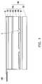
- FIG. 1is a schematic cross-sectional view illustrating a switchable 3D display according to an embodiment of the invention.
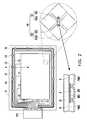
- FIG. 2is a schematic top view illustrating a switchable parallax barrier.
- FIG. 3is a schematic cross-sectional view taken along a cross-section A-A′ depicted in FIG. 2 .
- FIG. 1is a schematic cross-sectional view illustrating a switchable 3D display according to an embodiment of the invention.
- the switchable 3D display 100 of this embodimentincludes a switchable parallax barrier 110 and a display panel 120 .
- the switchable parallax barrier 110is configured over the display panel 120 .
- the switchable parallax barrier 110includes a first substrate S 1 , a second substrate S 2 , an insulating layer 112 , a common electrode 114 , and a light-valve layer 116 .
- the first substrate S 1has a touch-sensing circuit 118 .
- the second substrate S 2has a plurality of control electrodes 119 and is configured between the first substrate S 1 and the display panel 120 .
- the touch-sensing circuit 118 and the control electrodes 119are located between the first substrate S 1 and the second substrate S 2 .
- the insulating layer 112is configured over the first substrate S 1 to cover the touch-sensing circuit 118 .
- the common electrode 114is configured on the insulating layer 112 .
- the light-valve layer 116is configured between the common electrode 114 and the control electrodes 119 . Namely, the common electrode 114 is located between the insulating layer 112 and the light-valve layer 116 .
- the display panel 120 of this embodimentcan be any type of flat display panel, such as a liquid crystal display (LCD) panel, an organic electro-luminescent display panel, a plasma display panel, an electrophoretic display panel, and so on.
- LCDliquid crystal display
- organic electro-luminescent display panelorganic electro-luminescent display panel
- plasma display panelorganic electro-luminescent display panel
- electrophoretic display paneland so on.
- the LCD panelcan achieve favorable display performance when an appropriate backlight unit is applied.
- the insulating layer 112is located between the common electrode 114 and the touch-sensing circuit 118 , so as to ensure that abnormal short circuit does not exist between the common electrode 114 and the touch-sensing circuit 118 .
- the light-valve layer 116 located between the common electrode 114 and the control electrodes 119can have different transmittances in partial regions of the light-valve layer 116 .
- the light-valve layer 116is a liquid crystal layer
- the control electrodes 119are a plurality of bar-shaped electrodes parallel to one another, for instance.
- the control electrodes 119define a plurality of slits S parallel to one another, and the width of the slits S and the pitch between the slits S can be appropriately modified based on the distance between pixels on the display panel 120 .
- the transmittance of the light-valve layer 116 above the control electrodes 119can be significantly reduced because of the voltage difference between the common electrode 114 and the control electrodes 119 (the transmittance approaches zero).
- the images displayed on the display panel 120can be merely seen by a viewer through the slits S, and the images seen by the viewer are the 3D images.
- the light-valve layer 116can be made of a normally white liquid crystal, for instance.
- the switchable parallax barrier 110When the switchable parallax barrier 110 is not switched on, i.e., there is no voltage difference between the common electrode 114 and the control electrodes 119 , the images displayed on the display panel 120 can successfully pass through the light-valve layer 116 , so as to achieve the 2D display effect.
- the light-valve layer 116 made of the normally white liquid crystalgives rise to power consumption.
- the light-valve layer 116is not limited to be made of the normally white liquid crystal in this invention.
- the material of the light-valve layer 116can be determined based on the design requirements for products.
- the touch-sensing circuit 118 , the insulating layer 112 , and the common electrode 114are formed on an inner surface of the first substrate S 1
- the control electrodes 119are formed on an inner surface of the second substrate S 2
- the space between the first substrate S 1 and the second substrate S 2is filled with the light-valve layer 116 (e.g., the liquid crystal layer) after the first substrate S 1 and the second substrate S 2 are assembled.
- the fabrication of the switchable parallax barrier 110 having the touch-sensing circuit 118requires two substrates (i.e., the first and the second substrates S 1 and S 2 ). Therefore, the entire thickness and the manufacturing costs of the switchable parallax barrier 110 can be further reduced.
- FIG. 2is a schematic top view illustrating a switchable parallax barrier.
- FIG. 3is a schematic cross-sectional view taken along a cross-section A-A′ depicted in FIG. 2 .
- the touch-sensing circuit 118 of this embodimentis a capacitive touch-sensing circuit, for instance.
- the touch-sensing circuit 118is constituted by a plurality of first sensing series SS 1 electrically insulated from one another and a plurality of second sensing series SS 2 electrically insulated from one another.
- First sensing pads PAD 1 and first bridge lines BR 1 in the first sensing series SS 1 and second sensing pads PAD 2 in the second sensing series SS 2can be formed by a patterned transparent conductive layer, for instance.
- Second bridge lines BR 2 connected to the adjacent second sensing pads PAD 2 in the second sensing series SS 2are metal bridge lines with satisfactory electrical conductivity, for instance.
- the second bridge lines BR 2 and the first bridge lines BR 1are electrically insulated at the intersections of the first and the second bridge lines BR 1 and BR 2 because a dielectric material D is disposed therebetween.
- the second bridge lines BR 2can be formed before or after the patterned transparent conductive layer is formed, which is not limited in the invention.
- the first sensing seriescan be formed by a patterned transparent conductive layer
- the second sensing seriescan be formed by another patterned transparent conductive layer.
- the first and the second sensing seriesare electrically insulated at the intersections of the two sensing series because the dielectric material is disposed therebetween.
- the type of the touch-sensing circuit 118 and a method of forming the sameare not limited in the invention.
- the touch-sensing circuit 118 on the first substrate S 1not only includes the first and the second sensing series SS 1 and SS 2 but also includes a plurality of touch-sensing signal transmission circuits C 1 .
- Each of the touch-sensing signal transmission circuits C 1is connected to the corresponding first sensing series SS 1 or the corresponding second sensing series SS 2 , so as to transmit touch-sensing signals to the control circuit board or other control units.
- the first substrate S 1can further include at least one control signal transmission wiring C 2
- the switchable parallax barrier 110can further include at least one conductive element C 3 .
- the conductive element C 3is configured between the first substrate S 1 and the second substrate S 2 , and the control electrodes 119 are electrically connected to the control signal transmission wiring C 2 through the conductive element C 3 .
- the conductive element C 3can be an Au ball, a ball-shaped element made of other materials, or a conductive post made of any material as long as the Au ball, the ball-shaped element, or the conductive post has favorable electrical conductivity.
- the conductive element C 3is electrically connected to the control signal transmission wiring C 2 through a transfer pad T.
- the transfer pad T and the common electrode 114are made of the same material, such as indium tin oxide, indium zinc oxide, or other transparent conductive materials.
- the transfer pad Tis farmed at the same time with the common electrode 114 , for instance.
- a sealant SLcan be configured between the first substrate S 1 and the second substrate S 2 .
- the sealant SLnot only can encapsulate the conductive element C 3 but also can surround the light-valve layer 116 , such that the light-valve layer 116 is sealed between the first substrate S 1 and the second substrate S 2 .
- the common electrode 114can be connected to a conductive circuit C 4 formed on the second substrate S 2 through at least one contact window.
- the touch-sensing signal transmission circuits C 1 , the control signal transmission wiring C 2 , and the conductive circuit C 4can be formed at the same time with a conductive thin film in the touch-sensing circuit 118 .
- the touch-sensing signal transmission circuits C 1 , the control signal transmission wiring C 2 , and the conductive circuit C 4are formed at the same time with the second bridge lines BR 2 , for instance.
- the touch-sensing signal transmission circuits C 1 , the control signal transmission wiring C 2 , and the conductive circuit C 4 in this embodimentare converged at the edge of the first substrate S 1 and electrically connected to the flat printed circuit FPC.
- the switchable parallax barrier 110 of this embodimentcan be electrically connected to the control circuit board or other control units through one flat printed circuit FPC. Hence, the assembly of the switchable parallax barrier 110 is rather simple and fast.
- the touch-sensing circuitis integrated into the switchable parallax barrier in this invention, which contributes to mass production of the switchable 3D display and reduction of the entire thickness and weight of the switchable 3D display of the invention.
Landscapes
- Engineering & Computer Science (AREA)
- General Engineering & Computer Science (AREA)
- Theoretical Computer Science (AREA)
- Human Computer Interaction (AREA)
- Physics & Mathematics (AREA)
- General Physics & Mathematics (AREA)
- Multimedia (AREA)
- Signal Processing (AREA)
- Liquid Crystal (AREA)
- Position Input By Displaying (AREA)
Abstract
Description
Claims (10)
Applications Claiming Priority (3)
| Application Number | Priority Date | Filing Date | Title |
|---|---|---|---|
| TW99137003 | 2010-10-28 | ||
| TW99137003A | 2010-10-28 | ||
| TW099137003ATWI422865B (en) | 2010-10-28 | 2010-10-28 | Switchable three-dimensional display |
Publications (2)
| Publication Number | Publication Date |
|---|---|
| US20120105434A1 US20120105434A1 (en) | 2012-05-03 |
| US8384685B2true US8384685B2 (en) | 2013-02-26 |
Family
ID=45996179
Family Applications (1)
| Application Number | Title | Priority Date | Filing Date |
|---|---|---|---|
| US12/983,330Active2031-06-05US8384685B2 (en) | 2010-10-28 | 2011-01-03 | Switchable three-dimensional display |
Country Status (2)
| Country | Link |
|---|---|
| US (1) | US8384685B2 (en) |
| TW (1) | TWI422865B (en) |
Cited By (4)
| Publication number | Priority date | Publication date | Assignee | Title |
|---|---|---|---|---|
| US20130300705A1 (en)* | 2012-05-09 | 2013-11-14 | Samsung Display Co., Ltd. | Display device for touch sensing and 3-dimensional image display, and driving method thereof |
| US20130329907A1 (en)* | 2012-06-06 | 2013-12-12 | Mingsian R. Bai | Miniture electronic shotgun microphone |
| WO2014153916A1 (en)* | 2013-03-29 | 2014-10-02 | 北京京东方光电科技有限公司 | Liquid crystal grating, 3d touch display device, and method for driving liquid crystal grating |
| US9996200B2 (en)* | 2013-04-27 | 2018-06-12 | Beijing Boe Optoelectronics Technology Co., Ltd. | Touch screen, display device and manufacturing method thereof usable for realizing 3D display |
Families Citing this family (11)
| Publication number | Priority date | Publication date | Assignee | Title |
|---|---|---|---|---|
| TWI474299B (en)* | 2010-08-05 | 2015-02-21 | Display device and method for manufacturing parallax barrier touch plate | |
| US9791950B2 (en)* | 2011-08-31 | 2017-10-17 | Sony Corporation | Liquid crystal display |
| TWI459261B (en)* | 2012-04-16 | 2014-11-01 | Chunghwa Picture Tubes Ltd | Touch sensing three-dimensional display device |
| CN102707514B (en)* | 2012-05-03 | 2014-03-26 | 北京京东方光电科技有限公司 | 3D (3-dimensional) touch liquid crystal lens grating, display device and manufacturing methods of 3D touch liquid crystal lens grating and display device |
| KR101981529B1 (en)* | 2012-05-25 | 2019-05-24 | 엘지디스플레이 주식회사 | Touch sensing apparatus and driving method thereofp |
| TWI486668B (en)* | 2012-05-24 | 2015-06-01 | Chunghwa Picture Tubes Ltd | Panel structure |
| KR101469485B1 (en) | 2012-08-13 | 2014-12-05 | 엘지디스플레이 주식회사 | Organic Emitting Display Device and Method for Manufacturing the Same |
| CN102830555B (en)* | 2012-08-31 | 2015-01-07 | 北京京东方光电科技有限公司 | Touch liquid crystal grating and 3D touch display device |
| US9058780B2 (en)* | 2013-03-08 | 2015-06-16 | Innolux Corporation | 2D/3D switchable and touch sensitive display and method for driving the same |
| CN104391392A (en) | 2014-09-28 | 2015-03-04 | 京东方科技集团股份有限公司 | 3D (three-dimensional) touch display device as well as production method and drive method thereof |
| CN107491203B (en) | 2016-06-13 | 2020-08-11 | 元太科技工业股份有限公司 | touch display device |
Citations (11)
| Publication number | Priority date | Publication date | Assignee | Title |
|---|---|---|---|---|
| US5136409A (en) | 1987-09-29 | 1992-08-04 | Canon Kabushiki Kaisha | Liquid crystal device having at least two zones having different diffusion characteristics |
| US6473141B2 (en) | 1996-07-12 | 2002-10-29 | Sharp Kabushiki Kaisha | Directional display and method of making a mask for a directional display |
| US20040041747A1 (en) | 2002-08-27 | 2004-03-04 | Nec Corporation | 3D image/2D image switching display apparatus and portable terminal device |
| US20060082702A1 (en)* | 2002-06-28 | 2006-04-20 | Jacobs Adrian M S | Optical device and display operating in two dimensional and autostereoscopic three dimensional modes |
| US7245430B2 (en) | 2003-04-21 | 2007-07-17 | Ricoh Company, Ltd. | Method and apparatus for displaying three-dimensional stereo image using light deflector |
| US20070296911A1 (en) | 2006-06-27 | 2007-12-27 | Hyung-Ki Hong | Liquid crystal lens and image display device including the same |
| US7554120B2 (en)* | 2006-08-24 | 2009-06-30 | Seiko Epson Corporation | Circuit board for electro-optical device, electro-optical device, and electronic apparatus |
| US20090185088A1 (en) | 2008-01-21 | 2009-07-23 | Seiko Epson Corporation | Electro-optical device, method of manufacturing electro-optical device, and electronic apparatus |
| US7567307B2 (en)* | 2007-01-05 | 2009-07-28 | Samsung Electronics Co., Ltd. | Highly efficient 2D/3D switchable display device |
| CN101576667A (en) | 2008-05-09 | 2009-11-11 | 奇信电子股份有限公司 | Touch signal transmission circuit and display using same |
| CN101630493A (en) | 2009-07-10 | 2010-01-20 | 天马微电子股份有限公司 | Liquid crystal display device |
Family Cites Families (2)
| Publication number | Priority date | Publication date | Assignee | Title |
|---|---|---|---|---|
| GB2390171A (en)* | 2002-06-28 | 2003-12-31 | Sharp Kk | Optical device and display |
| TWI254830B (en)* | 2005-05-11 | 2006-05-11 | Toppoly Optoelectronics Corp | A liquid crystal display device |
- 2010
- 2010-10-28TWTW099137003Apatent/TWI422865B/enactive
- 2011
- 2011-01-03USUS12/983,330patent/US8384685B2/enactiveActive
Patent Citations (11)
| Publication number | Priority date | Publication date | Assignee | Title |
|---|---|---|---|---|
| US5136409A (en) | 1987-09-29 | 1992-08-04 | Canon Kabushiki Kaisha | Liquid crystal device having at least two zones having different diffusion characteristics |
| US6473141B2 (en) | 1996-07-12 | 2002-10-29 | Sharp Kabushiki Kaisha | Directional display and method of making a mask for a directional display |
| US20060082702A1 (en)* | 2002-06-28 | 2006-04-20 | Jacobs Adrian M S | Optical device and display operating in two dimensional and autostereoscopic three dimensional modes |
| US20040041747A1 (en) | 2002-08-27 | 2004-03-04 | Nec Corporation | 3D image/2D image switching display apparatus and portable terminal device |
| US7245430B2 (en) | 2003-04-21 | 2007-07-17 | Ricoh Company, Ltd. | Method and apparatus for displaying three-dimensional stereo image using light deflector |
| US20070296911A1 (en) | 2006-06-27 | 2007-12-27 | Hyung-Ki Hong | Liquid crystal lens and image display device including the same |
| US7554120B2 (en)* | 2006-08-24 | 2009-06-30 | Seiko Epson Corporation | Circuit board for electro-optical device, electro-optical device, and electronic apparatus |
| US7567307B2 (en)* | 2007-01-05 | 2009-07-28 | Samsung Electronics Co., Ltd. | Highly efficient 2D/3D switchable display device |
| US20090185088A1 (en) | 2008-01-21 | 2009-07-23 | Seiko Epson Corporation | Electro-optical device, method of manufacturing electro-optical device, and electronic apparatus |
| CN101576667A (en) | 2008-05-09 | 2009-11-11 | 奇信电子股份有限公司 | Touch signal transmission circuit and display using same |
| CN101630493A (en) | 2009-07-10 | 2010-01-20 | 天马微电子股份有限公司 | Liquid crystal display device |
Non-Patent Citations (1)
| Title |
|---|
| "First Office Action of China Counterpart Application", issued on Nov. 23, 2011, p. 1-p. 5. |
Cited By (6)
| Publication number | Priority date | Publication date | Assignee | Title |
|---|---|---|---|---|
| US20130300705A1 (en)* | 2012-05-09 | 2013-11-14 | Samsung Display Co., Ltd. | Display device for touch sensing and 3-dimensional image display, and driving method thereof |
| US8976137B2 (en)* | 2012-05-09 | 2015-03-10 | Samsung Display Co., Ltd. | Display device for touch sensing and 3-dimensional image display, and driving method thereof |
| US20130329907A1 (en)* | 2012-06-06 | 2013-12-12 | Mingsian R. Bai | Miniture electronic shotgun microphone |
| US9148723B2 (en)* | 2012-06-06 | 2015-09-29 | National Tsing Hua University | Miniature electronic shotgun microphone |
| WO2014153916A1 (en)* | 2013-03-29 | 2014-10-02 | 北京京东方光电科技有限公司 | Liquid crystal grating, 3d touch display device, and method for driving liquid crystal grating |
| US9996200B2 (en)* | 2013-04-27 | 2018-06-12 | Beijing Boe Optoelectronics Technology Co., Ltd. | Touch screen, display device and manufacturing method thereof usable for realizing 3D display |
Also Published As
| Publication number | Publication date |
|---|---|
| US20120105434A1 (en) | 2012-05-03 |
| TW201217835A (en) | 2012-05-01 |
| TWI422865B (en) | 2014-01-11 |
Similar Documents
| Publication | Publication Date | Title |
|---|---|---|
| US8384685B2 (en) | Switchable three-dimensional display | |
| KR101611906B1 (en) | Stereoscopic Liquid Crystal Display Device Having Touch Panel and Method for Manufacturing the Same | |
| US10009599B2 (en) | Touch glasses-free grating 3D display device and manufacturing and control methods thereof | |
| US8687135B2 (en) | Stereoscopic liquid crystal display device having touch panel and method for manufacturing the same | |
| US8884922B2 (en) | Display device including touch panel and parallax barrier sharing single board | |
| US9280014B2 (en) | Liquid crystal display device with touch function | |
| CN102073161B (en) | Switchable Stereoscopic Display | |
| US10082903B2 (en) | Display panel and display device | |
| CN103293786B (en) | Display device and liquid crystal barrier device | |
| US20130155059A1 (en) | Switchable touch stereoscopic image device | |
| US11009732B2 (en) | Display panel and display device | |
| US9857616B2 (en) | Touch sensing optical system and display device including the same | |
| US20190332219A1 (en) | Touch-control display panel, driving method and touch-control display device | |
| EP3009884B1 (en) | Flat panel display with narrow bezel area | |
| KR20130068096A (en) | Liquid crystal display device having touch and three dimensional display functions and method for manufacturing the same | |
| US20120050190A1 (en) | Display apparatus | |
| CN109839779A (en) | Liquid crystal display panel | |
| CN102323702B (en) | Liquid crystal lens | |
| US20180335657A1 (en) | Display panel and display device | |
| CN102736309B (en) | Display floater, display unit and electronic equipment | |
| US9454228B2 (en) | Vibrating touch panel display | |
| KR20160053839A (en) | 3D Panel, Manufacturing Method Thereof and 3D Display Device Therewith | |
| CN107608565B (en) | Touch display panel and touch display device | |
| CN109656063B (en) | Array substrate, display panel and display device | |
| US10732447B2 (en) | Touch panel and electronic device |
Legal Events
| Date | Code | Title | Description |
|---|---|---|---|
| AS | Assignment | Owner name:AU OPTRONICS CORPORATION, TAIWAN Free format text:ASSIGNMENT OF ASSIGNORS INTEREST;ASSIGNORS:KUO, YA-LING;YEH, CHIA-CHUN;REEL/FRAME:025604/0156 Effective date:20101221 | |
| STCF | Information on status: patent grant | Free format text:PATENTED CASE | |
| FPAY | Fee payment | Year of fee payment:4 | |
| MAFP | Maintenance fee payment | Free format text:PAYMENT OF MAINTENANCE FEE, 8TH YEAR, LARGE ENTITY (ORIGINAL EVENT CODE: M1552); ENTITY STATUS OF PATENT OWNER: LARGE ENTITY Year of fee payment:8 | |
| AS | Assignment | Owner name:AUO CORPORATION, TAIWAN Free format text:CHANGE OF NAME;ASSIGNOR:AU OPTRONICS CORPORATION;REEL/FRAME:067797/0978 Effective date:20220718 | |
| AS | Assignment | Owner name:SAMSUNG DISPLAY CO., LTD., KOREA, REPUBLIC OF Free format text:ASSIGNMENT OF ASSIGNORS INTEREST;ASSIGNOR:AUO CORPORATION;REEL/FRAME:068323/0055 Effective date:20240627 | |
| MAFP | Maintenance fee payment | Free format text:PAYMENT OF MAINTENANCE FEE, 12TH YEAR, LARGE ENTITY (ORIGINAL EVENT CODE: M1553); ENTITY STATUS OF PATENT OWNER: LARGE ENTITY Year of fee payment:12 |