US8384365B2 - Multi-phase modulator - Google Patents
Multi-phase modulatorDownload PDFInfo
- Publication number
- US8384365B2 US8384365B2US12/136,651US13665108AUS8384365B2US 8384365 B2US8384365 B2US 8384365B2US 13665108 AUS13665108 AUS 13665108AUS 8384365 B2US8384365 B2US 8384365B2
- Authority
- US
- United States
- Prior art keywords
- phases
- power converter
- phase
- digital
- phase modulator
- Prior art date
- Legal status (The legal status is an assumption and is not a legal conclusion. Google has not performed a legal analysis and makes no representation as to the accuracy of the status listed.)
- Expired - Fee Related, expires
Links
Images


Classifications
- H—ELECTRICITY
- H03—ELECTRONIC CIRCUITRY
- H03K—PULSE TECHNIQUE
- H03K7/00—Modulating pulses with a continuously-variable modulating signal
- H03K7/08—Duration or width modulation ; Duty cycle modulation
- H—ELECTRICITY
- H02—GENERATION; CONVERSION OR DISTRIBUTION OF ELECTRIC POWER
- H02M—APPARATUS FOR CONVERSION BETWEEN AC AND AC, BETWEEN AC AND DC, OR BETWEEN DC AND DC, AND FOR USE WITH MAINS OR SIMILAR POWER SUPPLY SYSTEMS; CONVERSION OF DC OR AC INPUT POWER INTO SURGE OUTPUT POWER; CONTROL OR REGULATION THEREOF
- H02M3/00—Conversion of DC power input into DC power output
- H02M3/02—Conversion of DC power input into DC power output without intermediate conversion into AC
- H02M3/04—Conversion of DC power input into DC power output without intermediate conversion into AC by static converters
- H02M3/10—Conversion of DC power input into DC power output without intermediate conversion into AC by static converters using discharge tubes with control electrode or semiconductor devices with control electrode
- H02M3/145—Conversion of DC power input into DC power output without intermediate conversion into AC by static converters using discharge tubes with control electrode or semiconductor devices with control electrode using devices of a triode or transistor type requiring continuous application of a control signal
- H02M3/155—Conversion of DC power input into DC power output without intermediate conversion into AC by static converters using discharge tubes with control electrode or semiconductor devices with control electrode using devices of a triode or transistor type requiring continuous application of a control signal using semiconductor devices only
- H02M3/156—Conversion of DC power input into DC power output without intermediate conversion into AC by static converters using discharge tubes with control electrode or semiconductor devices with control electrode using devices of a triode or transistor type requiring continuous application of a control signal using semiconductor devices only with automatic control of output voltage or current, e.g. switching regulators
- H02M3/158—Conversion of DC power input into DC power output without intermediate conversion into AC by static converters using discharge tubes with control electrode or semiconductor devices with control electrode using devices of a triode or transistor type requiring continuous application of a control signal using semiconductor devices only with automatic control of output voltage or current, e.g. switching regulators including plural semiconductor devices as final control devices for a single load
- H02M3/1584—Conversion of DC power input into DC power output without intermediate conversion into AC by static converters using discharge tubes with control electrode or semiconductor devices with control electrode using devices of a triode or transistor type requiring continuous application of a control signal using semiconductor devices only with automatic control of output voltage or current, e.g. switching regulators including plural semiconductor devices as final control devices for a single load with a plurality of power processing stages connected in parallel
Definitions
- the instant inventionrelates to a multi-phase modulator for a multi-phase power converter.
- a high performance multi-phase modulatoris a component in multi-phase power supplies.
- PWMpulse-width modulators
- An N-phase systemrequires N high-resolution digital pulse-width modulators, which limits the scalability of these approaches.
- This approachis based on the assumption that all phases operate with exactly the same duty cycle over each switching period T s , and that the pattern of switching transitions for individual phases can be determined based on the duty-cycle command once per switching period T s .
- This architectureleads to an efficient, scalable hardware realization, but limits the update rate to the switching frequency f s .
- a multi-phase modulator for a multi-phase power converteris provided.
- a multi-phase modulator for a multi-phase power convertercomprises a a multi-phase power converter, a decoder, and a selector.
- the multi-phase power convertercomprises a plurality of power converter phases.
- the decoderreceives a digital input command and determines a first number of phases of the plurality of power converter phases to place in a first state based upon the digital input command.
- the selectoridentifies a first set of phases of the plurality of power converter phases to assign to the first state and a second set of phases of the plurality of power converter phases to assign to a second state.
- thermometer-code digital commandrepresents a first state and a second state for each of a plurality of bits corresponding to a plurality of phases of a multi-phase power converter to be controlled.
- the methodcomprises: receiving a digital input command; determining, from the digital input command, a first number of output bits of the modulated thermometer-code digital command to place in the first state; determining a first set of bits to be assigned a first value representing the first state and a second set of bits to be assigned a second value representing the second state; and providing the multi-phase modulated thermometer-code digital command to a multi-phase power converter comprising a plurality of power converter phases in which the first set of bits are assigned the first value representing the first state and the second set of bits are assigned the second value.
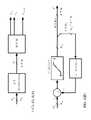
- FIG. 1shows one implementation of a multi-phase DC-DC converter with N phases operating in parallel.
- FIG. 2shows an equivalent N-level power D/A view of the control loop of FIG. 1 using a Thevenin equivalent N-level power digital-to-analog (D/A) converter.
- D/Adigital-to-analog
- FIG. 3shows a general block diagram of one implementation of an MPM architecture.
- FIG. 4(A)shows an example of a resolution improvement using a sigma-delta ( ⁇ ) modulator in front of a multi-phase modulator.
- FIG. 4Bshows an example implementation of a ⁇ modulator following an error-feedback ⁇ architecture.
- FIG. 5shows one implementation of an MPM realization according to the architecture shown in FIG. 2 .
- FIG. 6shows an example timing diagram illustrating how MSB and LSB outputs are combined to generate phasing and duty cycle for a given input command.
- FIG. 7shows experimental results for a digital MPM.
- FIG. 8shows experimental results for a digital MPM.
- FIG. 9shows an implementation of a controller architecture for a multi-phase DC-DC converter with N phases operating in parallel.
- FIG. 10shows an example of a block diagram of the system of FIG. 9 including a power D/A N-level view of the N-phase converter.
- FIG. 11shows magnitude and phase responses of a system loop gain for an example multi-phase DC-DC converter.
- FIG. 12shows example step-reference transient simulation results for (a) a 16-level power D/A model, and (b) a complete 16-phase switching converter.
- FIG. 13shows a system 25 MHz MSB clock, a sampling rate, and switch-node voltages v s for two consecutive phases.
- FIG. 14shows experimental step-load transient waveforms captured from an FPGA controller using an on-chip logic analyzer.
- FIG. 15shows another example experimental step reference response.
- FIG. 1shows one implementation of a multi-phase DC-DC converter with N phases operating in parallel to achieve improved power scaling, ripple and dynamic performance.
- each of the N phasescomprises a synchronous buck converter power stage.
- Other converter configurations that may be used in the power stageinclude buck converters, three-level or multi-level converters, step-up, step-down or up-down (buck-boost) converters, converters with coupled inductors, converters with isolation transformers, and monolithic power stages.
- buck-booststep-up, step-down or up-down converters
- converters with coupled inductorsconverters with isolation transformers
- monolithic power stagesmonolithic power stages.
- buck-boostdigital multi-phase modulator
- the MPM architecture and the realizationis based on a multi-phase converter viewed as a multi-level digital-to-analog converter, or power D/A.
- a multi-phase converterviewed as a multi-level digital-to-analog converter, or power D/A.
- D/Apower digital-to-analog converter
- a control system of the multi-phase DC-DC convertercomprises an analog-to-digital (A/D) converter, a digital compensator and the multi-phase modulator.
- An output voltage of the N phase DC-DC converteris sampled and compared to a reference voltage V ref to generate an analog error signal.
- the reference voltage V refcan be dynamically programmed through a digital input.
- a window A/D convertercan be centered around an analog reference voltage V ref , where V ref can be digitally programmed through a digital-to-analog (D/A) converter.
- D/Adigital-to-analog
- an A/D converter with a conversion rangecan be set by an analog reference voltage.
- the system referenceis a direct digital input.
- the error signalis converted to a digital error signal by the A/D converter, which is provided to the digital compensator.
- the A/D convertermay comprise a uniform, non-uniform or programmable quantization characteristic.
- the digital error signal(i.e., the digital equivalent of the difference between the sensed output voltage and the reference can be processed in a number of ways, including a combination of one or more of the following functional blocks: (a) linear discrete-time compensator, such as a PI or PID compensator; (b) nonlinear discrete-time compensator; (c) notch, comb, or other ripple cancellation filter; (d) linear or nonlinear processing of signals obtained by sensing or estimation of power-stage signal such as capacitor currents, inductor currents, inductor voltages, capacitor voltages, switch voltages, switch currents, or combinations of such power stage signals; (e) linear or nonlinear processing of power stage signals to achieve minimum-time responses to changes in load or reference; (f) processing blocks such as dither or s
- the compensator in FIG. 1is a digital compensator
- an alternative compensator designcan be realized as an analog component, followed by an A/D converter to generate the command to the multi-phase modulator.
- the MPM architecture shown in FIG. 1includes a single high-resolution module.
- the MPM input command dcan be updated at any time, which opens the possibilities for wide-bandwidth closed-loop operation.
- FIG. 1shows the control loop sensing an output voltage
- current-sensingcan be added to accomplish one or a combination of the following: (a) improved current sharing, (b) adaptive voltage positioning (using any number of known approaches); (c) improved dynamic responses; and (d) protection.
- the purpose of a digital multi-phase modulatoris to generate the on/off control signals ⁇ c 0 , c 1 , . . . , c N-1 ⁇ for each of the N gate drives in the multi-phase converter system based on the high-resolution (p-bit) input command d.
- p-bithigh-resolution
- the MPMdecides which phases are to be in a given state at a particular time. There are numerous ways to perform such a decision, including one or a combination of the following: (a) order of the phases and phase rotation; (b) activation of the phases to minimize mismatches in per-phase currents; and (c) activation of the phases to minimize the number of switching transitions, i.e., to minimize the system switching losses.
- the MPMmay additionally implement one or a combination of the following additional functions: (a) phase re-ordering, static or dynamic, for example to reduce the effects of phase mismatches; and (b) adjusting the number of operating phases, statically or dynamically, for example to minimize losses at light loads.
- FIG. 3A general block diagram of the proposed MPM architecture is shown in FIG. 3 .
- the MSB command d MSBis the input to the MPM core consisting of a Decoder and a Selector. Based on the input d MSB , the Decoder sets the signals t i to decide how many phases are on. For example, to turn k phases on, we have:
- the Selector shown in FIG. 3decides which k phases are on by mapping the signals t i to the phase on/off control signals c i .
- a single LSB modulecomplements the MPM core to achieve high resolution control based on the m-bit LSB input D LSB .
- the architecture in FIG. 3is very general. The fact that it resembles a standard D/A converter architecture leads immediately to a number of implementation options. For example, if all N phases are nominally identical (as in FIG. 1 ), the Decoder converts the binary input d MSB to a thermometer-code output ⁇ t i ⁇ . If, instead, the phases are logarithmic, no decoding is necessary.
- the Selectorhas to perform a time-dependent mapping from ⁇ t i ⁇ to ⁇ c i ⁇ to accomplish, for example, benefits of ripple minimization and equal current sharing.
- DPWMdigital pulse-width modulation
- FIG. 4(A)illustrates a resolution improvement using a ⁇ modulator in front of an MPM.
- a high resolution n h -bit command signal d his the input o the ⁇ modulator.
- the output of the ⁇ modulatoris the lower-resolution (n+m)-bit command signal d, which is the input to the MPM.
- An implementation of the ⁇ modulatoris shown in FIG. 4(B) , following the error-feedback ⁇ architecture with the noise transfer function NTF(z) designed to suppress the quantization noise at low frequencies using standard ⁇ techniques.
- the multi-phase converter with the MPMbehaves as a power D/A converter with enhanced resolution
- a single n-bit down countere.g. counts in reverse ⁇ 2, 1, 0, 3, . . . ⁇
- N multiplexerscan be used to achieve phase rotation.
- the LSB command d LSBis input to a single DPWM to generate the pulse-width modulated signal t 0 .
- Hardware efficiencyis achieved by time sharing the single high resolution DPWM output t 0 among all N phases.
- Other clock rates both higher and lower than Nf smay be used, however.
- Similar solutionshave been used in audio signal processing D/A converters to achieve high resolution and improved linearity by using phase shifting to allot equal time to each element in the D/A.
- the MSB input command d MSBpasses through the Decoder and the Selector directly to generate the on/off control signals c i .
- the number of on phasesswitches from 3 to 1 instantaneously.
- the fast update rate and the ability to change the number of phases that are on at any timeopens the possibilities for wide-bandwidth closed-loop operation as described in Y. Zhang, X. Zhang, R. Zane, D. Maksimovic, “Wide-bandwidth digital multi-phase controller,” IEEE PESC 2006 and X. Zhang, Y. Zhang, R.
- the ICwas fabricated in a 0.35 ⁇ CMOS process and includes two complete versions of the digital MPM. Both versions include identical copies of the MPM core but with different types of DPWM LSB modules: counter and delay-line based. The area requirements for each of the modules and total MPM designs are shown in Table I.
- DLLdigital delay-locked loop
- FIGS. 7 and 8Experimental results for the digital MPM are shown in FIGS. 7 and 8 . All results were captured using an Agilent 1681AD logic analyzer to capture all sixteen phase outputs and a Tektronix TDS7104 oscilloscope, triggered from the logic analyzer to correlate the waveforms.
- a multi-phase modulatormay utilize a wide-bandwidth digital control method that enables a closed-loop bandwidth that scales with Nf s .
- This approachis closely tied to the equivalent view of the N-phase converter as an N-level power D/A converter as shown in FIG. 2 .
- the equivalent voltage source levelV g /N, 2 V g /N, . . .
- kV g /Nup to V g
- d c⁇ c k ⁇
- N2 n
- the control command of how many phases are activecan, in principle, be given at any time.
- the modulatortakes the task of deciding which phases are active.
- the command d cis constant, and the steady-state operation is exactly the same as in the conventional multi-phase realization with per-phase switching frequency equal to f s .
- the discrete-time compensatorcan be designed using digital control techniques to achieve the system closed-loop bandwidth proportional to Nf s rather than the per-phase switching frequency f s .
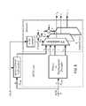
- FIG. 9One implementation of a controller architecture is shown in FIG. 9 .
- the systemcomprises a voltage A/D converter, a digital compensator and a multi-phase modulator.
- FIG. 10shows a block diagram of the system including the power D/A N-level view of the N-phase converter.
- the output voltage v outis sensed and compared to the reference V ref .
- An error signal v eis sampled and converted to the digital error signal e at the rate of Nf s .
- N2 n
- the n most significant bits(MSB) of the command d crepresent how many phases should be active in the next sampling interval (T s /N).
- the multi-phase modulatorcan execute this MSB command immediately, with delays due only to the gate-driver propagation delays.
- all the phasescan be turned active or inactive at the same time as directed by the compensator.
- This featuremay be built into the controller architecture and enabled by the MPM realization, and does not require any specific non-linear action.
- the remaining least-significant bits (LSB) of the command d ccan be treated as a PWM command to the modulator, which provides a high resolution to provide for precise output voltage regulation.
- the command d ccan be constant, and the steady-state operation can be the same as a conventional multi-phase PWM realization with a per-phase switching frequency equal to f s .
- the discrete time compensatorcan be easily designed using standard linear (e.g., PI or PID) digital control techniques to achieve a system closed-loop bandwidth proportional to Nf s .
- a linear digital compensator Gc(z)can be designed directly in discrete time using any of the available methods. Two design examples are provided below.
- the phase marginis 62° and the gain margin is 8.5 dB.
- FIG. 12shows example step reference (1V to 1.05V) transient simulation results for (a) a 16-level power D/A model, and (b) a complete 16-phase switching converter.
- FIG. 13shows a system 25 MHz MSB clock, which in this implementation is equal to the sampling rate, and switch-node voltages v s for two consecutive phases.
- the slopes in the v s voltagesare due to the relatively large per-phase current ripples and relatively large on-resistances of the driver power MOSFETs.
- the phase delay between two consecutive phasesis equal to the MSB clock period of 40 ns. It can be observed that there are driver propagation delay mismatches, which also contribute to the non-ideal ripple cancellations, as discussed above.
- FIGS. 14(A) through 14(C)show experimental step-load transient waveforms captured from an FPGA controller using an on-chip logic analyzer.
- FIG. 14(B)shows the digital command d c .
- FIG. 14(C)shows how the MSB command, i.e., the number of phases that are on, drops abruptly from 5 to 0 at the beginning of the reference step-down transient.
- FIG. 15shows a larger (0.9V to 1. V) experimental step reference response.
- a digital multi-phase modulatorthat leads to an efficient, high performance hardware realization is provided.
- the modulator and converter systemis viewed as a multi-level power D/A to achieve improved performance and hardware efficiency.
- the modulatorcan be split into three functional blocks including a decoder that determines how many phases are on at any time, a selector that determines which phases are on at any time and a single LSB module that is time shared among all phases to achieve high resolution in steady-state.
- the resulting architecturescales favorably with a large number of phases, facilitates fast update rates of the input command well above the single phase switching frequency and is compatible with a wide range of known DPWM techniques for the LSB module and resolution-enhancement techniques such as dithering or ⁇ - ⁇ modulation.
- a method of wide-bandwidth digital controlfor interleaved multi-phase digital converters.
- the methodis based on a view of a multi-phase converter as a multi-level power D/A converter where the output voltage is sampled and the command is updated at a rate of Nf s , where f s is the per-phase switching frequency and N is the number of phases.
- Nf sthe per-phase switching frequency
- This viewenables a very efficient multi-phase modulator design.
- the bandwidthis limited to a fraction of the switching frequency f s a bandwidth that scales with Nf s is achievable.
- System model and linear digital compensator designsare provided.
- a zero-error bin approachwhich is inherent to the digital controller implementation, is proposed to address the effects of phase-mismatches, and sub-harmonic ripples on the stability of the wide-bandwidth controller. Simulation and experimental results are also shown for a 16-phase synchronous buck converter operating at 1.56 MHz per-phase switching frequency.
- joinder referencesdo not necessarily infer that two elements are directly connected and in fixed relation to each other. It is intended that all matter contained in the above description or shown in the accompanying drawings shall be interpreted as illustrative only and not limiting. Changes in detail or structure may be made without departing from the spirit of the invention as defined in the appended claims.
Landscapes
- Engineering & Computer Science (AREA)
- Power Engineering (AREA)
- Dc-Dc Converters (AREA)
Abstract
Description
resembles the characteristic of a standard N-level thermometer code D/A converter. It is important to note that formula (2) implies that the same output voltage level is generated regardless of which k phases are on. This is decided by the Selector, which performs a time-dependent mapping from {ti} to {ci}. In the realization shown in
| TABLE I |
| SUMMARY OF PHYSICAL AREA FOR THE TWO MPM VERSIONS |
| AND MODULES |
| Module | Area | ||
| Counter-based MPM | 0.04 mm2 | ||
| MPM Core | 0.03 mm2 | ||
| Counter LSB | 0.01 mm2 | ||
| Delay-line based MPM | 0.23 mm2 | ||
| MPM Core | 0.03 mm2 | ||
| Delay-line LSB | 0.20 mm2 | ||
T(z)=Gvdz(z)Gc(Z) (4)
Magnitude and phase responses of the system loop gain are shown in
Claims (29)
Priority Applications (1)
| Application Number | Priority Date | Filing Date | Title |
|---|---|---|---|
| US12/136,651US8384365B2 (en) | 2007-06-15 | 2008-06-10 | Multi-phase modulator |
Applications Claiming Priority (2)
| Application Number | Priority Date | Filing Date | Title |
|---|---|---|---|
| US94448307P | 2007-06-15 | 2007-06-15 | |
| US12/136,651US8384365B2 (en) | 2007-06-15 | 2008-06-10 | Multi-phase modulator |
Publications (2)
| Publication Number | Publication Date |
|---|---|
| US20080310200A1 US20080310200A1 (en) | 2008-12-18 |
| US8384365B2true US8384365B2 (en) | 2013-02-26 |
Family
ID=62067292
Family Applications (1)
| Application Number | Title | Priority Date | Filing Date |
|---|---|---|---|
| US12/136,651Expired - Fee RelatedUS8384365B2 (en) | 2007-06-15 | 2008-06-10 | Multi-phase modulator |
Country Status (1)
| Country | Link |
|---|---|
| US (1) | US8384365B2 (en) |
Cited By (3)
| Publication number | Priority date | Publication date | Assignee | Title |
|---|---|---|---|---|
| TWI566527B (en)* | 2014-05-30 | 2017-01-11 | 台灣積體電路製造股份有限公司 | Driving circuit, delay controlling circuit and method of operating driving circuit |
| US20200136637A1 (en)* | 2018-10-26 | 2020-04-30 | Maxlinear, Inc. | Method and system for ripple suppression in multi-phase buck converters |
| US10996732B2 (en)* | 2018-03-23 | 2021-05-04 | Chengdu Monolithic Power Systems Co., Ltd. | Slew rate controlled power supply and associated control method |
Families Citing this family (60)
| Publication number | Priority date | Publication date | Assignee | Title |
|---|---|---|---|---|
| US8384365B2 (en)* | 2007-06-15 | 2013-02-26 | The Regents Of The University Of Colorado, A Body Corporate | Multi-phase modulator |
| US8502821B2 (en)* | 2008-02-04 | 2013-08-06 | C Speed, Llc | System for three-dimensional rendering of electrical test and measurement signals |
| US7741983B1 (en) | 2008-12-05 | 2010-06-22 | Google Inc. | Auto-measurement and calibration of DC resistance in current sensing applications |
| KR101679755B1 (en) | 2009-01-23 | 2016-11-28 | 삼성전자주식회사 | Clock signal generator for having fast locking time |
| WO2010151851A1 (en)* | 2009-06-26 | 2010-12-29 | Syntropy Systems | Sampling/quantization converters |
| US9209829B2 (en) | 2009-06-26 | 2015-12-08 | Syntropy Systems, Llc | Sampling/quantization converters |
| US9680498B2 (en) | 2009-06-26 | 2017-06-13 | Syntropy Systems, Llc | Sampling/quantization converters |
| US8917198B2 (en) | 2010-01-05 | 2014-12-23 | Syntropy Systems, Llc | Multi-mode sampling/quantization converters |
| US9419637B1 (en) | 2010-01-05 | 2016-08-16 | Syntropy Systems, Llc | Multi-mode sampling/quantization converters |
| US8299947B2 (en)* | 2009-06-26 | 2012-10-30 | Syntropy Systems, Llc | Sampling/quantization converters |
| US9130584B1 (en) | 2010-01-05 | 2015-09-08 | Syntropy Systems, Llc | Multi-mode sampling/quantization converters |
| US8943112B2 (en) | 2009-06-26 | 2015-01-27 | Syntropy Systems, Llc | Sampling/quantization converters |
| EP2276159A1 (en) | 2009-07-16 | 2011-01-19 | University of Limerick | A digital pulse width modulator |
| US8344706B2 (en)* | 2009-08-10 | 2013-01-01 | Emerson Climate Technologies, Inc. | System and method for rejecting DC current in power factor correction systems |
| US8406021B2 (en)* | 2009-08-10 | 2013-03-26 | Emerson Climate Technologies, Inc. | System and method for reducing line current distortion |
| US8698433B2 (en) | 2009-08-10 | 2014-04-15 | Emerson Climate Technologies, Inc. | Controller and method for minimizing phase advance current |
| US8264192B2 (en) | 2009-08-10 | 2012-09-11 | Emerson Climate Technologies, Inc. | Controller and method for transitioning between control angles |
| US8508166B2 (en)* | 2009-08-10 | 2013-08-13 | Emerson Climate Technologies, Inc. | Power factor correction with variable bus voltage |
| US8264860B2 (en)* | 2009-08-10 | 2012-09-11 | Emerson Climate Technologies, Inc. | System and method for power factor correction frequency tracking and reference generation |
| US8358098B2 (en)* | 2009-08-10 | 2013-01-22 | Emerson Climate Technologies, Inc. | System and method for power factor correction |
| US8476873B2 (en)* | 2009-08-10 | 2013-07-02 | Emerson Climate Technologies, Inc. | System and method for current balancing |
| US8493014B2 (en) | 2009-08-10 | 2013-07-23 | Emerson Climate Technologies, Inc. | Controller and method for estimating, managing, and diagnosing motor parameters |
| WO2011027300A2 (en) | 2009-09-07 | 2011-03-10 | Koninklijke Philips Electronics N.V. | Electrical energy conversion circuit device |
| TWI393334B (en)* | 2009-10-12 | 2013-04-11 | Richtek Technology Corp | Multi-phase buck converter with phase number compensation and phase number compensation method for a multi-phase buck converter |
| US9654128B2 (en) | 2010-01-05 | 2017-05-16 | Syntropy Systems, Llc | Multi-mode sampling/quantization converters |
| EP2522076B1 (en)* | 2010-01-05 | 2020-07-29 | Christopher Pagnanelli | Multi-mode sampling/quantization converters |
| US8471542B2 (en)* | 2010-05-20 | 2013-06-25 | Google Inc. | Adaptive gate drive power control systems and methods |
| US8441242B2 (en)* | 2010-06-04 | 2013-05-14 | Fuji Electric Co., Ltd. | Digitally controlled integrated DC-DC converter with transient suppression |
| US8558524B2 (en)* | 2010-10-19 | 2013-10-15 | International Rectifier Corporation | Master/slave power supply switch driver circuitry |
| CN102457167B (en)* | 2010-10-19 | 2016-03-16 | 雅达电子国际有限公司 | Multi-level parallel power converter |
| US8710963B2 (en) | 2011-03-14 | 2014-04-29 | Infineon Technologies Ag | Receiver and transmitter receiver system |
| US9148709B2 (en)* | 2011-08-03 | 2015-09-29 | Infineon Technologies Ag | Sensor interface with variable control coefficients |
| GB2493529A (en)* | 2011-08-09 | 2013-02-13 | Nujira Ltd | A voltage-selecting tracking power supply with an asynchronous delta-sigma controller |
| US8994526B2 (en) | 2011-08-18 | 2015-03-31 | Infineon Technologies Ag | Sensor interface making use of virtual resistor techniques |
| KR101854395B1 (en)* | 2011-11-25 | 2018-05-08 | 한국전자통신연구원 | Power control driving device and method thereof |
| US9438219B2 (en) | 2011-12-22 | 2016-09-06 | Intel Corporation | Hybrid digital pulse width modulation (PWM) based on phases of a system clock |
| US8849520B2 (en) | 2012-03-26 | 2014-09-30 | Infineon Technologies Ag | Sensor interface transceiver |
| KR101319989B1 (en)* | 2012-04-25 | 2013-10-18 | 한국에너지기술연구원 | Apparatus and method for controlling plural power converting modules, and apparatus and method for analizing electric energy imbalance |
| US9634593B2 (en) | 2012-04-26 | 2017-04-25 | Emerson Climate Technologies, Inc. | System and method for permanent magnet motor control |
| US9240749B2 (en) | 2012-08-10 | 2016-01-19 | Emerson Climate Technologies, Inc. | Motor drive control using pulse-width modulation pulse skipping |
| JP6034132B2 (en)* | 2012-10-24 | 2016-11-30 | 株式会社ソニー・インタラクティブエンタテインメント | DC / DC converter and game machine using the same |
| CN102946254B (en)* | 2012-12-13 | 2015-05-27 | 成都芯源系统有限公司 | Digital controller and digital control method of multiphase switching converter |
| US9906039B2 (en)* | 2013-03-14 | 2018-02-27 | Combind Energies, LLC | Power system for multiple power sources |
| US20140278709A1 (en) | 2013-03-14 | 2014-09-18 | Combined Energies LLC | Intelligent CCHP System |
| US9178433B2 (en)* | 2013-05-15 | 2015-11-03 | Bel Fuse (Macao Commercial Offshore) Limited | Droop current sharing power converter with controlled transitions between regulation set points |
| US9292409B2 (en) | 2013-06-03 | 2016-03-22 | Infineon Technologies Ag | Sensor interfaces |
| US20150002115A1 (en)* | 2013-07-01 | 2015-01-01 | Texas Instruments Incorporated | Series-capacitor buck converter multiphase controller |
| US9344038B2 (en)* | 2014-02-07 | 2016-05-17 | Qualcomm Incorporated | Tri-phase digital polar modulator |
| US9401638B2 (en)* | 2014-03-05 | 2016-07-26 | Texas Instruments Deutschland Gmbh | System and method for single phase transition for multiphase DCDC converters |
| JP5897642B2 (en)* | 2014-05-30 | 2016-03-30 | ファナック株式会社 | DC / DC converter |
| FR3031851B1 (en) | 2015-01-15 | 2017-02-17 | Amcad Eng | CRETE POWER MONITORING SYSTEM FOR RF POWER AMPLIFICATION AND METHOD OF CALCULATING THE CRETE VALUE AND POWER SUPPLY VOLTAGE SELECTION |
| US9621175B2 (en) | 2015-02-11 | 2017-04-11 | Syntropy Systems, Llc | Sampling/quantization converters |
| JP6749231B2 (en)* | 2016-12-27 | 2020-09-02 | 株式会社京三製作所 | POWER SUPPLY DEVICE AND POWER SUPPLY DEVICE CONTROL METHOD |
| CN107707119B (en)* | 2017-09-26 | 2018-09-28 | 中原工学院 | A kind of DC-DC parallel operation systems based on three-phase bridge |
| CN110277894A (en)* | 2019-06-21 | 2019-09-24 | 成都芯源系统有限公司 | Controller of multiphase switching converter and control method thereof |
| EP4008050A4 (en)* | 2019-08-04 | 2022-09-14 | B.G. Negev Technologies and Applications Ltd., at Ben-Gurion University | Digital zero-current switching lock-in controller ic for optimized operation of resonant switched-capacitor converters (sccs) |
| US11936296B2 (en)* | 2019-08-04 | 2024-03-19 | B.G. Negev Technologies And Applications Ltd., At Ben-Gurion University | Digital controller for high-performance multiphase VRM with current balancing and near-ideal transient response |
| CN111898282B (en)* | 2020-08-14 | 2023-02-21 | 天津大学 | Improved modularized multi-level converter Thevenin equivalent modeling method |
| US11996866B2 (en)* | 2022-03-21 | 2024-05-28 | xMEMS Labs, Inc. | Feedback control system achieving high performance via density modulation |
| US20250070643A1 (en)* | 2023-08-23 | 2025-02-27 | Renesas Electronics Corporation | A power stage controller |
Citations (9)
| Publication number | Priority date | Publication date | Assignee | Title |
|---|---|---|---|---|
| US20050110472A1 (en)* | 2003-11-25 | 2005-05-26 | Intersil Americas Inc. | Multiphase DC-DC converter with reduced ripple |
| USRE38846E1 (en)* | 1999-09-01 | 2005-10-25 | Intersil Communications, Inc. | Multi-phase converter with balanced currents |
| US20060055381A1 (en)* | 2004-09-10 | 2006-03-16 | Semiconductor Components Industries, Llc. | Method of forming a multi-phase power supply controller |
| US20060132110A1 (en)* | 2004-12-21 | 2006-06-22 | Primarion, Inc. | Fine resolution pulse width modulation pulse generator for use in a multiphase pulse width modulated voltage regulator |
| US20070035280A1 (en)* | 2005-08-11 | 2007-02-15 | Sharp Kabushiki Kaisha | Power-supply semiconductor integrated circuit, power-supply semiconductor integrated circuit system, development assisting system for power-supply circuit, and program and storage medium therefor |
| US20070096704A1 (en)* | 2005-10-31 | 2007-05-03 | Praveen Jain | Digital controller for a voltage regulator module |
| US20080310200A1 (en)* | 2007-06-15 | 2008-12-18 | The Regents Of The University Of Colorado | Multi-phase modulator |
| US7584371B2 (en)* | 2005-03-17 | 2009-09-01 | International Rectifier Corporation | POL system architecture with analog bus |
| US7773016B2 (en)* | 2008-09-29 | 2010-08-10 | Analog Devices, Inc. | Switching converters controlled via sigma delta modulation |
- 2008
- 2008-06-10USUS12/136,651patent/US8384365B2/ennot_activeExpired - Fee Related
Patent Citations (9)
| Publication number | Priority date | Publication date | Assignee | Title |
|---|---|---|---|---|
| USRE38846E1 (en)* | 1999-09-01 | 2005-10-25 | Intersil Communications, Inc. | Multi-phase converter with balanced currents |
| US20050110472A1 (en)* | 2003-11-25 | 2005-05-26 | Intersil Americas Inc. | Multiphase DC-DC converter with reduced ripple |
| US20060055381A1 (en)* | 2004-09-10 | 2006-03-16 | Semiconductor Components Industries, Llc. | Method of forming a multi-phase power supply controller |
| US20060132110A1 (en)* | 2004-12-21 | 2006-06-22 | Primarion, Inc. | Fine resolution pulse width modulation pulse generator for use in a multiphase pulse width modulated voltage regulator |
| US7584371B2 (en)* | 2005-03-17 | 2009-09-01 | International Rectifier Corporation | POL system architecture with analog bus |
| US20070035280A1 (en)* | 2005-08-11 | 2007-02-15 | Sharp Kabushiki Kaisha | Power-supply semiconductor integrated circuit, power-supply semiconductor integrated circuit system, development assisting system for power-supply circuit, and program and storage medium therefor |
| US20070096704A1 (en)* | 2005-10-31 | 2007-05-03 | Praveen Jain | Digital controller for a voltage regulator module |
| US20080310200A1 (en)* | 2007-06-15 | 2008-12-18 | The Regents Of The University Of Colorado | Multi-phase modulator |
| US7773016B2 (en)* | 2008-09-29 | 2010-08-10 | Analog Devices, Inc. | Switching converters controlled via sigma delta modulation |
Non-Patent Citations (26)
| Title |
|---|
| Carosa, Tony et al., "Digital Multiphase Modulator-A Power D/A Perspecive", Colorado Power Electronics Center, Department of Electrical and Computer Engineering, University of Colorado, Boulder, CO 80309-0425, USA no date given, 6 pages. |
| Carosa, Tony et al., "Implementation of a 16 Phase Digital Modulator in a 0.35 um Process", Colorado Power Electronics Center, Department of Electrical and Computer Engineering, University of Colorado, Boulder, CO 80309-0425, USA no date given, 7 pages. |
| Foley, Raymond F. et al. "An area-efficient digital pulsewidth modulation architecture suitable for FPGA implementation", IEEE APEC 2005, vol. 3, pp. 1412-1418. |
| Garcia, O. et al. "Effect of the Tolerances in Multi-Phase DC-DC Converters", Power Electronics Specialists 2005, IEEE 36th Conference pp. 1452-1457. |
| Huang, Wenkang, "A new control for multi-phase buck converter with fast transient response", IEEE Applied Power Electronics Conference and Exposition 2001, APEC '01, pp. 273-279. |
| Huang, Wenkang, "The design of a high-frequency multiphase voltage regulator with adaptive voltage positioning and all ceramic capacitors", IEEE Applied Power Electronics Conference and Exposition 2005 pp. 270-275. |
| Lee, Kisun et al. "A novel control method for multiphase voltage regulators", IEEE Applied Power Electronics Conference and Exposition 2003, pp. 738-743. |
| Miao, Botao et al. "Automated digital controller design for switching converters", IEEE Power Electronics Specialists, 2005, pp. 2729-2735. |
| O'Malley, Eamon et al "A Programmable Digital Pulse width modulator providing versatile pulse patters and supporting switching frequencies beyond 15 MHz", IEEE APEC, vol. 1, 2004, pp. 53-59. |
| Peterchev, Angel V. et al. "Design of ceramic-capacitor VRM's with estimated load current feed forward", 35th Annual IEEE Power Electronics Specialists Conference, 2004, pp. 4325-4332. |
| Peterchev, Angel V. et al., "Architecture and IC Implementation of a Digital VRM Controller", IEEE Transactions on Power Electronics, vol. 18, No. 1, Jan. 2003, pp. 356-364. |
| Peterchev, Angel V. et al., "Quantization Resolution and Limit Cycling in Digitally Controlled PWM Converters", IEEE Transactions on Power Electronics, vol. 18, No. 1, Jan. 2003, pp. 301-308. |
| Prodic, Aleksandar et al. "Dead-zone digital controller for improved dynamic response of power factor preregulators", IEEE Applied Power Electronics Conference 2003, pp. 382-388. |
| Prodic, Aleksandar et al. "Self-turning digitally controlled low-harmonic rectifier having fast dynamic response", IEEE Transactions on Power Electronics, vol. 18, No. 1, Jan. 2003, pp. 420-428. |
| Qiu, Yang et al. "High-bandwidth designs for voltage regulators with peak-current control", IEEE Applied Power Electronics Conference and Exposition 2006, pp. 24-30. |
| Qiu, Yang et al. "The multi-frequency small-signal model for buck and multiphase interleaving buck converters", IEEE Applied Power Electronics Conference and Exposition 2005, pp. 392-398. |
| Soto, A. et al. "Non-linear digital control breaks bandwidth limitations", IEEE Applied Power Electronics Conference and Exposition 2006, pp. 724-730. |
| Van Tuijl, Ed et al. "A 128 f(subscript s) Multi-Bit Sigma Delta CMOS Audio DAC with Real-Time DEM and 115 dB SFDR", IEEE International Solid-State Circuits Conference, vol. 11, 2004. 8 pages. |
| Van Tuijl, Ed et al. "A 128 f(subscript s) Multi-Bit Σ Δ CMOS Audio DAC with Real-Time DEM and 115 dB SFDR", IEEE International Solid-State Circuits Conference, vol. 11, 2004. 8 pages. |
| Wong, Pit-Leong et al. "Voltage regulator module (VRM) transient modeling and analysis", IEEE Industry Applications Conference 1999, vol. 3, pp. 1669-1676. |
| Wong, Pit-Leong et al., "Critical Inductance in Voltage Regulator Modules", IEEE Transactions on Power Electronics, vol. 17, No. 4, Jul. 2002, pp. 485-592. |
| Wu, Albert M. et al."Digital PWM Control: Application in Voltage Regulation Modules", IEEE Power Electronics Specialists Conference, vol. 1, 1999, pp. 77-83. |
| Yao, Kaiwei et al. "Optimal design of the active droop control method for the transient response", IEEE Applied Power Electronics Conference and Exposition 2003, pp. 718-723. |
| Yousefzadeh, Vahid et al. "Hybrid DPWM with Digital Delay-Locked Loop", IEEE workshop, Rensselaer Polytechnic Institute, Troy, NY, Jul. 16-19, 2006, pp. 142-148. |
| Zhang, X. et al., "A Novel VRM control with direct lead current feedback", IEEE Applied Power Electronics Conference and Exposition 2004, vol. 1, pp. 267-271. |
| Zhang, Yang et al., "Wide-Bandwidth Digital Multi-Phase Controller", Colorado Power Electronics Center, University of Colorado, Boulder, CO 80309-0425, US, no date given, 7 pages. |
Cited By (7)
| Publication number | Priority date | Publication date | Assignee | Title |
|---|---|---|---|---|
| TWI566527B (en)* | 2014-05-30 | 2017-01-11 | 台灣積體電路製造股份有限公司 | Driving circuit, delay controlling circuit and method of operating driving circuit |
| US9735764B2 (en) | 2014-05-30 | 2017-08-15 | Taiwan Semiconductor Manufacturing Company, Ltd. | Circuit and method of operating circuit |
| US10164621B2 (en) | 2014-05-30 | 2018-12-25 | Taiwan Semiconductor Manufacturing Company, Ltd. | Circuit and method of operating circuit |
| US10996732B2 (en)* | 2018-03-23 | 2021-05-04 | Chengdu Monolithic Power Systems Co., Ltd. | Slew rate controlled power supply and associated control method |
| US20200136637A1 (en)* | 2018-10-26 | 2020-04-30 | Maxlinear, Inc. | Method and system for ripple suppression in multi-phase buck converters |
| US11095223B2 (en)* | 2018-10-26 | 2021-08-17 | Maxlinear, Inc. | Method and system for ripple suppression in multi-phase buck converters |
| US12027981B2 (en) | 2018-10-26 | 2024-07-02 | Maxlinear, Inc. | Ripple suppression in multi-phase buck converters |
Also Published As
| Publication number | Publication date |
|---|---|
| US20080310200A1 (en) | 2008-12-18 |
Similar Documents
| Publication | Publication Date | Title |
|---|---|---|
| US8384365B2 (en) | Multi-phase modulator | |
| US8466665B1 (en) | Adaptive digital pulse width modulation generator for buck converters | |
| US7760124B2 (en) | System and method for A/D conversion | |
| US7656136B2 (en) | Digital voltage converter with constant off-time and variable on-time of controller | |
| US7705577B2 (en) | Digital power supply control | |
| JP5464695B2 (en) | DC-DC converter, DC voltage conversion method | |
| US9941789B2 (en) | Feedforward circuit for DC-to-DC converters with digital voltage control loop | |
| US9270178B2 (en) | Digital controllers and digital control methods of multi-phase switching converters | |
| US20120062030A1 (en) | Switching converter and method for controlling a switching converter | |
| US20140117955A1 (en) | Digital controller for switch-mode dc-dc converters and method | |
| US11067611B2 (en) | Method for sensing inductor current across range exceeding ADC dynamic range and PWM controller system including ADC therefor | |
| Su et al. | Gain scheduling control scheme for improved transient response of DC/DC converters | |
| US10396800B2 (en) | Compensation memory (CM) for power application | |
| WO2011103350A1 (en) | Glue-logic based method and system for minimizing losses in oversampled digitally controlled dc-dc converters | |
| Zhang et al. | Wide-bandwidth digital multi-phase controller | |
| US8373402B2 (en) | Method of digital control of PWM converters achieving fast transient response and low steady-state jittering | |
| CN108365747B (en) | Switched capacitor DC-to-DC converter circuit and method of producing the same | |
| US20120062204A1 (en) | Digital Voltage Converter Using A Tracking ADC | |
| Trescases et al. | A low-power DC-DC converter with digital spread spectrum for reduced EMI | |
| Babu et al. | Predictive controller for interleaved boost converter | |
| Carosa et al. | Scalable digital multiphase modulator | |
| Rodriguez et al. | Mismatch-error shaping-based digital multiphase modulator | |
| CN104518743A (en) | Class HD power amplifier | |
| Zhang et al. | Design and implementation of a wide-bandwidth digitally controlled 16-phase converter | |
| US7816901B2 (en) | PWM modulator for scalable converters |
Legal Events
| Date | Code | Title | Description |
|---|---|---|---|
| AS | Assignment | Owner name:THE REGENTS OF THE UNIVERSITY OF COLORADO, COLORAD Free format text:ASSIGNMENT OF ASSIGNORS INTEREST;ASSIGNORS:MAKSIMOVIC, DRAGAN;ZANE, REGAN;CAROSA, ANTHONY;REEL/FRAME:021414/0350;SIGNING DATES FROM 20080618 TO 20080716 Owner name:THE REGENTS OF THE UNIVERSITY OF COLORADO, COLORAD Free format text:ASSIGNMENT OF ASSIGNORS INTEREST;ASSIGNORS:MAKSIMOVIC, DRAGAN;ZANE, REGAN;CAROSA, ANTHONY;SIGNING DATES FROM 20080618 TO 20080716;REEL/FRAME:021414/0350 | |
| AS | Assignment | Owner name:THE REGENTS OF THE UNIVERSITY OF COLORADO, A BODY Free format text:CORRECTIVE ASSIGNMENT TO CORRECT THE CORRECT ASSIGNEE CORPORATE NAME PREVIOUSLY RECORDED ON REEL 021414 FRAME 0350. ASSIGNOR(S) HEREBY CONFIRMS THE ASSIGNMENT;ASSIGNORS:MAKSIMOVIC, DRAGAN;ZANE, REGAN;CAROSA, ANTHONY;SIGNING DATES FROM 20080618 TO 20080716;REEL/FRAME:029674/0182 | |
| STCF | Information on status: patent grant | Free format text:PATENTED CASE | |
| REMI | Maintenance fee reminder mailed | ||
| FPAY | Fee payment | Year of fee payment:4 | |
| SULP | Surcharge for late payment | ||
| FEPP | Fee payment procedure | Free format text:MAINTENANCE FEE REMINDER MAILED (ORIGINAL EVENT CODE: REM.); ENTITY STATUS OF PATENT OWNER: LARGE ENTITY | |
| FEPP | Fee payment procedure | Free format text:7.5 YR SURCHARGE - LATE PMT W/IN 6 MO, LARGE ENTITY (ORIGINAL EVENT CODE: M1555); ENTITY STATUS OF PATENT OWNER: LARGE ENTITY | |
| MAFP | Maintenance fee payment | Free format text:PAYMENT OF MAINTENANCE FEE, 8TH YEAR, LARGE ENTITY (ORIGINAL EVENT CODE: M1552); ENTITY STATUS OF PATENT OWNER: LARGE ENTITY Year of fee payment:8 | |
| FEPP | Fee payment procedure | Free format text:MAINTENANCE FEE REMINDER MAILED (ORIGINAL EVENT CODE: REM.); ENTITY STATUS OF PATENT OWNER: LARGE ENTITY | |
| LAPS | Lapse for failure to pay maintenance fees | Free format text:PATENT EXPIRED FOR FAILURE TO PAY MAINTENANCE FEES (ORIGINAL EVENT CODE: EXP.); ENTITY STATUS OF PATENT OWNER: LARGE ENTITY | |
| STCH | Information on status: patent discontinuation | Free format text:PATENT EXPIRED DUE TO NONPAYMENT OF MAINTENANCE FEES UNDER 37 CFR 1.362 | |
| FP | Lapsed due to failure to pay maintenance fee | Effective date:20250226 |