US8384007B2 - Nano wire based passive pixel image sensor - Google Patents
Nano wire based passive pixel image sensorDownload PDFInfo
- Publication number
- US8384007B2 US8384007B2US12/575,221US57522109AUS8384007B2US 8384007 B2US8384007 B2US 8384007B2US 57522109 AUS57522109 AUS 57522109AUS 8384007 B2US8384007 B2US 8384007B2
- Authority
- US
- United States
- Prior art keywords
- nanowire
- substrate
- pixels
- layer
- pixel
- Prior art date
- Legal status (The legal status is an assumption and is not a legal conclusion. Google has not performed a legal analysis and makes no representation as to the accuracy of the status listed.)
- Expired - Fee Related, expires
Links
- 239000002070nanowireSubstances0.000titleclaimsabstractdescription318
- 239000000758substrateSubstances0.000claimsabstractdescription96
- 238000003384imaging methodMethods0.000claimsabstractdescription6
- 229910052751metalInorganic materials0.000claimsdescription49
- 239000002184metalSubstances0.000claimsdescription49
- 238000000034methodMethods0.000claimsdescription45
- 239000000463materialSubstances0.000claimsdescription36
- 230000003287optical effectEffects0.000claimsdescription34
- 239000004065semiconductorSubstances0.000claimsdescription33
- 229910052710siliconInorganic materials0.000claimsdescription26
- 239000010703siliconSubstances0.000claimsdescription26
- 238000012546transferMethods0.000claimsdescription20
- 239000003989dielectric materialSubstances0.000claimsdescription17
- 239000003990capacitorSubstances0.000claimsdescription14
- 230000005684electric fieldEffects0.000claimsdescription13
- 230000005670electromagnetic radiationEffects0.000claimsdescription13
- VYPSYNLAJGMNEJ-UHFFFAOYSA-NSilicium dioxideChemical compoundO=[Si]=OVYPSYNLAJGMNEJ-UHFFFAOYSA-N0.000claimsdescription12
- 238000005036potential barrierMethods0.000claimsdescription7
- 239000000377silicon dioxideSubstances0.000claimsdescription6
- 229910052681coesiteInorganic materials0.000claimsdescription4
- 229910052906cristobaliteInorganic materials0.000claimsdescription4
- 238000002955isolationMethods0.000claimsdescription4
- 229910052682stishoviteInorganic materials0.000claimsdescription4
- 229910052905tridymiteInorganic materials0.000claimsdescription4
- AMGQUBHHOARCQH-UHFFFAOYSA-Nindium;oxotinChemical compound[In].[Sn]=OAMGQUBHHOARCQH-UHFFFAOYSA-N0.000claimsdescription3
- 238000012634optical imagingMethods0.000claimsdescription2
- 230000002093peripheral effectEffects0.000claimsdescription2
- 239000010410layerSubstances0.000description124
- 239000011162core materialSubstances0.000description56
- XUIMIQQOPSSXEZ-UHFFFAOYSA-NSiliconChemical compound[Si]XUIMIQQOPSSXEZ-UHFFFAOYSA-N0.000description26
- 239000010931goldSubstances0.000description23
- 229910052737goldInorganic materials0.000description20
- PCHJSUWPFVWCPO-UHFFFAOYSA-NgoldChemical compound[Au]PCHJSUWPFVWCPO-UHFFFAOYSA-N0.000description19
- 230000008569processEffects0.000description16
- 238000005253claddingMethods0.000description14
- 238000001465metallisationMethods0.000description13
- 239000002105nanoparticleSubstances0.000description13
- 230000006870functionEffects0.000description12
- 238000005229chemical vapour depositionMethods0.000description9
- 238000000151depositionMethods0.000description8
- 238000004519manufacturing processMethods0.000description8
- 230000005540biological transmissionEffects0.000description7
- 239000003054catalystSubstances0.000description7
- 230000010354integrationEffects0.000description7
- 239000002019doping agentSubstances0.000description6
- 239000012212insulatorSubstances0.000description6
- 238000000231atomic layer depositionMethods0.000description5
- 238000004891communicationMethods0.000description5
- 230000008021depositionEffects0.000description5
- 230000000694effectsEffects0.000description5
- 230000005611electricityEffects0.000description5
- 238000005516engineering processMethods0.000description5
- 239000002245particleSubstances0.000description5
- 238000002161passivationMethods0.000description5
- 238000012545processingMethods0.000description5
- 239000007787solidSubstances0.000description5
- BLRPTPMANUNPDV-UHFFFAOYSA-NSilaneChemical compound[SiH4]BLRPTPMANUNPDV-UHFFFAOYSA-N0.000description4
- GWEVSGVZZGPLCZ-UHFFFAOYSA-NTitan oxideChemical compoundO=[Ti]=OGWEVSGVZZGPLCZ-UHFFFAOYSA-N0.000description4
- 230000008901benefitEffects0.000description4
- 230000015572biosynthetic processEffects0.000description4
- 239000004020conductorSubstances0.000description4
- 230000007547defectEffects0.000description4
- 238000010586diagramMethods0.000description4
- 238000007667floatingMethods0.000description4
- 150000002739metalsChemical class0.000description4
- VXEGSRKPIUDPQT-UHFFFAOYSA-N4-[4-(4-methoxyphenyl)piperazin-1-yl]anilineChemical compoundC1=CC(OC)=CC=C1N1CCN(C=2C=CC(N)=CC=2)CC1VXEGSRKPIUDPQT-UHFFFAOYSA-N0.000description3
- RYGMFSIKBFXOCR-UHFFFAOYSA-NCopperChemical compound[Cu]RYGMFSIKBFXOCR-UHFFFAOYSA-N0.000description3
- VEXZGXHMUGYJMC-UHFFFAOYSA-NHydrochloric acidChemical compoundClVEXZGXHMUGYJMC-UHFFFAOYSA-N0.000description3
- 239000011248coating agentSubstances0.000description3
- 238000000576coating methodMethods0.000description3
- 229910052802copperInorganic materials0.000description3
- 239000010949copperSubstances0.000description3
- 230000007246mechanismEffects0.000description3
- 150000004767nitridesChemical class0.000description3
- 230000003647oxidationEffects0.000description3
- 238000007254oxidation reactionMethods0.000description3
- 229910021420polycrystalline siliconInorganic materials0.000description3
- 229920005591polysiliconPolymers0.000description3
- 229910021332silicideInorganic materials0.000description3
- 239000005049silicon tetrachlorideSubstances0.000description3
- 238000003786synthesis reactionMethods0.000description3
- 229910001020Au alloyInorganic materials0.000description2
- 229910052782aluminiumInorganic materials0.000description2
- XAGFODPZIPBFFR-UHFFFAOYSA-NaluminiumChemical compound[Al]XAGFODPZIPBFFR-UHFFFAOYSA-N0.000description2
- 238000000637aluminium metallisationMethods0.000description2
- 238000013459approachMethods0.000description2
- 238000000277atomic layer chemical vapour depositionMethods0.000description2
- 238000006243chemical reactionMethods0.000description2
- 238000010276constructionMethods0.000description2
- 238000013461designMethods0.000description2
- VDCSGNNYCFPWFK-UHFFFAOYSA-NdiphenylsilaneChemical compoundC=1C=CC=CC=1[SiH2]C1=CC=CC=C1VDCSGNNYCFPWFK-UHFFFAOYSA-N0.000description2
- 238000000609electron-beam lithographyMethods0.000description2
- 238000005530etchingMethods0.000description2
- 239000000835fiberSubstances0.000description2
- 239000011521glassSubstances0.000description2
- 239000003353gold alloySubstances0.000description2
- 238000004943liquid phase epitaxyMethods0.000description2
- 229910001092metal group alloyInorganic materials0.000description2
- 238000001451molecular beam epitaxyMethods0.000description2
- 229910052759nickelInorganic materials0.000description2
- 230000000737periodic effectEffects0.000description2
- 238000005240physical vapour depositionMethods0.000description2
- 229910052697platinumInorganic materials0.000description2
- 230000009467reductionEffects0.000description2
- 230000002441reversible effectEffects0.000description2
- 235000012239silicon dioxideNutrition0.000description2
- 239000002356single layerSubstances0.000description2
- 238000000348solid-phase epitaxyMethods0.000description2
- 238000001179sorption measurementMethods0.000description2
- 238000004381surface treatmentMethods0.000description2
- 238000000927vapour-phase epitaxyMethods0.000description2
- GYHNNYVSQQEPJS-UHFFFAOYSA-NGalliumChemical compound[Ga]GYHNNYVSQQEPJS-UHFFFAOYSA-N0.000description1
- 229910015158Mo6Se6Inorganic materials0.000description1
- 230000010748PhotoabsorptionEffects0.000description1
- 206010035148PlagueDiseases0.000description1
- 241000607479Yersinia pestisSpecies0.000description1
- WOIHABYNKOEWFG-UHFFFAOYSA-N[Sr].[Ba]Chemical compound[Sr].[Ba]WOIHABYNKOEWFG-UHFFFAOYSA-N0.000description1
- 239000000370acceptorSubstances0.000description1
- 238000009825accumulationMethods0.000description1
- 229910045601alloyInorganic materials0.000description1
- 239000000956alloySubstances0.000description1
- 238000003491arrayMethods0.000description1
- 230000004888barrier functionEffects0.000description1
- 230000009286beneficial effectEffects0.000description1
- 239000006227byproductSubstances0.000description1
- 239000000969carrierSubstances0.000description1
- 230000015556catabolic processEffects0.000description1
- 239000002800charge carrierSubstances0.000description1
- 239000000084colloidal systemSubstances0.000description1
- 230000000295complement effectEffects0.000description1
- 238000004590computer programMethods0.000description1
- 238000007796conventional methodMethods0.000description1
- 230000008878couplingEffects0.000description1
- 238000010168coupling processMethods0.000description1
- 238000005859coupling reactionMethods0.000description1
- 239000013078crystalSubstances0.000description1
- 238000000354decomposition reactionMethods0.000description1
- 238000006731degradation reactionMethods0.000description1
- 238000005137deposition processMethods0.000description1
- 229910003460diamondInorganic materials0.000description1
- 239000010432diamondSubstances0.000description1
- 238000009792diffusion processMethods0.000description1
- 238000009826distributionMethods0.000description1
- 238000007772electroless platingMethods0.000description1
- 230000005496eutecticsEffects0.000description1
- 230000002349favourable effectEffects0.000description1
- 229910052733galliumInorganic materials0.000description1
- 229910052735hafniumInorganic materials0.000description1
- -1hafnium silicatesChemical class0.000description1
- WIHZLLGSGQNAGK-UHFFFAOYSA-Nhafnium(4+);oxygen(2-)Chemical class[O-2].[O-2].[Hf+4]WIHZLLGSGQNAGK-UHFFFAOYSA-N0.000description1
- 230000003993interactionEffects0.000description1
- 238000005468ion implantationMethods0.000description1
- 230000031700light absorptionEffects0.000description1
- 229910044991metal oxideInorganic materials0.000description1
- 150000004706metal oxidesChemical class0.000description1
- 239000000203mixtureSubstances0.000description1
- 230000004048modificationEffects0.000description1
- 238000012986modificationMethods0.000description1
- 239000003607modifierSubstances0.000description1
- 238000006396nitration reactionMethods0.000description1
- 238000005457optimizationMethods0.000description1
- 230000005693optoelectronicsEffects0.000description1
- SOQBVABWOPYFQZ-UHFFFAOYSA-Noxygen(2-);titanium(4+)Chemical class[O-2].[O-2].[Ti+4]SOQBVABWOPYFQZ-UHFFFAOYSA-N0.000description1
- 230000003071parasitic effectEffects0.000description1
- 239000012071phaseSubstances0.000description1
- 238000000623plasma-assisted chemical vapour depositionMethods0.000description1
- 239000002243precursorSubstances0.000description1
- 238000005070samplingMethods0.000description1
- 238000001338self-assemblyMethods0.000description1
- FVBUAEGBCNSCDD-UHFFFAOYSA-Nsilicide(4-)Chemical compound[Si-4]FVBUAEGBCNSCDD-UHFFFAOYSA-N0.000description1
- 150000003376siliconChemical class0.000description1
- 241000894007speciesSpecies0.000description1
- 238000004544sputter depositionMethods0.000description1
- 230000006641stabilisationEffects0.000description1
- 238000011105stabilizationMethods0.000description1
- 238000003860storageMethods0.000description1
- 239000000126substanceSubstances0.000description1
- WGPCGCOKHWGKJJ-UHFFFAOYSA-NsulfanylidenezincChemical compound[Zn]=SWGPCGCOKHWGKJJ-UHFFFAOYSA-N0.000description1
- 230000001360synchronised effectEffects0.000description1
- OGIDPMRJRNCKJF-UHFFFAOYSA-Ntitanium oxideInorganic materials[Ti]=OOGIDPMRJRNCKJF-UHFFFAOYSA-N0.000description1
- 229910052984zinc sulfideInorganic materials0.000description1
Images


Classifications
- H—ELECTRICITY
- H10—SEMICONDUCTOR DEVICES; ELECTRIC SOLID-STATE DEVICES NOT OTHERWISE PROVIDED FOR
- H10F—INORGANIC SEMICONDUCTOR DEVICES SENSITIVE TO INFRARED RADIATION, LIGHT, ELECTROMAGNETIC RADIATION OF SHORTER WAVELENGTH OR CORPUSCULAR RADIATION
- H10F39/00—Integrated devices, or assemblies of multiple devices, comprising at least one element covered by group H10F30/00, e.g. radiation detectors comprising photodiode arrays
- H10F39/80—Constructional details of image sensors
- H10F39/802—Geometry or disposition of elements in pixels, e.g. address-lines or gate electrodes
- H10F39/8027—Geometry of the photosensitive area
- H—ELECTRICITY
- H10—SEMICONDUCTOR DEVICES; ELECTRIC SOLID-STATE DEVICES NOT OTHERWISE PROVIDED FOR
- H10F—INORGANIC SEMICONDUCTOR DEVICES SENSITIVE TO INFRARED RADIATION, LIGHT, ELECTROMAGNETIC RADIATION OF SHORTER WAVELENGTH OR CORPUSCULAR RADIATION
- H10F39/00—Integrated devices, or assemblies of multiple devices, comprising at least one element covered by group H10F30/00, e.g. radiation detectors comprising photodiode arrays
- H10F39/80—Constructional details of image sensors
- H10F39/803—Pixels having integrated switching, control, storage or amplification elements
- H10F39/8033—Photosensitive area
- H—ELECTRICITY
- H10—SEMICONDUCTOR DEVICES; ELECTRIC SOLID-STATE DEVICES NOT OTHERWISE PROVIDED FOR
- H10F—INORGANIC SEMICONDUCTOR DEVICES SENSITIVE TO INFRARED RADIATION, LIGHT, ELECTROMAGNETIC RADIATION OF SHORTER WAVELENGTH OR CORPUSCULAR RADIATION
- H10F39/00—Integrated devices, or assemblies of multiple devices, comprising at least one element covered by group H10F30/00, e.g. radiation detectors comprising photodiode arrays
- H10F39/10—Integrated devices
- H10F39/12—Image sensors
- H10F39/18—Complementary metal-oxide-semiconductor [CMOS] image sensors; Photodiode array image sensors
- H—ELECTRICITY
- H10—SEMICONDUCTOR DEVICES; ELECTRIC SOLID-STATE DEVICES NOT OTHERWISE PROVIDED FOR
- H10F—INORGANIC SEMICONDUCTOR DEVICES SENSITIVE TO INFRARED RADIATION, LIGHT, ELECTROMAGNETIC RADIATION OF SHORTER WAVELENGTH OR CORPUSCULAR RADIATION
- H10F39/00—Integrated devices, or assemblies of multiple devices, comprising at least one element covered by group H10F30/00, e.g. radiation detectors comprising photodiode arrays
- H10F39/80—Constructional details of image sensors
- H10F39/803—Pixels having integrated switching, control, storage or amplification elements
- H10F39/8037—Pixels having integrated switching, control, storage or amplification elements the integrated elements comprising a transistor
Definitions
- the embodimentsrelate to nanowire devices, more particularly, to nanowire structured image sensors.
- CMOS active pixel sensorcomprises a three transistor (3-T) pixel or a four transistor (4-T) pixel.
- the detecting area of the pixelis typically smaller than the physical pixel dimension due to the areas of the transistors which are readout circuit elements, not detecting elements.
- the percentage ratio of the photodetector area to the pixel areais referred to as the optical fill factor.
- a typical fill factor of a small pixel APS without using a microlensis around 30%.
- Passive pixelshave the advantage of having a higher fill factor because they comprises fewer non-detecting components.
- CMOS imagerscurrently use microlens, which needs additional fabrication processing to enhance the fill factor by focusing the light beam on the photodetector.
- enhancement of the fill factor by using the microlensbecomes negligibly small. Consequently, the reduction in the pixel size results in reduction in the optical fill factor and low quantum efficiency (QE).
- the photodetector widthwould be 1 um or smaller.
- the aspect ratio of the stack height to the size of the opening window of the metal layers above the photodetectoris higher than 6. In this case, a light beam is easily blocked by the metal over-layers when the light is incident in angles other than perpendicular to the imaging plane. If a microlens is employed, the aspect ratio becomes even higher and results in a worse light shadow effect. This light shadowing becomes worsened as the pixel size becomes smaller. Consequently, the pixel signal is severely reduced, resulting in unacceptable signal to noise ratio (SNR).
- SNRsignal to noise ratio
- Crosstalkis a phenomenon by which a signal transmitted in one pixel or channel of a transmission system creates an undesired effect in another pixel or channel.
- optical crosstalkoccurs when each pixel is not isolated optically. Since the light shielding metal layer only blocks the light that is incident from the perpendicular direction when light is incident in an angled direction or when light is reflected by the metal layers or the dielectric layer interface, scattered light in the pixel can easily travel to a neighboring pixel through the transparent dielectric layers. This effect is called a light piping effect.
- Optical crosstalkalso occurs when the pixel size approaches the wavelength of the light. Diffraction causes a sharp increase in the amount of light that reaches adjacent photodiodes rather than the desired photodiode. Electrical crosstalk occurs when photo-generated electrons travel to adjacent pixels through the silicon substrate.
- the new architectureneeds to keep the CMOS compatibility for the easiness of the manufacture.
- nanoscale technologyhas emerged and opened up a new possibility of designing novel structures and combining materials in ways not possible in CMOS technology. It would therefore be advantageous to have a small pixel as well as the good optical fill factor, low optical crosstalk, and high QE employing the nanoscale technology, in particular, nanowires.
- the pixelcomprises an upstanding nanowire structured photodetector and a switch transistor which is formed in the semiconductor substrate.
- the nanowireis a very narrow and long cylinder shaped semiconductor element protruding from the substrate and suitable for a photo absorption from above.
- the nanowire structured photodetectoris formed with a lightly doped n-type or p-type semiconductor coated with an insulator and a conductor layer which functions as a vertical photo gate.
- nanowire structured photodetectorsare formed as photodiodes in many variations including an axial p-n or p-i-n diode, a coaxial p-n or p-i-n diode.
- a pass transistoris formed in the semiconductor substrate.
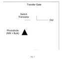
- a transfer gate (TX) or a switch transistoris formed at the same body of the nanowire structured photodetector. Additionally, the overall footprint of the photodetector plus the switch transistor is the same size as the pixel size. Therefore, a pixel according to this embodiment can be made very small.
- nanowire structured photodetectorsare formed as photodiodes in many variations including an axial p-n or p-i-n diode, a coaxial p-n or p-i-n diode.
- a transfer gate (TX)is at the same body of the nanowire structured photodetector.
- the deviceis configured to detect objects of approximately 500 nm or less in size. In another aspect, the device is configured to detect objects of approximately 100 nm or less in size.
- the nanowirecomprises silicon. In another aspect, spacing between nanowires is filled with SiO 2 . In another aspect, spacing between nanowires is filled with air or vaccuum. In another aspect, the array of pixels are arranged in a penny round pattern. In another aspect, the pixel array pattern comprises equilateral triangles.
- the active nanowire photodiodecomprises a p-i-n junction. In another aspect, the nanowire photodiode comprises a peripheral circuit element. In another aspect, the device further comprises an optical imaging system.
- the devicefurther comprises a vertical photogate and dielectric material having a refractive index lower than a refractive index of the nanowire deposited around the nanowire to form a capacitor between the vertical photogate and the nanowire.
- the vertical photogateis configured to control the potential in the nanowire, forming a potential gradient in the vertical and horizontal directions.
- each pixelcomprises a shallow trench isolation region configured to electrically isolate the pixels from each other.
- each pixelfurther comprises an indium tin oxide (ITO) layer and wherein a bias voltage is applied to the pixels through the ITO layer.
- ITOindium tin oxide
- the pixelscomprise a vertical PIN nanowire structure and a photodiode in the substrate.
- the vertical p-i-n nanowire structurecomprises an intrinsic nanowire core, a p+ layer at the top of the intrinsic nanowire core and an n ⁇ region in the substrate below the intrinsic nanowire core.
- the pixelsare configured so that a negative bias applied to the pixel depletes the nanowire of charges and generates a potential gradient in the nanowire that sweeps the charges to the substrate.
- the nanowireis further coated with a material configured to guide light down the nanowire and reduce optical crosstalk between pixels.
- the vertical p-i-n nanowire structurecomprises an n ⁇ core surrounded with an intrinsic layer, the intrinsic layer surrounded by an p+ layer.
- the pixelsare configured so that the substrate is at electrical ground and a negative bias applied to the pixels allows the nanowire and the substrate to be depleted of charges.
- the nanowireis configured with two electric filed components, one electric field component directed toward a center of the nanowire and the other directed toward the substrate. In one aspect, charges in the nanowire move toward the center of the nanowire and then toward the substrate.
- each pixelcomprises a vertical photogate and a switch placed on the nanowire photodiode.
- the array of pixelsis configured in rows and columns and the substrate is comprises an n+ layer configured to connect nanowires in a column.
- n+ layer in the substrateis configured as a signal line.
- the pixelsare configured such that when the switch is off, a potential barrier is formed underneath the switch, allowing photo-generated charges in the nanowire to accumulate.
- the nanowireis electrically isolated from the substrate but not optically isolated from the substrate. In one aspect, when the switch is turned on, charges in the nanowire flow into the substrate.
- the pixelscomprise a vertical p-i-n nanowire structure and a nanowire switch.
- the vertical p-i-n nanowire structurecomprises an intrinsic nanowire core, a p+ layer at the top of the intrinsic nanowire core and an n+ region in the substrate below the nanowire, the substrate having p doping.
- the nanowirecomprises an n ⁇ layer between the switch and the intrinsic nanowire core.
- the n+ regionhas a substantially annular shape with a hole, the hole configured to provide an electrical path from the intrinsic nanowire to the p doped substrate.
- the n+ regionhas a substantially rectangular shape.
- the vertical p-i-n nanowire structurecomprises an n ⁇ core surrounded with an intrinsic layer, the intrinsic layer surrounded by an p+ layer.
- the vertical p-i-n nanowire structurecomprises an intrinsic nanowire core, a p+ layer at the top of the intrinsic nanowire core and an n+ region in below the nanowire, wherein the n+ region is on a metal strip on an insulating layer on the substrate.
- the n+ regionhas an ohmic contact with the metal strip.
- the substratecomprises silicon, a III-V semiconductor, and II-VI semiconductor, or plastic.
- the pixelsdo not comprise a photodiode in the substrate.
- the vertical p-i-n nanowire structurecomprises an n ⁇ core surrounded with an intrinsic layer, the intrinsic layer surrounded by an p+ layer, the vertical PIN structure further comprising an n+ region in below the nanowire, wherein the n+ region is on a metal strip on an insulating layer on the substrate.
- the substratecomprises silicon, a III-V semiconductor, and II-VI semiconductor, or plastic.
- Another embodimentrelates to a method of imaging comprising obtaining a nanowire sensor array comprising an array of pixels, the pixels comprising an active nanowire photodiode and a substrate; placing an object in contact with the nanowire sensor array; exposing the object and sensor to electromagnetic radiation; and detecting an image of the object.
- the nanowire sensorcomprises at least one light source.
- the corecomprises a nanowire waveguide.
- the nanowire elementis configured to be a photodiode, a charge storage capacitor, or combinations thereof.
- the corecomprises a waveguide comprising a semiconductor material.
- the devicecould further comprise a passivation layer around the waveguide in the core.
- the devicecould further comprise a metal layer around the waveguide in the core.
- the devicecould further comprise a metal layer around the passivation layer.
- the devicecomprises no color or IR filter.
- the nanowire optical pipemay be circular, non-circular or conical.
- the devicehas a core and cladding
- the corehas a core index of refraction (n 1 )
- the devicecould further comprise at least a pair of metal contacts with at least one of the metal contacts being contacted to the nanowire waveguide.
- the nanowireis configured to separate wavelengths of an electromagnetic radiation beam incident on the nanowire waveguide at a selective wavelength through the core and the cladding without requiring a color or IR filter.
- the nanowire waveguideis configured to convert energy of the electromagnetic radiation transmitted through the waveguide and to generate electron hole pairs.
- the waveguidecomprises a p-i-n junction that is configured to detect the photo charges generated in the waveguide.
- the devicecould further comprise a lens structure or an optical coupler over the nanowire waveguide, wherein the optical coupler is operably coupled to the nanowire.
- the optical couplercomprises a curved surface to channel the electromagnetic radiation into the nanowire.
- the devicecould further comprise a stack surrounding the nanowire waveguide, the stack comprising metallic layers embedded in dielectric layers, wherein the dielectric layers have a lower refractive index than that of the cladding.
- a surface of the stackcomprises a reflective surface.
- a nanowire waveguidewhether passive or active, has a cutoff wavelength that is the lowest frequency that the waveguide can propagate.
- the diameter of the semiconductor waveguide of the coreserves as the control parameter for the cutoff wavelength of the waveguide e.
- the nanowirecould be circular in or cross section so as to function as a circular waveguide characterized by the following parameters: (1) the core radius (R e ); (2) the core index of refraction (n 1 ); and (3) the cladding index of refraction (n 2 ). These parameters generally determine the wavelength of light that can propagate through the waveguide.
- a waveguidehas a cutoff wavelength, ⁇ et . The portion of the incident electromagnetic radiation having wavelengths longer than the cutoff wavelength would not be confined with the core.
- a nanowire that functions as a waveguide whose cutoff wavelength is at greenwill not propagate blue light though the core, and a nanowire that functions as a waveguide whose cutoff wavelength is at red will not propagate blue and green light through the core.
- the corecould serve as a photodiode by absorbing the confined light and generating electron hole pairs.
- an active waveguide in the core whose cutoff wavelength is at greenwill not propagate blue light but will also absorb the confined green light and generate photo charges.
- FIG. 1shows a prior art: a cross section view of a small CMOS pixel
- FIG. 2is a schematic illustration of a pixel of an embodiment.
- FIG. 3is a schematic illustration of a pixel array of an embodiment.
- FIG. 4shows a (a) cross sectional view and (b) top view of an embodiment of pixel with a nanowire and a vertical photo gate.
- FIG. 5shows a cross sectional view of an embodiment of pixel with a vertical p-i-n nanowire photodiode and a bulk photodiode.
- FIG. 6shows a cross sectional view of an embodiment of pixel with a coaxial p-i-n nanowire photodiode.
- FIG. 7shows a (a) cross sectional view and (b) top view of an embodiment of pixel with a nanowire, a vertical photo gate and a nanowire switch transistor.
- FIG. 8shows a (a) cross sectional view and (b) top view of an embodiment of pixel with a vertical p-i-n nanowire photodiode and a nanowire switch transistor.
- FIG. 9shows a cross sectional view of an embodiment of pixel with a vertical p-i-n nanowire photodiode and a nanowire switch transistor.
- FIG. 10shows a cross sectional view of an embodiment of pixel with a coaxial p-i-n nanowire photodiode and a nanowire switch transistor.
- FIG. 11shows a cross sectional view of an embodiment of pixel with a vertical pin p-i-n nanowire photodiode and a nanowire switch on a metal strip line.
- FIG. 12shows a cross sectional view of an embodiment of a passive pixel with a coaxial p-i-n nanowire photodiode and a nanowire switch on a metal strip line.
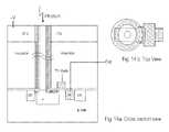
- FIG. 13shows a top view of an embodiment of an pixel array arranged in a penny round pattern.
- FIG. 14shows a (a) cross sectional view and (b) top view of an embodiment of pixel with a nanowire and a vertical photo gate and concentric dielectric layers
- FIG. 15shows a flow chart of a method according to the an embodiment.
- VPG 1(VP Gate 1) The first vertical photogate VPG 2 (VP Gate 1) The second vertical photogate TX Gate Transfer gate FD Transfer drain RG Reset gate RD Reset drain Sub Substrate VDD Positive transistor voltage Vout Output voltage NW (nw) Nanowire de Dielectric layer I (i) Current n+, n ⁇ Semiconducting material with excess donors, n+ is heavily doped, n ⁇ is lightly doped p+, p ⁇ Semiconducting material with excess acceptors, p+ is heavily doped, p ⁇ is lightly doped I Intrinsic semiconducting material ⁇ V Negative bias voltage STI Shallow trench isolation TIA Trans-impedance amplifier
- nanowirerefers to a structure that has a thickness or diameter of the order of nanometers, for example, 100 nanometers or less and an unconstrained length.
- An active nanowireis generally capable of converting photons into excitons.
- Nanowirescould include metallic (e.g., Ni, Pt, Au), semiconducting (e.g., Si, InP, GaN, etc.), and insulating (e.g., SiO 2 ,TiO 2 ) materials.
- Molecular nanowiresare composed of repeating molecular units either organic or inorganic. Nanowires could exhibit aspect ratios (length-to-width ratio) of 1000 or more. As such they could be referred to as 1-dimensional materials.
- nanowiresexamples include inorganic molecular nanowires (Mo 6 S 9-x I x , Li 2 Mo 6 Se 6 ), which could have a diameter of 0.9 nm, and can be hundreds of micrometers long.
- Other examplesare based on semiconductors such as InP, Si, GaN, etc., dielectrics (e.g. SiO 2 ,TiO 2 ), or metals (e.g. Ni, Pt).
- An active-pixel sensoralso commonly written active pixel sensor, is an image sensor consisting of an integrated circuit containing an array of pixel sensors, each pixel containing a photodetector and an active amplifier.
- a passive-pixel sensoris a pixel sensor without its own amplifier.
- excitonsrefers to electron-hole pairs.
- An active elementis any type of circuit component with the ability to electrically control electron and/or hole flow (electricity controlling electricity or light, or vice versa). Components incapable of controlling current by means of another electrical signal are called passive elements. Resistors, capacitors, inductors, transformers, and even diodes are all considered passive elements. Active elements include in embodiments disclosed herein, but are not limited to, an active nanowire, an active waveguide, transistors, silicon-controlled rectifiers (SCRs), light emitting diodes, and photodiodes.
- a waveguideis a system or material designed to confine and direct electromagnetic radiation of selective wavelengths in a direction determined by its physical boundaries.
- the selective wavelengthis a function of the diameter of the waveguide.
- An active waveguideis a waveguide that has the ability to electrically control electron and/or hole flow (electricity controlling electricity or light, or vice versa). This ability of the active waveguide, for example, is one reason why the active waveguide could be considered to be “active” and within the genus of an active element.
- An optical pipeis an element to confine and transmit an electromagnetic radiation that impinges on the optical pipe.
- the optical pipecan include a core and a cladding.
- the corecould be a nanowire.
- the optical pipecould be configured to separate wavelengths of an electromagnetic radiation beam incident on the optical pipe at a selective wavelength through the core and the cladding, wherein the core is configured to be both a channel to transmit the wavelengths up to the selective wavelength and an active element to detect the wavelengths up to the selective wavelength transmitted through the core.
- a core and a claddingare generally complimentary components of the optical pipe and are configured to separate wavelengths of an electromagnetic radiation beam incident on the optical pipe at a selective wavelength through the core and cladding.
- a photogateis a gate used in an optoelectronic device.
- the photogatecomprises a metal-oxide-semiconductor (MOS) structure.
- MOSmetal-oxide-semiconductor
- the photogatecontrols the accumulation of photo generated charges during the integration time of the photodiode and controls the transfer of charges when integration is over.
- a photodiodecomprises a pn junction, however, a photogate can be placed on any type semiconductor material.
- a vertical photogateis a new structure. Normally, photogates are placed horizontally on planar photodiode devices. In a nanowire device, however, the photogate can be formed in a vertical direction. That is, the photogate can be oriented standing up covering the lateral surface of the nanowire.
- a transfer gateis a gate of a switch transistor used in a pixel. The transfer gate's role is to transfer the charges from one side of a device to another. In some embodiments, the transfer gate is used to transfer the charges from the photodiode to the sensing node (or floating diffusion).
- a reset gateis a gate used for resetting a device. In some embodiments, the reset gate is the sense node which is formed by an n+ region. Reset means to restore to original voltage level set by a certain voltage. In some embodiments, the voltage of the reset drain (RD) is the voltage used as a reset level.
- a floating capacitoris a capacitor which floats relative to the substrate.
- a capacitorconsists of two electrodes and an insulator between them.
- both of the electrodesare connected to other devices or to signal lines.
- one of the electrodesmay not be connected to a structure.
- This unconnected, isolated areaforms the floating capacitor with respect to the substrate.
- the isolated areacomprises one electrode which is floating.
- the substratecomprises the other electrode which is normally connected to the ground.
- a depletion region between themcomprises the insulator.
- a source-follower amplifieris a common drain transistor amplifier. That is, a transistor amplifier whose source node follows the same phase as the gate node. The gate terminal of the transistor serves as the input, the source is the output, and the drain is common to both (input and output).
- a shallow layeris a doped layer that is physically located near the surface of the substrate. For example, a p+ layer may be intentionally formed very shallow by using very low energy when ion implantation is used. Normally the junction depth of a shallow layer is 0.01 ⁇ m ⁇ 0.2 ⁇ m. In contrast, a deep layer may be as deep as a few ⁇ m to tens of ⁇ m.
- An intrinsic semiconductoralso called an undoped semiconductor or i-type semiconductor, is a pure semiconductor without any significant dopant species present.
- a coreis made up of a three layers, semiconductor, insulator and metal thus forming a capacitor to collect the charge generated by the light induced carriers. Contacts are made to the metal and to the semiconductor to control and detect the stored charge.
- the corecould be formed by growing a nanowire and depositing an insulator layer and a metal layer surrounding the nanowire.
- a core having a PIN junction that induces a potential gradient in the core wirecould be formed by growing a nanowire and doping the nanowire core while it is growing as a PIN junction and contacting it at the appropriate points using the various metal layers that are part of any device.
- the photosensitive elementstypically comprise a photodiode, although not limited to only a photodiode.
- the photodiodeis doped to a concentration from about 1 ⁇ 10 16 to about 1 ⁇ 10 18 dopant atoms per cubic centimeter, while using an appropriate dopant.
- the dielectric materialsinclude as but not limited to oxides, nitrides and oxynitrides of silicon having a dielectric constant from about 4 to about 20, measured in vacuum. Also included, and also not limiting, are generally higher dielectric constant gate dielectric materials having a dielectric constant from about 20 to at least about 100. These higher dielectric constant dielectric materials may include, but are not limited to hafnium oxides, hafnium silicates, titanium oxides, barium-strontium titanates (BSTs) and lead-zirconate titanates (PZTs).
- Dielectric material-containing layersmay be formed using methods appropriate to their materials of composition.
- methodsinclude thermal or plasma oxidation or nitridation methods, chemical vapor deposition methods (including atomic layer chemical vapor deposition methods) and physical vapor deposition methods.
- the metal-containing layerscould function as electrodes.
- Non-limiting examplesinclude certain metals, metal alloys, metal silicides and metal nitrides, as well as doped polysilicon materials (i.e., having a dopant concentration from about 1 ⁇ 10 18 to about 1 ⁇ 10 22 dopant atoms per cubic centimeter) and polycide (i.e., doped polysilicon/metal silicide stack) materials.
- the metal-containing layersmay be deposited using any of several methods. Non-limiting examples include chemical vapor deposition methods (also including atomic layer chemical vapor deposition methods) and physical vapor deposition methods.
- the metal-containing layerscould comprise a doped polysilicon material (having a thickness typically in the range 1000 to 1500 Angstrom
- Individual metallization interconnection studs and metallization interconnection layers that could be used within interconnected metallization layersmay comprise any of several metallization materials that are conventional in the semiconductor fabrication art. Non-limiting examples include certain metals, metal alloys, metal nitrides and metal silicides. Most common are aluminum metallization materials and copper metallization materials, either of which often includes a barrier metallization material, as discussed in greater detail below. Types of metallization materials may differ as a function of size and location within a semiconductor structure. Smaller and lower-lying metallization features typically comprise copper containing conductor materials. Larger and upper-lying metallization features typically comprise aluminum containing conductor materials. Metallization layers typically comprise copper metallization materials and aluminum metallization materials. Other metals and alloys may be used as well.
- Dielectric and metallization layersmay be patterned using wet chemical etch methods, dry plasma etch methods or aggregate methods thereof. Dry plasma etch methods as well as e-beam etching if the dimension needs to be very small, are generally preferred insofar as they provide enhanced sidewall profile control when forming the series of patterned dielectric and metallization layers.
- the waveguiding properties of the optical pipe of the embodimentscan be improved in different ways.
- the waveguide corehas a first effective refractive index, n 1
- the material in the cladding surrounding at least a portion of the waveguidehas a second effective refractive index, n 2 , and by assuring that the first refractive index is larger than the second refractive index, n 1 >n 2 , good wave-guiding properties are provided to the optical pipe.
- the waveguiding propertiesmay be further improved by introducing optically active cladding layers on the waveguide core.
- the nanowire coreis used as a waveguide, and also as a nanostructured PD which may also be an active capacitor.
- the nanostructured PD according to the embodimentsis well suited for mass production, and the method described is scaleable for industrial use.
- the nanowire technologyoffers possibilities in choices of materials and material combinations not possible in conventional bulk layer techniques. This is utilized in the nanostructured PD according to the embodiments to provide PDs detecting light in well defined wavelength regions not possible by conventional technique.
- the design according to the embodimentsallows for inclusions of heterostructures as well as areas of different doping within the nanowire, facilitating optimization of electrical and/or optical properties.
- the waveguiding properties of the optical pipe of the embodimentscan be improved in different ways.
- the waveguide corehas a first effective refractive index, n 1
- the material in the cladding surrounding at least a portion of the waveguidehas a second effective refractive index, n 2 , and by assuring that the first refractive index is larger than the second refractive index, n 1 >n 2 , good wave-guiding properties are provided to the optical pipe.
- the waveguiding propertiesmay be further improved by introducing optically active cladding layers on the waveguide core.
- the nanowire coreis used as a waveguide, and also as a nanostructured PD which may also be an active capacitor.
- the nanostructured PD according to the embodimentsis well suited for mass production, and the method described is scaleable for industrial use.
- a nanostructured PDcomprises of an upstanding nanowire.
- an upstanding nanowireshould be interpreted as a nanowire protruding from the substrate in some angle, the upstanding nanowire for example being grown from the substrate, preferably by as vapor-liquid-solid (VLS) grown nanowires.
- VLSvapor-liquid-solid
- the angle with the substratewill typically be a result of the materials in the substrate and the nanowire, the surface of the substrate and growth conditions. By controlling these parameters it is possible to produce nanowires pointing in only one direction, for example vertical, or in a limited set of directions.
- nanowires and substrates of zinc-blende and diamond semiconductors composed of elements from columns III, V and IV of the periodic tablecan be grown in the [111] directions and then be grown in the normal direction to any ⁇ 111 ⁇ substrate surface.
- Other directions given as the angle between normal to the surface and the axial direction of the nanowireinclude 70.53° ⁇ 111 ⁇ , 54.73° ⁇ 100 ⁇ , and 35.27° and 90°, both to ⁇ 110 ⁇ .
- the nanowiresdefine one, or a limited set, of directions.
- the ability to grow nanowires with well defined diametersis in one embodiment utilized to optimize the waveguiding properties of the nanowire or at least the waveguide with regards to the wavelength of the light confined and converted by the nanostructured PD.
- the diameter of the nanowireis chosen so as to have a favorable correspondence to the wavelength of the desired light.
- the dimensions of the nanowireare such that a uniform optical cavity, optimized for the specific wavelength of the produced light, is provided along the nanowire.
- the core nanowiremust be sufficiently wide to capture the desired light.
- a rule of thumbwould be that diameter must be larger than ⁇ /2 w , wherein ⁇ is the wavelength of the desired light and n w is the refractive index of the nanowire.
- a diameter of about 60 nmmay be appropriate to confine blue light only and one 80 nm may be appropriate for to confine both blue and green light only in a silicon nanowire.
- a diameter of 45 nmmay be appropriate to confine UV light.
- the silicon nanowire of the embodiments disclosed hereincould be made as follows.
- a substrateis provided which comprises silicon having a silicon dioxide surface.
- the surfacecan be modified with a surface treatment to promote adsorption of a gold nanoparticle.
- the gold nanoparticlecan be formed by deposition of a gold layer, followed by removal of the gold layer over regions other than desired location of the gold nanoparticle.
- the gold nanoparticlecan be surface treated to provide for steric stabilization.
- tethered, sterically stabilized gold nanoparticlescan be used as seeds for further synthesis of nanowires, wherein the gold nanoparticles are adsorbed to the modified silicon substrate.
- DPSdiphenyl silane
- the silicon atomsattach to the gold nanoparticle and a silicon nanowire crystallizes from the gold nanoparticle seed upon saturation of the gold nanoparticle with silicon atoms. Note that the thickness and diameter of the gold particle left behind on the back-side surface determines the diameter of the nanowire.
- a silicon nanowirecan be grown, for example, by plasma enhanced vapor-liquid-solid growth.
- Other methods of growing silicon nanowirecould employ the vapor-liquid-solid (VLS) growth mechanism.
- the nanowirescould also be epitaxially grown Si-NWs synthesized by the VLS growth mechanism using silicon tetrachloride (SiCl 4 ) as precursor gas, requiring temperatures beyond 800° C.
- SiCl 4silicon tetrachloride
- the gaseous hydrochloric acid, a byproduct of SiCl 4 decomposition in the reaction tubecould etch the oxide layer on the Si surface, creating a clean Si crystal surface for epitaxial NW growth.
- Epitaxial siliconcould also be grown selectively by intentionally introducing HCl into the SiH 4 /H 2 system.
- Epitaxial growth of Si-NWsmay be accomplished using a gallium/gold (Ga/Au)-nanoparticle-catalyzed chemical vapor deposition (CVD) of SiH 4 on Si (111) and Si (100) surfaces.
- Ga/Augallium/gold
- CVDchemical vapor deposition
- the silicon nanowire of the embodiments disclosed hereincould be made as follows.
- a substrateis provided which comprises silicon having a silicon dioxide surface.
- the surfacecan be modified to remove an oxide layer with a surface treatment to promote adsorption of a gold nanoparticle, or gold alloys nanoparticle like AuGa.
- a Si substratepreferably have the ⁇ 111 ⁇ plane, (Au is used to create the Si—Au eutectic point and grow the Si nanowire when SiH4 is introduced), the gold nanoparticle can be formed by deposition of a gold layer, followed by removal of the gold layer over regions other than desired location of the gold nanoparticle.
- the silicon nanowirecan be grown, for example, by plasma enhanced vapor-liquid-solid growth.
- a catalyst particletypically gold or gold alloy
- EBLelectron beam lithography
- Other processes for depositing catalysts, such as electroless platingmay also be used.
- the diameters of nanowires after growthare generally determined by the area of the catalyst particles. Therefore, a desired diameter of the nanowire can be synthesized by depositing a catalyst particle with an appropriate size. This step typically determines the functionality of the nanowire pixel because the nanowire diameter should be of an appropriate cross-section area to allow the transmission of light with specific wavelengths and long enough to allow the light absorption and creation of excitons (electron-hole pairs).
- a single nanowirecan be grown from the catalyst particle under proper conditions.
- a suitable nanowirecan be grown using the vapor-liquid-solid (VLS) process with presence of SiH 4 at, for example, temperature at 650 C and pressure of 200 mTorr.
- VLSvapor-liquid-solid
- a temperature below 450 Cis advisable for the integration compatibility of CMOS circuits and nanowire synthesis.
- Many researchershave been able to synthesize silicon nanowires at 430 C or even below 400 C by using some special techniques, for example, using aluminum catalysts or plasma enhanced growth.
- the silicon nanowirecan be doped to create a p + -i(intrinsic)-n + structure by introducing B 2 H 6 , H 2 and PH 3 , respectively.
- Nanowireshave a higher surface-to-volume ratio than the corresponding bulk materials. Therefore the surface states of nanowires play a more important role in their electronic and optical properties. The impact of nanowire surface states, however, can be minimized by surface passivation after the nanowire synthesis.
- surface passivationcan be achieved with a monolayer of materials to react with silicon dangling bonds at the surface of the nanowire. This is accomplished with the formation of stable bonds after reaction.
- passivationhas almost no effect on the nanowire physical dimension since it is only one-monolayer thick.
- Subsequent stepscould relate to the forming of an epitaxial layer that is n or p doped covering the nanowire or of one or more of the dielectric layers around the nanowire.
- the epitaxial n or p doped layer covering the nanowirecould be grown using vapor-phase epitaxy (VPE), a modification of chemical vapor deposition.
- VPEvapor-phase epitaxy
- MBE and LPEliquid-phase epitaxy
- SPEsolid-phase epitaxy
- a dopantcould be added into the epitaxially grown layer during the epitaxial layer growth process.
- a conformal dielectric coating around the nanowirecould be made by chemical vapor deposition (CVD), atomic layer deposition (ALD), oxidation or nitration could be made around the nanowire.
- CVDchemical vapor deposition
- ALDatomic layer deposition
- oxidation or nitrationcould be made around the nanowire.
- doped glass dielectric layercould be formed on the conformal dielectric coating by plasma enhanced chemical vapor deposition, spin-on coating or sputtering, optionally with an initial atomic layer deposition.
- the deposited doped glass dielectric layercould be etched back by chemical-mechanical planarization or other methods of etching.
- FIG. 2is a schematic illustration of a passive pixel according to an embodiment.
- the passive pixel according to this embodimentincludes a photodiode and a switch transistor. When photon energy is absorbed in a photodiode, electron and hole charges are generated. Among the electrons and holes the minority charge carriers are integrated in the potential well formed in the photodiode. The integration of the minority charges continues until a switch transistor is turned on.
- the transfer gatecauses the integrated charges to dump into the output node.
- the output signalis in the form of current flow that flows for a short period of time. The time period is short because the amount of charge stored in the photodiode is limited.
- FIG. 3illustrates a simplified passive pixel array device block diagram.
- the passive pixel arrayincludes m ⁇ n pixels.
- the arraymay include n rows and m columns, where m and n are different.
- each pixel output in a columnis connected to a column signal bus.
- each column signal busis connected to the input of a trans-impedance amplifier (TIA).
- TIAtrans-impedance amplifier
- the TIAconverts the photocurrent signal into a voltage signal.
- each transfer gate in a rowis connected to a single bus line which is driven by a vertical driver.
- a transfer gate driverenables Y 1 so that the pixel group in the first row can be enabled to dump the charges in the first row to the column signal bus.
- the TIAconverts the current signal into a voltage signal.
- Y 1is disabled.
- Y 2is enabled. This process repeats until the pixel group in the last row is enabled by Yn. In this way, the m ⁇ n pixel array is scanned in a vertical direction. In the horizontal direction, each output of the TIA's may be scanned using a multiplex switch array (not shown).
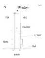
- FIG. 4illustrates a (a) cross sectional view and (b) top view of an embodiment of pixel with a nanowire and a vertical photo gate.
- this embodimentthere are two photodiode components, a nanowire photodiode and bulk or substrate photodiode. Photons are absorbed in the n ⁇ nanowire and n ⁇ bulk diode. The pixel of this embodiment, however, can not separate the signals between two photodiodes.
- the nanowire and bulk photodiodescomprise n ⁇ doped regions which allow easy depletion in a reversed bias condition.
- a reversed bias conditionmay be set up by applying a negative voltage ( ⁇ V) with a vertical photo gate and a ground bias at the substrate.
- ⁇ Vnegative voltage
- the n+ output nodeis normally positively biased. This typically helps to deplete the n ⁇ regions further.
- the p+ regions surrounding the nanowire edgesserve to suppress the leakage current generated during the integration. Leakage current is typically generated due to the surface defect which exist near the edges and surface of the bulk photodiode area.
- a dielectric material whose refractive index is lower than the core material of the nanowireis deposited to form a capacitor between the vertical photogate (VPG) and the nanowire.
- the dielectric layeralso helps guide the light beam toward the bulk diode.
- the pixelalso includes a shallow trench isolation (STI).
- STIshallow trench isolation
- CMOScomplementary metal-oxide-semiconductor
- LOCOSLocal Oxidation of Silicon
- a vertical photo gate (VPG) biasis applied through an indium-tin-oxide (ITO) layer comprising the top of the pixel.
- ITOindium-tin-oxide
- the VPGserves two functions. First, the VPG may be used to control the potential in the nanowire. This enables a potential gradient to form in the nanowire in both the vertical direction and the horizontal direction. Second, the VPG allows the nanowire and the bulk photodiodes to deplete.
- the ITO layerserves as a conductive layer to supply the bias voltage to the VPG.
- the deposition process temperature of ITOis relatively low (typically 200 C ⁇ 400 C). The low deposition temperature helps prevent damage of the CMOS devices that have already been fabricated in the substrate. ITO has a further advantage in that it is optically transparent.
- FIG. 5illustrates an embodiment of pixel with a vertical pin nanowire and a bulk photodiode.
- This embodimentincludes two photodiode components.
- the nanowire photodiodeis formed as a vertical p-i-n diode. It has a p+ layer at the top of the nanowire and an n ⁇ region at the bottom (in the substrate).
- the rest of the nanowireis coated with a dielectric material, typically an oxide material.
- the resulting structuremay then be surrounded with a metal or conductor material so that light can be guided down the nanowire without causing optical crosstalk between the neighboring nanowire's.
- the n ⁇ regionfunctions as the bulk diode. That is, the n ⁇ region absorbs the light coming though the nanowire.
- a negative biaswhich is denoted by ⁇ V, depletes the intrinsic (undoped) nanowire and the n ⁇ region. Further, a vertical electrical field is generated in the nanowire. The vertical electric field in the intrinsic region of the nanowire sweeps the photo generated charges toward the n ⁇ region where the potential well is located.
- FIG. 6illustrates an embodiment of pixel with a coaxial p-i-n nanowire.
- the nanowire photodiodeis formed as a coaxial or concentric p-i-n diode. It has p+ at the outer shell and n ⁇ at the core and an intrinsic layer sandwiched between.
- a negative biaswhich is denoted by ⁇ V, is applied to the p+ layer through the ITO layer.
- the p ⁇ substrateis ground (OV) biased so that the intrinsic layer, the n ⁇ region of the nanowire and the n ⁇ region in the bulk can be depleted.
- the n+ output nodeis normally positively biased. This helps to further deplete the n ⁇ regions.
- the coaxial nanowirethere are two electric field components in the coaxial nanowire.
- One componentis an electric field directed toward the center of the nanowire.
- the otheris directed in downward direction. That is, toward the substrate.
- There are two electric field componentsbecause the n ⁇ region in the core of the nanowire has a lower resistivity than that of the intrinsic layer. In the extreme case of an insulator which has an infinite resistivity, the highest electric field component would be between the two electrodes. That is, toward the center of the nanowire in the configuration of this embodiment.
- the vertical electric field componentis established even if the potential gradient is not steep. This is because the nanowire is long and the substrate is connected to ground.
- Deposition of the intrinsic layer and the p+ layercan be done by employing atomic layer deposition (ALD) or chemical vapor deposition (CVD) process technology.
- ALDatomic layer deposition
- CVDchemical vapor deposition
- FIG. 7illustrates a (a) cross sectional view and (b) top view of an embodiment of pixel with a nanowire, a vertical photo gate and a nanowire switch transistor.
- a switch transistoris formed in the nanowire. Since both the photodiode and the switch transistor are placed in the same nanowire which is standing up vertically, its footprint is the same size as the pixel size. Therefore, a pixel according to this embodiment can be made very small.
- this embodimentincludes an n+ layer in the form of a stripe in the vertical (column) direction of the pixel array. Since the n+ layer has a low resistivity, a signal line can be made without using any additional metal lines. This will typically simplify the device fabrication of this embodiment.
- the GateWhen the Gate is off, a potential barrier is formed underneath the Gate so that photo generated charges can be integrated in the nanowire without the charges moving into the n+ region in the substrate.
- the GateWhen the Gate is turned off, the nanowire is electrically isolated from the substrate. The nanowire, however, is not optically isolated from the substrate. Therefore, light can reach the n+ region and the substrate p-sub, generating charges at the bottom (substrate) diode.
- Charges generated in the bulk diodecan not be used, however, because the n+ region is shared with pixel ground in a column of the array. Therefore, before reading out the nanowire signal, it is necessary to rest the n+ region. Reset can be accomplished by the reset operation of the TIA located at each column.
- the GateWhen the Gate is turned on, integrated charges in the nanowire are dumped into the n+ region because the potential barrier may be removed by applying an appropriate bias voltage to the Gate. The TIA then converts the current signal from the pixel charge flow into a voltage signal.
- FIG. 8shows a (a) cross sectional view and (b) top view of an embodiment of pixel with a vertical p-i-n nanowire photodiode and a nanowire switch transistor.
- the nanowirehas a vertical p-i-n structure with a p+ layer at the top portion of the nanowire and n+ and n ⁇ layers at the bottom.
- a potential barrieris formed underneath the Gate so that photo generated charges can be integrated in the nanowire without moving into the n+ region at the bottom of the nanowire.
- chargesare collected in the n ⁇ layer above the Gate because the n ⁇ layer is the place where the lowest potential (highest voltage) exists. This is because charges have a tendency to go to the place where the potential is lowest. If the nanowire did not have an n ⁇ layer, the collection area for the charge would not be well defined.
- FIG. 8 billustrates that shape of the n+ layer.
- the reason for the hole in the circular shapeis to provide a path from the substrate p-sub to the intrinsic nanowire. This helps build a potential barrier underneath the Gate because a reverse bias may be supplied from the p-sub.
- FIG. 9shows a cross sectional view of an embodiment of pixel with a vertical p-i-n nanowire photodiode and a nanowire switch transistor. Everything in this embodiment is the same as the embodiment illustrated in FIG. 8 a except shape of the n+ region. In this embodiment, the n+ regions has a simple stripe without the additional annular pattern.
- FIG. 10shows a cross sectional view of an embodiment of pixel with a coaxial p-i-n nanowire photodiode and a nanowire switch transistor.
- the nanowirehas a coaxial or concentric shaped p-i-n structure. That is, the nanowire has a p+ layer at the outer shell and an n ⁇ region in the core with an intrinsic layer sandwiched between the two.
- a potential barrieris formed underneath the Gate. Photo generated charges can be integrated in the nanowire without moving into the n+ region at the bottom.
- the coaxial p-i-n structurehelps improve the charge transfer without experiencing trapping due to surface defects in the nanowire. This is because the electric field directed toward the core results in a charge transfer path to the core of the nanowire.
- FIG. 11shows a cross sectional view of an embodiment of pixel with a vertical pin nanowire and a nanowire switch on a metal strip line.
- the nanowireis formed on top a metal stripe which is placed on the insulated substrate.
- an n+ materialwhich has a ⁇ 111> orientation is either deposited or is bonded so as to have an ohmic contact with metal.
- an intrinsic type nanowireis formed.
- the top portion of the nanowireis coated with a p+ doped material so that a vertical p-i-n diode can be formed.
- a negative bias voltagemay be applied to the p+ layer through the ITO layer.
- the bottom metal stripemay be biased positively through a TIA. This causes a reverse bias which results in the nanowire being depleted.
- the operation of the pixel of this embodimentis same as the structure shown in FIG. 9 .
- This structurehas several advantages over that embodiment.
- the substrateneed not be silicon.
- the substratemay be, for example, a III-V semiconductor, a II-VI semiconductor, or a plastic.
- the substratemay be any material which is capable of providing mechanical support for the pixels. That is, because the substrate is electrically isolated from the pixels, the substrate does not have to be able to conduct electricity.
- the nanowire and the substratecan comprise different materials.
- the substratecan comprise silicon while the nanowire can comprise a III-V or II-IV material.
- n+ layerSince there is no bulk diode, it is unnecessary to reset the n+ diode if the n+ layer is very thin. In other words, even without a bulk diode, the n+ layer on top of the metal becomes a parasitic bulk diode. If the thickness of the n+ layer is small, charge generation in n+ layer can be negligibly small.
- FIG. 12shows a cross sectional view of an embodiment of a passive pixel with a coaxial p-i-n nanowire photodiode and a nanowire switch on a metal strip line. Everything in this embodiment is the same as in the embodiment illustrate in FIG. 11 , except this embodiment has a coaxial p-i-n nanowire structure.
- FIG. 13illustrates an embodiment of a sensor array.
- FIG. 13illustrates a penny round pattern where the pixels are arranged as a staggered pattern row by row.
- Other ways of arranging the pixel arraymay also be used. Examples include, but are not limited to, hexagonal pattern, Bayer pattern, and semi-regular pattern.
- Individual nanowire sensorsare preferably located at the center of each pixel. By placing the nanowire sensors in a close-packed configuration, a high density array of sensors can be produced.
- FIGS. 14 a and 14 billustrates an embodiment of a passive pixel which is similar to the embodiment illustrated in FIG. 4 , however, in this embodiment the nanowire is surrounded by two or more concentric dielectric layers.
- the nanowirelacks a concentric metal layer.
- the nanowireis surrounded by two or more concentric dielectric layers and a concentric metal layer.
- the two or more concentric dielectric layersperform the light guiding function performed by the metal in the embodiment illustrated in FIG. 5 .
- one aspect of this embodimentis the absence of a metal layer.
- the successive concentric dielectric layers of the two or more concentric dielectric layershave a lower index of refraction with increasing radius. That is, concentric dielectric layers with a larger radius have a lower index of refraction than concentric dielectric layers having a smaller radius. In another aspect, adjacent concentric dielectric layers have alternating higher and lower indexes of refraction. All references mentioned in the application are incorporated herein in their entirety by reference.
- a signal bearing mediumexamples include, but are not limited to, the following: a recordable type medium such as a floppy disk, a hard disk drive, a Compact Disc (CD), a Digital Video Disk (DVD), a digital tape, a computer memory, etc.; and a transmission type medium such as a digital and/or an analog communication medium (e.g., a fiber optic cable, a waveguide, a wired communications link, a wireless communication link, etc.).
- a typical data processing systemgenerally includes one or more of a system unit housing, a video display device, a memory such as volatile and non-volatile memory, processors such as microprocessors and digital signal processors, computational entities such as operating systems, drivers, graphical user interfaces, and applications programs, one or more interaction devices, such as a touch pad or screen, and/or control systems including feedback loops and control motors (e.g., feedback for sensing position and/or velocity; control motors for moving and/or adjusting components and/or quantities).
- a typical data processing systemmay be implemented utilizing any suitable commercially available components, such as those typically found in data computing/communication and/or network computing/communication systems.
- any two components so associatedcan also be viewed as being “operably connected,” or “operably coupled,” to each other to achieve the desired functionality, and any two components capable of being so associated can also be viewed as being “operably couplable,” to each other to achieve the desired functionality.
- operably couplableinclude but are not limited to optical coupling to permit transmission of optical light, for example via an optical pipe or fiber, physically interacting components and/or wirelessly interactable and/or wirelessly interacting components and/or logically interacting and/or logically interactable components.
Landscapes
- Solid State Image Pick-Up Elements (AREA)
- Light Receiving Elements (AREA)
Abstract
Description
| Symbol | Element |
| VPG 1 (VP Gate 1) | The first vertical photogate |
| VPG 2 (VP Gate 1) | The second vertical photogate |
| TX Gate | Transfer gate |
| FD | Transfer drain |
| RG | Reset gate |
| RD | Reset drain |
| Sub | Substrate |
| VDD | Positive transistor voltage |
| Vout | Output voltage |
| NW (nw) | Nanowire |
| de | Dielectric layer |
| I (i) | Current |
| n+, n− | Semiconducting material with excess donors, |
| n+ is heavily doped, n− is lightly doped | |
| p+, p− | Semiconducting material with excess |
| acceptors, p+ is heavily doped, p− is | |
| lightly doped | |
| I | Intrinsic semiconducting material |
| −V | Negative bias voltage |
| STI | Shallow trench isolation |
| TIA | Trans-impedance amplifier |
Claims (64)
Priority Applications (19)
| Application Number | Priority Date | Filing Date | Title |
|---|---|---|---|
| US12/575,221US8384007B2 (en) | 2009-10-07 | 2009-10-07 | Nano wire based passive pixel image sensor |
| PCT/US2010/051446WO2011044108A1 (en) | 2009-10-07 | 2010-10-05 | Nano wire based passive pixel image sensor |
| CN201080043180.1ACN102576643B (en) | 2009-10-07 | 2010-10-05 | Nanowire-based passive pixel image sensor |
| TW099134252ATWI435444B (en) | 2009-10-07 | 2010-10-07 | Passive pixel image sensor based on nanowire |
| US12/945,492US9515218B2 (en) | 2008-09-04 | 2010-11-12 | Vertical pillar structured photovoltaic devices with mirrors and optical claddings |
| US13/106,851US9082673B2 (en) | 2009-10-05 | 2011-05-12 | Passivated upstanding nanostructures and methods of making the same |
| US13/925,429US9304035B2 (en) | 2008-09-04 | 2013-06-24 | Vertical waveguides with various functionality on integrated circuits |
| US14/503,598US9410843B2 (en) | 2008-09-04 | 2014-10-01 | Nanowire arrays comprising fluorescent nanowires and substrate |
| US14/516,162US20160111562A1 (en) | 2008-09-04 | 2014-10-16 | Multispectral and polarization-selective detector |
| US14/516,402US20160111460A1 (en) | 2008-09-04 | 2014-10-16 | Back-lit photodetector |
| US14/632,739US9601529B2 (en) | 2008-09-04 | 2015-02-26 | Light absorption and filtering properties of vertically oriented semiconductor nano wires |
| US14/704,143US20150303333A1 (en) | 2008-09-04 | 2015-05-05 | Passivated upstanding nanostructures and methods of making the same |
| US14/705,380US9337220B2 (en) | 2008-09-04 | 2015-05-06 | Solar blind ultra violet (UV) detector and fabrication methods of the same |
| US15/057,153US20160178840A1 (en) | 2008-09-04 | 2016-03-01 | Optical waveguides in image sensors |
| US15/082,514US20160211394A1 (en) | 2008-11-13 | 2016-03-28 | Nano wire array based solar energy harvesting device |
| US15/090,155US20160216523A1 (en) | 2008-09-04 | 2016-04-04 | Vertical waveguides with various functionality on integrated circuits |
| US15/093,928US20160225811A1 (en) | 2008-09-04 | 2016-04-08 | Nanowire structured color filter arrays and fabrication method of the same |
| US15/149,252US20160254301A1 (en) | 2008-09-04 | 2016-05-09 | Solar blind ultra violet (uv) detector and fabrication methods of the same |
| US15/225,264US20160344964A1 (en) | 2008-09-04 | 2016-08-01 | Methods for fabricating and using nanowires |
Applications Claiming Priority (1)
| Application Number | Priority Date | Filing Date | Title |
|---|---|---|---|
| US12/575,221US8384007B2 (en) | 2009-10-07 | 2009-10-07 | Nano wire based passive pixel image sensor |
Related Parent Applications (2)
| Application Number | Title | Priority Date | Filing Date |
|---|---|---|---|
| US12/573,582Continuation-In-PartUS8791470B2 (en) | 2008-09-04 | 2009-10-05 | Nano structured LEDs |
| US12/633,323Continuation-In-PartUS8735797B2 (en) | 2008-09-04 | 2009-12-08 | Nanowire photo-detector grown on a back-side illuminated image sensor |
Related Child Applications (2)
| Application Number | Title | Priority Date | Filing Date |
|---|---|---|---|
| US12/573,582Continuation-In-PartUS8791470B2 (en) | 2008-09-04 | 2009-10-05 | Nano structured LEDs |
| US12/633,323Continuation-In-PartUS8735797B2 (en) | 2008-09-04 | 2009-12-08 | Nanowire photo-detector grown on a back-side illuminated image sensor |
Publications (2)
| Publication Number | Publication Date |
|---|---|
| US20110079704A1 US20110079704A1 (en) | 2011-04-07 |
| US8384007B2true US8384007B2 (en) | 2013-02-26 |
Family
ID=43822464
Family Applications (1)
| Application Number | Title | Priority Date | Filing Date |
|---|---|---|---|
| US12/575,221Expired - Fee RelatedUS8384007B2 (en) | 2008-09-04 | 2009-10-07 | Nano wire based passive pixel image sensor |
Country Status (4)
| Country | Link |
|---|---|
| US (1) | US8384007B2 (en) |
| CN (1) | CN102576643B (en) |
| TW (1) | TWI435444B (en) |
| WO (1) | WO2011044108A1 (en) |
Cited By (25)
| Publication number | Priority date | Publication date | Assignee | Title |
|---|---|---|---|---|
| US20100148221A1 (en)* | 2008-11-13 | 2010-06-17 | Zena Technologies, Inc. | Vertical photogate (vpg) pixel structure with nanowires |
| US20110133061A1 (en)* | 2009-12-08 | 2011-06-09 | Zena Technologies, Inc. | Nanowire photo-detector grown on a back-side illuminated image sensor |
| US8514411B2 (en) | 2009-05-26 | 2013-08-20 | Zena Technologies, Inc. | Determination of optimal diameters for nanowires |
| US8546742B2 (en) | 2009-06-04 | 2013-10-01 | Zena Technologies, Inc. | Array of nanowires in a single cavity with anti-reflective coating on substrate |
| US8710488B2 (en) | 2009-12-08 | 2014-04-29 | Zena Technologies, Inc. | Nanowire structured photodiode with a surrounding epitaxially grown P or N layer |
| US8748799B2 (en) | 2010-12-14 | 2014-06-10 | Zena Technologies, Inc. | Full color single pixel including doublet or quadruplet si nanowires for image sensors |
| US8766272B2 (en) | 2009-12-08 | 2014-07-01 | Zena Technologies, Inc. | Active pixel sensor with nanowire structured photodetectors |
| US8791470B2 (en) | 2009-10-05 | 2014-07-29 | Zena Technologies, Inc. | Nano structured LEDs |
| US8835905B2 (en) | 2010-06-22 | 2014-09-16 | Zena Technologies, Inc. | Solar blind ultra violet (UV) detector and fabrication methods of the same |
| US8866065B2 (en) | 2010-12-13 | 2014-10-21 | Zena Technologies, Inc. | Nanowire arrays comprising fluorescent nanowires |
| US8889455B2 (en) | 2009-12-08 | 2014-11-18 | Zena Technologies, Inc. | Manufacturing nanowire photo-detector grown on a back-side illuminated image sensor |
| US8890271B2 (en) | 2010-06-30 | 2014-11-18 | Zena Technologies, Inc. | Silicon nitride light pipes for image sensors |
| US9000353B2 (en) | 2010-06-22 | 2015-04-07 | President And Fellows Of Harvard College | Light absorption and filtering properties of vertically oriented semiconductor nano wires |
| US9082673B2 (en) | 2009-10-05 | 2015-07-14 | Zena Technologies, Inc. | Passivated upstanding nanostructures and methods of making the same |
| US9299866B2 (en) | 2010-12-30 | 2016-03-29 | Zena Technologies, Inc. | Nanowire array based solar energy harvesting device |
| US9304035B2 (en) | 2008-09-04 | 2016-04-05 | Zena Technologies, Inc. | Vertical waveguides with various functionality on integrated circuits |
| US20160111460A1 (en)* | 2008-09-04 | 2016-04-21 | Zena Technologies, Inc. | Back-lit photodetector |
| US9343490B2 (en) | 2013-08-09 | 2016-05-17 | Zena Technologies, Inc. | Nanowire structured color filter arrays and fabrication method of the same |
| US9406709B2 (en) | 2010-06-22 | 2016-08-02 | President And Fellows Of Harvard College | Methods for fabricating and using nanowires |
| US9429723B2 (en) | 2008-09-04 | 2016-08-30 | Zena Technologies, Inc. | Optical waveguides in image sensors |
| US9478685B2 (en) | 2014-06-23 | 2016-10-25 | Zena Technologies, Inc. | Vertical pillar structured infrared detector and fabrication method for the same |
| US9515218B2 (en) | 2008-09-04 | 2016-12-06 | Zena Technologies, Inc. | Vertical pillar structured photovoltaic devices with mirrors and optical claddings |
| US10056513B2 (en) | 2016-02-12 | 2018-08-21 | Nokia Technologies Oy | Apparatus and method of forming an apparatus comprising a two dimensional material |
| US20190326270A1 (en)* | 2013-09-30 | 2019-10-24 | Aledia | Opto-electronic device with light-emitting diodes |
| US11742370B2 (en) | 2020-05-27 | 2023-08-29 | Microsoft Technology Licensing, Llc | Time-of-flight pixel with vertical photogates |
Families Citing this family (16)
| Publication number | Priority date | Publication date | Assignee | Title |
|---|---|---|---|---|
| US8390705B2 (en)* | 2009-10-27 | 2013-03-05 | Hewlett-Packard Develoment Company, L.P. | Nanowire photodiodes |
| EP2933629B1 (en) | 2010-02-19 | 2019-04-10 | Pacific Biosciences Of California, Inc. | System for measuring analytical reactions comprising a socket for an optode array chip |
| JP5709546B2 (en)* | 2011-01-19 | 2015-04-30 | キヤノン株式会社 | Energy beam drawing apparatus and device manufacturing method |
| US20130187051A1 (en)* | 2011-10-06 | 2013-07-25 | Massachusetts Institute Of Technology | Frequency multiplexed superconducting nanowire photon detectors |
| CN103959363B (en)* | 2011-12-07 | 2016-04-27 | 夏普株式会社 | The method of operating of optical sensor circuit and possess the method for operating of display device of this optical sensor circuit |
| US8901697B2 (en)* | 2012-03-16 | 2014-12-02 | Analog Devices, Inc. | Integrated circuit having a semiconducting via; an integrated circuit including a sensor, such as a photosensitive device, and a method of making said integrated circuit |
| CN102969326B (en)* | 2012-12-05 | 2015-04-01 | 中国科学院上海高等研究院 | Image sensor and preparation method thereof |
| JP2015106621A (en)* | 2013-11-29 | 2015-06-08 | ソニー株式会社 | Solid-state imaging device, manufacturing method, and electronic apparatus |
| KR20150104420A (en)* | 2014-03-05 | 2015-09-15 | 삼성전자주식회사 | Semiconductor device and method of fabricating the same |
| CN104134675A (en)* | 2014-07-16 | 2014-11-05 | 上海集成电路研发中心有限公司 | Color and gray image sensor for improving utilization rate of incident light |
| CN114691585B (en) | 2015-05-07 | 2023-10-13 | 加利福尼亚太平洋生物科学股份有限公司 | Multiprocessor pipeline architecture |
| US10056439B2 (en) | 2015-12-11 | 2018-08-21 | Gingy Technologies Inc. | Image capturing apparatus |
| KR102667265B1 (en) | 2017-01-03 | 2024-05-21 | 삼성전자주식회사 | Image sensor comprising nano antenna |
| TWI653583B (en)* | 2017-07-17 | 2019-03-11 | Gingy Technology Inc. | Image capture device |
| KR20220103537A (en) | 2021-01-15 | 2022-07-22 | 삼성전자주식회사 | Optical isolator and photonic integrated circuit including the same |
| TWM624315U (en)* | 2021-03-18 | 2022-03-11 | 神盾股份有限公司 | Light sensing module |
Citations (230)
| Publication number | Priority date | Publication date | Assignee | Title |
|---|---|---|---|---|
| US1918848A (en) | 1929-04-26 | 1933-07-18 | Norwich Res Inc | Polarizing refracting bodies |
| US4017332A (en) | 1975-02-27 | 1977-04-12 | Varian Associates | Solar cells employing stacked opposite conductivity layers |
| US4827335A (en) | 1986-08-29 | 1989-05-02 | Kabushiki Kaisha Toshiba | Color image reading apparatus with two color separation filters each having two filter elements |
| US4880613A (en) | 1987-01-12 | 1989-11-14 | Sumitomo Electric Industries, Ltd. | Light emitting element comprising diamond and method for producing the same |
| US4896941A (en) | 1985-04-27 | 1990-01-30 | Doryokuro Kakunenryo Kaihatsu Jigyodan | Image-transmitting fiber |
| US4950625A (en) | 1988-06-13 | 1990-08-21 | Sumitomo Electric Industries, Ltd. | Diamond laser crystal and method manufacturing the same |
| US4971928A (en) | 1990-01-16 | 1990-11-20 | General Motors Corporation | Method of making a light emitting semiconductor having a rear reflecting surface |
| US4972244A (en) | 1988-06-16 | 1990-11-20 | Commissariat A L'energie Atomique | Photodiode and photodiode array on a II-VI material and processes for the production thereof |
| US5096520A (en) | 1990-08-01 | 1992-03-17 | Faris Sades M | Method for producing high efficiency polarizing filters |
| US5124543A (en) | 1989-08-09 | 1992-06-23 | Ricoh Company, Ltd. | Light emitting element, image sensor and light receiving element with linearly varying waveguide index |
| US5272518A (en) | 1990-12-17 | 1993-12-21 | Hewlett-Packard Company | Colorimeter and calibration system |
| US5311047A (en) | 1988-11-16 | 1994-05-10 | National Science Council | Amorphous SI/SIC heterojunction color-sensitive phototransistor |
| US5347147A (en) | 1990-11-28 | 1994-09-13 | Jones Barbara L | Light emitting diamond device |
| US5362972A (en) | 1990-04-20 | 1994-11-08 | Hitachi, Ltd. | Semiconductor device using whiskers |
| US5401968A (en) | 1989-12-29 | 1995-03-28 | Honeywell Inc. | Binary optical microlens detector array |
| US5449626A (en) | 1991-12-27 | 1995-09-12 | Hezel; Rudolf | Method for manufacture of a solar cell |
| US5602661A (en) | 1993-02-17 | 1997-02-11 | Hoffmann-La Roche Inc. | Optical component |
| US5612780A (en) | 1996-06-05 | 1997-03-18 | Harris Corporation | Device for detecting light emission from optical fiber |
| US5723945A (en) | 1996-04-09 | 1998-03-03 | Electro Plasma, Inc. | Flat-panel display |
| US5747796A (en) | 1995-07-13 | 1998-05-05 | Sharp Kabushiki Kaisha | Waveguide type compact optical scanner and manufacturing method thereof |
| US5767507A (en) | 1996-07-15 | 1998-06-16 | Trustees Of Boston University | Polarization sensitive photodetectors and detector arrays |
| US5798535A (en) | 1996-12-20 | 1998-08-25 | Motorola, Inc. | Monolithic integration of complementary transistors and an LED array |
| US5853446A (en) | 1996-04-16 | 1998-12-29 | Corning Incorporated | Method for forming glass rib structures |
| US5877492A (en) | 1995-09-14 | 1999-03-02 | Nec Corporation | Contact type image sensor comprising a plurality of microlenses |
| US5880495A (en) | 1998-01-08 | 1999-03-09 | Omnivision Technologies, Inc. | Active pixel with a pinned photodiode |
| US5900623A (en)* | 1997-08-11 | 1999-05-04 | Chrontel, Inc. | Active pixel sensor using CMOS technology with reverse biased photodiodes |
| US5943463A (en) | 1996-06-17 | 1999-08-24 | Sharp Kabushiki Kaisha | Color image sensor and a production method of an optical waveguide array for use therein |
| WO2000002379A1 (en) | 1998-07-01 | 2000-01-13 | Cmos Sensor, Inc. | Silicon butting contact image sensor chip with line transfer and pixel readout (ltpr) structure |
| US6033582A (en) | 1996-01-22 | 2000-03-07 | Etex Corporation | Surface modification of medical implants |
| US6100551A (en) | 1995-04-13 | 2000-08-08 | Eastman Kodak Company | Active pixel sensor integrated with a pinned photodiode |
| US6270548B1 (en) | 1997-04-17 | 2001-08-07 | James Wilbert Campbell | Sintering process for diamond and diamond growth |
| US6326649B1 (en) | 1999-01-13 | 2001-12-04 | Agere Systems, Inc. | Pin photodiode having a wide bandwidth |
| US6388243B1 (en) | 1999-03-01 | 2002-05-14 | Photobit Corporation | Active pixel sensor with fully-depleted buried photoreceptor |
| US6388648B1 (en) | 1996-11-05 | 2002-05-14 | Clarity Visual Systems, Inc. | Color gamut and luminance matching techniques for image display systems |
| JP2002151715A (en) | 2000-11-08 | 2002-05-24 | Sharp Corp | Thin film solar cell |
| US20020104821A1 (en) | 1996-10-04 | 2002-08-08 | Michael Bazylenko | Reactive ion etching of silica structures |
| US20020109082A1 (en) | 2001-02-13 | 2002-08-15 | Yoshikazu Nakayama And Daiken Chemical Co., Ltd. | Light receiving and emitting probe and light receiving and emitting probe apparatus |
| US20020172820A1 (en) | 2001-03-30 | 2002-11-21 | The Regents Of The University Of California | Methods of fabricating nanostructures and nanowires and devices fabricated therefrom |
| US20030003300A1 (en) | 2001-07-02 | 2003-01-02 | Korgel Brian A. | Light-emitting nanoparticles and method of making same |
| US20030006363A1 (en) | 2001-04-27 | 2003-01-09 | Campbell Scott Patrick | Optimization of alignment between elements in an image sensor |
| US6542231B1 (en) | 2000-08-22 | 2003-04-01 | Thermo Finnegan Llc | Fiber-coupled liquid sample analyzer with liquid flow cell |
| US20030089899A1 (en) | 2000-08-22 | 2003-05-15 | Lieber Charles M. | Nanoscale wires and related devices |
| US6566723B1 (en) | 2002-01-10 | 2003-05-20 | Agilent Technologies, Inc. | Digital color image sensor with elevated two-color photo-detector and related circuitry |
| US20030103744A1 (en) | 2001-02-28 | 2003-06-05 | Yoshimi Koyama | Image input device |
| US20030132480A1 (en) | 2002-01-16 | 2003-07-17 | Duc Chau | Self-aligned trench mosfets and methods for making the same |
| US20030189202A1 (en) | 2002-04-05 | 2003-10-09 | Jun Li | Nanowire devices and methods of fabrication |
| US20040026684A1 (en) | 2002-04-02 | 2004-02-12 | Nanosys, Inc. | Nanowire heterostructures for encoding information |
| US6709929B2 (en) | 2001-06-25 | 2004-03-23 | North Carolina State University | Methods of forming nano-scale electronic and optoelectronic devices using non-photolithographically defined nano-channel templates |
| US20040058058A1 (en) | 2000-04-12 | 2004-03-25 | Shchegolikhin Alexander Nikitovich | Raman-active taggants and thier recognition |
| US20040065362A1 (en) | 2001-01-31 | 2004-04-08 | Takenori Watabe | Solar cell and method for producing the same |
| US6720594B2 (en) | 2002-01-07 | 2004-04-13 | Xerox Corporation | Image sensor array with reduced pixel crosstalk |
| US20040075464A1 (en) | 2002-07-08 | 2004-04-22 | Btg International Limited | Nanostructures and methods for manufacturing the same |
| US20040118337A1 (en) | 2002-09-30 | 2004-06-24 | Canon Kabushiki Kaisha | Method for growing silicon film, method for manufacturing solar cell, semiconductor substrate, and solar cell |
| US20040122328A1 (en) | 2000-06-19 | 2004-06-24 | University Of Washington | Integrated optical scanning image acquisition and display |
| US20040124366A1 (en) | 2002-10-02 | 2004-07-01 | Haishan Zeng | Apparatus and methods relating to high speed spectroscopy and excitation-emission matrices |
| US6771314B1 (en) | 1998-03-31 | 2004-08-03 | Intel Corporation | Orange-green-blue (OGB) color system for digital image sensor applications |
| US20040155247A1 (en) | 2000-12-21 | 2004-08-12 | Stephan Benthien | Image sensor device comprising central locking |
| US20040180461A1 (en) | 2003-03-12 | 2004-09-16 | Taiwan Semiconductor Manufacturing Company | Light guide for image sensor |
| US6805139B1 (en) | 1999-10-20 | 2004-10-19 | Mattson Technology, Inc. | Systems and methods for photoresist strip and residue treatment in integrated circuit manufacturing |
| US20040213307A1 (en) | 2002-07-19 | 2004-10-28 | President And Fellows Of Harvard College | Nanoscale coherent optical components |
| US6812473B1 (en) | 1999-06-30 | 2004-11-02 | Hoya Corporation | Electron beam drawing mask blank, electron beam drawing mask, and method of manufacturing the same |
| US20040223681A1 (en) | 2003-04-23 | 2004-11-11 | Block Bruce A. | On-chip optical signal routing |
| US20040241965A1 (en) | 2003-05-28 | 2004-12-02 | Charles Merritt | High aspect ratio microelectrode arrays |
| US20050082676A1 (en) | 2003-10-17 | 2005-04-21 | International Business Machines Corporation | Silicon chip carrier with through-vias using laser assisted chemical vapor deposition of conductor |
| US20050116271A1 (en) | 2003-12-02 | 2005-06-02 | Yoshiaki Kato | Solid-state imaging device and manufacturing method thereof |
| US20050133476A1 (en) | 2003-12-17 | 2005-06-23 | Islam M. S. | Methods of bridging lateral nanowires and device using same |
| WO2005064337A1 (en) | 2003-12-22 | 2005-07-14 | Koninklijke Philips Electronics N.V. | Optical nanowire biosensor based on energy transfer |
| US6927145B1 (en) | 2004-02-02 | 2005-08-09 | Advanced Micro Devices, Inc. | Bitline hard mask spacer flow for memory cell scaling |
| US20050190453A1 (en) | 2004-03-01 | 2005-09-01 | Hideki Dobashi | Image sensor |
| US20050201704A1 (en) | 2004-02-12 | 2005-09-15 | Panorama Flat Ltd. | Apparatus, method, and computer program product for transverse waveguided display system |
| US20050218468A1 (en) | 2004-03-18 | 2005-10-06 | Owen Mark D | Micro-reflectors on a substrate for high-density LED array |
| US6960526B1 (en) | 2003-10-10 | 2005-11-01 | The United States Of America As Represented By The Secretary Of The Army | Method of fabricating sub-100 nanometer field emitter tips comprising group III-nitride semiconductors |
| US6967120B2 (en) | 2002-07-19 | 2005-11-22 | Dongbu Anam Semiconductor | Pinned photodiode for a CMOS image sensor and fabricating method thereof |
| US6969899B2 (en) | 2003-12-08 | 2005-11-29 | Taiwan Semiconductor Manufacturing Co., Ltd. | Image sensor with light guides |
| US20050284517A1 (en) | 2004-06-29 | 2005-12-29 | Sanyo Electric Co., Ltd. | Photovoltaic cell, photovoltaic cell module, method of fabricating photovoltaic cell and method of repairing photovoltaic cell |
| US6987258B2 (en) | 2001-12-19 | 2006-01-17 | Intel Corporation | Integrated circuit-based compound eye image sensor using a light pipe bundle |
| US7052927B1 (en) | 2004-01-27 | 2006-05-30 | Raytheon Company | Pin detector apparatus and method of fabrication |
| US20060113622A1 (en) | 2004-11-30 | 2006-06-01 | International Business Machines Corporation | A damascene copper wiring image sensor |
| US20060121371A1 (en) | 2004-12-03 | 2006-06-08 | Innolux Display Corp. | Color filter having nanoparticles for liquid crystal display |
| US20060146323A1 (en) | 2005-01-06 | 2006-07-06 | Alexandre Bratkovski | Nanowires for surface-enhanced raman scattering molecular sensors |
| US7105428B2 (en) | 2004-04-30 | 2006-09-12 | Nanosys, Inc. | Systems and methods for nanowire growth and harvesting |
| US7109517B2 (en) | 2001-11-16 | 2006-09-19 | Zaidi Saleem H | Method of making an enhanced optical absorption and radiation tolerance in thin-film solar cells and photodetectors |
| US20060260674A1 (en) | 2004-04-06 | 2006-11-23 | Tran Bao Q | Nano ic |
| US20060273262A1 (en) | 2000-12-20 | 2006-12-07 | Michel Sayag | Light stimulating and collecting methods and apparatus for storage-phosphor image plates |
| US20060273389A1 (en) | 2005-05-23 | 2006-12-07 | International Business Machines Corporation | Vertical FET with nanowire channels and a silicided bottom contact |
| US20060284118A1 (en) | 2005-06-15 | 2006-12-21 | Board Of Trustees Of Michigan State University | Process and apparatus for modifying a surface in a work region |
| US7153720B2 (en) | 2002-12-09 | 2006-12-26 | Quantum Semiconductor Llc | CMOS image sensor |
| US7163659B2 (en) | 2002-12-03 | 2007-01-16 | Hewlett-Packard Development Company, L.P. | Free-standing nanowire sensor and method for detecting an analyte in a fluid |
| US20070012985A1 (en) | 2004-03-23 | 2007-01-18 | Nanosys, Inc. | Nanowire capacitor and methods of making same |
| US20070025504A1 (en)* | 2003-06-20 | 2007-02-01 | Tumer Tumay O | System for molecular imaging |
| US20070023799A1 (en) | 2005-08-01 | 2007-02-01 | Micro Technology, Inc. | Structure and method for building a light tunnel for use with imaging devices |
| US20070029545A1 (en) | 2003-02-24 | 2007-02-08 | Ignis Innovation Inc | Pixel having an organic light emitting diode and method of fabricating the pixel |
| US20070052050A1 (en) | 2005-09-07 | 2007-03-08 | Bart Dierickx | Backside thinned image sensor with integrated lens stack |
| US20070082255A1 (en) | 2005-10-06 | 2007-04-12 | Gongquan Sun | Fuel cells and fuel cell catalysts incorporating a nanoring support |
| US20070099292A1 (en) | 2001-04-10 | 2007-05-03 | Bioprocessors Corp. | Reactor systems having a light-interacting component |
| US20070108371A1 (en) | 2005-11-16 | 2007-05-17 | Eastman Kodak Company | PMOS pixel structure with low cross talk for active pixel image sensors |
| US20070126037A1 (en) | 2005-12-06 | 2007-06-07 | Sotomitsu Ikeda | Electric device having nanowires, manufacturing method thereof, and electric device assembly |
| US20070140638A1 (en) | 2004-05-13 | 2007-06-21 | The Regents Of The University Of California | Nanowires and nanoribbons as subwavelength optical waveguides and their use as components in photonic circuits and devices |
| US20070138380A1 (en) | 2005-12-16 | 2007-06-21 | Adkisson James W | Funneled light pipe for pixel sensors |
| US20070138459A1 (en) | 2005-10-13 | 2007-06-21 | Wong Stanislaus S | Ternary oxide nanostructures and methods of making same |
| US20070138376A1 (en) | 2005-08-24 | 2007-06-21 | The Trustees Of Boston College | Nanoscale optical microscope |
| US20070137697A1 (en) | 2005-08-24 | 2007-06-21 | The Trustees Of Boston College | Apparatus and methods for solar energy conversion using nanoscale cometal structures |
| US7235475B2 (en) | 2004-12-23 | 2007-06-26 | Hewlett-Packard Development Company, L.P. | Semiconductor nanowire fluid sensor and method for fabricating the same |
| US20070148599A1 (en) | 2005-09-13 | 2007-06-28 | Randall True | Multiple step printing methods for microbarcodes |
| US20070145512A1 (en) | 2004-09-27 | 2007-06-28 | Rhodes Howard E | Photogate stack with nitride insulating cap over conductive layer |
| US20070152248A1 (en)* | 2006-01-05 | 2007-07-05 | Korea Advanced Institute Of Science & Technology | Complementary metal oxide semiconductor image sensor and method for fabricating the same |
| US20070155025A1 (en) | 2006-01-04 | 2007-07-05 | Anping Zhang | Nanowire structures and devices for use in large-area electronics and methods of making the same |
| US7241434B2 (en) | 2000-08-11 | 2007-07-10 | Bellataire International, Llc | High pressure and high temperature production of diamonds |
| US20070172623A1 (en) | 2003-12-18 | 2007-07-26 | Tesa Ag | Optical data store with several storage layers |
| US20070170418A1 (en) | 2005-12-02 | 2007-07-26 | Bowers Michael J | Broad-emission nanocrystals and methods of making and using same |
| JP2007201091A (en) | 2006-01-25 | 2007-08-09 | Fujifilm Corp | Manufacturing method of solid-state imaging device |
| US20070187787A1 (en) | 2006-02-16 | 2007-08-16 | Ackerson Kristin M | Pixel sensor structure including light pipe and method for fabrication thereof |
| US7262400B2 (en) | 2005-12-02 | 2007-08-28 | Taiwan Semiconductor Manufacturing Co., Ltd. | Image sensor device having an active layer overlying a substrate and an isolating region in the active layer |
| US20070200054A1 (en) | 2006-02-24 | 2007-08-30 | Tower Semiconductor Ltd. | Via wave guide with curved light concentrator for image sensing devices |
| US7265328B2 (en) | 2005-08-22 | 2007-09-04 | Micron Technology, Inc. | Method and apparatus providing an optical guide for an imager pixel having a ring of air-filled spaced slots around a photosensor |
| US20070205483A1 (en) | 2006-01-27 | 2007-09-06 | Williams R S | Mixed-scale electronic interface |
| US20070217754A1 (en) | 2005-10-07 | 2007-09-20 | Takashi Sasaki | Optical fiber, optical transmission line, optical module and optical transmission system |
| US20070228421A1 (en)* | 2005-12-06 | 2007-10-04 | Shunsuke Shioya | Semiconductor device using semiconductor nanowire and display apparatus and image pick-up apparatus using the same |
| US20070238285A1 (en) | 2006-03-31 | 2007-10-11 | Applied Materials, Inc. | Method for making an improved thin film solar cell interconnect using etch and deposition process |
| US20070246689A1 (en) | 2006-04-11 | 2007-10-25 | Jiaxin Ge | Transparent thin polythiophene films having improved conduction through use of nanomaterials |
| US20070248958A1 (en) | 2004-09-15 | 2007-10-25 | Microchip Biotechnologies, Inc. | Microfluidic devices |
| US20070272828A1 (en) | 2006-05-24 | 2007-11-29 | Micron Technology, Inc. | Method and apparatus providing dark current reduction in an active pixel sensor |
| US7306963B2 (en) | 2004-11-30 | 2007-12-11 | Spire Corporation | Precision synthesis of quantum dot nanostructures for fluorescent and optoelectronic devices |
| US7307327B2 (en) | 2005-08-04 | 2007-12-11 | Micron Technology, Inc. | Reduced crosstalk CMOS image sensors |
| US20070285378A1 (en) | 2006-06-09 | 2007-12-13 | Philips Lumileds Lighting Company, Llc | LED Backlight for LCD with Color Uniformity Recalibration Over Lifetime |
| US20070290193A1 (en) | 2006-01-18 | 2007-12-20 | The Board Of Trustees Of The University Of Illinois | Field effect transistor devices and methods |
| US7311889B2 (en) | 2002-06-19 | 2007-12-25 | Fujitsu Limited | Carbon nanotubes, process for their production, and catalyst for production of carbon nanotubes |
| US20080001498A1 (en) | 2005-07-18 | 2008-01-03 | Fritz Muller | Driving apparatus for a linear motion of elongated bodies |
| US7330404B2 (en) | 2003-10-10 | 2008-02-12 | Seagate Technology Llc | Near-field optical transducers for thermal assisted magnetic and optical data storage |
| US20080036038A1 (en) | 2006-03-10 | 2008-02-14 | Hersee Stephen D | PULSED GROWTH OF CATALYST-FREE GROWITH OF GaN NANOWIRES AND APPLICATION IN GROUP III NITRIDE SEMICONDUCTOR BULK MATERIAL |
| US20080044984A1 (en) | 2006-08-16 | 2008-02-21 | Taiwan Semiconductor Manufacturing Co., Ltd. | Methods of avoiding wafer breakage during manufacture of backside illuminated image sensors |
| US7336860B2 (en) | 2003-04-07 | 2008-02-26 | Eksigent Technologies, Llc | Microfluidic detection device having reduced dispersion and method for making same |
| US7335962B2 (en) | 2004-07-08 | 2008-02-26 | Micron Technology, Inc. | Photonic crystal-based lens elements for use in an image sensor |
| US20080047601A1 (en) | 2006-08-22 | 2008-02-28 | Somnath Nag | High Efficiency Solar Cells and Manufacturing Methods |
| US20080073742A1 (en) | 2006-09-26 | 2008-03-27 | Adkisson James W | Stacked image package |
| US20080079076A1 (en) | 2006-09-29 | 2008-04-03 | Dong Sun Sheen | Semiconductor device having reduced standby leakage current and increased driving current and method for manufacturing the same |
| US20080079022A1 (en) | 2006-09-29 | 2008-04-03 | Kazushige Yamamoto | Optical device having photoelectric conversion layer |
| US20080083963A1 (en) | 2006-10-04 | 2008-04-10 | International Business Machines Corporation | P-i-n semiconductor diodes and methods of forming the same |
| US20080090401A1 (en) | 2006-10-17 | 2008-04-17 | Alexandre Bratkovski | Independently addressable interdigitated nanowires |
| US20080096308A1 (en) | 2006-10-13 | 2008-04-24 | Charles Santori | Methods for coupling diamond structures to photonic devices |
| US20080108170A1 (en) | 2004-12-23 | 2008-05-08 | International Business Machines Corporation | Cmos imager with cu wiring and method of eliminating high reflectivity interfaces therefrom |
| US20080116537A1 (en) | 2006-11-17 | 2008-05-22 | Adkisson James W | Cmos imager array with recessed dielectric |
| US20080128760A1 (en) | 2006-12-04 | 2008-06-05 | Electronics And Telecommunications Research Institute | Schottky barrier nanowire field effect transistor and method for fabricating the same |
| WO2008069565A1 (en) | 2006-12-05 | 2008-06-12 | Lg Chem, Ltd. | Method for high resolution ink-jet print using pre-patterned substrate and conductive substrate manufactured using the same |
| US20080149944A1 (en) | 2006-12-22 | 2008-06-26 | Qunano Ab | Led with upstanding nanowire structure and method of producing such |
| WO2008079076A1 (en) | 2006-12-22 | 2008-07-03 | Qunano Ab | Led with upstanding nanowire structure and method of producing such |
| US20080169017A1 (en) | 2007-01-11 | 2008-07-17 | General Electric Company | Multilayered Film-Nanowire Composite, Bifacial, and Tandem Solar Cells |
| US20080173615A1 (en) | 2006-12-04 | 2008-07-24 | Jin Wuk Kim | Etch resist solution, method of fabricating thin film pattern using the same and method of fabricating an LCD device using the same |
| US20080188029A1 (en) | 2003-07-02 | 2008-08-07 | Rhodes Howard E | Pinned photodiode structure and method of formation |
| US20080191278A1 (en) | 2004-03-26 | 2008-08-14 | Semiconductor Energy Laboratory Co., Ltd. | Semiconductor device, method for manufacturing the same, liquid crystal television, and EL television |
| US20080191298A1 (en) | 2007-02-09 | 2008-08-14 | Intersil Americas Inc. | Ambient light detectors using conventional cmos image sensor process |
| US20080211945A1 (en) | 2007-01-10 | 2008-09-04 | Jong-Wook Hong | Image sensor with extended dynamic range |
| US20080218740A1 (en) | 2006-04-28 | 2008-09-11 | Williams R Stanley | Nanowire-based photonic devices |
| US20080225140A1 (en) | 2007-03-16 | 2008-09-18 | Stmicroelectronics (Research & Development) Limited | Image sensors |
| US20080224115A1 (en) | 2003-12-22 | 2008-09-18 | Erik Petrus Antonius Maria Bakkers | Fabricating a Set of Semiconducting Nanowires, and Electric Device Comprising a Set of Nanowires |
| US20080233280A1 (en) | 2007-03-22 | 2008-09-25 | Graciela Beatriz Blanchet | Method to form a pattern of functional material on a substrate by treating a surface of a stamp |
| US20080237568A1 (en) | 2007-04-02 | 2008-10-02 | Nobuhiko Kobayashi | Methods of making nano-scale structures having controlled size, nanowire structures and methods of making the nanowire structures |
| US20080246123A1 (en) | 2007-04-09 | 2008-10-09 | Kamins Theodore I | Methods for controlling catalyst nanoparticle positioning and apparatus for growing a nanowire |
| US20080246020A1 (en) | 2006-06-20 | 2008-10-09 | Takahiro Kawashima | Nanowire, method for fabricating the same, and device having nanowires |
| US20080248304A1 (en) | 2003-07-08 | 2008-10-09 | Brian Korgel | Growth of single crystal nanowires |
| US20080251780A1 (en) | 2007-04-11 | 2008-10-16 | General Electric Company | Light-emitting device and article |
| US20080258747A1 (en) | 2007-04-19 | 2008-10-23 | Oc Oerlikon Balzers Ag | Test equipment for automated quality control of thin film solar modules |
| WO2008131313A2 (en) | 2007-04-18 | 2008-10-30 | Invisage Technologies, Inc. | Materials systems and methods for optoelectronic devices |
| US20080283883A1 (en)* | 2007-05-16 | 2008-11-20 | Cheon Man Shim | Image Sensor and Method for Manufacturing the Same |
| WO2008143727A2 (en) | 2007-02-27 | 2008-11-27 | The Regents Of The University Of California | Nanowire photodetector and image sensor with internal gain |
| US20080297281A1 (en) | 2007-06-01 | 2008-12-04 | Georgia Tech Research Corporation | Piezo-on-diamond resonators and resonator systems |
| US7462774B2 (en) | 2003-05-21 | 2008-12-09 | Nanosolar, Inc. | Photovoltaic devices fabricated from insulating nanostructured template |
| US20080311693A1 (en) | 2005-06-03 | 2008-12-18 | Graeme Douglas Maxwell | Method of Aligning Optical Components With Waveguides |
| US7471428B2 (en) | 2004-03-12 | 2008-12-30 | Seiko Epson Corporation | Contact image sensor module and image reading device equipped with the same |
| US20090032687A1 (en) | 2007-08-01 | 2009-02-05 | Silverbrook Research Pty Ltd | Two dimensional contact image sensor with frontlighting |
| US7491269B2 (en) | 2001-12-04 | 2009-02-17 | Thales | Method for catalytic growth of nanotubes or nanofibers comprising a NiSi alloy diffusion barrier |
| US20090046749A1 (en) | 2004-08-04 | 2009-02-19 | Kiminori Mizuuchi | Coherent light source |
| US20090050204A1 (en)* | 2007-08-03 | 2009-02-26 | Illuminex Corporation. | Photovoltaic device using nanostructured material |
| US20090057650A1 (en) | 2000-08-22 | 2009-03-05 | President And Fellows Of Harvard College | Nanoscale wires and related devices |
| US20090127442A1 (en) | 2007-11-20 | 2009-05-21 | Hong-Wei Lee | Anti-resonant reflecting optical waveguide for imager light pipe |
| US20090146198A1 (en) | 2007-12-11 | 2009-06-11 | Samsung Electronics Co., Ltd | Photodiodes, image sensing devices and image sensors |
| US20090151782A1 (en) | 2007-12-18 | 2009-06-18 | Lg Electronics Inc. | Hetero-junction silicon solar cell and fabrication method thereof |
| US20090165844A1 (en) | 2007-12-31 | 2009-07-02 | Banpil Photonics Inc. | Hybrid photovoltaic device |
| US20090173976A1 (en) | 2002-09-19 | 2009-07-09 | Augusto Carlos J R P | Light-Sensing Device for Multi-Spectral Imaging |
| US20090179289A1 (en) | 2004-11-29 | 2009-07-16 | Samsung Electronics Co., Ltd. | Image sensor microlens structures and methods of forming the same |
| US20090188552A1 (en) | 2008-01-30 | 2009-07-30 | Shih-Yuan Wang | Nanowire-Based Photovoltaic Cells And Methods For Fabricating The Same |
| US20090189144A1 (en) | 2008-01-29 | 2009-07-30 | Nathaniel Quitoriano | Device For Absorbing Or Emitting Light And Methods Of Making The Same |
| US20090199597A1 (en) | 2008-02-07 | 2009-08-13 | Danley Jeffrey D | Systems and methods for collapsing air lines in nanostructured optical fibers |
| US20090224245A1 (en) | 2006-09-29 | 2009-09-10 | Semiconductor Energy Laboratory Co., Ltd. | Display device |
| US20090233445A1 (en) | 2008-03-12 | 2009-09-17 | City University Of Hong Kong | Method of making diamond nanopillars |
| WO2009116018A2 (en) | 2008-03-21 | 2009-09-24 | Oerlikon Trading Ag, Trübbach | Photovoltaic cell and methods for producing a photovoltaic cell |
| US20090244514A1 (en) | 2008-03-26 | 2009-10-01 | Samsung Electronics Co., Ltd. | Distance measuring sensors including vertical photogate and three-dimensional color image sensors including distance measuring sensors |
| US7598482B1 (en) | 2005-07-29 | 2009-10-06 | Imec | Wavelength-sensitive detector with elongate nanostructures |
| US20090260687A1 (en) | 2008-04-03 | 2009-10-22 | Samsung Electronics Co., Ltd. | Solar cell |
| US20090272423A1 (en) | 2003-06-26 | 2009-11-05 | Kyocera Corporation | Multi-Junction Type Solar Cell Device |
| US7622367B1 (en) | 2004-06-04 | 2009-11-24 | The Board Of Trustees Of The University Of Illinois | Methods and devices for fabricating and assembling printable semiconductor elements |
| US20090289320A1 (en)* | 2008-05-21 | 2009-11-26 | International Business Machines Corporation | Fast p-i-n photodetector with high responsitivity |
| US7646138B2 (en) | 2006-11-21 | 2010-01-12 | Interuniversitair Microelektronica Centrum (Imec) | Diamond enhanced thickness shear mode resonator |
| US7646943B1 (en) | 2008-09-04 | 2010-01-12 | Zena Technologies, Inc. | Optical waveguides in image sensors |
| US20100006817A1 (en)* | 2008-07-09 | 2010-01-14 | Qunano Ab | Optoelectronic semiconductor device |
| US7647695B2 (en) | 2003-12-30 | 2010-01-19 | Lockheed Martin Corporation | Method of matching harnesses of conductors with apertures in connectors |
| US20100019296A1 (en) | 2008-07-24 | 2010-01-28 | Cha Dae-Kil | Image sensor having nanodot |
| US20100019252A1 (en)* | 2008-07-24 | 2010-01-28 | Alexandre Bratkovski | Nanowire-Based Light-Emitting Diodes and Light-Detection Devices With Nanocrystalline Outer Surface |
| US20100019355A1 (en) | 2008-07-25 | 2010-01-28 | Theodore I Kamins | Multi-Level Nanowire Structure And Method Of Making The Same |
| US7655860B2 (en) | 2005-04-01 | 2010-02-02 | North Carolina State University | Nano-structured photovoltaic solar cell and related methods |
| WO2010019887A1 (en) | 2008-08-14 | 2010-02-18 | Brookhaven Science Associates | Structured pillar electrodes |
| WO2010039631A1 (en) | 2008-09-30 | 2010-04-08 | The Regents Of The University Of California | Photonic crystal solar cell |
| WO2009137241A9 (en) | 2008-04-14 | 2010-04-08 | Bandgap Engineering, Inc. | Process for fabricating nanowire arrays |
| US7704806B2 (en) | 2005-04-07 | 2010-04-27 | Lg Display Co., Ltd. | Thin film transistor having silicon nanowire and method of fabricating the same |
| US20100104494A1 (en) | 2008-10-24 | 2010-04-29 | Meng Yu-Fei | Enhanced Optical Properties of Chemical Vapor Deposited Single Crystal Diamond by Low-Pressure/High-Temperature Annealing |
| US7713779B2 (en) | 2004-07-21 | 2010-05-11 | Commissariat A L'energie Atomique | Photoactive nanocomposite and method for the production thereof |
| US20100116976A1 (en) | 2008-11-13 | 2010-05-13 | Zena Technologies, Inc. | Vertical waveguides with various functionality on integrated circuits |
| US20100133986A1 (en) | 2008-12-03 | 2010-06-03 | Yoon-Jin Kim | Light emission device and display device using same as light source |
| US20100132779A1 (en) | 2007-05-30 | 2010-06-03 | Jusung Engineering Co., Ltd. | Solar cell and method of fabricating the same |
| US20100136721A1 (en) | 2005-08-14 | 2010-06-03 | Samsung Electronics Co., Ltd. | Nitride-based white light emitting device and manufacturing method thereof |
| US7732839B2 (en) | 2005-10-26 | 2010-06-08 | Panasonic Corporation | Semiconductor device and method for fabricating the same |
| US7736954B2 (en) | 2005-08-26 | 2010-06-15 | Sematech, Inc. | Methods for nanoscale feature imprint molding |
| US20100148221A1 (en) | 2008-11-13 | 2010-06-17 | Zena Technologies, Inc. | Vertical photogate (vpg) pixel structure with nanowires |
| US7740824B2 (en) | 2002-11-21 | 2010-06-22 | Herman Philip Godfried | Optical quality diamond material |
| US20100163941A1 (en) | 2008-12-30 | 2010-07-01 | Seung-Man Jung | Image sensor and method for manufacturing the same |
| US20100163714A1 (en) | 2008-09-04 | 2010-07-01 | Zena Technologies, Inc. | Optical waveguides in image sensors |
| US20100186809A1 (en)* | 2007-06-19 | 2010-07-29 | Lars Samuelson | Nanowire- based solar cell structure |
| US20100200065A1 (en) | 2009-02-12 | 2010-08-12 | Kyu Hyun Choi | Photovoltaic Cell and Fabrication Method Thereof |
| US20100218816A1 (en) | 2009-11-19 | 2010-09-02 | International Business Machines Corporation | Grid-line-free contact for a photovoltaic cell |
| US20100229939A1 (en) | 2009-03-13 | 2010-09-16 | Shen Kuo-Hung | Thin-film solar cell |
| US20100249877A1 (en)* | 2007-11-21 | 2010-09-30 | The Trustees Of Boston College | Apparatus and Methods for Visual Perception Using an Array of Nanoscale Waveguides |
| US20100258184A1 (en) | 2009-04-09 | 2010-10-14 | E. I. Du Pont De Nemours And Company | Glass compositions used in conductors for photovoltaic cells |
| US20100276572A1 (en) | 2005-06-02 | 2010-11-04 | Sony Corporation | Semiconductor image sensor module and method of manufacturing the same |
| US20100282314A1 (en) | 2009-05-06 | 2010-11-11 | Thinsilicion Corporation | Photovoltaic cells and methods to enhance light trapping in semiconductor layer stacks |
| US20100308214A1 (en) | 2009-06-04 | 2010-12-09 | Zena Technologies, Inc. | Array of nanowires in a single cavity with anti-reflective coating on substrate |
| US20100320444A1 (en)* | 2009-06-22 | 2010-12-23 | Banpil Photonics, Inc. | Integrated Image Sensor System on Common Substrate |
| US20110036396A1 (en) | 2008-04-30 | 2011-02-17 | The Regents Of The University Of California | Method and apparatus for fabricating optoelectromechanical devices by structural transfer using re-usable substrate |
| US20110180894A1 (en)* | 2008-09-04 | 2011-07-28 | Qunano Ab | Nanostructured photodiode |
| US20110226937A1 (en) | 2008-09-04 | 2011-09-22 | Zena Technologies, Inc. | Vertical pillar structured photovoltaic devices with mirrors and optical claddings |
| US20110253982A1 (en)* | 2008-10-28 | 2011-10-20 | The Regents Of The University Of California | Vertical group iii-v nanowires on si, heterostructures, flexible arrays and fabrication |
Family Cites Families (3)
| Publication number | Priority date | Publication date | Assignee | Title |
|---|---|---|---|---|
| WO2006038504A1 (en)* | 2004-10-04 | 2006-04-13 | Matsushita Electric Industrial Co., Ltd. | Vertical field effect transistor and method for making the same |
| KR100741874B1 (en)* | 2005-12-28 | 2007-07-23 | 동부일렉트로닉스 주식회사 | Method of manufacturing capacitors of metal-insulator-metal structure |
| US7626190B2 (en)* | 2006-06-02 | 2009-12-01 | Infineon Technologies Ag | Memory device, in particular phase change random access memory device with transistor, and method for fabricating a memory device |
- 2009
- 2009-10-07USUS12/575,221patent/US8384007B2/ennot_activeExpired - Fee Related
- 2010
- 2010-10-05CNCN201080043180.1Apatent/CN102576643B/ennot_activeExpired - Fee Related
- 2010-10-05WOPCT/US2010/051446patent/WO2011044108A1/enactiveApplication Filing
- 2010-10-07TWTW099134252Apatent/TWI435444B/ennot_activeIP Right Cessation
Patent Citations (244)
| Publication number | Priority date | Publication date | Assignee | Title |
|---|---|---|---|---|
| US1918848A (en) | 1929-04-26 | 1933-07-18 | Norwich Res Inc | Polarizing refracting bodies |
| US4017332A (en) | 1975-02-27 | 1977-04-12 | Varian Associates | Solar cells employing stacked opposite conductivity layers |
| US4896941A (en) | 1985-04-27 | 1990-01-30 | Doryokuro Kakunenryo Kaihatsu Jigyodan | Image-transmitting fiber |
| US4827335A (en) | 1986-08-29 | 1989-05-02 | Kabushiki Kaisha Toshiba | Color image reading apparatus with two color separation filters each having two filter elements |
| US4880613A (en) | 1987-01-12 | 1989-11-14 | Sumitomo Electric Industries, Ltd. | Light emitting element comprising diamond and method for producing the same |
| US4950625A (en) | 1988-06-13 | 1990-08-21 | Sumitomo Electric Industries, Ltd. | Diamond laser crystal and method manufacturing the same |
| US4972244A (en) | 1988-06-16 | 1990-11-20 | Commissariat A L'energie Atomique | Photodiode and photodiode array on a II-VI material and processes for the production thereof |
| US5311047A (en) | 1988-11-16 | 1994-05-10 | National Science Council | Amorphous SI/SIC heterojunction color-sensitive phototransistor |
| US5124543A (en) | 1989-08-09 | 1992-06-23 | Ricoh Company, Ltd. | Light emitting element, image sensor and light receiving element with linearly varying waveguide index |
| US5401968A (en) | 1989-12-29 | 1995-03-28 | Honeywell Inc. | Binary optical microlens detector array |
| US4971928A (en) | 1990-01-16 | 1990-11-20 | General Motors Corporation | Method of making a light emitting semiconductor having a rear reflecting surface |
| US5362972A (en) | 1990-04-20 | 1994-11-08 | Hitachi, Ltd. | Semiconductor device using whiskers |
| US5096520A (en) | 1990-08-01 | 1992-03-17 | Faris Sades M | Method for producing high efficiency polarizing filters |
| US5347147A (en) | 1990-11-28 | 1994-09-13 | Jones Barbara L | Light emitting diamond device |
| US5272518A (en) | 1990-12-17 | 1993-12-21 | Hewlett-Packard Company | Colorimeter and calibration system |
| US5449626A (en) | 1991-12-27 | 1995-09-12 | Hezel; Rudolf | Method for manufacture of a solar cell |
| US5602661A (en) | 1993-02-17 | 1997-02-11 | Hoffmann-La Roche Inc. | Optical component |
| US6100551A (en) | 1995-04-13 | 2000-08-08 | Eastman Kodak Company | Active pixel sensor integrated with a pinned photodiode |
| US5747796A (en) | 1995-07-13 | 1998-05-05 | Sharp Kabushiki Kaisha | Waveguide type compact optical scanner and manufacturing method thereof |
| US5877492A (en) | 1995-09-14 | 1999-03-02 | Nec Corporation | Contact type image sensor comprising a plurality of microlenses |
| US6033582A (en) | 1996-01-22 | 2000-03-07 | Etex Corporation | Surface modification of medical implants |
| US5723945A (en) | 1996-04-09 | 1998-03-03 | Electro Plasma, Inc. | Flat-panel display |
| US5853446A (en) | 1996-04-16 | 1998-12-29 | Corning Incorporated | Method for forming glass rib structures |
| US5612780A (en) | 1996-06-05 | 1997-03-18 | Harris Corporation | Device for detecting light emission from optical fiber |
| US5943463A (en) | 1996-06-17 | 1999-08-24 | Sharp Kabushiki Kaisha | Color image sensor and a production method of an optical waveguide array for use therein |
| US5767507A (en) | 1996-07-15 | 1998-06-16 | Trustees Of Boston University | Polarization sensitive photodetectors and detector arrays |
| US20020104821A1 (en) | 1996-10-04 | 2002-08-08 | Michael Bazylenko | Reactive ion etching of silica structures |
| US6388648B1 (en) | 1996-11-05 | 2002-05-14 | Clarity Visual Systems, Inc. | Color gamut and luminance matching techniques for image display systems |
| US5798535A (en) | 1996-12-20 | 1998-08-25 | Motorola, Inc. | Monolithic integration of complementary transistors and an LED array |
| US6270548B1 (en) | 1997-04-17 | 2001-08-07 | James Wilbert Campbell | Sintering process for diamond and diamond growth |
| US5900623A (en)* | 1997-08-11 | 1999-05-04 | Chrontel, Inc. | Active pixel sensor using CMOS technology with reverse biased photodiodes |
| US5880495A (en) | 1998-01-08 | 1999-03-09 | Omnivision Technologies, Inc. | Active pixel with a pinned photodiode |
| US6771314B1 (en) | 1998-03-31 | 2004-08-03 | Intel Corporation | Orange-green-blue (OGB) color system for digital image sensor applications |
| WO2000002379A1 (en) | 1998-07-01 | 2000-01-13 | Cmos Sensor, Inc. | Silicon butting contact image sensor chip with line transfer and pixel readout (ltpr) structure |
| US6326649B1 (en) | 1999-01-13 | 2001-12-04 | Agere Systems, Inc. | Pin photodiode having a wide bandwidth |
| US6388243B1 (en) | 1999-03-01 | 2002-05-14 | Photobit Corporation | Active pixel sensor with fully-depleted buried photoreceptor |
| US6812473B1 (en) | 1999-06-30 | 2004-11-02 | Hoya Corporation | Electron beam drawing mask blank, electron beam drawing mask, and method of manufacturing the same |
| US6805139B1 (en) | 1999-10-20 | 2004-10-19 | Mattson Technology, Inc. | Systems and methods for photoresist strip and residue treatment in integrated circuit manufacturing |
| US20040058058A1 (en) | 2000-04-12 | 2004-03-25 | Shchegolikhin Alexander Nikitovich | Raman-active taggants and thier recognition |
| US20040122328A1 (en) | 2000-06-19 | 2004-06-24 | University Of Washington | Integrated optical scanning image acquisition and display |
| US7241434B2 (en) | 2000-08-11 | 2007-07-10 | Bellataire International, Llc | High pressure and high temperature production of diamonds |
| US6542231B1 (en) | 2000-08-22 | 2003-04-01 | Thermo Finnegan Llc | Fiber-coupled liquid sample analyzer with liquid flow cell |
| US20030089899A1 (en) | 2000-08-22 | 2003-05-15 | Lieber Charles M. | Nanoscale wires and related devices |
| US20090057650A1 (en) | 2000-08-22 | 2009-03-05 | President And Fellows Of Harvard College | Nanoscale wires and related devices |
| JP2002151715A (en) | 2000-11-08 | 2002-05-24 | Sharp Corp | Thin film solar cell |
| US20060273262A1 (en) | 2000-12-20 | 2006-12-07 | Michel Sayag | Light stimulating and collecting methods and apparatus for storage-phosphor image plates |
| US20040155247A1 (en) | 2000-12-21 | 2004-08-12 | Stephan Benthien | Image sensor device comprising central locking |
| US20040065362A1 (en) | 2001-01-31 | 2004-04-08 | Takenori Watabe | Solar cell and method for producing the same |
| US20020109082A1 (en) | 2001-02-13 | 2002-08-15 | Yoshikazu Nakayama And Daiken Chemical Co., Ltd. | Light receiving and emitting probe and light receiving and emitting probe apparatus |
| US20030103744A1 (en) | 2001-02-28 | 2003-06-05 | Yoshimi Koyama | Image input device |
| US6996147B2 (en) | 2001-03-30 | 2006-02-07 | The Regents Of The University Of California | Methods of fabricating nanostructures and nanowires and devices fabricated therefrom |
| US20080092938A1 (en) | 2001-03-30 | 2008-04-24 | Arun Majumdar | Methods of fabricating nanostructures and nanowires and devices fabricated therefrom |
| US20020172820A1 (en) | 2001-03-30 | 2002-11-21 | The Regents Of The University Of California | Methods of fabricating nanostructures and nanowires and devices fabricated therefrom |
| US20070099292A1 (en) | 2001-04-10 | 2007-05-03 | Bioprocessors Corp. | Reactor systems having a light-interacting component |
| US20030006363A1 (en) | 2001-04-27 | 2003-01-09 | Campbell Scott Patrick | Optimization of alignment between elements in an image sensor |
| US6709929B2 (en) | 2001-06-25 | 2004-03-23 | North Carolina State University | Methods of forming nano-scale electronic and optoelectronic devices using non-photolithographically defined nano-channel templates |
| US20030003300A1 (en) | 2001-07-02 | 2003-01-02 | Korgel Brian A. | Light-emitting nanoparticles and method of making same |
| US7109517B2 (en) | 2001-11-16 | 2006-09-19 | Zaidi Saleem H | Method of making an enhanced optical absorption and radiation tolerance in thin-film solar cells and photodetectors |
| US7491269B2 (en) | 2001-12-04 | 2009-02-17 | Thales | Method for catalytic growth of nanotubes or nanofibers comprising a NiSi alloy diffusion barrier |
| US6987258B2 (en) | 2001-12-19 | 2006-01-17 | Intel Corporation | Integrated circuit-based compound eye image sensor using a light pipe bundle |
| US6720594B2 (en) | 2002-01-07 | 2004-04-13 | Xerox Corporation | Image sensor array with reduced pixel crosstalk |
| US6566723B1 (en) | 2002-01-10 | 2003-05-20 | Agilent Technologies, Inc. | Digital color image sensor with elevated two-color photo-detector and related circuitry |
| US20030132480A1 (en) | 2002-01-16 | 2003-07-17 | Duc Chau | Self-aligned trench mosfets and methods for making the same |
| US20040026684A1 (en) | 2002-04-02 | 2004-02-12 | Nanosys, Inc. | Nanowire heterostructures for encoding information |
| US20030189202A1 (en) | 2002-04-05 | 2003-10-09 | Jun Li | Nanowire devices and methods of fabrication |
| US7311889B2 (en) | 2002-06-19 | 2007-12-25 | Fujitsu Limited | Carbon nanotubes, process for their production, and catalyst for production of carbon nanotubes |
| US20040075464A1 (en) | 2002-07-08 | 2004-04-22 | Btg International Limited | Nanostructures and methods for manufacturing the same |
| US7254151B2 (en) | 2002-07-19 | 2007-08-07 | President & Fellows Of Harvard College | Nanoscale coherent optical components |
| US20040213307A1 (en) | 2002-07-19 | 2004-10-28 | President And Fellows Of Harvard College | Nanoscale coherent optical components |
| US6967120B2 (en) | 2002-07-19 | 2005-11-22 | Dongbu Anam Semiconductor | Pinned photodiode for a CMOS image sensor and fabricating method thereof |
| US20090173976A1 (en) | 2002-09-19 | 2009-07-09 | Augusto Carlos J R P | Light-Sensing Device for Multi-Spectral Imaging |
| US20040118337A1 (en) | 2002-09-30 | 2004-06-24 | Canon Kabushiki Kaisha | Method for growing silicon film, method for manufacturing solar cell, semiconductor substrate, and solar cell |
| US20040124366A1 (en) | 2002-10-02 | 2004-07-01 | Haishan Zeng | Apparatus and methods relating to high speed spectroscopy and excitation-emission matrices |
| US7740824B2 (en) | 2002-11-21 | 2010-06-22 | Herman Philip Godfried | Optical quality diamond material |
| US7163659B2 (en) | 2002-12-03 | 2007-01-16 | Hewlett-Packard Development Company, L.P. | Free-standing nanowire sensor and method for detecting an analyte in a fluid |
| US7153720B2 (en) | 2002-12-09 | 2006-12-26 | Quantum Semiconductor Llc | CMOS image sensor |
| US20070029545A1 (en) | 2003-02-24 | 2007-02-08 | Ignis Innovation Inc | Pixel having an organic light emitting diode and method of fabricating the pixel |
| US20040180461A1 (en) | 2003-03-12 | 2004-09-16 | Taiwan Semiconductor Manufacturing Company | Light guide for image sensor |
| US7336860B2 (en) | 2003-04-07 | 2008-02-26 | Eksigent Technologies, Llc | Microfluidic detection device having reduced dispersion and method for making same |
| US20040223681A1 (en) | 2003-04-23 | 2004-11-11 | Block Bruce A. | On-chip optical signal routing |
| US7462774B2 (en) | 2003-05-21 | 2008-12-09 | Nanosolar, Inc. | Photovoltaic devices fabricated from insulating nanostructured template |
| US20040241965A1 (en) | 2003-05-28 | 2004-12-02 | Charles Merritt | High aspect ratio microelectrode arrays |
| US20070025504A1 (en)* | 2003-06-20 | 2007-02-01 | Tumer Tumay O | System for molecular imaging |
| US20090272423A1 (en) | 2003-06-26 | 2009-11-05 | Kyocera Corporation | Multi-Junction Type Solar Cell Device |
| US20080188029A1 (en) | 2003-07-02 | 2008-08-07 | Rhodes Howard E | Pinned photodiode structure and method of formation |
| US20080248304A1 (en) | 2003-07-08 | 2008-10-09 | Brian Korgel | Growth of single crystal nanowires |
| US7330404B2 (en) | 2003-10-10 | 2008-02-12 | Seagate Technology Llc | Near-field optical transducers for thermal assisted magnetic and optical data storage |
| US6960526B1 (en) | 2003-10-10 | 2005-11-01 | The United States Of America As Represented By The Secretary Of The Army | Method of fabricating sub-100 nanometer field emitter tips comprising group III-nitride semiconductors |
| US20050082676A1 (en) | 2003-10-17 | 2005-04-21 | International Business Machines Corporation | Silicon chip carrier with through-vias using laser assisted chemical vapor deposition of conductor |
| US20050116271A1 (en) | 2003-12-02 | 2005-06-02 | Yoshiaki Kato | Solid-state imaging device and manufacturing method thereof |
| US6969899B2 (en) | 2003-12-08 | 2005-11-29 | Taiwan Semiconductor Manufacturing Co., Ltd. | Image sensor with light guides |
| US20050133476A1 (en) | 2003-12-17 | 2005-06-23 | Islam M. S. | Methods of bridging lateral nanowires and device using same |
| US20070172623A1 (en) | 2003-12-18 | 2007-07-26 | Tesa Ag | Optical data store with several storage layers |
| US20080224115A1 (en) | 2003-12-22 | 2008-09-18 | Erik Petrus Antonius Maria Bakkers | Fabricating a Set of Semiconducting Nanowires, and Electric Device Comprising a Set of Nanowires |
| US20070196239A1 (en) | 2003-12-22 | 2007-08-23 | Koninklijke Philips Electronics N.V. | Optical nanowire biosensor based on energy transfer |
| WO2005064337A1 (en) | 2003-12-22 | 2005-07-14 | Koninklijke Philips Electronics N.V. | Optical nanowire biosensor based on energy transfer |
| US7647695B2 (en) | 2003-12-30 | 2010-01-19 | Lockheed Martin Corporation | Method of matching harnesses of conductors with apertures in connectors |
| US7052927B1 (en) | 2004-01-27 | 2006-05-30 | Raytheon Company | Pin detector apparatus and method of fabrication |
| US6927145B1 (en) | 2004-02-02 | 2005-08-09 | Advanced Micro Devices, Inc. | Bitline hard mask spacer flow for memory cell scaling |
| US20050201704A1 (en) | 2004-02-12 | 2005-09-15 | Panorama Flat Ltd. | Apparatus, method, and computer program product for transverse waveguided display system |
| US20050190453A1 (en) | 2004-03-01 | 2005-09-01 | Hideki Dobashi | Image sensor |
| US7471428B2 (en) | 2004-03-12 | 2008-12-30 | Seiko Epson Corporation | Contact image sensor module and image reading device equipped with the same |
| US20050218468A1 (en) | 2004-03-18 | 2005-10-06 | Owen Mark D | Micro-reflectors on a substrate for high-density LED array |
| US20070012985A1 (en) | 2004-03-23 | 2007-01-18 | Nanosys, Inc. | Nanowire capacitor and methods of making same |
| US20080191278A1 (en) | 2004-03-26 | 2008-08-14 | Semiconductor Energy Laboratory Co., Ltd. | Semiconductor device, method for manufacturing the same, liquid crystal television, and EL television |
| US20060260674A1 (en) | 2004-04-06 | 2006-11-23 | Tran Bao Q | Nano ic |
| US7105428B2 (en) | 2004-04-30 | 2006-09-12 | Nanosys, Inc. | Systems and methods for nanowire growth and harvesting |
| US20070140638A1 (en) | 2004-05-13 | 2007-06-21 | The Regents Of The University Of California | Nanowires and nanoribbons as subwavelength optical waveguides and their use as components in photonic circuits and devices |
| US7622367B1 (en) | 2004-06-04 | 2009-11-24 | The Board Of Trustees Of The University Of Illinois | Methods and devices for fabricating and assembling printable semiconductor elements |
| US20050284517A1 (en) | 2004-06-29 | 2005-12-29 | Sanyo Electric Co., Ltd. | Photovoltaic cell, photovoltaic cell module, method of fabricating photovoltaic cell and method of repairing photovoltaic cell |
| US7335962B2 (en) | 2004-07-08 | 2008-02-26 | Micron Technology, Inc. | Photonic crystal-based lens elements for use in an image sensor |
| US7713779B2 (en) | 2004-07-21 | 2010-05-11 | Commissariat A L'energie Atomique | Photoactive nanocomposite and method for the production thereof |
| US20090046749A1 (en) | 2004-08-04 | 2009-02-19 | Kiminori Mizuuchi | Coherent light source |
| US20070248958A1 (en) | 2004-09-15 | 2007-10-25 | Microchip Biotechnologies, Inc. | Microfluidic devices |
| US20070145512A1 (en) | 2004-09-27 | 2007-06-28 | Rhodes Howard E | Photogate stack with nitride insulating cap over conductive layer |
| US20090179289A1 (en) | 2004-11-29 | 2009-07-16 | Samsung Electronics Co., Ltd. | Image sensor microlens structures and methods of forming the same |
| US20070114622A1 (en) | 2004-11-30 | 2007-05-24 | International Business Machines Corporation | Damascene copper wiring optical image sensor |
| US20060113622A1 (en) | 2004-11-30 | 2006-06-01 | International Business Machines Corporation | A damascene copper wiring image sensor |
| US7306963B2 (en) | 2004-11-30 | 2007-12-11 | Spire Corporation | Precision synthesis of quantum dot nanostructures for fluorescent and optoelectronic devices |
| US20060121371A1 (en) | 2004-12-03 | 2006-06-08 | Innolux Display Corp. | Color filter having nanoparticles for liquid crystal display |
| US7235475B2 (en) | 2004-12-23 | 2007-06-26 | Hewlett-Packard Development Company, L.P. | Semiconductor nanowire fluid sensor and method for fabricating the same |
| US20080108170A1 (en) | 2004-12-23 | 2008-05-08 | International Business Machines Corporation | Cmos imager with cu wiring and method of eliminating high reflectivity interfaces therefrom |
| US20060146323A1 (en) | 2005-01-06 | 2006-07-06 | Alexandre Bratkovski | Nanowires for surface-enhanced raman scattering molecular sensors |
| US7655860B2 (en) | 2005-04-01 | 2010-02-02 | North Carolina State University | Nano-structured photovoltaic solar cell and related methods |
| US7704806B2 (en) | 2005-04-07 | 2010-04-27 | Lg Display Co., Ltd. | Thin film transistor having silicon nanowire and method of fabricating the same |
| US20060273389A1 (en) | 2005-05-23 | 2006-12-07 | International Business Machines Corporation | Vertical FET with nanowire channels and a silicided bottom contact |
| US7230286B2 (en) | 2005-05-23 | 2007-06-12 | International Business Machines Corporation | Vertical FET with nanowire channels and a silicided bottom contact |
| US7446025B2 (en) | 2005-05-23 | 2008-11-04 | International Business Machines Corporation | Method of forming vertical FET with nanowire channels and a silicided bottom contact |
| US20100276572A1 (en) | 2005-06-02 | 2010-11-04 | Sony Corporation | Semiconductor image sensor module and method of manufacturing the same |
| US20080311693A1 (en) | 2005-06-03 | 2008-12-18 | Graeme Douglas Maxwell | Method of Aligning Optical Components With Waveguides |
| US20060284118A1 (en) | 2005-06-15 | 2006-12-21 | Board Of Trustees Of Michigan State University | Process and apparatus for modifying a surface in a work region |
| US20080001498A1 (en) | 2005-07-18 | 2008-01-03 | Fritz Muller | Driving apparatus for a linear motion of elongated bodies |
| US20090266974A1 (en) | 2005-07-29 | 2009-10-29 | Anne Verhulst | Wavelength-sensitive detector with elongate nanostructures |
| US7598482B1 (en) | 2005-07-29 | 2009-10-06 | Imec | Wavelength-sensitive detector with elongate nanostructures |
| US20070023799A1 (en) | 2005-08-01 | 2007-02-01 | Micro Technology, Inc. | Structure and method for building a light tunnel for use with imaging devices |
| US7307327B2 (en) | 2005-08-04 | 2007-12-11 | Micron Technology, Inc. | Reduced crosstalk CMOS image sensors |
| US20100136721A1 (en) | 2005-08-14 | 2010-06-03 | Samsung Electronics Co., Ltd. | Nitride-based white light emitting device and manufacturing method thereof |
| US7265328B2 (en) | 2005-08-22 | 2007-09-04 | Micron Technology, Inc. | Method and apparatus providing an optical guide for an imager pixel having a ring of air-filled spaced slots around a photosensor |
| US20070137697A1 (en) | 2005-08-24 | 2007-06-21 | The Trustees Of Boston College | Apparatus and methods for solar energy conversion using nanoscale cometal structures |
| US20070138376A1 (en) | 2005-08-24 | 2007-06-21 | The Trustees Of Boston College | Nanoscale optical microscope |
| US7736954B2 (en) | 2005-08-26 | 2010-06-15 | Sematech, Inc. | Methods for nanoscale feature imprint molding |
| US20070052050A1 (en) | 2005-09-07 | 2007-03-08 | Bart Dierickx | Backside thinned image sensor with integrated lens stack |
| US20070148599A1 (en) | 2005-09-13 | 2007-06-28 | Randall True | Multiple step printing methods for microbarcodes |
| US20070082255A1 (en) | 2005-10-06 | 2007-04-12 | Gongquan Sun | Fuel cells and fuel cell catalysts incorporating a nanoring support |
| US20070217754A1 (en) | 2005-10-07 | 2007-09-20 | Takashi Sasaki | Optical fiber, optical transmission line, optical module and optical transmission system |
| US20070138459A1 (en) | 2005-10-13 | 2007-06-21 | Wong Stanislaus S | Ternary oxide nanostructures and methods of making same |
| US7732839B2 (en) | 2005-10-26 | 2010-06-08 | Panasonic Corporation | Semiconductor device and method for fabricating the same |
| US20070108371A1 (en) | 2005-11-16 | 2007-05-17 | Eastman Kodak Company | PMOS pixel structure with low cross talk for active pixel image sensors |
| US20070170418A1 (en) | 2005-12-02 | 2007-07-26 | Bowers Michael J | Broad-emission nanocrystals and methods of making and using same |
| US7262400B2 (en) | 2005-12-02 | 2007-08-28 | Taiwan Semiconductor Manufacturing Co., Ltd. | Image sensor device having an active layer overlying a substrate and an isolating region in the active layer |
| US20070228421A1 (en)* | 2005-12-06 | 2007-10-04 | Shunsuke Shioya | Semiconductor device using semiconductor nanowire and display apparatus and image pick-up apparatus using the same |
| US20070126037A1 (en) | 2005-12-06 | 2007-06-07 | Sotomitsu Ikeda | Electric device having nanowires, manufacturing method thereof, and electric device assembly |
| US20070138380A1 (en) | 2005-12-16 | 2007-06-21 | Adkisson James W | Funneled light pipe for pixel sensors |
| US20070155025A1 (en) | 2006-01-04 | 2007-07-05 | Anping Zhang | Nanowire structures and devices for use in large-area electronics and methods of making the same |
| US20070152248A1 (en)* | 2006-01-05 | 2007-07-05 | Korea Advanced Institute Of Science & Technology | Complementary metal oxide semiconductor image sensor and method for fabricating the same |
| US20070290193A1 (en) | 2006-01-18 | 2007-12-20 | The Board Of Trustees Of The University Of Illinois | Field effect transistor devices and methods |
| JP2007201091A (en) | 2006-01-25 | 2007-08-09 | Fujifilm Corp | Manufacturing method of solid-state imaging device |
| US20070205483A1 (en) | 2006-01-27 | 2007-09-06 | Williams R S | Mixed-scale electronic interface |
| US20070187787A1 (en) | 2006-02-16 | 2007-08-16 | Ackerson Kristin M | Pixel sensor structure including light pipe and method for fabrication thereof |
| US7358583B2 (en) | 2006-02-24 | 2008-04-15 | Tower Semiconductor Ltd. | Via wave guide with curved light concentrator for image sensing devices |
| US20070200054A1 (en) | 2006-02-24 | 2007-08-30 | Tower Semiconductor Ltd. | Via wave guide with curved light concentrator for image sensing devices |
| US20080145965A1 (en) | 2006-02-24 | 2008-06-19 | Tower Semiconductor Ltd. | Via Wave Guide With Curved Light Concentrator For Image Sensing Devices |
| US20080036038A1 (en) | 2006-03-10 | 2008-02-14 | Hersee Stephen D | PULSED GROWTH OF CATALYST-FREE GROWITH OF GaN NANOWIRES AND APPLICATION IN GROUP III NITRIDE SEMICONDUCTOR BULK MATERIAL |
| US20070238285A1 (en) | 2006-03-31 | 2007-10-11 | Applied Materials, Inc. | Method for making an improved thin film solar cell interconnect using etch and deposition process |
| US20070246689A1 (en) | 2006-04-11 | 2007-10-25 | Jiaxin Ge | Transparent thin polythiophene films having improved conduction through use of nanomaterials |
| US20080218740A1 (en) | 2006-04-28 | 2008-09-11 | Williams R Stanley | Nanowire-based photonic devices |
| US20070272828A1 (en) | 2006-05-24 | 2007-11-29 | Micron Technology, Inc. | Method and apparatus providing dark current reduction in an active pixel sensor |
| US20070285378A1 (en) | 2006-06-09 | 2007-12-13 | Philips Lumileds Lighting Company, Llc | LED Backlight for LCD with Color Uniformity Recalibration Over Lifetime |
| US20080246020A1 (en) | 2006-06-20 | 2008-10-09 | Takahiro Kawashima | Nanowire, method for fabricating the same, and device having nanowires |
| US20080044984A1 (en) | 2006-08-16 | 2008-02-21 | Taiwan Semiconductor Manufacturing Co., Ltd. | Methods of avoiding wafer breakage during manufacture of backside illuminated image sensors |
| US20080047601A1 (en) | 2006-08-22 | 2008-02-28 | Somnath Nag | High Efficiency Solar Cells and Manufacturing Methods |
| US20080088014A1 (en) | 2006-09-26 | 2008-04-17 | Adkisson James W | Stacked imager package |
| US20080073742A1 (en) | 2006-09-26 | 2008-03-27 | Adkisson James W | Stacked image package |
| US20080079022A1 (en) | 2006-09-29 | 2008-04-03 | Kazushige Yamamoto | Optical device having photoelectric conversion layer |
| US20090224245A1 (en) | 2006-09-29 | 2009-09-10 | Semiconductor Energy Laboratory Co., Ltd. | Display device |
| US20080079076A1 (en) | 2006-09-29 | 2008-04-03 | Dong Sun Sheen | Semiconductor device having reduced standby leakage current and increased driving current and method for manufacturing the same |
| US20080083963A1 (en) | 2006-10-04 | 2008-04-10 | International Business Machines Corporation | P-i-n semiconductor diodes and methods of forming the same |
| US20080096308A1 (en) | 2006-10-13 | 2008-04-24 | Charles Santori | Methods for coupling diamond structures to photonic devices |
| US20080090401A1 (en) | 2006-10-17 | 2008-04-17 | Alexandre Bratkovski | Independently addressable interdigitated nanowires |
| US20080116537A1 (en) | 2006-11-17 | 2008-05-22 | Adkisson James W | Cmos imager array with recessed dielectric |
| US7646138B2 (en) | 2006-11-21 | 2010-01-12 | Interuniversitair Microelektronica Centrum (Imec) | Diamond enhanced thickness shear mode resonator |
| US20080128760A1 (en) | 2006-12-04 | 2008-06-05 | Electronics And Telecommunications Research Institute | Schottky barrier nanowire field effect transistor and method for fabricating the same |
| US20080173615A1 (en) | 2006-12-04 | 2008-07-24 | Jin Wuk Kim | Etch resist solution, method of fabricating thin film pattern using the same and method of fabricating an LCD device using the same |
| WO2008069565A1 (en) | 2006-12-05 | 2008-06-12 | Lg Chem, Ltd. | Method for high resolution ink-jet print using pre-patterned substrate and conductive substrate manufactured using the same |
| US20080149944A1 (en) | 2006-12-22 | 2008-06-26 | Qunano Ab | Led with upstanding nanowire structure and method of producing such |
| WO2008079076A1 (en) | 2006-12-22 | 2008-07-03 | Qunano Ab | Led with upstanding nanowire structure and method of producing such |
| US20080211945A1 (en) | 2007-01-10 | 2008-09-04 | Jong-Wook Hong | Image sensor with extended dynamic range |
| US20080169017A1 (en) | 2007-01-11 | 2008-07-17 | General Electric Company | Multilayered Film-Nanowire Composite, Bifacial, and Tandem Solar Cells |
| US20080191298A1 (en) | 2007-02-09 | 2008-08-14 | Intersil Americas Inc. | Ambient light detectors using conventional cmos image sensor process |
| WO2008143727A2 (en) | 2007-02-27 | 2008-11-27 | The Regents Of The University Of California | Nanowire photodetector and image sensor with internal gain |
| US20080225140A1 (en) | 2007-03-16 | 2008-09-18 | Stmicroelectronics (Research & Development) Limited | Image sensors |
| US20080233280A1 (en) | 2007-03-22 | 2008-09-25 | Graciela Beatriz Blanchet | Method to form a pattern of functional material on a substrate by treating a surface of a stamp |
| US20080237568A1 (en) | 2007-04-02 | 2008-10-02 | Nobuhiko Kobayashi | Methods of making nano-scale structures having controlled size, nanowire structures and methods of making the nanowire structures |
| US20080246123A1 (en) | 2007-04-09 | 2008-10-09 | Kamins Theodore I | Methods for controlling catalyst nanoparticle positioning and apparatus for growing a nanowire |
| US20080251780A1 (en) | 2007-04-11 | 2008-10-16 | General Electric Company | Light-emitting device and article |
| WO2008131313A2 (en) | 2007-04-18 | 2008-10-30 | Invisage Technologies, Inc. | Materials systems and methods for optoelectronic devices |
| US20100187404A1 (en) | 2007-04-18 | 2010-07-29 | Ethan Jacob Dukenfield Klem | Materials, systems and methods for optoelectronic devices |
| US20090152664A1 (en) | 2007-04-18 | 2009-06-18 | Ethan Jacob Dukenfield Klem | Materials, Systems and Methods for Optoelectronic Devices |
| US20080258747A1 (en) | 2007-04-19 | 2008-10-23 | Oc Oerlikon Balzers Ag | Test equipment for automated quality control of thin film solar modules |
| US20080283883A1 (en)* | 2007-05-16 | 2008-11-20 | Cheon Man Shim | Image Sensor and Method for Manufacturing the Same |
| US20100132779A1 (en) | 2007-05-30 | 2010-06-03 | Jusung Engineering Co., Ltd. | Solar cell and method of fabricating the same |
| US20080297281A1 (en) | 2007-06-01 | 2008-12-04 | Georgia Tech Research Corporation | Piezo-on-diamond resonators and resonator systems |
| US20100186809A1 (en)* | 2007-06-19 | 2010-07-29 | Lars Samuelson | Nanowire- based solar cell structure |
| US20090032687A1 (en) | 2007-08-01 | 2009-02-05 | Silverbrook Research Pty Ltd | Two dimensional contact image sensor with frontlighting |
| US20090050204A1 (en)* | 2007-08-03 | 2009-02-26 | Illuminex Corporation. | Photovoltaic device using nanostructured material |
| US20090127442A1 (en) | 2007-11-20 | 2009-05-21 | Hong-Wei Lee | Anti-resonant reflecting optical waveguide for imager light pipe |
| US20100249877A1 (en)* | 2007-11-21 | 2010-09-30 | The Trustees Of Boston College | Apparatus and Methods for Visual Perception Using an Array of Nanoscale Waveguides |
| US20090146198A1 (en) | 2007-12-11 | 2009-06-11 | Samsung Electronics Co., Ltd | Photodiodes, image sensing devices and image sensors |
| US20090151782A1 (en) | 2007-12-18 | 2009-06-18 | Lg Electronics Inc. | Hetero-junction silicon solar cell and fabrication method thereof |
| US20090165844A1 (en) | 2007-12-31 | 2009-07-02 | Banpil Photonics Inc. | Hybrid photovoltaic device |
| US20090189144A1 (en) | 2008-01-29 | 2009-07-30 | Nathaniel Quitoriano | Device For Absorbing Or Emitting Light And Methods Of Making The Same |
| US20090188552A1 (en) | 2008-01-30 | 2009-07-30 | Shih-Yuan Wang | Nanowire-Based Photovoltaic Cells And Methods For Fabricating The Same |
| US20090199597A1 (en) | 2008-02-07 | 2009-08-13 | Danley Jeffrey D | Systems and methods for collapsing air lines in nanostructured optical fibers |
| US20090233445A1 (en) | 2008-03-12 | 2009-09-17 | City University Of Hong Kong | Method of making diamond nanopillars |
| WO2009116018A2 (en) | 2008-03-21 | 2009-09-24 | Oerlikon Trading Ag, Trübbach | Photovoltaic cell and methods for producing a photovoltaic cell |
| US20090244514A1 (en) | 2008-03-26 | 2009-10-01 | Samsung Electronics Co., Ltd. | Distance measuring sensors including vertical photogate and three-dimensional color image sensors including distance measuring sensors |
| US20090260687A1 (en) | 2008-04-03 | 2009-10-22 | Samsung Electronics Co., Ltd. | Solar cell |
| WO2009137241A9 (en) | 2008-04-14 | 2010-04-08 | Bandgap Engineering, Inc. | Process for fabricating nanowire arrays |
| US20110036396A1 (en) | 2008-04-30 | 2011-02-17 | The Regents Of The University Of California | Method and apparatus for fabricating optoelectromechanical devices by structural transfer using re-usable substrate |
| US20090305454A1 (en) | 2008-05-21 | 2009-12-10 | International Business Machines Corporation | Fast p-i-n photodetector with high responsitivity |
| US20090289320A1 (en)* | 2008-05-21 | 2009-11-26 | International Business Machines Corporation | Fast p-i-n photodetector with high responsitivity |
| US20100006817A1 (en)* | 2008-07-09 | 2010-01-14 | Qunano Ab | Optoelectronic semiconductor device |
| US20100019252A1 (en)* | 2008-07-24 | 2010-01-28 | Alexandre Bratkovski | Nanowire-Based Light-Emitting Diodes and Light-Detection Devices With Nanocrystalline Outer Surface |
| US20100019296A1 (en) | 2008-07-24 | 2010-01-28 | Cha Dae-Kil | Image sensor having nanodot |
| US20100019355A1 (en) | 2008-07-25 | 2010-01-28 | Theodore I Kamins | Multi-Level Nanowire Structure And Method Of Making The Same |
| WO2010019887A1 (en) | 2008-08-14 | 2010-02-18 | Brookhaven Science Associates | Structured pillar electrodes |
| US7646943B1 (en) | 2008-09-04 | 2010-01-12 | Zena Technologies, Inc. | Optical waveguides in image sensors |
| US20100163714A1 (en) | 2008-09-04 | 2010-07-01 | Zena Technologies, Inc. | Optical waveguides in image sensors |
| US20110226937A1 (en) | 2008-09-04 | 2011-09-22 | Zena Technologies, Inc. | Vertical pillar structured photovoltaic devices with mirrors and optical claddings |
| US20110180894A1 (en)* | 2008-09-04 | 2011-07-28 | Qunano Ab | Nanostructured photodiode |
| WO2010039631A1 (en) | 2008-09-30 | 2010-04-08 | The Regents Of The University Of California | Photonic crystal solar cell |
| US20100104494A1 (en) | 2008-10-24 | 2010-04-29 | Meng Yu-Fei | Enhanced Optical Properties of Chemical Vapor Deposited Single Crystal Diamond by Low-Pressure/High-Temperature Annealing |
| US20110253982A1 (en)* | 2008-10-28 | 2011-10-20 | The Regents Of The University Of California | Vertical group iii-v nanowires on si, heterostructures, flexible arrays and fabrication |
| US20100148221A1 (en) | 2008-11-13 | 2010-06-17 | Zena Technologies, Inc. | Vertical photogate (vpg) pixel structure with nanowires |
| US20100116976A1 (en) | 2008-11-13 | 2010-05-13 | Zena Technologies, Inc. | Vertical waveguides with various functionality on integrated circuits |
| US20100133986A1 (en) | 2008-12-03 | 2010-06-03 | Yoon-Jin Kim | Light emission device and display device using same as light source |
| US20100163941A1 (en) | 2008-12-30 | 2010-07-01 | Seung-Man Jung | Image sensor and method for manufacturing the same |
| US20100200065A1 (en) | 2009-02-12 | 2010-08-12 | Kyu Hyun Choi | Photovoltaic Cell and Fabrication Method Thereof |
| US20100229939A1 (en) | 2009-03-13 | 2010-09-16 | Shen Kuo-Hung | Thin-film solar cell |
| US20100258184A1 (en) | 2009-04-09 | 2010-10-14 | E. I. Du Pont De Nemours And Company | Glass compositions used in conductors for photovoltaic cells |
| US20100282314A1 (en) | 2009-05-06 | 2010-11-11 | Thinsilicion Corporation | Photovoltaic cells and methods to enhance light trapping in semiconductor layer stacks |
| US20100308214A1 (en) | 2009-06-04 | 2010-12-09 | Zena Technologies, Inc. | Array of nanowires in a single cavity with anti-reflective coating on substrate |
| US20100320444A1 (en)* | 2009-06-22 | 2010-12-23 | Banpil Photonics, Inc. | Integrated Image Sensor System on Common Substrate |
| US20100218816A1 (en) | 2009-11-19 | 2010-09-02 | International Business Machines Corporation | Grid-line-free contact for a photovoltaic cell |
Non-Patent Citations (92)
| Title |
|---|
| "CMOS image sensor pixel optical efficiency and optical crosstalk optimization using FDTD Solutions" www.lumerical.com/fdtd-microlens/cmos-image-sensor-pixel-microlens.php, Mar. 19, 2009. |
| "CMOS image sensor pixel optical efficiency and optical crosstalk optimization using FDTD Solutions" www.lumerical.com/fdtd—microlens/cmos—image—sensor—pixel—microlens.php, Mar. 19, 2009. |
| Adler, Nanowire Lawns Make for Sheets of Image Sensors, NewScientist.com, Jul. 28, 2008. |
| Babinec et al., High-Flux, Low-Power Diamond Nanowire Single-Photon Source Arrays: An Enabling Material for Optical and Quantum Computing and Cryptography, obtained on Jul. 22, 2010 at URL: . |
| Babinec et al., High-Flux, Low-Power Diamond Nanowire Single-Photon Source Arrays: An Enabling Material for Optical and Quantum Computing and Cryptography, obtained on Jul. 22, 2010 at URL: <http://otd.harvard.edu/technologies/tech.php?case=3702>. |
| Baillie et al., ‘Zero-space microlenses for CMOS image sensors: optical modeling and lithographic process development’, Publication Date May 2004, http://adsabs.harvard.edu/abs/2004SPIE.5377..953B, pp. 1-2.vbTab. |
| Baillie et al., 'Zero-space microlenses for CMOS image sensors: optical modeling and lithographic process development', Publication Date May 2004, http://adsabs.harvard.edu/abs/2004SPIE.5377..953B, pp. 1-2.vbTab. |
| Barclay et al., Chip-Based Microcavities Coupled to NV Centers in Single Crystal Diamond, Applied Physics Letters, Nov. 12, 2009, vol. 95, Issue 19. |
| Brouri et al., Photon Antibunching in the Flurescence of Individual Colored Centers in Diamond, Optics Letters, Sep. 1, 2000, vol. 25, Issue 17. |
| Chung, Sung-Wook et al. Silicon Nanowire Devices. Applied Physics Letters, vol. 76, No. 15 (Apr. 10, 2000), pp. 2068-2070. |
| CMOS image sensor pixel microlens array optimization using Fdtd Solutions, http://www.lumerical-com/ fdtd-microlens/cmos-image-sensor pixel-microlens.php, pp. 1-2, Jun. 25, 2008. |
| CMOS image sensor pixel microlens array optimization using Fdtd Solutions, http://www.lumerical—com/ fdtd—microlens/cmos—image—sensor pixel—microlens.php, pp. 1-2, Jun. 25, 2008. |
| Deptuch et al., Vertically Integrated Circuits at Fermilab, IEEE Transactions on Nuclear Science, Aug. 2010, vol. 54, Issue 4, pp. 2178-2186. |
| Ekroll, On the Nature of Simultaneous Color Contrast, Dissertation, University of Kiel, 2005. |
| Fan et al., Large-Scale, Heterogeneous Integration of Nanowire Arrays for Image Sensor Circuitry, Proceedings of the National Academy of Sciences (PNAS) of the United States of America, Aug. 12, 2008, vol. 105, No. 32. |
| Fang et al., Fabrication of Slantingly-Aligned Silicon Nanowire Arrays for Solar Cell Applications, Nanotechnology, 2008, vol. 19, No. 25. |
| Furumiya, et al. "High-sensitivity and no-crosstalk pixel technology for embedded CMOS image sensor"; IEEE Electron Device Letters, vol. 48, No. 10, Oct. 2001. |
| Gadelrab et al., The Source-Gated Amorphous Silicon Photo-Transistor, IEEE Transactions on Electron Devices, Oct. 1997, vol. 44, No. 10, pp. 1789-1794. |
| Gambino et al., ‘CMOS Imager with Copper Wiring and Lightpipe,’ Electron Devices Meeting, 2006. IEDM '06, International Publication Date: Dec. 11-13, 2006, pp. 1-4. |
| Gambino et al., 'CMOS Imager with Copper Wiring and Lightpipe,' Electron Devices Meeting, 2006. IEDM'06, International Publication Date: Dec. 11-13, 2006, pp. 1-4. |
| Garnett et al., Light Trapping in Silicon Nanowire Solar Cells, Nanoletters, Jan. 28, 2010, vol. 10, No. 3, pp. 1082-1087. |
| Ge et al., Orientation-Controlled Growth of Single-Crystal Silicon-Nanowire Arrays, Advanced Materials, Jan. 18, 2005, vol. 17, No. 1, pp. 56-61. |
| Guillaumée, et al., Polarization Sensitive Silicon Photodiodes Using Nanostructured Metallic Grids, Applied Physics Letters 94, 2009. |
| Hanrath et al., Nucleation and Growth of Germanium Nanowires Seeded by Organic Monolayer-Coated Gold Nanocrystals, J. Am. Chem. Soc., Feb. 20, 2002, vol. 124, No. 7, pp. 1424-1429. |
| Hanrath et al., Supercritical Fluid-Liquid-Solid (SFLS) Synthesis of Si and Ge Nanowires Seeded by Colloidal Metal Nanocrystals, Advanced Materials, Mar. 4, 2003, vol. 15, No. 5, pp. 437-440. |
| Hochbaum et al., Controlled Growth of Si Nanowire Arrays for Device Integration, Nano Letters, Mar. 2005, vol. 5, No. 3, pp. 457-460. |
| Holmes et al., Control of Thickness and Orientation of Solution-Grown Silicon Nanowires, Science, Feb. 25, 2000, vol. 287, No. 5457, pp. 1471-1473. |
| International Preliminary Report and Written Opinion re PCT/US2010/059468, mailed Jun. 21, 2012. |
| International Preliminary Report and Written Opinion re PCT/US2010/059491, mailed Jun. 21, 2012. |
| International Preliminary Report and Written Opinion re PCT/US2010/059496, mailed Jun. 21, 2012. |
| International Preliminary Report and Written Opinion re PCT/US2010/059504, mailed Jun. 21, 2012. |
| International Preliminary Report on Patentability for PCT International Application No. PCT/US2010/035722, mailed Nov. 3, 2011. |
| International Preliminary Report on Patentability for PCT International Patent Application No. PCT/U62009/055963, mailed Mar. 17, 2011. |
| International Search Report and Written Opinion for PCT International Application No. PCT/US2010/035722, mailed Jul. 20, 2010. |
| International Search Report and Written Opinion for PCT International Application No. PCT/US2010/035726, mailed Jul. 21, 2010. |
| International Search Report and Written Opinion for PCT International Application No. PCT/US2010/057227, mailed Jan. 26, 2011. |
| International Search Report and Written Opinion for PCT International Patent Application No. PCT/US2009/055963, mailed Oct. 15, 2009.vbTab. |
| International Search Report and Written Opinion for PCT International Patent Application No. PCT/US2009/063592, mailed Jan. 13, 2010. |
| International Search Report and Written Opinion for PCT International Patent Application No. PCT/US2010/035727, mailed Sep. 27, 2010. |
| International Search Report and Written Opinion for PCT International Patent Application No. PCT/US2010/051435, mailed Dec. 3, 2010. |
| International Search Report and Written Opinion for PCT International Patent Application No. PCT/US2010/051446, mailed Jan. 3, 2011. |
| International Search Report and Written Opinion for PCT International Patent Application No. PCT/US2010/059468, mailed Feb. 11, 2011. |
| International Search Report and Written Opinion for PCT International Patent Application No. PCT/US2010/059491, mailed Feb. 9, 2011. |
| International Search Report and Written Opinion for PCT International Patent Application No. PCT/US2010/059501, mailed Feb. 15, 2011. |
| International Search Report and Written Opinion for PCT International Patent Application No. PCT/US2010/059504, mailed Apr. 7, 2011. |
| International Search Report and Written Opinion for PCT International Patent Application No. PCT/US2011/060348, mailed Mar. 9, 2012. |
| International Search Report and Written Opinion for PCT International Patent Application No. PCT/US2011/064635, mailed Apr. 13, 2012. |
| International Search Report and Written Opinion for PCT International Patent Application No. PCT/US2011/066097, mailed Mar. 12, 2012. |
| International Search Report and Written Opinion for PCT International Patent Application No. PCT/US2011/067712, mailed May 3, 2012. |
| International Search Report and Written Opinion re PCT/US2011/57325, mailed Jun. 22, 2012. |
| Juan et al., High Aspect Ratio Polymide Etching Using an Oxygen Plasma Generated by Electron Cyclotron Resonance Source, Journal of Vacuum Science and Technology, Jan./Feb. 1994, vol. 12, No. 1., pp. 422-426. |
| Junger, et. al., Polarization- and wavelength-sensitive sub-wavelength structures fabricated in the metal layers of deep submicron CMOS processes, Proc. of SPIE, vol. 7712, 2010. |
| Kalkofen et al., Atomic Layer Deposition of Boron Oxide as Dopant Source for Shallow Doping of Silicon, Meeting Abstract 943, 217th ECS Meeting, MA2010-01, Apr. 25-30, 2010, Vancouver Canada, El-Advanced Gate Stack, Source/Drain, and Channel Engineering for Si-Based CMOS 6: New Materials, Processes, and Equipment. |
| Kane, Why Nanowires Make Great Photodetectors, EurekAlert.com article, Apr. 25, 2007. |
| Kempa, Thomas J. et al. Single and Tandem Axial p-i-n. Nanowire Photovoltaic Devices. Nano Letters. 2008, vol. 8, No. 10, 3456-3460. |
| Kim et al., Electronic Structure of Vertically Aligned Mn-Doped CoFe2O4 Nanowires and Their Application as Humidity Sensors and Photodetectors, Journal of Physical Chemistry C, Apr. 7, 2009. |
| Law et al., Semiconductor Nanowires and Nanotubes, Annu. Rev. Mater. Res., 2004, vol. 34, pp. 83-122. |
| Lee et al., Vertical Pillar-Superlattice Array and Graphene Hybrid Light Emitting Diodes, Nano Letters, 2010, vol. 10, pp. 2783-2788. |
| Lin et al., Fabrication of Nanowire Anisotropic Conductive Film for Ultra-fine Pitch Flip Chip Interconnection, Electronic Components and Technology Conference, Jun. 20, 2005, 55th Proceedings, pp. 66-70. |
| Lin et al., Reducing Dark Current in a High-Speed Si-Based Interdigitated Trench-Electrode MSM Photodetector, IEEE Transactions on Electron Devices, May 2003, vol. 50, No. 5, pp. 1306-1313. |
| Loncar et al., Diamond Nanotechnology, SPIE Newsroom, May 18, 2010, obtained at url: . |
| Loncar et al., Diamond Nanotechnology, SPIE Newsroom, May 18, 2010, obtained at url: <http://spie.org/x40194.xml?ArticleID=x40194>. |
| Loose et al., CMOS Detector Technology, Scientific Detector Workshop, Sicily, 2005, Experimental Astronomy, vol. 19, Issue 1-3, pp. 111-134. |
| Lu et al., Growth of Single Crystal Silicon Nanowires in Supercritical Solution from Tethered Gold Particles on a Silicon Substrate, NanoLetters, Jan. 2003, vol. 3, No. 1, pp. 93-99. |
| Lugstein et al., Ga/Au Alloy Catalyst for Single Crystal Silicon-Nanowire Epitaxy, Applied Physics Letters, Jan. 8, 2007, vol. 90, No. 2, pp. 023109-1-023109-3. |
| Madou, Properties and Growth of Silicon, Including Crystalline Silicon, Fundamentals of Microfabrication, 2nd Ed., CRC Press, 2002, pp. 125-204. |
| Makarova et al., Fabrication of High Density, High-Aspect-Ratio Polymide Nanofilters, Journal of Vacuum Science and Technology, Nov./Dec. 2009, vol. 27, No. 6., pp. 2585-2587. |
| Morales et al., A Laser Ablation Method for the Synthesis of Crystalline Semiconductor Nanowires, Science, Jan. 9, 1998, vol. 279, pp. 208-211. |
| N.L. Dmitruk, et al.; ‘Modeling and Measurement of Optical Response of 1D Array of Metallic Nanowires for Sensing and Detection Application’; 26th International Conference on Microelectronics (MIEL 2008), NIS, Serbia, May 11-14, 2008. |
| N.L. Dmitruk, et al.; 'Modeling and Measurement of Optical Response of 1D Array of Metallic Nanowires for Sensing and Detection Application'; 26th International Conference on Microelectronics (MIEL 2008), NIS, Serbia, May 11-14, 2008. |
| Nguyen et al., Deep Reactive Ion etching of Polymide for Microfluidic Applications, Journal of the Korean Physical Society, Sep. 2007, vol. 51, No. 3, pp. 984-988. |
| Pain et al., A Back-Illuminated Megapixel CMOS Image Sensor, IEEE Workshop on Charge-Coupled Devices and Advanced Image Sensors, Karuizawa, Japan, Jun. 9-11, 2005, Jet Propulsion Laboratory, National Aeronautics and Space Administration, Pasadena California. |
| Parraga et al., Color and Luminance Information in Natural Scenes, Journal of Optical Society of America A, Optics, Image, Science and Vision, Jun. 1998, vol. 15, No. 6. |
| Rosfjord et al., Nanowire Single-Photon Detector with an Integrated Optical Cavity and Anti-Reflection Coating, Optics Express: The International Electronic Journal of Optics, Jan. 23, 2006, vol. 14, No. 2, pp. 527-534. |
| Rugani, First All-Nanowire Sensor, Technology Review, Aug. 13, 2008, Published by MIT. |
| Rutter, Diamond-Based Nanowire Devices Advance Quantum Science, SEAS Communications, Feb. 14, 2010, obtained at url:. |
| Rutter, Diamond-Based Nanowire Devices Advance Quantum Science, SEAS Communications, Feb. 14, 2010, obtained at url:<http://news.haryard.edu/gazette/story/2010/02/digging-deep-into-diamonds/>. |
| Schmidt et al., Realization of a Silicon Nanowire Vertical Surround-Gate Field-Effect Effect Transistor, Small, Jan. 2006, vol. 2, No. 1, pp. 85-88. |
| Song et al., Vertically Standing Ge Nanowires on GaAs(110) Substrates, Nanotechnology 19, Feb. 21, 2008. |
| T. H. Hsu, et al. ‘Light Guide for Pixel Crosstalk Improvement in Deep Submicron CMOS Image Sensor’; IEEE Electron Device Letters, vol. 25, No. 1, Jan. 2004. |
| T. H. Hsu, et al. 'Light Guide for Pixel Crosstalk Improvement in Deep Submicron CMOS Image Sensor'; IEEE Electron Device Letters, vol. 25, No. 1, Jan. 2004. |
| Thelander et al., Nanowire-Based One-Dimensional Electronics, Materials Today, Oct. 2006, vol. 9, No. 10, pp. 28-35. |
| Trentler, Timothy J. et al. Solution-Liquid-Solid Growth of Cyrstalline III-V Semiconductors: An Analogy to Vapor Liquid-Solid Growth. vol. 270(5243), Dec. 15, 1995, pp. 1791-1794. |
| Tseng, et al. 'Crosstalk improvement technology applicable to 0.14mum CMOS image sensor; IEEE International Electron Devices Meeting, Dec. 13-15, 2004; IEDM Technical Digest, pp. 997-1000.vbTab. |
| Tseng, et al. 'Crosstalk improvement technology applicable to 0.14μm CMOS image sensor; IEEE International Electron Devices Meeting, Dec. 13-15, 2004; IEDM Technical Digest, pp. 997-1000.vbTab. |
| U.S. Office Action for U.S. Appl. No. 12/573,582, dated Jun. 28, 2012. |
| Verheijen, Marcel A. et al. Growth Kinetics of Heterostructured GaP-GaAs Nanowires. J. Am. Chem. Soc. 2006, 128, 1353-1359. |
| Wagner et al., Vapor-Liquid-Solid Mechanism of Single Crystal Growth, Applied Physics Letters, Mar. 1, 1964, vol. 4, No. 5, pp. 89-90. |
| William Shockley and H. Queisser, Detailed Balance Limit of Efficiency of p-n. Junction Solar Cells, J. of Appl. Physics, Mar. 1961 32(3). |
| Wong et al., Lateral Nanoconcentrator Nanowire Multijunction Photovoltaic Cells, GCEP Progress report, Apr. 20, 2009, pp. 1-18. |
| Ye et al., Fabrication Techniques of High Aspect Ratio Vertical Lightpipes Using a Dielectric Photo Mask, SPIE, Proceedings, Feb. 2010, vol. 7591. |
| Zhang et al., Ultrahigh Responsivity Visible and Infrared Detection Using Silicon Nanowire Phototransistors, Nanoletters, May 14, 2010, vol. 10, No. 6, pp. 2117-2120. |
Cited By (39)
| Publication number | Priority date | Publication date | Assignee | Title |
|---|---|---|---|---|
| US9410843B2 (en) | 2008-09-04 | 2016-08-09 | Zena Technologies, Inc. | Nanowire arrays comprising fluorescent nanowires and substrate |
| US9601529B2 (en) | 2008-09-04 | 2017-03-21 | Zena Technologies, Inc. | Light absorption and filtering properties of vertically oriented semiconductor nano wires |
| US9515218B2 (en) | 2008-09-04 | 2016-12-06 | Zena Technologies, Inc. | Vertical pillar structured photovoltaic devices with mirrors and optical claddings |
| US9304035B2 (en) | 2008-09-04 | 2016-04-05 | Zena Technologies, Inc. | Vertical waveguides with various functionality on integrated circuits |
| US20160111460A1 (en)* | 2008-09-04 | 2016-04-21 | Zena Technologies, Inc. | Back-lit photodetector |
| US9337220B2 (en) | 2008-09-04 | 2016-05-10 | Zena Technologies, Inc. | Solar blind ultra violet (UV) detector and fabrication methods of the same |
| US9429723B2 (en) | 2008-09-04 | 2016-08-30 | Zena Technologies, Inc. | Optical waveguides in image sensors |
| US20100148221A1 (en)* | 2008-11-13 | 2010-06-17 | Zena Technologies, Inc. | Vertical photogate (vpg) pixel structure with nanowires |
| US8810808B2 (en) | 2009-05-26 | 2014-08-19 | Zena Technologies, Inc. | Determination of optimal diameters for nanowires |
| US8514411B2 (en) | 2009-05-26 | 2013-08-20 | Zena Technologies, Inc. | Determination of optimal diameters for nanowires |
| US8546742B2 (en) | 2009-06-04 | 2013-10-01 | Zena Technologies, Inc. | Array of nanowires in a single cavity with anti-reflective coating on substrate |
| US9177985B2 (en) | 2009-06-04 | 2015-11-03 | Zena Technologies, Inc. | Array of nanowires in a single cavity with anti-reflective coating on substrate |
| US9082673B2 (en) | 2009-10-05 | 2015-07-14 | Zena Technologies, Inc. | Passivated upstanding nanostructures and methods of making the same |
| US8791470B2 (en) | 2009-10-05 | 2014-07-29 | Zena Technologies, Inc. | Nano structured LEDs |
| US9490283B2 (en) | 2009-11-19 | 2016-11-08 | Zena Technologies, Inc. | Active pixel sensor with nanowire structured photodetectors |
| US8766272B2 (en) | 2009-12-08 | 2014-07-01 | Zena Technologies, Inc. | Active pixel sensor with nanowire structured photodetectors |
| US8710488B2 (en) | 2009-12-08 | 2014-04-29 | Zena Technologies, Inc. | Nanowire structured photodiode with a surrounding epitaxially grown P or N layer |
| US20110133061A1 (en)* | 2009-12-08 | 2011-06-09 | Zena Technologies, Inc. | Nanowire photo-detector grown on a back-side illuminated image sensor |
| US20120298843A1 (en)* | 2009-12-08 | 2012-11-29 | Zena Technologies, Inc. | Nanowire photo-detector grown on a back-side illuminated imager sensor |
| US9123841B2 (en) | 2009-12-08 | 2015-09-01 | Zena Technologies, Inc. | Nanowire photo-detector grown on a back-side illuminated image sensor |
| US8889455B2 (en) | 2009-12-08 | 2014-11-18 | Zena Technologies, Inc. | Manufacturing nanowire photo-detector grown on a back-side illuminated image sensor |
| US9263613B2 (en) | 2009-12-08 | 2016-02-16 | Zena Technologies, Inc. | Nanowire photo-detector grown on a back-side illuminated image sensor |
| US8735797B2 (en) | 2009-12-08 | 2014-05-27 | Zena Technologies, Inc. | Nanowire photo-detector grown on a back-side illuminated image sensor |
| US8754359B2 (en)* | 2009-12-08 | 2014-06-17 | Zena Technologies, Inc. | Nanowire photo-detector grown on a back-side illuminated image sensor |
| US9000353B2 (en) | 2010-06-22 | 2015-04-07 | President And Fellows Of Harvard College | Light absorption and filtering properties of vertically oriented semiconductor nano wires |
| US9054008B2 (en) | 2010-06-22 | 2015-06-09 | Zena Technologies, Inc. | Solar blind ultra violet (UV) detector and fabrication methods of the same |
| US9406709B2 (en) | 2010-06-22 | 2016-08-02 | President And Fellows Of Harvard College | Methods for fabricating and using nanowires |
| US8835905B2 (en) | 2010-06-22 | 2014-09-16 | Zena Technologies, Inc. | Solar blind ultra violet (UV) detector and fabrication methods of the same |
| US8890271B2 (en) | 2010-06-30 | 2014-11-18 | Zena Technologies, Inc. | Silicon nitride light pipes for image sensors |
| US8866065B2 (en) | 2010-12-13 | 2014-10-21 | Zena Technologies, Inc. | Nanowire arrays comprising fluorescent nanowires |
| US9543458B2 (en) | 2010-12-14 | 2017-01-10 | Zena Technologies, Inc. | Full color single pixel including doublet or quadruplet Si nanowires for image sensors |
| US8748799B2 (en) | 2010-12-14 | 2014-06-10 | Zena Technologies, Inc. | Full color single pixel including doublet or quadruplet si nanowires for image sensors |
| US9299866B2 (en) | 2010-12-30 | 2016-03-29 | Zena Technologies, Inc. | Nanowire array based solar energy harvesting device |
| US9343490B2 (en) | 2013-08-09 | 2016-05-17 | Zena Technologies, Inc. | Nanowire structured color filter arrays and fabrication method of the same |
| US20190326270A1 (en)* | 2013-09-30 | 2019-10-24 | Aledia | Opto-electronic device with light-emitting diodes |
| US10937777B2 (en)* | 2013-09-30 | 2021-03-02 | Aledia | Opto-electronic device with light-emitting diodes |
| US9478685B2 (en) | 2014-06-23 | 2016-10-25 | Zena Technologies, Inc. | Vertical pillar structured infrared detector and fabrication method for the same |
| US10056513B2 (en) | 2016-02-12 | 2018-08-21 | Nokia Technologies Oy | Apparatus and method of forming an apparatus comprising a two dimensional material |
| US11742370B2 (en) | 2020-05-27 | 2023-08-29 | Microsoft Technology Licensing, Llc | Time-of-flight pixel with vertical photogates |
Also Published As
| Publication number | Publication date |
|---|---|
| TWI435444B (en) | 2014-04-21 |
| US20110079704A1 (en) | 2011-04-07 |
| CN102576643A (en) | 2012-07-11 |
| CN102576643B (en) | 2015-11-25 |
| WO2011044108A1 (en) | 2011-04-14 |
| TW201143045A (en) | 2011-12-01 |
Similar Documents
| Publication | Publication Date | Title |
|---|---|---|
| US8384007B2 (en) | Nano wire based passive pixel image sensor | |
| JP5985670B2 (en) | Vertical photogate (VPG) pixel structure with nanowires | |
| US8766272B2 (en) | Active pixel sensor with nanowire structured photodetectors | |
| US9123841B2 (en) | Nanowire photo-detector grown on a back-side illuminated image sensor | |
| US8710488B2 (en) | Nanowire structured photodiode with a surrounding epitaxially grown P or N layer | |
| US8889455B2 (en) | Manufacturing nanowire photo-detector grown on a back-side illuminated image sensor | |
| CN103620785A (en) | Passivated upstanding nanostructures and methods of making the same |
Legal Events
| Date | Code | Title | Description |
|---|---|---|---|
| AS | Assignment | Owner name:ZENA TECHNOLOGIES, INC., MASSACHUSETTS Free format text:ASSIGNMENT OF ASSIGNORS INTEREST;ASSIGNORS:YU, YOUNG-JUNE;WOBER, MUNIB;SIGNING DATES FROM 20091007 TO 20091013;REEL/FRAME:023566/0014 | |
| FEPP | Fee payment procedure | Free format text:PAYOR NUMBER ASSIGNED (ORIGINAL EVENT CODE: ASPN); ENTITY STATUS OF PATENT OWNER: LARGE ENTITY | |
| STCF | Information on status: patent grant | Free format text:PATENTED CASE | |
| FPAY | Fee payment | Year of fee payment:4 | |
| SULP | Surcharge for late payment | ||
| AS | Assignment | Owner name:WU, XIANHONG, CALIFORNIA Free format text:SECURITY INTEREST;ASSIGNOR:ZENA TECHNOLOGIES, INC.;REEL/FRAME:041901/0038 Effective date:20151015 | |
| AS | Assignment | Owner name:HABBAL, FAWWAZ, MASSACHUSETTS Free format text:SECURITY INTEREST;ASSIGNOR:ZENA TECHNOLOGIES, INC.;REEL/FRAME:041941/0895 Effective date:20161230 | |
| AS | Assignment | Owner name:PILLSBURY WINTHROP SHAW PITTMAN LLP, VIRGINIA Free format text:SECURITY INTEREST;ASSIGNOR:ZENA TECHNOLOGIES, INC.;REEL/FRAME:042105/0097 Effective date:20170320 | |
| FEPP | Fee payment procedure | Free format text:MAINTENANCE FEE REMINDER MAILED (ORIGINAL EVENT CODE: REM.); ENTITY STATUS OF PATENT OWNER: LARGE ENTITY | |
| LAPS | Lapse for failure to pay maintenance fees | Free format text:PATENT EXPIRED FOR FAILURE TO PAY MAINTENANCE FEES (ORIGINAL EVENT CODE: EXP.); ENTITY STATUS OF PATENT OWNER: LARGE ENTITY | |
| STCH | Information on status: patent discontinuation | Free format text:PATENT EXPIRED DUE TO NONPAYMENT OF MAINTENANCE FEES UNDER 37 CFR 1.362 | |
| FP | Lapsed due to failure to pay maintenance fee | Effective date:20210226 |