US8383525B2 - Plasma-enhanced deposition process for forming a metal oxide thin film and related structures - Google Patents
Plasma-enhanced deposition process for forming a metal oxide thin film and related structuresDownload PDFInfo
- Publication number
- US8383525B2 US8383525B2US12/109,859US10985908AUS8383525B2US 8383525 B2US8383525 B2US 8383525B2US 10985908 AUS10985908 AUS 10985908AUS 8383525 B2US8383525 B2US 8383525B2
- Authority
- US
- United States
- Prior art keywords
- oxygen gas
- cycle
- metal precursor
- reaction space
- metal
- Prior art date
- Legal status (The legal status is an assumption and is not a legal conclusion. Google has not performed a legal analysis and makes no representation as to the accuracy of the status listed.)
- Active, expires
Links
Images


Classifications
- C—CHEMISTRY; METALLURGY
- C23—COATING METALLIC MATERIAL; COATING MATERIAL WITH METALLIC MATERIAL; CHEMICAL SURFACE TREATMENT; DIFFUSION TREATMENT OF METALLIC MATERIAL; COATING BY VACUUM EVAPORATION, BY SPUTTERING, BY ION IMPLANTATION OR BY CHEMICAL VAPOUR DEPOSITION, IN GENERAL; INHIBITING CORROSION OF METALLIC MATERIAL OR INCRUSTATION IN GENERAL
- C23C—COATING METALLIC MATERIAL; COATING MATERIAL WITH METALLIC MATERIAL; SURFACE TREATMENT OF METALLIC MATERIAL BY DIFFUSION INTO THE SURFACE, BY CHEMICAL CONVERSION OR SUBSTITUTION; COATING BY VACUUM EVAPORATION, BY SPUTTERING, BY ION IMPLANTATION OR BY CHEMICAL VAPOUR DEPOSITION, IN GENERAL
- C23C16/00—Chemical coating by decomposition of gaseous compounds, without leaving reaction products of surface material in the coating, i.e. chemical vapour deposition [CVD] processes
- C23C16/22—Chemical coating by decomposition of gaseous compounds, without leaving reaction products of surface material in the coating, i.e. chemical vapour deposition [CVD] processes characterised by the deposition of inorganic material, other than metallic material
- C23C16/30—Deposition of compounds, mixtures or solid solutions, e.g. borides, carbides, nitrides
- C23C16/40—Oxides
- C23C16/405—Oxides of refractory metals or yttrium
- C—CHEMISTRY; METALLURGY
- C23—COATING METALLIC MATERIAL; COATING MATERIAL WITH METALLIC MATERIAL; CHEMICAL SURFACE TREATMENT; DIFFUSION TREATMENT OF METALLIC MATERIAL; COATING BY VACUUM EVAPORATION, BY SPUTTERING, BY ION IMPLANTATION OR BY CHEMICAL VAPOUR DEPOSITION, IN GENERAL; INHIBITING CORROSION OF METALLIC MATERIAL OR INCRUSTATION IN GENERAL
- C23C—COATING METALLIC MATERIAL; COATING MATERIAL WITH METALLIC MATERIAL; SURFACE TREATMENT OF METALLIC MATERIAL BY DIFFUSION INTO THE SURFACE, BY CHEMICAL CONVERSION OR SUBSTITUTION; COATING BY VACUUM EVAPORATION, BY SPUTTERING, BY ION IMPLANTATION OR BY CHEMICAL VAPOUR DEPOSITION, IN GENERAL
- C23C16/00—Chemical coating by decomposition of gaseous compounds, without leaving reaction products of surface material in the coating, i.e. chemical vapour deposition [CVD] processes
- C23C16/44—Chemical coating by decomposition of gaseous compounds, without leaving reaction products of surface material in the coating, i.e. chemical vapour deposition [CVD] processes characterised by the method of coating
- C23C16/455—Chemical coating by decomposition of gaseous compounds, without leaving reaction products of surface material in the coating, i.e. chemical vapour deposition [CVD] processes characterised by the method of coating characterised by the method used for introducing gases into reaction chamber or for modifying gas flows in reaction chamber
- C23C16/45523—Pulsed gas flow or change of composition over time
- C23C16/45525—Atomic layer deposition [ALD]
- C23C16/45527—Atomic layer deposition [ALD] characterized by the ALD cycle, e.g. different flows or temperatures during half-reactions, unusual pulsing sequence, use of precursor mixtures or auxiliary reactants or activations
- C23C16/45536—Use of plasma, radiation or electromagnetic fields
- H—ELECTRICITY
- H01—ELECTRIC ELEMENTS
- H01L—SEMICONDUCTOR DEVICES NOT COVERED BY CLASS H10
- H01L21/00—Processes or apparatus adapted for the manufacture or treatment of semiconductor or solid state devices or of parts thereof
- H01L21/02—Manufacture or treatment of semiconductor devices or of parts thereof
- H01L21/02104—Forming layers
- H01L21/02107—Forming insulating materials on a substrate
- H01L21/02109—Forming insulating materials on a substrate characterised by the type of layer, e.g. type of material, porous/non-porous, pre-cursors, mixtures or laminates
- H01L21/02112—Forming insulating materials on a substrate characterised by the type of layer, e.g. type of material, porous/non-porous, pre-cursors, mixtures or laminates characterised by the material of the layer
- H01L21/02172—Forming insulating materials on a substrate characterised by the type of layer, e.g. type of material, porous/non-porous, pre-cursors, mixtures or laminates characterised by the material of the layer the material containing at least one metal element, e.g. metal oxides, metal nitrides, metal oxynitrides or metal carbides
- H01L21/02175—Forming insulating materials on a substrate characterised by the type of layer, e.g. type of material, porous/non-porous, pre-cursors, mixtures or laminates characterised by the material of the layer the material containing at least one metal element, e.g. metal oxides, metal nitrides, metal oxynitrides or metal carbides characterised by the metal
- H01L21/02189—Forming insulating materials on a substrate characterised by the type of layer, e.g. type of material, porous/non-porous, pre-cursors, mixtures or laminates characterised by the material of the layer the material containing at least one metal element, e.g. metal oxides, metal nitrides, metal oxynitrides or metal carbides characterised by the metal the material containing zirconium, e.g. ZrO2
- H—ELECTRICITY
- H01—ELECTRIC ELEMENTS
- H01L—SEMICONDUCTOR DEVICES NOT COVERED BY CLASS H10
- H01L21/00—Processes or apparatus adapted for the manufacture or treatment of semiconductor or solid state devices or of parts thereof
- H01L21/02—Manufacture or treatment of semiconductor devices or of parts thereof
- H01L21/02104—Forming layers
- H01L21/02107—Forming insulating materials on a substrate
- H01L21/02225—Forming insulating materials on a substrate characterised by the process for the formation of the insulating layer
- H01L21/0226—Forming insulating materials on a substrate characterised by the process for the formation of the insulating layer formation by a deposition process
- H01L21/02263—Forming insulating materials on a substrate characterised by the process for the formation of the insulating layer formation by a deposition process deposition from the gas or vapour phase
- H01L21/02271—Forming insulating materials on a substrate characterised by the process for the formation of the insulating layer formation by a deposition process deposition from the gas or vapour phase deposition by decomposition or reaction of gaseous or vapour phase compounds, i.e. chemical vapour deposition
- H01L21/02274—Forming insulating materials on a substrate characterised by the process for the formation of the insulating layer formation by a deposition process deposition from the gas or vapour phase deposition by decomposition or reaction of gaseous or vapour phase compounds, i.e. chemical vapour deposition in the presence of a plasma [PECVD]
- H—ELECTRICITY
- H01—ELECTRIC ELEMENTS
- H01L—SEMICONDUCTOR DEVICES NOT COVERED BY CLASS H10
- H01L21/00—Processes or apparatus adapted for the manufacture or treatment of semiconductor or solid state devices or of parts thereof
- H01L21/02—Manufacture or treatment of semiconductor devices or of parts thereof
- H01L21/02104—Forming layers
- H01L21/02107—Forming insulating materials on a substrate
- H01L21/02225—Forming insulating materials on a substrate characterised by the process for the formation of the insulating layer
- H01L21/0226—Forming insulating materials on a substrate characterised by the process for the formation of the insulating layer formation by a deposition process
- H01L21/02263—Forming insulating materials on a substrate characterised by the process for the formation of the insulating layer formation by a deposition process deposition from the gas or vapour phase
- H01L21/02271—Forming insulating materials on a substrate characterised by the process for the formation of the insulating layer formation by a deposition process deposition from the gas or vapour phase deposition by decomposition or reaction of gaseous or vapour phase compounds, i.e. chemical vapour deposition
- H01L21/0228—Forming insulating materials on a substrate characterised by the process for the formation of the insulating layer formation by a deposition process deposition from the gas or vapour phase deposition by decomposition or reaction of gaseous or vapour phase compounds, i.e. chemical vapour deposition deposition by cyclic CVD, e.g. ALD, ALE, pulsed CVD
Definitions
- the inventionrelates to thin film deposition on a substrate. More particularly, the present invention relates to plasma-enhanced deposition processes and related structures.
- ALEAtomic Layer Epitaxy
- a method of forming a metal oxide thin film over a substrateincludes conducting a deposition cycle.
- the deposition cycleincludes supplying oxygen gas and an inert gas into a reaction space substantially continuously during the cycle, wherein a substrate is disposed in the reaction space.
- the deposition cyclealso includes supplying a metal precursor into the reaction space.
- the metal precursorincludes a cyclopentadienyl compound of the metal.
- the deposition cyclefurther includes activating the oxygen gas to expose the substrate to plasma-excited oxygen species in the reaction space.
- a method of making an integrated circuit deviceincludes loading a substrate into a reaction space; and conducting a plurality of deposition cycles at a temperature of about 200° C. or less to form a layer.
- Each cycleincludes: supplying oxygen gas substantially continuously into the reaction space during the cycle; and supplying a metal precursor into the reaction space for a first duration. The first duration lasts less than an entirety of the cycle.
- the metal precursorincludes a cyclopentadienyl compound of the metal.
- the layeris deposited at a growth rate of about 0.80 ⁇ /cycle or greater.
- the deposited layerhas a thickness uniformity of about 1.0 ⁇ or less.
- an integrated circuit deviceincludes a substrate; and a metal oxide film formed over the substrate.
- the metal oxide filmis made by the method described above.
- FIG. 1is a schematic diagram of a plasma-enhanced atomic layer deposition (PEALD) system according to some embodiments of the invention.
- PEALDplasma-enhanced atomic layer deposition
- FIG. 2is a timing diagram illustrating a PEALD process of forming a metal oxide thin film according to some embodiments of the invention.
- FIG. 3is a graph illustrating the relationship between the film growth rate/thickness uniformity of a zirconium oxide thin film and reaction temperature in a PEALD process according to some embodiments of the invention.
- FIG. 4is a graph illustrating the relationship between the film growth rate/thickness uniformity of a zirconium oxide thin film and the supply duration of a zirconium precursor in a PEALD process according to some embodiments of the invention.
- FIG. 5is a graph illustrating the relationship between the film growth rate/thickness uniformity of a zirconium oxide thin film and the purge duration of a zirconium precursor in a PEALD process according to some embodiments of the invention.
- FIG. 6is a graph illustrating the relationship between the film growth rate/thickness uniformity of a zirconium oxide thin film and the duration of RF power application in a PEALD process according to some embodiments of the invention.
- FIG. 7is a graph illustrating the relationship between the film growth rate/thickness uniformity of a zirconium oxide thin film and the purge duration of oxygen plasma in a PEALD process according to some embodiments of the invention.
- metal oxide filmsare formed on a partially fabricated device including a structure formed of a material that has physical and/or chemical properties that are unstable at a relatively high temperature (e.g., a temperature over about 200° C.).
- a relatively high temperaturee.g., a temperature over about 200° C.
- examples of such a materialinclude, but are not limited to, low-k dielectric materials, organic semiconductor materials, and organic light emitting materials.
- a deposition process of forming a metal oxide filmincludes a plurality of cycles conducted at a relatively low deposition temperature.
- the temperaturecan be below about 250° C. or 200° C.
- oxygen gas and an inert carrier gase.g., Ar
- Each cycleincludes steps of (1) supplying a metal precursor to the reactor; (2) purging excess precursor and/or by-products from the reactor; (3) applying RF power to the oxygen gas to generate oxygen plasma or radicals; and (4) purging excess oxygen plasma and/or radicals and by-products from the reactor.
- the metal precursoris a cyclopentadienyl compound which does not readily react with oxygen gas at the deposition temperature.
- unwanted reaction by-productsare not produced despite the metal precursor and oxygen gas co-existing in the reactor during the step (2).
- the durations of the purging steps (2) and (4)can be significantly reduced without adversely affecting the growth rate of the film, thereby enhancing the throughput. Because the process can be conducted at a low temperature, below about 250° C. in some embodiments, it can avoid damage to thermally unstable materials in the partially fabricated device.
- an ALD processgenerally refers to a process for producing thin films over a substrate molecular layer by molecular layer using self-saturating chemical reactions.
- the general principles of ALDare disclosed, e.g., in U.S. Pat. Nos. 4,058,430 and 5,711,811.
- gaseous reactantsare introduced into a reaction chamber (or reaction space) of an ALD type reactor where they contact a substrate located in the chamber to provide a surface reaction.
- the pressure and the temperature of the reaction chamberare adjusted to a range where physisorption (i.e., condensation of gases) and thermal decomposition of the precursors are avoided.
- reactants that do not react with themselvesare selected.
- reaction spaceis used to designate a reactor or reaction chamber, or an arbitrarily defined volume therein, in which conditions can be adjusted to effect thin film growth over a substrate by ALD.
- the reaction spaceincludes surfaces subject to all reaction gas pulses from which gases or particles can flow to the substrate, by entrained flow or diffusion, during normal operation.
- the reaction spacecan be, for example, the reaction chamber in a single-wafer ALD reactor or the reaction chamber of a batch ALD reactor, where deposition on multiple substrates takes place at the same time.
- the reactoris preferably configured for plasma generation, either in situ or remotely.
- Plasma-excited speciesrefers to radicals, ions or other excited species generated via application (or coupling) of energy to a reactant gas. Energy may be applied via a variety of methods, such as, e.g., induction, ultraviolet radiation, microwaves, radio frequency (RF) power application, and capacitive coupling.
- the plasma generatormay be a direct plasma generator (i.e., in situ or direct plasma generation) or a remote plasma generator (i.e., ex situ or remote plasma generation). In the absence of coupling energy, plasma generation is terminated.
- Plasma-excited speciesinclude, without limitation, oxygen radicals.
- plasma-excited species of a particular vapor phase chemicale.g., O 2
- plasma-excited speciesare formed external to the reaction space including the substrate.
- Adsorptionis used to designate a physical and/or chemical attachment of atoms or molecules on a surface.
- “Substrate”is used to designate any workpiece on which deposition is desired.
- Typical substratescan include, without limitation, silicon, silica, coated silicon, copper metal and nitride.
- “Surface”is used to designate a boundary between the reaction space and a feature of the substrate.
- Thin filmmeans a film that is grown from elements or compounds that are transported as separate ions, atoms or molecules via vacuum, gaseous phase or liquid phase from the source to the substrate.
- the thickness of the filmdepends upon the application and may vary in a wide range, preferably from one atomic layer to 1,000 nm or more. In some embodiments, the thin film is less than about 20 nm in thickness, less than about 10 nm or less than about 5 nm.
- a low-temperature deposition processcan be carried out in a plasma-enhanced atomic layer deposition (PEALD) system 100 shown in FIG. 1 .
- PEALDplasma-enhanced atomic layer deposition
- the illustrated system 100includes a reactor 110 , gas sources 120 , valves 130 , gas supply lines 140 , a gas exhaust line 150 , a radio frequency (RF) power source 160 , and a controller 170 .
- RFradio frequency
- the reactor 110includes a substrate holder or susceptor 112 and a showerhead plate 114 .
- the substrate holder 112 , the showerhead plate 114 , and inner walls of the reactor 110together define a reaction space 116 in which a substrate 118 is processed.
- the showerhead plate 114is positioned over the substrate holder 112 with a plurality of openings facing the substrate holder 112 .
- the substrate holder 112is configured to support the substrate 118 during a deposition process.
- a substantially vertical flow 119 of gasesis generated over the substrate 118 within the reaction space 116 by the showerhead plate 114 .
- a reactormay be configured to generate a horizontal or laminar flow over a substrate.
- a skilled artisanwill appreciate that various configurations of reactors can be adapted for deposition processes which will be described below.
- the gas sources 120include a metal precursor source 122 , an oxygen gas source 124 , and a purge or carrier gas source 126 .
- Each of the gas sources 122 , 124 , 126is in fluid communication with the reactor 110 via a respective one of the gas supply lines 142 , 144 , 146 .
- each of the gas supply lines 142 , 144 , 146is provided with a valve 132 , 134 , or 136 for controlling the flow rate of the gas supplied to the reactor 110 .
- the gas exhaust line 150is configured to exhaust gases from the reactor 110 .
- the gas exhaust line 150is connected to a vacuum pump for facilitating exhausting gases from the reactor 110 .
- the RF power source 160applies RF power to the reaction space 116 so as to generate plasma.
- RF powercan be applied to the reaction space 116 by turning on the RF power source 160 .
- a switchmay be used to make electrical connection or disconnection between the RF power source 160 and the reaction space 116 .
- a positive electrode(not shown) is in electrical contact with the showerhead plate 114 .
- a negative electrodeis in electrical contact with the substrate holder 112 , and is grounded.
- Plasmais generated between the showerhead plate 114 and the substrate 118 when a gas is introduced into the reactor 110 and RF power is applied to the reactor 110 through the electrodes.
- Factors affecting plasma generationinclude, without limitation, RF power on time, RF power amplitude, RF power frequency, reactant concentration, reactant flow rate, reaction space pressure, total gas flow rate, reactant pulse durations and separations, and RF electrode spacing.
- the controller 170controls the components of the PEALD system 100 .
- the controller 170may be programmed to control the valves 130 to supply predetermined amounts of gases required for a deposition recipe in a timely manner.
- the controller 170may also control the RF power source to apply RF power to the reactor in a timely manner.
- the controller 170may control the exhaust line 150 and the vacuum pump in a timely manner to regulate the exhaust of gases out of the reaction space 116 .
- the controller 170may also control substrate loading/unloading operations for the reactor 110 .
- the controller 170may be a general purpose computer or a customized microprocessor programmed to control various parts of the PEALD system 100 .
- the controller 170may also include other peripheral components such as a memory and a user interface. A skilled artisan will appreciate that various configurations of controllers can be used for the PEALD system 100 .
- the deposition processis preferably a PEALD process.
- metal oxidesthat can be formed using the PEALD process include, but are not limited to, the oxides of Zr, Sc, La, Ce, Pr, Nd, Sm, Eu, Gd, Th, Dy, Ho, Er, Tm, Yb, Lu, Sr, Ba, Hf, Ta, Y, Ti, and Nb.
- the processincludes performing a plurality of deposition cycles.
- a first cycleCYCLE 1
- a second cycleCYCLE 2
- a third cycleCYCLE 3
- the duration of each of the cyclesmay be from about 400 milliseconds (ms) to about 8000 milliseconds.
- the plurality of cyclescan be conducted at a temperature of about 400° C. or less, about 275° C. or less, or about 175° C. or less.
- the number of deposition cyclescan be selected primarily based on a desired thickness of a film formed by the deposition process. A skilled artisan will appreciate that the number of cycles may vary widely depending on the types of reactants used and the reaction conditions, such as reaction temperature, reaction pressure, and RF power and frequency.
- each cycleoxygen gas and an inert purge or carrier gas are continuously supplied to the reactor.
- Each cyclecan also include the steps of (1) supplying a metal precursor to a reactor; (2) purging excess precursor and/or by-products from the reactor; (3) applying RF power to the reactor to generate oxygen plasma or radicals; and (4) purging excess oxygen plasma and/or radicals and by-products from the reactor.
- the purge steps (2) and (4)can be omitted.
- each cycleincludes supplying oxygen gas and a carrier gas from the oxygen gas source 124 and the carrier gas source 126 , respectively, into the reaction space 116 (see FIG. 1 ).
- the carrier gasmay be argon (Ar) gas.
- Argon gasmay facilitate generation of plasma during the step (3).
- carrier gasesinclude, but are not limited to, nitrogen (N 2 ) gas, helium (He) gas, and/or other inert gases.
- the oxygen gas and carrier gasmay be continuously supplied to the reaction space 116 throughout the cycle.
- a total flow rate of the carrier gas and the oxygen gasis substantially constant throughout the cycle.
- the flow rate of each of the carrier gas and the oxygen gasmay be constant throughout the cycle.
- the carrier gasmay be supplied at a flow rate of about 200 sccm to about 1,200 sccm, or about 400 sccm to about 600 sccm, throughout the cycle.
- the oxygen gasmay be supplied at a flow rate of about 20 sccm to about 200 sccm, or about 110 sccm to about 130 sccm, throughout the cycle.
- the flow rate of each of the carrier gas and the oxygen gasmay be varied while maintaining the total flow rate constant.
- only one of the oxygen gas and carrier gasmay be supplied at a substantially constant flow rate to the reaction space 116 .
- a total flow rate of the carrier gas and the oxygen gasmay be varied depending on the steps of the cycle.
- the flow rates of the carrier gas and oxygen gascan be varied widely depending on the ALD recipes.
- Each cyclealso includes supplying a metal precursor from the metal precursor source 122 into the reaction space 116 .
- the metal precursoris selected based on the metal oxide film to be formed on the substrate 118 .
- the metal precursor used in the deposition processis a cyclopentadienyl compound of the metal.
- the cyclopentadienyl compoundmay be a bis-cyclopentadienyl compound represented by Formula 1: (R 1 Cp) 2 MR 2 R 3 Formula 1
- Cpis a cyclopentadienyl ligand.
- Mis a metal selected from Zr, Sc, La, Ce, Pr, Nd, Sm, Eu, Gd, Th, Dy, Ho, Er, Tm, Yb, Lu, Sr, Ba, Hf, Ta, Y, Ti, and Nb.
- R 1is hydrogen, a C5-C6 alkyl group, a C5-C6 alkoxy group, or an amido group.
- R 2 and R 3are the same as or different from each other and/or R 1 , and are a C5-C6 alkyl group, a C5-C6 alkoxy group, or an amido group.
- the cyclopentadienyl compoundmay be a mono-cyclopentadienyl compound represented by Formula 2: (R 1 Cp)MR 2 R 3 R 4 Formula 2
- Cpis a cyclopentadienyl ligand.
- Mis a metal selected from Zr, Sc, La, Ce, Pr, Nd, Sm, Eu, Gd, Th, Dy, Ho, Er, Tm, Yb, Lu, Sr, Ba, Hf, Ta, Y, Ti, and Nb.
- R 1is hydrogen, a C5-C6 alkyl group, a C5-C6 alkoxy group, or an amido group.
- R 2 , R 3 , and R 4are the same as or different from one another and/or R 1 , and are C5-C6 alkyl groups, C5-C6 alkoxy groups, or amido groups.
- the metal precursoris supplied for a duration D 1 between time t 0 and time t 1 in the first cycle, CYCLE 1 .
- the duration D 1may be from about 300 milliseconds to about 1500 milliseconds.
- the metal precursormay be supplied in a carrier flow rate of about 200 sccm to about 1,200 sccm.
- Each cyclecan also include a first purge step for a duration D 2 between time t 1 and time t 2 .
- the purgecan entail flowing the carrier gas and O 2 without flowing the metal precursor or turning on the plasma power.
- the length of the duration D 2can be selected such that excess metal precursor and/or reaction by-products are sufficiently purged from the reaction space 116 to prevent undesired reactions.
- the duration D 2is about 0 milliseconds to about 5,000 milliseconds.
- the duration D 2can be varied depending on, for example, the design of the exhaust line 150 and the pressure in the reaction space 116 .
- Each cyclefurther includes applying RF power to the reaction space 116 for a duration D 3 between time t 2 and time t 3 .
- the RF powercan be applied to the reaction space 116 by turning on the RF power source 160 .
- RF powercan be maintained between about 75 W and about 200 W.
- the properties of the resulting filmcan be varied by adjusting the strength and duration of the RF power. Particularly, in a process using a low temperature (e.g., a temperature below about 150° C.), the greater the RF power is, the better the film thickness uniformity and/or crystallinity are.
- the duration D 3may be from about 200 milliseconds to about 2,000 milliseconds.
- duration D 3can be varied widely depending on the plasma generation conditions such as RF power strength, RF power frequency, reactant concentration, reactant flow rate, reaction space pressure, total gas flow rate, reactant pulse durations and separations, and RF electrode spacing.
- Each cyclealso includes a second purge step for a duration D 4 between time t 3 and time t 4 .
- the length of the duration D 4can be selected such that excess plasma and/or reaction by-products are sufficiently removed from the reaction space 116 to prevent undesired reactions.
- the duration D 4is about 0 milliseconds to about 2,000 milliseconds.
- the duration D 4can be varied depending on, for example, the design of the exhaust line 150 and the pressure in the reaction space 116 .
- the deposition processmay be carried out while maintaining the temperature of the reaction space 116 at about 110° C. to about 150° C.
- the temperature of the reaction space 116is reactor design-dependent, and may be much higher than 150° C. as long as the temperature is below the decomposition temperature of the precursor(s).
- the temperature of the supply line 142 from the metal precursor source 122 to the reactor 110may be from about 100° C. to about 200° C.
- the temperature of the supply line 142can vary depending on the vessel temperature and decomposition temperature for the precursor. In certain embodiments, the lower limit of the supply line temperature is about 5° C. to 10° C. higher than the vessel temperature, and the upper limit of the supply line temperature is at least 10° C. lower than the decomposition temperature.
- the temperature of the substrate holder 112may be from about 100° C. to about 400° C., from about 100° C. to about 250° C., or from about 150° C. to about 200° C.
- Pressure in the reaction space 116 during the deposition processmay be from about 2 torr to about 10 torr in some embodiments. In other embodiments, the pressure in the reaction space 116 may be from about 6 torr to about 8 torr.
- the reaction space pressurecan vary depending on the reactor design.
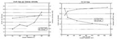
- FIG. 3shows a relationship between the susceptor temperature in the deposition process described above and the growth rate/thickness uniformity of the deposited film.
- Depositionswere conducted to form zirconium oxide (ZrO 2 ) thin films on 300-mm wafers in a PEALD reactor according to the deposition process described above.
- the depositionswere conducted while varying the susceptor temperature.
- a symbol “ ⁇ ”(sigma) represents standard deviation with respect to the thickness of a deposited film. Decreasing the susceptor temperature was not found to significantly adversely affect the growth rate of the film and the growth rate decreased when the temperature was decreased from 250° C. to 150° C.
- the thickness uniformity of the filmwas enhanced as the temperature was decreased.
- the resulting zirconium oxide filmswere found to have a k value of 35 or higher.
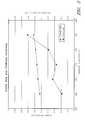
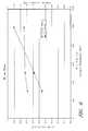
- FIGS. 4-7show relationships between the durations of the steps (1) to (4) of the deposition process described above and the growth rate/thickness uniformity of the deposited film.
- Depositionswere conducted to form zirconium oxide (ZrO 2 ) thin films on 300-mm wafers in a PEALD reactor according to the deposition process described above.
- the depositionswere conducted at a reactor temperature of 110° C. and a substrate temperature of about 250° C. 120 sccm of oxygen gas was continuously supplied to the reactor.
- a symbol “ ⁇ ”(sigma) represents standard deviation with respect to the thickness of a deposited film.
- Decreasing the supply duration D 1 ( FIG. 2 ) of a zirconium precursorwas not found to significantly adversely affect the growth rate and thickness uniformity of the film (see FIG. 4 ).
- decreasing the duration D 2 ( FIG. 2 ) of purging the zirconium precursordid not adversely affect the growth rate and thickness uniformity of the film (see FIG. 5 ).
- the duration D 2 of the purgewas decreased to 0, the growth rate increased.
- a zirconium oxide (ZrO 2 ) filmwas deposited on a 300 mm silicon wafer in a PEALD reactor having a showerhead (ASM Polygon 8300 Cluster tool in EmerALD® dielectric module) available from ASM America, Inc. (Phoenix, Ariz.). The wafer was placed on a susceptor within the reactor.
- ASM Polygon 8300 Cluster tool in EmerALD® dielectric moduleavailable from ASM America, Inc. (Phoenix, Ariz.).
- Example 1-6the temperature of the reactor was maintained at 100° C. to 350° C. during deposition.
- the temperature of a supply line from a gas source to the reactorwas maintained at 120° C.
- the temperature of the showerheadwas maintained at 130° C.
- Pressure in the reactor during depositionwas maintained at 6 torr.
- ZrD-04Bis(methylcyclopentadienyl)methylmethoxy zirconium (IV) available from Epichem Limited (Wirral, Great Britain) was supplied as a metal precursor into the reactor.
- the depositionwas conducted repeating a cycle which includes four steps of: (1) supplying the metal precursor into the reactor for 1.5 seconds; (2) purging for 4 seconds; (3) applying RF power to the reactor for 300 milliseconds; and (4) purging for 2 seconds. During the step (3), 75 W of RF power was applied to the reactor to generate in-situ oxygen plasma. Steps (1)-(4) were repeated until a zirconium oxide film having a thickness of about 100 ⁇ was formed on the wafer.
- Example 1the temperature of the susceptor was maintained at 150° C. In Example 2, the temperature of the susceptor was maintained at 250° C. In Example 3, the temperature of the susceptor was maintained at 350° C.
- Table 1The atomic concentrations of the zirconium oxide films resulting from Examples 1-3 are shown in Table 1 below. In Table 1, “HT” stands for a high-throughput process with shortened purge steps.
- Example 1(150° C.; 75 W) 32 60 3 5
- Example 2(250° C.; 75 W) 32 64 1 2.6
- Example 3(350° C.; 75 W) 37 61 ⁇ 1 2
- Example 4(100° C.; 200 W) 28 61 2 9
- Example 5(150° C.; 75 W; HT) 30 60 2 7
- Example 6(150° C.; 200 W: HT) 33 61 ⁇ 1 5
- the crystal structure resulting from Example 1was mainly amorphous with some crystallinity.
- the crystal structure resulting from Example 2was cubic and tetragonal.
- the crystal structure resulting from Example 3included a mixture of monoclinic/tetragonal phase.
- Example 4deposition was conducted under the same conditions as in Examples 1-3 except that 200 W of RF power was applied to the reactor during the step (3) and the temperature of the susceptor was maintained at 100° C.
- the atomic concentrations of the zirconium oxide film resulting from Example 4are shown in Table 1 above.
- depositionwas conducted with shortened purge steps.
- the depositionwas conducted repeating a cycle which includes four steps of: (1) supplying the metal precursor into the reactor for 300 milliseconds; (2) purging for 50 milliseconds; (3) applying RF power to the reactor for 300 milliseconds; and (4) purging for 50 milliseconds.
- the cyclewas repeated until a zirconium oxide film of thickness of about 100 ⁇ was formed on the wafer.
- Example 5the temperature of the susceptor was maintained at 150° C. During the step (3) of Example 5, 75 W of RF power was applied to the reactor to generate in-situ oxygen plasma.
- Example 6the temperature of the susceptor was maintained at 150° C. During the step (3) of Example 6, 200 W of RF power was applied to the reactor to generate in-situ oxygen plasma.
- the atomic concentrations of the zirconium oxide films resulting from Examples 5 and 6are shown in Table 1 above.
- the growth rate of Example 5was about 39 ⁇ /minute.
- the growth rate of Example 6was about 39 ⁇ /minute.
- the embodiments of the deposition process described abovemay be used for forming metal oxide films that can be part of various electronic devices.
- the electronic deviceinclude, but are not limited to, consumer electronic products, electronic circuits, electronic circuit components, parts of the consumer electronic products, electronic test equipments, etc.
- the consumer electronic productsmay include, but are not limited to, a mobile phone, a telephone, a television, a computer monitor, a computer, a hand-held computer, a personal digital assistant (PDA), a microwave, a refrigerator, a stereo system, a cassette recorder or player, a DVD player, a CD player, a VCR, an MP3 player, a radio, a camcorder, a camera, a digital camera, a portable memory chip, a washer, a dryer, a washer/dryer, a copier, a facsimile machine, a scanner, a multi functional peripheral device, a wrist watch, a clock, etc.
- the electronic devicemay include unfinished or partially fabricated products.
- the low-temperature process described abovedoes not adversely affect a thermally unstable material which has been already formed in a partially fabricated device during deposition of a metal oxide film on the device.
- materials chemically and/or physically unstable at temperatures of 200° C. or 250° C. or aboveare not adversely affected.
- the processcan be conducted with relatively short or substantially no purge steps while having substantially no adverse effect on the growth rate of the films. Thus, the throughput of the process can be significantly improved.
- the resulting metal oxide filmshave similar thickness uniformity, index of refraction and/or crystal structure as films deposited by a higher temperature process.
- the processproduces fewer impurity particles than a higher temperature process alternating two or more precursors because the metal precursor does not react with oxygen gas and background water at the low temperature that the process uses.
- any element used in an embodimentcan interchangeably be used in another embodiment unless such a replacement is not feasible. It will be appreciated by those skilled in the art that various other omissions, additions and modifications may be made to the methods and structures described above without departing from the scope of the invention. All such modifications and changes are intended to fall within the scope of the invention, as defined by the appended claims.
Landscapes
- Chemical & Material Sciences (AREA)
- Engineering & Computer Science (AREA)
- Organic Chemistry (AREA)
- Metallurgy (AREA)
- Physics & Mathematics (AREA)
- General Chemical & Material Sciences (AREA)
- Chemical Kinetics & Catalysis (AREA)
- Materials Engineering (AREA)
- Mechanical Engineering (AREA)
- Condensed Matter Physics & Semiconductors (AREA)
- Electromagnetism (AREA)
- Plasma & Fusion (AREA)
- General Physics & Mathematics (AREA)
- Manufacturing & Machinery (AREA)
- Computer Hardware Design (AREA)
- Microelectronics & Electronic Packaging (AREA)
- Power Engineering (AREA)
- Inorganic Chemistry (AREA)
- Formation Of Insulating Films (AREA)
- Chemical Vapour Deposition (AREA)
Abstract
Description
(R1Cp)2MR2R3 Formula 1
(R1Cp)MR2R3R4 Formula 2
| TABLE 1 | |||||
| Zr | O | C | H | ||
| (atomic | (atomic | (atomic | (atomic | ||
| %) | %) | %) | %) | ||
| Example 1 (150° C.; 75 W) | 32 | 60 | 3 | 5 |
| Example 2 (250° C.; 75 W) | 32 | 64 | 1 | 2.6 |
| Example 3 (350° C.; 75 W) | 37 | 61 | <1 | 2 |
| Example 4 (100° C.; 200 W) | 28 | 61 | 2 | 9 |
| Example 5 (150° C.; 75 W; HT) | 30 | 60 | 2 | 7 |
| Example 6 (150° C.; 200 W: HT) | 33 | 61 | <1 | 5 |
Claims (26)
(R1Cp)2MR2R3 Formula 1
(R1Cp)MR2R3R4 Formula 2
Priority Applications (1)
| Application Number | Priority Date | Filing Date | Title |
|---|---|---|---|
| US12/109,859US8383525B2 (en) | 2008-04-25 | 2008-04-25 | Plasma-enhanced deposition process for forming a metal oxide thin film and related structures |
Applications Claiming Priority (1)
| Application Number | Priority Date | Filing Date | Title |
|---|---|---|---|
| US12/109,859US8383525B2 (en) | 2008-04-25 | 2008-04-25 | Plasma-enhanced deposition process for forming a metal oxide thin film and related structures |
Publications (2)
| Publication Number | Publication Date |
|---|---|
| US20090269941A1 US20090269941A1 (en) | 2009-10-29 |
| US8383525B2true US8383525B2 (en) | 2013-02-26 |
Family
ID=41215433
Family Applications (1)
| Application Number | Title | Priority Date | Filing Date |
|---|---|---|---|
| US12/109,859Active2029-05-09US8383525B2 (en) | 2008-04-25 | 2008-04-25 | Plasma-enhanced deposition process for forming a metal oxide thin film and related structures |
Country Status (1)
| Country | Link |
|---|---|
| US (1) | US8383525B2 (en) |
Cited By (45)
| Publication number | Priority date | Publication date | Assignee | Title |
|---|---|---|---|---|
| US8956983B2 (en) | 2010-04-15 | 2015-02-17 | Novellus Systems, Inc. | Conformal doping via plasma activated atomic layer deposition and conformal film deposition |
| US8999859B2 (en) | 2010-04-15 | 2015-04-07 | Novellus Systems, Inc. | Plasma activated conformal dielectric film deposition |
| US9070555B2 (en)* | 2012-01-20 | 2015-06-30 | Novellus Systems, Inc. | Method for depositing a chlorine-free conformal sin film |
| US9076646B2 (en) | 2010-04-15 | 2015-07-07 | Lam Research Corporation | Plasma enhanced atomic layer deposition with pulsed plasma exposure |
| US9214334B2 (en) | 2014-02-18 | 2015-12-15 | Lam Research Corporation | High growth rate process for conformal aluminum nitride |
| US9214333B1 (en) | 2014-09-24 | 2015-12-15 | Lam Research Corporation | Methods and apparatuses for uniform reduction of the in-feature wet etch rate of a silicon nitride film formed by ALD |
| US9230800B2 (en) | 2010-04-15 | 2016-01-05 | Novellus Systems, Inc. | Plasma activated conformal film deposition |
| US9257274B2 (en) | 2010-04-15 | 2016-02-09 | Lam Research Corporation | Gapfill of variable aspect ratio features with a composite PEALD and PECVD method |
| US9287113B2 (en) | 2012-11-08 | 2016-03-15 | Novellus Systems, Inc. | Methods for depositing films on sensitive substrates |
| US20160138182A1 (en)* | 2014-11-18 | 2016-05-19 | Wisconsin Alumni Research Foundation | Methods for forming mixed metal oxide epitaxial films |
| US9355839B2 (en) | 2012-10-23 | 2016-05-31 | Lam Research Corporation | Sub-saturated atomic layer deposition and conformal film deposition |
| US9355886B2 (en) | 2010-04-15 | 2016-05-31 | Novellus Systems, Inc. | Conformal film deposition for gapfill |
| US9373500B2 (en) | 2014-02-21 | 2016-06-21 | Lam Research Corporation | Plasma assisted atomic layer deposition titanium oxide for conformal encapsulation and gapfill applications |
| US9390909B2 (en) | 2013-11-07 | 2016-07-12 | Novellus Systems, Inc. | Soft landing nanolaminates for advanced patterning |
| US9478411B2 (en) | 2014-08-20 | 2016-10-25 | Lam Research Corporation | Method to tune TiOx stoichiometry using atomic layer deposited Ti film to minimize contact resistance for TiOx/Ti based MIS contact scheme for CMOS |
| US9478438B2 (en) | 2014-08-20 | 2016-10-25 | Lam Research Corporation | Method and apparatus to deposit pure titanium thin film at low temperature using titanium tetraiodide precursor |
| US9502238B2 (en) | 2015-04-03 | 2016-11-22 | Lam Research Corporation | Deposition of conformal films by atomic layer deposition and atomic layer etch |
| US9564312B2 (en) | 2014-11-24 | 2017-02-07 | Lam Research Corporation | Selective inhibition in atomic layer deposition of silicon-containing films |
| US9589790B2 (en) | 2014-11-24 | 2017-03-07 | Lam Research Corporation | Method of depositing ammonia free and chlorine free conformal silicon nitride film |
| US9601693B1 (en) | 2015-09-24 | 2017-03-21 | Lam Research Corporation | Method for encapsulating a chalcogenide material |
| US9611544B2 (en) | 2010-04-15 | 2017-04-04 | Novellus Systems, Inc. | Plasma activated conformal dielectric film deposition |
| US9685320B2 (en) | 2010-09-23 | 2017-06-20 | Lam Research Corporation | Methods for depositing silicon oxide |
| US9773643B1 (en) | 2016-06-30 | 2017-09-26 | Lam Research Corporation | Apparatus and method for deposition and etch in gap fill |
| US9865455B1 (en) | 2016-09-07 | 2018-01-09 | Lam Research Corporation | Nitride film formed by plasma-enhanced and thermal atomic layer deposition process |
| US9892917B2 (en) | 2010-04-15 | 2018-02-13 | Lam Research Corporation | Plasma assisted atomic layer deposition of multi-layer films for patterning applications |
| US9997357B2 (en) | 2010-04-15 | 2018-06-12 | Lam Research Corporation | Capped ALD films for doping fin-shaped channel regions of 3-D IC transistors |
| US10037884B2 (en) | 2016-08-31 | 2018-07-31 | Lam Research Corporation | Selective atomic layer deposition for gapfill using sacrificial underlayer |
| US10062563B2 (en) | 2016-07-01 | 2018-08-28 | Lam Research Corporation | Selective atomic layer deposition with post-dose treatment |
| US10074543B2 (en) | 2016-08-31 | 2018-09-11 | Lam Research Corporation | High dry etch rate materials for semiconductor patterning applications |
| US10134579B2 (en) | 2016-11-14 | 2018-11-20 | Lam Research Corporation | Method for high modulus ALD SiO2 spacer |
| US10269559B2 (en) | 2017-09-13 | 2019-04-23 | Lam Research Corporation | Dielectric gapfill of high aspect ratio features utilizing a sacrificial etch cap layer |
| US10454029B2 (en) | 2016-11-11 | 2019-10-22 | Lam Research Corporation | Method for reducing the wet etch rate of a sin film without damaging the underlying substrate |
| US10526701B2 (en) | 2015-07-09 | 2020-01-07 | Lam Research Corporation | Multi-cycle ALD process for film uniformity and thickness profile modulation |
| US10629435B2 (en) | 2016-07-29 | 2020-04-21 | Lam Research Corporation | Doped ALD films for semiconductor patterning applications |
| US10832908B2 (en) | 2016-11-11 | 2020-11-10 | Lam Research Corporation | Self-aligned multi-patterning process flow with ALD gapfill spacer mask |
| US11404275B2 (en) | 2018-03-02 | 2022-08-02 | Lam Research Corporation | Selective deposition using hydrolysis |
| US11646198B2 (en) | 2015-03-20 | 2023-05-09 | Lam Research Corporation | Ultrathin atomic layer deposition film accuracy thickness control |
| US20230243036A1 (en)* | 2021-01-26 | 2023-08-03 | Asm Ip Holding B.V. | Methods and systems for depositing a layer |
| US20230290525A1 (en)* | 2022-03-14 | 2023-09-14 | The Trustees Of Princeton University | Planar coil stellarator |
| US12040181B2 (en) | 2019-05-01 | 2024-07-16 | Lam Research Corporation | Modulated atomic layer deposition |
| US12157945B2 (en) | 2019-08-06 | 2024-12-03 | Lam Research Corporation | Thermal atomic layer deposition of silicon-containing films |
| US12237175B2 (en) | 2019-06-04 | 2025-02-25 | Lam Research Corporation | Polymerization protective liner for reactive ion etch in patterning |
| US20250157677A1 (en)* | 2023-04-26 | 2025-05-15 | Thea Energy, Inc. | Planar coil stellarator including removable field shaping units |
| US12412742B2 (en) | 2020-07-28 | 2025-09-09 | Lam Research Corporation | Impurity reduction in silicon-containing films |
| US12431349B2 (en) | 2019-06-07 | 2025-09-30 | Lam Research Corporation | In-situ control of film properties during atomic layer deposition |
Families Citing this family (387)
| Publication number | Priority date | Publication date | Assignee | Title |
|---|---|---|---|---|
| FI117979B (en) | 2000-04-14 | 2007-05-15 | Asm Int | Process for making oxide thin films |
| US10378106B2 (en) | 2008-11-14 | 2019-08-13 | Asm Ip Holding B.V. | Method of forming insulation film by modified PEALD |
| US9394608B2 (en) | 2009-04-06 | 2016-07-19 | Asm America, Inc. | Semiconductor processing reactor and components thereof |
| US8802201B2 (en) | 2009-08-14 | 2014-08-12 | Asm America, Inc. | Systems and methods for thin-film deposition of metal oxides using excited nitrogen-oxygen species |
| JP5963456B2 (en) | 2011-02-18 | 2016-08-03 | 株式会社日立国際電気 | Semiconductor device manufacturing method, substrate processing apparatus, and substrate processing method |
| US9312155B2 (en) | 2011-06-06 | 2016-04-12 | Asm Japan K.K. | High-throughput semiconductor-processing apparatus equipped with multiple dual-chamber modules |
| US10364496B2 (en) | 2011-06-27 | 2019-07-30 | Asm Ip Holding B.V. | Dual section module having shared and unshared mass flow controllers |
| US10854498B2 (en) | 2011-07-15 | 2020-12-01 | Asm Ip Holding B.V. | Wafer-supporting device and method for producing same |
| US20130023129A1 (en) | 2011-07-20 | 2013-01-24 | Asm America, Inc. | Pressure transmitter for a semiconductor processing environment |
| US8759234B2 (en) | 2011-10-17 | 2014-06-24 | Taiwan Semiconductor Manufacturing Company, Ltd. | Deposited material and method of formation |
| US9017481B1 (en) | 2011-10-28 | 2015-04-28 | Asm America, Inc. | Process feed management for semiconductor substrate processing |
| US9558931B2 (en) | 2012-07-27 | 2017-01-31 | Asm Ip Holding B.V. | System and method for gas-phase sulfur passivation of a semiconductor surface |
| US9659799B2 (en) | 2012-08-28 | 2017-05-23 | Asm Ip Holding B.V. | Systems and methods for dynamic semiconductor process scheduling |
| US9021985B2 (en) | 2012-09-12 | 2015-05-05 | Asm Ip Holdings B.V. | Process gas management for an inductively-coupled plasma deposition reactor |
| US10714315B2 (en) | 2012-10-12 | 2020-07-14 | Asm Ip Holdings B.V. | Semiconductor reaction chamber showerhead |
| US20160376700A1 (en) | 2013-02-01 | 2016-12-29 | Asm Ip Holding B.V. | System for treatment of deposition reactor |
| US9484191B2 (en) | 2013-03-08 | 2016-11-01 | Asm Ip Holding B.V. | Pulsed remote plasma method and system |
| US9589770B2 (en) | 2013-03-08 | 2017-03-07 | Asm Ip Holding B.V. | Method and systems for in-situ formation of intermediate reactive species |
| US9824881B2 (en) | 2013-03-14 | 2017-11-21 | Asm Ip Holding B.V. | Si precursors for deposition of SiN at low temperatures |
| US9564309B2 (en) | 2013-03-14 | 2017-02-07 | Asm Ip Holding B.V. | Si precursors for deposition of SiN at low temperatures |
| US8993054B2 (en) | 2013-07-12 | 2015-03-31 | Asm Ip Holding B.V. | Method and system to reduce outgassing in a reaction chamber |
| US9240412B2 (en) | 2013-09-27 | 2016-01-19 | Asm Ip Holding B.V. | Semiconductor structure and device and methods of forming same using selective epitaxial process |
| US9605343B2 (en) | 2013-11-13 | 2017-03-28 | Asm Ip Holding B.V. | Method for forming conformal carbon films, structures conformal carbon film, and system of forming same |
| KR101493424B1 (en) | 2014-01-09 | 2015-02-16 | 연세대학교 산학협력단 | Epitaxial growth of dy-doped hafnium oxide |
| US10683571B2 (en) | 2014-02-25 | 2020-06-16 | Asm Ip Holding B.V. | Gas supply manifold and method of supplying gases to chamber using same |
| US10167557B2 (en) | 2014-03-18 | 2019-01-01 | Asm Ip Holding B.V. | Gas distribution system, reactor including the system, and methods of using the same |
| US11015245B2 (en) | 2014-03-19 | 2021-05-25 | Asm Ip Holding B.V. | Gas-phase reactor and system having exhaust plenum and components thereof |
| US10858737B2 (en) | 2014-07-28 | 2020-12-08 | Asm Ip Holding B.V. | Showerhead assembly and components thereof |
| US9890456B2 (en) | 2014-08-21 | 2018-02-13 | Asm Ip Holding B.V. | Method and system for in situ formation of gas-phase compounds |
| US20160056032A1 (en)* | 2014-08-22 | 2016-02-25 | Lam Research Corporation | Methods and apparatuses for stable deposition rate control in low temperature ald systems by showerhead active heating and/or pedestal cooling |
| US9576792B2 (en) | 2014-09-17 | 2017-02-21 | Asm Ip Holding B.V. | Deposition of SiN |
| US10941490B2 (en) | 2014-10-07 | 2021-03-09 | Asm Ip Holding B.V. | Multiple temperature range susceptor, assembly, reactor and system including the susceptor, and methods of using the same |
| US9657845B2 (en) | 2014-10-07 | 2017-05-23 | Asm Ip Holding B.V. | Variable conductance gas distribution apparatus and method |
| US10204764B2 (en) | 2014-10-28 | 2019-02-12 | Applied Materials, Inc. | Methods for forming a metal silicide interconnection nanowire structure |
| KR102300403B1 (en) | 2014-11-19 | 2021-09-09 | 에이에스엠 아이피 홀딩 비.브이. | Method of depositing thin film |
| US20160168699A1 (en)* | 2014-12-12 | 2016-06-16 | Asm Ip Holding B.V. | Method for depositing metal-containing film using particle-reduction step |
| KR102263121B1 (en) | 2014-12-22 | 2021-06-09 | 에이에스엠 아이피 홀딩 비.브이. | Semiconductor device and manufacuring method thereof |
| US10529542B2 (en) | 2015-03-11 | 2020-01-07 | Asm Ip Holdings B.V. | Cross-flow reactor and method |
| US10276355B2 (en) | 2015-03-12 | 2019-04-30 | Asm Ip Holding B.V. | Multi-zone reactor, system including the reactor, and method of using the same |
| US10458018B2 (en) | 2015-06-26 | 2019-10-29 | Asm Ip Holding B.V. | Structures including metal carbide material, devices including the structures, and methods of forming same |
| US10600673B2 (en) | 2015-07-07 | 2020-03-24 | Asm Ip Holding B.V. | Magnetic susceptor to baseplate seal |
| US10043661B2 (en) | 2015-07-13 | 2018-08-07 | Asm Ip Holding B.V. | Method for protecting layer by forming hydrocarbon-based extremely thin film |
| US10083836B2 (en) | 2015-07-24 | 2018-09-25 | Asm Ip Holding B.V. | Formation of boron-doped titanium metal films with high work function |
| US10087525B2 (en) | 2015-08-04 | 2018-10-02 | Asm Ip Holding B.V. | Variable gap hard stop design |
| US9647114B2 (en) | 2015-08-14 | 2017-05-09 | Asm Ip Holding B.V. | Methods of forming highly p-type doped germanium tin films and structures and devices including the films |
| US10410857B2 (en) | 2015-08-24 | 2019-09-10 | Asm Ip Holding B.V. | Formation of SiN thin films |
| US9960072B2 (en) | 2015-09-29 | 2018-05-01 | Asm Ip Holding B.V. | Variable adjustment for precise matching of multiple chamber cavity housings |
| US10211308B2 (en) | 2015-10-21 | 2019-02-19 | Asm Ip Holding B.V. | NbMC layers |
| US10322384B2 (en) | 2015-11-09 | 2019-06-18 | Asm Ip Holding B.V. | Counter flow mixer for process chamber |
| US9627221B1 (en) | 2015-12-28 | 2017-04-18 | Asm Ip Holding B.V. | Continuous process incorporating atomic layer etching |
| US11139308B2 (en) | 2015-12-29 | 2021-10-05 | Asm Ip Holding B.V. | Atomic layer deposition of III-V compounds to form V-NAND devices |
| US10468251B2 (en) | 2016-02-19 | 2019-11-05 | Asm Ip Holding B.V. | Method for forming spacers using silicon nitride film for spacer-defined multiple patterning |
| US10529554B2 (en) | 2016-02-19 | 2020-01-07 | Asm Ip Holding B.V. | Method for forming silicon nitride film selectively on sidewalls or flat surfaces of trenches |
| US10501866B2 (en) | 2016-03-09 | 2019-12-10 | Asm Ip Holding B.V. | Gas distribution apparatus for improved film uniformity in an epitaxial system |
| US10343920B2 (en) | 2016-03-18 | 2019-07-09 | Asm Ip Holding B.V. | Aligned carbon nanotubes |
| US9892913B2 (en) | 2016-03-24 | 2018-02-13 | Asm Ip Holding B.V. | Radial and thickness control via biased multi-port injection settings |
| US10865475B2 (en) | 2016-04-21 | 2020-12-15 | Asm Ip Holding B.V. | Deposition of metal borides and silicides |
| US10190213B2 (en) | 2016-04-21 | 2019-01-29 | Asm Ip Holding B.V. | Deposition of metal borides |
| US10087522B2 (en) | 2016-04-21 | 2018-10-02 | Asm Ip Holding B.V. | Deposition of metal borides |
| US10032628B2 (en) | 2016-05-02 | 2018-07-24 | Asm Ip Holding B.V. | Source/drain performance through conformal solid state doping |
| US10367080B2 (en) | 2016-05-02 | 2019-07-30 | Asm Ip Holding B.V. | Method of forming a germanium oxynitride film |
| KR102592471B1 (en) | 2016-05-17 | 2023-10-20 | 에이에스엠 아이피 홀딩 비.브이. | Method of forming metal interconnection and method of fabricating semiconductor device using the same |
| US11453943B2 (en) | 2016-05-25 | 2022-09-27 | Asm Ip Holding B.V. | Method for forming carbon-containing silicon/metal oxide or nitride film by ALD using silicon precursor and hydrocarbon precursor |
| US10388509B2 (en) | 2016-06-28 | 2019-08-20 | Asm Ip Holding B.V. | Formation of epitaxial layers via dislocation filtering |
| US9859151B1 (en) | 2016-07-08 | 2018-01-02 | Asm Ip Holding B.V. | Selective film deposition method to form air gaps |
| US10612137B2 (en) | 2016-07-08 | 2020-04-07 | Asm Ip Holdings B.V. | Organic reactants for atomic layer deposition |
| US9793135B1 (en) | 2016-07-14 | 2017-10-17 | ASM IP Holding B.V | Method of cyclic dry etching using etchant film |
| US10714385B2 (en) | 2016-07-19 | 2020-07-14 | Asm Ip Holding B.V. | Selective deposition of tungsten |
| KR102354490B1 (en) | 2016-07-27 | 2022-01-21 | 에이에스엠 아이피 홀딩 비.브이. | Method of processing a substrate |
| US9887082B1 (en) | 2016-07-28 | 2018-02-06 | Asm Ip Holding B.V. | Method and apparatus for filling a gap |
| US10177025B2 (en) | 2016-07-28 | 2019-01-08 | Asm Ip Holding B.V. | Method and apparatus for filling a gap |
| US9812320B1 (en) | 2016-07-28 | 2017-11-07 | Asm Ip Holding B.V. | Method and apparatus for filling a gap |
| KR102532607B1 (en) | 2016-07-28 | 2023-05-15 | 에이에스엠 아이피 홀딩 비.브이. | Substrate processing apparatus and method of operating the same |
| US10395919B2 (en) | 2016-07-28 | 2019-08-27 | Asm Ip Holding B.V. | Method and apparatus for filling a gap |
| US10347547B2 (en) | 2016-08-09 | 2019-07-09 | Lam Research Corporation | Suppressing interfacial reactions by varying the wafer temperature throughout deposition |
| US10090316B2 (en) | 2016-09-01 | 2018-10-02 | Asm Ip Holding B.V. | 3D stacked multilayer semiconductor memory using doped select transistor channel |
| US10410943B2 (en) | 2016-10-13 | 2019-09-10 | Asm Ip Holding B.V. | Method for passivating a surface of a semiconductor and related systems |
| US10643826B2 (en) | 2016-10-26 | 2020-05-05 | Asm Ip Holdings B.V. | Methods for thermally calibrating reaction chambers |
| US11532757B2 (en) | 2016-10-27 | 2022-12-20 | Asm Ip Holding B.V. | Deposition of charge trapping layers |
| US10714350B2 (en) | 2016-11-01 | 2020-07-14 | ASM IP Holdings, B.V. | Methods for forming a transition metal niobium nitride film on a substrate by atomic layer deposition and related semiconductor device structures |
| US10229833B2 (en) | 2016-11-01 | 2019-03-12 | Asm Ip Holding B.V. | Methods for forming a transition metal nitride film on a substrate by atomic layer deposition and related semiconductor device structures |
| US10643904B2 (en) | 2016-11-01 | 2020-05-05 | Asm Ip Holdings B.V. | Methods for forming a semiconductor device and related semiconductor device structures |
| US10435790B2 (en) | 2016-11-01 | 2019-10-08 | Asm Ip Holding B.V. | Method of subatmospheric plasma-enhanced ALD using capacitively coupled electrodes with narrow gap |
| US10134757B2 (en) | 2016-11-07 | 2018-11-20 | Asm Ip Holding B.V. | Method of processing a substrate and a device manufactured by using the method |
| KR102546317B1 (en) | 2016-11-15 | 2023-06-21 | 에이에스엠 아이피 홀딩 비.브이. | Gas supply unit and substrate processing apparatus including the same |
| US10340135B2 (en) | 2016-11-28 | 2019-07-02 | Asm Ip Holding B.V. | Method of topologically restricted plasma-enhanced cyclic deposition of silicon or metal nitride |
| KR102762543B1 (en) | 2016-12-14 | 2025-02-05 | 에이에스엠 아이피 홀딩 비.브이. | Substrate processing apparatus |
| US11581186B2 (en) | 2016-12-15 | 2023-02-14 | Asm Ip Holding B.V. | Sequential infiltration synthesis apparatus |
| US9916980B1 (en) | 2016-12-15 | 2018-03-13 | Asm Ip Holding B.V. | Method of forming a structure on a substrate |
| US11447861B2 (en) | 2016-12-15 | 2022-09-20 | Asm Ip Holding B.V. | Sequential infiltration synthesis apparatus and a method of forming a patterned structure |
| KR102700194B1 (en) | 2016-12-19 | 2024-08-28 | 에이에스엠 아이피 홀딩 비.브이. | Substrate processing apparatus |
| US10269558B2 (en) | 2016-12-22 | 2019-04-23 | Asm Ip Holding B.V. | Method of forming a structure on a substrate |
| US10867788B2 (en) | 2016-12-28 | 2020-12-15 | Asm Ip Holding B.V. | Method of forming a structure on a substrate |
| US11390950B2 (en) | 2017-01-10 | 2022-07-19 | Asm Ip Holding B.V. | Reactor system and method to reduce residue buildup during a film deposition process |
| KR20210146421A (en)* | 2017-01-16 | 2021-12-03 | 엔테그리스, 아이엔씨. | Articles coated with a fluoro-annealed film |
| US10655221B2 (en) | 2017-02-09 | 2020-05-19 | Asm Ip Holding B.V. | Method for depositing oxide film by thermal ALD and PEALD |
| US10468261B2 (en) | 2017-02-15 | 2019-11-05 | Asm Ip Holding B.V. | Methods for forming a metallic film on a substrate by cyclical deposition and related semiconductor device structures |
| US10283353B2 (en) | 2017-03-29 | 2019-05-07 | Asm Ip Holding B.V. | Method of reforming insulating film deposited on substrate with recess pattern |
| US10529563B2 (en) | 2017-03-29 | 2020-01-07 | Asm Ip Holdings B.V. | Method for forming doped metal oxide films on a substrate by cyclical deposition and related semiconductor device structures |
| US10103040B1 (en) | 2017-03-31 | 2018-10-16 | Asm Ip Holding B.V. | Apparatus and method for manufacturing a semiconductor device |
| USD830981S1 (en) | 2017-04-07 | 2018-10-16 | Asm Ip Holding B.V. | Susceptor for semiconductor substrate processing apparatus |
| KR102457289B1 (en) | 2017-04-25 | 2022-10-21 | 에이에스엠 아이피 홀딩 비.브이. | Method for depositing a thin film and manufacturing a semiconductor device |
| US10770286B2 (en) | 2017-05-08 | 2020-09-08 | Asm Ip Holdings B.V. | Methods for selectively forming a silicon nitride film on a substrate and related semiconductor device structures |
| US10892156B2 (en) | 2017-05-08 | 2021-01-12 | Asm Ip Holding B.V. | Methods for forming a silicon nitride film on a substrate and related semiconductor device structures |
| US10446393B2 (en) | 2017-05-08 | 2019-10-15 | Asm Ip Holding B.V. | Methods for forming silicon-containing epitaxial layers and related semiconductor device structures |
| US10504742B2 (en) | 2017-05-31 | 2019-12-10 | Asm Ip Holding B.V. | Method of atomic layer etching using hydrogen plasma |
| US10886123B2 (en) | 2017-06-02 | 2021-01-05 | Asm Ip Holding B.V. | Methods for forming low temperature semiconductor layers and related semiconductor device structures |
| US12040200B2 (en) | 2017-06-20 | 2024-07-16 | Asm Ip Holding B.V. | Semiconductor processing apparatus and methods for calibrating a semiconductor processing apparatus |
| US11306395B2 (en) | 2017-06-28 | 2022-04-19 | Asm Ip Holding B.V. | Methods for depositing a transition metal nitride film on a substrate by atomic layer deposition and related deposition apparatus |
| US10685834B2 (en) | 2017-07-05 | 2020-06-16 | Asm Ip Holdings B.V. | Methods for forming a silicon germanium tin layer and related semiconductor device structures |
| KR20190009245A (en) | 2017-07-18 | 2019-01-28 | 에이에스엠 아이피 홀딩 비.브이. | Methods for forming a semiconductor device structure and related semiconductor device structures |
| US11018002B2 (en) | 2017-07-19 | 2021-05-25 | Asm Ip Holding B.V. | Method for selectively depositing a Group IV semiconductor and related semiconductor device structures |
| US10541333B2 (en) | 2017-07-19 | 2020-01-21 | Asm Ip Holding B.V. | Method for depositing a group IV semiconductor and related semiconductor device structures |
| US11374112B2 (en) | 2017-07-19 | 2022-06-28 | Asm Ip Holding B.V. | Method for depositing a group IV semiconductor and related semiconductor device structures |
| US10605530B2 (en) | 2017-07-26 | 2020-03-31 | Asm Ip Holding B.V. | Assembly of a liner and a flange for a vertical furnace as well as the liner and the vertical furnace |
| US10590535B2 (en) | 2017-07-26 | 2020-03-17 | Asm Ip Holdings B.V. | Chemical treatment, deposition and/or infiltration apparatus and method for using the same |
| US10312055B2 (en) | 2017-07-26 | 2019-06-04 | Asm Ip Holding B.V. | Method of depositing film by PEALD using negative bias |
| TWI815813B (en) | 2017-08-04 | 2023-09-21 | 荷蘭商Asm智慧財產控股公司 | Showerhead assembly for distributing a gas within a reaction chamber |
| US10770336B2 (en) | 2017-08-08 | 2020-09-08 | Asm Ip Holding B.V. | Substrate lift mechanism and reactor including same |
| US10692741B2 (en) | 2017-08-08 | 2020-06-23 | Asm Ip Holdings B.V. | Radiation shield |
| US10249524B2 (en) | 2017-08-09 | 2019-04-02 | Asm Ip Holding B.V. | Cassette holder assembly for a substrate cassette and holding member for use in such assembly |
| US11139191B2 (en) | 2017-08-09 | 2021-10-05 | Asm Ip Holding B.V. | Storage apparatus for storing cassettes for substrates and processing apparatus equipped therewith |
| US11769682B2 (en) | 2017-08-09 | 2023-09-26 | Asm Ip Holding B.V. | Storage apparatus for storing cassettes for substrates and processing apparatus equipped therewith |
| US10236177B1 (en) | 2017-08-22 | 2019-03-19 | ASM IP Holding B.V.. | Methods for depositing a doped germanium tin semiconductor and related semiconductor device structures |
| USD900036S1 (en) | 2017-08-24 | 2020-10-27 | Asm Ip Holding B.V. | Heater electrical connector and adapter |
| US11830730B2 (en) | 2017-08-29 | 2023-11-28 | Asm Ip Holding B.V. | Layer forming method and apparatus |
| US11295980B2 (en) | 2017-08-30 | 2022-04-05 | Asm Ip Holding B.V. | Methods for depositing a molybdenum metal film over a dielectric surface of a substrate by a cyclical deposition process and related semiconductor device structures |
| US11056344B2 (en) | 2017-08-30 | 2021-07-06 | Asm Ip Holding B.V. | Layer forming method |
| KR102491945B1 (en) | 2017-08-30 | 2023-01-26 | 에이에스엠 아이피 홀딩 비.브이. | Substrate processing apparatus |
| KR102401446B1 (en) | 2017-08-31 | 2022-05-24 | 에이에스엠 아이피 홀딩 비.브이. | Substrate processing apparatus |
| US10607895B2 (en) | 2017-09-18 | 2020-03-31 | Asm Ip Holdings B.V. | Method for forming a semiconductor device structure comprising a gate fill metal |
| KR102630301B1 (en) | 2017-09-21 | 2024-01-29 | 에이에스엠 아이피 홀딩 비.브이. | Method of sequential infiltration synthesis treatment of infiltrateable material and structures and devices formed using same |
| US10844484B2 (en) | 2017-09-22 | 2020-11-24 | Asm Ip Holding B.V. | Apparatus for dispensing a vapor phase reactant to a reaction chamber and related methods |
| US10658205B2 (en) | 2017-09-28 | 2020-05-19 | Asm Ip Holdings B.V. | Chemical dispensing apparatus and methods for dispensing a chemical to a reaction chamber |
| US10403504B2 (en) | 2017-10-05 | 2019-09-03 | Asm Ip Holding B.V. | Method for selectively depositing a metallic film on a substrate |
| US10319588B2 (en) | 2017-10-10 | 2019-06-11 | Asm Ip Holding B.V. | Method for depositing a metal chalcogenide on a substrate by cyclical deposition |
| KR102470206B1 (en)* | 2017-10-13 | 2022-11-23 | 삼성디스플레이 주식회사 | Manufacturing method for metal oxide and display device comprising the metal oxide |
| US10923344B2 (en) | 2017-10-30 | 2021-02-16 | Asm Ip Holding B.V. | Methods for forming a semiconductor structure and related semiconductor structures |
| KR102443047B1 (en) | 2017-11-16 | 2022-09-14 | 에이에스엠 아이피 홀딩 비.브이. | Method of processing a substrate and a device manufactured by the same |
| US10910262B2 (en) | 2017-11-16 | 2021-02-02 | Asm Ip Holding B.V. | Method of selectively depositing a capping layer structure on a semiconductor device structure |
| US11022879B2 (en) | 2017-11-24 | 2021-06-01 | Asm Ip Holding B.V. | Method of forming an enhanced unexposed photoresist layer |
| WO2019103613A1 (en) | 2017-11-27 | 2019-05-31 | Asm Ip Holding B.V. | A storage device for storing wafer cassettes for use with a batch furnace |
| CN111344522B (en) | 2017-11-27 | 2022-04-12 | 阿斯莫Ip控股公司 | Including clean mini-environment device |
| US10290508B1 (en) | 2017-12-05 | 2019-05-14 | Asm Ip Holding B.V. | Method for forming vertical spacers for spacer-defined patterning |
| US10872771B2 (en) | 2018-01-16 | 2020-12-22 | Asm Ip Holding B. V. | Method for depositing a material film on a substrate within a reaction chamber by a cyclical deposition process and related device structures |
| TWI799494B (en) | 2018-01-19 | 2023-04-21 | 荷蘭商Asm 智慧財產控股公司 | Deposition method |
| KR102695659B1 (en) | 2018-01-19 | 2024-08-14 | 에이에스엠 아이피 홀딩 비.브이. | Method for depositing a gap filling layer by plasma assisted deposition |
| USD903477S1 (en) | 2018-01-24 | 2020-12-01 | Asm Ip Holdings B.V. | Metal clamp |
| US11018047B2 (en) | 2018-01-25 | 2021-05-25 | Asm Ip Holding B.V. | Hybrid lift pin |
| US10535516B2 (en) | 2018-02-01 | 2020-01-14 | Asm Ip Holdings B.V. | Method for depositing a semiconductor structure on a surface of a substrate and related semiconductor structures |
| USD880437S1 (en) | 2018-02-01 | 2020-04-07 | Asm Ip Holding B.V. | Gas supply plate for semiconductor manufacturing apparatus |
| US11081345B2 (en) | 2018-02-06 | 2021-08-03 | Asm Ip Holding B.V. | Method of post-deposition treatment for silicon oxide film |
| WO2019158960A1 (en) | 2018-02-14 | 2019-08-22 | Asm Ip Holding B.V. | A method for depositing a ruthenium-containing film on a substrate by a cyclical deposition process |
| US10896820B2 (en) | 2018-02-14 | 2021-01-19 | Asm Ip Holding B.V. | Method for depositing a ruthenium-containing film on a substrate by a cyclical deposition process |
| US10731249B2 (en) | 2018-02-15 | 2020-08-04 | Asm Ip Holding B.V. | Method of forming a transition metal containing film on a substrate by a cyclical deposition process, a method for supplying a transition metal halide compound to a reaction chamber, and related vapor deposition apparatus |
| KR102636427B1 (en) | 2018-02-20 | 2024-02-13 | 에이에스엠 아이피 홀딩 비.브이. | Substrate processing method and apparatus |
| US10658181B2 (en) | 2018-02-20 | 2020-05-19 | Asm Ip Holding B.V. | Method of spacer-defined direct patterning in semiconductor fabrication |
| US10975470B2 (en) | 2018-02-23 | 2021-04-13 | Asm Ip Holding B.V. | Apparatus for detecting or monitoring for a chemical precursor in a high temperature environment |
| US11473195B2 (en) | 2018-03-01 | 2022-10-18 | Asm Ip Holding B.V. | Semiconductor processing apparatus and a method for processing a substrate |
| US11629406B2 (en) | 2018-03-09 | 2023-04-18 | Asm Ip Holding B.V. | Semiconductor processing apparatus comprising one or more pyrometers for measuring a temperature of a substrate during transfer of the substrate |
| US11114283B2 (en) | 2018-03-16 | 2021-09-07 | Asm Ip Holding B.V. | Reactor, system including the reactor, and methods of manufacturing and using same |
| KR102646467B1 (en) | 2018-03-27 | 2024-03-11 | 에이에스엠 아이피 홀딩 비.브이. | Method of forming an electrode on a substrate and a semiconductor device structure including an electrode |
| US10510536B2 (en) | 2018-03-29 | 2019-12-17 | Asm Ip Holding B.V. | Method of depositing a co-doped polysilicon film on a surface of a substrate within a reaction chamber |
| US11088002B2 (en) | 2018-03-29 | 2021-08-10 | Asm Ip Holding B.V. | Substrate rack and a substrate processing system and method |
| US11230766B2 (en) | 2018-03-29 | 2022-01-25 | Asm Ip Holding B.V. | Substrate processing apparatus and method |
| KR102501472B1 (en) | 2018-03-30 | 2023-02-20 | 에이에스엠 아이피 홀딩 비.브이. | Substrate processing method |
| KR102600229B1 (en) | 2018-04-09 | 2023-11-10 | 에이에스엠 아이피 홀딩 비.브이. | Substrate supporting device, substrate processing apparatus including the same and substrate processing method |
| US10580645B2 (en) | 2018-04-30 | 2020-03-03 | Asm Ip Holding B.V. | Plasma enhanced atomic layer deposition (PEALD) of SiN using silicon-hydrohalide precursors |
| US12025484B2 (en) | 2018-05-08 | 2024-07-02 | Asm Ip Holding B.V. | Thin film forming method |
| TWI811348B (en) | 2018-05-08 | 2023-08-11 | 荷蘭商Asm 智慧財產控股公司 | Methods for depositing an oxide film on a substrate by a cyclical deposition process and related device structures |
| US12272527B2 (en) | 2018-05-09 | 2025-04-08 | Asm Ip Holding B.V. | Apparatus for use with hydrogen radicals and method of using same |
| KR20190129718A (en) | 2018-05-11 | 2019-11-20 | 에이에스엠 아이피 홀딩 비.브이. | Methods for forming a doped metal carbide film on a substrate and related semiconductor device structures |
| KR102596988B1 (en) | 2018-05-28 | 2023-10-31 | 에이에스엠 아이피 홀딩 비.브이. | Method of processing a substrate and a device manufactured by the same |
| US11718913B2 (en) | 2018-06-04 | 2023-08-08 | Asm Ip Holding B.V. | Gas distribution system and reactor system including same |
| TWI840362B (en) | 2018-06-04 | 2024-05-01 | 荷蘭商Asm Ip私人控股有限公司 | Wafer handling chamber with moisture reduction |
| US11286562B2 (en) | 2018-06-08 | 2022-03-29 | Asm Ip Holding B.V. | Gas-phase chemical reactor and method of using same |
| KR102568797B1 (en) | 2018-06-21 | 2023-08-21 | 에이에스엠 아이피 홀딩 비.브이. | Substrate processing system |
| US10797133B2 (en) | 2018-06-21 | 2020-10-06 | Asm Ip Holding B.V. | Method for depositing a phosphorus doped silicon arsenide film and related semiconductor device structures |
| KR102854019B1 (en) | 2018-06-27 | 2025-09-02 | 에이에스엠 아이피 홀딩 비.브이. | Periodic deposition method for forming a metal-containing material and films and structures comprising the metal-containing material |
| TWI873894B (en) | 2018-06-27 | 2025-02-21 | 荷蘭商Asm Ip私人控股有限公司 | Cyclic deposition methods for forming metal-containing material and films and structures including the metal-containing material |
| US10612136B2 (en) | 2018-06-29 | 2020-04-07 | ASM IP Holding, B.V. | Temperature-controlled flange and reactor system including same |
| KR102686758B1 (en) | 2018-06-29 | 2024-07-18 | 에이에스엠 아이피 홀딩 비.브이. | Method for depositing a thin film and manufacturing a semiconductor device |
| US10388513B1 (en) | 2018-07-03 | 2019-08-20 | Asm Ip Holding B.V. | Method for depositing silicon-free carbon-containing film as gap-fill layer by pulse plasma-assisted deposition |
| US10755922B2 (en) | 2018-07-03 | 2020-08-25 | Asm Ip Holding B.V. | Method for depositing silicon-free carbon-containing film as gap-fill layer by pulse plasma-assisted deposition |
| US10767789B2 (en) | 2018-07-16 | 2020-09-08 | Asm Ip Holding B.V. | Diaphragm valves, valve components, and methods for forming valve components |
| US10483099B1 (en) | 2018-07-26 | 2019-11-19 | Asm Ip Holding B.V. | Method for forming thermally stable organosilicon polymer film |
| US11053591B2 (en) | 2018-08-06 | 2021-07-06 | Asm Ip Holding B.V. | Multi-port gas injection system and reactor system including same |
| US10883175B2 (en) | 2018-08-09 | 2021-01-05 | Asm Ip Holding B.V. | Vertical furnace for processing substrates and a liner for use therein |
| US10829852B2 (en) | 2018-08-16 | 2020-11-10 | Asm Ip Holding B.V. | Gas distribution device for a wafer processing apparatus |
| US11430674B2 (en) | 2018-08-22 | 2022-08-30 | Asm Ip Holding B.V. | Sensor array, apparatus for dispensing a vapor phase reactant to a reaction chamber and related methods |
| KR102707956B1 (en) | 2018-09-11 | 2024-09-19 | 에이에스엠 아이피 홀딩 비.브이. | Method for deposition of a thin film |
| US11024523B2 (en) | 2018-09-11 | 2021-06-01 | Asm Ip Holding B.V. | Substrate processing apparatus and method |
| US11049751B2 (en) | 2018-09-14 | 2021-06-29 | Asm Ip Holding B.V. | Cassette supply system to store and handle cassettes and processing apparatus equipped therewith |
| CN110970344B (en) | 2018-10-01 | 2024-10-25 | Asmip控股有限公司 | Substrate holding apparatus, system comprising the same and method of using the same |
| US11232963B2 (en) | 2018-10-03 | 2022-01-25 | Asm Ip Holding B.V. | Substrate processing apparatus and method |
| KR102592699B1 (en) | 2018-10-08 | 2023-10-23 | 에이에스엠 아이피 홀딩 비.브이. | Substrate support unit and apparatuses for depositing thin film and processing the substrate including the same |
| US10847365B2 (en) | 2018-10-11 | 2020-11-24 | Asm Ip Holding B.V. | Method of forming conformal silicon carbide film by cyclic CVD |
| US10811256B2 (en) | 2018-10-16 | 2020-10-20 | Asm Ip Holding B.V. | Method for etching a carbon-containing feature |
| KR102605121B1 (en) | 2018-10-19 | 2023-11-23 | 에이에스엠 아이피 홀딩 비.브이. | Substrate processing apparatus and substrate processing method |
| KR102546322B1 (en) | 2018-10-19 | 2023-06-21 | 에이에스엠 아이피 홀딩 비.브이. | Substrate processing apparatus and substrate processing method |
| USD948463S1 (en) | 2018-10-24 | 2022-04-12 | Asm Ip Holding B.V. | Susceptor for semiconductor substrate supporting apparatus |
| US10381219B1 (en) | 2018-10-25 | 2019-08-13 | Asm Ip Holding B.V. | Methods for forming a silicon nitride film |
| US12378665B2 (en) | 2018-10-26 | 2025-08-05 | Asm Ip Holding B.V. | High temperature coatings for a preclean and etch apparatus and related methods |
| US11087997B2 (en) | 2018-10-31 | 2021-08-10 | Asm Ip Holding B.V. | Substrate processing apparatus for processing substrates |
| KR102748291B1 (en) | 2018-11-02 | 2024-12-31 | 에이에스엠 아이피 홀딩 비.브이. | Substrate support unit and substrate processing apparatus including the same |
| CN111146320A (en)* | 2018-11-02 | 2020-05-12 | 华为技术有限公司 | Silicon-based substrate, substrate base plate and manufacturing method thereof, and photoelectric device |
| US11572620B2 (en) | 2018-11-06 | 2023-02-07 | Asm Ip Holding B.V. | Methods for selectively depositing an amorphous silicon film on a substrate |
| US11031242B2 (en) | 2018-11-07 | 2021-06-08 | Asm Ip Holding B.V. | Methods for depositing a boron doped silicon germanium film |
| US10847366B2 (en) | 2018-11-16 | 2020-11-24 | Asm Ip Holding B.V. | Methods for depositing a transition metal chalcogenide film on a substrate by a cyclical deposition process |
| US10818758B2 (en) | 2018-11-16 | 2020-10-27 | Asm Ip Holding B.V. | Methods for forming a metal silicate film on a substrate in a reaction chamber and related semiconductor device structures |
| US10559458B1 (en) | 2018-11-26 | 2020-02-11 | Asm Ip Holding B.V. | Method of forming oxynitride film |
| US12040199B2 (en) | 2018-11-28 | 2024-07-16 | Asm Ip Holding B.V. | Substrate processing apparatus for processing substrates |
| US11217444B2 (en) | 2018-11-30 | 2022-01-04 | Asm Ip Holding B.V. | Method for forming an ultraviolet radiation responsive metal oxide-containing film |
| KR102636428B1 (en) | 2018-12-04 | 2024-02-13 | 에이에스엠 아이피 홀딩 비.브이. | A method for cleaning a substrate processing apparatus |
| US11158513B2 (en) | 2018-12-13 | 2021-10-26 | Asm Ip Holding B.V. | Methods for forming a rhenium-containing film on a substrate by a cyclical deposition process and related semiconductor device structures |
| TWI874340B (en) | 2018-12-14 | 2025-03-01 | 荷蘭商Asm Ip私人控股有限公司 | Method of forming device structure, structure formed by the method and system for performing the method |
| TWI866480B (en) | 2019-01-17 | 2024-12-11 | 荷蘭商Asm Ip 私人控股有限公司 | Methods of forming a transition metal containing film on a substrate by a cyclical deposition process |
| KR102727227B1 (en) | 2019-01-22 | 2024-11-07 | 에이에스엠 아이피 홀딩 비.브이. | Semiconductor processing device |
| CN111524788B (en) | 2019-02-01 | 2023-11-24 | Asm Ip私人控股有限公司 | Method for forming topologically selective films of silicon oxide |
| TWI838458B (en) | 2019-02-20 | 2024-04-11 | 荷蘭商Asm Ip私人控股有限公司 | Apparatus and methods for plug fill deposition in 3-d nand applications |
| TWI845607B (en) | 2019-02-20 | 2024-06-21 | 荷蘭商Asm Ip私人控股有限公司 | Cyclical deposition method and apparatus for filling a recess formed within a substrate surface |
| KR102626263B1 (en) | 2019-02-20 | 2024-01-16 | 에이에스엠 아이피 홀딩 비.브이. | Cyclical deposition method including treatment step and apparatus for same |
| TWI873122B (en) | 2019-02-20 | 2025-02-21 | 荷蘭商Asm Ip私人控股有限公司 | Method of filling a recess formed within a surface of a substrate, semiconductor structure formed according to the method, and semiconductor processing apparatus |
| TWI842826B (en) | 2019-02-22 | 2024-05-21 | 荷蘭商Asm Ip私人控股有限公司 | Substrate processing apparatus and method for processing substrate |
| KR102782593B1 (en) | 2019-03-08 | 2025-03-14 | 에이에스엠 아이피 홀딩 비.브이. | Structure Including SiOC Layer and Method of Forming Same |
| US11742198B2 (en) | 2019-03-08 | 2023-08-29 | Asm Ip Holding B.V. | Structure including SiOCN layer and method of forming same |
| KR102858005B1 (en) | 2019-03-08 | 2025-09-09 | 에이에스엠 아이피 홀딩 비.브이. | Method for Selective Deposition of Silicon Nitride Layer and Structure Including Selectively-Deposited Silicon Nitride Layer |
| JP2020167398A (en) | 2019-03-28 | 2020-10-08 | エーエスエム・アイピー・ホールディング・ベー・フェー | Door openers and substrate processing equipment provided with door openers |
| KR102809999B1 (en) | 2019-04-01 | 2025-05-19 | 에이에스엠 아이피 홀딩 비.브이. | Method of manufacturing semiconductor device |
| KR20200123380A (en) | 2019-04-19 | 2020-10-29 | 에이에스엠 아이피 홀딩 비.브이. | Layer forming method and apparatus |
| KR20200125453A (en) | 2019-04-24 | 2020-11-04 | 에이에스엠 아이피 홀딩 비.브이. | Gas-phase reactor system and method of using same |
| KR20200130121A (en) | 2019-05-07 | 2020-11-18 | 에이에스엠 아이피 홀딩 비.브이. | Chemical source vessel with dip tube |
| US11289326B2 (en) | 2019-05-07 | 2022-03-29 | Asm Ip Holding B.V. | Method for reforming amorphous carbon polymer film |
| KR20200130652A (en) | 2019-05-10 | 2020-11-19 | 에이에스엠 아이피 홀딩 비.브이. | Method of depositing material onto a surface and structure formed according to the method |
| JP7598201B2 (en) | 2019-05-16 | 2024-12-11 | エーエスエム・アイピー・ホールディング・ベー・フェー | Wafer boat handling apparatus, vertical batch furnace and method |
| JP7612342B2 (en) | 2019-05-16 | 2025-01-14 | エーエスエム・アイピー・ホールディング・ベー・フェー | Wafer boat handling apparatus, vertical batch furnace and method |
| USD947913S1 (en) | 2019-05-17 | 2022-04-05 | Asm Ip Holding B.V. | Susceptor shaft |
| USD975665S1 (en) | 2019-05-17 | 2023-01-17 | Asm Ip Holding B.V. | Susceptor shaft |
| USD935572S1 (en) | 2019-05-24 | 2021-11-09 | Asm Ip Holding B.V. | Gas channel plate |
| USD922229S1 (en) | 2019-06-05 | 2021-06-15 | Asm Ip Holding B.V. | Device for controlling a temperature of a gas supply unit |
| KR20200141002A (en) | 2019-06-06 | 2020-12-17 | 에이에스엠 아이피 홀딩 비.브이. | Method of using a gas-phase reactor system including analyzing exhausted gas |
| KR20200141931A (en) | 2019-06-10 | 2020-12-21 | 에이에스엠 아이피 홀딩 비.브이. | Method for cleaning quartz epitaxial chambers |
| KR20200143254A (en) | 2019-06-11 | 2020-12-23 | 에이에스엠 아이피 홀딩 비.브이. | Method of forming an electronic structure using an reforming gas, system for performing the method, and structure formed using the method |
| USD944946S1 (en) | 2019-06-14 | 2022-03-01 | Asm Ip Holding B.V. | Shower plate |
| USD931978S1 (en) | 2019-06-27 | 2021-09-28 | Asm Ip Holding B.V. | Showerhead vacuum transport |
| KR20210005515A (en) | 2019-07-03 | 2021-01-14 | 에이에스엠 아이피 홀딩 비.브이. | Temperature control assembly for substrate processing apparatus and method of using same |
| JP7499079B2 (en) | 2019-07-09 | 2024-06-13 | エーエスエム・アイピー・ホールディング・ベー・フェー | Plasma device using coaxial waveguide and substrate processing method |
| CN112216646A (en) | 2019-07-10 | 2021-01-12 | Asm Ip私人控股有限公司 | Substrate supporting assembly and substrate processing device comprising same |
| KR20210010307A (en) | 2019-07-16 | 2021-01-27 | 에이에스엠 아이피 홀딩 비.브이. | Substrate processing apparatus |
| KR20210010816A (en) | 2019-07-17 | 2021-01-28 | 에이에스엠 아이피 홀딩 비.브이. | Radical assist ignition plasma system and method |
| KR102860110B1 (en) | 2019-07-17 | 2025-09-16 | 에이에스엠 아이피 홀딩 비.브이. | Methods of forming silicon germanium structures |
| US11643724B2 (en) | 2019-07-18 | 2023-05-09 | Asm Ip Holding B.V. | Method of forming structures using a neutral beam |
| TWI839544B (en) | 2019-07-19 | 2024-04-21 | 荷蘭商Asm Ip私人控股有限公司 | Method of forming topology-controlled amorphous carbon polymer film |
| KR20210010817A (en) | 2019-07-19 | 2021-01-28 | 에이에스엠 아이피 홀딩 비.브이. | Method of Forming Topology-Controlled Amorphous Carbon Polymer Film |
| TWI851767B (en) | 2019-07-29 | 2024-08-11 | 荷蘭商Asm Ip私人控股有限公司 | Methods for selective deposition utilizing n-type dopants and/or alternative dopants to achieve high dopant incorporation |
| US12169361B2 (en) | 2019-07-30 | 2024-12-17 | Asm Ip Holding B.V. | Substrate processing apparatus and method |
| CN112309900A (en) | 2019-07-30 | 2021-02-02 | Asm Ip私人控股有限公司 | Substrate processing apparatus |
| CN112309899A (en) | 2019-07-30 | 2021-02-02 | Asm Ip私人控股有限公司 | Substrate processing apparatus |
| US11587814B2 (en) | 2019-07-31 | 2023-02-21 | Asm Ip Holding B.V. | Vertical batch furnace assembly |
| US11587815B2 (en) | 2019-07-31 | 2023-02-21 | Asm Ip Holding B.V. | Vertical batch furnace assembly |
| US11227782B2 (en) | 2019-07-31 | 2022-01-18 | Asm Ip Holding B.V. | Vertical batch furnace assembly |
| CN112323048B (en) | 2019-08-05 | 2024-02-09 | Asm Ip私人控股有限公司 | Liquid level sensor for chemical source container |
| CN112342526A (en) | 2019-08-09 | 2021-02-09 | Asm Ip私人控股有限公司 | Heater assembly including cooling device and method of using same |
| USD965044S1 (en) | 2019-08-19 | 2022-09-27 | Asm Ip Holding B.V. | Susceptor shaft |
| USD965524S1 (en) | 2019-08-19 | 2022-10-04 | Asm Ip Holding B.V. | Susceptor support |
| JP2021031769A (en) | 2019-08-21 | 2021-03-01 | エーエスエム アイピー ホールディング ビー.ブイ. | Production apparatus of mixed gas of film deposition raw material and film deposition apparatus |
| KR20210024423A (en) | 2019-08-22 | 2021-03-05 | 에이에스엠 아이피 홀딩 비.브이. | Method for forming a structure with a hole |
| USD940837S1 (en) | 2019-08-22 | 2022-01-11 | Asm Ip Holding B.V. | Electrode |
| USD930782S1 (en) | 2019-08-22 | 2021-09-14 | Asm Ip Holding B.V. | Gas distributor |
| USD949319S1 (en) | 2019-08-22 | 2022-04-19 | Asm Ip Holding B.V. | Exhaust duct |
| USD979506S1 (en) | 2019-08-22 | 2023-02-28 | Asm Ip Holding B.V. | Insulator |
| US11286558B2 (en) | 2019-08-23 | 2022-03-29 | Asm Ip Holding B.V. | Methods for depositing a molybdenum nitride film on a surface of a substrate by a cyclical deposition process and related semiconductor device structures including a molybdenum nitride film |
| KR20210024420A (en) | 2019-08-23 | 2021-03-05 | 에이에스엠 아이피 홀딩 비.브이. | Method for depositing silicon oxide film having improved quality by peald using bis(diethylamino)silane |
| KR102806450B1 (en) | 2019-09-04 | 2025-05-12 | 에이에스엠 아이피 홀딩 비.브이. | Methods for selective deposition using a sacrificial capping layer |
| KR102733104B1 (en) | 2019-09-05 | 2024-11-22 | 에이에스엠 아이피 홀딩 비.브이. | Substrate processing apparatus |
| US11562901B2 (en) | 2019-09-25 | 2023-01-24 | Asm Ip Holding B.V. | Substrate processing method |
| CN112593212B (en) | 2019-10-02 | 2023-12-22 | Asm Ip私人控股有限公司 | Method for forming topologically selective silicon oxide film by cyclic plasma enhanced deposition process |
| TW202128273A (en) | 2019-10-08 | 2021-08-01 | 荷蘭商Asm Ip私人控股有限公司 | Gas injection system, reactor system, and method of depositing material on surface of substratewithin reaction chamber |
| KR20210042810A (en) | 2019-10-08 | 2021-04-20 | 에이에스엠 아이피 홀딩 비.브이. | Reactor system including a gas distribution assembly for use with activated species and method of using same |
| TWI846953B (en) | 2019-10-08 | 2024-07-01 | 荷蘭商Asm Ip私人控股有限公司 | Substrate processing device |
| TWI846966B (en) | 2019-10-10 | 2024-07-01 | 荷蘭商Asm Ip私人控股有限公司 | Method of forming a photoresist underlayer and structure including same |
| US12009241B2 (en) | 2019-10-14 | 2024-06-11 | Asm Ip Holding B.V. | Vertical batch furnace assembly with detector to detect cassette |
| TWI834919B (en) | 2019-10-16 | 2024-03-11 | 荷蘭商Asm Ip私人控股有限公司 | Method of topology-selective film formation of silicon oxide |
| US11637014B2 (en) | 2019-10-17 | 2023-04-25 | Asm Ip Holding B.V. | Methods for selective deposition of doped semiconductor material |
| KR102845724B1 (en) | 2019-10-21 | 2025-08-13 | 에이에스엠 아이피 홀딩 비.브이. | Apparatus and methods for selectively etching films |
| KR20210050453A (en) | 2019-10-25 | 2021-05-07 | 에이에스엠 아이피 홀딩 비.브이. | Methods for filling a gap feature on a substrate surface and related semiconductor structures |
| US11646205B2 (en) | 2019-10-29 | 2023-05-09 | Asm Ip Holding B.V. | Methods of selectively forming n-type doped material on a surface, systems for selectively forming n-type doped material, and structures formed using same |
| KR20210054983A (en) | 2019-11-05 | 2021-05-14 | 에이에스엠 아이피 홀딩 비.브이. | Structures with doped semiconductor layers and methods and systems for forming same |
| US11501968B2 (en) | 2019-11-15 | 2022-11-15 | Asm Ip Holding B.V. | Method for providing a semiconductor device with silicon filled gaps |
| KR102861314B1 (en) | 2019-11-20 | 2025-09-17 | 에이에스엠 아이피 홀딩 비.브이. | Method of depositing carbon-containing material on a surface of a substrate, structure formed using the method, and system for forming the structure |
| US11450529B2 (en) | 2019-11-26 | 2022-09-20 | Asm Ip Holding B.V. | Methods for selectively forming a target film on a substrate comprising a first dielectric surface and a second metallic surface |
| CN112951697B (en) | 2019-11-26 | 2025-07-29 | Asmip私人控股有限公司 | Substrate processing apparatus |
| CN112885692B (en) | 2019-11-29 | 2025-08-15 | Asmip私人控股有限公司 | Substrate processing apparatus |
| CN120432376A (en) | 2019-11-29 | 2025-08-05 | Asm Ip私人控股有限公司 | Substrate processing apparatus |
| JP7527928B2 (en) | 2019-12-02 | 2024-08-05 | エーエスエム・アイピー・ホールディング・ベー・フェー | Substrate processing apparatus and substrate processing method |
| KR20210070898A (en) | 2019-12-04 | 2021-06-15 | 에이에스엠 아이피 홀딩 비.브이. | Substrate processing apparatus |
| KR20210078405A (en) | 2019-12-17 | 2021-06-28 | 에이에스엠 아이피 홀딩 비.브이. | Method of forming vanadium nitride layer and structure including the vanadium nitride layer |
| KR20210080214A (en) | 2019-12-19 | 2021-06-30 | 에이에스엠 아이피 홀딩 비.브이. | Methods for filling a gap feature on a substrate and related semiconductor structures |
| JP7730637B2 (en) | 2020-01-06 | 2025-08-28 | エーエスエム・アイピー・ホールディング・ベー・フェー | Gas delivery assembly, components thereof, and reactor system including same |
| JP7636892B2 (en) | 2020-01-06 | 2025-02-27 | エーエスエム・アイピー・ホールディング・ベー・フェー | Channeled Lift Pins |
| US11993847B2 (en) | 2020-01-08 | 2024-05-28 | Asm Ip Holding B.V. | Injector |
| KR20210093163A (en) | 2020-01-16 | 2021-07-27 | 에이에스엠 아이피 홀딩 비.브이. | Method of forming high aspect ratio features |
| KR102675856B1 (en) | 2020-01-20 | 2024-06-17 | 에이에스엠 아이피 홀딩 비.브이. | Method of forming thin film and method of modifying surface of thin film |
| TWI889744B (en) | 2020-01-29 | 2025-07-11 | 荷蘭商Asm Ip私人控股有限公司 | Contaminant trap system, and baffle plate stack |
| TW202513845A (en) | 2020-02-03 | 2025-04-01 | 荷蘭商Asm Ip私人控股有限公司 | Semiconductor structures and methods for forming the same |
| KR20210100010A (en) | 2020-02-04 | 2021-08-13 | 에이에스엠 아이피 홀딩 비.브이. | Method and apparatus for transmittance measurements of large articles |
| US11776846B2 (en) | 2020-02-07 | 2023-10-03 | Asm Ip Holding B.V. | Methods for depositing gap filling fluids and related systems and devices |
| KR20210103956A (en) | 2020-02-13 | 2021-08-24 | 에이에스엠 아이피 홀딩 비.브이. | Substrate processing apparatus including light receiving device and calibration method of light receiving device |
| TW202146691A (en) | 2020-02-13 | 2021-12-16 | 荷蘭商Asm Ip私人控股有限公司 | Gas distribution assembly, shower plate assembly, and method of adjusting conductance of gas to reaction chamber |
| TWI855223B (en) | 2020-02-17 | 2024-09-11 | 荷蘭商Asm Ip私人控股有限公司 | Method for growing phosphorous-doped silicon layer |
| CN113410160A (en) | 2020-02-28 | 2021-09-17 | Asm Ip私人控股有限公司 | System specially used for cleaning parts |
| KR20210113043A (en) | 2020-03-04 | 2021-09-15 | 에이에스엠 아이피 홀딩 비.브이. | Alignment fixture for a reactor system |
| KR20210116240A (en) | 2020-03-11 | 2021-09-27 | 에이에스엠 아이피 홀딩 비.브이. | Substrate handling device with adjustable joints |
| US11876356B2 (en) | 2020-03-11 | 2024-01-16 | Asm Ip Holding B.V. | Lockout tagout assembly and system and method of using same |
| KR102775390B1 (en) | 2020-03-12 | 2025-02-28 | 에이에스엠 아이피 홀딩 비.브이. | Method for Fabricating Layer Structure Having Target Topological Profile |
| US12173404B2 (en) | 2020-03-17 | 2024-12-24 | Asm Ip Holding B.V. | Method of depositing epitaxial material, structure formed using the method, and system for performing the method |
| KR102755229B1 (en) | 2020-04-02 | 2025-01-14 | 에이에스엠 아이피 홀딩 비.브이. | Thin film forming method |
| TWI887376B (en) | 2020-04-03 | 2025-06-21 | 荷蘭商Asm Ip私人控股有限公司 | Method for manufacturing semiconductor device |
| TWI888525B (en) | 2020-04-08 | 2025-07-01 | 荷蘭商Asm Ip私人控股有限公司 | Apparatus and methods for selectively etching silcon oxide films |
| KR20210128343A (en) | 2020-04-15 | 2021-10-26 | 에이에스엠 아이피 홀딩 비.브이. | Method of forming chromium nitride layer and structure including the chromium nitride layer |
| US11821078B2 (en) | 2020-04-15 | 2023-11-21 | Asm Ip Holding B.V. | Method for forming precoat film and method for forming silicon-containing film |
| US11996289B2 (en) | 2020-04-16 | 2024-05-28 | Asm Ip Holding B.V. | Methods of forming structures including silicon germanium and silicon layers, devices formed using the methods, and systems for performing the methods |
| KR20210130646A (en) | 2020-04-21 | 2021-11-01 | 에이에스엠 아이피 홀딩 비.브이. | Method for processing a substrate |
| TW202208671A (en) | 2020-04-24 | 2022-03-01 | 荷蘭商Asm Ip私人控股有限公司 | Methods of forming structures including vanadium boride and vanadium phosphide layers |
| KR20210132612A (en) | 2020-04-24 | 2021-11-04 | 에이에스엠 아이피 홀딩 비.브이. | Methods and apparatus for stabilizing vanadium compounds |
| KR102866804B1 (en) | 2020-04-24 | 2025-09-30 | 에이에스엠 아이피 홀딩 비.브이. | Vertical batch furnace assembly comprising a cooling gas supply |
| KR20210132600A (en) | 2020-04-24 | 2021-11-04 | 에이에스엠 아이피 홀딩 비.브이. | Methods and systems for depositing a layer comprising vanadium, nitrogen, and a further element |
| CN113555279A (en) | 2020-04-24 | 2021-10-26 | Asm Ip私人控股有限公司 | Methods of forming vanadium nitride-containing layers and structures comprising the same |
| KR102783898B1 (en) | 2020-04-29 | 2025-03-18 | 에이에스엠 아이피 홀딩 비.브이. | Solid source precursor vessel |
| KR20210134869A (en) | 2020-05-01 | 2021-11-11 | 에이에스엠 아이피 홀딩 비.브이. | Fast FOUP swapping with a FOUP handler |
| JP7726664B2 (en) | 2020-05-04 | 2025-08-20 | エーエスエム・アイピー・ホールディング・ベー・フェー | Substrate processing system for processing a substrate |
| KR102788543B1 (en) | 2020-05-13 | 2025-03-27 | 에이에스엠 아이피 홀딩 비.브이. | Laser alignment fixture for a reactor system |
| TW202146699A (en) | 2020-05-15 | 2021-12-16 | 荷蘭商Asm Ip私人控股有限公司 | Method of forming a silicon germanium layer, semiconductor structure, semiconductor device, method of forming a deposition layer, and deposition system |
| KR20210143653A (en) | 2020-05-19 | 2021-11-29 | 에이에스엠 아이피 홀딩 비.브이. | Substrate processing apparatus |
| KR102795476B1 (en) | 2020-05-21 | 2025-04-11 | 에이에스엠 아이피 홀딩 비.브이. | Structures including multiple carbon layers and methods of forming and using same |
| KR20210145079A (en) | 2020-05-21 | 2021-12-01 | 에이에스엠 아이피 홀딩 비.브이. | Flange and apparatus for processing substrates |
| TWI873343B (en) | 2020-05-22 | 2025-02-21 | 荷蘭商Asm Ip私人控股有限公司 | Reaction system for forming thin film on substrate |
| KR20210146802A (en) | 2020-05-26 | 2021-12-06 | 에이에스엠 아이피 홀딩 비.브이. | Method for depositing boron and gallium containing silicon germanium layers |
| TWI876048B (en) | 2020-05-29 | 2025-03-11 | 荷蘭商Asm Ip私人控股有限公司 | Substrate processing device |
| TW202212620A (en) | 2020-06-02 | 2022-04-01 | 荷蘭商Asm Ip私人控股有限公司 | Apparatus for processing substrate, method of forming film, and method of controlling apparatus for processing substrate |
| US20210381107A1 (en)* | 2020-06-03 | 2021-12-09 | Micron Technology, Inc. | Material deposition systems, and related methods and microelectronic devices |
| CN111579631B (en)* | 2020-06-11 | 2021-04-27 | 中国地质大学(武汉) | A laser ablation system drives plasma mass spectrometer interface conversion circuit |
| TW202208659A (en) | 2020-06-16 | 2022-03-01 | 荷蘭商Asm Ip私人控股有限公司 | Method for depositing boron containing silicon germanium layers |
| TW202218133A (en) | 2020-06-24 | 2022-05-01 | 荷蘭商Asm Ip私人控股有限公司 | Method for forming a layer provided with silicon |
| TWI873359B (en) | 2020-06-30 | 2025-02-21 | 荷蘭商Asm Ip私人控股有限公司 | Substrate processing method |
| US12431354B2 (en) | 2020-07-01 | 2025-09-30 | Asm Ip Holding B.V. | Silicon nitride and silicon oxide deposition methods using fluorine inhibitor |
| TW202202649A (en) | 2020-07-08 | 2022-01-16 | 荷蘭商Asm Ip私人控股有限公司 | Substrate processing method |
| KR20220010438A (en) | 2020-07-17 | 2022-01-25 | 에이에스엠 아이피 홀딩 비.브이. | Structures and methods for use in photolithography |
| TWI878570B (en) | 2020-07-20 | 2025-04-01 | 荷蘭商Asm Ip私人控股有限公司 | Method and system for depositing molybdenum layers |
| KR20220011092A (en) | 2020-07-20 | 2022-01-27 | 에이에스엠 아이피 홀딩 비.브이. | Method and system for forming structures including transition metal layers |
| US12322591B2 (en) | 2020-07-27 | 2025-06-03 | Asm Ip Holding B.V. | Thin film deposition process |
| KR20220021863A (en) | 2020-08-14 | 2022-02-22 | 에이에스엠 아이피 홀딩 비.브이. | Method for processing a substrate |
| US12040177B2 (en) | 2020-08-18 | 2024-07-16 | Asm Ip Holding B.V. | Methods for forming a laminate film by cyclical plasma-enhanced deposition processes |
| TW202228863A (en) | 2020-08-25 | 2022-08-01 | 荷蘭商Asm Ip私人控股有限公司 | Method for cleaning a substrate, method for selectively depositing, and reaction system |
| US11725280B2 (en) | 2020-08-26 | 2023-08-15 | Asm Ip Holding B.V. | Method for forming metal silicon oxide and metal silicon oxynitride layers |
| TW202229601A (en) | 2020-08-27 | 2022-08-01 | 荷蘭商Asm Ip私人控股有限公司 | Method of forming patterned structures, method of manipulating mechanical property, device structure, and substrate processing system |
| TW202217045A (en) | 2020-09-10 | 2022-05-01 | 荷蘭商Asm Ip私人控股有限公司 | Methods for depositing gap filing fluids and related systems and devices |
| USD990534S1 (en) | 2020-09-11 | 2023-06-27 | Asm Ip Holding B.V. | Weighted lift pin |
| KR20220036866A (en) | 2020-09-16 | 2022-03-23 | 에이에스엠 아이피 홀딩 비.브이. | Silicon oxide deposition method |
| USD1012873S1 (en) | 2020-09-24 | 2024-01-30 | Asm Ip Holding B.V. | Electrode for semiconductor processing apparatus |
| TWI889903B (en) | 2020-09-25 | 2025-07-11 | 荷蘭商Asm Ip私人控股有限公司 | Semiconductor processing method |
| US12009224B2 (en) | 2020-09-29 | 2024-06-11 | Asm Ip Holding B.V. | Apparatus and method for etching metal nitrides |
| KR20220045900A (en) | 2020-10-06 | 2022-04-13 | 에이에스엠 아이피 홀딩 비.브이. | Deposition method and an apparatus for depositing a silicon-containing material |
| CN114293174A (en) | 2020-10-07 | 2022-04-08 | Asm Ip私人控股有限公司 | Gas supply unit and substrate processing apparatus including the same |
| TW202229613A (en) | 2020-10-14 | 2022-08-01 | 荷蘭商Asm Ip私人控股有限公司 | Method of depositing material on stepped structure |
| TW202232565A (en) | 2020-10-15 | 2022-08-16 | 荷蘭商Asm Ip私人控股有限公司 | Method of manufacturing semiconductor device, and substrate treatment apparatus using ether-cat |
| TW202217037A (en) | 2020-10-22 | 2022-05-01 | 荷蘭商Asm Ip私人控股有限公司 | Method of depositing vanadium metal, structure, device and a deposition assembly |
| TW202223136A (en) | 2020-10-28 | 2022-06-16 | 荷蘭商Asm Ip私人控股有限公司 | Method for forming layer on substrate, and semiconductor processing system |
| TW202229620A (en) | 2020-11-12 | 2022-08-01 | 特文特大學 | Deposition system, method for controlling reaction condition, method for depositing |
| TW202229795A (en) | 2020-11-23 | 2022-08-01 | 荷蘭商Asm Ip私人控股有限公司 | A substrate processing apparatus with an injector |
| TW202235649A (en) | 2020-11-24 | 2022-09-16 | 荷蘭商Asm Ip私人控股有限公司 | Methods for filling a gap and related systems and devices |
| TW202235675A (en) | 2020-11-30 | 2022-09-16 | 荷蘭商Asm Ip私人控股有限公司 | Injector, and substrate processing apparatus |
| KR20220081905A (en) | 2020-12-09 | 2022-06-16 | 에이에스엠 아이피 홀딩 비.브이. | Silicon precursors for silicon silicon nitride deposition |
| US12255053B2 (en) | 2020-12-10 | 2025-03-18 | Asm Ip Holding B.V. | Methods and systems for depositing a layer |
| TW202233884A (en) | 2020-12-14 | 2022-09-01 | 荷蘭商Asm Ip私人控股有限公司 | Method of forming structures for threshold voltage control |
| US11946137B2 (en) | 2020-12-16 | 2024-04-02 | Asm Ip Holding B.V. | Runout and wobble measurement fixtures |
| TW202232639A (en) | 2020-12-18 | 2022-08-16 | 荷蘭商Asm Ip私人控股有限公司 | Wafer processing apparatus with a rotatable table |
| TW202242184A (en) | 2020-12-22 | 2022-11-01 | 荷蘭商Asm Ip私人控股有限公司 | Precursor capsule, precursor vessel, vapor deposition assembly, and method of loading solid precursor into precursor vessel |
| TW202231903A (en) | 2020-12-22 | 2022-08-16 | 荷蘭商Asm Ip私人控股有限公司 | Transition metal deposition method, transition metal layer, and deposition assembly for depositing transition metal on substrate |
| TW202226899A (en) | 2020-12-22 | 2022-07-01 | 荷蘭商Asm Ip私人控股有限公司 | Plasma treatment device having matching box |
| USD1023959S1 (en) | 2021-05-11 | 2024-04-23 | Asm Ip Holding B.V. | Electrode for substrate processing apparatus |
| USD980813S1 (en) | 2021-05-11 | 2023-03-14 | Asm Ip Holding B.V. | Gas flow control plate for substrate processing apparatus |
| USD980814S1 (en) | 2021-05-11 | 2023-03-14 | Asm Ip Holding B.V. | Gas distributor for substrate processing apparatus |
| USD981973S1 (en) | 2021-05-11 | 2023-03-28 | Asm Ip Holding B.V. | Reactor wall for substrate processing apparatus |
| USD990441S1 (en) | 2021-09-07 | 2023-06-27 | Asm Ip Holding B.V. | Gas flow control plate |
| USD1060598S1 (en) | 2021-12-03 | 2025-02-04 | Asm Ip Holding B.V. | Split showerhead cover |
| CN119685802B (en)* | 2025-02-24 | 2025-05-30 | 浙江大学 | Initiating molecular layer deposition method and regioselective deposition regulation and control method |
Citations (190)
| Publication number | Priority date | Publication date | Assignee | Title |
|---|---|---|---|---|
| DE410873C (en) | 1923-08-18 | 1925-03-26 | Neufeldt & Kuhnke Fa | Asynchronous machine with capacitors to generate the magnetizing current |
| US4058430A (en) | 1974-11-29 | 1977-11-15 | Tuomo Suntola | Method for producing compound thin films |
| US4134425A (en) | 1976-03-12 | 1979-01-16 | Siemens Aktiengesellschaft | Device for distributing flowing media over a flow cross section |
| US4282267A (en) | 1979-09-20 | 1981-08-04 | Western Electric Co., Inc. | Methods and apparatus for generating plasmas |
| US4389973A (en) | 1980-03-18 | 1983-06-28 | Oy Lohja Ab | Apparatus for performing growth of compound thin films |
| US4477296A (en) | 1982-09-30 | 1984-10-16 | E. I. Du Pont De Nemours And Company | Method for activating metal particles |
| US4612432A (en) | 1984-09-14 | 1986-09-16 | Monolithic Memories, Inc. | Etching plasma generator diffusor and cap |
| US4747367A (en) | 1986-06-12 | 1988-05-31 | Crystal Specialties, Inc. | Method and apparatus for producing a constant flow, constant pressure chemical vapor deposition |
| US4761269A (en) | 1986-06-12 | 1988-08-02 | Crystal Specialties, Inc. | Apparatus for depositing material on a substrate |
| US4767494A (en) | 1986-07-04 | 1988-08-30 | Nippon Telegraph & Telephone Corporation | Preparation process of compound semiconductor |
| US4851095A (en) | 1988-02-08 | 1989-07-25 | Optical Coating Laboratory, Inc. | Magnetron sputtering apparatus and process |
| US4927670A (en) | 1988-06-22 | 1990-05-22 | Georgia Tech Research Corporation | Chemical vapor deposition of mixed metal oxide coatings |
| US4935661A (en) | 1985-06-29 | 1990-06-19 | Stc Plc | Pulsed plasma apparatus and process |
| US4991540A (en) | 1987-06-30 | 1991-02-12 | Aixtron Gmbh | Quartz-glass reactor for MOCVD systems |
| US5071670A (en) | 1990-06-11 | 1991-12-10 | Kelly Michael A | Method for chemical vapor deposition under a single reactor vessel divided into separate reaction chambers each with its own depositing and exhausting means |
| EP0469470A1 (en) | 1990-07-30 | 1992-02-05 | Mitsubishi Gas Chemical Company, Inc. | Process for producing multilayered printed board |
| US5166092A (en) | 1988-01-28 | 1992-11-24 | Fujitsu Limited | Method of growing compound semiconductor epitaxial layer by atomic layer epitaxy |
| US5173474A (en) | 1990-04-18 | 1992-12-22 | Xerox Corporation | Silicon substrate having an epitaxial superconducting layer thereon and method of making same |
| US5180435A (en) | 1987-09-24 | 1993-01-19 | Research Triangle Institute, Inc. | Remote plasma enhanced CVD method and apparatus for growing an epitaxial semiconductor layer |
| EP0526779A1 (en) | 1991-08-05 | 1993-02-10 | International Business Machines Corporation | Pulsed gas plasma-enhanced chemical vapor deposition of silicon |
| US5221556A (en) | 1987-06-24 | 1993-06-22 | Epsilon Technology, Inc. | Gas injectors for reaction chambers in CVD systems |
| US5225366A (en) | 1990-06-22 | 1993-07-06 | The United States Of America As Represented By The Secretary Of The Navy | Apparatus for and a method of growing thin films of elemental semiconductors |
| US5225561A (en) | 1990-07-06 | 1993-07-06 | Advanced Technology Materials, Inc. | Source reagent compounds for MOCVD of refractory films containing group IIA elements |
| US5244501A (en) | 1986-07-26 | 1993-09-14 | Nihon Shinku Gijutsu Kabushiki Kaisha | Apparatus for chemical vapor deposition |
| US5270247A (en) | 1991-07-12 | 1993-12-14 | Fujitsu Limited | Atomic layer epitaxy of compound semiconductor |
| US5276010A (en) | 1990-02-20 | 1994-01-04 | Fujitsu Limited | Process for producing bismuth-based oxide superconducting films |
| US5278435A (en) | 1992-06-08 | 1994-01-11 | Apa Optics, Inc. | High responsivity ultraviolet gallium nitride detector |
| US5291066A (en) | 1991-11-14 | 1994-03-01 | General Electric Company | Moisture-proof electrical circuit high density interconnect module and method for making same |
| US5292370A (en) | 1992-08-14 | 1994-03-08 | Martin Marietta Energy Systems, Inc. | Coupled microwave ECR and radio-frequency plasma source for plasma processing |
| US5294286A (en) | 1984-07-26 | 1994-03-15 | Research Development Corporation Of Japan | Process for forming a thin film of silicon |
| US5300186A (en) | 1988-04-27 | 1994-04-05 | Fujitsu Limited | Hetero-epitaxially grown compound semiconductor substrate and a method of growing the same |
| US5304279A (en) | 1990-08-10 | 1994-04-19 | International Business Machines Corporation | Radio frequency induction/multipole plasma processing tool |
| US5314759A (en) | 1990-07-18 | 1994-05-24 | Planar International Oy | Phosphor layer of an electroluminescent component |
| US5321713A (en) | 1991-02-01 | 1994-06-14 | Khan Muhammad A | Aluminum gallium nitride laser |
| US5330610A (en) | 1993-05-28 | 1994-07-19 | Martin Marietta Energy Systems, Inc. | Method of digital epilaxy by externally controlled closed-loop feedback |
| US5356673A (en) | 1991-03-18 | 1994-10-18 | Jet Process Corporation | Evaporation system and method for gas jet deposition of thin film materials |
| US5370738A (en) | 1992-03-06 | 1994-12-06 | Pioneer Electronic Corporation | Compound semiconductor vapor phase epitaxial device |
| US5374570A (en) | 1989-03-17 | 1994-12-20 | Fujitsu Limited | Method of manufacturing active matrix display device using insulation layer formed by the ale method |
| US5382333A (en) | 1990-07-30 | 1995-01-17 | Mitsubishi Gas Chemical Company, Inc. | Process for producing copper clad laminate |
| US5395791A (en) | 1992-05-22 | 1995-03-07 | Minnesota Mining And Manufacturing Company | Growth of II VI laser diodes with quantum wells by atomic layer epitaxy and migration enhanced epitaxy |
| US5443033A (en) | 1984-07-26 | 1995-08-22 | Research Development Corporation Of Japan | Semiconductor crystal growth method |
| US5443647A (en) | 1993-04-28 | 1995-08-22 | The United States Of America As Represented By The Secretary Of The Army | Method and apparatus for depositing a refractory thin film by chemical vapor deposition |
| US5447909A (en) | 1987-06-16 | 1995-09-05 | Kawasaki Steel Corporation | Metalorganic chemical vapor deposition of superconducting oxide films |
| US5453305A (en) | 1991-12-13 | 1995-09-26 | International Business Machines Corporation | Plasma reactor for processing substrates |
| US5458084A (en) | 1992-04-16 | 1995-10-17 | Moxtek, Inc. | X-ray wave diffraction optics constructed by atomic layer epitaxy |
| US5469806A (en) | 1992-08-21 | 1995-11-28 | Nec Corporation | Method for epitaxial growth of semiconductor crystal by using halogenide |
| US5483919A (en) | 1990-08-31 | 1996-01-16 | Nippon Telegraph And Telephone Corporation | Atomic layer epitaxy method and apparatus |
| US5488967A (en) | 1993-10-27 | 1996-02-06 | Masako Kiyohara | Method and apparatus for feeding gas into a chamber |
| US5496597A (en) | 1993-07-20 | 1996-03-05 | Planar International Ltd. | Method for preparing a multilayer structure for electroluminescent components |
| US5496582A (en) | 1993-08-30 | 1996-03-05 | Nippondenso Co., Ltd. | Process for producing electroluminescent device |
| US5521126A (en) | 1993-06-25 | 1996-05-28 | Nec Corporation | Method of fabricating semiconductor devices |
| US5614055A (en) | 1993-08-27 | 1997-03-25 | Applied Materials, Inc. | High density plasma CVD and etching reactor |
| US5617290A (en) | 1994-09-30 | 1997-04-01 | Texas Instruments Incorporated | Barium strontium titanate (BST) thin films using boron |
| US5618395A (en) | 1989-10-11 | 1997-04-08 | U.S. Philips Corporation | Method of plasma-activated reactive deposition of electrically conducting multicomponent material from a gas phase |
| US5641984A (en) | 1994-08-19 | 1997-06-24 | General Electric Company | Hermetically sealed radiation imager |
| US5669975A (en) | 1996-03-27 | 1997-09-23 | Sony Corporation | Plasma producing method and apparatus including an inductively-coupled plasma source |
| US5693139A (en) | 1984-07-26 | 1997-12-02 | Research Development Corporation Of Japan | Growth of doped semiconductor monolayers |
| US5711811A (en) | 1994-11-28 | 1998-01-27 | Mikrokemia Oy | Method and equipment for growing thin films |
| US5724015A (en) | 1995-06-01 | 1998-03-03 | California Institute Of Technology | Bulk micromachined inductive transducers on silicon |
| US5730802A (en) | 1994-05-20 | 1998-03-24 | Sharp Kabushiki Kaisha | Vapor growth apparatus and vapor growth method capable of growing good productivity |
| US5731634A (en) | 1992-07-31 | 1998-03-24 | Kabushiki Kaisha Toshiba | Semiconductor device having a metal film formed in a groove in an insulating film |
| US5767628A (en) | 1995-12-20 | 1998-06-16 | International Business Machines Corporation | Helicon plasma processing tool utilizing a ferromagnetic induction coil with an internal cooling channel |
| US5769950A (en) | 1985-07-23 | 1998-06-23 | Canon Kabushiki Kaisha | Device for forming deposited film |
| FI981959A0 (en) | 1998-09-11 | 1998-09-11 | Markku Antero Leskelae | Method for growing oxide thin films containing barium and strontium |
| US5811022A (en) | 1994-11-15 | 1998-09-22 | Mattson Technology, Inc. | Inductive plasma reactor |
| US5831431A (en) | 1994-01-31 | 1998-11-03 | Fraunhofer-Gesellschaft Zur Foerderung Der Angewandten Forschung E.V. | Miniaturized coil arrangement made by planar technology, for the detection of ferromagnetic materials |
| EP0880168A2 (en) | 1997-05-22 | 1998-11-25 | Sharp Kabushiki Kaisha | System and method of selectively cleaning copper substrate surfaces, in-situ, to remove copper oxides |
| US5855680A (en) | 1994-11-28 | 1999-01-05 | Neste Oy | Apparatus for growing thin films |
| US5865365A (en) | 1991-02-19 | 1999-02-02 | Hitachi, Ltd. | Method of fabricating an electronic circuit device |
| US5902639A (en) | 1997-03-31 | 1999-05-11 | Advanced Technology Materials, Inc | Method of forming bismuth-containing films by using bismuth amide compounds |
| US5904780A (en) | 1996-05-02 | 1999-05-18 | Tokyo Electron Limited | Plasma processing apparatus |
| US5912068A (en) | 1996-12-05 | 1999-06-15 | The Regents Of The University Of California | Epitaxial oxides on amorphous SiO2 on single crystal silicon |
| US5916365A (en) | 1996-08-16 | 1999-06-29 | Sherman; Arthur | Sequential chemical vapor deposition |
| US5923056A (en) | 1996-10-10 | 1999-07-13 | Lucent Technologies Inc. | Electronic components with doped metal oxide dielectric materials and a process for making electronic components with doped metal oxide dielectric materials |
| US5942855A (en) | 1996-08-28 | 1999-08-24 | Northeastern University | Monolithic miniaturized inductively coupled plasma source |
| US5972430A (en) | 1997-11-26 | 1999-10-26 | Advanced Technology Materials, Inc. | Digital chemical vapor deposition (CVD) method for forming a multi-component oxide layer |
| US5993916A (en) | 1996-07-12 | 1999-11-30 | Applied Materials, Inc. | Method for substrate processing with improved throughput and yield |
| US6006763A (en) | 1995-01-11 | 1999-12-28 | Seiko Epson Corporation | Surface treatment method |
| US6015590A (en) | 1994-11-28 | 2000-01-18 | Neste Oy | Method for growing thin films |
| GB2340508A (en) | 1998-08-07 | 2000-02-23 | Samsung Electronics Co Ltd | Manufacturing a thin film by atomic layer deposition |
| US6033584A (en) | 1997-12-22 | 2000-03-07 | Advanced Micro Devices, Inc. | Process for reducing copper oxide during integrated circuit fabrication |
| US6036878A (en) | 1996-02-02 | 2000-03-14 | Applied Materials, Inc. | Low density high frequency process for a parallel-plate electrode plasma reactor having an inductive antenna |
| US6054013A (en) | 1996-02-02 | 2000-04-25 | Applied Materials, Inc. | Parallel plate electrode plasma reactor having an inductive antenna and adjustable radial distribution of plasma ion density |
| US6060755A (en) | 1999-07-19 | 2000-05-09 | Sharp Laboratories Of America, Inc. | Aluminum-doped zirconium dielectric film transistor structure and deposition method for same |
| US6066892A (en) | 1997-05-08 | 2000-05-23 | Applied Materials, Inc. | Copper alloy seed layer for copper metallization in an integrated circuit |
| US6074953A (en) | 1998-08-28 | 2000-06-13 | Micron Technology, Inc. | Dual-source plasma etchers, dual-source plasma etching methods, and methods of forming planar coil dual-source plasma etchers |
| US6077384A (en) | 1994-08-11 | 2000-06-20 | Applied Materials, Inc. | Plasma reactor having an inductive antenna coupling power through a parallel plate electrode |
| US6087257A (en) | 1996-11-12 | 2000-07-11 | Samsung Electronics Co., Ltd. | Methods of fabricating a selectively deposited tungsten nitride layer and metal wiring using a tungsten nitride layer |
| FI105313B (en) | 1998-06-03 | 2000-07-14 | Planar Systems Oy | Process for the preparation of thin film electroluminescence structures |
| US6099904A (en) | 1997-12-02 | 2000-08-08 | Applied Materials, Inc. | Low resistivity W using B2 H6 nucleation step |
| US6104074A (en) | 1997-12-11 | 2000-08-15 | Apa Optics, Inc. | Schottky barrier detectors for visible-blind ultraviolet detection |
| US6113977A (en) | 1996-09-11 | 2000-09-05 | Planar International Oy Ltd. | Method of growing a ZnS:Mn phosphor layer for use in thin-film electroluminescent components |
| US6113759A (en) | 1998-12-18 | 2000-09-05 | International Business Machines Corporation | Anode design for semiconductor deposition having novel electrical contact assembly |
| US6117788A (en) | 1998-09-01 | 2000-09-12 | Micron Technology, Inc. | Semiconductor etching methods |
| US6124189A (en) | 1997-03-14 | 2000-09-26 | Kabushiki Kaisha Toshiba | Metallization structure and method for a semiconductor device |
| US6130123A (en) | 1998-06-30 | 2000-10-10 | Intel Corporation | Method for making a complementary metal gate electrode technology |
| US6139700A (en) | 1997-10-01 | 2000-10-31 | Samsung Electronics Co., Ltd. | Method of and apparatus for forming a metal interconnection in the contact hole of a semiconductor device |
| US6144060A (en) | 1997-07-31 | 2000-11-07 | Samsung Electronics Co., Ltd. | Integrated circuit devices having buffer layers therein which contain metal oxide stabilized by heat treatment under low temperature |
| US6156151A (en) | 1996-07-19 | 2000-12-05 | Tokyo Electron Limited | Plasma processing apparatus |
| US6177135B1 (en) | 1997-03-31 | 2001-01-23 | Advanced Technology Materials, Inc. | Low temperature CVD processes for preparing ferroelectric films using Bi amides |
| US6184158B1 (en) | 1996-12-23 | 2001-02-06 | Lam Research Corporation | Inductively coupled plasma CVD |
| US6188134B1 (en) | 1998-08-20 | 2001-02-13 | The United States Of America As Represented By The Secretary Of The Navy | Electronic devices with rubidium barrier film and process for making same |
| US6197683B1 (en) | 1997-09-29 | 2001-03-06 | Samsung Electronics Co., Ltd. | Method of forming metal nitride film by chemical vapor deposition and method of forming metal contact of semiconductor device using the same |
| US6200893B1 (en) | 1999-03-11 | 2001-03-13 | Genus, Inc | Radical-assisted sequential CVD |
| US6200389B1 (en) | 1994-07-18 | 2001-03-13 | Silicon Valley Group Thermal Systems Llc | Single body injector and deposition chamber |
| US6203613B1 (en) | 1999-10-19 | 2001-03-20 | International Business Machines Corporation | Atomic layer deposition with nitrate containing precursors |
| US20010003064A1 (en) | 1999-12-02 | 2001-06-07 | Nec Corporation | Method for fabricating semiconductor device and apparatus for fabricating same |
| US6265222B1 (en) | 1999-01-15 | 2001-07-24 | Dimeo, Jr. Frank | Micro-machined thin film hydrogen gas sensor, and method of making and using the same |
| US6266712B1 (en) | 1999-03-27 | 2001-07-24 | Joseph Reid Henrichs | Optical data storage fixed hard disk drive using stationary magneto-optical microhead array chips in place of flying-heads and rotary voice-coil actuators |
| US6263831B1 (en) | 1998-02-17 | 2001-07-24 | Dry Plasma Systems, Inc. | Downstream plasma using oxygen gas mixtures |
| US20010018266A1 (en) | 1999-02-24 | 2001-08-30 | Tongbi Jiang | Method for electroless plating a contact pad |
| US20010024387A1 (en) | 1999-12-03 | 2001-09-27 | Ivo Raaijmakers | Conformal thin films over textured capacitor electrodes |
| JP3214734B2 (en) | 1992-07-16 | 2001-10-02 | 株式会社リコー | Photoelectric conversion device |
| US6297539B1 (en) | 1999-07-19 | 2001-10-02 | Sharp Laboratories Of America, Inc. | Doped zirconia, or zirconia-like, dielectric film transistor structure and deposition method for same |
| JP2001284269A (en) | 2000-04-03 | 2001-10-12 | Shiro Sakai | Vapor phase growth apparatus and method |
| US6306216B1 (en) | 1999-07-15 | 2001-10-23 | Moohan Co., Ltd. | Apparatus for deposition of thin films on wafers through atomic layer epitaxial process |
| US6305314B1 (en) | 1999-03-11 | 2001-10-23 | Genvs, Inc. | Apparatus and concept for minimizing parasitic chemical vapor deposition during atomic layer deposition |
| US20010034123A1 (en) | 2000-04-20 | 2001-10-25 | In-Sang Jeon | Method of manufacturing a barrier metal layer using atomic layer deposition |
| US20010041250A1 (en) | 2000-03-07 | 2001-11-15 | Werkhoven Christian J. | Graded thin films |
| US6323131B1 (en) | 1998-06-13 | 2001-11-27 | Agere Systems Guardian Corp. | Passivated copper surfaces |
| US20010051215A1 (en) | 2000-04-13 | 2001-12-13 | Gelest, Inc. | Methods for chemical vapor deposition of titanium-silicon-nitrogen films |
| US6342277B1 (en) | 1996-08-16 | 2002-01-29 | Licensee For Microelectronics: Asm America, Inc. | Sequential chemical vapor deposition |
| US20020011215A1 (en) | 1997-12-12 | 2002-01-31 | Goushu Tei | Plasma treatment apparatus and method of manufacturing optical parts using the same |
| US20020013487A1 (en) | 2000-04-03 | 2002-01-31 | Norman John Anthony Thomas | Volatile precursors for deposition of metals and metal-containing films |
| US20020027286A1 (en) | 1999-09-30 | 2002-03-07 | Srinivasan Sundararajan | Low leakage current silicon carbonitride prepared using methane, ammonia and silane for copper diffusion barrier, etchstop and passivation applications |
| US6364949B1 (en) | 1999-10-19 | 2002-04-02 | Applied Materials, Inc. | 300 mm CVD chamber design for metal-organic thin film deposition |
| US6368987B1 (en) | 1997-09-30 | 2002-04-09 | Tokyo Electron Limited | Apparatus and method for preventing the premature mixture of reactant gases in CVD and PECVD reactions |
| US6383669B1 (en) | 1997-05-14 | 2002-05-07 | The Secretary Of State For Defence In Her Britannic Majesty's Government Of The United Kingdom Of Great Britain And Northern Ireland | Chemical vapor deposition precursors |
| US6391803B1 (en) | 2001-06-20 | 2002-05-21 | Samsung Electronics Co., Ltd. | Method of forming silicon containing thin films by atomic layer deposition utilizing trisdimethylaminosilane |
| US6391146B1 (en) | 2000-04-11 | 2002-05-21 | Applied Materials, Inc. | Erosion resistant gas energizer |
| US20020066411A1 (en) | 2000-12-06 | 2002-06-06 | Chiang Tony P. | Method and apparatus for improved temperature control in atomic layer deposition |
| US20020068458A1 (en) | 2000-12-06 | 2002-06-06 | Chiang Tony P. | Method for integrated in-situ cleaning and susequent atomic layer deposition within a single processing chamber |
| US6407435B1 (en) | 2000-02-11 | 2002-06-18 | Sharp Laboratories Of America, Inc. | Multilayer dielectric stack and method |
| US20020076481A1 (en) | 2000-12-15 | 2002-06-20 | Chiang Tony P. | Chamber pressure state-based control for a reactor |
| US20020073924A1 (en) | 2000-12-15 | 2002-06-20 | Chiang Tony P. | Gas introduction system for a reactor |
| US20020076507A1 (en) | 2000-12-15 | 2002-06-20 | Chiang Tony P. | Process sequence for atomic layer deposition |
| US20020076508A1 (en) | 2000-12-15 | 2002-06-20 | Chiang Tony P. | Varying conductance out of a process region to control gas flux in an ALD reactor |
| US20020076490A1 (en) | 2000-12-15 | 2002-06-20 | Chiang Tony P. | Variable gas conductance control for a process chamber |
| US6416822B1 (en) | 2000-12-06 | 2002-07-09 | Angstrom Systems, Inc. | Continuous method for depositing a film by modulated ion-induced atomic layer deposition (MII-ALD) |
| US6428859B1 (en) | 2000-12-06 | 2002-08-06 | Angstron Systems, Inc. | Sequential method for depositing a film by modulated ion-induced atomic layer deposition (MII-ALD) |
| US20020104481A1 (en) | 2000-12-06 | 2002-08-08 | Chiang Tony P. | System and method for modulated ion-induced atomic layer deposition (MII-ALD) |
| US6433432B2 (en) | 2000-07-31 | 2002-08-13 | Fujitsu Limited | Semiconductor device having fluorined insulating film and reduced fluorine at interconnection interfaces and method of manufacturing the same |
| US6432260B1 (en) | 1999-08-06 | 2002-08-13 | Advanced Energy Industries, Inc. | Inductively coupled ring-plasma source apparatus for processing gases and materials and method thereof |
| US6446573B2 (en) | 1999-05-31 | 2002-09-10 | Tadahiro Ohmi | Plasma process device |
| US20020142588A1 (en) | 2001-04-02 | 2002-10-03 | Cem Basceri | Mixed composition interface layer and method of forming |
| US20020153579A1 (en) | 2001-04-19 | 2002-10-24 | Nec Corporation | Semiconductor device with thin film having high permittivity and uniform thickness |
| US6475276B1 (en) | 1999-10-15 | 2002-11-05 | Asm Microchemistry Oy | Production of elemental thin films using a boron-containing reducing agent |
| US20020164423A1 (en) | 2001-03-19 | 2002-11-07 | Chiang Tony P. | Continuous method for depositing a film by modulated ion-induced atomic layer deposition (MII-ALD) |
| US6482740B2 (en) | 2000-05-15 | 2002-11-19 | Asm Microchemistry Oy | Method of growing electrical conductors by reducing metal oxide film with organic compound containing -OH, -CHO, or -COOH |
| US20020173054A1 (en) | 2001-05-03 | 2002-11-21 | Hynix Semiconductor Inc. | Method for fabricating ruthenium thin layer |
| US20020197402A1 (en) | 2000-12-06 | 2002-12-26 | Chiang Tony P. | System for depositing a film by modulated ion-induced atomic layer deposition (MII-ALD) |
| US6503330B1 (en) | 1999-12-22 | 2003-01-07 | Genus, Inc. | Apparatus and method to achieve continuous interface and ultrathin film during atomic layer deposition |
| US20030010452A1 (en) | 2001-07-16 | 2003-01-16 | Jong-Chul Park | Shower head of a wafer treatment apparatus having a gap controller |
| US20030015137A1 (en) | 2001-06-18 | 2003-01-23 | Japan Pionics Co., Ltd. | Chemical vapor deposition apparatus and chemical vapor deposition method |
| US6511539B1 (en) | 1999-09-08 | 2003-01-28 | Asm America, Inc. | Apparatus and method for growth of a thin film |
| US6548424B2 (en) | 2000-04-14 | 2003-04-15 | Asm Microchemistry Oy | Process for producing oxide thin films |
| US20030072882A1 (en) | 2001-08-03 | 2003-04-17 | Jaakko Niinisto | Method of depositing rare earth oxide thin films |
| US20030089314A1 (en) | 1999-03-18 | 2003-05-15 | Nobuo Matsuki | Plasma CVD film-forming device |
| US6576053B1 (en) | 1999-10-06 | 2003-06-10 | Samsung Electronics Co., Ltd. | Method of forming thin film using atomic layer deposition method |
| US6583057B1 (en) | 1998-12-14 | 2003-06-24 | Motorola, Inc. | Method of forming a semiconductor device having a layer deposited by varying flow of reactants |
| US20030124875A1 (en) | 2001-12-31 | 2003-07-03 | Kil Deok Sin | Method for forming dielectric film of capacitor |
| US20030165615A1 (en) | 2002-01-29 | 2003-09-04 | Titta Aaltonen | Process for producing metal thin films by ALD |
| US20030176047A1 (en) | 2002-03-13 | 2003-09-18 | Doan Trung Tri | Methods for treating pluralities of discrete semiconductor substrates |
| US6645574B1 (en) | 1999-04-06 | 2003-11-11 | Genitech, Inc. | Method of forming a thin film |
| US20040028811A1 (en) | 2002-08-06 | 2004-02-12 | Young-Jin Cho | Bismuth titanium silicon oxide, bismuth titanium silicon oxide thin film, and method for forming the thin film |
| US20040043149A1 (en)* | 2000-09-28 | 2004-03-04 | Gordon Roy G. | Vapor deposition of metal oxides, silicates and phosphates, and silicon dioxide |
| US6723642B1 (en) | 2002-10-22 | 2004-04-20 | Electronics And Telecommunications Research Institute | Method for forming nitrogen-containing oxide thin film using plasma enhanced atomic layer deposition |
| US6730164B2 (en) | 2002-08-28 | 2004-05-04 | Micron Technology, Inc. | Systems and methods for forming strontium- and/or barium-containing layers |
| US6752869B2 (en) | 2001-06-14 | 2004-06-22 | Samsung Electronics Co., Ltd. | Atomic layer deposition using organometallic complex with β-diketone ligand |
| US20040125541A1 (en) | 2002-12-30 | 2004-07-01 | Hyun-Jin Chung | Capacitor having oxygen diffusion barrier and method for fabricating the same |
| US6800567B2 (en) | 2001-08-27 | 2004-10-05 | Hynix Semiconductor Inc. | Method for forming polyatomic layers |
| US20040231799A1 (en) | 2001-08-06 | 2004-11-25 | Lee Chun Soo | Plasma enhanced atomic layer deposition (peald) equipment and method of forming a conducting thin film using the same thereof |
| US20050009325A1 (en) | 2003-06-18 | 2005-01-13 | Hua Chung | Atomic layer deposition of barrier materials |
| US20050037154A1 (en) | 2001-11-08 | 2005-02-17 | Koh Won Yong | Method for forming thin film |
| US20050089632A1 (en) | 2003-10-28 | 2005-04-28 | Marko Vehkamaki | Process for producing oxide films |
| US20050208754A1 (en) | 2003-08-04 | 2005-09-22 | Juhana Kostamo | Method of growing electrical conductors |
| US20050255243A1 (en)* | 2004-04-21 | 2005-11-17 | Aviza Technology, Inc. | System and method for forming multi-component dielectric films |
| US6984591B1 (en) | 2000-04-20 | 2006-01-10 | International Business Machines Corporation | Precursor source mixtures |
| US20060013955A1 (en)* | 2004-07-09 | 2006-01-19 | Yoshihide Senzaki | Deposition of ruthenium and/or ruthenium oxide films |
| US20060128150A1 (en) | 2004-12-10 | 2006-06-15 | Applied Materials, Inc. | Ruthenium as an underlayer for tungsten film deposition |
| US20060177601A1 (en) | 2005-02-10 | 2006-08-10 | Hyung-Sang Park | Method of forming a ruthenium thin film using a plasma enhanced atomic layer deposition apparatus and the method thereof |
| US20060219157A1 (en) | 2001-06-28 | 2006-10-05 | Antti Rahtu | Oxide films containing titanium |
| US7141278B2 (en) | 2000-06-08 | 2006-11-28 | Asm Genitech Korea Ltd. | Thin film forming method |
| US20070036892A1 (en) | 2005-03-15 | 2007-02-15 | Haukka Suvi P | Enhanced deposition of noble metals |
| US20070054048A1 (en) | 2005-09-07 | 2007-03-08 | Suvi Haukka | Extended deposition range by hot spots |
| US7220669B2 (en) | 2000-11-30 | 2007-05-22 | Asm International N.V. | Thin films for magnetic device |
| US20080102205A1 (en) | 2006-10-27 | 2008-05-01 | Barry Sean T | ALD of metal-containing films using cyclopentadienyl compounds |
| US7396565B2 (en)* | 2002-04-08 | 2008-07-08 | Applied Materials, Inc. | Multiple precursor cyclical deposition system |
| US7482037B2 (en)* | 2004-08-20 | 2009-01-27 | Micron Technology, Inc. | Methods for forming niobium and/or vanadium containing layers using atomic layer deposition |
| US20090035946A1 (en) | 2007-07-31 | 2009-02-05 | Asm International N.V. | In situ deposition of different metal-containing films using cyclopentadienyl metal precursors |
Family Cites Families (1)
| Publication number | Priority date | Publication date | Assignee | Title |
|---|---|---|---|---|
| US5534395A (en)* | 1994-06-09 | 1996-07-09 | Fuji Photo Film Co., Ltd. | Method of processing silver halide color photographic materials |
- 2008
- 2008-04-25USUS12/109,859patent/US8383525B2/enactiveActive
Patent Citations (214)
| Publication number | Priority date | Publication date | Assignee | Title |
|---|---|---|---|---|
| DE410873C (en) | 1923-08-18 | 1925-03-26 | Neufeldt & Kuhnke Fa | Asynchronous machine with capacitors to generate the magnetizing current |
| US4058430A (en) | 1974-11-29 | 1977-11-15 | Tuomo Suntola | Method for producing compound thin films |
| US4134425A (en) | 1976-03-12 | 1979-01-16 | Siemens Aktiengesellschaft | Device for distributing flowing media over a flow cross section |
| US4282267A (en) | 1979-09-20 | 1981-08-04 | Western Electric Co., Inc. | Methods and apparatus for generating plasmas |
| US4389973A (en) | 1980-03-18 | 1983-06-28 | Oy Lohja Ab | Apparatus for performing growth of compound thin films |
| US4477296A (en) | 1982-09-30 | 1984-10-16 | E. I. Du Pont De Nemours And Company | Method for activating metal particles |
| US5693139A (en) | 1984-07-26 | 1997-12-02 | Research Development Corporation Of Japan | Growth of doped semiconductor monolayers |
| US5294286A (en) | 1984-07-26 | 1994-03-15 | Research Development Corporation Of Japan | Process for forming a thin film of silicon |
| US5443033A (en) | 1984-07-26 | 1995-08-22 | Research Development Corporation Of Japan | Semiconductor crystal growth method |
| US4612432A (en) | 1984-09-14 | 1986-09-16 | Monolithic Memories, Inc. | Etching plasma generator diffusor and cap |
| US4935661A (en) | 1985-06-29 | 1990-06-19 | Stc Plc | Pulsed plasma apparatus and process |
| US5769950A (en) | 1985-07-23 | 1998-06-23 | Canon Kabushiki Kaisha | Device for forming deposited film |
| US4761269A (en) | 1986-06-12 | 1988-08-02 | Crystal Specialties, Inc. | Apparatus for depositing material on a substrate |
| US4747367A (en) | 1986-06-12 | 1988-05-31 | Crystal Specialties, Inc. | Method and apparatus for producing a constant flow, constant pressure chemical vapor deposition |
| US4767494A (en) | 1986-07-04 | 1988-08-30 | Nippon Telegraph & Telephone Corporation | Preparation process of compound semiconductor |
| US5244501A (en) | 1986-07-26 | 1993-09-14 | Nihon Shinku Gijutsu Kabushiki Kaisha | Apparatus for chemical vapor deposition |
| US5447909A (en) | 1987-06-16 | 1995-09-05 | Kawasaki Steel Corporation | Metalorganic chemical vapor deposition of superconducting oxide films |
| US5221556A (en) | 1987-06-24 | 1993-06-22 | Epsilon Technology, Inc. | Gas injectors for reaction chambers in CVD systems |
| US4991540A (en) | 1987-06-30 | 1991-02-12 | Aixtron Gmbh | Quartz-glass reactor for MOCVD systems |
| US5180435A (en) | 1987-09-24 | 1993-01-19 | Research Triangle Institute, Inc. | Remote plasma enhanced CVD method and apparatus for growing an epitaxial semiconductor layer |
| US5166092A (en) | 1988-01-28 | 1992-11-24 | Fujitsu Limited | Method of growing compound semiconductor epitaxial layer by atomic layer epitaxy |
| US4851095A (en) | 1988-02-08 | 1989-07-25 | Optical Coating Laboratory, Inc. | Magnetron sputtering apparatus and process |
| US5484664A (en) | 1988-04-27 | 1996-01-16 | Fujitsu Limited | Hetero-epitaxially grown compound semiconductor substrate |
| US5300186A (en) | 1988-04-27 | 1994-04-05 | Fujitsu Limited | Hetero-epitaxially grown compound semiconductor substrate and a method of growing the same |
| US4927670A (en) | 1988-06-22 | 1990-05-22 | Georgia Tech Research Corporation | Chemical vapor deposition of mixed metal oxide coatings |
| EP0387892B1 (en) | 1989-03-17 | 1995-06-14 | Fujitsu Limited | Forming an insulation layer, for example in an active matrix device |
| US5374570A (en) | 1989-03-17 | 1994-12-20 | Fujitsu Limited | Method of manufacturing active matrix display device using insulation layer formed by the ale method |
| US5618395A (en) | 1989-10-11 | 1997-04-08 | U.S. Philips Corporation | Method of plasma-activated reactive deposition of electrically conducting multicomponent material from a gas phase |
| US5276010A (en) | 1990-02-20 | 1994-01-04 | Fujitsu Limited | Process for producing bismuth-based oxide superconducting films |
| US5173474A (en) | 1990-04-18 | 1992-12-22 | Xerox Corporation | Silicon substrate having an epitaxial superconducting layer thereon and method of making same |
| US5071670A (en) | 1990-06-11 | 1991-12-10 | Kelly Michael A | Method for chemical vapor deposition under a single reactor vessel divided into separate reaction chambers each with its own depositing and exhausting means |
| US5225366A (en) | 1990-06-22 | 1993-07-06 | The United States Of America As Represented By The Secretary Of The Navy | Apparatus for and a method of growing thin films of elemental semiconductors |
| US5281274A (en) | 1990-06-22 | 1994-01-25 | The United States Of America As Represented By The Secretary Of The Navy | Atomic layer epitaxy (ALE) apparatus for growing thin films of elemental semiconductors |
| US5225561A (en) | 1990-07-06 | 1993-07-06 | Advanced Technology Materials, Inc. | Source reagent compounds for MOCVD of refractory films containing group IIA elements |
| US5314759A (en) | 1990-07-18 | 1994-05-24 | Planar International Oy | Phosphor layer of an electroluminescent component |
| US5382333A (en) | 1990-07-30 | 1995-01-17 | Mitsubishi Gas Chemical Company, Inc. | Process for producing copper clad laminate |
| EP0469470A1 (en) | 1990-07-30 | 1992-02-05 | Mitsubishi Gas Chemical Company, Inc. | Process for producing multilayered printed board |
| US5304279A (en) | 1990-08-10 | 1994-04-19 | International Business Machines Corporation | Radio frequency induction/multipole plasma processing tool |
| US5483919A (en) | 1990-08-31 | 1996-01-16 | Nippon Telegraph And Telephone Corporation | Atomic layer epitaxy method and apparatus |
| US5321713A (en) | 1991-02-01 | 1994-06-14 | Khan Muhammad A | Aluminum gallium nitride laser |
| US5865365A (en) | 1991-02-19 | 1999-02-02 | Hitachi, Ltd. | Method of fabricating an electronic circuit device |
| US5356673A (en) | 1991-03-18 | 1994-10-18 | Jet Process Corporation | Evaporation system and method for gas jet deposition of thin film materials |
| US5270247A (en) | 1991-07-12 | 1993-12-14 | Fujitsu Limited | Atomic layer epitaxy of compound semiconductor |
| EP0526779A1 (en) | 1991-08-05 | 1993-02-10 | International Business Machines Corporation | Pulsed gas plasma-enhanced chemical vapor deposition of silicon |
| US5291066A (en) | 1991-11-14 | 1994-03-01 | General Electric Company | Moisture-proof electrical circuit high density interconnect module and method for making same |
| US5453305A (en) | 1991-12-13 | 1995-09-26 | International Business Machines Corporation | Plasma reactor for processing substrates |
| US5370738A (en) | 1992-03-06 | 1994-12-06 | Pioneer Electronic Corporation | Compound semiconductor vapor phase epitaxial device |
| US5458084A (en) | 1992-04-16 | 1995-10-17 | Moxtek, Inc. | X-ray wave diffraction optics constructed by atomic layer epitaxy |
| US5395791A (en) | 1992-05-22 | 1995-03-07 | Minnesota Mining And Manufacturing Company | Growth of II VI laser diodes with quantum wells by atomic layer epitaxy and migration enhanced epitaxy |
| US5278435A (en) | 1992-06-08 | 1994-01-11 | Apa Optics, Inc. | High responsivity ultraviolet gallium nitride detector |
| JP3214734B2 (en) | 1992-07-16 | 2001-10-02 | 株式会社リコー | Photoelectric conversion device |
| US5731634A (en) | 1992-07-31 | 1998-03-24 | Kabushiki Kaisha Toshiba | Semiconductor device having a metal film formed in a groove in an insulating film |
| US5292370A (en) | 1992-08-14 | 1994-03-08 | Martin Marietta Energy Systems, Inc. | Coupled microwave ECR and radio-frequency plasma source for plasma processing |
| US5469806A (en) | 1992-08-21 | 1995-11-28 | Nec Corporation | Method for epitaxial growth of semiconductor crystal by using halogenide |
| US5443647A (en) | 1993-04-28 | 1995-08-22 | The United States Of America As Represented By The Secretary Of The Army | Method and apparatus for depositing a refractory thin film by chemical vapor deposition |
| US5330610A (en) | 1993-05-28 | 1994-07-19 | Martin Marietta Energy Systems, Inc. | Method of digital epilaxy by externally controlled closed-loop feedback |
| US5521126A (en) | 1993-06-25 | 1996-05-28 | Nec Corporation | Method of fabricating semiconductor devices |
| US5496597A (en) | 1993-07-20 | 1996-03-05 | Planar International Ltd. | Method for preparing a multilayer structure for electroluminescent components |
| US5614055A (en) | 1993-08-27 | 1997-03-25 | Applied Materials, Inc. | High density plasma CVD and etching reactor |
| US5496582A (en) | 1993-08-30 | 1996-03-05 | Nippondenso Co., Ltd. | Process for producing electroluminescent device |
| US5488967A (en) | 1993-10-27 | 1996-02-06 | Masako Kiyohara | Method and apparatus for feeding gas into a chamber |
| US5831431A (en) | 1994-01-31 | 1998-11-03 | Fraunhofer-Gesellschaft Zur Foerderung Der Angewandten Forschung E.V. | Miniaturized coil arrangement made by planar technology, for the detection of ferromagnetic materials |
| US5730802A (en) | 1994-05-20 | 1998-03-24 | Sharp Kabushiki Kaisha | Vapor growth apparatus and vapor growth method capable of growing good productivity |
| US6200389B1 (en) | 1994-07-18 | 2001-03-13 | Silicon Valley Group Thermal Systems Llc | Single body injector and deposition chamber |
| US6077384A (en) | 1994-08-11 | 2000-06-20 | Applied Materials, Inc. | Plasma reactor having an inductive antenna coupling power through a parallel plate electrode |
| US5641984A (en) | 1994-08-19 | 1997-06-24 | General Electric Company | Hermetically sealed radiation imager |
| US5707880A (en) | 1994-08-19 | 1998-01-13 | General Electric Company | Hermetically sealed radiation imager |
| US5617290A (en) | 1994-09-30 | 1997-04-01 | Texas Instruments Incorporated | Barium strontium titanate (BST) thin films using boron |
| US5811022A (en) | 1994-11-15 | 1998-09-22 | Mattson Technology, Inc. | Inductive plasma reactor |
| US5711811A (en) | 1994-11-28 | 1998-01-27 | Mikrokemia Oy | Method and equipment for growing thin films |
| US6015590A (en) | 1994-11-28 | 2000-01-18 | Neste Oy | Method for growing thin films |
| US5855680A (en) | 1994-11-28 | 1999-01-05 | Neste Oy | Apparatus for growing thin films |
| US6006763A (en) | 1995-01-11 | 1999-12-28 | Seiko Epson Corporation | Surface treatment method |
| US5724015A (en) | 1995-06-01 | 1998-03-03 | California Institute Of Technology | Bulk micromachined inductive transducers on silicon |
| US5767628A (en) | 1995-12-20 | 1998-06-16 | International Business Machines Corporation | Helicon plasma processing tool utilizing a ferromagnetic induction coil with an internal cooling channel |
| US6036878A (en) | 1996-02-02 | 2000-03-14 | Applied Materials, Inc. | Low density high frequency process for a parallel-plate electrode plasma reactor having an inductive antenna |
| US6054013A (en) | 1996-02-02 | 2000-04-25 | Applied Materials, Inc. | Parallel plate electrode plasma reactor having an inductive antenna and adjustable radial distribution of plasma ion density |
| US5669975A (en) | 1996-03-27 | 1997-09-23 | Sony Corporation | Plasma producing method and apparatus including an inductively-coupled plasma source |
| US5904780A (en) | 1996-05-02 | 1999-05-18 | Tokyo Electron Limited | Plasma processing apparatus |
| US5993916A (en) | 1996-07-12 | 1999-11-30 | Applied Materials, Inc. | Method for substrate processing with improved throughput and yield |
| US6156151A (en) | 1996-07-19 | 2000-12-05 | Tokyo Electron Limited | Plasma processing apparatus |
| US6342277B1 (en) | 1996-08-16 | 2002-01-29 | Licensee For Microelectronics: Asm America, Inc. | Sequential chemical vapor deposition |
| US5916365A (en) | 1996-08-16 | 1999-06-29 | Sherman; Arthur | Sequential chemical vapor deposition |
| US5942855A (en) | 1996-08-28 | 1999-08-24 | Northeastern University | Monolithic miniaturized inductively coupled plasma source |
| US6113977A (en) | 1996-09-11 | 2000-09-05 | Planar International Oy Ltd. | Method of growing a ZnS:Mn phosphor layer for use in thin-film electroluminescent components |
| US5923056A (en) | 1996-10-10 | 1999-07-13 | Lucent Technologies Inc. | Electronic components with doped metal oxide dielectric materials and a process for making electronic components with doped metal oxide dielectric materials |
| US6087257A (en) | 1996-11-12 | 2000-07-11 | Samsung Electronics Co., Ltd. | Methods of fabricating a selectively deposited tungsten nitride layer and metal wiring using a tungsten nitride layer |
| US5912068A (en) | 1996-12-05 | 1999-06-15 | The Regents Of The University Of California | Epitaxial oxides on amorphous SiO2 on single crystal silicon |
| US6184158B1 (en) | 1996-12-23 | 2001-02-06 | Lam Research Corporation | Inductively coupled plasma CVD |
| US6124189A (en) | 1997-03-14 | 2000-09-26 | Kabushiki Kaisha Toshiba | Metallization structure and method for a semiconductor device |
| US5902639A (en) | 1997-03-31 | 1999-05-11 | Advanced Technology Materials, Inc | Method of forming bismuth-containing films by using bismuth amide compounds |
| US6177135B1 (en) | 1997-03-31 | 2001-01-23 | Advanced Technology Materials, Inc. | Low temperature CVD processes for preparing ferroelectric films using Bi amides |
| US6066892A (en) | 1997-05-08 | 2000-05-23 | Applied Materials, Inc. | Copper alloy seed layer for copper metallization in an integrated circuit |
| US6383669B1 (en) | 1997-05-14 | 2002-05-07 | The Secretary Of State For Defence In Her Britannic Majesty's Government Of The United Kingdom Of Great Britain And Northern Ireland | Chemical vapor deposition precursors |
| EP0880168A2 (en) | 1997-05-22 | 1998-11-25 | Sharp Kabushiki Kaisha | System and method of selectively cleaning copper substrate surfaces, in-situ, to remove copper oxides |
| US5939334A (en) | 1997-05-22 | 1999-08-17 | Sharp Laboratories Of America, Inc. | System and method of selectively cleaning copper substrate surfaces, in-situ, to remove copper oxides |
| US6144060A (en) | 1997-07-31 | 2000-11-07 | Samsung Electronics Co., Ltd. | Integrated circuit devices having buffer layers therein which contain metal oxide stabilized by heat treatment under low temperature |
| US6197683B1 (en) | 1997-09-29 | 2001-03-06 | Samsung Electronics Co., Ltd. | Method of forming metal nitride film by chemical vapor deposition and method of forming metal contact of semiconductor device using the same |
| US6368987B1 (en) | 1997-09-30 | 2002-04-09 | Tokyo Electron Limited | Apparatus and method for preventing the premature mixture of reactant gases in CVD and PECVD reactions |
| US6139700A (en) | 1997-10-01 | 2000-10-31 | Samsung Electronics Co., Ltd. | Method of and apparatus for forming a metal interconnection in the contact hole of a semiconductor device |
| US5972430A (en) | 1997-11-26 | 1999-10-26 | Advanced Technology Materials, Inc. | Digital chemical vapor deposition (CVD) method for forming a multi-component oxide layer |
| US6099904A (en) | 1997-12-02 | 2000-08-08 | Applied Materials, Inc. | Low resistivity W using B2 H6 nucleation step |
| US6104074A (en) | 1997-12-11 | 2000-08-15 | Apa Optics, Inc. | Schottky barrier detectors for visible-blind ultraviolet detection |
| US20020011215A1 (en) | 1997-12-12 | 2002-01-31 | Goushu Tei | Plasma treatment apparatus and method of manufacturing optical parts using the same |
| US6033584A (en) | 1997-12-22 | 2000-03-07 | Advanced Micro Devices, Inc. | Process for reducing copper oxide during integrated circuit fabrication |
| US6263831B1 (en) | 1998-02-17 | 2001-07-24 | Dry Plasma Systems, Inc. | Downstream plasma using oxygen gas mixtures |
| FI105313B (en) | 1998-06-03 | 2000-07-14 | Planar Systems Oy | Process for the preparation of thin film electroluminescence structures |
| US6248605B1 (en) | 1998-06-03 | 2001-06-19 | Planar Systems Inc. | Method of growing thin film electroluminescent structures |
| US6323131B1 (en) | 1998-06-13 | 2001-11-27 | Agere Systems Guardian Corp. | Passivated copper surfaces |
| US6130123A (en) | 1998-06-30 | 2000-10-10 | Intel Corporation | Method for making a complementary metal gate electrode technology |
| US6270572B1 (en) | 1998-08-07 | 2001-08-07 | Samsung Electronics Co., Ltd. | Method for manufacturing thin film using atomic layer deposition |
| GB2340508A (en) | 1998-08-07 | 2000-02-23 | Samsung Electronics Co Ltd | Manufacturing a thin film by atomic layer deposition |
| US6188134B1 (en) | 1998-08-20 | 2001-02-13 | The United States Of America As Represented By The Secretary Of The Navy | Electronic devices with rubidium barrier film and process for making same |
| US6074953A (en) | 1998-08-28 | 2000-06-13 | Micron Technology, Inc. | Dual-source plasma etchers, dual-source plasma etching methods, and methods of forming planar coil dual-source plasma etchers |
| US6114252A (en) | 1998-08-28 | 2000-09-05 | Micron Technology, Inc. | Plasma processing tools, dual-source plasma etchers, dual-source plasma etching methods, and methods of forming planar coil dual-source plasma etchers |
| US6184146B1 (en) | 1998-08-28 | 2001-02-06 | Micron Technology, Inc. | Plasma producing tools, dual-source plasma etchers, dual-source plasma etching methods, and method of forming planar coil dual-source plasma etchers |
| US6136720A (en) | 1998-08-28 | 2000-10-24 | Micron Technology, Inc. | Plasma processing tools dual-source plasma etchers, dual-source plasma etching methods, and methods of forming planar coil dual-source plasma etchers |
| US6117788A (en) | 1998-09-01 | 2000-09-12 | Micron Technology, Inc. | Semiconductor etching methods |
| US7108747B1 (en) | 1998-09-11 | 2006-09-19 | Asm International N.V. | Method for growing oxide thin films containing barium and strontium |
| US20080072819A1 (en) | 1998-09-11 | 2008-03-27 | Asm International N.V. | Metal oxide films |
| FI981959A0 (en) | 1998-09-11 | 1998-09-11 | Markku Antero Leskelae | Method for growing oxide thin films containing barium and strontium |
| US6583057B1 (en) | 1998-12-14 | 2003-06-24 | Motorola, Inc. | Method of forming a semiconductor device having a layer deposited by varying flow of reactants |
| US6113759A (en) | 1998-12-18 | 2000-09-05 | International Business Machines Corporation | Anode design for semiconductor deposition having novel electrical contact assembly |
| US6265222B1 (en) | 1999-01-15 | 2001-07-24 | Dimeo, Jr. Frank | Micro-machined thin film hydrogen gas sensor, and method of making and using the same |
| US6303500B1 (en) | 1999-02-24 | 2001-10-16 | Micron Technology, Inc. | Method and apparatus for electroless plating a contact pad |
| US20010018266A1 (en) | 1999-02-24 | 2001-08-30 | Tongbi Jiang | Method for electroless plating a contact pad |
| US6346151B1 (en) | 1999-02-24 | 2002-02-12 | Micron Technology, Inc. | Method and apparatus for electroless plating a contact pad |
| US20010052318A1 (en) | 1999-02-24 | 2001-12-20 | Tongbi Jiang | Apparatus for electroless plating a contact pad |
| US6305314B1 (en) | 1999-03-11 | 2001-10-23 | Genvs, Inc. | Apparatus and concept for minimizing parasitic chemical vapor deposition during atomic layer deposition |
| US6200893B1 (en) | 1999-03-11 | 2001-03-13 | Genus, Inc | Radical-assisted sequential CVD |
| US20030089314A1 (en) | 1999-03-18 | 2003-05-15 | Nobuo Matsuki | Plasma CVD film-forming device |
| US6266712B1 (en) | 1999-03-27 | 2001-07-24 | Joseph Reid Henrichs | Optical data storage fixed hard disk drive using stationary magneto-optical microhead array chips in place of flying-heads and rotary voice-coil actuators |
| US6645574B1 (en) | 1999-04-06 | 2003-11-11 | Genitech, Inc. | Method of forming a thin film |
| US6446573B2 (en) | 1999-05-31 | 2002-09-10 | Tadahiro Ohmi | Plasma process device |
| US6306216B1 (en) | 1999-07-15 | 2001-10-23 | Moohan Co., Ltd. | Apparatus for deposition of thin films on wafers through atomic layer epitaxial process |
| US6060755A (en) | 1999-07-19 | 2000-05-09 | Sharp Laboratories Of America, Inc. | Aluminum-doped zirconium dielectric film transistor structure and deposition method for same |
| US6297539B1 (en) | 1999-07-19 | 2001-10-02 | Sharp Laboratories Of America, Inc. | Doped zirconia, or zirconia-like, dielectric film transistor structure and deposition method for same |
| US6207589B1 (en) | 1999-07-19 | 2001-03-27 | Sharp Laboratories Of America, Inc. | Method of forming a doped metal oxide dielectric film |
| US6432260B1 (en) | 1999-08-06 | 2002-08-13 | Advanced Energy Industries, Inc. | Inductively coupled ring-plasma source apparatus for processing gases and materials and method thereof |
| US6511539B1 (en) | 1999-09-08 | 2003-01-28 | Asm America, Inc. | Apparatus and method for growth of a thin film |
| US20020027286A1 (en) | 1999-09-30 | 2002-03-07 | Srinivasan Sundararajan | Low leakage current silicon carbonitride prepared using methane, ammonia and silane for copper diffusion barrier, etchstop and passivation applications |
| US6444568B1 (en) | 1999-09-30 | 2002-09-03 | Novellus Systems, Inc. | Method of forming a copper diffusion barrier |
| US6576053B1 (en) | 1999-10-06 | 2003-06-10 | Samsung Electronics Co., Ltd. | Method of forming thin film using atomic layer deposition method |
| US6475276B1 (en) | 1999-10-15 | 2002-11-05 | Asm Microchemistry Oy | Production of elemental thin films using a boron-containing reducing agent |
| US6364949B1 (en) | 1999-10-19 | 2002-04-02 | Applied Materials, Inc. | 300 mm CVD chamber design for metal-organic thin film deposition |
| US6203613B1 (en) | 1999-10-19 | 2001-03-20 | International Business Machines Corporation | Atomic layer deposition with nitrate containing precursors |
| US20010003064A1 (en) | 1999-12-02 | 2001-06-07 | Nec Corporation | Method for fabricating semiconductor device and apparatus for fabricating same |
| US20010024387A1 (en) | 1999-12-03 | 2001-09-27 | Ivo Raaijmakers | Conformal thin films over textured capacitor electrodes |
| US6503330B1 (en) | 1999-12-22 | 2003-01-07 | Genus, Inc. | Apparatus and method to achieve continuous interface and ultrathin film during atomic layer deposition |
| US6407435B1 (en) | 2000-02-11 | 2002-06-18 | Sharp Laboratories Of America, Inc. | Multilayer dielectric stack and method |
| US20010041250A1 (en) | 2000-03-07 | 2001-11-15 | Werkhoven Christian J. | Graded thin films |
| US6534395B2 (en) | 2000-03-07 | 2003-03-18 | Asm Microchemistry Oy | Method of forming graded thin films using alternating pulses of vapor phase reactants |
| JP2001284269A (en) | 2000-04-03 | 2001-10-12 | Shiro Sakai | Vapor phase growth apparatus and method |
| US20020013487A1 (en) | 2000-04-03 | 2002-01-31 | Norman John Anthony Thomas | Volatile precursors for deposition of metals and metal-containing films |
| US6391146B1 (en) | 2000-04-11 | 2002-05-21 | Applied Materials, Inc. | Erosion resistant gas energizer |
| US20010051215A1 (en) | 2000-04-13 | 2001-12-13 | Gelest, Inc. | Methods for chemical vapor deposition of titanium-silicon-nitrogen films |
| US7351658B2 (en) | 2000-04-14 | 2008-04-01 | Matti Putkonen | Process for producing yttrium oxide thin films |
| US20050020092A1 (en) | 2000-04-14 | 2005-01-27 | Matti Putkonen | Process for producing yttrium oxide thin films |
| US6548424B2 (en) | 2000-04-14 | 2003-04-15 | Asm Microchemistry Oy | Process for producing oxide thin films |
| US20010034123A1 (en) | 2000-04-20 | 2001-10-25 | In-Sang Jeon | Method of manufacturing a barrier metal layer using atomic layer deposition |
| US6984591B1 (en) | 2000-04-20 | 2006-01-10 | International Business Machines Corporation | Precursor source mixtures |
| US6482740B2 (en) | 2000-05-15 | 2002-11-19 | Asm Microchemistry Oy | Method of growing electrical conductors by reducing metal oxide film with organic compound containing -OH, -CHO, or -COOH |
| US7485349B2 (en) | 2000-06-08 | 2009-02-03 | Asm Genitech Korea Ltd. | Thin film forming method |
| US7141278B2 (en) | 2000-06-08 | 2006-11-28 | Asm Genitech Korea Ltd. | Thin film forming method |
| US6433432B2 (en) | 2000-07-31 | 2002-08-13 | Fujitsu Limited | Semiconductor device having fluorined insulating film and reduced fluorine at interconnection interfaces and method of manufacturing the same |
| US20040043149A1 (en)* | 2000-09-28 | 2004-03-04 | Gordon Roy G. | Vapor deposition of metal oxides, silicates and phosphates, and silicon dioxide |
| US7220669B2 (en) | 2000-11-30 | 2007-05-22 | Asm International N.V. | Thin films for magnetic device |
| US20020197402A1 (en) | 2000-12-06 | 2002-12-26 | Chiang Tony P. | System for depositing a film by modulated ion-induced atomic layer deposition (MII-ALD) |
| US20020164421A1 (en) | 2000-12-06 | 2002-11-07 | Chiang Tony P. | Sequential method for depositing a film by modulated ion-induced atomic layer deposition (MII-ALD) |
| US20020066411A1 (en) | 2000-12-06 | 2002-06-06 | Chiang Tony P. | Method and apparatus for improved temperature control in atomic layer deposition |
| US20020068458A1 (en) | 2000-12-06 | 2002-06-06 | Chiang Tony P. | Method for integrated in-situ cleaning and susequent atomic layer deposition within a single processing chamber |
| US20020104481A1 (en) | 2000-12-06 | 2002-08-08 | Chiang Tony P. | System and method for modulated ion-induced atomic layer deposition (MII-ALD) |
| US6428859B1 (en) | 2000-12-06 | 2002-08-06 | Angstron Systems, Inc. | Sequential method for depositing a film by modulated ion-induced atomic layer deposition (MII-ALD) |
| US6416822B1 (en) | 2000-12-06 | 2002-07-09 | Angstrom Systems, Inc. | Continuous method for depositing a film by modulated ion-induced atomic layer deposition (MII-ALD) |
| US20020076508A1 (en) | 2000-12-15 | 2002-06-20 | Chiang Tony P. | Varying conductance out of a process region to control gas flux in an ALD reactor |
| US20020076507A1 (en) | 2000-12-15 | 2002-06-20 | Chiang Tony P. | Process sequence for atomic layer deposition |
| US20020076490A1 (en) | 2000-12-15 | 2002-06-20 | Chiang Tony P. | Variable gas conductance control for a process chamber |
| US20020073924A1 (en) | 2000-12-15 | 2002-06-20 | Chiang Tony P. | Gas introduction system for a reactor |
| US20020076481A1 (en) | 2000-12-15 | 2002-06-20 | Chiang Tony P. | Chamber pressure state-based control for a reactor |
| US20020164423A1 (en) | 2001-03-19 | 2002-11-07 | Chiang Tony P. | Continuous method for depositing a film by modulated ion-induced atomic layer deposition (MII-ALD) |
| US20020142588A1 (en) | 2001-04-02 | 2002-10-03 | Cem Basceri | Mixed composition interface layer and method of forming |
| US20020153579A1 (en) | 2001-04-19 | 2002-10-24 | Nec Corporation | Semiconductor device with thin film having high permittivity and uniform thickness |
| US20020173054A1 (en) | 2001-05-03 | 2002-11-21 | Hynix Semiconductor Inc. | Method for fabricating ruthenium thin layer |
| US6752869B2 (en) | 2001-06-14 | 2004-06-22 | Samsung Electronics Co., Ltd. | Atomic layer deposition using organometallic complex with β-diketone ligand |
| US20030015137A1 (en) | 2001-06-18 | 2003-01-23 | Japan Pionics Co., Ltd. | Chemical vapor deposition apparatus and chemical vapor deposition method |
| US6391803B1 (en) | 2001-06-20 | 2002-05-21 | Samsung Electronics Co., Ltd. | Method of forming silicon containing thin films by atomic layer deposition utilizing trisdimethylaminosilane |
| US20060219157A1 (en) | 2001-06-28 | 2006-10-05 | Antti Rahtu | Oxide films containing titanium |
| US20030010452A1 (en) | 2001-07-16 | 2003-01-16 | Jong-Chul Park | Shower head of a wafer treatment apparatus having a gap controller |
| US6858546B2 (en) | 2001-08-03 | 2005-02-22 | Asm International, Nv | Method of depositing rare earth oxide thin films |
| US20030072882A1 (en) | 2001-08-03 | 2003-04-17 | Jaakko Niinisto | Method of depositing rare earth oxide thin films |
| US20040231799A1 (en) | 2001-08-06 | 2004-11-25 | Lee Chun Soo | Plasma enhanced atomic layer deposition (peald) equipment and method of forming a conducting thin film using the same thereof |
| US6800567B2 (en) | 2001-08-27 | 2004-10-05 | Hynix Semiconductor Inc. | Method for forming polyatomic layers |
| US20050037154A1 (en) | 2001-11-08 | 2005-02-17 | Koh Won Yong | Method for forming thin film |
| US20030124875A1 (en) | 2001-12-31 | 2003-07-03 | Kil Deok Sin | Method for forming dielectric film of capacitor |
| US6824816B2 (en) | 2002-01-29 | 2004-11-30 | Asm International N.V. | Process for producing metal thin films by ALD |
| US20030165615A1 (en) | 2002-01-29 | 2003-09-04 | Titta Aaltonen | Process for producing metal thin films by ALD |
| US20030176047A1 (en) | 2002-03-13 | 2003-09-18 | Doan Trung Tri | Methods for treating pluralities of discrete semiconductor substrates |
| US7396565B2 (en)* | 2002-04-08 | 2008-07-08 | Applied Materials, Inc. | Multiple precursor cyclical deposition system |
| US20040028811A1 (en) | 2002-08-06 | 2004-02-12 | Young-Jin Cho | Bismuth titanium silicon oxide, bismuth titanium silicon oxide thin film, and method for forming the thin film |
| US6730164B2 (en) | 2002-08-28 | 2004-05-04 | Micron Technology, Inc. | Systems and methods for forming strontium- and/or barium-containing layers |
| US6723642B1 (en) | 2002-10-22 | 2004-04-20 | Electronics And Telecommunications Research Institute | Method for forming nitrogen-containing oxide thin film using plasma enhanced atomic layer deposition |
| US20040125541A1 (en) | 2002-12-30 | 2004-07-01 | Hyun-Jin Chung | Capacitor having oxygen diffusion barrier and method for fabricating the same |
| US20050009325A1 (en) | 2003-06-18 | 2005-01-13 | Hua Chung | Atomic layer deposition of barrier materials |
| US20050208754A1 (en) | 2003-08-04 | 2005-09-22 | Juhana Kostamo | Method of growing electrical conductors |
| US20050089632A1 (en) | 2003-10-28 | 2005-04-28 | Marko Vehkamaki | Process for producing oxide films |
| US20050255243A1 (en)* | 2004-04-21 | 2005-11-17 | Aviza Technology, Inc. | System and method for forming multi-component dielectric films |
| US20060013955A1 (en)* | 2004-07-09 | 2006-01-19 | Yoshihide Senzaki | Deposition of ruthenium and/or ruthenium oxide films |
| US7482037B2 (en)* | 2004-08-20 | 2009-01-27 | Micron Technology, Inc. | Methods for forming niobium and/or vanadium containing layers using atomic layer deposition |
| US20060128150A1 (en) | 2004-12-10 | 2006-06-15 | Applied Materials, Inc. | Ruthenium as an underlayer for tungsten film deposition |
| US20060177601A1 (en) | 2005-02-10 | 2006-08-10 | Hyung-Sang Park | Method of forming a ruthenium thin film using a plasma enhanced atomic layer deposition apparatus and the method thereof |
| US20070036892A1 (en) | 2005-03-15 | 2007-02-15 | Haukka Suvi P | Enhanced deposition of noble metals |
| US20070054048A1 (en) | 2005-09-07 | 2007-03-08 | Suvi Haukka | Extended deposition range by hot spots |
| US20080102205A1 (en) | 2006-10-27 | 2008-05-01 | Barry Sean T | ALD of metal-containing films using cyclopentadienyl compounds |
| US20090035946A1 (en) | 2007-07-31 | 2009-02-05 | Asm International N.V. | In situ deposition of different metal-containing films using cyclopentadienyl metal precursors |
Non-Patent Citations (214)
Cited By (77)
| Publication number | Priority date | Publication date | Assignee | Title |
|---|---|---|---|---|
| US10043657B2 (en) | 2010-04-15 | 2018-08-07 | Lam Research Corporation | Plasma assisted atomic layer deposition metal oxide for patterning applications |
| US11133180B2 (en) | 2010-04-15 | 2021-09-28 | Lam Research Corporation | Gapfill of variable aspect ratio features with a composite PEALD and PECVD method |
| US12261038B2 (en) | 2010-04-15 | 2025-03-25 | Lam Research Corporation | Gapfill of variable aspect ratio features with a composite PEALD and PECVD method |
| US9076646B2 (en) | 2010-04-15 | 2015-07-07 | Lam Research Corporation | Plasma enhanced atomic layer deposition with pulsed plasma exposure |
| US8956983B2 (en) | 2010-04-15 | 2015-02-17 | Novellus Systems, Inc. | Conformal doping via plasma activated atomic layer deposition and conformal film deposition |
| US11011379B2 (en) | 2010-04-15 | 2021-05-18 | Lam Research Corporation | Capped ALD films for doping fin-shaped channel regions of 3-D IC transistors |
| US9230800B2 (en) | 2010-04-15 | 2016-01-05 | Novellus Systems, Inc. | Plasma activated conformal film deposition |
| US9257274B2 (en) | 2010-04-15 | 2016-02-09 | Lam Research Corporation | Gapfill of variable aspect ratio features with a composite PEALD and PECVD method |
| US10559468B2 (en) | 2010-04-15 | 2020-02-11 | Lam Research Corporation | Capped ALD films for doping fin-shaped channel regions of 3-D IC transistors |
| US10361076B2 (en) | 2010-04-15 | 2019-07-23 | Lam Research Corporation | Gapfill of variable aspect ratio features with a composite PEALD and PECVD method |
| US8999859B2 (en) | 2010-04-15 | 2015-04-07 | Novellus Systems, Inc. | Plasma activated conformal dielectric film deposition |
| US9355886B2 (en) | 2010-04-15 | 2016-05-31 | Novellus Systems, Inc. | Conformal film deposition for gapfill |
| US10043655B2 (en) | 2010-04-15 | 2018-08-07 | Novellus Systems, Inc. | Plasma activated conformal dielectric film deposition |
| US9997357B2 (en) | 2010-04-15 | 2018-06-12 | Lam Research Corporation | Capped ALD films for doping fin-shaped channel regions of 3-D IC transistors |
| US9892917B2 (en) | 2010-04-15 | 2018-02-13 | Lam Research Corporation | Plasma assisted atomic layer deposition of multi-layer films for patterning applications |
| US9793110B2 (en) | 2010-04-15 | 2017-10-17 | Lam Research Corporation | Gapfill of variable aspect ratio features with a composite PEALD and PECVD method |
| US9673041B2 (en) | 2010-04-15 | 2017-06-06 | Lam Research Corporation | Plasma assisted atomic layer deposition titanium oxide for patterning applications |
| US9611544B2 (en) | 2010-04-15 | 2017-04-04 | Novellus Systems, Inc. | Plasma activated conformal dielectric film deposition |
| US9570290B2 (en) | 2010-04-15 | 2017-02-14 | Lam Research Corporation | Plasma assisted atomic layer deposition titanium oxide for conformal encapsulation and gapfill applications |
| US9570274B2 (en) | 2010-04-15 | 2017-02-14 | Novellus Systems, Inc. | Plasma activated conformal dielectric film deposition |
| US9685320B2 (en) | 2010-09-23 | 2017-06-20 | Lam Research Corporation | Methods for depositing silicon oxide |
| US9070555B2 (en)* | 2012-01-20 | 2015-06-30 | Novellus Systems, Inc. | Method for depositing a chlorine-free conformal sin film |
| US9670579B2 (en) | 2012-01-20 | 2017-06-06 | Novellus Systems, Inc. | Method for depositing a chlorine-free conformal SiN film |
| US9355839B2 (en) | 2012-10-23 | 2016-05-31 | Lam Research Corporation | Sub-saturated atomic layer deposition and conformal film deposition |
| US10008428B2 (en) | 2012-11-08 | 2018-06-26 | Novellus Systems, Inc. | Methods for depositing films on sensitive substrates |
| US9287113B2 (en) | 2012-11-08 | 2016-03-15 | Novellus Systems, Inc. | Methods for depositing films on sensitive substrates |
| US10741458B2 (en) | 2012-11-08 | 2020-08-11 | Novellus Systems, Inc. | Methods for depositing films on sensitive substrates |
| US9786570B2 (en) | 2012-11-08 | 2017-10-10 | Novellus Systems, Inc. | Methods for depositing films on sensitive substrates |
| US10192742B2 (en) | 2013-11-07 | 2019-01-29 | Novellus Systems, Inc. | Soft landing nanolaminates for advanced patterning |
| US9905423B2 (en) | 2013-11-07 | 2018-02-27 | Novellus Systems, Inc. | Soft landing nanolaminates for advanced patterning |
| US9390909B2 (en) | 2013-11-07 | 2016-07-12 | Novellus Systems, Inc. | Soft landing nanolaminates for advanced patterning |
| US9214334B2 (en) | 2014-02-18 | 2015-12-15 | Lam Research Corporation | High growth rate process for conformal aluminum nitride |
| US9373500B2 (en) | 2014-02-21 | 2016-06-21 | Lam Research Corporation | Plasma assisted atomic layer deposition titanium oxide for conformal encapsulation and gapfill applications |
| US9478438B2 (en) | 2014-08-20 | 2016-10-25 | Lam Research Corporation | Method and apparatus to deposit pure titanium thin film at low temperature using titanium tetraiodide precursor |
| US9478411B2 (en) | 2014-08-20 | 2016-10-25 | Lam Research Corporation | Method to tune TiOx stoichiometry using atomic layer deposited Ti film to minimize contact resistance for TiOx/Ti based MIS contact scheme for CMOS |
| US9214333B1 (en) | 2014-09-24 | 2015-12-15 | Lam Research Corporation | Methods and apparatuses for uniform reduction of the in-feature wet etch rate of a silicon nitride film formed by ALD |
| US20160138182A1 (en)* | 2014-11-18 | 2016-05-19 | Wisconsin Alumni Research Foundation | Methods for forming mixed metal oxide epitaxial films |
| US9564312B2 (en) | 2014-11-24 | 2017-02-07 | Lam Research Corporation | Selective inhibition in atomic layer deposition of silicon-containing films |
| US9875891B2 (en) | 2014-11-24 | 2018-01-23 | Lam Research Corporation | Selective inhibition in atomic layer deposition of silicon-containing films |
| US9589790B2 (en) | 2014-11-24 | 2017-03-07 | Lam Research Corporation | Method of depositing ammonia free and chlorine free conformal silicon nitride film |
| US10804099B2 (en) | 2014-11-24 | 2020-10-13 | Lam Research Corporation | Selective inhibition in atomic layer deposition of silicon-containing films |
| US12354871B2 (en) | 2015-03-20 | 2025-07-08 | Lam Research Corporation | Ultrathin atomic layer deposition film accuracy thickness control |
| US11646198B2 (en) | 2015-03-20 | 2023-05-09 | Lam Research Corporation | Ultrathin atomic layer deposition film accuracy thickness control |
| US9502238B2 (en) | 2015-04-03 | 2016-11-22 | Lam Research Corporation | Deposition of conformal films by atomic layer deposition and atomic layer etch |
| US11479856B2 (en) | 2015-07-09 | 2022-10-25 | Lam Research Corporation | Multi-cycle ALD process for film uniformity and thickness profile modulation |
| US10526701B2 (en) | 2015-07-09 | 2020-01-07 | Lam Research Corporation | Multi-cycle ALD process for film uniformity and thickness profile modulation |
| US9601693B1 (en) | 2015-09-24 | 2017-03-21 | Lam Research Corporation | Method for encapsulating a chalcogenide material |
| US10141505B2 (en) | 2015-09-24 | 2018-11-27 | Lam Research Corporation | Bromine containing silicon precursors for encapsulation layers |
| US9865815B2 (en) | 2015-09-24 | 2018-01-09 | Lam Research Coporation | Bromine containing silicon precursors for encapsulation layers |
| US10957514B2 (en) | 2016-06-30 | 2021-03-23 | Lam Research Corporation | Apparatus and method for deposition and etch in gap fill |
| US10373806B2 (en) | 2016-06-30 | 2019-08-06 | Lam Research Corporation | Apparatus and method for deposition and etch in gap fill |
| US9773643B1 (en) | 2016-06-30 | 2017-09-26 | Lam Research Corporation | Apparatus and method for deposition and etch in gap fill |
| US10062563B2 (en) | 2016-07-01 | 2018-08-28 | Lam Research Corporation | Selective atomic layer deposition with post-dose treatment |
| US10679848B2 (en) | 2016-07-01 | 2020-06-09 | Lam Research Corporation | Selective atomic layer deposition with post-dose treatment |
| US10629435B2 (en) | 2016-07-29 | 2020-04-21 | Lam Research Corporation | Doped ALD films for semiconductor patterning applications |
| US10074543B2 (en) | 2016-08-31 | 2018-09-11 | Lam Research Corporation | High dry etch rate materials for semiconductor patterning applications |
| US10037884B2 (en) | 2016-08-31 | 2018-07-31 | Lam Research Corporation | Selective atomic layer deposition for gapfill using sacrificial underlayer |
| US9865455B1 (en) | 2016-09-07 | 2018-01-09 | Lam Research Corporation | Nitride film formed by plasma-enhanced and thermal atomic layer deposition process |
| US10832908B2 (en) | 2016-11-11 | 2020-11-10 | Lam Research Corporation | Self-aligned multi-patterning process flow with ALD gapfill spacer mask |
| US10454029B2 (en) | 2016-11-11 | 2019-10-22 | Lam Research Corporation | Method for reducing the wet etch rate of a sin film without damaging the underlying substrate |
| US10134579B2 (en) | 2016-11-14 | 2018-11-20 | Lam Research Corporation | Method for high modulus ALD SiO2 spacer |
| US10658172B2 (en) | 2017-09-13 | 2020-05-19 | Lam Research Corporation | Dielectric gapfill of high aspect ratio features utilizing a sacrificial etch cap layer |
| US10269559B2 (en) | 2017-09-13 | 2019-04-23 | Lam Research Corporation | Dielectric gapfill of high aspect ratio features utilizing a sacrificial etch cap layer |
| US11404275B2 (en) | 2018-03-02 | 2022-08-02 | Lam Research Corporation | Selective deposition using hydrolysis |
| US12040181B2 (en) | 2019-05-01 | 2024-07-16 | Lam Research Corporation | Modulated atomic layer deposition |
| US12237175B2 (en) | 2019-06-04 | 2025-02-25 | Lam Research Corporation | Polymerization protective liner for reactive ion etch in patterning |
| US12431349B2 (en) | 2019-06-07 | 2025-09-30 | Lam Research Corporation | In-situ control of film properties during atomic layer deposition |
| US12157945B2 (en) | 2019-08-06 | 2024-12-03 | Lam Research Corporation | Thermal atomic layer deposition of silicon-containing films |
| US12412742B2 (en) | 2020-07-28 | 2025-09-09 | Lam Research Corporation | Impurity reduction in silicon-containing films |
| US20230243036A1 (en)* | 2021-01-26 | 2023-08-03 | Asm Ip Holding B.V. | Methods and systems for depositing a layer |
| US12100520B2 (en)* | 2022-03-14 | 2024-09-24 | The Trustees Of Princeton University | Planar coil stellarator |
| US20250087376A1 (en)* | 2022-03-14 | 2025-03-13 | The Trustees Of Princeton University | Planar coil stellarator |
| US12009111B2 (en)* | 2022-03-14 | 2024-06-11 | The Trustees Of Princeton University | Planar coil stellarator |
| US20240177874A1 (en)* | 2022-03-14 | 2024-05-30 | The Trustees Of Princeton University | Planar coil stellarator |
| US20240153651A1 (en)* | 2022-03-14 | 2024-05-09 | The Trustees Of Princeton University | Planar coil stellarator |
| US20230290525A1 (en)* | 2022-03-14 | 2023-09-14 | The Trustees Of Princeton University | Planar coil stellarator |
| US20250157677A1 (en)* | 2023-04-26 | 2025-05-15 | Thea Energy, Inc. | Planar coil stellarator including removable field shaping units |
Also Published As
| Publication number | Publication date |
|---|---|
| US20090269941A1 (en) | 2009-10-29 |
Similar Documents
| Publication | Publication Date | Title |
|---|---|---|
| US8383525B2 (en) | Plasma-enhanced deposition process for forming a metal oxide thin film and related structures | |
| US7439192B2 (en) | Method of forming a layer on a semiconductor substrate | |
| US8329569B2 (en) | Deposition of ruthenium or ruthenium dioxide | |
| KR101379089B1 (en) | Metal hard mask fabrication | |
| KR100323874B1 (en) | Method of forming an aluminum oxide film in a semiconductor device | |
| JP5097554B2 (en) | Semiconductor device manufacturing method, substrate processing method, and substrate processing apparatus | |
| US6348420B1 (en) | Situ dielectric stacks | |
| US20060151852A1 (en) | In-situ formation of metal insulator metal capacitors cross reference to related applications | |
| US20050257747A1 (en) | Worktable device, film formation apparatus, and film formation method for semiconductor process | |
| US20030201541A1 (en) | Method for fabricating metal electrode with atomic layer deposition (ALD) in semiconductor device | |
| US20220275510A1 (en) | Thermal atomic layer deposition of silicon-containing films | |
| KR20020002579A (en) | A method for forming zirconium oxide film using atomic layer deposition | |
| CN101562133A (en) | Film formation method and apparatus for forming silicon-containing insulating film doped with metal | |
| KR101577964B1 (en) | Method of forming titanium nitride film, apparatus for forming titanium nitride film, and storage medium storing program | |
| US20120100308A1 (en) | Ternary metal alloys with tunable stoichiometries | |
| US20090124087A1 (en) | Vertical plasma processing apparatus and method for using same | |
| WO2001099171A1 (en) | Gas supply device and treating device | |
| US7166541B2 (en) | Method of forming dielectric layer using plasma enhanced atomic layer deposition technique | |
| KR100518560B1 (en) | Forming method for thin film using atomic layer deposition method | |
| KR20100115375A (en) | Film production method and storage medium | |
| US20240170254A1 (en) | Batch processing chambers for plasma-enhanced deposition | |
| KR100508755B1 (en) | Method of forming a thin film having a uniform thickness in a semiconductor device and Apparatus for performing the same | |
| KR20030002776A (en) | Apparatus for depositing a thin film | |
| JP2009228113A (en) | Film formation method of ruthenium film | |
| KR20210024348A (en) | Apparatus and Method for Deposition of Thin Film |
Legal Events
| Date | Code | Title | Description |
|---|---|---|---|
| AS | Assignment | Owner name:ASM AMERICA, INC., ARIZONA Free format text:ASSIGNMENT OF ASSIGNORS INTEREST;ASSIGNORS:RAISANEN, PETRI;MARCUS, STEVEN;REEL/FRAME:020921/0597 Effective date:20080424 | |
| FEPP | Fee payment procedure | Free format text:PAYOR NUMBER ASSIGNED (ORIGINAL EVENT CODE: ASPN); ENTITY STATUS OF PATENT OWNER: LARGE ENTITY | |
| STCF | Information on status: patent grant | Free format text:PATENTED CASE | |
| FPAY | Fee payment | Year of fee payment:4 | |
| MAFP | Maintenance fee payment | Free format text:PAYMENT OF MAINTENANCE FEE, 8TH YEAR, LARGE ENTITY (ORIGINAL EVENT CODE: M1552); ENTITY STATUS OF PATENT OWNER: LARGE ENTITY Year of fee payment:8 | |
| AS | Assignment | Owner name:ASM IP HOLDING B.V., NETHERLANDS Free format text:ASSIGNMENT OF ASSIGNORS INTEREST;ASSIGNOR:ASM AMERICA, INC.;REEL/FRAME:056465/0280 Effective date:20201215 | |
| MAFP | Maintenance fee payment | Free format text:PAYMENT OF MAINTENANCE FEE, 12TH YEAR, LARGE ENTITY (ORIGINAL EVENT CODE: M1553); ENTITY STATUS OF PATENT OWNER: LARGE ENTITY Year of fee payment:12 |