US8382251B2 - Nozzle arrangement for printhead - Google Patents
Nozzle arrangement for printheadDownload PDFInfo
- Publication number
- US8382251B2 US8382251B2US13/295,904US201113295904AUS8382251B2US 8382251 B2US8382251 B2US 8382251B2US 201113295904 AUS201113295904 AUS 201113295904AUS 8382251 B2US8382251 B2US 8382251B2
- Authority
- US
- United States
- Prior art keywords
- nozzle
- layer
- chamber
- actuator
- substrate
- Prior art date
- Legal status (The legal status is an assumption and is not a legal conclusion. Google has not performed a legal analysis and makes no representation as to the accuracy of the status listed.)
- Expired - Fee Related
Links
Images


Classifications
- B—PERFORMING OPERATIONS; TRANSPORTING
- B41—PRINTING; LINING MACHINES; TYPEWRITERS; STAMPS
- B41J—TYPEWRITERS; SELECTIVE PRINTING MECHANISMS, i.e. MECHANISMS PRINTING OTHERWISE THAN FROM A FORME; CORRECTION OF TYPOGRAPHICAL ERRORS
- B41J2/00—Typewriters or selective printing mechanisms characterised by the printing or marking process for which they are designed
- B41J2/005—Typewriters or selective printing mechanisms characterised by the printing or marking process for which they are designed characterised by bringing liquid or particles selectively into contact with a printing material
- B41J2/01—Ink jet
- B41J2/135—Nozzles
- B41J2/14—Structure thereof only for on-demand ink jet heads
- B41J2/14427—Structure of ink jet print heads with thermal bend detached actuators
- B—PERFORMING OPERATIONS; TRANSPORTING
- B41—PRINTING; LINING MACHINES; TYPEWRITERS; STAMPS
- B41J—TYPEWRITERS; SELECTIVE PRINTING MECHANISMS, i.e. MECHANISMS PRINTING OTHERWISE THAN FROM A FORME; CORRECTION OF TYPOGRAPHICAL ERRORS
- B41J2/00—Typewriters or selective printing mechanisms characterised by the printing or marking process for which they are designed
- B41J2/005—Typewriters or selective printing mechanisms characterised by the printing or marking process for which they are designed characterised by bringing liquid or particles selectively into contact with a printing material
- B41J2/01—Ink jet
- B41J2/135—Nozzles
- B41J2/16—Production of nozzles
- B41J2/1621—Manufacturing processes
- B41J2/1626—Manufacturing processes etching
- B41J2/1628—Manufacturing processes etching dry etching
- B—PERFORMING OPERATIONS; TRANSPORTING
- B41—PRINTING; LINING MACHINES; TYPEWRITERS; STAMPS
- B41J—TYPEWRITERS; SELECTIVE PRINTING MECHANISMS, i.e. MECHANISMS PRINTING OTHERWISE THAN FROM A FORME; CORRECTION OF TYPOGRAPHICAL ERRORS
- B41J2/00—Typewriters or selective printing mechanisms characterised by the printing or marking process for which they are designed
- B41J2/005—Typewriters or selective printing mechanisms characterised by the printing or marking process for which they are designed characterised by bringing liquid or particles selectively into contact with a printing material
- B41J2/01—Ink jet
- B41J2/135—Nozzles
- B41J2/16—Production of nozzles
- B41J2/1621—Manufacturing processes
- B41J2/1631—Manufacturing processes photolithography
- B—PERFORMING OPERATIONS; TRANSPORTING
- B41—PRINTING; LINING MACHINES; TYPEWRITERS; STAMPS
- B41J—TYPEWRITERS; SELECTIVE PRINTING MECHANISMS, i.e. MECHANISMS PRINTING OTHERWISE THAN FROM A FORME; CORRECTION OF TYPOGRAPHICAL ERRORS
- B41J2/00—Typewriters or selective printing mechanisms characterised by the printing or marking process for which they are designed
- B41J2/005—Typewriters or selective printing mechanisms characterised by the printing or marking process for which they are designed characterised by bringing liquid or particles selectively into contact with a printing material
- B41J2/01—Ink jet
- B41J2/135—Nozzles
- B41J2/16—Production of nozzles
- B41J2/1621—Manufacturing processes
- B41J2/1637—Manufacturing processes molding
- B41J2/1639—Manufacturing processes molding sacrificial molding
- B—PERFORMING OPERATIONS; TRANSPORTING
- B41—PRINTING; LINING MACHINES; TYPEWRITERS; STAMPS
- B41J—TYPEWRITERS; SELECTIVE PRINTING MECHANISMS, i.e. MECHANISMS PRINTING OTHERWISE THAN FROM A FORME; CORRECTION OF TYPOGRAPHICAL ERRORS
- B41J2/00—Typewriters or selective printing mechanisms characterised by the printing or marking process for which they are designed
- B41J2/005—Typewriters or selective printing mechanisms characterised by the printing or marking process for which they are designed characterised by bringing liquid or particles selectively into contact with a printing material
- B41J2/01—Ink jet
- B41J2/135—Nozzles
- B41J2/16—Production of nozzles
- B41J2/1621—Manufacturing processes
- B41J2/164—Manufacturing processes thin film formation
- B41J2/1642—Manufacturing processes thin film formation thin film formation by CVD [chemical vapor deposition]
- B—PERFORMING OPERATIONS; TRANSPORTING
- B41—PRINTING; LINING MACHINES; TYPEWRITERS; STAMPS
- B41J—TYPEWRITERS; SELECTIVE PRINTING MECHANISMS, i.e. MECHANISMS PRINTING OTHERWISE THAN FROM A FORME; CORRECTION OF TYPOGRAPHICAL ERRORS
- B41J2/00—Typewriters or selective printing mechanisms characterised by the printing or marking process for which they are designed
- B41J2/005—Typewriters or selective printing mechanisms characterised by the printing or marking process for which they are designed characterised by bringing liquid or particles selectively into contact with a printing material
- B41J2/01—Ink jet
- B41J2/135—Nozzles
- B41J2/16—Production of nozzles
- B41J2/1621—Manufacturing processes
- B41J2/164—Manufacturing processes thin film formation
- B41J2/1645—Manufacturing processes thin film formation thin film formation by spincoating
- B—PERFORMING OPERATIONS; TRANSPORTING
- B41—PRINTING; LINING MACHINES; TYPEWRITERS; STAMPS
- B41J—TYPEWRITERS; SELECTIVE PRINTING MECHANISMS, i.e. MECHANISMS PRINTING OTHERWISE THAN FROM A FORME; CORRECTION OF TYPOGRAPHICAL ERRORS
- B41J2/00—Typewriters or selective printing mechanisms characterised by the printing or marking process for which they are designed
- B41J2/005—Typewriters or selective printing mechanisms characterised by the printing or marking process for which they are designed characterised by bringing liquid or particles selectively into contact with a printing material
- B41J2/01—Ink jet
- B41J2/135—Nozzles
- B41J2/16—Production of nozzles
- B41J2/1621—Manufacturing processes
- B41J2/164—Manufacturing processes thin film formation
- B41J2/1646—Manufacturing processes thin film formation thin film formation by sputtering
- B—PERFORMING OPERATIONS; TRANSPORTING
- B41—PRINTING; LINING MACHINES; TYPEWRITERS; STAMPS
- B41J—TYPEWRITERS; SELECTIVE PRINTING MECHANISMS, i.e. MECHANISMS PRINTING OTHERWISE THAN FROM A FORME; CORRECTION OF TYPOGRAPHICAL ERRORS
- B41J2/00—Typewriters or selective printing mechanisms characterised by the printing or marking process for which they are designed
- B41J2/005—Typewriters or selective printing mechanisms characterised by the printing or marking process for which they are designed characterised by bringing liquid or particles selectively into contact with a printing material
- B41J2/01—Ink jet
- B41J2/135—Nozzles
- B41J2/16—Production of nozzles
- B41J2/1648—Production of print heads with thermal bend detached actuators
- B—PERFORMING OPERATIONS; TRANSPORTING
- B41—PRINTING; LINING MACHINES; TYPEWRITERS; STAMPS
- B41J—TYPEWRITERS; SELECTIVE PRINTING MECHANISMS, i.e. MECHANISMS PRINTING OTHERWISE THAN FROM A FORME; CORRECTION OF TYPOGRAPHICAL ERRORS
- B41J2/00—Typewriters or selective printing mechanisms characterised by the printing or marking process for which they are designed
- B41J2/005—Typewriters or selective printing mechanisms characterised by the printing or marking process for which they are designed characterised by bringing liquid or particles selectively into contact with a printing material
- B41J2/01—Ink jet
- B41J2/135—Nozzles
- B41J2/14—Structure thereof only for on-demand ink jet heads
- B41J2/14427—Structure of ink jet print heads with thermal bend detached actuators
- B41J2002/14435—Moving nozzle made of thermal bend detached actuator
- B—PERFORMING OPERATIONS; TRANSPORTING
- B41—PRINTING; LINING MACHINES; TYPEWRITERS; STAMPS
- B41J—TYPEWRITERS; SELECTIVE PRINTING MECHANISMS, i.e. MECHANISMS PRINTING OTHERWISE THAN FROM A FORME; CORRECTION OF TYPOGRAPHICAL ERRORS
- B41J2/00—Typewriters or selective printing mechanisms characterised by the printing or marking process for which they are designed
- B41J2/005—Typewriters or selective printing mechanisms characterised by the printing or marking process for which they are designed characterised by bringing liquid or particles selectively into contact with a printing material
- B41J2/01—Ink jet
- B41J2/135—Nozzles
- B41J2/14—Structure thereof only for on-demand ink jet heads
- B41J2/14427—Structure of ink jet print heads with thermal bend detached actuators
- B41J2002/14443—Nozzle guard
- Y—GENERAL TAGGING OF NEW TECHNOLOGICAL DEVELOPMENTS; GENERAL TAGGING OF CROSS-SECTIONAL TECHNOLOGIES SPANNING OVER SEVERAL SECTIONS OF THE IPC; TECHNICAL SUBJECTS COVERED BY FORMER USPC CROSS-REFERENCE ART COLLECTIONS [XRACs] AND DIGESTS
- Y10—TECHNICAL SUBJECTS COVERED BY FORMER USPC
- Y10T—TECHNICAL SUBJECTS COVERED BY FORMER US CLASSIFICATION
- Y10T29/00—Metal working
- Y10T29/49—Method of mechanical manufacture
- Y10T29/49401—Fluid pattern dispersing device making, e.g., ink jet
Definitions
- This inventionrelates to ink jet printheads. More particularly, the invention relates to a method of manufacture of an ink jet printhead having a moving nozzle with an externally arranged actuator.
- a problem with this arrangementis that it is required that parts of the device be hydrophobically treated to inhibit the ingress of ink into the region of the actuator.
- a method of manufacture of a moving nozzle-type deviceis proposed where the need for hydrophobic treatment is obviated.
- nozzle assemblieson the substrate with a nozzle chamber in communication with a nozzle opening of a nozzle of each nozzle assembly, the nozzle of each assembly being displaceable relative to the substrate for effecting ink ejection on demand and the nozzle assembly including an actuator unit connected to the nozzle and arranged externally of the chamber for controlling displacement of the nozzle.
- nozzleis to be understood as an element defining an opening and not the opening itself.
- the methodincludes creating said array by using planar monolithic deposition, lithographic and etching processes.
- the methodmay include forming multiple printheads simultaneously on the substrate.
- the methodmay include forming integrated drive electronics on the same substrate.
- the integrated drive electronicsmay be formed using a CMOS fabrication process.
- the methodmay include forming a first part of a wall defining the chamber from a part of the nozzle and a second part of the wall from an inhibiting means, which inhibits leakage of ink from the chamber, the inhibiting means extending from the substrate. More particularly, the method may include, by deposition and etching processes, forming the inhibiting means to extend from the substrate.
- the methodmay include interconnecting the nozzle and the actuator unit by means of an arm such that the nozzle is cantilevered with respect to the actuator unit.
- the actuator unitmay be a thermal bend actuator and the method may include forming the actuator from at least two beams, one being an active beam and the other being a passive beam.
- activebeam is meant that a current is caused to pass through the active beam for effecting thermal expansion thereof.
- passivebeam, has no current flow therethrough and serves to facilitate bending of the active beam, in use.
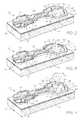
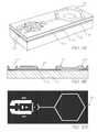
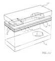
- FIG. 1shows a three dimensional, schematic view of a nozzle assembly for an ink jet printhead
- FIGS. 2 to 4show a three dimensional, schematic illustration of an operation of the nozzle assembly of FIG. 1 ;
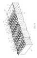
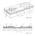
- FIG. 5shows a three dimensional view of a nozzle array constituting an ink jet printhead
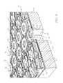
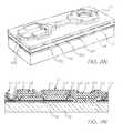
- FIG. 6shows, on an enlarged scale, part of the array of FIG. 5 ;
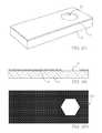
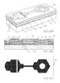
- FIG. 7shows a three dimensional view of an ink jet printhead including a nozzle guard
- FIGS. 8A to 8Rshow three-dimensional views of steps in the manufacture of a nozzle assembly of an ink jet printhead, in accordance with the invention
- FIGS. 9A to 9Rshow sectional side views of the manufacturing steps
- FIGS. 10A to 10Kshow layouts of masks used in various steps in the manufacturing process
- FIGS. 11A to 11Cshow three dimensional views of an operation of the nozzle assembly manufactured according to the method of FIGS. 8 and 9 ;
- FIGS. 12A to 12Cshow sectional side views of an operation of the nozzle assembly manufactured according to the method of FIGS. 8 and 9 .
- a nozzle assemblyin accordance with the invention is designated generally by the reference numeral 10.
- An ink jet printheadhas a plurality of nozzle assemblies 10 arranged in an ink array 14 ( FIGS. 5 and 6 ) on a silicon substrate 16 .
- the array 14will be described in greater detail below.
- the assembly 10includes a silicon substrate or wafer 16 on which a dielectric layer 18 is deposited.
- a CMOS passivation layer 20is deposited on the dielectric layer 18 .
- Each nozzle assembly 12includes a nozzle 22 defining a nozzle opening 24 , a connecting member in the form of a lever arm 26 and an actuator 28 .
- the lever arm 26connects the actuator 28 to the nozzle 22 .
- the nozzle 22comprises a crown portion 30 with a skirt portion 32 depending from the crown portion 30 .
- the skirt portion 32forms part of a peripheral wall of a nozzle chamber 34 ( FIGS. 2 to 4 of the drawings).
- the nozzle opening 24is in fluid communication with the nozzle chamber 34 . It is to be noted that the nozzle opening 24 is surrounded by a raised rim 36 which “pins” a meniscus 38 ( FIG. 2 ) of a body of ink 40 in the nozzle chamber 34 .
- An ink inlet aperture 42(shown most clearly in FIG. 6 of the drawing) is defined in a floor 46 of the nozzle chamber 34 .
- the aperture 42is in fluid communication with an ink inlet channel 48 defined through the substrate 16 .
- a wall portion 50bounds the aperture 42 and extends upwardly from the floor portion 46 .
- the skirt portion 32 , as indicated above, of the nozzle 22defines a first part of a peripheral wall of the nozzle chamber 34 and the wall portion 50 defines a second part of the peripheral wall of the nozzle chamber 34 .
- the wall 50has an inwardly directed lip 52 at its free end which serves as a fluidic seal which inhibits the escape of ink when the nozzle 22 is displaced, as will be described in greater detail below. It will be appreciated that, due to the viscosity of the ink 40 and the small dimensions of the spacing between the lip 52 and the skirt portion 32 , the inwardly directed lip 52 and surface tension function as an effective seal for inhibiting the escape of ink from the nozzle chamber 34 .
- the actuator 28is a thermal bend actuator and is connected to an anchor 54 extending upwardly from the substrate 16 or, more particularly from the CMOS passivation layer 20 .
- the anchor 54is mounted on conductive pads 56 which form an electrical connection with the actuator 28 .
- the actuator 28comprises a first, active beam 58 arranged above a second, passive beam 60 .
- both beams 58 and 60are of, or include, a conductive ceramic material such as titanium nitride (TiN).
- Both beams 58 and 60have their first ends anchored to the anchor 54 and their opposed ends connected to the arm 26 .
- thermal expansion of the beam 58results.
- the passive beam 60through which there is no current flow, does not expand at the same rate, a bending moment is created causing the arm 26 and, hence, the nozzle 22 to be displaced downwardly towards the substrate 16 as shown in FIG. 3 of the drawings.
- Thiscauses an ejection of ink through the nozzle opening 24 as shown at 62 in FIG. 3 of the drawings.
- the source of heatis removed from the active beam 58 , i.e. by stopping current flow, the nozzle 22 returns to its quiescent position as shown in FIG. 4 of the drawings.
- an ink droplet 64is formed as a result of the breaking of an ink droplet neck as illustrated at 66 in FIG. 4 of the drawings.
- the ink droplet 64then travels on to the print media such as a sheet of paper.
- a “negative” meniscusis formed as shown at 68 in FIG. 4 of the drawings.
- This “negative” meniscus 68results in an inflow of ink 40 into the nozzle chamber 34 such that a new meniscus 38 ( FIG. 2 ) is formed in readiness for the next ink drop ejection from the nozzle assembly 10 .
- the array 14is for a four color printhead. Accordingly, the array 14 includes four groups 70 of nozzle assemblies, one for each color. Each group 70 has its nozzle assemblies 10 arranged in two rows 72 and 74 . One of the groups 70 is shown in greater detail in FIG. 6 of the drawings.
- each nozzle assembly 10 in the row 74is offset or staggered with respect to the nozzle assemblies 10 in the row 72 . Also, the nozzle assemblies 10 in the row 72 are spaced apart sufficiently far from each other to enable the lever arms 26 of the nozzle assemblies 10 in the row 74 to pass between adjacent nozzles 22 of the assemblies 10 in the row 72 . It is to be noted that each nozzle assembly 10 is substantially dumbbell shaped so that the nozzles 22 in the row 72 nest between the nozzles 22 and the actuators 28 of adjacent nozzle assemblies 10 in the row 74 .
- each nozzle 22is substantially hexagonally shaped.
- the substrate 16has bond pads 76 arranged thereon which provide the electrical connections, via the pads 56 , to the actuators 28 of the nozzle assemblies 10 . These electrical connections are formed via the CMOS layer (not shown).
- FIG. 7 of the drawingsa development of the invention is shown. With reference to the previous drawings, like reference numerals refer to like parts, unless otherwise specified.
- a nozzle guard 80is mounted on the substrate 16 of the array 14 .
- the nozzle guard 80includes a body member 82 having a plurality of passages 84 defined therethrough.
- the passages 84are in register with the nozzle openings 24 of the nozzle assemblies 10 of the array 14 such that, when ink is ejected from any one of the nozzle openings 24 , the ink passes through the associated passage before striking the print media.
- the body member 82is mounted in spaced relationship relative to the nozzle assemblies 10 by limbs or struts 86 .
- One of the struts 86has air inlet openings 88 defined therein.
- the inkis not entrained in the air as the air is charged through the passages 84 at a different velocity from that of the ink droplets 64 .
- the ink droplets 64are ejected from the nozzles 22 at a velocity of approximately 3 m/s.
- the airis charged through the passages 84 at a velocity of approximately 1 m/s.
- the purpose of the airis to maintain the passages 84 clear of foreign particles. A danger exists that these foreign particles, such as dust particles, could fall onto the nozzle assemblies 10 adversely affecting their operation. With the provision of the air inlet openings 88 in the nozzle guard 80 this problem is, to a large extent, obviated.
- FIGS. 8 to 10 of the drawingsa process for manufacturing the nozzle assemblies 10 is described.
- the dielectric layer 18is deposited on a surface of the wafer 16 .
- the dielectric layer 18is in the form of approximately 1.5 microns of CVD oxide. Resist is spun on to the layer 18 and the layer 18 is exposed to mask 100 and is subsequently developed.
- the layer 18is plasma etched down to the silicon layer 16 .
- the resistis then stripped and the layer 18 is cleaned. This step defines the ink inlet aperture 42 .
- approximately 0.8 microns of aluminum 102is deposited on the layer 18 .
- Resistis spun on and the aluminum 102 is exposed to mask 104 and developed.
- the aluminum 102is plasma etched down to the oxide layer 18 , the resist is stripped and the device is cleaned. This step provides the bond pads and interconnects to the ink jet actuator 28 .
- This interconnectis to an NMOS drive transistor and a power plane with connections made in the CMOS layer (not shown).
- CMOS passivation layer 20Approximately 0.5 microns of PECVD nitride is deposited as the CMOS passivation layer 20 . Resist is spun on and the layer 20 is exposed to mask 106 whereafter it is developed. After development, the nitride is plasma etched down to the aluminum layer 102 and the silicon layer 16 in the region of the inlet aperture 42 . The resist is stripped and the device cleaned.
- a layer 108 of a sacrificial materialis spun on to the layer 20 .
- the layer 108is 6 microns of photo-sensitive polyimide or approximately 4 ⁇ m of high temperature resist.
- the layer 108is softbaked and is then exposed to mask 110 whereafter it is developed.
- the layer 108is then hardbaked at 400° C. for one hour where the layer 108 is comprised of polyimide or at greater than 300° C. where the layer 108 is high temperature resist. It is to be noted in the drawings that the pattern-dependent distortion of the polyimide layer 108 caused by shrinkage is taken into account in the design of the mask 110 .
- a second sacrificial layer 112is applied.
- the layer 112is either 2 ⁇ m of photo-sensitive polyimide which is spun on or approximately 1.3 ⁇ m of high temperature resist.
- the layer 112is softbaked and exposed to mask 114 .
- the layer 112is developed. In the case of the layer 112 being polyimide, the layer 112 is hardbaked at 400° C. for approximately one hour. Where the layer 112 is resist, it is hardbaked at greater than 300° C. for approximately one hour.
- a 0.2 micron multi-layer metal layer 116is then deposited. Part of this layer 116 forms the passive beam 60 of the actuator 28 .
- the layer 116is formed by sputtering 1,000 ⁇ of titanium nitride (TiN) at around 300° C. followed by sputtering 50 ⁇ of tantalum nitride (TaN). A further 1,000 ⁇ of TiN is sputtered on followed by 50 ⁇ of TaN and a further 1,000 ⁇ of TiN.
- TiNtitanium nitride
- TaNtantalum nitride
- TiNtitanium-oxide-semiconductor
- Other materials which can be used instead of TiNare TiB 2 , MoSi 2 or (Ti, Al)N.
- the layer 116is then exposed to mask 118 , developed and plasma etched down to the layer 112 whereafter resist, applied for the layer 116 , is wet stripped taking care not to remove the cured layers 108 or 112 .
- a third sacrificial layer 120is applied by spinning on 4 ⁇ m of photo-sensitive polyimide or approximately 2.6 ⁇ m high temperature resist.
- the layer 120is softbaked whereafter it is exposed to mask 122 .
- the exposed layeris then developed followed by hard baking.
- the layer 120is hardbaked at 400° C. for approximately one hour or at greater than 300° C. where the layer 120 comprises resist.
- a second multi-layer metal layer 124is applied to the layer 120 .
- the constituents of the layer 124are the same as the layer 116 and are applied in the same manner. It will be appreciated that both layers 116 and 124 are electrically conductive layers.
- the layer 124is exposed to mask 126 and is then developed.
- the layer 124is plasma etched down to the polyimide or resist layer 120 whereafter resist applied for the layer 124 is wet stripped taking care not to remove the cured layers 108 , 112 or 120 . It will be noted that the remaining part of the layer 124 defines the active beam 58 of the actuator 28 .
- a fourth sacrificial layer 128is applied by spinning on 4 ⁇ m of photo-sensitive polyimide or approximately 2.6 ⁇ m of high temperature resist.
- the layer 128is softbaked, exposed to the mask 130 and is then developed to leave the island portions as shown in FIG. 9K of the drawings.
- the remaining portions of the layer 128are hardbaked at 400° C. for approximately one hour in the case of polyimide or at greater than 300° C. for resist.
- a high Young's modulus dielectric layer 132is deposited.
- the layer 132is constituted by approximately 1 ⁇ m of silicon nitride or aluminum oxide.
- the layer 132is deposited at a temperature below the hardbaked temperature of the sacrificial layers 108 , 112 , 120 , 128 .
- the primary characteristics required for this dielectric layer 132are a high elastic modulus, chemical inertness and good adhesion to TiN.
- a fifth sacrificial layer 134is applied by spinning on 2 ⁇ m of photo-sensitive polyimide or approximately 1.3 ⁇ m of high temperature resist.
- the layer 134is softbaked, exposed to mask 136 and developed.
- the remaining portion of the layer 134is then hardbaked at 400° C. for one hour in the case of the polyimide or at greater than 300° C. for the resist.
- the dielectric layer 132is plasma etched down to the sacrificial layer 128 taking care not to remove any of the sacrificial layer 134 .
- This stepdefines the nozzle opening 24 , the lever arm 26 and the anchor 54 of the nozzle assembly 10 .
- a high Young's modulus dielectric layer 138is deposited. This layer 138 is formed by depositing 0.2 ⁇ m of silicon nitride or aluminum nitride at a temperature below the hardbaked temperature of the sacrificial layers 108 , 112 , 120 and 128 .
- the layer 138is anisotropically plasma etched to a depth of 0.35 microns. This etch is intended to clear the dielectric from all of the surface except the side walls of the dielectric layer 132 and the sacrificial layer 134 . This step creates the nozzle rim 36 around the nozzle opening 24 which “pins” the meniscus of ink, as described above.
- UV release tape 140is applied. 4 ⁇ m of resist is spun on to a rear of the silicon wafer 16 . The wafer 16 is exposed to mask 142 to back etch the wafer 16 to define the ink inlet channel 48 . The resist is then stripped from the wafer 16 .
- FIGS. 8R and 9R of the drawingsshow the reference numerals illustrated in these two drawings.
- FIGS. 11 and 12show the operation of the nozzle assembly 10 , manufactured in accordance with the process described above with reference to FIGS. 8 and 9 and these figures correspond to FIGS. 2 to 4 of the drawings.
Landscapes
- Engineering & Computer Science (AREA)
- Manufacturing & Machinery (AREA)
- Particle Formation And Scattering Control In Inkjet Printers (AREA)
Abstract
Description
Claims (5)
Priority Applications (1)
| Application Number | Priority Date | Filing Date | Title |
|---|---|---|---|
| US13/295,904US8382251B2 (en) | 2000-05-24 | 2011-11-14 | Nozzle arrangement for printhead |
Applications Claiming Priority (6)
| Application Number | Priority Date | Filing Date | Title |
|---|---|---|---|
| US10/296,435US7169316B1 (en) | 2000-05-24 | 2000-05-24 | Method of manufacture of an ink jet printhead having a moving nozzle with an externally arranged actuator |
| PCT/AU2000/000579WO2001089840A1 (en) | 2000-05-24 | 2000-05-24 | Method of manufacture of an ink jet printhead having a moving nozzle with an externally arranged actuator |
| US11/635,523US7547095B2 (en) | 2000-05-24 | 2006-12-08 | Inkjet printhead having a array of nozzles with external actuators |
| US12/475,557US7887161B2 (en) | 2000-05-24 | 2009-05-31 | Inkjet printhead having an array of displacable nozzles |
| US12/980,181US8070260B2 (en) | 2000-05-24 | 2010-12-28 | Printhead having displacable nozzles |
| US13/295,904US8382251B2 (en) | 2000-05-24 | 2011-11-14 | Nozzle arrangement for printhead |
Related Parent Applications (1)
| Application Number | Title | Priority Date | Filing Date |
|---|---|---|---|
| US12/980,181ContinuationUS8070260B2 (en) | 2000-05-24 | 2010-12-28 | Printhead having displacable nozzles |
Publications (2)
| Publication Number | Publication Date |
|---|---|
| US20120069096A1 US20120069096A1 (en) | 2012-03-22 |
| US8382251B2true US8382251B2 (en) | 2013-02-26 |
Family
ID=3700807
Family Applications (5)
| Application Number | Title | Priority Date | Filing Date |
|---|---|---|---|
| US10/296,435Expired - Fee RelatedUS7169316B1 (en) | 2000-05-24 | 2000-05-24 | Method of manufacture of an ink jet printhead having a moving nozzle with an externally arranged actuator |
| US11/635,523Expired - Fee RelatedUS7547095B2 (en) | 2000-05-24 | 2006-12-08 | Inkjet printhead having a array of nozzles with external actuators |
| US12/475,557Expired - Fee RelatedUS7887161B2 (en) | 2000-05-24 | 2009-05-31 | Inkjet printhead having an array of displacable nozzles |
| US12/980,181Expired - Fee RelatedUS8070260B2 (en) | 2000-05-24 | 2010-12-28 | Printhead having displacable nozzles |
| US13/295,904Expired - Fee RelatedUS8382251B2 (en) | 2000-05-24 | 2011-11-14 | Nozzle arrangement for printhead |
Family Applications Before (4)
| Application Number | Title | Priority Date | Filing Date |
|---|---|---|---|
| US10/296,435Expired - Fee RelatedUS7169316B1 (en) | 2000-05-24 | 2000-05-24 | Method of manufacture of an ink jet printhead having a moving nozzle with an externally arranged actuator |
| US11/635,523Expired - Fee RelatedUS7547095B2 (en) | 2000-05-24 | 2006-12-08 | Inkjet printhead having a array of nozzles with external actuators |
| US12/475,557Expired - Fee RelatedUS7887161B2 (en) | 2000-05-24 | 2009-05-31 | Inkjet printhead having an array of displacable nozzles |
| US12/980,181Expired - Fee RelatedUS8070260B2 (en) | 2000-05-24 | 2010-12-28 | Printhead having displacable nozzles |
Country Status (10)
| Country | Link |
|---|---|
| US (5) | US7169316B1 (en) |
| EP (1) | EP1301345B1 (en) |
| JP (1) | JP4380962B2 (en) |
| CN (2) | CN100398321C (en) |
| AT (1) | ATE367266T1 (en) |
| AU (2) | AU2000247314C1 (en) |
| DE (1) | DE60035618T2 (en) |
| IL (1) | IL166921A (en) |
| WO (1) | WO2001089840A1 (en) |
| ZA (1) | ZA200209795B (en) |
Families Citing this family (15)
| Publication number | Priority date | Publication date | Assignee | Title |
|---|---|---|---|---|
| AUPP398798A0 (en) | 1998-06-09 | 1998-07-02 | Silverbrook Research Pty Ltd | Image creation method and apparatus (ij43) |
| US6513908B2 (en)* | 1997-07-15 | 2003-02-04 | Silverbrook Research Pty Ltd | Pusher actuation in a printhead chip for an inkjet printhead |
| US6792754B2 (en) | 1999-02-15 | 2004-09-21 | Silverbrook Research Pty Ltd | Integrated circuit device for fluid ejection |
| US6526658B1 (en)* | 2000-05-23 | 2003-03-04 | Silverbrook Research Pty Ltd | Method of manufacture of an ink jet printhead having a moving nozzle with an externally arranged actuator |
| JP4380962B2 (en) | 2000-05-24 | 2009-12-09 | シルバーブルック リサーチ ピーティワイ リミテッド | Inkjet printhead manufacturing method |
| US7674671B2 (en) | 2004-12-13 | 2010-03-09 | Optomec Design Company | Aerodynamic jetting of aerosolized fluids for fabrication of passive structures |
| US7938341B2 (en)* | 2004-12-13 | 2011-05-10 | Optomec Design Company | Miniature aerosol jet and aerosol jet array |
| US7605009B2 (en)* | 2007-03-12 | 2009-10-20 | Silverbrook Research Pty Ltd | Method of fabrication MEMS integrated circuits |
| TWI482662B (en) | 2007-08-30 | 2015-05-01 | Optomec Inc | Mechanically integrated and tightly coupled print heads and spray sources |
| EP2738531B1 (en)* | 2012-12-03 | 2015-09-16 | AViTA Corporation | Multi-mode temperature measuring device |
| US20170348903A1 (en)* | 2015-02-10 | 2017-12-07 | Optomec, Inc. | Fabrication of Three-Dimensional Materials Gradient Structures by In-Flight Curing of Aerosols |
| KR102444204B1 (en) | 2015-02-10 | 2022-09-19 | 옵토멕 인코포레이티드 | Method for manufacturing three-dimensional structures by in-flight curing of aerosols |
| CN106903996B (en) | 2017-03-09 | 2020-05-29 | 京东方科技集团股份有限公司 | Printing apparatus |
| CN111655382B (en) | 2017-11-13 | 2022-05-31 | 奥普托美克公司 | Blocking of aerosol flow |
| TW202247905A (en) | 2021-04-29 | 2022-12-16 | 美商阿普托麥克股份有限公司 | High reliability sheathed transport path for aerosol jet devices |
Citations (35)
| Publication number | Priority date | Publication date | Assignee | Title |
|---|---|---|---|---|
| JPS61215059A (en) | 1985-03-22 | 1986-09-24 | Toshiba Corp | Ink jet recording apparatus |
| US4633267A (en) | 1984-12-14 | 1986-12-30 | Siemens Aktiengesellschaft | Arrangement for the ejection of individual droplets from discharge openings of an ink printer head |
| US4718340A (en) | 1982-08-09 | 1988-01-12 | Milliken Research Corporation | Printing method |
| US4736212A (en) | 1985-08-13 | 1988-04-05 | Matsushita Electric Industrial, Co., Ltd. | Ink jet recording apparatus |
| US4975718A (en) | 1987-09-03 | 1990-12-04 | Matsushita Electric Industrial Co., Ltd. | Ink jet recording apparatus |
| EP0416540A2 (en) | 1989-09-05 | 1991-03-13 | Seiko Epson Corporation | Ink jet printer recording head |
| US5051761A (en) | 1990-05-09 | 1991-09-24 | Xerox Corporation | Ink jet printer having a paper handling and maintenance station assembly |
| US5113204A (en) | 1989-04-19 | 1992-05-12 | Seiko Epson Corporation | Ink jet head |
| US5136310A (en) | 1990-09-28 | 1992-08-04 | Xerox Corporation | Thermal ink jet nozzle treatment |
| US5278585A (en) | 1992-05-28 | 1994-01-11 | Xerox Corporation | Ink jet printhead with ink flow directing valves |
| US5374792A (en) | 1993-01-04 | 1994-12-20 | General Electric Company | Micromechanical moving structures including multiple contact switching system |
| JPH0867005A (en) | 1994-08-31 | 1996-03-12 | Fujitsu Ltd | Inkjet head |
| EP0738600A2 (en) | 1995-04-20 | 1996-10-23 | Seiko Epson Corporation | An ink jet head, ink jet recording apparatus, and a control method therefor |
| US5570959A (en) | 1994-10-28 | 1996-11-05 | Fujitsu Limited | Method and system for printing gap adjustment |
| US5665249A (en) | 1994-10-17 | 1997-09-09 | Xerox Corporation | Micro-electromechanical die module with planarized thick film layer |
| WO1998018633A1 (en) | 1996-10-30 | 1998-05-07 | Philips Electronics N.V. | Ink jet printhead and ink jet printer |
| US5828394A (en) | 1995-09-20 | 1998-10-27 | The Board Of Trustees Of The Leland Stanford Junior University | Fluid drop ejector and method |
| WO1999003681A1 (en) | 1997-07-15 | 1999-01-28 | Silverbrook Research Pty. Limited | A thermally actuated ink jet |
| WO1999003680A1 (en) | 1997-07-15 | 1999-01-28 | Silverbrook Research Pty. Limited | A field acutated ink jet |
| US5919548A (en) | 1996-10-11 | 1999-07-06 | Sandia Corporation | Chemical-mechanical polishing of recessed microelectromechanical devices |
| US5922218A (en) | 1995-04-19 | 1999-07-13 | Seiko Epson Corporation | Method of producing ink jet recording head |
| JPH11348311A (en) | 1998-06-04 | 1999-12-21 | Hitachi Koki Co Ltd | Ink purge apparatus and ink purge method for printing press |
| US6168774B1 (en) | 1997-08-07 | 2001-01-02 | Praxair Technology, Inc. | Compact deoxo system |
| US6180427B1 (en) | 1997-07-15 | 2001-01-30 | Silverbrook Research Pty. Ltd. | Method of manufacture of a thermally actuated ink jet including a tapered heater element |
| US6228668B1 (en) | 1997-07-15 | 2001-05-08 | Silverbrook Research Pty Ltd | Method of manufacture of a thermally actuated ink jet printer having a series of thermal actuator units |
| US6254793B1 (en) | 1997-07-15 | 2001-07-03 | Silverbrook Research Pty Ltd | Method of manufacture of high Young's modulus thermoelastic inkjet printer |
| US6261494B1 (en) | 1998-10-22 | 2001-07-17 | Northeastern University | Method of forming plastically deformable microstructures |
| US6382763B1 (en) | 2000-01-24 | 2002-05-07 | Praxair Technology, Inc. | Ink jet printing |
| US6428133B1 (en) | 2000-05-23 | 2002-08-06 | Silverbrook Research Pty Ltd. | Ink jet printhead having a moving nozzle with an externally arranged actuator |
| US6776476B2 (en) | 1997-07-15 | 2004-08-17 | Silverbrook Research Pty Ltd. | Ink jet printhead chip with active and passive nozzle chamber structures |
| US6799828B2 (en) | 2000-05-23 | 2004-10-05 | Silverbrook Research Pty Ltd | Inert gas supply arrangement for a printer |
| US20050157007A1 (en) | 2004-01-21 | 2005-07-21 | Silverbrook Research Pty Ltd. | Pagewidth printhead assembly having a longitudinally extending electrical connector |
| US7066575B2 (en) | 1997-07-15 | 2006-06-27 | Silverbrook Research Pty Ltd | Micro-electromechanical fluid ejection device having a buckle-resistant actuator |
| US7284817B2 (en) | 2000-05-23 | 2007-10-23 | Silverbrook Research Pty Ltd | Printer with a self-cleaning inkjet printhead assembly |
| US7547095B2 (en) | 2000-05-24 | 2009-06-16 | Silverbrook Research Pty Ltd | Inkjet printhead having a array of nozzles with external actuators |
Family Cites Families (1)
| Publication number | Priority date | Publication date | Assignee | Title |
|---|---|---|---|---|
| AUPO794697A0 (en)* | 1997-07-15 | 1997-08-07 | Silverbrook Research Pty Ltd | A device (MEMS10) |
- 2000
- 2000-05-24JPJP2001586058Apatent/JP4380962B2/ennot_activeExpired - Fee Related
- 2000-05-24ATAT00929091Tpatent/ATE367266T1/ennot_activeIP Right Cessation
- 2000-05-24AUAU2000247314Apatent/AU2000247314C1/ennot_activeCeased
- 2000-05-24DEDE60035618Tpatent/DE60035618T2/ennot_activeExpired - Lifetime
- 2000-05-24AUAU4731400Apatent/AU4731400A/enactivePending
- 2000-05-24CNCNB2005100510876Apatent/CN100398321C/ennot_activeExpired - Fee Related
- 2000-05-24WOPCT/AU2000/000579patent/WO2001089840A1/enactiveIP Right Grant
- 2000-05-24CNCN00819574.9Apatent/CN1198726C/ennot_activeExpired - Fee Related
- 2000-05-24EPEP00929091Apatent/EP1301345B1/ennot_activeExpired - Lifetime
- 2000-05-24USUS10/296,435patent/US7169316B1/ennot_activeExpired - Fee Related
- 2002
- 2002-12-03ZAZA200209795Apatent/ZA200209795B/enunknown
- 2005
- 2005-02-15ILIL166921Apatent/IL166921A/ennot_activeIP Right Cessation
- 2006
- 2006-12-08USUS11/635,523patent/US7547095B2/ennot_activeExpired - Fee Related
- 2009
- 2009-05-31USUS12/475,557patent/US7887161B2/ennot_activeExpired - Fee Related
- 2010
- 2010-12-28USUS12/980,181patent/US8070260B2/ennot_activeExpired - Fee Related
- 2011
- 2011-11-14USUS13/295,904patent/US8382251B2/ennot_activeExpired - Fee Related
Patent Citations (40)
| Publication number | Priority date | Publication date | Assignee | Title |
|---|---|---|---|---|
| US4718340A (en) | 1982-08-09 | 1988-01-12 | Milliken Research Corporation | Printing method |
| US4633267A (en) | 1984-12-14 | 1986-12-30 | Siemens Aktiengesellschaft | Arrangement for the ejection of individual droplets from discharge openings of an ink printer head |
| JPS61215059A (en) | 1985-03-22 | 1986-09-24 | Toshiba Corp | Ink jet recording apparatus |
| US4736212A (en) | 1985-08-13 | 1988-04-05 | Matsushita Electric Industrial, Co., Ltd. | Ink jet recording apparatus |
| US4975718A (en) | 1987-09-03 | 1990-12-04 | Matsushita Electric Industrial Co., Ltd. | Ink jet recording apparatus |
| US5113204A (en) | 1989-04-19 | 1992-05-12 | Seiko Epson Corporation | Ink jet head |
| EP0416540A2 (en) | 1989-09-05 | 1991-03-13 | Seiko Epson Corporation | Ink jet printer recording head |
| US5051761A (en) | 1990-05-09 | 1991-09-24 | Xerox Corporation | Ink jet printer having a paper handling and maintenance station assembly |
| US5136310A (en) | 1990-09-28 | 1992-08-04 | Xerox Corporation | Thermal ink jet nozzle treatment |
| US5278585A (en) | 1992-05-28 | 1994-01-11 | Xerox Corporation | Ink jet printhead with ink flow directing valves |
| US5374792A (en) | 1993-01-04 | 1994-12-20 | General Electric Company | Micromechanical moving structures including multiple contact switching system |
| US5454904A (en) | 1993-01-04 | 1995-10-03 | General Electric Company | Micromachining methods for making micromechanical moving structures including multiple contact switching system |
| JPH0867005A (en) | 1994-08-31 | 1996-03-12 | Fujitsu Ltd | Inkjet head |
| US5665249A (en) | 1994-10-17 | 1997-09-09 | Xerox Corporation | Micro-electromechanical die module with planarized thick film layer |
| US5570959A (en) | 1994-10-28 | 1996-11-05 | Fujitsu Limited | Method and system for printing gap adjustment |
| US5922218A (en) | 1995-04-19 | 1999-07-13 | Seiko Epson Corporation | Method of producing ink jet recording head |
| EP0738600A2 (en) | 1995-04-20 | 1996-10-23 | Seiko Epson Corporation | An ink jet head, ink jet recording apparatus, and a control method therefor |
| US5828394A (en) | 1995-09-20 | 1998-10-27 | The Board Of Trustees Of The Leland Stanford Junior University | Fluid drop ejector and method |
| US5919548A (en) | 1996-10-11 | 1999-07-06 | Sandia Corporation | Chemical-mechanical polishing of recessed microelectromechanical devices |
| WO1998018633A1 (en) | 1996-10-30 | 1998-05-07 | Philips Electronics N.V. | Ink jet printhead and ink jet printer |
| US7066575B2 (en) | 1997-07-15 | 2006-06-27 | Silverbrook Research Pty Ltd | Micro-electromechanical fluid ejection device having a buckle-resistant actuator |
| WO1999003681A1 (en) | 1997-07-15 | 1999-01-28 | Silverbrook Research Pty. Limited | A thermally actuated ink jet |
| US6180427B1 (en) | 1997-07-15 | 2001-01-30 | Silverbrook Research Pty. Ltd. | Method of manufacture of a thermally actuated ink jet including a tapered heater element |
| US6228668B1 (en) | 1997-07-15 | 2001-05-08 | Silverbrook Research Pty Ltd | Method of manufacture of a thermally actuated ink jet printer having a series of thermal actuator units |
| US6254793B1 (en) | 1997-07-15 | 2001-07-03 | Silverbrook Research Pty Ltd | Method of manufacture of high Young's modulus thermoelastic inkjet printer |
| WO1999003680A1 (en) | 1997-07-15 | 1999-01-28 | Silverbrook Research Pty. Limited | A field acutated ink jet |
| US6776476B2 (en) | 1997-07-15 | 2004-08-17 | Silverbrook Research Pty Ltd. | Ink jet printhead chip with active and passive nozzle chamber structures |
| US6168774B1 (en) | 1997-08-07 | 2001-01-02 | Praxair Technology, Inc. | Compact deoxo system |
| JPH11348311A (en) | 1998-06-04 | 1999-12-21 | Hitachi Koki Co Ltd | Ink purge apparatus and ink purge method for printing press |
| US6261494B1 (en) | 1998-10-22 | 2001-07-17 | Northeastern University | Method of forming plastically deformable microstructures |
| US6382763B1 (en) | 2000-01-24 | 2002-05-07 | Praxair Technology, Inc. | Ink jet printing |
| US6428133B1 (en) | 2000-05-23 | 2002-08-06 | Silverbrook Research Pty Ltd. | Ink jet printhead having a moving nozzle with an externally arranged actuator |
| US6799828B2 (en) | 2000-05-23 | 2004-10-05 | Silverbrook Research Pty Ltd | Inert gas supply arrangement for a printer |
| US7284817B2 (en) | 2000-05-23 | 2007-10-23 | Silverbrook Research Pty Ltd | Printer with a self-cleaning inkjet printhead assembly |
| US7465028B2 (en) | 2000-05-23 | 2008-12-16 | Silverbrook Research Pty Ltd | Nozzle assembly having a thermal actuator with active and passive beams |
| US7654644B2 (en) | 2000-05-23 | 2010-02-02 | Silverbrook Research Pty Ltd | Printhead nozzle arrangement having variable volume nozzle chamber |
| US7547095B2 (en) | 2000-05-24 | 2009-06-16 | Silverbrook Research Pty Ltd | Inkjet printhead having a array of nozzles with external actuators |
| US7887161B2 (en) | 2000-05-24 | 2011-02-15 | Silverbrook Research Pty Ltd | Inkjet printhead having an array of displacable nozzles |
| US8070260B2 (en)* | 2000-05-24 | 2011-12-06 | Silverbrook Research Pty Ltd | Printhead having displacable nozzles |
| US20050157007A1 (en) | 2004-01-21 | 2005-07-21 | Silverbrook Research Pty Ltd. | Pagewidth printhead assembly having a longitudinally extending electrical connector |
Also Published As
| Publication number | Publication date |
|---|---|
| JP2003534168A (en) | 2003-11-18 |
| EP1301345A4 (en) | 2004-11-17 |
| US7547095B2 (en) | 2009-06-16 |
| DE60035618D1 (en) | 2007-08-30 |
| CN1452554A (en) | 2003-10-29 |
| CN100398321C (en) | 2008-07-02 |
| WO2001089840A1 (en) | 2001-11-29 |
| ATE367266T1 (en) | 2007-08-15 |
| US20110090285A1 (en) | 2011-04-21 |
| ZA200209795B (en) | 2003-07-30 |
| AU2000247314C1 (en) | 2005-10-06 |
| US7887161B2 (en) | 2011-02-15 |
| DE60035618T2 (en) | 2008-07-03 |
| AU4731400A (en) | 2001-12-03 |
| JP4380962B2 (en) | 2009-12-09 |
| US8070260B2 (en) | 2011-12-06 |
| CN1198726C (en) | 2005-04-27 |
| US20070080980A1 (en) | 2007-04-12 |
| US7169316B1 (en) | 2007-01-30 |
| EP1301345B1 (en) | 2007-07-18 |
| IL166921A (en) | 2010-05-31 |
| US20090237449A1 (en) | 2009-09-24 |
| US20120069096A1 (en) | 2012-03-22 |
| EP1301345A1 (en) | 2003-04-16 |
| CN1651244A (en) | 2005-08-10 |
| AU2000247314B2 (en) | 2004-10-21 |
Similar Documents
| Publication | Publication Date | Title |
|---|---|---|
| US6526658B1 (en) | Method of manufacture of an ink jet printhead having a moving nozzle with an externally arranged actuator | |
| US8382251B2 (en) | Nozzle arrangement for printhead | |
| US7766459B2 (en) | Multi-coloured printhead nozzle array with rows of nozzle assemblies | |
| US7984968B2 (en) | Inkjet printhead nozzle assembly having a raised rim to support an ink meniscus | |
| US7581817B2 (en) | Inkjet nozzle assembly with a raised rim for pinning a meniscus of ink in a nozzle chamber | |
| AU2000247313A1 (en) | Ink jet printhead having a moving nozzle with an externally arranged actuator | |
| US6328417B1 (en) | Ink jet printhead nozzle array | |
| US6428133B1 (en) | Ink jet printhead having a moving nozzle with an externally arranged actuator | |
| AU2000247314A1 (en) | Method of manufacture of an ink jet printhead having a moving nozzle with an externally arranged actuator | |
| US7021744B2 (en) | Printhead assembly having nozzle guard | |
| US8075095B2 (en) | Inkjet printhead with moving nozzle openings | |
| AU2005200212B2 (en) | Ink jet nozzle assembly with externally arranged nozzle actuator | |
| US7018016B1 (en) | Fluidic seal for an ink jet nozzle assembly |
Legal Events
| Date | Code | Title | Description |
|---|---|---|---|
| AS | Assignment | Owner name:SILVERBROOK RESEARCH PTY LTD, AUSTRALIA Free format text:ASSIGNMENT OF ASSIGNORS INTEREST;ASSIGNOR:SILVERBROOK, KIA;REEL/FRAME:027223/0477 Effective date:20090311 | |
| STCF | Information on status: patent grant | Free format text:PATENTED CASE | |
| AS | Assignment | Owner name:ZAMTEC LIMITED, IRELAND Free format text:ASSIGNMENT OF ASSIGNORS INTEREST;ASSIGNOR:SILVERBROOK RESEARCH PTY. LIMITED;REEL/FRAME:030169/0193 Effective date:20120503 | |
| AS | Assignment | Owner name:MEMJET TECHNOLOGY LIMITED, IRELAND Free format text:CHANGE OF NAME;ASSIGNOR:ZAMTEC LIMITED;REEL/FRAME:033244/0276 Effective date:20140609 | |
| FPAY | Fee payment | Year of fee payment:4 | |
| FEPP | Fee payment procedure | Free format text:MAINTENANCE FEE REMINDER MAILED (ORIGINAL EVENT CODE: REM.); ENTITY STATUS OF PATENT OWNER: LARGE ENTITY | |
| LAPS | Lapse for failure to pay maintenance fees | Free format text:PATENT EXPIRED FOR FAILURE TO PAY MAINTENANCE FEES (ORIGINAL EVENT CODE: EXP.); ENTITY STATUS OF PATENT OWNER: LARGE ENTITY | |
| STCH | Information on status: patent discontinuation | Free format text:PATENT EXPIRED DUE TO NONPAYMENT OF MAINTENANCE FEES UNDER 37 CFR 1.362 | |
| FP | Lapsed due to failure to pay maintenance fee | Effective date:20210226 |