US8379012B2 - Selector switch for direct connection of switched regulator to voltage inputs - Google Patents
Selector switch for direct connection of switched regulator to voltage inputsDownload PDFInfo
- Publication number
- US8379012B2 US8379012B2US12/505,190US50519009AUS8379012B2US 8379012 B2US8379012 B2US 8379012B2US 50519009 AUS50519009 AUS 50519009AUS 8379012 B2US8379012 B2US 8379012B2
- Authority
- US
- United States
- Prior art keywords
- voltage
- coupled
- display device
- output
- switched regulator
- Prior art date
- Legal status (The legal status is an assumption and is not a legal conclusion. Google has not performed a legal analysis and makes no representation as to the accuracy of the status listed.)
- Active, expires
Links
Images


Classifications
- G—PHYSICS
- G06—COMPUTING OR CALCULATING; COUNTING
- G06F—ELECTRIC DIGITAL DATA PROCESSING
- G06F1/00—Details not covered by groups G06F3/00 - G06F13/00 and G06F21/00
- G06F1/26—Power supply means, e.g. regulation thereof
- G06F1/32—Means for saving power
- G06F1/3203—Power management, i.e. event-based initiation of a power-saving mode
- G06F1/3206—Monitoring of events, devices or parameters that trigger a change in power modality
- G06F1/3215—Monitoring of peripheral devices
- G06F1/3218—Monitoring of peripheral devices of display devices
- H—ELECTRICITY
- H02—GENERATION; CONVERSION OR DISTRIBUTION OF ELECTRIC POWER
- H02M—APPARATUS FOR CONVERSION BETWEEN AC AND AC, BETWEEN AC AND DC, OR BETWEEN DC AND DC, AND FOR USE WITH MAINS OR SIMILAR POWER SUPPLY SYSTEMS; CONVERSION OF DC OR AC INPUT POWER INTO SURGE OUTPUT POWER; CONTROL OR REGULATION THEREOF
- H02M3/00—Conversion of DC power input into DC power output
- H02M3/02—Conversion of DC power input into DC power output without intermediate conversion into AC
- H02M3/04—Conversion of DC power input into DC power output without intermediate conversion into AC by static converters
- H02M3/10—Conversion of DC power input into DC power output without intermediate conversion into AC by static converters using discharge tubes with control electrode or semiconductor devices with control electrode
- H02M3/145—Conversion of DC power input into DC power output without intermediate conversion into AC by static converters using discharge tubes with control electrode or semiconductor devices with control electrode using devices of a triode or transistor type requiring continuous application of a control signal
- H02M3/155—Conversion of DC power input into DC power output without intermediate conversion into AC by static converters using discharge tubes with control electrode or semiconductor devices with control electrode using devices of a triode or transistor type requiring continuous application of a control signal using semiconductor devices only
- H02M3/156—Conversion of DC power input into DC power output without intermediate conversion into AC by static converters using discharge tubes with control electrode or semiconductor devices with control electrode using devices of a triode or transistor type requiring continuous application of a control signal using semiconductor devices only with automatic control of output voltage or current, e.g. switching regulators
Definitions
- This subject matteris generally related to electronics, and more particularly to a driver circuit for a display device, such as a Liquid Crystal Display (LCD).
- a display devicesuch as a Liquid Crystal Display (LCD).
- LCDLiquid Crystal Display
- a conventional LCD panelusually requires several different voltage levels dependent on the complexity of the LCD panel. These different voltage levels can be accomplished by dividing a high voltage provided at the output of a switched regulator (e.g., capacitor or inductor) by some means (e.g., a resistor ladder). The divided voltages can be optionally driven by buffers for better power efficiency. If the LCD panel is small or the power consumption is not important the buffers can be omitted by sizing the resistor string appropriately. The voltages can be smoothed by decoupling capacitors or omitted if power efficiency is not required.
- the high voltage output by the switched regulatoris generally controlled by a voltage divider which, in turn, controls the contrast of the LCD panel.
- the voltage divider and resistor stringcan be combined into a single circuit.
- a comparatorcan be used to turn on the switched regulator and increase the high voltage output by the switched regulator to the desire level required by the LCD panel.
- powercan be lost in the switched regulator, the resistor string, the voltage divider and the buffers.
- a driver circuit for a display deviceomits buffers and a resistive ladder and connects the output of a switched regulator directly to a display device through a selector switch.
- Voltage inputs for the display devicecan be selectively coupled to the output of the switched regulator using the selector switch.
- Each voltage inputcan be coupled to a capacitor that is charged when the corresponding voltage input is coupled to the high voltage output of the switched regulator.
- bypass switchesare connected between the voltage inputs. If the voltage of a given capacitor is too high, the excess voltage can be transferred or otherwise discharged through the bypass switch to another capacitor storing a lower voltage.
- driver circuitsboost the voltage and then divide the boosted voltage through a resistive ladder and optionally buffers which can waste energy.
- the disclosed driver circuitomits buffers and a resistive ladder.
- the high voltage output of the switched regulatoris coupled directly to the voltage input terminals of the display device, thus conserving energy that would otherwise be lost due to buffers and a resistive ladder.
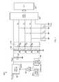
- FIG. 1is a schematic diagram of a display driver including a switched regulator coupled to a switch network through a resistive ladder and buffers.
- FIG. 2is a schematic diagram of an exemplary display driver including a switched regulator coupled directly to a switch network.
- FIG. 3is a schematic diagram of an exemplary inductive-type switched regulator.
- FIG. 4is a flow diagram of an exemplary process for switching boosted voltage to a display device.
- FIG. 1is a schematic diagram of display driver, including a switched regulator coupled to a switch network through a resistive ladder and buffers.
- display driver 100can include switched regulator 102 , voltage reference 104 , voltage divider 106 , comparator 107 , resistive ladder 108 , buffers 110 , decoupling capacitors 112 , smoothing capacitor 114 , switch network 116 and display device 118 .
- Display device 118(e.g., an LCD panel) is configured to use several different voltage levels based on the design of display device 118 .
- the different voltage levelscan be provided by dividing a high voltage output of switched regulator 102 , V HIGH , by resistive ladder 108 (R 1 -R 4 ).
- resistive ladder 108R 1 -R 4
- display device 118uses five voltages ( 0 , V 1 , V 2 , V 3 , V HIGH ).
- the divided voltagesare driven by buffers 110 (B 1 -B 3 ) for better power efficiency. If the display device is small or the power consumption is not important buffers 110 can be omitted by sizing resistive ladder 108 appropriately.
- the voltagescan be smoothed by decoupling capacitors 12 (C 1 -C 3 ). If power efficiency is not required the decoupling capacitors can be omitted.
- Capacitor 114(C 4 ) can be used for smoothing high voltage output from switched regulator 102 .
- the output voltage, V HIGHcan be controlled by voltage divider 106 which, in turn, can control the contrast of the display device 118 .
- voltage divider 106 and resistive ladder 108can be combined.
- comparator 107turns on switched regulator 102 and increases V HIGH to a desired level. In this example, an on/off regulator control is used. Other means of control duty cycle is possible.
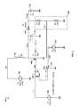
- FIG. 2is a schematic diagram of an exemplary display driver, including a switched regulator coupled directly to a switch network.
- display driver 200can include switched regulator 202 , voltage reference 204 , voltage divider 206 , comparator 207 , decoupling capacitors 208 , bypass switches 210 , selector switch control 212 , switch network 216 and display device 218 .
- Display driver 200omits buffers 110 and connects the output from switched regulator 202 directly to switch network 214 and display device 216 through selector switch 212 .
- the voltages V 1 -V 4are controlled directly by adjusting the contrast control for each voltage input (e.g., using voltage divider 206 ).
- Selector switch 212selects one output at a time and charges or optionally discharges decoupling capacitors 208 (C 1 -C 4 ) as required. If decoupling capacitors 208 are small, switched regulator 102 can update decoupling capacitors 208 often and the resulting switching losses can be larger.
- a key advantage with display driver 200is that there is no longer power loss due to buffers.
- bypass switches 210can be included for connecting between different voltage inputs. For example, if a given decoupling capacitor voltage is too high, the excess voltage can be transferred or discharged to another decoupling capacitor which has a lower voltage. The switching can be controlled by selector switch 212 or another controller or logic. Similar to capacitor C 4 in display driver 100 , the capacitor C 4 can be used as a smoothing capacitor for output voltage V HIGH .
- Selector switch 212can be implemented using hardware and/or software.
- selector switchcan be implemented using a controller or logic.
- Selector switch 212can be operated based on a state machine or software or firmware instructions.
- FIG. 3is a schematic diagram of an exemplary inductive-type switched regulator.
- an inductive-type switched regulator 202includes voltage source 302 (V 1 ), clock 304 (V 3 ), gate 306 (A 3 ), transistor 308 (X 1 ), inductor 310 (L 1 ), comparator 312 (U 1 ), capacitor 314 (C 4 ), voltage reference 316 (V 2 ), diode 318 (D 1 ), voltage divider 320 (R 2 , R 3 ) and capacitor 324 (C 2 ).
- a small and simple inductive boost regulator 202can be used in display driver 200 .
- comparator 312 outputis high and transistor 308 is turned on and off through gate 306 with a frequency set by clock 304 .
- transistor 308is turned on capacitor 314 charges.
- Diode 318 in combination with capacitor 322provides a DC output voltage V HIGH , which can be supplied to switch network 214 .
- the voltage dividercan include resistors 320 , 322 which can be set so that the output voltage V OUT is V volts (e.g., 5 volts).
- the voltage divider 320 in this example circuitis resistive but in some circuits a capacitive voltage divider can be used to save current consumption and silicon area.
- Capacitor 322smoothes the output voltage V OUT .
- FIG. 4is a flow diagram of an exemplary process for switching boosted voltage to a display device.
- a process 400can begin by applying a voltage supply to an input of a switched regulator ( 402 ).
- the switched regulatorboosts the voltage to a desired level ( 404 ).
- the switched regulatorcan be a capacitive-type or inductive-type switched regulator.
- a selector switchcan be configured to selectively couple the output of the switched regulator directly to a voltage input of a switch network ( 406 ).
- the switch networkcan couple the boosted voltage to a display device ( 408 ).
- a decoupling capacitorcan be coupled to each voltage input of the switch network and can store the boosted voltage output by the switched regulator.
Landscapes
- Engineering & Computer Science (AREA)
- Theoretical Computer Science (AREA)
- Physics & Mathematics (AREA)
- General Engineering & Computer Science (AREA)
- General Physics & Mathematics (AREA)
- Power Engineering (AREA)
- Control Of Indicators Other Than Cathode Ray Tubes (AREA)
Abstract
Description
POUT=VOUT*IOUT. (1)
PIN=VHIGH*IIN, (2)
and the efficiency is given by as
IOUT=IIN−IBUFFER=α*IIN, (4)
where α is the efficiency of
Claims (12)
Priority Applications (1)
| Application Number | Priority Date | Filing Date | Title |
|---|---|---|---|
| US12/505,190US8379012B2 (en) | 2009-07-17 | 2009-07-17 | Selector switch for direct connection of switched regulator to voltage inputs |
Applications Claiming Priority (1)
| Application Number | Priority Date | Filing Date | Title |
|---|---|---|---|
| US12/505,190US8379012B2 (en) | 2009-07-17 | 2009-07-17 | Selector switch for direct connection of switched regulator to voltage inputs |
Publications (2)
| Publication Number | Publication Date |
|---|---|
| US20110012886A1 US20110012886A1 (en) | 2011-01-20 |
| US8379012B2true US8379012B2 (en) | 2013-02-19 |
Family
ID=43464944
Family Applications (1)
| Application Number | Title | Priority Date | Filing Date |
|---|---|---|---|
| US12/505,190Active2031-12-01US8379012B2 (en) | 2009-07-17 | 2009-07-17 | Selector switch for direct connection of switched regulator to voltage inputs |
Country Status (1)
| Country | Link |
|---|---|
| US (1) | US8379012B2 (en) |
Cited By (1)
| Publication number | Priority date | Publication date | Assignee | Title |
|---|---|---|---|---|
| US20170187280A1 (en)* | 2015-12-28 | 2017-06-29 | Allegro Microsystems, Llc | Compensating For Voltage Changes In Driver Circuits |
Families Citing this family (2)
| Publication number | Priority date | Publication date | Assignee | Title |
|---|---|---|---|---|
| CN102255395B (en)* | 2011-06-27 | 2014-11-05 | 华为终端有限公司 | Electronic equipment and method for supplying power to at least two different loads by single power supply |
| GB201714325D0 (en)* | 2017-09-06 | 2017-10-18 | Nordic Semiconductor Asa | Power Supply Circuits |
Citations (8)
| Publication number | Priority date | Publication date | Assignee | Title |
|---|---|---|---|---|
| US4694350A (en)* | 1985-10-01 | 1987-09-15 | Rca Corporation | Automatic bias control of an image display device in a video monitor |
| US5130703A (en)* | 1989-06-30 | 1992-07-14 | Poqet Computer Corp. | Power system and scan method for liquid crystal display |
| US5331354A (en)* | 1990-09-26 | 1994-07-19 | Matsushita Electric Industrial Co., Ltd. | Power supply apparatus for television receiver set and television receiver set including the same |
| US20080191976A1 (en)* | 2004-06-29 | 2008-08-14 | Arokia Nathan | Voltage-Programming Scheme for Current-Driven Arnoled Displays |
| US20080316154A1 (en)* | 2007-06-22 | 2008-12-25 | Hyoung-Rae Kim | Apparatus and method for generating VCOM voltage in display device |
| US7675245B2 (en)* | 2007-01-04 | 2010-03-09 | Allegro Microsystems, Inc. | Electronic circuit for driving a diode load |
| US20110128303A1 (en)* | 2009-05-19 | 2011-06-02 | Rohm Co., Ltd. | Driving circuit for light emitting diode |
| US8125431B2 (en)* | 2007-06-18 | 2012-02-28 | Sony Corporation | Electro-optical device and electronic apparatus |
- 2009
- 2009-07-17USUS12/505,190patent/US8379012B2/enactiveActive
Patent Citations (8)
| Publication number | Priority date | Publication date | Assignee | Title |
|---|---|---|---|---|
| US4694350A (en)* | 1985-10-01 | 1987-09-15 | Rca Corporation | Automatic bias control of an image display device in a video monitor |
| US5130703A (en)* | 1989-06-30 | 1992-07-14 | Poqet Computer Corp. | Power system and scan method for liquid crystal display |
| US5331354A (en)* | 1990-09-26 | 1994-07-19 | Matsushita Electric Industrial Co., Ltd. | Power supply apparatus for television receiver set and television receiver set including the same |
| US20080191976A1 (en)* | 2004-06-29 | 2008-08-14 | Arokia Nathan | Voltage-Programming Scheme for Current-Driven Arnoled Displays |
| US7675245B2 (en)* | 2007-01-04 | 2010-03-09 | Allegro Microsystems, Inc. | Electronic circuit for driving a diode load |
| US8125431B2 (en)* | 2007-06-18 | 2012-02-28 | Sony Corporation | Electro-optical device and electronic apparatus |
| US20080316154A1 (en)* | 2007-06-22 | 2008-12-25 | Hyoung-Rae Kim | Apparatus and method for generating VCOM voltage in display device |
| US20110128303A1 (en)* | 2009-05-19 | 2011-06-02 | Rohm Co., Ltd. | Driving circuit for light emitting diode |
Cited By (2)
| Publication number | Priority date | Publication date | Assignee | Title |
|---|---|---|---|---|
| US20170187280A1 (en)* | 2015-12-28 | 2017-06-29 | Allegro Microsystems, Llc | Compensating For Voltage Changes In Driver Circuits |
| US9825528B2 (en)* | 2015-12-28 | 2017-11-21 | Allegro Microsystems, Llc | Compensating for voltage changes in driver circuits |
Also Published As
| Publication number | Publication date |
|---|---|
| US20110012886A1 (en) | 2011-01-20 |
Similar Documents
| Publication | Publication Date | Title |
|---|---|---|
| US6147477A (en) | DC to DC converter producing output voltage exhibiting rise and fall characteristics independent of load thereon | |
| US8736247B2 (en) | Power supply circuit and control method of controlling the power supply circuit | |
| KR100503187B1 (en) | Driving device for display device | |
| CN100390853C (en) | High-efficiency liquid crystal display driving voltage generating circuit and method thereof | |
| US6738272B2 (en) | Charge pump rush current limiting circuit | |
| US7888920B2 (en) | Power supply device with fast output voltage switching capability | |
| US20090261888A1 (en) | Autonomous control of multiple supply voltage generators for display drivers | |
| US8471486B2 (en) | Energy-saving mechanisms in multi-color display devices | |
| CN107342695A (en) | Synchronous rectifier | |
| CN101873064B (en) | Boost circuit and liquid crystal display device using boost circuit | |
| US5568016A (en) | Power supply for an electroluminescent panel or the like | |
| US9332602B2 (en) | LED driver with transformerless hysteretic boost | |
| US8379012B2 (en) | Selector switch for direct connection of switched regulator to voltage inputs | |
| CN101303823A (en) | Voltage supply circuit and related method thereof | |
| US20080265861A1 (en) | Voltage providing circuit and related method thereof | |
| KR101129287B1 (en) | LED Driving System | |
| CN101540549A (en) | Voltage regulation type charge pump | |
| US10582577B2 (en) | LED drive circuit | |
| KR100296007B1 (en) | Driving method of piezoelecric transformer and driving circuit for the same | |
| KR100920957B1 (en) | Soft Start Circuit of Power Supply | |
| CN100410742C (en) | Converter controller having feedforward compensation, converting system and method for controlling same | |
| US5914870A (en) | Low power high efficiency power supply | |
| US20190173383A1 (en) | Buck-boost converter power supply with drive circuit | |
| CN110138206A (en) | Power driving circuit and display device | |
| US7915880B2 (en) | Step-up DC-DC converter |
Legal Events
| Date | Code | Title | Description |
|---|---|---|---|
| AS | Assignment | Owner name:ATMEL CORPORATION, CALIFORNIA Free format text:ASSIGNMENT OF ASSIGNORS INTEREST;ASSIGNORS:SAETHER, TERJE;LUND, MORTEN WERNER;REEL/FRAME:023316/0357 Effective date:20090717 | |
| STCF | Information on status: patent grant | Free format text:PATENTED CASE | |
| AS | Assignment | Owner name:MORGAN STANLEY SENIOR FUNDING, INC. AS ADMINISTRATIVE AGENT, NEW YORK Free format text:PATENT SECURITY AGREEMENT;ASSIGNOR:ATMEL CORPORATION;REEL/FRAME:031912/0173 Effective date:20131206 Owner name:MORGAN STANLEY SENIOR FUNDING, INC. AS ADMINISTRAT Free format text:PATENT SECURITY AGREEMENT;ASSIGNOR:ATMEL CORPORATION;REEL/FRAME:031912/0173 Effective date:20131206 | |
| AS | Assignment | Owner name:ATMEL CORPORATION, CALIFORNIA Free format text:TERMINATION AND RELEASE OF SECURITY INTEREST IN PATENT COLLATERAL;ASSIGNOR:MORGAN STANLEY SENIOR FUNDING, INC.;REEL/FRAME:038376/0001 Effective date:20160404 | |
| FPAY | Fee payment | Year of fee payment:4 | |
| AS | Assignment | Owner name:JPMORGAN CHASE BANK, N.A., AS ADMINISTRATIVE AGENT, ILLINOIS Free format text:SECURITY INTEREST;ASSIGNOR:ATMEL CORPORATION;REEL/FRAME:041715/0747 Effective date:20170208 Owner name:JPMORGAN CHASE BANK, N.A., AS ADMINISTRATIVE AGENT Free format text:SECURITY INTEREST;ASSIGNOR:ATMEL CORPORATION;REEL/FRAME:041715/0747 Effective date:20170208 | |
| AS | Assignment | Owner name:JPMORGAN CHASE BANK, N.A., AS ADMINISTRATIVE AGENT, ILLINOIS Free format text:SECURITY INTEREST;ASSIGNORS:MICROCHIP TECHNOLOGY INCORPORATED;SILICON STORAGE TECHNOLOGY, INC.;ATMEL CORPORATION;AND OTHERS;REEL/FRAME:046426/0001 Effective date:20180529 Owner name:JPMORGAN CHASE BANK, N.A., AS ADMINISTRATIVE AGENT Free format text:SECURITY INTEREST;ASSIGNORS:MICROCHIP TECHNOLOGY INCORPORATED;SILICON STORAGE TECHNOLOGY, INC.;ATMEL CORPORATION;AND OTHERS;REEL/FRAME:046426/0001 Effective date:20180529 | |
| AS | Assignment | Owner name:WELLS FARGO BANK, NATIONAL ASSOCIATION, AS NOTES COLLATERAL AGENT, CALIFORNIA Free format text:SECURITY INTEREST;ASSIGNORS:MICROCHIP TECHNOLOGY INCORPORATED;SILICON STORAGE TECHNOLOGY, INC.;ATMEL CORPORATION;AND OTHERS;REEL/FRAME:047103/0206 Effective date:20180914 Owner name:WELLS FARGO BANK, NATIONAL ASSOCIATION, AS NOTES C Free format text:SECURITY INTEREST;ASSIGNORS:MICROCHIP TECHNOLOGY INCORPORATED;SILICON STORAGE TECHNOLOGY, INC.;ATMEL CORPORATION;AND OTHERS;REEL/FRAME:047103/0206 Effective date:20180914 | |
| AS | Assignment | Owner name:JPMORGAN CHASE BANK, N.A., AS ADMINISTRATIVE AGENT, DELAWARE Free format text:SECURITY INTEREST;ASSIGNORS:MICROCHIP TECHNOLOGY INC.;SILICON STORAGE TECHNOLOGY, INC.;ATMEL CORPORATION;AND OTHERS;REEL/FRAME:053311/0305 Effective date:20200327 | |
| AS | Assignment | Owner name:MICROSEMI STORAGE SOLUTIONS, INC., ARIZONA Free format text:RELEASE BY SECURED PARTY;ASSIGNOR:JPMORGAN CHASE BANK, N.A, AS ADMINISTRATIVE AGENT;REEL/FRAME:053466/0011 Effective date:20200529 Owner name:MICROSEMI CORPORATION, CALIFORNIA Free format text:RELEASE BY SECURED PARTY;ASSIGNOR:JPMORGAN CHASE BANK, N.A, AS ADMINISTRATIVE AGENT;REEL/FRAME:053466/0011 Effective date:20200529 Owner name:ATMEL CORPORATION, ARIZONA Free format text:RELEASE BY SECURED PARTY;ASSIGNOR:JPMORGAN CHASE BANK, N.A, AS ADMINISTRATIVE AGENT;REEL/FRAME:053466/0011 Effective date:20200529 Owner name:MICROCHIP TECHNOLOGY INC., ARIZONA Free format text:RELEASE BY SECURED PARTY;ASSIGNOR:JPMORGAN CHASE BANK, N.A, AS ADMINISTRATIVE AGENT;REEL/FRAME:053466/0011 Effective date:20200529 Owner name:SILICON STORAGE TECHNOLOGY, INC., ARIZONA Free format text:RELEASE BY SECURED PARTY;ASSIGNOR:JPMORGAN CHASE BANK, N.A, AS ADMINISTRATIVE AGENT;REEL/FRAME:053466/0011 Effective date:20200529 | |
| AS | Assignment | Owner name:WELLS FARGO BANK, NATIONAL ASSOCIATION, MINNESOTA Free format text:SECURITY INTEREST;ASSIGNORS:MICROCHIP TECHNOLOGY INC.;SILICON STORAGE TECHNOLOGY, INC.;ATMEL CORPORATION;AND OTHERS;REEL/FRAME:053468/0705 Effective date:20200529 | |
| MAFP | Maintenance fee payment | Free format text:PAYMENT OF MAINTENANCE FEE, 8TH YEAR, LARGE ENTITY (ORIGINAL EVENT CODE: M1552); ENTITY STATUS OF PATENT OWNER: LARGE ENTITY Year of fee payment:8 | |
| AS | Assignment | Owner name:WELLS FARGO BANK, NATIONAL ASSOCIATION, AS COLLATERAL AGENT, MINNESOTA Free format text:SECURITY INTEREST;ASSIGNORS:MICROCHIP TECHNOLOGY INCORPORATED;SILICON STORAGE TECHNOLOGY, INC.;ATMEL CORPORATION;AND OTHERS;REEL/FRAME:055671/0612 Effective date:20201217 | |
| AS | Assignment | Owner name:WELLS FARGO BANK, NATIONAL ASSOCIATION, AS NOTES COLLATERAL AGENT, MINNESOTA Free format text:SECURITY INTEREST;ASSIGNORS:MICROCHIP TECHNOLOGY INCORPORATED;SILICON STORAGE TECHNOLOGY, INC.;ATMEL CORPORATION;AND OTHERS;REEL/FRAME:057935/0474 Effective date:20210528 | |
| AS | Assignment | Owner name:MICROSEMI STORAGE SOLUTIONS, INC., ARIZONA Free format text:RELEASE BY SECURED PARTY;ASSIGNOR:JPMORGAN CHASE BANK, N.A., AS ADMINISTRATIVE AGENT;REEL/FRAME:059333/0222 Effective date:20220218 Owner name:MICROSEMI CORPORATION, ARIZONA Free format text:RELEASE BY SECURED PARTY;ASSIGNOR:JPMORGAN CHASE BANK, N.A., AS ADMINISTRATIVE AGENT;REEL/FRAME:059333/0222 Effective date:20220218 Owner name:ATMEL CORPORATION, ARIZONA Free format text:RELEASE BY SECURED PARTY;ASSIGNOR:JPMORGAN CHASE BANK, N.A., AS ADMINISTRATIVE AGENT;REEL/FRAME:059333/0222 Effective date:20220218 Owner name:SILICON STORAGE TECHNOLOGY, INC., ARIZONA Free format text:RELEASE BY SECURED PARTY;ASSIGNOR:JPMORGAN CHASE BANK, N.A., AS ADMINISTRATIVE AGENT;REEL/FRAME:059333/0222 Effective date:20220218 Owner name:MICROCHIP TECHNOLOGY INCORPORATED, ARIZONA Free format text:RELEASE BY SECURED PARTY;ASSIGNOR:JPMORGAN CHASE BANK, N.A., AS ADMINISTRATIVE AGENT;REEL/FRAME:059333/0222 Effective date:20220218 | |
| AS | Assignment | Owner name:ATMEL CORPORATION, ARIZONA Free format text:RELEASE BY SECURED PARTY;ASSIGNOR:JPMORGAN CHASE BANK, N.A., AS ADMINISTRATIVE AGENT;REEL/FRAME:059262/0105 Effective date:20220218 | |
| AS | Assignment | Owner name:MICROSEMI STORAGE SOLUTIONS, INC., ARIZONA Free format text:RELEASE BY SECURED PARTY;ASSIGNOR:WELLS FARGO BANK, NATIONAL ASSOCIATION, AS NOTES COLLATERAL AGENT;REEL/FRAME:059358/0001 Effective date:20220228 Owner name:MICROSEMI CORPORATION, ARIZONA Free format text:RELEASE BY SECURED PARTY;ASSIGNOR:WELLS FARGO BANK, NATIONAL ASSOCIATION, AS NOTES COLLATERAL AGENT;REEL/FRAME:059358/0001 Effective date:20220228 Owner name:ATMEL CORPORATION, ARIZONA Free format text:RELEASE BY SECURED PARTY;ASSIGNOR:WELLS FARGO BANK, NATIONAL ASSOCIATION, AS NOTES COLLATERAL AGENT;REEL/FRAME:059358/0001 Effective date:20220228 Owner name:SILICON STORAGE TECHNOLOGY, INC., ARIZONA Free format text:RELEASE BY SECURED PARTY;ASSIGNOR:WELLS FARGO BANK, NATIONAL ASSOCIATION, AS NOTES COLLATERAL AGENT;REEL/FRAME:059358/0001 Effective date:20220228 Owner name:MICROCHIP TECHNOLOGY INCORPORATED, ARIZONA Free format text:RELEASE BY SECURED PARTY;ASSIGNOR:WELLS FARGO BANK, NATIONAL ASSOCIATION, AS NOTES COLLATERAL AGENT;REEL/FRAME:059358/0001 Effective date:20220228 | |
| AS | Assignment | Owner name:MICROSEMI STORAGE SOLUTIONS, INC., ARIZONA Free format text:RELEASE BY SECURED PARTY;ASSIGNOR:WELLS FARGO BANK, NATIONAL ASSOCIATION, AS NOTES COLLATERAL AGENT;REEL/FRAME:059863/0400 Effective date:20220228 Owner name:MICROSEMI CORPORATION, ARIZONA Free format text:RELEASE BY SECURED PARTY;ASSIGNOR:WELLS FARGO BANK, NATIONAL ASSOCIATION, AS NOTES COLLATERAL AGENT;REEL/FRAME:059863/0400 Effective date:20220228 Owner name:ATMEL CORPORATION, ARIZONA Free format text:RELEASE BY SECURED PARTY;ASSIGNOR:WELLS FARGO BANK, NATIONAL ASSOCIATION, AS NOTES COLLATERAL AGENT;REEL/FRAME:059863/0400 Effective date:20220228 Owner name:SILICON STORAGE TECHNOLOGY, INC., ARIZONA Free format text:RELEASE BY SECURED PARTY;ASSIGNOR:WELLS FARGO BANK, NATIONAL ASSOCIATION, AS NOTES COLLATERAL AGENT;REEL/FRAME:059863/0400 Effective date:20220228 Owner name:MICROCHIP TECHNOLOGY INCORPORATED, ARIZONA Free format text:RELEASE BY SECURED PARTY;ASSIGNOR:WELLS FARGO BANK, NATIONAL ASSOCIATION, AS NOTES COLLATERAL AGENT;REEL/FRAME:059863/0400 Effective date:20220228 | |
| AS | Assignment | Owner name:MICROSEMI STORAGE SOLUTIONS, INC., ARIZONA Free format text:RELEASE BY SECURED PARTY;ASSIGNOR:WELLS FARGO BANK, NATIONAL ASSOCIATION, AS NOTES COLLATERAL AGENT;REEL/FRAME:059363/0001 Effective date:20220228 Owner name:MICROSEMI CORPORATION, ARIZONA Free format text:RELEASE BY SECURED PARTY;ASSIGNOR:WELLS FARGO BANK, NATIONAL ASSOCIATION, AS NOTES COLLATERAL AGENT;REEL/FRAME:059363/0001 Effective date:20220228 Owner name:ATMEL CORPORATION, ARIZONA Free format text:RELEASE BY SECURED PARTY;ASSIGNOR:WELLS FARGO BANK, NATIONAL ASSOCIATION, AS NOTES COLLATERAL AGENT;REEL/FRAME:059363/0001 Effective date:20220228 Owner name:SILICON STORAGE TECHNOLOGY, INC., ARIZONA Free format text:RELEASE BY SECURED PARTY;ASSIGNOR:WELLS FARGO BANK, NATIONAL ASSOCIATION, AS NOTES COLLATERAL AGENT;REEL/FRAME:059363/0001 Effective date:20220228 Owner name:MICROCHIP TECHNOLOGY INCORPORATED, ARIZONA Free format text:RELEASE BY SECURED PARTY;ASSIGNOR:WELLS FARGO BANK, NATIONAL ASSOCIATION, AS NOTES COLLATERAL AGENT;REEL/FRAME:059363/0001 Effective date:20220228 | |
| AS | Assignment | Owner name:MICROSEMI STORAGE SOLUTIONS, INC., ARIZONA Free format text:RELEASE BY SECURED PARTY;ASSIGNOR:WELLS FARGO BANK, NATIONAL ASSOCIATION, AS NOTES COLLATERAL AGENT;REEL/FRAME:060894/0437 Effective date:20220228 Owner name:MICROSEMI CORPORATION, ARIZONA Free format text:RELEASE BY SECURED PARTY;ASSIGNOR:WELLS FARGO BANK, NATIONAL ASSOCIATION, AS NOTES COLLATERAL AGENT;REEL/FRAME:060894/0437 Effective date:20220228 Owner name:ATMEL CORPORATION, ARIZONA Free format text:RELEASE BY SECURED PARTY;ASSIGNOR:WELLS FARGO BANK, NATIONAL ASSOCIATION, AS NOTES COLLATERAL AGENT;REEL/FRAME:060894/0437 Effective date:20220228 Owner name:SILICON STORAGE TECHNOLOGY, INC., ARIZONA Free format text:RELEASE BY SECURED PARTY;ASSIGNOR:WELLS FARGO BANK, NATIONAL ASSOCIATION, AS NOTES COLLATERAL AGENT;REEL/FRAME:060894/0437 Effective date:20220228 Owner name:MICROCHIP TECHNOLOGY INCORPORATED, ARIZONA Free format text:RELEASE BY SECURED PARTY;ASSIGNOR:WELLS FARGO BANK, NATIONAL ASSOCIATION, AS NOTES COLLATERAL AGENT;REEL/FRAME:060894/0437 Effective date:20220228 | |
| MAFP | Maintenance fee payment | Free format text:PAYMENT OF MAINTENANCE FEE, 12TH YEAR, LARGE ENTITY (ORIGINAL EVENT CODE: M1553); ENTITY STATUS OF PATENT OWNER: LARGE ENTITY Year of fee payment:12 |