US8378777B2 - Magnetic electrical device - Google Patents
Magnetic electrical deviceDownload PDFInfo
- Publication number
- US8378777B2 US8378777B2US12/181,436US18143608AUS8378777B2US 8378777 B2US8378777 B2US 8378777B2US 18143608 AUS18143608 AUS 18143608AUS 8378777 B2US8378777 B2US 8378777B2
- Authority
- US
- United States
- Prior art keywords
- magnetic powder
- electromagnetic component
- winding
- multiple turn
- preformed
- Prior art date
- Legal status (The legal status is an assumption and is not a legal conclusion. Google has not performed a legal analysis and makes no representation as to the accuracy of the status listed.)
- Expired - Fee Related, expires
Links
Images


Classifications
- H—ELECTRICITY
- H01—ELECTRIC ELEMENTS
- H01F—MAGNETS; INDUCTANCES; TRANSFORMERS; SELECTION OF MATERIALS FOR THEIR MAGNETIC PROPERTIES
- H01F27/00—Details of transformers or inductances, in general
- H01F27/28—Coils; Windings; Conductive connections
- H01F27/29—Terminals; Tapping arrangements for signal inductances
- H—ELECTRICITY
- H01—ELECTRIC ELEMENTS
- H01F—MAGNETS; INDUCTANCES; TRANSFORMERS; SELECTION OF MATERIALS FOR THEIR MAGNETIC PROPERTIES
- H01F17/00—Fixed inductances of the signal type
- H01F17/0006—Printed inductances
- H01F17/0013—Printed inductances with stacked layers
- H—ELECTRICITY
- H01—ELECTRIC ELEMENTS
- H01F—MAGNETS; INDUCTANCES; TRANSFORMERS; SELECTION OF MATERIALS FOR THEIR MAGNETIC PROPERTIES
- H01F27/00—Details of transformers or inductances, in general
- H01F27/24—Magnetic cores
- H01F27/245—Magnetic cores made from sheets, e.g. grain-oriented
- H—ELECTRICITY
- H01—ELECTRIC ELEMENTS
- H01F—MAGNETS; INDUCTANCES; TRANSFORMERS; SELECTION OF MATERIALS FOR THEIR MAGNETIC PROPERTIES
- H01F27/00—Details of transformers or inductances, in general
- H01F27/28—Coils; Windings; Conductive connections
- H01F27/2847—Sheets; Strips
- H—ELECTRICITY
- H01—ELECTRIC ELEMENTS
- H01F—MAGNETS; INDUCTANCES; TRANSFORMERS; SELECTION OF MATERIALS FOR THEIR MAGNETIC PROPERTIES
- H01F27/00—Details of transformers or inductances, in general
- H01F27/28—Coils; Windings; Conductive connections
- H01F27/2866—Combination of wires and sheets
- H—ELECTRICITY
- H01—ELECTRIC ELEMENTS
- H01F—MAGNETS; INDUCTANCES; TRANSFORMERS; SELECTION OF MATERIALS FOR THEIR MAGNETIC PROPERTIES
- H01F27/00—Details of transformers or inductances, in general
- H01F27/28—Coils; Windings; Conductive connections
- H01F27/29—Terminals; Tapping arrangements for signal inductances
- H01F27/292—Surface mounted devices
- H—ELECTRICITY
- H01—ELECTRIC ELEMENTS
- H01F—MAGNETS; INDUCTANCES; TRANSFORMERS; SELECTION OF MATERIALS FOR THEIR MAGNETIC PROPERTIES
- H01F41/00—Apparatus or processes specially adapted for manufacturing or assembling magnets, inductances or transformers; Apparatus or processes specially adapted for manufacturing materials characterised by their magnetic properties
- H01F41/02—Apparatus or processes specially adapted for manufacturing or assembling magnets, inductances or transformers; Apparatus or processes specially adapted for manufacturing materials characterised by their magnetic properties for manufacturing cores, coils, or magnets
- H01F41/04—Apparatus or processes specially adapted for manufacturing or assembling magnets, inductances or transformers; Apparatus or processes specially adapted for manufacturing materials characterised by their magnetic properties for manufacturing cores, coils, or magnets for manufacturing coils
- H01F41/041—Printed circuit coils
- H—ELECTRICITY
- H01—ELECTRIC ELEMENTS
- H01F—MAGNETS; INDUCTANCES; TRANSFORMERS; SELECTION OF MATERIALS FOR THEIR MAGNETIC PROPERTIES
- H01F17/00—Fixed inductances of the signal type
- H01F17/0006—Printed inductances
- H01F17/0033—Printed inductances with the coil helically wound around a magnetic core
- H—ELECTRICITY
- H01—ELECTRIC ELEMENTS
- H01F—MAGNETS; INDUCTANCES; TRANSFORMERS; SELECTION OF MATERIALS FOR THEIR MAGNETIC PROPERTIES
- H01F17/00—Fixed inductances of the signal type
- H01F17/0006—Printed inductances
- H01F2017/006—Printed inductances flexible printed inductors
- H—ELECTRICITY
- H01—ELECTRIC ELEMENTS
- H01F—MAGNETS; INDUCTANCES; TRANSFORMERS; SELECTION OF MATERIALS FOR THEIR MAGNETIC PROPERTIES
- H01F17/00—Fixed inductances of the signal type
- H01F17/0006—Printed inductances
- H01F2017/0066—Printed inductances with a magnetic layer
- H—ELECTRICITY
- H01—ELECTRIC ELEMENTS
- H01F—MAGNETS; INDUCTANCES; TRANSFORMERS; SELECTION OF MATERIALS FOR THEIR MAGNETIC PROPERTIES
- H01F27/00—Details of transformers or inductances, in general
- H01F27/28—Coils; Windings; Conductive connections
- H01F27/30—Fastening or clamping coils, windings, or parts thereof together; Fastening or mounting coils or windings on core, casing, or other support
- Y—GENERAL TAGGING OF NEW TECHNOLOGICAL DEVELOPMENTS; GENERAL TAGGING OF CROSS-SECTIONAL TECHNOLOGIES SPANNING OVER SEVERAL SECTIONS OF THE IPC; TECHNICAL SUBJECTS COVERED BY FORMER USPC CROSS-REFERENCE ART COLLECTIONS [XRACs] AND DIGESTS
- Y10—TECHNICAL SUBJECTS COVERED BY FORMER USPC
- Y10T—TECHNICAL SUBJECTS COVERED BY FORMER US CLASSIFICATION
- Y10T29/00—Metal working
- Y10T29/49—Method of mechanical manufacture
- Y10T29/49002—Electrical device making
- Y10T29/4902—Electromagnet, transformer or inductor
- Y10T29/49071—Electromagnet, transformer or inductor by winding or coiling
- Y—GENERAL TAGGING OF NEW TECHNOLOGICAL DEVELOPMENTS; GENERAL TAGGING OF CROSS-SECTIONAL TECHNOLOGIES SPANNING OVER SEVERAL SECTIONS OF THE IPC; TECHNICAL SUBJECTS COVERED BY FORMER USPC CROSS-REFERENCE ART COLLECTIONS [XRACs] AND DIGESTS
- Y10—TECHNICAL SUBJECTS COVERED BY FORMER USPC
- Y10T—TECHNICAL SUBJECTS COVERED BY FORMER US CLASSIFICATION
- Y10T29/00—Metal working
- Y10T29/49—Method of mechanical manufacture
- Y10T29/49002—Electrical device making
- Y10T29/4902—Electromagnet, transformer or inductor
- Y10T29/49073—Electromagnet, transformer or inductor by assembling coil and core
- Y—GENERAL TAGGING OF NEW TECHNOLOGICAL DEVELOPMENTS; GENERAL TAGGING OF CROSS-SECTIONAL TECHNOLOGIES SPANNING OVER SEVERAL SECTIONS OF THE IPC; TECHNICAL SUBJECTS COVERED BY FORMER USPC CROSS-REFERENCE ART COLLECTIONS [XRACs] AND DIGESTS
- Y10—TECHNICAL SUBJECTS COVERED BY FORMER USPC
- Y10T—TECHNICAL SUBJECTS COVERED BY FORMER US CLASSIFICATION
- Y10T29/00—Metal working
- Y10T29/49—Method of mechanical manufacture
- Y10T29/49002—Electrical device making
- Y10T29/4902—Electromagnet, transformer or inductor
- Y10T29/49075—Electromagnet, transformer or inductor including permanent magnet or core
Definitions
- the inventionrelates generally to electronic components and methods of manufacturing these components and, more particularly, to inductors, transformers, and the methods of manufacturing them.
- Typical inductorsmay include shaped cores, including a shield core and drum core, U core and I core, E core and I core, and other matching shapes.
- the inductorstypically have a conductive wire wrapped around the core or a clip.
- the wrapped wireis commonly referred to as a coil and is wound on the drum core or other bobbin core directly.
- Each end of the coilmay be referred to as a lead and is used for coupling the inductor to an electrical circuit.
- Discrete coresmay be bound together through an adhesive.
- the core structuremust have lower and lower profiles so that they may accommodate the modern electronic devices, some of which may be slim or have a very thin profile.
- Manufacturing inductors having the low profilehas caused manufactures to encounter many difficulties, thereby making the manufacturing process expensive.
- Manufacturing processes for inductorshave been scrutinized as a way to reduce costs in the highly competitive electronics manufacturing business. Reduction of manufacturing costs is particularly desirable when the components being manufactured are low cost, high volume components. In a high volume component, any reduction in manufacturing cost is, of course, significant. It may be possible that one material used in manufacturing may have a higher cost than another material, but the overall manufacturing cost may be less by using the more costly material because the reliability and consistency of the product in the manufacturing process is greater than the reliability and consistency of the same product manufactured with the less costly material. Thus, a greater number of actual manufactured products may be sold, rather than being discarded. Additionally, it also is possible that one material used in manufacturing a component may have a higher cost than another material, but the labor savings more than compensates for the increase in material costs. These examples are just a few of the many ways for reducing manufacturing costs.
- the magnetic componentsinclude, but are not limited to, inductors and transformers.
- the magnetic componentsinclude at least one sheet and at least a portion of a winding coupled to the at least one sheet.
- the at least one sheetis laminated to at least a portion of the winding.
- the windingis oriented in a manner such that a magnetic field is generated in a desired direction when current flows through the winding.
- the windingmay be made of a clip, a preformed coil, a stamped conductive foil, an etched trace using chemical or laser etching processes, or a combination of these exemplary windings.
- terminationsmay be formed at the bottom of the magnetic component or formed on a substrate to which the magnetic component mounts to.
- a plurality of sheetsare layered on top of one another, where at least a portion of the winding is configured within the plurality of sheets.
- the plurality of sheetsare laminated to one another to form the magnetic component.
- the entire windingis configured within the plurality of sheets, which may include the upper surface of the top sheet and/or the lower surface of the bottom sheet.
- a portion of the windingmay be positioned on a substrate, such as, for example, a printed circuit board. Thus, the winding is not complete until the magnetic component is mounted to the substrate.
- the sheetmay be rolled around a winding and then laminated to form the magnetic component. In some embodiments, a portion of the winding forms the terminations.
- the windingmay be oriented in a manner such that a magnetic field is generated in a vertical orientation. In another exemplary embodiment, the winding may be oriented in a manner such that a magnetic field is generated in a horizontal direction. In a further exemplary embodiment, the winding may be oriented in a manner such that more than one magnetic field is generated in the same direction, each parallel to one another. In another exemplary embodiment, the winding may be oriented in a manner such that more than one magnetic field is generated in different directions, one oriented in a generally perpendicular direction with respect to another. Moreover, a plurality of winding may be formed within the magnetic component.
- FIG. 1 aillustrates a perspective view and an exploded view of the top side of a miniature power inductor having a winding in a first winding configuration, at least one magnetic powder sheet and a vertically oriented core area in accordance with an exemplary embodiment
- FIG. 1 billustrates a perspective view and an exploded view of the bottom side of the miniature power inductor as depicted in FIG. 1 a in accordance with an exemplary embodiment
- FIG. 1 cillustrates a perspective view of the first winding configuration of the miniature power inductor as depicted in FIG. 1 a and FIG. 1 b in accordance with an exemplary embodiment
- FIG. 2 aillustrates a perspective view and an exploded view of the top side of a miniature power inductor having a winding in a second winding configuration, at least one magnetic powder sheet and a horizontally oriented core area in accordance with an exemplary embodiment
- FIG. 2 billustrates a perspective view and an exploded view of the bottom side of the miniature power inductor as depicted in FIG. 2 a in accordance with an exemplary embodiment
- FIG. 2 cillustrates a perspective view of the second winding configuration of the miniature power inductor as depicted in FIG. 2 a and FIG. 2 b in accordance with an exemplary embodiment
- FIG. 3 aillustrates a perspective view and an exploded view of the top side of a miniature power inductor having a portion of a winding in the second winding configuration and at least one terminal located on a printed circuit board, at least one magnetic powder sheet and a horizontally oriented core area in accordance with an exemplary embodiment
- FIG. 3 billustrates a perspective view and an exploded view of the bottom side of the miniature power inductor as depicted in FIG. 3 a in accordance with an exemplary embodiment
- FIG. 3 cillustrates a perspective view of the second winding configuration of the miniature power inductor as depicted in FIG. 3 a and FIG. 3 b in accordance with an exemplary embodiment
- FIG. 4 aillustrates a perspective view and an exploded view of the top side of a miniature power inductor having a plurality of windings in a third winding configuration, at least one magnetic powder sheet and a horizontally oriented core area in accordance with an exemplary embodiment
- FIG. 4 billustrates a perspective view and an exploded view of the bottom side of the miniature power inductor as depicted in FIG. 4 a in accordance with an exemplary embodiment
- FIG. 4 cillustrates a perspective view of the third winding configuration of the miniature power inductor as depicted in FIG. 4 a and FIG. 4 b in accordance with an exemplary embodiment
- FIG. 5 aillustrates a perspective view and an exploded view of the top side of a miniature power inductor having a preformed coil and at least one magnetic powder sheet in accordance with an exemplary embodiment
- FIG. 5 billustrates a perspective transparent view of the miniature power inductor as depicted in FIG. 5 a in accordance with an exemplary embodiment
- FIG. 6 aillustrates a perspective view and an exploded view of the top side of a miniature power inductor having a plurality of windings in a fourth winding configuration, at least one magnetic powder sheet, and a plurality of horizontally oriented core areas in accordance with an exemplary embodiment
- FIG. 6 billustrates a perspective view and an exploded view of the bottom side of the miniature power inductor as depicted in FIG. 6 a in accordance with an exemplary embodiment
- FIG. 6 cillustrates a perspective view of the fourth winding configuration of the miniature power inductor as depicted in FIG. 6 a and FIG. 6 b in accordance with an exemplary embodiment
- FIG. 7 aillustrates a perspective view and an exploded view of the top side of a miniature power inductor having a winding in a fifth winding configuration, at least one magnetic powder sheet, and a plurality of horizontally oriented core areas in accordance with an exemplary embodiment
- FIG. 7 billustrates a perspective view and an exploded view of the bottom side of the miniature power inductor as depicted in FIG. 7 a in accordance with an exemplary embodiment
- FIG. 7 cillustrates a perspective view of the fifth winding configuration of the miniature power inductor as depicted in FIG. 7 a and FIG. 7 b in accordance with an exemplary embodiment
- FIG. 8 aillustrates a perspective view and an exploded view of the top side of a miniature power inductor having a winding in a sixth winding configuration, at least one magnetic powder sheet, and a vertically oriented core area and a circularly oriented core area in accordance with an exemplary embodiment;
- FIG. 8 billustrates a perspective view and an exploded view of the bottom side of the miniature power inductor as depicted in FIG. 8 a in accordance with an exemplary embodiment
- FIG. 8 cillustrates a perspective view of the sixth winding configuration of the miniature power inductor as depicted in FIG. 8 a and FIG. 8 b in accordance with an exemplary embodiment
- FIG. 9 aillustrates a perspective view and an exploded view of the top side of a miniature power inductor having a one turn winding in a seventh winding configuration, at least one magnetic powder sheet, and a horizontally oriented core area in accordance with an exemplary embodiment
- FIG. 9 billustrates a perspective view of the top side of the miniature power inductor as depicted in FIG. 9 a during an intermediate manufacturing step in accordance with an exemplary embodiment
- FIG. 9 cillustrates a perspective view of the bottom side of the miniature power inductor as depicted in FIG. 9 a in accordance with an exemplary embodiment
- FIG. 9 dillustrates a perspective view of the seventh winding configuration of the miniature power inductor as depicted in FIG. 9 a , FIG. 9 b , and FIG. 9 c in accordance with an exemplary embodiment
- FIG. 10 aillustrates a perspective view and an exploded view of the top side of a miniature power inductor having a two turn winding in an eighth winding configuration, at least one magnetic powder sheet, and a horizontally oriented core area in accordance with an exemplary embodiment
- FIG. 10 billustrates a perspective view of the top side of the miniature power inductor as depicted in FIG. 10 a during an intermediate manufacturing step in accordance with an exemplary embodiment
- FIG. 10 cillustrates a perspective view of the bottom side of the miniature power inductor as depicted in FIG. 10 a in accordance with an exemplary embodiment
- FIG. 10 dillustrates a perspective view of the eighth winding configuration of the miniature power inductor as depicted in FIG. 10 a , FIG. 10 b , and FIG. 10 c in accordance with an exemplary embodiment
- FIG. 11 aillustrates a perspective view and an exploded view of the top side of a miniature power inductor having a three turn winding in a ninth winding configuration, at least one magnetic powder sheet, and a horizontally oriented core area in accordance with an exemplary embodiment
- FIG. 11 billustrates a perspective view of the top side of the miniature power inductor as depicted in FIG. 11 a during an intermediate manufacturing step in accordance with an exemplary embodiment
- FIG. 11 cillustrates a perspective view of the bottom side of the miniature power inductor as depicted in FIG. 11 a in accordance with an exemplary embodiment
- FIG. 11 dillustrates a perspective view of the ninth winding configuration of the miniature power inductor as depicted in FIG. 11 a , FIG. 11 b , and FIG. 11 c in accordance with an exemplary embodiment
- FIG. 12 aillustrates a perspective view and an exploded view of the top side of a miniature power inductor having a one turn clip winding in a tenth winding configuration, at least one magnetic powder sheet, and a horizontally oriented core area in accordance with an exemplary embodiment
- FIG. 12 billustrates a perspective view of the top side of the miniature power inductor as depicted in FIG. 12 a during an intermediate manufacturing step in accordance with an exemplary embodiment
- FIG. 12 cillustrates a perspective view of the bottom side of the miniature power inductor as depicted in FIG. 12 a in accordance with an exemplary embodiment
- FIG. 12 dillustrates a perspective view of the tenth winding configuration of the miniature power inductor as depicted in FIG. 12 a , FIG. 12 b , and FIG. 12 c in accordance with an exemplary embodiment
- FIG. 13 aillustrates a perspective view and an exploded view of the top side of a miniature power inductor having a three turn clip winding in an eleventh winding configuration, at least one magnetic powder sheet, and a horizontally oriented core area in accordance with an exemplary embodiment
- FIG. 13 billustrates a perspective view of the top side of the miniature power inductor as depicted in FIG. 13 a during an intermediate manufacturing step in accordance with an exemplary embodiment
- FIG. 13 cillustrates a perspective view of the bottom side of the miniature power inductor as depicted in FIG. 13 a in accordance with an exemplary embodiment
- FIG. 13 dillustrates a perspective view of the eleventh winding configuration of the miniature power inductor as depicted in FIG. 13 a , FIG. 13 b , and FIG. 13 c in accordance with an exemplary embodiment
- FIG. 14 aillustrates a perspective view of the top side of a miniature power inductor having a one turn clip winding in a twelfth winding configuration, a rolled magnetic powder sheet, and a horizontally oriented core area in accordance with an exemplary embodiment
- FIG. 14 billustrates a perspective view of the bottom side of the miniature power inductor as depicted in FIG. 14 a in accordance with an exemplary embodiment
- FIG. 14 cillustrates a perspective view of the twelfth winding configuration of the miniature power inductor as depicted in FIG. 14 a and FIG. 14 b in accordance with an exemplary embodiment.
- the deviceis an inductor, although it is appreciated that the benefits of the invention described below may accrue to other types of devices. While the materials and techniques described below are believed to be particularly advantageous for the manufacture of low profile inductors, it is recognized that the inductor is but one type of electrical component in which the benefits of the invention may be appreciated. Thus, the description set forth is for illustrative purposes only, and it is contemplated that benefits of the invention accrue to other sizes and types of inductors, as well as other electronic components, including but not limited to transformers.
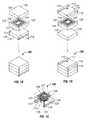
- FIGS. 1 a - 1 cseveral views of a first illustrative embodiment of a magnetic component or device 100 are shown.
- FIG. 1 aillustrates a perspective view and an exploded view of the top side of a miniature power inductor having a winding in a first winding configuration, at least one magnetic powder sheet and a vertically oriented core area in accordance with an exemplary embodiment.
- FIG. 1 billustrates a perspective view and an exploded view of the bottom side of the miniature power inductor as depicted in FIG. 1 a in accordance with an exemplary embodiment.
- FIG. 1 cillustrates a perspective view of the first winding configuration of the miniature power inductor as depicted in FIG. 1 a and FIG. 1 b in accordance with an exemplary embodiment.
- the miniature power inductor 100comprises at least one magnetic powder sheet 110 , 120 , 130 and a winding 140 coupled to the at least one magnetic powder sheet 110 , 120 , 130 in a first winding configuration 150 .
- the miniature power inductor 100comprises a first magnetic powder sheet 110 having a lower surface 112 and an upper surface 114 , a second magnetic powder sheet 120 having a lower surface 122 and an upper surface 124 , and a third magnetic powder sheet 130 having a lower surface 132 and an upper surface 134 .
- each magnetic powder sheetcan be a magnetic powder sheet manufactured by Chang Sung Incorporated in Incheon, Korea and sold under product number 20u-eff Flexible Magnetic Sheet.
- these magnetic powder sheetshave grains which are dominantly oriented in a particular direction. Thus, a higher inductance may be achieved when the magnetic field is created in the direction of the dominant grain orientation.
- this embodimentdepicts three magnetic powder sheets, the number of magnetic sheets may be increased or reduced so as to increase or decrease the number of turns in the winding or to increase or decrease the core area without departing from the scope and spirit of the exemplary embodiment.
- this embodimentdepicts a magnetic powder sheet, any flexible sheet may be used that is capable of being laminated, without departing from the scope and spirit of the exemplary embodiment.
- the first magnetic powder sheet 110also includes a first terminal 116 and a second terminal 118 coupled to opposing longitudinal edges of the lower surface 112 of the first magnetic powder sheet 110 .
- These terminals 116 , 118may be used to couple the miniature power inductor 100 to an electrical circuit, which may be on a printed circuit board (not shown), for example.
- Each of the terminals 116 , 118also comprises a via 117 , 119 for coupling the terminals 116 , 118 to one or more winding layers, which will be further discussed below.
- the vias 117 , 119are conductive connectors which proceed from the terminals 116 , 118 on the lower surface 112 to the upper surface 114 of the first magnetic powder sheet 110 .
- the viasmay be formed by drilling a hole through the magnetic powder sheets and plating the inner circumference of the drilled hole with conductive material. Alternatively, a conductive pin may be placed into the drilled holes to establish the conductive connections in the vias.
- the vias 117 , 119are shown to be cylindrical in shape, the vias may be a different geometric shape, for example, rectangular, without departing from the scope and spirit of the exemplary embodiment. In one exemplary embodiment, the entire inductor can be formed and pressed before drilling the vias.
- the terminalsare shown to be coupled to opposing longitudinal edges, the terminals may be coupled at alternative locations on the lower surface of the first magnetic powder sheet without departing from the scope and spirit of the exemplary embodiment.
- each terminalis shown to have one via, additional vias may be formed in each of the terminals so as to position the one or more winding layers in parallel, rather than in series, depending upon the application, without departing from the scope and spirit of the exemplary embodiment.
- the second magnetic powder sheet 120has a first winding layer 126 coupled to the lower surface 122 and a second winding layer 128 coupled to the upper surface 124 of the second magnetic powder sheet 120 . Both winding layers 126 , 128 combine to form the winding 140 .
- the first winding layer 126is coupled to the terminal 116 through the via 117 .
- the second winding layer 128is coupled to the first winding layer 126 through via 127 , which is formed in the second magnetic powder sheet 120 . Via 127 proceeds from the lower surface 122 to the upper surface 124 of the second magnetic powder sheet 120 .
- the second winding layer 128is coupled to the second terminal 118 through vias 129 , 119 .
- Via 129proceeds from the upper surface 124 to the lower surface 122 of the second magnetic powder sheet 120 .
- two winding layersare shown to be coupled to the second magnetic powder sheet in this embodiment, there may be one winding layer coupled to the second magnetic powder sheet without departing from the scope and spirit of the exemplary embodiment.
- the winding layers 126 , 128are formed from a conductive copper layer which is coupled to the second magnetic powder sheet 120 .
- This conductive copper layermay include, but is not limited to, a stamped copper foil, an etched copper trace, or a preformed coil without departing from the scope and spirit of the exemplary embodiment.
- the etched copper tracemay be formed, but is not limited to, chemical processes, photolithography techniques, or by laser etching techniques.
- the winding layeris a rectangular-shaped spiral pattern. However, other patterns may be used to form the winding without departing from the scope and spirit of the exemplary embodiment.
- copperis used as the conductive material, other conductive materials may be used without departing from the scope and spirit of the exemplary embodiment.
- the terminals 116 , 118may also be formed using a stamped copper foil, an etched copper trace, or by any other suitable method.
- the third magnetic powder sheet 130is placed on the upper surface 124 of the second magnetic powder sheet 120 so that the second winding layer 128 may be insulated and also so that the core area may be increased for handling higher current flow.
- the third magnetic powder sheetis not shown to have a winding layer, a winding layer may be added to the lower surface of the third magnetic layer in lieu of the winding layer on the upper surface of the second magnetic powder sheet without departing from the scope and spirit of the exemplary embodiment. Additionally, although the third magnetic powder sheet is not shown to have a winding layer, a winding layer may be added to the upper surface of the third magnetic layer without departing from the scope and spirit of the exemplary embodiment.
- the sheets 110 , 120 , 130are pressed with high pressure, for example, hydraulic pressure, and laminated together to form the miniature power inductor 100 .
- high pressurefor example, hydraulic pressure
- the viasare formed, as previously discussed.
- the physical gap between the winding and the corewhich is typically found in conventional inductors, is removed. The elimination of this physical gap tends to minimize the audible noise from the vibration of the winding.
- the miniature power inductor 100is depicted as a cube shape. However, other geometrical shapes, including but not limited to rectangular, circular, or elliptical shapes, may be used without departing from the scope and spirit of the exemplary embodiment.
- the winding 140includes a first winding layer 126 and a second winding layer 128 and forms a first winding configuration 150 having a vertically oriented core 157 .
- the first winding configuration 150starts at the first terminal 116 , then proceeds to the first winding layer 126 , then proceeds to the second winding layer 128 , and then proceeds to the second terminal 118 .
- the magnetic fieldmay be created in a direction that is perpendicular to the direction of grain orientation and thereby achieve a lower inductance or the magnetic field may be created in a direction that is parallel to the direction of grain orientation and thereby achieve a higher inductance depending upon which direction the magnetic powder sheet is extruded.
- FIGS. 2 a - 2 cseveral views of a second illustrative embodiment of a magnetic component or device 200 are shown.
- FIG. 2 aillustrates a perspective view and an exploded view of the top side of a miniature power inductor having a winding in a second winding configuration, at least one magnetic powder sheet and a horizontally oriented core area in accordance with an exemplary embodiment.
- FIG. 2 billustrates a perspective view and an exploded view of the bottom side of the miniature power inductor as depicted in FIG. 2 a in accordance with an exemplary embodiment.
- FIG. 2 cillustrates a perspective view of the second winding configuration of the miniature power inductor as depicted in FIG. 2 a and FIG. 2 b in accordance with an exemplary embodiment.
- the miniature power inductor 200comprises at least one magnetic powder sheet 210 , 220 , 230 , 240 and a winding 250 coupled to the at least one magnetic powder sheet 210 , 220 , 230 , 240 in a second winding configuration 255 .
- the miniature power inductor 200comprises a first magnetic powder sheet 210 having a lower surface 212 and an upper surface 214 , a second magnetic powder sheet 220 having a lower surface 222 and an upper surface 224 , a third magnetic powder sheet 230 having a lower surface 232 and an upper surface 234 , and a fourth magnetic powder sheet 240 having a lower surface 242 and an upper surface 244 .
- the exemplary magnetic powder sheetscan be magnetic powder sheets manufactured by Chang Sung Incorporated in Incheon, Korea and sold under product number 20u-eff Flexible Magnetic Sheet, and have the same characteristics as described above.
- this embodimentdepicts four magnetic powder sheets, the number of magnetic sheets may be increased or reduced so as to increase or decrease the core area without departing from the scope and spirit of the exemplary embodiment.
- this embodimentdepicts a magnetic powder sheet, any flexible sheet may be used that is capable of being laminated, without departing from the scope and spirit of the exemplary embodiment.
- the first magnetic powder sheet 210also includes a first terminal 216 and a second terminal 218 coupled to opposing longitudinal sides of the lower surface 212 of the first magnetic powder sheet 210 . These terminals 216 , 218 may be used to couple the miniature power inductor 200 to an electrical circuit, which may be on a printed circuit board (not shown), for example.
- the first magnetic powder sheet 210also includes a first bottom winding layer portion 260 , a second bottom winding layer portion 261 , a third bottom winding layer portion 262 , a fourth bottom winding layer portion 263 , and a fifth bottom winding layer portion 264 that are all positioned in substantially the same direction as the terminals 216 , 218 and positioned between the terminals 216 , 218 in a non-contacting relationship to one another.
- These bottom winding layer portions 260 , 261 , 262 , 263 , 264are also located on the lower surface 212 of the first magnetic powder sheet 210 .
- Each of the terminals 216 , 218comprises a via 280 , 295 , respectively, for coupling the terminals 216 , 218 to one or more winding layers.
- each of the bottom winding layer portions 260 , 261 , 262 , 263 , 264comprise two vias for coupling the bottom winding layer portions 260 , 261 , 262 , 263 , 264 to a respective top winding layer portions 270 , 271 , 272 , 273 , 274 , 275 , which is described in detail below. As listed, there is one additional top winding layer portion than bottom winding layer portion.
- the second magnetic powder sheet 220 and the third magnetic powder sheet 230comprise a plurality of vias 280 , 281 , 282 , 283 , 284 , 285 , 290 , 291 , 292 , 293 , 294 , 295 for coupling the terminals 216 , 218 , the bottom winding layer portions 260 , 261 , 262 , 263 , 264 , and top winding layer portions 270 , 271 , 272 , 273 , 274 , 275 to one another.
- the fourth magnetic powder sheet 240also includes a first top winding layer portion 270 , a second top winding layer portion 271 , a third top winding layer portion 272 , a fourth top winding layer portion 273 , a fifth top winding layer portion 274 , and a sixth top winding layer portion 275 that are positioned in substantially the same direction as the bottom winding layer portions 260 , 261 , 262 , 263 , 264 of the first magnetic powder sheet 210 .
- These top winding layer portions 270 , 271 , 272 , 273 , 274 , 275are positioned in a non-contacting relationship to one another.
- top winding layer portions 270 , 271 , 272 , 273 , 274 , 275are also located on the upper surface 244 of the fourth magnetic powder sheet 240 . Although the top winding layer portions 270 , 271 , 272 , 273 , 274 , 275 are positioned in substantially the same direction as the bottom layer winding portions 260 , 261 , 262 , 263 , 264 , there is a small angle formed between their directions so that they may be properly connected to one another.
- Each of the top winding layer portions 270 , 271 , 272 , 273 , 274 , 275comprise two vias for coupling the top winding layer portions 270 , 271 , 272 , 273 , 274 , 275 to a respective bottom winding layer portions 260 , 261 , 262 , 263 , 264 , and to a respective terminal 216 , 218 , which is described in detail below.
- the top winding layer portions 270 , 271 , 272 , 273 , 274 , 275 , the bottom winding layer portions 260 , 261 , 262 , 263 , 264 , and the terminals 216 , 218may be formed by any of the methods described above, which includes, but is not limited to, a stamped copper foil, an etched copper trace, or a preformed coil.
- the second magnetic sheet 220 and the third magnetic sheet 230are placed between the first magnetic powder sheet 210 and the fourth magnetic powder sheet 240 .
- the magnetic powder sheets 210 , 220 , 230 , 240are then pressed together with high pressure, for example, hydraulic pressure, and laminated together to form the miniature power inductor 200 .
- the vias 280 , 281 , 282 , 283 , 284 , 285 , 290 , 291 , 292 , 293 , 294 , 295are formed, in accordance to the description provided for FIGS.
- a coating or epoxymay be applied as an insulator layer to the upper surface 244 of the fourth magnetic powder sheet 240 .
- the physical gap between the winding and the corewhich is typically found in conventional inductors, is removed. The elimination of this physical gap tends to minimize the audible noise from the vibration of the winding.
- the winding 250forms a second winding configuration 255 having a horizontally oriented core 257 .
- the second winding configuration 255starts at the first terminal 216 , then proceeds to the first top winding layer portion 270 through via 280 , then proceeds to the first bottom winding layer portion 260 through via 290 , then proceeds to the second top winding layer portion 271 through via 281 , then proceeds to the second bottom winding layer portion 261 through via 291 , then proceeds to the third top winding layer portion 272 through via 282 , then proceeds to the third bottom winding layer portion 262 through via 292 , then proceeds to the fourth top winding layer portion 273 through via 283 , then proceeds to the fourth bottom winding layer portion 263 through via 293 , then proceeds to the fifth top winding layer portion 274 through via 284 , then proceeds to the fifth bottom winding layer portion 264 through via 294 , then proceeds to the sixth top winding layer portion 275 through via 285 , then proceeds to the second terminal 218 through via 295
- the magnetic fieldmay be created in a direction that is perpendicular to the direction of grain orientation and thereby achieve a lower inductance or the magnetic field may be created in a direction that is parallel to the direction of grain orientation and thereby achieve a higher inductance depending upon which direction the magnetic powder sheet is extruded.
- the miniature power inductor 200is depicted as square shape. However, other geometrical shapes, including but not limited to rectangular, circular, or elliptical shapes, may be used without departing from the scope and spirit of the exemplary embodiment. Also, although this embodiment depicts six top winding layer portions and five bottom winding layer portions, the number of top and bottom winding layer portions may increase or decrease depending upon application requirements, so long as that there is one more top winding layer portion than bottom winding layer portion, without departing from the scope and spirit of the exemplary embodiment.
- FIGS. 3 a - 3 cseveral views of a third illustrative embodiment of a magnetic component or device 300 are shown.
- FIG. 3 aillustrates a perspective view and an exploded view of the top side of a miniature power inductor having a portion of a winding in the second winding configuration and at least one terminal located on a printed circuit board, at least one magnetic powder sheet and a horizontally oriented core area in accordance with an exemplary embodiment.
- FIG. 3 billustrates a perspective view and an exploded view of the bottom side of the miniature power inductor as depicted in FIG. 3 a in accordance with an exemplary embodiment.
- FIG. 3 cillustrates a perspective view of the second winding configuration of the miniature power inductor as depicted in FIG. 3 a and FIG. 3 b in accordance with an exemplary embodiment.
- the miniature power inductor 300 shown in FIGS. 3 a - 3 cis similar to the miniature power inductor 200 shown in FIGS. 2 a - 2 c except that a first terminal 316 , a second terminal 318 , and a plurality of bottom winding layer portions 360 , 361 , 362 , 363 , 364 are now located on the upper surface 304 of a substrate 302 , instead of on the lower surface 312 of a first magnetic powder sheet 310 .
- a first terminal 316 , a second terminal 318 , and a plurality of bottom winding layer portions 360 , 361 , 362 , 363 , 364are now located on the upper surface 304 of a substrate 302 , instead of on the lower surface 312 of a first magnetic powder sheet 310 .
- the first magnetic powder sheet 310is utilized in the manufacturing of the miniature power inductor 300 and comprises a plurality of vias, similar to a second magnetic powder sheet 320 and a third magnetic powder sheet 330 .
- the miniature power inductor 300is not completely formed until it is coupled to the substrate 302 having the proper terminals 316 , 318 and the plurality of bottom winding layer portions 360 , 361 , 362 , 363 , 364 .
- the pressed magnetic powder sheets 310 , 320 , 330 , 340may be coupled to the substrate 302 in any known manner, including but not limited to soldering of each of the vias to the substrate 302 .
- the substrate 302may include, but is not limited to, a printed circuit board and/or other substrates that are capable of having terminals and the plurality of bottom winding layer portions formed thereon.
- the manufacturing of the miniature power inductor 300will have most, if not all, of the flexibilities of the miniature power inductor 200 , as illustrated and described with respect to FIGS. 2 a - 2 c.
- FIGS. 4 a - 4 cseveral views of a fourth illustrative embodiment of a magnetic component or device 400 are shown.
- FIG. 4 aillustrates a perspective view and an exploded view of the top side of a miniature power inductor having a plurality of windings in a third winding configuration, at least one magnetic powder sheet and a horizontally oriented core area in accordance with an exemplary embodiment.
- FIG. 4 billustrates a perspective view and an exploded view of the bottom side of the miniature power inductor as depicted in FIG. 4 a in accordance with an exemplary embodiment.
- FIG. 4 cillustrates a perspective view of the third winding configuration of the miniature power inductor as depicted in FIG. 4 a and FIG. 4 b in accordance with an exemplary embodiment.
- the miniature power inductor 400comprises at least one magnetic powder sheet 410 , 420 , 430 , 440 and a plurality of windings 450 , 451 , 452 coupled to the at least one magnetic powder sheet 410 , 420 , 430 , 440 in a third winding configuration 455 .
- the miniature power inductor 400comprises a first magnetic powder sheet 410 having a lower surface 412 and an upper surface 414 , a second magnetic powder sheet 420 having a lower surface 422 and an upper surface 424 , a third magnetic powder sheet 430 having a lower surface 432 and an upper surface 434 , and a fourth magnetic powder sheet 440 having a lower surface 442 and an upper surface 444 .
- the exemplary magnetic powder sheetscan be magnetic powder sheets manufactured by Chang Sung Incorporated in Incheon, Korea and sold under product number 20u-eff Flexible Magnetic Sheet, and have the same characteristics as described above.
- this embodimentdepicts four magnetic powder sheets, the number of magnetic sheets may be increased or reduced so as to increase or decrease the core area without departing from the scope and spirit of the exemplary embodiment. Also, although this embodiment depicts a magnetic powder sheet, any flexible sheet may be used that is capable of being laminated, without departing from the scope and spirit of the exemplary embodiment.
- the first magnetic powder sheet 410also includes a first terminal 411 , a second terminal 413 , a third terminal 415 , a fourth terminal 416 , a fifth terminal 417 , and a sixth terminal 418 .
- the first terminal 411 and the second terminal 413are coupled to opposing sides of the lower surface 412 of the first magnetic powder sheet 410 .
- the third terminal 415 and the fourth terminal 416are coupled to opposing sides of the lower surface 412 of the first magnetic powder sheet 410 .
- the fifth terminal 417 and the sixth terminal 418are coupled to opposing sides of the lower surface 412 of the first magnetic powder sheet 410 .
- first terminal 411 , the third terminal 415 , and the fifth terminal 417are positioned adjacent to one another and along one edge of the lower surface 412 of the first magnetic powder sheet 410
- second terminal 413 , the fourth terminal 416 , and the sixth terminal 418are positioned adjacent to one another and along the opposing edge of the lower surface 412 of the first magnetic powder sheet 410 .
- These terminals 411 , 413 , 415 , 416 , 417 , 418may be used to couple the miniature power inductor 400 to an electrical circuit, which may be on a printed circuit board (not shown), for example.
- the first magnetic powder sheet 410also includes a first bottom winding layer portion 460 , a second bottom winding layer portion 461 , and a third bottom winding layer portion 462 that are all positioned in substantially the same direction as the terminals 411 , 413 , 415 , 416 , 417 , 418 and on the lower surface 412 of the first magnetic powder sheet 410 .
- the first bottom winding layer portion 460is positioned between the first terminal 411 and the second terminal 413 and in a non-contacting relationship to one another.
- the first bottom winding layer portion 460 , the first terminal 411 , and the second terminal 413combine to form a portion of the first winding 450 .
- the second bottom winding layer portion 461is positioned between the third terminal 415 and the fourth terminal 416 and in a non-contacting relationship to one another.
- the second bottom winding layer portion 461 , the third terminal 415 , and the fourth terminal 416combine to form a portion of the second winding 451 .
- the third bottom winding layer portion 462is positioned between the fifth terminal 417 and the sixth terminal 418 and in a non-contacting relationship to one another.
- the third bottom winding layer portion 462 , the fifth terminal 417 , and the sixth terminal 418combine to form a portion of the third winding 452 .
- Each of the terminals 411 , 413 , 415 , 416 , 417 , 418comprise a via 480 , 482 , 484 , 491 , 493 , 495 , respectively for coupling the terminals 411 , 413 , 415 , 416 , 417 , 418 to one or more winding layers.
- each of the bottom winding layer portions 460 , 461 , 462comprise two vias for coupling the bottom winding layer portions 460 , 461 , 462 to a respective top winding layer portions 470 , 471 , 472 , 473 , 474 , 475 , which is described in detail below. As listed and previously mentioned, there is one additional top winding layer portion than bottom winding layer portion per winding.
- the second magnetic powder sheet 420 and the third magnetic powder sheet 430comprise a plurality of vias 480 , 481 , 482 , 483 , 484 , 485 , 490 , 491 , 492 , 493 , 494 , 495 for coupling the terminals 411 , 413 , 415 , 416 , 417 , 418 , the bottom winding layer portions 460 , 461 , 462 , and the top winding layer portions 470 , 471 , 472 , 473 , 474 , 475 to one another.
- the fourth magnetic powder sheet 440also includes a first top winding layer portion 470 , a second top winding layer portion 471 , a third top winding layer portion 472 , a fourth top winding layer portion 473 , a fifth top winding layer portion 474 , and a sixth top winding layer portion 475 that are positioned in substantially the same direction as the bottom winding layer portions 460 , 461 , 462 of the first magnetic powder sheet 410 .
- These top winding layer portions 470 , 471 , 472 , 473 , 474 , 475are positioned in a non-contacting relationship to one another.
- top winding layer portions 470 , 471 , 472 , 473 , 474 , 475are also located on the upper surface 444 of the fourth magnetic powder sheet 440 .
- the top winding layer portions 470 , 471 , 472 , 473 , 474 , 475are positioned in substantially the same direction as the bottom layer winding portions 460 , 461 , 462 , there is a small angle formed between their directions so that they may be properly connected to one another.
- Each of the top winding layer portions 470 , 471 , 472 , 473 , 474 , 475comprise two vias for coupling the top winding layer portions 470 , 471 , 472 , 473 , 474 , 475 to a respective bottom winding layer portions 460 , 461 , 462 , and to a respective terminal 411 , 413 , 415 , 416 , 417 , 418 , which is described in detail below.
- the top winding layer portions 470 , 471 , 472 , 473 , 474 , 475 , the bottom winding layer portions 460 , 461 , 462 , and the terminals 411 , 413 , 415 , 416 , 417 , 418may be formed by any of the methods described above, which includes, but is not limited to, a stamped copper foil, an etched copper trace, or a preformed coil.
- the second magnetic sheet 420 and the third magnetic sheet 430are placed between the first magnetic powder sheet 410 and the fourth magnetic powder sheet 440 .
- the magnetic powder sheets 410 , 420 , 430 , 440are then pressed together with high pressure, for example, hydraulic pressure, and laminated together to form the miniature power inductor 400 .
- the vias 480 , 481 , 482 , 483 , 484 , 485 , 490 , 491 , 492 , 493 , 494 , 495are formed, in accordance to the description provided for FIGS.
- a coating or epoxymay be applied as an insulator layer to the upper surface 444 of the fourth magnetic powder sheet 440 .
- the physical gap between the winding and the corewhich is typically found in conventional inductors, is removed. The elimination of this physical gap tends to minimize the audible noise from the vibration of the winding.
- the windings 450 , 451 , 452form a third winding configuration 455 having a horizontally oriented core 457 .
- the first winding 450starts at the first terminal 411 , then proceeds to the first top winding layer portion 470 through via 480 , then proceeds to the first bottom winding layer portion 460 through via 490 , then proceeds to the second top winding layer portion 471 through via 481 , then proceeds to the second terminal 413 through via 491 , which then completes the first winding 450 .
- the second winding 451starts at the third terminal 415 , then proceeds to the third top winding layer portion 472 through via 482 , then proceeds to the second bottom winding layer portion 461 through via 492 , then proceeds to the fourth top winding layer portion 473 through via 483 , then proceeds to the fourth terminal 416 through via 493 , which then completes the second winding 451 .
- the third winding 452starts at the fifth terminal 417 , then proceeds to the fifth top winding layer portion 474 through via 484 , then proceeds to the third bottom winding layer portion 462 through via 494 , then proceeds to the sixth top winding layer portion 475 through via 485 , then proceeds to the sixth terminal 418 through via 495 , which then completes the third winding 452 .
- windingsare depicted in this embodiment, greater or fewer windings may be formed without departing from the scope and spirit of the exemplary embodiment. Additionally, the three windings may be mounted onto a substrate (not shown) or printed circuit board in a parallel arrangement or in a series arrangement depending upon the application and requirements that are needed. This flexibility allows this miniature power inductor 400 to be utilized as an inductor or as a transformer.
- the magnetic fieldmay be created in a direction that is perpendicular to the direction of grain orientation and thereby achieve a lower inductance or the magnetic field may be created in a direction that is parallel to the direction of grain orientation and thereby achieve a higher inductance depending upon which direction the magnetic powder sheet is extruded.
- the miniature power inductor 400is depicted as square shape. However, other geometrical shapes, including but not limited to rectangular, circular, or elliptical shapes, may be used without departing from the scope and spirit of the exemplary embodiment. Also, although this embodiment depicts two top winding layer portions and one bottom winding layer portion for each winding, the number of top and bottom winding layer portions may increase depending upon application requirements, so long as that there is one more top winding layer portion than bottom winding layer portion for each winding, without departing from the scope and spirit of the exemplary embodiment.
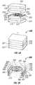
- FIGS. 5 a - 5 bseveral views of a fifth illustrative embodiment of a magnetic component or device 500 are shown.
- FIG. 5 aillustrates a perspective view and an exploded view of the top side of a miniature power inductor having a preformed coil and at least one magnetic powder sheet in accordance with an exemplary embodiment.
- FIG. 5 billustrates a perspective transparent view of the miniature power inductor as depicted in FIG. 5 a in accordance with an exemplary embodiment.
- the miniature power inductor 500comprises at least one magnetic powder sheet 510 , 520 , 530 , 540 and at least one preformed coil 550 coupled to the at least one magnetic powder sheet 510 , 520 , 530 , 540 .
- the miniature power inductor 500comprises a first magnetic powder sheet 510 having a lower surface 512 and an upper surface 514 , a second magnetic powder sheet 520 having a lower surface 522 and an upper surface 524 , a third magnetic powder sheet 530 having a lower surface 532 and an upper surface 534 , and a fourth magnetic powder sheet 540 having a lower surface 542 and an upper surface 544 .
- the exemplary magnetic powder sheetscan be magnetic powder sheets manufactured by Chang Sung Incorporated in Incheon, Korea and sold under product number 20u-eff Flexible Magnetic Sheet, and have the same characteristics as described above.
- this embodimentdepicts four magnetic powder sheets, the number of magnetic sheets may be increased or reduced so as to increase or decrease the core area without departing from the scope and spirit of the exemplary embodiment.
- this embodimentdepicts a magnetic powder sheet, any flexible sheet may be used that is capable of being laminated, without departing from the scope and spirit of the exemplary embodiment.
- this embodimentdepicts the use of one preformed coil
- additional preformed coilsmay be used with the addition of more magnetic powder sheets by altering one or more of the terminations so that the more than one preformed coils may be positioned in parallel or in series, without departing from the scope and spirit of the exemplary embodiment.
- the first magnetic powder sheet 510also includes a first terminal 516 and a second terminal 518 coupled to opposing longitudinal sides of the lower surface 512 of the first magnetic powder sheet 510 .
- the terminals 516 , 518extend the entire length of the longitudinal side.
- this embodimentdepicts the terminals extending along the entire opposing longitudinal sides, the terminals may extend only a portion of the opposing longitudinal sides without departing from the scope and spirit of the exemplary embodiment.
- these terminals 516 , 518may be used to couple the miniature power inductor 500 to an electrical circuit, which may be on a printed circuit board (not shown), for example.
- the second magnetic powder sheet 520also includes a third terminal 526 and a fourth terminal 528 coupled to opposing longitudinal sides of the lower surface 522 of the second magnetic powder sheet 520 .
- the terminals 526 , 528extend the entire length of the longitudinal side, similar to the terminals 516 , 518 of the first magnetic powder sheet 510 .
- this embodimentdepicts the terminals extending along the entire opposing longitudinal sides, the terminals may extend only a portion of the opposing longitudinal sides without departing from the scope and spirit of the exemplary embodiment. Additionally, these terminals 526 , 528 may be used to couple the first terminal 516 and the second terminal 518 to the at least one preformed coil 550 .
- the terminals 516 , 518 , 526 , 528may be formed by any of the methods described above, which includes, but is not limited to, a stamped copper foil or etched copper trace.
- Each of the first magnetic powder sheet 510 and the second magnetic powder sheet 520further include a plurality of vias 580 , 581 , 582 , 583 , 584 , 590 , 591 , 592 , 593 , 594 extending from the upper surface 524 of the second magnetic powder sheet 520 to the lower surface 512 of the first magnetic powder sheet 510 .
- these plurality of vias 580 , 581 , 582 , 583 , 584 , 590 , 591 , 592 , 593 , 594are positioned on the terminals 516 , 518 , 526 , 528 in a substantially linear pattern.
- first magnetic powder sheet 510 and the second magnetic powder sheet 520There are five vias positioned along one of the edges of the first magnetic powder sheet 510 and the second magnetic powder sheet 520 , and there are five vias positioned along the opposing edge of the first magnetic powder sheet 510 and the second magnetic powder sheet 520 . Although five vias are shown along each of the opposing longitudinal edges, there may be greater or fewer vias without departing from the scope and spirit of the exemplary embodiment. Additionally, although vias are used to couple first and second terminals 516 , 518 to third and fourth terminals 526 , 528 , alternative coupling may be used without departing from the scope and spirit of the exemplary embodiment.
- One such alternative couplingincludes, but is not limited to, metal plating along at least a portion of the opposing side faces 517 , 519 , 527 , 529 of both first magnetic powder sheet 510 and second magnetic powder sheet 520 and extending from the first and second terminals 516 , 518 to the third and fourth terminals 526 , 528 .
- the alternative couplingmay include metal plating that extends the entire opposing side faces 517 , 519 , 527 , 529 and also wraps around the opposing side faces 517 , 519 , 527 , 529 .
- alternative couplingsuch as the metal plating of the opposing side faces
- the viasmay be used in addition to or in lieu of the alternative coupling, such as metal plating of the opposing side faces.
- the first magnetic powder sheet 510 and the second magnetic powder sheet 520are pressed together with high pressure, for example, hydraulic pressure, and laminated together to form a portion of the miniature power inductor 500 .
- the vias 580 , 581 , 582 , 583 , 584 , 590 , 591 , 592 , 593 , 594are formed, in accordance to the description provided for FIGS. 1 a - 1 c .
- other terminationsmay be made between the two sheets 510 , 520 without departing from the scope and spirit of the exemplary embodiment.
- a preformed winding or coil 550 having a first lead 552 and a second lead 554may be positioned on the upper surface 524 of the second magnetic powder sheet 520 , where the first lead 552 is coupled to either the third terminal 526 or the fourth terminal 528 and the second lead is coupled to the other terminal 526 , 528 .
- the preformed winding 550may be coupled to the terminals 526 , 528 via welding or other known coupling methods.
- the third magnetic powder sheet 530 and the fourth magnetic powder sheet 540may then be pressed together along with the previously pressed portion of the miniature power inductor 500 to form the completed miniature power inductor 500 .
- the physical gap between the winding and the corewhich is typically found in conventional inductors, is removed. The elimination of this physical gap tends to minimize the audible noise from the vibration of the winding.
- magnetic sheetsmay positioned between the first and second magnetic powder sheets so long as there remains an electrical connection between the terminals of the first and second magnetic powder sheets without departing from the scope and spirit of the exemplary embodiment. Additionally, although two magnetic powder sheets are shown to be positioned above the preformed coil, greater or fewer sheets may be used to increase or decrease the core area without departing from the scope and spirit of the exemplary embodiment.
- the magnetic fieldmay be created in a direction that is perpendicular to the direction of grain orientation and thereby achieve a lower inductance or the magnetic field may be created in a direction that is parallel to the direction of grain orientation and thereby achieve a higher inductance depending upon which direction the magnetic powder sheet is extruded.
- the miniature power inductor 500is depicted as a rectangular shape. However, other geometrical shapes, including but not limited to square, circular, or elliptical shapes, may be used without departing from the scope and spirit of the exemplary embodiment.
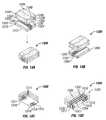
- FIGS. 6 a - 6 cseveral views of a sixth illustrative embodiment of a magnetic component or device 600 are shown.
- FIG. 6 aillustrates a perspective view and an exploded view of the top side of a miniature power inductor having a plurality of windings in a fourth winding configuration, at least one magnetic powder sheet, and a plurality of horizontally oriented core areas in accordance with an exemplary embodiment.
- FIG. 6 billustrates a perspective view and an exploded view of the bottom side of the miniature power inductor as depicted in FIG. 6 a in accordance with an exemplary embodiment.
- FIG. 6 cillustrates a perspective view of the fourth winding configuration of the miniature power inductor as depicted in FIG. 6 a and FIG. 6 b in accordance with an exemplary embodiment.
- the miniature power inductor 600comprises at least one magnetic powder sheet 610 , 620 , 630 , 640 and a plurality of windings 650 , 651 , 652 coupled to the at least one magnetic powder sheet 610 , 620 , 630 , 640 in a fourth winding configuration 655 .
- the miniature power inductor 600comprises a first magnetic powder sheet 610 having a lower surface 612 and an upper surface 614 , a second magnetic powder sheet 620 having a lower surface 622 and an upper surface 624 , a third magnetic powder sheet 630 having a lower surface 632 and an upper surface 634 , and a fourth magnetic powder sheet 640 having a lower surface 642 and an upper surface 644 .
- the exemplary magnetic powder sheetscan be magnetic powder sheets manufactured by Chang Sung Incorporated in Incheon, Korea and sold under product number 20u-eff Flexible Magnetic Sheet, and have the same characteristics as described above.
- this embodimentdepicts four magnetic powder sheets, the number of magnetic sheets may be increased or reduced so as to increase or decrease the core area without departing from the scope and spirit of the exemplary embodiment. Also, although this embodiment depicts a magnetic powder sheet, any suitable flexible sheet may be used that is capable of being laminated, without departing from the scope and spirit of the exemplary embodiment.
- the first magnetic powder sheet 610also includes a first terminal 611 , a second terminal 613 , a third terminal 615 , a fourth terminal 616 , a fifth terminal 617 , and a sixth terminal 618 .
- the first terminal 611 and the second terminal 613are coupled to opposing sides of the lower surface 612 of the first magnetic powder sheet 610 .
- the third terminal 615 and the fourth terminal 616are coupled to opposing sides of the lower surface 612 of the first magnetic powder sheet 610 .
- the fifth terminal 617 and the sixth terminal 618are coupled to opposing sides of the lower surface 612 of the first magnetic powder sheet 610 .
- first terminal 611 , the third terminal 615 , and the fifth terminal 617are positioned adjacent to one another and along one edge of the lower surface 612 of the first magnetic powder sheet 610
- second terminal 613 , the fourth terminal 616 , and the sixth terminal 618are positioned adjacent to one another and along the opposing edge of the lower surface 612 of the first magnetic powder sheet 610 .
- These terminals 611 , 613 , 615 , 616 , 617 , 618may be used to couple the miniature power inductor 600 to an electrical circuit, which may be on a printed circuit board (not shown), for example.
- the first magnetic powder sheet 610also includes a first bottom winding layer portion 660 , a second bottom winding layer portion 661 , a third bottom winding layer portion 662 , a fourth bottom winding layer portion 663 , a fifth bottom winding layer portion 664 , and a sixth bottom winding layer portion 665 that are all positioned in substantially the same direction as the terminals 611 , 613 , 615 , 616 , 617 , 618 and on the lower surface 612 of the first magnetic powder sheet 610 .
- the first bottom winding layer portion 660 and the second bottom winding layer portion 661are positioned between the first terminal 611 and the second terminal 613 and in a non-contacting relationship to one another.
- the first terminal 611 , the first bottom winding layer portion 660 , the second bottom winding layer portion 661 , and the second terminal 613are positioned in a substantially linear pattern and in that order.
- the first terminal 611 , the first bottom winding layer portion 660 , the second bottom winding layer portion 661 , and the second terminal 613combine to form a portion of the first winding 650 .
- the third bottom winding layer portion 662 and the fourth bottom winding layer portion 663are positioned between the third terminal 615 and the fourth terminal 616 and in a non-contacting relationship to one another.
- the third terminal 615 , the third bottom winding layer portion 662 , the fourth bottom winding layer portion 663 , and the fourth terminal 616are positioned in a substantially linear pattern and in that order.
- the third terminal 615 , the third bottom winding layer portion 662 , the fourth bottom winding layer portion 663 , and the fourth terminal 616combine to form a portion of the second winding 651 .
- the fifth bottom winding layer portion 664 and the sixth bottom winding layer portion 665are positioned between the fifth terminal 617 and the sixth terminal 618 and in a non-contacting relationship to one another.
- the fifth terminal 617 , the fifth bottom winding layer portion 664 , the sixth bottom winding layer portion 665 , and the sixth terminal 618are positioned in a substantially linear pattern and in that order.
- the fifth terminal 617 , the fifth bottom winding layer portion 664 , the sixth bottom winding layer portion 665 , and the sixth terminal 618combine to form a portion of the third winding 652 .
- Each of the terminals 611 , 613 , 615 , 616 , 617 , 618comprise a via 680 , 685 , 686 , 691 , 692 , 697 , respectively for coupling the terminals 611 , 613 , 615 , 616 , 617 , 618 to one or more winding layers.
- each of the bottom winding layer portions 660 , 661 , 662 , 663 , 664 , 665comprise two vias for coupling the bottom winding layer portions 660 , 661 , 662 , 663 , 664 , 665 to a top winding layer portion 670 , 671 , 672 , 673 , 674 , 675 , 676 , 677 , 678 which is described in detail below. As listed and previously mentioned, there is one additional top winding layer portion than bottom winding layer portion per winding.
- the viasare shown to be rectangular, other geometric shapes, including but not limited to circular shapes, may be used without departing from the scope and spirit of the exemplary embodiment.
- the second magnetic powder sheet 620 and the third magnetic powder sheet 630comprise a plurality of vias 680 , 681 , 682 , 683 , 684 , 685 , 686 , 687 , 688 , 689 , 690 , 691 , 692 , 693 , 694 , 695 , 696 , 697 for coupling the terminals 611 , 613 , 615 , 616 , 617 , 618 , the bottom winding layer portions 660 , 661 , 662 , 663 , 664 , 665 , and the top winding layer portions 670 , 671 , 672 , 673 , 674 , 675 , 676 , 677 , 678 to one another.
- the fourth magnetic powder sheet 640also includes a first top winding layer portion 670 , a second top winding layer portion 671 , a third top winding layer portion 672 , a fourth top winding layer portion 673 , a fifth top winding layer portion 674 , a sixth top winding layer portion 675 , a seventh top winding layer portion 676 , an eighth top winding layer portion 677 , and a ninth top winding layer portion 678 that are positioned in substantially the same direction as the bottom winding layer portions 660 , 661 , 662 , 663 , 664 , 665 of the first magnetic powder sheet 610 .
- top winding layer portions 670 , 671 , 672 , 673 , 674 , 675 , 676 , 677 , 678are positioned in a non-contacting relationship to one another. These top winding layer portions 670 , 671 , 672 , 673 , 674 , 675 , 676 , 677 , 678 are also located on the upper surface 644 of the fourth magnetic powder sheet 640 .
- the first top winding layer portion 670 , the second top winding layer portion 671 , and the third top winding layer portion 672are positioned overlying the gaps formed between the first terminal 611 , the first bottom winding layer portion 660 , the second bottom winding layer portion 661 , and the second terminal 613 of the first magnetic powder sheet 610 and in an overlapping relationship. Additionally, the fourth top winding layer portion 673 , the fifth top winding layer portion 674 , and the sixth top winding layer portion 675 are positioned overlying the gaps formed between the third terminal 615 , the third bottom winding layer portion 662 , the fourth bottom winding layer portion 663 , and the fourth terminal 616 of the first magnetic powder sheet 610 and in an overlapping relationship.
- the seventh top winding layer portion 676 , the eighth top winding layer portion 677 , and the ninth top winding layer portion 678are positioned overlying the gaps formed between the fifth terminal 617 , the fifth bottom winding layer portion 664 , the sixth bottom winding layer portion 665 , and the sixth terminal 618 of the first magnetic powder sheet 610 and in an overlapping relationship.
- Each of the top winding layer portions 670 , 671 , 672 , 673 , 674 , 675 , 676 , 677 , 678comprise two vias for coupling the top winding layer portions 670 , 671 , 672 , 673 , 674 , 675 , 676 , 677 , 678 to a respective bottom winding layer portions 660 , 661 , 662 , 663 , 664 , 665 , and to a respective terminal 611 , 613 , 615 , 616 , 617 , 618 , which is described in detail below.
- the top winding layer portions 670 , 671 , 672 , 673 , 674 , 675 , 676 , 677 , 678 , the bottom winding layer portions 670 , 671 , 672 , 673 , 674 , 675 , 676 , 677 , 678 , and the terminals 611 , 613 , 615 , 616 , 617 , 618may be formed by any of the methods described above, which includes, but is not limited to, a stamped copper foil, an etched copper trace, or a preformed coil.
- the second magnetic sheet 620 and the third magnetic sheet 630are placed between the first magnetic powder sheet 610 and the fourth magnetic powder sheet 640 .
- the magnetic powder sheets 610 , 620 , 630 , 640are then pressed together with high pressure, for example, hydraulic pressure, and laminated together to form the miniature power inductor 600 .
- the vias 680 , 681 , 682 , 683 , 684 , 685 , 686 , 687 , 688 , 689 , 690 , 691 , 692 , 693 , 694 , 695 , 696 , 697are formed, in accordance to the description provided for FIGS. 1 a - 1 c .
- a coating or epoxy(not shown) may be applied as an insulator layer to the upper surface 644 of the fourth magnetic powder sheet 640 .
- the physical gap between the winding and the corewhich is typically found in conventional inductors, is removed. The elimination of this physical gap tends to minimize the audible noise from the vibration of the winding.
- the windings 650 , 651 , 652form a fourth winding configuration 655 having a plurality of horizontally oriented cores 657 , 658 , 659 .
- the first winding 650starts at the first terminal 611 , then proceeds to the first top winding layer portion 670 through via 680 , then proceeds to the first bottom winding layer portion 660 through via 681 , then proceeds to the second top winding layer portion 671 through via 682 , then proceeds to the second bottom winding layer portion 661 through via 683 , then proceeds to the third top winding layer 672 through via 684 , and then proceeds to the second terminal 613 through via 685 , which then completes the first winding 650 .
- the second winding 651starts at the third terminal 615 , then proceeds to the fourth top winding layer portion 673 through via 686 , then proceeds to the third bottom winding layer portion 662 through via 687 , then proceeds to the fifth top winding layer portion 674 through via 688 , then proceeds to the fourth bottom winding layer portion 663 through via 689 , then proceeds to the sixth top winding layer 675 through via 690 , and then proceeds to the fourth terminal 616 through via 691 , which then completes the second winding 651 .
- the third winding 652starts at the fifth terminal 617 , then proceeds to the seventh top winding layer portion 676 through via 692 , then proceeds to the fifth bottom winding layer portion 664 through via 693 , then proceeds to the eighth top winding layer portion 677 through via 694 , then proceeds to the sixth bottom winding layer portion 665 through via 695 , then proceeds to the ninth top winding layer 678 through via 696 , and then proceeds to the sixth terminal 618 through via 697 , which then completes the second winding 652 .
- the three windingsmay be mounted onto a substrate (not shown) or printed circuit board in a parallel arrangement or in a series arrangement depending upon the application and requirements that are needed. This flexibility allows this miniature power inductor 600 to be utilized as an inductor, a multi-phase inductor, or as a transformer.
- the magnetic fieldmay be created in a direction that is perpendicular to the direction of grain orientation and thereby achieve a lower inductance or the magnetic field may be created in a direction that is parallel to the direction of grain orientation and thereby achieve a higher inductance depending upon which direction the magnetic powder sheet is extruded.
- the miniature power inductor 600is depicted as a rectangular shape. However, other geometrical shapes, including but not limited to square, circular, or elliptical shapes, may be used without departing from the scope and spirit of the exemplary embodiment. Also, although this embodiment depicts three top winding layer portions and two bottom winding layer portion for each winding, the number of top and bottom winding layer portions may increase or decrease depending upon application requirements, so long as that there is one more top winding layer portion than bottom winding layer portion for each winding, without departing from the scope and spirit of the exemplary embodiment.
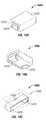
- FIGS. 7 a - 7 cseveral views of a seventh illustrative embodiment of a magnetic component or device 700 are shown.
- FIG. 7 aillustrates a perspective view and an exploded view of the top side of a miniature power inductor having a winding in a fifth winding configuration, at least one magnetic powder sheet, and a plurality of horizontally oriented core areas in accordance with an exemplary embodiment.
- FIG. 7 billustrates a perspective view and an exploded view of the bottom side of the miniature power inductor as depicted in FIG. 7 a in accordance with an exemplary embodiment.
- FIG. 7 cillustrates a perspective view of the fifth winding configuration of the miniature power inductor as depicted in FIG. 7 a and FIG. 7 b in accordance with an exemplary embodiment.
- the miniature power inductor 700 shown in FIGS. 7 a - 7 cis similar to the miniature power inductor 600 shown in FIGS. 6 a - 6 c except that the three windings 650 , 651 , 652 shown in FIGS. 6 a - 6 c are now a single winding 750 as shown in FIGS. 7 a - 7 c .
- This modificationmay occur by replacing the second terminal 613 and the fourth terminal 616 of the first magnetic powder sheet 610 with a seventh bottom winding layer portion 766 that is oriented substantially perpendicular to the remaining bottom winding layers 760 , 761 , 762 , 763 , 764 , 765 .
- the seventh bottom winding layer portion 766may be a length sufficient to overlap the width of two bottom winding layer portions and the gap formed between the two adjacent bottom winding layer portions. Additionally, the third terminal 615 and the fifth terminal 617 of the first magnetic powder sheet 610 (as shown in FIGS. 6 a - 6 c ) may be replaced with an eighth bottom winding layer portion 767 that is oriented substantially perpendicular to the remaining bottom winding layers 760 , 761 , 762 , 763 , 764 , 765 . The eighth bottom winding layer portion 767 also may be a length sufficient to overlap the width of two bottom winding layer portions and the gap formed between the two adjacent bottom winding layer portions. With these modifications, the multi-phase inductor of FIGS. 6 a - 6 c may be transformed into a single phase inductor.
- the winding 750form a fifth winding configuration 755 having a plurality of horizontally oriented cores 757 , 758 , 759 .
- the winding 750starts at the first terminal 711 , then proceeds to the first top winding layer portion 770 through via 780 , then proceeds to the first bottom winding layer portion 760 through via 781 , then proceeds to the second top winding layer portion 771 through via 782 , then proceeds to the second bottom winding layer portion 761 through via 783 , then proceeds to the third top winding layer 772 through via 784 , then proceeds to the seventh bottom winding layer portion 766 through via 785 , then proceeds to the sixth top winding layer portion 775 through via 791 , then proceeds to the fourth bottom winding layer portion 763 through via 790 , then proceeds to the fifth top winding layer portion 774 through via 789 , then proceeds to the third bottom winding layer portion 762 through via 788 , then proceeds to the fourth top winding layer 773 through via 787 , then proceeds to the
- the manufacturing of the miniature power inductor 700will have most, if not all, of the flexibilities of the miniature power inductor 600 , as illustrated and described with respect to FIGS. 6 a - 6 c.
- FIGS. 8 a - 8 cseveral views of an eighth illustrative embodiment of a magnetic component or device 800 are shown.
- FIG. 8 aillustrates a perspective view and an exploded view of the top side of a miniature power inductor having a winding in a sixth winding configuration, at least one magnetic powder sheet, and a vertically oriented core area and a circularly oriented core area in accordance with an exemplary embodiment.
- FIG. 8 billustrates a perspective view and an exploded view of the bottom side of the miniature power inductor as depicted in FIG. 8 a in accordance with an exemplary embodiment.
- FIG. 8 cillustrates a perspective view of the sixth winding configuration of the miniature power inductor as depicted in FIG. 8 a and FIG. 8 b in accordance with an exemplary embodiment;
- the miniature power inductor 800comprises at least one magnetic powder sheet 810 , 820 , 830 , 840 and a winding 850 coupled to the at least one magnetic powder sheet 810 , 820 , 830 , 840 in a sixth winding configuration 855 .
- the miniature power inductor 800comprises a first magnetic powder sheet 810 having a lower surface 812 and an upper surface 814 , a second magnetic powder sheet 820 having a lower surface 822 and an upper surface 824 , a third magnetic powder sheet 830 having a lower surface 832 and an upper surface 834 , and a fourth magnetic powder sheet 840 having a lower surface 842 and an upper surface 844 .
- the exemplary magnetic powder sheetscan be magnetic powder sheets manufactured by Chang Sung Incorporated in Incheon, Korea and sold under product number 20u-eff Flexible Magnetic Sheet, and have the same characteristics as described above.
- this embodimentdepicts four magnetic powder sheets, the number of magnetic sheets may be increased or reduced so as to increase or decrease the core area without departing from the scope and spirit of the exemplary embodiment.
- this embodimentdepicts a magnetic powder sheet, any flexible sheet may be used that is capable of being laminated, without departing from the scope and spirit of the exemplary embodiment.
- the first magnetic powder sheet 810has a first cutout 802 and a second cutout 804 positioned at adjacent corners of the first magnetic powder sheet 810 .
- the first magnetic powder sheet 810also includes a first terminal 816 extending from the first cutout 802 towards a first non-cutout corner 806 and coupled to a longitudinal side of the lower surface 812 of the first magnetic powder sheet 810 .
- the first magnetic powder sheet 810also includes a second terminal 818 extending from the second cutout 804 towards a second non-cutout corner 808 and coupled to an opposing longitudinal side of the lower surface 812 of the first magnetic powder sheet 810 .
- terminals 816 , 818may be used to couple the miniature power inductor 800 to an electrical circuit, which may be on a printed circuit board (not shown), for example.
- the first magnetic powder sheet 810also includes a plurality of bottom winding layer portions 860 that are all positioned to form a substantially circular pattern having an inner circumference 862 and an outer circumference 864 .
- the plurality of bottom winding layer portions 860extend from the inner circumference 862 to the outer circumference 864 at a slight angle from the shortest path from the inner circumference 862 to the outer circumference 864 .
- the terminals 816 , 818 and the plurality of bottom winding layer portions 860are positioned in a non-contacting relationship to one another. These plurality of bottom winding layer portions 860 are also located on the lower surface 812 of the first magnetic powder sheet 810 .
- Each of the plurality of bottom winding layer portions 860comprise two vias for coupling each of the plurality of bottom winding layer portions 860 to each of two adjacent plurality of top winding layer portions 870 , which is described in detail below.
- the second magnetic powder sheet 820 and the third magnetic powder sheet 830comprise the first cutout 802 and the second cutout 804 , similar to the first magnetic powder sheet 810 , and a plurality of vias 880 for coupling the plurality of bottom winding layer portions 860 to the plurality of top winding layer portions 870 and the plurality of top winding layer portions 870 to the plurality of bottom winding layer portions 860 and each of the terminals 816 , 818 .
- the plurality of vias 880correspond in position and location to the vias formed in the first magnetic powder sheet 810 .
- the fourth magnetic powder sheet 840also includes the first cutout 802 and the second cutout 804 , similar to the other magnetic powder sheets 810 , 820 , 830 , and a plurality of top winding layer portions 870 that are all positioned to form a substantially circular pattern having an inner circumference 866 and an outer circumference 868 .
- the plurality of top winding layer portions 870extend from the inner circumference 866 to the outer circumference 868 according to the shortest path from the inner circumference 866 to the outer circumference 868 .
- the plurality of top winding layer portions 870are positioned in a non-contacting relationship to one another. These plurality of top winding layer portions 870 are also located on the upper surface 844 of the fourth magnetic powder sheet 840 .
- the first cut out 802 and the second cutout 804 of each of the magnetic powder sheets 810 , 820 , 830 , 840are metallized to facilitate an electrical connection between one of the plurality of top winding layer portion 870 and a respective terminal 816 , 818 .
- the plurality of top winding layer portions 870are positioned in substantially the same direction as the plurality of bottom layer winding portions 860 , there is a small angle formed between their directions so that they may be properly connected to one another. It is possible that the orientations of the plurality of top winding layer portions 870 and the plurality of bottom layer portions 860 may be reversed or slightly altered without departing from the scope and spirit of the exemplary embodiment.
- Each of the plurality of top winding layer portions 870comprise two vias for coupling the plurality of top winding layer portions 870 to the plurality of bottom winding layer portions 860 and to the terminals 816 , 818 .
- the plurality of top winding layer portions 870 , the plurality of bottom winding layer portions 860 , and the terminals 816 , 818may be formed by any of the methods described above, which includes, but is not limited to, a stamped copper foil, an etched copper trace, or a preformed coil.
- the second magnetic sheet 820 and the third magnetic sheet 830are placed between the first magnetic powder sheet 810 and the fourth magnetic powder sheet 840 .
- the magnetic powder sheets 810 , 820 , 830 , 840are then pressed together with high pressure, for example, hydraulic pressure, and laminated together to form the miniature power inductor 800 .
- the plurality of vias 880are formed, in accordance to the description provided for FIGS. 1 a - 1 c .
- a coating or epoxymay be applied as an insulator layer to the upper surface 844 of the fourth magnetic powder sheet 840 .
- the physical gap between the winding and the corewhich is typically found in conventional inductors, is removed. The elimination of this physical gap tends to minimize the audible noise from the vibration of the winding.
- the winding 850forms a sixth winding configuration 855 having a vertically oriented core area 857 and a circularly oriented core area 859 .
- the sixth winding configuration 855starts at the first terminal 816 , then proceeds to one of the plurality of top winding layer portion 870 through the metallized first cutout 802 , then proceeds alternating through each of the plurality of bottom winding layer portions 860 and the plurality of top winding portions 870 through the plurality of vias 880 until the circular pattern is completed at one of the plurality of top winding layer portion 870 .
- the sixth winding configuration 855then proceeds to the second terminal 818 through the metallized second cutout 804 .
- the magnetic field created in the vertically oriented core area 857may be created in a direction that is perpendicular to the direction of grain orientation and thereby achieve a lower inductance or the magnetic field may be created in a direction that is parallel to the direction of grain orientation and thereby achieve a higher inductance depending upon which direction the magnetic powder sheet is extruded.
- the magnetic field created in the circularly oriented core area 859may be created in a direction that is perpendicular to the direction of grain orientation and thereby achieve a lower inductance or the magnetic field may be created in a direction that is parallel to the direction of grain orientation and thereby achieve a higher inductance depending upon which direction the magnetic powder sheet is extruded.
- the patternis shown to be circular or toroidal, the pattern may be any geometric shape, including but not limited to rectangular, without departing from the scope and spirit of the exemplary embodiment.
- the miniature power inductor 800is depicted as square shape. However, other geometrical shapes, including but not limited to rectangular, circular, or elliptical shapes, may be used without departing from the scope and spirit of the exemplary embodiment. Also, although this embodiment depicts twenty top winding layer portions and nineteen bottom winding layer portions, the number of top and bottom winding layer portions may increase or decrease depending upon application requirements, so long as that there is one more top winding layer portion than bottom winding layer portion, without departing from the scope and spirit of the exemplary embodiment. Additionally, although a one turn winding is depicted in this embodiment, more than one turn may be utilized without departing from the scope and spirit of the exemplary embodiment.
- FIGS. 9 a - 9 dseveral views of a ninth illustrative embodiment of a magnetic component or device 900 are shown.
- FIG. 9 aillustrates a perspective view and an exploded view of the top side of a miniature power inductor having a one turn winding in a seventh winding configuration, at least one magnetic powder sheet, and a horizontally oriented core area in accordance with an exemplary embodiment.
- FIG. 9 billustrates a perspective view of the top side of the miniature power inductor as depicted in FIG. 9 a during an intermediate manufacturing step in accordance with an exemplary embodiment.
- FIG. 9 cillustrates a perspective view of the bottom side of the miniature power inductor as depicted in FIG.
- FIG. 9 dillustrates a perspective view of the seventh winding configuration of the miniature power inductor as depicted in FIG. 9 a , FIG. 9 b , and FIG. 9 c in accordance with an exemplary embodiment.
- the miniature power inductor 900comprises at least one magnetic powder sheet 910 , 920 , 930 , 940 and a winding 950 coupled to the at least one magnetic powder sheet 910 , 920 , 930 , 940 in a seventh winding configuration 955 .
- the miniature power inductor 900comprises a first magnetic powder sheet 910 having a lower surface 912 and an upper surface 914 , a second magnetic powder sheet 920 having a lower surface 922 and an upper surface 924 , a third magnetic powder sheet 930 having a lower surface 932 and an upper surface 934 , and a fourth magnetic powder sheet 940 having a lower surface 942 and an upper surface 944 .
- each magnetic powder sheetcan be a magnetic powder sheet manufactured by Chang Sung Incorporated in Incheon, Korea and sold under product number 20u-eff Flexible Magnetic Sheet.
- these magnetic powder sheetshave grains which are dominantly oriented in a particular direction. Thus, a higher inductance may be achieved when the magnetic field is created in the direction of the dominant grain orientation.
- this embodimentdepicts four magnetic powder sheets, the number of magnetic sheets may be increased or reduced so as to increase or decrease the core area without departing from the scope and spirit of the exemplary embodiment.
- any flexible sheetmay be used that is capable of being laminated, without departing from the scope and spirit of the exemplary embodiment.
- the first magnetic powder sheet 910also includes a first terminal 916 and a second terminal 918 coupled to opposing longitudinal edges of the lower surface 912 of the first magnetic powder sheet 910 .
- These terminals 916 , 918may be used to couple the miniature power inductor 900 to an electrical circuit, which may be on a printed circuit board (not shown), for example.
- Each of the terminals 916 , 918also comprises a via 980 , 981 for coupling the terminals 916 , 918 to one or more winding layers, which will be further discussed below.
- the vias 980 , 981are conductive connectors which proceed from the terminals 916 , 918 on the lower surface 912 to the upper surface 914 of the first magnetic powder sheet 910 .
- the viasmay be formed by drilling a hole or slot through the magnetic powder sheets and plating the inner circumference of the drilled hole or slot with conductive material. Alternatively, a conductive pin may be placed into the drilled holes to establish the conductive connections in the vias.
- the viasare shown to be rectangular in shape, the vias may be a different geometric shape, for example, circular, without departing from the scope and spirit of the exemplary embodiment.
- a portion of the inductoris formed and pressed before drilling the vias. The remaining portion of the inductor is formed and/or pressed subsequent to forming the vias.
- the viasare shown to be formed at an intermediate manufacturing step, the vias may be formed upon complete formation of the inductor without departing from the scope and spirit of the exemplary embodiment.
- the terminalsare shown to be coupled to opposing longitudinal edges, the terminals may be coupled at alternative locations on the lower surface of the first magnetic powder sheet without departing from the scope and spirit of the exemplary embodiment.
- each terminalis shown to have one via, additional vias may be formed in each of the terminals without departing from the scope and spirit of the exemplary embodiment.
- the second magnetic powder sheet 920has a winding layer 925 coupled to the upper surface 924 of the second magnetic powder sheet 920 .
- the winding layer 925is formed substantially across the center of the upper surface 924 of the second magnetic powder sheet 920 and extends from one edge to an opposing edge of the second magnetic powder sheet 920 .
- the winding layer 925also is oriented in a longitudinal direction such that when the first magnetic powder sheet 910 is coupled to the second magnetic powder sheet 920 , the winding layer 925 is positioned substantially perpendicular to the orientation of terminals 916 , 918 .
- the winding layer 925forms the winding 950 and is coupled to the terminal 916 , 918 through the vias 980 , 981 .
- winding or 1-turnis shown to be coupled to the second magnetic powder sheet in this embodiment, there may be more than one winding coupled to the second magnetic powder sheet, either in parallel or in series, depending upon the application and the requirements without departing from the scope and spirit of the exemplary embodiment.
- the additional windingsmay be coupled in series or in parallel by modifying the vias and the terminals at the lower surface of the first magnetic powder sheet and/or modifying the trace on the substrate or printed circuit board.
- the winding layer 925is formed from a conductive copper layer which is coupled to the second magnetic powder sheet 920 .
- This conductive copper layermay include, but is not limited to, a stamped copper foil, an etched copper trace, or a preformed coil without departing from the scope and spirit of the exemplary embodiment.
- the etched copper tracemay be formed, but is not limited to, photolithography techniques or by laser etching techniques.
- the winding layeris a rectangular-shaped linear pattern. However, other patterns may be used to form the winding without departing from the scope and spirit of the exemplary embodiment.
- copperis used as the conductive material, other conductive materials may be used without departing from the scope and spirit of the exemplary embodiment.
- the terminals 916 , 918may also be formed using a stamped copper foil, an etched copper trace, or by any other suitable method.
- the third magnetic powder sheet 930may include a first indentation 936 on the lower surface 932 and a first extraction 938 on the upper surface 934 of the third magnetic powder sheet 930 , wherein the first indentation 936 and the first extraction 938 extend substantially along the center of the third magnetic powder sheet 930 and from one edge to an opposing edge.
- the first indentation 936 and the first extraction 938are oriented in a manner such that when the third magnetic powder sheet 930 is coupled to the second magnetic powder sheet 920 , the first indentation 936 and the first extraction 938 extend in the same direction as the winding layer 925 .
- the first indentation 936is designed to encapsulate the winding layer 925 .
- the fourth magnetic powder sheet 940may include a second indentation 946 on the lower surface 942 and a second extraction 948 on the upper surface 944 of the fourth magnetic powder sheet 940 , wherein the second indentation 946 and the second extraction 948 extend substantially along the center of the fourth magnetic powder sheet 940 and from one edge to an opposing edge.
- the second indentation 946 and the second extraction 948are oriented in a manner such that when the fourth magnetic powder sheet 940 is coupled to the third magnetic powder sheet 930 , the second indentation 946 and the second extraction 948 extend in the same direction as the first indentation 936 and the first extraction 938 .
- the second indentation 946is designed to encapsulate the first extraction 938 .
- the first magnetic powder sheet 910 and the second magnetic powder sheet 920are pressed together with high pressure, for example, hydraulic pressure, and laminated together to form a first portion 990 of the miniature power inductor 900 .
- high pressurefor example, hydraulic pressure
- the vias 980 , 981are formed, in accordance to the description provided above.
- other terminationsincluding but not limited plating and etching of at least a portion of the side faces of the first portion of the miniature power inductor 900 , may be made between the two sheets 910 , 920 without departing from the scope and spirit of the exemplary embodiment.
- the third magnetic powder sheet 930 and the fourth magnetic powder sheet 940may also be pressed together to form a second portion 992 of the miniature power inductor 900 .
- the first and second portion 990 , 992 of the miniature power inductor 900may then be pressed together to form the completed miniature power inductor 900 .
- the physical gap between the winding and the corewhich is typically found in conventional inductors, is removed. The elimination of this physical gap tends to minimize the audible noise from the vibration of the winding.
- magnetic sheetsmay positioned between the first and second magnetic powder sheets so long as there remains an electrical connection between the terminals of the first and second magnetic powder sheets without departing from the scope and spirit of the exemplary embodiment. Additionally, although two magnetic powder sheets are shown to be positioned above the winding layer 925 , greater or fewer sheets may be used to increase or decrease the core area without departing from the scope and spirit of the exemplary embodiment.
- the magnetic fieldmay be created in a direction that is perpendicular to the direction of grain orientation and thereby achieve a lower inductance or the magnetic field may be created in a direction that is parallel to the direction of grain orientation and thereby achieve a higher inductance depending upon which direction the magnetic powder sheet is extruded.
- FIGS. 10 a - 10 dseveral views of a tenth illustrative embodiment of a magnetic component or device 1000 are shown.
- FIG. 10 aillustrates a perspective view and an exploded view of the top side of a miniature power inductor having a two turn winding in an eighth winding configuration, at least one magnetic powder sheet, and a horizontally oriented core area in accordance with an exemplary embodiment.
- FIG. 10 billustrates a perspective view of the top side of the miniature power inductor as depicted in FIG. 10 a during an intermediate manufacturing step in accordance with an exemplary embodiment.
- FIG. 10 cillustrates a perspective view of the bottom side of the miniature power inductor as depicted in FIG.
- FIG. 10 dillustrates a perspective view of the eighth winding configuration of the miniature power inductor as depicted in FIG. 10 a , FIG. 10 b , and FIG. 10 c in accordance with an exemplary embodiment.
- the miniature power inductor 1000 shown in FIGS. 10 a - 10 dis similar to the miniature power inductor 900 shown in FIGS. 9 a - 9 d except that this miniature power inductor 1000 embodies a two turn embodiment. Specifically, the first terminal 916 of the miniature power inductor 900 has been divided into two distinct terminals, thus forming a first terminal 1016 and a third terminal 1018 . Additionally, the second terminal 918 of the miniature power inductor 900 has been divided into two distinct terminals, thus forming a second terminal 1017 and a fourth terminal 1019 .
- the winding layer 925 of the miniature power inductor 900has been divided into two distinct winding layers, a first winding layer 1025 and a second winding layer 1027 .
- the first winding layer 1025is coupled to the first terminal 1016 and the second terminal 1017 .
- the second winding layer 1027is coupled to the third terminal 1018 and the fourth terminal 1019 . This process may be performed by etching the first terminal 916 , the second terminal 918 , and the winding layer 925 of the miniature power inductor 900 through the middle of each.
- a plurality of vias 1080 , 1081 , 1082 , 1083are now formed through each of the first terminal 1016 , the second terminal 1017 , the third terminal 1018 , and the fourth terminal 1019 , which results in two vias for each of the winding layers.
- the manufacturing of the miniature power inductor 1000will have most, if not all, of the flexibilities of the miniature power inductor 900 , as illustrated and described with respect to FIGS. 9 a - 9 d . Also, instead of utilizing the vias, a different method may be used to couple the windings to the terminals, including, but not limited to, metallizing the corresponding portions of the face ends of the miniature power inductor 1000 .
- FIGS. 11 a - 11 dseveral views of an eleventh illustrative embodiment of a magnetic component or device 1100 are shown.
- FIG. 11 aillustrates a perspective view and an exploded view of the top side of a miniature power inductor having a three turn winding in a ninth winding configuration, at least one magnetic powder sheet, and a horizontally oriented core area in accordance with an exemplary embodiment.
- FIG. 11 billustrates a perspective view of the top side of the miniature power inductor as depicted in FIG. 11 a during an intermediate manufacturing step in accordance with an exemplary embodiment.
- FIG. 1 cillustrates a perspective view of the bottom side of the miniature power inductor as depicted in FIG.
- FIG. 11 dillustrates a perspective view of the ninth winding configuration of the miniature power inductor as depicted in FIG. 11 a , FIG. 11 b , and FIG. 11 c in accordance with an exemplary embodiment.
- the miniature power inductor 1100 shown in FIGS. 11 a - 11 dis similar to the miniature power inductor 900 shown in FIGS. 9 a - 9 d except that this miniature power inductor 1100 embodies a three turn embodiment. Specifically, the first terminal 916 of the miniature power inductor 900 has been divided into three distinct terminals, thus forming a first terminal 1116 , a third terminal 1118 , and a fifth terminal 1111 . Additionally, the second terminal 918 of the miniature power inductor 900 has been divided into three distinct terminals, thus forming a second terminal 1117 , a fourth terminal 1119 , and a sixth terminal 1113 .
- the winding layer 925 of the miniature power inductor 900has been divided into three distinct winding layers, a first winding layer 1125 , a second winding layer 1127 , and a third winding layer 1129 .
- the first winding layer 1125is coupled to the first terminal 1116 and the second terminal 1117 .
- the second winding layer 1127is coupled to the third terminal 1118 and the fourth terminal 1119 .
- the third winding layer 1129is coupled to the fifth terminal 1111 and the sixth terminal 1113 . This process may be performed by etching the first terminal 916 , the second terminal 918 , and the winding layer 925 of the miniature power inductor 900 through into three substantially equal portions.
- a plurality of vias 1180 , 1181 , 1182 , 1183 , 1184 , 1185are now formed through each of the first terminal 1116 , the second terminal 1117 , the third terminal 1118 , the fourth terminal 1119 , the fifth terminal 1111 , and the sixth terminal 1113 , which results in two vias for each of the winding layers.
- the manufacturing of the miniature power inductor 1100will have most, if not all, of the flexibilities of the miniature power inductor 900 , as illustrated and described with respect to FIGS. 9 a - 9 d .
- a different methodmay be used to couple the windings to the terminals, including, but not limited to, metallizing the corresponding portions of the face ends of the miniature power inductor 1100 .
- a three turn embodimentis illustrated herein, greater than three turns may be formed without departing from the scope and spirit of the exemplary embodiment.
- FIGS. 12 a - 12 dseveral views of a twelfth illustrative embodiment of a magnetic component or device 1200 are shown.
- FIG. 12 aillustrates a perspective view and an exploded view of the top side of a miniature power inductor having a one turn clip winding in a tenth winding configuration, at least one magnetic powder sheet, and a horizontally oriented core area in accordance with an exemplary embodiment.
- FIG. 12 billustrates a perspective view of the top side of the miniature power inductor as depicted in FIG. 12 a during an intermediate manufacturing step in accordance with an exemplary embodiment.
- FIG. 12 cillustrates a perspective view of the bottom side of the miniature power inductor as depicted in FIG.
- FIG. 12 dillustrates a perspective view of the tenth winding configuration of the miniature power inductor as depicted in FIG. 12 a , FIG. 12 b , and FIG. 12 c in accordance with an exemplary embodiment.
- the miniature power inductor 1200comprises at least one magnetic powder sheet 1210 , 1220 , 1230 , 1240 and a winding 1250 , which may be in the form of a clip, coupled to the at least one magnetic powder sheet 1210 , 1220 , 1230 , 1240 in a tenth winding configuration 1255 .
- the miniature power inductor 1200comprises a first magnetic powder sheet 1210 having a lower surface 1212 and an upper surface (not shown), a second magnetic powder sheet 1220 having a lower surface (not shown) and an upper surface 1224 , a third magnetic powder sheet 1230 having a lower surface 1232 and an upper surface 1234 , and a fourth magnetic powder sheet 1240 having a lower surface 1242 and an upper surface 1244 .
- each magnetic powder sheetcan be a magnetic powder sheet manufactured by Chang Sung Incorporated in Incheon, Korea and sold under product number 20u-eff Flexible Magnetic Sheet. Also, these magnetic powder sheets have grains which are dominantly oriented in a particular direction.
- this embodimentdepicts four magnetic powder sheets, the number of magnetic sheets may be increased or reduced so as to increase or decrease the core area without departing from the scope and spirit of the exemplary embodiment. Also, although this embodiment depicts a magnetic powder sheet, any flexible sheet may be used that is capable of being laminated, without departing from the scope and spirit of the exemplary embodiment.
- the third magnetic powder sheet 1230may include a first indentation 1236 on the lower surface 1232 and a first extraction 1238 on the upper surface 1234 of the third magnetic powder sheet 1230 , wherein the first indentation 1236 and the first extraction 1238 extend substantially along the center of the third magnetic powder sheet 1230 and from one edge to an opposing edge.
- the first indentation 1236 and the first extraction 1238are oriented in a manner such that when the third magnetic powder sheet 1230 is coupled to the second magnetic powder sheet 1220 , the first indentation 1236 and the first extraction 1238 extend in the same direction as the winding 1250 .
- the first indentation 1236is designed to encapsulate the winding 1250 .
- the fourth magnetic powder sheet 1240may include a second indentation 1246 on the lower surface 1242 and a second extraction 1248 on the upper surface 1244 of the fourth magnetic powder sheet 1240 , wherein the second indentation 1246 and the second extraction 1248 extend substantially along the center of the fourth magnetic powder sheet 1240 and from one edge to an opposing edge.
- the second indentation 1246 and the second extraction 1248are oriented in a manner such that when the fourth magnetic powder sheet 1240 is coupled to the third magnetic powder sheet 1230 , the second indentation 1246 and the second extraction 1248 extend in the same direction as the first indentation 1236 and the first extraction 1238 .
- the second indentation 1246is designed to encapsulate the first extraction 1238 .
- the first magnetic powder sheet 1210 and the second magnetic powder sheet 1220are pressed together with high pressure, for example, hydraulic pressure, and laminated together to form a first portion 1290 of the miniature power inductor 1200 .
- the third magnetic powder sheet 1230 and the fourth magnetic powder sheet 1240may also be pressed together to form a second portion 1292 of the miniature power inductor 1200 .
- the clip 1250is placed on the upper surface 1224 of the first portion 1290 of the miniature power inductor 1200 such that the clip extends a distance beyond both sides of the first portion 1290 .
- This distanceis equal to or greater than the height of the first portion 1290 of the miniature power inductor 1200 .
- the second portion 1292is placed on top of the first portion 1290 .
- the first and second portions 1290 , 1292 of the miniature power inductor 1200may then be pressed together to form the completed miniature power inductor 1200 .
- the portions of the clip 1250which extend beyond both edges of the miniature power inductor 1200 , may be bent around the first portion 1290 to form the first termination 1216 and the second termination 1218 .
- These terminations 1216 , 1218allow the miniature power inductor 1200 to be properly coupled to a substrate or printed circuit board.
- the physical gap between the winding and the corewhich is typically found in conventional inductors, is removed. The elimination of this physical gap tends to minimize the audible noise from the vibration of the winding.
- the winding 1250is formed from a conductive copper layer, which may be deformed to provide a desired geometry. Although a conductive copper material is used in this embodiment, any conductive material may be used without departing from the scope and spirit of the exemplary embodiment.
- clipsmay be used adjacent the first clip and formed in the same manner as described for the first clip without departing from the scope and spirit of the exemplary embodiment.
- the clipsmay be formed parallel to one another, they may be utilized in series depending upon the trace configuration of the substrate.
- magnetic sheetsmay positioned between the first and second magnetic powder sheets so long as the winding is of sufficient length to adequately form the terminals for the miniature power inductor without departing from the scope and spirit of the exemplary embodiment. Additionally, although two magnetic powder sheets are shown to be positioned above the winding 1250 , greater or fewer sheets may be used to increase or decrease the core area without departing from the scope and spirit of the exemplary embodiment.
- the magnetic fieldmay be created in a direction that is perpendicular to the direction of grain orientation and thereby achieve a lower inductance or the magnetic field may be created in a direction that is parallel to the direction of grain orientation and thereby achieve a higher inductance depending upon which direction the magnetic powder sheet is extruded.
- FIGS. 13 a - 13 dseveral views of a thirteenth illustrative embodiment of a magnetic component or device 1300 are shown.
- FIG. 13 aillustrates a perspective view and an exploded view of the top side of a miniature power inductor having a three turn clip winding in an eleventh winding configuration, at least one magnetic powder sheet, and a horizontally oriented core area in accordance with an exemplary embodiment.
- FIG. 13 billustrates a perspective view of the top side of the miniature power inductor as depicted in FIG. 13 a during an intermediate manufacturing step in accordance with an exemplary embodiment.
- FIG. 13 cillustrates a perspective view of the bottom side of the miniature power inductor as depicted in FIG.
- FIG. 13 dillustrates a perspective view of the eleventh winding configuration of the miniature power inductor as depicted in FIG. 13 a , FIG. 13 b , and FIG. 13 c in accordance with an exemplary embodiment.
- the miniature power inductor 1300comprises at least one magnetic powder sheet 1310 , 1320 , 1330 , 1340 and a plurality of windings 1350 , 1352 , 1354 , which each may be in the form of a clip, coupled to the at least one magnetic powder sheet 1310 , 1320 , 1330 , 1340 in an eleventh winding configuration 1355 .
- the miniature power inductor 1300comprises a first magnetic powder sheet 1310 having a lower surface 1312 and an upper surface (not shown), a second magnetic powder sheet 1320 having a lower surface (not shown) and an upper surface 1324 , a third magnetic powder sheet 1330 having a lower surface 1332 and an upper surface 1334 , and a fourth magnetic powder sheet 1340 having a lower surface 1342 and an upper surface 1344 .
- each magnetic powder sheetcan be a magnetic powder sheet manufactured by Chang Sung Incorporated in Incheon, Korea and sold under product number 20u-eff Flexible Magnetic Sheet. Also, these magnetic powder sheets have grains which are dominantly oriented in a particular direction.
- this embodimentdepicts four magnetic powder sheets, the number of magnetic sheets may be increased or reduced so as to increase or decrease the core area without departing from the scope and spirit of the exemplary embodiment. Also, although this embodiment depicts a magnetic powder sheet, any flexible sheet may be used that is capable of being laminated, without departing from the scope and spirit of the exemplary embodiment.
- the third magnetic powder sheet 1330may include a first indentation 1336 on the lower surface 1332 and a first extraction 1338 on the upper surface 1334 of the third magnetic powder sheet 1330 , wherein the first indentation 1336 and the first extraction 1338 extend substantially along the center of the third magnetic powder sheet 1330 and from one edge to an opposing edge.
- the first indentation 1336 and the first extraction 1338are oriented in a manner such that when the third magnetic powder sheet 1330 is coupled to the second magnetic powder sheet 1320 , the first indentation 1336 and the first extraction 1338 extend in the same direction as the plurality of windings 1350 , 1352 , 1354 .
- the first indentation 1336is designed to encapsulate the plurality of windings 1350 , 1352 , 1354 .
- the fourth magnetic powder sheet 1340may include a second indentation 1346 on the lower surface 1342 and a second extraction 1348 on the upper surface 1344 of the fourth magnetic powder sheet 1340 , wherein the second indentation 1346 and the second extraction 1348 extend substantially along the center of the fourth magnetic powder sheet 1340 and from one edge to an opposing edge.
- the second indentation 1346 and the second extraction 1348are oriented in a manner such that when the fourth magnetic powder sheet 1340 is coupled to the third magnetic powder sheet 1330 , the second indentation 1346 and the second extraction 1348 extend in the same direction as the first indentation 1336 and the first extraction 1338 .
- the second indentation 1346is designed to encapsulate the first extraction 1338 .
- the first magnetic powder sheet 1310 and the second magnetic powder sheet 1320are pressed together with high pressure, for example, hydraulic pressure, and laminated together to form a first portion 1390 of the miniature power inductor 1300 .
- the third magnetic powder sheet 1330 and the fourth magnetic powder sheet 1340may also be pressed together to form a second portion (not shown) of the miniature power inductor 1300 .
- the plurality of clips 1350 , 1352 , 1354are placed on the upper surface 1324 of the first portion 1390 of the miniature power inductor 1300 such that the plurality of clips extend a distance beyond both sides of the first portion 1390 .
- This distanceis equal to or greater than the height of the first portion 1390 of the miniature power inductor 1300 .
- the portions of the plurality of clips 1350 , 1352 , 1354which extend beyond both edges of the miniature power inductor 1300 , may be bent around the first portion 1390 to form the first termination 1316 , the second termination 1318 , the third termination 1317 , the fourth termination 1319 , the fifth termination 1311 , and the sixth termination 1313 .
- These terminations 1311 , 1313 , 1316 , 1317 , 1318 , 1319allow the miniature power inductor 1300 to be properly coupled to a substrate or printed circuit board.
- the physical gap between the winding and the corewhich is typically found in conventional inductors, is removed. The elimination of this physical gap tends to minimize the audible noise from the vibration of the winding.
- the plurality of windings 1350 , 1352 , 1354is formed from a conductive copper layer, which may be deformed to provide a desired geometry. Although a conductive copper material is used in this embodiment, any conductive material may be used without departing from the scope and spirit of the exemplary embodiment.
- clipsAlthough only three clips are shown in this embodiment, greater or fewer clips may be used without departing from the scope and spirit of the exemplary embodiment. Although the clips are shown in a parallel configuration, the clips may be used in series depending upon the trace configuration of the substrate.
- magnetic sheetsmay positioned between the first and second magnetic powder sheets so long as the winding is of sufficient length to adequately form the terminals for the miniature power inductor without departing from the scope and spirit of the exemplary embodiment.
- two magnetic powder sheetsare shown to be positioned above the plurality of windings 1350 , 1352 , 1354 , greater or fewer sheets may be used to increase or decrease the core area without departing from the scope and spirit of the exemplary embodiment.
- the magnetic fieldmay be created in a direction that is perpendicular to the direction of grain orientation and thereby achieve a lower inductance or the magnetic field may be created in a direction that is parallel to the direction of grain orientation and thereby achieve a higher inductance depending upon which direction the magnetic powder sheet is extruded.
- FIGS. 14 a - 14 cseveral views of a fourteenth illustrative embodiment of a magnetic component or device 1400 are shown.
- FIG. 14 aillustrates a perspective view of the top side of a miniature power inductor having a one turn clip winding in a twelfth winding configuration, a rolled magnetic powder sheet, and a horizontally oriented core area in accordance with an exemplary embodiment.
- FIG. 14 billustrates a perspective view of the bottom side of the miniature power inductor as depicted in FIG. 14 a in accordance with an exemplary embodiment.
- FIG. 14 cillustrates a perspective view of the twelfth winding configuration of the miniature power inductor as depicted in FIG. 14 a and FIG. 14 b in accordance with an exemplary embodiment.
- the miniature power inductor 1400comprises a rolled magnetic powder sheet 1410 and a winding 1450 , which may be in the form of a clip, coupled to the rolled magnetic powder sheet 1410 in a twelfth winding configuration 1455 .
- the miniature power inductor 1400comprises a first magnetic powder sheet 1410 having a lower surface 1412 and an upper surface 1414 .
- each magnetic powder sheetcan be a magnetic powder sheet manufactured by Chang Sung Incorporated in Incheon, Korea and sold under product number 20u-eff Flexible Magnetic Sheet. Also, these magnetic powder sheets have grains which are dominantly oriented in a particular direction.
- this embodimentdepicts a magnetic powder sheet with a desired length, the desired length may be increased or reduced so as to increase or decrease the core area without departing from the scope and spirit of the exemplary embodiment. Also, although this embodiment depicts a magnetic powder sheet, any flexible sheet may be used that is capable of being laminated, without departing from the scope and spirit of the exemplary embodiment.
- the clip 1450Upon forming the first magnetic powder sheet 1410 , the clip 1450 is placed on the upper surface 1414 of the first magnetic powder sheet 1410 such that the clip 1410 extends a distance beyond both sides of the first magnetic powder sheet 1410 and one edge of the clip 1450 is aligned with an edge of the first magnetic powder sheet 1410 .
- the distanceis equal to or greater than the distance from where the clip 1450 extends beyond both sides of the first magnetic powder sheet 1410 to the bottom surface 1490 of the miniature power inductor 1400 .
- the structure of the miniature power inductor 1400is then pressed together with high pressure, for example, hydraulic pressure, and laminated together to form the miniature power inductor 1400 .
- the portions of the clip 1450which extend beyond both edges of the miniature power inductor 1400 , may be bent around the bottom surface 1490 of the miniature power inductor 1400 to form the first termination 1416 and the second termination 1418 .
- These terminations 1416 , 1418allow the miniature power inductor 1400 to be properly coupled to a substrate or printed circuit board.
- the physical gap between the winding and the corewhich is typically found in conventional inductors, is removed. The elimination of this physical gap tends to minimize the audible noise from the vibration of the winding.
- the winding 1450is formed from a conductive copper layer, which may be deformed to provide a desired geometry. Although a conductive copper material is used in this embodiment, any conductive material may be used without departing from the scope and spirit of the exemplary embodiment.
- clipsmay be used adjacent the first clip and formed in the same manner as described for the first clip without departing from the scope and spirit of the exemplary embodiment.
- the clipsmay be formed parallel to one another, they may be utilized in series depending upon the trace configuration of the substrate.
- the magnetic fieldmay be created in a direction that is perpendicular to the direction of grain orientation and thereby achieve a lower inductance or the magnetic field may be created in a direction that is parallel to the direction of grain orientation and thereby achieve a higher inductance depending upon which direction the magnetic powder sheet is extruded.
Landscapes
- Engineering & Computer Science (AREA)
- Power Engineering (AREA)
- Microelectronics & Electronic Packaging (AREA)
- Manufacturing & Machinery (AREA)
- Coils Or Transformers For Communication (AREA)
Abstract
Description
Claims (54)
Priority Applications (18)
| Application Number | Priority Date | Filing Date | Title |
|---|---|---|---|
| US12/181,436US8378777B2 (en) | 2008-07-29 | 2008-07-29 | Magnetic electrical device |
| KR1020107026259AKR101555398B1 (en) | 2008-07-29 | 2009-07-17 | Magnetic electrical device |
| CA2724149ACA2724149A1 (en) | 2008-07-29 | 2009-07-17 | A magnetic electrical device |
| PCT/US2009/051005WO2010014444A1 (en) | 2008-07-29 | 2009-07-17 | A magnetic electrical device |
| EP09790592AEP2313898A1 (en) | 2008-07-29 | 2009-07-17 | A magnetic electrical device |
| CN200980128902.0ACN102099877B (en) | 2008-07-29 | 2009-07-17 | Magnetic device |
| JP2011521189AJP5551698B2 (en) | 2008-07-29 | 2009-07-17 | Electromagnetic device |
| US12/508,279US8279037B2 (en) | 2008-07-11 | 2009-07-23 | Magnetic components and methods of manufacturing the same |
| TW103133365ATW201503179A (en) | 2008-07-29 | 2009-07-29 | Electromagnetic component |
| TW98125571ATWI467607B (en) | 2008-07-29 | 2009-07-29 | Electromagnetic component |
| US12/551,028US8659379B2 (en) | 2008-07-11 | 2009-08-31 | Magnetic components and methods of manufacturing the same |
| US12/724,540US8910373B2 (en) | 2008-07-29 | 2010-03-16 | Method of manufacturing an electromagnetic component |
| US12/766,382US9589716B2 (en) | 2006-09-12 | 2010-04-23 | Laminated magnetic component and manufacture with soft magnetic powder polymer composite sheets |
| US12/766,227US8466764B2 (en) | 2006-09-12 | 2010-04-23 | Low profile layered coil and cores for magnetic components |
| US12/766,314US8941457B2 (en) | 2006-09-12 | 2010-04-23 | Miniature power inductor and methods of manufacture |
| US13/537,548US20130027169A1 (en) | 2008-07-11 | 2012-06-29 | Magnetic components and methods of manufacturing the same |
| US13/730,333US20130113592A1 (en) | 2008-07-29 | 2012-12-28 | Magnetic electrical device |
| US13/730,142US20130113591A1 (en) | 2008-07-29 | 2012-12-28 | Magnetic electrical device |
Applications Claiming Priority (1)
| Application Number | Priority Date | Filing Date | Title |
|---|---|---|---|
| US12/181,436US8378777B2 (en) | 2008-07-29 | 2008-07-29 | Magnetic electrical device |
Related Parent Applications (1)
| Application Number | Title | Priority Date | Filing Date |
|---|---|---|---|
| US11/519,349Continuation-In-PartUS7791445B2 (en) | 2006-09-12 | 2006-09-12 | Low profile layered coil and cores for magnetic components |
Related Child Applications (7)
| Application Number | Title | Priority Date | Filing Date |
|---|---|---|---|
| US11/519,349Continuation-In-PartUS7791445B2 (en) | 2006-09-12 | 2006-09-12 | Low profile layered coil and cores for magnetic components |
| US12/508,279Continuation-In-PartUS8279037B2 (en) | 2008-07-11 | 2009-07-23 | Magnetic components and methods of manufacturing the same |
| US12/551,028Continuation-In-PartUS8659379B2 (en) | 2008-07-11 | 2009-08-31 | Magnetic components and methods of manufacturing the same |
| US12/724,540DivisionUS8910373B2 (en) | 2008-07-29 | 2010-03-16 | Method of manufacturing an electromagnetic component |
| US12/766,314Continuation-In-PartUS8941457B2 (en) | 2006-09-12 | 2010-04-23 | Miniature power inductor and methods of manufacture |
| US13/730,142DivisionUS20130113591A1 (en) | 2008-07-29 | 2012-12-28 | Magnetic electrical device |
| US13/730,333ContinuationUS20130113592A1 (en) | 2008-07-29 | 2012-12-28 | Magnetic electrical device |
Publications (2)
| Publication Number | Publication Date |
|---|---|
| US20100026443A1 US20100026443A1 (en) | 2010-02-04 |
| US8378777B2true US8378777B2 (en) | 2013-02-19 |
Family
ID=41055219
Family Applications (4)
| Application Number | Title | Priority Date | Filing Date |
|---|---|---|---|
| US12/181,436Expired - Fee RelatedUS8378777B2 (en) | 2006-09-12 | 2008-07-29 | Magnetic electrical device |
| US12/724,540Active2032-03-01US8910373B2 (en) | 2008-07-29 | 2010-03-16 | Method of manufacturing an electromagnetic component |
| US13/730,142AbandonedUS20130113591A1 (en) | 2008-07-29 | 2012-12-28 | Magnetic electrical device |
| US13/730,333AbandonedUS20130113592A1 (en) | 2008-07-29 | 2012-12-28 | Magnetic electrical device |
Family Applications After (3)
| Application Number | Title | Priority Date | Filing Date |
|---|---|---|---|
| US12/724,540Active2032-03-01US8910373B2 (en) | 2008-07-29 | 2010-03-16 | Method of manufacturing an electromagnetic component |
| US13/730,142AbandonedUS20130113591A1 (en) | 2008-07-29 | 2012-12-28 | Magnetic electrical device |
| US13/730,333AbandonedUS20130113592A1 (en) | 2008-07-29 | 2012-12-28 | Magnetic electrical device |
Country Status (8)
| Country | Link |
|---|---|
| US (4) | US8378777B2 (en) |
| EP (1) | EP2313898A1 (en) |
| JP (1) | JP5551698B2 (en) |
| KR (1) | KR101555398B1 (en) |
| CN (1) | CN102099877B (en) |
| CA (1) | CA2724149A1 (en) |
| TW (2) | TW201503179A (en) |
| WO (1) | WO2010014444A1 (en) |
Cited By (14)
| Publication number | Priority date | Publication date | Assignee | Title |
|---|---|---|---|---|
| US20130113592A1 (en)* | 2008-07-29 | 2013-05-09 | Cooper Technologies Company | Magnetic electrical device |
| US20130243239A1 (en)* | 2012-03-14 | 2013-09-19 | Harman International Industries, Incorporated | Planar speaker system |
| US8948441B2 (en) | 2012-03-14 | 2015-02-03 | Harman International Industries, Inc. | Planar speaker system |
| US9202617B2 (en) | 2013-07-03 | 2015-12-01 | Cooper Technologies Company | Low profile, surface mount electromagnetic component assembly and methods of manufacture |
| US20160172098A1 (en)* | 2014-12-10 | 2016-06-16 | Samsung Electro-Mechanics Co., Ltd. | Chip electronic component |
| US20160314889A1 (en)* | 2015-04-24 | 2016-10-27 | Samsung Electro-Mechanics Co., Ltd. | Coil component and method of manufacturing the same |
| US9589716B2 (en) | 2006-09-12 | 2017-03-07 | Cooper Technologies Company | Laminated magnetic component and manufacture with soft magnetic powder polymer composite sheets |
| US10438736B2 (en)* | 2016-10-28 | 2019-10-08 | Delta Electronics (Shanghai) Co., Ltd. | Magnetic component and manufacturing method thereof |
| US10840005B2 (en) | 2013-01-25 | 2020-11-17 | Vishay Dale Electronics, Llc | Low profile high current composite transformer |
| US10854367B2 (en) | 2016-08-31 | 2020-12-01 | Vishay Dale Electronics, Llc | Inductor having high current coil with low direct current resistance |
| US10998124B2 (en) | 2016-05-06 | 2021-05-04 | Vishay Dale Electronics, Llc | Nested flat wound coils forming windings for transformers and inductors |
| US20220059273A1 (en)* | 2020-08-20 | 2022-02-24 | Tdk Corporation | Coil component and switching power supply device mounted with coil component |
| US11948724B2 (en) | 2021-06-18 | 2024-04-02 | Vishay Dale Electronics, Llc | Method for making a multi-thickness electro-magnetic device |
| USD1034462S1 (en) | 2021-03-01 | 2024-07-09 | Vishay Dale Electronics, Llc | Inductor package |
Families Citing this family (61)
| Publication number | Priority date | Publication date | Assignee | Title |
|---|---|---|---|---|
| US8952776B2 (en)* | 2002-12-13 | 2015-02-10 | Volterra Semiconductor Corporation | Powder core material coupled inductors and associated methods |
| US8466764B2 (en)* | 2006-09-12 | 2013-06-18 | Cooper Technologies Company | Low profile layered coil and cores for magnetic components |
| US8310332B2 (en) | 2008-10-08 | 2012-11-13 | Cooper Technologies Company | High current amorphous powder core inductor |
| US7791445B2 (en) | 2006-09-12 | 2010-09-07 | Cooper Technologies Company | Low profile layered coil and cores for magnetic components |
| US8941457B2 (en)* | 2006-09-12 | 2015-01-27 | Cooper Technologies Company | Miniature power inductor and methods of manufacture |
| DE102006049716A1 (en)* | 2006-10-12 | 2008-04-17 | Thyssenkrupp Transrapid Gmbh | Magnetic pole for magnetic levitation vehicles |
| US9859043B2 (en) | 2008-07-11 | 2018-01-02 | Cooper Technologies Company | Magnetic components and methods of manufacturing the same |
| US9558881B2 (en) | 2008-07-11 | 2017-01-31 | Cooper Technologies Company | High current power inductor |
| US8279037B2 (en) | 2008-07-11 | 2012-10-02 | Cooper Technologies Company | Magnetic components and methods of manufacturing the same |
| US8659379B2 (en) | 2008-07-11 | 2014-02-25 | Cooper Technologies Company | Magnetic components and methods of manufacturing the same |
| US20100277267A1 (en)* | 2009-05-04 | 2010-11-04 | Robert James Bogert | Magnetic components and methods of manufacturing the same |
| US8674802B2 (en) | 2009-12-21 | 2014-03-18 | Volterra Semiconductor Corporation | Multi-turn inductors |
| US8466769B2 (en) | 2010-05-26 | 2013-06-18 | Tyco Electronics Corporation | Planar inductor devices |
| TWI611439B (en)* | 2010-07-23 | 2018-01-11 | 乾坤科技股份有限公司 | Coil device |
| US9647523B2 (en) | 2010-12-03 | 2017-05-09 | Sri International | Levitated-micro manipulator system |
| US8593016B2 (en) | 2010-12-03 | 2013-11-26 | Sri International | Levitated micro-manipulator system |
| US8716991B1 (en)* | 2011-02-28 | 2014-05-06 | Volterra Semiconductor Corporation | Switching power converters including air core coupled inductors |
| JP5494892B2 (en)* | 2011-07-06 | 2014-05-21 | 株式会社村田製作所 | Electronic components |
| US9159711B2 (en)* | 2011-07-29 | 2015-10-13 | GlobalFoundries, Inc. | Integrated circuit systems including vertical inductors |
| JP5902440B2 (en)* | 2011-10-31 | 2016-04-13 | 京セラ株式会社 | Inductor parts and electronic devices |
| US10128035B2 (en)* | 2011-11-22 | 2018-11-13 | Volterra Semiconductor LLC | Coupled inductor arrays and associated methods |
| US9373438B1 (en) | 2011-11-22 | 2016-06-21 | Volterra Semiconductor LLC | Coupled inductor arrays and associated methods |
| US9263177B1 (en) | 2012-03-19 | 2016-02-16 | Volterra Semiconductor LLC | Pin inductors and associated systems and methods |
| JP6062691B2 (en)* | 2012-04-25 | 2017-01-18 | Necトーキン株式会社 | Sheet-shaped inductor, multilayer substrate built-in type inductor, and manufacturing method thereof |
| US8975995B1 (en) | 2012-08-29 | 2015-03-10 | Volterra Semiconductor Corporation | Coupled inductors with leakage plates, and associated systems and methods |
| US9691538B1 (en)* | 2012-08-30 | 2017-06-27 | Volterra Semiconductor LLC | Magnetic devices for power converters with light load enhancers |
| JP6111681B2 (en)* | 2013-01-18 | 2017-04-12 | Tdk株式会社 | Multilayer coil parts |
| EP2973620A4 (en)* | 2013-03-11 | 2017-03-08 | Bourns, Inc. | Devices and methods related to laminated polymeric planar magnetics |
| US20140292462A1 (en)* | 2013-03-28 | 2014-10-02 | Inpaq Technology Co., Ltd. | Power inductor and method for fabricating the same |
| WO2014205164A1 (en)* | 2013-06-20 | 2014-12-24 | Liu Yuexin | Magnetic components and rolling manufacturing method |
| JP5888289B2 (en)* | 2013-07-03 | 2016-03-16 | 株式会社村田製作所 | Electronic components |
| WO2015020952A1 (en)* | 2013-08-04 | 2015-02-12 | President And Fellows Of Harvard College | Pop-up laminate structures with integrated electronics |
| KR101686989B1 (en) | 2014-08-07 | 2016-12-19 | 주식회사 모다이노칩 | Power Inductor |
| JP6383215B2 (en)* | 2014-08-07 | 2018-08-29 | 株式会社トーキン | Inductor and manufacturing method thereof |
| KR101662207B1 (en)* | 2014-09-11 | 2016-10-06 | 주식회사 모다이노칩 | Power inductor |
| KR101832546B1 (en)* | 2014-10-16 | 2018-02-26 | 삼성전기주식회사 | Chip electronic component and board having the same mounted thereon |
| KR101659206B1 (en)* | 2015-01-30 | 2016-09-22 | 삼성전기주식회사 | Power inductor |
| US10861627B2 (en) | 2015-04-20 | 2020-12-08 | Sri International | Microrobot and microrobotic train self-assembly with end-effectors |
| US10253956B2 (en) | 2015-08-26 | 2019-04-09 | Abl Ip Holding Llc | LED luminaire with mounting structure for LED circuit board |
| KR101762027B1 (en)* | 2015-11-20 | 2017-07-26 | 삼성전기주식회사 | Coil component and manufacturing method for the same |
| KR101900880B1 (en) | 2015-11-24 | 2018-09-21 | 주식회사 모다이노칩 | Power Inductor |
| CN109643597B (en)* | 2016-09-02 | 2021-08-24 | 株式会社村田制作所 | Inductor component and power supply module |
| US10720815B2 (en) | 2016-11-07 | 2020-07-21 | The Government Of The United States, As Represented By The Secretary Of The Army | Segmented magnetic core |
| JP6669279B2 (en)* | 2016-12-28 | 2020-03-18 | 株式会社村田製作所 | Inductor and DC-DC converter |
| TWI678863B (en)* | 2017-05-11 | 2019-12-01 | Power generation device with magnetic group opposite to magnetic pole | |
| TWI678862B (en)* | 2017-05-11 | 2019-12-01 | Electric device with magnetic group opposite to magnetic pole | |
| KR102009780B1 (en)* | 2017-06-08 | 2019-08-12 | 주식회사 아모그린텍 | Multilayered powder core |
| US11373803B2 (en)* | 2017-08-11 | 2022-06-28 | Applied Materials, Inc. | Method of forming a magnetic core on a substrate |
| JP7168312B2 (en)* | 2017-11-15 | 2022-11-09 | 太陽誘電株式会社 | Magnetically coupled coil parts |
| US10396046B2 (en)* | 2017-12-29 | 2019-08-27 | Intel Corporation | Substrate assembly with magnetic feature |
| US10251279B1 (en) | 2018-01-04 | 2019-04-02 | Abl Ip Holding Llc | Printed circuit board mounting with tabs |
| US11443892B2 (en) | 2018-06-27 | 2022-09-13 | Intel Corporation | Substrate assembly with encapsulated magnetic feature |
| DE102018218782A1 (en)* | 2018-11-05 | 2020-05-07 | Zf Friedrichshafen Ag | PCB transformer |
| US11367564B2 (en)* | 2018-12-19 | 2022-06-21 | Wen-Chin Wang | Manufacturing method of transformer circuit board and transformer thereof |
| KR102279305B1 (en) | 2019-04-16 | 2021-07-21 | 삼성전기주식회사 | Coil component |
| JP7358847B2 (en)* | 2019-08-28 | 2023-10-11 | Tdk株式会社 | Manufacturing method of laminated coil parts and laminated coil parts |
| KR20220026902A (en)* | 2020-08-26 | 2022-03-07 | 엘지이노텍 주식회사 | Magnetic component and circuit board including the same |
| US12159844B2 (en) | 2020-09-23 | 2024-12-03 | Intel Corporation | Electronic substrates having embedded inductors |
| US12057252B2 (en)* | 2020-09-23 | 2024-08-06 | Intel Corporation | Electronic substrates having embedded inductors |
| CN112635182B (en)* | 2020-11-23 | 2021-10-22 | 深圳市信维通信股份有限公司 | Inductor and preparation method thereof |
| WO2023042634A1 (en)* | 2021-09-16 | 2023-03-23 | パナソニックIpマネジメント株式会社 | Inductor |
Citations (147)
| Publication number | Priority date | Publication date | Assignee | Title |
|---|---|---|---|---|
| US2391563A (en) | 1943-05-18 | 1945-12-25 | Super Electric Products Corp | High frequency coil |
| US3255512A (en) | 1962-08-17 | 1966-06-14 | Trident Engineering Associates | Molding a ferromagnetic casing upon an electrical component |
| US4072780A (en) | 1976-10-28 | 1978-02-07 | Varadyne Industries, Inc. | Process for making electrical components having dielectric layers comprising particles of a lead oxide-germanium dioxide-silicon dioxide glass and a resin binder therefore |
| US4313152A (en) | 1979-01-12 | 1982-01-26 | U.S. Philips Corporation | Flat electric coil |
| US4322698A (en) | 1978-12-28 | 1982-03-30 | Tetsuo Takahashi | Laminated electronic parts and process for making the same |
| US4498067A (en) | 1981-04-20 | 1985-02-05 | Murata Manufacturing Co., Ltd. | Small-size inductor |
| JPS60176208A (en)* | 1984-02-22 | 1985-09-10 | Tdk Corp | Laminated part and manufacture thereof |
| US4543553A (en) | 1983-05-18 | 1985-09-24 | Murata Manufacturing Co., Ltd. | Chip-type inductor |
| US4689594A (en) | 1985-09-11 | 1987-08-25 | Murata Manufacturing Co., Ltd. | Multi-layer chip coil |
| US4750077A (en) | 1983-03-01 | 1988-06-07 | Mitsubishi Denki Kabushiki Kaisha | Coil device |
| US4758808A (en) | 1983-08-16 | 1988-07-19 | Tdk Corporation | Impedance element mounted on a pc board |
| US4803425A (en) | 1987-10-05 | 1989-02-07 | Xerox Corporation | Multi-phase printed circuit board tachometer |
| US4873757A (en) | 1987-07-08 | 1989-10-17 | The Foxboro Company | Method of making a multilayer electrical coil |
| US5032815A (en) | 1988-12-23 | 1991-07-16 | Murata Manufacturing Co., Ltd. | Lamination type inductor |
| US5045380A (en) | 1988-08-24 | 1991-09-03 | Murata Manufacturing Co., Ltd. | Lamination type inductor |
| WO1992005568A1 (en) | 1990-09-21 | 1992-04-02 | Coilcraft, Inc. | Inductive device and method of manufacture |
| US5142767A (en) | 1989-11-15 | 1992-09-01 | Bf Goodrich Company | Method of manufacturing a planar coil construction |
| US5197170A (en) | 1989-11-18 | 1993-03-30 | Murata Manufacturing Co., Ltd. | Method of producing an LC composite part and an LC network part |
| US5250923A (en) | 1992-01-10 | 1993-10-05 | Murata Manufacturing Co., Ltd. | Laminated chip common mode choke coil |
| US5257000A (en) | 1992-02-14 | 1993-10-26 | At&T Bell Laboratories | Circuit elements dependent on core inductance and fabrication thereof |
| US5300911A (en) | 1991-07-10 | 1994-04-05 | International Business Machines Corporation | Monolithic magnetic device with printed circuit interconnections |
| EP0655754A1 (en) | 1993-11-25 | 1995-05-31 | Mitsui Petrochemical Industries, Ltd. | Inductance element |
| US5463717A (en) | 1989-07-10 | 1995-10-31 | Yozan Inc. | Inductively coupled neural network |
| US5515022A (en) | 1991-05-13 | 1996-05-07 | Tdk Corporation | Multilayered inductor |
| US5532667A (en) | 1992-07-31 | 1996-07-02 | Hughes Aircraft Company | Low-temperature-cofired-ceramic (LTCC) tape structures including cofired ferromagnetic elements, drop-in components and multi-layer transformer |
| US5572180A (en) | 1995-11-16 | 1996-11-05 | Motorola, Inc. | Surface mountable inductor |
| US5574470A (en) | 1994-09-30 | 1996-11-12 | Palomar Technologies Corporation | Radio frequency identification transponder apparatus and method |
| US5631822A (en) | 1995-08-24 | 1997-05-20 | Interpoint Corporation | Integrated planar magnetics and connector |
| EP0785557A1 (en) | 1995-07-20 | 1997-07-23 | Tokin Corporation | Composite magnetic material and product for eliminating electromagnetic interference |
| JP2700713B2 (en) | 1990-09-05 | 1998-01-21 | 株式会社トーキン | Inductor |
| US5761791A (en) | 1993-12-24 | 1998-06-09 | Murata Manufacturing Co., Ltd. | Method of manufacturing a chip transformer |
| US5821638A (en) | 1993-10-21 | 1998-10-13 | Auckland Uniservices Limited | Flux concentrator for an inductive power transfer system |
| US5828940A (en) | 1993-11-10 | 1998-10-27 | Learflux Inc. | Formable composite magnetic flux concentrator and method of making the concentrator |
| US5849355A (en) | 1996-09-18 | 1998-12-15 | Alliedsignal Inc. | Electroless copper plating |
| US5875541A (en) | 1992-10-12 | 1999-03-02 | Matsushita Electric Industrial Co., Ltd. | Method of manufacturing an electronic component |
| US5896078A (en) | 1994-03-28 | 1999-04-20 | Alps Electric Co., Ltd. | Soft magnetic alloy thin film and plane-type magnetic device |
| US5945902A (en) | 1997-09-22 | 1999-08-31 | Zefv Lipkes | Core and coil structure and method of making the same |
| US6038134A (en) | 1996-08-26 | 2000-03-14 | Johanson Dielectrics, Inc. | Modular capacitor/inductor structure |
| US6054914A (en) | 1998-07-06 | 2000-04-25 | Midcom, Inc. | Multi-layer transformer having electrical connection in a magnetic core |
| JP2000182872A (en) | 1998-12-17 | 2000-06-30 | Tdk Corp | Chip inductor and manufacture thereof |
| US6107907A (en)* | 1995-05-22 | 2000-08-22 | Steward, Inc. | High current ferrite electromagnetic interference supressor and associated method |
| JP3108931B2 (en) | 1991-03-15 | 2000-11-13 | 株式会社トーキン | Inductor and manufacturing method thereof |
| US6169801B1 (en) | 1998-03-16 | 2001-01-02 | Midcom, Inc. | Digital isolation apparatus and method |
| KR20010014533A (en) | 1999-03-09 | 2001-02-26 | 사토 히로시 | Method for the Preparation of Soft Magnetic Ferrite Powder and Method for the Production of Laminated Chip Inductor |
| US6198374B1 (en)* | 1999-04-01 | 2001-03-06 | Midcom, Inc. | Multi-layer transformer apparatus and method |
| US6198375B1 (en) | 1999-03-16 | 2001-03-06 | Vishay Dale Electronics, Inc. | Inductor coil structure |
| US6204744B1 (en) | 1995-07-18 | 2001-03-20 | Vishay Dale Electronics, Inc. | High current, low profile inductor |
| JP3160685B2 (en) | 1992-04-14 | 2001-04-25 | 株式会社トーキン | Inductor |
| US20010016977A1 (en) | 2000-01-12 | 2001-08-30 | Tdk Corporation | Coil-embedded dust core production process, and coil-embedded dust core |
| US6287931B1 (en) | 1998-12-04 | 2001-09-11 | Winbond Electronics Corp. | Method of fabricating on-chip inductor |
| US6293001B1 (en) | 1994-09-12 | 2001-09-25 | Matsushita Electric Industrial Co., Ltd. | Method for producing an inductor |
| EP1150312A2 (en) | 2000-04-28 | 2001-10-31 | Matsushita Electric Industrial Co., Ltd. | Composite magnetic body, and magnetic element and method of manufacturing the same |
| US20020009577A1 (en) | 2000-05-31 | 2002-01-24 | Tdk Corporation | Electronic parts |
| JP2002043143A (en) | 2000-07-24 | 2002-02-08 | Tdk Corp | Col part |
| US6366192B2 (en) | 1997-09-17 | 2002-04-02 | Vishay Dale Electronics, Inc. | Structure of making a thick film low value high frequency inductor |
| US6392525B1 (en)* | 1998-12-28 | 2002-05-21 | Matsushita Electric Industrial Co., Ltd. | Magnetic element and method of manufacturing the same |
| US20020084880A1 (en)* | 2000-11-27 | 2002-07-04 | Emilio Barbera-Guilem | Magnetic sheet assembly for magnetic separation |
| US6420953B1 (en) | 2000-05-19 | 2002-07-16 | Pulse Engineering. Inc. | Multi-layer, multi-functioning printed circuit board |
| US6448879B1 (en)* | 1997-12-18 | 2002-09-10 | Murata Manufacturing Co., Ltd. | Coil component |
| KR20020071285A (en) | 2001-03-06 | 2002-09-12 | (주)창성 | Composite metal powder for power factor correction having good dc biased characteristics and method of processing soft magnetic core by thereof using |
| JP2002280745A (en) | 2001-03-21 | 2002-09-27 | Sony Corp | High-frequency module device and its manufacturing method |
| JP2002313632A (en) | 2001-04-17 | 2002-10-25 | Matsushita Electric Ind Co Ltd | Magnetic element and its manufacturing method |
| US6515568B1 (en)* | 1999-08-03 | 2003-02-04 | Taiyo Yuden Co., Ltd. | Multilayer component having inductive impedance |
| US20030029830A1 (en) | 2000-12-28 | 2003-02-13 | Tdk Corp. | Method for producing multilayer substrate and electronic part, and multilayer electronic part |
| US6522549B2 (en) | 2000-09-29 | 2003-02-18 | Sony Corporation | Non-contacting type IC card and method for fabricating the same |
| EP1288975A2 (en) | 2001-08-29 | 2003-03-05 | Matsushita Electric Industrial Co., Ltd. | Magnetic device, method for manufacturing the same and power supply module equipped with the same |
| US6566731B2 (en) | 1999-02-26 | 2003-05-20 | Micron Technology, Inc. | Open pattern inductor |
| US6580350B1 (en)* | 1999-03-31 | 2003-06-17 | Taiyo Yuden Co., Ltd. | Laminated electronic component |
| US6593841B1 (en)* | 1990-05-31 | 2003-07-15 | Kabushiki Kaisha Toshiba | Planar magnetic element |
| US6628531B2 (en) | 2000-12-11 | 2003-09-30 | Pulse Engineering, Inc. | Multi-layer and user-configurable micro-printed circuit board |
| KR20030081738A (en) | 2002-04-12 | 2003-10-22 | 휴먼일렉스(주) | Method of manufacturing soft magnetic powder and inductor using the same |
| US6658724B2 (en) | 1999-12-16 | 2003-12-09 | Tdk Corporation | Powder for magnetic ferrite, magnetic ferrite, multilayer ferrite components and production method thereof |
| US6710692B2 (en)* | 2001-02-19 | 2004-03-23 | Murata Manufacturing Co., Ltd. | Coil component and method for manufacturing the same |
| US6720074B2 (en) | 2000-10-26 | 2004-04-13 | Inframat Corporation | Insulator coated magnetic nanoparticulate composites with reduced core loss and method of manufacture thereof |
| US6749827B2 (en) | 1997-03-07 | 2004-06-15 | William Marsh Rice University | Method for growing continuous fiber |
| US6750723B2 (en) | 2000-03-21 | 2004-06-15 | Alps Electric Co., Ltd. | Low-loss magnetic powder core, and switching power supply, active filter, filter, and amplifying device using the same |
| US20040113741A1 (en) | 2002-12-13 | 2004-06-17 | Jieli Li | Method for making magnetic components with N-phase coupling, and related inductor structures |
| JP2004200468A (en) | 2002-12-19 | 2004-07-15 | Denso Corp | Inductor and method for manufacturing the same |
| US20040174239A1 (en) | 2001-02-21 | 2004-09-09 | Tdk Corporation | Coil-embedded dust core and method for manufacturing the same |
| US6791444B1 (en)* | 1994-10-19 | 2004-09-14 | Taiyo Yuden Kabushiki Kaisha | Chip inductor, chip inductor array and method of manufacturing same |
| US6794052B2 (en) | 1994-10-18 | 2004-09-21 | The Regents Of The University Of California | Polymer arrays from the combinatorial synthesis of novel materials |
| US6797336B2 (en) | 2001-03-22 | 2004-09-28 | Ambp Tech Corporation | Multi-component substances and processes for preparation thereof |
| US20040210289A1 (en) | 2002-03-04 | 2004-10-21 | Xingwu Wang | Novel nanomagnetic particles |
| US6817085B2 (en) | 1999-07-07 | 2004-11-16 | Tdk Corporation | Method of manufacturing a multi-layer ferrite chip inductor array |
| US6835889B2 (en) | 2001-09-21 | 2004-12-28 | Kabushiki Kaisha Toshiba | Passive element component and substrate with built-in passive element |
| US20050007296A1 (en) | 2001-09-28 | 2005-01-13 | Takanori Endo | Antenna coil and rfid-use tag using it, transponder-use antenna |
| US6859130B2 (en) | 2001-10-24 | 2005-02-22 | Matsushita Electric Industrial Co., Ltd. | Low-profile transformer and method of manufacturing the transformer |
| WO2005020254A2 (en) | 2003-08-26 | 2005-03-03 | Philips Intellectual Property & Standards Gmbh | Ultra-thin flexible inductor |
| US6879238B2 (en) | 2003-05-28 | 2005-04-12 | Cyntec Company | Configuration and method for manufacturing compact high current inductor coil |
| US6882261B2 (en) | 2002-01-31 | 2005-04-19 | Tdk Corporation | Coil-embedded dust core and method for manufacturing the same, and coil and method for manufacturing the same |
| US6885276B2 (en) | 2000-03-15 | 2005-04-26 | Murata Manufacturing Co., Ltd. | Photosensitive thick film composition and electronic device using the same |
| JP2005129968A (en) | 1993-06-10 | 2005-05-19 | Yokogawa Electric Corp | Printed coil |
| US6903641B2 (en) | 2001-01-19 | 2005-06-07 | Kabushiki Kaisha Toyota Chuo Kenkyusho | Dust core and method for producing the same |
| US6908960B2 (en) | 1999-12-28 | 2005-06-21 | Tdk Corporation | Composite dielectric material, composite dielectric substrate, prepreg, coated metal foil, molded sheet, composite magnetic substrate, substrate, double side metal foil-clad substrate, flame retardant substrate, polyvinylbenzyl ether resin composition, thermosettin |
| US20050151614A1 (en) | 2003-11-17 | 2005-07-14 | Majid Dadafshar | Inductive devices and methods |
| US6924777B2 (en) | 2003-03-17 | 2005-08-02 | Hewlett-Packard Development Company, L.P. | Enhanced antenna using flexible circuitry |
| US6927738B2 (en) | 2001-01-11 | 2005-08-09 | Hanex Co., Ltd. | Apparatus and method for a communication device |
| JP2005217084A (en) | 2004-01-29 | 2005-08-11 | Nec Tokin Corp | Inductor and manufacturing method of the same |
| EP1564761A1 (en) | 2003-09-01 | 2005-08-17 | Murata Manufacturing Co., Ltd. | Laminated coil component and method of producing the same |
| US20050184848A1 (en) | 2004-02-25 | 2005-08-25 | Tdk Corporation | Coil component and method of manufacturing the same |
| US20050188529A1 (en)* | 1994-09-12 | 2005-09-01 | Matsushita Electric Industrial Co., Ltd. | Inductor and method for producing the same |
| US6952355B2 (en) | 2002-07-22 | 2005-10-04 | Ops Power Llc | Two-stage converter using low permeability magnetics |
| US6971391B1 (en) | 2002-12-18 | 2005-12-06 | Nanoset, Llc | Protective assembly |
| US6998939B2 (en) | 2000-03-08 | 2006-02-14 | Matsushita Electric Industrial Co., Ltd. | Noise filter and electronic device using noise filter |
| US20060038651A1 (en) | 2004-08-20 | 2006-02-23 | Alps Electric Co., Ltd. | Coil-embedded dust core |
| US7019391B2 (en) | 2004-04-06 | 2006-03-28 | Bao Tran | NANO IC packaging |
| US7034645B2 (en) | 1999-03-16 | 2006-04-25 | Vishay Dale Electronics, Inc. | Inductor coil and method for making same |
| US7069639B2 (en) | 2002-11-30 | 2006-07-04 | Ceratech Corporation | Method of making chip type power inductor |
| US20060145800A1 (en) | 2004-08-31 | 2006-07-06 | Majid Dadafshar | Precision inductive devices and methods |
| US7081803B2 (en) | 2003-01-31 | 2006-07-25 | Tdk Corporation | Inductance element, laminated electronic component, laminated electronic component module and method for producing these element, component and module |
| US7091412B2 (en) | 2002-03-04 | 2006-08-15 | Nanoset, Llc | Magnetically shielded assembly |
| US7127294B1 (en) | 2002-12-18 | 2006-10-24 | Nanoset Llc | Magnetically shielded assembly |
| US7142066B1 (en) | 2005-12-30 | 2006-11-28 | Intel Corporation | Atomic clock |
| US7162302B2 (en) | 2002-03-04 | 2007-01-09 | Nanoset Llc | Magnetically shielded assembly |
| US20070030108A1 (en) | 2004-07-15 | 2007-02-08 | Hitoshi Ishimoto | Inductance component and manufacturing method thereof |
| DE102005039379A1 (en) | 2005-08-19 | 2007-03-01 | Fraunhofer-Gesellschaft zur Förderung der angewandten Forschung e.V. | Microelectronics inductor formed by sandwiching planar spiral coil in soft magnetic material, connects edges and center of magnetic substrates, to complete magnetic circuit |
| US7187263B2 (en) | 2003-11-26 | 2007-03-06 | Vlt, Inc. | Printed circuit transformer |
| US20070057755A1 (en) | 2003-09-29 | 2007-03-15 | Yukiharu Suzuki | Solid electrolytic capacitor and manufacturing method thereof |
| US7213915B2 (en) | 2002-12-11 | 2007-05-08 | Konica Minolta Holdings, Inc. | Ink jet printer and image recording method |
| US20070175545A1 (en) | 2006-02-02 | 2007-08-02 | Nec Tokin Corporation | Amorphous soft magnetic alloy and inductance component using the same |
| US7263761B1 (en) | 1995-07-18 | 2007-09-04 | Vishay Dale Electronics, Inc. | Method for making a high current low profile inductor |
| US7294366B2 (en) | 1998-09-30 | 2007-11-13 | Optomec Design Company | Laser processing for heat-sensitive mesoscale deposition |
| US20080001702A1 (en) | 2000-05-19 | 2008-01-03 | Markus Brunner | Inductive component and method for the production thereof |
| US7319599B2 (en) | 2003-10-01 | 2008-01-15 | Matsushita Electric Industrial Co., Ltd. | Module incorporating a capacitor, method for manufacturing the same, and capacitor used therefor |
| US7330369B2 (en) | 2004-04-06 | 2008-02-12 | Bao Tran | NANO-electronic memory array |
| US7339451B2 (en)* | 2004-09-08 | 2008-03-04 | Cyntec Co., Ltd. | Inductor |
| US20080061917A1 (en) | 2006-09-12 | 2008-03-13 | Cooper Technologies Company | Low profile layered coil and cores for magnetic components |
| US20080110014A1 (en) | 1995-07-18 | 2008-05-15 | Vishay Dale Electronics, Inc. | Method for making a high current low profile inductor |
| US7393699B2 (en) | 2006-06-12 | 2008-07-01 | Tran Bao Q | NANO-electronics |
| US7445852B2 (en) | 2002-01-16 | 2008-11-04 | Mitsui Chemicals, Inc. | Magnetic substrate, laminate of magnetic substrate and method for producing thereof |
| US7449984B2 (en) | 2003-12-10 | 2008-11-11 | Sumida Corporation | Magnetic element and method of manufacturing magnetic element |
| US20080278275A1 (en) | 2007-05-10 | 2008-11-13 | Fouquet Julie E | Miniature Transformers Adapted for use in Galvanic Isolators and the Like |
| US20080310051A1 (en) | 2007-06-15 | 2008-12-18 | Yipeng Yan | Miniature Shielded Magnetic Component |
| US7485366B2 (en) | 2000-10-26 | 2009-02-03 | Inframat Corporation | Thick film magnetic nanoparticulate composites and method of manufacture thereof |
| US20090066454A1 (en) | 2007-09-07 | 2009-03-12 | Vishay Dale Electronics, Inc. | High powered inductors using a magnetic basis |
| US20090096565A1 (en) | 2007-10-16 | 2009-04-16 | Comarco Wireless Technologies, Inc. | Parallel gapped ferrite core |
| US7525406B1 (en) | 2008-01-17 | 2009-04-28 | Well-Mag Electronic Ltd. | Multiple coupling and non-coupling inductor |
| WO2009113775A2 (en) | 2008-03-11 | 2009-09-17 | (주)창성 | Multilayer power inductor using sheets charged with soft magnetic metal powder |
| US20090302512A1 (en) | 2008-06-05 | 2009-12-10 | Tridelta Weichferrite Gmbh | Soft-magnetic material and process for producing articles composed of this soft-magnetic material |
| US20100001823A1 (en)* | 2005-12-07 | 2010-01-07 | Mitsugu Kawarai | Flexible Coil |
| US20100007457A1 (en) | 2008-07-11 | 2010-01-14 | Yipeng Yan | Magnetic components and methods of manufacturing the same |
| US20100039200A1 (en) | 2008-07-11 | 2010-02-18 | Yipeng Yan | Magnetic components and methods of manufacturing the same |
| US20100085139A1 (en) | 2008-10-08 | 2010-04-08 | Cooper Technologies Company | High Current Amorphous Powder Core Inductor |
| US20100171579A1 (en) | 2008-07-29 | 2010-07-08 | Cooper Technologies Company | Magnetic electrical device |
| US20100259352A1 (en) | 2006-09-12 | 2010-10-14 | Yipeng Yan | Miniature power inductor and methods of manufacture |
| US20100259351A1 (en) | 2006-09-12 | 2010-10-14 | Robert James Bogert | Low profile layered coil and cores for magnetic components |
| US20100277267A1 (en) | 2009-05-04 | 2010-11-04 | Robert James Bogert | Magnetic components and methods of manufacturing the same |
Family Cites Families (61)
| Publication number | Priority date | Publication date | Assignee | Title |
|---|---|---|---|---|
| GB2044550A (en) | 1979-03-09 | 1980-10-15 | Gen Electric | Case inductive circuit components |
| DE8132269U1 (en) | 1981-11-04 | 1985-11-28 | Siemens AG, 1000 Berlin und 8000 München | Electromagnetic excitation system |
| FR2556493B1 (en) | 1983-12-09 | 1987-05-29 | Inf Milit Spatiale Aeronaut | ELECTROMAGNETIC WINDING AND TRANSFORMER COMPRISING SUCH A WINDING |
| JPH03241711A (en) | 1990-02-20 | 1991-10-28 | Matsushita Electric Ind Co Ltd | linearity coil |
| JP2539367Y2 (en)* | 1991-01-30 | 1997-06-25 | 株式会社村田製作所 | Multilayer electronic components |
| JPH06188124A (en)* | 1992-12-19 | 1994-07-08 | Taiyo Yuden Co Ltd | Chip type inductor and manufacture thereof |
| US5500629A (en) | 1993-09-10 | 1996-03-19 | Meyer Dennis R | Noise suppressor |
| JPH07135114A (en)* | 1993-11-11 | 1995-05-23 | Yokogawa Electric Corp | Laminated printed coil and method of manufacturing the same |
| JPH07272932A (en)* | 1994-03-31 | 1995-10-20 | Canon Inc | Printed inductor |
| US5610433A (en)* | 1995-03-13 | 1997-03-11 | National Semiconductor Corporation | Multi-turn, multi-level IC inductor with crossovers |
| JP2978117B2 (en) | 1996-07-01 | 1999-11-15 | ティーディーケイ株式会社 | Surface mount components using pot type core |
| JPH10106839A (en) | 1996-10-02 | 1998-04-24 | Tokin Corp | Multilayer high-frequency inductor |
| JP2000323336A (en)* | 1999-03-11 | 2000-11-24 | Taiyo Yuden Co Ltd | Inductor and its manufacture |
| US6114939A (en) | 1999-06-07 | 2000-09-05 | Technical Witts, Inc. | Planar stacked layer inductors and transformers |
| US6240622B1 (en)* | 1999-07-09 | 2001-06-05 | Micron Technology, Inc. | Integrated circuit inductors |
| JP3365622B2 (en)* | 1999-12-17 | 2003-01-14 | 松下電器産業株式会社 | LC composite parts and power devices |
| JP2001307933A (en)* | 2000-04-26 | 2001-11-02 | Fdk Corp | Transformer for current resonance type converter |
| JP3624840B2 (en) | 2000-05-16 | 2005-03-02 | Fdk株式会社 | Inductor |
| JP2002134322A (en)* | 2000-10-24 | 2002-05-10 | Tdk Corp | High-q high-frequency coil and its manufacturing method |
| JP2002158135A (en)* | 2000-11-16 | 2002-05-31 | Tdk Corp | Electronic component |
| US20020067234A1 (en) | 2000-12-01 | 2002-06-06 | Samuel Kung | Compact surface-mountable inductors |
| JP3941508B2 (en) | 2001-02-19 | 2007-07-04 | 株式会社村田製作所 | Multilayer impedance element |
| JP2002252116A (en)* | 2001-02-23 | 2002-09-06 | Toko Inc | Laminated electronic component and method of manufacturing the same |
| DE60208523T2 (en)* | 2001-02-27 | 2006-07-13 | Matsushita Electric Industrial Co., Ltd., Kadoma | COIL COMPONENT AND METHOD FOR THE PRODUCTION THEREOF |
| JP2002289436A (en)* | 2001-03-28 | 2002-10-04 | Niigata Seimitsu Kk | Inductance element |
| JP3555598B2 (en)* | 2001-06-27 | 2004-08-18 | 株式会社村田製作所 | Multilayer inductor |
| US20030184423A1 (en) | 2002-03-27 | 2003-10-02 | Holdahl Jimmy D. | Low profile high current multiple gap inductor assembly |
| US7365624B2 (en) | 2002-03-27 | 2008-04-29 | Commergy Technologies Limited | Magnetic structure assembly |
| TW553465U (en) | 2002-07-25 | 2003-09-11 | Micro Star Int Co Ltd | Integrated inductor |
| US7259648B2 (en) | 2002-12-13 | 2007-08-21 | Matsushita Electric Industrial Co., Ltd. | Multiple choke coil and electronic equipment using the same |
| US7965165B2 (en) | 2002-12-13 | 2011-06-21 | Volterra Semiconductor Corporation | Method for making magnetic components with M-phase coupling, and related inductor structures |
| US7295092B2 (en)* | 2002-12-19 | 2007-11-13 | Cooper Technologies Company | Gapped core structure for magnetic components |
| JP2004296630A (en) | 2003-03-26 | 2004-10-21 | Matsushita Electric Ind Co Ltd | Choke coil and electronic device using the same |
| US20050007232A1 (en) | 2003-06-12 | 2005-01-13 | Nec Tokin Corporation | Magnetic core and coil component using the same |
| US7598837B2 (en) | 2003-07-08 | 2009-10-06 | Pulse Engineering, Inc. | Form-less electronic device and methods of manufacturing |
| US7307502B2 (en) | 2003-07-16 | 2007-12-11 | Marvell World Trade Ltd. | Power inductor with reduced DC current saturation |
| US7915991B2 (en) | 2003-09-04 | 2011-03-29 | Koninklijke Philips Electronics N.V. | Fractional turns transformers with ferrite polymer core |
| JP2004007010A (en)* | 2003-09-19 | 2004-01-08 | Mitsubishi Electric Corp | Circuit board and method of manufacturing the same |
| JP4492540B2 (en)* | 2003-10-10 | 2010-06-30 | 株式会社村田製作所 | Multilayer coil component and manufacturing method thereof |
| EP1526556A1 (en) | 2003-10-21 | 2005-04-27 | Yun-Kuang Fan | Ferrite cored coil structure for SMD and fabrication method of the same |
| JP2005277244A (en)* | 2004-03-26 | 2005-10-06 | Sao Denki Kogyosho:Kk | Manufacturing method for reactor |
| CN2726077Y (en) | 2004-07-02 | 2005-09-14 | 郑长茂 | Inductor |
| JP2006128224A (en)* | 2004-10-26 | 2006-05-18 | Neomax Co Ltd | Manufacturing method of laminated substrate and laminated substrate |
| KR101165116B1 (en) | 2004-12-07 | 2012-07-12 | 멀티-파인라인 일렉트로닉스, 인크. | Miniature circuitry and inductive componets and methods for manufacturing same |
| KR20070088554A (en) | 2004-12-27 | 2007-08-29 | 스미다 코포레이션 | Magnetic elements |
| TWM278046U (en) | 2005-02-22 | 2005-10-11 | Traben Co Ltd | Inductor component |
| JP2006245055A (en)* | 2005-02-28 | 2006-09-14 | Mitsubishi Materials Pmg Corp | Dust core and its production process, and actuator and solenoid valve employing the dust core |
| JP4816971B2 (en)* | 2006-01-16 | 2011-11-16 | 株式会社村田製作所 | Inductor manufacturing method |
| CN101071673B (en) | 2006-02-15 | 2012-04-18 | 库帕技术公司 | Gapped core structure for magnetic elements |
| US7864015B2 (en) | 2006-04-26 | 2011-01-04 | Vishay Dale Electronics, Inc. | Flux channeled, high current inductor |
| US7994889B2 (en) | 2006-06-01 | 2011-08-09 | Taiyo Yuden Co., Ltd. | Multilayer inductor |
| WO2008008538A2 (en) | 2006-07-14 | 2008-01-17 | Pulse Engineering, Inc. | Self-leaded surface mount inductors and methods |
| US8400245B2 (en) | 2008-07-11 | 2013-03-19 | Cooper Technologies Company | High current magnetic component and methods of manufacture |
| US7986208B2 (en) | 2008-07-11 | 2011-07-26 | Cooper Technologies Company | Surface mount magnetic component assembly |
| JP2008078178A (en) | 2006-09-19 | 2008-04-03 | Shindengen Electric Mfg Co Ltd | Inductor |
| JP2008270532A (en)* | 2007-04-20 | 2008-11-06 | Shinko Electric Ind Co Ltd | Substrate with built-in inductor and manufacturing method thereof |
| JP5054445B2 (en)* | 2007-06-26 | 2012-10-24 | スミダコーポレーション株式会社 | Coil parts |
| JP5084408B2 (en) | 2007-09-05 | 2012-11-28 | 太陽誘電株式会社 | Wire wound electronic components |
| JP5165415B2 (en)* | 2008-02-25 | 2013-03-21 | 太陽誘電株式会社 | Surface mount type coil member |
| US8183967B2 (en) | 2008-07-11 | 2012-05-22 | Cooper Technologies Company | Surface mount magnetic components and methods of manufacturing the same |
| US8188933B2 (en)* | 2008-12-17 | 2012-05-29 | Panasonic Corporation | Antenna unit and mobile terminal therewith |
- 2008
- 2008-07-29USUS12/181,436patent/US8378777B2/ennot_activeExpired - Fee Related
- 2009
- 2009-07-17KRKR1020107026259Apatent/KR101555398B1/ennot_activeExpired - Fee Related
- 2009-07-17JPJP2011521189Apatent/JP5551698B2/ennot_activeExpired - Fee Related
- 2009-07-17CACA2724149Apatent/CA2724149A1/ennot_activeAbandoned
- 2009-07-17CNCN200980128902.0Apatent/CN102099877B/ennot_activeExpired - Fee Related
- 2009-07-17WOPCT/US2009/051005patent/WO2010014444A1/enactiveApplication Filing
- 2009-07-17EPEP09790592Apatent/EP2313898A1/ennot_activeWithdrawn
- 2009-07-29TWTW103133365Apatent/TW201503179A/enunknown
- 2009-07-29TWTW98125571Apatent/TWI467607B/ennot_activeIP Right Cessation
- 2010
- 2010-03-16USUS12/724,540patent/US8910373B2/enactiveActive
- 2012
- 2012-12-28USUS13/730,142patent/US20130113591A1/ennot_activeAbandoned
- 2012-12-28USUS13/730,333patent/US20130113592A1/ennot_activeAbandoned
Patent Citations (192)
| Publication number | Priority date | Publication date | Assignee | Title |
|---|---|---|---|---|
| US2391563A (en) | 1943-05-18 | 1945-12-25 | Super Electric Products Corp | High frequency coil |
| US3255512A (en) | 1962-08-17 | 1966-06-14 | Trident Engineering Associates | Molding a ferromagnetic casing upon an electrical component |
| US4072780A (en) | 1976-10-28 | 1978-02-07 | Varadyne Industries, Inc. | Process for making electrical components having dielectric layers comprising particles of a lead oxide-germanium dioxide-silicon dioxide glass and a resin binder therefore |
| US4322698A (en) | 1978-12-28 | 1982-03-30 | Tetsuo Takahashi | Laminated electronic parts and process for making the same |
| US4313152A (en) | 1979-01-12 | 1982-01-26 | U.S. Philips Corporation | Flat electric coil |
| US4498067A (en) | 1981-04-20 | 1985-02-05 | Murata Manufacturing Co., Ltd. | Small-size inductor |
| US4750077A (en) | 1983-03-01 | 1988-06-07 | Mitsubishi Denki Kabushiki Kaisha | Coil device |
| US4543553A (en) | 1983-05-18 | 1985-09-24 | Murata Manufacturing Co., Ltd. | Chip-type inductor |
| US4758808A (en) | 1983-08-16 | 1988-07-19 | Tdk Corporation | Impedance element mounted on a pc board |
| JPS60176208A (en)* | 1984-02-22 | 1985-09-10 | Tdk Corp | Laminated part and manufacture thereof |
| US4689594A (en) | 1985-09-11 | 1987-08-25 | Murata Manufacturing Co., Ltd. | Multi-layer chip coil |
| US4873757A (en) | 1987-07-08 | 1989-10-17 | The Foxboro Company | Method of making a multilayer electrical coil |
| US4803425A (en) | 1987-10-05 | 1989-02-07 | Xerox Corporation | Multi-phase printed circuit board tachometer |
| US5045380A (en) | 1988-08-24 | 1991-09-03 | Murata Manufacturing Co., Ltd. | Lamination type inductor |
| US5032815A (en) | 1988-12-23 | 1991-07-16 | Murata Manufacturing Co., Ltd. | Lamination type inductor |
| US5463717A (en) | 1989-07-10 | 1995-10-31 | Yozan Inc. | Inductively coupled neural network |
| US5664069A (en) | 1989-07-10 | 1997-09-02 | Yozan, Inc. | Data processing system |
| US5142767A (en) | 1989-11-15 | 1992-09-01 | Bf Goodrich Company | Method of manufacturing a planar coil construction |
| US5197170A (en) | 1989-11-18 | 1993-03-30 | Murata Manufacturing Co., Ltd. | Method of producing an LC composite part and an LC network part |
| US6593841B1 (en)* | 1990-05-31 | 2003-07-15 | Kabushiki Kaisha Toshiba | Planar magnetic element |
| JP2700713B2 (en) | 1990-09-05 | 1998-01-21 | 株式会社トーキン | Inductor |
| WO1992005568A1 (en) | 1990-09-21 | 1992-04-02 | Coilcraft, Inc. | Inductive device and method of manufacture |
| JP3108931B2 (en) | 1991-03-15 | 2000-11-13 | 株式会社トーキン | Inductor and manufacturing method thereof |
| US5515022A (en) | 1991-05-13 | 1996-05-07 | Tdk Corporation | Multilayered inductor |
| US5300911A (en) | 1991-07-10 | 1994-04-05 | International Business Machines Corporation | Monolithic magnetic device with printed circuit interconnections |
| US5250923A (en) | 1992-01-10 | 1993-10-05 | Murata Manufacturing Co., Ltd. | Laminated chip common mode choke coil |
| US5257000A (en) | 1992-02-14 | 1993-10-26 | At&T Bell Laboratories | Circuit elements dependent on core inductance and fabrication thereof |
| JP3160685B2 (en) | 1992-04-14 | 2001-04-25 | 株式会社トーキン | Inductor |
| US5532667A (en) | 1992-07-31 | 1996-07-02 | Hughes Aircraft Company | Low-temperature-cofired-ceramic (LTCC) tape structures including cofired ferromagnetic elements, drop-in components and multi-layer transformer |
| US5875541A (en) | 1992-10-12 | 1999-03-02 | Matsushita Electric Industrial Co., Ltd. | Method of manufacturing an electronic component |
| JP2005129968A (en) | 1993-06-10 | 2005-05-19 | Yokogawa Electric Corp | Printed coil |
| US5821638A (en) | 1993-10-21 | 1998-10-13 | Auckland Uniservices Limited | Flux concentrator for an inductive power transfer system |
| US5828940A (en) | 1993-11-10 | 1998-10-27 | Learflux Inc. | Formable composite magnetic flux concentrator and method of making the concentrator |
| EP0655754A1 (en) | 1993-11-25 | 1995-05-31 | Mitsui Petrochemical Industries, Ltd. | Inductance element |
| US5761791A (en) | 1993-12-24 | 1998-06-09 | Murata Manufacturing Co., Ltd. | Method of manufacturing a chip transformer |
| US5896078A (en) | 1994-03-28 | 1999-04-20 | Alps Electric Co., Ltd. | Soft magnetic alloy thin film and plane-type magnetic device |
| US20050188529A1 (en)* | 1994-09-12 | 2005-09-01 | Matsushita Electric Industrial Co., Ltd. | Inductor and method for producing the same |
| US7078999B2 (en) | 1994-09-12 | 2006-07-18 | Matsushita Electric Industrial Co., Ltd. | Inductor and method for producing the same |
| US6293001B1 (en) | 1994-09-12 | 2001-09-25 | Matsushita Electric Industrial Co., Ltd. | Method for producing an inductor |
| US6631545B1 (en) | 1994-09-12 | 2003-10-14 | Matsushita Electric Industrial Co., Ltd. | Method for producing a lamination ceramic chi |
| US5574470A (en) | 1994-09-30 | 1996-11-12 | Palomar Technologies Corporation | Radio frequency identification transponder apparatus and method |
| US7034091B2 (en) | 1994-10-18 | 2006-04-25 | The Regents Of The University Of California | Combinatorial synthesis and screening of non-biological polymers |
| US6864201B2 (en) | 1994-10-18 | 2005-03-08 | The Regents Of The University Of California | Preparation and screening of crystalline zeolite and hydrothermally-synthesized materials |
| US6794052B2 (en) | 1994-10-18 | 2004-09-21 | The Regents Of The University Of California | Polymer arrays from the combinatorial synthesis of novel materials |
| US7442665B2 (en) | 1994-10-18 | 2008-10-28 | The Regents Of The University Of California | Preparation and screening of crystalline inorganic materials |
| US6791444B1 (en)* | 1994-10-19 | 2004-09-14 | Taiyo Yuden Kabushiki Kaisha | Chip inductor, chip inductor array and method of manufacturing same |
| US6107907A (en)* | 1995-05-22 | 2000-08-22 | Steward, Inc. | High current ferrite electromagnetic interference supressor and associated method |
| US6204744B1 (en) | 1995-07-18 | 2001-03-20 | Vishay Dale Electronics, Inc. | High current, low profile inductor |
| US7345562B2 (en) | 1995-07-18 | 2008-03-18 | Vishay Dale Electronics, Inc. | Method for making a high current low profile inductor |
| US20080110014A1 (en) | 1995-07-18 | 2008-05-15 | Vishay Dale Electronics, Inc. | Method for making a high current low profile inductor |
| US6946944B2 (en) | 1995-07-18 | 2005-09-20 | Vishay Dale Electronics, Inc. | Inductor coil and method for making same |
| US7263761B1 (en) | 1995-07-18 | 2007-09-04 | Vishay Dale Electronics, Inc. | Method for making a high current low profile inductor |
| US6460244B1 (en)* | 1995-07-18 | 2002-10-08 | Vishay Dale Electronics, Inc. | Method for making a high current, low profile inductor |
| US7221249B2 (en) | 1995-07-18 | 2007-05-22 | Vishay Dale Electronics, Inc. | Inductor coil |
| EP0785557A1 (en) | 1995-07-20 | 1997-07-23 | Tokin Corporation | Composite magnetic material and product for eliminating electromagnetic interference |
| US5631822A (en) | 1995-08-24 | 1997-05-20 | Interpoint Corporation | Integrated planar magnetics and connector |
| US5572180A (en) | 1995-11-16 | 1996-11-05 | Motorola, Inc. | Surface mountable inductor |
| US6038134A (en) | 1996-08-26 | 2000-03-14 | Johanson Dielectrics, Inc. | Modular capacitor/inductor structure |
| US5849355A (en) | 1996-09-18 | 1998-12-15 | Alliedsignal Inc. | Electroless copper plating |
| US7390477B2 (en) | 1997-03-07 | 2008-06-24 | William Marsh Rice University | Fullerene nanotube compositions |
| US7419624B1 (en) | 1997-03-07 | 2008-09-02 | William Marsh Rice University | Methods for producing composites of fullerene nanotubes and compositions thereof |
| US7087207B2 (en) | 1997-03-07 | 2006-08-08 | William Marsh Rice University | Method for forming an array of single-wall carbon nanotubes in an electric field and compositions thereof |
| US7390767B2 (en) | 1997-03-07 | 2008-06-24 | William Marsh Rice University | Method for producing a catalyst support and compositions thereof |
| US7105596B2 (en) | 1997-03-07 | 2006-09-12 | William Marsh Rice University | Methods for producing composites of single-wall carbon nanotubes and compositions thereof |
| US7419651B2 (en) | 1997-03-07 | 2008-09-02 | William Marsh Rice University | Method for producing self-assembled objects comprising fullerene nanotubes and compositions thereof |
| US7108841B2 (en) | 1997-03-07 | 2006-09-19 | William Marsh Rice University | Method for forming a patterned array of single-wall carbon nanotubes |
| US7354563B2 (en) | 1997-03-07 | 2008-04-08 | William Marsh Rice University | Method for purification of as-produced fullerene nanotubes |
| US7205069B2 (en) | 1997-03-07 | 2007-04-17 | William Marsh Rice Univeristy | Membrane comprising an array of single-wall carbon nanotubes |
| US7071406B2 (en) | 1997-03-07 | 2006-07-04 | William Marsh Rice University | Array of single-wall carbon nanotubes |
| US7048999B2 (en) | 1997-03-07 | 2006-05-23 | Wiiliam Marsh Rice University | Method for producing self-assembled objects comprising single-wall carbon nanotubes and compositions thereof |
| US7041620B2 (en) | 1997-03-07 | 2006-05-09 | William Marsh Rice University | Method for producing a catalyst support and compositions thereof |
| US6936233B2 (en) | 1997-03-07 | 2005-08-30 | William Marsh Rice University | Method for purification of as-produced single-wall carbon nanotubes |
| US6949237B2 (en) | 1997-03-07 | 2005-09-27 | William Marsh Rice University | Method for growing single-wall carbon nanotubes utlizing seed molecules |
| US6979709B2 (en) | 1997-03-07 | 2005-12-27 | William Marsh Rice University | Continuous fiber of single-wall carbon nanotubes |
| US7481989B2 (en) | 1997-03-07 | 2009-01-27 | William Marsh Rice University | Method for cutting fullerene nanotubes |
| US6986876B2 (en) | 1997-03-07 | 2006-01-17 | William Marsh Rice University | Method for forming composites of sub-arrays of single-wall carbon nanotubes |
| US6749827B2 (en) | 1997-03-07 | 2004-06-15 | William Marsh Rice University | Method for growing continuous fiber |
| US7008604B2 (en) | 1997-03-07 | 2006-03-07 | William Marsh Rice University | Method for cutting nanotubes |
| US6366192B2 (en) | 1997-09-17 | 2002-04-02 | Vishay Dale Electronics, Inc. | Structure of making a thick film low value high frequency inductor |
| US5945902A (en) | 1997-09-22 | 1999-08-31 | Zefv Lipkes | Core and coil structure and method of making the same |
| US6448879B1 (en)* | 1997-12-18 | 2002-09-10 | Murata Manufacturing Co., Ltd. | Coil component |
| US6169801B1 (en) | 1998-03-16 | 2001-01-02 | Midcom, Inc. | Digital isolation apparatus and method |
| US6054914A (en) | 1998-07-06 | 2000-04-25 | Midcom, Inc. | Multi-layer transformer having electrical connection in a magnetic core |
| US7294366B2 (en) | 1998-09-30 | 2007-11-13 | Optomec Design Company | Laser processing for heat-sensitive mesoscale deposition |
| US6287931B1 (en) | 1998-12-04 | 2001-09-11 | Winbond Electronics Corp. | Method of fabricating on-chip inductor |
| JP2000182872A (en) | 1998-12-17 | 2000-06-30 | Tdk Corp | Chip inductor and manufacture thereof |
| US6392525B1 (en)* | 1998-12-28 | 2002-05-21 | Matsushita Electric Industrial Co., Ltd. | Magnetic element and method of manufacturing the same |
| US7380328B2 (en) | 1999-02-26 | 2008-06-03 | Micron Technology, Inc. | Method of forming an inductor |
| US7262482B2 (en) | 1999-02-26 | 2007-08-28 | Micron Technology, Inc. | Open pattern inductor |
| US6566731B2 (en) | 1999-02-26 | 2003-05-20 | Micron Technology, Inc. | Open pattern inductor |
| US7091575B2 (en) | 1999-02-26 | 2006-08-15 | Micron Technology, Inc. | Open pattern inductor |
| US6653196B2 (en) | 1999-02-26 | 2003-11-25 | Micron Technology, Inc. | Open pattern inductor |
| KR20010014533A (en) | 1999-03-09 | 2001-02-26 | 사토 히로시 | Method for the Preparation of Soft Magnetic Ferrite Powder and Method for the Production of Laminated Chip Inductor |
| US6379579B1 (en) | 1999-03-09 | 2002-04-30 | Tdk Corporation | Method for the preparation of soft magnetic ferrite powder and method for the production of laminated chip inductor |
| US7034645B2 (en) | 1999-03-16 | 2006-04-25 | Vishay Dale Electronics, Inc. | Inductor coil and method for making same |
| US6449829B1 (en) | 1999-03-16 | 2002-09-17 | Vishay Dale Electronics, Inc. | Method for making inductor coil structure |
| US6198375B1 (en) | 1999-03-16 | 2001-03-06 | Vishay Dale Electronics, Inc. | Inductor coil structure |
| US6580350B1 (en)* | 1999-03-31 | 2003-06-17 | Taiyo Yuden Co., Ltd. | Laminated electronic component |
| US6198374B1 (en)* | 1999-04-01 | 2001-03-06 | Midcom, Inc. | Multi-layer transformer apparatus and method |
| US6817085B2 (en) | 1999-07-07 | 2004-11-16 | Tdk Corporation | Method of manufacturing a multi-layer ferrite chip inductor array |
| US6515568B1 (en)* | 1999-08-03 | 2003-02-04 | Taiyo Yuden Co., Ltd. | Multilayer component having inductive impedance |
| US6658724B2 (en) | 1999-12-16 | 2003-12-09 | Tdk Corporation | Powder for magnetic ferrite, magnetic ferrite, multilayer ferrite components and production method thereof |
| US6908960B2 (en) | 1999-12-28 | 2005-06-21 | Tdk Corporation | Composite dielectric material, composite dielectric substrate, prepreg, coated metal foil, molded sheet, composite magnetic substrate, substrate, double side metal foil-clad substrate, flame retardant substrate, polyvinylbenzyl ether resin composition, thermosettin |
| US20010016977A1 (en) | 2000-01-12 | 2001-08-30 | Tdk Corporation | Coil-embedded dust core production process, and coil-embedded dust core |
| US6998939B2 (en) | 2000-03-08 | 2006-02-14 | Matsushita Electric Industrial Co., Ltd. | Noise filter and electronic device using noise filter |
| US6885276B2 (en) | 2000-03-15 | 2005-04-26 | Murata Manufacturing Co., Ltd. | Photosensitive thick film composition and electronic device using the same |
| US6897718B2 (en) | 2000-03-21 | 2005-05-24 | Alps Electric Co., Ltd. | Low-loss magnetic powder core, and switching power supply, active filter, filter, and amplifying device using the same |
| US6750723B2 (en) | 2000-03-21 | 2004-06-15 | Alps Electric Co., Ltd. | Low-loss magnetic powder core, and switching power supply, active filter, filter, and amplifying device using the same |
| US20040209120A1 (en) | 2000-04-28 | 2004-10-21 | Matsushita Electric Industrial Co., Ltd. | Composite magnetic body, and magnetic element and method of manufacturing the same |
| EP1150312A2 (en) | 2000-04-28 | 2001-10-31 | Matsushita Electric Industrial Co., Ltd. | Composite magnetic body, and magnetic element and method of manufacturing the same |
| US6420953B1 (en) | 2000-05-19 | 2002-07-16 | Pulse Engineering. Inc. | Multi-layer, multi-functioning printed circuit board |
| US20080001702A1 (en) | 2000-05-19 | 2008-01-03 | Markus Brunner | Inductive component and method for the production thereof |
| US20020009577A1 (en) | 2000-05-31 | 2002-01-24 | Tdk Corporation | Electronic parts |
| JP2002043143A (en) | 2000-07-24 | 2002-02-08 | Tdk Corp | Col part |
| US6522549B2 (en) | 2000-09-29 | 2003-02-18 | Sony Corporation | Non-contacting type IC card and method for fabricating the same |
| US7485366B2 (en) | 2000-10-26 | 2009-02-03 | Inframat Corporation | Thick film magnetic nanoparticulate composites and method of manufacture thereof |
| US6720074B2 (en) | 2000-10-26 | 2004-04-13 | Inframat Corporation | Insulator coated magnetic nanoparticulate composites with reduced core loss and method of manufacture thereof |
| US20020084880A1 (en)* | 2000-11-27 | 2002-07-04 | Emilio Barbera-Guilem | Magnetic sheet assembly for magnetic separation |
| US6628531B2 (en) | 2000-12-11 | 2003-09-30 | Pulse Engineering, Inc. | Multi-layer and user-configurable micro-printed circuit board |
| US20030029830A1 (en) | 2000-12-28 | 2003-02-13 | Tdk Corp. | Method for producing multilayer substrate and electronic part, and multilayer electronic part |
| US6808642B2 (en) | 2000-12-28 | 2004-10-26 | Tdk Corporation | Method for producing multilayer substrate and electronic part, and multilayer electronic part |
| US6927738B2 (en) | 2001-01-11 | 2005-08-09 | Hanex Co., Ltd. | Apparatus and method for a communication device |
| US6903641B2 (en) | 2001-01-19 | 2005-06-07 | Kabushiki Kaisha Toyota Chuo Kenkyusho | Dust core and method for producing the same |
| US6710692B2 (en)* | 2001-02-19 | 2004-03-23 | Murata Manufacturing Co., Ltd. | Coil component and method for manufacturing the same |
| US20040174239A1 (en) | 2001-02-21 | 2004-09-09 | Tdk Corporation | Coil-embedded dust core and method for manufacturing the same |
| US6791445B2 (en) | 2001-02-21 | 2004-09-14 | Tdk Corporation | Coil-embedded dust core and method for manufacturing the same |
| KR20020071285A (en) | 2001-03-06 | 2002-09-12 | (주)창성 | Composite metal powder for power factor correction having good dc biased characteristics and method of processing soft magnetic core by thereof using |
| JP2002280745A (en) | 2001-03-21 | 2002-09-27 | Sony Corp | High-frequency module device and its manufacturing method |
| US6797336B2 (en) | 2001-03-22 | 2004-09-28 | Ambp Tech Corporation | Multi-component substances and processes for preparation thereof |
| JP2002313632A (en) | 2001-04-17 | 2002-10-25 | Matsushita Electric Ind Co Ltd | Magnetic element and its manufacturing method |
| EP1288975A3 (en) | 2001-08-29 | 2003-04-09 | Matsushita Electric Industrial Co., Ltd. | Magnetic device, method for manufacturing the same and power supply module equipped with the same |
| EP1288975A2 (en) | 2001-08-29 | 2003-03-05 | Matsushita Electric Industrial Co., Ltd. | Magnetic device, method for manufacturing the same and power supply module equipped with the same |
| US6835889B2 (en) | 2001-09-21 | 2004-12-28 | Kabushiki Kaisha Toshiba | Passive element component and substrate with built-in passive element |
| US20050007296A1 (en) | 2001-09-28 | 2005-01-13 | Takanori Endo | Antenna coil and rfid-use tag using it, transponder-use antenna |
| US6859130B2 (en) | 2001-10-24 | 2005-02-22 | Matsushita Electric Industrial Co., Ltd. | Low-profile transformer and method of manufacturing the transformer |
| US7445852B2 (en) | 2002-01-16 | 2008-11-04 | Mitsui Chemicals, Inc. | Magnetic substrate, laminate of magnetic substrate and method for producing thereof |
| US6882261B2 (en) | 2002-01-31 | 2005-04-19 | Tdk Corporation | Coil-embedded dust core and method for manufacturing the same, and coil and method for manufacturing the same |
| US20040210289A1 (en) | 2002-03-04 | 2004-10-21 | Xingwu Wang | Novel nanomagnetic particles |
| US7162302B2 (en) | 2002-03-04 | 2007-01-09 | Nanoset Llc | Magnetically shielded assembly |
| US7091412B2 (en) | 2002-03-04 | 2006-08-15 | Nanoset, Llc | Magnetically shielded assembly |
| KR20030081738A (en) | 2002-04-12 | 2003-10-22 | 휴먼일렉스(주) | Method of manufacturing soft magnetic powder and inductor using the same |
| US6952355B2 (en) | 2002-07-22 | 2005-10-04 | Ops Power Llc | Two-stage converter using low permeability magnetics |
| US7069639B2 (en) | 2002-11-30 | 2006-07-04 | Ceratech Corporation | Method of making chip type power inductor |
| US7213915B2 (en) | 2002-12-11 | 2007-05-08 | Konica Minolta Holdings, Inc. | Ink jet printer and image recording method |
| US20040113741A1 (en) | 2002-12-13 | 2004-06-17 | Jieli Li | Method for making magnetic components with N-phase coupling, and related inductor structures |
| US6971391B1 (en) | 2002-12-18 | 2005-12-06 | Nanoset, Llc | Protective assembly |
| US7127294B1 (en) | 2002-12-18 | 2006-10-24 | Nanoset Llc | Magnetically shielded assembly |
| JP2004200468A (en) | 2002-12-19 | 2004-07-15 | Denso Corp | Inductor and method for manufacturing the same |
| US7081803B2 (en) | 2003-01-31 | 2006-07-25 | Tdk Corporation | Inductance element, laminated electronic component, laminated electronic component module and method for producing these element, component and module |
| US6924777B2 (en) | 2003-03-17 | 2005-08-02 | Hewlett-Packard Development Company, L.P. | Enhanced antenna using flexible circuitry |
| US6879238B2 (en) | 2003-05-28 | 2005-04-12 | Cyntec Company | Configuration and method for manufacturing compact high current inductor coil |
| WO2005020254A2 (en) | 2003-08-26 | 2005-03-03 | Philips Intellectual Property & Standards Gmbh | Ultra-thin flexible inductor |
| US20060290460A1 (en)* | 2003-08-26 | 2006-12-28 | Eberhard Waffenschmidt | Ultra-thin flexible inductor |
| EP1564761A1 (en) | 2003-09-01 | 2005-08-17 | Murata Manufacturing Co., Ltd. | Laminated coil component and method of producing the same |
| US20070057755A1 (en) | 2003-09-29 | 2007-03-15 | Yukiharu Suzuki | Solid electrolytic capacitor and manufacturing method thereof |
| US7319599B2 (en) | 2003-10-01 | 2008-01-15 | Matsushita Electric Industrial Co., Ltd. | Module incorporating a capacitor, method for manufacturing the same, and capacitor used therefor |
| US7400512B2 (en) | 2003-10-01 | 2008-07-15 | Matsushita Electric Industrial Co., Ltd. | Module incorporating a capacitor, method for manufacturing the same, and capacitor used therefor |
| US20050151614A1 (en) | 2003-11-17 | 2005-07-14 | Majid Dadafshar | Inductive devices and methods |
| US7187263B2 (en) | 2003-11-26 | 2007-03-06 | Vlt, Inc. | Printed circuit transformer |
| US7449984B2 (en) | 2003-12-10 | 2008-11-11 | Sumida Corporation | Magnetic element and method of manufacturing magnetic element |
| JP2005217084A (en) | 2004-01-29 | 2005-08-11 | Nec Tokin Corp | Inductor and manufacturing method of the same |
| US20050184848A1 (en) | 2004-02-25 | 2005-08-25 | Tdk Corporation | Coil component and method of manufacturing the same |
| US7330369B2 (en) | 2004-04-06 | 2008-02-12 | Bao Tran | NANO-electronic memory array |
| US7489537B2 (en) | 2004-04-06 | 2009-02-10 | Bao Tran | Nano-electronic memory array |
| US7019391B2 (en) | 2004-04-06 | 2006-03-28 | Bao Tran | NANO IC packaging |
| US7375417B2 (en) | 2004-04-06 | 2008-05-20 | Bao Tran | NANO IC packaging |
| US20070030108A1 (en) | 2004-07-15 | 2007-02-08 | Hitoshi Ishimoto | Inductance component and manufacturing method thereof |
| US20060038651A1 (en) | 2004-08-20 | 2006-02-23 | Alps Electric Co., Ltd. | Coil-embedded dust core |
| US20060145800A1 (en) | 2004-08-31 | 2006-07-06 | Majid Dadafshar | Precision inductive devices and methods |
| US7339451B2 (en)* | 2004-09-08 | 2008-03-04 | Cyntec Co., Ltd. | Inductor |
| DE102005039379A1 (en) | 2005-08-19 | 2007-03-01 | Fraunhofer-Gesellschaft zur Förderung der angewandten Forschung e.V. | Microelectronics inductor formed by sandwiching planar spiral coil in soft magnetic material, connects edges and center of magnetic substrates, to complete magnetic circuit |
| US20100001823A1 (en)* | 2005-12-07 | 2010-01-07 | Mitsugu Kawarai | Flexible Coil |
| US7142066B1 (en) | 2005-12-30 | 2006-11-28 | Intel Corporation | Atomic clock |
| US20070175545A1 (en) | 2006-02-02 | 2007-08-02 | Nec Tokin Corporation | Amorphous soft magnetic alloy and inductance component using the same |
| US7393699B2 (en) | 2006-06-12 | 2008-07-01 | Tran Bao Q | NANO-electronics |
| US20100171581A1 (en) | 2006-09-12 | 2010-07-08 | Cooper Technologies Company | Low profile layered coil and cores for magnetic components |
| US20080061917A1 (en) | 2006-09-12 | 2008-03-13 | Cooper Technologies Company | Low profile layered coil and cores for magnetic components |
| US20100259351A1 (en) | 2006-09-12 | 2010-10-14 | Robert James Bogert | Low profile layered coil and cores for magnetic components |
| US20100259352A1 (en) | 2006-09-12 | 2010-10-14 | Yipeng Yan | Miniature power inductor and methods of manufacture |
| US7791445B2 (en) | 2006-09-12 | 2010-09-07 | Cooper Technologies Company | Low profile layered coil and cores for magnetic components |
| US20080278275A1 (en) | 2007-05-10 | 2008-11-13 | Fouquet Julie E | Miniature Transformers Adapted for use in Galvanic Isolators and the Like |
| US20080310051A1 (en) | 2007-06-15 | 2008-12-18 | Yipeng Yan | Miniature Shielded Magnetic Component |
| US20090066454A1 (en) | 2007-09-07 | 2009-03-12 | Vishay Dale Electronics, Inc. | High powered inductors using a magnetic basis |
| US20090096565A1 (en) | 2007-10-16 | 2009-04-16 | Comarco Wireless Technologies, Inc. | Parallel gapped ferrite core |
| US7525406B1 (en) | 2008-01-17 | 2009-04-28 | Well-Mag Electronic Ltd. | Multiple coupling and non-coupling inductor |
| WO2009113775A2 (en) | 2008-03-11 | 2009-09-17 | (주)창성 | Multilayer power inductor using sheets charged with soft magnetic metal powder |
| US20090302512A1 (en) | 2008-06-05 | 2009-12-10 | Tridelta Weichferrite Gmbh | Soft-magnetic material and process for producing articles composed of this soft-magnetic material |
| US20100039200A1 (en) | 2008-07-11 | 2010-02-18 | Yipeng Yan | Magnetic components and methods of manufacturing the same |
| US20100007457A1 (en) | 2008-07-11 | 2010-01-14 | Yipeng Yan | Magnetic components and methods of manufacturing the same |
| US20100171579A1 (en) | 2008-07-29 | 2010-07-08 | Cooper Technologies Company | Magnetic electrical device |
| US20100085139A1 (en) | 2008-10-08 | 2010-04-08 | Cooper Technologies Company | High Current Amorphous Powder Core Inductor |
| US20100277267A1 (en) | 2009-05-04 | 2010-11-04 | Robert James Bogert | Magnetic components and methods of manufacturing the same |
Non-Patent Citations (17)
| Title |
|---|
| EMI Suppression Sheets (PE Series); http://www.fdk.com.jp; 1 page. |
| Ferrite Polymer Composite (FPC) Film; http:// www.epcos.com/inf/80/ap/e0001000.htm; 1999 EPCOS; 8 pages. |
| Heinrichs, F., et al.; Elements to Achieve Automotive Power; www.powersystemsdesign.com; Oct. 2004; pp. 37-40; Power Systems Design Europe. |
| International Preliminary Report on Patentability and Written Opinion of PCT/US2009/057471; Apr. 21, 2011; 6 pages. |
| International Search Report and Written Opinion of PCT/US2009/051005; Sep. 23, 2009; 15 pages. |
| International Search Report and Written Opinion of PCT/US2009/057471; Dec. 14, 2009; 14 pages. |
| International Search Report and Written Opinion of PCT/US2010/032787; Jul. 14, 2010; 20 pages. |
| International Search Report and Written Opinion of PCT/US2011/024714; Apr. 21, 2011; 14 pages. |
| Kelley, A., et al; Plastic-Iron-Powder Distributed-Air-Gap Magnetic Material; Power Electronics Specialists Conference; 1990; PESC '90 Record; 21st Annual IEEE; Jun. 11-14, 1990; pp. 25-34; San Antonio, TX. |
| Kim, S. et al; Electromagnetic Shielding Properties of Soft Magnetic Powder-Polymer Composite Films for the Application to Suppress Noise in the Radio Frequency Range; www.sciencedirect.com; Journal of Magnetism and Magnetic Materials 316 (2007) 472-474. |
| Search and Examination Report for Singapore Patent Application No. 201008632-0, 18 pages, dated Apr. 17, 2012. |
| VISA-Literatur; http://130.149.194.207/visa-projekt/literatur.htm; Federal Ministry of Education and Research; Jan. 23, 2009. 11 pages. |
| VISA-Overview; http://130.149.194.207/visa-projekt/index.htm; Federal Ministry of Education and Research; Jan. 23, 2009. 1 page. |
| VISA-Technology; http://130.149.194.207/visa-projekt/technology/technology.htm; Federal Ministry of Education and Research; Jan. 21, 2009. 1 page. |
| Waffenschmidt, E.; VISA-Ferrite Polymer Compounds; http://130.149.194.207/visa-projekt/technology/ferrite-polymers.htm; Federal Ministry of Education and Research; Jan. 21, 2009. 2 pages. |
| Waffenschmidt, E.; VISA-The Concept; http://130.149.194.207/visa-projekt/technology/concept.htm; Federal Ministry of Education and Research; Jan. 21, 2009. 2 pages. |
| Yoshida, S., et al.; Permeability and Electromagnetic-Interference Characteristics for Fe-Si-Al Alloy Flakes-Polymer Composite; Journal of Applied Physics; Apr. 15, 1999; pp. 4636-4638; vol. 85, No. 8; American Institute of Physics. |
Cited By (22)
| Publication number | Priority date | Publication date | Assignee | Title |
|---|---|---|---|---|
| US9589716B2 (en) | 2006-09-12 | 2017-03-07 | Cooper Technologies Company | Laminated magnetic component and manufacture with soft magnetic powder polymer composite sheets |
| US20130113592A1 (en)* | 2008-07-29 | 2013-05-09 | Cooper Technologies Company | Magnetic electrical device |
| US20130243239A1 (en)* | 2012-03-14 | 2013-09-19 | Harman International Industries, Incorporated | Planar speaker system |
| US8948441B2 (en) | 2012-03-14 | 2015-02-03 | Harman International Industries, Inc. | Planar speaker system |
| US8983112B2 (en)* | 2012-03-14 | 2015-03-17 | Harman International Industries, Incorporated | Planar speaker system |
| US12154712B2 (en) | 2013-01-25 | 2024-11-26 | Vishay Dale Electronics, Llc | Method of forming an electromagnetic device |
| US10840005B2 (en) | 2013-01-25 | 2020-11-17 | Vishay Dale Electronics, Llc | Low profile high current composite transformer |
| US9202617B2 (en) | 2013-07-03 | 2015-12-01 | Cooper Technologies Company | Low profile, surface mount electromagnetic component assembly and methods of manufacture |
| US20160172098A1 (en)* | 2014-12-10 | 2016-06-16 | Samsung Electro-Mechanics Co., Ltd. | Chip electronic component |
| US10707012B2 (en)* | 2014-12-10 | 2020-07-07 | Samsung Electro-Mechanics Co., Ltd. | Chip electronic component |
| US10734152B2 (en)* | 2015-04-24 | 2020-08-04 | Samsung Electro-Mechanics Co., Ltd. | Coil component and method of manufacturing the same |
| US20160314889A1 (en)* | 2015-04-24 | 2016-10-27 | Samsung Electro-Mechanics Co., Ltd. | Coil component and method of manufacturing the same |
| US10998124B2 (en) | 2016-05-06 | 2021-05-04 | Vishay Dale Electronics, Llc | Nested flat wound coils forming windings for transformers and inductors |
| US10854367B2 (en) | 2016-08-31 | 2020-12-01 | Vishay Dale Electronics, Llc | Inductor having high current coil with low direct current resistance |
| US11049638B2 (en) | 2016-08-31 | 2021-06-29 | Vishay Dale Electronics, Llc | Inductor having high current coil with low direct current resistance |
| US11875926B2 (en) | 2016-08-31 | 2024-01-16 | Vishay Dale Electronics, Llc | Inductor having high current coil with low direct current resistance |
| US10438736B2 (en)* | 2016-10-28 | 2019-10-08 | Delta Electronics (Shanghai) Co., Ltd. | Magnetic component and manufacturing method thereof |
| US20220059273A1 (en)* | 2020-08-20 | 2022-02-24 | Tdk Corporation | Coil component and switching power supply device mounted with coil component |
| US11776732B2 (en)* | 2020-08-20 | 2023-10-03 | Tdk Corporation | Coil component and switching power supply device mounted with coil component |
| USD1034462S1 (en) | 2021-03-01 | 2024-07-09 | Vishay Dale Electronics, Llc | Inductor package |
| USD1077746S1 (en) | 2021-03-01 | 2025-06-03 | Vishay Dale Electronics, Llc | Inductor package |
| US11948724B2 (en) | 2021-06-18 | 2024-04-02 | Vishay Dale Electronics, Llc | Method for making a multi-thickness electro-magnetic device |
Also Published As
| Publication number | Publication date |
|---|---|
| EP2313898A1 (en) | 2011-04-27 |
| WO2010014444A1 (en) | 2010-02-04 |
| US20100026443A1 (en) | 2010-02-04 |
| CN102099877B (en) | 2015-08-12 |
| TW201009859A (en) | 2010-03-01 |
| KR101555398B1 (en) | 2015-09-23 |
| US20100171579A1 (en) | 2010-07-08 |
| US20130113592A1 (en) | 2013-05-09 |
| JP5551698B2 (en) | 2014-07-16 |
| CN102099877A (en) | 2011-06-15 |
| CA2724149A1 (en) | 2010-02-04 |
| JP2011530172A (en) | 2011-12-15 |
| TWI467607B (en) | 2015-01-01 |
| US8910373B2 (en) | 2014-12-16 |
| TW201503179A (en) | 2015-01-16 |
| KR20110042151A (en) | 2011-04-25 |
| US20130113591A1 (en) | 2013-05-09 |
Similar Documents
| Publication | Publication Date | Title |
|---|---|---|
| US8378777B2 (en) | Magnetic electrical device | |
| US9859043B2 (en) | Magnetic components and methods of manufacturing the same | |
| TWI484513B (en) | Laminated electromagnetic component assembly | |
| US8279037B2 (en) | Magnetic components and methods of manufacturing the same | |
| US8183967B2 (en) | Surface mount magnetic components and methods of manufacturing the same | |
| US8659379B2 (en) | Magnetic components and methods of manufacturing the same | |
| US8188824B2 (en) | Surface mount magnetic components and methods of manufacturing the same | |
| TWI447759B (en) | Surface mount magnetic component assembly |
Legal Events
| Date | Code | Title | Description |
|---|---|---|---|
| AS | Assignment | Owner name:COOPER TECHNOLOGIES COMPANY,TEXAS Free format text:ASSIGNMENT OF ASSIGNORS INTEREST;ASSIGNORS:YAN, YIPENG;BOGERT, ROBERT JAMES;REEL/FRAME:021683/0494 Effective date:20081015 Owner name:COOPER TECHNOLOGIES COMPANY, TEXAS Free format text:ASSIGNMENT OF ASSIGNORS INTEREST;ASSIGNORS:YAN, YIPENG;BOGERT, ROBERT JAMES;REEL/FRAME:021683/0494 Effective date:20081015 | |
| STCF | Information on status: patent grant | Free format text:PATENTED CASE | |
| FPAY | Fee payment | Year of fee payment:4 | |
| AS | Assignment | Owner name:EATON INTELLIGENT POWER LIMITED, IRELAND Free format text:ASSIGNMENT OF ASSIGNORS INTEREST;ASSIGNOR:COOPER TECHNOLOGIES COMPANY;REEL/FRAME:048207/0819 Effective date:20171231 | |
| AS | Assignment | Owner name:EATON INTELLIGENT POWER LIMITED, IRELAND Free format text:CORRECTIVE ASSIGNMENT TO CORRECT THE COVER SHEET TO REMOVE APPLICATION NO. 15567271 PREVIOUSLY RECORDED ON REEL 048207 FRAME 0819. ASSIGNOR(S) HEREBY CONFIRMS THE ASSIGNMENT;ASSIGNOR:COOPER TECHNOLOGIES COMPANY;REEL/FRAME:048655/0114 Effective date:20171231 | |
| FEPP | Fee payment procedure | Free format text:MAINTENANCE FEE REMINDER MAILED (ORIGINAL EVENT CODE: REM.); ENTITY STATUS OF PATENT OWNER: LARGE ENTITY | |
| LAPS | Lapse for failure to pay maintenance fees | Free format text:PATENT EXPIRED FOR FAILURE TO PAY MAINTENANCE FEES (ORIGINAL EVENT CODE: EXP.); ENTITY STATUS OF PATENT OWNER: LARGE ENTITY | |
| STCH | Information on status: patent discontinuation | Free format text:PATENT EXPIRED DUE TO NONPAYMENT OF MAINTENANCE FEES UNDER 37 CFR 1.362 | |
| FP | Lapsed due to failure to pay maintenance fee | Effective date:20210219 |