US8373543B2 - RFID transponder using ambient radiation - Google Patents
RFID transponder using ambient radiationDownload PDFInfo
- Publication number
- US8373543B2 US8373543B2US12/644,561US64456109AUS8373543B2US 8373543 B2US8373543 B2US 8373543B2US 64456109 AUS64456109 AUS 64456109AUS 8373543 B2US8373543 B2US 8373543B2
- Authority
- US
- United States
- Prior art keywords
- ambient radiation
- energy
- storage element
- oscillator
- energy storage
- Prior art date
- Legal status (The legal status is an assumption and is not a legal conclusion. Google has not performed a legal analysis and makes no representation as to the accuracy of the status listed.)
- Expired - Fee Related, expires
Links
Images


Classifications
- G—PHYSICS
- G06—COMPUTING OR CALCULATING; COUNTING
- G06K—GRAPHICAL DATA READING; PRESENTATION OF DATA; RECORD CARRIERS; HANDLING RECORD CARRIERS
- G06K19/00—Record carriers for use with machines and with at least a part designed to carry digital markings
- G06K19/06—Record carriers for use with machines and with at least a part designed to carry digital markings characterised by the kind of the digital marking, e.g. shape, nature, code
- G06K19/067—Record carriers with conductive marks, printed circuits or semiconductor circuit elements, e.g. credit or identity cards also with resonating or responding marks without active components
- G06K19/07—Record carriers with conductive marks, printed circuits or semiconductor circuit elements, e.g. credit or identity cards also with resonating or responding marks without active components with integrated circuit chips
- G06K19/0723—Record carriers with conductive marks, printed circuits or semiconductor circuit elements, e.g. credit or identity cards also with resonating or responding marks without active components with integrated circuit chips the record carrier comprising an arrangement for non-contact communication, e.g. wireless communication circuits on transponder cards, non-contact smart cards or RFIDs
- G—PHYSICS
- G06—COMPUTING OR CALCULATING; COUNTING
- G06K—GRAPHICAL DATA READING; PRESENTATION OF DATA; RECORD CARRIERS; HANDLING RECORD CARRIERS
- G06K19/00—Record carriers for use with machines and with at least a part designed to carry digital markings
- G06K19/06—Record carriers for use with machines and with at least a part designed to carry digital markings characterised by the kind of the digital marking, e.g. shape, nature, code
- G06K19/067—Record carriers with conductive marks, printed circuits or semiconductor circuit elements, e.g. credit or identity cards also with resonating or responding marks without active components
- G06K19/07—Record carriers with conductive marks, printed circuits or semiconductor circuit elements, e.g. credit or identity cards also with resonating or responding marks without active components with integrated circuit chips
- G06K19/0701—Record carriers with conductive marks, printed circuits or semiconductor circuit elements, e.g. credit or identity cards also with resonating or responding marks without active components with integrated circuit chips at least one of the integrated circuit chips comprising an arrangement for power management
- G06K19/0707—Record carriers with conductive marks, printed circuits or semiconductor circuit elements, e.g. credit or identity cards also with resonating or responding marks without active components with integrated circuit chips at least one of the integrated circuit chips comprising an arrangement for power management the arrangement being capable of collecting energy from external energy sources, e.g. thermocouples, vibration, electromagnetic radiation
- H—ELECTRICITY
- H04—ELECTRIC COMMUNICATION TECHNIQUE
- H04Q—SELECTING
- H04Q2213/00—Indexing scheme relating to selecting arrangements in general and for multiplex systems
- H04Q2213/13095—PIN / Access code, authentication
Definitions
- the inventionrelates to ambient radiation power scavenging, and more particularly, to a transponder using rectifiers and oscillators in combination with an energy storage element and switch.
- RFID tagsrequire either a self-contained power supply, RF energy transmitted from an interrogator, or both to operate. This typically requires close proximity to the interrogator or higher-power RF transmissions. In many environments this is neither feasible nor desirable.
- sensors that wirelessly communicate their dataare limited in range and lifespan. These constraints eliminate applications requiring multiple, inaccessible RF transponder devices.
- the inventionsolves the problem of operation of transponders including RFID tags in environments where transmitted interrogators are not possible or desired. This problem is solved using high-efficiency diode rectifiers and low-power oscillators in combination with an energy storage element (optionally with a charging path), and a hysteretic switch.
- This combination of the multi-diode rectifier, low-power tunnel diode oscillator, energy storage element and hysteretic switchallow for nanowatt levels of received RF power to be stored to produce micro-watts of RF transmit power.
- the inventionwill “trickle” charge off of ambient RF radiation until enough energy is stored for transmission.
- the transpondercan be used as a RFID tag or sensor.
- Nonlimiting examples of ambient energy sourcesinclude television and cell phone transmissions.
- Embodimentsprovide a transponder apparatus operating from ambient radiation comprising a rectifier to at least partially rectify the ambient radiation; an energy storage element storing at least some energy of the rectified ambient radiation, a switch controlling output of at least some energy of the energy storage element, and an oscillator generating a signal for transmission.
- the transponderis a Radio Frequency IDentification (RFID) tag
- the transponderis a sensor
- the rectifieris a multi-diode rectifier.
- the multi-diode rectifiercomprises Schottky diodes, and the multi-diode rectifier comprises sixteen diodes.
- the energy storage elementcomprises a low current charging path, and the energy storage element further comprises a low current charging path comprising a battery whereby a low duty cycle mode of operation is provided.
- the switchis a hysteretic switch
- the oscillatoris a low-power oscillator
- the oscillatorcomprises a sensor.
- the sensoris a capacitive sensor
- the sensoris a Micro-Electro-Mechanical Systems (MEMS) capacitive sensor.
- the oscillatorcomprises an inductor, a Micro-Electro-Mechanical Systems (MEMS) sensor, and a tunnel diode.
- MEMSMicro-Electro-Mechanical Systems
- Additional embodimentsprovide a method for transponding using ambient radiation comprising receiving the ambient radiation, rectifying energy from the ambient radiation, storing the rectified energy from the received ambient radiation, switching power of the stored rectified energy, modulating the power, and transmitting the modulated power. More embodiments provide that the step of rectifying comprises full wave rectification, the step of switching comprises hysteretic switching, the step of modulating comprises a low power oscillator, and the step of oscillating comprises sensing a capacitance.
- Radio Frequency IDentification (RFID) tag sensor systemoperating from ambient radiation comprising a rectifier to at least partially rectify the ambient radiation, wherein the rectifier comprises sixteen Schottky diodes, an energy storage element storing at least some energy of the rectified ambient radiation, wherein the energy storage element comprises a low current charging path comprising a battery whereby a low duty cycle mode of operation is provided, a switch controlling output of at least some energy of the energy storage element, wherein the switch is an active hysteretic switch, and an oscillator generating a signal for transmission, wherein the oscillator comprises an inductor, a Micro-Electro-Mechanical Systems (MEMS) capacitive sensor, and a tunnel diode.
- RFIDRadio Frequency IDentification
- FIG. 1is a block diagram illustrating a transponder that operates off of ambient radiation configured in accordance with one embodiment of the present invention.
- FIG. 2is a block diagram of a transponder that operates off of ambient radiation comprising a hysteretic switch configured in accordance with one embodiment of the present invention.
- FIG. 3is a schematic of a sixteen diode rectifier configured in accordance with one embodiment of the present invention.
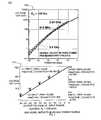
- FIG. 4presents rectifier test data for a sixteen diode rectifier configured in accordance with one embodiment of the present invention.
- FIG. 5is a graph showing the resultant curve representing the data of FIG. 4 of input power versus output voltage configured in accordance with one embodiment of the present invention.
- FIG. 6depicts a Schottky diode configuration in accordance with one embodiment of the present invention.
- FIG. 7shows graphs of performance depicting voltage out for power in configured in accordance with one embodiment of the present invention.
- FIG. 8provides input match (S 11 ) for ports 2 and 3 configured in accordance with one embodiment of the present invention.
- FIG. 9presents data and a circuit model for a sixteen diode rectifier configured in accordance with one embodiment of the present invention.
- FIG. 10is a schematic diagram of a hysteretic switch configured in accordance with one embodiment of the present invention.
- FIG. 11provides data for a hysteretic switch configured in accordance with one embodiment of the present invention.
- FIG. 12is a flow chart depicting a method for a transponder using ambient radiation configured in accordance with one embodiment of the present invention.
- FIG. 1illustrates embodiment 100 of an RFID transponder that operates off of ambient radiation.
- the antenna 105receives RF power from the environment.
- the diode rectifier 110is a high efficiency diode rectifier circuit that converts nano-watt levels of received RF power to milli-volt levels of DC voltage.
- the DC poweris stored in the energy storage element 115 . Once the energy storage element 115 is charged to a pre-defined level, the hysteretic switch 120 will discharge the energy to the low power oscillator 125 .
- Low power oscillator 125operates off of low voltage levels to produce micro-watts of transmit power. The microwatts of power generated from nano-watt levels of received RF energy is transmitted via antenna 130 .
- An optional low current (nanoamps) charging path and small batterymay be added to the energy storage element 115 , allowing for a low duty cycle mode of operation. Battery power consumption is sufficiently low that the battery will last for essentially its shelf life.
- an optional capacitive sensormay be added to the low power oscillator 125 allowing for real-time change detection to take place. The capacitive sensor will shift its value of capacitance based on a sensed change in the environment in which the device is placed. This shift in capacitance will cause the transmitted signal to shift in frequency. A detected shift in transmit frequency can signify the user that a change has occurred.
- FIG. 2depicts embodiment 200 with receive antenna 205 operating at 831 MHz ⁇ 28 to ⁇ 38 dBm.
- 160 to 1600 nWactivate the tag.
- Sixteen diode rectifier 210has output 215 of 50 to 400 millivolts to energy storage element 220 .
- Energy storage element 220 outputis provided to hysteretic switch 225 and nanowatt comparator 230 .
- Nonlimiting embodiment examplesinclude a Maxim® MAX9027 at 1.8 volts at 450 nA.
- Maximis a registered trademark of Maxim Integrated Products, Inc.
- Output of switch 225is 235 50 to 200 millivolts.
- Switch 225 output 235is applied to tunnel diode oscillator 240 .
- Tunnel diode oscillator 240operates at 50 to 200 micro watts (65 millivolts at 1 milliamp, typical) and comprises inductor 245 , Micro-Electro-Mechanical Systems (MEMS) sensor 250 , and tunnel diode 255 .
- output to transmit antenna 260is ⁇ 26 dBm typical at 2 GHz.
- the LC tank circuitdetermines the transmit frequency.
- a nonlimiting embodiment exampleis a transmission of 50 microwatts every 5 mS or 200 microwatts every 20 mS (for a 10 nJ pulse).
- a two diode voltage doublerincreases the voltage sensitivity of a Schottky diode detector when compared to a single diode detector circuit.
- the output voltageis essentially doubled.
- the shunt diodeprovides a DC offset equal to the peak voltage and the series diode acts as the detector.
- the Detector InputInput Sine Wave+DC voltage.
- the Detector OutputInput Sine Wave Voltage, peak-to-peak (double that of a single diode detector).
- the diode impedanceis added in parallel, resulting in a higher capacitive load and a lower series resistance.
- Embodimentsinclude a sixteen diode rectifier.
- FIG. 3is a schematic of a sixteen diode rectifier 300 incorporated in embodiments.
- Sub-componentscomprise a first capacitor 305 , a first diode 310 , a second diode 315 , and a second capacitor 320 forming branches of the rectifier.
- FIG. 4presents rectifier test data 400 for a sixteen diode rectifier.
- Frequencyis 831 MHz and data presented includes power in (Pin) in dBm, and the voltage out (Vout) in millivolts.
- Pinpower in
- Voutvoltage out
- Poutpower in
- FIG. 5is a graph 500 showing the resultant curve represented by the data of FIG. 4 of input power versus output voltage. This is for a tuned circuit ⁇ 20 dB return loss.
- FIG. 6depicts a Schottky diode configuration 600 for modeling. Considerations include package capacitance, leadframe inductance, and bondwire inductance. Modeling components include ports, inductances, capacitances and diodes. Ports include Port 1 605 , Port 2 610 and Port 3 615 . Inductance components include leadframe inductances L 1 0.4 nH 620 , L 2 0.4 nH 625 and L 6 0.4 nH 630 , and bondwire inductances L 3 0.7 nH 635 and L 4 0.7 nH 640 .
- Capacitancesinclude coupling capacitance C 1 0.035 pF 645 , C 2 0.03 pF 650 , and C 3 0.03 pF 655 .
- Diodesinclude diode D 1 660 and diode D 2 665 .
- An ADS HSMS-286Cis representative but not limiting.
- FIG. 9includes data and circuit model 900 for a sixteen diode rectifier.
- Capacitancesinclude C 5 of 47 pF 930 , C 7 of 47 pF 935 , C 8 of 47 pF 940 , C 9 of 47 pF 945 , and C 11 of 47 pF 950 .
- Schottky diode modelsinclude X 1 955 , X 2 960 , and X 3 965 .
- FIG. 10is a schematic diagram 1000 of a hysteretic switch included in embodiments of the invention.
- Active switch 1000comprises resistor R 1 of 10M, R 2 of 10M, R 3 of 200 k, R 4 of 10M, R 5 of 10M, R 6 of 2.2M, where R 1 serves as a trickle charge resister.
- Capacitorsinclude C 1 of 10 ⁇ F and C 2 of 0.1 ⁇ F.
- nanopower comparator U 1which, in nonlimiting embodiments, is a MAX919EUK-T; and single pole, double throw (SPDT) switches S 1 B and S 2 B which, in nonlimiting embodiments, are ADG820 designation switches.
- SPDTsingle pole, double throw
- FIG. 11provides data for an embodiment 1100 of a hysteretic switch.
- Active hysteresis switch waveform 1105provides Cap and Switch out results for ⁇ 2 to +2 seconds over ⁇ 0.5 to +2.5 volts.
- Active hysteresis switch waveform 1110provides Cap and Switch out results for ⁇ 0.005 to +0.005 seconds over ⁇ 0.5 to +2.5 volts.
- Active hysteresis switch positive edge switching time (50 Ohm load) 1115provides Cap and Switch out results for ⁇ 40 to +40 nanoseconds over ⁇ 0.5 to +2.5 volts.
- Active hysteresis switch negative edge switching time (50 Ohm load) 1120provides Cap and Switch out results for ⁇ 40 to +40 nanoseconds over ⁇ 0.5 to +2.5 volts.
- the hysteretic switchtrickle charges batteries and or capacitors. Properties are derived from the input voltage level. Employing a hysteretic switch plus low-power components enables use of very small devices.
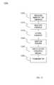
- FIG. 12is a flow chart depicting a method 1200 for a transponder using ambient radiation.
- Ambient radiationis received 1205 , the energy from the ambient radiation is rectified 1210 , energy is stored 1215 , power is switched 1220 , power is modulated by an oscillator 1225 , and a signal is transmitted 1230 .
Landscapes
- Engineering & Computer Science (AREA)
- Computer Hardware Design (AREA)
- Microelectronics & Electronic Packaging (AREA)
- Physics & Mathematics (AREA)
- General Physics & Mathematics (AREA)
- Theoretical Computer Science (AREA)
- Computer Networks & Wireless Communication (AREA)
- Electromagnetism (AREA)
- Near-Field Transmission Systems (AREA)
Abstract
Description
Claims (20)
Priority Applications (1)
| Application Number | Priority Date | Filing Date | Title |
|---|---|---|---|
| US12/644,561US8373543B2 (en) | 2009-12-22 | 2009-12-22 | RFID transponder using ambient radiation |
Applications Claiming Priority (1)
| Application Number | Priority Date | Filing Date | Title |
|---|---|---|---|
| US12/644,561US8373543B2 (en) | 2009-12-22 | 2009-12-22 | RFID transponder using ambient radiation |
Publications (2)
| Publication Number | Publication Date |
|---|---|
| US20110148580A1 US20110148580A1 (en) | 2011-06-23 |
| US8373543B2true US8373543B2 (en) | 2013-02-12 |
Family
ID=44150214
Family Applications (1)
| Application Number | Title | Priority Date | Filing Date |
|---|---|---|---|
| US12/644,561Expired - Fee RelatedUS8373543B2 (en) | 2009-12-22 | 2009-12-22 | RFID transponder using ambient radiation |
Country Status (1)
| Country | Link |
|---|---|
| US (1) | US8373543B2 (en) |
Cited By (12)
| Publication number | Priority date | Publication date | Assignee | Title |
|---|---|---|---|---|
| US9832670B1 (en) | 2016-05-23 | 2017-11-28 | Fat Mongoose Technologies, Inc. | Spectrum analyzing receiver for wireless environment optimization system |
| US10360419B1 (en) | 2018-01-15 | 2019-07-23 | Universal City Studios Llc | Interactive systems and methods with tracking devices |
| US10537803B2 (en) | 2018-01-18 | 2020-01-21 | Universal City Studios Llc | Interactive gaming system |
| US10603564B2 (en) | 2018-01-03 | 2020-03-31 | Universal City Studios Llc | Interactive component for an amusement park |
| US10614271B2 (en) | 2018-01-15 | 2020-04-07 | Universal City Studios Llc | Interactive systems and methods |
| US10653957B2 (en) | 2017-12-06 | 2020-05-19 | Universal City Studios Llc | Interactive video game system |
| US10699084B2 (en) | 2018-01-15 | 2020-06-30 | Universal City Studios Llc | Local interaction systems and methods |
| US10818152B2 (en) | 2018-01-15 | 2020-10-27 | Universal City Studios Llc | Interactive systems and methods with feedback devices |
| US10846967B2 (en) | 2017-12-13 | 2020-11-24 | Universal City Studio LLC | Systems and methods for threshold detection of a wireless device |
| US10845975B2 (en) | 2018-03-29 | 2020-11-24 | Universal City Studios Llc | Interactive animated character head systems and methods |
| US10916059B2 (en) | 2017-12-06 | 2021-02-09 | Universal City Studios Llc | Interactive video game system having an augmented virtual representation |
| US10970725B2 (en) | 2017-11-29 | 2021-04-06 | Universal Studios LLC | System and method for crowd management and maintenance operations |
Families Citing this family (4)
| Publication number | Priority date | Publication date | Assignee | Title |
|---|---|---|---|---|
| CA2807657A1 (en)* | 2010-08-09 | 2012-02-16 | Gabriel Cohn | Sensor systems wirelessly utilizing power infrastructures and associated systems and methods |
| TWI473382B (en)* | 2012-09-28 | 2015-02-11 | Au Optronics Corp | Wireless power transmission device |
| CN103337894A (en)* | 2013-06-18 | 2013-10-02 | 福建华旭新能源技术有限公司 | Intelligent charging transition circuit for storage battery |
| WO2021040594A1 (en)* | 2019-08-30 | 2021-03-04 | Varshney Ambuj | Radio frequency communication device for low power communication |
Citations (13)
| Publication number | Priority date | Publication date | Assignee | Title |
|---|---|---|---|---|
| US4746398A (en)* | 1986-03-21 | 1988-05-24 | Fei Microwave, Inc. | Gallium arsenide planar tunnel diode method |
| US4870419A (en)* | 1980-02-13 | 1989-09-26 | Eid Electronic Identification Systems, Ltd. | Electronic identification system |
| US5652423A (en) | 1994-06-21 | 1997-07-29 | Sony Chemicals Corporation | Non-contacting RF-ID card for wide voltage range input |
| US6101371A (en)* | 1998-09-12 | 2000-08-08 | Lucent Technologies, Inc. | Article comprising an inductor |
| US20020165758A1 (en) | 2001-05-03 | 2002-11-07 | Hind John R. | Identification and tracking of persons using RFID-tagged items |
| US6798716B1 (en) | 2003-06-19 | 2004-09-28 | Bc Systems, Inc. | System and method for wireless electrical power transmission |
| US6924164B2 (en) | 2000-03-24 | 2005-08-02 | Cymbet Corporation | Method of continuous processing of thin-film batteries and like devices |
| US7081693B2 (en)* | 2002-03-07 | 2006-07-25 | Microstrain, Inc. | Energy harvesting for wireless sensor operation and data transmission |
| US20070085689A1 (en) | 2005-10-13 | 2007-04-19 | Bae Systems Information And Electronic Systems Integration Inc. | RFID tag incorporating at least two integrated circuits |
| US7302858B2 (en)* | 2004-09-24 | 2007-12-04 | Kevin Walsh | MEMS capacitive cantilever strain sensor, devices, and formation methods |
| US20070281657A1 (en) | 2005-01-20 | 2007-12-06 | Brommer Karl D | Microradio Design, Manufacturing Method and Applications for the use of Microradios |
| US20080108370A1 (en) | 2005-04-06 | 2008-05-08 | Steve Aninye | System and Method for Tracking, Monitoring, Collecting, Reporting and Communicating with the Movement of Individuals |
| US7970357B2 (en)* | 2007-07-30 | 2011-06-28 | Bae Systems Information And Electronic Systems Integration Inc. | Transponder with stabilized oscillator |
- 2009
- 2009-12-22USUS12/644,561patent/US8373543B2/ennot_activeExpired - Fee Related
Patent Citations (17)
| Publication number | Priority date | Publication date | Assignee | Title |
|---|---|---|---|---|
| US4870419A (en)* | 1980-02-13 | 1989-09-26 | Eid Electronic Identification Systems, Ltd. | Electronic identification system |
| US4746398A (en)* | 1986-03-21 | 1988-05-24 | Fei Microwave, Inc. | Gallium arsenide planar tunnel diode method |
| US5652423A (en) | 1994-06-21 | 1997-07-29 | Sony Chemicals Corporation | Non-contacting RF-ID card for wide voltage range input |
| US5804811A (en) | 1994-06-21 | 1998-09-08 | Sony Chemicals Corporation | Non-contacting RF-ID card for wide voltage range input |
| US6101371A (en)* | 1998-09-12 | 2000-08-08 | Lucent Technologies, Inc. | Article comprising an inductor |
| US7157187B2 (en) | 2000-03-24 | 2007-01-02 | Cymbet Corporation | Thin-film battery devices and apparatus for making the same |
| US7194801B2 (en) | 2000-03-24 | 2007-03-27 | Cymbet Corporation | Thin-film battery having ultra-thin electrolyte and associated method |
| US6924164B2 (en) | 2000-03-24 | 2005-08-02 | Cymbet Corporation | Method of continuous processing of thin-film batteries and like devices |
| US7144655B2 (en) | 2000-03-24 | 2006-12-05 | Cymbet Corporation | Thin-film battery having ultra-thin electrolyte |
| US20020165758A1 (en) | 2001-05-03 | 2002-11-07 | Hind John R. | Identification and tracking of persons using RFID-tagged items |
| US7081693B2 (en)* | 2002-03-07 | 2006-07-25 | Microstrain, Inc. | Energy harvesting for wireless sensor operation and data transmission |
| US6798716B1 (en) | 2003-06-19 | 2004-09-28 | Bc Systems, Inc. | System and method for wireless electrical power transmission |
| US7302858B2 (en)* | 2004-09-24 | 2007-12-04 | Kevin Walsh | MEMS capacitive cantilever strain sensor, devices, and formation methods |
| US20070281657A1 (en) | 2005-01-20 | 2007-12-06 | Brommer Karl D | Microradio Design, Manufacturing Method and Applications for the use of Microradios |
| US20080108370A1 (en) | 2005-04-06 | 2008-05-08 | Steve Aninye | System and Method for Tracking, Monitoring, Collecting, Reporting and Communicating with the Movement of Individuals |
| US20070085689A1 (en) | 2005-10-13 | 2007-04-19 | Bae Systems Information And Electronic Systems Integration Inc. | RFID tag incorporating at least two integrated circuits |
| US7970357B2 (en)* | 2007-07-30 | 2011-06-28 | Bae Systems Information And Electronic Systems Integration Inc. | Transponder with stabilized oscillator |
Cited By (24)
| Publication number | Priority date | Publication date | Assignee | Title |
|---|---|---|---|---|
| US9832670B1 (en) | 2016-05-23 | 2017-11-28 | Fat Mongoose Technologies, Inc. | Spectrum analyzing receiver for wireless environment optimization system |
| US10085159B2 (en) | 2016-05-23 | 2018-09-25 | Fat Mongoose Technologies, Inc. | Wireless environment optimization system |
| US10225748B2 (en) | 2016-05-23 | 2019-03-05 | Fat Mongoose Technologies, Inc. | Beacon for wireless environment optimization system |
| US12086819B2 (en) | 2017-11-29 | 2024-09-10 | Universal City Studios Llc | System and method for crowd management and maintenance operations |
| US11694217B2 (en) | 2017-11-29 | 2023-07-04 | Universal City Studios Llc | System and method for crowd management and maintenance operations |
| US10970725B2 (en) | 2017-11-29 | 2021-04-06 | Universal Studios LLC | System and method for crowd management and maintenance operations |
| US10916059B2 (en) | 2017-12-06 | 2021-02-09 | Universal City Studios Llc | Interactive video game system having an augmented virtual representation |
| US10653957B2 (en) | 2017-12-06 | 2020-05-19 | Universal City Studios Llc | Interactive video game system |
| US11682172B2 (en) | 2017-12-06 | 2023-06-20 | Universal City Studios Llc | Interactive video game system having an augmented virtual representation |
| US11400371B2 (en) | 2017-12-06 | 2022-08-02 | Universal City Studios Llc | Interactive video game system |
| US10846967B2 (en) | 2017-12-13 | 2020-11-24 | Universal City Studio LLC | Systems and methods for threshold detection of a wireless device |
| US10603564B2 (en) | 2018-01-03 | 2020-03-31 | Universal City Studios Llc | Interactive component for an amusement park |
| US11130038B2 (en) | 2018-01-03 | 2021-09-28 | Universal City Studios Llc | Interactive component for an amusement park |
| US10614271B2 (en) | 2018-01-15 | 2020-04-07 | Universal City Studios Llc | Interactive systems and methods |
| US10839178B2 (en) | 2018-01-15 | 2020-11-17 | Universal City Studios Llc | Interactive systems and methods with tracking devices |
| US11379678B2 (en) | 2018-01-15 | 2022-07-05 | Universal City Studios Llc | Local interaction systems and methods |
| US11379679B2 (en) | 2018-01-15 | 2022-07-05 | Universal City Studios Llc | Interactive systems and methods with tracking devices |
| US10818152B2 (en) | 2018-01-15 | 2020-10-27 | Universal City Studios Llc | Interactive systems and methods with feedback devices |
| US10699084B2 (en) | 2018-01-15 | 2020-06-30 | Universal City Studios Llc | Local interaction systems and methods |
| US11983596B2 (en) | 2018-01-15 | 2024-05-14 | Universal City Studios Llc | Interactive systems and methods with tracking devices |
| US10360419B1 (en) | 2018-01-15 | 2019-07-23 | Universal City Studios Llc | Interactive systems and methods with tracking devices |
| US12190194B2 (en) | 2018-01-15 | 2025-01-07 | Universal City Studios, LLC | Local interaction systems and methods |
| US10537803B2 (en) | 2018-01-18 | 2020-01-21 | Universal City Studios Llc | Interactive gaming system |
| US10845975B2 (en) | 2018-03-29 | 2020-11-24 | Universal City Studios Llc | Interactive animated character head systems and methods |
Also Published As
| Publication number | Publication date |
|---|---|
| US20110148580A1 (en) | 2011-06-23 |
Similar Documents
| Publication | Publication Date | Title |
|---|---|---|
| US8373543B2 (en) | RFID transponder using ambient radiation | |
| Naderiparizi et al. | WISPCam: A battery-free RFID camera | |
| Reinisch et al. | A multifrequency passive sensing tag with on-chip temperature sensor and off-chip sensor interface using EPC HF and UHF RFID technology | |
| US10236554B2 (en) | RFID tag battery charging method | |
| ES2620519T3 (en) | System and method for passive measurement of a physical quantity wirelessly | |
| US20100045446A1 (en) | Rfid system using human body communication | |
| KR102703169B1 (en) | Smart tag and object recognition system using the same | |
| EP3249584B1 (en) | A radio frequency identification (rfid) tag and a method of monitoring quality of service (qos) of a rfid tag | |
| Fabbri et al. | Long range battery-less UHF-RFID platform for sensor applications | |
| US10658875B2 (en) | High sensitivity energy harvester | |
| CN111742323A (en) | Method for wirelessly supplying energy by means of radio frequency identification RFID and RFID system | |
| CN102640164A (en) | Self-parameterizing RFID Antenna Extender | |
| La Rosa et al. | A battery-free smart sensor powered with rf energy | |
| CN109698713B (en) | NFC interface with energy management function | |
| Merenda et al. | An autonomous and energy efficient smart sensor platform | |
| CN112949809B (en) | RFID electronic tag and tag power-on communication method | |
| Syed et al. | RF energy harvesting chip powered sensor node | |
| Cartasegna et al. | Smart RFID label for monitoring the preservation conditions of food | |
| EP1958130B1 (en) | Data carrier with sensor | |
| Vaz et al. | Long range, low power UHF RFID analog front-end suitable for batteryless wireless sensors | |
| Safarian et al. | A wirelessly-powered passive RF CMOS transponder with dynamic energy storage and sensitivity enhancement | |
| US8213201B2 (en) | Motion activated amplifier | |
| CN111130601B (en) | Apparatus, and associated method, for communicating via inductive coupling to detect an external tag | |
| US20120050013A1 (en) | Economic Method for Operating a Passive tag | |
| Zuriarrain et al. | A CMOS low frequency analog RFID front-end for the IoT |
Legal Events
| Date | Code | Title | Description |
|---|---|---|---|
| AS | Assignment | Owner name:BAE SYSTEMS INFORMATION AND ELECTRONIC SYSTEMS INT Free format text:ASSIGNMENT OF ASSIGNORS INTEREST;ASSIGNORS:BROMMER, KARL D. DR.;BRITTAIN, CANDICE L.;SUTPHIN, ELDON M.;SIGNING DATES FROM 20091217 TO 20091223;REEL/FRAME:023764/0692 Owner name:BAE SYSTEMS INFORMATION AND ELECTRONIC SYSTEMS INT Free format text:ASSIGNMENT OF ASSIGNORS INTEREST;ASSIGNORS:BROMMER, DR., KARL D.;BRITTAIN, CANDICE L.;SUTPHIN, ELDON M.;SIGNING DATES FROM 20091217 TO 20091223;REEL/FRAME:023765/0585 | |
| STCF | Information on status: patent grant | Free format text:PATENTED CASE | |
| AS | Assignment | Owner name:RADIOFIDO LLC, NEW HAMPSHIRE Free format text:ASSIGNMENT OF ASSIGNORS INTEREST;ASSIGNOR:BAE SYSTEMS INFORMATION AND ELECTRONIC SYSTEMS INTEGRATION INC.;REEL/FRAME:030132/0089 Effective date:20130115 | |
| FPAY | Fee payment | Year of fee payment:4 | |
| FEPP | Fee payment procedure | Free format text:MAINTENANCE FEE REMINDER MAILED (ORIGINAL EVENT CODE: REM.); ENTITY STATUS OF PATENT OWNER: LARGE ENTITY | |
| LAPS | Lapse for failure to pay maintenance fees | Free format text:PATENT EXPIRED FOR FAILURE TO PAY MAINTENANCE FEES (ORIGINAL EVENT CODE: EXP.); ENTITY STATUS OF PATENT OWNER: LARGE ENTITY | |
| STCH | Information on status: patent discontinuation | Free format text:PATENT EXPIRED DUE TO NONPAYMENT OF MAINTENANCE FEES UNDER 37 CFR 1.362 | |
| FP | Lapsed due to failure to pay maintenance fee | Effective date:20210212 | |
| PRDP | Patent reinstated due to the acceptance of a late maintenance fee | Effective date:20220318 | |
| FEPP | Fee payment procedure | Free format text:PETITION RELATED TO MAINTENANCE FEES FILED (ORIGINAL EVENT CODE: PMFP); ENTITY STATUS OF PATENT OWNER: LARGE ENTITY Free format text:PETITION RELATED TO MAINTENANCE FEES GRANTED (ORIGINAL EVENT CODE: PMFG); ENTITY STATUS OF PATENT OWNER: LARGE ENTITY Free format text:SURCHARGE, PETITION TO ACCEPT PYMT AFTER EXP, UNINTENTIONAL (ORIGINAL EVENT CODE: M1558); ENTITY STATUS OF PATENT OWNER: LARGE ENTITY | |
| MAFP | Maintenance fee payment | Free format text:PAYMENT OF MAINTENANCE FEE, 8TH YEAR, LARGE ENTITY (ORIGINAL EVENT CODE: M1552); ENTITY STATUS OF PATENT OWNER: LARGE ENTITY Year of fee payment:8 | |
| STCF | Information on status: patent grant | Free format text:PATENTED CASE | |
| FEPP | Fee payment procedure | Free format text:MAINTENANCE FEE REMINDER MAILED (ORIGINAL EVENT CODE: REM.); ENTITY STATUS OF PATENT OWNER: LARGE ENTITY | |
| LAPS | Lapse for failure to pay maintenance fees | Free format text:PATENT EXPIRED FOR FAILURE TO PAY MAINTENANCE FEES (ORIGINAL EVENT CODE: EXP.); ENTITY STATUS OF PATENT OWNER: LARGE ENTITY | |
| STCH | Information on status: patent discontinuation | Free format text:PATENT EXPIRED DUE TO NONPAYMENT OF MAINTENANCE FEES UNDER 37 CFR 1.362 | |
| FP | Lapsed due to failure to pay maintenance fee | Effective date:20250212 |