US8372741B1 - Method for package-on-package assembly with wire bonds to encapsulation surface - Google Patents
Method for package-on-package assembly with wire bonds to encapsulation surfaceDownload PDFInfo
- Publication number
- US8372741B1 US8372741B1US13/405,125US201213405125AUS8372741B1US 8372741 B1US8372741 B1US 8372741B1US 201213405125 AUS201213405125 AUS 201213405125AUS 8372741 B1US8372741 B1US 8372741B1
- Authority
- US
- United States
- Prior art keywords
- wire
- substrate
- bond
- encapsulation layer
- cut
- Prior art date
- Legal status (The legal status is an assumption and is not a legal conclusion. Google has not performed a legal analysis and makes no representation as to the accuracy of the status listed.)
- Active
Links
Images


Classifications
- H—ELECTRICITY
- H01—ELECTRIC ELEMENTS
- H01L—SEMICONDUCTOR DEVICES NOT COVERED BY CLASS H10
- H01L23/00—Details of semiconductor or other solid state devices
- H01L23/28—Encapsulations, e.g. encapsulating layers, coatings, e.g. for protection
- H01L23/31—Encapsulations, e.g. encapsulating layers, coatings, e.g. for protection characterised by the arrangement or shape
- H01L23/3107—Encapsulations, e.g. encapsulating layers, coatings, e.g. for protection characterised by the arrangement or shape the device being completely enclosed
- H01L23/3121—Encapsulations, e.g. encapsulating layers, coatings, e.g. for protection characterised by the arrangement or shape the device being completely enclosed a substrate forming part of the encapsulation
- H01L23/3128—Encapsulations, e.g. encapsulating layers, coatings, e.g. for protection characterised by the arrangement or shape the device being completely enclosed a substrate forming part of the encapsulation the substrate having spherical bumps for external connection
- H—ELECTRICITY
- H01—ELECTRIC ELEMENTS
- H01L—SEMICONDUCTOR DEVICES NOT COVERED BY CLASS H10
- H01L21/00—Processes or apparatus adapted for the manufacture or treatment of semiconductor or solid state devices or of parts thereof
- H01L21/02—Manufacture or treatment of semiconductor devices or of parts thereof
- H01L21/04—Manufacture or treatment of semiconductor devices or of parts thereof the devices having potential barriers, e.g. a PN junction, depletion layer or carrier concentration layer
- H01L21/48—Manufacture or treatment of parts, e.g. containers, prior to assembly of the devices, using processes not provided for in a single one of the groups H01L21/18 - H01L21/326 or H10D48/04 - H10D48/07
- H01L21/4814—Conductive parts
- H01L21/4846—Leads on or in insulating or insulated substrates, e.g. metallisation
- H01L21/4853—Connection or disconnection of other leads to or from a metallisation, e.g. pins, wires, bumps
- H—ELECTRICITY
- H01—ELECTRIC ELEMENTS
- H01L—SEMICONDUCTOR DEVICES NOT COVERED BY CLASS H10
- H01L23/00—Details of semiconductor or other solid state devices
- H01L23/28—Encapsulations, e.g. encapsulating layers, coatings, e.g. for protection
- H01L23/31—Encapsulations, e.g. encapsulating layers, coatings, e.g. for protection characterised by the arrangement or shape
- H01L23/3107—Encapsulations, e.g. encapsulating layers, coatings, e.g. for protection characterised by the arrangement or shape the device being completely enclosed
- H01L23/3121—Encapsulations, e.g. encapsulating layers, coatings, e.g. for protection characterised by the arrangement or shape the device being completely enclosed a substrate forming part of the encapsulation
- H—ELECTRICITY
- H01—ELECTRIC ELEMENTS
- H01L—SEMICONDUCTOR DEVICES NOT COVERED BY CLASS H10
- H01L23/00—Details of semiconductor or other solid state devices
- H01L23/48—Arrangements for conducting electric current to or from the solid state body in operation, e.g. leads, terminal arrangements ; Selection of materials therefor
- H01L23/488—Arrangements for conducting electric current to or from the solid state body in operation, e.g. leads, terminal arrangements ; Selection of materials therefor consisting of soldered or bonded constructions
- H01L23/495—Lead-frames or other flat leads
- H01L23/49517—Additional leads
- H—ELECTRICITY
- H01—ELECTRIC ELEMENTS
- H01L—SEMICONDUCTOR DEVICES NOT COVERED BY CLASS H10
- H01L23/00—Details of semiconductor or other solid state devices
- H01L23/48—Arrangements for conducting electric current to or from the solid state body in operation, e.g. leads, terminal arrangements ; Selection of materials therefor
- H01L23/488—Arrangements for conducting electric current to or from the solid state body in operation, e.g. leads, terminal arrangements ; Selection of materials therefor consisting of soldered or bonded constructions
- H01L23/498—Leads, i.e. metallisations or lead-frames on insulating substrates, e.g. chip carriers
- H01L23/49811—Additional leads joined to the metallisation on the insulating substrate, e.g. pins, bumps, wires, flat leads
- H—ELECTRICITY
- H01—ELECTRIC ELEMENTS
- H01L—SEMICONDUCTOR DEVICES NOT COVERED BY CLASS H10
- H01L24/00—Arrangements for connecting or disconnecting semiconductor or solid-state bodies; Methods or apparatus related thereto
- H01L24/01—Means for bonding being attached to, or being formed on, the surface to be connected, e.g. chip-to-package, die-attach, "first-level" interconnects; Manufacturing methods related thereto
- H01L24/02—Bonding areas ; Manufacturing methods related thereto
- H01L24/03—Manufacturing methods
- H—ELECTRICITY
- H01—ELECTRIC ELEMENTS
- H01L—SEMICONDUCTOR DEVICES NOT COVERED BY CLASS H10
- H01L24/00—Arrangements for connecting or disconnecting semiconductor or solid-state bodies; Methods or apparatus related thereto
- H01L24/01—Means for bonding being attached to, or being formed on, the surface to be connected, e.g. chip-to-package, die-attach, "first-level" interconnects; Manufacturing methods related thereto
- H01L24/02—Bonding areas ; Manufacturing methods related thereto
- H01L24/04—Structure, shape, material or disposition of the bonding areas prior to the connecting process
- H01L24/06—Structure, shape, material or disposition of the bonding areas prior to the connecting process of a plurality of bonding areas
- H—ELECTRICITY
- H01—ELECTRIC ELEMENTS
- H01L—SEMICONDUCTOR DEVICES NOT COVERED BY CLASS H10
- H01L24/00—Arrangements for connecting or disconnecting semiconductor or solid-state bodies; Methods or apparatus related thereto
- H01L24/01—Means for bonding being attached to, or being formed on, the surface to be connected, e.g. chip-to-package, die-attach, "first-level" interconnects; Manufacturing methods related thereto
- H01L24/42—Wire connectors; Manufacturing methods related thereto
- H01L24/47—Structure, shape, material or disposition of the wire connectors after the connecting process
- H01L24/49—Structure, shape, material or disposition of the wire connectors after the connecting process of a plurality of wire connectors
- H—ELECTRICITY
- H01—ELECTRIC ELEMENTS
- H01L—SEMICONDUCTOR DEVICES NOT COVERED BY CLASS H10
- H01L25/00—Assemblies consisting of a plurality of semiconductor or other solid state devices
- H01L25/03—Assemblies consisting of a plurality of semiconductor or other solid state devices all the devices being of a type provided for in a single subclass of subclasses H10B, H10D, H10F, H10H, H10K or H10N, e.g. assemblies of rectifier diodes
- H01L25/04—Assemblies consisting of a plurality of semiconductor or other solid state devices all the devices being of a type provided for in a single subclass of subclasses H10B, H10D, H10F, H10H, H10K or H10N, e.g. assemblies of rectifier diodes the devices not having separate containers
- H01L25/065—Assemblies consisting of a plurality of semiconductor or other solid state devices all the devices being of a type provided for in a single subclass of subclasses H10B, H10D, H10F, H10H, H10K or H10N, e.g. assemblies of rectifier diodes the devices not having separate containers the devices being of a type provided for in group H10D89/00
- H01L25/0657—Stacked arrangements of devices
- H—ELECTRICITY
- H01—ELECTRIC ELEMENTS
- H01L—SEMICONDUCTOR DEVICES NOT COVERED BY CLASS H10
- H01L25/00—Assemblies consisting of a plurality of semiconductor or other solid state devices
- H01L25/03—Assemblies consisting of a plurality of semiconductor or other solid state devices all the devices being of a type provided for in a single subclass of subclasses H10B, H10D, H10F, H10H, H10K or H10N, e.g. assemblies of rectifier diodes
- H01L25/10—Assemblies consisting of a plurality of semiconductor or other solid state devices all the devices being of a type provided for in a single subclass of subclasses H10B, H10D, H10F, H10H, H10K or H10N, e.g. assemblies of rectifier diodes the devices having separate containers
- H01L25/105—Assemblies consisting of a plurality of semiconductor or other solid state devices all the devices being of a type provided for in a single subclass of subclasses H10B, H10D, H10F, H10H, H10K or H10N, e.g. assemblies of rectifier diodes the devices having separate containers the devices being integrated devices of class H10
- H—ELECTRICITY
- H01—ELECTRIC ELEMENTS
- H01L—SEMICONDUCTOR DEVICES NOT COVERED BY CLASS H10
- H01L2224/00—Indexing scheme for arrangements for connecting or disconnecting semiconductor or solid-state bodies and methods related thereto as covered by H01L24/00
- H01L2224/01—Means for bonding being attached to, or being formed on, the surface to be connected, e.g. chip-to-package, die-attach, "first-level" interconnects; Manufacturing methods related thereto
- H01L2224/02—Bonding areas; Manufacturing methods related thereto
- H01L2224/04—Structure, shape, material or disposition of the bonding areas prior to the connecting process
- H01L2224/0401—Bonding areas specifically adapted for bump connectors, e.g. under bump metallisation [UBM]
- H—ELECTRICITY
- H01—ELECTRIC ELEMENTS
- H01L—SEMICONDUCTOR DEVICES NOT COVERED BY CLASS H10
- H01L2224/00—Indexing scheme for arrangements for connecting or disconnecting semiconductor or solid-state bodies and methods related thereto as covered by H01L24/00
- H01L2224/01—Means for bonding being attached to, or being formed on, the surface to be connected, e.g. chip-to-package, die-attach, "first-level" interconnects; Manufacturing methods related thereto
- H01L2224/02—Bonding areas; Manufacturing methods related thereto
- H01L2224/04—Structure, shape, material or disposition of the bonding areas prior to the connecting process
- H01L2224/04042—Bonding areas specifically adapted for wire connectors, e.g. wirebond pads
- H—ELECTRICITY
- H01—ELECTRIC ELEMENTS
- H01L—SEMICONDUCTOR DEVICES NOT COVERED BY CLASS H10
- H01L2224/00—Indexing scheme for arrangements for connecting or disconnecting semiconductor or solid-state bodies and methods related thereto as covered by H01L24/00
- H01L2224/01—Means for bonding being attached to, or being formed on, the surface to be connected, e.g. chip-to-package, die-attach, "first-level" interconnects; Manufacturing methods related thereto
- H01L2224/10—Bump connectors; Manufacturing methods related thereto
- H01L2224/12—Structure, shape, material or disposition of the bump connectors prior to the connecting process
- H01L2224/13—Structure, shape, material or disposition of the bump connectors prior to the connecting process of an individual bump connector
- H01L2224/13001—Core members of the bump connector
- H01L2224/13099—Material
- H01L2224/131—Material with a principal constituent of the material being a metal or a metalloid, e.g. boron [B], silicon [Si], germanium [Ge], arsenic [As], antimony [Sb], tellurium [Te] and polonium [Po], and alloys thereof
- H—ELECTRICITY
- H01—ELECTRIC ELEMENTS
- H01L—SEMICONDUCTOR DEVICES NOT COVERED BY CLASS H10
- H01L2224/00—Indexing scheme for arrangements for connecting or disconnecting semiconductor or solid-state bodies and methods related thereto as covered by H01L24/00
- H01L2224/01—Means for bonding being attached to, or being formed on, the surface to be connected, e.g. chip-to-package, die-attach, "first-level" interconnects; Manufacturing methods related thereto
- H01L2224/10—Bump connectors; Manufacturing methods related thereto
- H01L2224/15—Structure, shape, material or disposition of the bump connectors after the connecting process
- H01L2224/16—Structure, shape, material or disposition of the bump connectors after the connecting process of an individual bump connector
- H01L2224/161—Disposition
- H01L2224/16135—Disposition the bump connector connecting between different semiconductor or solid-state bodies, i.e. chip-to-chip
- H01L2224/16145—Disposition the bump connector connecting between different semiconductor or solid-state bodies, i.e. chip-to-chip the bodies being stacked
- H—ELECTRICITY
- H01—ELECTRIC ELEMENTS
- H01L—SEMICONDUCTOR DEVICES NOT COVERED BY CLASS H10
- H01L2224/00—Indexing scheme for arrangements for connecting or disconnecting semiconductor or solid-state bodies and methods related thereto as covered by H01L24/00
- H01L2224/01—Means for bonding being attached to, or being formed on, the surface to be connected, e.g. chip-to-package, die-attach, "first-level" interconnects; Manufacturing methods related thereto
- H01L2224/10—Bump connectors; Manufacturing methods related thereto
- H01L2224/15—Structure, shape, material or disposition of the bump connectors after the connecting process
- H01L2224/16—Structure, shape, material or disposition of the bump connectors after the connecting process of an individual bump connector
- H01L2224/161—Disposition
- H01L2224/16151—Disposition the bump connector connecting between a semiconductor or solid-state body and an item not being a semiconductor or solid-state body, e.g. chip-to-substrate, chip-to-passive
- H01L2224/16221—Disposition the bump connector connecting between a semiconductor or solid-state body and an item not being a semiconductor or solid-state body, e.g. chip-to-substrate, chip-to-passive the body and the item being stacked
- H01L2224/16225—Disposition the bump connector connecting between a semiconductor or solid-state body and an item not being a semiconductor or solid-state body, e.g. chip-to-substrate, chip-to-passive the body and the item being stacked the item being non-metallic, e.g. insulating substrate with or without metallisation
- H01L2224/16227—Disposition the bump connector connecting between a semiconductor or solid-state body and an item not being a semiconductor or solid-state body, e.g. chip-to-substrate, chip-to-passive the body and the item being stacked the item being non-metallic, e.g. insulating substrate with or without metallisation the bump connector connecting to a bond pad of the item
- H—ELECTRICITY
- H01—ELECTRIC ELEMENTS
- H01L—SEMICONDUCTOR DEVICES NOT COVERED BY CLASS H10
- H01L2224/00—Indexing scheme for arrangements for connecting or disconnecting semiconductor or solid-state bodies and methods related thereto as covered by H01L24/00
- H01L2224/01—Means for bonding being attached to, or being formed on, the surface to be connected, e.g. chip-to-package, die-attach, "first-level" interconnects; Manufacturing methods related thereto
- H01L2224/26—Layer connectors, e.g. plate connectors, solder or adhesive layers; Manufacturing methods related thereto
- H01L2224/31—Structure, shape, material or disposition of the layer connectors after the connecting process
- H01L2224/32—Structure, shape, material or disposition of the layer connectors after the connecting process of an individual layer connector
- H01L2224/321—Disposition
- H01L2224/32151—Disposition the layer connector connecting between a semiconductor or solid-state body and an item not being a semiconductor or solid-state body, e.g. chip-to-substrate, chip-to-passive
- H01L2224/32221—Disposition the layer connector connecting between a semiconductor or solid-state body and an item not being a semiconductor or solid-state body, e.g. chip-to-substrate, chip-to-passive the body and the item being stacked
- H01L2224/32225—Disposition the layer connector connecting between a semiconductor or solid-state body and an item not being a semiconductor or solid-state body, e.g. chip-to-substrate, chip-to-passive the body and the item being stacked the item being non-metallic, e.g. insulating substrate with or without metallisation
- H—ELECTRICITY
- H01—ELECTRIC ELEMENTS
- H01L—SEMICONDUCTOR DEVICES NOT COVERED BY CLASS H10
- H01L2224/00—Indexing scheme for arrangements for connecting or disconnecting semiconductor or solid-state bodies and methods related thereto as covered by H01L24/00
- H01L2224/01—Means for bonding being attached to, or being formed on, the surface to be connected, e.g. chip-to-package, die-attach, "first-level" interconnects; Manufacturing methods related thereto
- H01L2224/26—Layer connectors, e.g. plate connectors, solder or adhesive layers; Manufacturing methods related thereto
- H01L2224/31—Structure, shape, material or disposition of the layer connectors after the connecting process
- H01L2224/32—Structure, shape, material or disposition of the layer connectors after the connecting process of an individual layer connector
- H01L2224/321—Disposition
- H01L2224/32151—Disposition the layer connector connecting between a semiconductor or solid-state body and an item not being a semiconductor or solid-state body, e.g. chip-to-substrate, chip-to-passive
- H01L2224/32221—Disposition the layer connector connecting between a semiconductor or solid-state body and an item not being a semiconductor or solid-state body, e.g. chip-to-substrate, chip-to-passive the body and the item being stacked
- H01L2224/32245—Disposition the layer connector connecting between a semiconductor or solid-state body and an item not being a semiconductor or solid-state body, e.g. chip-to-substrate, chip-to-passive the body and the item being stacked the item being metallic
- H—ELECTRICITY
- H01—ELECTRIC ELEMENTS
- H01L—SEMICONDUCTOR DEVICES NOT COVERED BY CLASS H10
- H01L2224/00—Indexing scheme for arrangements for connecting or disconnecting semiconductor or solid-state bodies and methods related thereto as covered by H01L24/00
- H01L2224/01—Means for bonding being attached to, or being formed on, the surface to be connected, e.g. chip-to-package, die-attach, "first-level" interconnects; Manufacturing methods related thereto
- H01L2224/42—Wire connectors; Manufacturing methods related thereto
- H01L2224/44—Structure, shape, material or disposition of the wire connectors prior to the connecting process
- H01L2224/45—Structure, shape, material or disposition of the wire connectors prior to the connecting process of an individual wire connector
- H01L2224/45001—Core members of the connector
- H01L2224/45099—Material
- H01L2224/451—Material with a principal constituent of the material being a metal or a metalloid, e.g. boron (B), silicon (Si), germanium (Ge), arsenic (As), antimony (Sb), tellurium (Te) and polonium (Po), and alloys thereof
- H01L2224/45117—Material with a principal constituent of the material being a metal or a metalloid, e.g. boron (B), silicon (Si), germanium (Ge), arsenic (As), antimony (Sb), tellurium (Te) and polonium (Po), and alloys thereof the principal constituent melting at a temperature of greater than or equal to 400°C and less than 950°C
- H01L2224/45124—Aluminium (Al) as principal constituent
- H—ELECTRICITY
- H01—ELECTRIC ELEMENTS
- H01L—SEMICONDUCTOR DEVICES NOT COVERED BY CLASS H10
- H01L2224/00—Indexing scheme for arrangements for connecting or disconnecting semiconductor or solid-state bodies and methods related thereto as covered by H01L24/00
- H01L2224/01—Means for bonding being attached to, or being formed on, the surface to be connected, e.g. chip-to-package, die-attach, "first-level" interconnects; Manufacturing methods related thereto
- H01L2224/42—Wire connectors; Manufacturing methods related thereto
- H01L2224/44—Structure, shape, material or disposition of the wire connectors prior to the connecting process
- H01L2224/45—Structure, shape, material or disposition of the wire connectors prior to the connecting process of an individual wire connector
- H01L2224/45001—Core members of the connector
- H01L2224/45099—Material
- H01L2224/451—Material with a principal constituent of the material being a metal or a metalloid, e.g. boron (B), silicon (Si), germanium (Ge), arsenic (As), antimony (Sb), tellurium (Te) and polonium (Po), and alloys thereof
- H01L2224/45138—Material with a principal constituent of the material being a metal or a metalloid, e.g. boron (B), silicon (Si), germanium (Ge), arsenic (As), antimony (Sb), tellurium (Te) and polonium (Po), and alloys thereof the principal constituent melting at a temperature of greater than or equal to 950°C and less than 1550°C
- H01L2224/45144—Gold (Au) as principal constituent
- H—ELECTRICITY
- H01—ELECTRIC ELEMENTS
- H01L—SEMICONDUCTOR DEVICES NOT COVERED BY CLASS H10
- H01L2224/00—Indexing scheme for arrangements for connecting or disconnecting semiconductor or solid-state bodies and methods related thereto as covered by H01L24/00
- H01L2224/01—Means for bonding being attached to, or being formed on, the surface to be connected, e.g. chip-to-package, die-attach, "first-level" interconnects; Manufacturing methods related thereto
- H01L2224/42—Wire connectors; Manufacturing methods related thereto
- H01L2224/44—Structure, shape, material or disposition of the wire connectors prior to the connecting process
- H01L2224/45—Structure, shape, material or disposition of the wire connectors prior to the connecting process of an individual wire connector
- H01L2224/45001—Core members of the connector
- H01L2224/45099—Material
- H01L2224/451—Material with a principal constituent of the material being a metal or a metalloid, e.g. boron (B), silicon (Si), germanium (Ge), arsenic (As), antimony (Sb), tellurium (Te) and polonium (Po), and alloys thereof
- H01L2224/45138—Material with a principal constituent of the material being a metal or a metalloid, e.g. boron (B), silicon (Si), germanium (Ge), arsenic (As), antimony (Sb), tellurium (Te) and polonium (Po), and alloys thereof the principal constituent melting at a temperature of greater than or equal to 950°C and less than 1550°C
- H01L2224/45147—Copper (Cu) as principal constituent
- H—ELECTRICITY
- H01—ELECTRIC ELEMENTS
- H01L—SEMICONDUCTOR DEVICES NOT COVERED BY CLASS H10
- H01L2224/00—Indexing scheme for arrangements for connecting or disconnecting semiconductor or solid-state bodies and methods related thereto as covered by H01L24/00
- H01L2224/01—Means for bonding being attached to, or being formed on, the surface to be connected, e.g. chip-to-package, die-attach, "first-level" interconnects; Manufacturing methods related thereto
- H01L2224/42—Wire connectors; Manufacturing methods related thereto
- H01L2224/44—Structure, shape, material or disposition of the wire connectors prior to the connecting process
- H01L2224/45—Structure, shape, material or disposition of the wire connectors prior to the connecting process of an individual wire connector
- H01L2224/45001—Core members of the connector
- H01L2224/45099—Material
- H01L2224/451—Material with a principal constituent of the material being a metal or a metalloid, e.g. boron (B), silicon (Si), germanium (Ge), arsenic (As), antimony (Sb), tellurium (Te) and polonium (Po), and alloys thereof
- H01L2224/45138—Material with a principal constituent of the material being a metal or a metalloid, e.g. boron (B), silicon (Si), germanium (Ge), arsenic (As), antimony (Sb), tellurium (Te) and polonium (Po), and alloys thereof the principal constituent melting at a temperature of greater than or equal to 950°C and less than 1550°C
- H01L2224/45155—Nickel (Ni) as principal constituent
- H—ELECTRICITY
- H01—ELECTRIC ELEMENTS
- H01L—SEMICONDUCTOR DEVICES NOT COVERED BY CLASS H10
- H01L2224/00—Indexing scheme for arrangements for connecting or disconnecting semiconductor or solid-state bodies and methods related thereto as covered by H01L24/00
- H01L2224/01—Means for bonding being attached to, or being formed on, the surface to be connected, e.g. chip-to-package, die-attach, "first-level" interconnects; Manufacturing methods related thereto
- H01L2224/42—Wire connectors; Manufacturing methods related thereto
- H01L2224/47—Structure, shape, material or disposition of the wire connectors after the connecting process
- H01L2224/48—Structure, shape, material or disposition of the wire connectors after the connecting process of an individual wire connector
- H01L2224/4805—Shape
- H01L2224/4809—Loop shape
- H01L2224/48091—Arched
- H—ELECTRICITY
- H01—ELECTRIC ELEMENTS
- H01L—SEMICONDUCTOR DEVICES NOT COVERED BY CLASS H10
- H01L2224/00—Indexing scheme for arrangements for connecting or disconnecting semiconductor or solid-state bodies and methods related thereto as covered by H01L24/00
- H01L2224/01—Means for bonding being attached to, or being formed on, the surface to be connected, e.g. chip-to-package, die-attach, "first-level" interconnects; Manufacturing methods related thereto
- H01L2224/42—Wire connectors; Manufacturing methods related thereto
- H01L2224/47—Structure, shape, material or disposition of the wire connectors after the connecting process
- H01L2224/48—Structure, shape, material or disposition of the wire connectors after the connecting process of an individual wire connector
- H01L2224/481—Disposition
- H01L2224/48135—Connecting between different semiconductor or solid-state bodies, i.e. chip-to-chip
- H01L2224/48145—Connecting between different semiconductor or solid-state bodies, i.e. chip-to-chip the bodies being stacked
- H—ELECTRICITY
- H01—ELECTRIC ELEMENTS
- H01L—SEMICONDUCTOR DEVICES NOT COVERED BY CLASS H10
- H01L2224/00—Indexing scheme for arrangements for connecting or disconnecting semiconductor or solid-state bodies and methods related thereto as covered by H01L24/00
- H01L2224/01—Means for bonding being attached to, or being formed on, the surface to be connected, e.g. chip-to-package, die-attach, "first-level" interconnects; Manufacturing methods related thereto
- H01L2224/42—Wire connectors; Manufacturing methods related thereto
- H01L2224/47—Structure, shape, material or disposition of the wire connectors after the connecting process
- H01L2224/48—Structure, shape, material or disposition of the wire connectors after the connecting process of an individual wire connector
- H01L2224/481—Disposition
- H01L2224/48151—Connecting between a semiconductor or solid-state body and an item not being a semiconductor or solid-state body, e.g. chip-to-substrate, chip-to-passive
- H01L2224/48221—Connecting between a semiconductor or solid-state body and an item not being a semiconductor or solid-state body, e.g. chip-to-substrate, chip-to-passive the body and the item being stacked
- H01L2224/48225—Connecting between a semiconductor or solid-state body and an item not being a semiconductor or solid-state body, e.g. chip-to-substrate, chip-to-passive the body and the item being stacked the item being non-metallic, e.g. insulating substrate with or without metallisation
- H01L2224/48227—Connecting between a semiconductor or solid-state body and an item not being a semiconductor or solid-state body, e.g. chip-to-substrate, chip-to-passive the body and the item being stacked the item being non-metallic, e.g. insulating substrate with or without metallisation connecting the wire to a bond pad of the item
- H—ELECTRICITY
- H01—ELECTRIC ELEMENTS
- H01L—SEMICONDUCTOR DEVICES NOT COVERED BY CLASS H10
- H01L2224/00—Indexing scheme for arrangements for connecting or disconnecting semiconductor or solid-state bodies and methods related thereto as covered by H01L24/00
- H01L2224/01—Means for bonding being attached to, or being formed on, the surface to be connected, e.g. chip-to-package, die-attach, "first-level" interconnects; Manufacturing methods related thereto
- H01L2224/42—Wire connectors; Manufacturing methods related thereto
- H01L2224/47—Structure, shape, material or disposition of the wire connectors after the connecting process
- H01L2224/48—Structure, shape, material or disposition of the wire connectors after the connecting process of an individual wire connector
- H01L2224/481—Disposition
- H01L2224/48151—Connecting between a semiconductor or solid-state body and an item not being a semiconductor or solid-state body, e.g. chip-to-substrate, chip-to-passive
- H01L2224/48221—Connecting between a semiconductor or solid-state body and an item not being a semiconductor or solid-state body, e.g. chip-to-substrate, chip-to-passive the body and the item being stacked
- H01L2224/48225—Connecting between a semiconductor or solid-state body and an item not being a semiconductor or solid-state body, e.g. chip-to-substrate, chip-to-passive the body and the item being stacked the item being non-metallic, e.g. insulating substrate with or without metallisation
- H01L2224/4824—Connecting between the body and an opposite side of the item with respect to the body
- H—ELECTRICITY
- H01—ELECTRIC ELEMENTS
- H01L—SEMICONDUCTOR DEVICES NOT COVERED BY CLASS H10
- H01L2224/00—Indexing scheme for arrangements for connecting or disconnecting semiconductor or solid-state bodies and methods related thereto as covered by H01L24/00
- H01L2224/01—Means for bonding being attached to, or being formed on, the surface to be connected, e.g. chip-to-package, die-attach, "first-level" interconnects; Manufacturing methods related thereto
- H01L2224/42—Wire connectors; Manufacturing methods related thereto
- H01L2224/47—Structure, shape, material or disposition of the wire connectors after the connecting process
- H01L2224/48—Structure, shape, material or disposition of the wire connectors after the connecting process of an individual wire connector
- H01L2224/481—Disposition
- H01L2224/48151—Connecting between a semiconductor or solid-state body and an item not being a semiconductor or solid-state body, e.g. chip-to-substrate, chip-to-passive
- H01L2224/48221—Connecting between a semiconductor or solid-state body and an item not being a semiconductor or solid-state body, e.g. chip-to-substrate, chip-to-passive the body and the item being stacked
- H01L2224/48245—Connecting between a semiconductor or solid-state body and an item not being a semiconductor or solid-state body, e.g. chip-to-substrate, chip-to-passive the body and the item being stacked the item being metallic
- H01L2224/48247—Connecting between a semiconductor or solid-state body and an item not being a semiconductor or solid-state body, e.g. chip-to-substrate, chip-to-passive the body and the item being stacked the item being metallic connecting the wire to a bond pad of the item
- H—ELECTRICITY
- H01—ELECTRIC ELEMENTS
- H01L—SEMICONDUCTOR DEVICES NOT COVERED BY CLASS H10
- H01L2224/00—Indexing scheme for arrangements for connecting or disconnecting semiconductor or solid-state bodies and methods related thereto as covered by H01L24/00
- H01L2224/01—Means for bonding being attached to, or being formed on, the surface to be connected, e.g. chip-to-package, die-attach, "first-level" interconnects; Manufacturing methods related thereto
- H01L2224/42—Wire connectors; Manufacturing methods related thereto
- H01L2224/47—Structure, shape, material or disposition of the wire connectors after the connecting process
- H01L2224/49—Structure, shape, material or disposition of the wire connectors after the connecting process of a plurality of wire connectors
- H01L2224/491—Disposition
- H01L2224/4912—Layout
- H01L2224/49171—Fan-out arrangements
- H—ELECTRICITY
- H01—ELECTRIC ELEMENTS
- H01L—SEMICONDUCTOR DEVICES NOT COVERED BY CLASS H10
- H01L2224/00—Indexing scheme for arrangements for connecting or disconnecting semiconductor or solid-state bodies and methods related thereto as covered by H01L24/00
- H01L2224/73—Means for bonding being of different types provided for in two or more of groups H01L2224/10, H01L2224/18, H01L2224/26, H01L2224/34, H01L2224/42, H01L2224/50, H01L2224/63, H01L2224/71
- H01L2224/732—Location after the connecting process
- H01L2224/73201—Location after the connecting process on the same surface
- H01L2224/73203—Bump and layer connectors
- H01L2224/73204—Bump and layer connectors the bump connector being embedded into the layer connector
- H—ELECTRICITY
- H01—ELECTRIC ELEMENTS
- H01L—SEMICONDUCTOR DEVICES NOT COVERED BY CLASS H10
- H01L2224/00—Indexing scheme for arrangements for connecting or disconnecting semiconductor or solid-state bodies and methods related thereto as covered by H01L24/00
- H01L2224/73—Means for bonding being of different types provided for in two or more of groups H01L2224/10, H01L2224/18, H01L2224/26, H01L2224/34, H01L2224/42, H01L2224/50, H01L2224/63, H01L2224/71
- H01L2224/732—Location after the connecting process
- H01L2224/73201—Location after the connecting process on the same surface
- H01L2224/73215—Layer and wire connectors
- H—ELECTRICITY
- H01—ELECTRIC ELEMENTS
- H01L—SEMICONDUCTOR DEVICES NOT COVERED BY CLASS H10
- H01L2224/00—Indexing scheme for arrangements for connecting or disconnecting semiconductor or solid-state bodies and methods related thereto as covered by H01L24/00
- H01L2224/73—Means for bonding being of different types provided for in two or more of groups H01L2224/10, H01L2224/18, H01L2224/26, H01L2224/34, H01L2224/42, H01L2224/50, H01L2224/63, H01L2224/71
- H01L2224/732—Location after the connecting process
- H01L2224/73251—Location after the connecting process on different surfaces
- H01L2224/73265—Layer and wire connectors
- H—ELECTRICITY
- H01—ELECTRIC ELEMENTS
- H01L—SEMICONDUCTOR DEVICES NOT COVERED BY CLASS H10
- H01L2224/00—Indexing scheme for arrangements for connecting or disconnecting semiconductor or solid-state bodies and methods related thereto as covered by H01L24/00
- H01L2224/74—Apparatus for manufacturing arrangements for connecting or disconnecting semiconductor or solid-state bodies and for methods related thereto
- H01L2224/78—Apparatus for connecting with wire connectors
- H01L2224/7825—Means for applying energy, e.g. heating means
- H01L2224/783—Means for applying energy, e.g. heating means by means of pressure
- H01L2224/78301—Capillary
- H—ELECTRICITY
- H01—ELECTRIC ELEMENTS
- H01L—SEMICONDUCTOR DEVICES NOT COVERED BY CLASS H10
- H01L2224/00—Indexing scheme for arrangements for connecting or disconnecting semiconductor or solid-state bodies and methods related thereto as covered by H01L24/00
- H01L2224/80—Methods for connecting semiconductor or other solid state bodies using means for bonding being attached to, or being formed on, the surface to be connected
- H01L2224/81—Methods for connecting semiconductor or other solid state bodies using means for bonding being attached to, or being formed on, the surface to be connected using a bump connector
- H01L2224/818—Bonding techniques
- H01L2224/81801—Soldering or alloying
- H—ELECTRICITY
- H01—ELECTRIC ELEMENTS
- H01L—SEMICONDUCTOR DEVICES NOT COVERED BY CLASS H10
- H01L2225/00—Details relating to assemblies covered by the group H01L25/00 but not provided for in its subgroups
- H01L2225/03—All the devices being of a type provided for in the same main group of the same subclass of class H10, e.g. assemblies of rectifier diodes
- H01L2225/04—All the devices being of a type provided for in the same main group of the same subclass of class H10, e.g. assemblies of rectifier diodes the devices not having separate containers
- H01L2225/065—All the devices being of a type provided for in the same main group of the same subclass of class H10
- H01L2225/06503—Stacked arrangements of devices
- H01L2225/06506—Wire or wire-like electrical connections between devices
- H—ELECTRICITY
- H01—ELECTRIC ELEMENTS
- H01L—SEMICONDUCTOR DEVICES NOT COVERED BY CLASS H10
- H01L2225/00—Details relating to assemblies covered by the group H01L25/00 but not provided for in its subgroups
- H01L2225/03—All the devices being of a type provided for in the same main group of the same subclass of class H10, e.g. assemblies of rectifier diodes
- H01L2225/04—All the devices being of a type provided for in the same main group of the same subclass of class H10, e.g. assemblies of rectifier diodes the devices not having separate containers
- H01L2225/065—All the devices being of a type provided for in the same main group of the same subclass of class H10
- H01L2225/06503—Stacked arrangements of devices
- H01L2225/0651—Wire or wire-like electrical connections from device to substrate
- H—ELECTRICITY
- H01—ELECTRIC ELEMENTS
- H01L—SEMICONDUCTOR DEVICES NOT COVERED BY CLASS H10
- H01L2225/00—Details relating to assemblies covered by the group H01L25/00 but not provided for in its subgroups
- H01L2225/03—All the devices being of a type provided for in the same main group of the same subclass of class H10, e.g. assemblies of rectifier diodes
- H01L2225/04—All the devices being of a type provided for in the same main group of the same subclass of class H10, e.g. assemblies of rectifier diodes the devices not having separate containers
- H01L2225/065—All the devices being of a type provided for in the same main group of the same subclass of class H10
- H01L2225/06503—Stacked arrangements of devices
- H01L2225/06513—Bump or bump-like direct electrical connections between devices, e.g. flip-chip connection, solder bumps
- H—ELECTRICITY
- H01—ELECTRIC ELEMENTS
- H01L—SEMICONDUCTOR DEVICES NOT COVERED BY CLASS H10
- H01L2225/00—Details relating to assemblies covered by the group H01L25/00 but not provided for in its subgroups
- H01L2225/03—All the devices being of a type provided for in the same main group of the same subclass of class H10, e.g. assemblies of rectifier diodes
- H01L2225/04—All the devices being of a type provided for in the same main group of the same subclass of class H10, e.g. assemblies of rectifier diodes the devices not having separate containers
- H01L2225/065—All the devices being of a type provided for in the same main group of the same subclass of class H10
- H01L2225/06503—Stacked arrangements of devices
- H01L2225/06517—Bump or bump-like direct electrical connections from device to substrate
- H—ELECTRICITY
- H01—ELECTRIC ELEMENTS
- H01L—SEMICONDUCTOR DEVICES NOT COVERED BY CLASS H10
- H01L2225/00—Details relating to assemblies covered by the group H01L25/00 but not provided for in its subgroups
- H01L2225/03—All the devices being of a type provided for in the same main group of the same subclass of class H10, e.g. assemblies of rectifier diodes
- H01L2225/04—All the devices being of a type provided for in the same main group of the same subclass of class H10, e.g. assemblies of rectifier diodes the devices not having separate containers
- H01L2225/065—All the devices being of a type provided for in the same main group of the same subclass of class H10
- H01L2225/06503—Stacked arrangements of devices
- H01L2225/06555—Geometry of the stack, e.g. form of the devices, geometry to facilitate stacking
- H01L2225/06562—Geometry of the stack, e.g. form of the devices, geometry to facilitate stacking at least one device in the stack being rotated or offset
- H—ELECTRICITY
- H01—ELECTRIC ELEMENTS
- H01L—SEMICONDUCTOR DEVICES NOT COVERED BY CLASS H10
- H01L2225/00—Details relating to assemblies covered by the group H01L25/00 but not provided for in its subgroups
- H01L2225/03—All the devices being of a type provided for in the same main group of the same subclass of class H10, e.g. assemblies of rectifier diodes
- H01L2225/04—All the devices being of a type provided for in the same main group of the same subclass of class H10, e.g. assemblies of rectifier diodes the devices not having separate containers
- H01L2225/065—All the devices being of a type provided for in the same main group of the same subclass of class H10
- H01L2225/06503—Stacked arrangements of devices
- H01L2225/06555—Geometry of the stack, e.g. form of the devices, geometry to facilitate stacking
- H01L2225/06565—Geometry of the stack, e.g. form of the devices, geometry to facilitate stacking the devices having the same size and there being no auxiliary carrier between the devices
- H—ELECTRICITY
- H01—ELECTRIC ELEMENTS
- H01L—SEMICONDUCTOR DEVICES NOT COVERED BY CLASS H10
- H01L2225/00—Details relating to assemblies covered by the group H01L25/00 but not provided for in its subgroups
- H01L2225/03—All the devices being of a type provided for in the same main group of the same subclass of class H10, e.g. assemblies of rectifier diodes
- H01L2225/04—All the devices being of a type provided for in the same main group of the same subclass of class H10, e.g. assemblies of rectifier diodes the devices not having separate containers
- H01L2225/065—All the devices being of a type provided for in the same main group of the same subclass of class H10
- H01L2225/06503—Stacked arrangements of devices
- H01L2225/06555—Geometry of the stack, e.g. form of the devices, geometry to facilitate stacking
- H01L2225/06568—Geometry of the stack, e.g. form of the devices, geometry to facilitate stacking the devices decreasing in size, e.g. pyramidical stack
- H—ELECTRICITY
- H01—ELECTRIC ELEMENTS
- H01L—SEMICONDUCTOR DEVICES NOT COVERED BY CLASS H10
- H01L2225/00—Details relating to assemblies covered by the group H01L25/00 but not provided for in its subgroups
- H01L2225/03—All the devices being of a type provided for in the same main group of the same subclass of class H10, e.g. assemblies of rectifier diodes
- H01L2225/10—All the devices being of a type provided for in the same main group of the same subclass of class H10, e.g. assemblies of rectifier diodes the devices having separate containers
- H01L2225/1005—All the devices being of a type provided for in the same main group of the same subclass of class H10, e.g. assemblies of rectifier diodes the devices having separate containers the devices being integrated devices of class H10
- H01L2225/1011—All the devices being of a type provided for in the same main group of the same subclass of class H10, e.g. assemblies of rectifier diodes the devices having separate containers the devices being integrated devices of class H10 the containers being in a stacked arrangement
- H01L2225/1017—All the devices being of a type provided for in the same main group of the same subclass of class H10, e.g. assemblies of rectifier diodes the devices having separate containers the devices being integrated devices of class H10 the containers being in a stacked arrangement the lowermost container comprising a device support
- H01L2225/1023—All the devices being of a type provided for in the same main group of the same subclass of class H10, e.g. assemblies of rectifier diodes the devices having separate containers the devices being integrated devices of class H10 the containers being in a stacked arrangement the lowermost container comprising a device support the support being an insulating substrate
- H—ELECTRICITY
- H01—ELECTRIC ELEMENTS
- H01L—SEMICONDUCTOR DEVICES NOT COVERED BY CLASS H10
- H01L2225/00—Details relating to assemblies covered by the group H01L25/00 but not provided for in its subgroups
- H01L2225/03—All the devices being of a type provided for in the same main group of the same subclass of class H10, e.g. assemblies of rectifier diodes
- H01L2225/10—All the devices being of a type provided for in the same main group of the same subclass of class H10, e.g. assemblies of rectifier diodes the devices having separate containers
- H01L2225/1005—All the devices being of a type provided for in the same main group of the same subclass of class H10, e.g. assemblies of rectifier diodes the devices having separate containers the devices being integrated devices of class H10
- H01L2225/1011—All the devices being of a type provided for in the same main group of the same subclass of class H10, e.g. assemblies of rectifier diodes the devices having separate containers the devices being integrated devices of class H10 the containers being in a stacked arrangement
- H01L2225/1041—Special adaptations for top connections of the lowermost container, e.g. redistribution layer, integral interposer
- H—ELECTRICITY
- H01—ELECTRIC ELEMENTS
- H01L—SEMICONDUCTOR DEVICES NOT COVERED BY CLASS H10
- H01L2225/00—Details relating to assemblies covered by the group H01L25/00 but not provided for in its subgroups
- H01L2225/03—All the devices being of a type provided for in the same main group of the same subclass of class H10, e.g. assemblies of rectifier diodes
- H01L2225/10—All the devices being of a type provided for in the same main group of the same subclass of class H10, e.g. assemblies of rectifier diodes the devices having separate containers
- H01L2225/1005—All the devices being of a type provided for in the same main group of the same subclass of class H10, e.g. assemblies of rectifier diodes the devices having separate containers the devices being integrated devices of class H10
- H01L2225/1011—All the devices being of a type provided for in the same main group of the same subclass of class H10, e.g. assemblies of rectifier diodes the devices having separate containers the devices being integrated devices of class H10 the containers being in a stacked arrangement
- H01L2225/1047—Details of electrical connections between containers
- H01L2225/1052—Wire or wire-like electrical connections
- H—ELECTRICITY
- H01—ELECTRIC ELEMENTS
- H01L—SEMICONDUCTOR DEVICES NOT COVERED BY CLASS H10
- H01L2225/00—Details relating to assemblies covered by the group H01L25/00 but not provided for in its subgroups
- H01L2225/03—All the devices being of a type provided for in the same main group of the same subclass of class H10, e.g. assemblies of rectifier diodes
- H01L2225/10—All the devices being of a type provided for in the same main group of the same subclass of class H10, e.g. assemblies of rectifier diodes the devices having separate containers
- H01L2225/1005—All the devices being of a type provided for in the same main group of the same subclass of class H10, e.g. assemblies of rectifier diodes the devices having separate containers the devices being integrated devices of class H10
- H01L2225/1011—All the devices being of a type provided for in the same main group of the same subclass of class H10, e.g. assemblies of rectifier diodes the devices having separate containers the devices being integrated devices of class H10 the containers being in a stacked arrangement
- H01L2225/1047—Details of electrical connections between containers
- H01L2225/1058—Bump or bump-like electrical connections, e.g. balls, pillars, posts
- H—ELECTRICITY
- H01—ELECTRIC ELEMENTS
- H01L—SEMICONDUCTOR DEVICES NOT COVERED BY CLASS H10
- H01L24/00—Arrangements for connecting or disconnecting semiconductor or solid-state bodies; Methods or apparatus related thereto
- H01L24/01—Means for bonding being attached to, or being formed on, the surface to be connected, e.g. chip-to-package, die-attach, "first-level" interconnects; Manufacturing methods related thereto
- H01L24/10—Bump connectors ; Manufacturing methods related thereto
- H01L24/15—Structure, shape, material or disposition of the bump connectors after the connecting process
- H01L24/16—Structure, shape, material or disposition of the bump connectors after the connecting process of an individual bump connector
- H—ELECTRICITY
- H01—ELECTRIC ELEMENTS
- H01L—SEMICONDUCTOR DEVICES NOT COVERED BY CLASS H10
- H01L24/00—Arrangements for connecting or disconnecting semiconductor or solid-state bodies; Methods or apparatus related thereto
- H01L24/01—Means for bonding being attached to, or being formed on, the surface to be connected, e.g. chip-to-package, die-attach, "first-level" interconnects; Manufacturing methods related thereto
- H01L24/42—Wire connectors; Manufacturing methods related thereto
- H01L24/44—Structure, shape, material or disposition of the wire connectors prior to the connecting process
- H01L24/45—Structure, shape, material or disposition of the wire connectors prior to the connecting process of an individual wire connector
- H—ELECTRICITY
- H01—ELECTRIC ELEMENTS
- H01L—SEMICONDUCTOR DEVICES NOT COVERED BY CLASS H10
- H01L24/00—Arrangements for connecting or disconnecting semiconductor or solid-state bodies; Methods or apparatus related thereto
- H01L24/01—Means for bonding being attached to, or being formed on, the surface to be connected, e.g. chip-to-package, die-attach, "first-level" interconnects; Manufacturing methods related thereto
- H01L24/42—Wire connectors; Manufacturing methods related thereto
- H01L24/47—Structure, shape, material or disposition of the wire connectors after the connecting process
- H01L24/48—Structure, shape, material or disposition of the wire connectors after the connecting process of an individual wire connector
- H—ELECTRICITY
- H01—ELECTRIC ELEMENTS
- H01L—SEMICONDUCTOR DEVICES NOT COVERED BY CLASS H10
- H01L24/00—Arrangements for connecting or disconnecting semiconductor or solid-state bodies; Methods or apparatus related thereto
- H01L24/73—Means for bonding being of different types provided for in two or more of groups H01L24/10, H01L24/18, H01L24/26, H01L24/34, H01L24/42, H01L24/50, H01L24/63, H01L24/71
- H—ELECTRICITY
- H01—ELECTRIC ELEMENTS
- H01L—SEMICONDUCTOR DEVICES NOT COVERED BY CLASS H10
- H01L24/00—Arrangements for connecting or disconnecting semiconductor or solid-state bodies; Methods or apparatus related thereto
- H01L24/74—Apparatus for manufacturing arrangements for connecting or disconnecting semiconductor or solid-state bodies
- H01L24/78—Apparatus for connecting with wire connectors
- H—ELECTRICITY
- H01—ELECTRIC ELEMENTS
- H01L—SEMICONDUCTOR DEVICES NOT COVERED BY CLASS H10
- H01L24/00—Arrangements for connecting or disconnecting semiconductor or solid-state bodies; Methods or apparatus related thereto
- H01L24/80—Methods for connecting semiconductor or other solid state bodies using means for bonding being attached to, or being formed on, the surface to be connected
- H01L24/81—Methods for connecting semiconductor or other solid state bodies using means for bonding being attached to, or being formed on, the surface to be connected using a bump connector
- H—ELECTRICITY
- H01—ELECTRIC ELEMENTS
- H01L—SEMICONDUCTOR DEVICES NOT COVERED BY CLASS H10
- H01L24/00—Arrangements for connecting or disconnecting semiconductor or solid-state bodies; Methods or apparatus related thereto
- H01L24/80—Methods for connecting semiconductor or other solid state bodies using means for bonding being attached to, or being formed on, the surface to be connected
- H01L24/85—Methods for connecting semiconductor or other solid state bodies using means for bonding being attached to, or being formed on, the surface to be connected using a wire connector
- H—ELECTRICITY
- H01—ELECTRIC ELEMENTS
- H01L—SEMICONDUCTOR DEVICES NOT COVERED BY CLASS H10
- H01L2924/00—Indexing scheme for arrangements or methods for connecting or disconnecting semiconductor or solid-state bodies as covered by H01L24/00
- H01L2924/0001—Technical content checked by a classifier
- H01L2924/00014—Technical content checked by a classifier the subject-matter covered by the group, the symbol of which is combined with the symbol of this group, being disclosed without further technical details
- H—ELECTRICITY
- H01—ELECTRIC ELEMENTS
- H01L—SEMICONDUCTOR DEVICES NOT COVERED BY CLASS H10
- H01L2924/00—Indexing scheme for arrangements or methods for connecting or disconnecting semiconductor or solid-state bodies as covered by H01L24/00
- H01L2924/10—Details of semiconductor or other solid state devices to be connected
- H01L2924/11—Device type
- H01L2924/12—Passive devices, e.g. 2 terminal devices
- H01L2924/1204—Optical Diode
- H01L2924/12042—LASER
- H—ELECTRICITY
- H01—ELECTRIC ELEMENTS
- H01L—SEMICONDUCTOR DEVICES NOT COVERED BY CLASS H10
- H01L2924/00—Indexing scheme for arrangements or methods for connecting or disconnecting semiconductor or solid-state bodies as covered by H01L24/00
- H01L2924/15—Details of package parts other than the semiconductor or other solid state devices to be connected
- H01L2924/151—Die mounting substrate
- H01L2924/153—Connection portion
- H01L2924/1531—Connection portion the connection portion being formed only on the surface of the substrate opposite to the die mounting surface
- H01L2924/15311—Connection portion the connection portion being formed only on the surface of the substrate opposite to the die mounting surface being a ball array, e.g. BGA
- H—ELECTRICITY
- H01—ELECTRIC ELEMENTS
- H01L—SEMICONDUCTOR DEVICES NOT COVERED BY CLASS H10
- H01L2924/00—Indexing scheme for arrangements or methods for connecting or disconnecting semiconductor or solid-state bodies as covered by H01L24/00
- H01L2924/15—Details of package parts other than the semiconductor or other solid state devices to be connected
- H01L2924/181—Encapsulation
- H01L2924/1815—Shape
- H—ELECTRICITY
- H01—ELECTRIC ELEMENTS
- H01L—SEMICONDUCTOR DEVICES NOT COVERED BY CLASS H10
- H01L2924/00—Indexing scheme for arrangements or methods for connecting or disconnecting semiconductor or solid-state bodies as covered by H01L24/00
- H01L2924/19—Details of hybrid assemblies other than the semiconductor or other solid state devices to be connected
- H01L2924/191—Disposition
- H01L2924/19101—Disposition of discrete passive components
- H01L2924/19107—Disposition of discrete passive components off-chip wires
Definitions
- Embodiments of the invention hereinrelate to various structures and ways of making microelectronic packages which can be used in package-on-package assemblies, and more particularly, to such structures which incorporate wire bonds for as part of the package-on-package connections.
- Microelectronic devicessuch as semiconductor chips typically require many input and output connections to other electronic components.
- the input and output contacts of a semiconductor chip or other comparable deviceare generally disposed in grid-like patterns that substantially cover a surface of the device (commonly referred to as an “area array”) or in elongated rows which may extend parallel to and adjacent each edge of the device's front surface, or in the center of the front surface.
- areas arraycommonly referred to as an “area array”
- devices such as chipsmust be physically mounted on a substrate such as a printed circuit board, and the contacts of the device must be electrically connected to electrically conductive features of the circuit board.
- Semiconductor chipsare commonly provided in packages that facilitate handling of the chip during manufacture and during mounting of the chip on an external substrate such as a circuit board or other circuit panel.
- semiconductor chipsare provided in packages suitable for surface mounting.
- Numerous packages of this general typehave been proposed for various applications.
- Most commonly, such packagesinclude a dielectric element, commonly referred to as a “chip carrier” with terminals formed as plated or etched metallic structures on the dielectric. These terminals typically are connected to the contacts of the chip itself by features such as thin traces extending along the chip carrier itself and by fine leads or wires extending between the contacts of the chip and the terminals or traces.
- the packageIn a surface mounting operation, the package is placed onto a circuit board so that each terminal on the package is aligned with a corresponding contact pad on the circuit board. Solder or other bonding material is provided between the terminals and the contact pads.
- the packagecan be permanently bonded in place by heating the assembly so as to melt or “reflow” the solder or otherwise activate the bonding material.
- solder massesin the form of solder balls, typically about 0.1 mm and about 0.8 mm (5 and 30 mils) in diameter, attached to the terminals of the package.
- a package having an array of solder balls projecting from its bottom surfaceis commonly referred to as a ball grid array or “BGA” package.
- Other packages, referred to as land grid array or “LGA” packagesare secured to the substrate by thin layers or lands formed from solder.
- Packages of this typecan be quite compact.
- Certain packages, commonly referred to as “chip scale packages,”occupy an area of the circuit board equal to, or only slightly larger than, the area of the device incorporated in the package. This is advantageous in that it reduces the overall size of the assembly and permits the use of short interconnections between various devices on the substrate, which in turn limits signal propagation time between devices and thus facilitates operation of the assembly at high speeds.
- Packaged semiconductor chipsare often provided in “stacked” arrangements, wherein one package is provided, for example, on a circuit board, and another package is mounted on top of the first package. These arrangements can allow a number of different chips to be mounted within a single footprint on a circuit board and can further facilitate high-speed operation by providing a short interconnection between packages. Often, this interconnect distance is only slightly larger than the thickness of the chip itself. For interconnection to be achieved within a stack of chip packages, it is necessary to provide structures for mechanical and electrical connection on both sides of each package (except for the topmost package). This has been done, for example, by providing contact pads or lands on both sides of the substrate to which the chip is mounted, the pads being connected through the substrate by conductive vias or the like.
- solder balls or the likehave been used to bridge the gap between the contacts on the top of a lower substrate to the contacts on the bottom of the next higher substrate.
- the solder ballsmust be higher than the height of the chip in order to connect the contacts. Examples of stacked chip arrangements and interconnect structures are provided in U.S. Patent App. Pub. No. 2010/0232129 (“the '129 Publication”), the disclosure of which is incorporated by reference herein in its entirety.
- Microcontact elements in the form of elongated posts or pinsmay be used to connect microelectronic packages to circuit boards and for other connections in microelectronic packaging.
- microcontactshave been formed by etching a metallic structure including one or more metallic layers to form the microcontacts. The etching process limits the size of the microcontacts.
- Conventional etching processestypically cannot form microcontacts with a large ratio of height to maximum width, referred to herein as “aspect ratio”. It has been difficult or impossible to form arrays of microcontacts with appreciable height and very small pitch or spacing between adjacent microcontacts.
- the configurations of the microcontacts formed by conventional etching processesare limited.
- a microelectronic assemblymay include a substrate having a first and second opposed surfaces.
- a microelectronic elementcan overlie the first surface and first electrically conductive elements can be exposed at at least one of the first surface or second surfaces. Some of the first conductive elements may be electrically connected to the microelectronic element.
- Wire bondshave bases joined to the conductive elements and end surfaces remote from the substrate and the bases. Each wire bond can define an edge surface extending between the base and the end surface.
- An encapsulation layercan extend from the first surface and fill spaces between the wire bonds, such that the wire bonds can be separated by the encapsulation layer. Unencapsulated portions of the wire bonds may be defined by at least portions of the end surfaces of the wire bonds that are uncovered by the encapsulation layer.
- Various package structuresare disclosed herein which incorporate wire bonds functioning as vertical connections extending upwardly from conductive elements, e.g., conductive pads on a substrate. Such wire bonds can be used in making package on package electrical connections with a microelectronic package overlying a surface of a dielectric encapsulation.
- various embodiments of methodsare disclosed herein for making a microelectronic package or a microelectronic assembly.
- a method of making a microelectronic packagecan include a) feeding a metal wire segment having a predetermined length out of a capillary of a bonding tool; b) using the bonding tool to bond a portion of the metal wire to a conductive element exposed at a first surface of a substrate, thereby forming a base of a wire bond on the conductive element; c) clamping a portion of the wire within the bonding tool; d) cutting the metal wire at a location between the clamped portion and the base portion to at least partially define an end surface of the wire bond, an edge surface of the wire bond being defined between the base and the end surface; e) repeating steps (a) through (d) to form a plurality of wire bonds to a plurality of the conductive elements of the substrate; and e) then forming a dielectric encapsulation layer overlying the surface of the substrate, wherein the encapsulation layer is formed so as to at least partially cover the surface of the
- a metal wire segment having a predetermined lengthcan be fed out of a capillary of a bonding tool.
- the bonding toolcan be used to bond a portion of the metal wire to a conductive element exposed at a first surface of a substrate.
- Such bondingcan form a base of the wire bond on the conductive element.
- a portion of the wirecan be clamped after forming the bond with the conductive element.
- the portion of the wire clampedcan be within the bonding tool.
- the metal wirecan be cut at a location between the clamped portion and the base portion, and cutting the wire may at least partially define an end surface of the wire bond.
- An edge surface of the wire bondcan be defined between the base and the end surface.
- the foregoingcan be repeated to form a plurality of wire bonds to a plurality of the conductive elements of the substrate.
- a dielectric encapsulation layercan be formed overlying the surface of the substrate.
- the encapsulation layercan be formed so as to at least partially cover the surface of the substrate and portions of the wire bonds. Unencapsulated portions of the wire bonds can be defined by a portion of at least one of an end surface or of an edge surface thereof that is uncovered by the encapsulation layer.
- the metal wirecan be cut only partially therethrough.
- the bonding toolcan be moved away from the surface of the substrate while the portion of the wire remains clamped.
- the wirecan be caused to break at the location of the cut.
- An end surfacecan be formed by the cut and the break.
- the cutcan be made completely through the wire segment in a direction substantially perpendicular to the edge surface of the wire bond.
- An end surface of the wire bondcan be formed by the cut.
- At least one microelectronic elementcan overlie the first surface of the substrate.
- the substratecan have a first region and a second region and the microelectronic element can be located within the first region, e.g., as overlying the first region.
- the conductive elementscan be located within the second region, e.g., as conductive elements exposed at the first surface therein.
- the conductive elementscan be electrically connected to the at least one microelectronic element.
- the dielectric encapsulation layercan be formed overlying the first surface of the substrate in at least the second region thereof, but may overlie at least a portion of the first surface in the first region as well as the second region.
- the packagecan be configured such that a first wire bond of the wire bonds is adapted for carrying a first signal electric potential and a second wire bond of the wire bonds is adapted for simultaneously carrying a second signal electric potential different from the first signal electric potential.
- the metal wire segmentcan be cut using a laser mounted on the bonding tool.
- the capillary of the bonding toolcan define a face thereof through which the wire segment is fed.
- the lasercan be mounted on or with the bonding tool such that a cutting beam can be directed to a location of the wire segment positioned between the face of the bonding tool and the base of the wire bond.
- the bonding toolcan include a capillary defining a face thereof through which the wire segment is fed.
- the capillarymay include an opening in a side wall thereof, and the laser can be mounted on or with the bonding such that a cutting beam can pass through the opening to a location of the wire segment positioned within the capillary.
- the lasercan be one of: C0 2 , Nd:YAG, or a Cu vapor laser.
- the metal wirecan be cut using a cutting edge that extends within the capillary.
- the cutting edgecan extend in a direction toward a wall of the capillary opposite the wire segment.
- the metal wirecan be cut using the cutting edge as a first cutting edge, and in combination with a second cutting edge that extends within the capillary. The second cutting edge may be positioned in opposition with the first cutting edge.
- the capillarymay define a face through which the wire segment can be fed.
- the metal wirecan be cut using a cutting instrument having first and second opposing cutting edges.
- the cutting instrumentcan be mounted on or with the bonding tool in such way that the wire can be cut at a location positioned between the face of the bonding tool and the base of the wire bond.
- One example of the methodmay include positioning a stencil over the substrate.
- the stencilcan have a plurality of openings therein that overlie and expose at least portions of the conductive elements.
- the openingscan define respective edges positioned at a first height over the substrate.
- the wire segmentcan be cut by lateral movement of the wire against the edge of the stencil opening.
- a method of making a microelectronic package according to an aspect of the inventioncan include: positioning a stencil over an in-process unit including a substrate having a first surface and a second surface remote therefrom.
- a microelectronic elementcan be mounted to the first surface of the substrate.
- a plurality of conductive elementscan be exposed at the first surface.
- at least some of the conductive elementscan be electrically connected to the microelectronic element.
- the stencilcan have a plurality of openings therein that overlie and expose at least portion of the conductive elements. The openings may define respective edges which are positioned at a first height over the substrate.
- the methodcan include forming a wire bond by a process including feeding a metal wire out of a capillary of a bonding tool such that a predetermined length extends beyond the face of the capillary and defines a metal wire segment.
- a portion of the wire segmentcan be joined to a conductive element of the plurality of conductive elements to form a base of the wire bond.
- At least a portion of the metal wire segmentcan be sheared from another portion of the wire connected thereto by lateral movement of the wire against the edge of the stencil opening to separate the wire bond from a remaining portion of the wire.
- the shearing of the metal wirecan define an end surface of the wire bond, the wire bond having an edge surface extending between the base and the end surface.
- the feeding out of the metal wire, bonding, and shearing thereof as described abovecan be repeated a plurality of times using one or more openings of the stencil to form a plurality of wire bonds on a plurality of the conductive elements.
- a dielectric encapsulation layercan be formed on the in-process unit, wherein the encapsulation layer is formed so as to at least partially cover the first surface and portions of the wire bonds. Unencapsulated portions of the wire bonds can be defined by a portion of at least one of the end surface or of the edge surface thereof which is uncovered by the encapsulation layer.
- a portion of the metal wire which extends beyond a face of the capillary and which remains after the shearing of the metal wirecan be of a length sufficient to form at least a base of a subsequent wire bond.
- the stencilcan define a thickness in a direction of an axis extending of one of the holes, e.g., in a vertical direction away from a surface of the substrate. Some or all of the holes can have a consistent or constant diameter through the thickness of the stencil.
- the stencilcan define a thickness in a direction of an axis of one of the holes or openings, e.g., in a vertical direction away from a surface of the substrate.
- Some or all of the holes or openings in the stencilcan be tapered from a first width or smaller diameter at an exposed edge within the opening to a second larger width or greater diameter at another location within the hole or opening and closer to the substrate.
- the stencilmay include an edge member having a first thickness in a direction of thickness of the substrate extending along one or more edges of the substrate.
- the first thicknesscan define a first height.
- a central portionmay include the holes or openings and can be bounded by the edge member.
- the central portioncan have an outer surface facing away from the substrate. The outer surface can be disposed at the first height.
- the central portioncan have a thickness which is less than the first thickness.
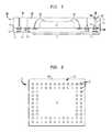
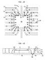
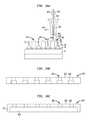
- FIG. 1shows a microelectronic package according to an embodiment of the present invention
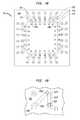
- FIG. 2shows a top elevation view of the microelectronic package of FIG. 1 ;
- FIG. 3shows a microelectronic package according to an alternative embodiment of the present invention
- FIG. 4shows a microelectronic package according to an alternative embodiment of the present invention
- FIG. 5shows a microelectronic package according to an alternative embodiment of the present invention
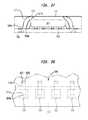
- FIG. 6shows a stacked microelectronic assembly including a microelectronic package according to an embodiment of the present invention
- FIG. 7shows a microelectronic package according to an alternative embodiment of the present invention.
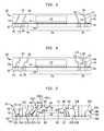
- FIGS. 8A-8Eshow a detail view of a portion of a microelectronic package according to various embodiments of the present invention.
- FIG. 9shows a detail view of a portion of a microelectronic package according to an alternative embodiment of the present invention.
- FIGS. 10A-10Dshow a detail view of a portion of a microelectronic package according to various embodiments of the present invention.
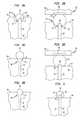
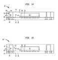
- FIGS. 11-14show a microelectronic package during various steps of fabrication thereof according to an embodiment of the present invention
- FIG. 15shows a microelectronic package during a fabrication step according to an alternative embodiment of the present invention.
- FIGS. 16A-16Cshow a detail view of a portion of a microelectronic package during various steps of fabrication thereof according to an embodiment of the present invention
- FIGS. 17A-17Cshow a detail view of a portion of a microelectronic package during various steps of fabrication thereof according to an alternative embodiment of the present invention
- FIG. 18shows a top elevation view of a microelectronic package according to an alternative embodiment of the present invention.
- FIG. 19shows a top elevation view of a portion of a microelectronic package according to an alternative embodiment of the present invention.
- FIG. 20shows a top view of a microelectronic package according to a further alternative embodiment of the present invention.
- FIG. 21shows a front elevation view of the microelectronic package of claim 20 ;
- FIG. 22shows a front elevation view of a microelectronic package according to a further alternative embodiment of the present invention.
- FIG. 23shows a system according to a further embodiment of the present invention.
- FIG. 24shows a front elevation view of a microelectronic package according to a further alternative embodiment of the present invention.
- FIG. 25shows a front elevation view of a microelectronic package according to a further alternative embodiment of the present invention.
- FIG. 26shows a top view of a microelectronic package according to a variation of the embodiment of FIG. 25 ;
- FIG. 27shows a front elevation view of a microelectronic package according to a further alternative embodiment of the present invention.
- FIG. 28shows a top view of a microelectronic package according to a variation of the embodiment of FIG. 27 ;
- FIG. 29is a sectional view of a microelectronic package according to a further embodiment.
- FIG. 30shows a sectional view of a microelectronic package according to another embodiment
- FIGS. 31A-Care sectional views showing examples of embodiments of microelectronic packages according to further embodiments.
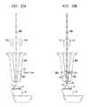
- FIGS. 32A and 32Bshow a portion of a machine that can be used in forming various wire bond vias in various stages of a method according to another embodiment of the present disclosure
- FIG. 33shows a portion of a machine that can be used in forming various wire bond vias according in a method according to another embodiment of the present disclosure.
- FIGS. 34A-Cshow various forms of an instrument that can be used in a method for making wire bonds according to an embodiment of the present disclosure.
- FIG. 1a microelectronic assembly 10 according to an embodiment of the present invention.
- the embodiment of FIG. 1is a microelectronic assembly in the form of a packaged microelectronic element such as a semiconductor chip assembly that is used in computer or other electronic applications.
- the microelectronic assembly 10 of FIG. 1includes a substrate 12 having a first surface 14 and a second surface 16 .
- the substrate 12typically is in the form of a dielectric element, which is substantially flat.
- the dielectric elementmay be sheet-like and may be thin.
- the dielectric elementcan include one or more layers of organic dielectric material or composite dielectric materials, such as, without limitation: polyimide, polytetrafluoroethylene (“PTFE”), epoxy, epoxy-glass, FR-4, BT resin, thermoplastic, or thermoset plastic materials.
- the first surface 14 and second surface 16are preferably substantially parallel to each other and are spaced apart at a distance perpendicular to the surfaces 14 , 16 defining the thickness of the substrate 12 .
- the thickness of substrate 12is preferably within a range of generally acceptable thicknesses for the present application.
- the distance between the first surface 14 and the second surface 16is between about 25 and 500 ⁇ m.
- the first surface 14may be described as being positioned opposite or remote from second surface 16 . Such a description, as well as any other description of the relative position of elements used herein that refers to a vertical or horizontal position of such elements is made for illustrative purposes only to correspond with the position of the elements within the Figures, and is not limiting.
- substrate 12is considered as divided into a first region 18 and a second region 20 .
- the first region 18lies within the second region 20 and includes a central portion of the substrate 12 and extends outwardly therefrom.
- the second region 20substantially surrounds the first region 18 and extends outwardly therefrom to the outer edges of the substrate 12 .
- no specific characteristic of the substrate itselfphysically divides the two regions; however, the regions are demarked for purposes of discussion herein with respect to treatments or features applied thereto or contained therein.
- a microelectronic element 22can be mounted to first surface 14 of substrate 12 within first region 18 .
- Microelectronic element 22can be a semiconductor chip or another comparable device.
- microelectronic element 22is mounted to first surface 14 in what is known as a conventional or “face-up” fashion.
- wire leads 24can be used to electrically connect microelectronic element 22 to some of a plurality of conductive elements 28 exposed at first surface 14 .
- Wire leads 24can also be joined to traces (not shown) or other conductive features within substrate 12 that are, in turn, connected to conductive elements 28 .
- Conductive elements 28include respective “contacts” or pads 30 that are exposed at the first surface 14 of substrate 12 .
- an electrically conductive elementwhen an electrically conductive element is described as being “exposed at” the surface of another element having dielectric structure, it indicates that the electrically conductive structure is available for contact with a theoretical point moving in a direction perpendicular to the surface of the dielectric structure toward the surface of the dielectric structure from outside the dielectric structure.
- a terminal or other conductive structure that is exposed at a surface of a dielectric structuremay project from such surface; may be flush with such surface; or may be recessed relative to such surface and exposed through a hole or depression in the dielectric.
- the conductive elements 28can be flat, thin elements in which pad 30 is exposed at first surface 14 of substrate 12 .
- conductive elements 28can be substantially circular and can be interconnected between each other or to microelectronic element 22 by traces (not shown).
- Conductive elements 28can be formed at least within second region 20 of substrate 12 . Additionally, in certain embodiments, conductive elements 28 can also be formed within first region 18 . Such an arrangement is particularly useful when mounting microelectronic element 122 ( FIG.
- microelectronic element 622is mounted face-down on substrate 612 and electrically connected to a conductive feature on the chip by wire leads 624 that extend over an outwardly-facing surface, such as surface 616 , of substrate 612 .
- wire leads 625pass through an opening 625 in substrate 612 and can be encapsulated by an overmold 699 .
- conductive elements 28are formed from a solid metal material such as copper, gold, nickel, or other materials that are acceptable for such an application, including various alloys including one or more of copper, gold, nickel or combinations thereof.
- conductive elements 28can be interconnected to corresponding second conductive elements 40 , such as conductive pads, exposed at second surface 16 of substrate 12 .
- Such an interconnectioncan be completed using vias 41 formed in substrate 12 that can be lined or filled with conductive metal that can be of the same material as conductive elements 28 and 40 .
- conductive elements 40can be further interconnected by traces on substrate 12 .
- Microelectronic assembly 10further includes a plurality of wire bonds 32 joined to at least some of the conductive elements 28 , such as on the pads 30 thereof.
- Wire bonds 32are joined at a base 34 thereof to the conductive elements 28 and can extend to a free end 36 remote from the respective bases 34 and from substrate 12 .
- the ends 36 of wire bonds 32are characterized as being free in that they are not electrically connected or otherwise joined to microelectronic element 22 or any other conductive features within microelectronic assembly 10 that are, in turn, connected to microelectronic element 22 .
- free ends 36are available for electronic connection, either directly or indirectly as through a solder ball or other features discussed herein, to a conductive feature external to assembly 10 .
- ends 36 held in a predetermined position by, for example, encapsulant layer 42 or otherwise joined or electrically connected to another conductive featuredoes not mean that they are not “free” as described herein, so long as any such feature is not electrically connected to microelectronic element 22 .
- base 34is not free as it is either directly or indirectly electrically connected to microelectronic element 22 , as described herein. As shown in FIG. 1 , base 34 can be substantially rounded in shape, extending outward from an edge surface 37 of wire bond 32 defined between base 34 and end 36 .
- base 34can vary according to the type of material used to form wire bond 32 , the desired strength of the connection between wire bond 32 and conductive element 28 , or the particular process used to form wire bond 32 .
- Exemplary methods for making wire bonds 28are described in U.S. Pat. No. 7,391,121 to Otremba and in U.S. Pat. App. Pub. No. 2005/0095835 (describing a wedge-bonding procedure that can be considered a form of wire bonding) the disclosures of which are both incorporated herein by reference in their entireties.
- Alternative embodimentsare possible where wire bonds 32 are additionally or alternatively joined to conductive elements 40 exposed on second surface 16 of substrate 12 , extending away therefrom.
- Wire bond 32can be made from a conductive material such as copper, gold, nickel, solder, aluminum or the like. Additionally, wire bonds 32 can be made from combinations of materials, such as from a core of a conductive material, such as copper or aluminum, for example, with a coating applied over the core. The coating can be of a second conductive material, such as aluminum, nickel or the like. Alternatively, the coating can be of an insulating material, such as an insulating jacket. In an embodiment, the wire used to form wire bonds 32 can have a thickness, i.e., in a dimension transverse to the wire's length, of between about 15 ⁇ m and 150 ⁇ m.
- wire bonds 32can have a thickness of up to about 500 ⁇ m.
- a wire bondis formed on a conductive element, such as conductive element 28 , a pad, trace or the like, using specialized equipment that is known in the art.
- a leading end of a wire segmentis heated and pressed against the receiving surface to which the wire segment bonds, typically forming a ball or ball-like base 34 joined to the surface of the conductive element 28 .
- the desired length of the wire segment to form the wire bondis drawn out of the bonding tool, which can then cut the wire bond at the desired length.
- Wedge bondingwhich can be used to form wire bonds of aluminum, for example, is a process in which the heated portion of the wire is dragged across the receiving surface to form a wedge that lies generally parallel to the surface. The wedge-bonded wire bond can then be bent upward, if necessary, and extended to the desired length or position before cutting.
- the wire used to form a wire bondcan be cylindrical in cross-section. Otherwise, the wire fed from the tool to form a wire bond or wedge-bonded wire bond may have a polygonal cross-section such as rectangular or trapezoidal, for example.
- the free end 36 of wire bond 32has an end surface 38 .
- End surface 38can form at least a part of a contact in an array formed by respective end surfaces 38 of a plurality of wire bonds 32 .
- FIG. 2shows an exemplary pattern for such an array of contacts formed by end surfaces 38 .
- Such an arraycan be formed in an area array configuration, variations of which could be implemented using the structures described herein.
- Such an arraycan be used to electrically and mechanically connect the microelectronic assembly 10 to another microelectronic structure, such as to a printed circuit board (“PCB”), or to other packaged microelectronic elements, an example of which is shown in FIG. 6 .
- PCBprinted circuit board
- wire bonds 32 and conductive elements 28 and 40can carry multiple electronic signals therethrough, each having a different signal potential to allow for different signals to be processed by different microelectronic elements in a single stack.
- Solder masses 52can be used to interconnect the microelectronic assemblies in such a stack, such as by electronically and mechanically attaching end surfaces 38 to conductive elements 40 .
- Microelectronic assembly 10further includes an encapsulation layer 42 formed from a dielectric material.
- encapsulation layer 42is formed over the portions of first surface 14 of substrate 12 that are not otherwise covered by or occupied by microelectronic element 22 , or conductive elements 28 .
- encapsulation layer 42is formed over the portions of conductive elements 28 , including pad thereof, that are not otherwise covered by wire bonds 32 .
- Encapsulation layer 42can also substantially cover microelectronic element 22 , wire bonds 32 , including the bases 34 and at least a portion of edge surfaces 37 thereof.
- a portion of wire bonds 32can remain uncovered by encapsulation layer 42 , which can also be referred to as unencapsulated, thereby making the wire bond available for electrical connection to a feature or element located outside of encapsulation layer 42 .
- end surfaces 38 of wire bonds 32remain uncovered by encapsulation layer 42 within major surface 44 of encapsulation layer 42 .
- Other embodimentsare possible in which a portion of edge surface 37 is uncovered by encapsulation layer 42 in addition to or as an alternative to having end surface 38 remain uncovered by encapsulation layer 42 .
- encapsulation layer 42can cover all of microelectronic assembly from first surface 14 and above, with the exception of a portion of wire bonds 36 , such as end surfaces 38 , edge surfaces 37 or combinations of the two.
- a surface, such as major surface 44 of encapsulation layer 42can be spaced apart from first surface 14 of substrate 12 at a distance great enough to cover microelectronic element 22 .
- embodiments of microelectronic assembly 10 in which ends 38 of wire bonds 32 are flush with surface 44will include wire bonds 32 that are taller than the microelectronic element 22 , and any underlying solder bumps for flip chip connection.
- Other configurations for encapsulation layer 42are possible.
- the encapsulation layercan have multiple surfaces with varying heights. In such a configuration, the surface 44 within which ends 38 are positioned can be higher or lower than an upwardly facing surface under which microelectronic element 22 is located.
- Encapsulation layer 42serves to protect the other elements within microelectronic assembly 10 , particularly wire bonds 32 . This allows for a more robust structure that is less likely to be damaged by testing thereof or during transportation or assembly to other microelectronic structures.
- Encapsulation layer 42can be formed from a dielectric material with insulating properties such as that described in U.S. Patent App. Pub. No. 2010/0232129, which is incorporated by reference herein in its entirety.
- FIG. 3shows an embodiment of microelectronic assembly 110 having wire bonds 132 with ends 136 that are not positioned directly above the respective bases 34 thereof. That is, considering first surface 114 of substrate 112 as extending in two lateral directions, so as to substantially define a plane, end 136 or at least one of the wire bonds 132 is displaced in at least one of these lateral directions from a corresponding lateral position of base 134 . As shown in FIG. 3 , wire bonds 132 can be substantially straight along the longitudinal axis thereof, as in the embodiment of FIG. 1 , with the longitudinal axis being angled at an angle 146 with respect to first surface 114 of substrate 112 . Although the cross-sectional view of FIG.
- wire bond 132can also be angled with respect to first surface 114 in another plane perpendicular to both that first plane and to first surface 114 .
- Such an anglecan be substantially equal to or different than angle 146 . That is the displacement of end 136 relative to base 134 can be in two lateral directions and can be by the same or a different distance in each of those directions.
- various ones of wire bonds 132can be displaced in different directions and by different amounts throughout the assembly 110 .
- Such an arrangementallows for assembly 110 to have an array that is configured differently on the level of surface 144 compared to on the level of substrate 12 .
- an arraycan cover a smaller overall area or have a smaller pitch on surface 144 than at the first surface 114 level compared to that at first surface 114 of substrate 112 .
- some wire bonds 132can have ends 136 that are positioned above microelectronic element 122 to accommodate a stacked arrangement of packaged microelectronic elements of different sizes. In another example, shown in FIG.
- wire bonds 132can be configured such that the end surface 138 A of one wire bond 132 A is positioned substantially above the base 134 B of another wire bond 1324 B, the end surface 138 B of that wire bond 132 B being positioned elsewhere.
- Such an arrangementcan be referred to as changing the relative position of a contact end surface 138 within an array of contacts, compared to the position of a corresponding contact array on second surface 116 .
- the relative positions of the contact end surfacescan be changed or varied, as desired, depending on the microelectronic assembly's application or other requirements.
- the wire bonds 132can be arranged such that the bases 134 are arranged in a first pattern having a pitch thereof.
- the wire bonds 132can be configured such that the unencapsulated portions thereof 139 , including end surfaces 138 can be disposed in a pattern at positions at a major surface 144 of the encapsulation layer 142 which have a minimum pitch that is greater than a minimum pitch between the respective adjacent bases 134 of the wire bonds attached to conductive elements 128 . Accordingly, the minimum pitch between adjacent wire bonds at the encapsulation surface 146 can be greater than the corresponding minimum pitch between the conductive elements 128 of the substrate to which the wire bonds are attached.
- the wire bondscan be angled, as shown in FIG. 30 , or can be curved as shown, for example in FIG. 4 , such that the end surfaces 138 are displaced in one or more lateral directions from the bases 134 , as discussed above.
- the conductive elements 128 and the end surfaces 138can be arranged in respective rows or columns and the lateral displacement of end surfaces 138 in one row can be greater than in another row.
- the wire bonds 132can, for example be at different angles 146 A, 146 B with respect to the surface 116 of the substrate 112 .
- FIG. 4shows a further embodiment of a microelectronic subassembly 210 having wire bonds 232 with ends 236 in displaced lateral positions with respect to bases 234 .
- the wire bonds 132achieve this lateral displacement by including a curved portion 248 therein.
- Curved portion 248can be formed in an additional step during the wire bond formation process and can occur, for example, while the wire portion is being drawn out to the desired length. This step can be carried out using available wire-bonding equipment, which can include the use of a single machine.
- Curved portion 248can take on a variety of shapes, as needed, to achieve the desired positions of the ends 236 of the wire bonds 232 .
- curved portions 248can be formed as S-curves of various shapes, such as that which is shown in FIG. 4 or of a smoother form (such as that which is shown in FIG. 5 ). Additionally, curved portion 248 can be positioned closer to base 234 than to end 236 or vice-versa. Curved portion 248 can also be in the form of a spiral or loop, or can be compound including curves in multiple directions or of different shapes or characters.
- FIG. 5shows a further exemplary embodiment of a microelectronic package 310 having a combination of wire bonds 332 having various shapes leading to various relative lateral displacements between bases 334 and ends 336 .
- Some of wire bonds 332 Aare substantially straight with ends 336 A positioned above their respective bases 334 A, while other wire bonds 332 B include a subtle curved portion 348 B leading to a somewhat slight relative lateral displacement between end 336 B and base 334 B.
- some wire bonds 332 Cinclude curved portions 348 C having a sweeping shape that result in ends 336 C that are laterally displaced from the relative bases 334 C at a greater distance than that of ends 334 B.
- 5also shows an exemplary pair of such wire bonds 332 Ci and 332 Cii that have bases 334 Ci and 334 Cii positioned in the same row of a substrate-level array and ends 336 Ci and 336 Cii that are positioned in different rows of a corresponding surface-level array.
- a further variation of a wire bond 332 Dis shown that is configured to be uncovered by encapsulation layer 342 on a side surface 47 thereof.
- free end 336 Dis uncovered, however, a portion of edge surface 337 D can additionally or alternatively be uncovered by encapsulation layer 342 .
- Such a configurationcan be used for grounding of microelectronic assembly 10 by electrical connection to an appropriate feature or for mechanical or electrical connection to other featured disposed laterally to microelectronic assembly 310 .
- FIG. 5shows an area of encapsulation layer 342 that has been etched away, molded, or otherwise formed to define a recessed surface 345 that is positioned closer to substrate 12 than major surface 342 .
- wire bond 332 Acan be uncovered within an area along recessed surface 345 .
- end surface 338 A and a portion of edge surface 337 Aare uncovered by encapsulation layer 342 .
- Such a configurationcan provide a connection, such as by a solder ball or the like, to another conductive element by allowing the solder to wick along edge surface 337 A and join thereto in addition to joining to end surface 338 .
- FIG. 5further shows a microelectronic assembly 310 having two microelectronic elements 322 and 350 in an exemplary arrangement where microelectronic element 350 is stacked, face-up, on microelectronic element 322 .
- leads 324are used to electrically connect microelectronic element 322 to conductive features on substrate 312 .
- Various leadsare used to electronically connect microelectronic element 350 to various other features of microelectronic assembly 310 .
- lead 380electrically connects microelectronic element 350 to conductive features of substrate 312
- lead 382electrically connects microelectronic element 350 to microelectronic element 322 .
- wire bond 384which can be similar in structure to various ones of wire bonds 332 , is used to form a contact surface 386 on the surface 344 of encapsulation layer 342 that electrically connected to microelectronic element 350 .
- Thiscan be used to directly electrically connect a feature of another microelectronic assembly to microelectronic element 350 from above encapsulation layer 342 .
- Such a leadcould also be included that is connected to microelectronic element 322 , including when such a microelectronic element is present without a second microelectronic element 350 affixed thereon.
- An openingcan be formed in encapsulation layer 342 that extends from surface 344 thereof to a point along, for example, lead 380 , thereby providing access to lead 380 for electrical connection thereto by an element located outside surface 344 .
- a similar openingcan be formed over any of the other leads or wire bonds 332 , such as over wire bonds 332 C at a point away from the ends 336 C thereof.
- ends 336 Ccan be positioned beneath surface 344 , with the opening providing the only access for electrical connection thereto.
- FIG. 6shows a stacked package of microelectronic assemblies 410 and 488 .
- solder masses 452electrically and mechanically connect end surfaces 438 of assembly 410 to conductive elements 440 of assembly 488 .
- the stacked packagecan include additional assemblies and can be ultimately attached to contacts 492 on a PCB 490 or the like for use in an electronic device.
- wire bonds 432 and conductive elements 430can carry multiple electronic signals therethrough, each having a different signal potential to allow for different signals to be processed by different microelectronic elements, such as microelectronic element 422 or microelectronic element 489 , in a single stack.
- wire bonds 432are configured with a curved portion 448 such that at least some of the ends 436 of the wire bonds 432 extend into an area that overlies a major surface 424 of the microelectronic element 422 .
- Such an areacan be defined by the outer periphery of microelectronic element 422 and extending upwardly therefrom.
- An example of such a configurationis shown from a view facing toward first surface 414 of substrate 412 in FIG. 18 , where wire bonds 432 overlie a rear major surface of the microelectronic element 422 , which is flip-chip bonded at a front face 425 thereof to substrate 412 .
- FIG. 18In another configuration ( FIG.
- the microelectronic element 422can be mounted face-up to the substrate 312 , with the front face 325 facing away from the substrate 312 and at least one wire bond 336 overlying the front face of microelectronic element 322 .
- wire bond 336is not electrically connected with microelectronic element 322 .
- a wire bond 336 bonded to substrate 312may also overlie the front or rear face of microelectronic element 350 .
- conductive elements 428are arranged in a pattern forming a first array in which the conductive elements 428 are arranged in rows and columns surrounding microelectronic element 422 and may have a predetermined pitch between individual conductive elements 428 .
- Wire bonds 432are joined to the conductive elements 428 such that the respective bases 434 thereof follow the pattern of the first array as set out by the conductive elements 428 .
- Wire bonds 432are configured, however, such that the respective ends 436 thereof can be arranged in a different pattern according to a second array configuration. In the embodiment shown the pitch of the second array can be different from, and in some cases finer than that of the first array.
- conductive elements 428can be configured in sets of arrays positioned throughout substrate 412 and wire bonds 432 can be configured such that ends 436 are in different sets of arrays or in a single array.
- FIG. 6further shows an insulating layer 421 extending along a surface of microelectronic element 422 .
- Insulating layer 421can be formed from a dielectric or other electrically insulating material prior to forming the wire bonds.
- the insulating layer 421can protect microelectronic element from coming into contact with any of wire bonds 423 that extend thereover.
- insulating layer 421can avoid electrical short-circuiting between wire bonds and short-circuiting between a wire bond and the microelectronic element 422 . In this way, the insulating layer 421 can help avoid malfunction or possible damage due to unintended electrical contact between a wire bond 432 and the microelectronic element 422 .
- microelectronic assembly 410can connect to another microelectronic assembly, such as microelectronic assembly 488 , in certain instances where the relative sizes of, for example, microelectronic assembly 488 and microelectronic element 422 would not otherwise permit.
- microelectronic assembly 488is sized such that some of the contact pads 440 are in an array within an area smaller than the area of the front or rear surface 424 or 426 of the microelectronic element 422 .
- substantially vertical conductive features, such as pillarsin place of wire bonds 432 , direct connection between conductive elements 428 and pads 440 would not be possible.
- wire bonds 432 having appropriately-configured curved portions 448can have ends 436 in the appropriate positions to make the necessary electronic connections between microelectronic assembly 410 and microelectronic assembly 488 .
- Such an arrangementcan be used to make a stacked package where microelectronic assembly 418 is, for example, a DRAM chip or the like having a predetermined pad array, and wherein microelectronic element 422 is a logic chip configured to control the DRAM chip.
- microelectronic element 422is a logic chip configured to control the DRAM chip.
- Thiscan allow a single type of DRAM chip to be used with several different logic chips of varying sizes, including those which are larger than the DRAM chip because the wire bonds 432 can have ends 436 positioned wherever necessary to make the desired connections with the DRAM chip.
- microelectronic package 410can be mounted on printed circuit board 490 in another configuration, where the unencapsulated surfaces 436 of wire bonds 432 are electrically connected to pads 492 of circuit board 490 .
- another microelectronic packagesuch as a modified version of package 488 can be mounted on package 410 by solder balls 452 joined to pads 440 .
- FIGS. 31A-CAdditional arrangements for microelectronic packages having multiple microelectronic elements are shown in FIGS. 31A-C . These arrangements can be used in connection with the wire bond arrangements shown, for example in FIG. 5 and in the stacked package arrangement of FIG. 6 , discussed further below.
- FIG. 31Ashows an arrangement in which a lower microelectronic element 1622 is flip-chip bonded to conductive elements 1628 on the surface 1614 of substrate 1612 .
- the second microelectronic element 1650is face-up mounted on top of the first microelectronic element 1622 and connected through wire bonds 1688 to additional conductive elements 1628 .
- FIG. 31Ashows an arrangement in which a lower microelectronic element 1622 is flip-chip bonded to conductive elements 1628 on the surface 1614 of substrate 1612 .
- the second microelectronic element 1650is face-up mounted on top of the first microelectronic element 1622 and connected through wire bonds 1688 to additional conductive elements 1628
- FIG. 31Bshows an arrangement where a first microelectronic element 1722 is face-up mounted on surface 1714 and connected through wire bonds 1788 to conductive elements 1728 .
- Second microelectronic element 1750is flip-chip mounted on top of first microelectronic element 1722 through a set of contacts 1726 of the second microelectronic element 1750 which face and are joined to corresponding contacts on the front face of the first microelectronic element 1722 .
- These contacts on the first microelectronic element 1722in turn can be connected through circuit patterns of the first microelectronic element 1722 and be connected by some of the ire bonds 1788 to the conductive elements 1728 on substrate 1712 .
- FIG. 31Cshows an arrangement where first 1822 and second 1850 microelectronic elements are mounted side-by-side on surface 1814 of substrate 1812 .
- Either one or both of the microelectronic elements (and additional microelectronic elements)can be mounted in the face-up or flip-chip configurations described herein.
- any of the microelectronic elements employed in such an arrangementcan be connected to each other through circuit patterns on one or both such microelectronic elements or on the substrate or on both, which electrically connect respective conductive elements 1828 to which the microelectronic elements are electrically connected.
- FIG. 7shows a microelectronic assembly 10 , of the type shown in FIG. 1 with a redistribution layer 54 extending along surface 44 of encapsulation layer 42 .
- traces 58are electrically connected to inner contact pads 61 which are electrically connected to end surfaces 38 of wire bonds 32 and extend through the substrate 56 of redistribution layer 54 to contact pads 60 exposed on surface 62 of substrate 56 .
- An additional microelectronic assemblycan then be connected to contact pads 60 by solder masses or the like.
- a similar structure to redistribution layer 54can extend along second surface 16 of substrate 12 in what is known as a fan-out layer.
- a fan-out layercan allow microelectronic assembly 10 to connect to an array of a different configuration than the conductive element 40 array would otherwise permit.
- FIGS. 8A-8Eshow various configurations that can be implemented in the structure of or near the ends 36 of wire bonds 32 in a structure similar to FIGS. 1-7 .
- FIG. 8Ashows a structure in which a cavity 64 is formed in a portion of encapsulation layer 42 such that an end 36 of wire bond 32 projects above a minor surface 43 of the encapsulation layer at cavity 64 .
- end surface 38is positioned below major surface 44 of encapsulation layer 42
- cavity 64is structured to expose end surface 38 at surface 44 to allow an electronic structure to connect thereto.
- Other embodimentsare possible wherein end surface 38 is substantially even with surface 44 or is spaced above surface 44 .
- cavity 64can be configured such that a portion of edge surface 37 of wire bond 32 near the end 36 thereof can be uncovered by encapsulation layer 42 within cavity 64 . This can allow for a connection to wire bond 32 from outside of assembly 10 , such as a solder connection, to be made from both end surface 38 and the uncovered portion of edge surface 37 near end 36 . Such a connection is shown in FIG. 8B and can provide a more robust connection to a second substrate 94 using a solder mass 52 .
- cavity 64can have a depth beneath surface 44 of between about 10 ⁇ m and 50 ⁇ m and can have a width of between about 100 ⁇ m and 300 ⁇ m.
- FIG. 8Bshows a cavity having a similar structure to that of FIG.
- FIG. 8Bshows a second microelectronic assembly 94 electrically and mechanically connected to wire bond 32 by a solder mass 52 at a contact pad 96 exposed at a surface of a substrate 98 thereof.
- Cavity 64can be formed by removing a portion of encapsulation layer 42 in the desired area of cavity 64 . This can be done by known processes including, laser etching, wet etching, lapping or the like. Alternatively, in an embodiment where encapsulation layer 42 is formed by injection molding, cavity 64 can be formed by including a corresponding feature in the mold. Such a process is discussed in U.S. Pat. App. Pub. No. 2010/0232129, which is hereby incorporated by reference in its entirety. The tapered shape of cavity 64 shown in FIG. 8B can be the result of a particular etching process used in its formation.
- FIGS. 8C and 8Eshow end structures that include a substantially rounded end portion 70 on wire bond 32 .
- Rounded end portion 70is configured to have a cross-section that is wider than the cross-section of the portion of wire bond 32 between base 34 and end 36 .
- Further rounded end portion 70includes an edge surface 71 that extends outward from the edge surface 37 of wire bond 32 at the transition therebetween.
- the incorporation of a rounded edge portion 70can act to secure wire bond 32 within encapsulation layer 42 by providing an anchoring feature wherein the change in direction of the surface 71 gives encapsulation layer 42 a location to surround end 70 on three sides. This can help prevent wire bond 32 from becoming detached from conductive elements 28 on substrate 12 , resulting in a failed electrical connection.
- the rounded end portion 70can provide increased surface area that is uncovered by encapsulation layer 42 within surface 44 to which an electronic connection can be made. As shown in FIG. 8E , rounded end portion 70 can extend above surface 44 . Alternatively, as shown in FIG. 8C , rounded end portion 70 can further, be ground or otherwise flattened to provide a surface that is substantially flush with surface 44 and can have an area greater than the cross-section of wire bond 32 .
- a rounded end portion 70can be formed by applying localized heat in the form of a flame or a spark at the end of the wire used to make wire bond 32 .
- Known wire bonding machinescan be modified to carry out this step, which can be done immediately after cutting the wire. In this process, the heat melts the wire at the end thereof. This localized portion of liquid metal is made round by the surface tension thereof and is retained when the metal cools.
- FIG. 8Dshows a configuration for microelectronic assembly 10 where end 36 of wire bond 32 includes a surface 38 that is spaced above major surface 44 of encapsulation layer 42 .
- Such a configurationcan present benefits similar to that discussed with respect to cavity 64 , above, specifically, by providing a more robust connection with a solder mass 68 that wicks along the portion of edge surface 37 that is uncovered by encapsulation layer 42 above surface 44 .
- end surface 38can be spaced above surface 42 at a distance of between about 10 ⁇ m and 50 ⁇ m. Additionally, in the embodiment of FIG.
- the endcan include a protective layer formed thereon.
- a protective layercan include an oxidation protection layer, including those made from gold, an oxide coating or an OSP.
- FIG. 9shows an embodiment of microelectronic assembly 10 with a stud bump 72 formed on end surface 38 of wire bond 32 .
- Stud bump 72can be formed after making microelectronic assembly 10 by applying another, modified wire bond on top of end surface 44 and optionally extending along a portion of surface 44 . The modified wire bond is cut or otherwise severed near the base thereof without drawing out a length of wire.
- Stud bumps 72 containing certain metalsmay be applied directly to ends 38 without first applying a bonding layer such as a UBM, thus providing way of forming conductive interconnects to bond pads which are not directly wettable by solder. This can be useful when wire bond 32 is made from a non-wettable metal.
- stud bumpsconsisting essentially of one or more of copper, nickel, silver, platinum and gold can be applied this way.
- FIG. 9shows a solder mass 68 formed over stud bump 72 for electronic or mechanical connection to an additional microelectronic assembly.
- FIGS. 10A-10Dshow configurations for ends 36 of wire bonds 32 that include a bent or curved shape.
- end 36 of wire bond 32is bent such that a portion thereof extends substantially parallel to surface 44 of encapsulation layer 42 such that at least a portion of edge surface 76 is not covered by, for example, major surface 44 .
- This portion of edge surface 37can extend upwards outside of surface 44 or can be ground or otherwise flattened so as to extend substantially flush with surface 44 .
- the embodiment of FIG. 10Aincludes an abrupt bend in wire bond 32 at the portion 74 of end 36 that is parallel to surface 44 and terminates in an end surface 38 that is substantially perpendicular to surface 44 .
- FIG. 10Aincludes an abrupt bend in wire bond 32 at the portion 74 of end 36 that is parallel to surface 44 and terminates in an end surface 38 that is substantially perpendicular to surface 44 .
- FIG. 10Bshows an end 36 having a more gradual curve near the portion 74 of end 36 that is parallel to surface 44 than that which is shown in FIG. 10A .
- Other configurationsare possible, including those in which a portion of a wire bond according to those shown in FIG. 3 , 4 , or 5 includes an end with a portion thereof substantially parallel to surface 44 and having a portion of the edge surface thereof uncovered by encapsulation layer 42 at a location within surface 44 .
- the embodiment of FIG. 10Bincludes a hooked portion 75 on the end thereof, which positions end surface 38 below surface 44 within encapsulation layer 42 . This can provide a more robust structure for end 36 that is less likely to become dislodged from within encapsulation layer 42 .
- 10C and 10Dshow structures that are, respectively, similar to those shown in FIGS. 10A and 10B , but are uncovered by encapsulation layer 42 at a location along surface 44 by cavities 64 formed in encapsulation layer 42 . These cavities can be similar in structure to those discussed above with respect to FIGS. 8A and 8B .
- the inclusion of ends 36 including a portion 74 thereof that extends parallel to surface 44can provide increased surface area for connection therewith by virtue of the elongated uncovered edge surface 75 .
- the length of such a portion 74can be greater than the width of cross-section of the wire used to form wire bond 32 .
- multiple wire bonds 1432can be joined on a single conductive element 1428 .
- Such a group of wire bonds 1432can be used to make additional connection points over the encapsulation layer 1442 for electrical connection with conductive element 1428 .
- the exposed portions 1439 of the commonly-joined wire bonds 1432can be grouped together on surface 1444 of encapsulation layer 1442 in an area, for example about the size of conductive element 1428 itself or another area approximating the intended size of a bonding mass for making an external connection with the wire bond 1432 group.
- Such wire bonds 1432can be either ball-bonded, as shown, or edge bonded on conductive element 1428 , as described above.
- the various techniques described herein for severing the metal wire during the wire bonding processe.g., by laser or other cutting instrument can be employed when forming multiple wire bonds to a conductive element on a substrate.
- FIGS. 11-15show a microelectronic assembly 10 in various steps of a fabrication method thereof.
- FIG. 11shows microelectronic assembly 10 ′ at a step where microelectronic element 22 has been electrically and mechanically connected to substrate 12 on first surface 14 and within first region 18 , thereof.
- Microelectronic element 22is shown in FIG. 11 as being mounted on substrate 12 in a flip-chip arrangement, such as through contacts on microelectronic element 22 which face and are joined to corresponding contacts on a confronting surface 14 of the substrate.
- the joints between the contacts of the microelectronic element and the substratecan be made through electrically conductive material such as masses 26 , e.g., a conductive paste, conductive matrix material, solder masses, and the contacts can be of any suitable configuration such as pads, posts, e.g., micropillars, stud bumps, etc., among others.
- electrically conductive materialsuch as masses 26 , e.g., a conductive paste, conductive matrix material, solder masses
- the contactscan be of any suitable configuration such as pads, posts, e.g., micropillars, stud bumps, etc., among others.
- Flip-chip bondingis used herein to mean such arrangement of face-to-face electrical bonding between corresponding contacts of a microelectronic element and a substrate, or between a microelectronic element and another microelectronic element.
- a dielectric underfill layer 66may be provided between microelectronic element 22 and substrate 12 .
- FIG. 12shows microelectronic assembly 10 ′′ having wire bonds 32 applied on pads 30 of conductive elements 28 exposed on first surface 14 of substrate 12 .
- wire bonds 32can be applied by heating an end of a wire segment to soften the end such that it forms a deposition bond to conductive element 28 when pressed thereto, forming base 34 . The wire is then drawn out away from conductive element 28 and manipulated, if desired, in a specified shape before being cut or otherwise severed to form end 36 and end surface 38 of wire bond 32 .
- wire bonds 32can be formed from, for example, an aluminum wire by wedge bonding. Wedge-bonding is formed by heating a portion of the wire adjacent the end thereof and dragging it along the conductive element 28 with pressure applied thereto. Such a process is described further in U.S. Pat. No. 7,391,121, the disclosure of which is hereby incorporated by reference herein in its entirety.
- encapsulation layer 42has been added to microelectronic assembly 10 ′′′ by being applied over first surface 14 of substrate, extending upwardly therefrom and along edge surfaces 37 of wire bonds 32 .
- Encapsulation layer 42also covers underfill layer 66 .
- Encapsulation layer 42can be formed by depositing a resin over microelectronic assembly 10 ′′ shown in FIG. 12 . This can be done by placing assembly 10 ′′ in an appropriately configured mold having a cavity in the desired shape of the encapsulation layer 42 that can receive assembly 10 ′.
- Such a mold and the method of forming an encapsulation layer therewithcan be as shown and described in U.S. Pat. App. Pub. No 2010/0232129, the disclosure of which is incorporated by reference herein it its entirety.
- encapsulation layer 42can be prefabricated to the desired shape from an at least partially compliant material.
- compliant properties of the dielectric materialallow encapsulation layer 42 to be pressed into position over wire bonds 32 and microelectronic element 22 .
- wire bonds 32penetrate into the compliant material forming respective holes therein, along which encapsulation layer 42 contacts edge surfaces 37 .
- microelectronic element 22may deform the compliant material so that it can be received therein.
- the compliant dielectric materialcan be compressed to expose end surfaces 38 on outer surface 44 .
- any excess compliant dielectric materialcan be removed from encapsulation layer to form a surface 44 on which ends surfaces 38 of wire bonds 32 are uncovered or cavities 64 can be formed that uncover end surfaces 38 at a location within surface 63 .
- encapsulation layeris formed such that, initially, surface 44 thereof is spaced above end surfaces 38 of wire bonds 32 .
- the portion of encapsulation layer 42 that is above end surfaces 38can be removed, exposing a new surface 44 ′ that is substantially flush with end surfaces 42 , as shown in FIG. 14 .
- cavities 64such as those shown in FIGS. 8A and 8 B can be formed in which end surfaces 38 are uncovered by encapsulation layer 42 .
- encapsulation layer 42can be formed such that surface 44 is already substantially flush with end surfaces 48 or such that surface 44 is positioned below end surfaces 48 , as shown in FIG. 8D .
- Removal, if necessary, of a portion of encapsulation layer 42can be achieved by grinding, dry etching, laser etching, wet etching, lapping, or the like. If desired, a portion of the ends 36 of wire bonds 32 can also be removed in the same, or an additional, step to achieve substantially planar end surface 38 that are substantially flush with surface 44 . If desired, cavities 64 can also be formed after such a step, or stud bumps, as shown in FIG. 10 can also be applied. The resulting microelectronic assembly 10 can then be affixed on a PCB or otherwise incorporated in a further assembly, for example a stacked package, as shown in FIG. 6 .
- wire bonds 32are initially formed in pairs as portions 32 ′ of a wire loop 86 .
- loop 86is made in the form of a wire bond as discussed above.
- the wire segmentis drawn upward, then bent and drawn in a direction having at least a component thereof in the direction of the first surface 14 of substrate 13 and to a position substantially overlying an adjacent conductive element 28 .
- the wireis then drawn substantially downward to a position near the adjacent conductive element 28 before being cut or otherwise severed.
- the wireis then heated and connected to the adjacent conductive element 28 by deposition bonding or the like to form loop 86 .
- Encapsulation layer 42is then formed so as to substantially cover loop 86 .
- a portion of encapsulation layer 42is then removed by grinding, etching or the like by a process that also removes a portion of loop 86 such that the loop is severed and divided into its two portions 32 ′, thereby forming wire bonds 32 with end surfaces 38 uncovered by encapsulation layer 42 at a location along surface 44 which is formed on encapsulation layer 42 . Subsequent finishing steps can then be applied to assembly 10 , as discussed above.
- FIGS. 16A-16Cshow steps in an alternative embodiment for making cavities 64 , as discussed above, surrounding ends 36 of wire bonds 32 .
- FIG. 16Ashows a wire bond 32 , of the general type discussed above with respect to FIGS. 1-6 .
- Wire bond 32has a mass of sacrificial material 78 applied on end 36 thereof.
- the sacrificial material mass 78can be substantially spherical in shape, which can result from the material's surface tension during formation thereof, or other desired shapes that would be understood by a person of ordinary skill in the art.
- Sacrificial material mass 78can be formed by dipping the ends 36 of wire bonds 32 in solder paste to coat the ends thereof.
- the viscosity of the solder pastecan be adjusted prior to dipping to control the amount of solder mass that wicking and surface tension cause to adhere to ends 36 . This can, accordingly, affect the size of masses 78 that are applied on ends 36 .
- masses 78can be formed by depositing a soluble material onto the ends 36 of the wire bonds 32 .
- Other possible masses 78can be individual solder balls or other masses on ends or by other means using other materials, such as copper or gold flashing, used in microelectronic component fabrication, that can later be removed.
- a dielectric layer 42is shown having been added to assembly 10 , including upward along edge surfaces 37 of wire bonds 32 .
- the dielectric layeralso extends along a portion of the surface of the sacrificial material mass 78 , such that it is spaced apart from the end 36 of the wire bond 32 thereby.
- sacrificial material mass 78is removed, such as by washing or rinsing in a solvent, melting, chemical etching or other technique, leaving cavity 64 in dielectric layer 42 substantially in the negative shape of mass 78 before removal thereof, and exposing a portion of edge surface 37 near end 36 of wire bond 32 .
- sacrificial material mass 78can be formed to coat substantially all of wire bond 32 by extending along the edge surface 37 thereof. This arrangement is shown in FIG. 17A . Such a coating can be applied over wire bonds 32 after formation on assembly 10 , as discussed above, or can be applied as a coating to the wire used to make wire bonds 32 . This would, essentially, be in the form or a coated wire or a two-part wire, for example, with an inner core of copper and a solder coating.
- FIG. 17Bshows dielectric layer 42 applied over wire bonds 32 and the sacrificial mass 78 so as to extend along the edge surface 79 of the sacrificial mass 78 , thereby spacing apart dielectric layer 42 from wire bond 32 substantially along the length thereof.
- FIG. 17Cshows the structure that results from removing a portion of the sacrificial material mass 78 to form cavity 64 around end 36 and exposing a portion of edge surface 37 .
- a majority of, or at least a portion of, the sacrificial material mass 78can be left in place between dielectric layer 42 and wire bond 32 .
- FIG. 17Cfurther shows a solder mass 52 electrically and mechanically connecting wire bond 32 to a contact pad 40 A of another microelectronic structure 10 A.
- the wire bond( 32 in FIG. 1 , for example) is then separated from a remaining portion of the wire within the capillary (such as 804 in FIG. 32 ). This can be done at any location remote from the base 34 of the wire bond 32 and is preferably done at a location remote from the base 34 by a distance at least sufficient to define the desired height of the wire bond 32 . Such separation can be carried out by a mechanism disposed within the capillary 804 or disposed outside of the capillary 804 , between the face 806 and the base 34 of the wire bond 32 .
- the wire segment 800can be separated by effectively burning through the wire 800 at the desired separation point, which can be done by application of a spark or flame thereto.
- different forms of cutting the wire segment 800can be implemented. As described herein, cutting can be used to describe a partial cut that can weaken the wire at a desired location or cutting completely through the wire for total separation of the wire bond 32 from the remaining wire segment 800 .
- a cutting blade 805can be integrated into the bond head assembly, such as within capillary 804 .
- an opening 807can be included in the side wall 820 of the capillary 804 through which cutting blade 805 can extend.
- the cutting blade 805can be moveable in and out of the interior of the capillary 804 so that it can alternately allow the wire 800 to freely pass therethrough or engage the wire 800 .
- the wire 800can be drawn out and the wire bond 32 formed and bonded to a conductive element 28 with the cutting blade 805 in a position outside of the capillary interior.
- the wire segment 800can be clamped using a clamp 803 integrated in the bond head assembly to secure the position of the wire.
- the cutting blade 803can then be moved into the wire segment to either fully cut the wire or to partially cut or weaken the wire.
- a full cutcan form end surface 38 of the wire bond 32 at which point the capillary 804 can be moved away from the wire bond 32 to, for example, form another wire bond.
- the wire segment 800is weakened by the cutting blade 805 , movement of the bond head unit with the wire still held by the wire clamp 803 can cause separation by breaking the wire 800 at the area weakened by the partial cut.
- the movement of the cutting blade 805can be actuated by pneumatics or by a servo motor using an offset cam. In other examples the cutting blade 805 movement can be actuated by a spring or a diaphragm.
- the triggering signal for the cutting blade 805 actuationcan be based on a time delay that counts down from formation of the ball bond or can be actuated by movement of the capillary 804 to a predetermined height above the wire bond base 34 . Such a signal can be linked to other software that operates the bonding machine so that the cutting blade 805 position can be reset prior to any subsequent bond formation.
- the cutting mechanismcan also include a second blade (not shown) spaced opposite blade 805 to cut the wire from opposing sides thereof.
- a laser 809can be assembled with the bond head unit and positioned to cut the wire segment.
- a laser head 809can be positioned outside of capillary 804 such as by mounting thereto or to another point on the bond head unit that includes capillary 804 .
- the lasercan be actuated at a desired time, such as those discussed above with respect to the cutting blade 805 in FIG. 32 , to cut the wire 800 , forming end surface 38 of the wire bond 32 at a desired height above the base 34 .
- the laser 809can be positioned to direct the cutting beam through or into the capillary 804 itself and can be internal to the bond head unit.
- a carbon dioxide lasercan be used or, as an alternative, a Nd:YAG or a Cu vapor laser could be used.
- a stencil 824 as shown in FIGS. 34A-Ccan be used to separate the wire bonds 32 from the remaining wire segment 800 .
- the stencil 824can be a structure having a body that defines an upper surface 826 at or near the desired height of the wire bonds 32 .
- the stencil 824can be configured to contact the conductive elements 28 or any portions of the substrate 12 between the conductive elements 28 .
- the stencilincludes a plurality of holes 828 that can correspond to the desired locations for the wire bonds 32 , such as over conductive elements 28 .
- the holes 828can be sized to accept the capillary 804 of the bond head unit therein so that the capillary can extend into the hole to a position relative to the conductive element 28 to bond the wire 800 to the conductive element, 28 to form the base 34 , such as by ball bonding or the like.
- the capillary 804can then be moved vertically out of the hole 828 while drawing out the wire segment to a desired length.
- the wire segmentcan be clamped within the bond head unit, such as by clamp 803 , and the capillary 804 can be moved in a lateral direction (such as parallel to the surface 826 of stencil 824 ) to move the wire segment 800 into contact with an edge 829 of the stencil 824 defined by the intersection of the surface of the hole 828 and the outside surface 826 of the stencil 824 .
- Such movementcan cause separation of the wire bond 32 from a remaining portion of the wire segment 800 that is still held within the capillary 804 . This process can be repeated to form the desired number of wire bonds 32 in the desired locations.
- the capillarycan be moved vertically prior to wire separation such that the remaining wire segment projects beyond the face 806 of the capillary 804 by a distance 802 sufficient to form a subsequent ball bond.
- FIG. 34Bshows a variation of stencil 824 in which the holes 828 are tapered such that they have a diameter that increases from a first diameter at surface 826 to a greater diameter away from surface 826 .
- the stencilcan be formed having an outer frame 821 having a thickness sufficient to space apart surface 826 at the desired distance from substrate 12 .
- Frame 821can at least partially surround a cavity 823 configured to be positioned adjacent substrate 12 with a thickness of the stencil 824 extending between the surface 826 and the open area 823 such that the portion of stencil 824 that includes the holes 828 is spaced apart from the substrate 12 when positioned thereon.
- FIGS. 20 and 21show a further embodiment of a microelectronic assembly 510 in which wire bonds 532 are formed on a lead-frame structure.
- lead frame structuresare shown and described in U.S. Pat. Nos. 7,176,506 and 6,765,287 the disclosures of which are hereby incorporated by reference herein.
- a lead frameis a structure formed from a sheet of conductive metal, such as copper, that is patterned into segments including a plurality of leads and can further include a paddle, and a frame. The frame is used to secure the leads and the paddle, if used, during fabrication of the assembly.
- a microelectronic elementsuch as a die or chip
- the microelectronic elementcan be joined face-up to the paddle and electrically connected to the leads using wire bonds.
- the microelectronic elementcan be mounted directly onto the leads, which can extend under the microelectronic element.
- contacts on the microelectronic elementcan be electrically connected to respective leads by solder balls or the like.
- the leadscan then be used to form electrical connections to various other conductive structures for carrying an electronic signal potential to and from the microelectronic element.
- temporary elements of the framecan be removed from the leads and paddle of the lead frame, so as to form individual leads.
- the individual leads 513 and the paddle 515are considered to be segmented portions of what, collectively, forms a substrate 512 that includes conductive elements 528 in portions that are integrally formed therewith. Further, in this embodiment, paddle 515 is considered to be within first region 518 of substrate 512 , and leads 513 are considered to be within second region 520 .
- Wire bonds 524which are also shown in the elevation view of FIG. 21 , connect microelectronic element 22 , which is carried on paddle 515 , to conductive elements 528 of leads 515 . Wire bonds 532 can be further joined at bases 534 thereof to additional conductive elements 528 on leads 515 .
- Encapsulation layer 542is formed onto assembly 510 leaving ends 538 of wire bonds 532 uncovered at locations within surface 544 .
- Wire bonds 532can have additional or alternative portions thereof uncovered by encapsulation layer 542 in structures that correspond to those described with respect to the other embodiments herein.
- FIGS. 24-26show a further alternative embodiment of a microelectronic package 810 having closed-loop wire bonds 832 .
- the wire bonds 832 of this embodimentinclude two bases 834 a and 834 b that can be joined to adjacent conductive elements 828 a and 828 b , as shown in FIG. 24 .
- the bases 834 a , 834 bcan both be joined on a common conductive element 828 , as shown in FIGS. 25 and 26 .
- wire bonds 832define an edge surface 837 that extends between the two bases 834 a , 834 b in a loop such that the edge surface 837 extends upward in respective portions 837 a and 837 b from the bases to an apex 839 at a surface 844 of the encapsulation layer 842 above the substrate 812 .
- Encapsulation layer 842extends along at least some of edge surface portions 837 a , 837 b , separating the respective portions from one another, as well as from other wire bonds 832 in package 810 .
- apex 839At least a portion of the edge surface 837 is uncovered by the encapsulation layer 842 , such that the wire bond 832 is available for electrical interconnection with another component, which can be another microelectronic component or other component, e.g., a discrete element such as a capacitor or inductor.
- wire bonds 832are formed such that apex 839 is offset from conductive element 828 in at least one lateral direction across the surface of the substrate 812 .
- apex 839can overlie a major surface of microelectronic element 820 or otherwise overlie a first region of the substrate 812 with which the microelectronic element 820 is aligned.
- wire bonds 832are possible, including configurations in which apex 839 is positioned in any of the locations of the end surfaces of the wire bonds discussed in the other embodiments. Further, apex 839 can be uncovered within a hole, such as shown in FIG. 8A . Still further, apex 839 can be elongated and can be uncovered on surface 844 extending over a length thereof, as shown with respect to the edge surfaces in FIGS. 10A-10D .
- connection featurein the form of the uncovered edge surface 837 surrounding apex 839 that is supported a wire bond 832 extending between two bases 834 a , 834 b , rather than one, more accurate placement of the connection feature in the directions defined by major surface 844 can be achieved.
- FIGS. 27 and 28show a variation of the embodiment of in FIGS. 24-26 , in which bond ribbons 934 are used in place of wire bonds 834 .
- Bond ribbonscan be a generally flat piece of conductive material, such as any of the materials discussed previously for the formation of wire bonds.
- a bond ribbon structurecan be wider than it is thick, in contrast to a wire bond, which can be generally circular in cross section.
- bond ribbons 934each include a first base 934 a that can be bonded extending along a portion of conductive element 928 .
- a second base 934 b of ribbon bond 932can be joined to a portion of first base 934 a .
- Edge surface 937extends between bases 934 a and 934 b in two corresponding portions 937 a and 937 b to apex 939 .
- a portion of edge surface in the area of apex 939is uncovered by encapsulant 942 along a portion of major surface 944 , thereof. Further variations are possible, such as those described with respect to the wire bonds used in the other embodiments disclosed herein.
- a system 711 in accordance with a further embodiment of the inventionincludes microelectronic assembly 710 , as described above, in conjunction with other electronic components 713 and 715 .
- component 713is a semiconductor chip whereas component 715 is a display screen, but any other components can be used.
- the microelectronic assembly 710 as described abovemay be, for example, a microelectronic assembly as discussed above in connection with FIG. 1 , or a structure incorporating plural microelectronic assemblies as discussed with reference to FIG. 6 .
- Assembly 710can further include any one of the embodiments described in FIGS. 2-22 . In a further variant, multiple variations may be provided, and any number of such structures may be used.
- Microelectronic assembly 710 and components 713 and 715are mounted in a common housing 719 , schematically depicted in broken lines, and are electrically interconnected with one another as necessary to form the desired circuit.
- the systemincludes a circuit panel 717 such as a flexible printed circuit board, and the circuit panel includes numerous conductors 721 , of which only one is depicted in FIG. 23 , interconnecting the components with one another.
- thisis merely exemplary; any suitable structure for making electrical connections can be used.
- the housing 719is depicted as a portable housing of the type usable, for example, in a cellular telephone or personal digital assistant, and screen 715 is exposed at the surface of the housing.
- microelectronic assembly 710includes a light-sensitive element such as an imaging chip, a lens 723 or other optical device also may be provided for routing light to the structure.
- FIG. 23the simplified system shown in FIG. 23 is merely exemplary; other systems, including systems commonly regarded as fixed structures, such as desktop computers, routers and the like can be made using the structures discussed above.
Landscapes
- Engineering & Computer Science (AREA)
- Microelectronics & Electronic Packaging (AREA)
- Power Engineering (AREA)
- Computer Hardware Design (AREA)
- Physics & Mathematics (AREA)
- Condensed Matter Physics & Semiconductors (AREA)
- General Physics & Mathematics (AREA)
- Manufacturing & Machinery (AREA)
- Ceramic Engineering (AREA)
- Wire Bonding (AREA)
- Mechanical Engineering (AREA)
Abstract
Description
Claims (25)
Priority Applications (13)
| Application Number | Priority Date | Filing Date | Title |
|---|---|---|---|
| US13/405,125US8372741B1 (en) | 2012-02-24 | 2012-02-24 | Method for package-on-package assembly with wire bonds to encapsulation surface |
| US13/752,485US8772152B2 (en) | 2012-02-24 | 2013-01-29 | Method for package-on-package assembly with wire bonds to encapsulation surface |
| CN201380013536.0ACN104170083B (en) | 2012-02-24 | 2013-02-14 | Method for the piled-up packing assembly with the line bonding to package surface |
| US14/380,544US9349706B2 (en) | 2012-02-24 | 2013-02-14 | Method for package-on-package assembly with wire bonds to encapsulation surface |
| PCT/US2013/026126WO2013126269A1 (en) | 2012-02-24 | 2013-02-14 | Method for package-on-package assembly with wire bonds to encapsulation surface |
| KR1020157032865AKR20150135543A (en) | 2012-02-24 | 2013-02-14 | Method for package-on-package assembly with wire bonds to encapsulation surface |
| JP2014558769AJP6025875B2 (en) | 2012-02-24 | 2013-02-14 | Method for fabricating a microelectronic package |
| KR1020147025992AKR101571457B1 (en) | 2012-02-24 | 2013-02-14 | Method for package-on-package assembly with wire bonds to encapsulation surface |
| EP13710116.8AEP2817823B1 (en) | 2012-02-24 | 2013-02-14 | Method for package-on-package assembly with wire bonds to encapsulation surface |
| TW102106326ATWI553754B (en) | 2012-02-24 | 2013-02-22 | Method for package-on-package assembly with wire bonds to encapsulation surface |
| TW105127427ATWI596682B (en) | 2012-02-24 | 2013-02-22 | Method for package-on-package assembly with wire bonds to encapsulation surface |
| US15/159,287US9691679B2 (en) | 2012-02-24 | 2016-05-19 | Method for package-on-package assembly with wire bonds to encapsulation surface |
| JP2016199236AJP6239718B2 (en) | 2012-02-24 | 2016-10-07 | Method for fabricating a microelectronic package |
Applications Claiming Priority (1)
| Application Number | Priority Date | Filing Date | Title |
|---|---|---|---|
| US13/405,125US8372741B1 (en) | 2012-02-24 | 2012-02-24 | Method for package-on-package assembly with wire bonds to encapsulation surface |
Related Parent Applications (1)
| Application Number | Title | Priority Date | Filing Date |
|---|---|---|---|
| US13/752,485Continuation-In-PartUS8772152B2 (en) | 2012-02-24 | 2013-01-29 | Method for package-on-package assembly with wire bonds to encapsulation surface |
Related Child Applications (2)
| Application Number | Title | Priority Date | Filing Date |
|---|---|---|---|
| US13/752,485ContinuationUS8772152B2 (en) | 2012-02-24 | 2013-01-29 | Method for package-on-package assembly with wire bonds to encapsulation surface |
| US14/380,544Continuation-In-PartUS9349706B2 (en) | 2012-02-24 | 2013-02-14 | Method for package-on-package assembly with wire bonds to encapsulation surface |
Publications (1)
| Publication Number | Publication Date |
|---|---|
| US8372741B1true US8372741B1 (en) | 2013-02-12 |
Family
ID=47631935
Family Applications (3)
| Application Number | Title | Priority Date | Filing Date |
|---|---|---|---|
| US13/405,125ActiveUS8372741B1 (en) | 2012-02-24 | 2012-02-24 | Method for package-on-package assembly with wire bonds to encapsulation surface |
| US13/752,485ActiveUS8772152B2 (en) | 2012-02-24 | 2013-01-29 | Method for package-on-package assembly with wire bonds to encapsulation surface |
| US15/159,287ActiveUS9691679B2 (en) | 2012-02-24 | 2016-05-19 | Method for package-on-package assembly with wire bonds to encapsulation surface |
Family Applications After (2)
| Application Number | Title | Priority Date | Filing Date |
|---|---|---|---|
| US13/752,485ActiveUS8772152B2 (en) | 2012-02-24 | 2013-01-29 | Method for package-on-package assembly with wire bonds to encapsulation surface |
| US15/159,287ActiveUS9691679B2 (en) | 2012-02-24 | 2016-05-19 | Method for package-on-package assembly with wire bonds to encapsulation surface |
Country Status (7)
| Country | Link |
|---|---|
| US (3) | US8372741B1 (en) |
| EP (1) | EP2817823B1 (en) |
| JP (2) | JP6025875B2 (en) |
| KR (2) | KR20150135543A (en) |
| CN (1) | CN104170083B (en) |
| TW (2) | TWI596682B (en) |
| WO (1) | WO2013126269A1 (en) |
Cited By (69)
| Publication number | Priority date | Publication date | Assignee | Title |
|---|---|---|---|---|
| US8642393B1 (en)* | 2012-08-08 | 2014-02-04 | Taiwan Semiconductor Manufacturing Company, Ltd. | Package on package devices and methods of forming same |
| US20150129647A1 (en)* | 2013-11-12 | 2015-05-14 | Invensas Corporation | Severing bond wire by kinking and twisting |
| US20150129646A1 (en)* | 2013-11-12 | 2015-05-14 | Invensas Corporation | Off substrate kinking of bond wire |
| US20150162220A1 (en)* | 2013-02-04 | 2015-06-11 | Taiwan Semiconductor Manufacturing Company, Ltd. | Package Structure and Methods of Forming Same |
| US20150325556A1 (en)* | 2014-05-08 | 2015-11-12 | Siliconware Precision Industries Co., Ltd. | Package structure and method for fabricating the same |
| US20150348940A1 (en)* | 2014-05-28 | 2015-12-03 | Invensas Corporation | Structure and method for integrated circuits packaging with increased density |
| US9287235B2 (en)* | 2013-03-15 | 2016-03-15 | Sanmina Corporation | Method for forming interposers and stacked memory devices |
| US20160133686A1 (en)* | 2009-11-10 | 2016-05-12 | Taiwan Semiconductor Manufacturing Co., Ltd. | Vertical metal insulator metal capacitor |
| US9368470B2 (en)* | 2014-10-31 | 2016-06-14 | Freescale Semiconductor, Inc. | Coated bonding wire and methods for bonding using same |
| US20160225744A1 (en)* | 2015-01-29 | 2016-08-04 | SK Hynix Inc. | Semiconductor packages, methods of fabricating the same, memory cards including the same and electronic systems including the same |
| US9502372B1 (en)* | 2015-04-30 | 2016-11-22 | Invensas Corporation | Wafer-level packaging using wire bond wires in place of a redistribution layer |
| US9530749B2 (en) | 2015-04-28 | 2016-12-27 | Invensas Corporation | Coupling of side surface contacts to a circuit platform |
| US9553076B2 (en) | 2010-07-19 | 2017-01-24 | Tessera, Inc. | Stackable molded microelectronic packages with area array unit connectors |
| US9570416B2 (en) | 2004-11-03 | 2017-02-14 | Tessera, Inc. | Stacked packaging improvements |
| US9570382B2 (en) | 2010-07-19 | 2017-02-14 | Tessera, Inc. | Stackable molded microelectronic packages |
| CN106463568A (en)* | 2014-06-30 | 2017-02-22 | 德克萨斯仪器股份有限公司 | Optoelectronic package |
| US9583411B2 (en) | 2014-01-17 | 2017-02-28 | Invensas Corporation | Fine pitch BVA using reconstituted wafer with area array accessible for testing |
| US20170077053A1 (en)* | 2015-09-15 | 2017-03-16 | Qualcomm Incorporated | Semiconductor package interconnect |
| US9601454B2 (en) | 2013-02-01 | 2017-03-21 | Invensas Corporation | Method of forming a component having wire bonds and a stiffening layer |
| US9601403B2 (en)* | 2015-08-14 | 2017-03-21 | Siliconware Precision Industries Co., Ltd. | Electronic package and fabrication method thereof |
| US9615456B2 (en) | 2012-12-20 | 2017-04-04 | Invensas Corporation | Microelectronic assembly for microelectronic packaging with bond elements to encapsulation surface |
| US20170131487A1 (en)* | 2015-11-11 | 2017-05-11 | Giparang Co., Ltd. | Semiconductor chip package having optical interface |
| US20170133307A1 (en)* | 2015-11-10 | 2017-05-11 | Stmicroelectronics S.R.L. | Packaging substrate for semiconductor devices, corresponding device and method |
| US9659848B1 (en) | 2015-11-18 | 2017-05-23 | Invensas Corporation | Stiffened wires for offset BVA |
| US9685365B2 (en) | 2013-08-08 | 2017-06-20 | Invensas Corporation | Method of forming a wire bond having a free end |
| US9691679B2 (en) | 2012-02-24 | 2017-06-27 | Invensas Corporation | Method for package-on-package assembly with wire bonds to encapsulation surface |
| US9691731B2 (en) | 2011-05-03 | 2017-06-27 | Tessera, Inc. | Package-on-package assembly with wire bonds to encapsulation surface |
| US20170194373A1 (en)* | 2013-03-14 | 2017-07-06 | Invensas Corporation | Method of fabricating low cte interposer without tsv structure |
| US9728527B2 (en) | 2013-11-22 | 2017-08-08 | Invensas Corporation | Multiple bond via arrays of different wire heights on a same substrate |
| US9735084B2 (en) | 2014-12-11 | 2017-08-15 | Invensas Corporation | Bond via array for thermal conductivity |
| US9761558B2 (en) | 2011-10-17 | 2017-09-12 | Invensas Corporation | Package-on-package assembly with wire bond vias |
| US9761554B2 (en) | 2015-05-07 | 2017-09-12 | Invensas Corporation | Ball bonding metal wire bond wires to metal pads |
| US9812402B2 (en) | 2015-10-12 | 2017-11-07 | Invensas Corporation | Wire bond wires for interference shielding |
| US9831155B2 (en)* | 2016-03-11 | 2017-11-28 | Nanya Technology Corporation | Chip package having tilted through silicon via |
| US9842745B2 (en) | 2012-02-17 | 2017-12-12 | Invensas Corporation | Heat spreading substrate with embedded interconnects |
| US20170358557A1 (en)* | 2016-06-08 | 2017-12-14 | Powertech Technology Inc. | Package-on-package structure and manufacturing method thereof |
| US20170365545A1 (en)* | 2016-06-21 | 2017-12-21 | Fujitsu Limited | Resin board, method of manufacturing resin board, circuit board, and method of manufacturing circuit board |
| US9852969B2 (en) | 2013-11-22 | 2017-12-26 | Invensas Corporation | Die stacks with one or more bond via arrays of wire bond wires and with one or more arrays of bump interconnects |
| US9888579B2 (en) | 2015-03-05 | 2018-02-06 | Invensas Corporation | Pressing of wire bond wire tips to provide bent-over tips |
| US9911718B2 (en) | 2015-11-17 | 2018-03-06 | Invensas Corporation | ‘RDL-First’ packaged microelectronic device for a package-on-package device |
| US9917073B2 (en) | 2012-07-31 | 2018-03-13 | Invensas Corporation | Reconstituted wafer-level package dram with conductive interconnects formed in encapsulant at periphery of the package |
| US9935075B2 (en) | 2016-07-29 | 2018-04-03 | Invensas Corporation | Wire bonding method and apparatus for electromagnetic interference shielding |
| US9953914B2 (en) | 2012-05-22 | 2018-04-24 | Invensas Corporation | Substrate-less stackable package with wire-bond interconnect |
| US9984992B2 (en) | 2015-12-30 | 2018-05-29 | Invensas Corporation | Embedded wire bond wires for vertical integration with separate surface mount and wire bond mounting surfaces |
| US9984901B2 (en) | 2005-12-23 | 2018-05-29 | Tessera, Inc. | Method for making a microelectronic assembly having conductive elements |
| US10008477B2 (en) | 2013-09-16 | 2018-06-26 | Invensas Corporation | Microelectronic element with bond elements to encapsulation surface |
| US10026717B2 (en) | 2013-11-22 | 2018-07-17 | Invensas Corporation | Multiple bond via arrays of different wire heights on a same substrate |
| CN108807430A (en)* | 2017-04-28 | 2018-11-13 | 南昌欧菲光电技术有限公司 | Camera module and its combined type photosensory assembly |
| US10181457B2 (en) | 2015-10-26 | 2019-01-15 | Invensas Corporation | Microelectronic package for wafer-level chip scale packaging with fan-out |
| US20190035715A1 (en)* | 2017-07-31 | 2019-01-31 | Innolux Corporation | Package device and manufacturing method thereof |
| US20190122992A1 (en)* | 2017-10-20 | 2019-04-25 | Advanced Semiconductor Engineering, Inc. | Semiconductor device package |
| US10297582B2 (en) | 2012-08-03 | 2019-05-21 | Invensas Corporation | BVA interposer |
| US10299368B2 (en) | 2016-12-21 | 2019-05-21 | Invensas Corporation | Surface integrated waveguides and circuit structures therefor |
| US20190164936A1 (en)* | 2017-11-29 | 2019-05-30 | Rahul Agarwal | 3d stacked dies with disparate interconnect footprints |
| US10319607B2 (en)* | 2014-08-22 | 2019-06-11 | Taiwan Semiconductor Manufacturing Company, Ltd. | Package-on-package structure with organic interposer |
| US10332854B2 (en) | 2015-10-23 | 2019-06-25 | Invensas Corporation | Anchoring structure of fine pitch bva |
| US20190327833A1 (en)* | 2017-04-21 | 2019-10-24 | International Business Machines Corporation | Trace/via hybrid structure multichip carrier |
| US10460958B2 (en) | 2013-08-07 | 2019-10-29 | Invensas Corporation | Method of manufacturing embedded packaging with preformed vias |
| US10490528B2 (en) | 2015-10-12 | 2019-11-26 | Invensas Corporation | Embedded wire bond wires |
| US20190371706A1 (en)* | 2011-02-18 | 2019-12-05 | Amkor Technology, Inc. | Methods and structures for increasing the allowable die size in tmv packages |
| US10566279B2 (en) | 2018-01-25 | 2020-02-18 | Advanced Semiconductor Engineering, Inc. | Package device, semiconductor device, and method for manufacturing the package device |
| US10727204B2 (en) | 2018-05-29 | 2020-07-28 | Advances Micro Devices, Inc. | Die stacking for multi-tier 3D integration |
| CN111470170A (en)* | 2020-03-27 | 2020-07-31 | 惠州宝柏包装有限公司 | Packaging opening structure |
| US10937755B2 (en) | 2018-06-29 | 2021-03-02 | Advanced Micro Devices, Inc. | Bond pads for low temperature hybrid bonding |
| US11139283B2 (en)* | 2018-12-22 | 2021-10-05 | Xcelsis Corporation | Abstracted NAND logic in stacks |
| US11217558B2 (en) | 2017-06-29 | 2022-01-04 | PAC Tech—Packaging Technologies GmbH | Method and device for establishing a wire connection as well as a component arrangement having a wire connection |
| CN115132687A (en)* | 2022-09-02 | 2022-09-30 | 甬矽电子(宁波)股份有限公司 | Package stacking structure and package stacking method |
| US20230093341A1 (en)* | 2021-09-22 | 2023-03-23 | Infineon Technologies Austria Ag | Semiconductor Package Comprising a Cavity with Exposed Contacts and a Semiconductor Module |
| US20240047322A1 (en)* | 2022-08-04 | 2024-02-08 | Taiwan Semiconductor Manufacturing Company, Ltd. | Package structure and forming method thereof |
Families Citing this family (23)
| Publication number | Priority date | Publication date | Assignee | Title |
|---|---|---|---|---|
| JP3246082B2 (en) | 1992-06-01 | 2002-01-15 | 松下電器産業株式会社 | Cooking device |
| JP3246095B2 (en) | 1993-07-13 | 2002-01-15 | 松下電器産業株式会社 | High frequency heating equipment |
| JP5081578B2 (en)* | 2007-10-25 | 2012-11-28 | ローム株式会社 | Resin-sealed semiconductor device |
| KR101195786B1 (en) | 2008-05-09 | 2012-11-05 | 고쿠리츠 다이가쿠 호진 큐슈 코교 다이가쿠 | Chip-size double side connection package and method for manufacturing the same |
| JP5972735B2 (en)* | 2012-09-21 | 2016-08-17 | 株式会社東芝 | Semiconductor device |
| US9446943B2 (en) | 2013-05-31 | 2016-09-20 | Stmicroelectronics S.R.L. | Wafer-level packaging of integrated devices, and manufacturing method thereof |
| US9449908B2 (en) | 2014-07-30 | 2016-09-20 | Taiwan Semiconductor Manufacturing Company, Ltd. | Semiconductor package system and method |
| US9802813B2 (en) | 2014-12-24 | 2017-10-31 | Stmicroelectronics (Malta) Ltd | Wafer level package for a MEMS sensor device and corresponding manufacturing process |
| JP6392171B2 (en)* | 2015-05-28 | 2018-09-19 | 新光電気工業株式会社 | Semiconductor device and manufacturing method thereof |
| US9779940B2 (en)* | 2015-07-01 | 2017-10-03 | Zhuahai Advanced Chip Carriers & Electronic Substrate Solutions Technologies Co. Ltd. | Chip package |
| US9930773B2 (en)* | 2016-06-21 | 2018-03-27 | Microsoft Technology Licensing, Llc | Flexible interconnect |
| US20180114786A1 (en)* | 2016-10-21 | 2018-04-26 | Powertech Technology Inc. | Method of forming package-on-package structure |
| TWI637536B (en)* | 2017-02-24 | 2018-10-01 | 矽品精密工業股份有限公司 | Electronic package structure and the manufacture thereof |
| US10522505B2 (en)* | 2017-04-06 | 2019-12-31 | Advanced Semiconductor Engineering, Inc. | Semiconductor device package and method for manufacturing the same |
| US10181447B2 (en) | 2017-04-21 | 2019-01-15 | Invensas Corporation | 3D-interconnect |
| US10707635B2 (en)* | 2017-05-15 | 2020-07-07 | Current Lighting Solutions, Llc | Method for providing a wire connection to a printed circuit board |
| DE102019215471B4 (en)* | 2019-10-09 | 2022-05-25 | Vitesco Technologies GmbH | Electronic component with a contact arrangement and method for producing an electronic component |
| KR20230024413A (en)* | 2020-07-29 | 2023-02-20 | 교세라 가부시키가이샤 | Circuit board and probe card |
| JP2022033633A (en)* | 2020-08-17 | 2022-03-02 | キオクシア株式会社 | Semiconductor device |
| CN113764361A (en)* | 2021-07-23 | 2021-12-07 | 上海闻泰信息技术有限公司 | Chip packaging structure and chip packaging method |
| US12040284B2 (en) | 2021-11-12 | 2024-07-16 | Invensas Llc | 3D-interconnect with electromagnetic interference (“EMI”) shield and/or antenna |
| WO2023100517A1 (en)* | 2021-12-01 | 2023-06-08 | 株式会社村田製作所 | Circuit module |
| TWI777872B (en)* | 2021-12-14 | 2022-09-11 | 頎邦科技股份有限公司 | Semiconductor package and method for manufacturing the same |
Citations (40)
| Publication number | Priority date | Publication date | Assignee | Title |
|---|---|---|---|---|
| US3358897A (en)* | 1964-03-31 | 1967-12-19 | Tempress Res Co | Electric lead wire bonding tools |
| JPS61125062A (en)* | 1984-11-22 | 1986-06-12 | Hitachi Ltd | Method and device for attaching pin |
| US4771930A (en)* | 1986-06-30 | 1988-09-20 | Kulicke And Soffa Industries Inc. | Apparatus for supplying uniform tail lengths |
| US4999472A (en)* | 1990-03-12 | 1991-03-12 | Neinast James E | Electric arc system for ablating a surface coating |
| US4998885A (en)* | 1989-10-27 | 1991-03-12 | International Business Machines Corporation | Elastomeric area array interposer |
| US5371654A (en)* | 1992-10-19 | 1994-12-06 | International Business Machines Corporation | Three dimensional high performance interconnection package |
| US5541567A (en)* | 1994-10-17 | 1996-07-30 | International Business Machines Corporation | Coaxial vias in an electronic substrate |
| US5571428A (en)* | 1992-01-17 | 1996-11-05 | Hitachi, Ltd. | Semiconductor leadframe and its production method and plastic encapsulated semiconductor device |
| US5898991A (en)* | 1997-01-16 | 1999-05-04 | International Business Machines Corporation | Methods of fabrication of coaxial vias and magnetic devices |
| US5953624A (en)* | 1997-01-13 | 1999-09-14 | Kabushiki Kaisha Shinkawa | Bump forming method |
| US5994152A (en)* | 1996-02-21 | 1999-11-30 | Formfactor, Inc. | Fabricating interconnects and tips using sacrificial substrates |
| US6206273B1 (en)* | 1999-02-17 | 2001-03-27 | International Business Machines Corporation | Structures and processes to create a desired probetip contact geometry on a wafer test probe |
| US20010002607A1 (en)* | 1999-12-02 | 2001-06-07 | Kazuo Sugiura | Method for forming pin-form wires and the like |
| US6295729B1 (en)* | 1992-10-19 | 2001-10-02 | International Business Machines Corporation | Angled flying lead wire bonding process |
| US20020117330A1 (en)* | 1993-11-16 | 2002-08-29 | Formfactor, Inc. | Resilient contact structures formed and then attached to a substrate |
| US20020185735A1 (en)* | 1998-10-28 | 2002-12-12 | International Business Machines Corporation | Bump connection and method and apparatus for forming said connection |
| US20030048108A1 (en)* | 1993-04-30 | 2003-03-13 | Beaman Brian Samuel | Structural design and processes to control probe position accuracy in a wafer test probe assembly |
| US20030162378A1 (en)* | 2001-12-28 | 2003-08-28 | Seiko Epson Corporation | Bonding method and bonding apparatus |
| US6687988B1 (en)* | 1999-10-20 | 2004-02-10 | Kabushiki Kaisha Shinkawa | Method for forming pin-form wires and the like |
| US6765287B1 (en) | 2001-07-27 | 2004-07-20 | Charles W. C. Lin | Three-dimensional stacked semiconductor package |
| US20040152292A1 (en)* | 2002-09-19 | 2004-08-05 | Stephen Babinetz | Method and apparatus for forming bumps for semiconductor interconnections using a wire bonding machine |
| US6790757B1 (en)* | 1999-12-20 | 2004-09-14 | Agere Systems Inc. | Wire bonding method for copper interconnects in semiconductor devices |
| US20040188499A1 (en)* | 2003-01-14 | 2004-09-30 | Hitoshi Nosaka | Wire bonding method and wire bonding apparatus |
| US20050062492A1 (en)* | 2001-08-03 | 2005-03-24 | Beaman Brian Samuel | High density integrated circuit apparatus, test probe and methods of use thereof |
| US20050095835A1 (en) | 2003-09-26 | 2005-05-05 | Tessera, Inc. | Structure and method of making capped chips having vertical interconnects |
| US6933608B2 (en)* | 2002-11-21 | 2005-08-23 | Kaijo Corporation | Wire loop, semiconductor device having same, wire bonding method and wire bonding apparatus |
| US6946380B2 (en)* | 2002-02-19 | 2005-09-20 | Seiko Epson Corporation | Method for forming bump, semiconductor element having bumps and method of manufacturing the same, semiconductor device and method of manufacturing the same, circuit board, and electronic equipment |
| US6962864B1 (en)* | 2004-05-26 | 2005-11-08 | National Chung Cheng University | Wire-bonding method for chips with copper interconnects by introducing a thin layer |
| US20060278682A1 (en)* | 2005-06-09 | 2006-12-14 | Texas Instruments Incorporated | Bond capillary design for ribbon wire bonding |
| US20070015353A1 (en)* | 2005-07-14 | 2007-01-18 | Craig David M | Electrically connecting substrate with electrical device |
| US7176506B2 (en) | 2001-08-28 | 2007-02-13 | Tessera, Inc. | High frequency chip packages with connecting elements |
| US7227095B2 (en)* | 2003-08-06 | 2007-06-05 | Micron Technology, Inc. | Wire bonders and methods of wire-bonding |
| US7371676B2 (en)* | 2005-04-08 | 2008-05-13 | Micron Technology, Inc. | Method for fabricating semiconductor components with through wire interconnects |
| US7391121B2 (en) | 2005-02-10 | 2008-06-24 | Infineon Technologies Ag | Semiconductor device with a number of bonding leads and method for producing the same |
| US7456091B2 (en)* | 2005-05-20 | 2008-11-25 | Renesas Technology Corp. | Semiconductor device and method of manufacturing the same |
| US7621436B2 (en)* | 2005-11-14 | 2009-11-24 | Kabushiki Kaisha Shinkawa | Wire bonding method |
| US20100007009A1 (en)* | 2008-07-11 | 2010-01-14 | Advanced Semiconductor Engineering Inc. | Semiconductor package and method for processing and bonding a wire |
| US20100090330A1 (en)* | 2007-03-23 | 2010-04-15 | Sanyo Electric Co., Ltd. | Semiconductor device and method of manufacturing the same |
| US20100232129A1 (en) | 2005-12-23 | 2010-09-16 | Tessera, Inc. | Microelectronic packages and methods therefor |
| US8020290B2 (en)* | 2009-06-14 | 2011-09-20 | Jayna Sheats | Processes for IC fabrication |
Family Cites Families (510)
| Publication number | Priority date | Publication date | Assignee | Title |
|---|---|---|---|---|
| DE1439262B2 (en)* | 1963-07-23 | 1972-03-30 | Siemens AG, 1000 Berlin u. 8000 München | METHOD OF CONTACTING SEMICONDUCTOR COMPONENTS BY THERMOCOMPRESSION |
| US3430835A (en) | 1966-06-07 | 1969-03-04 | Westinghouse Electric Corp | Wire bonding apparatus for microelectronic components |
| US3623649A (en) | 1969-06-09 | 1971-11-30 | Gen Motors Corp | Wedge bonding tool for the attachment of semiconductor leads |
| DE2119567C2 (en) | 1970-05-05 | 1983-07-14 | International Computers Ltd., London | Electrical connection device and method for making the same |
| DE2228703A1 (en) | 1972-06-13 | 1974-01-10 | Licentia Gmbh | PROCESS FOR MANUFACTURING A SPECIFIED SOLDER THICKNESS IN THE MANUFACTURING OF SEMI-CONDUCTOR COMPONENTS |
| JPS5150661A (en) | 1974-10-30 | 1976-05-04 | Hitachi Ltd | |
| US4067104A (en) | 1977-02-24 | 1978-01-10 | Rockwell International Corporation | Method of fabricating an array of flexible metallic interconnects for coupling microelectronics components |
| US4213556A (en) | 1978-10-02 | 1980-07-22 | General Motors Corporation | Method and apparatus to detect automatic wire bonder failure |
| US4327860A (en) | 1980-01-03 | 1982-05-04 | Kulicke And Soffa Ind. Inc. | Method of making slack free wire interconnections |
| US4422568A (en) | 1981-01-12 | 1983-12-27 | Kulicke And Soffa Industries, Inc. | Method of making constant bonding wire tail lengths |
| NL184184C (en)* | 1981-03-20 | 1989-05-01 | Philips Nv | METHOD FOR APPLYING CONTACT INCREASES TO CONTACT PLACES OF AN ELECTRONIC MICROCKETES |
| US4437604A (en) | 1982-03-15 | 1984-03-20 | Kulicke & Soffa Industries, Inc. | Method of making fine wire interconnections |
| JPS59189069A (en) | 1983-04-12 | 1984-10-26 | Alps Electric Co Ltd | Device and method for coating solder on terminal |
| US4604644A (en) | 1985-01-28 | 1986-08-05 | International Business Machines Corporation | Solder interconnection structure for joining semiconductor devices to substrates that have improved fatigue life, and process for making |
| US4642889A (en) | 1985-04-29 | 1987-02-17 | Amp Incorporated | Compliant interconnection and method therefor |
| US5917707A (en) | 1993-11-16 | 1999-06-29 | Formfactor, Inc. | Flexible contact structure with an electrically conductive shell |
| US5476211A (en) | 1993-11-16 | 1995-12-19 | Form Factor, Inc. | Method of manufacturing electrical contacts, using a sacrificial member |
| US4924353A (en) | 1985-12-20 | 1990-05-08 | Hughes Aircraft Company | Connector system for coupling to an integrated circuit chip |
| US4716049A (en) | 1985-12-20 | 1987-12-29 | Hughes Aircraft Company | Compressive pedestal for microminiature connections |
| JPS62158338A (en) | 1985-12-28 | 1987-07-14 | Tanaka Denshi Kogyo Kk | semiconductor equipment |
| US4793814A (en) | 1986-07-21 | 1988-12-27 | Rogers Corporation | Electrical circuit board interconnect |
| US4695870A (en) | 1986-03-27 | 1987-09-22 | Hughes Aircraft Company | Inverted chip carrier |
| JPS62226307A (en) | 1986-03-28 | 1987-10-05 | Toshiba Corp | robot equipment |
| JPS6397941A (en) | 1986-10-14 | 1988-04-28 | Fuji Photo Film Co Ltd | Photosensitive material |
| US4955523A (en)* | 1986-12-17 | 1990-09-11 | Raychem Corporation | Interconnection of electronic components |
| DE3703694A1 (en) | 1987-02-06 | 1988-08-18 | Dynapert Delvotec Gmbh | BALL BONDING METHOD AND DEVICE FOR CARRYING OUT THE SAME |
| US5195237A (en)* | 1987-05-21 | 1993-03-23 | Cray Computer Corporation | Flying leads for integrated circuits |
| KR970003915B1 (en) | 1987-06-24 | 1997-03-22 | 미다 가쓰시게 | Semiconductor memory device and semiconductor memory module using same |
| US5138438A (en) | 1987-06-24 | 1992-08-11 | Akita Electronics Co. Ltd. | Lead connections means for stacked tab packaged IC chips |
| JP2642359B2 (en) | 1987-09-11 | 1997-08-20 | 株式会社日立製作所 | Semiconductor device |
| US4804132A (en) | 1987-08-28 | 1989-02-14 | Difrancesco Louis | Method for cold bonding |
| US4845354A (en) | 1988-03-08 | 1989-07-04 | International Business Machines Corporation | Process control for laser wire bonding |
| JPH01313969A (en) | 1988-06-13 | 1989-12-19 | Hitachi Ltd | semiconductor equipment |
| US5077598A (en) | 1989-11-08 | 1991-12-31 | Hewlett-Packard Company | Strain relief flip-chip integrated circuit assembly with test fixturing |
| US5095187A (en) | 1989-12-20 | 1992-03-10 | Raychem Corporation | Weakening wire supplied through a wire bonder |
| CA2034700A1 (en) | 1990-01-23 | 1991-07-24 | Masanori Nishiguchi | Substrate for packaging a semiconductor device |
| AU645283B2 (en) | 1990-01-23 | 1994-01-13 | Sumitomo Electric Industries, Ltd. | Substrate for packaging a semiconductor device |
| US5948533A (en) | 1990-02-09 | 1999-09-07 | Ormet Corporation | Vertically interconnected electronic assemblies and compositions useful therefor |
| US5376403A (en) | 1990-02-09 | 1994-12-27 | Capote; Miguel A. | Electrically conductive compositions and methods for the preparation and use thereof |
| US5083697A (en) | 1990-02-14 | 1992-01-28 | Difrancesco Louis | Particle-enhanced joining of metal surfaces |
| US4975079A (en) | 1990-02-23 | 1990-12-04 | International Business Machines Corp. | Connector assembly for chip testing |
| US5241456A (en) | 1990-07-02 | 1993-08-31 | General Electric Company | Compact high density interconnect structure |
| US5148265A (en) | 1990-09-24 | 1992-09-15 | Ist Associates, Inc. | Semiconductor chip assemblies with fan-in leads |
| US5679977A (en) | 1990-09-24 | 1997-10-21 | Tessera, Inc. | Semiconductor chip assemblies, methods of making same and components for same |
| US5148266A (en) | 1990-09-24 | 1992-09-15 | Ist Associates, Inc. | Semiconductor chip assemblies having interposer and flexible lead |
| US5067382A (en) | 1990-11-02 | 1991-11-26 | Cray Computer Corporation | Method and apparatus for notching a lead wire attached to an IC chip to facilitate severing the wire |
| KR940001149B1 (en) | 1991-04-16 | 1994-02-14 | 삼성전자 주식회사 | Chip bonding method of semiconductor device |
| JPH04346436A (en)* | 1991-05-24 | 1992-12-02 | Fujitsu Ltd | Bump manufacturing method and bump manufacturing equipment |
| US5316788A (en) | 1991-07-26 | 1994-05-31 | International Business Machines Corporation | Applying solder to high density substrates |
| US5133495A (en) | 1991-08-12 | 1992-07-28 | International Business Machines Corporation | Method of bonding flexible circuit to circuitized substrate to provide electrical connection therebetween |
| US5203075A (en) | 1991-08-12 | 1993-04-20 | Inernational Business Machines | Method of bonding flexible circuit to cicuitized substrate to provide electrical connection therebetween using different solders |
| WO1993004375A1 (en) | 1991-08-23 | 1993-03-04 | Nchip, Inc. | Burn-in technologies for unpackaged integrated circuits |
| US5220489A (en) | 1991-10-11 | 1993-06-15 | Motorola, Inc. | Multicomponent integrated circuit package |
| US5238173A (en) | 1991-12-04 | 1993-08-24 | Kaijo Corporation | Wire bonding misattachment detection apparatus and that detection method in a wire bonder |
| US5831836A (en) | 1992-01-30 | 1998-11-03 | Lsi Logic | Power plane for semiconductor device |
| US5222014A (en) | 1992-03-02 | 1993-06-22 | Motorola, Inc. | Three-dimensional multi-chip pad array carrier |
| US5438224A (en) | 1992-04-23 | 1995-08-01 | Motorola, Inc. | Integrated circuit package having a face-to-face IC chip arrangement |
| US5494667A (en) | 1992-06-04 | 1996-02-27 | Kabushiki Kaisha Hayahibara | Topically applied hair restorer containing pine extract |
| US6054756A (en) | 1992-07-24 | 2000-04-25 | Tessera, Inc. | Connection components with frangible leads and bus |
| US5977618A (en) | 1992-07-24 | 1999-11-02 | Tessera, Inc. | Semiconductor connection components and methods with releasable lead support |
| WO1994003036A1 (en) | 1992-07-24 | 1994-02-03 | Tessera, Inc. | Semiconductor connection components and methods with releasable lead support |
| JP2716336B2 (en) | 1993-03-10 | 1998-02-18 | 日本電気株式会社 | Integrated circuit device |
| JPH06268101A (en) | 1993-03-17 | 1994-09-22 | Hitachi Ltd | Semiconductor device and manufacturing method thereof, electronic device, lead frame and mounting substrate |
| US5340771A (en) | 1993-03-18 | 1994-08-23 | Lsi Logic Corporation | Techniques for providing high I/O count connections to semiconductor dies |
| US5811982A (en) | 1995-11-27 | 1998-09-22 | International Business Machines Corporation | High density cantilevered probe for electronic devices |
| US7368924B2 (en)* | 1993-04-30 | 2008-05-06 | International Business Machines Corporation | Probe structure having a plurality of discrete insulated probe tips projecting from a support surface, apparatus for use thereof and methods of fabrication thereof |
| JP2981385B2 (en) | 1993-09-06 | 1999-11-22 | シャープ株式会社 | Structure of chip component type LED and method of manufacturing the same |
| US5346118A (en) | 1993-09-28 | 1994-09-13 | At&T Bell Laboratories | Surface mount solder assembly of leadless integrated circuit packages to substrates |
| US5455390A (en) | 1994-02-01 | 1995-10-03 | Tessera, Inc. | Microelectronics unit mounting with multiple lead bonding |
| JP3247384B2 (en) | 1994-03-18 | 2002-01-15 | 日立化成工業株式会社 | Semiconductor package manufacturing method and semiconductor package |
| US5615824A (en) | 1994-06-07 | 1997-04-01 | Tessera, Inc. | Soldering with resilient contacts |
| US5802699A (en) | 1994-06-07 | 1998-09-08 | Tessera, Inc. | Methods of assembling microelectronic assembly with socket for engaging bump leads |
| JPH07335783A (en) | 1994-06-13 | 1995-12-22 | Fujitsu Ltd | Semiconductor device and semiconductor device unit |
| US5468995A (en) | 1994-07-05 | 1995-11-21 | Motorola, Inc. | Semiconductor device having compliant columnar electrical connections |
| US6177636B1 (en) | 1994-12-29 | 2001-01-23 | Tessera, Inc. | Connection components with posts |
| US5989936A (en) | 1994-07-07 | 1999-11-23 | Tessera, Inc. | Microelectronic assembly fabrication with terminal formation from a conductive layer |
| US5688716A (en) | 1994-07-07 | 1997-11-18 | Tessera, Inc. | Fan-out semiconductor chip assembly |
| US5518964A (en) | 1994-07-07 | 1996-05-21 | Tessera, Inc. | Microelectronic mounting with multiple lead deformation and bonding |
| US6117694A (en) | 1994-07-07 | 2000-09-12 | Tessera, Inc. | Flexible lead structures and methods of making same |
| US6828668B2 (en) | 1994-07-07 | 2004-12-07 | Tessera, Inc. | Flexible lead structures and methods of making same |
| US5656550A (en) | 1994-08-24 | 1997-08-12 | Fujitsu Limited | Method of producing a semicondutor device having a lead portion with outer connecting terminal |
| US5659952A (en) | 1994-09-20 | 1997-08-26 | Tessera, Inc. | Method of fabricating compliant interface for semiconductor chip |
| US5495667A (en) | 1994-11-07 | 1996-03-05 | Micron Technology, Inc. | Method for forming contact pins for semiconductor dice and interconnects |
| US5736074A (en) | 1995-06-30 | 1998-04-07 | Micro Fab Technologies, Inc. | Manufacture of coated spheres |
| US5971253A (en) | 1995-07-31 | 1999-10-26 | Tessera, Inc. | Microelectronic component mounting with deformable shell terminals |
| US5872051A (en) | 1995-08-02 | 1999-02-16 | International Business Machines Corporation | Process for transferring material to semiconductor chip conductive pads using a transfer substrate |
| US5810609A (en) | 1995-08-28 | 1998-09-22 | Tessera, Inc. | Socket for engaging bump leads on a microelectronic device and methods therefor |
| US5766987A (en) | 1995-09-22 | 1998-06-16 | Tessera, Inc. | Microelectronic encapsulation methods and equipment |
| US6211572B1 (en) | 1995-10-31 | 2001-04-03 | Tessera, Inc. | Semiconductor chip package with fan-in leads |
| JPH09134934A (en) | 1995-11-07 | 1997-05-20 | Sumitomo Metal Ind Ltd | Semiconductor package and semiconductor device |
| JP3332308B2 (en) | 1995-11-07 | 2002-10-07 | 新光電気工業株式会社 | Semiconductor device and manufacturing method thereof |
| US5718361A (en) | 1995-11-21 | 1998-02-17 | International Business Machines Corporation | Apparatus and method for forming mold for metallic material |
| US5731709A (en) | 1996-01-26 | 1998-03-24 | Motorola, Inc. | Method for testing a ball grid array semiconductor device and a device for such testing |
| JP3146345B2 (en)* | 1996-03-11 | 2001-03-12 | アムコー テクノロジー コリア インコーポレーティド | Bump forming method for bump chip scale semiconductor package |
| US6000126A (en) | 1996-03-29 | 1999-12-14 | General Dynamics Information Systems, Inc. | Method and apparatus for connecting area grid arrays to printed wire board |
| US6821821B2 (en) | 1996-04-18 | 2004-11-23 | Tessera, Inc. | Methods for manufacturing resistors using a sacrificial layer |
| DE19618227A1 (en) | 1996-05-07 | 1997-11-13 | Herbert Streckfus Gmbh | Method and device for soldering electronic components on a printed circuit board |
| KR100186333B1 (en)* | 1996-06-20 | 1999-03-20 | 문정환 | Chip-sized semiconductor package and its manufacturing method |
| JPH1012769A (en) | 1996-06-24 | 1998-01-16 | Ricoh Co Ltd | Semiconductor device and manufacturing method thereof |
| JPH10135220A (en)* | 1996-10-29 | 1998-05-22 | Taiyo Yuden Co Ltd | Bump-forming method |
| JPH10135221A (en)* | 1996-10-29 | 1998-05-22 | Taiyo Yuden Co Ltd | Bump-forming method |
| US6492719B2 (en) | 1999-07-30 | 2002-12-10 | Hitachi, Ltd. | Semiconductor device |
| US5976913A (en) | 1996-12-12 | 1999-11-02 | Tessera, Inc. | Microelectronic mounting with multiple lead deformation using restraining straps |
| US6121676A (en) | 1996-12-13 | 2000-09-19 | Tessera, Inc. | Stacked microelectronic assembly and method therefor |
| US6133072A (en) | 1996-12-13 | 2000-10-17 | Tessera, Inc. | Microelectronic connector with planar elastomer sockets |
| US6054337A (en) | 1996-12-13 | 2000-04-25 | Tessera, Inc. | Method of making a compliant multichip package |
| US6225688B1 (en) | 1997-12-11 | 2001-05-01 | Tessera, Inc. | Stacked microelectronic assembly and method therefor |
| US5839191A (en) | 1997-01-24 | 1998-11-24 | Unisys Corporation | Vibrating template method of placing solder balls on the I/O pads of an integrated circuit package |
| JPH1118364A (en) | 1997-06-27 | 1999-01-22 | Matsushita Electric Ind Co Ltd | Capstan motor |
| US6495914B1 (en) | 1997-08-19 | 2002-12-17 | Hitachi, Ltd. | Multi-chip module structure having conductive blocks to provide electrical connection between conductors on first and second sides of a conductive base substrate |
| CA2213590C (en) | 1997-08-21 | 2006-11-07 | Keith C. Carroll | Flexible circuit connector and method of making same |
| JP3859318B2 (en) | 1997-08-29 | 2006-12-20 | シチズン電子株式会社 | Electronic circuit packaging method |
| US6525414B2 (en) | 1997-09-16 | 2003-02-25 | Matsushita Electric Industrial Co., Ltd. | Semiconductor device including a wiring board and semiconductor elements mounted thereon |
| JP3937265B2 (en) | 1997-09-29 | 2007-06-27 | エルピーダメモリ株式会社 | Semiconductor device |
| JP3262531B2 (en) | 1997-10-02 | 2002-03-04 | インターナショナル・ビジネス・マシーンズ・コーポレーション | Bent flying lead wire bonding process |
| JP2978861B2 (en) | 1997-10-28 | 1999-11-15 | 九州日本電気株式会社 | Molded BGA type semiconductor device and manufacturing method thereof |
| US6038136A (en) | 1997-10-29 | 2000-03-14 | Hestia Technologies, Inc. | Chip package with molded underfill |
| JP3393800B2 (en) | 1997-11-05 | 2003-04-07 | 新光電気工業株式会社 | Manufacturing method of semiconductor device |
| JPH11219984A (en) | 1997-11-06 | 1999-08-10 | Sharp Corp | Semiconductor device package, method of manufacturing the same, and circuit board therefor |
| US6222136B1 (en) | 1997-11-12 | 2001-04-24 | International Business Machines Corporation | Printed circuit board with continuous connective bumps |
| US6038133A (en) | 1997-11-25 | 2000-03-14 | Matsushita Electric Industrial Co., Ltd. | Circuit component built-in module and method for producing the same |
| US6002168A (en) | 1997-11-25 | 1999-12-14 | Tessera, Inc. | Microelectronic component with rigid interposer |
| JPH11163022A (en) | 1997-11-28 | 1999-06-18 | Sony Corp | Semiconductor and manufacture of the same and electronic equipment |
| US6124546A (en) | 1997-12-03 | 2000-09-26 | Advanced Micro Devices, Inc. | Integrated circuit chip package and method of making the same |
| US6260264B1 (en) | 1997-12-08 | 2001-07-17 | 3M Innovative Properties Company | Methods for making z-axis electrical connections |
| US6052287A (en) | 1997-12-09 | 2000-04-18 | Sandia Corporation | Silicon ball grid array chip carrier |
| US5973391A (en) | 1997-12-11 | 1999-10-26 | Read-Rite Corporation | Interposer with embedded circuitry and method for using the same to package microelectronic units |
| JPH11220082A (en) | 1998-02-03 | 1999-08-10 | Oki Electric Ind Co Ltd | Semiconductor device |
| JP3536650B2 (en)* | 1998-02-27 | 2004-06-14 | 富士ゼロックス株式会社 | Bump forming method and apparatus |
| JPH11260856A (en)* | 1998-03-11 | 1999-09-24 | Matsushita Electron Corp | Semiconductor device and its manufacture and mounting structure of the device |
| KR100260997B1 (en) | 1998-04-08 | 2000-07-01 | 마이클 디. 오브라이언 | Semiconductor package |
| US6329224B1 (en) | 1998-04-28 | 2001-12-11 | Tessera, Inc. | Encapsulation of microelectronic assemblies |
| US6180881B1 (en) | 1998-05-05 | 2001-01-30 | Harlan Ruben Isaak | Chip stack and method of making same |
| JPH11330134A (en) | 1998-05-12 | 1999-11-30 | Hitachi Ltd | Wire bonding method and apparatus, and semiconductor device |
| KR100266693B1 (en) | 1998-05-30 | 2000-09-15 | 김영환 | Stackable ball grid array semiconductor package and fabrication method thereof |
| KR100265563B1 (en) | 1998-06-29 | 2000-09-15 | 김영환 | Ball grid array package and fabricating method thereof |
| US6414391B1 (en) | 1998-06-30 | 2002-07-02 | Micron Technology, Inc. | Module assembly for stacked BGA packages with a common bus bar in the assembly |
| US6164523A (en) | 1998-07-01 | 2000-12-26 | Semiconductor Components Industries, Llc | Electronic component and method of manufacture |
| US5854507A (en) | 1998-07-21 | 1998-12-29 | Hewlett-Packard Company | Multiple chip assembly |
| US6399426B1 (en) | 1998-07-21 | 2002-06-04 | Miguel Albert Capote | Semiconductor flip-chip package and method for the fabrication thereof |
| US6515355B1 (en) | 1998-09-02 | 2003-02-04 | Micron Technology, Inc. | Passivation layer for packaged integrated circuits |
| JP2000091383A (en) | 1998-09-07 | 2000-03-31 | Ngk Spark Plug Co Ltd | Wiring board |
| US6194250B1 (en) | 1998-09-14 | 2001-02-27 | Motorola, Inc. | Low-profile microelectronic package |
| US6158647A (en) | 1998-09-29 | 2000-12-12 | Micron Technology, Inc. | Concave face wire bond capillary |
| US6684007B2 (en) | 1998-10-09 | 2004-01-27 | Fujitsu Limited | Optical coupling structures and the fabrication processes |
| JP2000311915A (en) | 1998-10-14 | 2000-11-07 | Texas Instr Inc <Ti> | Semiconductor device and bonding method |
| US6332270B2 (en) | 1998-11-23 | 2001-12-25 | International Business Machines Corporation | Method of making high density integral test probe |
| EP1156520A4 (en) | 1999-01-29 | 2004-08-25 | Matsushita Electric Industrial Co Ltd | ASSEMBLY METHOD FOR ELECTRONIC COMPONENTS AND THEIR DEVICE |
| KR100319609B1 (en) | 1999-03-09 | 2002-01-05 | 김영환 | A wire arrayed chip size package and the fabrication method thereof |
| US6177729B1 (en) | 1999-04-03 | 2001-01-23 | International Business Machines Corporation | Rolling ball connector |
| US6211574B1 (en) | 1999-04-16 | 2001-04-03 | Advanced Semiconductor Engineering Inc. | Semiconductor package with wire protection and method therefor |
| US6376769B1 (en) | 1999-05-18 | 2002-04-23 | Amerasia International Technology, Inc. | High-density electronic package, and method for making same |
| US6258625B1 (en) | 1999-05-18 | 2001-07-10 | International Business Machines Corporation | Method of interconnecting electronic components using a plurality of conductive studs |
| JP3398721B2 (en) | 1999-05-20 | 2003-04-21 | アムコー テクノロジー コリア インコーポレーティド | Semiconductor package and manufacturing method thereof |
| US6228687B1 (en) | 1999-06-28 | 2001-05-08 | Micron Technology, Inc. | Wafer-level package and methods of fabricating |
| TW417839U (en) | 1999-07-30 | 2001-01-01 | Shen Ming Tung | Stacked memory module structure and multi-layered stacked memory module structure using the same |
| JP4526651B2 (en)* | 1999-08-12 | 2010-08-18 | 富士通セミコンダクター株式会社 | Semiconductor device |
| JP5333337B2 (en)* | 1999-08-12 | 2013-11-06 | 富士通セミコンダクター株式会社 | Manufacturing method of semiconductor device |
| US6168965B1 (en) | 1999-08-12 | 2001-01-02 | Tower Semiconductor Ltd. | Method for making backside illuminated image sensor |
| CN101232777B (en) | 1999-09-02 | 2010-06-09 | 伊比登株式会社 | printed wiring board |
| US6867499B1 (en) | 1999-09-30 | 2005-03-15 | Skyworks Solutions, Inc. | Semiconductor packaging |
| JP2001127246A (en) | 1999-10-29 | 2001-05-11 | Fujitsu Ltd | Semiconductor device |
| US6362525B1 (en) | 1999-11-09 | 2002-03-26 | Cypress Semiconductor Corp. | Circuit structure including a passive element formed within a grid array substrate and method for making the same |
| JP3619410B2 (en) | 1999-11-18 | 2005-02-09 | 株式会社ルネサステクノロジ | Bump forming method and system |
| JP3798597B2 (en) | 1999-11-30 | 2006-07-19 | 富士通株式会社 | Semiconductor device |
| KR100426494B1 (en) | 1999-12-20 | 2004-04-13 | 앰코 테크놀로지 코리아 주식회사 | Semiconductor package and its manufacturing method |
| KR20010061849A (en) | 1999-12-29 | 2001-07-07 | 박종섭 | Wafer level package |
| JP2001196407A (en) | 2000-01-14 | 2001-07-19 | Seiko Instruments Inc | Semiconductor device and method of forming the same |
| US6710454B1 (en) | 2000-02-16 | 2004-03-23 | Micron Technology, Inc. | Adhesive layer for an electronic apparatus having multiple semiconductor devices |
| JP2001339011A (en) | 2000-03-24 | 2001-12-07 | Shinko Electric Ind Co Ltd | Semiconductor device and its manufacturing method |
| JP3980807B2 (en) | 2000-03-27 | 2007-09-26 | 株式会社東芝 | Semiconductor device and semiconductor module |
| JP2001274196A (en) | 2000-03-28 | 2001-10-05 | Rohm Co Ltd | Semiconductor device |
| KR100583491B1 (en) | 2000-04-07 | 2006-05-24 | 앰코 테크놀로지 코리아 주식회사 | Semiconductor package and manufacturing method |
| US6578754B1 (en) | 2000-04-27 | 2003-06-17 | Advanpack Solutions Pte. Ltd. | Pillar connections for semiconductor chips and method of manufacture |
| US6531335B1 (en) | 2000-04-28 | 2003-03-11 | Micron Technology, Inc. | Interposers including upwardly protruding dams, semiconductor device assemblies including the interposers, and methods |
| JP2001326236A (en) | 2000-05-12 | 2001-11-22 | Nec Kyushu Ltd | Manufacturing method of semiconductor device |
| JP2001326304A (en) | 2000-05-15 | 2001-11-22 | Toshiba Corp | Semiconductor device and manufacturing method thereof |
| US6522018B1 (en) | 2000-05-16 | 2003-02-18 | Micron Technology, Inc. | Ball grid array chip packages having improved testing and stacking characteristics |
| US6647310B1 (en) | 2000-05-30 | 2003-11-11 | Advanced Micro Devices, Inc. | Temperature control of an integrated circuit |
| US6531784B1 (en) | 2000-06-02 | 2003-03-11 | Amkor Technology, Inc. | Semiconductor package with spacer strips |
| US6560117B2 (en) | 2000-06-28 | 2003-05-06 | Micron Technology, Inc. | Packaged microelectronic die assemblies and methods of manufacture |
| US6476583B2 (en) | 2000-07-21 | 2002-11-05 | Jomahip, Llc | Automatic battery charging system for a battery back-up DC power supply |
| SE517086C2 (en) | 2000-08-08 | 2002-04-09 | Ericsson Telefon Ab L M | Method for securing solder beads and any components attached to one and the same side of a substrate |
| US20020020898A1 (en) | 2000-08-16 | 2002-02-21 | Vu Quat T. | Microelectronic substrates with integrated devices |
| US6462575B1 (en) | 2000-08-28 | 2002-10-08 | Micron Technology, Inc. | Method and system for wafer level testing and burning-in semiconductor components |
| JP3874062B2 (en) | 2000-09-05 | 2007-01-31 | セイコーエプソン株式会社 | Semiconductor device |
| US6507104B2 (en) | 2000-09-07 | 2003-01-14 | Siliconware Precision Industries Co., Ltd. | Semiconductor package with embedded heat-dissipating device |
| US7009297B1 (en) | 2000-10-13 | 2006-03-07 | Bridge Semiconductor Corporation | Semiconductor chip assembly with embedded metal particle |
| US6423570B1 (en) | 2000-10-18 | 2002-07-23 | Intel Corporation | Method to protect an encapsulated die package during back grinding with a solder metallization layer and devices formed thereby |
| JP4505983B2 (en) | 2000-12-01 | 2010-07-21 | 日本電気株式会社 | Semiconductor device |
| JP3798620B2 (en) | 2000-12-04 | 2006-07-19 | 富士通株式会社 | Manufacturing method of semiconductor device |
| TW511405B (en) | 2000-12-27 | 2002-11-21 | Matsushita Electric Industrial Co Ltd | Device built-in module and manufacturing method thereof |
| KR100393102B1 (en) | 2000-12-29 | 2003-07-31 | 앰코 테크놀로지 코리아 주식회사 | Stacked semiconductor package |
| AUPR244801A0 (en) | 2001-01-10 | 2001-02-01 | Silverbrook Research Pty Ltd | A method and apparatus (WSM01) |
| US6388322B1 (en) | 2001-01-17 | 2002-05-14 | Aralight, Inc. | Article comprising a mechanically compliant bump |
| US6653170B1 (en) | 2001-02-06 | 2003-11-25 | Charles W. C. Lin | Semiconductor chip assembly with elongated wire ball bonded to chip and electrolessly plated to support circuit |
| JP2002280414A (en) | 2001-03-22 | 2002-09-27 | Mitsubishi Electric Corp | Semiconductor device and method of manufacturing the same |
| JP2002289769A (en) | 2001-03-26 | 2002-10-04 | Matsushita Electric Ind Co Ltd | Stacked semiconductor device and method of manufacturing the same |
| SG108245A1 (en) | 2001-03-30 | 2005-01-28 | Micron Technology Inc | Ball grid array interposer, packages and methods |
| US7115986B2 (en) | 2001-05-02 | 2006-10-03 | Micron Technology, Inc. | Flexible ball grid array chip scale packages |
| US6825552B2 (en) | 2001-05-09 | 2004-11-30 | Tessera, Inc. | Connection components with anisotropic conductive material interconnection |
| TW544826B (en) | 2001-05-18 | 2003-08-01 | Nec Electronics Corp | Flip-chip-type semiconductor device and manufacturing method thereof |
| US6930256B1 (en) | 2002-05-01 | 2005-08-16 | Amkor Technology, Inc. | Integrated circuit substrate having laser-embedded conductive patterns and method therefor |
| US6754407B2 (en) | 2001-06-26 | 2004-06-22 | Intel Corporation | Flip-chip package integrating optical and electrical devices and coupling to a waveguide on a board |
| US20030006494A1 (en) | 2001-07-03 | 2003-01-09 | Lee Sang Ho | Thin profile stackable semiconductor package and method for manufacturing |
| US6451626B1 (en) | 2001-07-27 | 2002-09-17 | Charles W.C. Lin | Three-dimensional stacked semiconductor package |
| JP4023159B2 (en) | 2001-07-31 | 2007-12-19 | ソニー株式会社 | Manufacturing method of semiconductor device and manufacturing method of laminated semiconductor device |
| US6550666B2 (en) | 2001-08-21 | 2003-04-22 | Advanpack Solutions Pte Ltd | Method for forming a flip chip on leadframe semiconductor package |
| US7605479B2 (en) | 2001-08-22 | 2009-10-20 | Tessera, Inc. | Stacked chip assembly with encapsulant layer |
| US20030057544A1 (en) | 2001-09-13 | 2003-03-27 | Nathan Richard J. | Integrated assembly protocol |
| WO2003032370A2 (en) | 2001-10-09 | 2003-04-17 | Tessera, Inc. | Stacked packages |
| US6977440B2 (en) | 2001-10-09 | 2005-12-20 | Tessera, Inc. | Stacked packages |
| JP2003122611A (en) | 2001-10-11 | 2003-04-25 | Oki Electric Ind Co Ltd | Data providing method and server device |
| JP4257771B2 (en) | 2001-10-16 | 2009-04-22 | シンジーテック株式会社 | Conductive blade |
| JP3875077B2 (en) | 2001-11-16 | 2007-01-31 | 富士通株式会社 | Electronic device and device connection method |
| US20030094666A1 (en) | 2001-11-16 | 2003-05-22 | R-Tec Corporation | Interposer |
| JP2003174124A (en) | 2001-12-04 | 2003-06-20 | Sainekkusu:Kk | Method for forming external electrode of semiconductor device |
| JP3507059B2 (en) | 2002-06-27 | 2004-03-15 | 沖電気工業株式会社 | Stacked multi-chip package |
| TW584950B (en) | 2001-12-31 | 2004-04-21 | Megic Corp | Chip packaging structure and process thereof |
| SG115456A1 (en) | 2002-03-04 | 2005-10-28 | Micron Technology Inc | Semiconductor die packages with recessed interconnecting structures and methods for assembling the same |
| US6653723B2 (en) | 2002-03-09 | 2003-11-25 | Fujitsu Limited | System for providing an open-cavity low profile encapsulated semiconductor package |
| KR100452819B1 (en) | 2002-03-18 | 2004-10-15 | 삼성전기주식회사 | Chip scale package and method of fabricating the same |
| US6979230B2 (en) | 2002-03-20 | 2005-12-27 | Gabe Cherian | Light socket |
| US7323767B2 (en) | 2002-04-25 | 2008-01-29 | Micron Technology, Inc. | Standoffs for centralizing internals in packaging process |
| US7633765B1 (en) | 2004-03-23 | 2009-12-15 | Amkor Technology, Inc. | Semiconductor package including a top-surface metal layer for implementing circuit features |
| US7078822B2 (en) | 2002-06-25 | 2006-07-18 | Intel Corporation | Microelectronic device interconnects |
| JP2004047702A (en) | 2002-07-11 | 2004-02-12 | Toshiba Corp | Semiconductor device stack module |
| US6756252B2 (en) | 2002-07-17 | 2004-06-29 | Texas Instrument Incorporated | Multilayer laser trim interconnect method |
| US6987032B1 (en) | 2002-07-19 | 2006-01-17 | Asat Ltd. | Ball grid array package and process for manufacturing same |
| WO2004017399A1 (en) | 2002-08-16 | 2004-02-26 | Tessera, Inc. | Microelectronic packages with self-aligning features |
| TW549592U (en) | 2002-08-16 | 2003-08-21 | Via Tech Inc | Integrated circuit package with a balanced-part structure |
| US6740546B2 (en) | 2002-08-21 | 2004-05-25 | Micron Technology, Inc. | Packaged microelectronic devices and methods for assembling microelectronic devices |
| US6964881B2 (en) | 2002-08-27 | 2005-11-15 | Micron Technology, Inc. | Multi-chip wafer level system packages and methods of forming same |
| JP3765778B2 (en) | 2002-08-29 | 2006-04-12 | ローム株式会社 | Capillary for wire bonding and wire bonding method using the same |
| JP2004095799A (en) | 2002-08-30 | 2004-03-25 | Toshiba Corp | Semiconductor device and method of manufacturing the same |
| US7246431B2 (en) | 2002-09-06 | 2007-07-24 | Tessera, Inc. | Methods of making microelectronic packages including folded substrates |
| US7294928B2 (en) | 2002-09-06 | 2007-11-13 | Tessera, Inc. | Components, methods and assemblies for stacked packages |
| US7071547B2 (en) | 2002-09-11 | 2006-07-04 | Tessera, Inc. | Assemblies having stacked semiconductor chips and methods of making same |
| KR20050071524A (en) | 2002-09-30 | 2005-07-07 | 어드밴스드 인터커넥트 테크놀로지스 리미티드 | Thermal enhanced package for block mold assembly |
| US7045884B2 (en) | 2002-10-04 | 2006-05-16 | International Rectifier Corporation | Semiconductor device package |
| AU2003298595A1 (en) | 2002-10-08 | 2004-05-04 | Chippac, Inc. | Semiconductor stacked multi-package module having inverted second package |
| US6989122B1 (en) | 2002-10-17 | 2006-01-24 | National Semiconductor Corporation | Techniques for manufacturing flash-free contacts on a semiconductor package |
| TW567601B (en) | 2002-10-18 | 2003-12-21 | Siliconware Precision Industries Co Ltd | Module device of stacked semiconductor package and method for fabricating the same |
| TWI221664B (en) | 2002-11-07 | 2004-10-01 | Via Tech Inc | Structure of chip package and process thereof |
| JP2004172157A (en) | 2002-11-15 | 2004-06-17 | Shinko Electric Ind Co Ltd | Semiconductor package and package stack semiconductor device |
| JP4464041B2 (en) | 2002-12-13 | 2010-05-19 | キヤノン株式会社 | Columnar structure, electrode having columnar structure, and manufacturing method thereof |
| KR100621991B1 (en) | 2003-01-03 | 2006-09-13 | 삼성전자주식회사 | Chip Scale Stacking Package |
| US20040222518A1 (en) | 2003-02-25 | 2004-11-11 | Tessera, Inc. | Ball grid array with bumps |
| TW583757B (en) | 2003-02-26 | 2004-04-11 | Advanced Semiconductor Eng | A structure of a flip-chip package and a process thereof |
| US20040217471A1 (en) | 2003-02-27 | 2004-11-04 | Tessera, Inc. | Component and assemblies with ends offset downwardly |
| JP3885747B2 (en) | 2003-03-13 | 2007-02-28 | 株式会社デンソー | Wire bonding method |
| JP2004343030A (en) | 2003-03-31 | 2004-12-02 | North:Kk | Wiring circuit board, manufacturing method thereof, circuit module provided with this wiring circuit board |
| JP2004319892A (en) | 2003-04-18 | 2004-11-11 | Renesas Technology Corp | Manufacturing method of semiconductor device |
| JP4199588B2 (en) | 2003-04-25 | 2008-12-17 | テセラ・インターコネクト・マテリアルズ,インコーポレイテッド | Wiring circuit board manufacturing method and semiconductor integrated circuit device manufacturing method using the wiring circuit board |
| DE10320646A1 (en) | 2003-05-07 | 2004-09-16 | Infineon Technologies Ag | Electronic component, typically integrated circuit, system support and manufacturing method, with support containing component positions in lines and columns, starting with coating auxiliary support with photosensitive layer |
| JP2005002765A (en) | 2003-06-11 | 2005-01-06 | Tamotsu Shimauchi | Automatic opening device for emergency escape upon earthquake disaster |
| JP4145730B2 (en) | 2003-06-17 | 2008-09-03 | 松下電器産業株式会社 | Module with built-in semiconductor |
| KR100604821B1 (en) | 2003-06-30 | 2006-07-26 | 삼성전자주식회사 | Stacked ball grid array package and its manufacturing method |
| US20040262728A1 (en) | 2003-06-30 | 2004-12-30 | Sterrett Terry L. | Modular device assemblies |
| JP2005033141A (en) | 2003-07-11 | 2005-02-03 | Sony Corp | Semiconductor device, its manufacturing method, false wafer, its manufacturing method, and packaging structure of semiconductor device |
| KR100537892B1 (en) | 2003-08-26 | 2005-12-21 | 삼성전자주식회사 | Chip stack package and manufacturing method thereof |
| KR100546374B1 (en) | 2003-08-28 | 2006-01-26 | 삼성전자주식회사 | Multilayer semiconductor package having a center pad and its manufacturing method |
| US7372151B1 (en) | 2003-09-12 | 2008-05-13 | Asat Ltd. | Ball grid array package and process for manufacturing same |
| US7061096B2 (en) | 2003-09-24 | 2006-06-13 | Silicon Pipe, Inc. | Multi-surface IC packaging structures and methods for their manufacture |
| US7462936B2 (en) | 2003-10-06 | 2008-12-09 | Tessera, Inc. | Formation of circuitry with modification of feature height |
| JP4272968B2 (en) | 2003-10-16 | 2009-06-03 | エルピーダメモリ株式会社 | Semiconductor device and semiconductor chip control method |
| JP4167965B2 (en) | 2003-11-07 | 2008-10-22 | テセラ・インターコネクト・マテリアルズ,インコーポレイテッド | Method for manufacturing wiring circuit member |
| KR100564585B1 (en) | 2003-11-13 | 2006-03-28 | 삼성전자주식회사 | Dual Stacked BA Packages and Multiple Stacked BA Packages |
| TWI227555B (en) | 2003-11-17 | 2005-02-01 | Advanced Semiconductor Eng | Structure of chip package and the process thereof |
| KR100621992B1 (en) | 2003-11-19 | 2006-09-13 | 삼성전자주식회사 | Wafer Level Stack Structure and Method of Heterogeneous Devices and System-in-Package Using the Same |
| JP2005183923A (en) | 2003-11-28 | 2005-07-07 | Matsushita Electric Ind Co Ltd | Semiconductor device and manufacturing method thereof |
| US7345361B2 (en) | 2003-12-04 | 2008-03-18 | Intel Corporation | Stackable integrated circuit packaging |
| JP2005175019A (en) | 2003-12-08 | 2005-06-30 | Sharp Corp | Semiconductor device and stacked semiconductor device |
| US8970049B2 (en) | 2003-12-17 | 2015-03-03 | Chippac, Inc. | Multiple chip package module having inverted package stacked over die |
| DE10360708B4 (en) | 2003-12-19 | 2008-04-10 | Infineon Technologies Ag | Semiconductor module with a semiconductor stack, rewiring plate, and method of making the same |
| JP4334996B2 (en) | 2003-12-24 | 2009-09-30 | 株式会社フジクラ | SUBSTRATE FOR MULTILAYER WIRING BOARD, DOUBLE WIRE WIRING BOARD AND METHOD FOR PRODUCING THEM |
| US7495644B2 (en) | 2003-12-26 | 2009-02-24 | Semiconductor Energy Laboratory Co., Ltd. | Display device and method for manufacturing display device |
| US6917098B1 (en) | 2003-12-29 | 2005-07-12 | Texas Instruments Incorporated | Three-level leadframe for no-lead packages |
| US6900530B1 (en) | 2003-12-29 | 2005-05-31 | Ramtek Technology, Inc. | Stacked IC |
| US7176043B2 (en) | 2003-12-30 | 2007-02-13 | Tessera, Inc. | Microelectronic packages and methods therefor |
| US8207604B2 (en) | 2003-12-30 | 2012-06-26 | Tessera, Inc. | Microelectronic package comprising offset conductive posts on compliant layer |
| US7709968B2 (en) | 2003-12-30 | 2010-05-04 | Tessera, Inc. | Micro pin grid array with pin motion isolation |
| JP2005203497A (en) | 2004-01-14 | 2005-07-28 | Toshiba Corp | Semiconductor device and manufacturing method thereof |
| US20050173807A1 (en) | 2004-02-05 | 2005-08-11 | Jianbai Zhu | High density vertically stacked semiconductor device |
| US8399972B2 (en) | 2004-03-04 | 2013-03-19 | Skyworks Solutions, Inc. | Overmolded semiconductor package with a wirebond cage for EMI shielding |
| US7095105B2 (en) | 2004-03-23 | 2006-08-22 | Texas Instruments Incorporated | Vertically stacked semiconductor device |
| US8092734B2 (en) | 2004-05-13 | 2012-01-10 | Aptina Imaging Corporation | Covers for microelectronic imagers and methods for wafer-level packaging of microelectronics imagers |
| US7629695B2 (en) | 2004-05-20 | 2009-12-08 | Kabushiki Kaisha Toshiba | Stacked electronic component and manufacturing method thereof |
| US7233057B2 (en) | 2004-05-28 | 2007-06-19 | Nokia Corporation | Integrated circuit package with optimized mold shape |
| TWI255022B (en) | 2004-05-31 | 2006-05-11 | Via Tech Inc | Circuit carrier and manufacturing process thereof |
| US7453157B2 (en) | 2004-06-25 | 2008-11-18 | Tessera, Inc. | Microelectronic packages and methods therefor |
| TWI250596B (en) | 2004-07-23 | 2006-03-01 | Ind Tech Res Inst | Wafer-level chip scale packaging method |
| JP4385329B2 (en) | 2004-10-08 | 2009-12-16 | Okiセミコンダクタ株式会社 | Manufacturing method of semiconductor device |
| US8646675B2 (en)* | 2004-11-02 | 2014-02-11 | Hid Global Gmbh | Laying apparatus, contact-making apparatus, movement system, laying and contact-making unit, production system, method for production and a transponder unit |
| KR101313391B1 (en) | 2004-11-03 | 2013-10-01 | 테세라, 인코포레이티드 | Stacked packaging improvements |
| US7750483B1 (en)* | 2004-11-10 | 2010-07-06 | Bridge Semiconductor Corporation | Semiconductor chip assembly with welded metal pillar and enlarged plated contact terminal |
| US7268421B1 (en) | 2004-11-10 | 2007-09-11 | Bridge Semiconductor Corporation | Semiconductor chip assembly with welded metal pillar that includes enlarged ball bond |
| KR100674926B1 (en) | 2004-12-08 | 2007-01-26 | 삼성전자주식회사 | Memory card and its manufacturing method |
| JP4504798B2 (en) | 2004-12-16 | 2010-07-14 | パナソニック株式会社 | Multistage semiconductor module |
| JP2006186086A (en) | 2004-12-27 | 2006-07-13 | Itoo:Kk | Method for soldering printed circuit board and guide plate for preventing bridge |
| DE102005006995B4 (en) | 2005-02-15 | 2008-01-24 | Infineon Technologies Ag | Semiconductor device with plastic housing and external connections and method for producing the same |
| KR100630741B1 (en) | 2005-03-04 | 2006-10-02 | 삼성전자주식회사 | Multilayer Molding Semiconductor Package and Manufacturing Method Thereof |
| US7939934B2 (en) | 2005-03-16 | 2011-05-10 | Tessera, Inc. | Microelectronic packages and methods therefor |
| TWI284394B (en) | 2005-05-12 | 2007-07-21 | Advanced Semiconductor Eng | Lid used in package structure and the package structure of having the same |
| JP4322844B2 (en) | 2005-06-10 | 2009-09-02 | シャープ株式会社 | Semiconductor device and stacked semiconductor device |
| US20100078795A1 (en) | 2005-07-01 | 2010-04-01 | Koninklijke Philips Electronics, N.V. | Electronic device |
| TWI263313B (en) | 2005-08-15 | 2006-10-01 | Phoenix Prec Technology Corp | Stack structure of semiconductor component embedded in supporting board |
| SG130055A1 (en) | 2005-08-19 | 2007-03-20 | Micron Technology Inc | Microelectronic devices, stacked microelectronic devices, and methods for manufacturing microelectronic devices |
| SG130066A1 (en) | 2005-08-26 | 2007-03-20 | Micron Technology Inc | Microelectronic device packages, stacked microelectronic device packages, and methods for manufacturing microelectronic devices |
| JP5522561B2 (en) | 2005-08-31 | 2014-06-18 | マイクロン テクノロジー, インク. | Microelectronic device package, stacked microelectronic device package, and method of manufacturing microelectronic device |
| US7675152B2 (en) | 2005-09-01 | 2010-03-09 | Texas Instruments Incorporated | Package-on-package semiconductor assembly |
| US7504716B2 (en) | 2005-10-26 | 2009-03-17 | Texas Instruments Incorporated | Structure and method of molded QFN device suitable for miniaturization, multiple rows and stacking |
| JP2007123595A (en) | 2005-10-28 | 2007-05-17 | Nec Corp | Semiconductor device and its mounting structure |
| CN101356633B (en) | 2005-11-01 | 2011-03-23 | Nxp股份有限公司 | Method for packaging semiconductor die and die package formed by the method |
| JP2007142042A (en) | 2005-11-16 | 2007-06-07 | Sharp Corp | Semiconductor package and manufacturing method thereof, semiconductor module, and electronic device |
| US7344917B2 (en) | 2005-11-30 | 2008-03-18 | Freescale Semiconductor, Inc. | Method for packaging a semiconductor device |
| US7307348B2 (en) | 2005-12-07 | 2007-12-11 | Micron Technology, Inc. | Semiconductor components having through wire interconnects (TWI) |
| JP4530984B2 (en) | 2005-12-28 | 2010-08-25 | 株式会社新川 | Wire bonding apparatus, bonding control program, and bonding method |
| US20070190747A1 (en) | 2006-01-23 | 2007-08-16 | Tessera Technologies Hungary Kft. | Wafer level packaging to lidded chips |
| JP2007208159A (en) | 2006-02-06 | 2007-08-16 | Hitachi Ltd | Semiconductor device |
| SG135074A1 (en) | 2006-02-28 | 2007-09-28 | Micron Technology Inc | Microelectronic devices, stacked microelectronic devices, and methods for manufacturing such devices |
| JP2007234845A (en)* | 2006-03-01 | 2007-09-13 | Nec Corp | Semiconductor device |
| US7390700B2 (en) | 2006-04-07 | 2008-06-24 | Texas Instruments Incorporated | Packaged system of semiconductor chips having a semiconductor interposer |
| US7759782B2 (en) | 2006-04-07 | 2010-07-20 | Tessera, Inc. | Substrate for a microelectronic package and method of fabricating thereof |
| JP5598787B2 (en) | 2006-04-17 | 2014-10-01 | マイクロンメモリジャパン株式会社 | Manufacturing method of stacked semiconductor device |
| US7242081B1 (en) | 2006-04-24 | 2007-07-10 | Advanced Semiconductor Engineering Inc. | Stacked package structure |
| US7659612B2 (en) | 2006-04-24 | 2010-02-09 | Micron Technology, Inc. | Semiconductor components having encapsulated through wire interconnects (TWI) |
| US7780064B2 (en) | 2006-06-02 | 2010-08-24 | Asm Technology Singapore Pte Ltd | Wire bonding method for forming low-loop profiles |
| JP4961848B2 (en) | 2006-06-12 | 2012-06-27 | 日本電気株式会社 | WIRING BOARD HAVING METAL POST, SEMICONDUCTOR DEVICE, AND SEMICONDUCTOR DEVICE MODULE MANUFACTURING METHOD |
| US20070290325A1 (en) | 2006-06-16 | 2007-12-20 | Lite-On Semiconductor Corporation | Surface mounting structure and packaging method thereof |
| US7967062B2 (en) | 2006-06-16 | 2011-06-28 | International Business Machines Corporation | Thermally conductive composite interface, cooled electronic assemblies employing the same, and methods of fabrication thereof |
| WO2008014633A1 (en) | 2006-06-29 | 2008-02-07 | Intel Corporation | Apparatus, system, and method for wireless connection in integrated circuit packages |
| KR100792352B1 (en) | 2006-07-06 | 2008-01-08 | 삼성전기주식회사 | Bottom substrate of package on package and manufacturing method thereof |
| KR100800478B1 (en) | 2006-07-18 | 2008-02-04 | 삼성전자주식회사 | Multilayer semiconductor package and manufacturing method thereof |
| US20080023805A1 (en) | 2006-07-26 | 2008-01-31 | Texas Instruments Incorporated | Array-Processed Stacked Semiconductor Packages |
| US8048479B2 (en) | 2006-08-01 | 2011-11-01 | Qimonda Ag | Method for placing material onto a target board by means of a transfer board |
| JP2008039502A (en) | 2006-08-03 | 2008-02-21 | Alps Electric Co Ltd | Contact and its manufacturing method |
| US7486525B2 (en) | 2006-08-04 | 2009-02-03 | International Business Machines Corporation | Temporary chip attach carrier |
| US7425758B2 (en) | 2006-08-28 | 2008-09-16 | Micron Technology, Inc. | Metal core foldover package structures |
| KR20080020069A (en) | 2006-08-30 | 2008-03-05 | 삼성전자주식회사 | Semiconductor package and manufacturing method |
| KR100891516B1 (en) | 2006-08-31 | 2009-04-06 | 주식회사 하이닉스반도체 | Stackable FB A type semiconductor package and stacked package using the same |
| KR100770934B1 (en) | 2006-09-26 | 2007-10-26 | 삼성전자주식회사 | Semiconductor package and semiconductor system package using the same |
| TWI336502B (en) | 2006-09-27 | 2011-01-21 | Advanced Semiconductor Eng | Semiconductor package and semiconductor device and the method of making the same |
| US7901989B2 (en) | 2006-10-10 | 2011-03-08 | Tessera, Inc. | Reconstituted wafer level stacking |
| TWI312561B (en) | 2006-10-27 | 2009-07-21 | Advanced Semiconductor Eng | Structure of package on package and method for fabricating the same |
| KR100817073B1 (en) | 2006-11-03 | 2008-03-26 | 삼성전자주식회사 | Semiconductor chip stack package with bending prevention reinforcement connected to the board |
| US8193034B2 (en) | 2006-11-10 | 2012-06-05 | Stats Chippac, Ltd. | Semiconductor device and method of forming vertical interconnect structure using stud bumps |
| WO2008065896A1 (en) | 2006-11-28 | 2008-06-05 | Kyushu Institute Of Technology | Method for manufacturing semiconductor device having dual-face electrode structure and semiconductor device manufactured by the method |
| US8598717B2 (en) | 2006-12-27 | 2013-12-03 | Spansion Llc | Semiconductor device and method for manufacturing the same |
| JP2008166439A (en)* | 2006-12-27 | 2008-07-17 | Spansion Llc | Semiconductor device and manufacturing method thereof |
| KR100757345B1 (en) | 2006-12-29 | 2007-09-10 | 삼성전자주식회사 | Flip chip package and manufacturing method thereof |
| US20080156518A1 (en) | 2007-01-03 | 2008-07-03 | Tessera, Inc. | Alignment and cutting of microelectronic substrates |
| TWI332702B (en) | 2007-01-09 | 2010-11-01 | Advanced Semiconductor Eng | Stackable semiconductor package and the method for making the same |
| JP5347222B2 (en)* | 2007-01-10 | 2013-11-20 | 富士通株式会社 | Manufacturing method of semiconductor device |
| US7719122B2 (en) | 2007-01-11 | 2010-05-18 | Taiwan Semiconductor Manufacturing Co., Ltd. | System-in-package packaging for minimizing bond wire contamination and yield loss |
| KR100827667B1 (en) | 2007-01-16 | 2008-05-07 | 삼성전자주식회사 | A semiconductor package having a semiconductor chip in a substrate and a method of manufacturing the same |
| CN101617400A (en) | 2007-01-31 | 2009-12-30 | 富士通微电子株式会社 | Semiconductor device and manufacture method thereof |
| JP4823089B2 (en) | 2007-01-31 | 2011-11-24 | 株式会社東芝 | Manufacturing method of stacked semiconductor device |
| US8685792B2 (en) | 2007-03-03 | 2014-04-01 | Stats Chippac Ltd. | Integrated circuit package system with interposer |
| US8405196B2 (en) | 2007-03-05 | 2013-03-26 | DigitalOptics Corporation Europe Limited | Chips having rear contacts connected by through vias to front contacts |
| US7517733B2 (en) | 2007-03-22 | 2009-04-14 | Stats Chippac, Ltd. | Leadframe design for QFN package with top terminal leads |
| TWI335070B (en) | 2007-03-23 | 2010-12-21 | Advanced Semiconductor Eng | Semiconductor package and the method of making the same |
| WO2008120755A1 (en) | 2007-03-30 | 2008-10-09 | Nec Corporation | Circuit board incorporating functional element, method for manufacturing the circuit board, and electronic device |
| JP4926787B2 (en) | 2007-03-30 | 2012-05-09 | アオイ電子株式会社 | Manufacturing method of semiconductor device |
| US7589394B2 (en) | 2007-04-10 | 2009-09-15 | Ibiden Co., Ltd. | Interposer |
| JP5003260B2 (en) | 2007-04-13 | 2012-08-15 | 日本電気株式会社 | Semiconductor device and manufacturing method thereof |
| US7994622B2 (en) | 2007-04-16 | 2011-08-09 | Tessera, Inc. | Microelectronic packages having cavities for receiving microelectric elements |
| KR20080094251A (en) | 2007-04-19 | 2008-10-23 | 삼성전자주식회사 | Wafer level package and manufacturing method thereof |
| JP5601751B2 (en) | 2007-04-26 | 2014-10-08 | スパンション エルエルシー | Semiconductor device |
| US20080284045A1 (en) | 2007-05-18 | 2008-11-20 | Texas Instruments Incorporated | Method for Fabricating Array-Molded Package-On-Package |
| JP2008306128A (en) | 2007-06-11 | 2008-12-18 | Shinko Electric Ind Co Ltd | Semiconductor device and its production process |
| KR100865125B1 (en) | 2007-06-12 | 2008-10-24 | 삼성전기주식회사 | Semiconductor package and manufacturing method |
| TW200908819A (en) | 2007-06-15 | 2009-02-16 | Ngk Spark Plug Co | Wiring substrate with reinforcing member |
| JP5179787B2 (en) | 2007-06-22 | 2013-04-10 | ラピスセミコンダクタ株式会社 | Semiconductor device and manufacturing method thereof |
| US7944034B2 (en) | 2007-06-22 | 2011-05-17 | Texas Instruments Incorporated | Array molded package-on-package having redistribution lines |
| US7911805B2 (en) | 2007-06-29 | 2011-03-22 | Tessera, Inc. | Multilayer wiring element having pin interface |
| SG148901A1 (en) | 2007-07-09 | 2009-01-29 | Micron Technology Inc | Packaged semiconductor assemblies and methods for manufacturing such assemblies |
| KR20090007120A (en) | 2007-07-13 | 2009-01-16 | 삼성전자주식회사 | Wafer level laminated package to achieve redistribution through encapsulation and manufacturing method |
| US7781877B2 (en) | 2007-08-07 | 2010-08-24 | Micron Technology, Inc. | Packaged integrated circuit devices with through-body conductive vias, and methods of making same |
| JP2009044110A (en) | 2007-08-13 | 2009-02-26 | Elpida Memory Inc | Semiconductor device and its manufacturing method |
| SG150396A1 (en) | 2007-08-16 | 2009-03-30 | Micron Technology Inc | Microelectronic die packages with leadframes, including leadframe-based interposer for stacked die packages, and associated systems and methods |
| US8039960B2 (en) | 2007-09-21 | 2011-10-18 | Stats Chippac, Ltd. | Solder bump with inner core pillar in semiconductor package |
| JP5629580B2 (en) | 2007-09-28 | 2014-11-19 | テッセラ,インコーポレイテッド | Flip chip interconnect with double posts |
| JP2009088254A (en) | 2007-09-28 | 2009-04-23 | Toshiba Corp | Electronic component package and method of manufacturing electronic component package |
| US7777351B1 (en) | 2007-10-01 | 2010-08-17 | Amkor Technology, Inc. | Thin stacked interposer package |
| KR20090033605A (en) | 2007-10-01 | 2009-04-06 | 삼성전자주식회사 | Multilayer semiconductor package, method for forming the same and electronic device having same |
| US20090091009A1 (en) | 2007-10-03 | 2009-04-09 | Corisis David J | Stackable integrated circuit package |
| US8008183B2 (en) | 2007-10-04 | 2011-08-30 | Texas Instruments Incorporated | Dual capillary IC wirebonding |
| US7834464B2 (en) | 2007-10-09 | 2010-11-16 | Infineon Technologies Ag | Semiconductor chip package, semiconductor chip assembly, and method for fabricating a device |
| TWI389220B (en) | 2007-10-22 | 2013-03-11 | 矽品精密工業股份有限公司 | Semiconductor package and method for fabricating the same |
| TWI360207B (en) | 2007-10-22 | 2012-03-11 | Advanced Semiconductor Eng | Chip package structure and method of manufacturing |
| JP2009123863A (en) | 2007-11-14 | 2009-06-04 | Tessera Interconnect Materials Inc | Method of forming bump structure and the bump structure |
| US20090127686A1 (en) | 2007-11-21 | 2009-05-21 | Advanced Chip Engineering Technology Inc. | Stacking die package structure for semiconductor devices and method of the same |
| JP2009135398A (en) | 2007-11-29 | 2009-06-18 | Ibiden Co Ltd | Combination substrate |
| KR100886100B1 (en) | 2007-11-29 | 2009-02-27 | 앰코 테크놀로지 코리아 주식회사 | Semiconductor package and manufacturing method thereof |
| US7902644B2 (en) | 2007-12-07 | 2011-03-08 | Stats Chippac Ltd. | Integrated circuit package system for electromagnetic isolation |
| US7964956B1 (en) | 2007-12-10 | 2011-06-21 | Oracle America, Inc. | Circuit packaging and connectivity |
| US8390117B2 (en) | 2007-12-11 | 2013-03-05 | Panasonic Corporation | Semiconductor device and method of manufacturing the same |
| JP2009158593A (en) | 2007-12-25 | 2009-07-16 | Tessera Interconnect Materials Inc | Bump structure and method of manufacturing the same |
| US20090170241A1 (en) | 2007-12-26 | 2009-07-02 | Stats Chippac, Ltd. | Semiconductor Device and Method of Forming the Device Using Sacrificial Carrier |
| JP5292827B2 (en)* | 2008-01-24 | 2013-09-18 | 富士通株式会社 | Semiconductor device manufacturing method and semiconductor device manufacturing apparatus |
| US8048720B2 (en) | 2008-01-30 | 2011-11-01 | Kulicke And Soffa Industries, Inc. | Wire loop and method of forming the wire loop |
| US8120186B2 (en) | 2008-02-15 | 2012-02-21 | Qimonda Ag | Integrated circuit and method |
| US8258015B2 (en) | 2008-02-22 | 2012-09-04 | Stats Chippac Ltd. | Integrated circuit package system with penetrable film adhesive |
| US7956456B2 (en) | 2008-02-27 | 2011-06-07 | Texas Instruments Incorporated | Thermal interface material design for enhanced thermal performance and improved package structural integrity |
| KR101501739B1 (en) | 2008-03-21 | 2015-03-11 | 삼성전자주식회사 | Method of Fabricating Semiconductor Packages |
| US7919871B2 (en) | 2008-03-21 | 2011-04-05 | Stats Chippac Ltd. | Integrated circuit package system for stackable devices |
| US8072079B2 (en) | 2008-03-27 | 2011-12-06 | Stats Chippac, Ltd. | Through hole vias at saw streets including protrusions or recesses for interconnection |
| JP5043743B2 (en) | 2008-04-18 | 2012-10-10 | ラピスセミコンダクタ株式会社 | Manufacturing method of semiconductor device |
| KR20090123680A (en) | 2008-05-28 | 2009-12-02 | 주식회사 하이닉스반도체 | Laminated Semiconductor Packages |
| US8021907B2 (en) | 2008-06-09 | 2011-09-20 | Stats Chippac, Ltd. | Method and apparatus for thermally enhanced semiconductor package |
| JP5639052B2 (en) | 2008-06-16 | 2014-12-10 | テッセラ,インコーポレイテッド | Edge stacking at wafer level |
| US7932170B1 (en) | 2008-06-23 | 2011-04-26 | Amkor Technology, Inc. | Flip chip bump structure and fabrication method |
| TWI473553B (en) | 2008-07-03 | 2015-02-11 | Advanced Semiconductor Eng | Chip package structure |
| US7859033B2 (en) | 2008-07-09 | 2010-12-28 | Eastman Kodak Company | Wafer level processing for backside illuminated sensors |
| JP5339800B2 (en) | 2008-07-10 | 2013-11-13 | 三菱電機株式会社 | Manufacturing method of semiconductor device |
| SG158823A1 (en) | 2008-07-18 | 2010-02-26 | United Test & Assembly Ct Ltd | Packaging structural member |
| US8004093B2 (en) | 2008-08-01 | 2011-08-23 | Stats Chippac Ltd. | Integrated circuit package stacking system |
| US20100044860A1 (en) | 2008-08-21 | 2010-02-25 | Tessera Interconnect Materials, Inc. | Microelectronic substrate or element having conductive pads and metal posts joined thereto using bond layer |
| KR100997793B1 (en) | 2008-09-01 | 2010-12-02 | 주식회사 하이닉스반도체 | Semiconductor package and manufacturing method thereof |
| KR20100033012A (en) | 2008-09-19 | 2010-03-29 | 주식회사 하이닉스반도체 | Semiconductor package and stacked semiconductor package having the same |
| US7842541B1 (en) | 2008-09-24 | 2010-11-30 | Amkor Technology, Inc. | Ultra thin package and fabrication method |
| US8063475B2 (en) | 2008-09-26 | 2011-11-22 | Stats Chippac Ltd. | Semiconductor package system with through silicon via interposer |
| JPWO2010041630A1 (en) | 2008-10-10 | 2012-03-08 | 日本電気株式会社 | Semiconductor device and manufacturing method thereof |
| JP5185062B2 (en) | 2008-10-21 | 2013-04-17 | パナソニック株式会社 | Multilayer semiconductor device and electronic device |
| MY149251A (en) | 2008-10-23 | 2013-07-31 | Carsem M Sdn Bhd | Wafer-level package using stud bump coated with solder |
| KR101461630B1 (en) | 2008-11-06 | 2014-11-20 | 삼성전자주식회사 | Wafer level chip on chip package, package on package improving solder joint reliability but reducing mounting height and manufacturing method thereof |
| TW201023308A (en) | 2008-12-01 | 2010-06-16 | Advanced Semiconductor Eng | Package-on-package device, semiconductor package and method for manufacturing the same |
| KR101011863B1 (en) | 2008-12-02 | 2011-01-31 | 앰코 테크놀로지 코리아 주식회사 | Semiconductor package and manufacturing method thereof |
| US7642128B1 (en) | 2008-12-12 | 2010-01-05 | Stats Chippac, Ltd. | Semiconductor device and method of forming a vertical interconnect structure for 3-D FO-WLCSP |
| US7898083B2 (en) | 2008-12-17 | 2011-03-01 | Texas Instruments Incorporated | Method for low stress flip-chip assembly of fine-pitch semiconductor devices |
| US8012797B2 (en) | 2009-01-07 | 2011-09-06 | Advanced Semiconductor Engineering, Inc. | Method for forming stackable semiconductor device packages including openings with conductive bumps of specified geometries |
| JP2010199528A (en) | 2009-01-27 | 2010-09-09 | Tatsuta System Electronics Kk | Bonding wire |
| JP2010177597A (en) | 2009-01-30 | 2010-08-12 | Sanyo Electric Co Ltd | Semiconductor module and portable device |
| US20100200981A1 (en) | 2009-02-09 | 2010-08-12 | Advanced Semiconductor Engineering, Inc. | Semiconductor package and method of manufacturing the same |
| US9142586B2 (en) | 2009-02-24 | 2015-09-22 | Taiwan Semiconductor Manufacturing Company, Ltd. | Pad design for backside illuminated image sensor |
| JP2010206007A (en) | 2009-03-04 | 2010-09-16 | Nec Corp | Semiconductor device and method of manufacturing the same |
| WO2010101163A1 (en) | 2009-03-04 | 2010-09-10 | 日本電気株式会社 | Substrate with built-in functional element, and electronic device using the substrate |
| US8106498B2 (en) | 2009-03-05 | 2012-01-31 | Stats Chippac Ltd. | Integrated circuit packaging system with a dual board-on-chip structure and method of manufacture thereof |
| US8258010B2 (en) | 2009-03-17 | 2012-09-04 | Stats Chippac, Ltd. | Making a semiconductor device having conductive through organic vias |
| US20100244276A1 (en) | 2009-03-25 | 2010-09-30 | Lsi Corporation | Three-dimensional electronics package |
| US8194411B2 (en) | 2009-03-31 | 2012-06-05 | Hong Kong Applied Science and Technology Research Institute Co. Ltd | Electronic package with stacked modules with channels passing through metal layers of the modules |
| US20100289142A1 (en) | 2009-05-15 | 2010-11-18 | Il Kwon Shim | Integrated circuit packaging system with coin bonded interconnects and method of manufacture thereof |
| TWI379367B (en) | 2009-06-15 | 2012-12-11 | Kun Yuan Technology Co Ltd | Chip packaging method and structure thereof |
| US20100327419A1 (en) | 2009-06-26 | 2010-12-30 | Sriram Muthukumar | Stacked-chip packages in package-on-package apparatus, methods of assembling same, and systems containing same |
| JP5214554B2 (en) | 2009-07-30 | 2013-06-19 | ラピスセミコンダクタ株式会社 | Semiconductor chip built-in package and manufacturing method thereof, and package-on-package semiconductor device and manufacturing method thereof |
| US7923304B2 (en) | 2009-09-10 | 2011-04-12 | Stats Chippac Ltd. | Integrated circuit packaging system with conductive pillars and method of manufacture thereof |
| US8264091B2 (en) | 2009-09-21 | 2012-09-11 | Stats Chippac Ltd. | Integrated circuit packaging system with encapsulated via and method of manufacture thereof |
| US8390108B2 (en) | 2009-12-16 | 2013-03-05 | Stats Chippac Ltd. | Integrated circuit packaging system with stacking interconnect and method of manufacture thereof |
| US8169065B2 (en) | 2009-12-22 | 2012-05-01 | Epic Technologies, Inc. | Stackable circuit structures and methods of fabrication thereof |
| TWI392066B (en) | 2009-12-28 | 2013-04-01 | 矽品精密工業股份有限公司 | Package structure and fabrication method thereof |
| US9496152B2 (en) | 2010-03-12 | 2016-11-15 | STATS ChipPAC Pte. Ltd. | Carrier system with multi-tier conductive posts and method of manufacture thereof |
| US7928552B1 (en) | 2010-03-12 | 2011-04-19 | Stats Chippac Ltd. | Integrated circuit packaging system with multi-tier conductive interconnects and method of manufacture thereof |
| KR101667656B1 (en) | 2010-03-24 | 2016-10-20 | 삼성전자주식회사 | Method of forming package on package |
| US8624374B2 (en) | 2010-04-02 | 2014-01-07 | Advanced Semiconductor Engineering, Inc. | Semiconductor device packages with fan-out and with connecting elements for stacking and manufacturing methods thereof |
| US8278746B2 (en) | 2010-04-02 | 2012-10-02 | Advanced Semiconductor Engineering, Inc. | Semiconductor device packages including connecting elements |
| US8564141B2 (en) | 2010-05-06 | 2013-10-22 | SK Hynix Inc. | Chip unit and stack package having the same |
| US8217502B2 (en) | 2010-06-08 | 2012-07-10 | Stats Chippac Ltd. | Integrated circuit packaging system with multipart conductive pillars and method of manufacture thereof |
| US8330272B2 (en) | 2010-07-08 | 2012-12-11 | Tessera, Inc. | Microelectronic packages with dual or multiple-etched flip-chip connectors |
| KR20120007839A (en) | 2010-07-15 | 2012-01-25 | 삼성전자주식회사 | Manufacturing method of stacked semiconductor package |
| US8482111B2 (en) | 2010-07-19 | 2013-07-09 | Tessera, Inc. | Stackable molded microelectronic packages |
| US8847376B2 (en) | 2010-07-23 | 2014-09-30 | Tessera, Inc. | Microelectronic elements with post-assembly planarization |
| KR101683814B1 (en) | 2010-07-26 | 2016-12-08 | 삼성전자주식회사 | Semiconductor apparatus having through vias |
| US8580607B2 (en) | 2010-07-27 | 2013-11-12 | Tessera, Inc. | Microelectronic packages with nanoparticle joining |
| US8304900B2 (en) | 2010-08-11 | 2012-11-06 | Stats Chippac Ltd. | Integrated circuit packaging system with stacked lead and method of manufacture thereof |
| US8518746B2 (en) | 2010-09-02 | 2013-08-27 | Stats Chippac, Ltd. | Semiconductor device and method of forming TSV semiconductor wafer with embedded semiconductor die |
| US20120063090A1 (en) | 2010-09-09 | 2012-03-15 | Taiwan Semiconductor Manufacturing Company, Ltd. | Cooling mechanism for stacked die package and method of manufacturing the same |
| US8409922B2 (en) | 2010-09-14 | 2013-04-02 | Stats Chippac, Ltd. | Semiconductor device and method of forming leadframe interposer over semiconductor die and TSV substrate for vertical electrical interconnect |
| US20120080787A1 (en) | 2010-10-05 | 2012-04-05 | Qualcomm Incorporated | Electronic Package and Method of Making an Electronic Package |
| JP2012104790A (en) | 2010-10-12 | 2012-05-31 | Elpida Memory Inc | Semiconductor device |
| US8618646B2 (en) | 2010-10-12 | 2013-12-31 | Headway Technologies, Inc. | Layered chip package and method of manufacturing same |
| US8263435B2 (en) | 2010-10-28 | 2012-09-11 | Stats Chippac, Ltd. | Semiconductor device and method of stacking semiconductor die in mold laser package interconnected by bumps and conductive vias |
| US8697492B2 (en) | 2010-11-02 | 2014-04-15 | Tessera, Inc. | No flow underfill |
| US8525318B1 (en) | 2010-11-10 | 2013-09-03 | Amkor Technology, Inc. | Semiconductor device and fabricating method thereof |
| KR101075241B1 (en) | 2010-11-15 | 2011-11-01 | 테세라, 인코포레이티드 | Microelectronic package with terminals in dielectric member |
| US8502387B2 (en) | 2010-12-09 | 2013-08-06 | Stats Chippac Ltd. | Integrated circuit packaging system with vertical interconnection and method of manufacture thereof |
| US8853558B2 (en) | 2010-12-10 | 2014-10-07 | Tessera, Inc. | Interconnect structure |
| KR101215271B1 (en) | 2010-12-29 | 2012-12-26 | 앰코 테크놀로지 코리아 주식회사 | Semiconductor package structure and method of manufacturing the same |
| US20120184116A1 (en) | 2011-01-18 | 2012-07-19 | Tyco Electronics Corporation | Interposer |
| KR101128063B1 (en) | 2011-05-03 | 2012-04-23 | 테세라, 인코포레이티드 | Package-on-package assembly with wire bonds to encapsulation surface |
| US8618659B2 (en) | 2011-05-03 | 2013-12-31 | Tessera, Inc. | Package-on-package assembly with wire bonds to encapsulation surface |
| US8476115B2 (en) | 2011-05-03 | 2013-07-02 | Stats Chippac, Ltd. | Semiconductor device and method of mounting cover to semiconductor die and interposer with adhesive material |
| US9006031B2 (en) | 2011-06-23 | 2015-04-14 | Stats Chippac, Ltd. | Semiconductor device and method of forming EWLB package with standoff conductive layer over encapsulant bumps |
| US8487421B2 (en) | 2011-08-01 | 2013-07-16 | Tessera, Inc. | Microelectronic package with stacked microelectronic elements and method for manufacture thereof |
| US8937309B2 (en) | 2011-08-08 | 2015-01-20 | Micron Technology, Inc. | Semiconductor die assemblies, semiconductor devices including same, and methods of fabrication |
| US20130037929A1 (en) | 2011-08-09 | 2013-02-14 | Kay S. Essig | Stackable wafer level packages and related methods |
| US20130049218A1 (en) | 2011-08-31 | 2013-02-28 | Zhiwei Gong | Semiconductor device packaging having pre-encapsulation through via formation |
| KR101800440B1 (en) | 2011-08-31 | 2017-11-23 | 삼성전자주식회사 | Semiconductor package having plural semiconductor chips and method of forming the same |
| US9177832B2 (en) | 2011-09-16 | 2015-11-03 | Stats Chippac, Ltd. | Semiconductor device and method of forming a reconfigured stackable wafer level package with vertical interconnect |
| KR101906408B1 (en) | 2011-10-04 | 2018-10-11 | 삼성전자주식회사 | Semiconductor package and method of manufacturing the same |
| US8836136B2 (en) | 2011-10-17 | 2014-09-16 | Invensas Corporation | Package-on-package assembly with wire bond vias |
| US9105552B2 (en) | 2011-10-31 | 2015-08-11 | Taiwan Semiconductor Manufacturing Company, Ltd. | Package on package devices and methods of packaging semiconductor dies |
| KR101297015B1 (en) | 2011-11-03 | 2013-08-14 | 주식회사 네패스 | Method of manufacturing fan-out semiconductor package using lead frame, semiconductor package thereof, and package on package thereof |
| US8912651B2 (en) | 2011-11-30 | 2014-12-16 | Taiwan Semiconductor Manufacturing Company, Ltd. | Package-on-package (PoP) structure including stud bulbs and method |
| US8680684B2 (en) | 2012-01-09 | 2014-03-25 | Invensas Corporation | Stackable microelectronic package structures |
| US9258922B2 (en) | 2012-01-18 | 2016-02-09 | Taiwan Semiconductor Manufacturing Company, Ltd. | PoP structures including through-assembly via modules |
| US8372741B1 (en) | 2012-02-24 | 2013-02-12 | Invensas Corporation | Method for package-on-package assembly with wire bonds to encapsulation surface |
| US9349706B2 (en) | 2012-02-24 | 2016-05-24 | Invensas Corporation | Method for package-on-package assembly with wire bonds to encapsulation surface |
| US20130234317A1 (en) | 2012-03-09 | 2013-09-12 | Taiwan Semiconductor Manufacturing Company, Ltd. | Packaging Methods and Packaged Semiconductor Devices |
| US9082763B2 (en) | 2012-03-15 | 2015-07-14 | Taiwan Semiconductor Manufacturing Company, Ltd. | Joint structure for substrates and methods of forming |
| US8835228B2 (en) | 2012-05-22 | 2014-09-16 | Invensas Corporation | Substrate-less stackable package with wire-bond interconnect |
| US9171790B2 (en) | 2012-05-30 | 2015-10-27 | Taiwan Semiconductor Manufacturing Company, Ltd. | Package on package devices and methods of packaging semiconductor dies |
| US9502390B2 (en) | 2012-08-03 | 2016-11-22 | Invensas Corporation | BVA interposer |
| US8828860B2 (en) | 2012-08-30 | 2014-09-09 | International Business Machines Corporation | Double solder bumps on substrates for low temperature flip chip bonding |
| KR101419597B1 (en) | 2012-11-06 | 2014-07-14 | 앰코 테크놀로지 코리아 주식회사 | Semiconductor device and manufacturing method thereof |
| US8878353B2 (en) | 2012-12-20 | 2014-11-04 | Invensas Corporation | Structure for microelectronic packaging with bond elements to encapsulation surface |
| US8940630B2 (en) | 2013-02-01 | 2015-01-27 | Invensas Corporation | Method of making wire bond vias and microelectronic package having wire bond vias |
| US9136254B2 (en) | 2013-02-01 | 2015-09-15 | Invensas Corporation | Microelectronic package having wire bond vias and stiffening layer |
| US9299670B2 (en) | 2013-03-14 | 2016-03-29 | Freescale Semiconductor, Inc. | Stacked microelectronic packages having sidewall conductors and methods for the fabrication thereof |
| US9685365B2 (en) | 2013-08-08 | 2017-06-20 | Invensas Corporation | Method of forming a wire bond having a free end |
- 2012
- 2012-02-24USUS13/405,125patent/US8372741B1/enactiveActive
- 2013
- 2013-01-29USUS13/752,485patent/US8772152B2/enactiveActive
- 2013-02-14KRKR1020157032865Apatent/KR20150135543A/ennot_activeWithdrawn
- 2013-02-14JPJP2014558769Apatent/JP6025875B2/enactiveActive
- 2013-02-14WOPCT/US2013/026126patent/WO2013126269A1/enactiveApplication Filing
- 2013-02-14KRKR1020147025992Apatent/KR101571457B1/enactiveActive
- 2013-02-14EPEP13710116.8Apatent/EP2817823B1/enactiveActive
- 2013-02-14CNCN201380013536.0Apatent/CN104170083B/enactiveActive
- 2013-02-22TWTW105127427Apatent/TWI596682B/enactive
- 2013-02-22TWTW102106326Apatent/TWI553754B/enactive
- 2016
- 2016-05-19USUS15/159,287patent/US9691679B2/enactiveActive
- 2016-10-07JPJP2016199236Apatent/JP6239718B2/enactiveActive
Patent Citations (105)
| Publication number | Priority date | Publication date | Assignee | Title |
|---|---|---|---|---|
| US3358897A (en)* | 1964-03-31 | 1967-12-19 | Tempress Res Co | Electric lead wire bonding tools |
| JPS61125062A (en)* | 1984-11-22 | 1986-06-12 | Hitachi Ltd | Method and device for attaching pin |
| US4771930A (en)* | 1986-06-30 | 1988-09-20 | Kulicke And Soffa Industries Inc. | Apparatus for supplying uniform tail lengths |
| US4998885A (en)* | 1989-10-27 | 1991-03-12 | International Business Machines Corporation | Elastomeric area array interposer |
| US4999472A (en)* | 1990-03-12 | 1991-03-12 | Neinast James E | Electric arc system for ablating a surface coating |
| US5571428A (en)* | 1992-01-17 | 1996-11-05 | Hitachi, Ltd. | Semiconductor leadframe and its production method and plastic encapsulated semiconductor device |
| US20080117611A1 (en)* | 1992-10-19 | 2008-05-22 | International Business Machines Corporation | High density integrated circuit apparatus, test probe and methods of use thereof |
| US20080116916A1 (en)* | 1992-10-19 | 2008-05-22 | International Business Machines Corporation | High density integrated circuit apparatus, test probe and methods of use thereof |
| US5531022A (en)* | 1992-10-19 | 1996-07-02 | International Business Machines Corporation | Method of forming a three dimensional high performance interconnection package |
| US5635846A (en)* | 1992-10-19 | 1997-06-03 | International Business Machines Corporation | Test probe having elongated conductor embedded in an elostomeric material which is mounted on a space transformer |
| US5821763A (en)* | 1992-10-19 | 1998-10-13 | International Business Machines Corporation | Test probe for high density integrated circuits, methods of fabrication thereof and methods of use thereof |
| US20090315579A1 (en)* | 1992-10-19 | 2009-12-24 | International Business Machines Corporation | High density integrated circuit apparatus, test probe and methods of use thereof |
| US20090189288A1 (en)* | 1992-10-19 | 2009-07-30 | Brian Samuel Beaman | Angled flying lead wire bonding process |
| US20080106284A1 (en)* | 1992-10-19 | 2008-05-08 | International Business Machines Corporation | High density integrated circuit apparatus, test probe and methods of use thereof |
| US20090128176A1 (en)* | 1992-10-19 | 2009-05-21 | Brian Samuel Beaman | High density integrated circuit apparatus, test probe and methods of use thereof |
| US7495342B2 (en)* | 1992-10-19 | 2009-02-24 | International Business Machines Corporation | Angled flying lead wire bonding process |
| US6295729B1 (en)* | 1992-10-19 | 2001-10-02 | International Business Machines Corporation | Angled flying lead wire bonding process |
| US6300780B1 (en)* | 1992-10-19 | 2001-10-09 | International Business Machines Corporation | High density integrated circuit apparatus, test probe and methods of use thereof |
| US6334247B1 (en)* | 1992-10-19 | 2002-01-01 | International Business Machines Corporation | High density integrated circuit apparatus, test probe and methods of use thereof |
| US20020014004A1 (en)* | 1992-10-19 | 2002-02-07 | Beaman Brian Samuel | High density integrated circuit apparatus, test probe and methods of use thereof |
| US20080132094A1 (en)* | 1992-10-19 | 2008-06-05 | International Business Machines Corporation | High density integrated circuit apparatus, test probe and methods of use thereof |
| US20080129320A1 (en)* | 1992-10-19 | 2008-06-05 | International Business Machines Corporation | High density integrated circuit apparatus, test probe and methods of use thereof |
| US6526655B2 (en)* | 1992-10-19 | 2003-03-04 | International Business Machines Corporation | Angled flying lead wire bonding process |
| US20080106872A1 (en)* | 1992-10-19 | 2008-05-08 | International Business Machines Corporation | High density integrated circuit apparatus, test probe and methods of use thereof |
| US20030106213A1 (en)* | 1992-10-19 | 2003-06-12 | Beaman Brian Samuel | Angled flying lead wire bonding process |
| US20080129319A1 (en)* | 1992-10-19 | 2008-06-05 | International Business Machines Corporation | High density integrated circuit apparatus, test probe and methods of use thereof |
| US20080121879A1 (en)* | 1992-10-19 | 2008-05-29 | Brian Samuel Beaman | High density integrated circuit apparatus, test probe and methods of use thereof |
| US20080123310A1 (en)* | 1992-10-19 | 2008-05-29 | International Business Machines Corporation | High density integrated circuit apparatus, test probe and methods of use thereof |
| US6708403B2 (en)* | 1992-10-19 | 2004-03-23 | International Business Machines Corporation | Angled flying lead wire bonding process |
| US20080116914A1 (en)* | 1992-10-19 | 2008-05-22 | International Business Machines Corporation | High density integrated circuit apparatus, test probe and methods of use thereof |
| US5371654A (en)* | 1992-10-19 | 1994-12-06 | International Business Machines Corporation | Three dimensional high performance interconnection package |
| US20040148773A1 (en)* | 1992-10-19 | 2004-08-05 | Beaman Brian Samuel | Angled flying lead wire bonding process |
| US20080116915A1 (en)* | 1992-10-19 | 2008-05-22 | International Business Machines Corporation | High density integrated circuit apparatus, test probe and methods of use thereof |
| US20080106282A1 (en)* | 1992-10-19 | 2008-05-08 | International Business Machines Corporation | High density integrated circuit apparatus, test probe and methods of use thereof |
| US20080116913A1 (en)* | 1992-10-19 | 2008-05-22 | International Business Machines Corporation | High density integrated circuit apparatus, test probe and methods of use thereof |
| US20080117613A1 (en)* | 1992-10-19 | 2008-05-22 | International Business Machines Corporation | High density integrated circuit apparatus, test probe and methods of use thereof |
| US20080116912A1 (en)* | 1992-10-19 | 2008-05-22 | International Business Machines Corporation | High density integrated circuit apparatus, test probe and methods of use thereof |
| US20080117612A1 (en)* | 1992-10-19 | 2008-05-22 | International Business Machines Corporation | High density integrated circuit apparatus, test probe and methods of use thereof |
| US20080111569A1 (en)* | 1992-10-19 | 2008-05-15 | International Business Machines Corporation | High density integrated circuit apparatus, test probe and methods of use thereof |
| US20080112145A1 (en)* | 1992-10-19 | 2008-05-15 | International Business Machines Corporation | High density integrated circuit apparatus, test probe and methods of use thereof |
| US20080112146A1 (en)* | 1992-10-19 | 2008-05-15 | International Business Machines Corporation | High density integrated circuit apparatus, test probe and methods of use thereof |
| US20080112144A1 (en)* | 1992-10-19 | 2008-05-15 | International Business Machines Corporation | High density integrated circuit apparatus, test probe and methods of use thereof |
| US20080111568A1 (en)* | 1992-10-19 | 2008-05-15 | International Business Machines Corporation | High density integrated circuit apparatus, test probe and methods of use thereof |
| US20080112149A1 (en)* | 1992-10-19 | 2008-05-15 | International Business Machines Corporation | High density integrated circuit apparatus, test probe and methods of use thereof |
| US20080112147A1 (en)* | 1992-10-19 | 2008-05-15 | International Business Machines Corporation | High density integrated circuit apparatus, test probe and methods of use thereof |
| US20080112148A1 (en)* | 1992-10-19 | 2008-05-15 | International Business Machines Corporation | High density integrated circuit apparatus, test probe and methods of use thereof |
| US20070271781A9 (en)* | 1992-10-19 | 2007-11-29 | Beaman Brian S | High density integrated circuit apparatus, test probe and methods of use thereof |
| US20080048690A1 (en)* | 1992-10-19 | 2008-02-28 | International Business Machines Corporation | High density integrated circuit apparatus, test probe and methods of use thereof |
| US20080048697A1 (en)* | 1992-10-19 | 2008-02-28 | International Business Machines Corporation | High density integrated circuit apparatus, test probe and methods of use thereof |
| US20080047741A1 (en)* | 1992-10-19 | 2008-02-28 | International Business Machines Corporation | High density integrated circuit apparatus, test probe and methods of use thereof |
| US20080048691A1 (en)* | 1992-10-19 | 2008-02-28 | International Business Machines Corporation | High density integrated circuit apparatus, test probe and methods of use thereof |
| US20080100318A1 (en)* | 1992-10-19 | 2008-05-01 | International Business Machines Corporation | High density integrated circuit apparatus, test probe and methods of use thereof |
| US20080100317A1 (en)* | 1992-10-19 | 2008-05-01 | International Business Machines Corporation | High density integrated circuit apparatus, test probe and methods of use thereof |
| US20080100324A1 (en)* | 1992-10-19 | 2008-05-01 | International Business Machines Corporation | High density integrated circuit apparatus, test probe and methods of use thereof |
| US20080111570A1 (en)* | 1992-10-19 | 2008-05-15 | International Business Machines Corporation | High density integrated circuit apparatus, test probe and methods of use thereof |
| US7538565B1 (en)* | 1992-10-19 | 2009-05-26 | International Business Machines Corporation | High density integrated circuit apparatus, test probe and methods of use thereof |
| US20080100316A1 (en)* | 1992-10-19 | 2008-05-01 | International Business Machines Corporation | High density integrated circuit apparatus, test probe and methods of use thereof |
| US20080106281A1 (en)* | 1992-10-19 | 2008-05-08 | International Business Machines Corporation | High density integrated circuit apparatus, test probe and methods of use thereof |
| US20080106285A1 (en)* | 1992-10-19 | 2008-05-08 | International Business Machines Corporation | High density integrated circuit apparatus, test probe and methods of use thereof |
| US20080106283A1 (en)* | 1992-10-19 | 2008-05-08 | International Business Machines Corporation | High density integrated circuit apparatus, test probe and methods of use thereof |
| US20080106291A1 (en)* | 1992-10-19 | 2008-05-08 | Beaman Brian S | High density integrated circuit apparatus, test probe and methods of use thereof |
| US20030048108A1 (en)* | 1993-04-30 | 2003-03-13 | Beaman Brian Samuel | Structural design and processes to control probe position accuracy in a wafer test probe assembly |
| US20020117330A1 (en)* | 1993-11-16 | 2002-08-29 | Formfactor, Inc. | Resilient contact structures formed and then attached to a substrate |
| US5541567A (en)* | 1994-10-17 | 1996-07-30 | International Business Machines Corporation | Coaxial vias in an electronic substrate |
| US5994152A (en)* | 1996-02-21 | 1999-11-30 | Formfactor, Inc. | Fabricating interconnects and tips using sacrificial substrates |
| US5953624A (en)* | 1997-01-13 | 1999-09-14 | Kabushiki Kaisha Shinkawa | Bump forming method |
| US5898991A (en)* | 1997-01-16 | 1999-05-04 | International Business Machines Corporation | Methods of fabrication of coaxial vias and magnetic devices |
| US20020185735A1 (en)* | 1998-10-28 | 2002-12-12 | International Business Machines Corporation | Bump connection and method and apparatus for forming said connection |
| US6206273B1 (en)* | 1999-02-17 | 2001-03-27 | International Business Machines Corporation | Structures and processes to create a desired probetip contact geometry on a wafer test probe |
| US6687988B1 (en)* | 1999-10-20 | 2004-02-10 | Kabushiki Kaisha Shinkawa | Method for forming pin-form wires and the like |
| US20010002607A1 (en)* | 1999-12-02 | 2001-06-07 | Kazuo Sugiura | Method for forming pin-form wires and the like |
| US6581283B2 (en)* | 1999-12-02 | 2003-06-24 | Kabushiki Kaisha Shinkawa | Method for forming pin-form wires and the like |
| US6790757B1 (en)* | 1999-12-20 | 2004-09-14 | Agere Systems Inc. | Wire bonding method for copper interconnects in semiconductor devices |
| US6765287B1 (en) | 2001-07-27 | 2004-07-20 | Charles W. C. Lin | Three-dimensional stacked semiconductor package |
| US20050062492A1 (en)* | 2001-08-03 | 2005-03-24 | Beaman Brian Samuel | High density integrated circuit apparatus, test probe and methods of use thereof |
| US7176506B2 (en) | 2001-08-28 | 2007-02-13 | Tessera, Inc. | High frequency chip packages with connecting elements |
| US20030162378A1 (en)* | 2001-12-28 | 2003-08-28 | Seiko Epson Corporation | Bonding method and bonding apparatus |
| US6946380B2 (en)* | 2002-02-19 | 2005-09-20 | Seiko Epson Corporation | Method for forming bump, semiconductor element having bumps and method of manufacturing the same, semiconductor device and method of manufacturing the same, circuit board, and electronic equipment |
| US20040152292A1 (en)* | 2002-09-19 | 2004-08-05 | Stephen Babinetz | Method and apparatus for forming bumps for semiconductor interconnections using a wire bonding machine |
| US7229906B2 (en)* | 2002-09-19 | 2007-06-12 | Kulicke And Soffa Industries, Inc. | Method and apparatus for forming bumps for semiconductor interconnections using a wire bonding machine |
| US6933608B2 (en)* | 2002-11-21 | 2005-08-23 | Kaijo Corporation | Wire loop, semiconductor device having same, wire bonding method and wire bonding apparatus |
| US7262124B2 (en)* | 2002-11-21 | 2007-08-28 | Kaijo Corporation | Wire loop, semiconductor device having same, wire bonding method and wire bonding apparatus |
| US20040188499A1 (en)* | 2003-01-14 | 2004-09-30 | Hitoshi Nosaka | Wire bonding method and wire bonding apparatus |
| US7227095B2 (en)* | 2003-08-06 | 2007-06-05 | Micron Technology, Inc. | Wire bonders and methods of wire-bonding |
| US7977597B2 (en)* | 2003-08-06 | 2011-07-12 | Micron Technology, Inc. | Wire bonders and methods of wire-bonding |
| US20050095835A1 (en) | 2003-09-26 | 2005-05-05 | Tessera, Inc. | Structure and method of making capped chips having vertical interconnects |
| US20050266672A1 (en)* | 2004-05-26 | 2005-12-01 | Yeau-Ren Jeng | Wire-bonding method for chips with copper interconnects by introducing a thin layer |
| US6962864B1 (en)* | 2004-05-26 | 2005-11-08 | National Chung Cheng University | Wire-bonding method for chips with copper interconnects by introducing a thin layer |
| US7391121B2 (en) | 2005-02-10 | 2008-06-24 | Infineon Technologies Ag | Semiconductor device with a number of bonding leads and method for producing the same |
| US7682962B2 (en)* | 2005-04-08 | 2010-03-23 | Micron Technology, Inc. | Method for fabricating stacked semiconductor components with through wire interconnects |
| US7371676B2 (en)* | 2005-04-08 | 2008-05-13 | Micron Technology, Inc. | Method for fabricating semiconductor components with through wire interconnects |
| US7919846B2 (en)* | 2005-04-08 | 2011-04-05 | Micron Technology, Inc. | Stacked semiconductor component having through wire interconnect |
| US7757385B2 (en)* | 2005-04-08 | 2010-07-20 | Micron Technology, Inc. | System for fabricating semiconductor components with through wire interconnects |
| US7728443B2 (en)* | 2005-04-08 | 2010-06-01 | Micron Technology, Inc. | Semiconductor components with through wire interconnects |
| US7456091B2 (en)* | 2005-05-20 | 2008-11-25 | Renesas Technology Corp. | Semiconductor device and method of manufacturing the same |
| US7578422B2 (en)* | 2005-06-09 | 2009-08-25 | Texas Instruments Incorporated | Bond capillary design for ribbon wire bonding |
| US20060278682A1 (en)* | 2005-06-09 | 2006-12-14 | Texas Instruments Incorporated | Bond capillary design for ribbon wire bonding |
| US20070015353A1 (en)* | 2005-07-14 | 2007-01-18 | Craig David M | Electrically connecting substrate with electrical device |
| US7576439B2 (en)* | 2005-07-14 | 2009-08-18 | Hewlett-Packard Development Company, L.P. | Electrically connecting substrate with electrical device |
| US7476608B2 (en)* | 2005-07-14 | 2009-01-13 | Hewlett-Packard Development Company, L.P. | Electrically connecting substrate with electrical device |
| US7621436B2 (en)* | 2005-11-14 | 2009-11-24 | Kabushiki Kaisha Shinkawa | Wire bonding method |
| US20100232129A1 (en) | 2005-12-23 | 2010-09-16 | Tessera, Inc. | Microelectronic packages and methods therefor |
| US20100090330A1 (en)* | 2007-03-23 | 2010-04-15 | Sanyo Electric Co., Ltd. | Semiconductor device and method of manufacturing the same |
| US20100007009A1 (en)* | 2008-07-11 | 2010-01-14 | Advanced Semiconductor Engineering Inc. | Semiconductor package and method for processing and bonding a wire |
| US8020290B2 (en)* | 2009-06-14 | 2011-09-20 | Jayna Sheats | Processes for IC fabrication |
Cited By (120)
| Publication number | Priority date | Publication date | Assignee | Title |
|---|---|---|---|---|
| US9570416B2 (en) | 2004-11-03 | 2017-02-14 | Tessera, Inc. | Stacked packaging improvements |
| US9984901B2 (en) | 2005-12-23 | 2018-05-29 | Tessera, Inc. | Method for making a microelectronic assembly having conductive elements |
| US10269691B2 (en) | 2009-11-10 | 2019-04-23 | Taiwan Semiconductor Manufacturing Co., Ltd. | Method of forming semiconductor structure |
| US20160133686A1 (en)* | 2009-11-10 | 2016-05-12 | Taiwan Semiconductor Manufacturing Co., Ltd. | Vertical metal insulator metal capacitor |
| US9941195B2 (en)* | 2009-11-10 | 2018-04-10 | Taiwan Semiconductor Manufacturing Co., Ltd. | Vertical metal insulator metal capacitor |
| US10128216B2 (en) | 2010-07-19 | 2018-11-13 | Tessera, Inc. | Stackable molded microelectronic packages |
| US9570382B2 (en) | 2010-07-19 | 2017-02-14 | Tessera, Inc. | Stackable molded microelectronic packages |
| US9553076B2 (en) | 2010-07-19 | 2017-01-24 | Tessera, Inc. | Stackable molded microelectronic packages with area array unit connectors |
| US10714408B2 (en)* | 2011-02-18 | 2020-07-14 | Amkor Technology, Inc. | Semiconductor devices and methods of making semiconductor devices |
| US20190371706A1 (en)* | 2011-02-18 | 2019-12-05 | Amkor Technology, Inc. | Methods and structures for increasing the allowable die size in tmv packages |
| US11488892B2 (en) | 2011-02-18 | 2022-11-01 | Amkor Technology Singapore Holding Pte. Ltd. | Methods and structures for increasing the allowable die size in TMV packages |
| US10593643B2 (en) | 2011-05-03 | 2020-03-17 | Tessera, Inc. | Package-on-package assembly with wire bonds to encapsulation surface |
| US10062661B2 (en) | 2011-05-03 | 2018-08-28 | Tessera, Inc. | Package-on-package assembly with wire bonds to encapsulation surface |
| US9691731B2 (en) | 2011-05-03 | 2017-06-27 | Tessera, Inc. | Package-on-package assembly with wire bonds to encapsulation surface |
| US11424211B2 (en) | 2011-05-03 | 2022-08-23 | Tessera Llc | Package-on-package assembly with wire bonds to encapsulation surface |
| US11189595B2 (en) | 2011-10-17 | 2021-11-30 | Invensas Corporation | Package-on-package assembly with wire bond vias |
| US9761558B2 (en) | 2011-10-17 | 2017-09-12 | Invensas Corporation | Package-on-package assembly with wire bond vias |
| US11735563B2 (en) | 2011-10-17 | 2023-08-22 | Invensas Llc | Package-on-package assembly with wire bond vias |
| US10756049B2 (en) | 2011-10-17 | 2020-08-25 | Invensas Corporation | Package-on-package assembly with wire bond vias |
| US9842745B2 (en) | 2012-02-17 | 2017-12-12 | Invensas Corporation | Heat spreading substrate with embedded interconnects |
| US9691679B2 (en) | 2012-02-24 | 2017-06-27 | Invensas Corporation | Method for package-on-package assembly with wire bonds to encapsulation surface |
| US9953914B2 (en) | 2012-05-22 | 2018-04-24 | Invensas Corporation | Substrate-less stackable package with wire-bond interconnect |
| US10170412B2 (en) | 2012-05-22 | 2019-01-01 | Invensas Corporation | Substrate-less stackable package with wire-bond interconnect |
| US10510659B2 (en) | 2012-05-22 | 2019-12-17 | Invensas Corporation | Substrate-less stackable package with wire-bond interconnect |
| US9917073B2 (en) | 2012-07-31 | 2018-03-13 | Invensas Corporation | Reconstituted wafer-level package dram with conductive interconnects formed in encapsulant at periphery of the package |
| US10297582B2 (en) | 2012-08-03 | 2019-05-21 | Invensas Corporation | BVA interposer |
| US8642393B1 (en)* | 2012-08-08 | 2014-02-04 | Taiwan Semiconductor Manufacturing Company, Ltd. | Package on package devices and methods of forming same |
| US20140042621A1 (en)* | 2012-08-08 | 2014-02-13 | Taiwan Semiconductor Manufacturing Company, Ltd. | Package on Package Devices and Methods of Forming Same |
| US9615456B2 (en) | 2012-12-20 | 2017-04-04 | Invensas Corporation | Microelectronic assembly for microelectronic packaging with bond elements to encapsulation surface |
| US9601454B2 (en) | 2013-02-01 | 2017-03-21 | Invensas Corporation | Method of forming a component having wire bonds and a stiffening layer |
| US20150162220A1 (en)* | 2013-02-04 | 2015-06-11 | Taiwan Semiconductor Manufacturing Company, Ltd. | Package Structure and Methods of Forming Same |
| US10269586B2 (en)* | 2013-02-04 | 2019-04-23 | Taiwan Semiconductor Manufacturing Company, Ltd. | Package structure and methods of forming same |
| US10396114B2 (en)* | 2013-03-14 | 2019-08-27 | Invensas Corporation | Method of fabricating low CTE interposer without TSV structure |
| US20170194373A1 (en)* | 2013-03-14 | 2017-07-06 | Invensas Corporation | Method of fabricating low cte interposer without tsv structure |
| US9287235B2 (en)* | 2013-03-15 | 2016-03-15 | Sanmina Corporation | Method for forming interposers and stacked memory devices |
| US10460958B2 (en) | 2013-08-07 | 2019-10-29 | Invensas Corporation | Method of manufacturing embedded packaging with preformed vias |
| US9685365B2 (en) | 2013-08-08 | 2017-06-20 | Invensas Corporation | Method of forming a wire bond having a free end |
| US10008477B2 (en) | 2013-09-16 | 2018-06-26 | Invensas Corporation | Microelectronic element with bond elements to encapsulation surface |
| US9087815B2 (en)* | 2013-11-12 | 2015-07-21 | Invensas Corporation | Off substrate kinking of bond wire |
| US20150129646A1 (en)* | 2013-11-12 | 2015-05-14 | Invensas Corporation | Off substrate kinking of bond wire |
| US9082753B2 (en)* | 2013-11-12 | 2015-07-14 | Invensas Corporation | Severing bond wire by kinking and twisting |
| US20150129647A1 (en)* | 2013-11-12 | 2015-05-14 | Invensas Corporation | Severing bond wire by kinking and twisting |
| US9893033B2 (en) | 2013-11-12 | 2018-02-13 | Invensas Corporation | Off substrate kinking of bond wire |
| USRE49987E1 (en) | 2013-11-22 | 2024-05-28 | Invensas Llc | Multiple plated via arrays of different wire heights on a same substrate |
| US9728527B2 (en) | 2013-11-22 | 2017-08-08 | Invensas Corporation | Multiple bond via arrays of different wire heights on a same substrate |
| US10026717B2 (en) | 2013-11-22 | 2018-07-17 | Invensas Corporation | Multiple bond via arrays of different wire heights on a same substrate |
| US10629567B2 (en) | 2013-11-22 | 2020-04-21 | Invensas Corporation | Multiple plated via arrays of different wire heights on same substrate |
| US9852969B2 (en) | 2013-11-22 | 2017-12-26 | Invensas Corporation | Die stacks with one or more bond via arrays of wire bond wires and with one or more arrays of bump interconnects |
| US10290613B2 (en) | 2013-11-22 | 2019-05-14 | Invensas Corporation | Multiple bond via arrays of different wire heights on a same substrate |
| US11990382B2 (en) | 2014-01-17 | 2024-05-21 | Adeia Semiconductor Technologies Llc | Fine pitch BVA using reconstituted wafer with area array accessible for testing |
| US10529636B2 (en) | 2014-01-17 | 2020-01-07 | Invensas Corporation | Fine pitch BVA using reconstituted wafer with area array accessible for testing |
| US9583411B2 (en) | 2014-01-17 | 2017-02-28 | Invensas Corporation | Fine pitch BVA using reconstituted wafer with area array accessible for testing |
| US11404338B2 (en) | 2014-01-17 | 2022-08-02 | Invensas Corporation | Fine pitch bva using reconstituted wafer with area array accessible for testing |
| US9837330B2 (en) | 2014-01-17 | 2017-12-05 | Invensas Corporation | Fine pitch BVA using reconstituted wafer with area array accessible for testing |
| CN105097750A (en)* | 2014-05-08 | 2015-11-25 | 矽品精密工业股份有限公司 | Package structure and method for fabricating the same |
| US20150325556A1 (en)* | 2014-05-08 | 2015-11-12 | Siliconware Precision Industries Co., Ltd. | Package structure and method for fabricating the same |
| US9502335B2 (en)* | 2014-05-08 | 2016-11-22 | Siliconware Precision Industries Co., Ltd. | Package structure and method for fabricating the same |
| US20150348940A1 (en)* | 2014-05-28 | 2015-12-03 | Invensas Corporation | Structure and method for integrated circuits packaging with increased density |
| US10381326B2 (en)* | 2014-05-28 | 2019-08-13 | Invensas Corporation | Structure and method for integrated circuits packaging with increased density |
| CN106463568A (en)* | 2014-06-30 | 2017-02-22 | 德克萨斯仪器股份有限公司 | Optoelectronic package |
| US10319607B2 (en)* | 2014-08-22 | 2019-06-11 | Taiwan Semiconductor Manufacturing Company, Ltd. | Package-on-package structure with organic interposer |
| US9368470B2 (en)* | 2014-10-31 | 2016-06-14 | Freescale Semiconductor, Inc. | Coated bonding wire and methods for bonding using same |
| US9735084B2 (en) | 2014-12-11 | 2017-08-15 | Invensas Corporation | Bond via array for thermal conductivity |
| US20160225744A1 (en)* | 2015-01-29 | 2016-08-04 | SK Hynix Inc. | Semiconductor packages, methods of fabricating the same, memory cards including the same and electronic systems including the same |
| US10806036B2 (en) | 2015-03-05 | 2020-10-13 | Invensas Corporation | Pressing of wire bond wire tips to provide bent-over tips |
| US9888579B2 (en) | 2015-03-05 | 2018-02-06 | Invensas Corporation | Pressing of wire bond wire tips to provide bent-over tips |
| US9530749B2 (en) | 2015-04-28 | 2016-12-27 | Invensas Corporation | Coupling of side surface contacts to a circuit platform |
| US9502372B1 (en)* | 2015-04-30 | 2016-11-22 | Invensas Corporation | Wafer-level packaging using wire bond wires in place of a redistribution layer |
| US10008469B2 (en)* | 2015-04-30 | 2018-06-26 | Invensas Corporation | Wafer-level packaging using wire bond wires in place of a redistribution layer |
| US20170069591A1 (en)* | 2015-04-30 | 2017-03-09 | Invensas Corporation | Wafer-level packaging using wire bond wires in place of a redistribution layer |
| US9761554B2 (en) | 2015-05-07 | 2017-09-12 | Invensas Corporation | Ball bonding metal wire bond wires to metal pads |
| US9601403B2 (en)* | 2015-08-14 | 2017-03-21 | Siliconware Precision Industries Co., Ltd. | Electronic package and fabrication method thereof |
| US9806052B2 (en)* | 2015-09-15 | 2017-10-31 | Qualcomm Incorporated | Semiconductor package interconnect |
| US20170077053A1 (en)* | 2015-09-15 | 2017-03-16 | Qualcomm Incorporated | Semiconductor package interconnect |
| US10115678B2 (en) | 2015-10-12 | 2018-10-30 | Invensas Corporation | Wire bond wires for interference shielding |
| US9812402B2 (en) | 2015-10-12 | 2017-11-07 | Invensas Corporation | Wire bond wires for interference shielding |
| US10559537B2 (en) | 2015-10-12 | 2020-02-11 | Invensas Corporation | Wire bond wires for interference shielding |
| US10490528B2 (en) | 2015-10-12 | 2019-11-26 | Invensas Corporation | Embedded wire bond wires |
| US11462483B2 (en) | 2015-10-12 | 2022-10-04 | Invensas Llc | Wire bond wires for interference shielding |
| US10332854B2 (en) | 2015-10-23 | 2019-06-25 | Invensas Corporation | Anchoring structure of fine pitch bva |
| US10181457B2 (en) | 2015-10-26 | 2019-01-15 | Invensas Corporation | Microelectronic package for wafer-level chip scale packaging with fan-out |
| US20170133307A1 (en)* | 2015-11-10 | 2017-05-11 | Stmicroelectronics S.R.L. | Packaging substrate for semiconductor devices, corresponding device and method |
| US10203459B2 (en) | 2015-11-11 | 2019-02-12 | Giparang Co., Ltd. | Semiconductor chip package having optical interface |
| US10649159B2 (en) | 2015-11-11 | 2020-05-12 | Lipac Co., Ltd. | Semiconductor chip package having optical interface |
| US11061193B2 (en) | 2015-11-11 | 2021-07-13 | Lipac Co., Ltd. | Semiconductor chip package having optical interface |
| US9864153B2 (en)* | 2015-11-11 | 2018-01-09 | Giparang Co., Ltd. | Semiconductor chip package having optical interface |
| US20170131487A1 (en)* | 2015-11-11 | 2017-05-11 | Giparang Co., Ltd. | Semiconductor chip package having optical interface |
| US9911718B2 (en) | 2015-11-17 | 2018-03-06 | Invensas Corporation | ‘RDL-First’ packaged microelectronic device for a package-on-package device |
| US10043779B2 (en) | 2015-11-17 | 2018-08-07 | Invensas Corporation | Packaged microelectronic device for a package-on-package device |
| US9659848B1 (en) | 2015-11-18 | 2017-05-23 | Invensas Corporation | Stiffened wires for offset BVA |
| US10325877B2 (en) | 2015-12-30 | 2019-06-18 | Invensas Corporation | Embedded wire bond wires for vertical integration with separate surface mount and wire bond mounting surfaces |
| US9984992B2 (en) | 2015-12-30 | 2018-05-29 | Invensas Corporation | Embedded wire bond wires for vertical integration with separate surface mount and wire bond mounting surfaces |
| US9831155B2 (en)* | 2016-03-11 | 2017-11-28 | Nanya Technology Corporation | Chip package having tilted through silicon via |
| US20170358557A1 (en)* | 2016-06-08 | 2017-12-14 | Powertech Technology Inc. | Package-on-package structure and manufacturing method thereof |
| US20170365545A1 (en)* | 2016-06-21 | 2017-12-21 | Fujitsu Limited | Resin board, method of manufacturing resin board, circuit board, and method of manufacturing circuit board |
| US10483195B2 (en)* | 2016-06-21 | 2019-11-19 | Fujitsu Limited | Resin board, method of manufacturing resin board, circuit board, and method of manufacturing circuit board |
| US9935075B2 (en) | 2016-07-29 | 2018-04-03 | Invensas Corporation | Wire bonding method and apparatus for electromagnetic interference shielding |
| US10658302B2 (en) | 2016-07-29 | 2020-05-19 | Invensas Corporation | Wire bonding method and apparatus for electromagnetic interference shielding |
| US10299368B2 (en) | 2016-12-21 | 2019-05-21 | Invensas Corporation | Surface integrated waveguides and circuit structures therefor |
| US20190327833A1 (en)* | 2017-04-21 | 2019-10-24 | International Business Machines Corporation | Trace/via hybrid structure multichip carrier |
| US10791628B2 (en)* | 2017-04-21 | 2020-09-29 | International Business Machines Corporation | Trace/via hybrid structure multichip carrier |
| CN108807430A (en)* | 2017-04-28 | 2018-11-13 | 南昌欧菲光电技术有限公司 | Camera module and its combined type photosensory assembly |
| US11217558B2 (en) | 2017-06-29 | 2022-01-04 | PAC Tech—Packaging Technologies GmbH | Method and device for establishing a wire connection as well as a component arrangement having a wire connection |
| US20190035715A1 (en)* | 2017-07-31 | 2019-01-31 | Innolux Corporation | Package device and manufacturing method thereof |
| US10797004B2 (en) | 2017-10-20 | 2020-10-06 | Advanced Semiconductor Engineering, Inc. | Semiconductor device package |
| US10312198B2 (en)* | 2017-10-20 | 2019-06-04 | Advanced Semiconductor Engineering, Inc. | Semiconductor device package |
| US20190122992A1 (en)* | 2017-10-20 | 2019-04-25 | Advanced Semiconductor Engineering, Inc. | Semiconductor device package |
| US10529693B2 (en)* | 2017-11-29 | 2020-01-07 | Advanced Micro Devices, Inc. | 3D stacked dies with disparate interconnect footprints |
| US20190164936A1 (en)* | 2017-11-29 | 2019-05-30 | Rahul Agarwal | 3d stacked dies with disparate interconnect footprints |
| US10566279B2 (en) | 2018-01-25 | 2020-02-18 | Advanced Semiconductor Engineering, Inc. | Package device, semiconductor device, and method for manufacturing the package device |
| US10930621B2 (en) | 2018-05-29 | 2021-02-23 | Advanced Micro Devices, Inc. | Die stacking for multi-tier 3D integration |
| US10727204B2 (en) | 2018-05-29 | 2020-07-28 | Advances Micro Devices, Inc. | Die stacking for multi-tier 3D integration |
| US10937755B2 (en) | 2018-06-29 | 2021-03-02 | Advanced Micro Devices, Inc. | Bond pads for low temperature hybrid bonding |
| US11810891B2 (en) | 2018-06-29 | 2023-11-07 | Advanced Micro Devices, Inc. | Bond pads for low temperature hybrid bonding |
| US11139283B2 (en)* | 2018-12-22 | 2021-10-05 | Xcelsis Corporation | Abstracted NAND logic in stacks |
| CN111470170A (en)* | 2020-03-27 | 2020-07-31 | 惠州宝柏包装有限公司 | Packaging opening structure |
| US20230093341A1 (en)* | 2021-09-22 | 2023-03-23 | Infineon Technologies Austria Ag | Semiconductor Package Comprising a Cavity with Exposed Contacts and a Semiconductor Module |
| US20240047322A1 (en)* | 2022-08-04 | 2024-02-08 | Taiwan Semiconductor Manufacturing Company, Ltd. | Package structure and forming method thereof |
| US12417968B2 (en)* | 2022-08-04 | 2025-09-16 | Taiwan Semiconductor Manufacturing Company, Ltd. | Package structure and forming method thereof |
| CN115132687A (en)* | 2022-09-02 | 2022-09-30 | 甬矽电子(宁波)股份有限公司 | Package stacking structure and package stacking method |
Also Published As
| Publication number | Publication date |
|---|---|
| JP2017038074A (en) | 2017-02-16 |
| US8772152B2 (en) | 2014-07-08 |
| JP6025875B2 (en) | 2016-11-16 |
| EP2817823A1 (en) | 2014-12-31 |
| KR101571457B1 (en) | 2015-11-24 |
| JP6239718B2 (en) | 2017-11-29 |
| KR20150135543A (en) | 2015-12-02 |
| CN104170083B (en) | 2018-01-09 |
| US20160260647A1 (en) | 2016-09-08 |
| TW201643975A (en) | 2016-12-16 |
| TW201347059A (en) | 2013-11-16 |
| US9691679B2 (en) | 2017-06-27 |
| KR20140124011A (en) | 2014-10-23 |
| EP2817823B1 (en) | 2018-09-12 |
| WO2013126269A1 (en) | 2013-08-29 |
| JP2015508240A (en) | 2015-03-16 |
| TWI553754B (en) | 2016-10-11 |
| CN104170083A (en) | 2014-11-26 |
| US20130224914A1 (en) | 2013-08-29 |
| TWI596682B (en) | 2017-08-21 |
Similar Documents
| Publication | Publication Date | Title |
|---|---|---|
| US9691679B2 (en) | Method for package-on-package assembly with wire bonds to encapsulation surface | |
| US11424211B2 (en) | Package-on-package assembly with wire bonds to encapsulation surface | |
| US9349706B2 (en) | Method for package-on-package assembly with wire bonds to encapsulation surface | |
| US9093435B2 (en) | Package-on-package assembly with wire bonds to encapsulation surface | |
| US20210035948A1 (en) | Package-on-package Assembly With Wire Bond Vias | |
| US9601454B2 (en) | Method of forming a component having wire bonds and a stiffening layer | |
| US8940630B2 (en) | Method of making wire bond vias and microelectronic package having wire bond vias | |
| US20240203930A1 (en) | Package-on-package assembly with wire bonds to encapsulation surface | |
| KR101921156B1 (en) | Package-on-package assembly with wire bonds to encapsulation surface |
Legal Events
| Date | Code | Title | Description |
|---|---|---|---|
| AS | Assignment | Owner name:INVENSAS CORPORATION, CALIFORNIA Free format text:ASSIGNMENT OF ASSIGNORS INTEREST;ASSIGNORS:CO, REYNALDO;MIRKARIMI, LAURA;REEL/FRAME:027801/0403 Effective date:20120224 | |
| STCF | Information on status: patent grant | Free format text:PATENTED CASE | |
| CC | Certificate of correction | ||
| FPAY | Fee payment | Year of fee payment:4 | |
| AS | Assignment | Owner name:ROYAL BANK OF CANADA, AS COLLATERAL AGENT, CANADA Free format text:SECURITY INTEREST;ASSIGNORS:INVENSAS CORPORATION;TESSERA, INC.;TESSERA ADVANCED TECHNOLOGIES, INC.;AND OTHERS;REEL/FRAME:040797/0001 Effective date:20161201 | |
| CC | Certificate of correction | ||
| AS | Assignment | Owner name:BANK OF AMERICA, N.A., NORTH CAROLINA Free format text:SECURITY INTEREST;ASSIGNORS:ROVI SOLUTIONS CORPORATION;ROVI TECHNOLOGIES CORPORATION;ROVI GUIDES, INC.;AND OTHERS;REEL/FRAME:053468/0001 Effective date:20200601 | |
| AS | Assignment | Owner name:INVENSAS BONDING TECHNOLOGIES, INC. (F/K/A ZIPTRONIX, INC.), CALIFORNIA Free format text:RELEASE BY SECURED PARTY;ASSIGNOR:ROYAL BANK OF CANADA;REEL/FRAME:052920/0001 Effective date:20200601 Owner name:DTS, INC., CALIFORNIA Free format text:RELEASE BY SECURED PARTY;ASSIGNOR:ROYAL BANK OF CANADA;REEL/FRAME:052920/0001 Effective date:20200601 Owner name:TESSERA, INC., CALIFORNIA Free format text:RELEASE BY SECURED PARTY;ASSIGNOR:ROYAL BANK OF CANADA;REEL/FRAME:052920/0001 Effective date:20200601 Owner name:IBIQUITY DIGITAL CORPORATION, MARYLAND Free format text:RELEASE BY SECURED PARTY;ASSIGNOR:ROYAL BANK OF CANADA;REEL/FRAME:052920/0001 Effective date:20200601 Owner name:FOTONATION CORPORATION (F/K/A DIGITALOPTICS CORPORATION AND F/K/A DIGITALOPTICS CORPORATION MEMS), CALIFORNIA Free format text:RELEASE BY SECURED PARTY;ASSIGNOR:ROYAL BANK OF CANADA;REEL/FRAME:052920/0001 Effective date:20200601 Owner name:INVENSAS CORPORATION, CALIFORNIA Free format text:RELEASE BY SECURED PARTY;ASSIGNOR:ROYAL BANK OF CANADA;REEL/FRAME:052920/0001 Effective date:20200601 Owner name:TESSERA ADVANCED TECHNOLOGIES, INC, CALIFORNIA Free format text:RELEASE BY SECURED PARTY;ASSIGNOR:ROYAL BANK OF CANADA;REEL/FRAME:052920/0001 Effective date:20200601 Owner name:DTS LLC, CALIFORNIA Free format text:RELEASE BY SECURED PARTY;ASSIGNOR:ROYAL BANK OF CANADA;REEL/FRAME:052920/0001 Effective date:20200601 Owner name:PHORUS, INC., CALIFORNIA Free format text:RELEASE BY SECURED PARTY;ASSIGNOR:ROYAL BANK OF CANADA;REEL/FRAME:052920/0001 Effective date:20200601 | |
| MAFP | Maintenance fee payment | Free format text:PAYMENT OF MAINTENANCE FEE, 8TH YEAR, LARGE ENTITY (ORIGINAL EVENT CODE: M1552); ENTITY STATUS OF PATENT OWNER: LARGE ENTITY Year of fee payment:8 | |
| MAFP | Maintenance fee payment | Free format text:PAYMENT OF MAINTENANCE FEE, 12TH YEAR, LARGE ENTITY (ORIGINAL EVENT CODE: M1553); ENTITY STATUS OF PATENT OWNER: LARGE ENTITY Year of fee payment:12 |