US8370683B1 - System and method to reduce write splice failures - Google Patents
System and method to reduce write splice failuresDownload PDFInfo
- Publication number
- US8370683B1 US8370683B1US12/533,993US53399309AUS8370683B1US 8370683 B1US8370683 B1US 8370683B1US 53399309 AUS53399309 AUS 53399309AUS 8370683 B1US8370683 B1US 8370683B1
- Authority
- US
- United States
- Prior art keywords
- power
- buffer
- write
- media
- sector data
- Prior art date
- Legal status (The legal status is an assumption and is not a legal conclusion. Google has not performed a legal analysis and makes no representation as to the accuracy of the status listed.)
- Expired - Fee Related, expires
Links
- 238000000034methodMethods0.000titleclaimsabstractdescription27
- 239000000872bufferSubstances0.000claimsabstractdescription211
- 239000003990capacitorSubstances0.000claimsdescription21
- 238000012795verificationMethods0.000claims9
- 238000013500data storageMethods0.000claims2
- 239000007787solidSubstances0.000description9
- 238000010586diagramMethods0.000description8
- 230000006870functionEffects0.000description3
- 238000004146energy storageMethods0.000description2
- 238000012986modificationMethods0.000description2
- 230000004048modificationEffects0.000description2
- 230000003068static effectEffects0.000description2
- 230000000903blocking effectEffects0.000description1
- 238000007599dischargingMethods0.000description1
- 238000004193electrokinetic chromatographyMethods0.000description1
- 230000005669field effectEffects0.000description1
- 235000000396ironNutrition0.000description1
- 230000003287optical effectEffects0.000description1
- 230000004044responseEffects0.000description1
- 238000004804windingMethods0.000description1
Images


Classifications
- G—PHYSICS
- G11—INFORMATION STORAGE
- G11B—INFORMATION STORAGE BASED ON RELATIVE MOVEMENT BETWEEN RECORD CARRIER AND TRANSDUCER
- G11B27/00—Editing; Indexing; Addressing; Timing or synchronising; Monitoring; Measuring tape travel
- G11B27/36—Monitoring, i.e. supervising the progress of recording or reproducing
- G—PHYSICS
- G11—INFORMATION STORAGE
- G11B—INFORMATION STORAGE BASED ON RELATIVE MOVEMENT BETWEEN RECORD CARRIER AND TRANSDUCER
- G11B2220/00—Record carriers by type
- G11B2220/20—Disc-shaped record carriers
- G11B2220/25—Disc-shaped record carriers characterised in that the disc is based on a specific recording technology
- G11B2220/2508—Magnetic discs
- G11B2220/2516—Hard disks
Definitions
- data sectorsmay be written to a disk in which each data sector is temporarily stored in a write buffer and then written from the write buffer to the disk by a write head.
- the current data sector in the write buffermay be lost while a write operation is in progress.
- a write splice failuremay occur in which only a portion of the current data sector is written to the disk before the power failure.
- the write splice failureresults in a mixed data sector on the disk that includes a portion of the current data sector and a portion of an old data sector previously written to the disk.
- the write splicemay lead to a read failure when the mixed data sector is subsequently read from the disk.
- various drive quality checkersmay declare the disk drive bad.
- FIG. 1is a perspective, exploded view of an example of a disk drive
- FIG. 2is a block diagram illustrating a disk drive system according to an embodiment of the invention
- FIG. 3is a block diagram illustrating a backup power device according to an embodiment of the invention.
- FIG. 4is a flowchart illustrating a method for mirroring the contents of a write channel in a power island according to an embodiment of the invention
- FIG. 5is a flowchart illustrating a method for correcting a write splice according to embodiment of the invention
- FIG. 6is a block diagram illustrating a backup power device including a voltage detector according to an embodiment of the invention.
- FIG. 7is a block diagram illustrating a disk drive system according to another embodiment of the invention.
- FIG. 8is a block diagram illustrating a solid state memory system according to an embodiment of the invention.
- Embodiments of the present inventionmay be used with many types of storage devices including disk drives, solid state drives, optical drives (e.g., CD drive) and other types of storage devices.
- disk drivessolid state drives
- optical drivese.g., CD drive
- FIG. 1is a perspective view illustrating the principal mechanical components of an embodiment of a disk drive 100 .
- the disk drive 100comprises a head disk assembly (HDA) 144 and a printed circuit board assembly (PCBA) 114 .
- the HDA 144includes a disk drive enclosure comprising a base 116 and a cover 117 attached to the base 116 that collectively house a disk stack 123 that includes one or a plurality of magnetic disks (e.g. disks 46 ), a spindle motor 113 attached to the base 116 for rotating the disk stack 123 , a head stack assembly (HSA) 120 , and a pivot bearing cartridge 184 that rotatably supports the HSA 120 on the base 116 .
- the spindle motor 113typically rotates the disk stack 123 at a relatively constant angular velocity.
- spindle motor 113may be a three-phase motor comprising three separate coil windings.
- the HSA 120comprises a swing-type or rotary actuator assembly 130 , at least one head gimbal assembly (HGA) 110 , and a flex circuit cable assembly 180 .
- the rotary actuator assembly 130includes a body portion 140 , at least one actuator arm 160 cantilevered from the body portion 140 , and a VCM coil 150 cantilevered from the body portion 140 in an opposite direction from the actuator arm 160 .
- the actuator arm 160supports the HGA 110 that, in turn, supports the head(s).
- the flex cable assembly 180may include a flex circuit cable and a flex clamp 159 . Further, flex cable assembly 180 may include a temperature sensor 181 mounted to or within the flex circuit cable. Alternatively, a temperature sensor may be mounted on the PCBA 114 facing the HDA 144 surface.
- the HSA 120is pivotally secured to the base 116 via the pivot-bearing cartridge 184 so that the head at the distal end of the HGA 110 may be moved over the surfaces of the disks 46 .
- the pivot-bearing cartridge 184enables the HSA 120 to pivot about a pivot axis, shown in FIG. 1 at reference numeral 182 .
- the “rotary” or “swing-type” actuator assemblycomprises body portion 140 that rotates on the pivot bearing 184 cartridge between limited positions, VCM coil 150 that extends from body portion 140 to interact with one or more permanent magnets 192 mounted to back irons 170 , 172 to form the voice coil motor (VCM), and actuator arm 160 that supports HGA 110 .
- VCMvoice coil motor
- the VCMcauses the HSA 120 to pivot about the actuator pivot axis 182 to cause the read/write heads or transducers thereof to sweep radially over the disk(s) 46 .
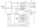
- FIG. 2is a block diagram illustrating a disk drive system 200 according to an embodiment of the present invention.
- the system 200includes a disk controller 210 , a read channel circuit 215 , a write channel circuit 220 , one or more read heads 64 a and one or more write heads 64 b .
- the disk drive system 200may include a read head 64 a and a write read 64 b for each surface of a disk 46 of the disk drive 100 .
- the disk controller 210controls various operations of the disk drive system 200 , as discussed further below.
- the read channel circuit 215reads data from the disk(s) 46 using the read head 64 a and sends the read data to the disk controller 210 .
- the write channel circuit 220receives data from the disk controller 210 and writes the data to the disk(s) 46 using one or more write heads 64 b .
- the disk controller 210 , the read channel circuit 215 and the write channel circuit 220may be mounted on the PCBA 114 shown in FIG. 1 .
- the disk controller 210receives data to be written to the disk(s) 46 from a host computing device.
- the host computing devicemay be a desktop computer, a laptop computer, a mobile computing device, or any type of computing device utilizing a disk drive.
- the disk controller 210may temporarily store the received data in cache memory, which may comprise a random access memory (RAM).
- RAMrandom access memory
- the disk controller 210To write the data to the disk(s) 46 , the disk controller 210 reads the data from the cache memory and sends the data in sectors to the write channel circuit 220 . For each data sector, the disk controller 210 may also send a write address identifying an address on the disk(s) 46 at which the data sector is to be written. The write address may include a track and sector ID identifying a track and sector on the disk(s) 46 . The disk controller 210 also controls the spindle motor 113 to rotate the disk(s) 46 and controls the VCM coil 150 to move the actuator arms 160 to position the write head 64 b over a desired track on the disk(s) 46 .
- the disk controller 210may also generate and add error correcting code (ECC) to each data sector before sending the data sector to the write channel circuit 220 .
- ECCerror correcting code
- the ECCallows the disk controller 210 to later detect and correct errors in the data sector when the data sector is subsequently read from the disk(s) 46 .
- the ECCmay also be used to indicate whether the corresponding data sector is valid. If the data sector is error free or has errors that can be corrected by the ECC, then the data sector may be deemed valid. If the data sector has errors and the ECC fails to correct the errors, then the data sector may be deemed invalid.
- the write channel circuit 220includes a write data buffer 225 and a write address buffer 235 for temporarily storing a data sector and the corresponding write address, respectively, received from the disk controller 210 .
- the write data buffer 225comprises high-speed volatile memory (e.g., static random access memory (SRAM)) to support fast disk write operations.
- SRAMstatic random access memory
- the write channel circuit 220may receive the sector data from the disk controller 210 serially or in parallel.
- the write channel circuit 220may receive the sector data over a parallel bus, in which multiple bits of the data sector are received at a time depending on the width of the parallel bus.
- the parallel busmay have a width of 16 bits or other widths.
- the write channel circuit 220sends the sector data from the write buffer 225 to the write head 64 b when the write head 64 b is positioned over a location of the disk(s) 46 corresponding to the write address.
- the write head 64 bthen magnetically writes the sector data to the disk(s) 46 .
- the write channel circuit 220may send a signal to the disk controller 210 indicating that the data sector has been successfully written to the disk(s) 46 and that the write channel circuit 220 is ready to receive a next data sector to be written to the disk(s) 46 .
- the disk controller 210may send a read address (e.g., track and sector ID) of the data sector to the read channel circuit 215 .
- the disk controller 210also controls the spindle motor 113 to rotate the disk(s) 46 and controls VCM coil 150 to move the actuator arms 160 to position the read head 64 a over the desired track of the disk(s) 46 .
- the read channel circuit 215then reads the data sector from the disk(s) 46 using the read head 64 a when the read head 64 a is positioned over a location of the disk(s) 46 corresponding to the read address.
- the read channel circuit 215then sends the read data sector to the disk controller 210 .
- the disk controller 215may check the ECC of the sector data to detect and correct errors in the read sector data. If the data sector is read in response to a read request from the host computing device, then the disk controller 210 sends the read data sector to the host computing device.
- the disk drive system 200also includes a control circuit 240 , a second write data buffer 250 , a second write address buffer 255 , a write clean/dirty buffer 260 , an ECC buffer 270 , and a backup power device 275 that provides power to the buffers 250 , 255 , 260 and 270 .
- the backup power device 275is configured to continue to provide power to the buffers 250 , 255 , 260 and 270 when there is a power failure of the system 200 , as discussed further below.
- the portion of the system 200 that receives power from the backup power device 275may be referred to as a power island 245 . As shown in FIG. 2 , the buffers 250 , 255 , 260 and 270 are located within the power island 245 .
- the write channel circuit 220 , the read channel circuit 215 , and the disk controller 210receive power from a common power supply.
- the backup power device 275continues to provide power to the buffers 250 , 255 , 260 and 270 within the power island 245 to hold the contents of the buffers 250 , 255 , 260 and 270 .
- the backup power device 275may do this by storing energy from the power supply when the power supply is running and using the stored energy to provide power to the buffers 250 , 255 , 260 and 270 when the power supply fails.
- the backup power device 275may store the energy using one or more capacitors, a battery, or other suitable energy storage devices.
- FIG. 3is a block diagram of an example backup power device 275 according to an embodiment of the invention.
- the backup power device 275comprises one or more capacitors 310 coupled to a power line 320 , a switch 325 and a switch control 330 .
- the power line 320provides power to the buffers 250 , 255 , 260 and 270 .
- the switch 325couples or decouples a power supply voltage Vpwr to the power line 320 and the capacitor(s) 310 depending on whether there is a power failure of the system 200 , as discussed further below.
- the power supply voltage Vpwrmay be from the same power supply that provides power to the write channel circuit 220 , the read channel circuit 210 , and the disk controller 215 .
- the switch 325may be implemented with a Field Effect Transistor (FET) or other switching devices.
- FETField Effect Transistor
- the switch control 330is configured to close the switch 325 when the power supply voltage Vpwr is above a threshold level and to open the switch 325 when the power supply voltage Vpwr falls below the threshold level due to a power failure.
- the switch 325couples the power line 320 to the power supply voltage Vpwr to provide power to the buffers 250 , 255 , 260 and 270 .
- the switch 325also couples the capacitor(s) 310 to the power supply voltage Vpwr to charge up the capacitor(s) 310 . Assuming a small voltage drop across the switch 325 , the capacitor(s) 325 is charged to a voltage approximately equal to the power supply voltage Vpwr.
- the switch 325When the switch 325 is opened in the event of a power failure, the switch 325 decouples the power line 320 and the capacitor(s) 310 from the power supply voltage Vpwr. The charge stored on the capacitor(s) 310 maintains a voltage on the power line 320 sufficient to hold the contents of the buffers 250 , 255 , 260 and 270 for an extended period of time after the power failure. In some embodiments, the extended period of time may be hours, days or weeks.
- the backup power device 275may include a rechargeable battery or other energy storage device coupled to the power line 320 instead of or in addition to the capacitor(s) 310 . Also, the backup power device 275 may include a diode between the power line 320 and the power supply voltage Vpwr instead of the switch 325 . In this embodiment, the diode allows current flow in a direction from the power supply voltage Vpwr to the power line 320 while blocking current in the opposite direction. This prevents the capacitor(s) 310 from discharging when the power supply voltage drops Vpwr below the voltage of the capacitor(s) 310 due to a power failure.
- the control circuit 240is configured to write a duplicate copy of the data sector in the write data buffer 225 of the write channel circuit 220 to the second write data buffer 250 during a write operation.
- the control circuit 240may receive the data sector from the same output of the disk controller 210 as the write channel circuit 220 , as shown in the example in FIG. 2 .
- the second write data buffer 250may comprise volatile memory (e.g., static random access memory (SRAM)) that can be written to and read from at high data rates.
- SRAMstatic random access memory
- control circuit 240may minor the current contents of the write data buffer 225 in the second write data buffer 250 as the write data buffer 220 receives new data sectors and overwrites old data sectors that have already been written to the disk(s) 46 .
- the control circuit 240may write the duplicate data sector to the second write data buffer 250 at a data rate of 10 Megabytes/seconds or higher.
- the control circuit 240may write a data sector to the second write data buffer 250 serially or in parallel.
- the control circuit 240also writes a duplicate copy of the write address in the write address buffer 235 of the write channel circuit 220 into the second write address buffer 255 .
- the write addressmay include a track and sector ID identifying a track and sector on the disk(s) 46 .
- the write addressmay also include a servo wedge number.
- the control circuit 240may receive the write address from the same output of the disk controller 210 as the write channel circuit 220 .
- the control circuit 240also stores a flag in the write clean/dirty buffer 260 indicating whether the current data sector in the write buffer 225 has been completely written to the disk(s) 46 .
- the flagis set to clean when the data sector in the write data buffer 225 has been completely written to the disk(s) 46 and is set to dirty when the data sector has not been completely written to the disk(s) 46 (i.e., the data sector write to the disk(s) 46 is in progress).
- the control circuit 240may determine when the data sector has been completely written to the disk(s) 46 by receiving a signal from the write channel circuit 220 or other circuitry (e.g., servo circuitry) indicating that the data sector has been successfully written to the disk(s) 46 .
- control circuit 240may set the flag in the write clean/dirty buffer 260 to dirty when a data sector is first written to the write data buffer 225 .
- the control circuit 240may then set the flag in the clean/dirty buffer 260 to clean when the control circuit 240 receives a signal from the write channel circuit 220 indicating that the data sector has been successfully written to the disk(s) 46 .
- the control circuit 240may also generate ECC code for the write address and the flag and store the ECC in the ECC buffer 270 . As discussed below, the ECC is used to determine whether the write address and the flag in the second write address buffer 255 and the write clean/dirty buffer 260 , respectively, are valid.
- buffers 250 , 255 , 260 and 270are shown separately in FIG. 2 for ease of illustration, they may be implemented in one physical buffer with different portions of the buffer allocated for the data sector, the write address, the flag and the ECC.
- the backup power device 275continues to provide power to the buffers 250 , 255 , 260 and 270 when there is a power failure of the system 200 to hold the contents of the buffers 250 , 255 , 260 and 270 .
- the backup power device 275may provide power to the buffers 250 , 255 , 260 and 270 for an extended period of time after a power failure. This allows the second write data buffer 225 to hold the duplicate data sector for an extended period of time after the corresponding data sector in the write data buffer 225 is lost due to a power failure during a write operation.
- the disk controller 210uses the duplicate data sector in the second write data buffer 250 to detect and correct a write splice failure that may have occurred due to the power failure, as discussed below.
- FIG. 4is a flowchart illustrating a method for mirroring the current contents of the write data buffer 225 in the second write data buffer 255 in the power island 275 according to an embodiment of the invention. The method may be performed by the write channel circuit 220 and the control circuit 240 .
- step 410the write channel circuit 220 and the control circuit 240 receive a data sector from the disk controller 210 .
- the write channel circuit 220writes the data sector to the write data buffer 225 .
- the control circuit 240writes the data sector to the second write data buffer 250 in the power island 245 . Steps 420 and 430 may be performed in parallel.
- the second write data buffer 250stores a duplicate of the data sector in the write data buffer 225 .
- the control circuit 240may write a duplicate of the write address in the write address buffer 235 into the second write address buffer 255 .
- step 440the control circuit 240 sets the flag in the write clean/dirty buffer 260 to dirty to indicate that the data sector in the write data buffer 225 has not been completely written to the disk(s) 46 (i.e., the data sector write to the disk(s) 46 is in progress).
- step 450the write channel circuit 220 writes the data sector from the write data buffer 225 to the disk(s) 46 using the write head 64 b .
- step 460the write channel circuit 220 determines whether the data sector in the write data buffer 225 is completely written to the disk(s) 46 .
- the write channel circuit 220continues writing the data sector from the write data buffer 225 to the disk(s) 46 in step 450 . If the data sector is completely written to the disk(s) 46 , then the write channel circuit 220 sends a signal to the control circuit 240 indicating that the data sector has been successfully written to the disk(s) 46 .
- step 470the control circuit 240 sets the flag in the write clean/dirty buffer 260 to clean to indicate that the data sector in the write data buffer 225 has been completely written to the disk(s) 46 .
- the methodmay return to step 410 to repeat steps 410 through 470 for a next data sector from the disk controller 210 to written to the disk(s) 46 .
- the control circuit 240may also generate ECC for the write address and the flag in the second write address buffer 255 and the write clean/dirty buffer 260 , respectively, and store the ECC in the ECC buffer 270 . As discussed below, the ECC may be used to determine whether the write address and the flag are valid.
- the backup power device 275When there is a power failure of the system 200 , the backup power device 275 provides power to the buffers 250 , 255 , 260 and 270 to hold the contents of the buffers 250 , 255 , 260 and 270 for an extended period of time.
- the state of the flag in the write clean/dirty buffer 260indicates whether the data sector that was in the write data buffer 225 at the time of the power failure was completely written to the disk(s) 46 before the power failure.
- a dirty flagindicates that the data sector was not completely written to the disk(s) 46 before the power failure while a clean flag indicates that the data sector was completely written to the disk(s) before the power failure. If the data sector was not written to the disk(s) before the power failure resulting in a write splice, then the disk controller 210 may use the duplicate data sector stored in the second write data buffer 250 to correct the write splice, as discussed below.
- FIG. 5is a flowchart illustrating a method for correcting a write splice on the disk(s). The method may be performed the next time the system 200 is powered up after a power failure and may be performed by the disk controller 210 , the write channel circuit 220 and the control circuit 240 .
- the disk controller 210reads the contents of the buffers 250 , 255 , 260 and 270 in the power island 275 .
- the disk controller 210checks the flag from the write clean/dirty buffer 260 to determine whether the data sector that was in the write data buffer 225 at the time of a power failure was completely written to the disk(s) 46 before the power failure.
- the disk controller 210may also check the ECC from the ECC buffer 270 to determine whether the write address and the flag from the second write address buffer 255 and the write clean/dirty buffer 260 , respectively, are valid. If the write address and flag are invalid, then the method ends.
- the disk controller 210determines whether the flag from the write clean/dirty buffer 260 is dirty. If the flag is not dirty (i.e., clean), then the method ends in step 540 . If the flag is dirty, then the disk controller 210 corrects the disk(s) with the data sector from the second write data buffer 250 in step 550 . The disk controller 210 may do this by sending the data sector and the write address from the second write data buffer 250 and the second write address buffer 255 , respectively, to the write channel circuit 220 to write the data sector to the disk(s) 46 at the address on the disk(s) 46 specified by the write address. Thus, when a write splice occurs on the disk(s) 46 due to a power failure during a write operation, the disk controller 210 corrects the write splice using the data sector from the second write data buffer 250 in the power island 245 .
- the disk controller 210may verify whether a write splice is present on the disk(s) 46 at the address specified by the write address from the second write buffer 250 .
- the disk controller 210may read the data sector from the disk(s) 46 at the address specified by the write address using the read channel circuit 215 .
- the disk controller 210may then check the ECC in the data sector read from the disk(s) 46 to determine whether a write splice is present. If the ECC in the data sector from the disk(s) 46 indicates that the data sector is invalid, then the disk controller 210 may determine that a write splice is present on the disk(s) 46 and correct the write splice in step 550 . If the ECC in the data sector from the disk(s) 46 indicates that the data sector is valid, then the disk controller 210 may determine that a write splice is not present on the disk(s) 46 and skip step 550 .
- the disk controller 210may read the data sector from the disk(s) 46 at the address specified by the write address from the second write buffer 250 and compare the data sector from the disk(s) 46 with the data sector from the second write data buffer 250 . If the two data sectors match, then the disk controller 210 may determine that a write splice is not present on the disk(s) 46 and skip step 550 . The disk controller 210 may perform the comparison after the two data sectors have been corrected for errors using the respective ECCs.
- the write clean/dirty flag buffer 260may be omitted.
- the disk controller 210may determine whether a write splice is present on the disk(s) at power up by reading the data sector from the disk(s) 46 at the address specified by the write address from the second write address buffer 255 . The disk controller 210 may then compare the data sector read from the disk(s) 46 with the data sector read from the second write data buffer 250 . If the two data sectors do not match, then the disk controller 210 may determine that a write splice is present and correct the write splice on the disk(s) 46 using the data sector from the second write data buffer 250 in step 550 .
- the disk controller 210may verify whether the data sector from the second write buffer 250 is valid by checking the ECC in the data sector from the second write data buffer 250 . If the ECC indicates that the data sector is valid, then the disk controller 210 may determine that the data sector from the second write buffer 250 is valid and proceed with correcting the disk(s) 46 using the data sector from the second write buffer 250 . However, if the ECC in the data sector from second write buffer 250 indicates the data sector is invalid, then the disk controller 210 may skip writing the data sector from the second write buffer 250 to the disk(s) 46 since the data sector is invalid.
- the contents of the buffers 250 , 255 and 260may become invalid when the system 200 remains off for a long period of time and the backup power device 275 is unable to provide power for the long period of time.
- the capacitor(s) 310 in the backup power device 275may slowly leak charge over time causing the voltage on the power line 320 to eventually fall below a voltage sufficient to hold the contents of the buffers 250 , 255 , 260 and 270 when the system 200 remains off for too long.
- the disk controller 210may determine whether the voltage on the power line 320 is sufficient to hold the contents of the buffers 250 , 255 , 260 and 270 by checking the voltage on the power line 320 with a voltage detector just prior to the switch 325 being closed at power up.
- FIG. 6is a block diagram illustrating the backup power device 275 including a voltage detector 610 coupled to the power line 320 according to an embodiment of the invention.
- the control circuit 240checks the voltage on the power line 320 using the voltage detector 610 just prior to the switch 325 being closed at power up. If the detected voltage is above a predetermined threshold voltage, then the control circuit 240 may send a signal to the disk controller 210 to proceed with reading the contents from the buffers 250 , 255 , 260 and 270 .
- the threshold voltagemay be based on a minimum voltage needed to hold the contents of the buffers 250 , 255 , 260 and 270 .
- the disk controller 210may also determine whether the contents of the buffers 250 , 255 and 260 are valid by checking the ECC in the data sector from the second write data buffer 250 and/or checking the ECC of the write address and the flag from the second write buffer 255 and the write clean/dirty buffer 260 , respectively.
- the disk drive system 200is capable of detecting and correcting a write splice on the disk(s) 46 caused by a power failure.
- the disk drive system 200provide one or more of the following advantages.
- One advantageis that the disk drive system 200 prevents a write splice from causing a read failure by correcting the write splice when the system 200 is powered up after a power failure. This reduces the likelihood that disk drive will be declared bad because of read failures due to write splices.
- Another advantageis that the buffers 250 , 255 , 260 and 270 store a relatively small amount of data, and can therefore be made small and inexpensively.
- Another advantageis that the buffers 250 , 255 , 260 and 270 and the control circuit 240 can be integrated with other components of the system 200 on a chip to further reduce cost.
- the switch 325 , power line 320 and switch control 330 of the backup power deice 275may also be integrated with other components of the system 200 on a chip.
- the capacitor(s) 310 of the backup power device 275may be implemented with an external capacitor that is coupled to the switch 325 on the chip through a pin or other electrical contact on the chip.
- the backup power device 275may also be used to provide power to other components of the disk drive system 200 .
- FIG. 7shows a drive system 700 according an embodiment in which the second write data buffer 250 and the second write address buffer 255 are omitted.
- the backup power device 275is coupled to the write data buffer 225 and the write address buffer 235 of the write channel circuit 220 to hold the contents of the buffers 225 and 235 in the event of a power failure.
- read data pathsare provided from the buffers 225 and 235 to the disk controller 210 for the disk controller 210 to read the contents of the buffers 225 and 235 .
- the backup power device 275continues to provide power to the write data buffer 225 and the write address buffer 235 to hold the data sector and write address, respectively.
- the disk controller 210reads the data sector and the write address from the write data buffer 225 and the write address buffer 235 , respectively.
- the disk controller 210may then use the read sector data and write address to correct a write splice on the disk(s) 46 that may have occurred due to the power failure using any one of the methods discussed above.
- Embodiments of the inventionmay also be used to correct write splices for other storage media.
- embodiments of the inventionmay be used to correct write splices in a solid state memory (e.g., flash memory).
- FIG. 8shows an embodiment of a system 800 for correcting write splices in a solid state memory 820 .
- a controller 810sends data to be written to the solid state memory 820 to a write data buffer 225 . The data may then be written from the write data buffer 225 to the solid state memory 820 .
- the controller 810may correct a write splice in the solid state memory 820 that may have occurred due to the power failure using any of the methods discussed above.
- the controller 810 , the read channel circuit 215 and/or the write channel circuit 220may be separate from the solid state memory 820 or integrated with the solid state memory 820 on a single chip.
- the disk controller 210 and the control circuit 240may be implemented with a general purpose processor, a digital signal processor (DSP), an application specific integrated circuit (ASIC), a field programmable gate array (FPGA) or other programmable logic device, discrete gate or transistor logic, discrete hardware components, or any combination thereof designed to perform the functions described herein.
- the disk controller 210 and the control circuit 240may also include software code that is stored in a machine-readable medium and executed by a processor to perform the functions described herein.
Landscapes
- Techniques For Improving Reliability Of Storages (AREA)
Abstract
Description
Claims (30)
Priority Applications (1)
| Application Number | Priority Date | Filing Date | Title |
|---|---|---|---|
| US12/533,993US8370683B1 (en) | 2009-07-31 | 2009-07-31 | System and method to reduce write splice failures |
Applications Claiming Priority (1)
| Application Number | Priority Date | Filing Date | Title |
|---|---|---|---|
| US12/533,993US8370683B1 (en) | 2009-07-31 | 2009-07-31 | System and method to reduce write splice failures |
Publications (1)
| Publication Number | Publication Date |
|---|---|
| US8370683B1true US8370683B1 (en) | 2013-02-05 |
Family
ID=47604726
Family Applications (1)
| Application Number | Title | Priority Date | Filing Date |
|---|---|---|---|
| US12/533,993Expired - Fee RelatedUS8370683B1 (en) | 2009-07-31 | 2009-07-31 | System and method to reduce write splice failures |
Country Status (1)
| Country | Link |
|---|---|
| US (1) | US8370683B1 (en) |
Cited By (126)
| Publication number | Priority date | Publication date | Assignee | Title |
|---|---|---|---|---|
| US8879188B1 (en) | 2010-08-23 | 2014-11-04 | Western Digital Technologies, Inc. | Disk drive employing fly height calibration tracks to account for magnetic entropy and thermal decay |
| US8891193B1 (en) | 2013-05-09 | 2014-11-18 | Western Digital Technologies, Inc. | Disk drive calibrating threshold and gain of touchdown sensor |
| US8891341B1 (en) | 2013-03-11 | 2014-11-18 | Western Digital Technologies, Inc. | Energy assisted magnetic recording disk drive using modulated laser light |
| US8902529B1 (en) | 2012-11-20 | 2014-12-02 | Western Digital Technologies, Inc. | Dual frequency crystal oscillator |
| US8902527B1 (en) | 2010-03-22 | 2014-12-02 | Western Digital Technologies, Inc. | Systems and methods for improving sequential data rate performance using sorted data zones |
| US8908311B1 (en) | 2014-01-27 | 2014-12-09 | Western Digital Technologies, Inc. | Data storage device writing a multi-sector codeword in segments over multiple disk revolutions |
| US8909889B1 (en) | 2011-10-10 | 2014-12-09 | Western Digital Technologies, Inc. | Method and apparatus for servicing host commands by a disk drive |
| US8914625B1 (en) | 2009-07-31 | 2014-12-16 | Western Digital Technologies, Inc. | Automatically configuring a web browser file when booting an operating system from a data storage device |
| US8922939B1 (en) | 2013-04-02 | 2014-12-30 | Western Digital Technologies, Inc. | Disk drive generating feed-forward fly height control based on temperature sensitive fly height sensor |
| US8937782B1 (en) | 2012-05-07 | 2015-01-20 | Western Digital Technologies, Inc. | Hard disk drive assembly including a NVSM to store configuration data for controlling disk drive operations |
| US8941941B1 (en) | 2013-02-28 | 2015-01-27 | Western Digital Technologies, Inc. | Disk drive calibrating touchdown sensor |
| US8947812B1 (en) | 2014-03-27 | 2015-02-03 | Western Digital Technologies, Inc. | Data storage device comprising equalizer filter and inter-track interference filter |
| US8949521B1 (en) | 2013-04-10 | 2015-02-03 | Western Digital Technologies, Inc. | Actuator prepositioning for disk drive |
| US8954664B1 (en) | 2010-10-01 | 2015-02-10 | Western Digital Technologies, Inc. | Writing metadata files on a disk |
| US8953277B1 (en) | 2014-06-16 | 2015-02-10 | Western Digital Technologies, Inc. | Data storage device writing tracks on a disk with equal spacing |
| US8953269B1 (en) | 2014-07-18 | 2015-02-10 | Western Digital Technologies, Inc. | Management of data objects in a data object zone |
| US8958167B1 (en) | 2013-12-23 | 2015-02-17 | Western Digital Technologies, Inc. | Detection of disk surface irregularities in data storage devices |
| US8959281B1 (en) | 2012-11-09 | 2015-02-17 | Western Digital Technologies, Inc. | Data management for a storage device |
| US8970978B1 (en) | 2012-10-22 | 2015-03-03 | Western Digital Technologies, Inc. | Disk drive detecting head touchdown by applying DC+AC control signal to fly height actuator |
| US8976633B1 (en) | 2014-04-15 | 2015-03-10 | Western Digital Technologies, Inc. | Data storage device calibrating fly height actuator based on laser power for heat assisted magnetic recording |
| US8990493B1 (en) | 2011-06-30 | 2015-03-24 | Western Digital Technologies, Inc. | Method and apparatus for performing force unit access writes on a disk |
| US8988810B1 (en) | 2014-04-16 | 2015-03-24 | Western Digital Technologies, Inc. | Track measurement for data storage device |
| US8988809B1 (en) | 2014-02-18 | 2015-03-24 | Western Digital (Fremont), Llc | Disk recording device for writing a radially coherent reference band by measuring relative timing offsets of reference bursts |
| US8996839B1 (en) | 2012-01-23 | 2015-03-31 | Western Digital Technologies, Inc. | Data storage device aligning partition to boundary of sector when partition offset correlates with offset of write commands |
| US9001453B1 (en) | 2014-07-18 | 2015-04-07 | Western Digital Technologies, Inc. | Data storage device calibrating fly height actuator based on read mode touchdown resistance of touchdown sensor |
| US9009358B1 (en) | 2008-09-23 | 2015-04-14 | Western Digital Technologies, Inc. | Configuring a data storage device with a parameter file interlocked with configuration code |
| US9013818B1 (en) | 2013-12-06 | 2015-04-21 | Western Digital Technologies, Inc. | Disk drive measuring reader/writer gap by measuring fractional clock cycle over disk radius |
| US9013821B1 (en) | 2014-06-10 | 2015-04-21 | Western Digital Technologies, Inc. | Data storage device employing one-dimensional and two-dimensional channels |
| US9021410B1 (en) | 2013-12-10 | 2015-04-28 | Western Technologies, Inc. | Electronic system with multi-cycle simulation coverage mechanism and method of operation thereof |
| US9025421B1 (en) | 2014-10-08 | 2015-05-05 | Western Digital Technologies, Inc. | Data storage device adjusting laser input power to compensate for temperature variations |
| US9025267B1 (en) | 2014-06-09 | 2015-05-05 | Western Digital Technologies, Inc. | Data storage device using branch metric from adjacent track to compensate for inter-track interference |
| US9025270B1 (en) | 2013-09-17 | 2015-05-05 | Western Digital Technologies, Inc. | Electronic system with current conservation mechanism and method of operation thereof |
| US9049471B2 (en) | 2001-10-17 | 2015-06-02 | Keen Personal Media, Inc. | Personal video recorder for inserting a stored advertisement into a displayed broadcast stream |
| US9047917B1 (en) | 2013-11-26 | 2015-06-02 | Western Digital Technologies, Inc. | Disk drive slider with sense amplifier for coupling to a preamp through a supply/bias line and a read signal line |
| US9053730B1 (en) | 2012-05-11 | 2015-06-09 | Western Digital Technologies, Inc. | Disk drive comprising extended range head proximity sensor |
| US9053749B1 (en) | 2013-03-15 | 2015-06-09 | Western Digital Technologies, Inc. | Disk drive comprising a per-drive and per-head fly height filter |
| US9060420B2 (en) | 2007-11-01 | 2015-06-16 | Western Digitial Technologies, Inc. | Method of manufacturing a double sided flex circuit for a disk drive wherein a first side lead provides an etching mask for a second side lead |
| US9064542B1 (en) | 2013-04-08 | 2015-06-23 | Western Digital Technologies, Inc. | Scheduled load of heads to reduce lubricant migration on pole tip and decrease time to ready |
| US9063838B1 (en) | 2012-01-23 | 2015-06-23 | Western Digital Technologies, Inc. | Data storage device shifting data chunks of alignment zone relative to sector boundaries |
| US9064504B1 (en) | 2014-01-29 | 2015-06-23 | Western Digital Technologies, Inc. | Electronic system with media recovery mechanism and method of operation thereof |
| US9064525B2 (en) | 2013-11-26 | 2015-06-23 | Western Digital Technologies, Inc. | Disk drive comprising laser transmission line optimized for heat assisted magnetic recording |
| US9070406B1 (en) | 2014-03-10 | 2015-06-30 | Western Digital Technologies, Inc. | Disk drive configuring one-dimensional and two-dimensional recording areas based on read element spacing |
| US9075714B1 (en) | 2014-05-13 | 2015-07-07 | Western Digital Technologies, Inc. | Electronic system with data management mechanism and method of operation thereof |
| US9074941B1 (en) | 2013-03-14 | 2015-07-07 | Western Digital Technologies, Inc. | Systems and methods for measuring ambient and laser temperature in heat assisted magnetic recording |
| US9076474B1 (en) | 2014-12-23 | 2015-07-07 | Western Digital Technologies, Inc. | Data storage device attenuating thermal decay effect on fly height measurement |
| US9082458B1 (en) | 2014-03-10 | 2015-07-14 | Western Digital Technologies, Inc. | Data storage device balancing and maximizing quality metric when configuring arial density of each disk surface |
| US9099144B1 (en) | 2013-10-11 | 2015-08-04 | Western Digital Technologies, Inc. | Disk drive evaluating laser performance for heat assisted magnetic recording |
| US9099134B1 (en) | 2015-01-27 | 2015-08-04 | Western Digital Technologies, Inc. | Data storage device employing multiple jog profiles for a butterfly written disk surface |
| US9099103B1 (en) | 2014-10-21 | 2015-08-04 | Western Digital Technologies, Inc. | Heat assisted magnetic recording withinterlaced high-power heated and low-power heated tracks |
| US9117489B1 (en) | 2014-02-18 | 2015-08-25 | Western Digital Technologies, Inc. | Data storage device screening heads by verifying defects after defect scan |
| US9117479B1 (en) | 2014-09-24 | 2015-08-25 | Western Digital Technologies, Inc. | Data storage device calibrating laser write power for heat assisted magnetic recording |
| US9117463B1 (en) | 2014-06-23 | 2015-08-25 | Western Digital Technologies, Inc. | Data storage device erasing multiple adjacent data tracks to recover from inter-track interference |
| US9123370B1 (en) | 2014-04-15 | 2015-09-01 | Western Digital Technologies, Inc. | Data storage device calibrating fly height actuator based on laser power for heat assisted magnetic recording |
| US9123382B1 (en) | 2014-10-28 | 2015-09-01 | Western Digital Technologies, Inc. | Non-volatile caching for sequence of data |
| US9129628B1 (en) | 2014-10-23 | 2015-09-08 | Western Digital Technologies, Inc. | Data management for data storage device with different track density regions |
| US9128820B1 (en) | 2012-06-18 | 2015-09-08 | Western Digital Technologies, Inc. | File management among different zones of storage media |
| US9135205B1 (en) | 2013-05-01 | 2015-09-15 | Western Digital Technologies, Inc. | Data storage assembly for archive cold storage |
| US9153287B1 (en) | 2013-05-13 | 2015-10-06 | Western Digital Technologies, Inc. | Data access for shingled magnetic recording media |
| US9153266B1 (en) | 2014-09-11 | 2015-10-06 | Western Digital Technologies, Inc. | Data storage device measuring laser protrusion fly height profile |
| US9158722B1 (en) | 2011-11-02 | 2015-10-13 | Western Digital Technologies, Inc. | Data storage device to communicate with a host in a SATA or a USB mode |
| US9164694B1 (en) | 2013-06-19 | 2015-10-20 | Western Digital Technologies, Inc. | Data storage device detecting read-before-write conditions and returning configurable return data |
| US9171575B1 (en) | 2014-06-23 | 2015-10-27 | Western Digital Technologies, Inc. | Data storage device detecting media defects by writing opposite polarity test pattern |
| US9183864B1 (en) | 2013-06-13 | 2015-11-10 | Western Digital Technologies, Inc. | Disk drive adjusting closed-loop fly height target based on change in open-loop fly height control signal |
| US9183877B1 (en) | 2015-03-20 | 2015-11-10 | Western Digital Technologies, Inc. | Data storage device comprising two-dimensional data dependent noise whitening filters for two-dimensional recording |
| US9189392B1 (en) | 2011-06-30 | 2015-11-17 | Western Digital Technologies, Inc. | Opportunistic defragmentation during garbage collection |
| US9196302B1 (en) | 2015-03-18 | 2015-11-24 | Western Digital Technologies, Inc. | Electronic system with media maintenance mechanism and method of operation thereof |
| US9213493B1 (en) | 2011-12-16 | 2015-12-15 | Western Digital Technologies, Inc. | Sorted serpentine mapping for storage drives |
| US9214186B1 (en) | 2015-03-23 | 2015-12-15 | Western Digital Technologies, Inc. | Data storage device measuring radial offset between read element and write element |
| US9230605B1 (en) | 2014-12-01 | 2016-01-05 | Western Digital Technologies, Inc. | Data storage device maximizing areal density based on a target quality metric |
| US9230585B1 (en) | 2014-01-31 | 2016-01-05 | Western Digital Technologies, Inc. | Per wedge preheat DFH to improve data storage device performance |
| US9236086B1 (en) | 2014-10-15 | 2016-01-12 | Western Digital Technologies, Inc. | Methods for reducing operational latency of data storage systems |
| US9245556B2 (en) | 2014-03-10 | 2016-01-26 | Western Digital Technologies, Inc. | Disk drive employing multiple read elements to increase radial band for two-dimensional magnetic recording |
| US9245558B1 (en) | 2014-05-09 | 2016-01-26 | Western Digital Technologies, Inc. | Electronic system with data management mechanism and method of operation thereof |
| US9251856B1 (en) | 2014-05-30 | 2016-02-02 | Western Digial Technologies, Inc. | Read failover method and apparatus for a data storage system |
| US9251844B1 (en) | 2014-06-02 | 2016-02-02 | Western Digital Technologies, Inc. | Waterfall method and apparatus for a data storage device read system |
| US9257143B1 (en) | 2014-12-23 | 2016-02-09 | Western Digital Technologies, Inc. | Precautionary measures for data storage device environmental conditions |
| US9257146B1 (en) | 2014-02-11 | 2016-02-09 | Western Digital Technologies, Inc. | Data storage device comprising sequence detector compensating for inter-track interference |
| US9257145B1 (en) | 2013-11-27 | 2016-02-09 | Western Digital Technologies, Inc. | Disk drive measuring down-track spacing of read sensors |
| US9263088B2 (en) | 2014-03-21 | 2016-02-16 | Western Digital Technologies, Inc. | Data management for a data storage device using a last resort zone |
| US9269393B1 (en) | 2014-12-08 | 2016-02-23 | Western Digital Technologies, Inc. | Electronic system with data refresh mechanism and method of operation thereof |
| US9268649B1 (en) | 2011-06-23 | 2016-02-23 | Western Digital Technologies, Inc. | Disk drive with recent write streams list for data refresh determination |
| US9268499B1 (en) | 2010-08-13 | 2016-02-23 | Western Digital Technologies, Inc. | Hybrid drive migrating high workload data from disk to non-volatile semiconductor memory |
| US9281009B1 (en) | 2014-12-18 | 2016-03-08 | Western Digital Technologies, Inc. | Data storage device employing variable size interleave written track segments |
| US9311939B1 (en) | 2014-12-23 | 2016-04-12 | Western Digital Technologies, Inc. | Write-through media caching |
| US9318137B1 (en) | 2015-03-13 | 2016-04-19 | Western Digital Technologies, Inc. | Data storage device executing retry operation by buffering signal samples at different radial offsets |
| US9330715B1 (en) | 2010-03-22 | 2016-05-03 | Western Digital Technologies, Inc. | Mapping of shingled magnetic recording media |
| US9355666B1 (en) | 2013-09-30 | 2016-05-31 | Western Digital Technologies, Inc. | Disk drive measuring stroke difference between heads by detecting a difference between ramp contact |
| US9361938B1 (en) | 2015-04-16 | 2016-06-07 | Western Digital Technologies, Inc. | Disk defect management for a data storage device |
| US9368131B1 (en) | 2015-04-03 | 2016-06-14 | Western Digital (Fremont), Llc | Data storage device employing mirrored cross-track profiles for top and bottom disk surfaces |
| US9368132B1 (en) | 2015-09-04 | 2016-06-14 | Western Digital Technologies, Inc. | Data storage device employing differential write data signal and differential write pattern signal |
| US9383923B1 (en) | 2012-10-18 | 2016-07-05 | Western Digital Technologies, Inc. | Write pointer management for a disk drive |
| US9401165B1 (en) | 2014-05-05 | 2016-07-26 | Western Digital Technologies, Inc. | Method and system to monitor magnetic head loading and unloading stability for a data storage system |
| US9417628B2 (en) | 2013-03-13 | 2016-08-16 | Western Digital Technologies, Inc. | Production failure analysis system |
| US9424864B2 (en) | 2014-07-02 | 2016-08-23 | Western Digital Technologies, Inc. | Data management for a data storage device with zone relocation |
| US9437242B1 (en) | 2015-09-14 | 2016-09-06 | Western Digital Technologies, Inc. | Data storage device employing different frequency preambles in adjacent data tracks |
| US9466318B2 (en) | 2014-12-24 | 2016-10-11 | Western Digital Technologies, Inc. | Allowing fast data zone switches on data storage devices |
| US9466321B1 (en) | 2015-06-05 | 2016-10-11 | Western Digital Technologies, Inc. | Angular position tracking of data accesses to mitigate risk of data loss |
| US9472219B1 (en) | 2015-05-01 | 2016-10-18 | Western Digital Technologies, Inc. | Data storage device calibrating parameter for heat assisted magnetic recording |
| US9502068B1 (en) | 2015-04-08 | 2016-11-22 | Western Digital Technologies, Inc. | Data storage device updating laser power during non-write mode for heat assisted magnetic recording |
| US9501393B2 (en) | 2014-01-27 | 2016-11-22 | Western Digital Technologies, Inc. | Data storage system garbage collection based on at least one attribute |
| US9588898B1 (en) | 2015-06-02 | 2017-03-07 | Western Digital Technologies, Inc. | Fullness control for media-based cache operating in a steady state |
| US9600205B1 (en) | 2014-09-22 | 2017-03-21 | Western Digital Technologies, Inc. | Power aware power safe write buffer |
| US9632711B1 (en) | 2014-04-07 | 2017-04-25 | Western Digital Technologies, Inc. | Processing flush requests by utilizing storage system write notifications |
| US9639287B1 (en)* | 2015-06-29 | 2017-05-02 | Western Digital Technologies, Inc. | Write command reporting |
| US9645752B1 (en) | 2014-04-07 | 2017-05-09 | Western Digital Technologies, Inc. | Identification of data committed to non-volatile memory by use of notification commands |
| US9672107B1 (en) | 2015-02-11 | 2017-06-06 | Western Digital Technologies, Inc. | Data protection for a data storage device |
| US9747928B1 (en) | 2014-09-25 | 2017-08-29 | Western Digital Technologies, Inc. | Data storage device modifying write operation when a laser mode hop is detected |
| US9761273B1 (en) | 2015-11-03 | 2017-09-12 | Western Digital Technologies, Inc. | Data storage device encoding and interleaving codewords to improve trellis sequence detection |
| US9842617B1 (en) | 2015-06-29 | 2017-12-12 | Western Digital Technologies, Inc. | Electronic system with head management mechanism and method of operation thereof |
| US9842622B1 (en) | 2014-12-23 | 2017-12-12 | Western Digital Technologies, Inc. | Data storage device having improved read failure tolerance |
| US9864529B1 (en) | 2014-01-27 | 2018-01-09 | Western Digital Technologies, Inc. | Host compatibility for host managed storage media |
| US9870281B1 (en) | 2015-03-20 | 2018-01-16 | Western Digital Technologies, Inc. | Power loss mitigation for data storage device |
| US9875055B1 (en) | 2014-08-04 | 2018-01-23 | Western Digital Technologies, Inc. | Check-pointing of metadata |
| US9916616B2 (en) | 2014-03-31 | 2018-03-13 | Western Digital Technologies, Inc. | Inventory management system using incremental capacity formats |
| US9933955B1 (en) | 2015-03-05 | 2018-04-03 | Western Digital Technologies, Inc. | Power safe write buffer for data storage device |
| US9952950B1 (en) | 2014-09-08 | 2018-04-24 | Western Digital Technologies, Inc. | Data management in RAID environment |
| US9959052B1 (en) | 2015-09-17 | 2018-05-01 | Western Digital Technologies, Inc. | Media based cache for data storage device |
| US10056920B1 (en) | 2015-11-03 | 2018-08-21 | Western Digital Technologies, Inc. | Data storage device encoding and interleaving codewords to improve trellis sequence detection |
| US10063257B1 (en) | 2015-11-03 | 2018-08-28 | Western Digital Technologies, Inc. | Data storage device encoding and interleaving codewords to improve trellis sequence detection |
| US10168923B2 (en) | 2016-04-26 | 2019-01-01 | International Business Machines Corporation | Coherency management for volatile and non-volatile memory in a through-silicon via (TSV) module |
| US10282371B1 (en) | 2014-12-02 | 2019-05-07 | Western Digital Technologies, Inc. | Object storage device with probabilistic data structure |
| US10282096B1 (en) | 2014-12-17 | 2019-05-07 | Western Digital Technologies, Inc. | Identification of data with predetermined data pattern |
| US10365836B1 (en) | 2015-01-27 | 2019-07-30 | Western Digital Technologies, Inc. | Electronic system with declustered data protection by parity based on reliability and method of operation thereof |
| US10643668B1 (en)* | 2013-08-27 | 2020-05-05 | Seagate Technology Llc | Power loss data block marking |
| US11294592B2 (en) | 2018-01-09 | 2022-04-05 | Alibaba Group Holding Limited | Method and device for data processing, and computer device |
| US20240330113A1 (en)* | 2018-04-06 | 2024-10-03 | Micron Technology, Inc. | Meta Data Protection against Unexpected Power Loss in a Memory System |
Citations (24)
| Publication number | Priority date | Publication date | Assignee | Title |
|---|---|---|---|---|
| US5047988A (en) | 1988-06-17 | 1991-09-10 | Mitsubishi Denki Kabushiki Kaisha | Disposable IC memory card having an embedded battery |
| US5414861A (en) | 1991-09-11 | 1995-05-09 | Fujitsu Limited | Data protection system using different levels of reserve power to maintain data in volatile memories for any period of time |
| US5438549A (en) | 1994-02-28 | 1995-08-01 | Intel Corporation | Nonvolatile memory with volatile memory buffer and a backup power supply system |
| US5448719A (en)* | 1992-06-05 | 1995-09-05 | Compaq Computer Corp. | Method and apparatus for maintaining and retrieving live data in a posted write cache in case of power failure |
| US5586291A (en) | 1994-12-23 | 1996-12-17 | Emc Corporation | Disk controller with volatile and non-volatile cache memories |
| US5596532A (en) | 1995-10-18 | 1997-01-21 | Sandisk Corporation | Flash EEPROM self-adaptive voltage generation circuit operative within a continuous voltage source range |
| US5693570A (en) | 1994-10-17 | 1997-12-02 | Sandisk Corporation | Process for manufacturing a programmable power generation circuit for flash EEPROM memory systems |
| US5706239A (en) | 1996-02-27 | 1998-01-06 | Centennial Technologies, Inc. | Rechargeable SRAM/flash PCMCIA card |
| US5724501A (en)* | 1996-03-29 | 1998-03-03 | Emc Corporation | Quick recovery of write cache in a fault tolerant I/O system |
| US5798961A (en) | 1994-08-23 | 1998-08-25 | Emc Corporation | Non-volatile memory module |
| US6189107B1 (en) | 1997-12-29 | 2001-02-13 | Samsung Electronics Co., Ltd. | Fault tolerant voltage regulator module circuit for supplying core voltage and cache voltage to a processor |
| US6295577B1 (en) | 1998-02-24 | 2001-09-25 | Seagate Technology Llc | Disc storage system having a non-volatile cache to store write data in the event of a power failure |
| US6516426B1 (en) | 1999-01-11 | 2003-02-04 | Seagate Technology Llc | Disc storage system having non-volatile write cache |
| US6760672B2 (en) | 2002-01-29 | 2004-07-06 | Rockwell Automation Technologies, Inc. | Automatic detection of battery-backed data integrity in volatile memory |
| US6798599B2 (en) | 2001-01-29 | 2004-09-28 | Seagate Technology Llc | Disc storage system employing non-volatile magnetoresistive random access memory |
| US6856556B1 (en) | 2003-04-03 | 2005-02-15 | Siliconsystems, Inc. | Storage subsystem with embedded circuit for protecting against anomalies in power signal from host |
| US7003620B2 (en)* | 2002-11-26 | 2006-02-21 | M-Systems Flash Disk Pioneers Ltd. | Appliance, including a flash memory, that is robust under power failure |
| US20060107077A1 (en) | 2004-11-15 | 2006-05-18 | Roth Charles P | Programmable power transition counter |
| US7051306B2 (en) | 2003-05-07 | 2006-05-23 | Mosaid Technologies Corporation | Managing power on integrated circuits using power islands |
| US7100080B2 (en)* | 2002-05-08 | 2006-08-29 | Xiotech Corporation | Write cache recovery after loss of power |
| US20070094446A1 (en)* | 2005-10-20 | 2007-04-26 | Hitachi, Ltd. | Storage system |
| US7363542B2 (en)* | 2002-04-16 | 2008-04-22 | Ricoh Company, Ltd. | Image formation apparatus and network system |
| US7392429B2 (en)* | 2004-12-22 | 2008-06-24 | Microsoft Corporation | System and method for maintaining persistent state data |
| US20100202238A1 (en)* | 2009-02-11 | 2010-08-12 | Stec, Inc. | Flash backed dram module including logic for isolating the dram |
- 2009
- 2009-07-31USUS12/533,993patent/US8370683B1/ennot_activeExpired - Fee Related
Patent Citations (26)
| Publication number | Priority date | Publication date | Assignee | Title |
|---|---|---|---|---|
| US5047988A (en) | 1988-06-17 | 1991-09-10 | Mitsubishi Denki Kabushiki Kaisha | Disposable IC memory card having an embedded battery |
| US5414861A (en) | 1991-09-11 | 1995-05-09 | Fujitsu Limited | Data protection system using different levels of reserve power to maintain data in volatile memories for any period of time |
| US5448719A (en)* | 1992-06-05 | 1995-09-05 | Compaq Computer Corp. | Method and apparatus for maintaining and retrieving live data in a posted write cache in case of power failure |
| US5438549A (en) | 1994-02-28 | 1995-08-01 | Intel Corporation | Nonvolatile memory with volatile memory buffer and a backup power supply system |
| US5798961A (en) | 1994-08-23 | 1998-08-25 | Emc Corporation | Non-volatile memory module |
| US5693570A (en) | 1994-10-17 | 1997-12-02 | Sandisk Corporation | Process for manufacturing a programmable power generation circuit for flash EEPROM memory systems |
| US5586291A (en) | 1994-12-23 | 1996-12-17 | Emc Corporation | Disk controller with volatile and non-volatile cache memories |
| US5596532A (en) | 1995-10-18 | 1997-01-21 | Sandisk Corporation | Flash EEPROM self-adaptive voltage generation circuit operative within a continuous voltage source range |
| US5706239A (en) | 1996-02-27 | 1998-01-06 | Centennial Technologies, Inc. | Rechargeable SRAM/flash PCMCIA card |
| US5724501A (en)* | 1996-03-29 | 1998-03-03 | Emc Corporation | Quick recovery of write cache in a fault tolerant I/O system |
| US6189107B1 (en) | 1997-12-29 | 2001-02-13 | Samsung Electronics Co., Ltd. | Fault tolerant voltage regulator module circuit for supplying core voltage and cache voltage to a processor |
| US6295577B1 (en) | 1998-02-24 | 2001-09-25 | Seagate Technology Llc | Disc storage system having a non-volatile cache to store write data in the event of a power failure |
| US6516426B1 (en) | 1999-01-11 | 2003-02-04 | Seagate Technology Llc | Disc storage system having non-volatile write cache |
| US6798599B2 (en) | 2001-01-29 | 2004-09-28 | Seagate Technology Llc | Disc storage system employing non-volatile magnetoresistive random access memory |
| US6760672B2 (en) | 2002-01-29 | 2004-07-06 | Rockwell Automation Technologies, Inc. | Automatic detection of battery-backed data integrity in volatile memory |
| US7363542B2 (en)* | 2002-04-16 | 2008-04-22 | Ricoh Company, Ltd. | Image formation apparatus and network system |
| US7100080B2 (en)* | 2002-05-08 | 2006-08-29 | Xiotech Corporation | Write cache recovery after loss of power |
| US7003620B2 (en)* | 2002-11-26 | 2006-02-21 | M-Systems Flash Disk Pioneers Ltd. | Appliance, including a flash memory, that is robust under power failure |
| US7126857B2 (en) | 2003-04-03 | 2006-10-24 | Siliconsystems, Inc. | Storage subsystem with embedded circuit for protecting against anomalies in power signal from host |
| US6856556B1 (en) | 2003-04-03 | 2005-02-15 | Siliconsystems, Inc. | Storage subsystem with embedded circuit for protecting against anomalies in power signal from host |
| US7051306B2 (en) | 2003-05-07 | 2006-05-23 | Mosaid Technologies Corporation | Managing power on integrated circuits using power islands |
| US7415680B2 (en) | 2003-05-07 | 2008-08-19 | Mosaid Technologies Corporation | Power managers for an integrated circuit |
| US20060107077A1 (en) | 2004-11-15 | 2006-05-18 | Roth Charles P | Programmable power transition counter |
| US7392429B2 (en)* | 2004-12-22 | 2008-06-24 | Microsoft Corporation | System and method for maintaining persistent state data |
| US20070094446A1 (en)* | 2005-10-20 | 2007-04-26 | Hitachi, Ltd. | Storage system |
| US20100202238A1 (en)* | 2009-02-11 | 2010-08-12 | Stec, Inc. | Flash backed dram module including logic for isolating the dram |
Cited By (135)
| Publication number | Priority date | Publication date | Assignee | Title |
|---|---|---|---|---|
| US9049471B2 (en) | 2001-10-17 | 2015-06-02 | Keen Personal Media, Inc. | Personal video recorder for inserting a stored advertisement into a displayed broadcast stream |
| US9060420B2 (en) | 2007-11-01 | 2015-06-16 | Western Digitial Technologies, Inc. | Method of manufacturing a double sided flex circuit for a disk drive wherein a first side lead provides an etching mask for a second side lead |
| US9009358B1 (en) | 2008-09-23 | 2015-04-14 | Western Digital Technologies, Inc. | Configuring a data storage device with a parameter file interlocked with configuration code |
| US8914625B1 (en) | 2009-07-31 | 2014-12-16 | Western Digital Technologies, Inc. | Automatically configuring a web browser file when booting an operating system from a data storage device |
| US8902527B1 (en) | 2010-03-22 | 2014-12-02 | Western Digital Technologies, Inc. | Systems and methods for improving sequential data rate performance using sorted data zones |
| US9330715B1 (en) | 2010-03-22 | 2016-05-03 | Western Digital Technologies, Inc. | Mapping of shingled magnetic recording media |
| US9268499B1 (en) | 2010-08-13 | 2016-02-23 | Western Digital Technologies, Inc. | Hybrid drive migrating high workload data from disk to non-volatile semiconductor memory |
| US8879188B1 (en) | 2010-08-23 | 2014-11-04 | Western Digital Technologies, Inc. | Disk drive employing fly height calibration tracks to account for magnetic entropy and thermal decay |
| US8954664B1 (en) | 2010-10-01 | 2015-02-10 | Western Digital Technologies, Inc. | Writing metadata files on a disk |
| US9268649B1 (en) | 2011-06-23 | 2016-02-23 | Western Digital Technologies, Inc. | Disk drive with recent write streams list for data refresh determination |
| US9189392B1 (en) | 2011-06-30 | 2015-11-17 | Western Digital Technologies, Inc. | Opportunistic defragmentation during garbage collection |
| US8990493B1 (en) | 2011-06-30 | 2015-03-24 | Western Digital Technologies, Inc. | Method and apparatus for performing force unit access writes on a disk |
| US8909889B1 (en) | 2011-10-10 | 2014-12-09 | Western Digital Technologies, Inc. | Method and apparatus for servicing host commands by a disk drive |
| US9158722B1 (en) | 2011-11-02 | 2015-10-13 | Western Digital Technologies, Inc. | Data storage device to communicate with a host in a SATA or a USB mode |
| US9213493B1 (en) | 2011-12-16 | 2015-12-15 | Western Digital Technologies, Inc. | Sorted serpentine mapping for storage drives |
| US8996839B1 (en) | 2012-01-23 | 2015-03-31 | Western Digital Technologies, Inc. | Data storage device aligning partition to boundary of sector when partition offset correlates with offset of write commands |
| US9063838B1 (en) | 2012-01-23 | 2015-06-23 | Western Digital Technologies, Inc. | Data storage device shifting data chunks of alignment zone relative to sector boundaries |
| US8937782B1 (en) | 2012-05-07 | 2015-01-20 | Western Digital Technologies, Inc. | Hard disk drive assembly including a NVSM to store configuration data for controlling disk drive operations |
| US9053730B1 (en) | 2012-05-11 | 2015-06-09 | Western Digital Technologies, Inc. | Disk drive comprising extended range head proximity sensor |
| US9477681B2 (en) | 2012-06-18 | 2016-10-25 | Western Digital Technologies, Inc. | File management among different zones of storage media |
| US9128820B1 (en) | 2012-06-18 | 2015-09-08 | Western Digital Technologies, Inc. | File management among different zones of storage media |
| US9383923B1 (en) | 2012-10-18 | 2016-07-05 | Western Digital Technologies, Inc. | Write pointer management for a disk drive |
| US8970978B1 (en) | 2012-10-22 | 2015-03-03 | Western Digital Technologies, Inc. | Disk drive detecting head touchdown by applying DC+AC control signal to fly height actuator |
| US8959281B1 (en) | 2012-11-09 | 2015-02-17 | Western Digital Technologies, Inc. | Data management for a storage device |
| US8902529B1 (en) | 2012-11-20 | 2014-12-02 | Western Digital Technologies, Inc. | Dual frequency crystal oscillator |
| US8941941B1 (en) | 2013-02-28 | 2015-01-27 | Western Digital Technologies, Inc. | Disk drive calibrating touchdown sensor |
| US8891341B1 (en) | 2013-03-11 | 2014-11-18 | Western Digital Technologies, Inc. | Energy assisted magnetic recording disk drive using modulated laser light |
| US9417628B2 (en) | 2013-03-13 | 2016-08-16 | Western Digital Technologies, Inc. | Production failure analysis system |
| US9074941B1 (en) | 2013-03-14 | 2015-07-07 | Western Digital Technologies, Inc. | Systems and methods for measuring ambient and laser temperature in heat assisted magnetic recording |
| US9053749B1 (en) | 2013-03-15 | 2015-06-09 | Western Digital Technologies, Inc. | Disk drive comprising a per-drive and per-head fly height filter |
| US8922939B1 (en) | 2013-04-02 | 2014-12-30 | Western Digital Technologies, Inc. | Disk drive generating feed-forward fly height control based on temperature sensitive fly height sensor |
| US9064542B1 (en) | 2013-04-08 | 2015-06-23 | Western Digital Technologies, Inc. | Scheduled load of heads to reduce lubricant migration on pole tip and decrease time to ready |
| US8949521B1 (en) | 2013-04-10 | 2015-02-03 | Western Digital Technologies, Inc. | Actuator prepositioning for disk drive |
| US9135205B1 (en) | 2013-05-01 | 2015-09-15 | Western Digital Technologies, Inc. | Data storage assembly for archive cold storage |
| US8891193B1 (en) | 2013-05-09 | 2014-11-18 | Western Digital Technologies, Inc. | Disk drive calibrating threshold and gain of touchdown sensor |
| US9153287B1 (en) | 2013-05-13 | 2015-10-06 | Western Digital Technologies, Inc. | Data access for shingled magnetic recording media |
| US9183864B1 (en) | 2013-06-13 | 2015-11-10 | Western Digital Technologies, Inc. | Disk drive adjusting closed-loop fly height target based on change in open-loop fly height control signal |
| US9164694B1 (en) | 2013-06-19 | 2015-10-20 | Western Digital Technologies, Inc. | Data storage device detecting read-before-write conditions and returning configurable return data |
| US10643668B1 (en)* | 2013-08-27 | 2020-05-05 | Seagate Technology Llc | Power loss data block marking |
| US9025270B1 (en) | 2013-09-17 | 2015-05-05 | Western Digital Technologies, Inc. | Electronic system with current conservation mechanism and method of operation thereof |
| US9355666B1 (en) | 2013-09-30 | 2016-05-31 | Western Digital Technologies, Inc. | Disk drive measuring stroke difference between heads by detecting a difference between ramp contact |
| US9099144B1 (en) | 2013-10-11 | 2015-08-04 | Western Digital Technologies, Inc. | Disk drive evaluating laser performance for heat assisted magnetic recording |
| US9299371B1 (en) | 2013-11-26 | 2016-03-29 | Western Digital Technologies, Inc. | Disk drive slider with sense amplifier for coupling to a preamp through a supply/bias line and a read signal line |
| US9064525B2 (en) | 2013-11-26 | 2015-06-23 | Western Digital Technologies, Inc. | Disk drive comprising laser transmission line optimized for heat assisted magnetic recording |
| US9047917B1 (en) | 2013-11-26 | 2015-06-02 | Western Digital Technologies, Inc. | Disk drive slider with sense amplifier for coupling to a preamp through a supply/bias line and a read signal line |
| US9257145B1 (en) | 2013-11-27 | 2016-02-09 | Western Digital Technologies, Inc. | Disk drive measuring down-track spacing of read sensors |
| US9013818B1 (en) | 2013-12-06 | 2015-04-21 | Western Digital Technologies, Inc. | Disk drive measuring reader/writer gap by measuring fractional clock cycle over disk radius |
| US9021410B1 (en) | 2013-12-10 | 2015-04-28 | Western Technologies, Inc. | Electronic system with multi-cycle simulation coverage mechanism and method of operation thereof |
| US8958167B1 (en) | 2013-12-23 | 2015-02-17 | Western Digital Technologies, Inc. | Detection of disk surface irregularities in data storage devices |
| US9501393B2 (en) | 2014-01-27 | 2016-11-22 | Western Digital Technologies, Inc. | Data storage system garbage collection based on at least one attribute |
| US9864529B1 (en) | 2014-01-27 | 2018-01-09 | Western Digital Technologies, Inc. | Host compatibility for host managed storage media |
| US8908311B1 (en) | 2014-01-27 | 2014-12-09 | Western Digital Technologies, Inc. | Data storage device writing a multi-sector codeword in segments over multiple disk revolutions |
| US10282130B2 (en) | 2014-01-27 | 2019-05-07 | Western Digital Technologies, Inc. | Coherency of data in data relocation |
| US9064504B1 (en) | 2014-01-29 | 2015-06-23 | Western Digital Technologies, Inc. | Electronic system with media recovery mechanism and method of operation thereof |
| US9230585B1 (en) | 2014-01-31 | 2016-01-05 | Western Digital Technologies, Inc. | Per wedge preheat DFH to improve data storage device performance |
| US9257146B1 (en) | 2014-02-11 | 2016-02-09 | Western Digital Technologies, Inc. | Data storage device comprising sequence detector compensating for inter-track interference |
| US8988809B1 (en) | 2014-02-18 | 2015-03-24 | Western Digital (Fremont), Llc | Disk recording device for writing a radially coherent reference band by measuring relative timing offsets of reference bursts |
| US9117489B1 (en) | 2014-02-18 | 2015-08-25 | Western Digital Technologies, Inc. | Data storage device screening heads by verifying defects after defect scan |
| US9082458B1 (en) | 2014-03-10 | 2015-07-14 | Western Digital Technologies, Inc. | Data storage device balancing and maximizing quality metric when configuring arial density of each disk surface |
| US9245556B2 (en) | 2014-03-10 | 2016-01-26 | Western Digital Technologies, Inc. | Disk drive employing multiple read elements to increase radial band for two-dimensional magnetic recording |
| US9070406B1 (en) | 2014-03-10 | 2015-06-30 | Western Digital Technologies, Inc. | Disk drive configuring one-dimensional and two-dimensional recording areas based on read element spacing |
| US9263088B2 (en) | 2014-03-21 | 2016-02-16 | Western Digital Technologies, Inc. | Data management for a data storage device using a last resort zone |
| US8947812B1 (en) | 2014-03-27 | 2015-02-03 | Western Digital Technologies, Inc. | Data storage device comprising equalizer filter and inter-track interference filter |
| US9916616B2 (en) | 2014-03-31 | 2018-03-13 | Western Digital Technologies, Inc. | Inventory management system using incremental capacity formats |
| US10162534B1 (en) | 2014-04-07 | 2018-12-25 | Western Digital Technologies, Inc. | Ordering commitment of data from a data cache to nonvolatile memory using ordering commands |
| US9632711B1 (en) | 2014-04-07 | 2017-04-25 | Western Digital Technologies, Inc. | Processing flush requests by utilizing storage system write notifications |
| US9645752B1 (en) | 2014-04-07 | 2017-05-09 | Western Digital Technologies, Inc. | Identification of data committed to non-volatile memory by use of notification commands |
| US8976633B1 (en) | 2014-04-15 | 2015-03-10 | Western Digital Technologies, Inc. | Data storage device calibrating fly height actuator based on laser power for heat assisted magnetic recording |
| US9123370B1 (en) | 2014-04-15 | 2015-09-01 | Western Digital Technologies, Inc. | Data storage device calibrating fly height actuator based on laser power for heat assisted magnetic recording |
| US8988810B1 (en) | 2014-04-16 | 2015-03-24 | Western Digital Technologies, Inc. | Track measurement for data storage device |
| US9401165B1 (en) | 2014-05-05 | 2016-07-26 | Western Digital Technologies, Inc. | Method and system to monitor magnetic head loading and unloading stability for a data storage system |
| US9245558B1 (en) | 2014-05-09 | 2016-01-26 | Western Digital Technologies, Inc. | Electronic system with data management mechanism and method of operation thereof |
| US9075714B1 (en) | 2014-05-13 | 2015-07-07 | Western Digital Technologies, Inc. | Electronic system with data management mechanism and method of operation thereof |
| US9251856B1 (en) | 2014-05-30 | 2016-02-02 | Western Digial Technologies, Inc. | Read failover method and apparatus for a data storage system |
| US9251844B1 (en) | 2014-06-02 | 2016-02-02 | Western Digital Technologies, Inc. | Waterfall method and apparatus for a data storage device read system |
| US9025267B1 (en) | 2014-06-09 | 2015-05-05 | Western Digital Technologies, Inc. | Data storage device using branch metric from adjacent track to compensate for inter-track interference |
| US9013821B1 (en) | 2014-06-10 | 2015-04-21 | Western Digital Technologies, Inc. | Data storage device employing one-dimensional and two-dimensional channels |
| US8953277B1 (en) | 2014-06-16 | 2015-02-10 | Western Digital Technologies, Inc. | Data storage device writing tracks on a disk with equal spacing |
| US9171575B1 (en) | 2014-06-23 | 2015-10-27 | Western Digital Technologies, Inc. | Data storage device detecting media defects by writing opposite polarity test pattern |
| US9117463B1 (en) | 2014-06-23 | 2015-08-25 | Western Digital Technologies, Inc. | Data storage device erasing multiple adjacent data tracks to recover from inter-track interference |
| US9424864B2 (en) | 2014-07-02 | 2016-08-23 | Western Digital Technologies, Inc. | Data management for a data storage device with zone relocation |
| US9001453B1 (en) | 2014-07-18 | 2015-04-07 | Western Digital Technologies, Inc. | Data storage device calibrating fly height actuator based on read mode touchdown resistance of touchdown sensor |
| US8953269B1 (en) | 2014-07-18 | 2015-02-10 | Western Digital Technologies, Inc. | Management of data objects in a data object zone |
| US9875055B1 (en) | 2014-08-04 | 2018-01-23 | Western Digital Technologies, Inc. | Check-pointing of metadata |
| US10572358B1 (en) | 2014-09-08 | 2020-02-25 | Western Digital Technologies, Inc. | Data management in RAID environment |
| US9952950B1 (en) | 2014-09-08 | 2018-04-24 | Western Digital Technologies, Inc. | Data management in RAID environment |
| US9153266B1 (en) | 2014-09-11 | 2015-10-06 | Western Digital Technologies, Inc. | Data storage device measuring laser protrusion fly height profile |
| US9600205B1 (en) | 2014-09-22 | 2017-03-21 | Western Digital Technologies, Inc. | Power aware power safe write buffer |
| US9117479B1 (en) | 2014-09-24 | 2015-08-25 | Western Digital Technologies, Inc. | Data storage device calibrating laser write power for heat assisted magnetic recording |
| US9747928B1 (en) | 2014-09-25 | 2017-08-29 | Western Digital Technologies, Inc. | Data storage device modifying write operation when a laser mode hop is detected |
| US9972344B2 (en) | 2014-09-25 | 2018-05-15 | Western Digital Technologies, Inc. | Data storage device modifying write operation when a laser mode hop is detected |
| US9025421B1 (en) | 2014-10-08 | 2015-05-05 | Western Digital Technologies, Inc. | Data storage device adjusting laser input power to compensate for temperature variations |
| US9236086B1 (en) | 2014-10-15 | 2016-01-12 | Western Digital Technologies, Inc. | Methods for reducing operational latency of data storage systems |
| US9099103B1 (en) | 2014-10-21 | 2015-08-04 | Western Digital Technologies, Inc. | Heat assisted magnetic recording withinterlaced high-power heated and low-power heated tracks |
| US9129628B1 (en) | 2014-10-23 | 2015-09-08 | Western Digital Technologies, Inc. | Data management for data storage device with different track density regions |
| US9123382B1 (en) | 2014-10-28 | 2015-09-01 | Western Digital Technologies, Inc. | Non-volatile caching for sequence of data |
| US9230605B1 (en) | 2014-12-01 | 2016-01-05 | Western Digital Technologies, Inc. | Data storage device maximizing areal density based on a target quality metric |
| US10282371B1 (en) | 2014-12-02 | 2019-05-07 | Western Digital Technologies, Inc. | Object storage device with probabilistic data structure |
| US9269393B1 (en) | 2014-12-08 | 2016-02-23 | Western Digital Technologies, Inc. | Electronic system with data refresh mechanism and method of operation thereof |
| US10282096B1 (en) | 2014-12-17 | 2019-05-07 | Western Digital Technologies, Inc. | Identification of data with predetermined data pattern |
| US9281009B1 (en) | 2014-12-18 | 2016-03-08 | Western Digital Technologies, Inc. | Data storage device employing variable size interleave written track segments |
| US9311939B1 (en) | 2014-12-23 | 2016-04-12 | Western Digital Technologies, Inc. | Write-through media caching |
| US9076474B1 (en) | 2014-12-23 | 2015-07-07 | Western Digital Technologies, Inc. | Data storage device attenuating thermal decay effect on fly height measurement |
| US9842622B1 (en) | 2014-12-23 | 2017-12-12 | Western Digital Technologies, Inc. | Data storage device having improved read failure tolerance |
| US9257143B1 (en) | 2014-12-23 | 2016-02-09 | Western Digital Technologies, Inc. | Precautionary measures for data storage device environmental conditions |
| US9466318B2 (en) | 2014-12-24 | 2016-10-11 | Western Digital Technologies, Inc. | Allowing fast data zone switches on data storage devices |
| US9099134B1 (en) | 2015-01-27 | 2015-08-04 | Western Digital Technologies, Inc. | Data storage device employing multiple jog profiles for a butterfly written disk surface |
| US10365836B1 (en) | 2015-01-27 | 2019-07-30 | Western Digital Technologies, Inc. | Electronic system with declustered data protection by parity based on reliability and method of operation thereof |
| US9672107B1 (en) | 2015-02-11 | 2017-06-06 | Western Digital Technologies, Inc. | Data protection for a data storage device |
| US9933955B1 (en) | 2015-03-05 | 2018-04-03 | Western Digital Technologies, Inc. | Power safe write buffer for data storage device |
| US9318137B1 (en) | 2015-03-13 | 2016-04-19 | Western Digital Technologies, Inc. | Data storage device executing retry operation by buffering signal samples at different radial offsets |
| US9196302B1 (en) | 2015-03-18 | 2015-11-24 | Western Digital Technologies, Inc. | Electronic system with media maintenance mechanism and method of operation thereof |
| US9183877B1 (en) | 2015-03-20 | 2015-11-10 | Western Digital Technologies, Inc. | Data storage device comprising two-dimensional data dependent noise whitening filters for two-dimensional recording |
| US9870281B1 (en) | 2015-03-20 | 2018-01-16 | Western Digital Technologies, Inc. | Power loss mitigation for data storage device |
| US9384774B1 (en) | 2015-03-23 | 2016-07-05 | Western Digital Technologies, Inc. | Data storage device calibrating a laser power for heat assisted magnetic recording based on slope of quality metric |
| US9214186B1 (en) | 2015-03-23 | 2015-12-15 | Western Digital Technologies, Inc. | Data storage device measuring radial offset between read element and write element |
| US9368131B1 (en) | 2015-04-03 | 2016-06-14 | Western Digital (Fremont), Llc | Data storage device employing mirrored cross-track profiles for top and bottom disk surfaces |
| US9502068B1 (en) | 2015-04-08 | 2016-11-22 | Western Digital Technologies, Inc. | Data storage device updating laser power during non-write mode for heat assisted magnetic recording |
| US9361938B1 (en) | 2015-04-16 | 2016-06-07 | Western Digital Technologies, Inc. | Disk defect management for a data storage device |
| US9472219B1 (en) | 2015-05-01 | 2016-10-18 | Western Digital Technologies, Inc. | Data storage device calibrating parameter for heat assisted magnetic recording |
| US9588898B1 (en) | 2015-06-02 | 2017-03-07 | Western Digital Technologies, Inc. | Fullness control for media-based cache operating in a steady state |
| US9466321B1 (en) | 2015-06-05 | 2016-10-11 | Western Digital Technologies, Inc. | Angular position tracking of data accesses to mitigate risk of data loss |
| US9639287B1 (en)* | 2015-06-29 | 2017-05-02 | Western Digital Technologies, Inc. | Write command reporting |
| US9842617B1 (en) | 2015-06-29 | 2017-12-12 | Western Digital Technologies, Inc. | Electronic system with head management mechanism and method of operation thereof |
| US9368132B1 (en) | 2015-09-04 | 2016-06-14 | Western Digital Technologies, Inc. | Data storage device employing differential write data signal and differential write pattern signal |
| US9437242B1 (en) | 2015-09-14 | 2016-09-06 | Western Digital Technologies, Inc. | Data storage device employing different frequency preambles in adjacent data tracks |
| US9959052B1 (en) | 2015-09-17 | 2018-05-01 | Western Digital Technologies, Inc. | Media based cache for data storage device |
| US10063257B1 (en) | 2015-11-03 | 2018-08-28 | Western Digital Technologies, Inc. | Data storage device encoding and interleaving codewords to improve trellis sequence detection |
| US10554225B2 (en) | 2015-11-03 | 2020-02-04 | Western Digital Technologies, Inc. | Data storage device encoding and interleaving codewords to improve trellis sequence detection |
| US10554221B2 (en) | 2015-11-03 | 2020-02-04 | Western Digital Technologies, Inc. | Data storage device encoding and interleaving codewords to improve trellis sequence detection |
| US10056920B1 (en) | 2015-11-03 | 2018-08-21 | Western Digital Technologies, Inc. | Data storage device encoding and interleaving codewords to improve trellis sequence detection |
| US9761273B1 (en) | 2015-11-03 | 2017-09-12 | Western Digital Technologies, Inc. | Data storage device encoding and interleaving codewords to improve trellis sequence detection |
| US10168923B2 (en) | 2016-04-26 | 2019-01-01 | International Business Machines Corporation | Coherency management for volatile and non-volatile memory in a through-silicon via (TSV) module |
| US11294592B2 (en) | 2018-01-09 | 2022-04-05 | Alibaba Group Holding Limited | Method and device for data processing, and computer device |
| US20240330113A1 (en)* | 2018-04-06 | 2024-10-03 | Micron Technology, Inc. | Meta Data Protection against Unexpected Power Loss in a Memory System |
Similar Documents
| Publication | Publication Date | Title |
|---|---|---|
| US8370683B1 (en) | System and method to reduce write splice failures | |
| KR101608679B1 (en) | Torn write mitigation | |
| US8694841B1 (en) | Methods and devices for preventing potential media errors from growing thermal asperities | |
| US20190172491A1 (en) | Error Correction For Storage Devices | |
| US7423828B2 (en) | Off-track write error recovery | |
| US7599139B1 (en) | Disk drive having a high performance access mode and a lower performance archive mode | |
| US7984359B2 (en) | Correction of data errors in a memory buffer | |
| US20090182933A1 (en) | Durable data storage system and method | |
| US6993679B2 (en) | System and method for inhibiting reads to non-guaranteed data in remapped portions of a storage medium | |
| TW200818200A (en) | Disk drive with nonvolatile memory for storage of failure-related data | |
| US7757154B2 (en) | Magnetic disk control apparatus, magnetic disk apparatus, and method of correcting read error | |
| US8291190B2 (en) | Disk drive including a host interface supporting different sizes of data sectors and method for writing data thereto | |
| US9304930B2 (en) | HDD write buffer zone for vibration condition | |
| US9594628B2 (en) | Operational vibration compensation through media cache management | |
| US7042664B2 (en) | Method and system for host programmable data storage device self-testing | |
| US8151167B2 (en) | Program processing device and program processing method | |
| US7206990B2 (en) | Data sector error handling mechanism | |
| US20160351270A1 (en) | Hybrid-hdd with improved data retention | |
| JP3645049B2 (en) | Servo address device and positioning method for read, write and seek operations in a direct access storage device | |
| US9459802B1 (en) | Hybrid-HDD that limits dirty data in NAND | |
| US8924775B1 (en) | Methods, devices and systems for tracking and relocating intermittently defective disk sectors to prevent indefinite recycling thereof | |
| US9870281B1 (en) | Power loss mitigation for data storage device | |
| US7184241B1 (en) | Disk drive that performs cold writes to erased buffer | |
| US11164598B1 (en) | Managing data associated with overwritten portions of previously-written tracks | |
| US9064504B1 (en) | Electronic system with media recovery mechanism and method of operation thereof |
Legal Events
| Date | Code | Title | Description |
|---|---|---|---|
| AS | Assignment | Owner name:WESTERN DIGITAL TECHNOLOGIES, INC., CALIFORNIA Free format text:ASSIGNMENT OF ASSIGNORS INTEREST;ASSIGNORS:RYAN, ROBERT P.;FALLONE, ROBERT M.;REEL/FRAME:023038/0921 Effective date:20090731 | |
| STCF | Information on status: patent grant | Free format text:PATENTED CASE | |
| AS | Assignment | Owner name:JPMORGAN CHASE BANK, N.A., AS COLLATERAL AGENT, ILLINOIS Free format text:SECURITY AGREEMENT;ASSIGNOR:WESTERN DIGITAL TECHNOLOGIES, INC.;REEL/FRAME:038744/0481 Effective date:20160512 Owner name:JPMORGAN CHASE BANK, N.A., AS COLLATERAL AGENT, ILLINOIS Free format text:SECURITY AGREEMENT;ASSIGNOR:WESTERN DIGITAL TECHNOLOGIES, INC.;REEL/FRAME:038722/0229 Effective date:20160512 Owner name:U.S. BANK NATIONAL ASSOCIATION, AS COLLATERAL AGENT, CALIFORNIA Free format text:SECURITY AGREEMENT;ASSIGNOR:WESTERN DIGITAL TECHNOLOGIES, INC.;REEL/FRAME:038744/0281 Effective date:20160512 Owner name:JPMORGAN CHASE BANK, N.A., AS COLLATERAL AGENT, IL Free format text:SECURITY AGREEMENT;ASSIGNOR:WESTERN DIGITAL TECHNOLOGIES, INC.;REEL/FRAME:038722/0229 Effective date:20160512 Owner name:JPMORGAN CHASE BANK, N.A., AS COLLATERAL AGENT, IL Free format text:SECURITY AGREEMENT;ASSIGNOR:WESTERN DIGITAL TECHNOLOGIES, INC.;REEL/FRAME:038744/0481 Effective date:20160512 Owner name:U.S. BANK NATIONAL ASSOCIATION, AS COLLATERAL AGEN Free format text:SECURITY AGREEMENT;ASSIGNOR:WESTERN DIGITAL TECHNOLOGIES, INC.;REEL/FRAME:038744/0281 Effective date:20160512 | |
| FPAY | Fee payment | Year of fee payment:4 | |
| AS | Assignment | Owner name:WESTERN DIGITAL TECHNOLOGIES, INC., CALIFORNIA Free format text:RELEASE BY SECURED PARTY;ASSIGNOR:U.S. BANK NATIONAL ASSOCIATION, AS COLLATERAL AGENT;REEL/FRAME:045501/0714 Effective date:20180227 | |
| FEPP | Fee payment procedure | Free format text:MAINTENANCE FEE REMINDER MAILED (ORIGINAL EVENT CODE: REM.); ENTITY STATUS OF PATENT OWNER: LARGE ENTITY | |
| FEPP | Fee payment procedure | Free format text:7.5 YR SURCHARGE - LATE PMT W/IN 6 MO, LARGE ENTITY (ORIGINAL EVENT CODE: M1555); ENTITY STATUS OF PATENT OWNER: LARGE ENTITY | |
| MAFP | Maintenance fee payment | Free format text:PAYMENT OF MAINTENANCE FEE, 8TH YEAR, LARGE ENTITY (ORIGINAL EVENT CODE: M1552); ENTITY STATUS OF PATENT OWNER: LARGE ENTITY Year of fee payment:8 | |
| AS | Assignment | Owner name:WESTERN DIGITAL TECHNOLOGIES, INC., CALIFORNIA Free format text:RELEASE OF SECURITY INTEREST AT REEL 038744 FRAME 0481;ASSIGNOR:JPMORGAN CHASE BANK, N.A.;REEL/FRAME:058982/0556 Effective date:20220203 | |
| AS | Assignment | Owner name:JPMORGAN CHASE BANK, N.A., ILLINOIS Free format text:PATENT COLLATERAL AGREEMENT - A&R LOAN AGREEMENT;ASSIGNOR:WESTERN DIGITAL TECHNOLOGIES, INC.;REEL/FRAME:064715/0001 Effective date:20230818 Owner name:JPMORGAN CHASE BANK, N.A., ILLINOIS Free format text:PATENT COLLATERAL AGREEMENT - DDTL LOAN AGREEMENT;ASSIGNOR:WESTERN DIGITAL TECHNOLOGIES, INC.;REEL/FRAME:067045/0156 Effective date:20230818 | |
| FEPP | Fee payment procedure | Free format text:MAINTENANCE FEE REMINDER MAILED (ORIGINAL EVENT CODE: REM.); ENTITY STATUS OF PATENT OWNER: LARGE ENTITY | |
| LAPS | Lapse for failure to pay maintenance fees | Free format text:PATENT EXPIRED FOR FAILURE TO PAY MAINTENANCE FEES (ORIGINAL EVENT CODE: EXP.); ENTITY STATUS OF PATENT OWNER: LARGE ENTITY | |
| STCH | Information on status: patent discontinuation | Free format text:PATENT EXPIRED DUE TO NONPAYMENT OF MAINTENANCE FEES UNDER 37 CFR 1.362 | |
| FP | Lapsed due to failure to pay maintenance fee | Effective date:20250205 |