US8370596B2 - Mechanism for enabling full data bus utilization without increasing data granularity - Google Patents
Mechanism for enabling full data bus utilization without increasing data granularityDownload PDFInfo
- Publication number
- US8370596B2 US8370596B2US12/393,265US39326509AUS8370596B2US 8370596 B2US8370596 B2US 8370596B2US 39326509 AUS39326509 AUS 39326509AUS 8370596 B2US8370596 B2US 8370596B2
- Authority
- US
- United States
- Prior art keywords
- memory
- access request
- row
- data
- column
- Prior art date
- Legal status (The legal status is an assumption and is not a legal conclusion. Google has not performed a legal analysis and makes no representation as to the accuracy of the status listed.)
- Expired - Fee Related, expires
Links
Images


Classifications
- G—PHYSICS
- G06—COMPUTING OR CALCULATING; COUNTING
- G06F—ELECTRIC DIGITAL DATA PROCESSING
- G06F3/00—Input arrangements for transferring data to be processed into a form capable of being handled by the computer; Output arrangements for transferring data from processing unit to output unit, e.g. interface arrangements
- G06F3/06—Digital input from, or digital output to, record carriers, e.g. RAID, emulated record carriers or networked record carriers
- G06F3/0601—Interfaces specially adapted for storage systems
- G06F3/0602—Interfaces specially adapted for storage systems specifically adapted to achieve a particular effect
- G06F3/061—Improving I/O performance
- G06F3/0613—Improving I/O performance in relation to throughput
- G—PHYSICS
- G11—INFORMATION STORAGE
- G11C—STATIC STORES
- G11C7/00—Arrangements for writing information into, or reading information out from, a digital store
- G11C7/10—Input/output [I/O] data interface arrangements, e.g. I/O data control circuits, I/O data buffers
- G11C7/1015—Read-write modes for single port memories, i.e. having either a random port or a serial port
- G11C7/1042—Read-write modes for single port memories, i.e. having either a random port or a serial port using interleaving techniques, i.e. read-write of one part of the memory while preparing another part
- G—PHYSICS
- G06—COMPUTING OR CALCULATING; COUNTING
- G06F—ELECTRIC DIGITAL DATA PROCESSING
- G06F3/00—Input arrangements for transferring data to be processed into a form capable of being handled by the computer; Output arrangements for transferring data from processing unit to output unit, e.g. interface arrangements
- G06F3/06—Digital input from, or digital output to, record carriers, e.g. RAID, emulated record carriers or networked record carriers
- G06F3/0601—Interfaces specially adapted for storage systems
- G06F3/0602—Interfaces specially adapted for storage systems specifically adapted to achieve a particular effect
- G06F3/061—Improving I/O performance
- G—PHYSICS
- G06—COMPUTING OR CALCULATING; COUNTING
- G06F—ELECTRIC DIGITAL DATA PROCESSING
- G06F3/00—Input arrangements for transferring data to be processed into a form capable of being handled by the computer; Output arrangements for transferring data from processing unit to output unit, e.g. interface arrangements
- G06F3/06—Digital input from, or digital output to, record carriers, e.g. RAID, emulated record carriers or networked record carriers
- G06F3/0601—Interfaces specially adapted for storage systems
- G06F3/0602—Interfaces specially adapted for storage systems specifically adapted to achieve a particular effect
- G06F3/0614—Improving the reliability of storage systems
- G06F3/0619—Improving the reliability of storage systems in relation to data integrity, e.g. data losses, bit errors
- G—PHYSICS
- G06—COMPUTING OR CALCULATING; COUNTING
- G06F—ELECTRIC DIGITAL DATA PROCESSING
- G06F3/00—Input arrangements for transferring data to be processed into a form capable of being handled by the computer; Output arrangements for transferring data from processing unit to output unit, e.g. interface arrangements
- G06F3/06—Digital input from, or digital output to, record carriers, e.g. RAID, emulated record carriers or networked record carriers
- G06F3/0601—Interfaces specially adapted for storage systems
- G06F3/0628—Interfaces specially adapted for storage systems making use of a particular technique
- G06F3/0629—Configuration or reconfiguration of storage systems
- G—PHYSICS
- G06—COMPUTING OR CALCULATING; COUNTING
- G06F—ELECTRIC DIGITAL DATA PROCESSING
- G06F3/00—Input arrangements for transferring data to be processed into a form capable of being handled by the computer; Output arrangements for transferring data from processing unit to output unit, e.g. interface arrangements
- G06F3/06—Digital input from, or digital output to, record carriers, e.g. RAID, emulated record carriers or networked record carriers
- G06F3/0601—Interfaces specially adapted for storage systems
- G06F3/0628—Interfaces specially adapted for storage systems making use of a particular technique
- G06F3/0655—Vertical data movement, i.e. input-output transfer; data movement between one or more hosts and one or more storage devices
- G06F3/0659—Command handling arrangements, e.g. command buffers, queues, command scheduling
- G—PHYSICS
- G06—COMPUTING OR CALCULATING; COUNTING
- G06F—ELECTRIC DIGITAL DATA PROCESSING
- G06F3/00—Input arrangements for transferring data to be processed into a form capable of being handled by the computer; Output arrangements for transferring data from processing unit to output unit, e.g. interface arrangements
- G06F3/06—Digital input from, or digital output to, record carriers, e.g. RAID, emulated record carriers or networked record carriers
- G06F3/0601—Interfaces specially adapted for storage systems
- G06F3/0628—Interfaces specially adapted for storage systems making use of a particular technique
- G06F3/0662—Virtualisation aspects
- G06F3/0665—Virtualisation aspects at area level, e.g. provisioning of virtual or logical volumes
- G—PHYSICS
- G06—COMPUTING OR CALCULATING; COUNTING
- G06F—ELECTRIC DIGITAL DATA PROCESSING
- G06F3/00—Input arrangements for transferring data to be processed into a form capable of being handled by the computer; Output arrangements for transferring data from processing unit to output unit, e.g. interface arrangements
- G06F3/06—Digital input from, or digital output to, record carriers, e.g. RAID, emulated record carriers or networked record carriers
- G06F3/0601—Interfaces specially adapted for storage systems
- G06F3/0668—Interfaces specially adapted for storage systems adopting a particular infrastructure
- G06F3/0671—In-line storage system
- G06F3/0673—Single storage device
- G—PHYSICS
- G06—COMPUTING OR CALCULATING; COUNTING
- G06F—ELECTRIC DIGITAL DATA PROCESSING
- G06F3/00—Input arrangements for transferring data to be processed into a form capable of being handled by the computer; Output arrangements for transferring data from processing unit to output unit, e.g. interface arrangements
- G06F3/06—Digital input from, or digital output to, record carriers, e.g. RAID, emulated record carriers or networked record carriers
- G06F3/0601—Interfaces specially adapted for storage systems
- G06F3/0668—Interfaces specially adapted for storage systems adopting a particular infrastructure
- G06F3/0671—In-line storage system
- G06F3/0683—Plurality of storage devices
- G06F3/0689—Disk arrays, e.g. RAID, JBOD
- G—PHYSICS
- G11—INFORMATION STORAGE
- G11C—STATIC STORES
- G11C7/00—Arrangements for writing information into, or reading information out from, a digital store
- G11C7/10—Input/output [I/O] data interface arrangements, e.g. I/O data control circuits, I/O data buffers
- G11C7/1072—Input/output [I/O] data interface arrangements, e.g. I/O data control circuits, I/O data buffers for memories with random access ports synchronised on clock signal pulse trains, e.g. synchronous memories, self timed memories
Definitions
- This inventionrelates generally to storage technology, and more particularly to a mechanism for enabling full data bus utilization in a memory without increasing data granularity.
- DRAM'sDynamic random access memories
- DRAM'sare used as main memory in many of today's computer systems.
- One of the factors that have led to the popularity of the DRAMhas been the DRAM's simple cell structure. Because each DRAM storage cell consists of just a single capacitor, it is possible to pack a very large number of storage cells into a very small amount of chip space. Consequently, with DRAM technology, it is possible to manufacture very high-density, low cost memories.
- a DRAM 100comprises a plurality of memory cells 102 arranged in a plurality of rows and columns. Each row of memory cells 102 is coupled to one of the wordlines 104 of the DRAM 100 , and each column of memory cells 102 is coupled to one of the bitlines 106 . By specifying a wordline 104 and a bitline 106 , a particular memory cell 102 can be accessed.
- a row decoder 112 and a column decoder 114receives a row address on a set of address lines 116 , and a row address strobe (RAS) signal on a control line 118 , and in response to these signals, the row decoder 112 decodes the row address to select one of the wordlines 104 of the DRAM 100 .
- the selection of one of the wordlines 104causes the data stored in all of the memory cells 102 coupled to that wordline 104 to be loaded into the sense amplifiers (sense amps) 108 . That data, or a portion thereof, may thereafter be placed onto the data bus 110 (for a read operation).
- the column decoder 114receives a column address on the address lines 116 , and a column address strobe (CAS) signal on a control line 120 , and in response to these signals, the column decoder 114 decodes the column address to select one or more of the bitlines 106 of the DRAM 100 .
- the number of bitlines 106 selected in response to a single column addressmay differ from implementation to implementation, and is referred to as the base granularity of the DRAM 100 .
- the base granularity of the DRAM 100is eight bytes.
- the base granularity of the DRAM 100refers to the amount of data that is read out of or written into the DRAM in response to each column address/CAS signal combination (i.e. each CAS or column command).
- the data in the sense amps 108 associated with the selected bitlines 106are loaded onto the data bus 110 .
- Datais thus read out of the DRAM 100 .
- Datamay be written into the DRAM 110 in a similar fashion.
- the address lines 116are multiplexed.
- the same lines 116are used to carry both the row and column addresses to the row and column decoders 112 , 114 , respectively.
- a typical memory accessrequires at least two steps: (1) sending a row address on the address lines 116 , and a RAS on the control line 118 ; and (2) sending a column address on the address lines 116 , and a CAS on the control line 120 .
- FIG. 2A timing diagram illustrating the various steps carried out during typical DRAM read cycles is shown in FIG. 2 .
- a row address 208 ( 1 )is placed onto the address lines 116 , and a RAS signal 202 ( 1 ) is asserted on the RAS control line 118 .
- a column address 210 ( 1 )is sent onto the address lines 116 , and a CAS signal 204 ( 1 ) is asserted on the CAS control line 118 .
- the data 206 ( 1 ) stored at the locations indicated by the row address 208 ( 1 ) and the column address 210 ( 1 )appear on the data bus 110 . Data is thus extracted from the DRAM 100 .
- a second read operationmay be initiated. Like the first read operation, the second read operation begins with a row address 208 ( 2 ) on the address lines 116 , and a RAS signal 202 ( 2 ) on the RAS control line 118 . Then, a column address 210 ( 2 ) is sent onto the address lines 116 , and a CAS signal 204 ( 2 ) is asserted on the CAS control line 118 . A short time thereafter, the data 206 ( 2 ) stored at the locations indicated by the row address 208 ( 2 ) and the column address 210 ( 2 ) appear on the data bus 110 . The second read operation is thus completed. Additional successive reads may be carried out in a similar fashion.
- burst moderather than implementing just one column access for each RAS command, a plurality of column accesses are carried out for each RAS command. This results in consecutively accessing multiple sets of data from the same row of a DRAM 100 .
- FIG. 3A timing diagram illustrating the operation of burst mode is shown in FIG. 3 . More specifically, FIG. 3 depicts two burst mode read cycles, with each read cycle being directed to a different row of the DRAM.
- a row address 308 ( 1 )is placed onto the address lines 116 , and a RAS signal 302 ( 1 ) is asserted on the RAS control line 118 .
- a column address 310 ( 1 )is sent onto the address lines 116 , and a CAS signal 304 ( 1 ) is asserted on the CAS control line 118 .
- the DRAMinternally generates a plurality of additional column addresses. These additional column addresses are generated based upon the column address 310 ( 1 ) that is provided, and a predetermined scheme.
- the additional column addressesmay be generated by incrementing the provided column address 310 ( 1 ), decrementing the column address 310 ( 1 ), or by manipulating the column address 310 ( 1 ) in some other manner.
- the number of additional column addresses generated by the DRAMdepends upon the burst length that the DRAM is implementing. In the example shown in FIG. 3 , the burst length is four; thus, three additional column addresses are generated by the DRAM.
- a second burst mode read operationmay be initiated. Like the first read operation, the second read operation begins with a row address 308 ( 2 ) on the address lines 116 , and a RAS signal 302 ( 2 ) on the RAS control line 118 . Then, a column address 310 ( 2 ) is sent onto the address lines 116 , and a CAS signal 304 ( 2 ) is asserted on the CAS control line 118 . In response, the DRAM generates three additional column addresses, and applies the provided column address 310 ( 2 ) and the additional column addresses in succession to access multiples set of data from the same row.
- burst modesignificantly increases output data granularity. More specifically, because a burst mode memory request involves multiple column accesses, the data extracted from the DRAM in response to a burst mode request is not just one base granularity in size, but rather is a multiple of the base granularity, where the multiple is equal to the burst length. Thus, in the example shown in FIG. 3 , the output data granularity of the DRAM is four times the base granularity. This may pose a problem in some implementations. For example, in some applications, a CPU may wish to access only one base granularity of data at a time.
- burst modeis implemented in such an application, then all of the data after the first granularity will be dropped by the CPU. In such a case, even though data bus utilization is improved by the use of burst mode, overall system efficiency is not improved because the extra data from the memory is not used. From an efficiency point of view, the end result is the same as if burst mode were not implemented at all. In such applications, burst mode does not provide a useful solution.
- burst modeeliminates data bus idle time only so long as the same row is being accessed. As soon as a different row is accessed, a significant amount of idle time is introduced on the data bus 110 , as shown in FIG. 3 . Thus, in applications where access of the DRAM switches from row to row on a regular basis (as is often the case), there is a substantial amount of idle time on the data bus 110 , even if burst mode is implemented.
- burst modemay be implemented in conjunction with a multi-bank DRAM to achieve full data bus utilization.
- the DRAMis divided into multiple “banks”, which may be viewed as “virtual memories” within the DRAM. Each bank may be accessed individually, and each bank has its own set of sense amps. However, all banks share the same data bus.
- FIG. 4A block diagram of a sample multi-bank DRAM 400 is shown in FIG. 4 . While FIG. 4 shows a DRAM 400 having four banks 404 , it should be noted that more or fewer banks may be implemented if so desired.
- the basic concept behind a multi-bank DRAM 400is that higher bus utilization may be achieved by “interleaving” or alternating memory requests between the different banks 404 .
- interleaving the memory requestsit is possible to initiate memory access to one bank (e.g. 404 ( 1 )) while another bank (e.g. 404 ( 2 )) is busy delivering data onto the data bus.
- the data bus idle time of one bankis used advantageously by the other bank to put data onto the data bus 410 .
- all banks 404are using the same data bus 410 , interleaving the memory requests in this way makes it possible to keep the data bus 410 constantly filled, even when different rows are being accessed.
- a RAS 1 signalis used to indicate a RAS signal applied to bank 1 404 ( 1 ), while a RAS 2 signal is used to indicate a RAS signal applied to bank 2 404 ( 2 ), and so on.
- a CAS 1 signalindicates a CAS signal being applied to bank 1 404 ( 1 )
- a CAS 2 signalindicates a CAS signal being applied to bank 2 404 ( 2 ), and so on.
- a read operation from bank 1 404 ( 1 ) of the DRAM 400is initiated by first sending an asserted RAS signal 502 ( 1 ) and a row address 508 ( 1 ) to bank 1 404 ( 1 ). Then, at a later time, an asserted CAS signal 504 ( 1 ) and a column address 510 ( 1 ) are sent to bank 1 404 ( 1 ). A short time thereafter, data associated with the row address 508 ( 1 ) and the column address 510 ( 1 ) are sent onto the data bus 410 ( FIG. 4 ) by the sense amps 408 ( 1 ) of bank 1 404 ( 1 ). In the timing diagram shown in FIG.
- bank 1 404 ( 1 )implements a burst mode length of two.
- two sets of data 506 ( 1 ), 506 ( 2 )are outputted onto the data bus 410 by bank 1 404 ( 1 ).
- RAS signal 502 ( 1 )is sent to bank 1 404 ( 1 ) but before the CAS signal 504 ( 1 ) is sent to bank 1 404 ( 1 )
- an asserted RAS signal 502 ( 2 ) and a row address 508 ( 2 )are sent to bank 2 404 ( 2 ) of the DRAM 400 .
- an asserted CAS signal 504 ( 2 ) and a column address 510 ( 2 )are sent to bank 2 404 ( 2 ) at a later time.
- bank 2 404 ( 2 )outputs data associated with the row address 508 ( 2 ) and the column address 510 ( 2 ) onto the data bus 410 using the sense amps 408 ( 2 ).
- bank 2 404 ( 2 )also implements a burst mode length of two.
- two sets of data 506 ( 3 ), 506 ( 4 )are outputted onto the data bus 410 by bank 2 404 ( 2 ) in response to the one column address 510 ( 2 ).
- These sets of data 506 ( 3 ), 506 ( 4 )immediately follow the sets of data 506 ( 1 ), 506 ( 2 ) outputted by bank 1 ; thus, there is no idle time between the data sets.
- bank 3 404 ( 3 )also implements a burst mode length of two.
- two sets of data 506 ( 5 ), 506 ( 6 )are outputted onto the data bus 410 by bank 3 404 ( 3 ) in response to the one column address 510 ( 3 ).
- These sets of data 506 ( 5 ), 506 ( 6 )immediately follow the sets of data 506 ( 3 ), 506 ( 4 ) outputted by bank 2 ; thus, there is no idle time between the data sets.
- bank 4 404 ( 4 )implements a burst mode length of two.
- two sets of data 506 ( 7 ), 506 ( 8 )are outputted onto the data bus 410 by bank 4 404 ( 4 ) in response to the one column address 510 ( 4 ).
- These sets of data 506 ( 7 ), 506 ( 8 )immediately follow the sets of data 506 ( 5 ), 506 ( 6 ) outputted by bank 3 ; thus, there is no idle time between the data sets.
- bank 4 404 ( 4 )While bank 4 404 ( 4 ) is being accessed, access of bank 1 404 ( 1 ) may again be initiated with a RAS signal and a row address, as shown, to extract more data from that bank. This process of interleaving accesses between the various banks 404 may continue indefinitely to continually access data from the DRAM 400 .
- burst mode operationBy combining burst mode operation with a multi-bank DRAM 400 as shown in this example, it is possible to achieve full data bus utilization.
- Trcthe minimum time required between consecutive RAS signals to the same bank. This parameter, denoted herein as Trc, is often referred to as the RAS cycle time. Another relevant parameter is the amount of time it takes to place one base granularity of data onto the data bus. This parameter is denoted herein as Dt. To determine the number of banks needed to achieve full data bus utilization, Trc is divided by n*Dt where n is the burst length.
- Trcis 80 ns and Dt is 10 ns and the DRAM is implementing a burst length of two
- the number of banks neededis 80 ns/20 ns or four. With these timing parameters (which are typical) and four banks, a DRAM can achieve full data bus utilization.
- burst modeWhile the combination of burst mode and a multi-bank DRAM 400 makes it possible to achieve 100% data bus utilization in a memory, this implementation does not come without its drawbacks.
- One significant drawbackis that it still relies upon burst mode to achieve full data bus utilization. Because of this reliance, this implementation suffers from the same shortcoming as that experienced in regular burst mode. Namely, it increases the data granularity of the DRAM 400 . Notice from the timing diagram of FIG. 5 that instead of outputting just one base granularity of data per access to each bank, the DRAM 400 outputs two (it is two in the example shown in FIG. 5 but it could more than two in other implementations). This increase in data granularity can lead to inefficiency.
- an external componentsuch as a CPU
- any data provided after the first base granularitywill be dropped.
- burst modeis implemented in such an application, at least half of the data provided by the DRAM 400 will be dropped, which means that at most 50% efficiency can be achieved.
- burst mode combined with a multi-bank DRAM 400may achieve 100% data bus utilization in such an application, it does not improve overall system efficiency because the extra data is not used. Consequently, the burst mode/multi-bank DRAM combination does not provide a complete solution for all possible applications.
- FIGS. 6 and 7show a block diagram of a sample multi-DRAM implementation
- FIG. 7shows a timing diagram for several read cycles of the implementation of FIG. 6 .
- the sample implementationcomprises a plurality of separate DRAM's 604 ( 1 ), 604 ( 2 ) (more than two may be implemented if so desired), with each DRAM 604 having its own separate command lines 608 ( 1 ), 608 ( 2 ), and address lines 606 ( 1 ), 606 ( 2 ). Both DRAM's share the same data bus 620 , and both have 2 banks.
- the implementationfurther comprises a controller 602 for controlling the interleaving of requests between the DRAM's 604 ( 1 ), 604 ( 2 ). It is the responsibility of this controller 602 to manage the interleaving of memory requests such that: (1) the data bus 620 is used as fully as possible; and (2) there is no bus contention on the data bus 620 .
- RAS 1 , 1is used in FIG. 7 to indicate a RAS command applied to DRAM 1 604 ( 1 ), bank 1
- RAS 2 , 1is used to indicate a RAS command applied to DRAM 2 604 ( 2 ), bank 1
- CAS 1 , 1is used to indicate a CAS command being applied to DRAM 1 604 ( 1 ), bank 1
- CAS 2 , 1is used to indicate a CAS command being applied to DRAM 2 604 ( 2 ), bank 1 .
- the controller 602first initiates a read operation on DRAM 1 604 ( 1 ), bank 1 . This is carried out by sending a RAS command 702 ( 1 ) and a row address 706 ( 1 ) to DRAM 1 604 ( 1 ), bank 1 . Then, a CAS command 704 ( 1 ) and a column address 706 ( 2 ) are sent to DRAM 1 604 ( 1 ), bank 1 . A short time thereafter, data 720 ( 1 ) associated with the row address 706 ( 1 ) and the column address 706 ( 2 ) are outputted onto the data bus 620 ( FIG.
- DRAM 1 604 ( 1 ), bank 1While the CAS command 704 ( 1 ) and the column address 706 ( 2 ) are being sent to DRAM 1 604 ( 1 ), bank 1 , the controller 602 also sends a RAS command 712 ( 1 ) and a row address 716 ( 1 ) to DRAM 2 604 ( 2 ), bank 1 . Thereafter, a CAS command 714 ( 1 ) and a column address 716 ( 2 ) are sent to DRAM 2 604 ( 2 ), bank 1 .
- DRAM 2 604 ( 2 ), bank 1In response to these signals, DRAM 2 604 ( 2 ), bank 1 , outputs data 720 ( 2 ) associated with the row address 716 ( 1 ) and the column address 716 ( 2 ) onto the data bus 620 .
- This set of data 720 ( 2 )immediately follows the set of data 720 ( 1 ) outputted by DRAM 1 604 ( 1 ), bank 1 ; thus, there is no idle time between the data sets.
- a RAS command 702 ( 2 ) and row address 706 ( 3 )are sent to DRAM 1 604 ( 1 ), bank 2 , to initiate another read cycle.
- a CAS command 704 ( 2 ) and a column address 706 ( 4 )are sent to DRAM 1 604 ( 1 ), bank 2 .
- DRAM 1 604 ( 1 ), bank 2outputs data 720 ( 3 ) associated with the row address 706 ( 3 ) and the column address 706 ( 4 ) onto the data bus 620 .
- This set of data 720 ( 3 )immediately follows the set of data 720 ( 2 ) outputted by DRAM 2 604 ( 2 ), bank 1 ; thus, there is again no idle time between the data sets.
- the controller 602initiates a read cycle on DRAM 2 604 ( 2 ), bank 2 , by sending a RAS command 712 ( 2 ) and a row address 716 ( 2 ) to DRAM 2 604 ( 2 ), bank 2 .
- a CAS command 714 ( 2 ) and a column address 716 ( 4 )are sent to DRAM 2 604 ( 2 ), bank 2 .
- DRAM 2 604 ( 2 ), bank 2In response to these signals, DRAM 2 604 ( 2 ), bank 2 , outputs data 720 ( 4 ) associated with the row address 716 ( 3 ) and the column address 716 ( 4 ) onto the data bus 620 .
- This set of data 720 ( 4 )immediately follows the set of data 720 ( 3 ) outputted by DRAM 1 604 ( 1 ), bank 2 ; hence, there is no idle time between the data sets. Additional read operations may be carried out in this manner to continue extracting data from the DRAM's 604 ( 1 ), 604 ( 2 ).
- this exampleillustrates, by interleaving memory requests between multiple banks of multiple DRAM's, it is possible to achieve full data bus utilization, and because no burst mode is implemented, data granularity is not increased.
- the multi-DRAM implementationis able to achieve full data bus utilization without increasing data granularity, it does so at a significant cost.
- the DRAM's shown in FIG. 6are very fast and very expensive. With multiple DRAM's being required to implement the system of FIG. 6 , the cost of the memory system can be prohibitive. Compared to single DRAM memory systems, the cost of this multi-DRAM system can be several-fold.
- the multi-DRAM implementationis limited in its application. By its very nature, it can be implemented only in a multi-DRAM environment. In the many applications in which it is desirable to implement just one DRAM, the multi-DRAM implementation cannot be used. In addition, this implementation can add substantial complexity to the memory access process.
- the controller 602must concurrently control multiple DRAM's, the memory access process is much more complex and difficult to manage than in a single DRAM implementation. Overall, there is a significant price to pay for the functionality provided by the multi-DRAM configuration, and in many implementations, this price is prohibitive. Hence, the multiple DRAM approach does not provide a viable solution for all applications.
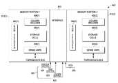
- a memorycomprising a first memory portion, a second memory portion, and an interface.
- the memory portionsin one embodiment are electrically isolated from each other. In one embodiment, this electrical isolation is achieved by physically placing the interface between the memory portions.
- the interfaceis adapted, in one embodiment, to enable it to receive a row command and a column command in the time it takes to cycle the memory once (to read one base granularity of data out of or write one base granularity of data into the memory).
- the interfaceis adapted, in one embodiment, to enable it to receive a row command and a column command in the time it takes to cycle the memory once (to read one base granularity of data out of or write one base granularity of data into the memory).
- full data bus utilizationis achieved by interleaving access requests between the two memory portions. More specifically, the interface receives a first access request (comprising a row command and no more than one column command) on a set of control ports, and forwards the request on to the first memory portion for processing. In response, the first memory portion accesses a first set of data having a size of no more than one base granularity, and sends that data onto a data bus (assuming a read operation). A data set is thus extracted from the memory. Thereafter, the interface receives a second access request on the same set of control ports, and forwards the request to the second memory portion for processing.
- a first access requestcomprising a row command and no more than one column command
- the second memory portionaccesses a second set of data also having a size of no more than one base granularity, and sends that data onto the data bus. If the access requests are timed properly relative to each other, then the second set of data will be sent onto the data bus immediately after the first set of data such that there is substantially no idle time on the data bus. With no data bus idle time, full data bus utilization is achieved. This full data bus utilization may be perpetually maintained by continuously interleaving access requests between the two portions.
- proper relative timing between the various access requestsis made possible, as least partially, by the fact that the memory portions are electrically isolated from each other, and hence, may be independently manipulated, and by the fact that a row command and a column command can be received by the interface in the time it takes to cycle either memory portion once.
- full data bus utilizationis achieved without increasing data granularity. More specifically, notice that burst mode does not need to be implemented, and that no more than one base granularity of data is sent onto the data bus in response to each access request. In addition, notice that full data bus utilization is achieved without implementing multiple memories. The different memory portions may behave like independent memories, but they are both part of the same memory using the same set of control ports. Thus, multiple memories need not be implemented. By achieving full data bus utilization without increasing data granularity and without implementing multiple memories, the present invention provides a significant advance over the prior art.
- FIG. 1is a functional diagram of a typical DRAM.
- FIG. 2is a timing diagram illustrating the steps carried out by the DRAM of FIG. 1 during several read cycles.
- FIG. 3is a timing diagram illustrating the steps carried out during several burst mode read cycles.
- FIG. 4is a block diagram of a sample multi-bank DRAM.
- FIG. 5is a timing diagram illustrating the operation of the DRAM of FIG. 4 during several read cycles.
- FIG. 6is a block diagram of a multiple DRAM implementation.
- FIG. 7is a timing diagram illustrating the operation of the implementation shown in FIG. 6 during several read cycles.
- FIG. 8is a block diagram of a system in which one embodiment of the present invention may be implemented.
- FIG. 9is a detailed block diagram of a memory in accordance with one embodiment of the present invention.
- FIG. 10is a timing diagram illustrating the operation of the memory shown in FIG. 9 during several read cycles.
- FIG. 11is a timing diagram illustrating an alternative operation of the memory of FIG. 9 wherein a single set of control ports/lines is used to send both row and column commands.
- FIG. 12is a flow diagram illustrating the operation of the memory controller of FIG. 8 in accordance with one embodiment of the present invention.
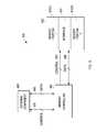
- FIG. 8there is shown a block diagram of a system 800 in which one embodiment of the present invention may be implemented, the system 800 comprising a memory 802 , a memory controller 804 , and an external component 806 .
- memory 802is a dynamic random access memory (DRAM).
- DRAMdynamic random access memory
- memory 802is implemented as an integrated circuit.
- the external component 806(which may, for example, be a CPU executing a program) is the component that requires access to the memory 802 for purposes of writing data into the memory 802 , reading data out of the memory 802 , or both.
- the external component 806submits requests to the memory controller 804 via a set of control 830 and data lines 832 .
- the memory controller 804translates the requests into access requests that the memory 802 can understand, and sends the access requests to the memory 802 via another set of control 822 and data lines 820 .
- datais provided to the memory 802 via the data lines 820 .
- a readdata is provided by the memory 802 to the controller 804 via the data lines 820 .
- the interface 810 of the memory 802receives the access requests from the controller 804 and responds by accessing the memory portions 812 ( 1 ), 812 ( 2 ) of the memory 802 .
- the interface 810accesses whichever portion 812 ( 1 ), 812 ( 2 ) is indicated in an access request. Since it is the controller 804 that generates the access requests, it is the controller 804 that controls which portions 812 ( 1 ), 812 ( 2 ) of the memory 802 are accessed and in what sequence. As will be discussed in a later section, it is desirable to interleave access requests between the different portions 812 ( 1 ), 812 ( 2 ) to achieve full data bus utilization.
- the controller 804Since it is the controller 804 that controls which memory portions 812 ( 1 ), 812 ( 2 ) are accessed, it is up to the controller 804 to properly interleave the access requests between the portions 812 ( 1 ), 812 ( 2 ) to enable full data bus utilization. The operation of the controller 804 will be described in greater detail in a later section.
- the memory 802is depicted as comprising two portions 812 ( 1 ), 812 ( 2 ). It should be noted that this is for illustrative purposes only. If so desired, the memory 802 may be implemented with any number of portions.
- Each portion 812may comprise one or more banks. In the following description, for the sake of simplicity, it will be assumed that each portion 812 comprises one bank. However, it should be noted that for purposes of the present invention, each portion 812 may comprise 1 to n banks, where n is any integer.
- the memory 802comprises an interface 810 , and two memory portions 812 ( 1 ), 812 ( 2 ).
- the first memory portion 812 ( 1 )comprises a bank with a plurality of memory/storage cells 902 ( 1 ) arranged in rows and columns, and a row decoder 904 ( 1 ) and column decoder 906 ( 1 ) for facilitating access to the memory cells 902 ( 1 ).
- the first memory portion 812 ( 1 )comprises a set of sense amps 908 ( 1 ) coupled to a data bus 820 for receiving data therefrom and sending data thereto.
- the second memory portion 812 ( 2 )comprises a bank with a plurality of memory/storage cells 902 ( 2 ) arranged in rows and columns, and a row decoder 904 ( 2 ) and column decoder 906 ( 2 ) for facilitating access to the memory cells 902 ( 2 ).
- the second memory portion 812 ( 2 )comprises a set of sense amps 908 ( 2 ) coupled to the data bus 820 for receiving data therefrom and sending data thereto.
- the memory portions 812 ( 1 ), 812 ( 2 )may be treated like independent memories. That is, each portion 812 may be accessed independently of the other portion 812 from a timing standpoint. More specifically, portion 812 ( 1 ) may be accessed at any time relative to the accessing of portion 812 ( 2 ), and portion 812 ( 2 ) may be accessed at any time relative to the accessing of portion 812 ( 1 ). Put another way, no timing constraint is imposed on when one portion may be accessed relative to the other. Thus, there is no minimum required time delay between accessing one portion 812 ( 1 ) and accessing the other portion 812 ( 2 ).
- the memory portions 812greatly facilitates the process of interleaving access requests between the portions 812 ( 1 ), 812 ( 2 ) to achieve full data bus utilization without increasing data granularity.
- the memory portions 812 ( 1 ), 812 ( 2 )may be treated like independent memories from an accessing point of view, they are still part of the same memory 802 . They share the same data bus 820 , the same interface 810 , and the same control ports/lines 822 .
- the memory 802is a single memory, not multiple, separate memories.
- the independent nature of the memory portions 812is derived from that fact that they are electrically isolated from each other.
- electrically isolatedit is meant that the two portions 812 ( 1 ), 812 ( 2 ) are sufficiently decoupled from each other from an electrical noise standpoint that the access of one portion does not corrupt data in the other portion.
- the activation of one set of sense amps 908does not corrupt data in the other set of sense amps 908 , regardless of the timing of the activations.
- the electrical isolation between the memory portions 812 ( 1 ), 812 ( 2 )is achieved by physically placing the interface 810 between the two portions 812 ( 1 ), 812 ( 2 ).
- the interface 810provides a natural and convenient barrier between the two portions 812 ( 1 ), 812 ( 2 ) and works effectively to electrically isolate one portion 812 ( 1 ) from the other 812 ( 2 ). It should be noted that this is just one possible way of achieving electrical isolation between the portions 812 ( 1 ), 812 ( 2 ). The same result may be achieved in many other ways (e.g. improved sense amp circuits, better power supply control, circuit enhancements, etc.). All such means for electrically isolating the portions 812 ( 1 ), 812 ( 2 ) are within the scope of the present invention.
- both memory portions 812 ( 1 ), 812 ( 2 )share the interface 810 and the control ports/lines 822 .
- the interface 810receives all access requests via the control ports/lines 822 and forwards the requests on to the proper memory portion 812 ( 1 ), 812 ( 2 ) for processing.
- the interface 810acts as a manager to manage the processing of access requests by the memory portions 812 ( 1 ), 812 ( 2 ).
- the interface 810receives several sets of information on the control ports/lines 822 from the controller 804 for each access request.
- these sets of informationinclude: (1) portion selection information 924 that specifies which memory portion 812 ( 1 ), 812 ( 2 ) is to be accessed; (2) row control information 920 that specifies which row of storage cells within a memory portion is to be accessed; and (3) column control information 922 that specifies which column or columns of storage cells within that row are to be accessed. Together, these sets of information provide all of the information needed to access one base granularity of data from one of the portions 812 ( 1 ), 812 ( 2 ) of the memory 802 .
- the row control information 920may take the form of a row command (e.g. comprising a row address and a RAS) sent as a set of parallel bits, or it may take the form of a row command sent as a serialized packet, or it may take any other form. So long as sufficient information is provided to the interface 810 to instruct the interface 810 to access a particular row of storage cells, any row command format may be used. The same is true for the column control information 922 . Specifically, the column control information 922 may take the form of a column command (e.g.
- any column command formatmay be used.
- the interface 810manages the operation of the memory portions 812 ( 1 ), 812 ( 2 ).
- the interface 810is capable of receiving both a row command and a column command from the controller 804 in an amount of time X, where X is less than or equal to the amount of time T it takes to cycle either of the memory portions 812 ( 1 ), 812 ( 2 ) once.
- the amount of time T it takes to cycle the memory 802is the amount of time needed to read one base granularity of data out of, or write one base granularity of data into either portion 812 ( 1 ), 812 ( 2 ) of the memory 802 .
- the base granularity of the memory 802refers to the amount of data that is read out of or written into the memory 802 in response to each column command (when no burst mode is implemented).
- the interface 810greatly facilitates the process of achieving full data bus utilization without increasing data granularity.
- the row command and the column command received by the interface 810 in the amount of time Xmay correspond to different access requests due to the process of pipelining.
- FIG. 10shows eight read access requests interleaved between the two portions 812 ( 1 ), 812 ( 2 ).
- FIG. 10shows only read cycles.
- write operationsmay be carried out in a similar fashion.
- the following nomenclaturewill be used in FIG.
- P 1will be used to indicate an access request to the first portion 812 ( 1 ) of the memory, while P 2 will be used to indicate an access request to the second portion 812 ( 2 );
- Row 1will be used to indicate a row command to portion 812 ( 1 ), while Row 2 will be used to indicate a row command to portion 812 ( 2 );
- Col 1will be used to indicate a column command to portion 812 ( 1 ), while Col 2 will be used to indicate a column command to portion 812 ( 2 ).
- the interface 810receives a first access request from the controller 804 to read a set of data from the first portion 812 ( 1 ) of the memory 802 .
- This first access requestcomprises a portion indication 1002 ( 1 ) sent on the portion control port/line 924 , a row command 1004 ( 1 ) sent on the row control ports/lines 920 , and a column command 1006 ( 1 ) sent on the column control ports/lines 922 .
- the row command 1004 ( 1 )is sent first and the column command 1006 ( 1 ) is sent later.
- SDRAMsynchronous DRAM
- the row command 1004 ( 1 ) and the column command 1006 ( 1 )may be sent in consecutive clock cycles.
- the interface 810determines that it is intended for the first memory portion 812 ( 1 ); hence, it forwards the row command 1004 ( 1 ) and the subsequent column command 1006 ( 1 ) on to portion 812 ( 1 ).
- the row decoder 904 ( 1 ) of the first memory portion 812 ( 1 )decodes the row address contained in the row command 1004 ( 1 ). This causes one of the rows of storage cells 902 ( 1 ) to be accessed, and the data contained therein to be loaded into the sense amps 908 ( 1 ).
- the column decoder 906 ( 1 ) of the first portion 812 ( 1 )decodes the column address contained in the column command 1006 ( 1 ), which causes a subset of the data contained in the sense amps 908 ( 1 ) to be sent onto the data bus 820 .
- This output data 1008 ( 1 )appears on the data bus 820 a short time after the first access request is received, and is one base granularity in size (because the access request contained only one column command and burst mode was not implemented). A first set of data 1008 ( 1 ) is thus extracted from the memory 802 .
- the interface 810receives a second access request from the controller 804 to read a set of data from the second portion 812 ( 2 ) of the memory 802 .
- This second access requestcomprises a portion indication 1002 ( 2 ) sent on the portion control port/line 924 , a row command 1004 ( 2 ) sent on the row control ports/lines 920 , and a column command 1006 ( 2 ) sent on the column control ports/lines 922 .
- the row command 1004 ( 2 )is sent first and the column command 1006 ( 2 ) is sent later. Notice from the embodiment shown in FIG.
- both the row command 1004 ( 2 ) and the column command 1006 ( 1 )are received in an amount of time X, which is less than or equal to the time T needed to cycle either of the memory portions 812 ( 1 ), 812 ( 2 ) once.
- the ability of the controller 804 to send, and the ability of the interface 810 to receive, both a row command and a column command in an amount of time X less than or equal to Tcontributes to the system's ability to achieve full data bus utilization without increasing data granularity.
- the row command 1004 ( 2 ) of the second access requestis received immediately after the row command 1004 ( 1 ) of the first access request. There is no required minimum time delay between the two commands 1004 ( 1 ), 1004 ( 2 ).
- the row commands 1004 ( 1 ), 1004 ( 2 )may be received in consecutive clock cycles. In one embodiment, this is made possible by the fact that the two memory portions 812 ( 1 ), 812 ( 2 ) are electrically isolated from each other, and hence, may be treated like independent memories.
- the two memory portions 812 ( 1 ), 812 ( 2 )may be treated like independent memories, it is possible to receive and forward an access request to one of the memory portions 812 ( 1 ), 812 ( 1 ) without regard to the other. This in turn means that there is no timing restriction on when a row command may be sent to one memory portion relative to a row command being sent to the other memory portion. As will be discussed further below, this lack of a timing constraint between the row commands facilitates the process of achieving full data bus utilization without increasing data granularity.
- the interface 810Upon receiving the second access request, the interface 810 determines that it is intended for the second memory portion 812 ( 2 ); hence, it forwards the request on to portion 812 ( 2 ). In response, the row decoder 904 ( 2 ) of the second memory portion 812 ( 2 ) decodes the row address contained in the row command 1004 ( 2 ). This causes one of the rows of storage cells 902 ( 2 ) to be accessed, and the data contained therein to be loaded into the sense amps 908 ( 2 ).
- the column decoder 906 ( 2 ) of the second portion 812 ( 2 )decodes the column address contained in the column command 1006 ( 2 ), which causes a subset of the data contained in the sense amps 908 ( 2 ) to be sent onto the data bus 820 .
- This output data 1008 ( 2 )appears on the data bus 820 a short time after the second access request is received, and like the first set of data 1008 ( 1 ), is one base granularity in size.
- the second set of data 1008 ( 2 )will be sent onto the data bus 820 immediately after the first set of data 1008 ( 1 ) so that there is substantially no idle time between the data sets 1008 ( 1 ), 1008 ( 2 ). With no data bus idle time between the data sets 1008 ( 1 ), 1008 ( 2 ), full data bus utilization is achieved.
- the interface 810receives a third access request, this one being directed back to the first memory portion 812 ( 1 ).
- the third access requestcomprises a portion indication 1002 ( 3 ), a row command 1004 ( 3 ), and a column command 1006 ( 3 ).
- the row command 1004 ( 3 )is received first and the column command 1006 ( 3 ) is received later.
- the row command 1004 ( 3 )is received immediately after the row command 1004 ( 2 ) of the second access request and is received concurrently with the column command 1006 ( 2 ) of the second access request.
- the row command 1006 ( 3 ) and the column command 1006 ( 2 )are received in an amount of time X, which is less than or equal to the amount of time T needed to cycle either of the memory portions 812 ( 1 ), 812 ( 2 ) once.
- the interface 810Upon receiving this third access request, the interface 810 determines that it is intended for the first memory portion 812 ( 1 ); hence, it forwards the request on to portion 812 ( 1 ).
- the row decoder 904 ( 1 ) and the column decoder 906 ( 1 ) of the first portion 812 ( 1 )decode the row address and the column address contained in the row command 1006 ( 3 ) and column command 1006 ( 3 ), respectively, and cause a base granularity of data to be sent from the sense amps 908 ( 1 ) onto the data bus 820 (in the manner already described).
- This output data 1008 ( 3 )appears on the data bus 820 a short time after the third access request is received, and like the first two sets of data 1008 ( 1 ), 1008 ( 2 ), is one base granularity in size. If the third access request is properly timed relative to the second access request, then the third set of data 1008 ( 3 ) will be sent onto the data bus 820 immediately after the second set of data 1008 ( 2 ). Thus, there is substantially no idle time between the data sets 1008 ( 2 ), 1008 ( 3 ), which in turn enables full data bus utilization to be achieved.
- the interface 810receives a fourth access request, this one being directed back to the second memory portion 812 ( 2 ).
- the fourth access requestcomprises a portion indication 1002 ( 4 ), a row command 1004 ( 4 ), and a column command 1006 ( 4 ).
- the row command 1004 ( 4 )is received first and the column command 1006 ( 4 ) is received later.
- the row command 1004 ( 4 )is received immediately after the row command 1004 ( 3 ) of the third access request and is received concurrently with the column command 1006 ( 3 ) of the third access request.
- the row command 1006 ( 4 ) and the column command 1006 ( 3 )are received in an amount of time X, which is less than or equal to the amount of time T needed to cycle either of the memory portions 812 ( 1 ), 812 ( 2 ) once.
- the interface 810Upon receiving this fourth access request, the interface 810 determines that it is intended for the second memory portion 812 ( 2 ); hence, it forwards the request on to portion 812 ( 2 ). In response, the row decoder 904 ( 2 ) and the column decoder 906 ( 2 ) of the second portion 812 ( 2 ) decode the row address and the column address contained in the row command 1006 ( 4 ) and column command 1006 ( 4 ), respectively, and cause a base granularity of data to be sent from the sense amps 908 ( 2 ) onto the data bus 820 (in the manner already described).
- This output data 1008 ( 4 )appears on the data bus 820 a short time after the third access request is received, and like the previous sets of data 1008 ( 1 ), 1008 ( 2 ), 1008 ( 3 ), is one base granularity in size. If the fourth access request is properly timed relative to the third access request, then the fourth set of data 1008 ( 4 ) will be sent onto the data bus 820 immediately after the third set of data 1008 ( 3 ). Thus, there is substantially no idle time between the data sets 1008 ( 3 ), 1008 ( 4 ), which in turn enables full data bus utilization to be achieved.
- access requestsmay be continuously interleaved between the portions 812 ( 1 ), 812 ( 2 ) of the memory 802 to achieve sustained full data bus utilization, and since neither burst mode nor a multiple memory configuration is implemented, this full data bus utilization is achieved without increasing data granularity and without implementing multiple memories. Thus, full data bus utilization is achieved without the shortcomings of the prior art.
- the DRAM 402requires more time to receive a complete access request than it does to place one granularity of data 506 onto the data bus 410 . More specifically, to receive a complete access request, the DRAM 402 has to: (1) receive a RAS signal and a row address; and then (2) receive a CAS signal and a column address.
- the DRAM 402can be cycled twice, as shown. Because the DRAM 402 takes longer to receive a complete request than it does to cycle the memory once, the DRAM 402 cannot keep the data bus 410 full unless it accesses several base granularities of data in response to each access request (i.e. implements burst mode). Unfortunately, by implementing burst mode, the DRAM 402 increases its output data granularity. As discussed previously, this has undesirable consequences.
- the memory 802 of FIG. 9has no such problem. Because the controller 804 is able to send, and the interface 810 of memory 802 is able to receive, both a row command and a column command (even though they may correspond to different access requests) in the time it takes to cycle the memory 802 once, memory 802 is not required to implement burst mode. Hence, memory 802 is able to achieve full data bus utilization without increasing data granularity, as shown in FIG. 10 .
- DRAM 402has a time constraint, commonly referred to as Trr, which precludes it from receiving one RAS signal (i.e. a row command) immediately after another. More particularly, the DRAM 402 is required to wait at least a Trr period of time between successive RAS signals, even if the RAS signals are directed to different banks. This time constraint is due, at least in part, to the fact that the banks 404 ( 1 ), 404 ( 2 ) of DRAM 402 are not electrically isolated from each other.
- Trrtime constraint
- one of the sets of sense amps 408is activated.
- the activation of one of the sets of sense amps 408causes a current spike, which in turn causes electrical noise.
- the memory 902 of FIG. 9has no such problem. Because the memory portions 812 ( 1 ), 812 ( 2 ) are electrically isolated from each other, noise from one portion 812 does not affect the other. As a result, there is no required minimum time delay between successive sense amp activations in the different portions 812 , which in turn means that there is no required minimum time delay between successive interleaved row commands. As shown in FIG. 10 , interleaved row commands 1004 may be received and passed on to the different memory portions 812 in immediate succession, if so desired. By eliminating the Trr time constraint, memory 802 makes it possible to time the access requests such that data sets 1008 are placed onto the data bus 820 in immediate succession with substantially no intervening idle time. By eliminating data bus idle time, full data bus utilization is achieved. As noted previously, this is accomplished without increasing data granularity and without implementing multiple separate memories. Hence, memory 802 represents a significant improvement over the prior art.
- the operation of the system 800has been described only with reference to read operations. It should be noted, though, that the same concepts, timing, sequence of commands, and data ordering may be applied to write operations.
- the controller 804is sending data onto the data bus 820 to the memory 802 . More specifically, in a read operation, the memory 802 : (1) accesses a row of data from one of the memory portions 812 ; (2) loads that data into one of the sets of sense amps 908 ; and (3) outputs a portion of the data in the sense amps 908 onto the data bus 820 .
- the memory 802In a write operation, the memory 802 : (1) accesses a row of data from one of the memory portions 812 ; (2) loads that data into one of the sets of sense amps 908 ; (3) obtains a set of write data from the data bus 820 ; (4) loads the write data into a portion of one of the sets of sense amps 908 ; and (4) stores the data in the sense amps 908 back into the appropriate row.
- the difference between a read and a write operationresides mainly in the direction of the flow of data. With regard to the timing of the portion control signals, the row and column commands, and even the data sets on the data bus, all may remain the same as that shown in FIG. 10 for read operations. In a write operation, it will be up to the controller 804 to send the data onto the data bus 820 at the proper time.
- memory 802has been described as having separate row control 920 and column control 922 ports/lines, and as receiving row and column commands concurrently on those ports/lines. While this is one possible embodiment, it should be noted that other embodiments are also possible.
- one set of control linesmay be multiplexed to carry both the row command and the column command, as shown in the timing diagram of FIG. 11 . This may be carried out, for example, by running the single set of control lines at double speed, or by sending a row command and a column command on different halves of a clock cycle. So long as a row command and a column command can be received in the time it takes to cycle the memory 802 once, any method/configuration for supplying the row command and column command may be used/implemented.
- the memory controller 804( FIG. 8 ) that controls the accessing of data from the memory 802 .
- the controller 804controls the sending of access requests to the memory 802 , and the interleaving of access requests to the different portions 812 of the memory 802 (as shown in FIG. 10 ).
- the controller 804has the ability to send a row command and a column command to the memory 802 in an amount of time X, where X is less than or equal to the amount of time T that it takes to cycle the memory once, and has the logic for properly controlling the timing of the access requests.
- the controller 804in one embodiment implements the following rule. If two consecutive access requests are directed to different portions 812 of the memory 802 , then the access requests may be timed such that they cause the data bus 820 to be fully utilized (i.e. no data bus idle time between successive data sets, as shown in FIG. 10 ). Because the access requests are directed to different portions 812 of the memory 802 , there is no required minimum time delay between the access requests (i.e. between the row commands of the access requests).
- the controller 804imposes a delay between the row commands of the access requests, if necessary. This delay may, for example, be equal to Trr. Because the access requests will cause the same set of sense amps to be activated, this delay is implemented to prevent data errors.
- the operation of the controller 804is shown in the flow diagram of FIG. 12 .
- the controller 804receives ( 1202 ) a request from the external component 806 to access the memory 802 .
- the controller 804translates ( 1204 ) the request to derive an access request that the memory 802 can understand.
- the controller 804based upon the request, the controller 804 generates a set of portion control information, a row command, and a column command.
- the controller 804determines ( 1206 ) the memory portion 812 that needs to be accessed to service this request. If this portion 812 is determined ( 1208 ) by the controller to be the same portion as that accessed by the access request immediately preceding the current access request, then the controller 804 imposes ( 1210 ) a time delay, if necessary.
- the controller 804determines whether a certain amount of time, such as Trr, has passed since the row command of the previous access request was sent to the memory 802 . If not, then a delay is imposed to ensure that the proper amount of time has passed before sending the row command of the current access request to the memory 802 . Once the proper amount of time has passed, the controller 804 sends ( 1212 ) the current access request (comprising a row command and a subsequent column command) to the memory 802 . The controller 804 loops back to receive ( 1202 ) another request from the external component 806 .
- Trra certain amount of time
- the controller 804determines that the current access request is not directed to the same memory portion 812 as the immediately preceding access request, then it proceeds to determine ( 1214 ) the proper timing for sending the current access request relative to the previous access request. In doing so, the controller 804 (when possible) times the sending of the current access request such that it causes the memory 802 to output data onto the data bus 820 (in the case of a read operation) with substantially no idle time between data sets. By doing so, the controller 804 enables the memory 802 to achieve full data bus utilization. In some cases, it may not be possible for the controller 804 to time the requests such that full data bus utilization is achieved.
- the controller 804when there is a large time interval between requests from the external component 806 , it may not be possible for the controller 804 to send access requests which are close enough in time to achieve full data bus utilization. In such cases, the controller 804 sends the current access request immediately to the memory 802 to minimize idle time on the data bus.
- the controller 804since the current access request is directed to a different memory portion than the immediately preceding access request, the controller 804 does not need to impose any minimum time delay between the sending of the access requests. Thus, if so desired, the row command of the current access request may be sent immediately after the row command of the preceding access request. In an SDRAM, the row command of the preceding access request and the row command of the current access request may be sent in consecutive clock cycles.
- the controller 804sends ( 1212 ) the current access request to the memory 802 at the proper time to cause the memory 802 to be accessed.
- the controller 804loops back to receive ( 1202 ) another request from the external component 806 . In the manner described, the controller 804 interleaves access requests between the memory portions 812 whenever possible to enable full data bus utilization. At the same time, it imposes time delays when necessary to prevent data errors.
Landscapes
- Engineering & Computer Science (AREA)
- Theoretical Computer Science (AREA)
- Human Computer Interaction (AREA)
- Physics & Mathematics (AREA)
- General Engineering & Computer Science (AREA)
- General Physics & Mathematics (AREA)
- Computer Security & Cryptography (AREA)
- Dram (AREA)
Abstract
Description
Claims (20)
Priority Applications (6)
| Application Number | Priority Date | Filing Date | Title |
|---|---|---|---|
| US12/393,265US8370596B2 (en) | 2001-04-17 | 2009-02-26 | Mechanism for enabling full data bus utilization without increasing data granularity |
| US13/720,585US8856480B2 (en) | 2001-04-17 | 2012-12-19 | Mechanism for enabling full data bus utilization without increasing data granularity |
| US14/476,334US9257161B2 (en) | 2001-04-17 | 2014-09-03 | Mechanism for enabling full data bus utilization without increasing data granularity |
| US14/965,845US9417800B2 (en) | 2001-04-17 | 2015-12-10 | Mechanism for enabling full data bus utilization without increasing data granularity |
| US15/209,429US10146445B2 (en) | 2001-04-17 | 2016-07-13 | Mechanism for enabling full data bus utilization without increasing data granularity |
| US16/177,199US10860216B2 (en) | 2001-04-17 | 2018-10-31 | Mechanism for enabling full data bus utilization without increasing data granularity |
Applications Claiming Priority (2)
| Application Number | Priority Date | Filing Date | Title |
|---|---|---|---|
| US09/837,307US7500075B1 (en) | 2001-04-17 | 2001-04-17 | Mechanism for enabling full data bus utilization without increasing data granularity |
| US12/393,265US8370596B2 (en) | 2001-04-17 | 2009-02-26 | Mechanism for enabling full data bus utilization without increasing data granularity |
Related Parent Applications (1)
| Application Number | Title | Priority Date | Filing Date |
|---|---|---|---|
| US09/837,307DivisionUS7500075B1 (en) | 2001-04-17 | 2001-04-17 | Mechanism for enabling full data bus utilization without increasing data granularity |
Related Child Applications (1)
| Application Number | Title | Priority Date | Filing Date |
|---|---|---|---|
| US13/720,585ContinuationUS8856480B2 (en) | 2001-04-17 | 2012-12-19 | Mechanism for enabling full data bus utilization without increasing data granularity |
Publications (2)
| Publication Number | Publication Date |
|---|---|
| US20090157993A1 US20090157993A1 (en) | 2009-06-18 |
| US8370596B2true US8370596B2 (en) | 2013-02-05 |
Family
ID=40385481
Family Applications (7)
| Application Number | Title | Priority Date | Filing Date |
|---|---|---|---|
| US09/837,307Active2031-11-04US7500075B1 (en) | 2001-04-17 | 2001-04-17 | Mechanism for enabling full data bus utilization without increasing data granularity |
| US12/393,265Expired - Fee RelatedUS8370596B2 (en) | 2001-04-17 | 2009-02-26 | Mechanism for enabling full data bus utilization without increasing data granularity |
| US13/720,585Expired - Fee RelatedUS8856480B2 (en) | 2001-04-17 | 2012-12-19 | Mechanism for enabling full data bus utilization without increasing data granularity |
| US14/476,334Expired - Fee RelatedUS9257161B2 (en) | 2001-04-17 | 2014-09-03 | Mechanism for enabling full data bus utilization without increasing data granularity |
| US14/965,845Expired - Fee RelatedUS9417800B2 (en) | 2001-04-17 | 2015-12-10 | Mechanism for enabling full data bus utilization without increasing data granularity |
| US15/209,429Expired - Fee RelatedUS10146445B2 (en) | 2001-04-17 | 2016-07-13 | Mechanism for enabling full data bus utilization without increasing data granularity |
| US16/177,199Expired - Fee RelatedUS10860216B2 (en) | 2001-04-17 | 2018-10-31 | Mechanism for enabling full data bus utilization without increasing data granularity |
Family Applications Before (1)
| Application Number | Title | Priority Date | Filing Date |
|---|---|---|---|
| US09/837,307Active2031-11-04US7500075B1 (en) | 2001-04-17 | 2001-04-17 | Mechanism for enabling full data bus utilization without increasing data granularity |
Family Applications After (5)
| Application Number | Title | Priority Date | Filing Date |
|---|---|---|---|
| US13/720,585Expired - Fee RelatedUS8856480B2 (en) | 2001-04-17 | 2012-12-19 | Mechanism for enabling full data bus utilization without increasing data granularity |
| US14/476,334Expired - Fee RelatedUS9257161B2 (en) | 2001-04-17 | 2014-09-03 | Mechanism for enabling full data bus utilization without increasing data granularity |
| US14/965,845Expired - Fee RelatedUS9417800B2 (en) | 2001-04-17 | 2015-12-10 | Mechanism for enabling full data bus utilization without increasing data granularity |
| US15/209,429Expired - Fee RelatedUS10146445B2 (en) | 2001-04-17 | 2016-07-13 | Mechanism for enabling full data bus utilization without increasing data granularity |
| US16/177,199Expired - Fee RelatedUS10860216B2 (en) | 2001-04-17 | 2018-10-31 | Mechanism for enabling full data bus utilization without increasing data granularity |
Country Status (1)
| Country | Link |
|---|---|
| US (7) | US7500075B1 (en) |
Families Citing this family (29)
| Publication number | Priority date | Publication date | Assignee | Title |
|---|---|---|---|---|
| US8135795B2 (en)* | 2003-04-03 | 2012-03-13 | International Business Machines Corporation | Method to provide on-demand resource access |
| US8595459B2 (en) | 2004-11-29 | 2013-11-26 | Rambus Inc. | Micro-threaded memory |
| JP2011233114A (en)* | 2010-04-30 | 2011-11-17 | Toshiba Corp | Memory system |
| US9189675B2 (en) | 2011-04-28 | 2015-11-17 | Moon J. Kim | Adaptive fingerprint scanning |
| US8699762B2 (en) | 2011-05-13 | 2014-04-15 | Moon J. Kim | Multi-sided card having a resistive fingerprint imaging array |
| US8675928B2 (en) | 2011-06-14 | 2014-03-18 | Moon J. Kim | Multiple charge-coupled biometric sensor array |
| US20130151766A1 (en)* | 2011-12-12 | 2013-06-13 | Moon J. Kim | Convergence of memory and storage input/output in digital systems |
| US9030906B2 (en) | 2012-06-06 | 2015-05-12 | Intel Corporation | Isolating, at least in part, local row or column circuitry of memory cell before establishing voltage differential to permit reading of cell |
| US10020036B2 (en)* | 2012-12-12 | 2018-07-10 | Nvidia Corporation | Address bit remapping scheme to reduce access granularity of DRAM accesses |
| US9811453B1 (en)* | 2013-07-31 | 2017-11-07 | Juniper Networks, Inc. | Methods and apparatus for a scheduler for memory access |
| KR20150017526A (en)* | 2013-08-07 | 2015-02-17 | 삼성전자주식회사 | Memory command schedular and method for memory command scheduling |
| US9613691B2 (en) | 2015-03-27 | 2017-04-04 | Intel Corporation | Apparatus and method for drift cancellation in a memory |
| US10719237B2 (en) | 2016-01-11 | 2020-07-21 | Micron Technology, Inc. | Apparatuses and methods for concurrently accessing multiple partitions of a non-volatile memory |
| US9824767B1 (en) | 2016-06-29 | 2017-11-21 | Intel Corporation | Methods and apparatus to reduce threshold voltage drift |
| WO2018044391A1 (en) | 2016-09-02 | 2018-03-08 | Rambus Inc. | Memory component with input/output data rate alignment |
| US10782911B2 (en) | 2018-11-19 | 2020-09-22 | Micron Technology, Inc. | Data migration dynamic random access memory |
| US11182090B2 (en)* | 2018-11-19 | 2021-11-23 | Micron Technology, Inc. | Systems, devices, and methods for data migration |
| US11256437B2 (en) | 2018-11-19 | 2022-02-22 | Micron Technology, Inc. | Data migration for memory operation |
| US11163473B2 (en) | 2018-11-19 | 2021-11-02 | Micron Technology, Inc. | Systems, devices, techniques, and methods for data migration |
| KR20200126678A (en) | 2019-04-30 | 2020-11-09 | 에스케이하이닉스 주식회사 | Memory system and operating method thereof |
| KR20200126666A (en)* | 2019-04-30 | 2020-11-09 | 에스케이하이닉스 주식회사 | Memory system and operating method thereof |
| KR20200124045A (en) | 2019-04-23 | 2020-11-02 | 에스케이하이닉스 주식회사 | Memory system and operating method thereof |
| KR20200137548A (en) | 2019-05-30 | 2020-12-09 | 에스케이하이닉스 주식회사 | Memory device and test operating method thereof |
| US11139010B2 (en) | 2018-12-11 | 2021-10-05 | SK Hynix Inc. | Memory system and operating method of the memory system |
| US11404097B2 (en) | 2018-12-11 | 2022-08-02 | SK Hynix Inc. | Memory system and operating method of the memory system |
| WO2020167549A1 (en) | 2019-02-12 | 2020-08-20 | Rambus Inc. | Memory with variable access granularity |
| CN114303193A (en) | 2019-08-23 | 2022-04-08 | 拉姆伯斯公司 | Hierarchical Bank Group Timing |
| US12135901B2 (en) | 2019-08-27 | 2024-11-05 | Rambus Inc. | Joint command dynamic random access memory (DRAM) apparatus and methods |
| US12073120B2 (en)* | 2022-10-13 | 2024-08-27 | Micron Technology, Inc. | Activate information on preceding command |
Citations (79)
| Publication number | Priority date | Publication date | Assignee | Title |
|---|---|---|---|---|
| US4377855A (en) | 1980-11-06 | 1983-03-22 | National Semiconductor Corporation | Content-addressable memory |
| US4542483A (en) | 1983-12-02 | 1985-09-17 | At&T Bell Laboratories | Dual stage sense amplifier for dynamic random access memory |
| US4569036A (en) | 1982-02-26 | 1986-02-04 | Tokyo Shibaura Denki Kabushiki Kaisha | Semiconductor dynamic memory device |
| US4636982A (en) | 1984-05-04 | 1987-01-13 | Fujitsu Limited | Semiconductor memory device |
| US4646268A (en) | 1983-10-13 | 1987-02-24 | Nec Corporation | Semiconductor bipolar memory device operating in high speed |
| US4698788A (en) | 1985-07-01 | 1987-10-06 | Motorola, Inc. | Memory architecture with sub-arrays |
| US4700328A (en) | 1985-07-11 | 1987-10-13 | Intel Corporation | High speed and high efficiency layout for dram circuits |
| US4710902A (en) | 1985-10-04 | 1987-12-01 | Motorola, Inc. | Technique restore for a dynamic random access memory |
| US4740921A (en) | 1985-10-04 | 1988-04-26 | Motorola, Inc. | Precharge of a dram data line to an intermediate voltage |
| US4758993A (en) | 1984-11-19 | 1988-07-19 | Fujitsu Limited | Random access memory device formed on a semiconductor substrate having an array of memory cells divided into sub-arrays |
| US4787858A (en) | 1987-03-23 | 1988-11-29 | Digital Equipment Corporation | Latching system for computer plug |
| US4796230A (en) | 1987-06-24 | 1989-01-03 | Intel Corporation | Folded-cascode configured differential current steering column decoder circuit |
| US4800525A (en) | 1984-10-31 | 1989-01-24 | Texas Instruments Incorporated | Dual ended folded bit line arrangement and addressing scheme |
| US4811302A (en) | 1986-06-24 | 1989-03-07 | Nec Corporation | Dynamic semiconductor memory with improved sensing scheme |
| US4825413A (en) | 1987-02-24 | 1989-04-25 | Texas Instruments Incorporated | Bipolar-CMOS static ram memory device |
| US4837743A (en) | 1987-08-17 | 1989-06-06 | Texas Instruments Incorporated | Architecture for memory multiplexing |
| US4843264A (en) | 1987-11-25 | 1989-06-27 | Visic, Inc. | Dynamic sense amplifier for CMOS static RAM |
| US4862421A (en) | 1988-02-16 | 1989-08-29 | Texas Instruments Incorporated | Sensing and decoding scheme for a BiCMOS read/write memory |
| US4888732A (en) | 1987-02-23 | 1989-12-19 | Matsushita Electric Industrial Co., Ltd. | Dynamic random access memory having open bit line architecture |
| US4903344A (en) | 1987-07-07 | 1990-02-20 | Oki Electric Industry Co., Ltd. | Semiconductor memory device with staggered sense amplifiers |
| US4961168A (en) | 1987-02-24 | 1990-10-02 | Texas Instruments Incorporated | Bipolar-CMOS static random access memory device with bit line bias control |
| US4982370A (en) | 1985-10-04 | 1991-01-01 | Mitsubishi Denki Kabushiki Kaisha | Shared sense amplifier semiconductor memory |
| US4984196A (en) | 1988-05-25 | 1991-01-08 | Texas Instruments, Incorporated | High performance bipolar differential sense amplifier in a BiCMOS SRAM |
| US4991141A (en) | 1990-02-08 | 1991-02-05 | Texas Instruments Incorporated | Sense amplifier and method for sensing the outputs of static random access memory cells |
| US5046050A (en) | 1990-04-10 | 1991-09-03 | National Semiconductor Corporation | Shared BiCMOS sense amplifier |
| WO1991016680A1 (en) | 1990-04-18 | 1991-10-31 | Rambus Inc. | Integrated circuit i/o using a high preformance bus interface |
| US5093806A (en) | 1988-02-16 | 1992-03-03 | Tran Hiep V | Sensing and decoding scheme for a bicmos read/write memory |
| US5111434A (en) | 1988-12-20 | 1992-05-05 | Ltd. SamSung Electronics Co. | Semiconductor memory device |
| US5119340A (en) | 1990-09-26 | 1992-06-02 | Sgs-Thomson Microelectronics, Inc. | Semiconductor memory having latched repeaters for memory row line selection |
| US5121358A (en) | 1990-09-26 | 1992-06-09 | Sgs-Thomson Microelectronics, Inc. | Semiconductor memory with power-on reset controlled latched row line repeaters |
| US5124610A (en) | 1989-03-03 | 1992-06-23 | E. F. Johnson Company | Tritiated light emitting polymer electrical energy source |
| US5124951A (en) | 1990-09-26 | 1992-06-23 | Sgs-Thomson Microelectronics, Inc. | Semiconductor memory with sequenced latched row line repeaters |
| US5128897A (en) | 1990-09-26 | 1992-07-07 | Sgs-Thomson Microelectronics, Inc. | Semiconductor memory having improved latched repeaters for memory row line selection |
| US5132931A (en) | 1990-08-28 | 1992-07-21 | Analog Devices, Inc. | Sense enable timing circuit for a random access memory |
| US5150330A (en) | 1990-01-24 | 1992-09-22 | Vlsi Technology, Inc. | Interblock dispersed-word memory architecture |
| US5181205A (en) | 1990-04-10 | 1993-01-19 | National Semiconductor Corporation | Short circuit detector circuit for memory arrays |
| US5193072A (en) | 1990-12-21 | 1993-03-09 | Vlsi Technology, Inc. | Hidden refresh of a dynamic random access memory |
| US5193074A (en) | 1990-02-09 | 1993-03-09 | Mitsubishi Denki Kabushiki Kaisha | Semiconductor memory device having hierarchical row selecting lines |
| US5214610A (en) | 1989-09-22 | 1993-05-25 | Texas Instruments Incorporated | Memory with selective address transition detection for cache operation |
| US5222047A (en) | 1987-05-15 | 1993-06-22 | Mitsubishi Denki Kabushiki Kaisha | Method and apparatus for driving word line in block access memory |
| US5241503A (en) | 1991-02-25 | 1993-08-31 | Motorola, Inc. | Dynamic random access memory with improved page-mode performance and method therefor having isolator between memory cells and sense amplifiers |
| US5249165A (en) | 1991-03-07 | 1993-09-28 | Kabushiki Kaisha Toshiba | Memory cell array divided type multi-port semiconductor memory device |
| US5251178A (en) | 1991-03-06 | 1993-10-05 | Childers Jimmie D | Low-power integrated circuit memory |
| US5263002A (en) | 1990-06-12 | 1993-11-16 | Kabushiki Kaisha Toshiba | Semiconductor memory device and its topography |
| US5267215A (en) | 1990-11-09 | 1993-11-30 | Nec Corporation | Semiconductor memory device with transfer gates arranged to subdivide bit lines |
| US5274596A (en) | 1987-09-16 | 1993-12-28 | Kabushiki Kaisha Toshiba | Dynamic semiconductor memory device having simultaneous operation of adjacent blocks |
| US5291444A (en) | 1991-12-23 | 1994-03-01 | Texas Instruments Incorporated | Combination DRAM and SRAM memory array |
| US5301162A (en) | 1992-03-26 | 1994-04-05 | Nec Corporation | Semiconductor random access memory device having shared sense amplifiers serving as a cache memory |
| US5301278A (en) | 1988-04-29 | 1994-04-05 | International Business Machines Corporation | Flexible dynamic memory controller |
| US5305280A (en) | 1991-04-04 | 1994-04-19 | Mitsubishi Denki Kabushiki Kaisha | Semiconductor memory device having on the same chip a plurality of memory circuits among which data transfer is performed to each other and an operating method thereof |
| US5321646A (en) | 1991-04-09 | 1994-06-14 | Mitsubishi Denki Kabushiki Kaisha | Layout of a semiconductor memory device |
| US5337283A (en) | 1991-12-27 | 1994-08-09 | Nec Corporation | Dynamic random access memory device |
| US5343438A (en) | 1992-01-31 | 1994-08-30 | Samsung Electronics Co., Ltd. | Semiconductor memory device having a plurality of row address strobe signals |
| US5383159A (en) | 1992-09-17 | 1995-01-17 | Sharp Kabushiki Kaisha | Semiconductor memory device of alternately-activated open bit-line architecture |
| US5390308A (en) | 1992-04-15 | 1995-02-14 | Rambus, Inc. | Method and apparatus for address mapping of dynamic random access memory |
| US5406526A (en) | 1992-10-01 | 1995-04-11 | Nec Corporation | Dynamic random access memory device having sense amplifier arrays selectively activated when associated memory cell sub-arrays are accessed |
| US5414662A (en) | 1990-04-06 | 1995-05-09 | Mosaid Technologies Incorporated | Dynamic random access memory using imperfect isolating transistors |
| US5418737A (en) | 1990-09-17 | 1995-05-23 | Texas Instruments Incorporated | DRAM with sub data lines and match lines for test |
| US5428389A (en) | 1990-06-14 | 1995-06-27 | Fuji Photo Film Co., Ltd. | Image data storage/processing apparatus |
| US5455802A (en) | 1992-12-22 | 1995-10-03 | Sgs-Thomson Microelectronics, Inc. | Dual dynamic sense amplifiers for a memory array |
| US5471425A (en) | 1993-03-10 | 1995-11-28 | Fujitsu Limited | Dynamic random access memory having sense amplifier control circuit supplied with external sense amplifier activating signal |
| US5485430A (en) | 1992-12-22 | 1996-01-16 | Sgs-Thomson Microelectronics, Inc. | Multiple clocked dynamic sense amplifier |
| US5517456A (en) | 1993-11-02 | 1996-05-14 | Nec Corporation | Semiconductor memory device including a word line driving circuit of the divisional decoding type |
| US5587960A (en) | 1994-11-15 | 1996-12-24 | Sgs-Thomson Microelectronics Limited | Integrated circuit memory device with voltage boost |
| US5636367A (en)* | 1991-02-27 | 1997-06-03 | Vlsi Technology, Inc. | N+0.5 wait state programmable DRAM controller |
| US5903509A (en) | 1995-12-29 | 1999-05-11 | Micron Technology, Inc. | Memory device with multiple internal banks and staggered command execution |
| US5933387A (en) | 1998-03-30 | 1999-08-03 | Richard Mann | Divided word line architecture for embedded memories using multiple metal layers |
| US6034878A (en) | 1996-12-16 | 2000-03-07 | Hitachi, Ltd. | Source-clock-synchronized memory system and memory unit |
| US6075728A (en) | 1997-02-28 | 2000-06-13 | Mitsubishi Denki Kabushiki Kaisha | Semiconductor memory device accessible at high speed |
| US6240039B1 (en) | 1999-06-26 | 2001-05-29 | Samsung Electronics Co., Ltd. | Semiconductor memory device and driving signal generator therefor |
| US20010007538A1 (en)* | 1998-10-01 | 2001-07-12 | Wingyu Leung | Single-Port multi-bank memory system having read and write buffers and method of operating same |
| US20010030900A1 (en)* | 2000-03-24 | 2001-10-18 | Kabushiki Kaisha Toshiba | Synchronous semiconductor memory |
| US20010044885A1 (en)* | 1999-07-29 | 2001-11-22 | Laberge Paul A. | Processing memory requests that target memory banks |
| US6373761B1 (en)* | 1998-09-02 | 2002-04-16 | Micron Technology, Inc. | Method and apparatus for multiple row activation in memory devices |
| US6526484B1 (en) | 1998-11-16 | 2003-02-25 | Infineon Technologies Ag | Methods and apparatus for reordering of the memory requests to achieve higher average utilization of the command and data bus |
| US20030174573A1 (en) | 2002-03-13 | 2003-09-18 | Fujitsu Limited | Semiconductor memory device |
| US20040120197A1 (en) | 2002-01-11 | 2004-06-24 | Tetsujiro Kondo | Memory cell circuit, memory device, motion vector detection device, and motion compensation prediction coding device |
| US20050027929A1 (en)* | 1995-05-17 | 2005-02-03 | Monolithic System Technology, Inc. | High speed memory system |
| US20050073894A1 (en) | 2000-06-30 | 2005-04-07 | Micron Technology, Inc. | Zero latency-zero bus turnaround synchronous flash memory |
Family Cites Families (63)
| Publication number | Priority date | Publication date | Assignee | Title |
|---|---|---|---|---|
| JPS59160899A (en)* | 1982-12-09 | 1984-09-11 | セコイア・システムス・インコ−ポレ−テツド | Memory backup system |
| US4670745A (en) | 1983-11-15 | 1987-06-02 | Motorola Inc. | Video display address generator |
| FR2566950B1 (en) | 1984-06-29 | 1986-12-26 | Texas Instruments France | VIDEO IMAGE POINT PROCESSOR, VIEWING SYSTEM COMPRISING APPLICATION AND METHOD FOR IMPLEMENTING SAME |
| JPS61139866A (en) | 1984-12-11 | 1986-06-27 | Toshiba Corp | microprocessor |
| US4837465A (en) | 1985-01-16 | 1989-06-06 | Digital Equipment Corp | Single rail CMOS register array and sense amplifier circuit therefor |
| US4839796A (en)* | 1987-07-16 | 1989-06-13 | Icon International, Inc. | Static frame digital memory |
| US5146592A (en) | 1987-09-14 | 1992-09-08 | Visual Information Technologies, Inc. | High speed image processing computer with overlapping windows-div |
| JPH02168496A (en) | 1988-09-14 | 1990-06-28 | Kawasaki Steel Corp | Semiconductor memory circuit |
| JP3039557B2 (en) | 1989-11-01 | 2000-05-08 | 日本電気株式会社 | Storage device |
| JP2762138B2 (en) | 1989-11-06 | 1998-06-04 | 三菱電機株式会社 | Memory control unit |
| US5347648A (en)* | 1990-06-29 | 1994-09-13 | Digital Equipment Corporation | Ensuring write ordering under writeback cache error conditions |
| US5253214A (en) | 1991-09-27 | 1993-10-12 | Eastman Kodak Company | High-performance memory controller with application-programmable optimization |
| US5530814A (en) | 1991-10-30 | 1996-06-25 | I-Cube, Inc. | Bi-directional crossbar switch with control memory for selectively routing signals between pairs of signal ports |
| JP2836321B2 (en) | 1991-11-05 | 1998-12-14 | 三菱電機株式会社 | Data processing device |
| US5506977A (en)* | 1991-12-17 | 1996-04-09 | Dell Usa, L.P. | Method and controller for minimizing reads during partial stripe write operations to a disk drive |
| US5784377A (en)* | 1993-03-09 | 1998-07-21 | Hubbell Incorporated | Integrated digital loop carrier system with virtual tributary mapper circuit |
| US5465343A (en)* | 1993-04-30 | 1995-11-07 | Quantum Corporation | Shared memory array for data block and control program storage in disk drive |
| JPH06314264A (en) | 1993-05-06 | 1994-11-08 | Nec Corp | Self-routing cross bar switch |
| US5513156A (en)* | 1993-07-23 | 1996-04-30 | Fujitsu Limited | Library apparatus |
| JP2875476B2 (en) | 1993-12-06 | 1999-03-31 | 松下電器産業株式会社 | Semiconductor memory device |
| AU1841895A (en) | 1994-02-15 | 1995-08-29 | Rambus Inc. | Delay-locked loop |
| US5689195A (en) | 1995-05-17 | 1997-11-18 | Altera Corporation | Programmable logic array integrated circuit devices |
| US5655113A (en) | 1994-07-05 | 1997-08-05 | Monolithic System Technology, Inc. | Resynchronization circuit for a memory system and method of operating same |
| JP3176228B2 (en) | 1994-08-23 | 2001-06-11 | シャープ株式会社 | Semiconductor storage device |
| US5892900A (en)* | 1996-08-30 | 1999-04-06 | Intertrust Technologies Corp. | Systems and methods for secure transaction management and electronic rights protection |
| US5652870A (en) | 1995-04-11 | 1997-07-29 | Mitsubishi Denki Kabushiki Kaisha | Microcomputer having multiplexable input-output port |
| US5787267A (en) | 1995-06-07 | 1998-07-28 | Monolithic System Technology, Inc. | Caching method and circuit for a memory system with circuit module architecture |
| US5801985A (en) | 1995-07-28 | 1998-09-01 | Micron Technology, Inc. | Memory system having programmable control parameters |
| US5717871A (en) | 1995-08-17 | 1998-02-10 | I-Cube, Inc. | Crossbar switch with input/output buffers having multiplexed control inputs |
| JP3531891B2 (en) | 1996-01-26 | 2004-05-31 | シャープ株式会社 | Semiconductor storage device |
| US5793998A (en) | 1996-04-17 | 1998-08-11 | Digital Equipment Corporation | Method and apparatus for interconnection of multiple modules |
| US5852725A (en) | 1996-05-10 | 1998-12-22 | Yen; Juei-Hsiang | PCI/ISA bus single board computer card/CPU card and backplane using eisa bus connectors and eisa bus slots |
| US5933023A (en) | 1996-09-03 | 1999-08-03 | Xilinx, Inc. | FPGA architecture having RAM blocks with programmable word length and width and dedicated address and data lines |
| US5893927A (en) | 1996-09-13 | 1999-04-13 | International Business Machines Corporation | Memory device having programmable device width, method of programming, and method of setting device width for memory device |
| US5748554A (en) | 1996-12-20 | 1998-05-05 | Rambus, Inc. | Memory and method for sensing sub-groups of memory elements |
| US6505268B1 (en)* | 1996-12-20 | 2003-01-07 | Compaq Computer Corporation | Data distribution in a disk array |
| US6047347A (en) | 1997-02-04 | 2000-04-04 | Advanced Micro Devices, Inc. | Computer system with programmable bus size |
| US6125157A (en) | 1997-02-06 | 2000-09-26 | Rambus, Inc. | Delay-locked loop circuitry for clock delay adjustment |
| EP0887737B1 (en) | 1997-06-26 | 2003-01-22 | Hewlett-Packard Company, A Delaware Corporation | Reversible connectors |
| US5958033A (en) | 1997-08-13 | 1999-09-28 | Hewlett Packard Company | On- the-fly partitionable computer bus for enhanced operation with varying bus clock frequencies |
| US6247084B1 (en) | 1997-10-08 | 2001-06-12 | Lsi Logic Corporation | Integrated circuit with unified memory system and dual bus architecture |
| US5936885A (en) | 1998-02-23 | 1999-08-10 | Mitsubishi Denki Kabushiki Kaisha | Semiconductor memory capable of preventing erroneous inversion of data read from memory transistors |
| AU1513899A (en) | 1998-08-19 | 2000-03-14 | Boris Nikolaevich Vilkov | A system and method for identification of transformation of memory device addresses |
| US6130843A (en) | 1998-09-02 | 2000-10-10 | Micron Technology, Inc. | Method and circuit for providing a memory device having hidden row access and row precharge times |
| US6138185A (en) | 1998-10-29 | 2000-10-24 | Mcdata Corporation | High performance crossbar switch |
| WO2000029958A1 (en) | 1998-11-12 | 2000-05-25 | Boris Nikolayevich Vilkov | A system and a method for transformation of memory device addresses |
| US6311313B1 (en) | 1998-12-29 | 2001-10-30 | International Business Machines Corporation | X-Y grid tree clock distribution network with tunable tree and grid networks |
| KR100564421B1 (en) | 1998-12-31 | 2006-06-23 | 주식회사 하이닉스반도체 | Data Width Setting Circuit of Memory Element |
| KR100335504B1 (en) | 2000-06-30 | 2002-05-09 | 윤종용 | 2 Channel memory system having shared control and address bus and memory modules used therein |
| US7395399B2 (en) | 2000-08-25 | 2008-07-01 | Stmicroelectronics S.A. | Control circuit to enable high data rate access to a DRAM with a plurality of areas |
| US6546453B1 (en)* | 2000-08-31 | 2003-04-08 | Compaq Information Technologies Group, L.P. | Proprammable DRAM address mapping mechanism |
| US6738836B1 (en)* | 2000-08-31 | 2004-05-18 | Hewlett-Packard Development Company, L.P. | Scalable efficient I/O port protocol |
| US6625687B1 (en) | 2000-09-18 | 2003-09-23 | Intel Corporation | Memory module employing a junction circuit for point-to-point connection isolation, voltage translation, data synchronization, and multiplexing/demultiplexing |
| US6697888B1 (en) | 2000-09-29 | 2004-02-24 | Intel Corporation | Buffering and interleaving data transfer between a chipset and memory modules |
| US7246369B1 (en)* | 2000-12-27 | 2007-07-17 | Info Valve Computing, Inc. | Broadband video distribution system using segments |
| US6618795B2 (en)* | 2001-01-24 | 2003-09-09 | Sony Corporation | Method and apparatus for concurrent access to a sequential device |
| US6889304B2 (en) | 2001-02-28 | 2005-05-03 | Rambus Inc. | Memory device supporting a dynamically configurable core organization |
| TW561485B (en) | 2001-03-22 | 2003-11-11 | Fujitsu Ltd | Semiconductor memory device and information processing system |
| US6825841B2 (en) | 2001-09-07 | 2004-11-30 | Rambus Inc. | Granularity memory column access |
| US6754120B1 (en) | 2003-02-11 | 2004-06-22 | Rambus Inc. | DRAM output circuitry supporting sequential data capture to reduce core access times |
| US7266661B2 (en)* | 2004-05-27 | 2007-09-04 | Silverbrook Research Pty Ltd | Method of storing bit-pattern in plural devices |
| US7106636B2 (en) | 2004-06-22 | 2006-09-12 | Intel Corporation | Partitionable memory device, system, and method |
| JP2012068936A (en)* | 2010-09-24 | 2012-04-05 | Toshiba Corp | Memory system |
- 2001
- 2001-04-17USUS09/837,307patent/US7500075B1/enactiveActive
- 2009
- 2009-02-26USUS12/393,265patent/US8370596B2/ennot_activeExpired - Fee Related
- 2012
- 2012-12-19USUS13/720,585patent/US8856480B2/ennot_activeExpired - Fee Related
- 2014
- 2014-09-03USUS14/476,334patent/US9257161B2/ennot_activeExpired - Fee Related
- 2015
- 2015-12-10USUS14/965,845patent/US9417800B2/ennot_activeExpired - Fee Related
- 2016
- 2016-07-13USUS15/209,429patent/US10146445B2/ennot_activeExpired - Fee Related
- 2018
- 2018-10-31USUS16/177,199patent/US10860216B2/ennot_activeExpired - Fee Related
Patent Citations (79)
| Publication number | Priority date | Publication date | Assignee | Title |
|---|---|---|---|---|
| US4377855A (en) | 1980-11-06 | 1983-03-22 | National Semiconductor Corporation | Content-addressable memory |
| US4569036A (en) | 1982-02-26 | 1986-02-04 | Tokyo Shibaura Denki Kabushiki Kaisha | Semiconductor dynamic memory device |
| US4646268A (en) | 1983-10-13 | 1987-02-24 | Nec Corporation | Semiconductor bipolar memory device operating in high speed |
| US4542483A (en) | 1983-12-02 | 1985-09-17 | At&T Bell Laboratories | Dual stage sense amplifier for dynamic random access memory |
| US4636982A (en) | 1984-05-04 | 1987-01-13 | Fujitsu Limited | Semiconductor memory device |
| US4800525A (en) | 1984-10-31 | 1989-01-24 | Texas Instruments Incorporated | Dual ended folded bit line arrangement and addressing scheme |
| US4758993A (en) | 1984-11-19 | 1988-07-19 | Fujitsu Limited | Random access memory device formed on a semiconductor substrate having an array of memory cells divided into sub-arrays |
| US4698788A (en) | 1985-07-01 | 1987-10-06 | Motorola, Inc. | Memory architecture with sub-arrays |
| US4700328A (en) | 1985-07-11 | 1987-10-13 | Intel Corporation | High speed and high efficiency layout for dram circuits |
| US4982370A (en) | 1985-10-04 | 1991-01-01 | Mitsubishi Denki Kabushiki Kaisha | Shared sense amplifier semiconductor memory |
| US4710902A (en) | 1985-10-04 | 1987-12-01 | Motorola, Inc. | Technique restore for a dynamic random access memory |
| US4740921A (en) | 1985-10-04 | 1988-04-26 | Motorola, Inc. | Precharge of a dram data line to an intermediate voltage |
| US4811302A (en) | 1986-06-24 | 1989-03-07 | Nec Corporation | Dynamic semiconductor memory with improved sensing scheme |
| US4888732A (en) | 1987-02-23 | 1989-12-19 | Matsushita Electric Industrial Co., Ltd. | Dynamic random access memory having open bit line architecture |
| US4825413A (en) | 1987-02-24 | 1989-04-25 | Texas Instruments Incorporated | Bipolar-CMOS static ram memory device |
| US4961168A (en) | 1987-02-24 | 1990-10-02 | Texas Instruments Incorporated | Bipolar-CMOS static random access memory device with bit line bias control |
| US4787858A (en) | 1987-03-23 | 1988-11-29 | Digital Equipment Corporation | Latching system for computer plug |
| US5222047A (en) | 1987-05-15 | 1993-06-22 | Mitsubishi Denki Kabushiki Kaisha | Method and apparatus for driving word line in block access memory |
| US4796230A (en) | 1987-06-24 | 1989-01-03 | Intel Corporation | Folded-cascode configured differential current steering column decoder circuit |
| US4903344A (en) | 1987-07-07 | 1990-02-20 | Oki Electric Industry Co., Ltd. | Semiconductor memory device with staggered sense amplifiers |
| US4837743A (en) | 1987-08-17 | 1989-06-06 | Texas Instruments Incorporated | Architecture for memory multiplexing |
| US5274596A (en) | 1987-09-16 | 1993-12-28 | Kabushiki Kaisha Toshiba | Dynamic semiconductor memory device having simultaneous operation of adjacent blocks |
| US4843264A (en) | 1987-11-25 | 1989-06-27 | Visic, Inc. | Dynamic sense amplifier for CMOS static RAM |
| US4862421A (en) | 1988-02-16 | 1989-08-29 | Texas Instruments Incorporated | Sensing and decoding scheme for a BiCMOS read/write memory |
| US5093806A (en) | 1988-02-16 | 1992-03-03 | Tran Hiep V | Sensing and decoding scheme for a bicmos read/write memory |
| US5301278A (en) | 1988-04-29 | 1994-04-05 | International Business Machines Corporation | Flexible dynamic memory controller |
| US4984196A (en) | 1988-05-25 | 1991-01-08 | Texas Instruments, Incorporated | High performance bipolar differential sense amplifier in a BiCMOS SRAM |
| US5111434A (en) | 1988-12-20 | 1992-05-05 | Ltd. SamSung Electronics Co. | Semiconductor memory device |
| US5124610A (en) | 1989-03-03 | 1992-06-23 | E. F. Johnson Company | Tritiated light emitting polymer electrical energy source |
| US5214610A (en) | 1989-09-22 | 1993-05-25 | Texas Instruments Incorporated | Memory with selective address transition detection for cache operation |
| US5150330A (en) | 1990-01-24 | 1992-09-22 | Vlsi Technology, Inc. | Interblock dispersed-word memory architecture |
| US4991141A (en) | 1990-02-08 | 1991-02-05 | Texas Instruments Incorporated | Sense amplifier and method for sensing the outputs of static random access memory cells |
| US5193074A (en) | 1990-02-09 | 1993-03-09 | Mitsubishi Denki Kabushiki Kaisha | Semiconductor memory device having hierarchical row selecting lines |
| US5414662A (en) | 1990-04-06 | 1995-05-09 | Mosaid Technologies Incorporated | Dynamic random access memory using imperfect isolating transistors |
| US5046050A (en) | 1990-04-10 | 1991-09-03 | National Semiconductor Corporation | Shared BiCMOS sense amplifier |
| US5181205A (en) | 1990-04-10 | 1993-01-19 | National Semiconductor Corporation | Short circuit detector circuit for memory arrays |
| WO1991016680A1 (en) | 1990-04-18 | 1991-10-31 | Rambus Inc. | Integrated circuit i/o using a high preformance bus interface |
| US5263002A (en) | 1990-06-12 | 1993-11-16 | Kabushiki Kaisha Toshiba | Semiconductor memory device and its topography |
| US5428389A (en) | 1990-06-14 | 1995-06-27 | Fuji Photo Film Co., Ltd. | Image data storage/processing apparatus |
| US5132931A (en) | 1990-08-28 | 1992-07-21 | Analog Devices, Inc. | Sense enable timing circuit for a random access memory |
| US5418737A (en) | 1990-09-17 | 1995-05-23 | Texas Instruments Incorporated | DRAM with sub data lines and match lines for test |
| US5119340A (en) | 1990-09-26 | 1992-06-02 | Sgs-Thomson Microelectronics, Inc. | Semiconductor memory having latched repeaters for memory row line selection |
| US5121358A (en) | 1990-09-26 | 1992-06-09 | Sgs-Thomson Microelectronics, Inc. | Semiconductor memory with power-on reset controlled latched row line repeaters |
| US5128897A (en) | 1990-09-26 | 1992-07-07 | Sgs-Thomson Microelectronics, Inc. | Semiconductor memory having improved latched repeaters for memory row line selection |
| US5124951A (en) | 1990-09-26 | 1992-06-23 | Sgs-Thomson Microelectronics, Inc. | Semiconductor memory with sequenced latched row line repeaters |
| US5267215A (en) | 1990-11-09 | 1993-11-30 | Nec Corporation | Semiconductor memory device with transfer gates arranged to subdivide bit lines |
| US5193072A (en) | 1990-12-21 | 1993-03-09 | Vlsi Technology, Inc. | Hidden refresh of a dynamic random access memory |
| US5241503A (en) | 1991-02-25 | 1993-08-31 | Motorola, Inc. | Dynamic random access memory with improved page-mode performance and method therefor having isolator between memory cells and sense amplifiers |
| US5636367A (en)* | 1991-02-27 | 1997-06-03 | Vlsi Technology, Inc. | N+0.5 wait state programmable DRAM controller |
| US5251178A (en) | 1991-03-06 | 1993-10-05 | Childers Jimmie D | Low-power integrated circuit memory |
| US5249165A (en) | 1991-03-07 | 1993-09-28 | Kabushiki Kaisha Toshiba | Memory cell array divided type multi-port semiconductor memory device |
| US5305280A (en) | 1991-04-04 | 1994-04-19 | Mitsubishi Denki Kabushiki Kaisha | Semiconductor memory device having on the same chip a plurality of memory circuits among which data transfer is performed to each other and an operating method thereof |
| US5321646A (en) | 1991-04-09 | 1994-06-14 | Mitsubishi Denki Kabushiki Kaisha | Layout of a semiconductor memory device |
| US5291444A (en) | 1991-12-23 | 1994-03-01 | Texas Instruments Incorporated | Combination DRAM and SRAM memory array |
| US5337283A (en) | 1991-12-27 | 1994-08-09 | Nec Corporation | Dynamic random access memory device |
| US5343438A (en) | 1992-01-31 | 1994-08-30 | Samsung Electronics Co., Ltd. | Semiconductor memory device having a plurality of row address strobe signals |
| US5301162A (en) | 1992-03-26 | 1994-04-05 | Nec Corporation | Semiconductor random access memory device having shared sense amplifiers serving as a cache memory |
| US5390308A (en) | 1992-04-15 | 1995-02-14 | Rambus, Inc. | Method and apparatus for address mapping of dynamic random access memory |
| US5383159A (en) | 1992-09-17 | 1995-01-17 | Sharp Kabushiki Kaisha | Semiconductor memory device of alternately-activated open bit-line architecture |
| US5406526A (en) | 1992-10-01 | 1995-04-11 | Nec Corporation | Dynamic random access memory device having sense amplifier arrays selectively activated when associated memory cell sub-arrays are accessed |
| US5455802A (en) | 1992-12-22 | 1995-10-03 | Sgs-Thomson Microelectronics, Inc. | Dual dynamic sense amplifiers for a memory array |
| US5485430A (en) | 1992-12-22 | 1996-01-16 | Sgs-Thomson Microelectronics, Inc. | Multiple clocked dynamic sense amplifier |
| US5471425A (en) | 1993-03-10 | 1995-11-28 | Fujitsu Limited | Dynamic random access memory having sense amplifier control circuit supplied with external sense amplifier activating signal |
| US5517456A (en) | 1993-11-02 | 1996-05-14 | Nec Corporation | Semiconductor memory device including a word line driving circuit of the divisional decoding type |
| US5587960A (en) | 1994-11-15 | 1996-12-24 | Sgs-Thomson Microelectronics Limited | Integrated circuit memory device with voltage boost |
| US20050027929A1 (en)* | 1995-05-17 | 2005-02-03 | Monolithic System Technology, Inc. | High speed memory system |
| US5903509A (en) | 1995-12-29 | 1999-05-11 | Micron Technology, Inc. | Memory device with multiple internal banks and staggered command execution |
| US6034878A (en) | 1996-12-16 | 2000-03-07 | Hitachi, Ltd. | Source-clock-synchronized memory system and memory unit |
| US6075728A (en) | 1997-02-28 | 2000-06-13 | Mitsubishi Denki Kabushiki Kaisha | Semiconductor memory device accessible at high speed |
| US5933387A (en) | 1998-03-30 | 1999-08-03 | Richard Mann | Divided word line architecture for embedded memories using multiple metal layers |
| US6373761B1 (en)* | 1998-09-02 | 2002-04-16 | Micron Technology, Inc. | Method and apparatus for multiple row activation in memory devices |
| US20010007538A1 (en)* | 1998-10-01 | 2001-07-12 | Wingyu Leung | Single-Port multi-bank memory system having read and write buffers and method of operating same |
| US6526484B1 (en) | 1998-11-16 | 2003-02-25 | Infineon Technologies Ag | Methods and apparatus for reordering of the memory requests to achieve higher average utilization of the command and data bus |
| US6240039B1 (en) | 1999-06-26 | 2001-05-29 | Samsung Electronics Co., Ltd. | Semiconductor memory device and driving signal generator therefor |
| US20010044885A1 (en)* | 1999-07-29 | 2001-11-22 | Laberge Paul A. | Processing memory requests that target memory banks |
| US20010030900A1 (en)* | 2000-03-24 | 2001-10-18 | Kabushiki Kaisha Toshiba | Synchronous semiconductor memory |
| US20050073894A1 (en) | 2000-06-30 | 2005-04-07 | Micron Technology, Inc. | Zero latency-zero bus turnaround synchronous flash memory |
| US20040120197A1 (en) | 2002-01-11 | 2004-06-24 | Tetsujiro Kondo | Memory cell circuit, memory device, motion vector detection device, and motion compensation prediction coding device |
| US20030174573A1 (en) | 2002-03-13 | 2003-09-18 | Fujitsu Limited | Semiconductor memory device |
Non-Patent Citations (17)
| Title |
|---|
| Aimoto, Yashiharu, et al., "SP23.3 A 7168GIPS 3.84GB/s 1W Parallel Image-Processing RAM Integrating a 16Mb DRAM and 128 Processors", ISSCC, Feb. 1996, pp. 372-373/476. |
| Giacalone et al., "SP23.2: A 1MB, 100MHz Integrated L2 Cache Memory with 128b Interface and ECC Protection," IEEE ISSCC, Feb. 1996, pp. 370-371/475. |
| Hirose, Toshihiko, et al., "A 20-ns 4-Mb CMOS SRAM with Hierarchical Word Decoding Architecture", IEEE, Oct. 1990, pp. 1068-1072, vol. 25, No. 5. |
| JEDEC, "Minutes of Meeting No. 71, JC-42.3 Committee on RAM Memories, including Proposal to Add Number of Banks Option to the Mode Register for 64M SDRAM," Joint Electron Device Engineering Council (JEDEC), May 25, 1994, New York, pp. 1-14 plus Attachment T. |
| Koike, Hiroke et al., "SP23.1: A 60ns 1Mb Nonvolatile Ferroelectric Memory with Non-Driven Cell Plate Line Write/Read Scheme", ISSCC, Feb. 1996, pp. 368-379/475. |
| Konishi, Saisohi, et al., "Session SVIII: Static RAMs-FAM18.6: A 64Kb COMOS RAM", ISSCC, Feb. 1982, pp. 258-259/333. |
| Micron, "Graphics DDR3 DRAM." Advance. "256 Mb×32 GDDR3 DRAM." © 2003 Micron Technology, Inc. pp. 1-67. |
| Nakamura, Masayuki, et al., "FA14.2: A 29ns 64Mb DRAM with Hierarchical Array Architecture", ISSCC, Feb. 1995, pp. 246-247/373. |
| Nitta, Yasuhiko, et al., "SP23.5: A 1.6FB/s Data-Rate 1Gb Synchronous DRAM with Hierarchical Square-Shaped Memory Block & Distributed Bank Architecture", IEEE ISSCC Digest of Technical Papers, p. 376-377, 477, Feb. 10, 1996. |
| Saeki, Takanori, et al., "SP 23.4: A 2.5 ns Clock Acess 250MHz 256Mb SDRAM with a Synchronous Mirror Delay," IEEE ISSCC Digest of Technical Papers, p. 374-375, 476, Feb. 10, 1996. |
| Sakata et al., "Two-Dimensional Power-Line Selection Scheme for Low Subthreshold-Current Multi-Gigabit Dram's", IEEE Journal of Solid State Circuits, vol. 29, No. 8, Aug. 1994, pp. 887-893. |
| Sugibayashi et al., "A 30-ns 256-Mb DRAM with a Multidivided Array Structure", IEEE, Nov. 1993, pp. 1092-1098, vol. 28, No. 11. |
| Sugibayashi, Tadahiki et al., "WP3.5: A 30ns 256Mb DRAM with Multi-Divided Array Structure", ISSCC Feb. 1993, pp. 50-51/262. |
| Ware, Frederick A., Rambus, Inc., "Direct RDRAM 256/288-Mbit (512K×16/18×32s) Data Sheet," Preliminary Information, Document DL0060 Version 0.90, 1999, pp. 1-66. |
| Yamashita, Nobuyuki et al., "FA 15.2: A 3.84 GIPS Integrated Memory Array Processor LSI with 64 Processing Elements and 2-Mb SRAM", IEEE International Solid-State Circuit Conference, pp. 260-261, Feb. 1994. |
| Yoo, Hoi-Jun et al., "FA14.4: A 150MHz 8-Banks 256M Synchronous DRAM with Wave Pipelining Methods", ISSCC, Feb. 1995, pp. 250-251/374. |
| Yoo, Jei-Hwan et al., "SP23.6 A 32-Bank 1Gb DRAM with 1GB/s Bandwidth", ISSCC,s Feb. 1996, pp. 378-379/477. |
Also Published As
| Publication number | Publication date |
|---|---|
| US20090157993A1 (en) | 2009-06-18 |
| US7500075B1 (en) | 2009-03-03 |
| US20170052714A1 (en) | 2017-02-23 |
| US9417800B2 (en) | 2016-08-16 |
| US9257161B2 (en) | 2016-02-09 |
| US8856480B2 (en) | 2014-10-07 |
| US10860216B2 (en) | 2020-12-08 |
| US20150039822A1 (en) | 2015-02-05 |
| US20160098194A1 (en) | 2016-04-07 |
| US20130238848A1 (en) | 2013-09-12 |
| US10146445B2 (en) | 2018-12-04 |
| US20190163377A1 (en) | 2019-05-30 |
Similar Documents
| Publication | Publication Date | Title |
|---|---|---|
| US10860216B2 (en) | Mechanism for enabling full data bus utilization without increasing data granularity | |
| US12190990B2 (en) | Deferred fractional memory row activation | |
| JP4077874B2 (en) | Dynamic random access memory system | |
| US20220334986A1 (en) | Apparatuses and methods including memory commands for semiconductor memories | |
| JP4734580B2 (en) | Enhanced bus turnaround integrated circuit dynamic random access memory device | |
| KR100532640B1 (en) | System and method for providing concurrent row and column commands | |
| US20050144369A1 (en) | Address space, bus system, memory controller and device system | |
| EP0778575A2 (en) | Dynamic random access memory | |
| US6356975B1 (en) | Apparatus and method for pipelined memory operations | |
| US6396747B2 (en) | Semiconductor memory device capable of high speed input/output of wide bandwidth data by improving usage efficiency of external data bus | |
| KR102407184B1 (en) | Semiconductor memory apparatus and semiconductor system including the same | |
| US6252794B1 (en) | DRAM and data access method for DRAM | |
| KR100375895B1 (en) | Memory access method and system | |
| WO2001016954A1 (en) | Pipeline structure of memory for high-fast row-cycle | |
| US6138214A (en) | Synchronous dynamic random access memory architecture for sequential burst mode | |
| US20220415371A1 (en) | Memory systems for high speed scheduling | |
| EP1895538A1 (en) | Apparatus and method for pipelined memory operations | |
| HK1018341A (en) | Synchronous dynamic random access memory architecture for sequential burst mode |
Legal Events
| Date | Code | Title | Description |
|---|---|---|---|
| STCF | Information on status: patent grant | Free format text:PATENTED CASE | |
| AS | Assignment | Owner name:RAMBUS INC., CALIFORNIA Free format text:ASSIGNMENT OF ASSIGNORS INTEREST;ASSIGNOR:GARRETT, BILLY, JR.;REEL/FRAME:033661/0246 Effective date:20010416 | |
| FPAY | Fee payment | Year of fee payment:4 | |
| MAFP | Maintenance fee payment | Free format text:PAYMENT OF MAINTENANCE FEE, 8TH YEAR, LARGE ENTITY (ORIGINAL EVENT CODE: M1552); ENTITY STATUS OF PATENT OWNER: LARGE ENTITY Year of fee payment:8 | |
| AS | Assignment | Owner name:HIGHLANDS LLC, NEW YORK Free format text:ASSIGNMENT OF ASSIGNORS INTEREST;ASSIGNOR:RAMBUS INC.;REEL/FRAME:058298/0836 Effective date:20210816 | |
| AS | Assignment | Owner name:RAMPART ASSET MANAGEMENT, LLC, TEXAS Free format text:ASSIGNMENT OF ASSIGNORS INTEREST;ASSIGNOR:HIGHLANDS LLC;REEL/FRAME:058956/0139 Effective date:20211201 | |
| FEPP | Fee payment procedure | Free format text:MAINTENANCE FEE REMINDER MAILED (ORIGINAL EVENT CODE: REM.); ENTITY STATUS OF PATENT OWNER: LARGE ENTITY | |
| LAPS | Lapse for failure to pay maintenance fees | Free format text:PATENT EXPIRED FOR FAILURE TO PAY MAINTENANCE FEES (ORIGINAL EVENT CODE: EXP.); ENTITY STATUS OF PATENT OWNER: LARGE ENTITY | |
| STCH | Information on status: patent discontinuation | Free format text:PATENT EXPIRED DUE TO NONPAYMENT OF MAINTENANCE FEES UNDER 37 CFR 1.362 | |
| FP | Lapsed due to failure to pay maintenance fee | Effective date:20250205 |