US8369141B2 - Adaptive estimation of memory cell read thresholds - Google Patents
Adaptive estimation of memory cell read thresholdsDownload PDFInfo
- Publication number
- US8369141B2 US8369141B2US12/522,175US52217508AUS8369141B2US 8369141 B2US8369141 B2US 8369141B2US 52217508 AUS52217508 AUS 52217508AUS 8369141 B2US8369141 B2US 8369141B2
- Authority
- US
- United States
- Prior art keywords
- cells
- cdf
- thresholds
- storage values
- memory
- Prior art date
- Legal status (The legal status is an assumption and is not a legal conclusion. Google has not performed a legal analysis and makes no representation as to the accuracy of the status listed.)
- Expired - Fee Related, expires
Links
Images


Classifications
- G—PHYSICS
- G11—INFORMATION STORAGE
- G11C—STATIC STORES
- G11C16/00—Erasable programmable read-only memories
- G11C16/02—Erasable programmable read-only memories electrically programmable
- G11C16/04—Erasable programmable read-only memories electrically programmable using variable threshold transistors, e.g. FAMOS
- G—PHYSICS
- G11—INFORMATION STORAGE
- G11C—STATIC STORES
- G11C8/00—Arrangements for selecting an address in a digital store
- G11C8/20—Address safety or protection circuits, i.e. arrangements for preventing unauthorized or accidental access
- G—PHYSICS
- G11—INFORMATION STORAGE
- G11C—STATIC STORES
- G11C11/00—Digital stores characterised by the use of particular electric or magnetic storage elements; Storage elements therefor
- G11C11/56—Digital stores characterised by the use of particular electric or magnetic storage elements; Storage elements therefor using storage elements with more than two stable states represented by steps, e.g. of voltage, current, phase, frequency
- G11C11/5621—Digital stores characterised by the use of particular electric or magnetic storage elements; Storage elements therefor using storage elements with more than two stable states represented by steps, e.g. of voltage, current, phase, frequency using charge storage in a floating gate
- G11C11/5642—Sensing or reading circuits; Data output circuits
- G—PHYSICS
- G11—INFORMATION STORAGE
- G11C—STATIC STORES
- G11C16/00—Erasable programmable read-only memories
- G11C16/02—Erasable programmable read-only memories electrically programmable
- G11C16/06—Auxiliary circuits, e.g. for writing into memory
- G11C16/10—Programming or data input circuits
- G11C16/20—Initialising; Data preset; Chip identification
- G—PHYSICS
- G11—INFORMATION STORAGE
- G11C—STATIC STORES
- G11C16/00—Erasable programmable read-only memories
- G11C16/02—Erasable programmable read-only memories electrically programmable
- G11C16/06—Auxiliary circuits, e.g. for writing into memory
- G11C16/26—Sensing or reading circuits; Data output circuits
- G11C16/28—Sensing or reading circuits; Data output circuits using differential sensing or reference cells, e.g. dummy cells
- G—PHYSICS
- G11—INFORMATION STORAGE
- G11C—STATIC STORES
- G11C2211/00—Indexing scheme relating to digital stores characterized by the use of particular electric or magnetic storage elements; Storage elements therefor
- G11C2211/56—Indexing scheme relating to G11C11/56 and sub-groups for features not covered by these groups
- G11C2211/563—Multilevel memory reading aspects
- G11C2211/5634—Reference cells
Definitions
- the present inventionrelates generally to memory devices, and particularly to methods and systems for estimating thresholds used in reading data from analog memory cells.
- Flash memoriesuse arrays of analog memory cells for storing data.
- Each analog memory cellstores a quantity of an analog value, also referred to as a storage value, such as an electrical charge or voltage.
- the storage valuerepresents the information stored in the cell.
- each analog memory cellholds a certain amount of electrical charge.
- the range of possible analog valuesis typically divided into regions, each region corresponding to one or more data bit values. Data is written to an analog memory cell by writing a nominal analog value that corresponds to the desired bit or bits.
- Some memory devicescommonly referred to as Single-Level Cell (SLC) devices, store a single bit of information in each memory cell, i.e., each memory cell can be programmed to assume two possible memory states.
- SLCSingle-Level Cell
- MLCMulti-Level Cell
- MLCMulti-Level Cell
- Flash memory devicesare described, for example, by Bez et al., in “Introduction to Flash Memory,” Proceedings of the IEEE, volume 91, number 4, April, 2003, pages 489-502, which is incorporated herein by reference.
- Multi-level Flash cells and devicesare described, for example, by Eitan et al., in “Multilevel Flash Cells and their Trade-Offs,” Proceedings of the 1996 IEEE International Electron Devices Meeting (IEDM), New York, N.Y., pages 169-172, which is incorporated herein by reference.
- the papercompares several kinds of multilevel Flash cells, such as common ground, DINOR, AND, NOR and NAND cells.
- NROMNitride Read Only Memory
- SSDMSolid State Devices and Materials
- FGFloating Gate
- FRAMFerroelectric RAM
- MRAMmagnetic RAM
- CTFCharge Trap Flash
- PCMPhase Change Memory
- FRAM, MRAM and PRAM cellsare described, for example, by Kim and Koh in “Future Memory Technology including Emerging New Memories,” Proceedings of the 24 th International Conference on Microelectronics (MIEL), Nis, Serbia and Montenegro, May 16-19, 2004, volume 1, pages 377-384, which is incorporated herein by reference.
- Analog memory cellsare typically read by comparing the analog values (storage values) stored in the cells to one or more thresholds, commonly referred to as read thresholds.
- read thresholdsSeveral methods for determining read threshold values are known in the art. For example, U.S. Pat. No. 6,751,766, whose disclosure is incorporated herein by reference, describes methods in which the quality of data stored in a memory system is assessed, and the memory system is operated according to the assessed quality.
- data storage valuesare read from the memory. Digital data values are generated according to predefined storage value intervals in which the data storage values lie. The storage value intervals are separated by separation points, which are modified according to the statistics of a plurality of quality indications associated with the read storage values.
- U.S. Patent Application Publication 2005/0013165whose disclosure is incorporated herein by reference, describes methods for reading cells of a Flash memory.
- the cellsare read by determining respective adaptive reference voltages for the cells and comparing the cells' threshold voltages to their respective reference voltages.
- the adaptive reference voltagesare determined either from analog measurements of the threshold voltages of the cells' neighbors, or from preliminary estimates of the cells' threshold voltages based on comparisons of the cells' threshold voltages with integral or fractional reference voltages common to all the cells.
- Cells of a Flash memoryare also read by comparing the cells' threshold voltages to integral reference voltages, comparing the threshold voltages of cells that share a common bit pattern to a fractional reference voltage, and adjusting the reference voltages in accordance with the comparisons.
- U.S. Patent Application Publication 2006/0028875whose disclosure is incorporated herein by reference, describes methods for managing a plurality of memory cells.
- the cellsare managed by obtaining values of one or more environmental parameters of the cells and adjusting values of one or more reference voltages of the cells accordingly.
- a statistic of at least some of the cells, relative to a single reference parameter that corresponds to a control parameter of the cells,is measured, and the value of the reference voltage is adjusted accordingly. Examples of statistics include the fraction of cells whose threshold voltages exceed initial lower bounds or initial medians.
- Embodiments of the present inventionprovide a method for operating a memory that includes a plurality of analog memory cells, including:
- estimating the CDFincludes computing one or more CDF data points, such that a CDF data point that corresponds to a given storage value is indicative of one of:
- processing the estimated CDFincludes defining a model that produces a target CDF responsively to input parameters, adapting the model by fitting the target CDF to the estimated CDF, and computing the thresholds based on the adapted model.
- the first storage valuesare selected from a set of nominal values that program the cells to assume respective programming states
- the input parametersinclude at least one parameter selected from a group of parameters consisting of:
- defining the modelincludes predefining a plurality of target CDFs, and fitting the target CDF to the estimated CDF includes selecting a predefined target CDF from the plurality responsively to the estimated CDF.
- the first storage valuesare selected from a set of nominal values that program the cells to assume respective programming states, the second storage values that are associated with a given programming state are distributed in accordance with a known function of a subset of the input parameters, and adapting the model includes estimating the subset of the input parameters irrespective of programming states other than the given programming state.
- the first storage valuesare selected from a set of nominal values that program the cells to assume respective programming states
- the modelis defined based on a first distribution of the memory cells among the programming states
- the CDFis estimated based on a second distribution of the memory cells among the programming states that is different from the first distribution
- adapting the modelincludes correcting an error in the target CDF caused by a difference between the first and second distributions.
- storing the dataincludes storing information regarding the first distribution in the memory
- correcting the errorincludes retrieving the stored information and correcting the error responsively to the retrieved information.
- the first storage valuesare selected from a set of nominal values that program the cells to assume respective programming states
- the second storage values corresponding to each of the programming statesare distributed in accordance with respective distributions
- estimating the CDFincludes scaling the distributions in accordance with numbers of the second storage values that correspond to the respective programming states, and estimating the CDF responsively to the scaled distributions.
- processing the estimated CDFincludes identifying a flat region in the estimated CDF and positioning at least one of the thresholds within the flat region.
- the CDFhas a known shape within at least a partial range of the second storage values
- the estimated CDFhas a shift with respect to the CDF
- processing the estimated CDFincludes calculating the shift and computing the thresholds responsively to the calculated shift.
- Estimating the CDFmay include measuring one or more values of the CDF in respective one or more of the second storage values that are located in the partial range of the second storage values, and determining the shift based on the measured values of the CDF.
- computing the thresholdsmay include shifting the thresholds with the calculated shift.
- the first storage valuesare selected from a set of nominal values that program the cells to assume respective programming states
- the second storage valuesfall in a set of storage value ranges that correspond to the programming states
- estimating the CDFincludes measuring at least one value of the CDF within the storage value ranges.
- reading the second storage valuesincludes reading the second storage values from a first group of the memory cells
- performing the memory access operationincludes performing the memory access operation on a second group of the memory cells, different from the first group, using the one or more thresholds.
- the data stored in the first and second groupshave first and second data value distributions that are different from one another, and the thresholds are adjusted to match the second data value distribution.
- the methodincludes determining a dependence of optimal threshold positions in the second group on the optimal threshold positions in the first group, and adjusting the thresholds for performing the memory access operation in the second group in accordance with the dependence.
- the one or more thresholdsinclude read thresholds
- performing the memory access operationincludes reading third storage values from the cells using the read thresholds, so as to reconstruct the stored data.
- storing the dataincludes encoding the data with an Error Correction Code (ECC)
- reading the third storage valuesincludes decoding the ECC and determining errors that were corrected by the ECC, and the read thresholds adjusted responsively to the corrected errors.
- ECCError Correction Code
- determining the corrected errorsincludes determining a first number of the errors caused by the third storage values falling below the given read threshold and a second number of the errors caused by the third storage values falling above the given read threshold, and adjusting the read thresholds includes adjusting the given read threshold responsively to the first and second numbers.
- Reading the third storage valuesmay include canceling a distortion in one or more of the third storage values.
- the thresholdsinclude verification thresholds, and performing the memory access operation includes verifying the first storage values written to the cells using the verification thresholds.
- storing the dataincludes encoding the data with an Error Correction Code (ECC)
- the one or more thresholdsinclude multiple sets of read thresholds
- performing the memory access operationincludes reading multiple sets of third storage values from the cells using the respective multiple sets of the read thresholds, computing soft decoding metrics responsively to the multiple sets of the third storage values, and decoding the ECC using the soft decoding metrics, so as to reconstruct the data.
- ECCError Correction Code
- each of the memory cellsstores multiple data bits
- storing the dataincludes storing multiple memory pages in the respective multiple data bits of the memory cells
- performing the memory access operationincludes reading each of the memory pages using a subset of the thresholds.
- a data storage apparatusincluding:
- an interfacewhich is operative to communicate with a memory that includes a plurality of analog memory cells
- a processorwhich is connected to the interface and is coupled to store data in the memory by writing first storage values to the cells, to read second storage values from the cells, to estimate a Cumulative Distribution Function (CDF) of the second storage values, to process the estimated CDF so as to compute one or more thresholds, and to perform a memory access operation on the cells using the one or more thresholds.
- CDFCumulative Distribution Function
- a data storage apparatusincluding:
- a memorywhich includes a plurality of analog memory cells
- a processorwhich is connected to the memory and is coupled to store data in the memory by writing first storage values to the cells, to read second storage values from the cells, to estimate a Cumulative Distribution Function (CDF) of the second storage values, to process the estimated CDF so as to compute one or more thresholds, and to perform a memory access operation on the cells using the one or more thresholds.
- CDFCumulative Distribution Function
- FIG. 1is a graph showing a distribution and a Cumulative Distribution Function (CDF) of threshold voltages in a group of analog memory cells, in accordance with an embodiment of the present invention
- FIG. 2is a block diagram that schematically illustrates a memory system, in accordance with an embodiment of the present invention
- FIG. 3is a diagram that schematically illustrates a memory cell array, in accordance with an embodiment of the present invention.
- FIG. 4is a flow chart that schematically illustrates a method for data storage and retrieval, in accordance with an embodiment of the present invention
- FIG. 5is a flow chart that schematically illustrates a method for adjusting read thresholds, in accordance with an embodiment of the present invention
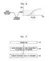
- FIG. 6is a diagram that schematically illustrates a method for adjusting read thresholds, in accordance with an alternative embodiment of the present invention.
- FIGS. 7-11are flow charts that schematically illustrate methods for adjusting read thresholds, in accordance with alternative embodiments of the present invention.
- FIG. 12is a graph showing threshold voltage distributions and read thresholds used in the method of FIG. 11 , in accordance with an embodiment of the present invention.
- the optimal values of the read thresholds used for retrieving data from analog memory cellsoften vary from one cell group to another, as well as over the lifetime of the memory. Accurate positioning of the read thresholds is crucial for maintaining low reading error probability, especially in high-density, multi-level cells.
- Embodiments of the present inventionprovide improved methods and systems for adaptively adjusting the read thresholds used for reading analog memory cells.
- a Memory Signal processorstores and retrieves data in an array of analog memory cells.
- the MSPestimates the Cumulative Distribution Function (CDF) of the storage values stored in the cells.
- the CDFis a function whose value, for any given storage value, is indicative of the number of cells (in absolute or relative terms) having storage values less than or equal to the given storage value.
- the MSPdetermines the optimal positions of the read thresholds based on the estimated CDF.
- the MSPadjusts the read thresholds to assume the optimal positions and reads data from the cells using the adjusted thresholds.
- threshold adaptation based on the CDFis superior to adaptation that is based on the storage value distributions themselves, since the CDF can typically be estimated by a much smaller number of data points in comparison with the Probability Distribution Function (PDF).
- PDFProbability Distribution Function
- the CDFis estimated based on the numbers of cells associated with the different programming levels.
- the MSPidentifies boundary regions that separate the different programming levels, and positions the read thresholds within the boundary regions.
- the MSPhas full or partial a-priori information regarding the distribution of storage values for a given programming level, and the MSP uses this information in computing the read thresholds.
- the MSPmaintains a model that produces a modeled CDF (also referred to as a target CDF) based on a number of input parameters.
- the MSPadapts the model parameters so as to fit the modeled CDF to the estimated (measured) CDF, and derives the read thresholds from the model.
- the modelcomprises a predefined set of target CDFs, and the MSP selects the target CDF that best fits the measured CDF.
- the MSPencodes the stored data using an Error Correction Code (ECC) and decodes the ECC when retrieving data.
- ECCError Correction Code
- the read thresholds used for reading a certain group of cellsare adjusted based on CDF measurements that were performed on the same group.
- CDF measurementsare performed on one group of cells, and are used to adjust the read thresholds of another group.
- the achieved reading performanceremains optimal over different cell groups, over the entire lifetime of the memory device, and in the presence of various types of distortion and interference.
- Analog memory cellsare programmed to store data by writing storage values (e.g., voltages or currents) to the cells.
- storage valuese.g., voltages or currents
- the target storage values that are used for programming the cellsare typically chosen from a finite set of nominal values that represent the data, the actual storage values stored in the cells may deviate from the nominal values. These deviations may be caused by several factors, such as inaccuracies in the programming process, drift due to device aging, cell wearing due to previous programming and erasure cycles, disturb noise caused by memory operations applied to other cells in the array and/or cross-coupling interference from other cells.
- the storage values of the cellstypically have a certain statistical distribution, which may vary from one cell group to another and/or over the lifetime of the memory cells.
- FIG. 1is a graph showing a distribution (upper plot) and a Cumulative Density Function (CDF, lower plot) of threshold voltages in a group of analog memory cells, in accordance with an embodiment of the present invention.
- the cellscomprise four-level cells, with each cell storing two data bits.
- Curves 20 A . . . 20 Dshow the distributions of threshold voltages in the group of cells. Each curve corresponds to a subset of the cells that are programmed to a certain programming level or state.
- Curves 20 A . . . 20 Dshow the threshold voltage distributions in the cells that are programmed with target storage values 22 A . . . 22 D, respectively.
- distribution 20 Acorresponds to an erased level.
- the storage values of the cellsare compared with read thresholds.
- three read thresholds TH 1 . . . TH 3are used to differentiate between the four levels.
- a curve 21shows the Cumulative Distribution Function (CDF) of the threshold voltages in the group of cells.
- CDFCumulative Distribution Function
- the same number of cellsis programmed to each of the four levels.
- the CDFreaches 1 ⁇ 4 between the first and second levels, 1 ⁇ 2 between the second and third levels, and 3 ⁇ 4 between the third and fourth levels.
- the slope of the CDFis steepest at the middle of distributions 20 A . . . 20 D, and is substantially flat at the boundary regions in between distributions 20 A . . . 20 D.
- FIG. 2is a block diagram that schematically illustrates a memory system 23 , in accordance with an embodiment of the present invention.
- System 23can be used in various host systems and devices, such as in computing devices, cellular phones or other communication terminals, removable memory modules (“disk-on-key” devices), digital cameras, music and other media players and/or any other system or device in which data is stored and retrieved.
- System 23comprises a memory device 24 , which stores data in a memory cell array 28 .
- the memory arraycomprises multiple analog memory cells 32 .
- analog memory cellis used to describe any memory cell that holds a continuous, analog value of a physical parameter, such as an electrical voltage or charge.
- Array 28may comprise analog memory cells of any kind, such as, for example, NAND, NOR and CTF Flash cells, PCM, NROM, FRAM, MRAM and DRAM cells.
- analog memory cellssuch as, for example, NAND, NOR and CTF Flash cells, PCM, NROM, FRAM, MRAM and DRAM cells.
- the charge levels stored in the cells and/or the analog voltages or currents written into and read out of the cellsare referred to herein collectively as analog values or storage values.
- System 23stores data in the analog memory cells by programming the cells to assume respective memory states.
- the memory statesare selected from a finite set of possible states, and each state corresponds to a certain nominal analog value. For example, a 2 bit/cell MLC can be programmed to assume one of four possible memory states by writing one of four possible nominal analog values into the cell.
- Data for storage in memory device 24is provided to the device and cached in data buffers 36 .
- the datais then converted to analog voltages and written into memory cells 32 using a reading/writing (R/W) unit 40 , whose functionality is described in greater detail below.
- R/W unit 40converts the electrical charge, and thus the analog voltages of memory cells 32 , into digital samples having a resolution of one or more bits.
- the samplesare cached in buffers 36 .
- the operation and timing of memory device 24is managed by control logic 48 .
- MSP 52comprises a signal processing unit 60 , which processes the data that is written into and read from device 24 .
- unit 60encodes the data to be written into the memory cells using an Error Correction Code (ECC), and decodes the ECC of the retrieved data.
- ECCError Correction Code
- Unit 60may use a Bose-Chaudhuri-Hocquenghem (BCH) code, a Low Density Parity Chack (LDPC) code, or any other suitable type of ECC known in the art.
- BCHBose-Chaudhuri-Hocquenghem
- LDPCLow Density Parity Chack
- MSP 52carries out methods for adaptively adjusting the positions of the read thresholds used for reading data from cells 32 , as will be described in detail below.
- MSP 52comprises a data buffer 72 , which is used by unit 60 for storing data and for interfacing with memory device 24 .
- MSP 52also comprises an Input/Output (I/O) buffer 56 , which forms an interface between the MSP and the host system.
- a controller 76manages the operation and timing of MSP 52 .
- Signal processing unit 60 and controller 76may be implemented in hardware. Alternatively, unit 60 and/or controller 76 may comprise microprocessors that run suitable software, or a combination of hardware and software elements.
- FIG. 2is an exemplary system configuration, which is shown purely for the sake of conceptual clarity. Any other suitable configuration can also be used. Elements that are not necessary for understanding the principles of the present invention, such as various interfaces, addressing circuits, timing and sequencing circuits and debugging circuits, have been omitted from the figure for clarity.
- memory device 24 and MSP 52are implemented as two separate Integrated Circuits (ICs). In alternative embodiments, however, the memory device and MSP may be integrated on separate semiconductor dies in a single Multi-Chip Package (MCP) or System on Chip (SoC). Further alternatively, some or all of the MSP circuitry may reside on the same die on which memory array 28 is disposed. Further alternatively, some or all of the functionality of MSP 52 can be implemented in software and carried out by a processor or other element of the host system. In some implementations, a single MSP 52 may be connected to multiple memory devices 24 .
- MCPMulti-Chip Package
- SoCSystem on Chip
- data to be written into memory device 24is accepted from the host and cached in I/O buffer 56 .
- the datais transferred, via data buffers 72 , to memory device 24 .
- the datamay be pre-processed by MSP 52 before it is transferred to the memory device for programming.
- unit 60may encode the data using an ECC, add certain data for internal use, and/or scramble the data.
- the datais temporarily stored in buffers 36 .
- R/W unit 40converts the data to nominal analog values and writes the nominal values into the appropriate cells 32 of array 28 .
- R/W unit 40reads analog values (storage values) out of the appropriate memory cells 32 and converts them to soft digital samples by comparing the read storage values to the read thresholds.
- the samplesare cached in buffers 36 and transferred to buffers 72 of MSP 52 .
- unit 60 of MSP 52converts the samples to data bits and provides the reconstructed data as output.
- FIG. 3is a diagram that schematically illustrates memory cell array 28 , in accordance with an embodiment of the present invention.
- FIG. 3refers to Flash memory cells that are connected in a particular array configuration, the principles of the present invention are applicable to other types of memory cells and other array configurations, as well.
- Some exemplary cell types and array configurationsare described in the references cited in the Background section above.
- Memory cells 32 of array 28are arranged in a grid having multiple rows and columns.
- Each cell 32comprises a floating gate Metal-Oxide Semiconductor (MOS) transistor.
- MOSMetal-Oxide Semiconductor
- a certain amount of electrical charge (electrons or holes)can be stored in a particular cell by applying appropriate voltage levels to the transistor gate, source and drain.
- the value stored in the cellcan be read by measuring the threshold voltage of the cell, which is defined as the minimal voltage that needs to be applied to the gate of the transistor in order to cause the transistor to conduct.
- the read threshold voltageis indicative of the charge stored in the cell.
- the gates of the transistors in each roware connected by word lines 80 .
- the sources of the transistors in each columnare connected by bit lines 84 .
- the sourcesare connected to the bit lines directly.
- the bit linesare connected to strings of floating-gate cells.
- the memory cell arrayis typically divided into multiple pages, i.e., groups of memory cells that are programmed and read simultaneously. Pages are sometimes sub-divided into sectors.
- each pagecomprises an entire row of the array.
- each row (word line)can be divided into two or more pages.
- each rowis divided into two pages, one comprising the odd-order cells and the other comprising the even-order cells.
- a two-bit-per-cell memory devicemay have four pages per row
- a three-bit-per-cell memory devicemay have six pages per row
- a four-bit-per-cell memory devicemay have eight pages per row.
- Erasing of cellsis usually carried out in blocks that contain multiple pages.
- Typical memory devicesmay comprise several thousand erasure blocks.
- each erasure blockis on the order of 32 word lines, each comprising several thousand cells.
- Each word line of such a deviceis often partitioned into four pages (odd/even order cells, least/most significant bit of the cells).
- Three-bit-per cell devices having 32 word lines per erasure blockwould have 192 pages per erasure block, and four-bit-per-cell devices would have 256 pages per block.
- other block sizes and configurationscan also be used.
- Some memory devicescomprise two or more separate memory cell arrays, often referred to as planes. Since each plane has a certain “busy” period between successive write operations, data can be written alternately to the different planes in order to increase programming speed.
- the positions of the read thresholds used for reading the memory cellshave a considerable effect on the reading quality, i.e., on the decoding error probability.
- the read thresholdsshould be positioned appropriately with respect to the threshold voltage distributions, so that the probability that a read storage value belonging to a certain level will fall on the wrong side of a read threshold is minimized.
- the threshold voltage distributions of the memory cellsvary over the lifetime of the memory cells, it is important to continually track these variations and adjust the threshold positions accordingly.
- Adaptive setting of read thresholdsis particularly important in cells having a large number of programming levels (e.g., eight-level or sixteen-level MLC). In such cells, the different levels are closely-packed on the voltage axis, and voltage distributions often overlap one another given a certain amount of aging and interference. Therefore, the decoding error probability in these cells is highly-sensitive to non-optimal threshold positions.
- the methods and systems described hereinestimate and adjust the positions of read thresholds, based on the Cumulative Distribution Function (CDF) of the storage values. Threshold estimation and adjustment can be performed at any time and at any frequency, such as in production, during the operational lifetime of the memory device, at periodic intervals, after power-up, as a background low-priority task that operates concurrently with memory access operations, after reading data, after writing data, in response to certain events or conditions, or in accordance with any other suitable logic.
- CDFCumulative Distribution Function
- FIG. 4is a flow chart that schematically illustrates a method for data storage and retrieval, in accordance with an embodiment of the present invention.
- the description that followsrefers to a single page of memory cells. However, the method is applicable to any other suitable group of cells.
- the methodcan also be used in an inter-page manner, by using measurements acquired in one page for adjusting the thresholds of another page, as described further below.
- the methodbegins with MSP 52 storing data in a page of memory cells 32 in array 28 by programming the cells with appropriate storage values, at a data storage step 90 .
- the MSPis requested to retrieve the data from the memory cells, such as in response to a host command.
- Data retrievalmay be requested at any time, e.g., seconds, hours, days or even years after the data was stored.
- the MSPadjusts the positions of the read thresholds that will be used to read the cells.
- the MSPreads the storage values (in the present example, the threshold voltages) from the memory cells, at a reading step 94 .
- the MSPreads the storage values from the entire page in a single read operation.
- the read operationcompares the storage values of the cells in the page to a certain read threshold, and produces indications (hard decisions) as to whether the storage values are smaller or greater than the read threshold.
- the MSPestimates the CDF of the threshold voltages of the page, at a CDF estimation step 98 .
- the MSPdetermines the number N of cells in the page whose threshold voltage is smaller than the threshold.
- the pair ⁇ N,V>forms a single datapoint on the CDF of the threshold voltages of the page.
- the MSPmay estimate the CDF at various accuracy or resolution levels, depending on the number of measured CDF datapoints. In other words, the MSP can improve the CDF estimation by performing a larger number of read operations with different thresholds, and vice versa.
- processing CDF functionsis more efficient in terms of memory usage than processing CDF ⁇ 1 functions.
- processing CDF ⁇ 1 functionsis often more efficient in terms of computational complexity.
- the MSPadjusts the positions of the read thresholds based on the estimated CDF, at a threshold adjustment step 102 .
- the MSPsets the read thresholds accordingly and retrieves the data using the adjusted thresholds, at a data retrieval step 106 .
- the MSPestimates the CDF over a subset of the storage values read from a given page, (e.g., over the values at the beginning of the page) in order to reduce reading time.
- multiple memory pagesare mapped to a single group of cells, such that each page is mapped to a certain bit.
- a certain pagemay be stored in the Least Significant Bits (LSB) of the cells, another page may be stored in the Central Significant Bits (CSB) of the cells and yet another page may be stored in the Most Significant Bits (MSB) of the cells.
- LSBLeast Significant Bits
- CSBCentral Significant Bits
- MSBMost Significant Bits
- eight programming levels L 1 . . . L 8are mapped to the data bit combinations “111”, “011”, “001”, “101”, “100”, “000”, “010”and “110”, in ascending order of storage values.
- This mappinghas a “gray coding” characteristic, in which adjacent programming levels differ from one another by only a single bit.
- the LSB in this casecan be read using a single read threshold located between levels L 4 and L 5 .
- the CSBcan be read using two read thresholds, located between levels L 2 and L 3 and between levels L 6 and L 7 .
- the MSBcan be read using four read thresholds, which are located between levels L 1 /L 2 , L 3 /L 4 , L 5 /L 6 and L 7 /L 8 .
- the MSPadjusts some or all of the read thresholds used for reading the data stored in the different MLC bits.
- the MSPmay obtain more than a single CDF data point in a given read operation.
- reading the LSB pageobtains one CDF data point
- reading the CSB pageobtains two additional data points
- reading the MSB pageobtains four additional data points.
- seven CDF data pointsare obtained in three read operations.
- FIGS. 5-11 belowshow several exemplary methods for adjusting the read thresholds based on the estimated CDF. Each method makes certain assumptions and has certain advantages and limitations, which are discussed below.
- the relative number of cells associated with each programming levelis known when the cells are to be read. For example, it can sometimes be assumed that each level has approximately the same number of cells. This condition holds, for example, when the data is scrambled. In other scenarios, the number of cells associated with each level is not the same, but the absolute numbers or ratios between them are known. For example, information indicative of the number of cells in the page that belong to each level can be stored in the page along with the data, or in another area of the memory.
- the MSPestimates the CDF based on the known number of cells associated with each level.
- the MSPmay then adjust the read thresholds based on the estimated CDF, using any of the techniques described herein.
- FIG. 5is a flow chart that schematically illustrates a method for estimating the CDF and adjusting the read thresholds, in accordance with an embodiment of the present invention.
- the methodassumes that the general shape of the storage value distribution (the PDF of the storage values) is known.
- the methodbegins with the MSP scaling the magnitude of the PDF of each programming level based on the relative number of cells associated with the level, at a scaling step 110 .
- the output of this stepis a set of PDFs, each having a relative magnitude that is proportional to the number of cells associated with the level.
- the number of cells in each individual levelis unknown, but the total number of cells in a certain group of levels is known. In such cases, the MSP may assume that the total known number of cells is distributed evenly among the levels in the group.
- the MSPintegrates the set of PDFs to produce an estimated CDF, at a CDF estimation step 114 .
- the MSPadjusts the read thresholds based on the estimated CDF, at a threshold adjustment step 118 .
- the MSPmay adjust the read thresholds using any of the techniques described herein.
- the MSPmay estimate the CDF based on the numbers of cells associated with a set of levels, without knowledge of the number of cells in each individual level. For example, when different pages are stored in different MLC bits, the MSP may record the number of “1” data bits in each page, without a need to combine data from different pages. The number associated with each page can be generated independently.
- This featuremay be used in the other CDF-based methods described herein. Assuming the cells are distributed evenly among programming levels (e.g., when the data is scrambled), the CDF can be estimated without explicit statistics related to individual pages. When the number of cells associated with each programming level (or group of levels) is known, the CDF estimation can be improved, as described above.
- the distribution of storage values in a given programming levelis known, but its absolute location on the storage value axis is not known.
- the storage value distribution of a particular levelis Gaussian and has a certain variance, but the mean of the distribution is unknown.
- Such a scenariooccurs, for example, when each level has a certain known distribution, which has an unknown drift due to aging.
- the absolute position of the storage value distributionshould be determined.
- FIG. 6is a diagram that schematically illustrates a method for adjusting read thresholds, in accordance with an alternative embodiment of the present invention.
- the method of FIG. 6assumes that the shape of the storage value distribution is known (and therefore the shape of the CDF is known, at least within a partial range of storage values), but its absolute position with respect to the thresholds is unknown.
- the MSPmeasures two CDF data points ( ⁇ N,V> pairs, as described above), at two values denoted TH A and TH B .
- ⁇ CDFCDF(TH B ) ⁇ CDF(TH A ).
- the value of ⁇ CDFuniquely determines the absolute position of the CDF on the storage value axis.
- the MSPdetermines the absolute position of the CDF (e.g., the mean of the storage value distribution) from the known CDF shape and the two CDF data points. The MSP then adjusts the read thresholds with respect to the known absolute position of the CDF.
- the absolute position of the CDFe.g., the mean of the storage value distribution
- all thresholdscan be set by performing 2n read operations, i.e., using 2n CDF data points.
- 2n read operationsi.e., using 2n CDF data points.
- a smaller number of CDF data pointsmay suffice.
- the MSPmay verify that the number of bits below TH 1 is 1/n of the total number, by performing 2n ⁇ 1 read operations.
- the MSPcan determine the absolute position of the storage value distribution using a single read operation, assuming the numbers of cells associated with the different levels are known.
- the MSPmay obtain a single CDF data point in the relevant region of a given programming level, and determine the absolute position of the level distribution based on the acquired data point and on the known relative number of cells associated with the respective programming level.
- the use of multiple CDF data pointsreduces the sensitivity of the estimation to the number of cells associated with each level, at the expense of additional read operations.
- the method abovecan also be used when the number of cells associated with each programming levels is not known. For example, when the data is scrambled, the MSP may assume that the cells are distributed evenly among the different programming levels.
- the storage value distributions of the different programming levelsare separated by well-defined boundary regions.
- the number of cells whose storage values fall in the boundary regionsis typically very small. Therefore, the CDF of the storage values is typically flat in these regions.
- the widths and absolute locations of the boundary regionsmay change over time, for example because of drift and widening of the storage value distributions.
- the MSPautomatically determines the locations of the boundary regions between programming levels, and positions the read thresholds within these regions.
- FIG. 7is a flow chart that schematically illustrates a method for adjusting read thresholds, in accordance with another embodiment of the present invention.
- the methodbegin with the MSP estimating the CDF of the storage values, at a CDF estimation step 124 , similarly to step 98 of FIG. 4 above.
- the MSPdetermines the boundary regions between adjacent programming levels by detecting flat regions in the estimated CDF, at a boundary detection step 128 . (In some cases, the CDF is not entirely flat in the boundary regions, but has a gentle slope. Thus, the term “flat region” also refers to a region whose slope is considerably gentler with respect to other regions.)
- the MSPpositions the read thresholds within the detected boundary regions, at a threshold positioning step 132 .
- the MSPpositions a single read threshold that differentiates between a pair of adjacent programming levels within the boundary region that separates the two levels.
- the MSPmay select the read threshold values from a set of predetermined threshold values, by selecting values that fall in relatively flat regions of the CDF.
- the MSPcan reduce the number of read operations performed in CDF estimation step 124 above. For example, for a given boundary region, the MSP can measure a single CDF data point that falls slightly above the boundary region, and derive the upper edge of the boundary region from the known CDF shape. The lower edge of the boundary region can be similarly determined using a single CDF data point falling slightly below the region. Thus, when the CDF shape is known, the MSP can determine the edge of a certain boundary region using only a single read operation (a single CDF data point).
- the MSPdefines and maintains a mathematical model that produces a target CDF based on one or more input parameters.
- the MSPcalculates the read thresholds by fitting the target CDF produced by the model to an estimated CDF derived from actual read operations.
- the MSPmay store a predefined set of target CDFs, and select the target CDF that best fits the estimated (measured) CDF.
- the set of target CDFsis also referred to herein as a model.
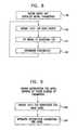
- FIG. 8is a flow chart that schematically illustrates a method for adjusting read thresholds, in accordance with an embodiment of the present invention.
- the method of FIG. 8is typically used when the properties of the CDF are not known a-priori.
- the methodbegins with the MSP defining a model that produces the target CDF and initializing the model parameters, at a model definition step 136 .
- the modelaccepts as input various parameters of the storage value distributions of the different levels.
- the input parametersmay comprise, for example, an offset (or an absolute position) and/or a scaling factor (shrinking/widening factor) for each of the programming levels.
- the input parametersmay be initially set to the best currently-known values or to any other suitable initial values.
- the modelcomprises a set of several CDFs (referred to as target CDFs), such as CDFs that are typical of various stages along the lifetime of the memory.
- target CDFssuch as CDFs that are typical of various stages along the lifetime of the memory.
- Such CDFsmay reflect, for example, different numbers of programming/erasure cycles that the cells have gone through, different degrees of cell aging or different temperature conditions.
- the target CDFsmay reflect different types of distortion that the cells may suffer from.
- Exemplary distortion estimation methodsare described, for example, in PCT Application WO 2007/132453, entitled “Distortion Estimation and Cancellation in Memory Devices,” filed May 10, 2007, and in PCT Application PCT/IL2007/001059, entitled “Estimation of Non-Linear Distortion in Memory Devices,” filed Aug. 27, 2007, whose disclosures are incorporated herein by reference.
- the MSPestimates the actual CDF of the storage values by measuring one or more CDF data points, at a CDF estimation step 140 .
- the MSPfits the model to the estimated (measured) CDF, at a fitting step 144 .
- the MSPattempts to estimate the input parameter values (e.g., the offsets and scaling factors of the different programming levels) for which the model produces a target CDF that best fits the estimated CDF.
- the MSPmay adjust the model based on the numbers of cells that are associated with different programming levels, as described above.
- the modelmay comprise an offset and a scaling factor for each of the seven non-erased levels, i.e., a total of fourteen parameters.
- a simpler modelmay use a smaller set of input parameters by assuming that all levels are subject to the same offset and/or the same scaling factor.
- any other suitable model having any suitable set of input parameterscan be used.
- a certain known dependencemay exist between the shifts and/or widening factors of the different levels (e.g., the shift of a certain level may be proportional to the central storage value of the level).
- the MSPmay use a smaller number of parameters and a smaller number of read operations.
- the modelcomprises a predefined set of target CDFs
- the MSPselects the target CDF that best fits the estimated CDF.
- the MSPmay fit the target CDF to the estimated CDF using a Maximum Likelihood (ML) criterion, as is known in the art, or using any other suitable fitting criterion or metric.
- MLMaximum Likelihood
- the MSPadjusts the read threshold values based on the fitting results, at a threshold adjustment step 148 .
- the modelmay produce read threshold values that match the target CDF.
- a corresponding set of optimal read thresholdsmay be stored with each target CDF.
- the MSPmay set the read thresholds based on the estimated CDF, using any of the techniques described herein. The method then loops back to step 140 above, and the MSP continues to estimate the actual storage value CDF and fit the model accordingly.
- the accuracy of the threshold adjustment process described abovedepends on the accuracy of the estimated CDF measured at step 140 , as well as on the accuracy of the model.
- the CDF estimation accuracygenerally depends on the number and quality of the measured CDF data points, which increases with the number of model fitting iterations. In some cases it is beneficial to obtain additional CDF data points before attempting to adapt the model. Therefore, the MSP may decide, at each iteration of the method of FIG. 8 , whether to try and fit the model parameters to the estimated CDF or to obtain additional CDF data points and improve the CDF estimation accuracy.
- the MSPmay carry out steps 140 and 144 concurrently.
- the MSPmay perform model fitting calculations on previously-obtained CDF data points, and in parallel obtain additional data points.
- FIG. 9is a flow chart that schematically illustrates another model-based method for adjusting read thresholds, in accordance with an alternative embodiment of the present invention.
- the method of FIG. 9assumes that the distribution of each programming level is known and is defined by a finite number of parameters. For example, in some cases it is known that the storage values in each level have a Gaussian distribution, which can be described using two parameters—the mean and the variance of the distribution.
- the methodbegins with the MSP measuring CDF data points separately for each programming level, at a level-specific measurement step 156 .
- the number of CDF data points measured per levelmatches the number of parameters used for representing the known distribution. For example, when each level has a Gaussian distribution, the MSP measures two CDF data points per level. The MSP then estimates the distribution parameters of each level, at a level-specific parameter estimation step 160 .
- the MSPcan adjust the read thresholds based on the known CDF, as described above.
- the number of measured CDF data pointscan be reduced when some of the distribution parameters are known, and/or when relationships between some of the distribution parameters can be assumed. For example, when the level distributions are Gaussian having known variances and only unknown offsets, the MSP can adjust the thresholds using only a single CDF data point per level. The number of data points can also be reduced, for example, when all levels can be assumed to have the same offset. Typically, the number of CDF data points can be reduced to the number of independent parameters.
- the MSPmay use different methods and criteria for determining which CDF data points to measure.
- a trade-offexists between measuring CDF data points located in the boundaries between programming levels and data points located inside the levels.
- CDF data points located within the programming levelsare often extremely valuable to the accuracy of the model, in comparison with data points that lie in boundary regions between programming levels.
- CDF data points located in the boundaries between levelscan be re-used for retrieving data from the cells, whereas data points in the middle of the programming levels can typically be used only for model fitting.
- the MSPmay measure CDF data points in the boundary regions, within the level distributions, or it may measure a combination of both types of data points.
- the actual CDFis known a-priori, with the exception of an unknown shift.
- Such a scenariooccurs, for example, as a result of temperature variations or when aging effects cause similar shifts in all levels.
- FIG. 10is a flow chart that schematically illustrates a method for adjusting read thresholds, in accordance with another embodiment of the present invention.
- the method of FIG. 10assumes that the CDF is known except for an unknown shift.
- the methodcan also be used when other unknown factors exist, but the shift is dominant. For example, when the CDF is subject to both shift and scaling, scaling may sometimes be neglected for small shift values.
- the methodbegins with the MSP measuring one or more CDF data points, at a CDF measurement step 168 .
- the MSPestimates the shift of the actual CDF from the measured data points, at a shift estimation step 172 .
- the MSPmay compare the measured CDF data points to a reference version of the known CDF and derive the shift value from the comparison.
- the MSPmay determine a reference voltage V REF in the reference CDF that would produce the same value of N.
- the offsetcan be estimated as V-V REF .
- the MSPmay average the calculated shift over a number of CDF data points.
- the MSPadjusts the read thresholds based on the estimated shift, at a threshold adjustment step 176 .
- the MSPcan calculate the adjusted thresholds by subtracting the estimated shift from each of the reference thresholds.
- the method of FIG. 10assumes that the relative number of cells associated with each level is similar in the measured CDF and in the reference CDF. In practice, however, this condition may not always hold. Deviations from this condition may introduce inaccuracies into the shift estimation, and therefore into the read threshold positions.
- the deviationcan be corrected, for example, by storing the number of cells whose values are smaller than a given threshold when the cells are programmed. This stored number is denoted N REC .
- N RECthe number of cells whose values are smaller than a given threshold when the cells are programmed.
- the measured CDF data point ⁇ N,V>is typically chosen close to the data point in the reference CDF.
- the CDF correction technique abovecan also be used in any of the other CDF estimation methods described herein.
- the MSPmay use any other suitable technique for correcting errors caused by deviations in the number of cells associated with each programming level.
- N RECmay be calculated over only a subset of the cells.
- correcting a certain read threshold using the method aboveinvolves the use of the N REC values of all levels that are below the threshold in question.
- correcting threshold TH 3uses the N REC values of the first three levels.
- the N REC valuesmay refer to numbers of cells that are associated with different memory pages, as described above.
- the model-based methods described abovemay define the model based on a certain distribution of data values.
- the group of memory cells over which the CDF is estimatedmay have a different distribution of data values.
- the group of memory cells for which the thresholds are adjustedmay be different from the group of memory cells over which the CDF was estimated, and may have yet another distribution of data values.
- the MSPcan correct the deviations caused by the different data value distributions using information regarding the actual distributions.
- the MSPcan estimate each read threshold separately, and at each stage process a single threshold.
- the MSPmay use standard read commands that are commonly used in such memory devices. Many devices, for example, read a given CSB page with two thresholds in a single command. In such a case, the MSP may calculate a differential CDF, i.e., the number of cells whose storage values fall between the two read thresholds. If all levels were subjected to similar shifts, the differential CDF will not change substantially. If, however, different levels have different shifts, the differential CDF can be used to estimate the relative shift of one threshold with respect to the other.
- a differential CDFi.e., the number of cells whose storage values fall between the two read thresholds. If all levels were subjected to similar shifts, the differential CDF will not change substantially. If, however, different levels have different shifts, the differential CDF can be used to estimate the relative shift of one threshold with respect to the other.
- the MSPcan estimate the absolute shift of other thresholds. Using this technique, the CDF estimation accuracy can be improved without a need to store the number of “1” bits in individual levels.
- the MSPencodes the data using an Error Correction Code (ECC) before storing the data in the memory cells.
- ECCError Correction Code
- the MSPdecodes the ECC in order to correct reading errors.
- a reading erroroccurs when the storage value of a certain cell falls on the wrong side of a threshold, e.g., in a storage value interval that corresponds to an adjacent programming level.
- the MSPcan determine the direction of the error, i.e., the programming level with which the read storage value was erroneously associated before applying ECC correction.
- the MSPcan use information regarding directions of corrected errors for adjusting the read thresholds.
- a read thresholdthat differentiates between two adjacent programming levels denoted L 1 and L 2 .
- the number of errors in both directions around this thresholdi.e., the number of read values that fell in level L 1 even though the cell was programmed to level L 2 , and the number of read values that fell in level L 2 even though the cell was programmed to level L 1
- An asymmetry in the number of corrected errors of opposite directionsmay indicate a non-optimal threshold position. For example, if the number of read values that fell in level L 1 even though the cell was programmed to level L 2 is considerably greater than the number of errors in the opposite direction, the threshold should most likely be moved toward level L 1 .
- FIG. 11is a flow chart that schematically illustrates a method for adjusting read thresholds, in accordance with an embodiment of the present invention.
- the methodbegins with the MSP retrieving ECC-encoded data from the cells and decoding the ECC, at a decoding step 180 .
- the MSPclassifies the errors corrected by the ECC into the different directions, at an error classification step 184 .
- the MSPcounts the number of errors in each class. For example, for a pair of levels denoted L 1 and L 2 , the MSP counts the number of corrected errors directed from L 1 to L 2 , and the number of corrected errors directed from L 2 to L 1 .
- the errors directed from L 1 to L 2comprise the errors in which the ECC corrected a “0” into a “1”
- the errors directed from L 2 to L 1comprise the errors in which the ECC corrected a “1” into a “0”.
- the MSPIn MLC devices in which different pages are mapped to different MLC bits using Gray-coded mapping, the MSP typically uses the data read from lower-order pages in order to identify the errors in a given page. The MSP uses the data read from lower-order pages to identify the errors that correspond to a given pair of levels, and/or to determine the read threshold that should be adjusted based on such errors. Alternatively, the MSP may assume that all thresholds are subject to the same amount of shift.
- the MSPadjusts the read thresholds based on the numbers of corrected errors of the different directions, at a threshold adjustment step 188 .
- the distribution (or CDF) of each levelis known, and the MSP takes the known distributions into account when calculating the threshold adjustment.
- FIG. 12is a graph showing threshold voltage distributions and read thresholds used in the method of FIG. 11 , in accordance with an embodiment of the present invention.
- plots 190 A and 190 Bshow the storage value distributions of programming levels L 1 and L 2 , respectively.
- the two distributionsare assumed to be Gaussian having known means (denoted ⁇ 1 and ⁇ 2 ) and variances (denoted ⁇ 1 and ⁇ 2 ).
- a current read threshold 194differentiates between the two levels.
- the number of corrected errors directed from level L 1 to level L 2is indicated by a region 198 A.
- the number of corrected errors directed in the opposite direction, from level L 2 to level L 1is indicated by a region 198 B.
- the area of region 198 Bis considerably larger than the area of region 198 A. Therefore, threshold 194 should be moved toward level L 1 .
- a Corrected read threshold 200is positioned at the optimal value, which balances the numbers of corrected errors in both directions.
- ⁇ 1 and ⁇ 2can be estimated as
- ⁇ ⁇ 1t - ⁇ 1 ⁇ Q - 1 ⁇ ( “ 1 ” ⁇ “ 0 ” total ⁇ ⁇ “ 1 ” )
- ⁇ ⁇ 2t - ⁇ 2 ⁇ Q - 1 ⁇ ( “ 0 ” ⁇ “ 1 ” total ⁇ ⁇ “ 0 ” )
- tdenotes the value of threshold 194
- “1” ⁇ “0”denotes the number of bits that the ECC decoder changed from “1” to “0”
- “0” ⁇ “1”denotes the number of bits that decoder changed from “0” to “1”
- total “1”denotes the total number of “1” bits after ECC correction
- total “0”denotes the total number of “0” bits after ECC correction.
- c⁇ 2 2 ⁇ ⁇ 1 2 - ⁇ 1 2 ⁇ ⁇ 2 2 - 2 ⁇ ⁇ 1 2 ⁇ ⁇ 2 2 ⁇ log ⁇ ( ⁇ 2 ⁇ 1 )
- x 1 , 2( ⁇ 2 2 ⁇ ⁇ 1 - ⁇ 1 2 ⁇ ⁇ 2 ) ⁇ ⁇ 1 ⁇ ⁇ 2 ⁇ ( ⁇ 1 - ⁇ 2 ) 2 - 2 ⁇ ( ⁇ 2 2 - ⁇ 1 2 ) ⁇ log ⁇ ( ⁇ 2 ⁇ 1 ) ( ⁇ 2 2 - ⁇ 1 2 )
- the midpoint between the two means ⁇ 1 and ⁇ 2can be used as a reference point.
- the shift of the optimal threshold with respect to the midpointcan be calculated by
- the latter methodcan also be used with non-Gaussian distributions.
- FIGS. 11 and 12addresses two programming levels.
- the MSPmay examine a specific page, and determine the appropriate programming levels using the data read from the other pages mapped to the same group of memory cells.
- the programming levels applicable to the CSB pagecan be determined based on the data read from the LSB page.
- the programming levels applicable to the MSB pagecan be determined based on the data read from the LSB and CSB pages.
- the LSB pagecan be processed independently of the other pages.
- the number of corrected errors directed from level L 1 to level L 2may differ from the number of errors in the opposite direction, even when the read threshold is set to the optimal position.
- the formulas given abovehandle this situation and nevertheless provide the optimal threshold position.
- the different threshold estimation methods described hereincan be used with different levels of a-priori uncertainty as to the optimal threshold locations. These scenarios can be roughly classified as threshold acquisition and threshold tracking scenarios.
- threshold acquisitionthe currently-used read thresholds are very far from optimal. Acquisition scenarios occur, for example, after power-up or following a long period in which the thresholds were not adapted.
- threshold trackingthe thresholds that are currently in use have relatively small deviations from the optimal positions. Tracking scenarios occur, for example, when the MSP continually estimates and adjusts the threshold positions to track gradual changes in the memory device.
- FIGS. 8-10are particularly suitable for threshold acquisition, although they can also be used for tracking.
- the methods of FIGS. 11 and 12are particularly suitable for threshold tracking, although they can also be used for threshold acquisition.
- the techniques that are based on ECC assistance and on counting the number of “1” or “0” bitsare best suited for threshold tracking.
- the threshold estimation methods described hereinare used for adjusting the read thresholds within a certain page.
- the measurements and computationsare performed over the memory cells of a certain page, and the results are used for adjusting the thresholds of the same page.
- Such a configurationis referred to as intra-page threshold estimation.
- the measurements and computationsare performed over a certain page, and the results are used to adjust the thresholds of a different page.
- Such a configurationis referred to as inter-page threshold estimation. (Although the description that follows refers to memory pages, the methods described herein are similarly applicable to any other suitable groups of memory cells.)
- the source pagei.e., the page over which the measurements are performed
- the target pagethe page whose thresholds are modified
- the MSPadapts the threshold adjustment to the specific characteristics of the target page. For example, for each page and for a given read threshold value, the MSP may store the number of cells in the page whose storage values are below the threshold. The MSP can then correct the threshold adjustment using this characteristic of the target page. A similar correction can be applied in intra-page operation, as well.
- Each cellstores three data bits denoted LSB, CSB and USB in a Gray-coded mapping.
- the cell LSBsstore a certain page
- the USBsstore another page
- the MSBsstore a third page.
- the LSB and USB pagesare already retrieved and their read thresholds are set.
- the MSPhas three threshold offsets—one for the LSB and two for the USB. The MSP can use the three offsets for calculating the read threshold adjustment of the MSB page.
- threshold adjustment informationcan be used between different word lines, different erasure blocks, different planes, different dies originating from a certain wafer, and/or between any other suitable groups of cells.
- the threshold correctionmay vary from one word line to the next in accordance with a certain dependence that can be estimated and tracked.
- the threshold correction in odd and even pages in a certain word linemay be correlative.
- certain word lines within a blockmay exhibit different threshold behavior. For example, in a 32-line erasure block, word lines 0 to 4 may exhibit large threshold variation between word lines, word lines 5 - 25 may exhibit little or no variation, and word lines 26 - 31 may again exhibit large variations.
- the MSPcan take these characteristics into account by restricting the allowed variations between word lines 5 - 25 , and allowing large changes between the other word lines.
- the MSPmay record and use information regarding errors that were corrected by the ECC in each page in order to correct the read threshold adjustment between pages. Further additionally or alternatively, the MSP may correct the thresholds between different pages based on the number of “1” bits and/or the “0” bits in the page. (When Gray mapping is used, the number of “1” bits in a page equals the number of cells that is associated with a set of programming levels.) These counts can be stored, for example, when the page is programmed.
- HDDHard Disk Drives
- the embodiments described hereinmainly refer to estimation and adaptation of read thresholds, the methods described herein can be similarly be used to compute other types of thresholds used for processing the storage values in analog memory cells, such as programming thresholds and verification thresholds.
- the MSPreads a given group of memory cells (e.g., a page) using multiple read thresholds.
- the datais encoded with an ECC before it is stored in the memory cells.
- the MSPcomputes soft decoding metrics based on the multiple read results, and decodes the ECC using the metrics.
- the threshold estimation and adjustment methods described hereincan be used to determine the values of the multiple read thresholds used for producing the soft decoding metrics. Using the methods and systems described herein, the number of read operations performed on each group of memory cells can be reduced.
- the MSPestimates and cancels distortion that is present in the storage values read from the memory cells.
- the MSPmay position the read thresholds used for reading the cells using the methods and systems described herein, so as to reduce the number of read operations.
Landscapes
- Engineering & Computer Science (AREA)
- Microelectronics & Electronic Packaging (AREA)
- Computer Security & Cryptography (AREA)
- Computer Hardware Design (AREA)
- Read Only Memory (AREA)
- Radar Systems Or Details Thereof (AREA)
Abstract
Description
wherein t denotes the value of
Claims (47)
Priority Applications (1)
| Application Number | Priority Date | Filing Date | Title |
|---|---|---|---|
| US12/522,175US8369141B2 (en) | 2007-03-12 | 2008-03-11 | Adaptive estimation of memory cell read thresholds |
Applications Claiming Priority (5)
| Application Number | Priority Date | Filing Date | Title |
|---|---|---|---|
| US89429007P | 2007-03-12 | 2007-03-12 | |
| US1682407P | 2007-12-27 | 2007-12-27 | |
| US1717707P | 2007-12-28 | 2007-12-28 | |
| PCT/IL2008/000329WO2008111058A2 (en) | 2007-03-12 | 2008-03-11 | Adaptive estimation of memory cell read thresholds |
| US12/522,175US8369141B2 (en) | 2007-03-12 | 2008-03-11 | Adaptive estimation of memory cell read thresholds |
Related Parent Applications (1)
| Application Number | Title | Priority Date | Filing Date |
|---|---|---|---|
| PCT/IL2008/000329A-371-Of-InternationalWO2008111058A2 (en) | 2007-03-12 | 2008-03-11 | Adaptive estimation of memory cell read thresholds |
Related Child Applications (1)
| Application Number | Title | Priority Date | Filing Date |
|---|---|---|---|
| US13/734,335ContinuationUS8547740B2 (en) | 2007-03-12 | 2013-01-04 | Adaptive estimation of memory cell read thresholds |
Publications (2)
| Publication Number | Publication Date |
|---|---|
| US20100091535A1 US20100091535A1 (en) | 2010-04-15 |
| US8369141B2true US8369141B2 (en) | 2013-02-05 |
Family
ID=39760192
Family Applications (2)
| Application Number | Title | Priority Date | Filing Date |
|---|---|---|---|
| US12/522,175Expired - Fee RelatedUS8369141B2 (en) | 2007-03-12 | 2008-03-11 | Adaptive estimation of memory cell read thresholds |
| US13/734,335ActiveUS8547740B2 (en) | 2007-03-12 | 2013-01-04 | Adaptive estimation of memory cell read thresholds |
Family Applications After (1)
| Application Number | Title | Priority Date | Filing Date |
|---|---|---|---|
| US13/734,335ActiveUS8547740B2 (en) | 2007-03-12 | 2013-01-04 | Adaptive estimation of memory cell read thresholds |
Country Status (3)
| Country | Link |
|---|---|
| US (2) | US8369141B2 (en) |
| CN (1) | CN101715595A (en) |
| WO (1) | WO2008111058A2 (en) |
Cited By (63)
| Publication number | Priority date | Publication date | Assignee | Title |
|---|---|---|---|---|
| US20110035540A1 (en)* | 2009-08-10 | 2011-02-10 | Adtron, Inc. | Flash blade system architecture and method |
| US20130010540A1 (en)* | 2010-04-20 | 2013-01-10 | Micron Technology, Inc. | Programming methods for a memory device |
| US20130073822A1 (en)* | 2011-09-20 | 2013-03-21 | Eran Sandel | Adaptive mapping of logical addresses to memory devices in solid state drives |
| US20130121080A1 (en)* | 2007-03-12 | 2013-05-16 | Apple Inc. | Adaptive Estimation of Memory Cell Read Thresholds |
| US20130166815A1 (en)* | 2008-06-11 | 2013-06-27 | Micron Technology, Inc. | Memory controllers to output data signals of a number of bits and to receive data signals of a different number of bits |
| US8693257B2 (en) | 2011-10-18 | 2014-04-08 | Seagate Technology Llc | Determining optimal read reference and programming voltages for non-volatile memory using mutual information |
| US8711619B2 (en) | 2011-10-18 | 2014-04-29 | Seagate Technology Llc | Categorizing bit errors of solid-state, non-volatile memory |
| US8760932B2 (en) | 2011-10-18 | 2014-06-24 | Seagate Technology Llc | Determination of memory read reference and programming voltages |
| US8909851B2 (en) | 2011-02-08 | 2014-12-09 | SMART Storage Systems, Inc. | Storage control system with change logging mechanism and method of operation thereof |
| US8935466B2 (en) | 2011-03-28 | 2015-01-13 | SMART Storage Systems, Inc. | Data storage system with non-volatile memory and method of operation thereof |
| US8949689B2 (en) | 2012-06-11 | 2015-02-03 | SMART Storage Systems, Inc. | Storage control system with data management mechanism and method of operation thereof |
| US20150052387A1 (en)* | 2013-08-14 | 2015-02-19 | Infineon Technologies Ag | Systems and methods utilizing a flexible read reference for a dynamic read window |
| WO2015023259A1 (en)* | 2013-08-13 | 2015-02-19 | Empire Technology Development Llc. | Memory systems |
| US9021231B2 (en) | 2011-09-02 | 2015-04-28 | SMART Storage Systems, Inc. | Storage control system with write amplification control mechanism and method of operation thereof |
| US9021319B2 (en) | 2011-09-02 | 2015-04-28 | SMART Storage Systems, Inc. | Non-volatile memory management system with load leveling and method of operation thereof |
| US9043780B2 (en) | 2013-03-27 | 2015-05-26 | SMART Storage Systems, Inc. | Electronic system with system modification control mechanism and method of operation thereof |
| US9063844B2 (en) | 2011-09-02 | 2015-06-23 | SMART Storage Systems, Inc. | Non-volatile memory management system with time measure mechanism and method of operation thereof |
| US9098399B2 (en) | 2011-08-31 | 2015-08-04 | SMART Storage Systems, Inc. | Electronic system with storage management mechanism and method of operation thereof |
| US9123445B2 (en) | 2013-01-22 | 2015-09-01 | SMART Storage Systems, Inc. | Storage control system with data management mechanism and method of operation thereof |
| US9135109B2 (en) | 2013-03-11 | 2015-09-15 | Seagate Technology Llc | Determination of optimum threshold voltage to read data values in memory cells |
| US9146850B2 (en) | 2013-08-01 | 2015-09-29 | SMART Storage Systems, Inc. | Data storage system with dynamic read threshold mechanism and method of operation thereof |
| US9152555B2 (en) | 2013-11-15 | 2015-10-06 | Sandisk Enterprise IP LLC. | Data management with modular erase in a data storage system |
| US9170941B2 (en) | 2013-04-05 | 2015-10-27 | Sandisk Enterprises IP LLC | Data hardening in a storage system |
| US9183137B2 (en) | 2013-02-27 | 2015-11-10 | SMART Storage Systems, Inc. | Storage control system with data management mechanism and method of operation thereof |
| US9214965B2 (en) | 2013-02-20 | 2015-12-15 | Sandisk Enterprise Ip Llc | Method and system for improving data integrity in non-volatile storage |
| US9239781B2 (en) | 2012-02-07 | 2016-01-19 | SMART Storage Systems, Inc. | Storage control system with erase block mechanism and method of operation thereof |
| US9244519B1 (en) | 2013-06-25 | 2016-01-26 | Smart Storage Systems. Inc. | Storage system with data transfer rate adjustment for power throttling |
| US9298252B2 (en) | 2012-04-17 | 2016-03-29 | SMART Storage Systems, Inc. | Storage control system with power down mechanism and method of operation thereof |
| US9313874B2 (en) | 2013-06-19 | 2016-04-12 | SMART Storage Systems, Inc. | Electronic system with heat extraction and method of manufacture thereof |
| US9319073B2 (en) | 2014-02-11 | 2016-04-19 | Seagate Technology Llc | Mitigation of write errors in multi-level cell flash memory through adaptive error correction code decoding |
| US9329928B2 (en) | 2013-02-20 | 2016-05-03 | Sandisk Enterprise IP LLC. | Bandwidth optimization in a non-volatile memory system |
| US9361222B2 (en) | 2013-08-07 | 2016-06-07 | SMART Storage Systems, Inc. | Electronic system with storage drive life estimation mechanism and method of operation thereof |
| US9367353B1 (en) | 2013-06-25 | 2016-06-14 | Sandisk Technologies Inc. | Storage control system with power throttling mechanism and method of operation thereof |
| US9390794B2 (en) | 2014-05-21 | 2016-07-12 | SK Hynix Inc. | Semiconductor device and operating method thereof |
| US9431113B2 (en) | 2013-08-07 | 2016-08-30 | Sandisk Technologies Llc | Data storage system with dynamic erase block grouping mechanism and method of operation thereof |
| US9448946B2 (en) | 2013-08-07 | 2016-09-20 | Sandisk Technologies Llc | Data storage system with stale data mechanism and method of operation thereof |
| US9470720B2 (en) | 2013-03-08 | 2016-10-18 | Sandisk Technologies Llc | Test system with localized heating and method of manufacture thereof |
| US9477540B2 (en) | 2013-11-28 | 2016-10-25 | Globalfoundries Inc. | Multi-stage codeword detector |
| US9543025B2 (en) | 2013-04-11 | 2017-01-10 | Sandisk Technologies Llc | Storage control system with power-off time estimation mechanism and method of operation thereof |
| US9645763B2 (en) | 2014-01-13 | 2017-05-09 | Seagate Technology Llc | Framework for balancing robustness and latency during collection of statistics from soft reads |
| US9671962B2 (en) | 2012-11-30 | 2017-06-06 | Sandisk Technologies Llc | Storage control system with data management mechanism of parity and method of operation thereof |
| US9697075B2 (en) | 2015-09-08 | 2017-07-04 | Apple Inc. | Efficient search for optimal read thresholds in flash memory |
| US9779818B2 (en) | 2015-07-09 | 2017-10-03 | Apple Inc. | Adaptation of high-order read thresholds |
| US9898056B2 (en) | 2013-06-19 | 2018-02-20 | Sandisk Technologies Llc | Electronic assembly with thermal channel and method of manufacture thereof |
| US10008277B2 (en) | 2016-09-12 | 2018-06-26 | Sandisk Technologies Llc | Block health monitoring using threshold voltage of dummy memory cells |
| US10049037B2 (en) | 2013-04-05 | 2018-08-14 | Sandisk Enterprise Ip Llc | Data management in a storage system |
| US10062433B2 (en) | 2015-02-23 | 2018-08-28 | Micron Technology, Inc. | Apparatuses and methods of reading memory cells |
| US10229749B2 (en) | 2017-03-31 | 2019-03-12 | Samsung Electronics Co., Ltd. | Nonvolatile memory storage system |
| US10381090B2 (en) | 2017-03-31 | 2019-08-13 | Samsung Electronics Co., Ltd. | Operation method of nonvolatile memory device and storage device |
| US10388394B2 (en) | 2017-07-25 | 2019-08-20 | Apple Inc. | Syndrome weight based evaluation of memory cells performance using multiple sense operations |
| US10546648B2 (en) | 2013-04-12 | 2020-01-28 | Sandisk Technologies Llc | Storage control system with data management mechanism and method of operation thereof |
| US10838810B2 (en)* | 2013-05-22 | 2020-11-17 | Seagate Technology Llc | Systems and methods for inter-cell interference mitigation in a flash memory |
| US11355204B2 (en) | 2020-09-03 | 2022-06-07 | SK Hynix Inc. | Efficient read-threshold calculation method for parametric PV-level modeling |
| US11430530B2 (en) | 2021-01-25 | 2022-08-30 | SK Hynix Inc. | Deep learning based program-verify modeling and voltage estimation for memory devices |
| US11514999B2 (en) | 2021-04-16 | 2022-11-29 | SK Hynix Inc. | Systems and methods for parametric PV-level modeling and read threshold voltage estimation |
| US11537842B2 (en) | 2018-11-14 | 2022-12-27 | Samsung Electronics Co., Ltd. | Storage device inferring read levels based on artificial neural network model and learning method of artificial neural network model |
| US11749354B2 (en) | 2021-07-13 | 2023-09-05 | SK Hynix Inc. | Systems and methods for non-parametric PV-level modeling and read threshold voltage estimation |
| US11769555B2 (en) | 2021-07-27 | 2023-09-26 | SK Hynix Inc. | Read threshold voltage estimation systems and methods for parametric PV-level modeling |
| US11769556B2 (en) | 2021-07-27 | 2023-09-26 | SK Hynix Inc. | Systems and methods for modeless read threshold voltage estimation |
| US11854629B2 (en) | 2021-11-22 | 2023-12-26 | SK Hynix Inc. | System and method for non-parametric optimal read threshold estimation using deep neural network |
| US11907571B2 (en) | 2020-07-13 | 2024-02-20 | SK Hynix Inc. | Read threshold optimization systems and methods using domain transformation |
| US12148496B2 (en) | 2022-06-29 | 2024-11-19 | Apple Inc. | Readout from memory cells subjected to perturbations in threshold voltage distributions |
| US12183410B2 (en) | 2020-10-14 | 2024-12-31 | Ams International Ag | Data storage apparatus comprising cell section operable as dosimeter and method of operating |
Families Citing this family (276)
| Publication number | Priority date | Publication date | Assignee | Title |
|---|---|---|---|---|
| KR101202537B1 (en) | 2006-05-12 | 2012-11-19 | 애플 인크. | Combined distortion estimation and error correction coding for memory devices |
| WO2007132456A2 (en) | 2006-05-12 | 2007-11-22 | Anobit Technologies Ltd. | Memory device with adaptive capacity |
| WO2007132452A2 (en) | 2006-05-12 | 2007-11-22 | Anobit Technologies | Reducing programming error in memory devices |
| WO2007132453A2 (en) | 2006-05-12 | 2007-11-22 | Anobit Technologies Ltd. | Distortion estimation and cancellation in memory devices |
| WO2008026203A2 (en) | 2006-08-27 | 2008-03-06 | Anobit Technologies | Estimation of non-linear distortion in memory devices |
| US7975192B2 (en) | 2006-10-30 | 2011-07-05 | Anobit Technologies Ltd. | Reading memory cells using multiple thresholds |
| WO2008053473A2 (en) | 2006-10-30 | 2008-05-08 | Anobit Technologies Ltd. | Memory cell readout using successive approximation |
| US7924648B2 (en) | 2006-11-28 | 2011-04-12 | Anobit Technologies Ltd. | Memory power and performance management |
| US7706182B2 (en) | 2006-12-03 | 2010-04-27 | Anobit Technologies Ltd. | Adaptive programming of analog memory cells using statistical characteristics |
| WO2008068747A2 (en) | 2006-12-03 | 2008-06-12 | Anobit Technologies Ltd. | Automatic defect management in memory devices |
| US8019938B2 (en) | 2006-12-06 | 2011-09-13 | Fusion-I0, Inc. | Apparatus, system, and method for solid-state storage as cache for high-capacity, non-volatile storage |
| US9495241B2 (en) | 2006-12-06 | 2016-11-15 | Longitude Enterprise Flash S.A.R.L. | Systems and methods for adaptive data storage |
| US9116823B2 (en) | 2006-12-06 | 2015-08-25 | Intelligent Intellectual Property Holdings 2 Llc | Systems and methods for adaptive error-correction coding |
| US8489817B2 (en) | 2007-12-06 | 2013-07-16 | Fusion-Io, Inc. | Apparatus, system, and method for caching data |
| US7900102B2 (en) | 2006-12-17 | 2011-03-01 | Anobit Technologies Ltd. | High-speed programming of memory devices |
| US7593263B2 (en) | 2006-12-17 | 2009-09-22 | Anobit Technologies Ltd. | Memory device with reduced reading latency |
| US8151166B2 (en) | 2007-01-24 | 2012-04-03 | Anobit Technologies Ltd. | Reduction of back pattern dependency effects in memory devices |
| US7751240B2 (en) | 2007-01-24 | 2010-07-06 | Anobit Technologies Ltd. | Memory device with negative thresholds |
| US8001320B2 (en) | 2007-04-22 | 2011-08-16 | Anobit Technologies Ltd. | Command interface for memory devices |
| US7903468B2 (en) | 2007-04-23 | 2011-03-08 | Ramot At Telaviv University Ltd. | Adaptive dynamic reading of flash memories |
| US8234545B2 (en) | 2007-05-12 | 2012-07-31 | Apple Inc. | Data storage with incremental redundancy |
| WO2008139441A2 (en) | 2007-05-12 | 2008-11-20 | Anobit Technologies Ltd. | Memory device with internal signal processing unit |
| US7925936B1 (en) | 2007-07-13 | 2011-04-12 | Anobit Technologies Ltd. | Memory device with non-uniform programming levels |
| US8174905B2 (en) | 2007-09-19 | 2012-05-08 | Anobit Technologies Ltd. | Programming orders for reducing distortion in arrays of multi-level analog memory cells |
| US8365040B2 (en) | 2007-09-20 | 2013-01-29 | Densbits Technologies Ltd. | Systems and methods for handling immediate data errors in flash memory |
| US8650352B2 (en)* | 2007-09-20 | 2014-02-11 | Densbits Technologies Ltd. | Systems and methods for determining logical values of coupled flash memory cells |
| US7773413B2 (en) | 2007-10-08 | 2010-08-10 | Anobit Technologies Ltd. | Reliable data storage in analog memory cells in the presence of temperature variations |
| US8527819B2 (en) | 2007-10-19 | 2013-09-03 | Apple Inc. | Data storage in analog memory cell arrays having erase failures |
| US8068360B2 (en) | 2007-10-19 | 2011-11-29 | Anobit Technologies Ltd. | Reading analog memory cells using built-in multi-threshold commands |
| US8000141B1 (en) | 2007-10-19 | 2011-08-16 | Anobit Technologies Ltd. | Compensation for voltage drifts in analog memory cells |
| US8694715B2 (en) | 2007-10-22 | 2014-04-08 | Densbits Technologies Ltd. | Methods for adaptively programming flash memory devices and flash memory systems incorporating same |
| US8427867B2 (en)* | 2007-10-22 | 2013-04-23 | Densbits Technologies Ltd. | Systems and methods for averaging error rates in non-volatile devices and storage systems |
| US8443242B2 (en)* | 2007-10-25 | 2013-05-14 | Densbits Technologies Ltd. | Systems and methods for multiple coding rates in flash devices |
| US8270246B2 (en) | 2007-11-13 | 2012-09-18 | Apple Inc. | Optimized selection of memory chips in multi-chips memory devices |
| US8225181B2 (en) | 2007-11-30 | 2012-07-17 | Apple Inc. | Efficient re-read operations from memory devices |
| US8321625B2 (en) | 2007-12-05 | 2012-11-27 | Densbits Technologies Ltd. | Flash memory device with physical cell value deterioration accommodation and methods useful in conjunction therewith |
| US8335977B2 (en)* | 2007-12-05 | 2012-12-18 | Densbits Technologies Ltd. | Flash memory apparatus and methods using a plurality of decoding stages including optional use of concatenated BCH codes and/or designation of “first below” cells |
| WO2009072105A2 (en)* | 2007-12-05 | 2009-06-11 | Densbits Technologies Ltd. | A low power chien-search based bch/rs decoding system for flash memory, mobile communications devices and other applications |
| US8316277B2 (en) | 2007-12-06 | 2012-11-20 | Fusion-Io, Inc. | Apparatus, system, and method for ensuring data validity in a data storage process |
| US9519540B2 (en) | 2007-12-06 | 2016-12-13 | Sandisk Technologies Llc | Apparatus, system, and method for destaging cached data |
| US7836226B2 (en) | 2007-12-06 | 2010-11-16 | Fusion-Io, Inc. | Apparatus, system, and method for coordinating storage requests in a multi-processor/multi-thread environment |
| US8359516B2 (en)* | 2007-12-12 | 2013-01-22 | Densbits Technologies Ltd. | Systems and methods for error correction and decoding on multi-level physical media |
| US8209588B2 (en) | 2007-12-12 | 2012-06-26 | Anobit Technologies Ltd. | Efficient interference cancellation in analog memory cell arrays |
| US8276051B2 (en)* | 2007-12-12 | 2012-09-25 | Densbits Technologies Ltd. | Chien-search system employing a clock-gating scheme to save power for error correction decoder and other applications |
| US8456905B2 (en) | 2007-12-16 | 2013-06-04 | Apple Inc. | Efficient data storage in multi-plane memory devices |
| US8327246B2 (en)* | 2007-12-18 | 2012-12-04 | Densbits Technologies Ltd. | Apparatus for coding at a plurality of rates in multi-level flash memory systems, and methods useful in conjunction therewith |
| US8762620B2 (en) | 2007-12-27 | 2014-06-24 | Sandisk Enterprise Ip Llc | Multiprocessor storage controller |
| US8085586B2 (en) | 2007-12-27 | 2011-12-27 | Anobit Technologies Ltd. | Wear level estimation in analog memory cells |
| US8156398B2 (en) | 2008-02-05 | 2012-04-10 | Anobit Technologies Ltd. | Parameter estimation based on error correction code parity check equations |
| US7924587B2 (en) | 2008-02-21 | 2011-04-12 | Anobit Technologies Ltd. | Programming of analog memory cells using a single programming pulse per state transition |
| US7864573B2 (en) | 2008-02-24 | 2011-01-04 | Anobit Technologies Ltd. | Programming analog memory cells for reduced variance after retention |
| US8230300B2 (en) | 2008-03-07 | 2012-07-24 | Apple Inc. | Efficient readout from analog memory cells using data compression |
| US8400858B2 (en) | 2008-03-18 | 2013-03-19 | Apple Inc. | Memory device with reduced sense time readout |
| US8493783B2 (en) | 2008-03-18 | 2013-07-23 | Apple Inc. | Memory device readout using multiple sense times |
| US8059457B2 (en) | 2008-03-18 | 2011-11-15 | Anobit Technologies Ltd. | Memory device with multiple-accuracy read commands |
| WO2009118720A2 (en)* | 2008-03-25 | 2009-10-01 | Densbits Technologies Ltd. | Apparatus and methods for hardware-efficient unbiased rounding |
| US7924613B1 (en) | 2008-08-05 | 2011-04-12 | Anobit Technologies Ltd. | Data storage in analog memory cells with protection against programming interruption |
| US8498151B1 (en) | 2008-08-05 | 2013-07-30 | Apple Inc. | Data storage in analog memory cells using modified pass voltages |
| US8332725B2 (en)* | 2008-08-20 | 2012-12-11 | Densbits Technologies Ltd. | Reprogramming non volatile memory portions |
| US8949684B1 (en) | 2008-09-02 | 2015-02-03 | Apple Inc. | Segmented data storage |
| US8169825B1 (en) | 2008-09-02 | 2012-05-01 | Anobit Technologies Ltd. | Reliable data storage in analog memory cells subjected to long retention periods |
| US8000135B1 (en) | 2008-09-14 | 2011-08-16 | Anobit Technologies Ltd. | Estimation of memory cell read thresholds by sampling inside programming level distribution intervals |
| US8482978B1 (en) | 2008-09-14 | 2013-07-09 | Apple Inc. | Estimation of memory cell read thresholds by sampling inside programming level distribution intervals |
| US8239734B1 (en) | 2008-10-15 | 2012-08-07 | Apple Inc. | Efficient data storage in storage device arrays |
| US8713330B1 (en) | 2008-10-30 | 2014-04-29 | Apple Inc. | Data scrambling in memory devices |
| US8208304B2 (en) | 2008-11-16 | 2012-06-26 | Anobit Technologies Ltd. | Storage at M bits/cell density in N bits/cell analog memory cell devices, M>N |
| US8174857B1 (en)* | 2008-12-31 | 2012-05-08 | Anobit Technologies Ltd. | Efficient readout schemes for analog memory cell devices using multiple read threshold sets |
| US8248831B2 (en) | 2008-12-31 | 2012-08-21 | Apple Inc. | Rejuvenation of analog memory cells |
| US8924661B1 (en) | 2009-01-18 | 2014-12-30 | Apple Inc. | Memory system including a controller and processors associated with memory devices |
| US8228701B2 (en) | 2009-03-01 | 2012-07-24 | Apple Inc. | Selective activation of programming schemes in analog memory cell arrays |
| US8261158B2 (en) | 2009-03-13 | 2012-09-04 | Fusion-Io, Inc. | Apparatus, system, and method for using multi-level cell solid-state storage as single level cell solid-state storage |
| US8266503B2 (en) | 2009-03-13 | 2012-09-11 | Fusion-Io | Apparatus, system, and method for using multi-level cell storage in a single-level cell mode |
| US8259506B1 (en) | 2009-03-25 | 2012-09-04 | Apple Inc. | Database of memory read thresholds |
| US8832354B2 (en) | 2009-03-25 | 2014-09-09 | Apple Inc. | Use of host system resources by memory controller |
| US8458574B2 (en)* | 2009-04-06 | 2013-06-04 | Densbits Technologies Ltd. | Compact chien-search based decoding apparatus and method |
| US8819385B2 (en)* | 2009-04-06 | 2014-08-26 | Densbits Technologies Ltd. | Device and method for managing a flash memory |
| US8238157B1 (en) | 2009-04-12 | 2012-08-07 | Apple Inc. | Selective re-programming of analog memory cells |
| US7848152B1 (en) | 2009-05-12 | 2010-12-07 | Skymedi Corporation | Method and system for adaptively finding reference voltages for reading data from a MLC flash memory |
| US8566510B2 (en)* | 2009-05-12 | 2013-10-22 | Densbits Technologies Ltd. | Systems and method for flash memory management |
| US7907445B2 (en) | 2009-06-17 | 2011-03-15 | Skymedi Corporation | Method and system for obtaining a reference block for a MLC flash memory |
| US8479080B1 (en) | 2009-07-12 | 2013-07-02 | Apple Inc. | Adaptive over-provisioning in memory systems |
| US8072805B2 (en) | 2009-08-18 | 2011-12-06 | Skymedi Corporation | Method and system of finding a read voltage for a flash memory |
| US8868821B2 (en)* | 2009-08-26 | 2014-10-21 | Densbits Technologies Ltd. | Systems and methods for pre-equalization and code design for a flash memory |
| US8995197B1 (en) | 2009-08-26 | 2015-03-31 | Densbits Technologies Ltd. | System and methods for dynamic erase and program control for flash memory device memories |
| US9330767B1 (en) | 2009-08-26 | 2016-05-03 | Avago Technologies General Ip (Singapore) Pte. Ltd. | Flash memory module and method for programming a page of flash memory cells |
| US8305812B2 (en)* | 2009-08-26 | 2012-11-06 | Densbits Technologies Ltd. | Flash memory module and method for programming a page of flash memory cells |
| US8730729B2 (en) | 2009-10-15 | 2014-05-20 | Densbits Technologies Ltd. | Systems and methods for averaging error rates in non-volatile devices and storage systems |
| US8495465B1 (en) | 2009-10-15 | 2013-07-23 | Apple Inc. | Error correction coding over multiple memory pages |
| US8724387B2 (en)* | 2009-10-22 | 2014-05-13 | Densbits Technologies Ltd. | Method, system, and computer readable medium for reading and programming flash memory cells using multiple bias voltages |
| US8626988B2 (en)* | 2009-11-19 | 2014-01-07 | Densbits Technologies Ltd. | System and method for uncoded bit error rate equalization via interleaving |
| US8677054B1 (en) | 2009-12-16 | 2014-03-18 | Apple Inc. | Memory management schemes for non-volatile memory devices |
| US9037777B2 (en)* | 2009-12-22 | 2015-05-19 | Densbits Technologies Ltd. | Device, system, and method for reducing program/read disturb in flash arrays |
| US8607124B2 (en)* | 2009-12-24 | 2013-12-10 | Densbits Technologies Ltd. | System and method for setting a flash memory cell read threshold |
| US8694814B1 (en) | 2010-01-10 | 2014-04-08 | Apple Inc. | Reuse of host hibernation storage space by memory controller |
| US8572311B1 (en) | 2010-01-11 | 2013-10-29 | Apple Inc. | Redundant data storage in multi-die memory systems |
| US8661184B2 (en) | 2010-01-27 | 2014-02-25 | Fusion-Io, Inc. | Managing non-volatile media |
| US8315092B2 (en) | 2010-01-27 | 2012-11-20 | Fusion-Io, Inc. | Apparatus, system, and method for determining a read voltage threshold for solid-state storage media |
| US8854882B2 (en) | 2010-01-27 | 2014-10-07 | Intelligent Intellectual Property Holdings 2 Llc | Configuring storage cells |
| US8380915B2 (en) | 2010-01-27 | 2013-02-19 | Fusion-Io, Inc. | Apparatus, system, and method for managing solid-state storage media |
| US8341502B2 (en)* | 2010-02-28 | 2012-12-25 | Densbits Technologies Ltd. | System and method for multi-dimensional decoding |
| US8935595B2 (en) | 2010-03-12 | 2015-01-13 | Lsi Corporation | LDPC erasure decoding for flash memories |
| US9245653B2 (en) | 2010-03-15 | 2016-01-26 | Intelligent Intellectual Property Holdings 2 Llc | Reduced level cell mode for non-volatile memory |
| US8527840B2 (en) | 2010-04-06 | 2013-09-03 | Densbits Technologies Ltd. | System and method for restoring damaged data programmed on a flash device |
| US8516274B2 (en) | 2010-04-06 | 2013-08-20 | Densbits Technologies Ltd. | Method, system and medium for analog encryption in a flash memory |
| US8745317B2 (en) | 2010-04-07 | 2014-06-03 | Densbits Technologies Ltd. | System and method for storing information in a multi-level cell memory |
| US9021177B2 (en) | 2010-04-29 | 2015-04-28 | Densbits Technologies Ltd. | System and method for allocating and using spare blocks in a flash memory |
| US8694853B1 (en) | 2010-05-04 | 2014-04-08 | Apple Inc. | Read commands for reading interfering memory cells |
| US8572423B1 (en) | 2010-06-22 | 2013-10-29 | Apple Inc. | Reducing peak current in memory systems |
| US8539311B2 (en) | 2010-07-01 | 2013-09-17 | Densbits Technologies Ltd. | System and method for data recovery in multi-level cell memories |
| US8468431B2 (en) | 2010-07-01 | 2013-06-18 | Densbits Technologies Ltd. | System and method for multi-dimensional encoding and decoding |
| US20120008414A1 (en) | 2010-07-06 | 2012-01-12 | Michael Katz | Systems and methods for storing, retrieving, and adjusting read thresholds in flash memory storage system |
| US8595591B1 (en) | 2010-07-11 | 2013-11-26 | Apple Inc. | Interference-aware assignment of programming levels in analog memory cells |
| US9104580B1 (en) | 2010-07-27 | 2015-08-11 | Apple Inc. | Cache memory for hybrid disk drives |
| US8645794B1 (en) | 2010-07-31 | 2014-02-04 | Apple Inc. | Data storage in analog memory cells using a non-integer number of bits per cell |
| US8856475B1 (en) | 2010-08-01 | 2014-10-07 | Apple Inc. | Efficient selection of memory blocks for compaction |
| US8493781B1 (en) | 2010-08-12 | 2013-07-23 | Apple Inc. | Interference mitigation using individual word line erasure operations |
| US8694854B1 (en) | 2010-08-17 | 2014-04-08 | Apple Inc. | Read threshold setting based on soft readout statistics |
| US8964464B2 (en) | 2010-08-24 | 2015-02-24 | Densbits Technologies Ltd. | System and method for accelerated sampling |
| US8508995B2 (en) | 2010-09-15 | 2013-08-13 | Densbits Technologies Ltd. | System and method for adjusting read voltage thresholds in memories |
| US8243511B2 (en) | 2010-09-27 | 2012-08-14 | Seagate Technology Llc | Reuse of information from memory read operations |
| US9021181B1 (en) | 2010-09-27 | 2015-04-28 | Apple Inc. | Memory management for unifying memory cell conditions by using maximum time intervals |
| US8627175B2 (en) | 2010-09-27 | 2014-01-07 | Seagate Technology Llc | Opportunistic decoding in memory systems |
| US8848438B2 (en)* | 2010-10-05 | 2014-09-30 | Stec, Inc. | Asymmetric log-likelihood ratio for MLC flash channel |
| US9063878B2 (en) | 2010-11-03 | 2015-06-23 | Densbits Technologies Ltd. | Method, system and computer readable medium for copy back |
| US8850100B2 (en) | 2010-12-07 | 2014-09-30 | Densbits Technologies Ltd. | Interleaving codeword portions between multiple planes and/or dies of a flash memory device |
| US8719663B2 (en) | 2010-12-12 | 2014-05-06 | Lsi Corporation | Cross-decoding for non-volatile storage |
| CN103262054B (en) | 2010-12-13 | 2015-11-25 | 桑迪士克科技股份有限公司 | For automatically submitting device, the system and method for storer to |
| US10079068B2 (en) | 2011-02-23 | 2018-09-18 | Avago Technologies General Ip (Singapore) Pte. Ltd. | Devices and method for wear estimation based memory management |
| WO2012116369A2 (en) | 2011-02-25 | 2012-08-30 | Fusion-Io, Inc. | Apparatus, system, and method for managing contents of a cache |
| US8693258B2 (en) | 2011-03-17 | 2014-04-08 | Densbits Technologies Ltd. | Obtaining soft information using a hard interface |
| US8990665B1 (en) | 2011-04-06 | 2015-03-24 | Densbits Technologies Ltd. | System, method and computer program product for joint search of a read threshold and soft decoding |
| US9396106B2 (en) | 2011-05-12 | 2016-07-19 | Avago Technologies General Ip (Singapore) Pte. Ltd. | Advanced management of a non-volatile memory |
| US9501392B1 (en) | 2011-05-12 | 2016-11-22 | Avago Technologies General Ip (Singapore) Pte. Ltd. | Management of a non-volatile memory module |
| US9372792B1 (en) | 2011-05-12 | 2016-06-21 | Avago Technologies General Ip (Singapore) Pte. Ltd. | Advanced management of a non-volatile memory |
| US8996790B1 (en) | 2011-05-12 | 2015-03-31 | Densbits Technologies Ltd. | System and method for flash memory management |
| US9110785B1 (en) | 2011-05-12 | 2015-08-18 | Densbits Technologies Ltd. | Ordered merge of data sectors that belong to memory space portions |
| US9195592B1 (en) | 2011-05-12 | 2015-11-24 | Densbits Technologies Ltd. | Advanced management of a non-volatile memory |
| ES2702793T5 (en)* | 2011-05-20 | 2022-07-15 | Brigham & Womens Hospital Inc | Analysis and classification of mobile cells |
| US8667211B2 (en) | 2011-06-01 | 2014-03-04 | Densbits Technologies Ltd. | System and method for managing a non-volatile memory |
| US8588003B1 (en) | 2011-08-01 | 2013-11-19 | Densbits Technologies Ltd. | System, method and computer program product for programming and for recovering from a power failure |
| US8553468B2 (en) | 2011-09-21 | 2013-10-08 | Densbits Technologies Ltd. | System and method for managing erase operations in a non-volatile memory |
| US8737133B2 (en) | 2011-10-18 | 2014-05-27 | Seagate Technology Llc | Shifting cell voltage based on grouping of solid-state, non-volatile memory cells |
| US8938658B2 (en) | 2011-11-07 | 2015-01-20 | Sandisk Enterprise Ip Llc | Statistical read comparison signal generation for memory systems |
| US8811081B2 (en) | 2011-12-09 | 2014-08-19 | Sandisk Technologies Inc. | Systems and methods of updating read voltages in a memory |
| US8773904B2 (en)* | 2011-12-28 | 2014-07-08 | Apple Inc. | Optimized threshold search in analog memory cells |
| US8937838B2 (en) | 2012-01-10 | 2015-01-20 | Sk Hynix Memory Solutions Inc. | Finding optimal read thresholds and related voltages for solid state memory |
| US9251086B2 (en) | 2012-01-24 | 2016-02-02 | SanDisk Technologies, Inc. | Apparatus, system, and method for managing a cache |
| US8947941B2 (en) | 2012-02-09 | 2015-02-03 | Densbits Technologies Ltd. | State responsive operations relating to flash memory cells |
| US8996788B2 (en) | 2012-02-09 | 2015-03-31 | Densbits Technologies Ltd. | Configurable flash interface |
| US8681569B2 (en)* | 2012-02-22 | 2014-03-25 | Silicon Motion, Inc. | Method for reading data stored in a flash memory according to a threshold voltage distribution and memory controller and system thereof |
| TWI514404B (en)* | 2012-02-24 | 2015-12-21 | Silicon Motion Inc | Method, memory controller and system for reading data stored in flash memory |
| US8838881B2 (en) | 2012-03-01 | 2014-09-16 | Seagate Technology Llc | Transfer command with specified sense threshold vector component |
| US9305643B2 (en)* | 2012-03-27 | 2016-04-05 | Adesto Technologies Corporation | Solid electrolyte based memory devices and methods having adaptable read threshold levels |
| US8996793B1 (en) | 2012-04-24 | 2015-03-31 | Densbits Technologies Ltd. | System, method and computer readable medium for generating soft information |
| US8856611B2 (en) | 2012-08-04 | 2014-10-07 | Lsi Corporation | Soft-decision compensation for flash channel variation |
| US8839073B2 (en)* | 2012-05-04 | 2014-09-16 | Lsi Corporation | Zero-one balance management in a solid-state disk controller |
| US20130343131A1 (en) | 2012-06-26 | 2013-12-26 | Lsi Corporation | Fast tracking for flash channels |
| US8838937B1 (en) | 2012-05-23 | 2014-09-16 | Densbits Technologies Ltd. | Methods, systems and computer readable medium for writing and reading data |
| US8879325B1 (en) | 2012-05-30 | 2014-11-04 | Densbits Technologies Ltd. | System, method and computer program product for processing read threshold information and for reading a flash memory module |
| US8804415B2 (en) | 2012-06-19 | 2014-08-12 | Fusion-Io, Inc. | Adaptive voltage range management in non-volatile memory |
| US8856431B2 (en) | 2012-08-02 | 2014-10-07 | Lsi Corporation | Mixed granularity higher-level redundancy for non-volatile memory |
| US9239754B2 (en) | 2012-08-04 | 2016-01-19 | Seagate Technology Llc | Single read based soft-decision decoding of non-volatile memory |
| US9699263B1 (en) | 2012-08-17 | 2017-07-04 | Sandisk Technologies Llc. | Automatic read and write acceleration of data accessed by virtual machines |
| US8792281B2 (en)* | 2012-08-21 | 2014-07-29 | Apple Inc. | Read threshold estimation in analog memory cells using simultaneous multi-voltage sense |
| US9921954B1 (en) | 2012-08-27 | 2018-03-20 | Avago Technologies General Ip (Singapore) Pte. Ltd. | Method and system for split flash memory management between host and storage controller |
| US9159407B2 (en) | 2012-10-22 | 2015-10-13 | Apple Inc. | Soft readout from analog memory cells in the presence of read threshold errors |
| US9136001B2 (en) | 2012-10-22 | 2015-09-15 | Apple Inc. | Signal-to-Noise Ratio (SNR) estimation in analog memory cells based on optimal read thresholds |
| KR102038408B1 (en)* | 2012-10-25 | 2019-10-30 | 삼성전자주식회사 | Semiconductor memory system using regression alalysis and read method thereof |
| US8804421B2 (en)* | 2012-10-31 | 2014-08-12 | Intel Corporation | Center read reference voltage determination based on estimated probability density function |
| US9368225B1 (en)* | 2012-11-21 | 2016-06-14 | Avago Technologies General Ip (Singapore) Pte. Ltd. | Determining read thresholds based upon read error direction statistics |
| US9501398B2 (en) | 2012-12-26 | 2016-11-22 | Sandisk Technologies Llc | Persistent storage device with NVRAM for staging writes |
| US9612948B2 (en) | 2012-12-27 | 2017-04-04 | Sandisk Technologies Llc | Reads and writes between a contiguous data block and noncontiguous sets of logical address blocks in a persistent storage device |
| US9239751B1 (en) | 2012-12-27 | 2016-01-19 | Sandisk Enterprise Ip Llc | Compressing data from multiple reads for error control management in memory systems |
| US9003264B1 (en) | 2012-12-31 | 2015-04-07 | Sandisk Enterprise Ip Llc | Systems, methods, and devices for multi-dimensional flash RAID data protection |
| US9454420B1 (en)* | 2012-12-31 | 2016-09-27 | Sandisk Technologies Llc | Method and system of reading threshold voltage equalization |
| US9069659B1 (en) | 2013-01-03 | 2015-06-30 | Densbits Technologies Ltd. | Read threshold determination using reference read threshold |
| KR102050475B1 (en) | 2013-01-14 | 2020-01-08 | 삼성전자주식회사 | Flash memory, flash memory system and operating method of the same |
| US9280412B2 (en)* | 2013-03-12 | 2016-03-08 | Macronix International Co., Ltd. | Memory with error correction configured to prevent overcorrection |
| US9530515B2 (en) | 2013-03-13 | 2016-12-27 | Sandisk Technologies Llc | Determining read voltages for reading memory |
| US9870830B1 (en)* | 2013-03-14 | 2018-01-16 | Sandisk Technologies Llc | Optimal multilevel sensing for reading data from a storage medium |
| US9136877B1 (en) | 2013-03-15 | 2015-09-15 | Sandisk Enterprise Ip Llc | Syndrome layered decoding for LDPC codes |
| US9236886B1 (en) | 2013-03-15 | 2016-01-12 | Sandisk Enterprise Ip Llc | Universal and reconfigurable QC-LDPC encoder |
| US9367246B2 (en) | 2013-03-15 | 2016-06-14 | Sandisk Technologies Inc. | Performance optimization of data transfer for soft information generation |
| US9092350B1 (en) | 2013-03-15 | 2015-07-28 | Sandisk Enterprise Ip Llc | Detection and handling of unbalanced errors in interleaved codewords |
| US9244763B1 (en) | 2013-03-15 | 2016-01-26 | Sandisk Enterprise Ip Llc | System and method for updating a reading threshold voltage based on symbol transition information |
| US9159437B2 (en) | 2013-06-11 | 2015-10-13 | Sandisk Enterprise IP LLC. | Device and method for resolving an LM flag issue |
| US9136876B1 (en) | 2013-06-13 | 2015-09-15 | Densbits Technologies Ltd. | Size limited multi-dimensional decoding |
| US9384126B1 (en) | 2013-07-25 | 2016-07-05 | Sandisk Technologies Inc. | Methods and systems to avoid false negative results in bloom filters implemented in non-volatile data storage systems |
| US9043517B1 (en) | 2013-07-25 | 2015-05-26 | Sandisk Enterprise Ip Llc | Multipass programming in buffers implemented in non-volatile data storage systems |
| US9524235B1 (en) | 2013-07-25 | 2016-12-20 | Sandisk Technologies Llc | Local hash value generation in non-volatile data storage systems |
| US9639463B1 (en) | 2013-08-26 | 2017-05-02 | Sandisk Technologies Llc | Heuristic aware garbage collection scheme in storage systems |
| US9361221B1 (en) | 2013-08-26 | 2016-06-07 | Sandisk Technologies Inc. | Write amplification reduction through reliable writes during garbage collection |
| GB2518632A (en) | 2013-09-26 | 2015-04-01 | Ibm | Estimation of level-thresholds for memory cells |
| US9413491B1 (en) | 2013-10-08 | 2016-08-09 | Avago Technologies General Ip (Singapore) Pte. Ltd. | System and method for multiple dimension decoding and encoding a message |
| US9786388B1 (en) | 2013-10-09 | 2017-10-10 | Avago Technologies General Ip (Singapore) Pte. Ltd. | Detecting and managing bad columns |
| US9348694B1 (en) | 2013-10-09 | 2016-05-24 | Avago Technologies General Ip (Singapore) Pte. Ltd. | Detecting and managing bad columns |
| US9397706B1 (en) | 2013-10-09 | 2016-07-19 | Avago Technologies General Ip (Singapore) Pte. Ltd. | System and method for irregular multiple dimension decoding and encoding |
| US9442662B2 (en) | 2013-10-18 | 2016-09-13 | Sandisk Technologies Llc | Device and method for managing die groups |
| US9298608B2 (en) | 2013-10-18 | 2016-03-29 | Sandisk Enterprise Ip Llc | Biasing for wear leveling in storage systems |
| US8953670B1 (en)* | 2013-10-25 | 2015-02-10 | Mitsubishi Electric Research Laboratories, Inc. | Digital power encoder for direct digital-RF transmitter |
| US9436831B2 (en) | 2013-10-30 | 2016-09-06 | Sandisk Technologies Llc | Secure erase in a memory device |
| KR102102175B1 (en)* | 2013-11-05 | 2020-04-21 | 삼성전자 주식회사 | Testing method of nonvolatile memory device using variable resistive element |
| US9263156B2 (en) | 2013-11-07 | 2016-02-16 | Sandisk Enterprise Ip Llc | System and method for adjusting trip points within a storage device |
| US9244785B2 (en) | 2013-11-13 | 2016-01-26 | Sandisk Enterprise Ip Llc | Simulated power failure and data hardening |
| US9703816B2 (en) | 2013-11-19 | 2017-07-11 | Sandisk Technologies Llc | Method and system for forward reference logging in a persistent datastore |
| US9520197B2 (en) | 2013-11-22 | 2016-12-13 | Sandisk Technologies Llc | Adaptive erase of a storage device |
| US9520162B2 (en) | 2013-11-27 | 2016-12-13 | Sandisk Technologies Llc | DIMM device controller supervisor |
| GB201320983D0 (en) | 2013-11-28 | 2014-01-15 | Ibm | Data encoding in solid-state storage apparatus |
| US9582058B2 (en) | 2013-11-29 | 2017-02-28 | Sandisk Technologies Llc | Power inrush management of storage devices |
| KR102127137B1 (en)* | 2013-12-03 | 2020-06-26 | 삼성전자주식회사 | Resistive memory device capable of increasing sensing margin by controlling interface state of cell transistors |
| US9235245B2 (en) | 2013-12-04 | 2016-01-12 | Sandisk Enterprise Ip Llc | Startup performance and power isolation |
| US9129665B2 (en) | 2013-12-17 | 2015-09-08 | Sandisk Enterprise Ip Llc | Dynamic brownout adjustment in a storage device |
| US9224479B1 (en)* | 2013-12-18 | 2015-12-29 | Pmc-Sierra Us, Inc. | Threshold voltage adjustment in solid state memory |
| US9536612B1 (en) | 2014-01-23 | 2017-01-03 | Avago Technologies General Ip (Singapore) Pte. Ltd | Digital signaling processing for three dimensional flash memory arrays |
| US10120792B1 (en) | 2014-01-29 | 2018-11-06 | Avago Technologies General Ip (Singapore) Pte. Ltd. | Programming an embedded flash storage device |
| US9703636B2 (en) | 2014-03-01 | 2017-07-11 | Sandisk Technologies Llc | Firmware reversion trigger and control |
| US9448876B2 (en) | 2014-03-19 | 2016-09-20 | Sandisk Technologies Llc | Fault detection and prediction in storage devices |
| US9454448B2 (en) | 2014-03-19 | 2016-09-27 | Sandisk Technologies Llc | Fault testing in storage devices |
| US9390814B2 (en) | 2014-03-19 | 2016-07-12 | Sandisk Technologies Llc | Fault detection and prediction for data storage elements |
| US9390021B2 (en) | 2014-03-31 | 2016-07-12 | Sandisk Technologies Llc | Efficient cache utilization in a tiered data structure |
| US9626399B2 (en) | 2014-03-31 | 2017-04-18 | Sandisk Technologies Llc | Conditional updates for reducing frequency of data modification operations |
| US9626400B2 (en) | 2014-03-31 | 2017-04-18 | Sandisk Technologies Llc | Compaction of information in tiered data structure |
| US9697267B2 (en) | 2014-04-03 | 2017-07-04 | Sandisk Technologies Llc | Methods and systems for performing efficient snapshots in tiered data structures |
| US9542262B1 (en) | 2014-05-29 | 2017-01-10 | Avago Technologies General Ip (Singapore) Pte. Ltd. | Error correction |
| US9093160B1 (en) | 2014-05-30 | 2015-07-28 | Sandisk Technologies Inc. | Methods and systems for staggered memory operations |
| US10162748B2 (en) | 2014-05-30 | 2018-12-25 | Sandisk Technologies Llc | Prioritizing garbage collection and block allocation based on I/O history for logical address regions |
| US10114557B2 (en) | 2014-05-30 | 2018-10-30 | Sandisk Technologies Llc | Identification of hot regions to enhance performance and endurance of a non-volatile storage device |
| US10146448B2 (en) | 2014-05-30 | 2018-12-04 | Sandisk Technologies Llc | Using history of I/O sequences to trigger cached read ahead in a non-volatile storage device |
| US10656842B2 (en) | 2014-05-30 | 2020-05-19 | Sandisk Technologies Llc | Using history of I/O sizes and I/O sequences to trigger coalesced writes in a non-volatile storage device |
| US10656840B2 (en) | 2014-05-30 | 2020-05-19 | Sandisk Technologies Llc | Real-time I/O pattern recognition to enhance performance and endurance of a storage device |
| US9703491B2 (en) | 2014-05-30 | 2017-07-11 | Sandisk Technologies Llc | Using history of unaligned writes to cache data and avoid read-modify-writes in a non-volatile storage device |
| US10372613B2 (en) | 2014-05-30 | 2019-08-06 | Sandisk Technologies Llc | Using sub-region I/O history to cache repeatedly accessed sub-regions in a non-volatile storage device |
| US9070481B1 (en) | 2014-05-30 | 2015-06-30 | Sandisk Technologies Inc. | Internal current measurement for age measurements |
| US9652381B2 (en) | 2014-06-19 | 2017-05-16 | Sandisk Technologies Llc | Sub-block garbage collection |
| US9892033B1 (en) | 2014-06-24 | 2018-02-13 | Avago Technologies General Ip (Singapore) Pte. Ltd. | Management of memory units |
| US9584159B1 (en) | 2014-07-03 | 2017-02-28 | Avago Technologies General Ip (Singapore) Pte. Ltd. | Interleaved encoding |
| US9972393B1 (en) | 2014-07-03 | 2018-05-15 | Avago Technologies General Ip (Singapore) Pte. Ltd. | Accelerating programming of a flash memory module |
| US9449702B1 (en) | 2014-07-08 | 2016-09-20 | Avago Technologies General Ip (Singapore) Pte. Ltd. | Power management |
| KR102247087B1 (en)* | 2014-07-08 | 2021-05-03 | 삼성전자주식회사 | Storage device and operating method of storage device |
| US9270504B2 (en)* | 2014-07-28 | 2016-02-23 | Mitsubishi Electric Research Laboratories, Inc. | System and method for linearizing power amplifiers |
| US9443601B2 (en) | 2014-09-08 | 2016-09-13 | Sandisk Technologies Llc | Holdup capacitor energy harvesting |
| US9524211B1 (en) | 2014-11-18 | 2016-12-20 | Avago Technologies General Ip (Singapore) Pte. Ltd. | Codeword management |
| KR102245129B1 (en)* | 2014-11-24 | 2021-04-28 | 삼성전자 주식회사 | Cross-point Memory Device including multi-level cells and Operating Method thereof |
| KR102397016B1 (en) | 2014-11-24 | 2022-05-13 | 삼성전자주식회사 | Operatiing method of nonvolatile memory system |
| US9916237B2 (en)* | 2014-12-12 | 2018-03-13 | Sandisk Technologies Llc | Model based configuration parameter management |
| US10305515B1 (en) | 2015-02-02 | 2019-05-28 | Avago Technologies International Sales Pte. Limited | System and method for encoding using multiple linear feedback shift registers |
| US10628255B1 (en) | 2015-06-11 | 2020-04-21 | Avago Technologies International Sales Pte. Limited | Multi-dimensional decoding |
| US9851921B1 (en) | 2015-07-05 | 2017-12-26 | Avago Technologies General Ip (Singapore) Pte. Ltd. | Flash memory chip processing |
| US10347343B2 (en) | 2015-10-30 | 2019-07-09 | Seagate Technology Llc | Adaptive read threshold voltage tracking with separate characterization on each side of voltage distribution about distribution mean |
| US10192614B2 (en) | 2015-10-30 | 2019-01-29 | Seagate Technology Llc | Adaptive read threshold voltage tracking with gap estimation between default read threshold voltages |
| KR102459077B1 (en) | 2016-01-12 | 2022-10-27 | 삼성전자주식회사 | Memory system using non-linear filtering shceme and read method thereof |
| US9954558B1 (en) | 2016-03-03 | 2018-04-24 | Avago Technologies General Ip (Singapore) Pte. Ltd. | Fast decoding of data stored in a flash memory |
| KR102585221B1 (en) | 2016-04-21 | 2023-10-05 | 삼성전자주식회사 | Memory Device, Memory System and Method of Operating Memory Device |
| US9971646B2 (en) | 2016-06-01 | 2018-05-15 | Apple Inc. | Reading-threshold setting based on data encoded with a multi-component code |
| KR102695928B1 (en) | 2016-12-19 | 2024-08-16 | 삼성전자주식회사 | Read operation method of nonvoltile memory, memory system including the same and operation method thereof |
| KR102263047B1 (en)* | 2017-03-20 | 2021-06-10 | 에스케이하이닉스 주식회사 | Data storage device and operating method thereof |
| US10146460B1 (en) | 2017-06-01 | 2018-12-04 | Apple Inc. | Programming schemes for avoidance or recovery from cross-temperature read failures |
| US10714187B2 (en)* | 2018-01-11 | 2020-07-14 | Raymx Microelectronics Corp. | Memory control device for estimating time interval and method thereof |
| KR102470726B1 (en)* | 2018-03-14 | 2022-11-25 | 삼성전자주식회사 | Non-volatile memory device |
| CN109032514B (en)* | 2018-07-17 | 2021-08-13 | 广东工业大学 | A data reading method, apparatus, device and readable storage medium |
| US10726934B2 (en)* | 2018-09-04 | 2020-07-28 | Micron Technology, Inc. | Memory characterization and sub-system modification |
| JP2020047353A (en)* | 2018-09-20 | 2020-03-26 | キオクシア株式会社 | Memory system |
| US11244732B2 (en)* | 2018-09-28 | 2022-02-08 | Western Digital Technologies, Inc. | Single page read level tracking by bit error rate analysis |
| KR102671727B1 (en)* | 2018-11-30 | 2024-06-04 | 에스케이하이닉스 주식회사 | Memory system and operating method thereof |
| CN110232948B (en)* | 2019-05-28 | 2020-10-30 | 华中科技大学 | A method and system for measuring the health of a UFS chip in a UFS storage device |
| US10957407B1 (en)* | 2019-10-30 | 2021-03-23 | International Business Machines Corporation | Calculating corrective read voltage offsets in non-volatile random access memory |
| KR102816386B1 (en)* | 2019-12-20 | 2025-06-04 | 에스케이하이닉스 주식회사 | Memory system, memory controller, and operating method of memory system |
| CN111522687B (en)* | 2020-04-16 | 2022-10-14 | 江苏芯盛智能科技有限公司 | Data processing method and device, solid state disk and computer readable storage medium |
| US11521700B2 (en)* | 2021-01-04 | 2022-12-06 | Innogrit Technologies Co., Ltd. | Reference voltage adjustment based on post-decoding and pre-decoding state information |
| US11322214B1 (en)* | 2021-01-13 | 2022-05-03 | SK Hynix Inc. | Gaussian modeling for soft-read threshold estimation in non-volatile memory devices |
| US11556416B2 (en) | 2021-05-05 | 2023-01-17 | Apple Inc. | Controlling memory readout reliability and throughput by adjusting distance between read thresholds |
| US11847342B2 (en) | 2021-07-28 | 2023-12-19 | Apple Inc. | Efficient transfer of hard data and confidence levels in reading a nonvolatile memory |
| US11621048B2 (en) | 2021-07-29 | 2023-04-04 | Apple Inc. | Positioning read thresholds in a nonvolatile memory based on successful decoding |
| US11853590B2 (en)* | 2021-12-02 | 2023-12-26 | SK Hynix Inc. | Read threshold estimation system using calculations based on polynomial regression |
| US12020751B2 (en)* | 2022-04-06 | 2024-06-25 | Western Digital Technologies, Inc. | Read threshold calibration for cross-temperature long, sequential reads |
| US12087379B2 (en)* | 2022-08-23 | 2024-09-10 | International Business Machines Corporation | Calibration of threshold voltage shift values |
Citations (516)
| Publication number | Priority date | Publication date | Assignee | Title |
|---|---|---|---|---|
| US3668632A (en) | 1969-02-13 | 1972-06-06 | Ibm | Fast decode character error detection and correction system |
| US3668631A (en) | 1969-02-13 | 1972-06-06 | Ibm | Error detection and correction system with statistically optimized data recovery |
| US4058851A (en) | 1976-10-18 | 1977-11-15 | Sperry Rand Corporation | Conditional bypass of error correction for dual memory access time selection |
| US4394763A (en) | 1979-08-31 | 1983-07-19 | Fujitsu Limited | Error-correcting system |
| US4413339A (en) | 1981-06-24 | 1983-11-01 | Digital Equipment Corporation | Multiple error detecting and correcting system employing Reed-Solomon codes |
| US4556961A (en) | 1981-05-26 | 1985-12-03 | Tokyo Shibaura Denki Kabushiki Kaisha | Semiconductor memory with delay means to reduce peak currents |
| US4558431A (en) | 1982-12-10 | 1985-12-10 | Nec Corporation | Memory system for storing analog information |
| US4608687A (en) | 1983-09-13 | 1986-08-26 | International Business Machines Corporation | Bit steering apparatus and method for correcting errors in stored data, storing the address of the corrected data and using the address to maintain a correct data condition |
| US4654847A (en) | 1984-12-28 | 1987-03-31 | International Business Machines | Apparatus for automatically correcting erroneous data and for storing the corrected data in a common pool alternate memory array |
| US4661929A (en) | 1983-12-23 | 1987-04-28 | Hitachi, Ltd. | Semiconductor memory having multiple level storage structure |
| US4768171A (en) | 1984-06-20 | 1988-08-30 | Nec Corporation | Memory circuit having a plurality of cell arrays |
| US4811285A (en) | 1984-04-02 | 1989-03-07 | The Board Of Trustees Of The Leland Stanford Junior University | Analog storage integrated circuit |
| US4899342A (en) | 1988-02-01 | 1990-02-06 | Thinking Machines Corporation | Method and apparatus for operating multi-unit array of memories |
| US4910706A (en) | 1972-09-11 | 1990-03-20 | Hyatt Gilbert P | Analog memory for storing digital information |
| US4993029A (en) | 1989-03-13 | 1991-02-12 | International Business Machines Corporation | Method and apparatus for randomizing data in a direct access storage device |
| US5056089A (en) | 1988-02-08 | 1991-10-08 | Mitsubishi Denki Kabushiki Kaisha | Memory device |
| US5077722A (en) | 1989-01-06 | 1991-12-31 | Convex Computer Corporation | Disk drive insertion and removal interlock |
| US5126808A (en) | 1989-10-23 | 1992-06-30 | Advanced Micro Devices, Inc. | Flash EEPROM array with paged erase architecture |
| US5163021A (en) | 1989-04-13 | 1992-11-10 | Sundisk Corporation | Multi-state EEprom read and write circuits and techniques |
| US5172338A (en) | 1989-04-13 | 1992-12-15 | Sundisk Corporation | Multi-state EEprom read and write circuits and techniques |
| US5182752A (en) | 1990-06-29 | 1993-01-26 | Digital Equipment Corporation | Method and apparatus for transferring data between a data bus and a data storage device |
| US5182558A (en) | 1991-10-25 | 1993-01-26 | Halliburton Geophysical Services, Inc. | System for generating correction signals for use in forming low distortion analog signals |
| US5191584A (en) | 1991-02-20 | 1993-03-02 | Micropolis Corporation | Mass storage array with efficient parity calculation |
| US5200959A (en) | 1989-10-17 | 1993-04-06 | Sundisk Corporation | Device and method for defect handling in semi-conductor memory |
| US5237535A (en) | 1991-10-09 | 1993-08-17 | Intel Corporation | Method of repairing overerased cells in a flash memory |
| US5272669A (en) | 1991-02-20 | 1993-12-21 | Sundisk Corporation | Method and structure for programming floating gate memory cells |
| US5276649A (en) | 1989-03-16 | 1994-01-04 | Mitsubishi Denki Kabushiki Kaisha | Dynamic-type semiconductor memory device having staggered activation of column groups |
| US5287469A (en) | 1988-12-27 | 1994-02-15 | Nec Corporation | Electrically erasable and programmable non-volatile memory (EEPROM), wherein write pulses can be interrupted by subsequently received read requests |
| US5365484A (en) | 1993-08-23 | 1994-11-15 | Advanced Micro Devices, Inc. | Independent array grounds for flash EEPROM array with paged erase architechture |
| US5388064A (en) | 1991-11-26 | 1995-02-07 | Information Storage Devices, Inc. | Programmable non-volatile analog voltage source devices and methods |
| US5416646A (en) | 1992-11-12 | 1995-05-16 | Kabushiki Kaisha Toshiba | Data recording and reproducing apparatus having read/write circuit with programmable parameter means |
| US5416782A (en) | 1992-10-30 | 1995-05-16 | Intel Corporation | Method and apparatus for improving data failure rate testing for memory arrays |
| US5446854A (en) | 1993-10-20 | 1995-08-29 | Sun Microsystems, Inc. | Virtual memory computer apparatus and address translation mechanism employing hashing scheme and page frame descriptor that support multiple page sizes |
| US5450424A (en) | 1992-07-27 | 1995-09-12 | Mitsubishi Denki Kabushiki Kaisha | Semiconductor memory device with error checking and correcting function |
| US5469444A (en) | 1991-03-12 | 1995-11-21 | Kabushiki Kaisha Toshiba | Electrically erasable and programmable non-volatile memory system with write-verify controller using two reference levels |
| US5473753A (en) | 1992-10-30 | 1995-12-05 | Intel Corporation | Method of managing defects in flash disk memories |
| US5479170A (en) | 1992-10-16 | 1995-12-26 | California Institute Of Technology | Method and apparatus for long-term multi-valued storage in dynamic analog memory |
| WO1996010256A1 (en) | 1994-09-29 | 1996-04-04 | Intel Corporation | Sensing state of a memory by variable gate voltage |
| US5519831A (en) | 1991-06-12 | 1996-05-21 | Intel Corporation | Non-volatile disk cache |
| US5533190A (en) | 1994-12-21 | 1996-07-02 | At&T Global Information Solutions Company | Method for maintaining parity-data consistency in a disk array |
| US5532962A (en) | 1992-05-20 | 1996-07-02 | Sandisk Corporation | Soft errors handling in EEPROM devices |
| US5541886A (en) | 1994-12-27 | 1996-07-30 | Intel Corporation | Method and apparatus for storing control information in multi-bit non-volatile memory arrays |
| US5600677A (en) | 1994-07-08 | 1997-02-04 | Zenith Electronics Corporation | Trellis coded modulation system for digital television signal |
| US5638320A (en) | 1994-11-02 | 1997-06-10 | Invoice Technology, Inc. | High resolution analog storage EPROM and flash EPROM |
| US5657332A (en) | 1992-05-20 | 1997-08-12 | Sandisk Corporation | Soft errors handling in EEPROM devices |
| US5675540A (en) | 1996-01-22 | 1997-10-07 | Micron Quantum Devices, Inc. | Non-volatile memory system having internal data verification test mode |
| US5682352A (en) | 1996-02-08 | 1997-10-28 | Invoice Technology, Inc. | Digital testing of analog memory devices |
| US5687114A (en) | 1995-10-06 | 1997-11-11 | Agate Semiconductor, Inc. | Integrated circuit for storage and retrieval of multiple digital bits per nonvolatile memory cell |
| US5696717A (en) | 1995-10-16 | 1997-12-09 | Samsung Electronics Co., Ltd. | Nonvolatile integrated circuit memory devices having adjustable erase/program threshold voltage verification capability |
| US5726649A (en) | 1994-09-05 | 1998-03-10 | Yamaha Corporation | Control device suitable for use in an apparatus for reproducing video, audio and accompanying characters |
| US5726934A (en) | 1996-04-09 | 1998-03-10 | Information Storage Devices, Inc. | Method and apparatus for analog reading values stored in floating gate structures |
| US5742752A (en) | 1995-12-29 | 1998-04-21 | Symbios Logic Inc. | Method for performing a RAID stripe write operation using a drive XOR command set |
| US5748534A (en) | 1996-03-26 | 1998-05-05 | Invox Technology | Feedback loop for reading threshold voltage |
| US5748533A (en) | 1996-03-26 | 1998-05-05 | Invoice Technology, Inc. | Read circuit which uses a coarse-to-fine search when reading the threshold voltage of a memory cell |
| US5751637A (en) | 1995-06-07 | 1998-05-12 | Macronix International Co., Ltd. | Automatic programming algorithm for page mode flash memory with variable programming pulse height and pulse width |
| US5761402A (en) | 1993-03-08 | 1998-06-02 | Hitachi, Ltd. | Array type disk system updating redundant data asynchronously with data access |
| WO1998028745A1 (en) | 1996-12-20 | 1998-07-02 | Intel Corporation | Nonvolatile writeable memory with fast programming capability |
| US5799200A (en) | 1995-09-28 | 1998-08-25 | Emc Corporation | Power failure responsive apparatus and method having a shadow dram, a flash ROM, an auxiliary battery, and a controller |
| US5798966A (en) | 1997-03-31 | 1998-08-25 | Intel Corporation | Flash memory VDS compensation techiques to reduce programming variability |
| US5801985A (en) | 1995-07-28 | 1998-09-01 | Micron Technology, Inc. | Memory system having programmable control parameters |
| US5838832A (en) | 1995-04-03 | 1998-11-17 | Iterated Systems, Inc. | Method and system for representing a data set with a data transforming function and data mask |
| US5860106A (en) | 1995-07-13 | 1999-01-12 | Intel Corporation | Method and apparatus for dynamically adjusting power/performance characteristics of a memory subsystem |
| US5867114A (en) | 1996-02-29 | 1999-02-02 | Mitel Corporation | Method and apparatus for performing data compression |
| US5867429A (en) | 1997-11-19 | 1999-02-02 | Sandisk Corporation | High density non-volatile flash memory without adverse effects of electric field coupling between adjacent floating gates |
| US5867428A (en) | 1996-07-09 | 1999-02-02 | Hitachi, Ltd. | Nonvolatile memory system semiconductor memory and writing method |
| US5877986A (en) | 1989-04-13 | 1999-03-02 | Sandisk Corporation | Multi-state Flash EEprom system on a card that includes defective cell substitution |
| US5889937A (en) | 1996-06-27 | 1999-03-30 | Nec Corporation | Hard disk apparatus capable of transforming logical addresses of apparatus diagnosis cylinders to HDD-by-HDD physical addresses |
| US5901089A (en) | 1996-04-30 | 1999-05-04 | Agate Semiconductor, Inc. | Stabilization circuits and techniques for storage and retrieval of single or multiple digital bits per memory cell |
| US5909449A (en) | 1997-09-08 | 1999-06-01 | Invox Technology | Multibit-per-cell non-volatile memory with error detection and correction |
| US5912906A (en) | 1997-06-23 | 1999-06-15 | Sun Microsystems, Inc. | Method and apparatus for recovering from correctable ECC errors |
| US5930167A (en) | 1997-07-30 | 1999-07-27 | Sandisk Corporation | Multi-state non-volatile flash memory capable of being its own two state write cache |
| US5937424A (en) | 1996-09-20 | 1999-08-10 | Intel Corporation | Method and apparatus for suspending the writing of a nonvolatile semiconductor memory with program suspend command |
| US5942004A (en) | 1994-10-31 | 1999-08-24 | Stmicroelectronics, S.R.L. | Device and a method for storing data and corresponding error-correction information |
| US5946716A (en) | 1996-05-30 | 1999-08-31 | Hewlett-Packard Company | Sectored virtual memory management system and translation look-aside buffer (TLB) for the same |
| US5969986A (en) | 1998-06-23 | 1999-10-19 | Invox Technology | High-bandwidth read and write architectures for non-volatile memories |
| US5995417A (en) | 1998-10-20 | 1999-11-30 | Advanced Micro Devices, Inc. | Scheme for page erase and erase verify in a non-volatile memory array |
| US6009014A (en) | 1998-06-03 | 1999-12-28 | Advanced Micro Devices, Inc. | Erase verify scheme for NAND flash |
| US6009016A (en) | 1996-07-09 | 1999-12-28 | Hitachi, Ltd. | Nonvolatile memory system semiconductor memory and writing method |
| US6034891A (en) | 1997-12-01 | 2000-03-07 | Micron Technology, Inc. | Multi-state flash memory defect management |
| US6041430A (en) | 1997-11-03 | 2000-03-21 | Sun Microsystems, Inc. | Error detection and correction code for data and check code fields |
| US6040993A (en) | 1998-02-23 | 2000-03-21 | Macronix International Co., Ltd. | Method for programming an analog/multi-level flash EEPROM |
| US6073204A (en) | 1997-04-23 | 2000-06-06 | Micron Technology, Inc. | Memory system having flexible architecture and method |
| US6101614A (en) | 1994-05-24 | 2000-08-08 | Intel Corporation | Method and apparatus for automatically scrubbing ECC errors in memory via hardware |
| US6128237A (en) | 1998-04-10 | 2000-10-03 | Micron Technology, Inc. | Method and apparatus for enhancing the performance of semiconductor memory devices |
| US6134631A (en) | 1996-08-19 | 2000-10-17 | Hyundai Electronics America, Inc. | Non-volatile memory with embedded programmable controller |
| US6134140A (en) | 1997-05-14 | 2000-10-17 | Kabushiki Kaisha Toshiba | Nonvolatile semiconductor memory device with soft-programming to adjust erased state of memory cells |
| US6141261A (en) | 1999-12-31 | 2000-10-31 | Patti; Robert | DRAM that stores multiple bits per storage cell |
| US6166962A (en) | 1999-06-24 | 2000-12-26 | Amic Technology, Inc. | Circuit and method for conditioning flash memory array |
| US6169691B1 (en) | 1998-09-15 | 2001-01-02 | Stmicroelectronics S.R.L. | Method for maintaining the memory content of non-volatile memory cells |
| US6178466B1 (en) | 1998-06-12 | 2001-01-23 | Unisys Corporation | System for maximizing bandpass on an interface directly coupling two units where the interface has independently operative data and address interconnections, and computer sysem employing same. |
| US6185134B1 (en) | 1998-12-10 | 2001-02-06 | Kabushiki Kaisha Toshiba | Flash memory control method, flash memory system using the control method and flash memory device using the control method |
| US6209113B1 (en) | 1996-10-18 | 2001-03-27 | Micron Technology, Inc. | Method and apparatus for performing error correction on data read from a multistate memory |
| US6212654B1 (en) | 1997-07-22 | 2001-04-03 | Lucent Technologies Inc. | Coded modulation for digital storage in analog memory devices |
| US6219447B1 (en) | 1997-02-21 | 2001-04-17 | Samsung Electronics Co., Ltd. | Method and circuit for extracting histogram and cumulative distribution function for image enhancement apparatus |
| US6219276B1 (en) | 2000-02-25 | 2001-04-17 | Advanced Micro Devices, Inc. | Multilevel cell programming |
| US6222762B1 (en) | 1992-01-14 | 2001-04-24 | Sandisk Corporation | Multi-state memory |
| US6230233B1 (en) | 1991-09-13 | 2001-05-08 | Sandisk Corporation | Wear leveling techniques for flash EEPROM systems |
| US6240458B1 (en) | 1998-12-22 | 2001-05-29 | Unisys Corporation | System and method for programmably controlling data transfer request rates between data sources and destinations in a data processing system |
| US20010006479A1 (en) | 1999-12-28 | 2001-07-05 | Tamio Ikehashi | Read circuit of nonvolatile semiconductor memory |
| US6259627B1 (en) | 2000-01-27 | 2001-07-10 | Multi Level Memory Technology | Read and write operations using constant row line voltage and variable column line load |
| US6278632B1 (en) | 1996-10-24 | 2001-08-21 | Micron Technology, Inc. | Method and circuitry for performing analog over-program and under-program detection for a multistate memory cell |
| US6279069B1 (en) | 1996-12-26 | 2001-08-21 | Intel Corporation | Interface for flash EEPROM memory arrays |
| US6288944B1 (en) | 1999-08-16 | 2001-09-11 | Fujitsu Limited | NAND type nonvolatile memory with improved erase-verify operations |
| US6292394B1 (en) | 2000-06-29 | 2001-09-18 | Saifun Semiconductors Ltd. | Method for programming of a semiconductor memory cell |
| US6301151B1 (en) | 2000-08-09 | 2001-10-09 | Information Storage Devices, Inc. | Adaptive programming method and apparatus for flash memory analog storage |
| US6304486B1 (en) | 1999-12-20 | 2001-10-16 | Fujitsu Limited | Sensing time control device and method |
| US6314044B1 (en) | 1997-10-02 | 2001-11-06 | Hitachi, Ltd. | Semiconductor integrated circuit device |
| US6345004B1 (en) | 2000-07-21 | 2002-02-05 | Mitsubishi Denki Kabushiki Kaisha | Repair analysis circuit for redundancy, redundant repairing method, and semiconductor device |
| US6360346B1 (en) | 1997-08-27 | 2002-03-19 | Sony Corporation | Storage unit, method of checking storage unit, reading and writing method |
| US6363008B1 (en) | 2000-02-17 | 2002-03-26 | Multi Level Memory Technology | Multi-bit-cell non-volatile memory with maximized data capacity |
| US20020038440A1 (en) | 1998-04-20 | 2002-03-28 | Moti Barkan | Digital data representation for multi-bit data storage and transmission |
| US6366496B1 (en) | 1999-08-03 | 2002-04-02 | Stmicroelectronics S.R.L. | Method for programming multi-level non-volatile memories by controlling the gate voltage |
| US20020056064A1 (en) | 2000-06-05 | 2002-05-09 | Tycom (Us) Inc. | Method and apparatus for enhanced forward error correction in network |
| US6396742B1 (en) | 2000-07-28 | 2002-05-28 | Silicon Storage Technology, Inc. | Testing of multilevel semiconductor memory |
| US6405342B1 (en) | 1999-09-10 | 2002-06-11 | Western Digital Technologies, Inc. | Disk drive employing a multiple-input sequence detector responsive to reliability metrics to improve a retry operation |
| US6405323B1 (en) | 1999-03-30 | 2002-06-11 | Silicon Storage Technology, Inc. | Defect management for interface to electrically-erasable programmable read-only memory |
| US6418060B1 (en) | 2002-01-03 | 2002-07-09 | Ememory Technology Inc. | Method of programming and erasing non-volatile memory cells |
| US6442585B1 (en) | 1997-11-26 | 2002-08-27 | Compaq Computer Corporation | Method for scheduling contexts based on statistics of memory system interactions in a computer system |
| US20020118574A1 (en) | 2001-02-26 | 2002-08-29 | Geoffrey Gongwer | Non-volatile memory with improved programming and method therefor |
| US6445602B1 (en) | 1998-10-28 | 2002-09-03 | Nucore Technology Inc. | Structure and method for correction of defective analog data in a nonvolatile semiconductor memory |
| US20020133684A1 (en) | 2001-01-17 | 2002-09-19 | Honeywell International, Inc. | Enhanced memory module architecture |
| US6456528B1 (en) | 2001-09-17 | 2002-09-24 | Sandisk Corporation | Selective operation of a multi-state non-volatile memory system in a binary mode |
| US6467062B1 (en) | 1997-12-10 | 2002-10-15 | Mordecai Barkan | Digital data (multi-bit) storage with discrete analog memory cells |
| US6466476B1 (en) | 2001-01-18 | 2002-10-15 | Multi Level Memory Technology | Data coding for multi-bit-per-cell memories having variable numbers of bits per memory cell |
| US6469931B1 (en) | 2001-01-04 | 2002-10-22 | M-Systems Flash Disk Pioneers Ltd. | Method for increasing information content in a computer memory |
| US20020166091A1 (en) | 2000-06-05 | 2002-11-07 | Kidorf Howard D. | Concatenated forward error correction decoder |
| US6480948B1 (en) | 1999-06-24 | 2002-11-12 | Cirrus Logic, Inc. | Configurable system memory map |
| US20020174295A1 (en) | 2001-01-29 | 2002-11-21 | Ulrich Thomas R. | Enhanced file system failure tolerance |
| US6490236B1 (en) | 2000-04-04 | 2002-12-03 | Hitachi, Ltd. | Method and apparatus for optical disk device |
| WO2002100112A1 (en) | 2001-06-03 | 2002-12-12 | Seelive Ltd. | System and method for rapid video compression |
| US20020196510A1 (en) | 2001-04-04 | 2002-12-26 | Hietala Vincent Mark | Method and system for decoding multilevel signals |
| US20030002348A1 (en) | 2001-06-27 | 2003-01-02 | Sandisk Corporation | Operating techniques for reducing effects of coupling between storage elements of a non-volatile memory operated in multiple data states |
| US6525952B2 (en) | 1999-07-28 | 2003-02-25 | Sony Corporation | Recording system, data recording apparatus, memory apparatus, and data recording method |
| US6532556B1 (en) | 2000-01-27 | 2003-03-11 | Multi Level Memory Technology | Data management for multi-bit-per-cell memories |
| US6538922B1 (en) | 2000-09-27 | 2003-03-25 | Sandisk Corporation | Writable tracking cells |
| US6553510B1 (en) | 1999-09-02 | 2003-04-22 | Micron Technology, Inc. | Memory device including redundancy routine for correcting random errors |
| US6560152B1 (en) | 2001-11-02 | 2003-05-06 | Sandisk Corporation | Non-volatile memory with temperature-compensated data read |
| US20030103400A1 (en) | 1999-01-14 | 2003-06-05 | Hieu Van Tran | Multistage autozero sensing for a multilevel non-volatile memory integrated circuit system |
| US6577539B2 (en) | 1993-08-27 | 2003-06-10 | Kabushiki Kaisha Toshiba | Non-volatile semiconductor memory device with programming voltage generating system and data programming method |
| US6584012B2 (en) | 1991-02-08 | 2003-06-24 | Btg International Inc. | Electrically alterable non-volatile memory with N-bits per cell |
| US20030161183A1 (en) | 1999-01-14 | 2003-08-28 | Tran Hieu Van | Digital multilevel non-volatile memory system |
| US6615307B1 (en) | 2000-05-10 | 2003-09-02 | Micron Technology, Inc. | Flash with consistent latency for read operations |
| US6621739B2 (en) | 2002-01-18 | 2003-09-16 | Sandisk Corporation | Reducing the effects of noise in non-volatile memories through multiple reads |
| US20030189856A1 (en) | 2002-04-04 | 2003-10-09 | Samsung Electronics Co., Ltd. | Multi-level flash memory with temperature compensation |
| US6640326B1 (en) | 1999-06-28 | 2003-10-28 | Hewlett-Packard Development Company, L.C. | Data set recovery by codeword overlay |
| US6643169B2 (en) | 2001-09-18 | 2003-11-04 | Intel Corporation | Variable level memory |
| US6646913B2 (en) | 2000-10-13 | 2003-11-11 | Stmicroelectronics S.R.L. | Method for storing and reading data in a multilevel nonvolatile memory |
| WO2003100791A1 (en) | 2002-05-20 | 2003-12-04 | Sandisk Corporation | Increasing the effectiveness of error correction codes and operating multi-level memory systems by using information about the quality of the stored data |
| US6678192B2 (en) | 2001-11-02 | 2004-01-13 | Sandisk Corporation | Error management for writable tracking storage units |
| US6687155B2 (en) | 2001-01-11 | 2004-02-03 | Oki Electric Industry Co., Ltd. | Analog storage semiconductor memory that uses plural write voltages and plural read voltages having different voltage levels |
| US6708257B2 (en) | 1999-07-12 | 2004-03-16 | Koninklijke Philips Electronics N.V. | Buffering system bus for external-memory access |
| US6707748B2 (en) | 2002-05-07 | 2004-03-16 | Ritek Corporation | Back up power embodied non-volatile memory device |
| US20040057265A1 (en) | 2002-07-11 | 2004-03-25 | Stmicroelectronics Sa | Method of controlling an electronic non-volatile memory and associated device |
| US20040057285A1 (en) | 2002-09-24 | 2004-03-25 | Sandisk Corporation | Non-volatile memory and method with reduced neighboring field errors |
| US6717847B2 (en) | 2001-09-17 | 2004-04-06 | Sandisk Corporation | Selective operation of a multi-state non-volatile memory system in a binary mode |
| US20040083333A1 (en) | 2002-10-28 | 2004-04-29 | Sandisk Corporation | Hybrid implementation for error correction codes within a non-volatile memory system |
| US20040083334A1 (en) | 2002-10-28 | 2004-04-29 | Sandisk Corporation | Method and apparatus for managing the integrity of data in non-volatile memory system |
| US6732250B2 (en) | 2001-07-31 | 2004-05-04 | Sun Microsystems, Inc. | Multiple address translations |
| US6731557B2 (en) | 2001-06-21 | 2004-05-04 | Stmicroelectronics S.R.L. | Method of refreshing an electrically erasable and programmable non-volatile memory |
| US20040105311A1 (en) | 1998-10-23 | 2004-06-03 | Raul-Adrian Cernea | Non-volatile memory with improved sensing and method therefor |
| US20040114437A1 (en) | 2002-12-13 | 2004-06-17 | Li Chi Nan Brian | Compaction scheme in NVM |
| US6757193B2 (en) | 2001-05-31 | 2004-06-29 | Macronix International Co., Ltd. | Coding method of multi-level memory cell |
| US6774808B1 (en) | 2000-05-17 | 2004-08-10 | Dell Products L.P. | Electromechanical lock for components |
| US20040160842A1 (en) | 2003-02-19 | 2004-08-19 | Renesas Technology Corp. | Semiconductor memory device suppressing peak current |
| US6781877B2 (en) | 2002-09-06 | 2004-08-24 | Sandisk Corporation | Techniques for reducing effects of coupling between storage elements of adjacent rows of memory cells |
| US6804805B2 (en) | 2000-06-27 | 2004-10-12 | Seagate Technology Llc | Method and apparatus for encoding with unequal protection in magnetic recording channels having concatenated error correction codes |
| US6807101B2 (en) | 2002-03-06 | 2004-10-19 | Renesas Technology Corp. | Semiconductor memory device |
| US6809964B2 (en) | 2001-08-30 | 2004-10-26 | Micron Technology, Inc. | Nonvolatile semiconductor memory device capable of transferring data internally without using an external bus |
| US20040223371A1 (en) | 2003-05-08 | 2004-11-11 | Micron Technology, Inc. | NAND flash memory with improved read and verification threshold uniformity |
| US6819592B2 (en) | 2001-03-29 | 2004-11-16 | Kabushiki Kaisha Toshiba | Semiconductor memory |
| US6829167B2 (en) | 2002-12-12 | 2004-12-07 | Sandisk Corporation | Error recovery for nonvolatile memory |
| US20050007802A1 (en) | 2003-04-11 | 2005-01-13 | Gerpheide George E. | Zero drift analog memory cell, array and method of operation |
| US6845052B1 (en) | 2003-05-30 | 2005-01-18 | Macronix International Co., Ltd. | Dual reference cell sensing scheme for non-volatile memory |
| US20050013165A1 (en) | 2003-06-17 | 2005-01-20 | Amir Ban | Flash memories with adaptive reference voltages |
| US6851081B2 (en) | 2000-07-27 | 2005-02-01 | Nec Electronics Corporation | Semiconductor memory device having ECC type error recovery circuit |
| US6851018B2 (en) | 2002-03-27 | 2005-02-01 | Hewlett-Packard Development Company, L.P. | Exchanging operation parameters between a data storage device and a controller |
| US20050024978A1 (en) | 2003-07-30 | 2005-02-03 | M-Systems Flash Disk Pioneers Ltd. | Method and system for optimizing reliability and performance of programming data in non-volatile memory devices |
| US20050024941A1 (en) | 2003-07-30 | 2005-02-03 | M-Systems Flash Disk Pioneers, Ltd. | Method of archiving data |
| US20050030788A1 (en) | 2003-08-04 | 2005-02-10 | Parkinson Ward D. | Analog phase change memory |
| US6870773B2 (en) | 2001-02-20 | 2005-03-22 | Kabushiki Kaisha Toshiba | Data writing method for semiconductor memory device and semiconductor memory device |
| US6879520B2 (en) | 2003-04-22 | 2005-04-12 | Kabushiki Kaisha Toshiba | Non-volatile semiconductor memory device and electric device with the same |
| US6882567B1 (en) | 2002-12-06 | 2005-04-19 | Multi Level Memory Technology | Parallel programming of multiple-bit-per-cell memory cells on a continuous word line |
| US20050086574A1 (en) | 2003-10-16 | 2005-04-21 | Fackenthal Richard E. | Error correction for multi-level cell memory with overwrite capability |
| US20050121436A1 (en) | 2003-12-03 | 2005-06-09 | Fuji Photo Film Co., Ltd. | Heating method for a band-shaped body and heating apparatus for a band-shaped body |
| US6907497B2 (en) | 2001-12-20 | 2005-06-14 | Kabushiki Kaisha Toshiba | Non-volatile semiconductor memory device |
| US20050144361A1 (en) | 2003-12-30 | 2005-06-30 | Gonzalez Carlos J. | Adaptive mode switching of flash memory address mapping based on host usage characteristics |
| US20050157555A1 (en) | 2004-01-21 | 2005-07-21 | Tsuyoshi Ono | Nonvolatile semiconductor memory device |
| US20050162913A1 (en) | 2004-01-26 | 2005-07-28 | Jian Chen | Method of reading NAND memory to compensate for coupling between storage elements |
| US20050169051A1 (en) | 2003-10-23 | 2005-08-04 | Khalid Shahzad B. | Writable tracking cells |
| US6930925B2 (en) | 2003-10-14 | 2005-08-16 | Atmel Corporation | Suspend-resume programming method for flash memory |
| US6934188B2 (en) | 2002-07-19 | 2005-08-23 | Micron Technology, Inc. | Non-volatile memory erase circuitry |
| US6937511B2 (en) | 2004-01-27 | 2005-08-30 | Macronix International Co., Ltd. | Circuit and method for programming charge storage memory cells |
| US20050189649A1 (en) | 2003-05-20 | 2005-09-01 | Fujitsu Limited | LSI package, LSI element testing method, and semiconductor device manufacturing method |
| US20050213393A1 (en) | 2004-03-14 | 2005-09-29 | M-Systems Flash Disk Pioneers, Ltd. | States encoding in multi-bit flash cells for optimizing error rate |
| US20050224853A1 (en) | 2003-03-19 | 2005-10-13 | Narumi Ohkawa | Semiconductor device, manufacturing process thereof and imaging device |
| US20050240745A1 (en) | 2003-12-18 | 2005-10-27 | Sundar Iyer | High speed memory control and I/O processor system |
| US20050243626A1 (en) | 2004-04-29 | 2005-11-03 | M-Systems Flash Disk Pioneers Ltd. | Refreshing data stored in a flash memory |
| US6963505B2 (en) | 2002-10-29 | 2005-11-08 | Aifun Semiconductors Ltd. | Method circuit and system for determining a reference voltage |
| US6972993B2 (en) | 2000-12-28 | 2005-12-06 | Sandisk Corporation | Method and structure for efficient data verification operation for non-volatile memories |
| EP1434236B1 (en) | 1999-04-23 | 2005-12-28 | Oki Electric Industry Co. Ltd., Legal & Intellectual Property Division | Semiconductor memory device generating accurate internal reference voltage |
| US20060004952A1 (en) | 2004-02-15 | 2006-01-05 | M-Systems Flash Disk Pioneers, Ltd. | Method of managing a multi-bit-cell flash memory |
| US6988175B2 (en) | 2003-06-30 | 2006-01-17 | M-Systems Flash Disk Pioneers Ltd. | Flash memory management method that is resistant to data corruption by power loss |
| US6992932B2 (en) | 2002-10-29 | 2006-01-31 | Saifun Semiconductors Ltd | Method circuit and system for read error detection in a non-volatile memory array |
| US20060028877A1 (en) | 2004-08-05 | 2006-02-09 | M-Systems Flash Disk Pioneers Ltd. | Different numbers of bits per cell in non-volatile memory devices |
| US20060028875A1 (en)* | 2004-07-26 | 2006-02-09 | M-Systems Flash Disk Pioneers, Ltd. | Drift compensation in a flash memory |
| US7002843B2 (en) | 2004-01-27 | 2006-02-21 | Sandisk Corporation | Variable current sinking for coarse/fine programming of non-volatile memory |
| US7012835B2 (en) | 2003-10-03 | 2006-03-14 | Sandisk Corporation | Flash memory data correction and scrub techniques |
| US7020017B2 (en) | 2004-04-06 | 2006-03-28 | Sandisk Corporation | Variable programming of non-volatile memory |
| US7023735B2 (en) | 2003-06-17 | 2006-04-04 | Ramot At Tel-Aviv University Ltd. | Methods of increasing the reliability of a flash memory |
| US7031210B2 (en) | 2003-11-18 | 2006-04-18 | Hynix Semiconductor Inc. | Method of measuring threshold voltage for a NAND flash memory device |
| US7031216B2 (en) | 2003-12-15 | 2006-04-18 | Hynix Semiconductor Inc. | Refresh controller with low peak current |
| US7031214B2 (en) | 1999-01-14 | 2006-04-18 | Silicon Storage Technology, Inc. | Digital multilevel memory system having multistage autozero sensing |
| US7039846B2 (en) | 2000-04-04 | 2006-05-02 | Comtech Telecommunications Corp. | Enhanced turbo product code decoder system utilizing a codeword organization method |
| US7042766B1 (en) | 2004-07-22 | 2006-05-09 | Spansion, Llc | Method of programming a flash memory device using multilevel charge storage |
| US20060101193A1 (en) | 2004-11-08 | 2006-05-11 | M-Systems Flash Disk Pioneers, Ltd. | States encoding in multi-bit flash cells for optimizing error rate |
| US20060107136A1 (en) | 2002-12-05 | 2006-05-18 | Gongwer Geoffrey S | Smart verify for multi-state memories |
| US20060106972A1 (en) | 2004-11-15 | 2006-05-18 | Gorobets Sergey A | Cyclic flash memory wear leveling |
| US7054199B2 (en) | 2004-02-26 | 2006-05-30 | Samsung Electronics Co., Ltd. | Multi level flash memory device and program method |
| US7057958B2 (en) | 2003-09-30 | 2006-06-06 | Sandisk Corporation | Method and system for temperature compensation for memory cells with temperature-dependent behavior |
| US20060129750A1 (en) | 2004-12-15 | 2006-06-15 | Samsung Electronics Co., Ltd. | Method and apparatus for storing multimedia data in nonvolatile storage device in units of blocks |
| US7065147B2 (en) | 2000-07-12 | 2006-06-20 | Texas Instruments Incorporated | System and method of data communication using turbo trellis coded modulation combined with constellation shaping with or without precoding |
| US20060133141A1 (en) | 2004-12-22 | 2006-06-22 | Gorobets Sergey A | Erased sector detection mechanisms |
| US7068539B2 (en) | 2004-01-27 | 2006-06-27 | Sandisk Corporation | Charge packet metering for coarse/fine programming of non-volatile memory |
| US7071849B2 (en) | 2004-04-04 | 2006-07-04 | Guobiao Zhang | Fractional-Bit Systems |
| US20060156189A1 (en) | 2004-12-21 | 2006-07-13 | Andrew Tomlin | Method for copying data in reprogrammable non-volatile memory |
| US7079555B2 (en) | 1993-03-09 | 2006-07-18 | Pulse Communications, Inc. | Integrated digital loop carrier system with virtual tributary mapper circuit |
| US20060179334A1 (en) | 2005-02-09 | 2006-08-10 | International Business Machines Corporation | Dynamic power management via DIMM read operation limiter |
| US20060190699A1 (en) | 2005-01-19 | 2006-08-24 | Samsung Electronics Co., Ltd. | Method, medium, and apparatus transforming addresses of discs in a disc drive |
| US7102924B2 (en) | 2002-01-18 | 2006-09-05 | Sandisk Corporation | Techniques of recovering data from memory cells affected by field coupling with adjacent memory cells |
| US20060203546A1 (en) | 2005-03-14 | 2006-09-14 | M-Systems Flash Disk Pioneers, Ltd. | Method of achieving wear leveling in flash memory using relative grades |
| US7113432B2 (en) | 2000-09-14 | 2006-09-26 | Sandisk Corporation | Compressed event counting technique and application to a flash memory system |
| US20060218359A1 (en) | 2005-03-22 | 2006-09-28 | Sigmatel, Inc. | Method and system for managing multi-plane memory devices |
| US20060221692A1 (en) | 2005-04-05 | 2006-10-05 | Jian Chen | Compensating for coupling during read operations on non-volatile memory |
| US20060221705A1 (en) | 2005-03-31 | 2006-10-05 | Hemink Gerrit J | Soft programming non-volatile memory utilizing individual verification and additional soft programming of subsets of memory cells |
| US20060221714A1 (en) | 2005-04-05 | 2006-10-05 | Yan Li | Read operation for non-volatile storage that includes compensation for coupling |
| US20060239077A1 (en) | 2005-04-20 | 2006-10-26 | Park Ki-Tae | NAND Flash Memory Device Having Dummy Memory cells and Methods of Operating Same |
| US7130210B2 (en) | 2005-01-13 | 2006-10-31 | Spansion Llc | Multi-level ONO flash program algorithm for threshold width control |
| US20060256620A1 (en) | 2005-05-11 | 2006-11-16 | Micron Technology, Inc. | Programming memory devices |
| US20060256626A1 (en) | 1998-06-30 | 2006-11-16 | Werner Carl W | Integrated Circuit with Analog or Multilevel Storage Cells and User-Selectable Sampling Frequency |
| US20060256891A1 (en) | 2001-12-07 | 2006-11-16 | Applied Microcircuits Corporation | System for five-level non-causal channel equalization |
| US7139198B2 (en) | 2004-01-27 | 2006-11-21 | Sandisk Corporation | Efficient verification for coarse/fine programming of non-volatile memory |
| US20060271748A1 (en) | 2005-05-31 | 2006-11-30 | Intel Corporation | Partial page scheme for memory technologies |
| US7151692B2 (en) | 2004-01-27 | 2006-12-19 | Macronix International Co., Ltd. | Operation scheme for programming charge trapping non-volatile memory |
| US20060285396A1 (en) | 2005-06-17 | 2006-12-21 | Micron Technology, Inc. | Program method with optimized voltage level for flash memory |
| US20060285392A1 (en) | 2005-06-15 | 2006-12-21 | Micron Technology, Inc. | Selective slow programming convergence in a flash memory device |
| US7158058B1 (en) | 2002-12-09 | 2007-01-02 | Marvell International Ltd. | Method and apparatus for generating a seed set in a data dependent seed selector |
| US20070006013A1 (en) | 2000-12-22 | 2007-01-04 | Simpletech, Inc. | Solid-state memory device with protection against power failure |
| US20070019481A1 (en) | 2005-07-19 | 2007-01-25 | Park Chul W | Semiconductor memories with block-dedicated programmable latency register |
| US7170802B2 (en) | 2003-12-31 | 2007-01-30 | Sandisk Corporation | Flexible and area efficient column redundancy for non-volatile memories |
| US7173859B2 (en) | 2004-11-16 | 2007-02-06 | Sandisk Corporation | Faster programming of higher level states in multi-level cell flash memory |
| US20070033581A1 (en) | 2005-08-02 | 2007-02-08 | Andrew Tomlin | Situation sensitive memory performance |
| US7177200B2 (en) | 2004-02-10 | 2007-02-13 | Msystems Ltd. | Two-phase programming of a flash memory |
| US7177199B2 (en) | 2003-10-20 | 2007-02-13 | Sandisk Corporation | Behavior based programming of non-volatile memory |
| US7184338B2 (en) | 2004-08-30 | 2007-02-27 | Spansion Llc | Semiconductor device, semiconductor device testing method, and programming method |
| US20070047314A1 (en) | 2005-08-31 | 2007-03-01 | Micron Technology, Inc. | Programming method for NAND EEPROM |
| US20070050536A1 (en) | 2005-09-01 | 2007-03-01 | Cypress Semiconductor Corporation | Flash drive fast wear leveling |
| US7187195B2 (en) | 2004-11-15 | 2007-03-06 | Hynix Semiconductor Inc. | Parallel compression test circuit of memory device |
| US7190614B2 (en) | 2004-06-17 | 2007-03-13 | Macronix International Co., Ltd. | Operation scheme for programming charge trapping non-volatile memory |
| US20070058446A1 (en) | 2005-09-15 | 2007-03-15 | Hynix Semiconductor Inc. | Erase and Program Method of Flash Memory Device for Increasing Program Speed of Flash Memory Device |
| US20070061502A1 (en) | 2005-09-09 | 2007-03-15 | M-Systems Flash Disk Pioneers Ltd. | Flash memory storage system and method |
| US7193898B2 (en) | 2005-06-20 | 2007-03-20 | Sandisk Corporation | Compensation currents in non-volatile memory read operations |
| US7193921B2 (en) | 2004-06-25 | 2007-03-20 | Samsung Electronics, Co., Ltd. | Cascade wake-up circuit preventing power noise in memory device |
| US20070067667A1 (en) | 2005-09-22 | 2007-03-22 | Fujitsu Limited | Write back method for RAID apparatus |
| US7197594B2 (en) | 2003-09-23 | 2007-03-27 | Infineon Technologies Flash Gmbh & Co. Kg | Circuit, system and method for encoding data to be stored on a non-volatile memory array |
| US7196933B2 (en) | 2004-12-10 | 2007-03-27 | Kabushiki Kaisha Toshiba | High-speed verifiable semiconductor memory device |
| US7196644B1 (en) | 2004-07-01 | 2007-03-27 | Seagate Technology Llc | Decoupling of analog input and digital output |
| US20070074093A1 (en) | 2005-09-26 | 2007-03-29 | M-Systems Flash Disk Pioneers Ltd. | NAND flash memory controller exporting and NAND interface |
| US7200062B2 (en) | 2004-08-31 | 2007-04-03 | Micron Technology, Inc. | Method and system for reducing the peak current in refreshing dynamic random access memory devices |
| US20070086260A1 (en) | 2005-10-13 | 2007-04-19 | Sinclair Alan W | Method of storing transformed units of data in a memory system having fixed sized storage blocks |
| US20070086239A1 (en) | 2005-10-17 | 2007-04-19 | M-Systems Flash Disk Pioneers, Ltd. | Probabilistic error correction in multi-bit-per-cell flash memory |
| US20070089034A1 (en) | 2005-10-13 | 2007-04-19 | M-Systems Flash Disk Pioneers, Ltd. | Method of error correction in MBC flash memory |
| US7210077B2 (en) | 2004-01-29 | 2007-04-24 | Hewlett-Packard Development Company, L.P. | System and method for configuring a solid-state storage device with error correction coding |
| US20070091677A1 (en) | 2005-10-25 | 2007-04-26 | M-Systems Flash Disk Pioneers Ltd. | Method for recovering from errors in flash memory |
| WO2007046084A2 (en) | 2005-10-17 | 2007-04-26 | Ramot At Tel-Aviv University Ltd. | Probabilistic error correction in multi-bit-per-cell flash memory |
| US20070091694A1 (en) | 2005-10-25 | 2007-04-26 | Samsung Electronics Co., Ltd. | Flash memory device capable of improving reliability |
| US20070103978A1 (en) | 2005-11-08 | 2007-05-10 | Conley Kevin M | Memory with retargetable memory cell redundancy |
| US20070104211A1 (en) | 2005-11-10 | 2007-05-10 | Broadcom Corporation | Interleaved processing of dropped packets in a network device |
| US7221592B2 (en) | 2005-02-25 | 2007-05-22 | Micron Technology, Inc. | Multiple level programming in a non-volatile memory device |
| US20070118713A1 (en) | 2005-11-22 | 2007-05-24 | Guterman Daniel C | Memory system for legacy hosts |
| US20070115726A1 (en) | 2002-10-29 | 2007-05-24 | Guy Cohen | Method, system and circuit for programing a non-volatile memory array |
| US7231562B2 (en) | 2003-01-11 | 2007-06-12 | Infineon Technologies Ag | Memory module, test system and method for testing one or a plurality of memory modules |
| US7231474B1 (en) | 2004-06-01 | 2007-06-12 | Advanced Micro Devices, Inc. | Serial interface having a read temperature command |
| US20070143378A1 (en) | 2005-12-21 | 2007-06-21 | Gorobets Sergey A | Non-volatile memories with adaptive file handling in a directly mapped file storage system |
| US20070143531A1 (en) | 2005-12-15 | 2007-06-21 | Atri Sunil R | Power loss recovery for bit alterable memory |
| US20070159892A1 (en) | 2006-01-12 | 2007-07-12 | Dong-Ku Kang | Programming method for flash memory capable of compensating reduction of read margin between states due to high temperature stress |
| US20070159907A1 (en) | 2006-01-09 | 2007-07-12 | Pan-Suk Kwak | Multi-chip package reducing peak power-up current |
| US20070159889A1 (en) | 2006-01-12 | 2007-07-12 | Dong-Ku Kang | Programming method for flash memory capable of compensating reduction of read margin between states due to hot temperature stress |
| US20070168837A1 (en) | 2006-01-18 | 2007-07-19 | M-Systems Flash Disk Pioneers Ltd. | Method for implementing error-correction codes in flash memory |
| US20070171714A1 (en) | 2006-01-20 | 2007-07-26 | Marvell International Ltd. | Flash memory with coding and signal processing |
| US7254763B2 (en) | 2004-09-01 | 2007-08-07 | Agere Systems Inc. | Built-in self test for memory arrays using error correction coding |
| US7254690B2 (en) | 2003-06-02 | 2007-08-07 | S. Aqua Semiconductor Llc | Pipelined semiconductor memories and systems |
| US20070183210A1 (en) | 2006-02-01 | 2007-08-09 | Choi Ki-Hwan | Program method of flash memory capable of compensating read margin reduced due to charge loss |
| US7257027B2 (en) | 2005-06-30 | 2007-08-14 | Hynix Semiconductor Inc. | Non-volatile memory device, and multi-page program, read and copyback program method thereof |
| US20070189073A1 (en) | 2006-02-16 | 2007-08-16 | Micron Technology, Inc. | Programming method to reduce gate coupling interference for non-volatile memory |
| US20070195602A1 (en) | 2004-12-23 | 2007-08-23 | Yupin Fong | Reducing floating gate to floating gate coupling effect |
| US7266026B2 (en) | 2002-08-29 | 2007-09-04 | Sandisk Corporation | Symbol frequency leveling in a storage system |
| US7266069B2 (en) | 2004-02-06 | 2007-09-04 | Via Technologies, Inc., | Method and apparatus for retry calculation in an optical disk device |
| US20070206426A1 (en) | 2006-03-03 | 2007-09-06 | Nima Mokhlesi | System for performing read operation on non-volatile storage with compensation for coupling |
| US20070208904A1 (en) | 2006-03-03 | 2007-09-06 | Wu-Han Hsieh | Wear leveling method and apparatus for nonvolatile memory |
| US7272757B2 (en) | 2004-04-30 | 2007-09-18 | Infineon Technologies Ag | Method for testing a memory chip and test arrangement |
| US7274611B2 (en) | 2001-12-12 | 2007-09-25 | Micron Technology, Inc. | Method and architecture to calibrate read operations in synchronous flash memory |
| US20070226599A1 (en) | 2006-03-23 | 2007-09-27 | Broadcom Corporation, A California Corporation | Symbol by symbol map detection for signals corrupted by colored and/or signal dependent noise |
| US7277355B2 (en) | 2005-08-26 | 2007-10-02 | Micron Technology, Inc. | Method and apparatus for generating temperature-compensated read and verify operations in flash memories |
| US7280415B2 (en) | 2005-07-25 | 2007-10-09 | Samsung Electronics Co., Ltd. | Flash memory device and method of repairing defects and trimming voltages |
| US7280409B2 (en) | 2005-04-01 | 2007-10-09 | Matsushita Electric Industrial Co., Ltd. | Non-volatile memory device with threshold voltage control function |
| US7280398B1 (en) | 2006-08-31 | 2007-10-09 | Micron Technology, Inc. | System and memory for sequential multi-plane page memory operations |
| US20070236990A1 (en) | 2006-03-28 | 2007-10-11 | Micron Technology, Inc. | Programming method to reduce word line to word line breakdown for NAND flash |
| US7289344B2 (en) | 2005-11-10 | 2007-10-30 | Sandisk Corporation | Reverse coupling effect with timing information for non-volatile memory |
| US20070253249A1 (en) | 2006-04-26 | 2007-11-01 | Sang-Gu Kang | Multi-bit nonvolatile memory device and related programming method |
| US20070256620A1 (en) | 2005-11-30 | 2007-11-08 | Autotether, Inc. | Sailboat safety system for a person falling overboard |
| US20070266232A1 (en) | 2006-05-09 | 2007-11-15 | Stephane Rodgers | Method and System For Command Interface Protection To Achieve a Secure Interface |
| US20070263455A1 (en) | 2006-05-15 | 2007-11-15 | Apple Inc. | Iterative Memory Cell Charging Based on Reference Cell Value |
| WO2007132456A2 (en) | 2006-05-12 | 2007-11-22 | Anobit Technologies Ltd. | Memory device with adaptive capacity |
| WO2007132457A2 (en) | 2006-05-12 | 2007-11-22 | Anobit Technologies Ltd. | Combined distortion estimation and error correction coding for memory devices |
| WO2007132452A2 (en) | 2006-05-12 | 2007-11-22 | Anobit Technologies | Reducing programming error in memory devices |
| WO2007132458A2 (en) | 2006-05-12 | 2007-11-22 | Anobit Technologies Ltd. | Memory device programming using combined shaping and linear spreading |
| US20070271424A1 (en) | 2006-05-16 | 2007-11-22 | Samsung Electronics Co., Ltd. | Memory module, a memory system including a memory controller and a memory module and methods thereof |
| WO2007132453A2 (en) | 2006-05-12 | 2007-11-22 | Anobit Technologies Ltd. | Distortion estimation and cancellation in memory devices |
| US7301817B2 (en) | 2005-10-27 | 2007-11-27 | Sandisk Corporation | Method for programming of multi-state non-volatile memory using smart verify |
| US20070280000A1 (en) | 2004-11-12 | 2007-12-06 | Kabushiki Kaisha Toshiba | Method of writing data to a semiconductor memory device |
| US7308525B2 (en) | 2005-01-10 | 2007-12-11 | Sandisk Il Ltd. | Method of managing a multi-bit cell flash memory with improved reliablility and performance |
| US7310271B2 (en) | 2005-04-11 | 2007-12-18 | Hynix Semiconductor Inc. | Program-verify method of non-volatile memory device |
| US7310272B1 (en) | 2006-06-02 | 2007-12-18 | Sandisk Corporation | System for performing data pattern sensitivity compensation using different voltage |
| US7310347B2 (en) | 2004-03-14 | 2007-12-18 | Sandisk, Il Ltd. | States encoding in multi-bit flash cells |
| US7310255B2 (en) | 2005-12-29 | 2007-12-18 | Sandisk Corporation | Non-volatile memory with improved program-verify operations |
| US20070291571A1 (en) | 2006-06-08 | 2007-12-20 | Intel Corporation | Increasing the battery life of a mobile computing system in a reduced power state through memory compression |
| WO2007146010A2 (en) | 2006-06-06 | 2007-12-21 | Micron Technology, Inc. | Programming a non-volatile memory device |
| US7312727B1 (en) | 2002-12-04 | 2007-12-25 | Marvell International Ltd. | Methods and apparatus for improving minimum hamming weights of a sequence |
| US20070297234A1 (en) | 2003-09-17 | 2007-12-27 | Raul-Adrian Cernea | Non-Volatile Memory And Method With Bit Line To Bit Line Coupled Compensation |
| US20080010395A1 (en) | 2006-07-06 | 2008-01-10 | Nokia Corporation | Performance optimization in solid-state media |
| US7321509B2 (en) | 2005-04-05 | 2008-01-22 | Sandisk Corporation | Compensating for coupling in non-volatile storage |
| US7328384B1 (en) | 2005-09-29 | 2008-02-05 | Xilinx, Inc. | Method and apparatus using device defects as an identifier |
| US20080043535A1 (en) | 2006-08-18 | 2008-02-21 | Micron Technology, Inc. | Method and system for minimizing number of programming pulses used to program rows of non-volatile memory cells |
| US20080049506A1 (en) | 2005-12-29 | 2008-02-28 | Guterman Daniel C | Alternate Row-Based Reading and Writing for Non-Volatile Memory |
| US20080052446A1 (en) | 2006-08-28 | 2008-02-28 | Sandisk Il Ltd. | Logical super block mapping for NAND flash memory |
| US20080049504A1 (en) | 2004-05-19 | 2008-02-28 | Matsushita Electric Industrial Co., Ltd. | Memory Control Circuit, Nonvolatile Storage Apparatus, and Memory Control Method |
| WO2008026203A2 (en) | 2006-08-27 | 2008-03-06 | Anobit Technologies | Estimation of non-linear distortion in memory devices |
| US7342831B2 (en) | 2006-06-16 | 2008-03-11 | Sandisk Corporation | System for operating non-volatile memory using temperature compensation of voltages of unselected word lines and select gates |
| US7343330B1 (en) | 2001-06-26 | 2008-03-11 | Boesjes Eimar M | Systems and methods for acquisition, evaluation, inventory, distribution, and/or re-sale of pre-owned recorded data products |
| US7345928B2 (en) | 2004-12-14 | 2008-03-18 | Sandisk Corporation | Data recovery methods in multi-state memory after program fail |
| US7349263B2 (en) | 2005-06-27 | 2008-03-25 | Samsung Electronics Co., Ltd. | Circuit and method for adaptive incremental step-pulse programming in a flash memory device |
| US20080080243A1 (en) | 2006-09-29 | 2008-04-03 | Kabushiki Kaisha Toshiba | Semiconductor memory device |
| US20080082730A1 (en) | 2006-10-03 | 2008-04-03 | Samsung Electronics Co., Ltd. | Multi-chip flash memory device and copy-back method thereof |
| US20080089123A1 (en) | 2006-09-06 | 2008-04-17 | Dong-Hyuk Chae | Method for Programming a Multi-Level Non-Volatile Memory Device |
| US7363420B2 (en) | 2003-12-15 | 2008-04-22 | Nortel Networks Limited | Method and file structures for managing data on a flash disk |
| US7365671B1 (en) | 2006-10-10 | 2008-04-29 | Seagate Technology Llc | Communication channel with undersampled interpolative timing recovery |
| US20080104309A1 (en) | 2006-10-30 | 2008-05-01 | Cheon Won-Moon | Flash memory device with multi-level cells and method of writing data therein |
| US20080109590A1 (en) | 2006-11-03 | 2008-05-08 | Samsung Electronics Co., Ltd. | Flash memory system and garbage collection method thereof |
| WO2008053473A2 (en) | 2006-10-30 | 2008-05-08 | Anobit Technologies Ltd. | Memory cell readout using successive approximation |
| WO2008053472A2 (en) | 2006-10-30 | 2008-05-08 | Anobit Technologies Ltd. | Reading memory cells using multiple thresholds |
| US20080115017A1 (en) | 2006-10-31 | 2008-05-15 | Jacobson Michael B | Detection and correction of block-level data corruption in fault-tolerant data-storage systems |
| US20080123426A1 (en) | 2006-11-02 | 2008-05-29 | Lutze Jeffrey W | Non-volatile memory using multiple boosting modes for reduced program disturb |
| US20080126686A1 (en) | 2006-11-28 | 2008-05-29 | Anobit Technologies Ltd. | Memory power and performance management |
| US20080123420A1 (en) | 2006-11-03 | 2008-05-29 | Yigal Brandman | Nonvolatile Memory With Variable Read Threshold |
| US20080130341A1 (en) | 2006-12-03 | 2008-06-05 | Anobit Technologies Ltd. | Adaptive programming of analog memory |
| WO2008068747A2 (en) | 2006-12-03 | 2008-06-12 | Anobit Technologies Ltd. | Automatic defect management in memory devices |
| US7388781B2 (en) | 2006-03-06 | 2008-06-17 | Sandisk Il Ltd. | Multi-bit-per-cell flash memory device with non-bijective mapping |
| US20080148115A1 (en) | 2006-12-17 | 2008-06-19 | Anobit Technologies Ltd. | High-speed programming of memory devices |
| US20080151618A1 (en) | 2006-12-24 | 2008-06-26 | Sandisk Il Ltd. | Flash memory device and system with randomizing for suppressing errors |
| US20080151667A1 (en) | 2006-12-21 | 2008-06-26 | Semiconductor Manufacturing International ( Shanghai) Corporation | Method for Decreasing Program Disturb in Memory Cells |
| US20080158958A1 (en) | 2006-12-17 | 2008-07-03 | Anobit Technologies Ltd. | Memory device with reduced reading |
| WO2008077284A1 (en) | 2006-12-27 | 2008-07-03 | Intel Corporation | Initiative wear leveling for non-volatile memory |
| WO2008083131A2 (en) | 2006-12-27 | 2008-07-10 | Sandisk Corporation | Method for programming with initial programming voltage based on trial |
| US7405974B2 (en) | 2003-05-20 | 2008-07-29 | Sharp Kabushiki Kaisha | Semiconductor memory device, page buffer resource assigning method and circuit therefor, computer system and mobile electronic device |
| US20080181001A1 (en) | 2007-01-24 | 2008-07-31 | Anobit Technologies | Memory device with negative thresholds |
| US7409473B2 (en) | 2004-12-21 | 2008-08-05 | Sandisk Corporation | Off-chip data relocation |
| US7408810B2 (en) | 2006-02-22 | 2008-08-05 | Micron Technology, Inc. | Minimizing effects of program disturb in a memory device |
| US7409623B2 (en) | 2004-11-04 | 2008-08-05 | Sigmatel, Inc. | System and method of reading non-volatile computer memory |
| WO2008099958A1 (en) | 2007-02-14 | 2008-08-21 | Kabushiki Kaisha Toshiba | Method of writing data into semiconductor memory and memory controller |
| US20080198654A1 (en) | 2005-07-25 | 2008-08-21 | Kabushiki Kaisha Toshiba | Semiconductor memory device |
| US20080209116A1 (en) | 2006-05-23 | 2008-08-28 | Jason Caulkins | Multi-Processor Flash Memory Storage Device and Management System |
| US20080209304A1 (en) | 2005-05-09 | 2008-08-28 | International Business Machines Corporation | Convolution-Encoded RAID with Trellis-Decode-Rebuild |
| US7420847B2 (en) | 2004-12-14 | 2008-09-02 | Sandisk Corporation | Multi-state memory having data recovery after program fail |
| US20080215798A1 (en) | 2006-12-24 | 2008-09-04 | Sandisk Il Ltd. | Randomizing for suppressing errors in a flash memory |
| US20080219050A1 (en) | 2007-01-24 | 2008-09-11 | Anobit Technologies Ltd. | Reduction of back pattern dependency effects in memory devices |
| WO2008111058A2 (en) | 2007-03-12 | 2008-09-18 | Anobit Technologies Ltd. | Adaptive estimation of memory cell read thresholds |
| US20080239812A1 (en) | 2007-03-30 | 2008-10-02 | Kabushiki Kaisha Toshiba | Nonvolatile semiconductor memory system |
| US20080239093A1 (en) | 2001-02-07 | 2008-10-02 | Lightsurf Technologies, Inc. | Digital Camera Device Providing Improved Methodology for Rapidly Taking Successive Pictures |
| US7434111B2 (en) | 2004-11-05 | 2008-10-07 | Kabushiki Kaisha Toshiba | Non-volatile memory system having a pseudo pass function |
| US7433697B2 (en) | 2003-10-24 | 2008-10-07 | Broadcom Corporation | Synchronized UWB piconets for Simultaneously Operating Piconet performance |
| US7433231B2 (en) | 2006-04-26 | 2008-10-07 | Micron Technology, Inc. | Multiple select gates with non-volatile memory cells |
| WO2008124760A2 (en) | 2007-04-10 | 2008-10-16 | Sandisk Corporation | Non-volatile memory and method for predictive programming |
| US7440324B2 (en) | 2006-12-29 | 2008-10-21 | Sandisk Corporation | Apparatus with alternating read mode |
| US7440331B2 (en) | 2006-06-01 | 2008-10-21 | Sandisk Corporation | Verify operation for non-volatile storage using different voltages |
| US20080263676A1 (en) | 2007-04-17 | 2008-10-23 | Samsung Electronics Co., Ltd. | System and method for protecting data information stored in storage |
| US20080263262A1 (en) | 2007-04-22 | 2008-10-23 | Anobit Technologies Ltd. | Command interface for memory devices |
| US20080270730A1 (en) | 2007-04-30 | 2008-10-30 | Sandisk Il Ltd. | Method for efficient storage of metadata in flash memory |
| US7447970B2 (en) | 2004-06-16 | 2008-11-04 | Seagate Technology, Inc. | Soft-decision decoding using selective bit flipping |
| US7450421B2 (en) | 2006-06-02 | 2008-11-11 | Sandisk Corporation | Data pattern sensitivity compensation using different voltage |
| US20080282106A1 (en) | 2007-05-12 | 2008-11-13 | Anobit Technologies Ltd | Data storage with incremental redundancy |
| WO2008139441A2 (en) | 2007-05-12 | 2008-11-20 | Anobit Technologies Ltd. | Memory device with internal signal processing unit |
| US20080288714A1 (en) | 2007-05-15 | 2008-11-20 | Sandisk Il Ltd | File storage in a computer system with diverse storage media |
| US7457163B2 (en) | 2006-06-01 | 2008-11-25 | Sandisk Corporation | System for verifying non-volatile storage using different voltages |
| US7457897B1 (en) | 2004-03-17 | 2008-11-25 | Suoer Talent Electronics, Inc. | PCI express-compatible controller and interface for flash memory |
| US7460412B2 (en) | 2006-07-31 | 2008-12-02 | Samsung Electronics Co., Ltd. | Flash memory device and erasing method thereof |
| US7460410B2 (en) | 2005-09-01 | 2008-12-02 | Panasonic Corporation | Nonvolatile semiconductor memory device and programming or erasing method therefor |
| US7466592B2 (en) | 2003-09-12 | 2008-12-16 | Renesas Technology Corp. | Semiconductor memory device |
| US7469049B1 (en) | 2003-03-04 | 2008-12-23 | Marvell International Ltd. | Data dependent scrambler with reduced overhead |
| US7471581B2 (en) | 1999-01-14 | 2008-12-30 | Silicon Storage Technology, Inc. | Wide dynamic range and high speed voltage mode sensing for a multilevel digital non-volatile memory |
| US20090013233A1 (en) | 2007-07-06 | 2009-01-08 | Micron Technology, Inc. | Error recovery storage along a nand-flash string |
| US7483319B2 (en) | 2005-02-25 | 2009-01-27 | Brown Terry C | Method and system for reducing volatile memory DRAM power budget |
| US7487329B2 (en) | 2005-06-06 | 2009-02-03 | International Business Machines Corporation | Page replacement policy for systems having multiple page sizes |
| US7487394B2 (en) | 2004-11-19 | 2009-02-03 | International Business Machines Corporation | Recovering from abnormal interruption of a parity update operation in a disk array system |
| US20090034337A1 (en) | 2007-08-01 | 2009-02-05 | Seiichi Aritome | Method, apparatus, and system for improved read operation in memory |
| US20090043951A1 (en) | 2007-08-06 | 2009-02-12 | Anobit Technologies Ltd. | Programming schemes for multi-level analog memory cells |
| US20090043831A1 (en) | 2007-08-11 | 2009-02-12 | Mcm Portfolio Llc | Smart Solid State Drive And Method For Handling Critical Files |
| US7492641B2 (en) | 2005-06-22 | 2009-02-17 | Kabushiki Kaisha Toshiba | Non-volatile semiconductor memory device |
| US20090049234A1 (en) | 2007-08-14 | 2009-02-19 | Samsung Electronics Co., Ltd. | Solid state memory (ssm), computer system including an ssm, and method of operating an ssm |
| US20090073762A1 (en) | 2007-08-30 | 2009-03-19 | Samsung Electronics Co., Ltd. | Methods of operating multi-bit flash memory devices and related systems |
| US7508710B2 (en) | 2006-11-13 | 2009-03-24 | Sandisk Corporation | Operating non-volatile memory with boost structures |
| WO2009037691A2 (en) | 2007-09-19 | 2009-03-26 | Anobit Technologies | Programming orders for reducing distortion in arrays of multi-level analog memory cells |
| WO2009037697A2 (en) | 2007-09-20 | 2009-03-26 | Densbits Technologies Ltd. | Improved systems and methods for determining logical values of coupled flash memory cells |
| WO2009038961A2 (en) | 2007-09-17 | 2009-03-26 | Sandisk Corporation | Nonvolatile memory and method for compensating during programming for perturbing charges of neighboring cells |
| US20090086542A1 (en) | 2007-09-28 | 2009-04-02 | Dana Lee | High Voltage Generation and Control in Source-Side Injection Programming of Non-Volatile Memory |
| US20090089484A1 (en) | 2007-09-28 | 2009-04-02 | Phison Electronics Corp. | Data protection method for power failure and controller using the same |
| US20090091979A1 (en) | 2007-10-08 | 2009-04-09 | Anobit Technologies | Reliable data storage in analog memory cells in the presence of temperature variations |
| US20090094930A1 (en) | 2006-05-10 | 2009-04-16 | Artur Schwoerer | Wooden Lattice Girder for Construction |
| US20090106485A1 (en) | 2007-10-19 | 2009-04-23 | Anobit Technologies Ltd. | Reading analog memory cells using built-in multi-threshold commands |
| WO2009050703A2 (en) | 2007-10-19 | 2009-04-23 | Anobit Technologies | Data storage in analog memory cell arrays having erase failures |
| US7526711B2 (en) | 2004-10-14 | 2009-04-28 | Nec Electronics Corporation | Decoding method and device for repeatedly decoding first and second encoded data |
| WO2009053962A2 (en) | 2007-10-22 | 2009-04-30 | Densbits Technologies Ltd. | Systems and methods for averaging error rates in non-volatile devices and storage systems |
| US20090112949A1 (en) | 2007-10-31 | 2009-04-30 | Microsoft Corporation | Compressed storage management |
| WO2009053961A2 (en) | 2007-10-25 | 2009-04-30 | Densbits Technologies Ltd. | Systems and methods for multiple coding rates in flash devices |
| WO2009053963A2 (en) | 2007-10-22 | 2009-04-30 | Densbits Technologies Ltd. | Methods for adaptively programming flash memory devices and flash memory systems incorporating same |
| US20090132755A1 (en) | 2007-11-21 | 2009-05-21 | Micron Technology, Inc. | Fault-tolerant non-volatile integrated circuit memory |
| WO2009063450A2 (en) | 2007-11-13 | 2009-05-22 | Anobit Technologies | Optimized selection of memory units in multi-unit memory devices |
| US7539062B2 (en) | 2006-12-20 | 2009-05-26 | Micron Technology, Inc. | Interleaved memory program and verify method, device and system |
| US7539061B2 (en) | 2006-05-10 | 2009-05-26 | Hynix Semiconductor Inc. | Method of programming flash memory device |
| US20090144600A1 (en) | 2007-11-30 | 2009-06-04 | Anobit Technologies Ltd | Efficient re-read operations from memory devices |
| WO2009072103A2 (en) | 2007-12-05 | 2009-06-11 | Densbits Technologies Ltd. | Flash memory apparatus and methods using a plurality of decoding stages including optional use of concatenated bch codes and/or designation of 'first below' cells |
| WO2009072105A2 (en) | 2007-12-05 | 2009-06-11 | Densbits Technologies Ltd. | A low power chien-search based bch/rs decoding system for flash memory, mobile communications devices and other applications |
| US20090150894A1 (en) | 2007-12-10 | 2009-06-11 | Ming Huang | Nonvolatile memory (NVM) based solid-state disk (SSD) system for scaling and quality of service (QoS) by parallelizing command execution |
| WO2009072102A2 (en) | 2007-12-05 | 2009-06-11 | Densbits Technologies Ltd. | System and methods employing mock thresholds to generate actual reading thresholds in flash memory devices |
| WO2009074979A2 (en) | 2007-12-12 | 2009-06-18 | Densbits Technologies Ltd. | Chien-search system employing a clock-gating scheme to save power for error correction decoder and other applications |
| US20090158126A1 (en) | 2007-12-12 | 2009-06-18 | Anobit Technologies Ltd | Efficient interference cancellation in analog memory cell arrays |
| US20090157950A1 (en) | 2007-12-14 | 2009-06-18 | Robert David Selinger | NAND flash module replacement for DRAM module |
| WO2009074978A2 (en) | 2007-12-12 | 2009-06-18 | Densbits Technologies Ltd. | Systems and methods for error correction and decoding on multi-level physical media |
| US20090157964A1 (en) | 2007-12-16 | 2009-06-18 | Anobit Technologies Ltd. | Efficient data storage in multi-plane memory devices |
| US7551492B2 (en) | 2006-03-29 | 2009-06-23 | Mosaid Technologies, Inc. | Non-volatile semiconductor memory with page erase |
| WO2009078006A2 (en) | 2007-12-18 | 2009-06-25 | Densbits Technologies Ltd. | Apparatus for coding at a plurality of rates in multi-level flash memory systems, and methods useful in conjunction therewith |
| US20090172257A1 (en) | 2007-12-27 | 2009-07-02 | Pliant Technology, Inc | System and method for performing host initiated mass storage commands using a hierarchy of data structures |
| US20090168524A1 (en) | 2007-12-27 | 2009-07-02 | Anobit Technologies Ltd. | Wear level estimation in analog memory cells |
| US7558839B1 (en) | 2004-12-14 | 2009-07-07 | Netapp, Inc. | Read-after-write verification for improved write-once-read-many data storage |
| US7568135B2 (en) | 2006-05-15 | 2009-07-28 | Apple Inc. | Use of alternative value in cell detection |
| US20090193184A1 (en) | 2003-12-02 | 2009-07-30 | Super Talent Electronics Inc. | Hybrid 2-Level Mapping Tables for Hybrid Block- and Page-Mode Flash-Memory System |
| US7570520B2 (en) | 2006-12-27 | 2009-08-04 | Sandisk Corporation | Non-volatile storage system with initial programming voltage based on trial |
| WO2009095902A2 (en) | 2008-01-31 | 2009-08-06 | Densbits Technologies Ltd. | Systems and methods for handling immediate data errors in flash memory |
| US20090199074A1 (en) | 2008-02-05 | 2009-08-06 | Anobit Technologies Ltd. | Parameter estimation based on error correction code parity check equations |
| US7574555B2 (en) | 2005-03-18 | 2009-08-11 | Emc Corporation | Memory system having daisy chained memory controllers |
| US20090204872A1 (en) | 2003-12-02 | 2009-08-13 | Super Talent Electronics Inc. | Command Queuing Smart Storage Transfer Manager for Striping Data to Raw-NAND Flash Modules |
| US20090204824A1 (en) | 2007-12-31 | 2009-08-13 | Lin Jason T | System, method and memory device providing data scrambling compatible with on-chip copy operation |
| US20090213653A1 (en) | 2008-02-21 | 2009-08-27 | Anobit Technologies Ltd | Programming of analog memory cells using a single programming pulse per state transition |
| US20090213654A1 (en) | 2008-02-24 | 2009-08-27 | Anobit Technologies Ltd | Programming analog memory cells for reduced variance after retention |
| US20090228761A1 (en) | 2008-03-07 | 2009-09-10 | Anobit Technologies Ltd | Efficient readout from analog memory cells using data compression |
| US20090225595A1 (en) | 2006-09-13 | 2009-09-10 | Mosaid Technologies Incorporated | Flash multi-level threshold distribution scheme |
| US7590002B2 (en) | 2006-12-29 | 2009-09-15 | Sandisk Corporation | Resistance sensing and compensation for non-volatile storage |
| US7594093B1 (en) | 2006-10-12 | 2009-09-22 | Foundry Networks, Inc. | Virtual memory mapping for efficient memory usage |
| US20090240872A1 (en) | 2008-03-18 | 2009-09-24 | Anobit Technologies Ltd | Memory device with multiple-accuracy read commands |
| US7596707B1 (en) | 2005-05-06 | 2009-09-29 | Sun Microsystems, Inc. | System and method for efficient power throttling in multiprocessor chip |
| US20090265509A1 (en) | 2007-01-22 | 2009-10-22 | Micron Technology, Inc. | Memory system and method having volatile and non-volatile memory devices at same hierarchical level |
| US7609787B2 (en) | 2002-10-01 | 2009-10-27 | Tdf | Reception of a signal modulated according to a multilevel coding technique |
| US7613043B2 (en) | 2006-05-15 | 2009-11-03 | Apple Inc. | Shifting reference values to account for voltage sag |
| US7616498B2 (en) | 2006-12-29 | 2009-11-10 | Sandisk Corporation | Non-volatile storage system with resistance sensing and compensation |
| US7619918B2 (en) | 2006-12-29 | 2009-11-17 | Intel Corporation | Apparatus, method, and system for flash memory |
| US20090300227A1 (en) | 2008-05-27 | 2009-12-03 | Sandisk Il Ltd. | Method of monitoring host activity |
| US7633798B2 (en) | 2007-11-21 | 2009-12-15 | Micron Technology, Inc. | M+N bit programming and M+L bit read for M bit memory cells |
| US7633802B2 (en) | 2006-06-22 | 2009-12-15 | Sandisk Corporation | Non-real time reprogramming of non-volatile memory to achieve tighter distribution of threshold voltages |
| US7639532B2 (en) | 2007-10-10 | 2009-12-29 | Micron Technology, Inc. | Non-equal threshold voltage ranges in MLC NAND |
| US20090323412A1 (en) | 2008-06-30 | 2009-12-31 | Nima Mokhlesi | Read disturb mitigation in non-volatile memory |
| US20090327608A1 (en) | 2008-06-26 | 2009-12-31 | Eschmann Michael K | Accelerated resume from hibernation in a cached disk system |
| US7644347B2 (en) | 2005-09-30 | 2010-01-05 | Intel Corporation | Silent data corruption mitigation using error correction code with embedded signaling fault detection |
| US20100017650A1 (en) | 2008-07-19 | 2010-01-21 | Nanostar Corporation, U.S.A | Non-volatile memory data storage system with reliability management |
| US7656734B2 (en) | 2007-06-29 | 2010-02-02 | Sandisk 3D Llc | Methods and apparatus for extending the effective thermal operating range of a memory |
| US7661000B2 (en) | 2004-12-07 | 2010-02-09 | Sony Corporation | Information processing device, information recording medium and information processing method, and computer program |
| US7660183B2 (en) | 2005-08-01 | 2010-02-09 | Rambus Inc. | Low power memory device |
| US7661054B2 (en) | 2005-09-30 | 2010-02-09 | Intel Corporation | Methods and arrangements to remap degraded storage blocks |
| US20100034022A1 (en) | 2008-08-08 | 2010-02-11 | Deepanshu Dutta | Compensating for coupling during read operations in non-volatile storage |
| US7665007B2 (en) | 2004-06-30 | 2010-02-16 | Seagate Technology, Llc | Retrial and reread methods and apparatus for recording channels |
| US20100057976A1 (en) | 2008-08-26 | 2010-03-04 | Menahem Lasser | Multiple performance mode memory system |
| US20100061151A1 (en) | 2008-09-11 | 2010-03-11 | Toru Miwa | Multi-pass programming for memory with reduced data storage requirement |
| US7680987B1 (en) | 2006-03-29 | 2010-03-16 | Emc Corporation | Sub-page-granular cache coherency using shared virtual memory mechanism |
| US20100083247A1 (en) | 2008-09-26 | 2010-04-01 | Netapp, Inc. | System And Method Of Providing Multiple Virtual Machines With Shared Access To Non-Volatile Solid-State Memory Using RDMA |
| US20100082883A1 (en) | 2008-10-01 | 2010-04-01 | Ming-Dar Chen | Hybrid density memory system and control method thereof |
| US20100110580A1 (en) | 2008-10-31 | 2010-05-06 | Kabushiki Kaisha Toshiba | Magnetic disk device |
| US20100131697A1 (en) | 2008-11-23 | 2010-05-27 | Sandisk Il Ltd. | Methods for tag-grouping of blocks in storage devices |
| US7733712B1 (en) | 2008-05-20 | 2010-06-08 | Siliconsystems, Inc. | Storage subsystem with embedded circuit for protecting against anomalies in power signal from host |
| US20100142277A1 (en) | 2008-12-08 | 2010-06-10 | Yang Chang Won | Page buffer circuit, nonvolatile memory device including the page buffer circuit, and method of operating the nonvolatile memory device |
| US7742351B2 (en) | 2006-06-30 | 2010-06-22 | Semiconductor Energy Laboratory Co., Ltd. | Semiconductor device and electronic device |
| US20100169547A1 (en) | 2008-12-25 | 2010-07-01 | Silicon Motion, Inc. | Method for preventing data loss during solder reflow process and memory device using the same |
| US20100169743A1 (en) | 2008-12-31 | 2010-07-01 | Andrew Wayne Vogan | Error correction in a solid state disk |
| US20100174847A1 (en) | 2009-01-05 | 2010-07-08 | Alexander Paley | Non-Volatile Memory and Method With Write Cache Partition Management Methods |
| US7761624B2 (en) | 2006-09-28 | 2010-07-20 | Virident Systems, Inc. | Systems and apparatus for main memory with non-volatile type memory modules, and related technologies |
| US20100211803A1 (en) | 2005-01-25 | 2010-08-19 | Ternarylogic Llc | Multi-Valued Scrambling and Descrambling of Digital Data on Optical Disks and Other Storage Media |
| US7797609B2 (en) | 2004-08-19 | 2010-09-14 | Unisys Corporation | Apparatus and method for merging data blocks with error correction code protection |
| US7810017B2 (en) | 2006-03-20 | 2010-10-05 | Micron Technology, Inc. | Variable sector-count ECC |
| US20100287217A1 (en) | 2009-04-08 | 2010-11-11 | Google Inc. | Host control of background garbage collection in a data storage device |
| US7869273B2 (en) | 2007-09-04 | 2011-01-11 | Sandisk Corporation | Reducing the impact of interference during programming |
| US20110010489A1 (en) | 2009-07-09 | 2011-01-13 | Phison Electronics Corp. | Logical block management method for a flash memory and control circuit storage system using the same |
| US7885119B2 (en) | 2006-07-20 | 2011-02-08 | Sandisk Corporation | Compensating for coupling during programming |
| WO2011024015A1 (en) | 2009-08-25 | 2011-03-03 | Sandisk Il Ltd. | Restoring data into a flash storage device |
| US7904783B2 (en) | 2006-09-28 | 2011-03-08 | Sandisk Corporation | Soft-input soft-output decoder for nonvolatile memory |
| US20110060969A1 (en) | 2006-01-20 | 2011-03-10 | Marvell International Ltd. | Method and system for error correction in flash memory |
| US20110066793A1 (en) | 2009-09-15 | 2011-03-17 | Gregory Burd | Implementing RAID In Solid State Memory |
| US20110075482A1 (en) | 2009-09-29 | 2011-03-31 | Zac Shepard | Maintaining integrity of preloaded content in non-volatile memory during surface mounting |
| US7928497B2 (en) | 2006-09-20 | 2011-04-19 | Kabushiki Kaisha Toshiba | Nonvolatile semiconductor memory and manufacturing method thereof |
| US7930515B2 (en) | 2008-07-29 | 2011-04-19 | International Business Machines Corporation | Virtual memory management |
| US7929549B1 (en) | 2006-03-06 | 2011-04-19 | Advanced Micro Devices, Inc. | Method and apparatus for scrambling data for control of high-speed bidirectional signaling |
| US20110107049A1 (en) | 2009-11-02 | 2011-05-05 | Samsung Electronics Co., Ltd. | Method and apparatus adapted to prevent code data from being lost in solder reflow |
| US7945825B2 (en) | 2007-11-25 | 2011-05-17 | Spansion Isreal, Ltd | Recovery while programming non-volatile memory (NVM) |
| US20110149657A1 (en) | 2008-07-01 | 2011-06-23 | Haratsch Erich F | Methods and Apparatus for Write-Side Intercell Interference Mitigation in Flash Memories |
| US20110199823A1 (en) | 2009-08-31 | 2011-08-18 | Sandisk Il Ltd. | Preloading data into a flash storage device |
| US8014094B1 (en) | 2009-08-31 | 2011-09-06 | Western Digital Technologies, Inc. | Disk drive expediting defect scan when quality metric exceeds a more stringent threshold |
| US8037380B2 (en) | 2008-07-08 | 2011-10-11 | International Business Machines Corporation | Verifying data integrity of a non-volatile memory system during data caching process |
| US8040744B2 (en) | 2009-01-05 | 2011-10-18 | Sandisk Technologies Inc. | Spare block management of non-volatile memories |
| US8065583B2 (en) | 2007-07-06 | 2011-11-22 | Micron Technology, Inc. | Data storage with an outer block code and a stream-based inner code |
| US20110302354A1 (en) | 2010-06-02 | 2011-12-08 | Conexant Systems, Inc. | Systems and methods for reliable multi-level cell flash storage |
Family Cites Families (1)
| Publication number | Priority date | Publication date | Assignee | Title |
|---|---|---|---|---|
| ITUD20030167A1 (en)* | 2003-08-08 | 2005-02-09 | De Longhi Spa | COAXIAL COUPLING JOINT. |
- 2008
- 2008-03-11USUS12/522,175patent/US8369141B2/ennot_activeExpired - Fee Related
- 2008-03-11WOPCT/IL2008/000329patent/WO2008111058A2/enactiveApplication Filing
- 2008-03-11CNCN200880005741Apatent/CN101715595A/enactivePending
- 2013
- 2013-01-04USUS13/734,335patent/US8547740B2/enactiveActive
Patent Citations (605)
| Publication number | Priority date | Publication date | Assignee | Title |
|---|---|---|---|---|
| US3668632A (en) | 1969-02-13 | 1972-06-06 | Ibm | Fast decode character error detection and correction system |
| US3668631A (en) | 1969-02-13 | 1972-06-06 | Ibm | Error detection and correction system with statistically optimized data recovery |
| US4910706A (en) | 1972-09-11 | 1990-03-20 | Hyatt Gilbert P | Analog memory for storing digital information |
| US4058851A (en) | 1976-10-18 | 1977-11-15 | Sperry Rand Corporation | Conditional bypass of error correction for dual memory access time selection |
| US4112502A (en) | 1976-10-18 | 1978-09-05 | Sperry Rand Corporation | Conditional bypass of error correction for dual memory access time selection |
| US4394763A (en) | 1979-08-31 | 1983-07-19 | Fujitsu Limited | Error-correcting system |
| US4556961A (en) | 1981-05-26 | 1985-12-03 | Tokyo Shibaura Denki Kabushiki Kaisha | Semiconductor memory with delay means to reduce peak currents |
| US4413339A (en) | 1981-06-24 | 1983-11-01 | Digital Equipment Corporation | Multiple error detecting and correcting system employing Reed-Solomon codes |
| US4558431A (en) | 1982-12-10 | 1985-12-10 | Nec Corporation | Memory system for storing analog information |
| US4608687A (en) | 1983-09-13 | 1986-08-26 | International Business Machines Corporation | Bit steering apparatus and method for correcting errors in stored data, storing the address of the corrected data and using the address to maintain a correct data condition |
| US4661929A (en) | 1983-12-23 | 1987-04-28 | Hitachi, Ltd. | Semiconductor memory having multiple level storage structure |
| US4811285A (en) | 1984-04-02 | 1989-03-07 | The Board Of Trustees Of The Leland Stanford Junior University | Analog storage integrated circuit |
| US4768171A (en) | 1984-06-20 | 1988-08-30 | Nec Corporation | Memory circuit having a plurality of cell arrays |
| US4654847A (en) | 1984-12-28 | 1987-03-31 | International Business Machines | Apparatus for automatically correcting erroneous data and for storing the corrected data in a common pool alternate memory array |
| US4899342A (en) | 1988-02-01 | 1990-02-06 | Thinking Machines Corporation | Method and apparatus for operating multi-unit array of memories |
| US5056089A (en) | 1988-02-08 | 1991-10-08 | Mitsubishi Denki Kabushiki Kaisha | Memory device |
| US5287469A (en) | 1988-12-27 | 1994-02-15 | Nec Corporation | Electrically erasable and programmable non-volatile memory (EEPROM), wherein write pulses can be interrupted by subsequently received read requests |
| US5077722A (en) | 1989-01-06 | 1991-12-31 | Convex Computer Corporation | Disk drive insertion and removal interlock |
| US4993029A (en) | 1989-03-13 | 1991-02-12 | International Business Machines Corporation | Method and apparatus for randomizing data in a direct access storage device |
| US5276649A (en) | 1989-03-16 | 1994-01-04 | Mitsubishi Denki Kabushiki Kaisha | Dynamic-type semiconductor memory device having staggered activation of column groups |
| US5877986A (en) | 1989-04-13 | 1999-03-02 | Sandisk Corporation | Multi-state Flash EEprom system on a card that includes defective cell substitution |
| US5172338A (en) | 1989-04-13 | 1992-12-15 | Sundisk Corporation | Multi-state EEprom read and write circuits and techniques |
| US5991517A (en) | 1989-04-13 | 1999-11-23 | Sandisk Corporation | Flash EEprom system with cell by cell programming verification |
| US5172338B1 (en) | 1989-04-13 | 1997-07-08 | Sandisk Corp | Multi-state eeprom read and write circuits and techniques |
| US5163021A (en) | 1989-04-13 | 1992-11-10 | Sundisk Corporation | Multi-state EEprom read and write circuits and techniques |
| US5200959A (en) | 1989-10-17 | 1993-04-06 | Sundisk Corporation | Device and method for defect handling in semi-conductor memory |
| US5126808A (en) | 1989-10-23 | 1992-06-30 | Advanced Micro Devices, Inc. | Flash EEPROM array with paged erase architecture |
| US5182752A (en) | 1990-06-29 | 1993-01-26 | Digital Equipment Corporation | Method and apparatus for transferring data between a data bus and a data storage device |
| US6584012B2 (en) | 1991-02-08 | 2003-06-24 | Btg International Inc. | Electrically alterable non-volatile memory with N-bits per cell |
| US5272669A (en) | 1991-02-20 | 1993-12-21 | Sundisk Corporation | Method and structure for programming floating gate memory cells |
| US5191584A (en) | 1991-02-20 | 1993-03-02 | Micropolis Corporation | Mass storage array with efficient parity calculation |
| US5469444A (en) | 1991-03-12 | 1995-11-21 | Kabushiki Kaisha Toshiba | Electrically erasable and programmable non-volatile memory system with write-verify controller using two reference levels |
| US5519831A (en) | 1991-06-12 | 1996-05-21 | Intel Corporation | Non-volatile disk cache |
| US6230233B1 (en) | 1991-09-13 | 2001-05-08 | Sandisk Corporation | Wear leveling techniques for flash EEPROM systems |
| US5237535A (en) | 1991-10-09 | 1993-08-17 | Intel Corporation | Method of repairing overerased cells in a flash memory |
| US5182558A (en) | 1991-10-25 | 1993-01-26 | Halliburton Geophysical Services, Inc. | System for generating correction signals for use in forming low distortion analog signals |
| US5388064A (en) | 1991-11-26 | 1995-02-07 | Information Storage Devices, Inc. | Programmable non-volatile analog voltage source devices and methods |
| US6317363B1 (en) | 1992-01-14 | 2001-11-13 | Sandisk Corporation | Multi-state memory |
| US6317364B1 (en) | 1992-01-14 | 2001-11-13 | Sandisk Corporation | Multi-state memory |
| US6275419B1 (en) | 1992-01-14 | 2001-08-14 | Sandisk Corporation | Multi-state memory |
| US6856546B2 (en) | 1992-01-14 | 2005-02-15 | Sandisk Corporation | Multi-state memory |
| US6222762B1 (en) | 1992-01-14 | 2001-04-24 | Sandisk Corporation | Multi-state memory |
| US5657332A (en) | 1992-05-20 | 1997-08-12 | Sandisk Corporation | Soft errors handling in EEPROM devices |
| US5532962A (en) | 1992-05-20 | 1996-07-02 | Sandisk Corporation | Soft errors handling in EEPROM devices |
| US5450424A (en) | 1992-07-27 | 1995-09-12 | Mitsubishi Denki Kabushiki Kaisha | Semiconductor memory device with error checking and correcting function |
| US5479170A (en) | 1992-10-16 | 1995-12-26 | California Institute Of Technology | Method and apparatus for long-term multi-valued storage in dynamic analog memory |
| US5473753A (en) | 1992-10-30 | 1995-12-05 | Intel Corporation | Method of managing defects in flash disk memories |
| US5416782A (en) | 1992-10-30 | 1995-05-16 | Intel Corporation | Method and apparatus for improving data failure rate testing for memory arrays |
| US5416646A (en) | 1992-11-12 | 1995-05-16 | Kabushiki Kaisha Toshiba | Data recording and reproducing apparatus having read/write circuit with programmable parameter means |
| US5761402A (en) | 1993-03-08 | 1998-06-02 | Hitachi, Ltd. | Array type disk system updating redundant data asynchronously with data access |
| US7079555B2 (en) | 1993-03-09 | 2006-07-18 | Pulse Communications, Inc. | Integrated digital loop carrier system with virtual tributary mapper circuit |
| US5365484A (en) | 1993-08-23 | 1994-11-15 | Advanced Micro Devices, Inc. | Independent array grounds for flash EEPROM array with paged erase architechture |
| US6738293B1 (en) | 1993-08-27 | 2004-05-18 | Kabushiki Kaisha Toshiba | Non-volatile semiconductor memory device and data programming method |
| US6577539B2 (en) | 1993-08-27 | 2003-06-10 | Kabushiki Kaisha Toshiba | Non-volatile semiconductor memory device with programming voltage generating system and data programming method |
| US5446854A (en) | 1993-10-20 | 1995-08-29 | Sun Microsystems, Inc. | Virtual memory computer apparatus and address translation mechanism employing hashing scheme and page frame descriptor that support multiple page sizes |
| US6101614A (en) | 1994-05-24 | 2000-08-08 | Intel Corporation | Method and apparatus for automatically scrubbing ECC errors in memory via hardware |
| US5600677A (en) | 1994-07-08 | 1997-02-04 | Zenith Electronics Corporation | Trellis coded modulation system for digital television signal |
| US5726649A (en) | 1994-09-05 | 1998-03-10 | Yamaha Corporation | Control device suitable for use in an apparatus for reproducing video, audio and accompanying characters |
| US5508958A (en) | 1994-09-29 | 1996-04-16 | Intel Corporation | Method and apparatus for sensing the state of floating gate memory cells by applying a variable gate voltage |
| WO1996010256A1 (en) | 1994-09-29 | 1996-04-04 | Intel Corporation | Sensing state of a memory by variable gate voltage |
| EP0783754B1 (en) | 1994-09-29 | 2001-07-11 | Intel Corporation | Sensing state of a memory by variable gate voltage |
| US5942004A (en) | 1994-10-31 | 1999-08-24 | Stmicroelectronics, S.R.L. | Device and a method for storing data and corresponding error-correction information |
| US5638320A (en) | 1994-11-02 | 1997-06-10 | Invoice Technology, Inc. | High resolution analog storage EPROM and flash EPROM |
| US5533190A (en) | 1994-12-21 | 1996-07-02 | At&T Global Information Solutions Company | Method for maintaining parity-data consistency in a disk array |
| US5541886A (en) | 1994-12-27 | 1996-07-30 | Intel Corporation | Method and apparatus for storing control information in multi-bit non-volatile memory arrays |
| US5838832A (en) | 1995-04-03 | 1998-11-17 | Iterated Systems, Inc. | Method and system for representing a data set with a data transforming function and data mask |
| US5751637A (en) | 1995-06-07 | 1998-05-12 | Macronix International Co., Ltd. | Automatic programming algorithm for page mode flash memory with variable programming pulse height and pulse width |
| US5860106A (en) | 1995-07-13 | 1999-01-12 | Intel Corporation | Method and apparatus for dynamically adjusting power/performance characteristics of a memory subsystem |
| US5801985A (en) | 1995-07-28 | 1998-09-01 | Micron Technology, Inc. | Memory system having programmable control parameters |
| US5799200A (en) | 1995-09-28 | 1998-08-25 | Emc Corporation | Power failure responsive apparatus and method having a shadow dram, a flash ROM, an auxiliary battery, and a controller |
| US5687114A (en) | 1995-10-06 | 1997-11-11 | Agate Semiconductor, Inc. | Integrated circuit for storage and retrieval of multiple digital bits per nonvolatile memory cell |
| US5696717A (en) | 1995-10-16 | 1997-12-09 | Samsung Electronics Co., Ltd. | Nonvolatile integrated circuit memory devices having adjustable erase/program threshold voltage verification capability |
| US5742752A (en) | 1995-12-29 | 1998-04-21 | Symbios Logic Inc. | Method for performing a RAID stripe write operation using a drive XOR command set |
| US5675540A (en) | 1996-01-22 | 1997-10-07 | Micron Quantum Devices, Inc. | Non-volatile memory system having internal data verification test mode |
| US5682352A (en) | 1996-02-08 | 1997-10-28 | Invoice Technology, Inc. | Digital testing of analog memory devices |
| US5867114A (en) | 1996-02-29 | 1999-02-02 | Mitel Corporation | Method and apparatus for performing data compression |
| US5748534A (en) | 1996-03-26 | 1998-05-05 | Invox Technology | Feedback loop for reading threshold voltage |
| US5748533A (en) | 1996-03-26 | 1998-05-05 | Invoice Technology, Inc. | Read circuit which uses a coarse-to-fine search when reading the threshold voltage of a memory cell |
| US5726934A (en) | 1996-04-09 | 1998-03-10 | Information Storage Devices, Inc. | Method and apparatus for analog reading values stored in floating gate structures |
| US6363454B1 (en) | 1996-04-23 | 2002-03-26 | Micron Technology, Inc. | Memory system having flexible architecture and method |
| US5901089A (en) | 1996-04-30 | 1999-05-04 | Agate Semiconductor, Inc. | Stabilization circuits and techniques for storage and retrieval of single or multiple digital bits per memory cell |
| US5946716A (en) | 1996-05-30 | 1999-08-31 | Hewlett-Packard Company | Sectored virtual memory management system and translation look-aside buffer (TLB) for the same |
| US5889937A (en) | 1996-06-27 | 1999-03-30 | Nec Corporation | Hard disk apparatus capable of transforming logical addresses of apparatus diagnosis cylinders to HDD-by-HDD physical addresses |
| US5867428A (en) | 1996-07-09 | 1999-02-02 | Hitachi, Ltd. | Nonvolatile memory system semiconductor memory and writing method |
| US6683811B2 (en) | 1996-07-09 | 2004-01-27 | Hitachi, Ltd. | Nonvolatile memory system, semiconductor memory, and writing method |
| US6452838B1 (en) | 1996-07-09 | 2002-09-17 | Hitachi, Ltd. | Nonvolatile memory system, semiconductor memory and writing method |
| US6392932B1 (en) | 1996-07-09 | 2002-05-21 | Tatsuya Ishii | Nonvolatile memory system, semiconductor memory, and writing method |
| US7072222B2 (en) | 1996-07-09 | 2006-07-04 | Renesas Technology Corp. | Nonvolatile memory system, semiconductor memory and writing method |
| US6023425A (en) | 1996-07-09 | 2000-02-08 | Hitachi, Ltd. | Nonvolatile memory system, semiconductor memory, and writing method |
| US6385092B1 (en) | 1996-07-09 | 2002-05-07 | Hitachi, Ltd. | Nonvolatile memory system, semiconductor memory, and writing method |
| US6567311B2 (en) | 1996-07-09 | 2003-05-20 | Hitachi, Ltd. | Nonvolatile memory system, semiconductor memory, and writing method |
| US5982668A (en) | 1996-07-09 | 1999-11-09 | Hitachi, Ltd. | Nonvolatile memory system, semiconductor memory and writing method |
| US7283399B2 (en) | 1996-07-09 | 2007-10-16 | Renesas Technology Corp. | Nonvolatile memory system, semiconductor memory, and writing method |
| US6009016A (en) | 1996-07-09 | 1999-12-28 | Hitachi, Ltd. | Nonvolatile memory system semiconductor memory and writing method |
| US6873552B2 (en) | 1996-07-09 | 2005-03-29 | Renesas Technology Corp. | Nonvolatile memory system, semiconductor memory, and writing method |
| US6157573A (en) | 1996-07-09 | 2000-12-05 | Hitachi, Ltd. | Nonvolatile memory system, semiconductor memory, and writing method |
| US7405979B2 (en) | 1996-07-09 | 2008-07-29 | Renesas Technology Corp. | Nonvolatile memory system, semiconductor memory, and writing method |
| US7145805B2 (en) | 1996-07-09 | 2006-12-05 | Renesas Technology Corp. | Nonvolatile memory system, semiconductor memory, and writing method |
| US6134631A (en) | 1996-08-19 | 2000-10-17 | Hyundai Electronics America, Inc. | Non-volatile memory with embedded programmable controller |
| US5937424A (en) | 1996-09-20 | 1999-08-10 | Intel Corporation | Method and apparatus for suspending the writing of a nonvolatile semiconductor memory with program suspend command |
| US6209113B1 (en) | 1996-10-18 | 2001-03-27 | Micron Technology, Inc. | Method and apparatus for performing error correction on data read from a multistate memory |
| US6278632B1 (en) | 1996-10-24 | 2001-08-21 | Micron Technology, Inc. | Method and circuitry for performing analog over-program and under-program detection for a multistate memory cell |
| WO1998028745A1 (en) | 1996-12-20 | 1998-07-02 | Intel Corporation | Nonvolatile writeable memory with fast programming capability |
| US6279069B1 (en) | 1996-12-26 | 2001-08-21 | Intel Corporation | Interface for flash EEPROM memory arrays |
| US6219447B1 (en) | 1997-02-21 | 2001-04-17 | Samsung Electronics Co., Ltd. | Method and circuit for extracting histogram and cumulative distribution function for image enhancement apparatus |
| US5798966A (en) | 1997-03-31 | 1998-08-25 | Intel Corporation | Flash memory VDS compensation techiques to reduce programming variability |
| US6073204A (en) | 1997-04-23 | 2000-06-06 | Micron Technology, Inc. | Memory system having flexible architecture and method |
| US20010002172A1 (en) | 1997-05-14 | 2001-05-31 | Tomoharu Tanaka | Nonvolatile semiconductor memory device |
| US6549464B2 (en) | 1997-05-14 | 2003-04-15 | Kabushiki Kaisha Toshiba | Nonvolatile semiconductor memory device |
| US6134140A (en) | 1997-05-14 | 2000-10-17 | Kabushiki Kaisha Toshiba | Nonvolatile semiconductor memory device with soft-programming to adjust erased state of memory cells |
| US5912906A (en) | 1997-06-23 | 1999-06-15 | Sun Microsystems, Inc. | Method and apparatus for recovering from correctable ECC errors |
| US6212654B1 (en) | 1997-07-22 | 2001-04-03 | Lucent Technologies Inc. | Coded modulation for digital storage in analog memory devices |
| US5930167A (en) | 1997-07-30 | 1999-07-27 | Sandisk Corporation | Multi-state non-volatile flash memory capable of being its own two state write cache |
| US6894926B2 (en) | 1997-08-07 | 2005-05-17 | Sandisk Corporation | Multi-state memory |
| US7187592B2 (en) | 1997-08-07 | 2007-03-06 | Sandisk Corporation | Multi-state memory |
| US7088615B2 (en) | 1997-08-07 | 2006-08-08 | Sandisk Corporation | Multi-state memory |
| US6862218B2 (en) | 1997-08-07 | 2005-03-01 | Sandisk Corporation | Multi-state memory |
| US6360346B1 (en) | 1997-08-27 | 2002-03-19 | Sony Corporation | Storage unit, method of checking storage unit, reading and writing method |
| US5909449A (en) | 1997-09-08 | 1999-06-01 | Invox Technology | Multibit-per-cell non-volatile memory with error detection and correction |
| US7397697B2 (en) | 1997-09-08 | 2008-07-08 | Sandisk Corporation | Multi-bit-per-cell flash EEPROM memory with refresh |
| US6307776B1 (en) | 1997-09-08 | 2001-10-23 | Sandisk Corporation | Multi-bit-per-cell flash EEPROM memory with refresh |
| US6151246A (en) | 1997-09-08 | 2000-11-21 | Sandisk Corporation | Multi-bit-per-cell flash EEPROM memory with refresh |
| US7170781B2 (en) | 1997-09-08 | 2007-01-30 | Sandisk Corporation | Multi-bit-per-cell flash EEPROM memory with refresh |
| US6314044B1 (en) | 1997-10-02 | 2001-11-06 | Hitachi, Ltd. | Semiconductor integrated circuit device |
| US6041430A (en) | 1997-11-03 | 2000-03-21 | Sun Microsystems, Inc. | Error detection and correction code for data and check code fields |
| US5867429A (en) | 1997-11-19 | 1999-02-02 | Sandisk Corporation | High density non-volatile flash memory without adverse effects of electric field coupling between adjacent floating gates |
| US6442585B1 (en) | 1997-11-26 | 2002-08-27 | Compaq Computer Corporation | Method for scheduling contexts based on statistics of memory system interactions in a computer system |
| US6134143A (en) | 1997-12-01 | 2000-10-17 | Micron Technology, Inc. | Multi-state flash memory defect management |
| US6034891A (en) | 1997-12-01 | 2000-03-07 | Micron Technology, Inc. | Multi-state flash memory defect management |
| US6467062B1 (en) | 1997-12-10 | 2002-10-15 | Mordecai Barkan | Digital data (multi-bit) storage with discrete analog memory cells |
| US6040993A (en) | 1998-02-23 | 2000-03-21 | Macronix International Co., Ltd. | Method for programming an analog/multi-level flash EEPROM |
| US6128237A (en) | 1998-04-10 | 2000-10-03 | Micron Technology, Inc. | Method and apparatus for enhancing the performance of semiconductor memory devices |
| US20020038440A1 (en) | 1998-04-20 | 2002-03-28 | Moti Barkan | Digital data representation for multi-bit data storage and transmission |
| US6397364B1 (en) | 1998-04-20 | 2002-05-28 | Mordecai Barkan | Digital data representation for multi-bit data storage and transmission |
| US6009014A (en) | 1998-06-03 | 1999-12-28 | Advanced Micro Devices, Inc. | Erase verify scheme for NAND flash |
| US6178466B1 (en) | 1998-06-12 | 2001-01-23 | Unisys Corporation | System for maximizing bandpass on an interface directly coupling two units where the interface has independently operative data and address interconnections, and computer sysem employing same. |
| US5969986A (en) | 1998-06-23 | 1999-10-19 | Invox Technology | High-bandwidth read and write architectures for non-volatile memories |
| US20060256626A1 (en) | 1998-06-30 | 2006-11-16 | Werner Carl W | Integrated Circuit with Analog or Multilevel Storage Cells and User-Selectable Sampling Frequency |
| US6169691B1 (en) | 1998-09-15 | 2001-01-02 | Stmicroelectronics S.R.L. | Method for maintaining the memory content of non-volatile memory cells |
| US5995417A (en) | 1998-10-20 | 1999-11-30 | Advanced Micro Devices, Inc. | Scheme for page erase and erase verify in a non-volatile memory array |
| US20040105311A1 (en) | 1998-10-23 | 2004-06-03 | Raul-Adrian Cernea | Non-volatile memory with improved sensing and method therefor |
| US6445602B1 (en) | 1998-10-28 | 2002-09-03 | Nucore Technology Inc. | Structure and method for correction of defective analog data in a nonvolatile semiconductor memory |
| US6185134B1 (en) | 1998-12-10 | 2001-02-06 | Kabushiki Kaisha Toshiba | Flash memory control method, flash memory system using the control method and flash memory device using the control method |
| US6240458B1 (en) | 1998-12-22 | 2001-05-29 | Unisys Corporation | System and method for programmably controlling data transfer request rates between data sources and destinations in a data processing system |
| US20030161183A1 (en) | 1999-01-14 | 2003-08-28 | Tran Hieu Van | Digital multilevel non-volatile memory system |
| US20030103400A1 (en) | 1999-01-14 | 2003-06-05 | Hieu Van Tran | Multistage autozero sensing for a multilevel non-volatile memory integrated circuit system |
| US7471581B2 (en) | 1999-01-14 | 2008-12-30 | Silicon Storage Technology, Inc. | Wide dynamic range and high speed voltage mode sensing for a multilevel digital non-volatile memory |
| US7031214B2 (en) | 1999-01-14 | 2006-04-18 | Silicon Storage Technology, Inc. | Digital multilevel memory system having multistage autozero sensing |
| US6405323B1 (en) | 1999-03-30 | 2002-06-11 | Silicon Storage Technology, Inc. | Defect management for interface to electrically-erasable programmable read-only memory |
| EP1434236B1 (en) | 1999-04-23 | 2005-12-28 | Oki Electric Industry Co. Ltd., Legal & Intellectual Property Division | Semiconductor memory device generating accurate internal reference voltage |
| US6480948B1 (en) | 1999-06-24 | 2002-11-12 | Cirrus Logic, Inc. | Configurable system memory map |
| US6166962A (en) | 1999-06-24 | 2000-12-26 | Amic Technology, Inc. | Circuit and method for conditioning flash memory array |
| US6640326B1 (en) | 1999-06-28 | 2003-10-28 | Hewlett-Packard Development Company, L.C. | Data set recovery by codeword overlay |
| US6708257B2 (en) | 1999-07-12 | 2004-03-16 | Koninklijke Philips Electronics N.V. | Buffering system bus for external-memory access |
| US6525952B2 (en) | 1999-07-28 | 2003-02-25 | Sony Corporation | Recording system, data recording apparatus, memory apparatus, and data recording method |
| US6366496B1 (en) | 1999-08-03 | 2002-04-02 | Stmicroelectronics S.R.L. | Method for programming multi-level non-volatile memories by controlling the gate voltage |
| US6288944B1 (en) | 1999-08-16 | 2001-09-11 | Fujitsu Limited | NAND type nonvolatile memory with improved erase-verify operations |
| US6553510B1 (en) | 1999-09-02 | 2003-04-22 | Micron Technology, Inc. | Memory device including redundancy routine for correcting random errors |
| US6405342B1 (en) | 1999-09-10 | 2002-06-11 | Western Digital Technologies, Inc. | Disk drive employing a multiple-input sequence detector responsive to reliability metrics to improve a retry operation |
| US6304486B1 (en) | 1999-12-20 | 2001-10-16 | Fujitsu Limited | Sensing time control device and method |
| US20010006479A1 (en) | 1999-12-28 | 2001-07-05 | Tamio Ikehashi | Read circuit of nonvolatile semiconductor memory |
| US6141261A (en) | 1999-12-31 | 2000-10-31 | Patti; Robert | DRAM that stores multiple bits per storage cell |
| US6532556B1 (en) | 2000-01-27 | 2003-03-11 | Multi Level Memory Technology | Data management for multi-bit-per-cell memories |
| US6259627B1 (en) | 2000-01-27 | 2001-07-10 | Multi Level Memory Technology | Read and write operations using constant row line voltage and variable column line load |
| US6363008B1 (en) | 2000-02-17 | 2002-03-26 | Multi Level Memory Technology | Multi-bit-cell non-volatile memory with maximized data capacity |
| US6558967B1 (en) | 2000-02-17 | 2003-05-06 | Multi Level Memory Technology | Multi-bit-per-cell memory system with numbers of bits per cell set by testing of memory units |
| US6219276B1 (en) | 2000-02-25 | 2001-04-17 | Advanced Micro Devices, Inc. | Multilevel cell programming |
| US6490236B1 (en) | 2000-04-04 | 2002-12-03 | Hitachi, Ltd. | Method and apparatus for optical disk device |
| US7039846B2 (en) | 2000-04-04 | 2006-05-02 | Comtech Telecommunications Corp. | Enhanced turbo product code decoder system utilizing a codeword organization method |
| US6615307B1 (en) | 2000-05-10 | 2003-09-02 | Micron Technology, Inc. | Flash with consistent latency for read operations |
| US6774808B1 (en) | 2000-05-17 | 2004-08-10 | Dell Products L.P. | Electromechanical lock for components |
| US20020056064A1 (en) | 2000-06-05 | 2002-05-09 | Tycom (Us) Inc. | Method and apparatus for enhanced forward error correction in network |
| US20020166091A1 (en) | 2000-06-05 | 2002-11-07 | Kidorf Howard D. | Concatenated forward error correction decoder |
| US6804805B2 (en) | 2000-06-27 | 2004-10-12 | Seagate Technology Llc | Method and apparatus for encoding with unequal protection in magnetic recording channels having concatenated error correction codes |
| US6292394B1 (en) | 2000-06-29 | 2001-09-18 | Saifun Semiconductors Ltd. | Method for programming of a semiconductor memory cell |
| US7065147B2 (en) | 2000-07-12 | 2006-06-20 | Texas Instruments Incorporated | System and method of data communication using turbo trellis coded modulation combined with constellation shaping with or without precoding |
| US6345004B1 (en) | 2000-07-21 | 2002-02-05 | Mitsubishi Denki Kabushiki Kaisha | Repair analysis circuit for redundancy, redundant repairing method, and semiconductor device |
| US6851081B2 (en) | 2000-07-27 | 2005-02-01 | Nec Electronics Corporation | Semiconductor memory device having ECC type error recovery circuit |
| US6396742B1 (en) | 2000-07-28 | 2002-05-28 | Silicon Storage Technology, Inc. | Testing of multilevel semiconductor memory |
| US6301151B1 (en) | 2000-08-09 | 2001-10-09 | Information Storage Devices, Inc. | Adaptive programming method and apparatus for flash memory analog storage |
| US7113432B2 (en) | 2000-09-14 | 2006-09-26 | Sandisk Corporation | Compressed event counting technique and application to a flash memory system |
| US6714449B2 (en) | 2000-09-27 | 2004-03-30 | Sandisk Corporation | Sense amplifier suitable for analogue voltage levels |
| US6538922B1 (en) | 2000-09-27 | 2003-03-25 | Sandisk Corporation | Writable tracking cells |
| US6646913B2 (en) | 2000-10-13 | 2003-11-11 | Stmicroelectronics S.R.L. | Method for storing and reading data in a multilevel nonvolatile memory |
| US20070006013A1 (en) | 2000-12-22 | 2007-01-04 | Simpletech, Inc. | Solid-state memory device with protection against power failure |
| US6972993B2 (en) | 2000-12-28 | 2005-12-06 | Sandisk Corporation | Method and structure for efficient data verification operation for non-volatile memories |
| US6469931B1 (en) | 2001-01-04 | 2002-10-22 | M-Systems Flash Disk Pioneers Ltd. | Method for increasing information content in a computer memory |
| US6687155B2 (en) | 2001-01-11 | 2004-02-03 | Oki Electric Industry Co., Ltd. | Analog storage semiconductor memory that uses plural write voltages and plural read voltages having different voltage levels |
| US20020133684A1 (en) | 2001-01-17 | 2002-09-19 | Honeywell International, Inc. | Enhanced memory module architecture |
| US6466476B1 (en) | 2001-01-18 | 2002-10-15 | Multi Level Memory Technology | Data coding for multi-bit-per-cell memories having variable numbers of bits per memory cell |
| US20020174295A1 (en) | 2001-01-29 | 2002-11-21 | Ulrich Thomas R. | Enhanced file system failure tolerance |
| US20080239093A1 (en) | 2001-02-07 | 2008-10-02 | Lightsurf Technologies, Inc. | Digital Camera Device Providing Improved Methodology for Rapidly Taking Successive Pictures |
| US6958938B2 (en) | 2001-02-20 | 2005-10-25 | Kabushiki Kaisha Toshiba | Data writing method for semiconductor memory device and semiconductor memory device |
| US6870773B2 (en) | 2001-02-20 | 2005-03-22 | Kabushiki Kaisha Toshiba | Data writing method for semiconductor memory device and semiconductor memory device |
| US20020118574A1 (en) | 2001-02-26 | 2002-08-29 | Geoffrey Gongwer | Non-volatile memory with improved programming and method therefor |
| US7006379B2 (en) | 2001-03-29 | 2006-02-28 | Kabushiki Kaisha Toshiba | Semiconductor memory |
| US6925009B2 (en) | 2001-03-29 | 2005-08-02 | Kabushiki Kaisha Toshiba | Semiconductor memory |
| US6819592B2 (en) | 2001-03-29 | 2004-11-16 | Kabushiki Kaisha Toshiba | Semiconductor memory |
| US20020196510A1 (en) | 2001-04-04 | 2002-12-26 | Hietala Vincent Mark | Method and system for decoding multilevel signals |
| US6757193B2 (en) | 2001-05-31 | 2004-06-29 | Macronix International Co., Ltd. | Coding method of multi-level memory cell |
| WO2002100112A1 (en) | 2001-06-03 | 2002-12-12 | Seelive Ltd. | System and method for rapid video compression |
| US6731557B2 (en) | 2001-06-21 | 2004-05-04 | Stmicroelectronics S.R.L. | Method of refreshing an electrically erasable and programmable non-volatile memory |
| US7343330B1 (en) | 2001-06-26 | 2008-03-11 | Boesjes Eimar M | Systems and methods for acquisition, evaluation, inventory, distribution, and/or re-sale of pre-owned recorded data products |
| US7224613B2 (en) | 2001-06-27 | 2007-05-29 | Sandisk Corporation | Operating techniques for reducing effects of coupling between storage elements of a non-volatile memory operated in multiple data states |
| US20030002348A1 (en) | 2001-06-27 | 2003-01-02 | Sandisk Corporation | Operating techniques for reducing effects of coupling between storage elements of a non-volatile memory operated in multiple data states |
| US6522580B2 (en) | 2001-06-27 | 2003-02-18 | Sandisk Corporation | Operating techniques for reducing effects of coupling between storage elements of a non-volatile memory operated in multiple data states |
| US6807095B2 (en) | 2001-06-27 | 2004-10-19 | Sandisk Corporation | Multi-state nonvolatile memory capable of reducing effects of coupling between storage elements |
| US6732250B2 (en) | 2001-07-31 | 2004-05-04 | Sun Microsystems, Inc. | Multiple address translations |
| US6809964B2 (en) | 2001-08-30 | 2004-10-26 | Micron Technology, Inc. | Nonvolatile semiconductor memory device capable of transferring data internally without using an external bus |
| US6456528B1 (en) | 2001-09-17 | 2002-09-24 | Sandisk Corporation | Selective operation of a multi-state non-volatile memory system in a binary mode |
| US6717847B2 (en) | 2001-09-17 | 2004-04-06 | Sandisk Corporation | Selective operation of a multi-state non-volatile memory system in a binary mode |
| US7177184B2 (en) | 2001-09-17 | 2007-02-13 | Sandisk Corporation | Selective operation of a multi-state non-volatile memory system in a binary mode |
| US6870767B2 (en) | 2001-09-18 | 2005-03-22 | Intel Corporation | Variable level memory |
| US6643169B2 (en) | 2001-09-18 | 2003-11-04 | Intel Corporation | Variable level memory |
| US6560152B1 (en) | 2001-11-02 | 2003-05-06 | Sandisk Corporation | Non-volatile memory with temperature-compensated data read |
| US6678192B2 (en) | 2001-11-02 | 2004-01-13 | Sandisk Corporation | Error management for writable tracking storage units |
| US20060256891A1 (en) | 2001-12-07 | 2006-11-16 | Applied Microcircuits Corporation | System for five-level non-causal channel equalization |
| US7274611B2 (en) | 2001-12-12 | 2007-09-25 | Micron Technology, Inc. | Method and architecture to calibrate read operations in synchronous flash memory |
| US6907497B2 (en) | 2001-12-20 | 2005-06-14 | Kabushiki Kaisha Toshiba | Non-volatile semiconductor memory device |
| US6418060B1 (en) | 2002-01-03 | 2002-07-09 | Ememory Technology Inc. | Method of programming and erasing non-volatile memory cells |
| US6621739B2 (en) | 2002-01-18 | 2003-09-16 | Sandisk Corporation | Reducing the effects of noise in non-volatile memories through multiple reads |
| US7848149B2 (en) | 2002-01-18 | 2010-12-07 | Sandisk Corporation | Reducing the effects of noise in non-volatile memories through multiple reads |
| US7102924B2 (en) | 2002-01-18 | 2006-09-05 | Sandisk Corporation | Techniques of recovering data from memory cells affected by field coupling with adjacent memory cells |
| US7177195B2 (en) | 2002-01-18 | 2007-02-13 | Sandisk Corporation | Reducing the effects of noise in non-volatile memories through multiple reads |
| US6807101B2 (en) | 2002-03-06 | 2004-10-19 | Renesas Technology Corp. | Semiconductor memory device |
| US6851018B2 (en) | 2002-03-27 | 2005-02-01 | Hewlett-Packard Development Company, L.P. | Exchanging operation parameters between a data storage device and a controller |
| US20030189856A1 (en) | 2002-04-04 | 2003-10-09 | Samsung Electronics Co., Ltd. | Multi-level flash memory with temperature compensation |
| US6707748B2 (en) | 2002-05-07 | 2004-03-16 | Ritek Corporation | Back up power embodied non-volatile memory device |
| US6751766B2 (en) | 2002-05-20 | 2004-06-15 | Sandisk Corporation | Increasing the effectiveness of error correction codes and operating multi-level memory systems by using information about the quality of the stored data |
| WO2003100791A1 (en) | 2002-05-20 | 2003-12-04 | Sandisk Corporation | Increasing the effectiveness of error correction codes and operating multi-level memory systems by using information about the quality of the stored data |
| US20040057265A1 (en) | 2002-07-11 | 2004-03-25 | Stmicroelectronics Sa | Method of controlling an electronic non-volatile memory and associated device |
| US6934188B2 (en) | 2002-07-19 | 2005-08-23 | Micron Technology, Inc. | Non-volatile memory erase circuitry |
| US7266026B2 (en) | 2002-08-29 | 2007-09-04 | Sandisk Corporation | Symbol frequency leveling in a storage system |
| US6781877B2 (en) | 2002-09-06 | 2004-08-24 | Sandisk Corporation | Techniques for reducing effects of coupling between storage elements of adjacent rows of memory cells |
| US20040057285A1 (en) | 2002-09-24 | 2004-03-25 | Sandisk Corporation | Non-volatile memory and method with reduced neighboring field errors |
| US7609787B2 (en) | 2002-10-01 | 2009-10-27 | Tdf | Reception of a signal modulated according to a multilevel coding technique |
| US20040083334A1 (en) | 2002-10-28 | 2004-04-29 | Sandisk Corporation | Method and apparatus for managing the integrity of data in non-volatile memory system |
| US20040083333A1 (en) | 2002-10-28 | 2004-04-29 | Sandisk Corporation | Hybrid implementation for error correction codes within a non-volatile memory system |
| US20070115726A1 (en) | 2002-10-29 | 2007-05-24 | Guy Cohen | Method, system and circuit for programing a non-volatile memory array |
| US6992932B2 (en) | 2002-10-29 | 2006-01-31 | Saifun Semiconductors Ltd | Method circuit and system for read error detection in a non-volatile memory array |
| US6963505B2 (en) | 2002-10-29 | 2005-11-08 | Aifun Semiconductors Ltd. | Method circuit and system for determining a reference voltage |
| US7312727B1 (en) | 2002-12-04 | 2007-12-25 | Marvell International Ltd. | Methods and apparatus for improving minimum hamming weights of a sequence |
| US20060107136A1 (en) | 2002-12-05 | 2006-05-18 | Gongwer Geoffrey S | Smart verify for multi-state memories |
| US7243275B2 (en) | 2002-12-05 | 2007-07-10 | Sandisk Corporation | Smart verify for multi-state memories |
| US6882567B1 (en) | 2002-12-06 | 2005-04-19 | Multi Level Memory Technology | Parallel programming of multiple-bit-per-cell memory cells on a continuous word line |
| US7054193B1 (en) | 2002-12-06 | 2006-05-30 | Samsung Electronics Co., Ltd. | Non-uniform programming pulse width for writing of multi-bit-per-cell memories |
| US7139192B1 (en) | 2002-12-06 | 2006-11-21 | Samsung Electronics Co., Ltd. | Programming of multi-level memory cells on a continuous word line |
| US7158058B1 (en) | 2002-12-09 | 2007-01-02 | Marvell International Ltd. | Method and apparatus for generating a seed set in a data dependent seed selector |
| US6829167B2 (en) | 2002-12-12 | 2004-12-07 | Sandisk Corporation | Error recovery for nonvolatile memory |
| US7099194B2 (en) | 2002-12-12 | 2006-08-29 | Sandisk Corporation | Error recovery for nonvolatile memory |
| US20040114437A1 (en) | 2002-12-13 | 2004-06-17 | Li Chi Nan Brian | Compaction scheme in NVM |
| US7231562B2 (en) | 2003-01-11 | 2007-06-12 | Infineon Technologies Ag | Memory module, test system and method for testing one or a plurality of memory modules |
| US20040160842A1 (en) | 2003-02-19 | 2004-08-19 | Renesas Technology Corp. | Semiconductor memory device suppressing peak current |
| US7469049B1 (en) | 2003-03-04 | 2008-12-23 | Marvell International Ltd. | Data dependent scrambler with reduced overhead |
| US20050224853A1 (en) | 2003-03-19 | 2005-10-13 | Narumi Ohkawa | Semiconductor device, manufacturing process thereof and imaging device |
| EP1605509A1 (en) | 2003-03-19 | 2005-12-14 | Fujitsu Limited | Semiconductor device, process for producing the same and imaging device |
| US20050007802A1 (en) | 2003-04-11 | 2005-01-13 | Gerpheide George E. | Zero drift analog memory cell, array and method of operation |
| US6999344B2 (en) | 2003-04-22 | 2006-02-14 | Kabushiki Kaisha Toshiba | Non-volatile semiconductor memory device and electric device with the same |
| US6879520B2 (en) | 2003-04-22 | 2005-04-12 | Kabushiki Kaisha Toshiba | Non-volatile semiconductor memory device and electric device with the same |
| US20040223371A1 (en) | 2003-05-08 | 2004-11-11 | Micron Technology, Inc. | NAND flash memory with improved read and verification threshold uniformity |
| US20060239081A1 (en) | 2003-05-08 | 2006-10-26 | Micron Technology, Inc. | NAND flash memory with read and verification threshold uniformity |
| US20050189649A1 (en) | 2003-05-20 | 2005-09-01 | Fujitsu Limited | LSI package, LSI element testing method, and semiconductor device manufacturing method |
| US7405974B2 (en) | 2003-05-20 | 2008-07-29 | Sharp Kabushiki Kaisha | Semiconductor memory device, page buffer resource assigning method and circuit therefor, computer system and mobile electronic device |
| US6845052B1 (en) | 2003-05-30 | 2005-01-18 | Macronix International Co., Ltd. | Dual reference cell sensing scheme for non-volatile memory |
| US7254690B2 (en) | 2003-06-02 | 2007-08-07 | S. Aqua Semiconductor Llc | Pipelined semiconductor memories and systems |
| US20050013165A1 (en) | 2003-06-17 | 2005-01-20 | Amir Ban | Flash memories with adaptive reference voltages |
| US7023735B2 (en) | 2003-06-17 | 2006-04-04 | Ramot At Tel-Aviv University Ltd. | Methods of increasing the reliability of a flash memory |
| US6988175B2 (en) | 2003-06-30 | 2006-01-17 | M-Systems Flash Disk Pioneers Ltd. | Flash memory management method that is resistant to data corruption by power loss |
| US20050024941A1 (en) | 2003-07-30 | 2005-02-03 | M-Systems Flash Disk Pioneers, Ltd. | Method of archiving data |
| US7437498B2 (en) | 2003-07-30 | 2008-10-14 | San Disk Il, Ltd | Method and system for optimizing reliability and performance of programming data in non-volatile memory devices |
| US20050024978A1 (en) | 2003-07-30 | 2005-02-03 | M-Systems Flash Disk Pioneers Ltd. | Method and system for optimizing reliability and performance of programming data in non-volatile memory devices |
| US20050030788A1 (en) | 2003-08-04 | 2005-02-10 | Parkinson Ward D. | Analog phase change memory |
| US7466592B2 (en) | 2003-09-12 | 2008-12-16 | Renesas Technology Corp. | Semiconductor memory device |
| US20070297234A1 (en) | 2003-09-17 | 2007-12-27 | Raul-Adrian Cernea | Non-Volatile Memory And Method With Bit Line To Bit Line Coupled Compensation |
| US7197594B2 (en) | 2003-09-23 | 2007-03-27 | Infineon Technologies Flash Gmbh & Co. Kg | Circuit, system and method for encoding data to be stored on a non-volatile memory array |
| US7057958B2 (en) | 2003-09-30 | 2006-06-06 | Sandisk Corporation | Method and system for temperature compensation for memory cells with temperature-dependent behavior |
| US7012835B2 (en) | 2003-10-03 | 2006-03-14 | Sandisk Corporation | Flash memory data correction and scrub techniques |
| US6930925B2 (en) | 2003-10-14 | 2005-08-16 | Atmel Corporation | Suspend-resume programming method for flash memory |
| US20050086574A1 (en) | 2003-10-16 | 2005-04-21 | Fackenthal Richard E. | Error correction for multi-level cell memory with overwrite capability |
| US7356755B2 (en) | 2003-10-16 | 2008-04-08 | Intel Corporation | Error correction for multi-level cell memory with overwrite capability |
| US7177199B2 (en) | 2003-10-20 | 2007-02-13 | Sandisk Corporation | Behavior based programming of non-volatile memory |
| US20050169051A1 (en) | 2003-10-23 | 2005-08-04 | Khalid Shahzad B. | Writable tracking cells |
| US7301807B2 (en) | 2003-10-23 | 2007-11-27 | Sandisk Corporation | Writable tracking cells |
| US7433697B2 (en) | 2003-10-24 | 2008-10-07 | Broadcom Corporation | Synchronized UWB piconets for Simultaneously Operating Piconet performance |
| US7031210B2 (en) | 2003-11-18 | 2006-04-18 | Hynix Semiconductor Inc. | Method of measuring threshold voltage for a NAND flash memory device |
| US20090204872A1 (en) | 2003-12-02 | 2009-08-13 | Super Talent Electronics Inc. | Command Queuing Smart Storage Transfer Manager for Striping Data to Raw-NAND Flash Modules |
| US20090193184A1 (en) | 2003-12-02 | 2009-07-30 | Super Talent Electronics Inc. | Hybrid 2-Level Mapping Tables for Hybrid Block- and Page-Mode Flash-Memory System |
| US20050121436A1 (en) | 2003-12-03 | 2005-06-09 | Fuji Photo Film Co., Ltd. | Heating method for a band-shaped body and heating apparatus for a band-shaped body |
| US7031216B2 (en) | 2003-12-15 | 2006-04-18 | Hynix Semiconductor Inc. | Refresh controller with low peak current |
| US7363420B2 (en) | 2003-12-15 | 2008-04-22 | Nortel Networks Limited | Method and file structures for managing data on a flash disk |
| US20050240745A1 (en) | 2003-12-18 | 2005-10-27 | Sundar Iyer | High speed memory control and I/O processor system |
| US20050144361A1 (en) | 2003-12-30 | 2005-06-30 | Gonzalez Carlos J. | Adaptive mode switching of flash memory address mapping based on host usage characteristics |
| US7170802B2 (en) | 2003-12-31 | 2007-01-30 | Sandisk Corporation | Flexible and area efficient column redundancy for non-volatile memories |
| US20050157555A1 (en) | 2004-01-21 | 2005-07-21 | Tsuyoshi Ono | Nonvolatile semiconductor memory device |
| US20050162913A1 (en) | 2004-01-26 | 2005-07-28 | Jian Chen | Method of reading NAND memory to compensate for coupling between storage elements |
| US6937511B2 (en) | 2004-01-27 | 2005-08-30 | Macronix International Co., Ltd. | Circuit and method for programming charge storage memory cells |
| US7151692B2 (en) | 2004-01-27 | 2006-12-19 | Macronix International Co., Ltd. | Operation scheme for programming charge trapping non-volatile memory |
| US7139198B2 (en) | 2004-01-27 | 2006-11-21 | Sandisk Corporation | Efficient verification for coarse/fine programming of non-volatile memory |
| US7068539B2 (en) | 2004-01-27 | 2006-06-27 | Sandisk Corporation | Charge packet metering for coarse/fine programming of non-volatile memory |
| US7002843B2 (en) | 2004-01-27 | 2006-02-21 | Sandisk Corporation | Variable current sinking for coarse/fine programming of non-volatile memory |
| US7210077B2 (en) | 2004-01-29 | 2007-04-24 | Hewlett-Packard Development Company, L.P. | System and method for configuring a solid-state storage device with error correction coding |
| US7266069B2 (en) | 2004-02-06 | 2007-09-04 | Via Technologies, Inc., | Method and apparatus for retry calculation in an optical disk device |
| US7177200B2 (en) | 2004-02-10 | 2007-02-13 | Msystems Ltd. | Two-phase programming of a flash memory |
| US20060004952A1 (en) | 2004-02-15 | 2006-01-05 | M-Systems Flash Disk Pioneers, Ltd. | Method of managing a multi-bit-cell flash memory |
| US7054199B2 (en) | 2004-02-26 | 2006-05-30 | Samsung Electronics Co., Ltd. | Multi level flash memory device and program method |
| US20050213393A1 (en) | 2004-03-14 | 2005-09-29 | M-Systems Flash Disk Pioneers, Ltd. | States encoding in multi-bit flash cells for optimizing error rate |
| US7310347B2 (en) | 2004-03-14 | 2007-12-18 | Sandisk, Il Ltd. | States encoding in multi-bit flash cells |
| US20080104312A1 (en) | 2004-03-14 | 2008-05-01 | Sandisk Il Ltd. | States encoding in multi-bit flash cells for optimizing error rate |
| US7457897B1 (en) | 2004-03-17 | 2008-11-25 | Suoer Talent Electronics, Inc. | PCI express-compatible controller and interface for flash memory |
| US7071849B2 (en) | 2004-04-04 | 2006-07-04 | Guobiao Zhang | Fractional-Bit Systems |
| US7020017B2 (en) | 2004-04-06 | 2006-03-28 | Sandisk Corporation | Variable programming of non-volatile memory |
| US7259987B2 (en) | 2004-04-06 | 2007-08-21 | Sandisk Corporation | Systems for variable programming of non-volatile memory |
| US20050243626A1 (en) | 2004-04-29 | 2005-11-03 | M-Systems Flash Disk Pioneers Ltd. | Refreshing data stored in a flash memory |
| US7272757B2 (en) | 2004-04-30 | 2007-09-18 | Infineon Technologies Ag | Method for testing a memory chip and test arrangement |
| US20080049504A1 (en) | 2004-05-19 | 2008-02-28 | Matsushita Electric Industrial Co., Ltd. | Memory Control Circuit, Nonvolatile Storage Apparatus, and Memory Control Method |
| US7231474B1 (en) | 2004-06-01 | 2007-06-12 | Advanced Micro Devices, Inc. | Serial interface having a read temperature command |
| US7447970B2 (en) | 2004-06-16 | 2008-11-04 | Seagate Technology, Inc. | Soft-decision decoding using selective bit flipping |
| US7190614B2 (en) | 2004-06-17 | 2007-03-13 | Macronix International Co., Ltd. | Operation scheme for programming charge trapping non-volatile memory |
| US7193921B2 (en) | 2004-06-25 | 2007-03-20 | Samsung Electronics, Co., Ltd. | Cascade wake-up circuit preventing power noise in memory device |
| US7665007B2 (en) | 2004-06-30 | 2010-02-16 | Seagate Technology, Llc | Retrial and reread methods and apparatus for recording channels |
| US7196644B1 (en) | 2004-07-01 | 2007-03-27 | Seagate Technology Llc | Decoupling of analog input and digital output |
| US7042766B1 (en) | 2004-07-22 | 2006-05-09 | Spansion, Llc | Method of programming a flash memory device using multilevel charge storage |
| US20060028875A1 (en)* | 2004-07-26 | 2006-02-09 | M-Systems Flash Disk Pioneers, Ltd. | Drift compensation in a flash memory |
| US20060028877A1 (en) | 2004-08-05 | 2006-02-09 | M-Systems Flash Disk Pioneers Ltd. | Different numbers of bits per cell in non-volatile memory devices |
| US7797609B2 (en) | 2004-08-19 | 2010-09-14 | Unisys Corporation | Apparatus and method for merging data blocks with error correction code protection |
| US7184338B2 (en) | 2004-08-30 | 2007-02-27 | Spansion Llc | Semiconductor device, semiconductor device testing method, and programming method |
| US7200062B2 (en) | 2004-08-31 | 2007-04-03 | Micron Technology, Inc. | Method and system for reducing the peak current in refreshing dynamic random access memory devices |
| US7254763B2 (en) | 2004-09-01 | 2007-08-07 | Agere Systems Inc. | Built-in self test for memory arrays using error correction coding |
| US7526711B2 (en) | 2004-10-14 | 2009-04-28 | Nec Electronics Corporation | Decoding method and device for repeatedly decoding first and second encoded data |
| US7409623B2 (en) | 2004-11-04 | 2008-08-05 | Sigmatel, Inc. | System and method of reading non-volatile computer memory |
| US7434111B2 (en) | 2004-11-05 | 2008-10-07 | Kabushiki Kaisha Toshiba | Non-volatile memory system having a pseudo pass function |
| US20060101193A1 (en) | 2004-11-08 | 2006-05-11 | M-Systems Flash Disk Pioneers, Ltd. | States encoding in multi-bit flash cells for optimizing error rate |
| US20070280000A1 (en) | 2004-11-12 | 2007-12-06 | Kabushiki Kaisha Toshiba | Method of writing data to a semiconductor memory device |
| US20060106972A1 (en) | 2004-11-15 | 2006-05-18 | Gorobets Sergey A | Cyclic flash memory wear leveling |
| US7187195B2 (en) | 2004-11-15 | 2007-03-06 | Hynix Semiconductor Inc. | Parallel compression test circuit of memory device |
| US7441067B2 (en) | 2004-11-15 | 2008-10-21 | Sandisk Corporation | Cyclic flash memory wear leveling |
| US7173859B2 (en) | 2004-11-16 | 2007-02-06 | Sandisk Corporation | Faster programming of higher level states in multi-level cell flash memory |
| US7487394B2 (en) | 2004-11-19 | 2009-02-03 | International Business Machines Corporation | Recovering from abnormal interruption of a parity update operation in a disk array system |
| US7661000B2 (en) | 2004-12-07 | 2010-02-09 | Sony Corporation | Information processing device, information recording medium and information processing method, and computer program |
| US7310269B2 (en) | 2004-12-10 | 2007-12-18 | Kabushiki Kaisha Toshiba | High-speed verifiable semiconductor memory device |
| US7196933B2 (en) | 2004-12-10 | 2007-03-27 | Kabushiki Kaisha Toshiba | High-speed verifiable semiconductor memory device |
| US7345928B2 (en) | 2004-12-14 | 2008-03-18 | Sandisk Corporation | Data recovery methods in multi-state memory after program fail |
| US7558839B1 (en) | 2004-12-14 | 2009-07-07 | Netapp, Inc. | Read-after-write verification for improved write-once-read-many data storage |
| US7420847B2 (en) | 2004-12-14 | 2008-09-02 | Sandisk Corporation | Multi-state memory having data recovery after program fail |
| US20060129750A1 (en) | 2004-12-15 | 2006-06-15 | Samsung Electronics Co., Ltd. | Method and apparatus for storing multimedia data in nonvolatile storage device in units of blocks |
| US7409473B2 (en) | 2004-12-21 | 2008-08-05 | Sandisk Corporation | Off-chip data relocation |
| US20060156189A1 (en) | 2004-12-21 | 2006-07-13 | Andrew Tomlin | Method for copying data in reprogrammable non-volatile memory |
| US20060133141A1 (en) | 2004-12-22 | 2006-06-22 | Gorobets Sergey A | Erased sector detection mechanisms |
| US20070195602A1 (en) | 2004-12-23 | 2007-08-23 | Yupin Fong | Reducing floating gate to floating gate coupling effect |
| US7308525B2 (en) | 2005-01-10 | 2007-12-11 | Sandisk Il Ltd. | Method of managing a multi-bit cell flash memory with improved reliablility and performance |
| US7130210B2 (en) | 2005-01-13 | 2006-10-31 | Spansion Llc | Multi-level ONO flash program algorithm for threshold width control |
| US20060190699A1 (en) | 2005-01-19 | 2006-08-24 | Samsung Electronics Co., Ltd. | Method, medium, and apparatus transforming addresses of discs in a disc drive |
| US20100211803A1 (en) | 2005-01-25 | 2010-08-19 | Ternarylogic Llc | Multi-Valued Scrambling and Descrambling of Digital Data on Optical Disks and Other Storage Media |
| US20060179334A1 (en) | 2005-02-09 | 2006-08-10 | International Business Machines Corporation | Dynamic power management via DIMM read operation limiter |
| US7221592B2 (en) | 2005-02-25 | 2007-05-22 | Micron Technology, Inc. | Multiple level programming in a non-volatile memory device |
| US7483319B2 (en) | 2005-02-25 | 2009-01-27 | Brown Terry C | Method and system for reducing volatile memory DRAM power budget |
| US20060203546A1 (en) | 2005-03-14 | 2006-09-14 | M-Systems Flash Disk Pioneers, Ltd. | Method of achieving wear leveling in flash memory using relative grades |
| US7574555B2 (en) | 2005-03-18 | 2009-08-11 | Emc Corporation | Memory system having daisy chained memory controllers |
| US20060218359A1 (en) | 2005-03-22 | 2006-09-28 | Sigmatel, Inc. | Method and system for managing multi-plane memory devices |
| US7408804B2 (en) | 2005-03-31 | 2008-08-05 | Sandisk Corporation | Systems for soft programming non-volatile memory utilizing individual verification and additional soft programming of subsets of memory cells |
| US20060221705A1 (en) | 2005-03-31 | 2006-10-05 | Hemink Gerrit J | Soft programming non-volatile memory utilizing individual verification and additional soft programming of subsets of memory cells |
| US7280409B2 (en) | 2005-04-01 | 2007-10-09 | Matsushita Electric Industrial Co., Ltd. | Non-volatile memory device with threshold voltage control function |
| US20060221692A1 (en) | 2005-04-05 | 2006-10-05 | Jian Chen | Compensating for coupling during read operations on non-volatile memory |
| US7321509B2 (en) | 2005-04-05 | 2008-01-22 | Sandisk Corporation | Compensating for coupling in non-volatile storage |
| US20060221714A1 (en) | 2005-04-05 | 2006-10-05 | Yan Li | Read operation for non-volatile storage that includes compensation for coupling |
| US20070109845A1 (en) | 2005-04-05 | 2007-05-17 | Jian Chen | Compensating for coupling during read operations of non-volatile memory |
| US20070103986A1 (en) | 2005-04-05 | 2007-05-10 | Jian Chen | Compensating for coupling during read operations of non-volatile memory |
| US20070109849A1 (en) | 2005-04-05 | 2007-05-17 | Jian Chen | Compensating for coupling during read operations of non-volatile memory |
| US7196928B2 (en) | 2005-04-05 | 2007-03-27 | Sandisk Corporation | Compensating for coupling during read operations of non-volatile memory |
| US7310271B2 (en) | 2005-04-11 | 2007-12-18 | Hynix Semiconductor Inc. | Program-verify method of non-volatile memory device |
| US20060239077A1 (en) | 2005-04-20 | 2006-10-26 | Park Ki-Tae | NAND Flash Memory Device Having Dummy Memory cells and Methods of Operating Same |
| US7596707B1 (en) | 2005-05-06 | 2009-09-29 | Sun Microsystems, Inc. | System and method for efficient power throttling in multiprocessor chip |
| US20080209304A1 (en) | 2005-05-09 | 2008-08-28 | International Business Machines Corporation | Convolution-Encoded RAID with Trellis-Decode-Rebuild |
| US20060256620A1 (en) | 2005-05-11 | 2006-11-16 | Micron Technology, Inc. | Programming memory devices |
| US20070047326A1 (en) | 2005-05-11 | 2007-03-01 | Micron Technology, Inc. | Programming memory devices |
| US7269066B2 (en) | 2005-05-11 | 2007-09-11 | Micron Technology, Inc. | Programming memory devices |
| US7345924B2 (en) | 2005-05-11 | 2008-03-18 | Micron Technology, Inc. | Programming memory devices |
| US20060271748A1 (en) | 2005-05-31 | 2006-11-30 | Intel Corporation | Partial page scheme for memory technologies |
| US7487329B2 (en) | 2005-06-06 | 2009-02-03 | International Business Machines Corporation | Page replacement policy for systems having multiple page sizes |
| US20060285392A1 (en) | 2005-06-15 | 2006-12-21 | Micron Technology, Inc. | Selective slow programming convergence in a flash memory device |
| US20060285396A1 (en) | 2005-06-17 | 2006-12-21 | Micron Technology, Inc. | Program method with optimized voltage level for flash memory |
| US7453737B2 (en) | 2005-06-17 | 2008-11-18 | Micron Technology, Inc. | Program method with optimized voltage level for flash memory |
| US7193898B2 (en) | 2005-06-20 | 2007-03-20 | Sandisk Corporation | Compensation currents in non-volatile memory read operations |
| US7492641B2 (en) | 2005-06-22 | 2009-02-17 | Kabushiki Kaisha Toshiba | Non-volatile semiconductor memory device |
| US7349263B2 (en) | 2005-06-27 | 2008-03-25 | Samsung Electronics Co., Ltd. | Circuit and method for adaptive incremental step-pulse programming in a flash memory device |
| US7257027B2 (en) | 2005-06-30 | 2007-08-14 | Hynix Semiconductor Inc. | Non-volatile memory device, and multi-page program, read and copyback program method thereof |
| US20070019481A1 (en) | 2005-07-19 | 2007-01-25 | Park Chul W | Semiconductor memories with block-dedicated programmable latency register |
| US20080198654A1 (en) | 2005-07-25 | 2008-08-21 | Kabushiki Kaisha Toshiba | Semiconductor memory device |
| US7280415B2 (en) | 2005-07-25 | 2007-10-09 | Samsung Electronics Co., Ltd. | Flash memory device and method of repairing defects and trimming voltages |
| US7660183B2 (en) | 2005-08-01 | 2010-02-09 | Rambus Inc. | Low power memory device |
| US20070033581A1 (en) | 2005-08-02 | 2007-02-08 | Andrew Tomlin | Situation sensitive memory performance |
| US20080025121A1 (en) | 2005-08-26 | 2008-01-31 | Micron Technology, Inc. | Method and apparatus for generating temperature-compensated read and verify operations in flash memories |
| US7277355B2 (en) | 2005-08-26 | 2007-10-02 | Micron Technology, Inc. | Method and apparatus for generating temperature-compensated read and verify operations in flash memories |
| US20070047314A1 (en) | 2005-08-31 | 2007-03-01 | Micron Technology, Inc. | Programming method for NAND EEPROM |
| US20070050536A1 (en) | 2005-09-01 | 2007-03-01 | Cypress Semiconductor Corporation | Flash drive fast wear leveling |
| US7460410B2 (en) | 2005-09-01 | 2008-12-02 | Panasonic Corporation | Nonvolatile semiconductor memory device and programming or erasing method therefor |
| US20070061502A1 (en) | 2005-09-09 | 2007-03-15 | M-Systems Flash Disk Pioneers Ltd. | Flash memory storage system and method |
| US20070058446A1 (en) | 2005-09-15 | 2007-03-15 | Hynix Semiconductor Inc. | Erase and Program Method of Flash Memory Device for Increasing Program Speed of Flash Memory Device |
| US20070067667A1 (en) | 2005-09-22 | 2007-03-22 | Fujitsu Limited | Write back method for RAID apparatus |
| US7631245B2 (en) | 2005-09-26 | 2009-12-08 | Sandisk Il Ltd. | NAND flash memory controller exporting a NAND interface |
| US20070074093A1 (en) | 2005-09-26 | 2007-03-29 | M-Systems Flash Disk Pioneers Ltd. | NAND flash memory controller exporting and NAND interface |
| US7328384B1 (en) | 2005-09-29 | 2008-02-05 | Xilinx, Inc. | Method and apparatus using device defects as an identifier |
| US7644347B2 (en) | 2005-09-30 | 2010-01-05 | Intel Corporation | Silent data corruption mitigation using error correction code with embedded signaling fault detection |
| US7661054B2 (en) | 2005-09-30 | 2010-02-09 | Intel Corporation | Methods and arrangements to remap degraded storage blocks |
| US20070086260A1 (en) | 2005-10-13 | 2007-04-19 | Sinclair Alan W | Method of storing transformed units of data in a memory system having fixed sized storage blocks |
| US20070089034A1 (en) | 2005-10-13 | 2007-04-19 | M-Systems Flash Disk Pioneers, Ltd. | Method of error correction in MBC flash memory |
| US20070086239A1 (en) | 2005-10-17 | 2007-04-19 | M-Systems Flash Disk Pioneers, Ltd. | Probabilistic error correction in multi-bit-per-cell flash memory |
| WO2007046084A2 (en) | 2005-10-17 | 2007-04-26 | Ramot At Tel-Aviv University Ltd. | Probabilistic error correction in multi-bit-per-cell flash memory |
| US20070091677A1 (en) | 2005-10-25 | 2007-04-26 | M-Systems Flash Disk Pioneers Ltd. | Method for recovering from errors in flash memory |
| US20070091694A1 (en) | 2005-10-25 | 2007-04-26 | Samsung Electronics Co., Ltd. | Flash memory device capable of improving reliability |
| US7301817B2 (en) | 2005-10-27 | 2007-11-27 | Sandisk Corporation | Method for programming of multi-state non-volatile memory using smart verify |
| US20070103978A1 (en) | 2005-11-08 | 2007-05-10 | Conley Kevin M | Memory with retargetable memory cell redundancy |
| US20070104211A1 (en) | 2005-11-10 | 2007-05-10 | Broadcom Corporation | Interleaved processing of dropped packets in a network device |
| US7289344B2 (en) | 2005-11-10 | 2007-10-30 | Sandisk Corporation | Reverse coupling effect with timing information for non-volatile memory |
| US20070118713A1 (en) | 2005-11-22 | 2007-05-24 | Guterman Daniel C | Memory system for legacy hosts |
| US20070256620A1 (en) | 2005-11-30 | 2007-11-08 | Autotether, Inc. | Sailboat safety system for a person falling overboard |
| US20070143531A1 (en) | 2005-12-15 | 2007-06-21 | Atri Sunil R | Power loss recovery for bit alterable memory |
| US20070143378A1 (en) | 2005-12-21 | 2007-06-21 | Gorobets Sergey A | Non-volatile memories with adaptive file handling in a directly mapped file storage system |
| US7310255B2 (en) | 2005-12-29 | 2007-12-18 | Sandisk Corporation | Non-volatile memory with improved program-verify operations |
| US20080049506A1 (en) | 2005-12-29 | 2008-02-28 | Guterman Daniel C | Alternate Row-Based Reading and Writing for Non-Volatile Memory |
| US20070159907A1 (en) | 2006-01-09 | 2007-07-12 | Pan-Suk Kwak | Multi-chip package reducing peak power-up current |
| US7468907B2 (en) | 2006-01-12 | 2008-12-23 | Samsung Electronics Co., Ltd. | Programming method for flash memory capable of compensating reduction of read margin between states due to hot temperature stress |
| US20070159892A1 (en) | 2006-01-12 | 2007-07-12 | Dong-Ku Kang | Programming method for flash memory capable of compensating reduction of read margin between states due to high temperature stress |
| US20070159889A1 (en) | 2006-01-12 | 2007-07-12 | Dong-Ku Kang | Programming method for flash memory capable of compensating reduction of read margin between states due to hot temperature stress |
| US20070168837A1 (en) | 2006-01-18 | 2007-07-19 | M-Systems Flash Disk Pioneers Ltd. | Method for implementing error-correction codes in flash memory |
| US20110060969A1 (en) | 2006-01-20 | 2011-03-10 | Marvell International Ltd. | Method and system for error correction in flash memory |
| US20070171714A1 (en) | 2006-01-20 | 2007-07-26 | Marvell International Ltd. | Flash memory with coding and signal processing |
| US20070183210A1 (en) | 2006-02-01 | 2007-08-09 | Choi Ki-Hwan | Program method of flash memory capable of compensating read margin reduced due to charge loss |
| US20070189073A1 (en) | 2006-02-16 | 2007-08-16 | Micron Technology, Inc. | Programming method to reduce gate coupling interference for non-volatile memory |
| US20080253188A1 (en) | 2006-02-16 | 2008-10-16 | Micron Technology, Inc. | Programming method to reduce gate coupling interference for non-volatile memory |
| US7660158B2 (en) | 2006-02-16 | 2010-02-09 | Micron Technology, Inc. | Programming method to reduce gate coupling interference for non-volatile memory |
| US20100142268A1 (en) | 2006-02-16 | 2010-06-10 | Micron Technology, Inc. | Programming method to reduce gate coupling interference for non-volatile memory |
| US7408810B2 (en) | 2006-02-22 | 2008-08-05 | Micron Technology, Inc. | Minimizing effects of program disturb in a memory device |
| US20070206426A1 (en) | 2006-03-03 | 2007-09-06 | Nima Mokhlesi | System for performing read operation on non-volatile storage with compensation for coupling |
| US20070208904A1 (en) | 2006-03-03 | 2007-09-06 | Wu-Han Hsieh | Wear leveling method and apparatus for nonvolatile memory |
| US7388781B2 (en) | 2006-03-06 | 2008-06-17 | Sandisk Il Ltd. | Multi-bit-per-cell flash memory device with non-bijective mapping |
| US7929549B1 (en) | 2006-03-06 | 2011-04-19 | Advanced Micro Devices, Inc. | Method and apparatus for scrambling data for control of high-speed bidirectional signaling |
| US7810017B2 (en) | 2006-03-20 | 2010-10-05 | Micron Technology, Inc. | Variable sector-count ECC |
| US20070226599A1 (en) | 2006-03-23 | 2007-09-27 | Broadcom Corporation, A California Corporation | Symbol by symbol map detection for signals corrupted by colored and/or signal dependent noise |
| US20070236990A1 (en) | 2006-03-28 | 2007-10-11 | Micron Technology, Inc. | Programming method to reduce word line to word line breakdown for NAND flash |
| US7551492B2 (en) | 2006-03-29 | 2009-06-23 | Mosaid Technologies, Inc. | Non-volatile semiconductor memory with page erase |
| US7680987B1 (en) | 2006-03-29 | 2010-03-16 | Emc Corporation | Sub-page-granular cache coherency using shared virtual memory mechanism |
| US20070253249A1 (en) | 2006-04-26 | 2007-11-01 | Sang-Gu Kang | Multi-bit nonvolatile memory device and related programming method |
| US7433231B2 (en) | 2006-04-26 | 2008-10-07 | Micron Technology, Inc. | Multiple select gates with non-volatile memory cells |
| US20070266232A1 (en) | 2006-05-09 | 2007-11-15 | Stephane Rodgers | Method and System For Command Interface Protection To Achieve a Secure Interface |
| US7539061B2 (en) | 2006-05-10 | 2009-05-26 | Hynix Semiconductor Inc. | Method of programming flash memory device |
| US20090094930A1 (en) | 2006-05-10 | 2009-04-16 | Artur Schwoerer | Wooden Lattice Girder for Construction |
| WO2007132458A2 (en) | 2006-05-12 | 2007-11-22 | Anobit Technologies Ltd. | Memory device programming using combined shaping and linear spreading |
| WO2007132452A2 (en) | 2006-05-12 | 2007-11-22 | Anobit Technologies | Reducing programming error in memory devices |
| US20090024905A1 (en) | 2006-05-12 | 2009-01-22 | Anobit Technologies Ltd. | Combined distortion estimation and error correction coding for memory devices |
| WO2007132453A2 (en) | 2006-05-12 | 2007-11-22 | Anobit Technologies Ltd. | Distortion estimation and cancellation in memory devices |
| WO2007132457A2 (en) | 2006-05-12 | 2007-11-22 | Anobit Technologies Ltd. | Combined distortion estimation and error correction coding for memory devices |
| WO2007132456A2 (en) | 2006-05-12 | 2007-11-22 | Anobit Technologies Ltd. | Memory device with adaptive capacity |
| US20080198650A1 (en) | 2006-05-12 | 2008-08-21 | Anobit Technologies Ltd. | Distortion Estimation And Cancellation In Memory Devices |
| US20070263455A1 (en) | 2006-05-15 | 2007-11-15 | Apple Inc. | Iterative Memory Cell Charging Based on Reference Cell Value |
| US7613043B2 (en) | 2006-05-15 | 2009-11-03 | Apple Inc. | Shifting reference values to account for voltage sag |
| US7568135B2 (en) | 2006-05-15 | 2009-07-28 | Apple Inc. | Use of alternative value in cell detection |
| US20070271424A1 (en) | 2006-05-16 | 2007-11-22 | Samsung Electronics Co., Ltd. | Memory module, a memory system including a memory controller and a memory module and methods thereof |
| US20080209116A1 (en) | 2006-05-23 | 2008-08-28 | Jason Caulkins | Multi-Processor Flash Memory Storage Device and Management System |
| US7440331B2 (en) | 2006-06-01 | 2008-10-21 | Sandisk Corporation | Verify operation for non-volatile storage using different voltages |
| US7457163B2 (en) | 2006-06-01 | 2008-11-25 | Sandisk Corporation | System for verifying non-volatile storage using different voltages |
| US7450421B2 (en) | 2006-06-02 | 2008-11-11 | Sandisk Corporation | Data pattern sensitivity compensation using different voltage |
| US7310272B1 (en) | 2006-06-02 | 2007-12-18 | Sandisk Corporation | System for performing data pattern sensitivity compensation using different voltage |
| WO2007146010A2 (en) | 2006-06-06 | 2007-12-21 | Micron Technology, Inc. | Programming a non-volatile memory device |
| US20070291571A1 (en) | 2006-06-08 | 2007-12-20 | Intel Corporation | Increasing the battery life of a mobile computing system in a reduced power state through memory compression |
| US7342831B2 (en) | 2006-06-16 | 2008-03-11 | Sandisk Corporation | System for operating non-volatile memory using temperature compensation of voltages of unselected word lines and select gates |
| US7633802B2 (en) | 2006-06-22 | 2009-12-15 | Sandisk Corporation | Non-real time reprogramming of non-volatile memory to achieve tighter distribution of threshold voltages |
| US7742351B2 (en) | 2006-06-30 | 2010-06-22 | Semiconductor Energy Laboratory Co., Ltd. | Semiconductor device and electronic device |
| US20080010395A1 (en) | 2006-07-06 | 2008-01-10 | Nokia Corporation | Performance optimization in solid-state media |
| US7885119B2 (en) | 2006-07-20 | 2011-02-08 | Sandisk Corporation | Compensating for coupling during programming |
| US7460412B2 (en) | 2006-07-31 | 2008-12-02 | Samsung Electronics Co., Ltd. | Flash memory device and erasing method thereof |
| US20080043535A1 (en) | 2006-08-18 | 2008-02-21 | Micron Technology, Inc. | Method and system for minimizing number of programming pulses used to program rows of non-volatile memory cells |
| WO2008026203A2 (en) | 2006-08-27 | 2008-03-06 | Anobit Technologies | Estimation of non-linear distortion in memory devices |
| US20080052446A1 (en) | 2006-08-28 | 2008-02-28 | Sandisk Il Ltd. | Logical super block mapping for NAND flash memory |
| US20080055993A1 (en) | 2006-08-31 | 2008-03-06 | Micron Technology, Inc. | System and memory for sequential multi-plane page memory operations |
| US7280398B1 (en) | 2006-08-31 | 2007-10-09 | Micron Technology, Inc. | System and memory for sequential multi-plane page memory operations |
| US20080089123A1 (en) | 2006-09-06 | 2008-04-17 | Dong-Hyuk Chae | Method for Programming a Multi-Level Non-Volatile Memory Device |
| US20090225595A1 (en) | 2006-09-13 | 2009-09-10 | Mosaid Technologies Incorporated | Flash multi-level threshold distribution scheme |
| US7593259B2 (en) | 2006-09-13 | 2009-09-22 | Mosaid Technologies Incorporated | Flash multi-level threshold distribution scheme |
| US7928497B2 (en) | 2006-09-20 | 2011-04-19 | Kabushiki Kaisha Toshiba | Nonvolatile semiconductor memory and manufacturing method thereof |
| US7904783B2 (en) | 2006-09-28 | 2011-03-08 | Sandisk Corporation | Soft-input soft-output decoder for nonvolatile memory |
| US7761624B2 (en) | 2006-09-28 | 2010-07-20 | Virident Systems, Inc. | Systems and apparatus for main memory with non-volatile type memory modules, and related technologies |
| US20080080243A1 (en) | 2006-09-29 | 2008-04-03 | Kabushiki Kaisha Toshiba | Semiconductor memory device |
| US20080082730A1 (en) | 2006-10-03 | 2008-04-03 | Samsung Electronics Co., Ltd. | Multi-chip flash memory device and copy-back method thereof |
| US7365671B1 (en) | 2006-10-10 | 2008-04-29 | Seagate Technology Llc | Communication channel with undersampled interpolative timing recovery |
| US7594093B1 (en) | 2006-10-12 | 2009-09-22 | Foundry Networks, Inc. | Virtual memory mapping for efficient memory usage |
| WO2008053472A2 (en) | 2006-10-30 | 2008-05-08 | Anobit Technologies Ltd. | Reading memory cells using multiple thresholds |
| WO2008053473A2 (en) | 2006-10-30 | 2008-05-08 | Anobit Technologies Ltd. | Memory cell readout using successive approximation |
| US20080104309A1 (en) | 2006-10-30 | 2008-05-01 | Cheon Won-Moon | Flash memory device with multi-level cells and method of writing data therein |
| US20080115017A1 (en) | 2006-10-31 | 2008-05-15 | Jacobson Michael B | Detection and correction of block-level data corruption in fault-tolerant data-storage systems |
| US20080123426A1 (en) | 2006-11-02 | 2008-05-29 | Lutze Jeffrey W | Non-volatile memory using multiple boosting modes for reduced program disturb |
| US7468911B2 (en) | 2006-11-02 | 2008-12-23 | Sandisk Corporation | Non-volatile memory using multiple boosting modes for reduced program disturb |
| US7558109B2 (en) | 2006-11-03 | 2009-07-07 | Sandisk Corporation | Nonvolatile memory with variable read threshold |
| US20080123420A1 (en) | 2006-11-03 | 2008-05-29 | Yigal Brandman | Nonvolatile Memory With Variable Read Threshold |
| US20080109590A1 (en) | 2006-11-03 | 2008-05-08 | Samsung Electronics Co., Ltd. | Flash memory system and garbage collection method thereof |
| US7508710B2 (en) | 2006-11-13 | 2009-03-24 | Sandisk Corporation | Operating non-volatile memory with boost structures |
| US20080126686A1 (en) | 2006-11-28 | 2008-05-29 | Anobit Technologies Ltd. | Memory power and performance management |
| US20080130341A1 (en) | 2006-12-03 | 2008-06-05 | Anobit Technologies Ltd. | Adaptive programming of analog memory |
| WO2008068747A2 (en) | 2006-12-03 | 2008-06-12 | Anobit Technologies Ltd. | Automatic defect management in memory devices |
| US20080148115A1 (en) | 2006-12-17 | 2008-06-19 | Anobit Technologies Ltd. | High-speed programming of memory devices |
| US20080158958A1 (en) | 2006-12-17 | 2008-07-03 | Anobit Technologies Ltd. | Memory device with reduced reading |
| US7539062B2 (en) | 2006-12-20 | 2009-05-26 | Micron Technology, Inc. | Interleaved memory program and verify method, device and system |
| US20080151667A1 (en) | 2006-12-21 | 2008-06-26 | Semiconductor Manufacturing International ( Shanghai) Corporation | Method for Decreasing Program Disturb in Memory Cells |
| US20080151618A1 (en) | 2006-12-24 | 2008-06-26 | Sandisk Il Ltd. | Flash memory device and system with randomizing for suppressing errors |
| US20080215798A1 (en) | 2006-12-24 | 2008-09-04 | Sandisk Il Ltd. | Randomizing for suppressing errors in a flash memory |
| WO2008077284A1 (en) | 2006-12-27 | 2008-07-03 | Intel Corporation | Initiative wear leveling for non-volatile memory |
| WO2008083131A2 (en) | 2006-12-27 | 2008-07-10 | Sandisk Corporation | Method for programming with initial programming voltage based on trial |
| US7570520B2 (en) | 2006-12-27 | 2009-08-04 | Sandisk Corporation | Non-volatile storage system with initial programming voltage based on trial |
| US7619918B2 (en) | 2006-12-29 | 2009-11-17 | Intel Corporation | Apparatus, method, and system for flash memory |
| US7440324B2 (en) | 2006-12-29 | 2008-10-21 | Sandisk Corporation | Apparatus with alternating read mode |
| US7616498B2 (en) | 2006-12-29 | 2009-11-10 | Sandisk Corporation | Non-volatile storage system with resistance sensing and compensation |
| US7590002B2 (en) | 2006-12-29 | 2009-09-15 | Sandisk Corporation | Resistance sensing and compensation for non-volatile storage |
| US20090265509A1 (en) | 2007-01-22 | 2009-10-22 | Micron Technology, Inc. | Memory system and method having volatile and non-volatile memory devices at same hierarchical level |
| US20080181001A1 (en) | 2007-01-24 | 2008-07-31 | Anobit Technologies | Memory device with negative thresholds |
| US20080219050A1 (en) | 2007-01-24 | 2008-09-11 | Anobit Technologies Ltd. | Reduction of back pattern dependency effects in memory devices |
| WO2008099958A1 (en) | 2007-02-14 | 2008-08-21 | Kabushiki Kaisha Toshiba | Method of writing data into semiconductor memory and memory controller |
| WO2008111058A2 (en) | 2007-03-12 | 2008-09-18 | Anobit Technologies Ltd. | Adaptive estimation of memory cell read thresholds |
| US20080239812A1 (en) | 2007-03-30 | 2008-10-02 | Kabushiki Kaisha Toshiba | Nonvolatile semiconductor memory system |
| WO2008124760A2 (en) | 2007-04-10 | 2008-10-16 | Sandisk Corporation | Non-volatile memory and method for predictive programming |
| US20080263676A1 (en) | 2007-04-17 | 2008-10-23 | Samsung Electronics Co., Ltd. | System and method for protecting data information stored in storage |
| US20080263262A1 (en) | 2007-04-22 | 2008-10-23 | Anobit Technologies Ltd. | Command interface for memory devices |
| US20080270730A1 (en) | 2007-04-30 | 2008-10-30 | Sandisk Il Ltd. | Method for efficient storage of metadata in flash memory |
| US20080282106A1 (en) | 2007-05-12 | 2008-11-13 | Anobit Technologies Ltd | Data storage with incremental redundancy |
| WO2008139441A2 (en) | 2007-05-12 | 2008-11-20 | Anobit Technologies Ltd. | Memory device with internal signal processing unit |
| US20080288714A1 (en) | 2007-05-15 | 2008-11-20 | Sandisk Il Ltd | File storage in a computer system with diverse storage media |
| US7656734B2 (en) | 2007-06-29 | 2010-02-02 | Sandisk 3D Llc | Methods and apparatus for extending the effective thermal operating range of a memory |
| US8065583B2 (en) | 2007-07-06 | 2011-11-22 | Micron Technology, Inc. | Data storage with an outer block code and a stream-based inner code |
| US20090013233A1 (en) | 2007-07-06 | 2009-01-08 | Micron Technology, Inc. | Error recovery storage along a nand-flash string |
| US20090034337A1 (en) | 2007-08-01 | 2009-02-05 | Seiichi Aritome | Method, apparatus, and system for improved read operation in memory |
| US20090043951A1 (en) | 2007-08-06 | 2009-02-12 | Anobit Technologies Ltd. | Programming schemes for multi-level analog memory cells |
| US20090043831A1 (en) | 2007-08-11 | 2009-02-12 | Mcm Portfolio Llc | Smart Solid State Drive And Method For Handling Critical Files |
| US20090049234A1 (en) | 2007-08-14 | 2009-02-19 | Samsung Electronics Co., Ltd. | Solid state memory (ssm), computer system including an ssm, and method of operating an ssm |
| US20090073762A1 (en) | 2007-08-30 | 2009-03-19 | Samsung Electronics Co., Ltd. | Methods of operating multi-bit flash memory devices and related systems |
| US7869273B2 (en) | 2007-09-04 | 2011-01-11 | Sandisk Corporation | Reducing the impact of interference during programming |
| WO2009038961A2 (en) | 2007-09-17 | 2009-03-26 | Sandisk Corporation | Nonvolatile memory and method for compensating during programming for perturbing charges of neighboring cells |
| WO2009037691A2 (en) | 2007-09-19 | 2009-03-26 | Anobit Technologies | Programming orders for reducing distortion in arrays of multi-level analog memory cells |
| WO2009037697A2 (en) | 2007-09-20 | 2009-03-26 | Densbits Technologies Ltd. | Improved systems and methods for determining logical values of coupled flash memory cells |
| US20090086542A1 (en) | 2007-09-28 | 2009-04-02 | Dana Lee | High Voltage Generation and Control in Source-Side Injection Programming of Non-Volatile Memory |
| US20090089484A1 (en) | 2007-09-28 | 2009-04-02 | Phison Electronics Corp. | Data protection method for power failure and controller using the same |
| US20090091979A1 (en) | 2007-10-08 | 2009-04-09 | Anobit Technologies | Reliable data storage in analog memory cells in the presence of temperature variations |
| US7639532B2 (en) | 2007-10-10 | 2009-12-29 | Micron Technology, Inc. | Non-equal threshold voltage ranges in MLC NAND |
| US20090106485A1 (en) | 2007-10-19 | 2009-04-23 | Anobit Technologies Ltd. | Reading analog memory cells using built-in multi-threshold commands |
| WO2009050703A2 (en) | 2007-10-19 | 2009-04-23 | Anobit Technologies | Data storage in analog memory cell arrays having erase failures |
| WO2009053962A2 (en) | 2007-10-22 | 2009-04-30 | Densbits Technologies Ltd. | Systems and methods for averaging error rates in non-volatile devices and storage systems |
| WO2009053963A2 (en) | 2007-10-22 | 2009-04-30 | Densbits Technologies Ltd. | Methods for adaptively programming flash memory devices and flash memory systems incorporating same |
| WO2009053961A2 (en) | 2007-10-25 | 2009-04-30 | Densbits Technologies Ltd. | Systems and methods for multiple coding rates in flash devices |
| US20090112949A1 (en) | 2007-10-31 | 2009-04-30 | Microsoft Corporation | Compressed storage management |
| WO2009063450A2 (en) | 2007-11-13 | 2009-05-22 | Anobit Technologies | Optimized selection of memory units in multi-unit memory devices |
| US20090132755A1 (en) | 2007-11-21 | 2009-05-21 | Micron Technology, Inc. | Fault-tolerant non-volatile integrated circuit memory |
| US7633798B2 (en) | 2007-11-21 | 2009-12-15 | Micron Technology, Inc. | M+N bit programming and M+L bit read for M bit memory cells |
| US7945825B2 (en) | 2007-11-25 | 2011-05-17 | Spansion Isreal, Ltd | Recovery while programming non-volatile memory (NVM) |
| US20090144600A1 (en) | 2007-11-30 | 2009-06-04 | Anobit Technologies Ltd | Efficient re-read operations from memory devices |
| WO2009072105A2 (en) | 2007-12-05 | 2009-06-11 | Densbits Technologies Ltd. | A low power chien-search based bch/rs decoding system for flash memory, mobile communications devices and other applications |
| WO2009072100A2 (en) | 2007-12-05 | 2009-06-11 | Densbits Technologies Ltd. | Systems and methods for temporarily retiring memory portions |
| WO2009072101A2 (en) | 2007-12-05 | 2009-06-11 | Densbits Technologies Ltd. | Apparatus and methods for generating row-specific reading thresholds in flash memory |
| WO2009072104A2 (en) | 2007-12-05 | 2009-06-11 | Densbits Technologies Ltd. | Flash memory device with physical cell value deterioration accommodation and methods useful in conjunction therewith |
| WO2009072103A2 (en) | 2007-12-05 | 2009-06-11 | Densbits Technologies Ltd. | Flash memory apparatus and methods using a plurality of decoding stages including optional use of concatenated bch codes and/or designation of 'first below' cells |
| WO2009072102A2 (en) | 2007-12-05 | 2009-06-11 | Densbits Technologies Ltd. | System and methods employing mock thresholds to generate actual reading thresholds in flash memory devices |
| US20090150894A1 (en) | 2007-12-10 | 2009-06-11 | Ming Huang | Nonvolatile memory (NVM) based solid-state disk (SSD) system for scaling and quality of service (QoS) by parallelizing command execution |
| WO2009074979A2 (en) | 2007-12-12 | 2009-06-18 | Densbits Technologies Ltd. | Chien-search system employing a clock-gating scheme to save power for error correction decoder and other applications |
| WO2009074978A2 (en) | 2007-12-12 | 2009-06-18 | Densbits Technologies Ltd. | Systems and methods for error correction and decoding on multi-level physical media |
| US20090158126A1 (en) | 2007-12-12 | 2009-06-18 | Anobit Technologies Ltd | Efficient interference cancellation in analog memory cell arrays |
| US20090157950A1 (en) | 2007-12-14 | 2009-06-18 | Robert David Selinger | NAND flash module replacement for DRAM module |
| US20090157964A1 (en) | 2007-12-16 | 2009-06-18 | Anobit Technologies Ltd. | Efficient data storage in multi-plane memory devices |
| WO2009078006A2 (en) | 2007-12-18 | 2009-06-25 | Densbits Technologies Ltd. | Apparatus for coding at a plurality of rates in multi-level flash memory systems, and methods useful in conjunction therewith |
| US7978516B2 (en) | 2007-12-27 | 2011-07-12 | Pliant Technology, Inc. | Flash memory controller having reduced pinout |
| US20090168524A1 (en) | 2007-12-27 | 2009-07-02 | Anobit Technologies Ltd. | Wear level estimation in analog memory cells |
| US20090172261A1 (en) | 2007-12-27 | 2009-07-02 | Pliant Technology, Inc. | Multiprocessor storage controller |
| US20090172257A1 (en) | 2007-12-27 | 2009-07-02 | Pliant Technology, Inc | System and method for performing host initiated mass storage commands using a hierarchy of data structures |
| US20090204824A1 (en) | 2007-12-31 | 2009-08-13 | Lin Jason T | System, method and memory device providing data scrambling compatible with on-chip copy operation |
| WO2009095902A2 (en) | 2008-01-31 | 2009-08-06 | Densbits Technologies Ltd. | Systems and methods for handling immediate data errors in flash memory |
| US20090199074A1 (en) | 2008-02-05 | 2009-08-06 | Anobit Technologies Ltd. | Parameter estimation based on error correction code parity check equations |
| US20090213653A1 (en) | 2008-02-21 | 2009-08-27 | Anobit Technologies Ltd | Programming of analog memory cells using a single programming pulse per state transition |
| US20090213654A1 (en) | 2008-02-24 | 2009-08-27 | Anobit Technologies Ltd | Programming analog memory cells for reduced variance after retention |
| US20090228761A1 (en) | 2008-03-07 | 2009-09-10 | Anobit Technologies Ltd | Efficient readout from analog memory cells using data compression |
| US20090240872A1 (en) | 2008-03-18 | 2009-09-24 | Anobit Technologies Ltd | Memory device with multiple-accuracy read commands |
| US7733712B1 (en) | 2008-05-20 | 2010-06-08 | Siliconsystems, Inc. | Storage subsystem with embedded circuit for protecting against anomalies in power signal from host |
| US20090300227A1 (en) | 2008-05-27 | 2009-12-03 | Sandisk Il Ltd. | Method of monitoring host activity |
| US20090327608A1 (en) | 2008-06-26 | 2009-12-31 | Eschmann Michael K | Accelerated resume from hibernation in a cached disk system |
| US20090323412A1 (en) | 2008-06-30 | 2009-12-31 | Nima Mokhlesi | Read disturb mitigation in non-volatile memory |
| US20110149657A1 (en) | 2008-07-01 | 2011-06-23 | Haratsch Erich F | Methods and Apparatus for Write-Side Intercell Interference Mitigation in Flash Memories |
| US8037380B2 (en) | 2008-07-08 | 2011-10-11 | International Business Machines Corporation | Verifying data integrity of a non-volatile memory system during data caching process |
| US20100017650A1 (en) | 2008-07-19 | 2010-01-21 | Nanostar Corporation, U.S.A | Non-volatile memory data storage system with reliability management |
| US7930515B2 (en) | 2008-07-29 | 2011-04-19 | International Business Machines Corporation | Virtual memory management |
| US20100034022A1 (en) | 2008-08-08 | 2010-02-11 | Deepanshu Dutta | Compensating for coupling during read operations in non-volatile storage |
| US20100057976A1 (en) | 2008-08-26 | 2010-03-04 | Menahem Lasser | Multiple performance mode memory system |
| US20100061151A1 (en) | 2008-09-11 | 2010-03-11 | Toru Miwa | Multi-pass programming for memory with reduced data storage requirement |
| US20100083247A1 (en) | 2008-09-26 | 2010-04-01 | Netapp, Inc. | System And Method Of Providing Multiple Virtual Machines With Shared Access To Non-Volatile Solid-State Memory Using RDMA |
| US20100082883A1 (en) | 2008-10-01 | 2010-04-01 | Ming-Dar Chen | Hybrid density memory system and control method thereof |
| US20100110580A1 (en) | 2008-10-31 | 2010-05-06 | Kabushiki Kaisha Toshiba | Magnetic disk device |
| US20100131697A1 (en) | 2008-11-23 | 2010-05-27 | Sandisk Il Ltd. | Methods for tag-grouping of blocks in storage devices |
| US20100142277A1 (en) | 2008-12-08 | 2010-06-10 | Yang Chang Won | Page buffer circuit, nonvolatile memory device including the page buffer circuit, and method of operating the nonvolatile memory device |
| US20100169547A1 (en) | 2008-12-25 | 2010-07-01 | Silicon Motion, Inc. | Method for preventing data loss during solder reflow process and memory device using the same |
| US20100169743A1 (en) | 2008-12-31 | 2010-07-01 | Andrew Wayne Vogan | Error correction in a solid state disk |
| US20100174847A1 (en) | 2009-01-05 | 2010-07-08 | Alexander Paley | Non-Volatile Memory and Method With Write Cache Partition Management Methods |
| US8040744B2 (en) | 2009-01-05 | 2011-10-18 | Sandisk Technologies Inc. | Spare block management of non-volatile memories |
| US20100287217A1 (en) | 2009-04-08 | 2010-11-11 | Google Inc. | Host control of background garbage collection in a data storage device |
| US20110010489A1 (en) | 2009-07-09 | 2011-01-13 | Phison Electronics Corp. | Logical block management method for a flash memory and control circuit storage system using the same |
| WO2011024015A1 (en) | 2009-08-25 | 2011-03-03 | Sandisk Il Ltd. | Restoring data into a flash storage device |
| US20110199823A1 (en) | 2009-08-31 | 2011-08-18 | Sandisk Il Ltd. | Preloading data into a flash storage device |
| US8014094B1 (en) | 2009-08-31 | 2011-09-06 | Western Digital Technologies, Inc. | Disk drive expediting defect scan when quality metric exceeds a more stringent threshold |
| US20110066793A1 (en) | 2009-09-15 | 2011-03-17 | Gregory Burd | Implementing RAID In Solid State Memory |
| US20110075482A1 (en) | 2009-09-29 | 2011-03-31 | Zac Shepard | Maintaining integrity of preloaded content in non-volatile memory during surface mounting |
| US20110107049A1 (en) | 2009-11-02 | 2011-05-05 | Samsung Electronics Co., Ltd. | Method and apparatus adapted to prevent code data from being lost in solder reflow |
| US20110302354A1 (en) | 2010-06-02 | 2011-12-08 | Conexant Systems, Inc. | Systems and methods for reliable multi-level cell flash storage |
Non-Patent Citations (143)
| Title |
|---|
| "How to Resolve "Bad Super Block: Magic Number Wrong" in BSD", Free Online Articles Director Article Base, posted Sep. 5, 2009. |
| Agrell et al., "Closest Point Search in Lattices", IEEE Transactions on Information Theory, vol. 48, No. 8, pp. 2201-2214, Aug. 2002. |
| Ankolekar et al., "Multibit Error-Correction Methods for Latency-Constrained Flash Memory Systems", IEEE Transactions on Device and Materials Reliability, vol. 10, No. 1, pp. 33-39, Mar. 2010. |
| Berman et al., "Mitigating Inter-Cell Coupling Effects in MLC NAND Flash via Constrained Coding", Flash Memory Summit, Santa Clara, USA, Aug. 19, 2010. |
| Bez et al., "Introduction to Flash memory", Proceedings of the IEEE, vol. 91, No. 4, pp. 489-502, Apr. 2003. |
| Blahut, R.E., "Theory and Practice of Error Control Codes," Addison-Wesley, May 1984, section 3.2, pp. 47-48. |
| Budilovsky et al., "Prototyping a High-Performance Low-Cost Solid-State Disk", SYSTOR—The 4th Annual International Systems and Storage Conference, Haifa, Israel, May 30-Jun. 1, 2011. |
| Chang, L., "Hybrid Solid State Disks: Combining Heterogeneous NAND Flash in Large SSDs", ASPDAC, Jan. 2008. |
| Chinese Patent Application # 200780026094.8 Official Action dated Feb. 2, 2012. |
| Chinese Patent Application # 200780026181.3 Official Action dated Mar. 7, 2012. |
| Chinese Patent Application # 200780040493.X Official Action dated Jun. 15, 2011. |
| Cho et al., "Multi-Level NAND Flash Memory with Non-Uniform Threshold Voltage Distribution," IEEE International Solid-State Circuits Conference (ISSCC), San Francisco, CA, Feb. 5-7, 2001, pp. 28-29 and 424. |
| CN Patent Application # 200780026181.3 Official Action dated Apr. 8, 2011. |
| Compaq et al., "Universal Serial Bus Specification", revision 2.0, Apr. 27, 2000. |
| Conway et al., "Sphere Packings, Lattices and Groups", 3rd edition, chapter 4, pp. 94-135, Springer, New York, USA 1998. |
| Databahn(TM) , "Flash memory controller IP", Denali Software, Inc., 1994 https://www.denali.com/en/products/databahn-flash.jsp. |
| Databahn™ , "Flash memory controller IP", Denali Software, Inc., 1994 https://www.denali.com/en/products/databahn—flash.jsp. |
| Datalight, Inc., "FlashFX Pro 3.1 High Performance Flash Manager for Rapid Development of Reliable Products", Nov. 16, 2006. |
| Duann, N., Silicon Motion Presentation "SLC & MLC Hybrid", Flash Memory Summit, Santa Clara, USA, Aug. 2008. |
| Eitan et al., "Can NROM, a 2-bit, Trapping Storage NVM Cell, Give a Real Challenge to Floating Gate Cells?", Proceedings of the 1999 International Conference on Solid State Devices and Materials (SSDM), pp. 522-524, Tokyo, Japan 1999. |
| Eitan et al., "Multilevel Flash Cells and their Trade-Offs", Proceedings of the 1996 IEEE International Electron Devices Meeting (IEDM), pp. 169-172, New York, USA 1996. |
| Engh et al., "A self adaptive programming method with 5 mV accuracy for multi-level storage in Flash", pp. 115-118, Proceedings of the IEEE 2002 Custom Integrated Circuits Conference, May 12-15, 2002. |
| Engineering Windows 7, "Support and Q&A for Solid-State Drives", e7blog, May 5, 2009. |
| Goodman et al., "On-Chip ECC for Multi-Level Random Access Memories," Proceedings of the IEEE/CAM Information Theory Workshop, Ithaca, USA, Jun. 25-29, 1989. |
| Gotou, H., "An Experimental Confirmation of Automatic Threshold Voltage Convergence in a Flash Memory Using Alternating Word-Line Voltage Pulses", IEEE Electron Device Letters, vol. 18, No. 10, pp. 503-505, Oct. 1997. |
| Han et al., "An Intelligent Garbage Collection Algorithm for Flash Memory Storages", Computational Science and Its Applications-ICCSA 2006, vol. 3980/2006, pp. 1019-1027, Springer Berlin / Heidelberg, Germany, May 11, 2006. |
| Han et al., "CATA: A Garbage Collection Scheme for Flash Memory File Systems", Ubiquitous Intelligence and Computing, vol. 4159/2006, pp. 103-112, Springer Berlin / Heidelberg, Aug. 25, 2006. |
| Hong et al., "NAND Flash-based Disk Cache Using SLC/MLC Combined Flash Memory", 2010 International Workshop on Storage Network Architecture and Parallel I/Os, pp. 21-30, USA, May 3, 2010. |
| Horstein, "On the Design of Signals for Sequential and Nonsequential Detection Systems with Feedback," IEEE Transactions on Information Theory IT-12:4 (Oct. 1966), pp. 448-455. |
| Huffman, A., "Non-Volatile Memory Host Controller Interface (NVMHCI)", Specification 1.0, Apr. 14, 2008. |
| International Application PCT/IL2007/000575 Patentability report dated Mar. 26, 2009. |
| International Application PCT/IL2007/000575 Search Report dated May 30, 2008. |
| International Application PCT/IL2007/000576 Patentability Report dated Mar. 19, 2009. |
| International Application PCT/IL2007/000576 Search Report dated Jul. 7, 2008. |
| International Application PCT/IL2007/000579 Patentability report dated Mar. 10, 2009. |
| International Application PCT/IL2007/000579 Search report dated Jul. 3, 2008. |
| International Application PCT/IL2007/000580 Patentability Report dated Mar. 10, 2009. |
| International Application PCT/IL2007/000580 Search Report dated Sep. 11, 2008. |
| International Application PCT/IL2007/000581 Patentability Report dated Mar. 26, 2009. |
| International Application PCT/IL2007/000581 Search Report dated Aug. 25, 2008. |
| International Application PCT/IL2007/001059 Patentability report dated Apr. 19, 2009. |
| International Application PCT/IL2007/001059 Search report dated Aug. 7, 2008. |
| International Application PCT/IL2007/001315 Patentability Report dated May 5, 2009. |
| International Application PCT/IL2007/001315 search report dated Aug. 7, 2008. |
| International Application PCT/IL2007/001316 Patentability Report dated May 5, 2009. |
| International Application PCT/IL2007/001316 Search report dated Jul. 22, 2008. |
| International Application PCT/IL2007/001488 Search report dated Jun. 20, 2008. |
| International Application PCT/IL2008/000329 Search report dated Nov. 25, 2008. |
| International Application PCT/IL2008/000519 Search report dated Nov. 20, 2008. |
| International Application PCT/IL2008/001188 Search Report dated Jan. 28, 2009. |
| International Application PCT/IL2008/001356 Search Report dated Feb. 3, 2009. |
| International Application PCT/IL2008/001446 Search report dated Feb. 20, 2009. |
| JEDEC Standard JESD84-C44, "Embedded MultiMediaCard (e•MMC) Mechanical Standard, with Optional Reset Signal", Jedec Solid State Technology Association, USA, Jul. 2009. |
| JEDEC, "UFS Specification", version 0.1, Nov. 11, 2009. |
| Jung et al., in "A 117 mm.sup.2 3.3V Only 128 Mb Multilevel NAND Flash Memory for Mass Storage Applications," IEEE Journal of Solid State Circuits, (11:31), Nov. 1996, pp. 1575-1583. |
| Kang et al., "A Superblock-based Flash Translation Layer for NAND Flash Memory", Proceedings of the 6th ACM & IEEE International Conference on Embedded Software, pp. 161-170, Seoul, Korea, Oct. 22-26, 2006. |
| Kawaguchi et al. 1995. A flash-memory based file system. In Proceedings of the USENIX 1995 Technical Conference, New Orleans, Louisiana. 155-164. |
| Kim et al., "Future Memory Technology including Emerging New Memories", Proceedings of the 24th International Conference on Microelectronics (MIEL), vol. 1, pp. 377-384, Nis, Serbia and Montenegro, May 16-19, 2004. |
| Kim et al., "Multi-bit Error Tolerant Caches Using Two-Dimensional Error Coding", Proceedings of the 40th Annual ACM/IEEE International Symposium on Microarchitecture (MICRO-40), Chicago, USA, Dec. 1-5, 2007. |
| Lee et al., "Effects of Floating Gate Interference on NAND Flash Memory Cell Operation", IEEE Electron Device Letters, vol. 23, No. 5, pp. 264-266, May 2002. |
| Maayan et al., "A 512 Mb NROM Flash Data Storage Memory with 8 MB/s Data Rate", Proceedings of the 2002 IEEE International Solid-State circuits Conference (ISSCC 2002), pp. 100-101, San Francisco, USA, Feb. 3-7, 2002. |
| Micron Technology Inc., "Memory Management in NAND Flash Arrays", Technical Note, year 2005. |
| Mielke et al., "Recovery Effects in the Distributed Cycling of Flash Memories", IEEE 44th Annual International Reliability Physics Symposium, pp. 29-35, San Jose, USA, Mar. 2006. |
| Numonyx, "M25PE16: 16-Mbit, page-erasable serial flash memory with byte-alterability, 75 MHz SPI bus, standard pinout", Apr. 2008. |
| NVM Express Protocol, "NVM Express", Revision 1.0b, Jul. 12, 2011. |
| ONFI, "Open NAND Flash Interface Specification," revision 1.0, Dec. 28, 2006. |
| Panchbhai et al., "Improving Reliability of NAND Based Flash Memory Using Hybrid SLC/MLC Device", Project Proposal for CSci 8980-Advanced Storage Systems, University of Minnesota, USA, Spring 2009. |
| Park et al., "Sub-Grouped Superblock Management for High-Performance Flash Storages", IEICE Electronics Express, vol. 6, No. 6, pp. 297-303, Mar. 25, 2009. |
| Phison Electronics Corporation, "PS8000 Controller Specification (for SD Card)", revision 1.2, Document No. S-07018, Mar. 28, 2007. |
| SAS Protocol, "Information Technology—Serial Attached SCSI—2 (SAS-2)", INCITS document T10/1760-D, revision 15a, Feb. 22, 2009. |
| SCSI Protocol, "Information Technology—SCSI Architecture Model—5 (SAM-5)", INCITS document T10/2104-D, revision 01, Jan. 28, 2009. |
| SD Group and SD Card Association, "SD Specifications Part 1 Physical Layer Specification", version 3.01, draft 1.00, Nov. 9, 2009. |
| Serial ATA International Organization, "Serial ATA Revision 3.0 Specification", Jun. 2, 2009. |
| Shalvi et al., U.S. Appl. No. 12/251,471 "Compensation for Voltage Drifts in Analog Memory Cells" filed Oct. 15, 2008. |
| Shalvi et al., U.S. Appl. No. 12/822,207 "Adaptive Over-Provisioning in Memory Systems" filed on Jun. 24, 2010. |
| Shalvi, et al., "Signal Codes," Proceedings of the 2003 IEEE Information Theory Workshop (ITW'2003), Paris, France, Mar. 31-Apr. 4, 2003. |
| Shiozaki, A., "Adaptive Type-II Hybrid Broadcast ARQ System", IEEE Transactions on Communications, vol. 44, Issue 4, pp. 420-422, Apr. 1996. |
| Sommer et al., U.S. Appl. No. 12/497,707 "Data Storage in Analog Memory Cells with Protection Against Programming Interruption" filed Jul. 6, 2009. |
| Sommer, N., U.S. Appl. No. 12/171,797 "Memory Device with Non-Uniform Programming Levels" filed Jul. 11, 2008. |
| ST Microelectronics, "Bad Block Management in NAND Flash Memories", Application note AN-1819, Geneva, Switzerland, May 2004. |
| ST Microelectronics, "Wear Leveling in Single Level Cell NAND Flash Memories," Application note AN-1822 Geneva, Switzerland, Feb. 2007. |
| Suh et al., "A 3.3V 32Mb NAND Flash Memory with Incremental Step Pulse Programming Scheme", IEEE Journal of Solid-State Circuits, vol. 30, No. 11, pp. 1149-1156, Nov. 1995. |
| Super User Forums, "SD Card Failure, can't read superblock", posted Aug. 8, 2010. |
| Takeuchi et al., "A Double Level VTH Select Gate Array Architecture for Multi-Level NAND Flash Memories", Digest of Technical Papers, 1995 Symposium on VLSI Circuits, pp. 69-70, Jun. 8-10, 1995. |
| Takeuchi et al., "A Multipage Cell Architecture for High-Speed Programming Multilevel NAND Flash Memories", IEEE Journal of Solid State Circuits, vol. 33, No. 8, Aug. 1998. |
| U.S. Appl. No. 11/945,575 Official Action dated Aug. 24, 2010. |
| U.S. Appl. No. 11/949,135 Official Action dated Oct. 2, 2009. |
| U.S. Appl. No. 11/957,970 Official Action dated May 20, 2010. |
| U.S. Appl. No. 11/995,801 Official Action dated Oct. 15, 2010. |
| U.S. Appl. No. 11/995,812 Office Action dated Oct. 28, 2011. |
| U.S. Appl. No. 11/995,813 Official Action dated Jun. 16, 2011. |
| U.S. Appl. No. 11/995,814 Official Action dated Dec. 17, 2010. |
| U.S. Appl. No. 12/019,011 Official Action dated Nov. 20, 2009. |
| U.S. Appl. No. 12/037,487 Office Action dated Jan. 3, 2012. |
| U.S. Appl. No. 12/037,487 Official Action dated Oct. 3, 2011. |
| U.S. Appl. No. 12/045,520 Official Action dated Nov. 16, 2010. |
| U.S. Appl. No. 12/063,544 Office Action dated Dec. 14, 2011. |
| U.S. Appl. No. 12/119,069 Office Action dated Nov. 14, 2011. |
| U.S. Appl. No. 12/171,797 Official Action dated Aug. 25, 2010. |
| U.S. Appl. No. 12/178,318 Official Action dated May 31, 2011. |
| U.S. Appl. No. 12/186,867 Office Action dated Jan. 17, 2012. |
| U.S. Appl. No. 12/251,471 Official Action dated Jan. 3, 2011. |
| U.S. Appl. No. 12/323,544 Office Action dated Dec. 13, 2011. |
| U.S. Appl. No. 12/323,544 Official Action dated Mar. 9, 2012. |
| U.S. Appl. No. 12/332,368 Office Action dated Nov. 10, 2011. |
| U.S. Appl. No. 12/332,370 Official Action dated Mar. 8, 2012. |
| U.S. Appl. No. 12/344,233 Official Action dated Jun. 24, 2011. |
| U.S. Appl. No. 12/388,528 Official Action dated Nov. 29, 2010. |
| U.S. Appl. No. 12/405,275 Official Action dated Jul. 29, 2011. |
| U.S. Appl. No. 12/497,707 Official Action dated Sep. 15, 2010. |
| U.S. Appl. No. 12/534,898 Official Action dated Mar. 23, 2011. |
| U.S. Appl. No. 12/551,567 Office Action dated Oct. 27, 2011. |
| U.S. Appl. No. 12/579,432 Official Action dated Feb. 29, 2012. |
| U.S. Appl. No. 12/607,085 Official Action dated Mar. 28, 2012. |
| U.S. Appl. No. 12/618,732 Office Action dated Nov. 4, 2011. |
| U.S. Appl. No. 12/649,360 Official Action dated Aug. 9, 2011. |
| U.S. Appl. No. 12/649,382 Office Action dated Jan. 6, 2012. |
| U.S. Appl. No. 12/880,101 "Reuse of Host Hibernation Storage Space by Memory Controller", filed Sep. 12, 2010. |
| U.S. Appl. No. 12/890,724 "Error Correction Coding Over Multiple Memory Pages", filed Sep. 27, 2010. |
| U.S. Appl. No. 12/963,649, filed Dec. 9, 2010. |
| U.S. Appl. No. 12/987,174, filed Jan. 10, 2011. |
| U.S. Appl. No. 12/987,175, filed Jan. 10, 2011. |
| U.S. Appl. No. 13/021,754, filed Feb. 6, 2011. |
| U.S. Appl. No. 13/047,822, filed Mar. 15, 2011. |
| U.S. Appl. No. 13/069,406, filed Mar. 23, 2011. |
| U.S. Appl. No. 13/088,361, filed Apr. 17, 2011. |
| U.S. Appl. No. 13/114,049 Official Action dated Sep 12, 2011. |
| U.S. Appl. No. 13/192,495, filed Jul. 28, 2011. |
| U.S. Appl. No. 13/192,501, filed Jul. 28, 2011. |
| U.S. Appl. No. 13/192,504, filed Jul. 28, 2011. |
| U.S. Appl. No. 13/192,852, filed Aug. 2, 2011. |
| U.S. Appl. No. 13/214,257, filed Aug. 22, 2011. |
| U.S. Appl. No. 13/231,963, filed Sep. 14, 2011. |
| U.S. Appl. No. 13/239,408, filed Sep. 22, 2011. |
| U.S. Appl. No. 13/239,411, filed Sep. 22, 2011. |
| U.S. Appl. No. 13/284,909, filed Oct. 30, 2011. |
| U.S. Appl. No. 13/284,913, filed Oct. 30, 2011. |
| U.S. Appl. No. 13/338,335, filed Dec. 28, 2011. |
| U.S. Appl. No. 13/355,536, filed Jan. 22, 2012. |
| UBUNTU Forums, "Memory Stick Failed IO Superblock", posted Nov. 11, 2009. |
| US 7,161,836, 01/2007, Wan et al. (withdrawn) |
| Wei, L. "Trellis-Coded Modulation With Multidimensional Constellations", IEEE Transactions on Information Theory, vol. IT-33, No. 4, pp. 483-501, Jul. 1987. |
| Wu et al., "eNVy: A non-Volatile, Main Memory Storage System", Proceedings of the 6th International Conference on Architectural support for programming languages and operating systems, pp. 86-87, San Jose, USA, 1994. |
Cited By (75)
| Publication number | Priority date | Publication date | Assignee | Title |
|---|---|---|---|---|
| US8547740B2 (en)* | 2007-03-12 | 2013-10-01 | Apple Inc. | Adaptive estimation of memory cell read thresholds |
| US20130121080A1 (en)* | 2007-03-12 | 2013-05-16 | Apple Inc. | Adaptive Estimation of Memory Cell Read Thresholds |
| US8737127B2 (en)* | 2008-06-11 | 2014-05-27 | Micron Technology, Inc. | Memory controllers to output data signals of a number of bits and to receive data signals of a different number of bits |
| US20130166815A1 (en)* | 2008-06-11 | 2013-06-27 | Micron Technology, Inc. | Memory controllers to output data signals of a number of bits and to receive data signals of a different number of bits |
| US20110035540A1 (en)* | 2009-08-10 | 2011-02-10 | Adtron, Inc. | Flash blade system architecture and method |
| US8526236B2 (en)* | 2010-04-20 | 2013-09-03 | Micron Technology, Inc. | Programming methods for a memory device |
| US20130010540A1 (en)* | 2010-04-20 | 2013-01-10 | Micron Technology, Inc. | Programming methods for a memory device |
| US8909851B2 (en) | 2011-02-08 | 2014-12-09 | SMART Storage Systems, Inc. | Storage control system with change logging mechanism and method of operation thereof |
| US8935466B2 (en) | 2011-03-28 | 2015-01-13 | SMART Storage Systems, Inc. | Data storage system with non-volatile memory and method of operation thereof |
| US9098399B2 (en) | 2011-08-31 | 2015-08-04 | SMART Storage Systems, Inc. | Electronic system with storage management mechanism and method of operation thereof |
| US9063844B2 (en) | 2011-09-02 | 2015-06-23 | SMART Storage Systems, Inc. | Non-volatile memory management system with time measure mechanism and method of operation thereof |
| US9021231B2 (en) | 2011-09-02 | 2015-04-28 | SMART Storage Systems, Inc. | Storage control system with write amplification control mechanism and method of operation thereof |
| US9021319B2 (en) | 2011-09-02 | 2015-04-28 | SMART Storage Systems, Inc. | Non-volatile memory management system with load leveling and method of operation thereof |
| US9417803B2 (en)* | 2011-09-20 | 2016-08-16 | Apple Inc. | Adaptive mapping of logical addresses to memory devices in solid state drives |
| US20130073822A1 (en)* | 2011-09-20 | 2013-03-21 | Eran Sandel | Adaptive mapping of logical addresses to memory devices in solid state drives |
| US8760932B2 (en) | 2011-10-18 | 2014-06-24 | Seagate Technology Llc | Determination of memory read reference and programming voltages |
| US8711619B2 (en) | 2011-10-18 | 2014-04-29 | Seagate Technology Llc | Categorizing bit errors of solid-state, non-volatile memory |
| US8693257B2 (en) | 2011-10-18 | 2014-04-08 | Seagate Technology Llc | Determining optimal read reference and programming voltages for non-volatile memory using mutual information |
| US9239781B2 (en) | 2012-02-07 | 2016-01-19 | SMART Storage Systems, Inc. | Storage control system with erase block mechanism and method of operation thereof |
| US9298252B2 (en) | 2012-04-17 | 2016-03-29 | SMART Storage Systems, Inc. | Storage control system with power down mechanism and method of operation thereof |
| US8949689B2 (en) | 2012-06-11 | 2015-02-03 | SMART Storage Systems, Inc. | Storage control system with data management mechanism and method of operation thereof |
| US9671962B2 (en) | 2012-11-30 | 2017-06-06 | Sandisk Technologies Llc | Storage control system with data management mechanism of parity and method of operation thereof |
| US9123445B2 (en) | 2013-01-22 | 2015-09-01 | SMART Storage Systems, Inc. | Storage control system with data management mechanism and method of operation thereof |
| US9214965B2 (en) | 2013-02-20 | 2015-12-15 | Sandisk Enterprise Ip Llc | Method and system for improving data integrity in non-volatile storage |
| US9329928B2 (en) | 2013-02-20 | 2016-05-03 | Sandisk Enterprise IP LLC. | Bandwidth optimization in a non-volatile memory system |
| US9183137B2 (en) | 2013-02-27 | 2015-11-10 | SMART Storage Systems, Inc. | Storage control system with data management mechanism and method of operation thereof |
| US9470720B2 (en) | 2013-03-08 | 2016-10-18 | Sandisk Technologies Llc | Test system with localized heating and method of manufacture thereof |
| US9135109B2 (en) | 2013-03-11 | 2015-09-15 | Seagate Technology Llc | Determination of optimum threshold voltage to read data values in memory cells |
| US9043780B2 (en) | 2013-03-27 | 2015-05-26 | SMART Storage Systems, Inc. | Electronic system with system modification control mechanism and method of operation thereof |
| US9170941B2 (en) | 2013-04-05 | 2015-10-27 | Sandisk Enterprises IP LLC | Data hardening in a storage system |
| US10049037B2 (en) | 2013-04-05 | 2018-08-14 | Sandisk Enterprise Ip Llc | Data management in a storage system |
| US9543025B2 (en) | 2013-04-11 | 2017-01-10 | Sandisk Technologies Llc | Storage control system with power-off time estimation mechanism and method of operation thereof |
| US10546648B2 (en) | 2013-04-12 | 2020-01-28 | Sandisk Technologies Llc | Storage control system with data management mechanism and method of operation thereof |
| US10838810B2 (en)* | 2013-05-22 | 2020-11-17 | Seagate Technology Llc | Systems and methods for inter-cell interference mitigation in a flash memory |
| US9898056B2 (en) | 2013-06-19 | 2018-02-20 | Sandisk Technologies Llc | Electronic assembly with thermal channel and method of manufacture thereof |
| US9313874B2 (en) | 2013-06-19 | 2016-04-12 | SMART Storage Systems, Inc. | Electronic system with heat extraction and method of manufacture thereof |
| US9367353B1 (en) | 2013-06-25 | 2016-06-14 | Sandisk Technologies Inc. | Storage control system with power throttling mechanism and method of operation thereof |
| US9244519B1 (en) | 2013-06-25 | 2016-01-26 | Smart Storage Systems. Inc. | Storage system with data transfer rate adjustment for power throttling |
| US9146850B2 (en) | 2013-08-01 | 2015-09-29 | SMART Storage Systems, Inc. | Data storage system with dynamic read threshold mechanism and method of operation thereof |
| US9431113B2 (en) | 2013-08-07 | 2016-08-30 | Sandisk Technologies Llc | Data storage system with dynamic erase block grouping mechanism and method of operation thereof |
| US9448946B2 (en) | 2013-08-07 | 2016-09-20 | Sandisk Technologies Llc | Data storage system with stale data mechanism and method of operation thereof |
| US9361222B2 (en) | 2013-08-07 | 2016-06-07 | SMART Storage Systems, Inc. | Electronic system with storage drive life estimation mechanism and method of operation thereof |
| US9665295B2 (en) | 2013-08-07 | 2017-05-30 | Sandisk Technologies Llc | Data storage system with dynamic erase block grouping mechanism and method of operation thereof |
| TWI550401B (en)* | 2013-08-13 | 2016-09-21 | 英派爾科技開發有限公司 | Memory systems |
| WO2015023259A1 (en)* | 2013-08-13 | 2015-02-19 | Empire Technology Development Llc. | Memory systems |
| US9747993B2 (en) | 2013-08-13 | 2017-08-29 | Empire Technology Development Llc | Memory systems |
| US20150052387A1 (en)* | 2013-08-14 | 2015-02-19 | Infineon Technologies Ag | Systems and methods utilizing a flexible read reference for a dynamic read window |
| US10319460B2 (en)* | 2013-08-14 | 2019-06-11 | Infineon Technologies Ag | Systems and methods utilizing a flexible read reference for a dynamic read window |
| US9152555B2 (en) | 2013-11-15 | 2015-10-06 | Sandisk Enterprise IP LLC. | Data management with modular erase in a data storage system |
| US9477540B2 (en) | 2013-11-28 | 2016-10-25 | Globalfoundries Inc. | Multi-stage codeword detector |
| US9898209B2 (en) | 2014-01-13 | 2018-02-20 | Seagate Technology Llc | Framework for balancing robustness and latency during collection of statistics from soft reads |
| US9645763B2 (en) | 2014-01-13 | 2017-05-09 | Seagate Technology Llc | Framework for balancing robustness and latency during collection of statistics from soft reads |
| US9319073B2 (en) | 2014-02-11 | 2016-04-19 | Seagate Technology Llc | Mitigation of write errors in multi-level cell flash memory through adaptive error correction code decoding |
| US9390794B2 (en) | 2014-05-21 | 2016-07-12 | SK Hynix Inc. | Semiconductor device and operating method thereof |
| US10658035B2 (en) | 2015-02-23 | 2020-05-19 | Micron Technology, Inc. | Apparatuses and methods of reading memory cells |
| US10062433B2 (en) | 2015-02-23 | 2018-08-28 | Micron Technology, Inc. | Apparatuses and methods of reading memory cells |
| US10255975B2 (en) | 2015-02-23 | 2019-04-09 | Micron Technology, Inc. | Apparatuses and methods of reading memory cells |
| US9779818B2 (en) | 2015-07-09 | 2017-10-03 | Apple Inc. | Adaptation of high-order read thresholds |
| US9697075B2 (en) | 2015-09-08 | 2017-07-04 | Apple Inc. | Efficient search for optimal read thresholds in flash memory |
| US10008277B2 (en) | 2016-09-12 | 2018-06-26 | Sandisk Technologies Llc | Block health monitoring using threshold voltage of dummy memory cells |
| US10229749B2 (en) | 2017-03-31 | 2019-03-12 | Samsung Electronics Co., Ltd. | Nonvolatile memory storage system |
| US10381090B2 (en) | 2017-03-31 | 2019-08-13 | Samsung Electronics Co., Ltd. | Operation method of nonvolatile memory device and storage device |
| US10607708B2 (en) | 2017-03-31 | 2020-03-31 | Samsung Electronics Co., Ltd. | Operation method of nonvolatile memory device and storage device |
| US10388394B2 (en) | 2017-07-25 | 2019-08-20 | Apple Inc. | Syndrome weight based evaluation of memory cells performance using multiple sense operations |
| US11537842B2 (en) | 2018-11-14 | 2022-12-27 | Samsung Electronics Co., Ltd. | Storage device inferring read levels based on artificial neural network model and learning method of artificial neural network model |
| US11907571B2 (en) | 2020-07-13 | 2024-02-20 | SK Hynix Inc. | Read threshold optimization systems and methods using domain transformation |
| US11355204B2 (en) | 2020-09-03 | 2022-06-07 | SK Hynix Inc. | Efficient read-threshold calculation method for parametric PV-level modeling |
| US12183410B2 (en) | 2020-10-14 | 2024-12-31 | Ams International Ag | Data storage apparatus comprising cell section operable as dosimeter and method of operating |
| US11430530B2 (en) | 2021-01-25 | 2022-08-30 | SK Hynix Inc. | Deep learning based program-verify modeling and voltage estimation for memory devices |
| US11514999B2 (en) | 2021-04-16 | 2022-11-29 | SK Hynix Inc. | Systems and methods for parametric PV-level modeling and read threshold voltage estimation |
| US11749354B2 (en) | 2021-07-13 | 2023-09-05 | SK Hynix Inc. | Systems and methods for non-parametric PV-level modeling and read threshold voltage estimation |
| US11769555B2 (en) | 2021-07-27 | 2023-09-26 | SK Hynix Inc. | Read threshold voltage estimation systems and methods for parametric PV-level modeling |
| US11769556B2 (en) | 2021-07-27 | 2023-09-26 | SK Hynix Inc. | Systems and methods for modeless read threshold voltage estimation |
| US11854629B2 (en) | 2021-11-22 | 2023-12-26 | SK Hynix Inc. | System and method for non-parametric optimal read threshold estimation using deep neural network |
| US12148496B2 (en) | 2022-06-29 | 2024-11-19 | Apple Inc. | Readout from memory cells subjected to perturbations in threshold voltage distributions |
Also Published As
| Publication number | Publication date |
|---|---|
| US8547740B2 (en) | 2013-10-01 |
| US20100091535A1 (en) | 2010-04-15 |
| WO2008111058A3 (en) | 2010-02-18 |
| US20130121080A1 (en) | 2013-05-16 |
| CN101715595A (en) | 2010-05-26 |
| WO2008111058A2 (en) | 2008-09-18 |
Similar Documents
| Publication | Publication Date | Title |
|---|---|---|
| US8369141B2 (en) | Adaptive estimation of memory cell read thresholds | |
| US8000135B1 (en) | Estimation of memory cell read thresholds by sampling inside programming level distribution intervals | |
| CN103208309B (en) | Distortion estimation in memory device and elimination | |
| US7773413B2 (en) | Reliable data storage in analog memory cells in the presence of temperature variations | |
| US7924587B2 (en) | Programming of analog memory cells using a single programming pulse per state transition | |
| US7925936B1 (en) | Memory device with non-uniform programming levels | |
| US8060806B2 (en) | Estimation of non-linear distortion in memory devices | |
| CN101496110B (en) | Distortion Estimation and Cancellation in Storage Devices | |
| US9449705B2 (en) | Programming schemes for multi-level analog memory cells | |
| US8694854B1 (en) | Read threshold setting based on soft readout statistics | |
| US8482978B1 (en) | Estimation of memory cell read thresholds by sampling inside programming level distribution intervals | |
| US9230639B2 (en) | SNR estimation in analog memory cells | |
| TWI546807B (en) | Soft readout from analog memory cells in the presence of read threshold errors | |
| US20140331106A1 (en) | Calculation of analog memory cell readout parameters using code words stored over multiple memory dies | |
| US9779818B2 (en) | Adaptation of high-order read thresholds |
Legal Events
| Date | Code | Title | Description |
|---|---|---|---|
| AS | Assignment | Owner name:ANOBIT TECHNOLOGIES LTD,ISRAEL Free format text:ASSIGNMENT OF ASSIGNORS INTEREST;ASSIGNORS:SOMMER, NAFTALI;SHALVI, OFIR;PERLMUTTER, URI;AND OTHERS;SIGNING DATES FROM 20090615 TO 20090617;REEL/FRAME:022912/0656 Owner name:ANOBIT TECHNOLOGIES LTD, ISRAEL Free format text:ASSIGNMENT OF ASSIGNORS INTEREST;ASSIGNORS:SOMMER, NAFTALI;SHALVI, OFIR;PERLMUTTER, URI;AND OTHERS;SIGNING DATES FROM 20090615 TO 20090617;REEL/FRAME:022912/0656 | |
| AS | Assignment | Owner name:APPLE INC., CALIFORNIA Free format text:ASSIGNMENT OF ASSIGNORS INTEREST;ASSIGNOR:ANOBIT TECHNOLOGIES LTD.;REEL/FRAME:028399/0733 Effective date:20120601 | |
| FEPP | Fee payment procedure | Free format text:PAYOR NUMBER ASSIGNED (ORIGINAL EVENT CODE: ASPN); ENTITY STATUS OF PATENT OWNER: LARGE ENTITY | |
| STCF | Information on status: patent grant | Free format text:PATENTED CASE | |
| FPAY | Fee payment | Year of fee payment:4 | |
| MAFP | Maintenance fee payment | Free format text:PAYMENT OF MAINTENANCE FEE, 8TH YEAR, LARGE ENTITY (ORIGINAL EVENT CODE: M1552); ENTITY STATUS OF PATENT OWNER: LARGE ENTITY Year of fee payment:8 | |
| FEPP | Fee payment procedure | Free format text:MAINTENANCE FEE REMINDER MAILED (ORIGINAL EVENT CODE: REM.); ENTITY STATUS OF PATENT OWNER: LARGE ENTITY | |
| LAPS | Lapse for failure to pay maintenance fees | Free format text:PATENT EXPIRED FOR FAILURE TO PAY MAINTENANCE FEES (ORIGINAL EVENT CODE: EXP.); ENTITY STATUS OF PATENT OWNER: LARGE ENTITY | |
| STCH | Information on status: patent discontinuation | Free format text:PATENT EXPIRED DUE TO NONPAYMENT OF MAINTENANCE FEES UNDER 37 CFR 1.362 | |
| FP | Lapsed due to failure to pay maintenance fee | Effective date:20250205 |