US8368981B2 - Display device with diffractive optics - Google Patents
Display device with diffractive opticsDownload PDFInfo
- Publication number
- US8368981B2 US8368981B2US12/419,263US41926309AUS8368981B2US 8368981 B2US8368981 B2US 8368981B2US 41926309 AUS41926309 AUS 41926309AUS 8368981 B2US8368981 B2US 8368981B2
- Authority
- US
- United States
- Prior art keywords
- light
- light guide
- holographic
- rearward
- illumination apparatus
- Prior art date
- Legal status (The legal status is an assumption and is not a legal conclusion. Google has not performed a legal analysis and makes no representation as to the accuracy of the status listed.)
- Expired - Fee Related, expires
Links
- 230000001902propagating effectEffects0.000claimsabstractdescription17
- 238000005286illuminationMethods0.000claimsdescription52
- 230000003287optical effectEffects0.000claimsdescription41
- 238000000034methodMethods0.000claimsdescription31
- 238000002955isolationMethods0.000claimsdescription18
- 238000004519manufacturing processMethods0.000claimsdescription9
- 230000008569processEffects0.000claimsdescription9
- 239000010410layerSubstances0.000description199
- 239000000758substrateSubstances0.000description19
- 239000000463materialSubstances0.000description14
- 230000000644propagated effectEffects0.000description10
- 238000010586diagramMethods0.000description7
- 238000013461designMethods0.000description6
- 230000005540biological transmissionEffects0.000description5
- 230000003750conditioning effectEffects0.000description5
- 229910052751metalInorganic materials0.000description5
- 239000002184metalSubstances0.000description5
- 239000004033plasticSubstances0.000description5
- 239000000853adhesiveSubstances0.000description4
- 230000001070adhesive effectEffects0.000description4
- 239000011521glassSubstances0.000description4
- 238000003491arrayMethods0.000description3
- 239000003990capacitorSubstances0.000description3
- 230000001413cellular effectEffects0.000description3
- 238000000151depositionMethods0.000description3
- 230000000694effectsEffects0.000description3
- 239000002356single layerSubstances0.000description3
- 239000004820Pressure-sensitive adhesiveSubstances0.000description2
- 229910052782aluminiumInorganic materials0.000description2
- XAGFODPZIPBFFR-UHFFFAOYSA-NaluminiumChemical compound[Al]XAGFODPZIPBFFR-UHFFFAOYSA-N0.000description2
- 238000013459approachMethods0.000description2
- 230000008901benefitEffects0.000description2
- 230000008859changeEffects0.000description2
- 230000008021depositionEffects0.000description2
- 238000005516engineering processMethods0.000description2
- 239000012528membraneSubstances0.000description2
- 238000012986modificationMethods0.000description2
- 230000004048modificationEffects0.000description2
- 238000012545processingMethods0.000description2
- 230000000007visual effectEffects0.000description2
- IRLPACMLTUPBCL-KQYNXXCUSA-N5'-adenylyl sulfateChemical compoundC1=NC=2C(N)=NC=NC=2N1[C@@H]1O[C@H](COP(O)(=O)OS(O)(=O)=O)[C@@H](O)[C@H]1OIRLPACMLTUPBCL-KQYNXXCUSA-N0.000description1
- VYZAMTAEIAYCRO-UHFFFAOYSA-NChromiumChemical compound[Cr]VYZAMTAEIAYCRO-UHFFFAOYSA-N0.000description1
- HBBGRARXTFLTSG-UHFFFAOYSA-NLithium ionChemical compound[Li+]HBBGRARXTFLTSG-UHFFFAOYSA-N0.000description1
- 238000009638autodisplayMethods0.000description1
- 230000009286beneficial effectEffects0.000description1
- 230000015572biosynthetic processEffects0.000description1
- OJIJEKBXJYRIBZ-UHFFFAOYSA-Ncadmium nickelChemical compound[Ni].[Cd]OJIJEKBXJYRIBZ-UHFFFAOYSA-N0.000description1
- 239000000919ceramicSubstances0.000description1
- 229910052804chromiumInorganic materials0.000description1
- 239000011651chromiumSubstances0.000description1
- 239000003086colorantSubstances0.000description1
- 239000004020conductorSubstances0.000description1
- 239000003989dielectric materialSubstances0.000description1
- 238000009792diffusion processMethods0.000description1
- 238000009826distributionMethods0.000description1
- 238000004146energy storageMethods0.000description1
- 238000005530etchingMethods0.000description1
- 230000001747exhibiting effectEffects0.000description1
- 230000012447hatchingEffects0.000description1
- 238000001093holographyMethods0.000description1
- AMGQUBHHOARCQH-UHFFFAOYSA-Nindium;oxotinChemical compound[In].[Sn]=OAMGQUBHHOARCQH-UHFFFAOYSA-N0.000description1
- 238000001746injection mouldingMethods0.000description1
- 239000007788liquidSubstances0.000description1
- 229910001416lithium ionInorganic materials0.000description1
- 239000011159matrix materialSubstances0.000description1
- 239000007769metal materialSubstances0.000description1
- 238000005459micromachiningMethods0.000description1
- 230000007935neutral effectEffects0.000description1
- 238000005457optimizationMethods0.000description1
- 238000004806packaging method and processMethods0.000description1
- 239000003973paintSubstances0.000description1
- 230000002040relaxant effectEffects0.000description1
- 230000010076replicationEffects0.000description1
- 239000005060rubberSubstances0.000description1
- 238000000926separation methodMethods0.000description1
- 239000000243solutionSubstances0.000description1
- 238000003860storageMethods0.000description1
- 238000007666vacuum formingMethods0.000description1
- 210000000707wristAnatomy0.000description1
Images


Classifications
- G—PHYSICS
- G02—OPTICS
- G02B—OPTICAL ELEMENTS, SYSTEMS OR APPARATUS
- G02B6/00—Light guides; Structural details of arrangements comprising light guides and other optical elements, e.g. couplings
- G02B6/0001—Light guides; Structural details of arrangements comprising light guides and other optical elements, e.g. couplings specially adapted for lighting devices or systems
- G02B6/0011—Light guides; Structural details of arrangements comprising light guides and other optical elements, e.g. couplings specially adapted for lighting devices or systems the light guides being planar or of plate-like form
- G02B6/0033—Means for improving the coupling-out of light from the light guide
- G02B6/0035—Means for improving the coupling-out of light from the light guide provided on the surface of the light guide or in the bulk of it
- G—PHYSICS
- G02—OPTICS
- G02B—OPTICAL ELEMENTS, SYSTEMS OR APPARATUS
- G02B6/00—Light guides; Structural details of arrangements comprising light guides and other optical elements, e.g. couplings
- G02B6/0001—Light guides; Structural details of arrangements comprising light guides and other optical elements, e.g. couplings specially adapted for lighting devices or systems
- G02B6/0011—Light guides; Structural details of arrangements comprising light guides and other optical elements, e.g. couplings specially adapted for lighting devices or systems the light guides being planar or of plate-like form
- G02B6/0033—Means for improving the coupling-out of light from the light guide
- G02B6/0058—Means for improving the coupling-out of light from the light guide varying in density, size, shape or depth along the light guide
- G02B6/0061—Means for improving the coupling-out of light from the light guide varying in density, size, shape or depth along the light guide to provide homogeneous light output intensity
- G—PHYSICS
- G03—PHOTOGRAPHY; CINEMATOGRAPHY; ANALOGOUS TECHNIQUES USING WAVES OTHER THAN OPTICAL WAVES; ELECTROGRAPHY; HOLOGRAPHY
- G03H—HOLOGRAPHIC PROCESSES OR APPARATUS
- G03H1/00—Holographic processes or apparatus using light, infrared or ultraviolet waves for obtaining holograms or for obtaining an image from them; Details peculiar thereto
- G03H1/04—Processes or apparatus for producing holograms
- G03H1/0402—Recording geometries or arrangements
- G03H2001/0419—Recording geometries or arrangements for recording combined transmission and reflection holograms
- G—PHYSICS
- G03—PHOTOGRAPHY; CINEMATOGRAPHY; ANALOGOUS TECHNIQUES USING WAVES OTHER THAN OPTICAL WAVES; ELECTROGRAPHY; HOLOGRAPHY
- G03H—HOLOGRAPHIC PROCESSES OR APPARATUS
- G03H1/00—Holographic processes or apparatus using light, infrared or ultraviolet waves for obtaining holograms or for obtaining an image from them; Details peculiar thereto
- G03H1/22—Processes or apparatus for obtaining an optical image from holograms
- G03H1/2202—Reconstruction geometries or arrangements
- G03H2001/2223—Particular relationship between light source, hologram and observer
- G03H2001/2228—Particular relationship between light source, hologram and observer adapted for reflection and transmission reconstruction
Definitions
- the fieldrelates to display systems.
- Display systemsmay include light modulators to produce a displayed image by modulating light directed to the light modulators. Such display systems may include a source of illumination to at least partly provide light to the light modulators.
- a light modulatorcomprises microelectromechanical systems (MEMS). Micromechanical elements may be created using deposition, etching, and or other micromachining processes that etch away parts of substrates and/or deposited material layers or that add layers to form electrical and electromechanical devices.
- MEMS deviceis called an interferometric modulator.
- interferometric modulator or interferometric light modulatorrefers to a device that selectively absorbs and/or reflects light using the principles of optical interference.
- an interferometric modulatormay comprise a pair of conductive plates, one or both of which may be transparent and/or reflective in whole or part and capable of relative motion upon application of an appropriate electrical signal.
- one platemay comprise a stationary layer deposited on a substrate and the other plate may comprise a metallic membrane separated from the stationary layer by an air gap.
- the position of one plate in relation to anothercan change the optical interference of light incident on the interferometric modulator.
- Such deviceshave a wide range of applications, and it would be beneficial in the art to utilize and/or modify the characteristics of these types of devices so that their features can be exploited in improving existing products and creating new products that have not yet been developed. For example, a need exists for improved illumination sources for light modulator based displays.
- One aspectis an illumination apparatus having front and rear surfaces, the illumination apparatus including a plurality of holographic features between the front and rear surfaces, the front surface being forward the holographic features and the rear surface being rearward the holographic features, a first light guide forward the holographic features, and a second light guide rearward the holographic features.
- the first and second light guidesare each configured to guide light therein, and the holographic features are configured to turn at least a portion of the light from each of the first and second light guides, such that the turned portions of light exit the apparatus through the rear surface.
- FIG. 1Another aspect is a illumination apparatus having front and rear surfaces, the illumination apparatus including holographic means for diffracting light between the front and rear surfaces, the front surface being forward the diffracting means and the rear surface being rearward the diffracting means, first means for guiding light disposed forward the diffracting means, and second means for guiding light disposed rearward the diffracting means.
- the first and second light guiding meansare each configured to guide light therein, and the diffracting means are configured to turn at least a portion of the light from each of the first and second light guiding means, such that the turned portions of light exit the apparatus through the rear surface.
- Another aspectis a method of manufacturing an illumination apparatus having front and rear surfaces, the method including disposing a plurality of holographic features between the front and rear surfaces, the front surface being forward the holographic features and the rear surface being rearward the holographic features, disposing a first light guide forward the holographic features, and disposing a second light guide rearward the holographic features.
- the first and second light guidesare each configured to guide light therein, and the holographic features are configured to turn at least a portion of the light from each of the first and second light guides, such that the turned portions of light exit the apparatus through the rear surface.
- Another aspectis a method of using a multilayer stack having front and rear surfaces, the method including guiding light in a first light guide forward a plurality of holographic features, the holographic features between the front and rear surfaces, the front surface being forward the holographic features and the rear surface being rearward the holographic features, guiding light in a second light guide rearward the holographic features, and with the holographic features, turning at least a portion of the light from each of the first and second light guides, such that the turned portions of light exit the apparatus through the rear surface.
- an illumination apparatusincluding a light guide having first and second ends, such that light injected into the first end is guided toward the second end via total internal reflection, and diffractive optics disposed to receive light guided within the light guide and configured turn a portion of the guided light out of the light guide.
- the diffractive opticsare further configured to collect ambient light incident thereon and collimate the ambient light, where the diffractive optics includes at least one holographic element.
- an illumination apparatusincluding means for guiding light having first and second ends, such that light injected into the first end is guided toward the second end via total internal reflection, and means for diffracting light disposed to receive light guided within the light guiding means and configured to turn a portion of the guided light out of the light guiding means.
- the light diffracting meansis further configured to collimate ambient light incident thereon, where the light diffracting means diffracts light holographically.
- Another aspectis a method of manufacturing an illumination apparatus, the method including providing a light guide having first and second ends, such that light injected into the first end is guided toward the second end via total internal reflection, and disposing diffractive optics to receive light guided within the light guide and configured turn a portion of the guided light out of the light guide.
- the diffractive opticsis further configured to collimate the ambient light, where the diffractive optics includes at least one holographic element.
- an illumination apparatusincluding a light guide having first and second ends and forward and rearward surfaces, the light guide adapted such that light injected into the first end is guided between the forward and rearward surfaces toward the second end via total internal reflection, and at diffractive optics disposed to receive light guided within the light guide and configured turn a portion of the guided light out of the light guide through the rearward surface, the diffractive optics further configured to diffuse light that enters the light guide through the rearward surface and exits the light guide through the forward surface, where the diffractive optics includes at least one holographic element.
- an illumination apparatusincluding means for guiding light having first and second ends and forward and rearward surfaces, the light guiding means adapted such that light injected into the first end is guided between the forward and rearward surfaces toward the second end via total internal reflection, and means for diffracting light.
- the diffracting meansis configured to receive light guided within the light guiding means and turn a portion of the guided light out of the light guiding means through the rearward surface.
- the light diffracting meansis further configured to diffuse light that enters the light guiding means through the rearward surface and exits the light guiding means through the forward surface, where the light diffracting means diffracts light holographically.
- Another aspectis a method of manufacturing an illumination apparatus, the method including providing a light guide having first and second ends and forward and rearward surfaces, the light guide adapted such that light injected into the first end is guided between the forward and rearward surfaces toward the second end via total internal reflection, and disposing diffractive optics to receive light guided within the light guide and turn a portion of the guided light out of the light guide through the rearward surface, the diffractive optics configured to diffuse light that enters the light guide through the rearward surface and exists the light guide through the forward surface, where the diffractive optics includes at least one holographic element.
- FIG. 1is an isometric view depicting a portion of one embodiment of an interferometric modulator display in which a movable reflective layer of a first interferometric modulator is in a relaxed position and a movable reflective layer of a second interferometric modulator is in an actuated position.
- FIG. 2is a system block diagram illustrating one embodiment of an electronic device incorporating a 3 ⁇ 3 interferometric modulator display.
- FIG. 3is a diagram of movable mirror position versus applied voltage for one exemplary embodiment of an interferometric modulator of FIG. 1 .
- FIG. 4is an illustration of a set of row and column voltages that may be used to drive an interferometric modulator display.
- FIGS. 5A and 5Billustrate one exemplary timing diagram for row and column signals that may be used to write a frame of display data to the 3 ⁇ 3 interferometric modulator display of FIG. 2 .
- FIGS. 6A and 6Bare system block diagrams illustrating an embodiment of a visual display device comprising a plurality of interferometric modulators.
- FIG. 7Ais a cross section of the device of FIG. 1 .
- FIG. 7Bis a cross section of an alternative embodiment of an interferometric modulator.
- FIG. 7Cis a cross section of another alternative embodiment of an interferometric modulator.
- FIG. 7Dis a cross section of yet another alternative embodiment of an interferometric modulator.
- FIG. 7Eis a cross section of an additional alternative embodiment of an interferometric modulator.
- FIGS. 8A-8Care cross sectional views of embodiments of a display device comprising a light guide including a holographic light turning element configured to illuminate an array of light modulators.
- FIGS. 9A-9Bare cross sectional views of embodiments of a display device comprising a light guide with a holographic light turning element configured to illuminate an array of light modulators with substantially equal brightness across the array.
- FIGS. 10A-10Dare cross sectional views of embodiments of a display device comprising a holographic element configured to achieve enhanced lighting when an array of light modulators is illuminated with ambient light by collimating the incident ambient light.
- FIG. 10Eis a cross sectional view of an embodiment of a display device comprising a holographic element configured to diffuse light reflected from the array of light modulators.
- FIG. 11Ais a cross sectional view of a hologram which incorporates the function a light bar.
- FIG. 11Bis a perspective view of a hologram which incorporates the function a light bar.
- FIG. 11Cis a cross sectional view of recording a hologram which incorporates the function a light bar.
- the embodimentsmay be implemented in or associated with a variety of electronic devices such as, but not limited to, mobile telephones, wireless devices, personal data assistants (PDAs), hand-held or portable computers, GPS receivers/navigators, cameras, MP3 players, camcorders, game consoles, wrist watches, clocks, calculators, television monitors, flat panel displays, computer monitors, auto displays (e.g., odometer display, etc.), cockpit controls and/or displays, display of camera views (e.g., display of a rear view camera in a vehicle), electronic photographs, electronic billboards or signs, projectors, architectural structures, packaging, and aesthetic structures (e.g., display of images on a piece of jewelry).
- MEMS devices of similar structure to those described hereincan also be used in non-display applications such as in electronic switching devices.
- Light modulator displaysmay be illuminated using a light guide that illuminate the array of light modulators.
- the light guidemay comprise diffractive optics that manipulates light and redirects the light onto the light modulators.
- the diffractive opticsmay have multiple functions, such as for example, collimating or diffusing light.
- the diffractive opticscomprises a holographic turning layer positioned between the array and the user.
- a light sourceis located to the side of the array and is configured to inject light into the light guide.
- the light guideguides the light across the front of the array of light modulators.
- the holographic turning elementredirects the light propagating across the light guide to the array.
- the holographic layermay also collimate or diffuse. Other embodiments are also disclosed herein.
- FIG. 1One interferometric modulator display embodiment comprising an interferometric MEMS display element is illustrated in FIG. 1 .
- the pixelsare in either a bright or dark state.
- the display elementIn the bright (“on” or “open”) state, the display element reflects a large portion of incident visible light to a user.
- the dark (“off” or “closed”) stateWhen in the dark (“off” or “closed”) state, the display element reflects little incident visible light to the user.
- the light reflectance properties of the “on” and “off” statesmay be reversed.
- MEMS pixelscan be configured to reflect predominantly at selected colors, allowing for a color display in addition to black and white.
- FIG. 1is an isometric view depicting two adjacent pixels in a series of pixels of a visual display, wherein each pixel comprises a MEMS interferometric modulator.
- an interferometric modulator displaycomprises a row/column array of these interferometric modulators.
- Each interferometric modulatorincludes a pair of reflective layers positioned at a variable and controllable distance from each other to form a resonant optical cavity with at least one variable dimension.
- one of the reflective layersmay be moved between two positions. In the first position, referred to herein as the relaxed position, the movable reflective layer is positioned at a relatively large distance from a fixed partially reflective layer.
- the movable reflective layerIn the second position, referred to herein as the actuated position, the movable reflective layer is positioned more closely adjacent to the partially reflective layer. Incident light that reflects from the two layers interferes constructively or destructively depending on the position of the movable reflective layer, producing either an overall reflective or non-reflective state for each pixel.
- the depicted portion of the pixel array in FIG. 1includes two adjacent interferometric modulators 12 a and 12 b .
- a movable reflective layer 14 ais illustrated in a relaxed position at a predetermined distance from an optical stack 16 a , which includes a partially reflective layer.
- the movable reflective layer 14 bis illustrated in an actuated position adjacent to the optical stack 16 b.
- optical stack 16typically comprise of several fused layers, which can include an electrode layer, such as indium tin oxide (ITO), a partially reflective layer, such as chromium, and a transparent dielectric.
- ITOindium tin oxide
- the optical stack 16is thus electrically conductive, partially transparent and partially reflective, and may be fabricated, for example, by depositing one or more of the above layers onto a transparent substrate 20 .
- the layersare patterned into parallel strips, and may form row electrodes in a display device as described further below.
- the movable reflective layers 14 a , 14 bmay be formed as a series of parallel strips of a deposited metal layer or layers (orthogonal to the row electrodes of 16 a , 16 b ) deposited on top of posts 18 and an intervening sacrificial material deposited between the posts 18 . When the sacrificial material is etched away, the movable reflective layers 14 a , 14 b are separated from the optical stacks 16 a , 16 b by a defined gap 19 .
- a highly conductive and reflective materialsuch as aluminum may be used for the reflective layers 14 , and these strips may form column electrodes in a display device.
- the cavity 19remains between the movable reflective layer 14 a and optical stack 16 a , with the movable reflective layer 14 a in a mechanically relaxed state, as illustrated by the pixel 12 a in FIG. 1 .
- a potential differenceis applied to a selected row and column, the capacitor formed at the intersection of the row and column electrodes at the corresponding pixel becomes charged, and electrostatic forces pull the electrodes together.
- the movable reflective layer 14is deformed and is forced against the optical stack 16 .
- a dielectric layerwithin the optical stack 16 may prevent shorting and control the separation distance between layers 14 and 16 , as illustrated by pixel 12 b on the right in FIG. 1 .
- the behavioris the same regardless of the polarity of the applied potential difference. In this way, row/column actuation that can control the reflective vs. non-reflective pixel states is analogous in many ways to that used in conventional LCD and other display technologies.
- FIGS. 2 through 5illustrate one exemplary process and system for using an array of interferometric modulators in a display application.
- FIG. 2is a system block diagram illustrating one embodiment of an electronic device that may incorporate aspects of the invention.
- the electronic deviceincludes a processor 21 which may be any general purpose single- or multi-chip microprocessor such as an ARM, Pentium®, Pentium II®, Pentium III®, Pentium IV®, Pentium® Pro, an 8051, a MIPS®, a Power PC®, an ALPHA®, or any special purpose microprocessor such as a digital signal processor, microcontroller, or a programmable gate array.
- the processor 21may be configured to execute one or more software modules.
- the processormay be configured to execute one or more software applications, including a web browser, a telephone application, an email program, or any other software application.
- the processor 21is also configured to communicate with an array driver 22 .
- the array driver 22includes a row driver circuit 24 and a column driver circuit 26 that provide signals to a panel or display array (display) 30 .
- the cross section of the array illustrated in FIG. 1is shown by the lines 1 - 1 in FIG. 2 .
- the row/column actuation protocolmay take advantage of a hysteresis property of these devices illustrated in FIG. 3 . It may require, for example, a 10 volt potential difference to cause a movable layer to deform from the relaxed state to the actuated state.
- the movable layermaintains its state as the voltage drops back below 10 volts.
- the movable layerdoes not relax completely until the voltage drops below 2 volts.
- There is thus a range of voltage, about 3 to 7 V in the example illustrated in FIG. 3where there exists a window of applied voltage within which the device is stable in either the relaxed or actuated state. This is referred to herein as the “hysteresis window” or “stability window.”
- the row/column actuation protocolcan be designed such that during row strobing, pixels in the strobed row that are to be actuated are exposed to a voltage difference of about 10 volts, and pixels that are to be relaxed are exposed to a voltage difference of close to zero volts. After the strobe, the pixels are exposed to a steady state voltage difference of about 5 volts such that they remain in whatever state the row strobe put them in. After being written, each pixel sees a potential difference within the “stability window” of 3-7 volts in this example. This feature makes the pixel design illustrated in FIG. 1 stable under the same applied voltage conditions in either an actuated or relaxed pre-existing state.
- each pixel of the interferometric modulatoris essentially a capacitor formed by the fixed and moving reflective layers, this stable state can be held at a voltage within the hysteresis window with almost no power dissipation. Essentially no current flows into the pixel if the applied potential is fixed.
- a display framemay be created by asserting the set of column electrodes in accordance with the desired set of actuated pixels in the first row.
- a row pulseis then applied to the row 1 electrode, actuating the pixels corresponding to the asserted column lines.
- the asserted set of column electrodesis then changed to correspond to the desired set of actuated pixels in the second row.
- a pulseis then applied to the row 2 electrode, actuating the appropriate pixels in row 2 in accordance with the asserted column electrodes.
- the row 1 pixelsare unaffected by the row 2 pulse, and remain in the state they were set to during the row 1 pulse. This may be repeated for the entire series of rows in a sequential fashion to produce the frame.
- the framesare refreshed and/or updated with new display data by continually repeating this process at some desired number of frames per second.
- protocols for driving row and column electrodes of pixel arrays to produce display framesare also well known and may be used in conjunction with the present invention.
- FIGS. 4 and 5illustrate one possible actuation protocol for creating a display frame on the 3 ⁇ 3 array of FIG. 2 .
- FIG. 4illustrates a possible set of column and row voltage levels that may be used for pixels exhibiting the hysteresis curves of FIG. 3 .
- actuating a pixelinvolves setting the appropriate column to ⁇ V bias , and the appropriate row to + ⁇ V, which may correspond to ⁇ 5 volts and +5 volts respectively Relaxing the pixel is accomplished by setting the appropriate column to +V bias , and the appropriate row to the same + ⁇ V, producing a zero volt potential difference across the pixel.
- the pixelsare stable in whatever state they were originally in, regardless of whether the column is at +V bias , or ⁇ V bias .
- voltages of opposite polarity than those described abovecan be used, e.g., actuating a pixel can involve setting the appropriate column to +V bias , and the appropriate row to ⁇ V.
- releasing the pixelis accomplished by setting the appropriate column to ⁇ V bias , and the appropriate row to the same ⁇ V, producing a zero volt potential difference across the pixel.
- FIG. 5Bis a timing diagram showing a series of row and column signals applied to the 3 ⁇ 3 array of FIG. 2 which will result in the display arrangement illustrated in FIG. 5A , where actuated pixels are non-reflective.
- the pixelsPrior to writing the frame illustrated in FIG. 5A , the pixels can be in any state, and in this example, all the rows are at 0 volts, and all the columns are at +5 volts. With these applied voltages, all pixels are stable in their existing actuated or relaxed states.
- pixels (1,1), (1,2), (2,2), (3,2) and (3,3)are actuated.
- columns 1 and 2are set to ⁇ 5 volts, and column 3 is set to +5 volts. This does not change the state of any pixels, because all the pixels remain in the 3-7 volt stability window.
- Row 1is then strobed with a pulse that goes from 0, up to 5 volts, and back to zero. This actuates the (1,1) and (1,2) pixels and relaxes the (1,3) pixel. No other pixels in the array are affected.
- column 2is set to ⁇ 5 volts
- columns 1 and 3are set to +5 volts.
- Row 3is similarly set by setting columns 2 and 3 to ⁇ 5 volts, and column 1 to +5 volts.
- the row 3 strobesets the row 3 pixels as shown in FIG. 5A .
- the row potentialsare zero, and the column potentials can remain at either +5 or ⁇ 5 volts, and the display is then stable in the arrangement of FIG. 5A . It will be appreciated that the same procedure can be employed for arrays of dozens or hundreds of rows and columns.
- FIGS. 6A and 6Bare system block diagrams illustrating an embodiment of a display device 40 .
- the display device 40can be, for example, a cellular or mobile telephone.
- the same components of display device 40 or slight variations thereofare also illustrative of various types of display devices such as televisions and portable media players.
- the display device 40includes a housing 41 , a display 30 , an antenna 43 , a speaker 45 , an input device 48 , and a microphone 46 .
- the housing 41is generally formed from any of a variety of manufacturing processes as are well known to those of skill in the art, including injection molding, and vacuum forming.
- the housing 41may be made from any of a variety of materials, including but not limited to plastic, metal, glass, rubber, and ceramic, or a combination thereof.
- the housing 41includes removable portions (not shown) that may be interchanged with other removable portions of different color, or containing different logos, pictures, or symbols.
- the display 30 of exemplary display device 40may be any of a variety of displays, including a bi-stable display, as described herein.
- the display 30includes a flat-panel display, such as plasma, EL, OLED, STN LCD, or TFT LCD as described above, or a non-flat-panel display, such as a CRT or other tube device, as is well known to those of skill in the art.
- the display 30includes an interferometric modulator display, as described herein.
- the components of one embodiment of exemplary display device 40are schematically illustrated in FIG. 6B .
- the illustrated exemplary display device 40includes a housing 41 and can include additional components at least partially enclosed therein.
- the exemplary display device 40includes a network interface 27 that includes an antenna 43 which is coupled to a transceiver 47 .
- the transceiver 47is connected to the processor 21 , which is connected to conditioning hardware 52 .
- the conditioning hardware 52may be configured to condition a signal (e.g. filter a signal).
- the conditioning hardware 52is connected to a speaker 45 and a microphone 46 .
- the processor 21is also connected to an input device 48 and a driver controller 29 .
- the driver controller 29is coupled to a frame buffer 28 and to the array driver 22 , which in turn is coupled to a display array 30 .
- a power supply 50provides power to all components as required by the particular exemplary display device 40 design.
- the network interface 27includes the antenna 43 and the transceiver 47 so that the exemplary display device 40 can communicate with one or more devices over a network. In one embodiment the network interface 27 may also have some processing capabilities to relieve requirements of the processor 21 .
- the antenna 43is any antenna known to those of skill in the art for transmitting and receiving signals. In one embodiment, the antenna transmits and receives RF signals according to the IEEE 802.12 standard, including IEEE 802.12(a), (b), or (g). In another embodiment, the antenna transmits and receives RF signals according to the BLUETOOTH standard. In the case of a cellular telephone, the antenna is designed to receive CDMA, GSM, AMPS or other known signals that are used to communicate within a wireless cell phone network.
- the transceiver 47pre-processes the signals received from the antenna 43 so that they may be received by and further manipulated by the processor 21 .
- the transceiver 47also processes signals received from the processor 21 so that they may be transmitted from the exemplary display device 40 via the antenna 43 .
- the transceiver 47can be replaced by a receiver.
- network interface 27can be replaced by an image source, which can store or generate image data to be sent to the processor 21 .
- the image sourcecan be a digital video disc (DVD) or a hard-disc drive that contains image data, or a software module that generates image data.
- Processor 21generally controls the overall operation of the exemplary display device 40 .
- the processor 21receives data, such as compressed image data from the network interface 27 or an image source, and processes the data into raw image data or into a format that is readily processed into raw image data.
- the processor 21then sends the processed data to the driver controller 29 or to frame buffer 28 for storage.
- Raw datatypically refers to the information that identifies the image characteristics at each location within an image. For example, such image characteristics can include color, saturation, and gray-scale level.
- the processor 21includes a microcontroller, CPU, or logic unit to control operation of the exemplary display device 40 .
- Conditioning hardware 52generally includes amplifiers and filters for transmitting signals to the speaker 45 , and for receiving signals from the microphone 46 .
- Conditioning hardware 52may be discrete components within the exemplary display device 40 , or may be incorporated within the processor 21 or other components.
- the driver controller 29takes the raw image data generated by the processor 21 either directly from the processor 21 or from the frame buffer 28 and reformats the raw image data appropriately for high speed transmission to the array driver 22 . Specifically, the driver controller 29 reformats the raw image data into a data flow having a raster-like format, such that it has a time order suitable for scanning across the display array 30 . Then the driver controller 29 sends the formatted information to the array driver 22 .
- a driver controller 29such as a LCD controller, is often associated with the system processor 21 as a stand-alone Integrated Circuit (IC), such controllers may be implemented in many ways. They may be embedded in the processor 21 as hardware, embedded in the processor 21 as software, or fully integrated in hardware with the array driver 22 .
- the array driver 22receives the formatted information from the driver controller 29 and reformats the video data into a parallel set of waveforms that are applied many times per second to the hundreds and sometimes thousands of leads coming from the display's x-y matrix of pixels.
- driver controller 29is a conventional display controller or a bi-stable display controller (e.g., an interferometric modulator controller).
- array driver 22is a conventional driver or a bi-stable display driver (e.g., an interferometric modulator display).
- a driver controller 29is integrated with the array driver 22 .
- display array 30is a typical display array or a bi-stable display array (e.g., a display including an array of interferometric modulators).
- the input device 48allows a user to control the operation of the exemplary display device 40 .
- input device 48includes a keypad, such as a QWERTY keyboard or a telephone keypad, a button, a switch, a touch-sensitive screen, a pressure- or heat-sensitive membrane.
- the microphone 46is an input device for the exemplary display device 40 . When the microphone 46 is used to input data to the device, voice commands may be provided by a user for controlling operations of the exemplary display device 40 .
- Power supply 50can include a variety of energy storage devices as are well known in the art.
- power supply 50is a rechargeable battery, such as a nickel-cadmium battery or a lithium ion battery.
- power supply 50is a renewable energy source, a capacitor, or a solar cell, including a plastic solar cell, and solar-cell paint.
- power supply 50is configured to receive power from a wall outlet.
- control programmabilityresides, as described above, in a driver controller which can be located in several places in the electronic display system. In some cases control programmability resides in the array driver 22 . Those of skill in the art will recognize that the above-described optimization may be implemented in any number of hardware and/or software components and in various configurations.
- FIGS. 7A-7Eillustrate five different embodiments of the movable reflective layer 14 and its supporting structures.
- FIG. 7Ais a cross section of the embodiment of FIG. 1 , where a strip of metal material 14 is deposited on orthogonally extending supports 18 .
- FIG. 7Bthe moveable reflective layer 14 is attached to supports at the corners only, on tethers 32 .
- FIG. 7Cthe moveable reflective layer 14 is suspended from a deformable layer 34 , which may comprise a flexible metal.
- the deformable layer 34connects, directly or indirectly, to the substrate 20 around the perimeter of the deformable layer 34 .
- connection postsare herein referred to as support posts.
- the embodiment illustrated in FIG. 7Dhas support post plugs 42 upon which the deformable layer 34 rests.
- the movable reflective layer 14remains suspended over the cavity, as in FIGS. 7A-7C , but the deformable layer 34 does not form the support posts by filling holes between the deformable layer 34 and the optical stack 16 . Rather, the support posts are formed of a planarization material, which is used to form support post plugs 42 .
- the embodiment illustrated in FIG. 7Eis based on the embodiment shown in FIG. 7D , but may also be adapted to work with any of the embodiments illustrated in FIGS. 7A-7C as well as additional embodiments not shown. In the embodiment shown in FIG. 7E , an extra layer of metal or other conductive material has been used to form a bus structure 44 . This allows signal routing along the back of the interferometric modulators, eliminating a number of electrodes that may otherwise have had to be formed on the substrate 20 .
- the interferometric modulatorsfunction as direct-view devices, in which images are viewed from the front side of the transparent substrate 20 , the side opposite to that upon which the modulator is arranged.
- the reflective layer 14optically shields some portions of the interferometric modulator on the side of the reflective layer opposite the substrate 20 , including the deformable layer 34 and the bus structure 44 . This allows the shielded areas to be configured and operated upon without negatively affecting the image quality.
- This separable modulator architectureallows the structural design and materials used for the electromechanical aspects and the optical aspects of the modulator to be selected and to function independently of each other.
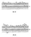
- FIG. 8Aillustrates one embodiment of a front illumination apparatus 100 that can be used to illuminate an array of display elements or modulating elements 130 in a display device.
- the light modulating elements 130may comprise, e.g., interferometric modulators, electrophoretic or reflective LCD elements, etc. and may be disposed on a substrate. This substrate may be used to support the modulating elements during fabrication.
- the substratemay comprise, for example, glass or plastic, although other materials may be used.
- the illumination apparatus 100can include a light guide 110 comprising, for example, one or more films, film stacks, layers, sheets, or slab-like components disposed in front of the array of modulating elements 130 .
- the light guide 110comprises glass or plastic.
- the modulating elements 130are formed on a substrate and the light guide 110 is disposed on the opposite side of the substrate.
- the light guide 110may comprise one or more light guide layers formed on the side of the substrate opposite to the modulating elements.
- This light guide 110has a first end 110 a and a second end 110 b . Light can be coupled into the light guide 110 at the first end 110 a and can propagate from the first end 110 a to the second end 110 b guided therein, for example, by total internal reflection.
- the light guide 110also has front and rear sides. The front side is farther from the modulating elements 130 while the rear side is closer to the light modulating elements.
- This illumination apparatus 100further comprises a multilayer stack with a holographic layer 120 configured to direct light propagating in the light guide 110 onto the modulating elements 130 .
- This holographic layer 120may comprise one or more volume or surface holograms.
- the holographic layermay be referred to as diffractive optics, comprising for example diffractive features such as volume or surface features.
- the diffractive opticscomprises one or more holograms.
- the diffractive features in such embodimentscomprise holographic features.
- Holographyadvantageously enables light to be manipulated so as to achieve a desired output for a given input.
- multiple functionsmay be included in a single holographic layer.
- a first hologramcomprising a first plurality of holographic features that provide for one function (e.g., turning light) and a second hologram comprising a second plurality of holographic features provide for another function (e.g. collimating light).
- the holographic layer 120may comprise a first set of volume index of refraction variations or topographical features arranged to diffract light in a specific manner, for example, to turn light propagating across the light guide 110 into the array of light modulating elements 130 as well as a second set of volume index of refraction or topographical variations arranged to diffract light, for example, to collimate light.
- a holographic layermay be equivalently considered by one skilled in the art as comprising multiple holograms or as comprising a single hologram having for example multiple optical functions recorded therein.
- the term hologrammay be used herein to describe diffractive optics in which one or more optical functions have been holographically recorded.
- a single holographic layermay be described herein as having multiple holograms recorded therein each providing a single optical function such as, e.g., collimating light, etc.
- the holographic layermay be attached to the illumination apparatus 100 with an adhesive such as a pressure sensitive adhesive (PSA), or other adhesive.
- PSApressure sensitive adhesive
- the adhesiveis index matched or has an index similar to the holographic layer.
- Other methodsmay be used to attach the holographic layer to the illumination apparatus.
- the holographic layer 120 shown in FIG. 8Ais disposed on the front side of the light guide 130 and comprises a reflective hologram.
- the reflective holographic layer 120 of FIG. 8Areflects light within an angular range of acceptance toward the light modulating elements 130 . This light may be directed substantially normal to the holographic layer 120 and the light modulating elements 130 .
- light diffracted by the hologrammay be directed into a range of angles having an angular width of full width at half maximum (FWHM) between about 2° to 10°, 10° to 20°, 20° to 30°, 30° to 40°, 40° to 50° and may be centered at an angle of about 0 to 5°, 5°-10°, 10° to 15°, 15° to 20°, 20° to 25° with respect to the normal to the holographic layer. Accordingly, although FIG.
- FWHMfull width at half maximum
- Light directed at other angles outside the range of acceptance angles of the holographic layeris reflected at an angle generally equal to the angle of incidence in some embodiments.
- This lightmay, for example, be reflected by total internal reflection from an interface between the holographic layer 120 and the light guide layer 110 , for example, where the light guide layer has a higher index of refraction than the holographic layer, and the holographic layer is an optical isolation layer for the light guide.
- light incident at angles outside the acceptance rangeis transmitted through the holographic layer 120 , and reflected from a surface on the reverse side of the hologram 120 .
- the lightmay be totally internally reflected at the interface between the holographic layer 120 and surrounding medium (e.g., air), for example, in the case where the holographic layer has a high index of refraction relative to the light guide.
- the surface of the holographic layer 120 away from the light guidemay be coated with a reflective layer comprising, for example, a metal, such as aluminum, or a dielectric material to provide reflection.
- a reflective layercomprising, for example, a metal, such as aluminum, or a dielectric material to provide reflection.
- Other approaches to introducing reflectionare additionally or alternatively possible.
- the acceptance rangemay be centered at angles of about 5, about 10, about 15, about 20, about 25, about 30, about 35, about 40, about 45, about 50, about 55, about 60, about 65, about 70, about 75, about 80, or about 85 degrees, and may have a width (FWHM, for example) of about 1, about 2, about 4, about 5, about 7, about 10, about 15, about 20, about 25, about 30, about 35, about 40, or about 45 degrees.
- the efficiency of the hologram 120may vary for different embodiments.
- the efficiency of a hologramis the ratio of (a) light incident within the acceptance range which is redirected (e.g., turned) by the hologram as a result of optical interference caused by the holographic features to (b) the total light incident within the range of acceptance, and is determined by the design and fabrication parameters of the hologram 120 .
- the efficiencyis greater than about 1%, about 5%, about 10%, about 15%, about 20%, about 25%, about 30%, about 35%, about 40%, about 45%, about 50%, about 55%, 60%, about 65%, about 70%, about 75%, about 80%, about 85%, about 90%, or about 95%.
- optical isolation region 140having a lower refractive index than the light guide 110 is also shown.
- This low refractive index region 140may act as an optical isolation layer for the light guide 110 .
- the interface of light guide 110 and low n layer 140forms a TIR (total internal reflection) interface.
- Light rays within the light guide 110 which are incident on the interface at greater than the critical angle (e.g., 40°), as measured with respect to the normal to the surface,will be specularly reflected back into the light guide 110 .
- the low n region 140has an index of refraction, n, less than the index of refraction of the light guide 110 , and may, for example be a layer of material such as a layer of glass or plastic. Other materials may also be used. In various preferred embodiments, the material is substantially optically transparent such that the display elements 130 may be viewed through the material.
- the low n region 140advantageously isolates the light propagating across the light guide 110 from the modulating elements 130 unless the light is turned by the holographic layer 120 through the low n region 140 into the modulating elements.
- the light modulating elements 130are absorbing of at least some wavelengths or wavelength bands. Without the low n region 140 , also referred to as an optical isolation region, light propagating across the light guide 110 might be lost to absorbing light modulating elements 130 located adjacent to the light guide.
- the low index region 140comprises an air gap or a gap filled with another gas or liquid.
- the light guide 110 and hologram 120may be separated from the display elements 130 by the gap filled with air, gas, or other low index medium.
- the low index regioncomprises the substrate for the modulating elements 130 .
- the light guide 110may have an index of refraction higher than the substrate.
- light propagating through the light guide 110which is incident on the hologram 120 outside of the acceptance range, will continue to propagate across the surface of the display 100 .
- light propagating through the light guide 110which is incident on the hologram 120 within the acceptance range, will be turned so as to leave the holographic layer 120 and be incident on the low n layer 140 at about 90 degrees with respect to the holographic layer.
- the turned lightwill be transmitted through the low n layer 140 to illuminate the light modulators 130 .
- FIG. 8Bis a cross section of another embodiment of an illumination apparatus 100 for a display device.
- the apparatus 100comprises a light guide 110 , holographic layer 120 , and low n isolation layer 140 , which are each disposed forward an array of light modulators 130 .
- the holographic layer 120comprises a transmissive hologram.
- the holographic layer 120is configured to transmit light incident within the acceptance range and direct this transmitted light substantially perpendicular to holographic layer 120 and the light modulators 130 . Accordingly, the light guide 110 is in front of the holographic layer 120 while the light modulators 130 are rearward of the holographic layer.
- TIR interfacesare located at the interface between the light guide 110 and the front surface of the holographic layer 120 and at the interface between the light guide 110 and the medium (e.g., air) adjacent the illumination apparatus 100 .
- Another low index layer(not shown) in front of the light guide 110 may also be used.
- the interface between the holographic layer 120 and the optical isolation layer 140form a TIR interface for guiding light within the light guide 110 .
- lightpropagates along the light guide from the first end to the second end via total internal reflection.
- Light incident on the holographic layer 120 at an angle within the range of acceptanceis transmitted through the holographic layer 120 at normal incidence to the light modulating elements 130 .
- This lightpasses through the low index isolation layer 140 to the light modulators 130 .
- FIG. 8Cis a cross section of another embodiment of an illumination apparatus 100 for a display device with a multilayer stack comprising a light guide 110 , holographic layer 120 , and low index isolation layer 140 disposed forward of an array of display elements 130 .
- the display elements 130are light modulators 130 .
- the light guide 110has front and rear portions 110 A and 110 B, where the front light guide portion 110 A is forward of the holographic layer 120 and the rear light guide portion 110 B is rearward of the holographic layer 120 . (These front and rear portions 110 A and 110 B may be referred to as light guides themselves.) As illustrated, the light modulators 130 are also rearward of the holographic layer 120 .
- the front and rear portions 110 A, 110 B of the light guide 110may comprise light guide films that sandwich the holographic layer 120 therebetween.
- the hologram(s) or holographic featuresmay be recorded in the holographic layer 120 after the layer is sandwiched between the front and rear portions 110 A, 110 B.
- each of the light guide portions 110 A and 110 Bhas a TIR surface.
- the light guide portion 110 Ahas a TIR surface in the front of the front light guide portion 110 A
- the light guide portion 110 Bhas a TIR surface at the rear of the rear light guide portion 110 B.
- the TIR surface in the front of the front light guide portion 110 Ais formed by the interface with the external medium (e.g., air) or with another low index layer in front of the front portion 110 A.
- the TIR surface at the rear of the rear light guide portion 110 Bis formed by the interface of the low index isolation layer 140 with the light guide portion 110 B.
- the holographic layer 120comprises holographic features configured to turn and transmit light incident within a first acceptance range from light guide portion 110 A, and to turn light incident within a second acceptance range from light guide portion 110 B.
- the first angleis for light propagating within the front light guide portion 110 A incident on the holographic layer 120 and the second angle is for the light propagating in the rear light guide portion 110 B that is incident on the holographic layer.
- FIG. 8Clight from light guide portion 110 A is turned and transmitted through the holographic layer 120 , through light guide portion 110 B and to the light modulators 130 . Additionally, light from light guide portion 110 B is turned and reflected from the holographic layer 120 , through light guide portion 110 B, and to the light modulators 130 .
- multiple hologram o sets of holographic featuresmay be recorded within the holographic layer 120 .
- Such holograms or holographic featurescan be recorded by using beams directed at different angles.
- a holographic recording mediummay be exposed to one set of beams to establish a reflection hologram.
- the holographic recording mediummay additionally be exposed to a second set of beams to record a transmission hologram.
- the holographic recording mediummay be developed such that the two holograms are formed, for example, in a single layer. In such an arrangement, two sets of holographic features, one corresponding to the reflection hologram and one corresponding to the transmission hologram are formed. (One skilled in the art may refer to the aggregate structure as a single hologram or alternately as multiple holograms.)
- Optical or non-optical replication processesmay be employed to generate additional holograms.
- a mastercan be generated from the developed layer and the master can be used to produce similar holograms having the two sets of holographic features therein to provide the reflective and transmissive functionality such as shown in FIG. 8 .
- Intermediate structuresmay also be formed.
- the originalcan be replicated one or more times before forming the master or product.
- the replicated holographic structuremay be referred to as a single hologram comprising multiple sets of holographic features that provide different functions.
- the sets of holographic features providing different functionscan be referred to as different holograms.
- the holographic featuresmay comprise, for example, surface features or volume features of the holographic layer 120 . Other methods can also be used.
- the hologramsmay for example be computer generated or formed from a master. The master may or may not be computer generated. In some embodiments, different methods or a combination of methods are used.
- the first and second acceptance rangeshave substantially the same magnitude but different signs.
- the first acceptance rangeis centered at about 20 degrees and is about 4 degrees wide and the second acceptance range is centered at about ⁇ 20 degrees and is about 4 degrees wide.
- Other anglesare possible.
- only one hologram configured to turn the light to the modulatorsis recorded (reflective or transmissive).
- only reflection holograms configured to turn the light to the modulatorsare recorded in the holographic layer 120 .
- only transmissive holograms configured to turn the light to the modulatorsare recorded.
- holographic layer 120may also be configured to collimate and/or diffuse ambient light incident thereon. Other features may additionally be included.
- a hologramAs mentioned above, a hologram, or its holographic features, has a limited efficiency. Accordingly, only a portion of the light within the acceptance range is turned toward the light modulators 130 . The un-turned portion reflects from or is transmitted through the holographic layer 120 at an angle of reflection or angle of transmission having substantially the same magnitude as the angle of incidence on the holographic layer.
- the holographic layermay act as an optical isolation layer for the light guides in some embodiments, although in others the light may pass through to the holographic layer if not within the range of acceptance angles. Accordingly, the transmitted or reflected light will continue to propagate within the light guide 110 totally internally reflecting from an interface of the light guide 110 . Accordingly, this light will again be directed back towards the holographic layer 120 .
- the power of the light turned at the second turningis less than that of the first turning.
- the efficiency of the hologram 120is 50%
- 50% of the incident light within the acceptance rangeis turned toward the light modulators 130 on the first pass
- 50% of the incident light within the acceptance rangecontinues to propagate across the display 100 .
- the propagated 50%interacts with the holographic layer 120 on the second pass.
- 50% efficiency of the hologram50% of the propagated 50% is turned, and 50% of the propagated 50% continues to propagate along the light guide.
- light directed to the modulating elements on the second passhas 25% of the optical power of the original light incident on the holographic layer on the first pass.
- the propagated light after the second passhas 25% of the optical power of the original light incident on the holographic layer on the first pass.
- 50%is turned at the first pass
- 25%is turned upon the second pass
- 12.5%is turned upon the third pass, and so forth. This effect is problematic as the result is that one side of the screen is brighter than the other.
- Additional hologramsmay be recorded in the holographic layer 120 for the different embodiments described herein. These holograms may correspond to different angles of incidence, transmission, and/or reflection. Accordingly, a variety of acceptance angles may be provided. Similarly, the additional holograms provide different angles at which light is directed to the light modulating elements 130 .
- additional hologramsmay introduce diffusion.
- One or more holographic diffusersmay be recorded in the holographic layer 120 .
- the holographic layer 120may thus operate as a diffuser in front of the light modulating elements 130 .
- the diffusermay reduce the specular or mirror-like appearance of certain modulating devices such as interferometric modulators.
- the diffusermay also reduce the pixilation of some light modulator arrays.
- the diffusermay also alter the angle of propagation of light within the light guide, such that after interacting with the diffuser, the light is within the angle of acceptance of the holographic layer.
- Such holographic diffusersmay be formed optically, may be computer-generated, or may be formed by using other approaches. Other functionalities can be added by recording additional holograms in the layer.
- the holographic layer 120may be disposed directly on the substrate on which the light modulating elements 130 are formed.
- the holographic layer 120may be formed on a front side of the substrate and the light modulating elements 130 may be formed on a rear side of the substrate.
- the substratemay form all or port of the light guide.
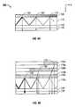
- FIG. 9Ais a cross section of one embodiment of an illumination apparatus 200 comprising a light guide 110 , holographic layer 120 , and low n layer 140 disposed in front of light modulators 130 .
- the embodiment of FIG. 9Ais similar to that shown in FIG. 8A .
- FIG. 9Aillustrates the operation of the light guide 110 , low index layer 140 , and holographic layer 120 , which propagate light across the array of light modulators 130 .
- the holographic layer 120distributes light propagated along the light guide 110 so as to provide substantially uniform brightness to the array of light modulating elements 130 .
- the hologrammay have a uniform efficiency and a varying range of acceptance angles.
- the range of acceptance anglesmay be narrow. Further away from the light source, the range of acceptance angles turned by the hologram may broaden and hence increase the amount of light turned by the hologram.
- some combination of efficiency and acceptance anglemay be arranged in order to uniformly direct light to the array of light modulating elements 130 .
- the holographic layer 120is configured to have increasing efficiency across the length (x direction) of the light guide 100 .
- the increased efficiencymay be introduced by increasing the diffraction efficiency of the holographic layer 120 , which is schematically indicated in FIG. 9A by increasingly dense hatching in the holographic layer 120 .
- the holographic layer 120can be formed such that the efficiency at the first pass 150 is 20%, the efficiency at the second pass 160 is 25%, and the efficiency at the third pass is 33%. Accordingly of the power of the light incident on the holographic layer 120 at the first location 150 , 20% is turned and 80% is propagated. At the second location 160 , 80% of the original light in the range of acceptance angles is incident.
- the efficiency of the holographic layer 120 at the second location 160is 25%, 20% of the original light is turned, and 60% is propagated.
- the efficiency at the third location 170is 33%, 20% of the original light is turned, and 40% is propagated.
- the hologram 120is formed with varying efficiency across the length of the light guide 110 , the amount of light turned at each location 150 , 160 , 170 is 20% of the original light incident on the holographic layer 120 within the range of acceptance angles. Accordingly, the brightness does not vary across the array of modulating elements 130 .
- a hologram having progressively increasingly efficiency across its spatial extentmay be formed, for example, by using a beam having a gradient in intensity across its width in the recording process. Such a gradient intensity can be obtained by using a neutral density filter having a gradient in optical density. Other methods may be used to produce the hologram.
- the hologramsmay be computer generated. The holograms may also be produced using a master.
- FIG. 9Bshows another structure which can be used additionally or alternatively to vary the efficiency of the holographic layer 120 .
- the light guide 110has layers 110 A, 110 B, and 110 C
- the holographic layer 120has stacked layered portions 120 A, 120 B, and 120 C.
- Increased hologram efficiencyis achieved, at least in part, by adding additional layered portions and arranging the stacked portions such that the number of stacked holographic portions or the total thickness of the layered holographic portions is smaller at the first end of the light guide and increases along the length of the holographic layer to the second end of the light guide. Accordingly, light injected into the light guide 110 has increased opportunity to be diffracted at locations closer to the second end where the optical power within the light guide will be less.
- the efficiency of the holographic layer 120 at the first location 150a portion of the incident light is turned and a portion continues to propagate along the light guide 110 (e.g. light guide portion 110 c ).
- the lightis incident on a holographic multilayer comprising two sublayers, and a higher effective efficiency is thereby achieved.
- the lightis incident a holographic multilayer comprising in addition to the two sublayers, a third sublayer to effectively further increase the turning efficiency.
- the hologram layers 120 A, 120 B, and 120 Care each formed, their respective individual efficiencies can be tailored such that the effective combined efficiencies at each turning may produce substantially identical portions of turned light.
- FIG. 9Bonly shows a few rays traced for illustrative purposes and does not represent a complete picture of the effect on the light of each reflection at each layered holographic portion. Nevertheless, rays not shown are also affected by the progression in optical efficiency and thus may further contribute to the uniformity of light across the array of modulating elements. Additionally, in other embodiments, more (or fewer) sublayers may be used.
- the array of light modulating elementscan be substantially uniformly illuminated.
- the efficiencymay increase from 0-5 to 10-50% across a distance of 0-10 to 25-50 mm. Accordingly, the efficiency may increase at a rate of 0.1 to 2%/mm.
- This gradationcan be smooth or a step-like progression. The steps may be about 5 mm wide.
- the resultant uniformity of light turned out of the light guidemay be 20 to 80% across a length of 0 to 50 mm.
- FIG. 10Ashows an embodiment of an illumination apparatus 200 comprising a holographic layer 220 , a light guide 210 , and low n layer 240 , in front of a plurality of light modulators 230 .
- the light modulators 230may comprise interferometric modulators having reflective surfaces such as are described above.
- the holographic layer 220is configured to substantially collimate ambient light incident on the holographic layer from a range of angles.
- Certain modulating elements 230such as interferometric modulators modulated light rays normal to the modulators. Other rays may be absorbed and not contribute to the image formation.
- the incident light that is used for near normal viewing of the image displayis increased. Accordingly, the brightness of the displayed image when viewed at near normal is increased using ambient light.
- collimated rays directed at generally normal incidence onto the modulatorsmay be oriented within about ⁇ 10 degrees of the normal to said modulators. Additionally, in some embodiments only a portion of the ambient light, for example, 70% to 50%, 60% to 40%, 50% to 30%, 40% to 20%, or 30% to 10% or less may be collected and collimated by the hologram. For example, in many display applications, ambient light overhead can be collected and used whereas ambient light from below is blocked by the user.
- the holographic layermay be configured, for example, to collect light from an angular range of between about 45° to 90° with respect to the normal to the holographic layer 220 and redirect the rays into a range of between about 0° to about 40° with respect to the normal, or in other embodiments between about 0° to about 20°. Other ranges are also possible.
- FIG. 10Aadditionally shows an optional prismatic turning film 201 that can be disposed on the holographic layer 220 .
- the prismatic turning film 201can be used to turn light propagating along the length (x direction) of light guide 210 toward the display elements (in the z direction) such that the light is substantially normal to the array of display elements.
- FIG. 10Bshows an embodiment of an illumination apparatus 250 which includes first and second holograms 220 A and 220 B and first and second light guide portions 210 A, 210 B, on which said first and second holograms are disposed, and a low index isolation layer 240 in front of a plurality of light modulators 230 .
- the first hologram 220 Ais disposed in front of the first light guide portion 210 A.
- the first light guide portion 210 Ais disposed in front of the second hologram 220 B
- the second hologram 220 Bis disposed in front of the second light guide portion 210 B, which is disposed in front of the optical isolation layer 240 and the light modulating elements 230 .
- the second hologram 220 B of display 250is configured to collect ambient light incident thereon over a range of non-normal angles and to collimate and direct the collected light substantially normal to the light modulating elements 230 , as described above with respect to hologram 220 of apparatus 200 shown in FIG. 10A .
- the ambient light brightnessis increased by the second hologram 220 B.
- first hologram 220 Ais configured to turn light of a certain acceptance angle range such that it is substantially perpendicular to the light modulator layer 230 .
- the second hologram 220 Amay have similar configuration and function as hologram 120 according to various embodiments described above.
- FIG. 10Cshows an embodiment of a display 300 which has a single holographic layer 320 , a light guide 310 , and a low index isolation layer 340 disposed in front of the light modulators 330 .
- the light guide 310 , low n layer 340 , and light modulators 330have functionality and structure which may be similar to that of similar structures described above.
- the holographic layer 320comprises first and second holograms or sets of holographic features having the functions described above with reference to holograms 220 A and 220 B, respectively shown in FIG. 10B . These first and second holograms or sets of holographic features can be recorded in the same holographic medium. Optical recording by using two different optical set-ups: one wherein wide angle illumination representing ambient lighting is used and one where light is propagated along the light guide. Other methods may also be used to record the multiple holographic features in the holographic layer 320 .
- the holographic featuresmay, for example, be computer generated. Additionally, one or more holographic masters may be used.
- the first hologram or set of holographic featuresis configured to turn light propagating within the light guide 310 normal to the light modulating elements 330 .
- the second holographic featureis configured to collect a wide range of angles of ambient light and direct the light onto the modulating elements 330 at substantially normal incidence thereto.
- the first hologram or set of holographic featuresmay also collimate the light. Accordingly, the display device has holographically enhanced display brightness characteristics similar to that described above with reference to FIG. 10B .
- the first and second holographic featuresmay be integrated in a single holographic layer 320 . In some embodiments, an additional holographic feature may be included.
- a third hologram or set of holographic features which diffuses light reflected from the modulatorsmay be included.
- the third set of holographic featuresmay be integrated with any of the other sets of holographic features.
- the third set of holographic featureis disposed in a separate holographic layer.
- FIG. 10Dshows an embodiment of a display 350 which has first and second holograms 320 A and 320 B, disposed on first and second light guides portions 310 A and 310 B, respectively, and low index isolation layer 340 , disposed in front of light modulators 330 .
- the light guides portions 310 A and 310 B, low index layer 340 , and light modulators 330have functionality and structure which may be similar to that of similar elements described above.
- the first and second holograms 320 A and 320 Bcooperatively increase the brightness of the display 350 .
- the first hologram 320 Ahas functionality similar to the holographic layer 320 described above in reference to FIG. 10C .
- the first hologram 320 Ais configured to collimate ambient light and direct the light into a narrower range of angles that are directed more normal to the plurality of modulating elements.
- the second hologram 320 Bis configured to further collimate light incident to it.
- the second hologram 320 Bis configured to receive a range of angles and to transmit that light into a smaller range of angles directed to the light modulators 330 . This transmitted range of angles is also substantially centered substantially normal to the light modulating elements.
- holograms 320 A and 320 Bcooperatively increase the brightness of the display 350 by increasing the collimation of ambient light and increasing steepness of the angle at which ambient light incident on the hologram 320 A is directed into light modulators 330 .
- hologram 320 Apartially collimates light from wide angles and transmits the light to hologram 320 B, which is configured to further collimate the light and transmit it to the light modulators 330 at substantially normal angles.
- the first hologram 320 Aturns the light into a range of angles substantially normal to the light modulating elements.
- the second hologram 320 Breceived this light and transmits the light into a narrower range of angles.
- the hologram 320 Bfurther collimates the turned light so that it is incident on the light modulators 330 , has a greater intensity, and is substantially normal to the light modulating elements. Brightness is thereby increased.
- a holographic diffusercan also be incorporated into the light apparatus of any of the embodiments in FIGS. 1A-10D .
- This holographic diffusermay be included on a separate layer or may be recorded on one of the holographic layers already present.
- the holographic diffusermay have a limited field of view into which light from the light modulating elements is scattered so as to increase brightness. A viewer will typically view the display device and the light modulating elements from a limited number of viewing positions and angles. Accordingly, in some embodiments, the diffuser need not scatter light into a large range of angles.
- FIG. 10Eshows an embodiment of a display 400 which has a single holographic layer 320 , a light guide 310 , and a low index isolation layer 340 disposed in front of the light modulators 330 .
- the light guide 310 , low n layer 340 , and light modulators 330have functionality and structure which may be similar to that of similar structures described above.
- the holographic layer 320comprises first and second holograms or sets of holographic features configured to turn light from the light guide 310 toward the light modulators 330 and configured to diffuse light incident thereon. These first and second holograms or sets of holographic features can be recorded in the same holographic layer. Optical recording by using two different optical set-ups: one representing light directed to a viewer is used and one where light is propagated along the light guide. Other methods may also be used to record the multiple holograms or sets of holographic features in the holographic layer 320 .
- the holograms or holographic featuresmay, for example, be computer generated. Additionally, one or more holographic masters may be used. The master may or may not be computer generated.
- the first and second holograms or sets of holographic featuresare disposed in first and second layers, respectively.
- the first holographic featureis configured to turn light propagating within the light guide 310 normal to the light modulating elements 330 .
- the second holographic featureis configured to diffuse light reflected from the modulating elements 330 .
- a third hologram or set of holographic featuresmay additionally collimate the light. Accordingly, the display device has holographically enhanced display lighting characteristics.
- the first and second holograms or sets of holographic featuresmay be integrated in a single holographic layer 320 .
- FIG. 11Ais a top view of a light source 400 disposed with respect to a light guide 410 to inject light along the width of the light guide.
- FIG. 11Bis a perspective view showing the light source 400 disposed at an edge of the light guide 410 to edge couple light therein.
- the light guide 410comprises a hologram portion 420 that includes a hologram configured to receive light injected by the edge coupled light source 400 and to turn the light such that the light propagates along the length (x direction) of the light guide 410 .
- the hologramis also configured to distribute the light along the width (y direction) of the light guide 410 .
- FIG. 11Aalso shows the line I-I, which defines a cross section across the light guide.
- the light guide 410can have a cross-section I-I similar to the cross sections shown in any of FIGS. 8-10 depending on the configuration.
- the hologram in hologram portion 420is configured to turn light of a range of angles into a narrower set of angles such that light propagating along the length of the light guide is substantially collimated. Additionally, the distribution of rays is substantially parallel to the length-wise direction (x) of the light guide 410 .
- FIG. 11Cshows one method of optically recording a hologram for the hologram portion 420 .
- a reference light source 400 ′injects a light beam into a light guide 410 ′ along the width (y direction). This light beam may include a wide range of angles.
- a more collimated light sourceis disposed with respect to the light guide 410 ′ such that collimated rays 430 are injected into the light guide 410 ′ along the length-wise direction (x) of a light guide.
- the light guide 410 ′includes a film in the portion of the light guide where the two beams intersect. This film is developed to produce a hologram or a master.
- additional functionalitymay be incorporated into the diffractive optics with additional holographic recordings. Other methods may be used to produce the hologram.
- the hologrammay be computer generated.
- Films, layers, components, and/or elementsmay be added, removed, or rearranged. Additionally, processing steps may be added, removed, or reordered.
- film and layerhave been used herein, such terms as used herein include film stacks and multilayers. Such film stacks and multilayers may be adhered to other structures using adhesive or may be formed on other structures using deposition or in other manners.
- sets of holographic features providing multiple functionalitymay integrated together in a single layer or in multiple layers. Multiple sets of holographic features included in a single layer to provide multiple functionality may be referred to as a plurality of holograms or a single hologram.
Landscapes
- Physics & Mathematics (AREA)
- General Physics & Mathematics (AREA)
- Optics & Photonics (AREA)
- Mechanical Light Control Or Optical Switches (AREA)
- Optical Couplings Of Light Guides (AREA)
- Holo Graphy (AREA)
- Diffracting Gratings Or Hologram Optical Elements (AREA)
Abstract
Description
Claims (25)
Priority Applications (1)
| Application Number | Priority Date | Filing Date | Title |
|---|---|---|---|
| US12/419,263US8368981B2 (en) | 2006-10-10 | 2009-04-06 | Display device with diffractive optics |
Applications Claiming Priority (3)
| Application Number | Priority Date | Filing Date | Title |
|---|---|---|---|
| US85075906P | 2006-10-10 | 2006-10-10 | |
| PCT/US2007/021623WO2008045463A2 (en) | 2006-10-10 | 2007-10-09 | Display device with diffractive optics |
| US12/419,263US8368981B2 (en) | 2006-10-10 | 2009-04-06 | Display device with diffractive optics |
Related Parent Applications (1)
| Application Number | Title | Priority Date | Filing Date |
|---|---|---|---|
| PCT/US2007/021623ContinuationWO2008045463A2 (en) | 2006-10-10 | 2007-10-09 | Display device with diffractive optics |
Publications (2)
| Publication Number | Publication Date |
|---|---|
| US20090251752A1 US20090251752A1 (en) | 2009-10-08 |
| US8368981B2true US8368981B2 (en) | 2013-02-05 |
Family
ID=39092712
Family Applications (2)
| Application Number | Title | Priority Date | Filing Date |
|---|---|---|---|
| US12/444,683AbandonedUS20100103488A1 (en) | 2006-10-10 | 2007-10-09 | Display device with diffractive optics |
| US12/419,263Expired - Fee RelatedUS8368981B2 (en) | 2006-10-10 | 2009-04-06 | Display device with diffractive optics |
Family Applications Before (1)
| Application Number | Title | Priority Date | Filing Date |
|---|---|---|---|
| US12/444,683AbandonedUS20100103488A1 (en) | 2006-10-10 | 2007-10-09 | Display device with diffractive optics |
Country Status (3)
| Country | Link |
|---|---|
| US (2) | US20100103488A1 (en) |
| EP (2) | EP1958010A2 (en) |
| WO (2) | WO2008045463A2 (en) |
Cited By (4)
| Publication number | Priority date | Publication date | Assignee | Title |
|---|---|---|---|---|
| US20120069031A1 (en)* | 2007-12-07 | 2012-03-22 | Qualcomm Mems Technologies, Inc. | Decoupled holographic film and diffuser |
| US20140176671A1 (en)* | 2012-12-26 | 2014-06-26 | Lg Display Co., Ltd. | Apparatus for displaying a hologram |
| US8902484B2 (en) | 2010-12-15 | 2014-12-02 | Qualcomm Mems Technologies, Inc. | Holographic brightness enhancement film |
| US20150130896A1 (en)* | 2013-11-08 | 2015-05-14 | Qualcomm Mems Technologies, Inc. | Light redirection hologram for reflective displays |
Families Citing this family (35)
| Publication number | Priority date | Publication date | Assignee | Title |
|---|---|---|---|---|
| US8928967B2 (en) | 1998-04-08 | 2015-01-06 | Qualcomm Mems Technologies, Inc. | Method and device for modulating light |
| WO1999052006A2 (en) | 1998-04-08 | 1999-10-14 | Etalon, Inc. | Interferometric modulation of radiation |
| TWI289708B (en) | 2002-12-25 | 2007-11-11 | Qualcomm Mems Technologies Inc | Optical interference type color display |
| US7342705B2 (en) | 2004-02-03 | 2008-03-11 | Idc, Llc | Spatial light modulator with integrated optical compensation structure |
| US7813026B2 (en) | 2004-09-27 | 2010-10-12 | Qualcomm Mems Technologies, Inc. | System and method of reducing color shift in a display |
| US7710636B2 (en)* | 2004-09-27 | 2010-05-04 | Qualcomm Mems Technologies, Inc. | Systems and methods using interferometric optical modulators and diffusers |
| US7630123B2 (en) | 2004-09-27 | 2009-12-08 | Qualcomm Mems Technologies, Inc. | Method and device for compensating for color shift as a function of angle of view |
| US7508571B2 (en) | 2004-09-27 | 2009-03-24 | Idc, Llc | Optical films for controlling angular characteristics of displays |
| US7916980B2 (en) | 2006-01-13 | 2011-03-29 | Qualcomm Mems Technologies, Inc. | Interconnect structure for MEMS device |
| US7603001B2 (en) | 2006-02-17 | 2009-10-13 | Qualcomm Mems Technologies, Inc. | Method and apparatus for providing back-lighting in an interferometric modulator display device |
| US7766498B2 (en) | 2006-06-21 | 2010-08-03 | Qualcomm Mems Technologies, Inc. | Linear solid state illuminator |
| US7845841B2 (en) | 2006-08-28 | 2010-12-07 | Qualcomm Mems Technologies, Inc. | Angle sweeping holographic illuminator |
| US8107155B2 (en) | 2006-10-06 | 2012-01-31 | Qualcomm Mems Technologies, Inc. | System and method for reducing visual artifacts in displays |
| EP1943555B1 (en) | 2006-10-06 | 2012-05-02 | QUALCOMM MEMS Technologies, Inc. | Optical loss structure integrated in an illumination apparatus of a display |
| EP1943551A2 (en) | 2006-10-06 | 2008-07-16 | Qualcomm Mems Technologies, Inc. | Light guide |
| US7855827B2 (en) | 2006-10-06 | 2010-12-21 | Qualcomm Mems Technologies, Inc. | Internal optical isolation structure for integrated front or back lighting |
| EP2069838A2 (en) | 2006-10-06 | 2009-06-17 | Qualcomm Mems Technologies, Inc. | Illumination device with built-in light coupler |
| EP1958010A2 (en) | 2006-10-10 | 2008-08-20 | Qualcomm Mems Technologies, Inc | Display device with diffractive optics |
| US7864395B2 (en) | 2006-10-27 | 2011-01-04 | Qualcomm Mems Technologies, Inc. | Light guide including optical scattering elements and a method of manufacture |
| US7777954B2 (en) | 2007-01-30 | 2010-08-17 | Qualcomm Mems Technologies, Inc. | Systems and methods of providing a light guiding layer |
| US8654061B2 (en) | 2008-02-12 | 2014-02-18 | Qualcomm Mems Technologies, Inc. | Integrated front light solution |
| WO2009102731A2 (en) | 2008-02-12 | 2009-08-20 | Qualcomm Mems Technologies, Inc. | Devices and methods for enhancing brightness of displays using angle conversion layers |
| WO2009102733A2 (en)* | 2008-02-12 | 2009-08-20 | Qualcomm Mems Technologies, Inc. | Integrated front light diffuser for reflective displays |
| WO2009129264A1 (en)* | 2008-04-15 | 2009-10-22 | Qualcomm Mems Technologies, Inc. | Light with bi-directional propagation |
| US20090323144A1 (en)* | 2008-06-30 | 2009-12-31 | Qualcomm Mems Technologies, Inc. | Illumination device with holographic light guide |
| US20100238529A1 (en)* | 2009-03-23 | 2010-09-23 | Qualcomm Mems Technologies, Inc. | Dithered holographic frontlight |
| CN102449512A (en) | 2009-05-29 | 2012-05-09 | 高通Mems科技公司 | Illumination devices and methods of fabrication thereof |
| US20120120467A1 (en)* | 2010-11-17 | 2012-05-17 | Qualcomm Mems Technologies, Inc. | Hybrid light guide with faceted and holographic light turning features |
| RU2015108650A (en)* | 2012-08-13 | 2016-10-10 | Байер Матириальсайенс Аг | Light guide panel with outlet elements |
| US9835786B2 (en)* | 2012-08-15 | 2017-12-05 | Apple Inc. | Display backlight with diffractive and refractive light scattering structures |
| US20160041323A1 (en)* | 2014-08-08 | 2016-02-11 | Qualcomm Mems Technologies, Inc. | Light extracting diffusive hologram for display illumination |
| US10591804B2 (en)* | 2015-03-30 | 2020-03-17 | Luminit Llc | Quantum wave-converter |
| KR102409393B1 (en)* | 2017-08-14 | 2022-06-15 | 삼성전자주식회사 | Light guide plate, backlight unit, and holographic display device having the same |
| KR102846679B1 (en)* | 2018-12-26 | 2025-08-18 | 엘지전자 주식회사 | Electronic device |
| GB201903708D0 (en)* | 2019-03-19 | 2019-05-01 | Wave Optics Ltd | Improved angular uniformity waveguide for augmented or virtual reality |
Citations (393)
| Publication number | Priority date | Publication date | Assignee | Title |
|---|---|---|---|---|
| US2518647A (en) | 1948-01-07 | 1950-08-15 | Celanese Corp | Interferometer means for thickness measurements |
| US3813265A (en) | 1970-02-16 | 1974-05-28 | A Marks | Electro-optical dipolar material |
| US4378567A (en) | 1981-01-29 | 1983-03-29 | Eastman Kodak Company | Electronic imaging apparatus having means for reducing inter-pixel transmission nonuniformity |
| DE3402746A1 (en) | 1984-01-27 | 1985-08-08 | Robert Bosch Gmbh, 7000 Stuttgart | Liquid crystal display |
| EP0278038A1 (en) | 1987-02-13 | 1988-08-17 | Battelle-Institut e.V. | Active flat type display panel |
| US4832459A (en) | 1984-02-06 | 1989-05-23 | Rogers Corporation | Backlighting for electro-optical passive displays and transflective layer useful therewith |
| US4850682A (en) | 1986-07-14 | 1989-07-25 | Advanced Environmental Research Group | Diffraction grating structures |
| US4863224A (en) | 1981-10-06 | 1989-09-05 | Afian Viktor V | Solar concentrator and manufacturing method therefor |
| US4915479A (en) | 1986-12-17 | 1990-04-10 | U.S. Philips Corporation | Liquid crystal display illumination system |
| US4918577A (en) | 1988-01-16 | 1990-04-17 | Alps Electric Co., Ltd. | Illumination light transmitting device |
| US4947291A (en) | 1988-06-17 | 1990-08-07 | Mcdermott Kevin | Lighting device |
| US4961617A (en) | 1989-07-19 | 1990-10-09 | Ferrydon Shahidi | Fibre optic waveguide illuminating elements |
| US5038224A (en) | 1989-12-22 | 1991-08-06 | Bell Communications Research, Inc. | Video imaging device in a teleconferencing system |
| US5042921A (en) | 1988-10-25 | 1991-08-27 | Casio Computer Co., Ltd. | Liquid crystal display apparatus |
| US5110370A (en) | 1990-09-20 | 1992-05-05 | United Solar Systems Corporation | Photovoltaic device with decreased gridline shading and method for its manufacture |
| US5151585A (en) | 1991-08-12 | 1992-09-29 | Hughes Danbury Optical Systems, Inc. | Coherent radiation detector |
| US5226099A (en) | 1991-04-26 | 1993-07-06 | Texas Instruments Incorporated | Digital micromirror shutter device |
| US5261970A (en) | 1992-04-08 | 1993-11-16 | Sverdrup Technology, Inc. | Optoelectronic and photovoltaic devices with low-reflectance surfaces |
| US5272496A (en) | 1991-08-06 | 1993-12-21 | Thomson-Csf | Image projector with optimized luminous efficiency |
| US5278680A (en) | 1989-10-05 | 1994-01-11 | Seiko Epson Corporation | Projection type liquid crystal display system and method of polarized light component projection |
| US5283600A (en) | 1992-02-21 | 1994-02-01 | Nec Corporation | LCD projector |
| US5289300A (en) | 1991-02-04 | 1994-02-22 | Semiconductor Energy Laboratory Co., Ltd. | Method of manufacturing electro-optical devices wherein the electrode is patterned on the modulation layer |
| WO1994006871A1 (en) | 1992-09-17 | 1994-03-31 | Canterbury Park Limited | A sign, a method of making the sign and an ink therefor |
| EP0590511A1 (en) | 1992-10-01 | 1994-04-06 | International Business Machines Corporation | Edge-lit transflective non-emissive display |
| GB2260203B (en) | 1991-10-04 | 1994-09-07 | Marconi Gec Ltd | Colour display system |
| US5361190A (en) | 1990-02-20 | 1994-11-01 | K. W. Muth Co. Inc. | Mirror assembly |
| GB2278222A (en) | 1993-05-20 | 1994-11-23 | Sharp Kk | Spatial light modulator |
| US5387953A (en) | 1990-12-27 | 1995-02-07 | Canon Kabushiki Kaisha | Polarization illumination device and projector having the same |
| US5387991A (en) | 1990-05-18 | 1995-02-07 | Canon Kabushiki Kaisha | Polarization converting device and polarized-light illuminating system using the device and image display unit using the device |
| US5398125A (en) | 1993-11-10 | 1995-03-14 | Minnesota Mining And Manufacturing Company | Liquid crystal projection panel having microlens arrays, on each side of the liquid crystal, with a focus beyond the liquid crystal |
| WO1995015582A1 (en) | 1993-12-02 | 1995-06-08 | R & S Renewable Energy Systems B.V. | A photovoltaic solar panel and a method for producing same |
| US5446510A (en) | 1989-12-20 | 1995-08-29 | Canon Kabushiki Kaisha | Image display apparatus |
| US5448659A (en) | 1993-02-01 | 1995-09-05 | Matsushita Electric Industrial Co., Ltd. | Waveguide-type image transmission device and fingerprint identification device |
| US5452385A (en) | 1993-03-09 | 1995-09-19 | Sharp Kabushiki Kaisha | Optical scanning device an optical scanning type display and an image data input/output device |
| US5459610A (en) | 1992-04-28 | 1995-10-17 | The Board Of Trustees Of The Leland Stanford, Junior University | Deformable grating apparatus for modulating a light beam and including means for obviating stiction between grating elements and underlying substrate |
| US5467417A (en) | 1992-09-16 | 1995-11-14 | Hitachi, Ltd. | Prism plate for efficiently emitting light flux within a predetermined range, and liquid crystal indicator and indicator illumination method using the same |
| US5481385A (en) | 1993-07-01 | 1996-01-02 | Alliedsignal Inc. | Direct view display device with array of tapered waveguide on viewer side |
| US5515184A (en) | 1991-11-12 | 1996-05-07 | The University Of Alabama In Huntsville | Waveguide hologram illuminators |
| US5517366A (en) | 1993-10-22 | 1996-05-14 | Olympus Optical Co., Ltd. | Concentric optical system |
| US5555186A (en) | 1994-02-15 | 1996-09-10 | Nec Corporation | Projection type liquid crystal display apparatus using multiple polarizing beam splitters |
| US5594830A (en) | 1992-03-23 | 1997-01-14 | Minnesota Mining And Manufacturing Co. | Luminaire device |
| US5601351A (en) | 1994-06-01 | 1997-02-11 | U.S. Philips Corporation | High-efficiency illumination device and image projection apparatus comprising such a device |
| US5626408A (en) | 1993-12-17 | 1997-05-06 | U.S. Philips Corporation | Illumination system for a color projection device and circular polarizer suitable for use in such an illumination system, and color image projection device comprising such an illumination system and circular polarizer |
| US5638084A (en) | 1992-05-22 | 1997-06-10 | Dielectric Systems International, Inc. | Lighting-independent color video display |
| US5647036A (en) | 1994-09-09 | 1997-07-08 | Deacon Research | Projection display with electrically-controlled waveguide routing |
| US5650865A (en) | 1995-03-21 | 1997-07-22 | Hughes Electronics | Holographic backlight for flat panel displays |
| US5659410A (en) | 1993-12-28 | 1997-08-19 | Enplas Corporation | Surface light source device and liquid crystal display |
| US5671314A (en) | 1993-01-15 | 1997-09-23 | Sisters Of Prividence In Oregon | Illuminator devices for ultraviolet light delivery and methods of making same |
| DE19622748A1 (en) | 1996-06-05 | 1997-12-11 | Forschungszentrum Juelich Gmbh | Interference filter based on porous silicon |
| US5703667A (en) | 1996-05-31 | 1997-12-30 | Shimada Precision, Co., Ltd. | Light guide plates and light guide plate assembly utilizing diffraction grating |
| US5735590A (en) | 1994-03-02 | 1998-04-07 | Tosoh Corporation | Backlighting device with a transparent sheet having straight ridges |
| US5749642A (en) | 1992-03-18 | 1998-05-12 | Canon Kabushiki Kaisha | Illuminating optical system and projector utilizing the same |
| US5771321A (en) | 1996-01-04 | 1998-06-23 | Massachusetts Institute Of Technology | Micromechanical optical switch and flat panel display |
| US5771124A (en) | 1996-07-02 | 1998-06-23 | Siliscape | Compact display system with two stage magnification and immersed beam splitter |
| US5772299A (en) | 1994-11-25 | 1998-06-30 | Lg Electronics Inc. | Optical apparatus for liquid crystal display projector |
| US5783614A (en) | 1997-02-21 | 1998-07-21 | Copytele, Inc. | Polymeric-coated dielectric particles and formulation and method for preparing same |
| US5782993A (en) | 1996-06-28 | 1998-07-21 | Ponewash; Jackie | Photovoltaic cells having micro-embossed optical enhancing structures |
| US5805117A (en) | 1994-05-12 | 1998-09-08 | Samsung Electronics Co., Ltd. | Large area tiled modular display system |
| US5810464A (en) | 1995-02-03 | 1998-09-22 | Enplas Corporation | Surface light source device of side light type |
| US5815229A (en) | 1994-11-21 | 1998-09-29 | Proxima Corporation | Microlens imbedded liquid crystal projection panel including thermal insulation layer |
| US5853240A (en) | 1995-12-22 | 1998-12-29 | Sharp Kabushiki Kaisha | Projector using a small-size optical system |
| US5854872A (en) | 1996-10-08 | 1998-12-29 | Clio Technologies, Inc. | Divergent angle rotator system and method for collimating light beams |
| EP0822441A3 (en) | 1996-08-01 | 1998-12-30 | Sharp Kabushiki Kaisha | Optical device and directional display |
| US5892598A (en) | 1994-07-15 | 1999-04-06 | Matsushita Electric Industrial Co., Ltd. | Head up display unit, liquid crystal display panel, and method of fabricating the liquid crystal display panel |
| EP0907050A1 (en) | 1997-10-03 | 1999-04-07 | THOMSON multimedia | Back-lighting system for a transmissive electrooptic modulator using the light polarization effect |
| EP0879991A3 (en) | 1997-05-13 | 1999-04-21 | Matsushita Electric Industrial Co., Ltd. | Illuminating system |
| US5913594A (en) | 1997-02-25 | 1999-06-22 | Iimura; Keiji | Flat panel light source device and passive display device utilizing the light source device |
| US5914804A (en) | 1998-01-28 | 1999-06-22 | Lucent Technologies Inc | Double-cavity micromechanical optical modulator with plural multilayer mirrors |
| GB2315356B (en) | 1996-07-15 | 1999-07-21 | Lg Electronics Inc | Liquid crystal display with microlenses |
| US5933183A (en) | 1995-12-12 | 1999-08-03 | Fuji Photo Film Co., Ltd. | Color spatial light modulator and color printer using the same |
| US5975703A (en) | 1996-09-30 | 1999-11-02 | Digital Optics International | Image projection system |
| US5982540A (en) | 1994-03-16 | 1999-11-09 | Enplas Corporation | Surface light source device with polarization function |
| EP0957392A1 (en) | 1998-05-11 | 1999-11-17 | Nitto Denko Corporation | Reflection type liquid-crystal display unit |
| US5991073A (en) | 1996-01-26 | 1999-11-23 | Sharp Kabushiki Kaisha | Autostereoscopic display including a viewing window that may receive black view data |
| US5999239A (en) | 1995-04-07 | 1999-12-07 | Honeywell Inc. | Method for making a polarization-sensitive optical element |
| US6002829A (en) | 1992-03-23 | 1999-12-14 | Minnesota Mining And Manufacturing Company | Luminaire device |
| US6008449A (en) | 1997-08-19 | 1999-12-28 | Cole; Eric D. | Reflective concentrating solar cell assembly |
| US6014192A (en) | 1996-07-16 | 2000-01-11 | Thomson-Csf | Illumination device and application thereof to the illumination of a transmissive screen |
| JP2000500245A (en) | 1995-11-06 | 2000-01-11 | エタロン インク. | Coherent modulation |
| US6023373A (en) | 1998-03-26 | 2000-02-08 | Mixed Reality Systems Laboratory Inc. | Reflective image display apparatus |
| GB2340281A (en) | 1998-08-04 | 2000-02-16 | Sharp Kk | A reflective liquid crystal display device |
| US6040937A (en) | 1994-05-05 | 2000-03-21 | Etalon, Inc. | Interferometric modulation |
| JP2000089225A (en) | 1998-09-16 | 2000-03-31 | Sharp Corp | Reflective liquid crystal display |
| US6049317A (en) | 1989-02-27 | 2000-04-11 | Texas Instruments Incorporated | System for imaging of light-sensitive media |
| US6048071A (en) | 1997-03-28 | 2000-04-11 | Sharp Kabushiki Kaisha | Front illumination device and reflection-type liquid crystal display device incorporating same |
| JP2000147262A (en) | 1998-11-11 | 2000-05-26 | Nobuyuki Higuchi | Converging device and photovoltaic power generation system utilizing the device |
| US6072620A (en) | 1995-11-01 | 2000-06-06 | Matsushita Electric Industrial Co., Ltd. | Output efficiency control device, projection-type display apparatus, infrared sensor, and non-contact thermometer |
| US6073034A (en) | 1996-10-31 | 2000-06-06 | Kopin Corporation | Wireless telephone display system |
| US6074069A (en) | 1998-11-17 | 2000-06-13 | Industrial Technology Research Institute | Backlight source device with circular arc diffusion units |
| US6091469A (en) | 1998-05-19 | 2000-07-18 | Dai Nippon Printing Co., Ltd. | Light reflector for use in a reflective-type liquid-crystal display |
| US6099134A (en) | 1996-09-27 | 2000-08-08 | Hitachi, Ltd. | Liquid crystal display device |
| JP2000305074A (en) | 1999-04-26 | 2000-11-02 | Dainippon Printing Co Ltd | Reflective liquid crystal display |
| JP2000338310A (en) | 1999-05-28 | 2000-12-08 | Dainippon Printing Co Ltd | Anti-glare film and method for producing the same |
| US6195196B1 (en) | 1998-03-13 | 2001-02-27 | Fuji Photo Film Co., Ltd. | Array-type exposing device and flat type display incorporating light modulator and driving method thereof |
| US6196691B1 (en) | 1998-04-01 | 2001-03-06 | Shimada Precision, Co., Ltd. | Light guide plate for point source |
| EP1081633A2 (en) | 1999-08-31 | 2001-03-07 | Daicel Chemical Industries, Ltd. | Touch panel and display device using the same |
| US6211976B1 (en) | 1998-09-14 | 2001-04-03 | Digilens, Inc. | Holographic projection system |
| EP1089115A1 (en) | 1999-10-02 | 2001-04-04 | Sharp Kabushiki Kaisha | Optical device and projection display |
| US6243149B1 (en) | 1994-10-27 | 2001-06-05 | Massachusetts Institute Of Technology | Method of imaging using a liquid crystal display device |
| US20010003504A1 (en) | 1999-12-10 | 2001-06-14 | Takayuki Ishihara | Illuminator for liquid crystal display apparatus |
| US6259082B1 (en) | 1997-07-31 | 2001-07-10 | Rohm Co., Ltd. | Image reading apparatus |
| US6282010B1 (en) | 1998-05-14 | 2001-08-28 | Texas Instruments Incorporated | Anti-reflective coatings for spatial light modulators |
| US20010019380A1 (en) | 2000-03-03 | 2001-09-06 | Takayuki Ishihara | Lighting unit and liquid crystal display utilizing the same |
| US20010026001A1 (en) | 2000-03-14 | 2001-10-04 | Nikon Corporation | Semiconductor devices including back-surface-incidence CCD light-sensors, and methods for manufacturing same |
| US20010030861A1 (en) | 1996-02-01 | 2001-10-18 | Mitsubishi Rayon Co., Ltd. | Surface light source device, and liquid crystal display device, sign display apparatus and traffic sign display apparatus using the surface light source device |
| JP2001297615A (en) | 2000-04-12 | 2001-10-26 | Keiwa Inc | Optical sheet and backlight unit using the same |
| JP2001305312A (en) | 2000-03-31 | 2001-10-31 | Three M Innovative Properties Co | Optical laminated body |
| US6322236B1 (en) | 1999-02-09 | 2001-11-27 | 3M Innovative Properties Company | Optical film with defect-reducing surface and method for making same |
| US6323987B1 (en) | 1999-05-14 | 2001-11-27 | Agere Systems Optoelectronics Guardian Corp. | Controlled multi-wavelength etalon |
| US6323415B1 (en) | 1998-09-18 | 2001-11-27 | Hitachi, Ltd. | Light concentrator photovoltaic module method of manufacturing same and light concentrator photovoltaic system |
| US20010049061A1 (en) | 1997-12-05 | 2001-12-06 | Shintaro Nakagaki | Method for producing hologram lens, method for producing hologram color filter, and space light modulating apparatuses using the hologram lens and the hologram color filter respectively |
| JP2001343514A (en) | 2000-05-30 | 2001-12-14 | Victor Co Of Japan Ltd | Hologram color filter |
| US20010055208A1 (en) | 2000-06-15 | 2001-12-27 | Koichi Kimura | Optical element, optical light source unit and optical display device equipped with the optical light source unit |
| US6356378B1 (en) | 1995-06-19 | 2002-03-12 | Reflectivity, Inc. | Double substrate reflective spatial light modulator |
| US20020034071A1 (en) | 2000-09-20 | 2002-03-21 | Sanyo Electric Co., Ltd. | Beam light source and lighting device using same |
| JP2002090549A (en) | 2000-09-13 | 2002-03-27 | Shimada Precision Kk | Front light light guide plate |
| US6377535B1 (en) | 1998-07-06 | 2002-04-23 | Read-Rite Corporation | High numerical aperture optical focusing device having a conical incident facet and a parabolic reflector for use in data storage systems |
| EP1199512A1 (en) | 2000-10-11 | 2002-04-24 | Nitto Denko Corporation | Glass substrate and liquid-crystal display device |
| JP2002124113A (en) | 2000-07-21 | 2002-04-26 | Hayashi Telempu Co Ltd | Flat lighting device |
| US6381022B1 (en) | 1992-01-22 | 2002-04-30 | Northeastern University | Light modulating device |
| JP2002131551A (en) | 2000-10-19 | 2002-05-09 | Dainippon Printing Co Ltd | Hologram light guide plate |
| US20020054258A1 (en) | 2000-11-08 | 2002-05-09 | Nitto Denko Corporation | Optical film and reflective liquid-crystal display device |
| US6402325B1 (en) | 1999-04-16 | 2002-06-11 | Fuji Photo Optical Co., Ltd. | Illuminating optical system having multiple light sources and lenticular arrays for use with a projection-type display unit |
| US20020075245A1 (en) | 2000-12-20 | 2002-06-20 | Satoshi Kawashima | Touch panel for display device integrated with front light unit |
| US20020075555A1 (en) | 1994-05-05 | 2002-06-20 | Iridigm Display Corporation | Interferometric modulation of radiation |
| JP2002174780A (en) | 2000-12-08 | 2002-06-21 | Stanley Electric Co Ltd | Reflective color display |
| US20020080465A1 (en) | 2000-11-03 | 2002-06-27 | Intpax, Inc. | MEMS based variable optical attenuator (MBVOA) |
| US6412969B1 (en) | 1998-12-14 | 2002-07-02 | Sharp Kabushiki Kaisha | Backlighting device and a method of manufacturing the same, and a liquid crystal display apparatus |
| US6421103B2 (en) | 1999-12-28 | 2002-07-16 | Fuji Photo Film Co., Ltd. | Liquid-crystal display apparatus including a backlight section using collimating plate |
| US20020106182A1 (en) | 2001-02-02 | 2002-08-08 | Minebea Co., Ltd. | Spread illuminating apparatus with cover provided over transparent substrate |
| US20020105699A1 (en) | 2001-02-02 | 2002-08-08 | Teravicta Technologies, Inc | Integrated optical micro-electromechanical systems and methods of fabricating and operating the same |
| JP2002236290A (en) | 2001-02-09 | 2002-08-23 | Fujitsu Ltd | Liquid crystal display device and lighting device |
| US6442124B1 (en) | 1998-03-14 | 2002-08-27 | Samsung Electronics Co., Ltd. | Compatible optical pick-up apparatus for recording and reproducing information from recording media having different formats |
| US6454452B1 (en) | 1999-04-22 | 2002-09-24 | Mitsubishi Denki Kabushiki Kaisha | Backlight for liquid crystal display device |
| US20020135560A1 (en) | 2001-03-26 | 2002-09-26 | Minebea Co., Ltd. | Spread illuminating apparatus with multi-layer light conductive member |
| JP2002287047A (en) | 2001-03-23 | 2002-10-03 | Seiko Epson Corp | Optical switching element, optical switching device, manufacturing method thereof, and image display device |
| JP2002297044A (en) | 2001-03-29 | 2002-10-09 | Toshiba Corp | Mobile display for narrow angle of view, manufacturing method for filter used in the display, and portable terminal device |
| US20020149584A1 (en) | 2001-04-13 | 2002-10-17 | Simpson John T. | Reflective coherent spatial light modulator |
| US6480634B1 (en) | 2000-05-18 | 2002-11-12 | Silicon Light Machines | Image projector including optical fiber which couples laser illumination to light modulator |
| US6478432B1 (en) | 2001-07-13 | 2002-11-12 | Chad D. Dyner | Dynamically generated interactive real imaging device |
| US20020172039A1 (en) | 2001-05-16 | 2002-11-21 | Ben-Zion Inditsky | Ultra-thin backlight |
| US6493475B1 (en) | 2000-10-19 | 2002-12-10 | Tellium, Inc. | Monolithic integration of signal-monitoring scheme in an optical switch |
| EP1271223A2 (en) | 2001-06-28 | 2003-01-02 | Nokia Corporation | Electronic display |
| US20030016930A1 (en) | 2001-07-23 | 2003-01-23 | Ben-Zion Inditsky | Ultra thin radiation management and distribution systems with hybrid optical waveguide |
| EP1279892A1 (en) | 2001-07-27 | 2003-01-29 | Nissen Chemitec Corporation | Planar lighting device |
| US6522794B1 (en) | 1994-09-09 | 2003-02-18 | Gemfire Corporation | Display panel with electrically-controlled waveguide-routing |
| JP2003057652A (en) | 2001-08-20 | 2003-02-26 | Japan Science & Technology Corp | Image display devices, lighting devices |
| US6527410B2 (en) | 2000-02-02 | 2003-03-04 | Fuji Photo Film Co., Ltd. | Illuminating device and liquid-crystal display apparatus |
| JP2003066451A (en) | 2001-08-30 | 2003-03-05 | Matsushita Electric Ind Co Ltd | Liquid crystal display |
| US6538813B1 (en) | 2000-09-19 | 2003-03-25 | Honeywell International Inc. | Display screen with metallized tapered waveguides |
| US20030067760A1 (en) | 2001-09-26 | 2003-04-10 | Jagt Hendrik Johannes Boudewijn | Waveguide, edge-lit illumination arrangement and display comprising such |
| US20030081154A1 (en) | 2001-11-01 | 2003-05-01 | Coleman Zane Arthur | Reflective liquid crystal display with improved contrast |
| US20030083429A1 (en) | 1995-09-28 | 2003-05-01 | Alliedsignal Inc. | Colored articles and compositions and methods for their fabrication |
| JP2003149643A (en) | 2001-11-16 | 2003-05-21 | Goyo Paper Working Co Ltd | Front light for liquid crystal display |
| JP2003149642A (en) | 2001-11-13 | 2003-05-21 | Matsushita Electric Works Ltd | Front light for liquid crystal |
| US20030095401A1 (en) | 2001-11-20 | 2003-05-22 | Palm, Inc. | Non-visible light display illumination system and method |
| US6574033B1 (en) | 2002-02-27 | 2003-06-03 | Iridigm Display Corporation | Microelectromechanical systems device and method for fabricating same |
| US20030103177A1 (en) | 2001-04-10 | 2003-06-05 | Seiko Epson Corporation | Liquid crystal device and electronic apparatus |
| US6577429B1 (en) | 2002-01-15 | 2003-06-10 | Eastman Kodak Company | Laser projection display system |
| US6582095B1 (en) | 1999-07-23 | 2003-06-24 | Minebea Co., Ltd. | Spread illuminating apparatus |
| JP2003177336A (en) | 2001-12-11 | 2003-06-27 | Fuji Photo Film Co Ltd | Optical modulating element, optical modulating element array, and exposure device using the same |
| JP2003188959A (en) | 2001-12-14 | 2003-07-04 | Nec Access Technica Ltd | Portable telephone set |
| US6592234B2 (en) | 2001-04-06 | 2003-07-15 | 3M Innovative Properties Company | Frontlit display |
| US6598987B1 (en) | 2000-06-15 | 2003-07-29 | Nokia Mobile Phones Limited | Method and apparatus for distributing light to the user interface of an electronic device |
| US6603520B2 (en) | 2000-12-21 | 2003-08-05 | Nitto Denko Corporation | Optical film and liquid-crystal display device |
| US20030151821A1 (en) | 2001-12-19 | 2003-08-14 | Favalora Gregg E. | Radiation conditioning system |
| EP1336876A1 (en) | 2002-02-05 | 2003-08-20 | Alps Electric Co., Ltd. | Illumination device having a single light source and liquid crystal display device |
| US20030161040A1 (en) | 2002-02-26 | 2003-08-28 | Namco Ltd. | Stereoscopic image display device and electronic apparatus |
| US20030160919A1 (en) | 2002-02-28 | 2003-08-28 | Mitsubishi Denki Kabushiki Kaisha | Liquid crystal display device |
| US20030169385A1 (en) | 2002-03-05 | 2003-09-11 | Citizen Electronics Co., Ltd. | Illumination device for a color liquid crystal display |
| EP1251454A3 (en) | 2001-04-16 | 2003-09-17 | Nitto Denko Corporation | Touch panel including illuminator and reflective liquid-crystal display device |
| EP1347315A1 (en) | 2000-12-28 | 2003-09-24 | Fuji Electric Co., Ltd. | Light guiding plate and liquid crystal display device with the light guiding plate |
| US20030184690A1 (en) | 2000-04-21 | 2003-10-02 | Akifumi Ogiwara | Illuminator, image display comprising the same, liquid crystal television, liquid crystal monitor, and liquid crystal information terminal |
| US6630968B1 (en) | 1999-02-01 | 2003-10-07 | Seiko Epson Corporation | Display device, electronic apparatus using the same, and light guider for display devices |
| CN1447887A (en) | 2000-05-19 | 2003-10-08 | 皇家菲利浦电子有限公司 | Polarized light-emitting waveguide plate |
| US6631998B2 (en) | 2000-09-05 | 2003-10-14 | Minebea Co., Ltd. | Spread illuminating apparatus |
| US20030193630A1 (en) | 2002-04-10 | 2003-10-16 | Au Optronics Corp. | Light guide plate capable of controlling light-emitting angle and liquid crystal display therewith |
| US6636322B1 (en) | 1999-05-07 | 2003-10-21 | Sharp Kabushiki Kaisha | Method and device for measuring cell gap of liquid crystal display using near-IR radiation |
| US6636358B2 (en) | 2000-02-02 | 2003-10-21 | Nitto Denko Corporation | Optical film |
| US6642913B1 (en) | 1999-01-20 | 2003-11-04 | Fuji Photo Film Co., Ltd. | Light modulation element, exposure unit, and flat-panel display unit |
| US6643067B2 (en) | 2000-11-22 | 2003-11-04 | Seiko Epson Corporation | Electro-optical device and electronic apparatus |
| US6646772B1 (en) | 1999-09-14 | 2003-11-11 | Digilens, Inc. | Holographic illumination system |
| US20030210222A1 (en) | 2000-07-31 | 2003-11-13 | Akifumi Ogiwara | Illuminator, image display, liquid crystal monitor, liquid crystal television, liquid crystal information terminal, and method for producing light guide plate |
| US20030210363A1 (en) | 2000-04-21 | 2003-11-13 | Seiko Epson Corporation | Electrooptical device, projection-type display apparatus, and method for manufacturing the electrooptical device |
| US6650455B2 (en) | 1994-05-05 | 2003-11-18 | Iridigm Display Corporation | Photonic mems and structures |
| US20030214728A1 (en) | 2002-05-20 | 2003-11-20 | General Electric Company | Optical substrate and method of making |
| US6652109B2 (en) | 2000-12-14 | 2003-11-25 | Alps Electric Co., Ltd. | Surface light emission device, method of manufacturing the same, and liquid crystal display device |
| US20030222857A1 (en) | 2002-03-01 | 2003-12-04 | Adiel Abileah | Reflection resistant touch screens |
| US20030231483A1 (en) | 2002-06-17 | 2003-12-18 | Casio Computer Co., Ltd. | Surface light source for emitting light from two surfaces and double-sided display device using the same |
| TW567388B (en) | 2001-06-16 | 2003-12-21 | Che-Chih Tsao | Pattern projection techniques for volumetric 3D displays and 2D displays |
| US6669350B2 (en) | 2000-12-14 | 2003-12-30 | Mitsubish Rayon Co., Ltd. | Planar light source system and light deflecting device therefor |
| US6674562B1 (en) | 1994-05-05 | 2004-01-06 | Iridigm Display Corporation | Interferometric modulation of radiation |
| CA2490975A1 (en) | 2002-07-02 | 2004-01-14 | Iridigm Display Corporation | A device having a light-absorbing mask and a method for fabricating same |
| JP2004012918A (en) | 2002-06-07 | 2004-01-15 | Dainippon Printing Co Ltd | Light direction control sheet, visibility improving sheet, light source device and display |
| US20040027339A1 (en) | 2002-08-09 | 2004-02-12 | Schulz Stephen C. | Multifunctional multilayer optical film |
| US20040027315A1 (en) | 2002-08-09 | 2004-02-12 | Sanyo Electric Co., Ltd. | Display including a plurality of display panels |
| US6693690B2 (en) | 2001-05-07 | 2004-02-17 | Nitto Denko Corporation | Reflective liquid-crystal display device |
| US20040032659A1 (en) | 2000-07-18 | 2004-02-19 | Drinkwater John K | Difractive device |
| US20040032401A1 (en) | 2002-08-19 | 2004-02-19 | Fujitsu Limited | Touch panel device |
| JP2004062099A (en) | 2002-07-31 | 2004-02-26 | Dainippon Printing Co Ltd | Visibility improving sheet, display using the same, and transmissive projection screen |
| EP1329664A4 (en) | 2000-09-25 | 2004-03-03 | Mitsubishi Rayon Co | LIGHTING DEVICE |
| US6709123B2 (en) | 2000-02-04 | 2004-03-23 | Robert Bosch Gmbh | Display device |
| US20040070711A1 (en) | 2002-10-11 | 2004-04-15 | Chi-Jain Wen | Double-sided LCD panel |
| EP1413543A1 (en) | 2002-10-24 | 2004-04-28 | Hewlett-Packard Development Company, L.P. | Micro electro mechanical (MEMS) actuated colour light modulator grating and method for its manufacture |
| US20040080938A1 (en) | 2001-12-14 | 2004-04-29 | Digital Optics International Corporation | Uniform illumination system |
| US6738194B1 (en) | 2002-07-22 | 2004-05-18 | The United States Of America As Represented By The Secretary Of The Navy | Resonance tunable optical filter |
| US6742921B2 (en) | 2000-06-26 | 2004-06-01 | Nitto Denko Corporation | Light pipe, plate light source unit and reflection type liquid-crystal display device |
| US6751023B2 (en) | 2000-02-02 | 2004-06-15 | Nitto Denko Corporation | Optical film |
| US20040125048A1 (en) | 2002-09-20 | 2004-07-01 | Toshihiro Fukuda | Display element , display device, and microlens array |
| US6760135B1 (en) | 1999-06-09 | 2004-07-06 | Holographic Imaging Llc | Holographic displays |
| US6761461B2 (en) | 2001-11-15 | 2004-07-13 | Minebea Co., Ltd. | Spread illuminating apparatus without light conductive bar |
| JP2004206049A (en) | 2002-12-25 | 2004-07-22 | Prime View Internatl Co Ltd | Light interference type color display |
| US6774962B2 (en) | 2001-11-08 | 2004-08-10 | Lg.Philips Lcd Co., Ltd. | Liquid crystal display device using cholesteric liquid crystal and a manufacturing method thereof |
| US6773126B1 (en) | 1999-05-28 | 2004-08-10 | Oy Modilis Ltd. | Light panel with improved diffraction |
| DE10228946B4 (en) | 2002-06-28 | 2004-08-26 | Universität Bremen | Optical modulator, display, use of an optical modulator and method for producing an optical modulator |
| US6784948B2 (en) | 2001-07-13 | 2004-08-31 | Minebea Co., Ltd. | Touch panel for display device with pet film having transparent gel layer |
| US6794119B2 (en) | 2002-02-12 | 2004-09-21 | Iridigm Display Corporation | Method for fabricating a structure for a microelectromechanical systems (MEMS) device |
| US20040188150A1 (en) | 2003-03-25 | 2004-09-30 | 3M Innovative Properties Company | High transparency touch screen |
| US20040188599A1 (en) | 2000-06-29 | 2004-09-30 | Pierre Viktorovitch | Optoelectronic device with integrated wavelength filtering |
| US20040207995A1 (en) | 2003-04-18 | 2004-10-21 | Park Jong Hwa | Light unit for display device |
| US20040217264A1 (en) | 2002-03-18 | 2004-11-04 | Wood Roland A. | Tunable sensor |
| US6822745B2 (en) | 2000-01-25 | 2004-11-23 | Zygo Corporation | Optical systems for measuring form and geometric dimensions of precision engineered parts |
| US20040233357A1 (en) | 2001-10-02 | 2004-11-25 | Sharp Kabushiki Kaisha | Liquid crystal display device |
| US6826000B2 (en) | 2001-09-17 | 2004-11-30 | Secugen Corporation | Optical fingerprint acquisition apparatus |
| US20040246743A1 (en) | 2001-06-30 | 2004-12-09 | Lee Moon-Gyu | Backlight using planar hologram for flat display device |
| WO2004114418A1 (en) | 2003-06-23 | 2004-12-29 | Hitachi Chemical Co., Ltd. | Concentrating photovoltaic power generation system |
| US6841787B2 (en) | 2001-11-07 | 2005-01-11 | Applied Materials, Inc. | Maskless photon-electron spot-grid array printer |
| US20050010568A1 (en) | 2002-11-29 | 2005-01-13 | Casio Computer Co., Ltd. | Portable wireless communication terminal, picked-up image editing apparatus, and picked-up image editing method |
| US20050024849A1 (en) | 1999-02-23 | 2005-02-03 | Parker Jeffery R. | Methods of cutting or forming cavities in a substrate for use in making optical films, components or wave guides |
| US6852396B1 (en) | 1998-09-17 | 2005-02-08 | Keiwa, Inc. | Photodiffusion sheet and backlight unit using this |
| US20050041175A1 (en) | 2003-06-18 | 2005-02-24 | Citizen Watch Co., Ltd. | Display device employing light control member and display device manufacturing method |
| US6866393B2 (en) | 2000-07-05 | 2005-03-15 | Nitto Denko Corporation | Reflective liquid crystal display |
| US6871982B2 (en) | 2003-01-24 | 2005-03-29 | Digital Optics International Corporation | High-density illumination system |
| US20050069254A1 (en) | 2003-08-08 | 2005-03-31 | Bernd Schultheis | Method for producing light-scattering structures on flat optical waveguides |
| US6879354B1 (en) | 1997-03-28 | 2005-04-12 | Sharp Kabushiki Kaisha | Front-illuminating device and a reflection-type liquid crystal display using such a device |
| US6885377B2 (en) | 2001-11-19 | 2005-04-26 | Samsung Electronics Co., Ltd. | Image data output controller using double buffering |
| US20050120553A1 (en) | 2003-12-08 | 2005-06-09 | Brown Dirk D. | Method for forming MEMS grid array connector |
| US20050133761A1 (en) | 2003-12-19 | 2005-06-23 | Robbie Thielemans | Broadband full white reflective display structure |
| US20050141065A1 (en) | 2003-12-22 | 2005-06-30 | Taketoshi Masamoto | Illuminating device, electro-optical device, and electronic apparatus |
| US20050146897A1 (en) | 2002-03-14 | 2005-07-07 | Nec Corporation | Optical modulating/display device and production method therefor and display apparatus mounting the optical modulating/displaying device thereon |
| US6917469B2 (en) | 2003-06-27 | 2005-07-12 | Japan Acryace Co., Ltd. | Light diffusing laminated plate |
| CN1639596A (en) | 2002-03-08 | 2005-07-13 | 皇家飞利浦电子股份有限公司 | Display device comprising a light guide |
| US6930816B2 (en) | 2003-01-17 | 2005-08-16 | Fuji Photo Film Co., Ltd. | Spatial light modulator, spatial light modulator array, image forming device and flat panel display |
| EP1577701A1 (en) | 2004-03-17 | 2005-09-21 | National Institute of Advanced Industrial Science and Technology | Reflective light control element with diffusely reflecting surface |
| US20050207016A1 (en) | 2004-03-15 | 2005-09-22 | Fuji Photo Film Co., Ltd. | Antireflection film, polarizing plate and liquid crystal display |
| US20050231977A1 (en) | 2002-07-01 | 2005-10-20 | Matsushita Electric Industrial Co., Ltd. | Portable terminal apparatus |
| JP2005316178A (en) | 2004-04-28 | 2005-11-10 | Hitachi Chem Co Ltd | Optical element, its manufacturing method and surface light source device |
| US6964484B2 (en) | 2004-02-02 | 2005-11-15 | Hewlett-Packard Development Company, L.P. | Overfill reduction for an optical modulator |
| US6967779B2 (en) | 1998-04-15 | 2005-11-22 | Bright View Technologies, Inc. | Micro-lens array with precisely aligned aperture mask and methods of producing same |
| US20050259939A1 (en) | 2004-04-30 | 2005-11-24 | Kari Rinko | Ultra thin lighting element |
| US6970031B1 (en) | 2004-05-28 | 2005-11-29 | Hewlett-Packard Development Company, L.P. | Method and apparatus for reducing charge injection in control of MEMS electrostatic actuator array |
| EP1544537A4 (en) | 2002-08-30 | 2005-11-30 | Hitachi Chemical Co Ltd | Light guide plate and backlight device |
| US20050286113A1 (en) | 1995-05-01 | 2005-12-29 | Miles Mark W | Photonic MEMS and structures |
| US20060002141A1 (en) | 2004-06-30 | 2006-01-05 | Ouderkirk Andrew J | Phosphor based illumination system having a short pass reflector and method of making same |
| US20060001942A1 (en) | 2004-07-02 | 2006-01-05 | Clarence Chui | Interferometric modulators with thin film transistors |
| JP2006039056A (en) | 2004-07-23 | 2006-02-09 | Hitachi Chem Co Ltd | Liquid crystal display device |
| US6999235B2 (en) | 2002-03-18 | 2006-02-14 | Nikon Corporation | Diffractive optical element, method of producing same, and optical apparatus |
| US6998196B2 (en) | 2001-12-28 | 2006-02-14 | Wavefront Technology | Diffractive optical element and method of manufacture |
| US7002726B2 (en) | 2003-07-24 | 2006-02-21 | Reflectivity, Inc. | Micromirror having reduced space between hinge and mirror plate of the micromirror |
| JP2006065360A (en) | 2005-11-16 | 2006-03-09 | Omron Corp | Light guide and display apparatus |
| US20060051048A1 (en) | 1999-10-08 | 2006-03-09 | Gardiner Mark E | Backlight with structured surfaces |
| US7012659B2 (en) | 2001-06-19 | 2006-03-14 | Qinetiq Limited | Image replication system having focusing means to receive reflected light through lightguide from spatial light modulator |
| US20060056166A1 (en) | 2004-09-09 | 2006-03-16 | Yeo Terence E | Enhanced LCD backlight |
| US20060062016A1 (en) | 2004-08-24 | 2006-03-23 | Norihiro Dejima | Illumination device and display device using the same |
| US7018088B2 (en) | 2002-11-08 | 2006-03-28 | Hon Hai Precision Ind. Co., Ltd. | Light guide plate for liquid crystal display |
| US7019734B2 (en) | 2002-07-17 | 2006-03-28 | 3M Innovative Properties Company | Resistive touch sensor having microstructured conductive layer |
| US20060066935A1 (en) | 2004-09-27 | 2006-03-30 | Cummings William J | Process for modifying offset voltage characteristics of an interferometric modulator |
| US20060067600A1 (en) | 2004-09-27 | 2006-03-30 | Gally Brian J | Display element having filter material diffused in a substrate of the display element |
| US20060066586A1 (en) | 2004-09-27 | 2006-03-30 | Gally Brian J | Touchscreens for displays |
| US20060066541A1 (en) | 2004-09-27 | 2006-03-30 | Gally Brian J | Method and device for manipulating color in a display |
| CN1755494A (en) | 2004-09-27 | 2006-04-05 | Idc公司 | Systems and methods for illuminating an interferometric modulator display |
| US7025461B2 (en) | 2003-08-28 | 2006-04-11 | Brookhaven Science Associates | Interactive display system having a digital micromirror imaging device |
| US20060077124A1 (en) | 2004-09-27 | 2006-04-13 | Gally Brian J | Method and device for manipulating color in a display |
| US20060077123A1 (en)* | 2004-09-27 | 2006-04-13 | Gally Brian J | Optical films for controlling angular characteristics of displays |
| US7030949B2 (en) | 2001-06-01 | 2006-04-18 | Dai Nippon Printing Co., Ltd. | Optical display including a cholesteric layer, a display device and a diffusing layer on an exit side of the cholesteric layer |
| US7041344B2 (en) | 2000-06-15 | 2006-05-09 | Teijin Limited | Biaxially oriented polyester film for light-diffusing plate and light-diffusing plate |
| US7046409B2 (en) | 2003-05-08 | 2006-05-16 | Sony Corporation | Holographic stereogram forming apparatus |
| US20060109682A1 (en) | 2004-11-22 | 2006-05-25 | Koditech Co., Ltd | Light excitation-diffusion sheet for backlight unit and backlight unit for liquid crystal display using the same |
| US7054045B2 (en) | 2003-07-03 | 2006-05-30 | Holotouch, Inc. | Holographic human-machine interfaces |
| US7056001B2 (en) | 2003-01-30 | 2006-06-06 | Toppoly Optoelectronics Corp. | Back light module for flat display device |
| US20060126142A1 (en) | 2004-12-14 | 2006-06-15 | Samsung Electronics Co., Ltd. | Illumination apparatus for display device using hologram-based light guide plate (LGP) |
| US7064875B2 (en) | 2003-03-24 | 2006-06-20 | Fuji Xerox Co., Ltd. | Optical recording apparatus and optical recording/reproducing apparatus |
| US7068948B2 (en) | 2001-06-13 | 2006-06-27 | Gazillion Bits, Inc. | Generation of optical signals with return-to-zero format |
| CN1795403A (en) | 2003-05-22 | 2006-06-28 | 日立化成工业株式会社 | Optical film and surface light source using it |
| US7072093B2 (en) | 2003-04-30 | 2006-07-04 | Hewlett-Packard Development Company, L.P. | Optical interference pixel display with charge control |
| CN1811549A (en) | 2000-09-25 | 2006-08-02 | 三菱丽阳株式会社 | Light source device |
| US7092163B2 (en) | 2004-07-22 | 2006-08-15 | General Electric Company | Light collimating and diffusing film and system for making the film |
| US20060181903A1 (en) | 2005-01-24 | 2006-08-17 | Citizen Electronics Co. Ltd. | Planar light source unit |
| US7099058B2 (en) | 2001-11-30 | 2006-08-29 | Hamamatsu Photonics K.K. | Hologram preparing method |
| CN1272922C (en) | 2000-09-29 | 2006-08-30 | 阿雷伊通讯有限公司 | Method and apparatus for separating multiple users in a shared-channel communication system |
| US20060209012A1 (en) | 2005-02-23 | 2006-09-21 | Pixtronix, Incorporated | Devices having MEMS displays |
| US20060209385A1 (en) | 2005-03-15 | 2006-09-21 | Motorola, Inc. | Microelectromechanical system optical apparatus and method |
| US7113339B2 (en) | 2003-08-29 | 2006-09-26 | Sharp Kabushiki Kaisha | Interferometric modulator and display unit |
| US20060215958A1 (en) | 2004-11-17 | 2006-09-28 | Yeo Terence E | Enhanced electroluminescent sign |
| US20060227532A1 (en) | 2005-04-06 | 2006-10-12 | Kdt Co. Ltd. | Keypad lighting arrangement |
| US7138984B1 (en) | 2001-06-05 | 2006-11-21 | Idc, Llc | Directly laminated touch sensitive screen |
| US20060262562A1 (en) | 2005-05-10 | 2006-11-23 | Citizen Electronics Co. Ltd | Multifunctional-type backlight unit and information device using said backlight unit |
| US7142347B2 (en) | 2000-08-01 | 2006-11-28 | Cheetah Omni, Llc | Method and system for processing photonic systems using semiconductor devices |
| CN1286424C (en) | 2001-03-08 | 2006-11-29 | 戴森技术有限公司 | Rod-shaped components for home appliances |
| US20060274400A1 (en) | 1995-11-06 | 2006-12-07 | Miles Mark W | Method and device for modulating light with optical compensation |
| US20060279558A1 (en) | 2003-09-22 | 2006-12-14 | Koninklike Phillips Electronics N.V. | Touc input screen using a light guide |
| EP1734401A1 (en) | 2005-06-18 | 2006-12-20 | Samsung Electro-Mechanics Co. Ltd. | Backlight unit for flat panel display and flat panel display apparatus having the same |
| US20060291769A1 (en) | 2005-05-27 | 2006-12-28 | Eastman Kodak Company | Light emitting source incorporating vertical cavity lasers and other MEMS devices within an electro-optical addressing architecture |
| US7161730B2 (en) | 2004-09-27 | 2007-01-09 | Idc, Llc | System and method for providing thermal compensation for an interferometric modulator display |
| US20070018585A1 (en) | 2003-09-27 | 2007-01-25 | Ijzerman Willem L | Multi-view display |
| US20070036492A1 (en) | 2005-08-15 | 2007-02-15 | Lee Yee C | System and method for fiber optics based direct view giant screen flat panel display |
| EP1143270B1 (en) | 2000-01-13 | 2007-03-14 | Nitto Denko Corporation | Optical film and liquid-crystal display device |
| US20070070270A1 (en) | 2005-09-28 | 2007-03-29 | Chuan-Pei Yu | Display |
| US20070097694A1 (en) | 2005-10-31 | 2007-05-03 | Faase Kenneth J | Fabry-perot interferometric MEMS electromagnetic wave modulator with zero-electric field |
| US7218429B2 (en) | 2000-10-20 | 2007-05-15 | Batchko Robert G | Digital focus lens system |
| US7221418B2 (en) | 2003-01-14 | 2007-05-22 | Samsung Electronics Co., Ltd. | Liquid crystal display device |
| US7223010B2 (en) | 2003-04-16 | 2007-05-29 | Samsung Electronics Co., Ltd. | Light guide panel of edge-light type backlight system and edge-light type backlight system employing the same |
| US20070125415A1 (en) | 2005-12-05 | 2007-06-07 | Massachusetts Institute Of Technology | Light capture with patterned solar cell bus wires |
| US20070134438A1 (en) | 2005-12-08 | 2007-06-14 | Fabick Ryan T | Diffuse multilayer optical assembly |
| US20070133935A1 (en) | 2002-12-09 | 2007-06-14 | Eran Fine | Flexible optical device |
| WO2007073203A1 (en) | 2005-12-19 | 2007-06-28 | Renewable Energy Corporation Asa | Solar cell module |
| US20070171330A1 (en) | 2006-01-26 | 2007-07-26 | Chen-Pin Hung | Providing light guide elements in a backlight module |
| US7262916B2 (en) | 2005-03-16 | 2007-08-28 | Au Optronicscorp. | Backlight module and brightness enhancement film thereof |
| US20070201234A1 (en) | 2003-07-21 | 2007-08-30 | Clemens Ottermann | Luminous element |
| JP2007218540A (en) | 2006-02-17 | 2007-08-30 | Nagaoka Univ Of Technology | Solar collector, solar cell and solar collector using the same |
| US20070229737A1 (en) | 2006-03-31 | 2007-10-04 | Hitachi Displays, Ltd. | Liquid crystal display apparatus |
| US20070279727A1 (en) | 2006-06-05 | 2007-12-06 | Pixtronix, Inc. | Display apparatus with optical cavities |
| US20070279935A1 (en) | 2006-05-31 | 2007-12-06 | 3M Innovative Properties Company | Flexible light guide |
| US20070291362A1 (en) | 2006-06-20 | 2007-12-20 | Applied Opsec, Inc. | Optically variable device with diffraction-based micro-optics, method of creating the same, and article employing the same |
| US7324248B2 (en) | 1999-12-10 | 2008-01-29 | Xyz Imaging, Inc. | Holographic printer |
| US20080030650A1 (en) | 2006-06-30 | 2008-02-07 | Kabushiki Kaisha Toshiba | Illumination apparatus and liquid crystal display apparatus |
| US20080042154A1 (en) | 2006-05-16 | 2008-02-21 | Seiko Epson Corporation | Light-emitting device, method of fabricating the same, and electronic apparatus |
| US7336329B2 (en) | 2001-11-08 | 2008-02-26 | Lg.Philips Lcd Co., Ltd. | Liquid crystal display device using holographic diffuser |
| US7342705B2 (en) | 2004-02-03 | 2008-03-11 | Idc, Llc | Spatial light modulator with integrated optical compensation structure |
| US7352501B2 (en) | 2005-03-31 | 2008-04-01 | Xerox Corporation | Electrophoretic caps prepared from encapsulated electrophoretic particles |
| US20080084600A1 (en) | 2006-10-06 | 2008-04-10 | Ion Bita | System and method for reducing visual artifacts in displays |
| US7359011B2 (en) | 2003-03-31 | 2008-04-15 | Sharp Kabushiki Kaisha | Reflection-type liquid crystal display device |
| US7360899B2 (en) | 2003-05-22 | 2008-04-22 | Optical Research Associates | Beamsplitting structures and methods in optical systems |
| US7366393B2 (en) | 2006-01-13 | 2008-04-29 | Optical Research Associates | Light enhancing structures with three or more arrays of elongate features |
| US7369294B2 (en) | 2004-09-27 | 2008-05-06 | Idc, Llc | Ornamental display device |
| US7369292B2 (en) | 2006-05-03 | 2008-05-06 | Qualcomm Mems Technologies, Inc. | Electrode and interconnect materials for MEMS devices |
| US7376308B2 (en) | 2003-12-24 | 2008-05-20 | National Research Council Of Canada | Optical off-chip interconnects in multichannel planar waveguide devices |
| US7380970B2 (en) | 2005-10-19 | 2008-06-03 | Lg Electronics Inc. | Prism sheet employed in a backlight unit |
| US7388181B2 (en) | 2005-10-28 | 2008-06-17 | Samsung Electro-Mechanics Co., Ltd. | Apparatus for adjusting applied voltage in display system using diffractive optical modulator |
| US7403180B1 (en) | 2007-01-29 | 2008-07-22 | Qualcomm Mems Technologies, Inc. | Hybrid color synthesis for multistate reflective modulator displays |
| US20080192484A1 (en) | 2006-12-28 | 2008-08-14 | Cheil Industries, Inc. | Optical sheet and display device including the same |
| US7417735B2 (en) | 2004-09-27 | 2008-08-26 | Idc, Llc | Systems and methods for measuring color and contrast in specular reflective devices |
| US7417784B2 (en) | 2006-04-19 | 2008-08-26 | Qualcomm Mems Technologies, Inc. | Microelectromechanical device and method utilizing a porous surface |
| US20080239216A1 (en) | 2006-09-27 | 2008-10-02 | Toppan Printing Co., Ltd. | Optical device, labeled article, optical kit and discrimination method |
| JP2004510185A5 (en) | 2001-09-18 | 2008-10-16 | ||
| US7450295B2 (en) | 2006-03-02 | 2008-11-11 | Qualcomm Mems Technologies, Inc. | Methods for producing MEMS with protective coatings using multi-component sacrificial layers |
| US7456805B2 (en) | 2003-12-18 | 2008-11-25 | 3M Innovative Properties Company | Display including a solid state light device and method using same |
| US7498621B2 (en) | 2002-06-20 | 2009-03-03 | Mesa Imaging Ag | Image sensing device and method of |
| US20090059346A1 (en) | 2007-08-29 | 2009-03-05 | Qualcomm Incorporated | Interferometric Optical Modulator With Broadband Reflection Characteristics |
| US7502168B2 (en) | 2005-09-29 | 2009-03-10 | Sony Corporation | Optical device and image display apparatus |
| US20090086466A1 (en) | 2007-09-27 | 2009-04-02 | Hitachi Displays, Ltd. | Planar Light Emitting Element, Image Display Element, and Image Display Device Using the Same |
| US20090096956A1 (en) | 2004-10-13 | 2009-04-16 | Nec Corporation | Light source apparatus |
| US20090101623A1 (en) | 2007-09-14 | 2009-04-23 | Qualcomm Mems Technologies, Inc. | Etching processes used in mems production |
| US20090103166A1 (en) | 2007-10-23 | 2009-04-23 | Qualcomm Mems Technologies, Inc. | Adjustably transmissive mems-based devices |
| US20090126792A1 (en) | 2007-11-16 | 2009-05-21 | Qualcomm Incorporated | Thin film solar concentrator/collector |
| US20090147535A1 (en) | 2007-12-07 | 2009-06-11 | Qualcomm Incorporated | Light illumination of displays with front light guide and coupling elements |
| US20090147332A1 (en) | 2007-12-07 | 2009-06-11 | Quanlcomm Incorporated | Decoupled holographic film and diffuser |
| US7561323B2 (en) | 2004-09-27 | 2009-07-14 | Idc, Llc | Optical films for directing light towards active areas of displays |
| US7564612B2 (en) | 2004-09-27 | 2009-07-21 | Idc, Llc | Photonic MEMS and structures |
| US20090190373A1 (en) | 2006-10-06 | 2009-07-30 | Qualcomm Mems Technologies, Inc. | Illumination device with built-in light coupler |
| US20090201571A1 (en) | 2008-02-12 | 2009-08-13 | Qualcomm Mems Technologies, Inc. | Integrated front light diffuser for reflective displays |
| US20090199893A1 (en) | 2008-02-12 | 2009-08-13 | Qualcomm Mems Technologies, Inc. | Thin film holographic solar concentrator/collector |
| US20090201565A1 (en) | 2008-02-12 | 2009-08-13 | Qualcomm Mems Technologies, Inc. | Devices and methods for enhancing brightness of displays using angle conversion layers |
| US20090231877A1 (en) | 2006-10-06 | 2009-09-17 | Qualcomm Mems Technologies, Inc. | Thin light bar and method of manufacturing |
| US7603001B2 (en) | 2006-02-17 | 2009-10-13 | Qualcomm Mems Technologies, Inc. | Method and apparatus for providing back-lighting in an interferometric modulator display device |
| US20090257108A1 (en) | 2008-04-15 | 2009-10-15 | Qualcomm Mems Technologies, Inc. | Light with bi-directional propagation |
| US20090255569A1 (en) | 2008-04-11 | 2009-10-15 | Qualcomm Mems Technologies, Inc. | Method to improve pv aesthetics and efficiency |
| US7630123B2 (en) | 2004-09-27 | 2009-12-08 | Qualcomm Mems Technologies, Inc. | Method and device for compensating for color shift as a function of angle of view |
| US20090303417A1 (en) | 2005-11-15 | 2009-12-10 | Tetsuro Mizushima | Surface illuminator and liquid crystal display using same |
| US20090323153A1 (en) | 2008-06-25 | 2009-12-31 | Qualcomm Mems Technologies, Inc. | Backlight displays |
| US20090323144A1 (en) | 2008-06-30 | 2009-12-31 | Qualcomm Mems Technologies, Inc. | Illumination device with holographic light guide |
| US7643203B2 (en) | 2006-04-10 | 2010-01-05 | Qualcomm Mems Technologies, Inc. | Interferometric optical display system with broadband characteristics |
| US20100026727A1 (en) | 2006-10-06 | 2010-02-04 | Qualcomm Mems Technologies, Inc. | Optical loss structure integrated in an illumination apparatus |
| US7663714B2 (en) | 2004-08-18 | 2010-02-16 | Sony Corporation | Backlight device and color liquid crystal display apparatus |
| US20100052880A1 (en) | 2007-04-12 | 2010-03-04 | Nokia Corporation | Keypad |
| US7706050B2 (en) | 2004-03-05 | 2010-04-27 | Qualcomm Mems Technologies, Inc. | Integrated modulator illumination |
| US20100103488A1 (en) | 2006-10-10 | 2010-04-29 | Qualcomm Mems Technologies, Inc. | Display device with diffractive optics |
| US7710636B2 (en) | 2004-09-27 | 2010-05-04 | Qualcomm Mems Technologies, Inc. | Systems and methods using interferometric optical modulators and diffusers |
| EP1296094B1 (en) | 2001-09-21 | 2010-05-19 | Omron Corporation | Plane light source apparatus |
| US7733439B2 (en) | 2007-04-30 | 2010-06-08 | Qualcomm Mems Technologies, Inc. | Dual film light guide for illuminating displays |
| US20100141557A1 (en) | 2006-10-06 | 2010-06-10 | Qualcomm Mems Technologies, Inc. | Light guide |
| US7750886B2 (en) | 2004-09-27 | 2010-07-06 | Qualcomm Mems Technologies, Inc. | Methods and devices for lighting displays |
| US20100172012A1 (en) | 2004-09-27 | 2010-07-08 | Idc, Llc | System and method of reducing color shift in a display |
| US7777954B2 (en) | 2007-01-30 | 2010-08-17 | Qualcomm Mems Technologies, Inc. | Systems and methods of providing a light guiding layer |
| US20100238529A1 (en) | 2009-03-23 | 2010-09-23 | Qualcomm Mems Technologies, Inc. | Dithered holographic frontlight |
| US7813029B2 (en) | 2007-07-31 | 2010-10-12 | Qualcomm Mems Technologies, Inc. | Devices and methods for enhancing color shift of interferometric modulators |
| US20100302802A1 (en) | 2009-05-29 | 2010-12-02 | QUALCOMM MEMS Tecnologies, Inc. | Illumination devices |
| US7845841B2 (en) | 2006-08-28 | 2010-12-07 | Qualcomm Mems Technologies, Inc. | Angle sweeping holographic illuminator |
| US7855827B2 (en) | 2006-10-06 | 2010-12-21 | Qualcomm Mems Technologies, Inc. | Internal optical isolation structure for integrated front or back lighting |
| US7864395B2 (en) | 2006-10-27 | 2011-01-04 | Qualcomm Mems Technologies, Inc. | Light guide including optical scattering elements and a method of manufacture |
| US7876397B2 (en) | 2003-09-27 | 2011-01-25 | Koninklijke Philips Electronics N.V. | Backlight for 3D display |
| US20110025727A1 (en) | 2009-08-03 | 2011-02-03 | Qualcomm Mems Technologies, Inc. | Microstructures for light guide illumination |
| EP1437610B1 (en) | 2003-01-07 | 2012-08-01 | Samsung Electronics Co., Ltd. | Backlight unit |
Family Cites Families (9)
| Publication number | Priority date | Publication date | Assignee | Title |
|---|---|---|---|---|
| JP3219943B2 (en)* | 1994-09-16 | 2001-10-15 | 株式会社東芝 | Planar direct-view display device |
| EP0834231B1 (en)* | 1995-06-20 | 2003-04-16 | Thomson Consumer Electronics, Inc. | Back lit electronic viewfinder |
| US5877874A (en)* | 1995-08-24 | 1999-03-02 | Terrasun L.L.C. | Device for concentrating optical radiation |
| JPH10293212A (en)* | 1997-02-18 | 1998-11-04 | Dainippon Printing Co Ltd | Backlight and liquid crystal display |
| US6273577B1 (en)* | 1997-10-31 | 2001-08-14 | Sanyo Electric Co., Ltd. | Light guide plate, surface light source using the light guide plate, and liquid crystal display using the surface light source |
| JP2001052518A (en)* | 1999-08-16 | 2001-02-23 | Minebea Co Ltd | Plane-like lighting system |
| US6565225B2 (en)* | 2000-07-19 | 2003-05-20 | Sanyo Electric Co., Ltd. | Bar-shaped light guide, beam lighting device using the bar-shaped light guide, and surface lighting device using the beam lighting device |
| JP4374482B2 (en)* | 2000-11-02 | 2009-12-02 | ミネベア株式会社 | Surface lighting device |
| JP4655771B2 (en)* | 2005-06-17 | 2011-03-23 | ソニー株式会社 | Optical device and virtual image display device |
- 2007
- 2007-10-09EPEP07852625Apatent/EP1958010A2/ennot_activeWithdrawn
- 2007-10-09WOPCT/US2007/021623patent/WO2008045463A2/enactiveSearch and Examination
- 2007-10-09EPEP07852624Apatent/EP1946162A2/ennot_activeWithdrawn
- 2007-10-09USUS12/444,683patent/US20100103488A1/ennot_activeAbandoned
- 2007-10-09WOPCT/US2007/021622patent/WO2008045462A2/enactiveSearch and Examination
- 2009
- 2009-04-06USUS12/419,263patent/US8368981B2/ennot_activeExpired - Fee Related
Patent Citations (455)
| Publication number | Priority date | Publication date | Assignee | Title |
|---|---|---|---|---|
| US2518647A (en) | 1948-01-07 | 1950-08-15 | Celanese Corp | Interferometer means for thickness measurements |
| US3813265A (en) | 1970-02-16 | 1974-05-28 | A Marks | Electro-optical dipolar material |
| US4378567A (en) | 1981-01-29 | 1983-03-29 | Eastman Kodak Company | Electronic imaging apparatus having means for reducing inter-pixel transmission nonuniformity |
| US4863224A (en) | 1981-10-06 | 1989-09-05 | Afian Viktor V | Solar concentrator and manufacturing method therefor |
| DE3402746A1 (en) | 1984-01-27 | 1985-08-08 | Robert Bosch Gmbh, 7000 Stuttgart | Liquid crystal display |
| US4832459A (en) | 1984-02-06 | 1989-05-23 | Rogers Corporation | Backlighting for electro-optical passive displays and transflective layer useful therewith |
| US4850682A (en) | 1986-07-14 | 1989-07-25 | Advanced Environmental Research Group | Diffraction grating structures |
| US4915479A (en) | 1986-12-17 | 1990-04-10 | U.S. Philips Corporation | Liquid crystal display illumination system |
| EP0278038A1 (en) | 1987-02-13 | 1988-08-17 | Battelle-Institut e.V. | Active flat type display panel |
| US4974942A (en) | 1987-02-13 | 1990-12-04 | Battelle Memorial Institute | Active flat-design video screen |
| US4918577A (en) | 1988-01-16 | 1990-04-17 | Alps Electric Co., Ltd. | Illumination light transmitting device |
| US4947291A (en) | 1988-06-17 | 1990-08-07 | Mcdermott Kevin | Lighting device |
| US5042921A (en) | 1988-10-25 | 1991-08-27 | Casio Computer Co., Ltd. | Liquid crystal display apparatus |
| US6049317A (en) | 1989-02-27 | 2000-04-11 | Texas Instruments Incorporated | System for imaging of light-sensitive media |
| US4961617A (en) | 1989-07-19 | 1990-10-09 | Ferrydon Shahidi | Fibre optic waveguide illuminating elements |
| US5278680A (en) | 1989-10-05 | 1994-01-11 | Seiko Epson Corporation | Projection type liquid crystal display system and method of polarized light component projection |
| US5446510A (en) | 1989-12-20 | 1995-08-29 | Canon Kabushiki Kaisha | Image display apparatus |
| US5038224A (en) | 1989-12-22 | 1991-08-06 | Bell Communications Research, Inc. | Video imaging device in a teleconferencing system |
| US5361190A (en) | 1990-02-20 | 1994-11-01 | K. W. Muth Co. Inc. | Mirror assembly |
| US5387991A (en) | 1990-05-18 | 1995-02-07 | Canon Kabushiki Kaisha | Polarization converting device and polarized-light illuminating system using the device and image display unit using the device |
| US5110370A (en) | 1990-09-20 | 1992-05-05 | United Solar Systems Corporation | Photovoltaic device with decreased gridline shading and method for its manufacture |
| US5387953A (en) | 1990-12-27 | 1995-02-07 | Canon Kabushiki Kaisha | Polarization illumination device and projector having the same |
| US5289300A (en) | 1991-02-04 | 1994-02-22 | Semiconductor Energy Laboratory Co., Ltd. | Method of manufacturing electro-optical devices wherein the electrode is patterned on the modulation layer |
| US5226099A (en) | 1991-04-26 | 1993-07-06 | Texas Instruments Incorporated | Digital micromirror shutter device |
| US5272496A (en) | 1991-08-06 | 1993-12-21 | Thomson-Csf | Image projector with optimized luminous efficiency |
| US5151585A (en) | 1991-08-12 | 1992-09-29 | Hughes Danbury Optical Systems, Inc. | Coherent radiation detector |
| GB2260203B (en) | 1991-10-04 | 1994-09-07 | Marconi Gec Ltd | Colour display system |
| US5515184A (en) | 1991-11-12 | 1996-05-07 | The University Of Alabama In Huntsville | Waveguide hologram illuminators |
| US6381022B1 (en) | 1992-01-22 | 2002-04-30 | Northeastern University | Light modulating device |
| US5283600A (en) | 1992-02-21 | 1994-02-01 | Nec Corporation | LCD projector |
| US5749642A (en) | 1992-03-18 | 1998-05-12 | Canon Kabushiki Kaisha | Illuminating optical system and projector utilizing the same |
| US6002829A (en) | 1992-03-23 | 1999-12-14 | Minnesota Mining And Manufacturing Company | Luminaire device |
| US5594830A (en) | 1992-03-23 | 1997-01-14 | Minnesota Mining And Manufacturing Co. | Luminaire device |
| US5261970A (en) | 1992-04-08 | 1993-11-16 | Sverdrup Technology, Inc. | Optoelectronic and photovoltaic devices with low-reflectance surfaces |
| US5459610A (en) | 1992-04-28 | 1995-10-17 | The Board Of Trustees Of The Leland Stanford, Junior University | Deformable grating apparatus for modulating a light beam and including means for obviating stiction between grating elements and underlying substrate |
| US5638084A (en) | 1992-05-22 | 1997-06-10 | Dielectric Systems International, Inc. | Lighting-independent color video display |
| US5467417A (en) | 1992-09-16 | 1995-11-14 | Hitachi, Ltd. | Prism plate for efficiently emitting light flux within a predetermined range, and liquid crystal indicator and indicator illumination method using the same |
| WO1994006871A1 (en) | 1992-09-17 | 1994-03-31 | Canterbury Park Limited | A sign, a method of making the sign and an ink therefor |
| EP0590511A1 (en) | 1992-10-01 | 1994-04-06 | International Business Machines Corporation | Edge-lit transflective non-emissive display |
| US5339179A (en) | 1992-10-01 | 1994-08-16 | International Business Machines Corp. | Edge-lit transflective non-emissive display with angled interface means on both sides of light conducting panel |
| US5671314A (en) | 1993-01-15 | 1997-09-23 | Sisters Of Prividence In Oregon | Illuminator devices for ultraviolet light delivery and methods of making same |
| US5448659A (en) | 1993-02-01 | 1995-09-05 | Matsushita Electric Industrial Co., Ltd. | Waveguide-type image transmission device and fingerprint identification device |
| US5452385A (en) | 1993-03-09 | 1995-09-19 | Sharp Kabushiki Kaisha | Optical scanning device an optical scanning type display and an image data input/output device |
| GB2278222A (en) | 1993-05-20 | 1994-11-23 | Sharp Kk | Spatial light modulator |
| US5481385A (en) | 1993-07-01 | 1996-01-02 | Alliedsignal Inc. | Direct view display device with array of tapered waveguide on viewer side |
| US5517366A (en) | 1993-10-22 | 1996-05-14 | Olympus Optical Co., Ltd. | Concentric optical system |
| US5398125A (en) | 1993-11-10 | 1995-03-14 | Minnesota Mining And Manufacturing Company | Liquid crystal projection panel having microlens arrays, on each side of the liquid crystal, with a focus beyond the liquid crystal |
| WO1995015582A1 (en) | 1993-12-02 | 1995-06-08 | R & S Renewable Energy Systems B.V. | A photovoltaic solar panel and a method for producing same |
| US5626408A (en) | 1993-12-17 | 1997-05-06 | U.S. Philips Corporation | Illumination system for a color projection device and circular polarizer suitable for use in such an illumination system, and color image projection device comprising such an illumination system and circular polarizer |
| US5659410A (en) | 1993-12-28 | 1997-08-19 | Enplas Corporation | Surface light source device and liquid crystal display |
| US5555186A (en) | 1994-02-15 | 1996-09-10 | Nec Corporation | Projection type liquid crystal display apparatus using multiple polarizing beam splitters |
| US5735590A (en) | 1994-03-02 | 1998-04-07 | Tosoh Corporation | Backlighting device with a transparent sheet having straight ridges |
| US5982540A (en) | 1994-03-16 | 1999-11-09 | Enplas Corporation | Surface light source device with polarization function |
| US7123216B1 (en) | 1994-05-05 | 2006-10-17 | Idc, Llc | Photonic MEMS and structures |
| US6055090A (en) | 1994-05-05 | 2000-04-25 | Etalon, Inc. | Interferometric modulation |
| US6040937A (en) | 1994-05-05 | 2000-03-21 | Etalon, Inc. | Interferometric modulation |
| US6650455B2 (en) | 1994-05-05 | 2003-11-18 | Iridigm Display Corporation | Photonic mems and structures |
| US6674562B1 (en) | 1994-05-05 | 2004-01-06 | Iridigm Display Corporation | Interferometric modulation of radiation |
| US6680792B2 (en) | 1994-05-05 | 2004-01-20 | Iridigm Display Corporation | Interferometric modulation of radiation |
| US20050002082A1 (en) | 1994-05-05 | 2005-01-06 | Miles Mark W. | Interferometric modulation of radiation |
| US20070253054A1 (en) | 1994-05-05 | 2007-11-01 | Miles Mark W | Display devices comprising of interferometric modulator and sensor |
| US20070229936A1 (en) | 1994-05-05 | 2007-10-04 | Idc, Llc | Method of making a light modulating display device and associated transistor circuitry and structures thereof |
| US20020075555A1 (en) | 1994-05-05 | 2002-06-20 | Iridigm Display Corporation | Interferometric modulation of radiation |
| US7042643B2 (en) | 1994-05-05 | 2006-05-09 | Idc, Llc | Interferometric modulation of radiation |
| US5805117A (en) | 1994-05-12 | 1998-09-08 | Samsung Electronics Co., Ltd. | Large area tiled modular display system |
| US5601351A (en) | 1994-06-01 | 1997-02-11 | U.S. Philips Corporation | High-efficiency illumination device and image projection apparatus comprising such a device |
| US5892598A (en) | 1994-07-15 | 1999-04-06 | Matsushita Electric Industrial Co., Ltd. | Head up display unit, liquid crystal display panel, and method of fabricating the liquid crystal display panel |
| US6522794B1 (en) | 1994-09-09 | 2003-02-18 | Gemfire Corporation | Display panel with electrically-controlled waveguide-routing |
| US5647036A (en) | 1994-09-09 | 1997-07-08 | Deacon Research | Projection display with electrically-controlled waveguide routing |
| US6243149B1 (en) | 1994-10-27 | 2001-06-05 | Massachusetts Institute Of Technology | Method of imaging using a liquid crystal display device |
| US5815229A (en) | 1994-11-21 | 1998-09-29 | Proxima Corporation | Microlens imbedded liquid crystal projection panel including thermal insulation layer |
| US5772299A (en) | 1994-11-25 | 1998-06-30 | Lg Electronics Inc. | Optical apparatus for liquid crystal display projector |
| US5810464A (en) | 1995-02-03 | 1998-09-22 | Enplas Corporation | Surface light source device of side light type |
| US5650865A (en) | 1995-03-21 | 1997-07-22 | Hughes Electronics | Holographic backlight for flat panel displays |
| US5999239A (en) | 1995-04-07 | 1999-12-07 | Honeywell Inc. | Method for making a polarization-sensitive optical element |
| US20050286113A1 (en) | 1995-05-01 | 2005-12-29 | Miles Mark W | Photonic MEMS and structures |
| US7009754B2 (en) | 1995-06-19 | 2006-03-07 | Reflectivity, Inc | Double substrate reflective spatial light modulator with self-limiting micro-mechanical elements |
| US6356378B1 (en) | 1995-06-19 | 2002-03-12 | Reflectivity, Inc. | Double substrate reflective spatial light modulator |
| US20030083429A1 (en) | 1995-09-28 | 2003-05-01 | Alliedsignal Inc. | Colored articles and compositions and methods for their fabrication |
| US6072620A (en) | 1995-11-01 | 2000-06-06 | Matsushita Electric Industrial Co., Ltd. | Output efficiency control device, projection-type display apparatus, infrared sensor, and non-contact thermometer |
| JP2000500245A (en) | 1995-11-06 | 2000-01-11 | エタロン インク. | Coherent modulation |
| US7907319B2 (en) | 1995-11-06 | 2011-03-15 | Qualcomm Mems Technologies, Inc. | Method and device for modulating light with optical compensation |
| US20060274400A1 (en) | 1995-11-06 | 2006-12-07 | Miles Mark W | Method and device for modulating light with optical compensation |
| US5933183A (en) | 1995-12-12 | 1999-08-03 | Fuji Photo Film Co., Ltd. | Color spatial light modulator and color printer using the same |
| US5853240A (en) | 1995-12-22 | 1998-12-29 | Sharp Kabushiki Kaisha | Projector using a small-size optical system |
| US5771321A (en) | 1996-01-04 | 1998-06-23 | Massachusetts Institute Of Technology | Micromechanical optical switch and flat panel display |
| US5991073A (en) | 1996-01-26 | 1999-11-23 | Sharp Kabushiki Kaisha | Autostereoscopic display including a viewing window that may receive black view data |
| US20010030861A1 (en) | 1996-02-01 | 2001-10-18 | Mitsubishi Rayon Co., Ltd. | Surface light source device, and liquid crystal display device, sign display apparatus and traffic sign display apparatus using the surface light source device |
| US5703667A (en) | 1996-05-31 | 1997-12-30 | Shimada Precision, Co., Ltd. | Light guide plates and light guide plate assembly utilizing diffraction grating |
| DE19622748A1 (en) | 1996-06-05 | 1997-12-11 | Forschungszentrum Juelich Gmbh | Interference filter based on porous silicon |
| JP2000514568A (en) | 1996-06-05 | 2000-10-31 | フォルシュングスツェントルム・ユーリッヒ・ゲゼルシャフト・ミト・ベシュレンクテル・ハフツング | Interference membrane filters based on porous silicon |
| US5782993A (en) | 1996-06-28 | 1998-07-21 | Ponewash; Jackie | Photovoltaic cells having micro-embossed optical enhancing structures |
| US5771124A (en) | 1996-07-02 | 1998-06-23 | Siliscape | Compact display system with two stage magnification and immersed beam splitter |
| GB2315356B (en) | 1996-07-15 | 1999-07-21 | Lg Electronics Inc | Liquid crystal display with microlenses |
| US6014192A (en) | 1996-07-16 | 2000-01-11 | Thomson-Csf | Illumination device and application thereof to the illumination of a transmissive screen |
| EP0822441A3 (en) | 1996-08-01 | 1998-12-30 | Sharp Kabushiki Kaisha | Optical device and directional display |
| US6099134A (en) | 1996-09-27 | 2000-08-08 | Hitachi, Ltd. | Liquid crystal display device |
| US6375327B2 (en) | 1996-09-30 | 2002-04-23 | Digital Optics Internat | Image projection system |
| US6520643B1 (en) | 1996-09-30 | 2003-02-18 | Digital Optics International | Image projection system |
| US5975703A (en) | 1996-09-30 | 1999-11-02 | Digital Optics International | Image projection system |
| US6213606B1 (en) | 1996-09-30 | 2001-04-10 | Digital Optics International | Image projection system |
| US5854872A (en) | 1996-10-08 | 1998-12-29 | Clio Technologies, Inc. | Divergent angle rotator system and method for collimating light beams |
| US6073034A (en) | 1996-10-31 | 2000-06-06 | Kopin Corporation | Wireless telephone display system |
| US6232937B1 (en) | 1996-10-31 | 2001-05-15 | Kopin Corporation | Low power active display system |
| US5783614A (en) | 1997-02-21 | 1998-07-21 | Copytele, Inc. | Polymeric-coated dielectric particles and formulation and method for preparing same |
| US5913594A (en) | 1997-02-25 | 1999-06-22 | Iimura; Keiji | Flat panel light source device and passive display device utilizing the light source device |
| US6048071A (en) | 1997-03-28 | 2000-04-11 | Sharp Kabushiki Kaisha | Front illumination device and reflection-type liquid crystal display device incorporating same |
| US6879354B1 (en) | 1997-03-28 | 2005-04-12 | Sharp Kabushiki Kaisha | Front-illuminating device and a reflection-type liquid crystal display using such a device |
| US20010019479A1 (en) | 1997-05-13 | 2001-09-06 | Koki Nakabayashi | Illuminating system |
| EP0879991A3 (en) | 1997-05-13 | 1999-04-21 | Matsushita Electric Industrial Co., Ltd. | Illuminating system |
| US6259082B1 (en) | 1997-07-31 | 2001-07-10 | Rohm Co., Ltd. | Image reading apparatus |
| US6008449A (en) | 1997-08-19 | 1999-12-28 | Cole; Eric D. | Reflective concentrating solar cell assembly |
| EP0907050A1 (en) | 1997-10-03 | 1999-04-07 | THOMSON multimedia | Back-lighting system for a transmissive electrooptic modulator using the light polarization effect |
| US20010049061A1 (en) | 1997-12-05 | 2001-12-06 | Shintaro Nakagaki | Method for producing hologram lens, method for producing hologram color filter, and space light modulating apparatuses using the hologram lens and the hologram color filter respectively |
| US5914804A (en) | 1998-01-28 | 1999-06-22 | Lucent Technologies Inc | Double-cavity micromechanical optical modulator with plural multilayer mirrors |
| US6195196B1 (en) | 1998-03-13 | 2001-02-27 | Fuji Photo Film Co., Ltd. | Array-type exposing device and flat type display incorporating light modulator and driving method thereof |
| US6442124B1 (en) | 1998-03-14 | 2002-08-27 | Samsung Electronics Co., Ltd. | Compatible optical pick-up apparatus for recording and reproducing information from recording media having different formats |
| US6023373A (en) | 1998-03-26 | 2000-02-08 | Mixed Reality Systems Laboratory Inc. | Reflective image display apparatus |
| US6196691B1 (en) | 1998-04-01 | 2001-03-06 | Shimada Precision, Co., Ltd. | Light guide plate for point source |
| US6967779B2 (en) | 1998-04-15 | 2005-11-22 | Bright View Technologies, Inc. | Micro-lens array with precisely aligned aperture mask and methods of producing same |
| EP0957392A1 (en) | 1998-05-11 | 1999-11-17 | Nitto Denko Corporation | Reflection type liquid-crystal display unit |
| US6282010B1 (en) | 1998-05-14 | 2001-08-28 | Texas Instruments Incorporated | Anti-reflective coatings for spatial light modulators |
| US6091469A (en) | 1998-05-19 | 2000-07-18 | Dai Nippon Printing Co., Ltd. | Light reflector for use in a reflective-type liquid-crystal display |
| US6377535B1 (en) | 1998-07-06 | 2002-04-23 | Read-Rite Corporation | High numerical aperture optical focusing device having a conical incident facet and a parabolic reflector for use in data storage systems |
| US6483613B1 (en) | 1998-08-04 | 2002-11-19 | Sharp Kabushiki Kaisha | Reflective display device and a light source for a display device |
| GB2340281A (en) | 1998-08-04 | 2000-02-16 | Sharp Kk | A reflective liquid crystal display device |
| US6211976B1 (en) | 1998-09-14 | 2001-04-03 | Digilens, Inc. | Holographic projection system |
| JP2000089225A (en) | 1998-09-16 | 2000-03-31 | Sharp Corp | Reflective liquid crystal display |
| US6852396B1 (en) | 1998-09-17 | 2005-02-08 | Keiwa, Inc. | Photodiffusion sheet and backlight unit using this |
| US6323415B1 (en) | 1998-09-18 | 2001-11-27 | Hitachi, Ltd. | Light concentrator photovoltaic module method of manufacturing same and light concentrator photovoltaic system |
| JP2000147262A (en) | 1998-11-11 | 2000-05-26 | Nobuyuki Higuchi | Converging device and photovoltaic power generation system utilizing the device |
| US6074069A (en) | 1998-11-17 | 2000-06-13 | Industrial Technology Research Institute | Backlight source device with circular arc diffusion units |
| US6412969B1 (en) | 1998-12-14 | 2002-07-02 | Sharp Kabushiki Kaisha | Backlighting device and a method of manufacturing the same, and a liquid crystal display apparatus |
| US6642913B1 (en) | 1999-01-20 | 2003-11-04 | Fuji Photo Film Co., Ltd. | Light modulation element, exposure unit, and flat-panel display unit |
| US6630968B1 (en) | 1999-02-01 | 2003-10-07 | Seiko Epson Corporation | Display device, electronic apparatus using the same, and light guider for display devices |
| US6322236B1 (en) | 1999-02-09 | 2001-11-27 | 3M Innovative Properties Company | Optical film with defect-reducing surface and method for making same |
| US20050024849A1 (en) | 1999-02-23 | 2005-02-03 | Parker Jeffery R. | Methods of cutting or forming cavities in a substrate for use in making optical films, components or wave guides |
| US6402325B1 (en) | 1999-04-16 | 2002-06-11 | Fuji Photo Optical Co., Ltd. | Illuminating optical system having multiple light sources and lenticular arrays for use with a projection-type display unit |
| US6454452B1 (en) | 1999-04-22 | 2002-09-24 | Mitsubishi Denki Kabushiki Kaisha | Backlight for liquid crystal display device |
| JP2000305074A (en) | 1999-04-26 | 2000-11-02 | Dainippon Printing Co Ltd | Reflective liquid crystal display |
| US6636322B1 (en) | 1999-05-07 | 2003-10-21 | Sharp Kabushiki Kaisha | Method and device for measuring cell gap of liquid crystal display using near-IR radiation |
| US6323987B1 (en) | 1999-05-14 | 2001-11-27 | Agere Systems Optoelectronics Guardian Corp. | Controlled multi-wavelength etalon |
| US6773126B1 (en) | 1999-05-28 | 2004-08-10 | Oy Modilis Ltd. | Light panel with improved diffraction |
| US6696140B2 (en) | 1999-05-28 | 2004-02-24 | Dai Nippon Printing Co., Ltd. | Anti-glare film and process for producing same thereof |
| JP2000338310A (en) | 1999-05-28 | 2000-12-08 | Dainippon Printing Co Ltd | Anti-glare film and method for producing the same |
| US6760135B1 (en) | 1999-06-09 | 2004-07-06 | Holographic Imaging Llc | Holographic displays |
| US6582095B1 (en) | 1999-07-23 | 2003-06-24 | Minebea Co., Ltd. | Spread illuminating apparatus |
| EP1081633A2 (en) | 1999-08-31 | 2001-03-07 | Daicel Chemical Industries, Ltd. | Touch panel and display device using the same |
| US6646772B1 (en) | 1999-09-14 | 2003-11-11 | Digilens, Inc. | Holographic illumination system |
| EP1089115A1 (en) | 1999-10-02 | 2001-04-04 | Sharp Kabushiki Kaisha | Optical device and projection display |
| US7110158B2 (en) | 1999-10-05 | 2006-09-19 | Idc, Llc | Photonic MEMS and structures |
| US20060051048A1 (en) | 1999-10-08 | 2006-03-09 | Gardiner Mark E | Backlight with structured surfaces |
| US7324248B2 (en) | 1999-12-10 | 2008-01-29 | Xyz Imaging, Inc. | Holographic printer |
| US20010003504A1 (en) | 1999-12-10 | 2001-06-14 | Takayuki Ishihara | Illuminator for liquid crystal display apparatus |
| US6421103B2 (en) | 1999-12-28 | 2002-07-16 | Fuji Photo Film Co., Ltd. | Liquid-crystal display apparatus including a backlight section using collimating plate |
| EP1143270B1 (en) | 2000-01-13 | 2007-03-14 | Nitto Denko Corporation | Optical film and liquid-crystal display device |
| US6822745B2 (en) | 2000-01-25 | 2004-11-23 | Zygo Corporation | Optical systems for measuring form and geometric dimensions of precision engineered parts |
| EP1122586B1 (en) | 2000-02-02 | 2006-04-26 | Nitto Denko Corporation | Optical film |
| US6527410B2 (en) | 2000-02-02 | 2003-03-04 | Fuji Photo Film Co., Ltd. | Illuminating device and liquid-crystal display apparatus |
| US6636358B2 (en) | 2000-02-02 | 2003-10-21 | Nitto Denko Corporation | Optical film |
| US6751023B2 (en) | 2000-02-02 | 2004-06-15 | Nitto Denko Corporation | Optical film |
| US6709123B2 (en) | 2000-02-04 | 2004-03-23 | Robert Bosch Gmbh | Display device |
| US20010019380A1 (en) | 2000-03-03 | 2001-09-06 | Takayuki Ishihara | Lighting unit and liquid crystal display utilizing the same |
| US20010026001A1 (en) | 2000-03-14 | 2001-10-04 | Nikon Corporation | Semiconductor devices including back-surface-incidence CCD light-sensors, and methods for manufacturing same |
| JP2001305312A (en) | 2000-03-31 | 2001-10-31 | Three M Innovative Properties Co | Optical laminated body |
| JP2001297615A (en) | 2000-04-12 | 2001-10-26 | Keiwa Inc | Optical sheet and backlight unit using the same |
| US20030184690A1 (en) | 2000-04-21 | 2003-10-02 | Akifumi Ogiwara | Illuminator, image display comprising the same, liquid crystal television, liquid crystal monitor, and liquid crystal information terminal |
| US20030210363A1 (en) | 2000-04-21 | 2003-11-13 | Seiko Epson Corporation | Electrooptical device, projection-type display apparatus, and method for manufacturing the electrooptical device |
| US6480634B1 (en) | 2000-05-18 | 2002-11-12 | Silicon Light Machines | Image projector including optical fiber which couples laser illumination to light modulator |
| CN1447887A (en) | 2000-05-19 | 2003-10-08 | 皇家菲利浦电子有限公司 | Polarized light-emitting waveguide plate |
| JP2001343514A (en) | 2000-05-30 | 2001-12-14 | Victor Co Of Japan Ltd | Hologram color filter |
| US7041344B2 (en) | 2000-06-15 | 2006-05-09 | Teijin Limited | Biaxially oriented polyester film for light-diffusing plate and light-diffusing plate |
| US20010055208A1 (en) | 2000-06-15 | 2001-12-27 | Koichi Kimura | Optical element, optical light source unit and optical display device equipped with the optical light source unit |
| US6598987B1 (en) | 2000-06-15 | 2003-07-29 | Nokia Mobile Phones Limited | Method and apparatus for distributing light to the user interface of an electronic device |
| US6798469B2 (en) | 2000-06-15 | 2004-09-28 | Fuji Photo Film Co., Ltd. | Optical element, optical light source unit and optical display device equipped with the optical light source unit |
| US6742921B2 (en) | 2000-06-26 | 2004-06-01 | Nitto Denko Corporation | Light pipe, plate light source unit and reflection type liquid-crystal display device |
| US20040188599A1 (en) | 2000-06-29 | 2004-09-30 | Pierre Viktorovitch | Optoelectronic device with integrated wavelength filtering |
| US6866393B2 (en) | 2000-07-05 | 2005-03-15 | Nitto Denko Corporation | Reflective liquid crystal display |
| US20040032659A1 (en) | 2000-07-18 | 2004-02-19 | Drinkwater John K | Difractive device |
| JP2002124113A (en) | 2000-07-21 | 2002-04-26 | Hayashi Telempu Co Ltd | Flat lighting device |
| US20030210222A1 (en) | 2000-07-31 | 2003-11-13 | Akifumi Ogiwara | Illuminator, image display, liquid crystal monitor, liquid crystal television, liquid crystal information terminal, and method for producing light guide plate |
| US7142347B2 (en) | 2000-08-01 | 2006-11-28 | Cheetah Omni, Llc | Method and system for processing photonic systems using semiconductor devices |
| US6631998B2 (en) | 2000-09-05 | 2003-10-14 | Minebea Co., Ltd. | Spread illuminating apparatus |
| JP2002090549A (en) | 2000-09-13 | 2002-03-27 | Shimada Precision Kk | Front light light guide plate |
| US6538813B1 (en) | 2000-09-19 | 2003-03-25 | Honeywell International Inc. | Display screen with metallized tapered waveguides |
| US20020034071A1 (en) | 2000-09-20 | 2002-03-21 | Sanyo Electric Co., Ltd. | Beam light source and lighting device using same |
| EP1329664A4 (en) | 2000-09-25 | 2004-03-03 | Mitsubishi Rayon Co | LIGHTING DEVICE |
| CN1811549A (en) | 2000-09-25 | 2006-08-02 | 三菱丽阳株式会社 | Light source device |
| US7004610B2 (en) | 2000-09-25 | 2006-02-28 | Mitsubishi Rayon Co., Ltd. | Light source device |
| CN1272922C (en) | 2000-09-29 | 2006-08-30 | 阿雷伊通讯有限公司 | Method and apparatus for separating multiple users in a shared-channel communication system |
| EP1199512A1 (en) | 2000-10-11 | 2002-04-24 | Nitto Denko Corporation | Glass substrate and liquid-crystal display device |
| JP2002131551A (en) | 2000-10-19 | 2002-05-09 | Dainippon Printing Co Ltd | Hologram light guide plate |
| US6493475B1 (en) | 2000-10-19 | 2002-12-10 | Tellium, Inc. | Monolithic integration of signal-monitoring scheme in an optical switch |
| US7218429B2 (en) | 2000-10-20 | 2007-05-15 | Batchko Robert G | Digital focus lens system |
| US20020080465A1 (en) | 2000-11-03 | 2002-06-27 | Intpax, Inc. | MEMS based variable optical attenuator (MBVOA) |
| US20020054258A1 (en) | 2000-11-08 | 2002-05-09 | Nitto Denko Corporation | Optical film and reflective liquid-crystal display device |
| US6643067B2 (en) | 2000-11-22 | 2003-11-04 | Seiko Epson Corporation | Electro-optical device and electronic apparatus |
| JP2002174780A (en) | 2000-12-08 | 2002-06-21 | Stanley Electric Co Ltd | Reflective color display |
| US6652109B2 (en) | 2000-12-14 | 2003-11-25 | Alps Electric Co., Ltd. | Surface light emission device, method of manufacturing the same, and liquid crystal display device |
| US6669350B2 (en) | 2000-12-14 | 2003-12-30 | Mitsubish Rayon Co., Ltd. | Planar light source system and light deflecting device therefor |
| US20020075245A1 (en) | 2000-12-20 | 2002-06-20 | Satoshi Kawashima | Touch panel for display device integrated with front light unit |
| US6603520B2 (en) | 2000-12-21 | 2003-08-05 | Nitto Denko Corporation | Optical film and liquid-crystal display device |
| EP1347315A1 (en) | 2000-12-28 | 2003-09-24 | Fuji Electric Co., Ltd. | Light guiding plate and liquid crystal display device with the light guiding plate |
| US20020106182A1 (en) | 2001-02-02 | 2002-08-08 | Minebea Co., Ltd. | Spread illuminating apparatus with cover provided over transparent substrate |
| US20020105699A1 (en) | 2001-02-02 | 2002-08-08 | Teravicta Technologies, Inc | Integrated optical micro-electromechanical systems and methods of fabricating and operating the same |
| US20020154256A1 (en) | 2001-02-09 | 2002-10-24 | Fujitsu Limited | Liquid-crystal display and a lighting apparatus |
| JP2002236290A (en) | 2001-02-09 | 2002-08-23 | Fujitsu Ltd | Liquid crystal display device and lighting device |
| CN1286424C (en) | 2001-03-08 | 2006-11-29 | 戴森技术有限公司 | Rod-shaped components for home appliances |
| JP2002287047A (en) | 2001-03-23 | 2002-10-03 | Seiko Epson Corp | Optical switching element, optical switching device, manufacturing method thereof, and image display device |
| US20020135560A1 (en) | 2001-03-26 | 2002-09-26 | Minebea Co., Ltd. | Spread illuminating apparatus with multi-layer light conductive member |
| JP2002297044A (en) | 2001-03-29 | 2002-10-09 | Toshiba Corp | Mobile display for narrow angle of view, manufacturing method for filter used in the display, and portable terminal device |
| US6592234B2 (en) | 2001-04-06 | 2003-07-15 | 3M Innovative Properties Company | Frontlit display |
| US20030103177A1 (en) | 2001-04-10 | 2003-06-05 | Seiko Epson Corporation | Liquid crystal device and electronic apparatus |
| US20020149584A1 (en) | 2001-04-13 | 2002-10-17 | Simpson John T. | Reflective coherent spatial light modulator |
| EP1251454A3 (en) | 2001-04-16 | 2003-09-17 | Nitto Denko Corporation | Touch panel including illuminator and reflective liquid-crystal display device |
| US6693690B2 (en) | 2001-05-07 | 2004-02-17 | Nitto Denko Corporation | Reflective liquid-crystal display device |
| US20020172039A1 (en) | 2001-05-16 | 2002-11-21 | Ben-Zion Inditsky | Ultra-thin backlight |
| US7030949B2 (en) | 2001-06-01 | 2006-04-18 | Dai Nippon Printing Co., Ltd. | Optical display including a cholesteric layer, a display device and a diffusing layer on an exit side of the cholesteric layer |
| US7138984B1 (en) | 2001-06-05 | 2006-11-21 | Idc, Llc | Directly laminated touch sensitive screen |
| US7068948B2 (en) | 2001-06-13 | 2006-06-27 | Gazillion Bits, Inc. | Generation of optical signals with return-to-zero format |
| TW567388B (en) | 2001-06-16 | 2003-12-21 | Che-Chih Tsao | Pattern projection techniques for volumetric 3D displays and 2D displays |
| US7012659B2 (en) | 2001-06-19 | 2006-03-14 | Qinetiq Limited | Image replication system having focusing means to receive reflected light through lightguide from spatial light modulator |
| JP2003177405A (en) | 2001-06-28 | 2003-06-27 | Nokia Corp | Electronic display |
| EP1271223A2 (en) | 2001-06-28 | 2003-01-02 | Nokia Corporation | Electronic display |
| US20040246743A1 (en) | 2001-06-30 | 2004-12-09 | Lee Moon-Gyu | Backlight using planar hologram for flat display device |
| US6784948B2 (en) | 2001-07-13 | 2004-08-31 | Minebea Co., Ltd. | Touch panel for display device with pet film having transparent gel layer |
| US6478432B1 (en) | 2001-07-13 | 2002-11-12 | Chad D. Dyner | Dynamically generated interactive real imaging device |
| US20030016930A1 (en) | 2001-07-23 | 2003-01-23 | Ben-Zion Inditsky | Ultra thin radiation management and distribution systems with hybrid optical waveguide |
| EP1279892A1 (en) | 2001-07-27 | 2003-01-29 | Nissen Chemitec Corporation | Planar lighting device |
| JP2003057652A (en) | 2001-08-20 | 2003-02-26 | Japan Science & Technology Corp | Image display devices, lighting devices |
| JP2003066451A (en) | 2001-08-30 | 2003-03-05 | Matsushita Electric Ind Co Ltd | Liquid crystal display |
| US6826000B2 (en) | 2001-09-17 | 2004-11-30 | Secugen Corporation | Optical fingerprint acquisition apparatus |
| JP2004510185A5 (en) | 2001-09-18 | 2008-10-16 | ||
| EP1296094B1 (en) | 2001-09-21 | 2010-05-19 | Omron Corporation | Plane light source apparatus |
| US20030067760A1 (en) | 2001-09-26 | 2003-04-10 | Jagt Hendrik Johannes Boudewijn | Waveguide, edge-lit illumination arrangement and display comprising such |
| US20040233357A1 (en) | 2001-10-02 | 2004-11-25 | Sharp Kabushiki Kaisha | Liquid crystal display device |
| US20030081154A1 (en) | 2001-11-01 | 2003-05-01 | Coleman Zane Arthur | Reflective liquid crystal display with improved contrast |
| US6841787B2 (en) | 2001-11-07 | 2005-01-11 | Applied Materials, Inc. | Maskless photon-electron spot-grid array printer |
| US7336329B2 (en) | 2001-11-08 | 2008-02-26 | Lg.Philips Lcd Co., Ltd. | Liquid crystal display device using holographic diffuser |
| US6774962B2 (en) | 2001-11-08 | 2004-08-10 | Lg.Philips Lcd Co., Ltd. | Liquid crystal display device using cholesteric liquid crystal and a manufacturing method thereof |
| JP2003149642A (en) | 2001-11-13 | 2003-05-21 | Matsushita Electric Works Ltd | Front light for liquid crystal |
| US6761461B2 (en) | 2001-11-15 | 2004-07-13 | Minebea Co., Ltd. | Spread illuminating apparatus without light conductive bar |
| JP2003149643A (en) | 2001-11-16 | 2003-05-21 | Goyo Paper Working Co Ltd | Front light for liquid crystal display |
| US6885377B2 (en) | 2001-11-19 | 2005-04-26 | Samsung Electronics Co., Ltd. | Image data output controller using double buffering |
| US20030095401A1 (en) | 2001-11-20 | 2003-05-22 | Palm, Inc. | Non-visible light display illumination system and method |
| US7099058B2 (en) | 2001-11-30 | 2006-08-29 | Hamamatsu Photonics K.K. | Hologram preparing method |
| JP2003177336A (en) | 2001-12-11 | 2003-06-27 | Fuji Photo Film Co Ltd | Optical modulating element, optical modulating element array, and exposure device using the same |
| US20040080938A1 (en) | 2001-12-14 | 2004-04-29 | Digital Optics International Corporation | Uniform illumination system |
| US7400439B2 (en) | 2001-12-14 | 2008-07-15 | Digital Optics International Corporation | Uniform illumination system |
| JP2003188959A (en) | 2001-12-14 | 2003-07-04 | Nec Access Technica Ltd | Portable telephone set |
| US7072096B2 (en) | 2001-12-14 | 2006-07-04 | Digital Optics International, Corporation | Uniform illumination system |
| US20030151821A1 (en) | 2001-12-19 | 2003-08-14 | Favalora Gregg E. | Radiation conditioning system |
| US6940653B2 (en) | 2001-12-19 | 2005-09-06 | Actuality Systems, Inc. | Radiation conditioning system |
| US6998196B2 (en) | 2001-12-28 | 2006-02-14 | Wavefront Technology | Diffractive optical element and method of manufacture |
| US6577429B1 (en) | 2002-01-15 | 2003-06-10 | Eastman Kodak Company | Laser projection display system |
| EP1336876A1 (en) | 2002-02-05 | 2003-08-20 | Alps Electric Co., Ltd. | Illumination device having a single light source and liquid crystal display device |
| US6794119B2 (en) | 2002-02-12 | 2004-09-21 | Iridigm Display Corporation | Method for fabricating a structure for a microelectromechanical systems (MEMS) device |
| US20030161040A1 (en) | 2002-02-26 | 2003-08-28 | Namco Ltd. | Stereoscopic image display device and electronic apparatus |
| US6574033B1 (en) | 2002-02-27 | 2003-06-03 | Iridigm Display Corporation | Microelectromechanical systems device and method for fabricating same |
| US20030160919A1 (en) | 2002-02-28 | 2003-08-28 | Mitsubishi Denki Kabushiki Kaisha | Liquid crystal display device |
| US20030222857A1 (en) | 2002-03-01 | 2003-12-04 | Adiel Abileah | Reflection resistant touch screens |
| US20030169385A1 (en) | 2002-03-05 | 2003-09-11 | Citizen Electronics Co., Ltd. | Illumination device for a color liquid crystal display |
| US20050206802A1 (en) | 2002-03-08 | 2005-09-22 | Creemers Tijsbert M H | Display device comprising a light guide |
| CN1639596A (en) | 2002-03-08 | 2005-07-13 | 皇家飞利浦电子股份有限公司 | Display device comprising a light guide |
| CN1643439A (en) | 2002-03-14 | 2005-07-20 | 日本电气株式会社 | Light modulation display device, manufacturing method thereof, and display device equipped with the light modulation display device |
| US20050146897A1 (en) | 2002-03-14 | 2005-07-07 | Nec Corporation | Optical modulating/display device and production method therefor and display apparatus mounting the optical modulating/displaying device thereon |
| US20040217264A1 (en) | 2002-03-18 | 2004-11-04 | Wood Roland A. | Tunable sensor |
| US6999235B2 (en) | 2002-03-18 | 2006-02-14 | Nikon Corporation | Diffractive optical element, method of producing same, and optical apparatus |
| US20030193630A1 (en) | 2002-04-10 | 2003-10-16 | Au Optronics Corp. | Light guide plate capable of controlling light-emitting angle and liquid crystal display therewith |
| US6862141B2 (en) | 2002-05-20 | 2005-03-01 | General Electric Company | Optical substrate and method of making |
| US20030214728A1 (en) | 2002-05-20 | 2003-11-20 | General Electric Company | Optical substrate and method of making |
| JP2004012918A (en) | 2002-06-07 | 2004-01-15 | Dainippon Printing Co Ltd | Light direction control sheet, visibility improving sheet, light source device and display |
| US7156546B2 (en) | 2002-06-17 | 2007-01-02 | Casio Computer Co., Ltd. | Surface light source for emitting light from two surfaces and double-sided display device using the same |
| US20030231483A1 (en) | 2002-06-17 | 2003-12-18 | Casio Computer Co., Ltd. | Surface light source for emitting light from two surfaces and double-sided display device using the same |
| US7498621B2 (en) | 2002-06-20 | 2009-03-03 | Mesa Imaging Ag | Image sensing device and method of |
| DE10228946B4 (en) | 2002-06-28 | 2004-08-26 | Universität Bremen | Optical modulator, display, use of an optical modulator and method for producing an optical modulator |
| US20050231977A1 (en) | 2002-07-01 | 2005-10-20 | Matsushita Electric Industrial Co., Ltd. | Portable terminal apparatus |
| EP1519218A4 (en) | 2002-07-01 | 2007-06-06 | Matsushita Electric Industrial Co Ltd | PORTABLE TERMINAL |
| CA2490975A1 (en) | 2002-07-02 | 2004-01-14 | Iridigm Display Corporation | A device having a light-absorbing mask and a method for fabricating same |
| US7019734B2 (en) | 2002-07-17 | 2006-03-28 | 3M Innovative Properties Company | Resistive touch sensor having microstructured conductive layer |
| US6738194B1 (en) | 2002-07-22 | 2004-05-18 | The United States Of America As Represented By The Secretary Of The Navy | Resonance tunable optical filter |
| JP2004062099A (en) | 2002-07-31 | 2004-02-26 | Dainippon Printing Co Ltd | Visibility improving sheet, display using the same, and transmissive projection screen |
| US20040027315A1 (en) | 2002-08-09 | 2004-02-12 | Sanyo Electric Co., Ltd. | Display including a plurality of display panels |
| EP1389775A3 (en) | 2002-08-09 | 2004-07-07 | Sanyo Electric Co., Ltd. | Display including a plurality of display panels |
| US20040027339A1 (en) | 2002-08-09 | 2004-02-12 | Schulz Stephen C. | Multifunctional multilayer optical film |
| US20040032401A1 (en) | 2002-08-19 | 2004-02-19 | Fujitsu Limited | Touch panel device |
| EP1544537A4 (en) | 2002-08-30 | 2005-11-30 | Hitachi Chemical Co Ltd | Light guide plate and backlight device |
| US20040125048A1 (en) | 2002-09-20 | 2004-07-01 | Toshihiro Fukuda | Display element , display device, and microlens array |
| US20040070711A1 (en) | 2002-10-11 | 2004-04-15 | Chi-Jain Wen | Double-sided LCD panel |
| US6819380B2 (en) | 2002-10-11 | 2004-11-16 | Toppoly Optoelectronics Corp. | Double-sided LCD panel |
| EP1413543A1 (en) | 2002-10-24 | 2004-04-28 | Hewlett-Packard Development Company, L.P. | Micro electro mechanical (MEMS) actuated colour light modulator grating and method for its manufacture |
| US20040174583A1 (en) | 2002-10-24 | 2004-09-09 | Zhizhang Chen | MEMS-actuated color light modulator and methods |
| US7018088B2 (en) | 2002-11-08 | 2006-03-28 | Hon Hai Precision Ind. Co., Ltd. | Light guide plate for liquid crystal display |
| US20050010568A1 (en) | 2002-11-29 | 2005-01-13 | Casio Computer Co., Ltd. | Portable wireless communication terminal, picked-up image editing apparatus, and picked-up image editing method |
| US20070133935A1 (en) | 2002-12-09 | 2007-06-14 | Eran Fine | Flexible optical device |
| JP2004206049A (en) | 2002-12-25 | 2004-07-22 | Prime View Internatl Co Ltd | Light interference type color display |
| US20080137175A1 (en) | 2002-12-25 | 2008-06-12 | Qualcomm Mems Technologies, Inc. | Optical interference type of color display having optical diffusion layer between substrate and electrode |
| US7342709B2 (en) | 2002-12-25 | 2008-03-11 | Qualcomm Mems Technologies, Inc. | Optical interference type of color display having optical diffusion layer between substrate and electrode |
| US7038752B2 (en) | 2002-12-25 | 2006-05-02 | Prime View International Co, Ltd | Optical interference type of color display |
| EP1437610B1 (en) | 2003-01-07 | 2012-08-01 | Samsung Electronics Co., Ltd. | Backlight unit |
| US7221418B2 (en) | 2003-01-14 | 2007-05-22 | Samsung Electronics Co., Ltd. | Liquid crystal display device |
| US6930816B2 (en) | 2003-01-17 | 2005-08-16 | Fuji Photo Film Co., Ltd. | Spatial light modulator, spatial light modulator array, image forming device and flat panel display |
| US6871982B2 (en) | 2003-01-24 | 2005-03-29 | Digital Optics International Corporation | High-density illumination system |
| US7210806B2 (en) | 2003-01-24 | 2007-05-01 | Digital Optics International Corporation | High-density illumination system |
| US7520642B2 (en) | 2003-01-24 | 2009-04-21 | Digital Optics International Corporation | High-density illumination system |
| US7056001B2 (en) | 2003-01-30 | 2006-06-06 | Toppoly Optoelectronics Corp. | Back light module for flat display device |
| US7064875B2 (en) | 2003-03-24 | 2006-06-20 | Fuji Xerox Co., Ltd. | Optical recording apparatus and optical recording/reproducing apparatus |
| US20040188150A1 (en) | 2003-03-25 | 2004-09-30 | 3M Innovative Properties Company | High transparency touch screen |
| US7359011B2 (en) | 2003-03-31 | 2008-04-15 | Sharp Kabushiki Kaisha | Reflection-type liquid crystal display device |
| US7223010B2 (en) | 2003-04-16 | 2007-05-29 | Samsung Electronics Co., Ltd. | Light guide panel of edge-light type backlight system and edge-light type backlight system employing the same |
| US20040207995A1 (en) | 2003-04-18 | 2004-10-21 | Park Jong Hwa | Light unit for display device |
| US7072093B2 (en) | 2003-04-30 | 2006-07-04 | Hewlett-Packard Development Company, L.P. | Optical interference pixel display with charge control |
| US7046409B2 (en) | 2003-05-08 | 2006-05-16 | Sony Corporation | Holographic stereogram forming apparatus |
| CN1795403A (en) | 2003-05-22 | 2006-06-28 | 日立化成工业株式会社 | Optical film and surface light source using it |
| US7360899B2 (en) | 2003-05-22 | 2008-04-22 | Optical Research Associates | Beamsplitting structures and methods in optical systems |
| US20070064294A1 (en) | 2003-05-22 | 2007-03-22 | Tetsuya Hoshino | Optical film and surface light source using it |
| US20050041175A1 (en) | 2003-06-18 | 2005-02-24 | Citizen Watch Co., Ltd. | Display device employing light control member and display device manufacturing method |
| WO2004114418A1 (en) | 2003-06-23 | 2004-12-29 | Hitachi Chemical Co., Ltd. | Concentrating photovoltaic power generation system |
| JP2007027150A (en) | 2003-06-23 | 2007-02-01 | Hitachi Chem Co Ltd | Concentrating photovoltaic system |
| US6917469B2 (en) | 2003-06-27 | 2005-07-12 | Japan Acryace Co., Ltd. | Light diffusing laminated plate |
| US7054045B2 (en) | 2003-07-03 | 2006-05-30 | Holotouch, Inc. | Holographic human-machine interfaces |
| US20070201234A1 (en) | 2003-07-21 | 2007-08-30 | Clemens Ottermann | Luminous element |
| US7002726B2 (en) | 2003-07-24 | 2006-02-21 | Reflectivity, Inc. | Micromirror having reduced space between hinge and mirror plate of the micromirror |
| US20050069254A1 (en) | 2003-08-08 | 2005-03-31 | Bernd Schultheis | Method for producing light-scattering structures on flat optical waveguides |
| US7025461B2 (en) | 2003-08-28 | 2006-04-11 | Brookhaven Science Associates | Interactive display system having a digital micromirror imaging device |
| US7113339B2 (en) | 2003-08-29 | 2006-09-26 | Sharp Kabushiki Kaisha | Interferometric modulator and display unit |
| US20060279558A1 (en) | 2003-09-22 | 2006-12-14 | Koninklike Phillips Electronics N.V. | Touc input screen using a light guide |
| US20070018585A1 (en) | 2003-09-27 | 2007-01-25 | Ijzerman Willem L | Multi-view display |
| US7876397B2 (en) | 2003-09-27 | 2011-01-25 | Koninklijke Philips Electronics N.V. | Backlight for 3D display |
| US20050120553A1 (en) | 2003-12-08 | 2005-06-09 | Brown Dirk D. | Method for forming MEMS grid array connector |
| US7456805B2 (en) | 2003-12-18 | 2008-11-25 | 3M Innovative Properties Company | Display including a solid state light device and method using same |
| US20050133761A1 (en) | 2003-12-19 | 2005-06-23 | Robbie Thielemans | Broadband full white reflective display structure |
| US20050141065A1 (en) | 2003-12-22 | 2005-06-30 | Taketoshi Masamoto | Illuminating device, electro-optical device, and electronic apparatus |
| US7376308B2 (en) | 2003-12-24 | 2008-05-20 | National Research Council Of Canada | Optical off-chip interconnects in multichannel planar waveguide devices |
| US6964484B2 (en) | 2004-02-02 | 2005-11-15 | Hewlett-Packard Development Company, L.P. | Overfill reduction for an optical modulator |
| US20080112039A1 (en) | 2004-02-03 | 2008-05-15 | Idc, Llc | Spatial light modulator with integrated optical compensation structure |
| US7342705B2 (en) | 2004-02-03 | 2008-03-11 | Idc, Llc | Spatial light modulator with integrated optical compensation structure |
| US20080151347A1 (en) | 2004-02-03 | 2008-06-26 | Idc, Llc | Spatial light modulator with integrated optical compensation structure |
| US7706050B2 (en) | 2004-03-05 | 2010-04-27 | Qualcomm Mems Technologies, Inc. | Integrated modulator illumination |
| US7880954B2 (en) | 2004-03-05 | 2011-02-01 | Qualcomm Mems Technologies, Inc. | Integrated modulator illumination |
| US20050207016A1 (en) | 2004-03-15 | 2005-09-22 | Fuji Photo Film Co., Ltd. | Antireflection film, polarizing plate and liquid crystal display |
| EP1577701A1 (en) | 2004-03-17 | 2005-09-21 | National Institute of Advanced Industrial Science and Technology | Reflective light control element with diffusely reflecting surface |
| JP2005316178A (en) | 2004-04-28 | 2005-11-10 | Hitachi Chem Co Ltd | Optical element, its manufacturing method and surface light source device |
| US20050259939A1 (en) | 2004-04-30 | 2005-11-24 | Kari Rinko | Ultra thin lighting element |
| US6970031B1 (en) | 2004-05-28 | 2005-11-29 | Hewlett-Packard Development Company, L.P. | Method and apparatus for reducing charge injection in control of MEMS electrostatic actuator array |
| US20060002141A1 (en) | 2004-06-30 | 2006-01-05 | Ouderkirk Andrew J | Phosphor based illumination system having a short pass reflector and method of making same |
| US20060001942A1 (en) | 2004-07-02 | 2006-01-05 | Clarence Chui | Interferometric modulators with thin film transistors |
| US7092163B2 (en) | 2004-07-22 | 2006-08-15 | General Electric Company | Light collimating and diffusing film and system for making the film |
| JP2006039056A (en) | 2004-07-23 | 2006-02-09 | Hitachi Chem Co Ltd | Liquid crystal display device |
| US7663714B2 (en) | 2004-08-18 | 2010-02-16 | Sony Corporation | Backlight device and color liquid crystal display apparatus |
| US20060062016A1 (en) | 2004-08-24 | 2006-03-23 | Norihiro Dejima | Illumination device and display device using the same |
| US20060056166A1 (en) | 2004-09-09 | 2006-03-16 | Yeo Terence E | Enhanced LCD backlight |
| US20060066541A1 (en) | 2004-09-27 | 2006-03-30 | Gally Brian J | Method and device for manipulating color in a display |
| US7813026B2 (en) | 2004-09-27 | 2010-10-12 | Qualcomm Mems Technologies, Inc. | System and method of reducing color shift in a display |
| US20090296194A1 (en) | 2004-09-27 | 2009-12-03 | Idc, Llc | Optical films for directing light towards active areas of displays |
| US7630123B2 (en) | 2004-09-27 | 2009-12-08 | Qualcomm Mems Technologies, Inc. | Method and device for compensating for color shift as a function of angle of view |
| US7564612B2 (en) | 2004-09-27 | 2009-07-21 | Idc, Llc | Photonic MEMS and structures |
| US7561323B2 (en) | 2004-09-27 | 2009-07-14 | Idc, Llc | Optical films for directing light towards active areas of displays |
| US20060077123A1 (en)* | 2004-09-27 | 2006-04-13 | Gally Brian J | Optical films for controlling angular characteristics of displays |
| US20060077124A1 (en) | 2004-09-27 | 2006-04-13 | Gally Brian J | Method and device for manipulating color in a display |
| US7710636B2 (en) | 2004-09-27 | 2010-05-04 | Qualcomm Mems Technologies, Inc. | Systems and methods using interferometric optical modulators and diffusers |
| US8111446B2 (en) | 2004-09-27 | 2012-02-07 | Qualcomm Mems Technologies, Inc. | Optical films for controlling angular characteristics of displays |
| US7944602B2 (en) | 2004-09-27 | 2011-05-17 | Qualcomm Mems Technologies, Inc. | Systems and methods using interferometric optical modulators and diffusers |
| CN1755494A (en) | 2004-09-27 | 2006-04-05 | Idc公司 | Systems and methods for illuminating an interferometric modulator display |
| US7327510B2 (en) | 2004-09-27 | 2008-02-05 | Idc, Llc | Process for modifying offset voltage characteristics of an interferometric modulator |
| US7750886B2 (en) | 2004-09-27 | 2010-07-06 | Qualcomm Mems Technologies, Inc. | Methods and devices for lighting displays |
| US20060066935A1 (en) | 2004-09-27 | 2006-03-30 | Cummings William J | Process for modifying offset voltage characteristics of an interferometric modulator |
| US7417735B2 (en) | 2004-09-27 | 2008-08-26 | Idc, Llc | Systems and methods for measuring color and contrast in specular reflective devices |
| US20090097100A1 (en) | 2004-09-27 | 2009-04-16 | Idc, Llc | Optical films for controlling angular characteristics of displays |
| US7161730B2 (en) | 2004-09-27 | 2007-01-09 | Idc, Llc | System and method for providing thermal compensation for an interferometric modulator display |
| US20100149624A1 (en) | 2004-09-27 | 2010-06-17 | Qualcomm Mems Technologies, Inc. | Method and device for compensating for color shift as a function of angle of view |
| US20060067600A1 (en) | 2004-09-27 | 2006-03-30 | Gally Brian J | Display element having filter material diffused in a substrate of the display element |
| US7508571B2 (en) | 2004-09-27 | 2009-03-24 | Idc, Llc | Optical films for controlling angular characteristics of displays |
| US20100165443A1 (en) | 2004-09-27 | 2010-07-01 | Qualcomm Mems Technologies, Inc. | Systems and methods using interferometric optical modulators and diffusers |
| US20100172012A1 (en) | 2004-09-27 | 2010-07-08 | Idc, Llc | System and method of reducing color shift in a display |
| US7369294B2 (en) | 2004-09-27 | 2008-05-06 | Idc, Llc | Ornamental display device |
| US20060066586A1 (en) | 2004-09-27 | 2006-03-30 | Gally Brian J | Touchscreens for displays |
| US20060132383A1 (en) | 2004-09-27 | 2006-06-22 | Idc, Llc | System and method for illuminating interferometric modulator display |
| US20090096956A1 (en) | 2004-10-13 | 2009-04-16 | Nec Corporation | Light source apparatus |
| US20060215958A1 (en) | 2004-11-17 | 2006-09-28 | Yeo Terence E | Enhanced electroluminescent sign |
| US20060109682A1 (en) | 2004-11-22 | 2006-05-25 | Koditech Co., Ltd | Light excitation-diffusion sheet for backlight unit and backlight unit for liquid crystal display using the same |
| US20060126142A1 (en) | 2004-12-14 | 2006-06-15 | Samsung Electronics Co., Ltd. | Illumination apparatus for display device using hologram-based light guide plate (LGP) |
| US7859731B2 (en) | 2004-12-14 | 2010-12-28 | Sumsung Electronics Co., Ltd. | Illumination apparatus for display device using hologram-based light guide plate (LGP) |
| US20060181903A1 (en) | 2005-01-24 | 2006-08-17 | Citizen Electronics Co. Ltd. | Planar light source unit |
| US20060209012A1 (en) | 2005-02-23 | 2006-09-21 | Pixtronix, Incorporated | Devices having MEMS displays |
| US20060209385A1 (en) | 2005-03-15 | 2006-09-21 | Motorola, Inc. | Microelectromechanical system optical apparatus and method |
| US7262916B2 (en) | 2005-03-16 | 2007-08-28 | Au Optronicscorp. | Backlight module and brightness enhancement film thereof |
| US7352501B2 (en) | 2005-03-31 | 2008-04-01 | Xerox Corporation | Electrophoretic caps prepared from encapsulated electrophoretic particles |
| US20060227532A1 (en) | 2005-04-06 | 2006-10-12 | Kdt Co. Ltd. | Keypad lighting arrangement |
| US20060262562A1 (en) | 2005-05-10 | 2006-11-23 | Citizen Electronics Co. Ltd | Multifunctional-type backlight unit and information device using said backlight unit |
| US20060291769A1 (en) | 2005-05-27 | 2006-12-28 | Eastman Kodak Company | Light emitting source incorporating vertical cavity lasers and other MEMS devices within an electro-optical addressing architecture |
| EP1734401A1 (en) | 2005-06-18 | 2006-12-20 | Samsung Electro-Mechanics Co. Ltd. | Backlight unit for flat panel display and flat panel display apparatus having the same |
| US20070036492A1 (en) | 2005-08-15 | 2007-02-15 | Lee Yee C | System and method for fiber optics based direct view giant screen flat panel display |
| US20070070270A1 (en) | 2005-09-28 | 2007-03-29 | Chuan-Pei Yu | Display |
| US7502168B2 (en) | 2005-09-29 | 2009-03-10 | Sony Corporation | Optical device and image display apparatus |
| US7380970B2 (en) | 2005-10-19 | 2008-06-03 | Lg Electronics Inc. | Prism sheet employed in a backlight unit |
| US7388181B2 (en) | 2005-10-28 | 2008-06-17 | Samsung Electro-Mechanics Co., Ltd. | Apparatus for adjusting applied voltage in display system using diffractive optical modulator |
| US20070097694A1 (en) | 2005-10-31 | 2007-05-03 | Faase Kenneth J | Fabry-perot interferometric MEMS electromagnetic wave modulator with zero-electric field |
| US20090303417A1 (en) | 2005-11-15 | 2009-12-10 | Tetsuro Mizushima | Surface illuminator and liquid crystal display using same |
| JP2006065360A (en) | 2005-11-16 | 2006-03-09 | Omron Corp | Light guide and display apparatus |
| US20070125415A1 (en) | 2005-12-05 | 2007-06-07 | Massachusetts Institute Of Technology | Light capture with patterned solar cell bus wires |
| US20070134438A1 (en) | 2005-12-08 | 2007-06-14 | Fabick Ryan T | Diffuse multilayer optical assembly |
| WO2007073203A1 (en) | 2005-12-19 | 2007-06-28 | Renewable Energy Corporation Asa | Solar cell module |
| US7366393B2 (en) | 2006-01-13 | 2008-04-29 | Optical Research Associates | Light enhancing structures with three or more arrays of elongate features |
| US20070171330A1 (en) | 2006-01-26 | 2007-07-26 | Chen-Pin Hung | Providing light guide elements in a backlight module |
| US20090310208A1 (en) | 2006-02-17 | 2009-12-17 | Qualcomm Mems Technologies, Inc. | Method and apparatus for providing back-lighting in a display device |
| JP2007218540A (en) | 2006-02-17 | 2007-08-30 | Nagaoka Univ Of Technology | Solar collector, solar cell and solar collector using the same |
| US7933475B2 (en) | 2006-02-17 | 2011-04-26 | Qualcomm Mems Technologies, Inc. | Method and apparatus for providing back-lighting in a display device |
| US7603001B2 (en) | 2006-02-17 | 2009-10-13 | Qualcomm Mems Technologies, Inc. | Method and apparatus for providing back-lighting in an interferometric modulator display device |
| US7450295B2 (en) | 2006-03-02 | 2008-11-11 | Qualcomm Mems Technologies, Inc. | Methods for producing MEMS with protective coatings using multi-component sacrificial layers |
| US20070229737A1 (en) | 2006-03-31 | 2007-10-04 | Hitachi Displays, Ltd. | Liquid crystal display apparatus |
| US7643203B2 (en) | 2006-04-10 | 2010-01-05 | Qualcomm Mems Technologies, Inc. | Interferometric optical display system with broadband characteristics |
| US7417784B2 (en) | 2006-04-19 | 2008-08-26 | Qualcomm Mems Technologies, Inc. | Microelectromechanical device and method utilizing a porous surface |
| US7688494B2 (en) | 2006-05-03 | 2010-03-30 | Qualcomm Mems Technologies, Inc. | Electrode and interconnect materials for MEMS devices |
| US7369292B2 (en) | 2006-05-03 | 2008-05-06 | Qualcomm Mems Technologies, Inc. | Electrode and interconnect materials for MEMS devices |
| US20080042154A1 (en) | 2006-05-16 | 2008-02-21 | Seiko Epson Corporation | Light-emitting device, method of fabricating the same, and electronic apparatus |
| US20070279935A1 (en) | 2006-05-31 | 2007-12-06 | 3M Innovative Properties Company | Flexible light guide |
| US20070279727A1 (en) | 2006-06-05 | 2007-12-06 | Pixtronix, Inc. | Display apparatus with optical cavities |
| US20070291362A1 (en) | 2006-06-20 | 2007-12-20 | Applied Opsec, Inc. | Optically variable device with diffraction-based micro-optics, method of creating the same, and article employing the same |
| US20080030650A1 (en) | 2006-06-30 | 2008-02-07 | Kabushiki Kaisha Toshiba | Illumination apparatus and liquid crystal display apparatus |
| US7845841B2 (en) | 2006-08-28 | 2010-12-07 | Qualcomm Mems Technologies, Inc. | Angle sweeping holographic illuminator |
| US20080239216A1 (en) | 2006-09-27 | 2008-10-02 | Toppan Printing Co., Ltd. | Optical device, labeled article, optical kit and discrimination method |
| US7855827B2 (en) | 2006-10-06 | 2010-12-21 | Qualcomm Mems Technologies, Inc. | Internal optical isolation structure for integrated front or back lighting |
| US20100141557A1 (en) | 2006-10-06 | 2010-06-10 | Qualcomm Mems Technologies, Inc. | Light guide |
| US20100026727A1 (en) | 2006-10-06 | 2010-02-04 | Qualcomm Mems Technologies, Inc. | Optical loss structure integrated in an illumination apparatus |
| US20090190373A1 (en) | 2006-10-06 | 2009-07-30 | Qualcomm Mems Technologies, Inc. | Illumination device with built-in light coupler |
| US20090231877A1 (en) | 2006-10-06 | 2009-09-17 | Qualcomm Mems Technologies, Inc. | Thin light bar and method of manufacturing |
| US20080084600A1 (en) | 2006-10-06 | 2008-04-10 | Ion Bita | System and method for reducing visual artifacts in displays |
| US20100103488A1 (en) | 2006-10-10 | 2010-04-29 | Qualcomm Mems Technologies, Inc. | Display device with diffractive optics |
| US7864395B2 (en) | 2006-10-27 | 2011-01-04 | Qualcomm Mems Technologies, Inc. | Light guide including optical scattering elements and a method of manufacture |
| US20080192484A1 (en) | 2006-12-28 | 2008-08-14 | Cheil Industries, Inc. | Optical sheet and display device including the same |
| US7403180B1 (en) | 2007-01-29 | 2008-07-22 | Qualcomm Mems Technologies, Inc. | Hybrid color synthesis for multistate reflective modulator displays |
| US20080266333A1 (en) | 2007-01-29 | 2008-10-30 | Qualcomm Mems Technologies, Inc. | Hybrid color synthesis for multistate reflective modular displays |
| US7777954B2 (en) | 2007-01-30 | 2010-08-17 | Qualcomm Mems Technologies, Inc. | Systems and methods of providing a light guiding layer |
| US20100052880A1 (en) | 2007-04-12 | 2010-03-04 | Nokia Corporation | Keypad |
| US7733439B2 (en) | 2007-04-30 | 2010-06-08 | Qualcomm Mems Technologies, Inc. | Dual film light guide for illuminating displays |
| US7813029B2 (en) | 2007-07-31 | 2010-10-12 | Qualcomm Mems Technologies, Inc. | Devices and methods for enhancing color shift of interferometric modulators |
| US20090059346A1 (en) | 2007-08-29 | 2009-03-05 | Qualcomm Incorporated | Interferometric Optical Modulator With Broadband Reflection Characteristics |
| US20090101623A1 (en) | 2007-09-14 | 2009-04-23 | Qualcomm Mems Technologies, Inc. | Etching processes used in mems production |
| US20090086466A1 (en) | 2007-09-27 | 2009-04-02 | Hitachi Displays, Ltd. | Planar Light Emitting Element, Image Display Element, and Image Display Device Using the Same |
| US20090103166A1 (en) | 2007-10-23 | 2009-04-23 | Qualcomm Mems Technologies, Inc. | Adjustably transmissive mems-based devices |
| US20090126792A1 (en) | 2007-11-16 | 2009-05-21 | Qualcomm Incorporated | Thin film solar concentrator/collector |
| US20090147535A1 (en) | 2007-12-07 | 2009-06-11 | Qualcomm Incorporated | Light illumination of displays with front light guide and coupling elements |
| US20090147332A1 (en) | 2007-12-07 | 2009-06-11 | Quanlcomm Incorporated | Decoupled holographic film and diffuser |
| US20090201571A1 (en) | 2008-02-12 | 2009-08-13 | Qualcomm Mems Technologies, Inc. | Integrated front light diffuser for reflective displays |
| US20090199893A1 (en) | 2008-02-12 | 2009-08-13 | Qualcomm Mems Technologies, Inc. | Thin film holographic solar concentrator/collector |
| US20090201565A1 (en) | 2008-02-12 | 2009-08-13 | Qualcomm Mems Technologies, Inc. | Devices and methods for enhancing brightness of displays using angle conversion layers |
| US20090199900A1 (en) | 2008-02-12 | 2009-08-13 | Qualcomm Mems Technologies, Inc. | Thin film holographic solar concentrator/collector |
| US20090255569A1 (en) | 2008-04-11 | 2009-10-15 | Qualcomm Mems Technologies, Inc. | Method to improve pv aesthetics and efficiency |
| US20090257108A1 (en) | 2008-04-15 | 2009-10-15 | Qualcomm Mems Technologies, Inc. | Light with bi-directional propagation |
| US20090323153A1 (en) | 2008-06-25 | 2009-12-31 | Qualcomm Mems Technologies, Inc. | Backlight displays |
| US20090323144A1 (en) | 2008-06-30 | 2009-12-31 | Qualcomm Mems Technologies, Inc. | Illumination device with holographic light guide |
| US20100238529A1 (en) | 2009-03-23 | 2010-09-23 | Qualcomm Mems Technologies, Inc. | Dithered holographic frontlight |
| US20100302802A1 (en) | 2009-05-29 | 2010-12-02 | QUALCOMM MEMS Tecnologies, Inc. | Illumination devices |
| US20110025727A1 (en) | 2009-08-03 | 2011-02-03 | Qualcomm Mems Technologies, Inc. | Microstructures for light guide illumination |
Non-Patent Citations (20)
| Title |
|---|
| Amendment in U.S. Appl. No. 12/444,683 dated May 8, 2012. |
| Fan et al. "Channel Drop Filters in Photonic Crystals", Optics Express, vol. 3, No. 1, pp. 4-11, 1998. |
| Giles et al. "Silicon MEMS Optical Switch Attenuator and Its Use in Lightwave Subsystems", IEEE Journal of Selected Topics in Quantum Electronics, vol. 5. No. 1, pp. 18-25, Jan./Feb. 1999. |
| Goosen, "MEMS-Based Variable Optical Interference Devices", IEEE/LEOS International Conference on Optical MEMS, pp. 17-18, Aug. 2000. |
| Imenes et al. "Spectral beam splitting technology for increased conversion efficiency in solar concentrating systems: a review" Solar Energy Materials, Elsevier Science Publishers B.V. Amsterdam, NL, vol. 84, Oct. 1, 2004, pp. 19-69, XP002474546. |
| International Preliminary Report on Patentability for Application No. PCT/US2007/021623, dated May 4, 2009. |
| International Preliminary Report on Patentability in International Application No. PCT/US2007/021622 dated May 4, 2009. |
| International Search Report and Written Opinion for Application No. PCT/US2007/021623, dated Oct. 22, 2008. |
| International Search Report and Written Opinion in International Application No. PCT/US2007/021622 dated Oct. 22, 2008. |
| Little et al. "Vertically Coupled Microring Rosonator Channel Dropping Filter", IEEE Photonics Technology Letters, vol. 11, No. 2, pp. 215-217, 1999. |
| Magel, "Integrated Optic Devices Using Micromachined Metal Membranes", SPIE vol. 2686, 0-8194-2060-3, pp. 54-63, 1996. |
| Mehregany et al., "MEMS applications in Optical Systems," IEEE/LEOS 1996 Summer Topical Meetings, pp. 75-76, Aug. 1996. |
| Miles, M. et al., "Digital Paper(TM) for reflective displays," Journal of the Society for Information Display, Society for Information Display, San Jose, US, vol. 11, No. 1, pp. 209-215, 2003. |
| Miles, M. et al., "Digital Paper™ for reflective displays," Journal of the Society for Information Display, Society for Information Display, San Jose, US, vol. 11, No. 1, pp. 209-215, 2003. |
| Neal T.D. et al. "Surface Plasmon enhanced emission from dye doped polymer layers," Optics Express Opt. Soc. America, USA, vol. 13, No. 14, pp. 5522-5527, Jul. 11, 2005. |
| Obi et al. Fabrication of Optical MEMS in SOL-GEL Materials; IEEE/LEOS International Conference on Optical MEMS, pp. 39-40, Aug. 2002. |
| Office Action in U.S. Appl. No. 12/444,683 dated Feb. 9, 2012. |
| Office Action in U.S. Appl. No. 12/444,683 dated Jun. 14, 2012. |
| Oliner, "Radiating Elements and Mutual Coupling," Microwave Scanning Antennas, vol. 2, pp. 131-157 and pp. 190-194, 1966. |
| Zhou et al. "Waveguide Panel Display Using Electromechanical Spatial Modulators" SID Digest, vol. XXIX, 1998. |
Cited By (7)
| Publication number | Priority date | Publication date | Assignee | Title |
|---|---|---|---|---|
| US20120069031A1 (en)* | 2007-12-07 | 2012-03-22 | Qualcomm Mems Technologies, Inc. | Decoupled holographic film and diffuser |
| US8798425B2 (en)* | 2007-12-07 | 2014-08-05 | Qualcomm Mems Technologies, Inc. | Decoupled holographic film and diffuser |
| US8902484B2 (en) | 2010-12-15 | 2014-12-02 | Qualcomm Mems Technologies, Inc. | Holographic brightness enhancement film |
| US20140176671A1 (en)* | 2012-12-26 | 2014-06-26 | Lg Display Co., Ltd. | Apparatus for displaying a hologram |
| US10816932B2 (en)* | 2012-12-26 | 2020-10-27 | Lg Display Co., Ltd. | Apparatus for displaying a hologram |
| US20150130896A1 (en)* | 2013-11-08 | 2015-05-14 | Qualcomm Mems Technologies, Inc. | Light redirection hologram for reflective displays |
| CN105683785A (en)* | 2013-11-08 | 2016-06-15 | 高通Mems科技公司 | Light-redirecting holograms for reflective displays |
Also Published As
| Publication number | Publication date |
|---|---|
| WO2008045463A2 (en) | 2008-04-17 |
| US20090251752A1 (en) | 2009-10-08 |
| EP1946162A2 (en) | 2008-07-23 |
| WO2008045463A3 (en) | 2008-12-11 |
| WO2008045462A3 (en) | 2008-12-11 |
| US20100103488A1 (en) | 2010-04-29 |
| EP1958010A2 (en) | 2008-08-20 |
| WO2008045462A2 (en) | 2008-04-17 |
Similar Documents
| Publication | Publication Date | Title |
|---|---|---|
| US8368981B2 (en) | Display device with diffractive optics | |
| US8872085B2 (en) | Display device having front illuminator with turning features | |
| US8040589B2 (en) | Devices and methods for enhancing brightness of displays using angle conversion layers | |
| US8068710B2 (en) | Decoupled holographic film and diffuser | |
| US8300304B2 (en) | Integrated front light diffuser for reflective displays | |
| US20090323144A1 (en) | Illumination device with holographic light guide | |
| US8941631B2 (en) | Simultaneous light collection and illumination on an active display | |
| US7949213B2 (en) | Light illumination of displays with front light guide and coupling elements | |
| US7777954B2 (en) | Systems and methods of providing a light guiding layer | |
| US8061882B2 (en) | Illumination device with built-in light coupler | |
| US8654061B2 (en) | Integrated front light solution | |
| US20090231877A1 (en) | Thin light bar and method of manufacturing |
Legal Events
| Date | Code | Title | Description |
|---|---|---|---|
| AS | Assignment | Owner name:QUALCOMM MEMS TECHNOLOGIES, INC., CALIFORNIA Free format text:ASSIGNMENT OF ASSIGNORS INTEREST;ASSIGNOR:QUALCOMM INCORPORATED;REEL/FRAME:024941/0414 Effective date:20080515 Owner name:QUALCOMM MEMS TECHNOLOGIES, INC., CALIFORNIA Free format text:ASSIGNMENT OF ASSIGNORS INTEREST;ASSIGNOR:QUALCOMM INCORPORATED;REEL/FRAME:024941/0805 Effective date:20080515 Owner name:QUALCOMM INCORPORATED, CALIFORNIA Free format text:ASSIGNMENT OF ASSIGNORS INTEREST;ASSIGNORS:GRUHLKE, RUSSELL WAYNE;BITA, ION;MIENKO, MAREK;AND OTHERS;SIGNING DATES FROM 20080102 TO 20080115;REEL/FRAME:024941/0103 | |
| STCF | Information on status: patent grant | Free format text:PATENTED CASE | |
| CC | Certificate of correction | ||
| FEPP | Fee payment procedure | Free format text:PAYOR NUMBER ASSIGNED (ORIGINAL EVENT CODE: ASPN); ENTITY STATUS OF PATENT OWNER: LARGE ENTITY | |
| FPAY | Fee payment | Year of fee payment:4 | |
| AS | Assignment | Owner name:SNAPTRACK, INC., CALIFORNIA Free format text:ASSIGNMENT OF ASSIGNORS INTEREST;ASSIGNOR:QUALCOMM MEMS TECHNOLOGIES, INC.;REEL/FRAME:039891/0001 Effective date:20160830 | |
| FEPP | Fee payment procedure | Free format text:MAINTENANCE FEE REMINDER MAILED (ORIGINAL EVENT CODE: REM.); ENTITY STATUS OF PATENT OWNER: LARGE ENTITY | |
| LAPS | Lapse for failure to pay maintenance fees | Free format text:PATENT EXPIRED FOR FAILURE TO PAY MAINTENANCE FEES (ORIGINAL EVENT CODE: EXP.); ENTITY STATUS OF PATENT OWNER: LARGE ENTITY | |
| STCH | Information on status: patent discontinuation | Free format text:PATENT EXPIRED DUE TO NONPAYMENT OF MAINTENANCE FEES UNDER 37 CFR 1.362 | |
| FP | Lapsed due to failure to pay maintenance fee | Effective date:20210205 |