US8368835B2 - Grounding mechanism for liquid crystal module - Google Patents
Grounding mechanism for liquid crystal moduleDownload PDFInfo
- Publication number
- US8368835B2 US8368835B2US12/771,274US77127410AUS8368835B2US 8368835 B2US8368835 B2US 8368835B2US 77127410 AUS77127410 AUS 77127410AUS 8368835 B2US8368835 B2US 8368835B2
- Authority
- US
- United States
- Prior art keywords
- conductive element
- housing
- electronic device
- liquid crystal
- elastic member
- Prior art date
- Legal status (The legal status is an assumption and is not a legal conclusion. Google has not performed a legal analysis and makes no representation as to the accuracy of the status listed.)
- Expired - Fee Related, expires
Links
Images


Classifications
- G—PHYSICS
- G02—OPTICS
- G02F—OPTICAL DEVICES OR ARRANGEMENTS FOR THE CONTROL OF LIGHT BY MODIFICATION OF THE OPTICAL PROPERTIES OF THE MEDIA OF THE ELEMENTS INVOLVED THEREIN; NON-LINEAR OPTICS; FREQUENCY-CHANGING OF LIGHT; OPTICAL LOGIC ELEMENTS; OPTICAL ANALOGUE/DIGITAL CONVERTERS
- G02F1/00—Devices or arrangements for the control of the intensity, colour, phase, polarisation or direction of light arriving from an independent light source, e.g. switching, gating or modulating; Non-linear optics
- G02F1/01—Devices or arrangements for the control of the intensity, colour, phase, polarisation or direction of light arriving from an independent light source, e.g. switching, gating or modulating; Non-linear optics for the control of the intensity, phase, polarisation or colour
- G02F1/13—Devices or arrangements for the control of the intensity, colour, phase, polarisation or direction of light arriving from an independent light source, e.g. switching, gating or modulating; Non-linear optics for the control of the intensity, phase, polarisation or colour based on liquid crystals, e.g. single liquid crystal display cells
- G02F1/133—Constructional arrangements; Operation of liquid crystal cells; Circuit arrangements
- G02F1/1333—Constructional arrangements; Manufacturing methods
- G02F1/1345—Conductors connecting electrodes to cell terminals
- G02F1/13452—Conductors connecting driver circuitry and terminals of panels
- G—PHYSICS
- G02—OPTICS
- G02F—OPTICAL DEVICES OR ARRANGEMENTS FOR THE CONTROL OF LIGHT BY MODIFICATION OF THE OPTICAL PROPERTIES OF THE MEDIA OF THE ELEMENTS INVOLVED THEREIN; NON-LINEAR OPTICS; FREQUENCY-CHANGING OF LIGHT; OPTICAL LOGIC ELEMENTS; OPTICAL ANALOGUE/DIGITAL CONVERTERS
- G02F1/00—Devices or arrangements for the control of the intensity, colour, phase, polarisation or direction of light arriving from an independent light source, e.g. switching, gating or modulating; Non-linear optics
- G02F1/01—Devices or arrangements for the control of the intensity, colour, phase, polarisation or direction of light arriving from an independent light source, e.g. switching, gating or modulating; Non-linear optics for the control of the intensity, phase, polarisation or colour
- G02F1/13—Devices or arrangements for the control of the intensity, colour, phase, polarisation or direction of light arriving from an independent light source, e.g. switching, gating or modulating; Non-linear optics for the control of the intensity, phase, polarisation or colour based on liquid crystals, e.g. single liquid crystal display cells
- G02F1/133—Constructional arrangements; Operation of liquid crystal cells; Circuit arrangements
- G02F1/1333—Constructional arrangements; Manufacturing methods
- G02F1/133308—Support structures for LCD panels, e.g. frames or bezels
- G02F1/133314—Back frames
- G—PHYSICS
- G02—OPTICS
- G02F—OPTICAL DEVICES OR ARRANGEMENTS FOR THE CONTROL OF LIGHT BY MODIFICATION OF THE OPTICAL PROPERTIES OF THE MEDIA OF THE ELEMENTS INVOLVED THEREIN; NON-LINEAR OPTICS; FREQUENCY-CHANGING OF LIGHT; OPTICAL LOGIC ELEMENTS; OPTICAL ANALOGUE/DIGITAL CONVERTERS
- G02F2202/00—Materials and properties
- G02F2202/22—Antistatic materials or arrangements
- H—ELECTRICITY
- H04—ELECTRIC COMMUNICATION TECHNIQUE
- H04M—TELEPHONIC COMMUNICATION
- H04M1/00—Substation equipment, e.g. for use by subscribers
- H04M1/02—Constructional features of telephone sets
- H04M1/0202—Portable telephone sets, e.g. cordless phones, mobile phones or bar type handsets
- H04M1/026—Details of the structure or mounting of specific components
- H04M1/0266—Details of the structure or mounting of specific components for a display module assembly
Definitions
- the present disclosurerelates to grounding mechanisms and, particularly, to a grounding mechanism used with a liquid crystal module.
- Electronic devicesusually include a liquid crystal module for displaying information. Electromagnetic interference and electrostatic charges are easily produced when the liquid crystal module is used.
- a conventional grounding structureadopts a flexible printed circuit (FPC) for conducting electromagnetic interference and electrostatic charges therefrom.
- FPCflexible printed circuit
- the FPCneeds to be bent at several places to connect the liquid crystal module to a printed circuit board (PCB), which complicates the assembly process.
- the FPCis not very strong and may be too easily damaged should the electronic device be dropped.
- FIG. 1is an exploded, isometric view of an electronic device using a grounding mechanism in accordance with an exemplary embodiment.
- FIG. 2is similar to FIG. 1 , but shown from another aspect.
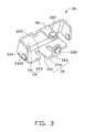
- FIG. 3is an enlarged view of an elastic member of FIG. 1 .
- FIG. 4is an assembled, schematic view of FIG. 1 .
- FIG. 5is similar to FIG. 4 , but shown from another aspect.
- FIG. 6is a cross-sectional view of FIG. 5 along VI-VI line thereof.
- the present grounding mechanismmay be applied in many different electronic devices such as mobile phones, game devices, PDAs (personal digital assistant) and others.
- the grounding mechanismis used in a mobile phone.
- the mobile phone 100includes a liquid crystal module 10 (partially shown), an elastic member 20 , a first housing 30 , and a second housing 40 .
- the liquid crystal module 10is disposed between the first housing 30 and the second housing 40 .
- the elastic member 20conducts electromagnetic charges from the liquid crystal module 10 to a ground pin of a printed circuit board (not shown) of the mobile phone 100 .
- the liquid crystal module 10includes a first conductive element 14 .
- the first conducive element 14is made of metal, and is used for transferring electromagnetic charges away from the liquid crystal module 10 .
- the elastic member 20is metal, and may be stamped or punched from a metal sheet.
- the elastic member 20includes a main base 24 .
- the main base 24includes a mounting portion 241 and a support portion 243 at an angle to the mounting portion 241 .
- Two fixing portions 242respectively perpendicularly extend from opposite sides of the mounting portion 241 .
- a protrusion 2422extends from each fixing portion 242 .
- the support portion 243defines an opening 245 .
- a resisting portion 26extends from the support portion 243 in the opening 245 configured to electrically connect to the first conductive element 14 .
- the resisting portion 26includes a holding part 262 , a connecting part 264 , and a contact part 266 .
- the holding part 262directly extends from the support portion 243 , and is coplanar with the support portion 243 .
- the connecting part 264extends from the holding part 262 and is at an approximately obtuse angle to the holding part 262 .
- the contact part 266is inclined to the connecting part 264 , and is opposite to the mounting portion 241 .
- a substantially hemispherical first projection 268is formed at the contact part 266 .
- a latching portion 28extends from the mounting portion 241 opposite to the support portion 243 .
- a substantially hemispherical second projection 282is formed at the latching portion 28 .
- the first housing 30includes a sidewall 31 and a second conductive element 33 .
- the second conductive element 33is integrally formed with the first housing 30 by insert molding process.
- the first housing 30includes a receiving portion 32 adjacent to the sidewall 31 for receiving the elastic member 20 .
- the receiving portion 32includes two spaced L-shape stopper plates 34 .
- One end of each stopper plate 34is integrally formed with the sidewall 31 .
- a gap 38is defined between the other ends of the stopper plates 34 .
- the stopper plates 34 and the sidewall 31cooperatively define a receiving groove 36 .
- the elastic member 20is configured to be engaged in the receiving groove 36 .
- One portion of the second conductive element 33is exposed from the receiving groove 36 .
- the second housing 40is configured to be detachably attached to the first housing 30 for clamping the liquid crystal module 10 within.
- the second housing 40includes a rib 42 configured for abutting against the elastic member 20 .
- the elastic member 20is inserted into the receiving groove 36 .
- the mounting portion 241contacts the sidewall 31 .
- the fixing portions 242respectively abut the stopper plates 34 .
- the protrusions 2422respectively elastically resist the stopper plates 34 .
- the elastic member 20is engaged in the receiving portion 32 .
- the second projection 282 of the latching portion 28is electrically connected to the second conductive element 33 .
- the resisting portion 26is exposed from the receiving groove 36 , and is inserted into the gap 38 .
- the contact part 266is exposed from the gap 38 .
- the liquid crystal module 10is attached to the first housing 30 .
- the first projection 268is electrically connected to the first conductive element 14 .
- the second housing 40is attached to the liquid crystal module 10 .
- the rib 42elastically resists the support portion 243 and the holding part 262 . Therefore, the first conductive element 14 , the elastic member 20 , and the second conductive element 33 are electronically connected to a grounding pin of the printed circuit board.
- a significant advantage of the grounding mechanismis that the elastic member 20 is easily assembled to the mobile phone 100 . This simplifies assembly of the electronic device so that costs are reduced.
- the first projection 268 and the second projection 282may provide a more stable connection.
Landscapes
- Physics & Mathematics (AREA)
- Nonlinear Science (AREA)
- Mathematical Physics (AREA)
- Chemical & Material Sciences (AREA)
- Crystallography & Structural Chemistry (AREA)
- General Physics & Mathematics (AREA)
- Optics & Photonics (AREA)
- Liquid Crystal (AREA)
- Devices For Indicating Variable Information By Combining Individual Elements (AREA)
- Elimination Of Static Electricity (AREA)
Abstract
Description
Claims (8)
Applications Claiming Priority (3)
| Application Number | Priority Date | Filing Date | Title |
|---|---|---|---|
| CN200910307788 | 2009-09-25 | ||
| CN200910307788.X | 2009-09-25 | ||
| CN200910307788XACN102036459A (en) | 2009-09-25 | 2009-09-25 | Grounding device and portable electronic device applying same |
Publications (2)
| Publication Number | Publication Date |
|---|---|
| US20110075064A1 US20110075064A1 (en) | 2011-03-31 |
| US8368835B2true US8368835B2 (en) | 2013-02-05 |
Family
ID=43779980
Family Applications (1)
| Application Number | Title | Priority Date | Filing Date |
|---|---|---|---|
| US12/771,274Expired - Fee RelatedUS8368835B2 (en) | 2009-09-25 | 2010-04-30 | Grounding mechanism for liquid crystal module |
Country Status (2)
| Country | Link |
|---|---|
| US (1) | US8368835B2 (en) |
| CN (1) | CN102036459A (en) |
Families Citing this family (4)
| Publication number | Priority date | Publication date | Assignee | Title |
|---|---|---|---|---|
| CN102036459A (en)* | 2009-09-25 | 2011-04-27 | 深圳富泰宏精密工业有限公司 | Grounding device and portable electronic device applying same |
| CN105202419B (en)* | 2015-10-08 | 2018-02-06 | 京东方科技集团股份有限公司 | A kind of backlight and display device |
| CN105636383A (en)* | 2016-03-11 | 2016-06-01 | 珠海格力电器股份有限公司 | Electronic equipment and shell structure thereof |
| CN107394426A (en)* | 2017-06-22 | 2017-11-24 | 上海斐讯数据通信技术有限公司 | A kind of grounding elastic part and the structure using the grounding elastic part |
Citations (16)
| Publication number | Priority date | Publication date | Assignee | Title |
|---|---|---|---|---|
| US5719739A (en)* | 1994-01-13 | 1998-02-17 | Horiguchi; Noboru | Static eliminator |
| US6028761A (en)* | 1997-03-04 | 2000-02-22 | C-Technologies Llc | Apparatus and method for monitoring, controlling, displaying and dissipating an electrostatic charge |
| US6122704A (en)* | 1989-05-15 | 2000-09-19 | Dallas Semiconductor Corp. | Integrated circuit for identifying an item via a serial port |
| US20020185659A1 (en)* | 2001-04-04 | 2002-12-12 | Shuichiro Yamaguchi | Non-reciprocal circuit device |
| US20040106428A1 (en)* | 2002-11-19 | 2004-06-03 | Hideaki Shoji | Portable wireless communication apparatus |
| US20050024500A1 (en)* | 2003-07-31 | 2005-02-03 | Kyocera Corporation | Camera device, electronic device, and image processing method for same |
| US20050109669A1 (en)* | 2003-11-07 | 2005-05-26 | John Burns | Substrate container |
| US20050139003A1 (en)* | 2003-02-26 | 2005-06-30 | Rudolph Bergsma Trust | Hermetic fuel level sender |
| US20050237275A1 (en)* | 2004-04-26 | 2005-10-27 | Hirokazu Inoue | Plasma display apparatus |
| US20060040520A1 (en)* | 2004-08-19 | 2006-02-23 | Samsung Electronics Co., Ltd. | Flat panel display device including a conductive compressible body |
| US7121889B1 (en)* | 2005-05-11 | 2006-10-17 | Myoungsoo Jeon | High speed connector assembly with laterally displaceable head portion |
| US7121874B1 (en)* | 2005-09-26 | 2006-10-17 | Myoungsoo Jeon | Flexible printed circuit (FPC) edge connector |
| US7190053B2 (en)* | 2004-09-16 | 2007-03-13 | Rosemount Inc. | Field device incorporating circuit card assembly as environmental and EMI/RFI shield |
| US20070211711A1 (en)* | 2006-03-08 | 2007-09-13 | Clayton James E | Thin multichip flex-module |
| US20090154050A1 (en)* | 2004-06-30 | 2009-06-18 | Research In Motion Limited | Spark gap apparatus and method for electrostatic discharge protection |
| US20110075064A1 (en)* | 2009-09-25 | 2011-03-31 | Shenzhen Futaihong Precision Industry Co., Ltd. | Grounding mechanism for liquid crystal module |
Family Cites Families (4)
| Publication number | Priority date | Publication date | Assignee | Title |
|---|---|---|---|---|
| CN101359779B (en)* | 2007-08-03 | 2011-03-23 | 深圳富泰宏精密工业有限公司 | Earthing device of portable electronic apparatus |
| CN101378155B (en)* | 2007-08-28 | 2011-07-27 | 深圳富泰宏精密工业有限公司 | Grounding device and portable electronic device containing the same |
| CN101425631B (en)* | 2007-10-31 | 2011-07-27 | 深圳富泰宏精密工业有限公司 | Spring leaf construction and array type spring leaf device applying the construction |
| CN101472378B (en)* | 2007-12-28 | 2011-12-21 | 深圳富泰宏精密工业有限公司 | Shrapnel structure and electronic device applying the same |
- 2009
- 2009-09-25CNCN200910307788XApatent/CN102036459A/enactivePending
- 2010
- 2010-04-30USUS12/771,274patent/US8368835B2/ennot_activeExpired - Fee Related
Patent Citations (19)
| Publication number | Priority date | Publication date | Assignee | Title |
|---|---|---|---|---|
| US6122704A (en)* | 1989-05-15 | 2000-09-19 | Dallas Semiconductor Corp. | Integrated circuit for identifying an item via a serial port |
| US5719739A (en)* | 1994-01-13 | 1998-02-17 | Horiguchi; Noboru | Static eliminator |
| US6028761A (en)* | 1997-03-04 | 2000-02-22 | C-Technologies Llc | Apparatus and method for monitoring, controlling, displaying and dissipating an electrostatic charge |
| US20020185659A1 (en)* | 2001-04-04 | 2002-12-12 | Shuichiro Yamaguchi | Non-reciprocal circuit device |
| US6765453B2 (en)* | 2001-04-04 | 2004-07-20 | Matsushita Electric Industrial Co., Ltd. | Non-reciprocal circuit device having a thermal conductor |
| US20040106428A1 (en)* | 2002-11-19 | 2004-06-03 | Hideaki Shoji | Portable wireless communication apparatus |
| US7184808B2 (en)* | 2002-11-19 | 2007-02-27 | Sony Ericsson Mobile Communication Japan, Inc. | Portable wireless communication apparatus |
| US20050139003A1 (en)* | 2003-02-26 | 2005-06-30 | Rudolph Bergsma Trust | Hermetic fuel level sender |
| US20050024500A1 (en)* | 2003-07-31 | 2005-02-03 | Kyocera Corporation | Camera device, electronic device, and image processing method for same |
| US20050109669A1 (en)* | 2003-11-07 | 2005-05-26 | John Burns | Substrate container |
| US20050237275A1 (en)* | 2004-04-26 | 2005-10-27 | Hirokazu Inoue | Plasma display apparatus |
| US7557776B2 (en)* | 2004-04-26 | 2009-07-07 | Hitachi, Ltd. | Plasma display apparatus |
| US20090154050A1 (en)* | 2004-06-30 | 2009-06-18 | Research In Motion Limited | Spark gap apparatus and method for electrostatic discharge protection |
| US20060040520A1 (en)* | 2004-08-19 | 2006-02-23 | Samsung Electronics Co., Ltd. | Flat panel display device including a conductive compressible body |
| US7190053B2 (en)* | 2004-09-16 | 2007-03-13 | Rosemount Inc. | Field device incorporating circuit card assembly as environmental and EMI/RFI shield |
| US7121889B1 (en)* | 2005-05-11 | 2006-10-17 | Myoungsoo Jeon | High speed connector assembly with laterally displaceable head portion |
| US7121874B1 (en)* | 2005-09-26 | 2006-10-17 | Myoungsoo Jeon | Flexible printed circuit (FPC) edge connector |
| US20070211711A1 (en)* | 2006-03-08 | 2007-09-13 | Clayton James E | Thin multichip flex-module |
| US20110075064A1 (en)* | 2009-09-25 | 2011-03-31 | Shenzhen Futaihong Precision Industry Co., Ltd. | Grounding mechanism for liquid crystal module |
Also Published As
| Publication number | Publication date |
|---|---|
| CN102036459A (en) | 2011-04-27 |
| US20110075064A1 (en) | 2011-03-31 |
Similar Documents
| Publication | Publication Date | Title |
|---|---|---|
| US7586753B2 (en) | Portable electronic device with single printed circuit board | |
| US7576291B2 (en) | Key button mechanism and an electronic device using the same | |
| US7654829B1 (en) | Electronic device and connector assembly | |
| US7306491B1 (en) | Chip card retaining mechanism and electronic device therewith | |
| US7402082B2 (en) | Electrical connector with retaining shell | |
| US7819696B2 (en) | Shielded connector having prolonged latches to provide reliable retaining force to positioning the camera module mounted therein | |
| US8548189B2 (en) | Positioning structure for speaker of portable electronic device | |
| CN1183470C (en) | A subscriber identity module card holder | |
| US8100719B2 (en) | Electronic device with grounding mechanism | |
| US8248808B2 (en) | Portable electronic device with clip mechanism | |
| US7682166B2 (en) | Electronic device with grounding mechanism | |
| US8367930B2 (en) | Grounding mechanism for electronic device | |
| US8368835B2 (en) | Grounding mechanism for liquid crystal module | |
| US20100033939A1 (en) | Earpiece fixing structure and electronic device using the same | |
| JP2005166286A (en) | Card holding structure of portable electronic apparatus | |
| US20070131777A1 (en) | Chip card retaining mechanism | |
| US8746573B2 (en) | Smart card holding member and portable electronic device employing the same | |
| US7988490B2 (en) | Retaining clip for connector | |
| US7252529B2 (en) | Chip card retaining mechanism | |
| US7985107B2 (en) | Battery connector and portable electronic device using same | |
| US8391024B2 (en) | Electronic device with card connection mechanism | |
| KR20150096986A (en) | Clip type contact terminal on the board | |
| CN105720435B (en) | Electronic device | |
| US8100714B2 (en) | Connector and electronic device using same | |
| US8223502B2 (en) | Chip card holder and electronic device using the same |
Legal Events
| Date | Code | Title | Description |
|---|---|---|---|
| AS | Assignment | Owner name:FIH (HONG KONG) LIMITED, HONG KONG Free format text:ASSIGNMENT OF ASSIGNORS INTEREST;ASSIGNOR:OUYANG, ZHI-BIN;REEL/FRAME:024318/0022 Effective date:20100426 Owner name:SHENZHEN FUTAIHONG PRECISION INDUSTRY CO., LTD., C Free format text:ASSIGNMENT OF ASSIGNORS INTEREST;ASSIGNOR:OUYANG, ZHI-BIN;REEL/FRAME:024318/0022 Effective date:20100426 | |
| STCF | Information on status: patent grant | Free format text:PATENTED CASE | |
| FPAY | Fee payment | Year of fee payment:4 | |
| FEPP | Fee payment procedure | Free format text:MAINTENANCE FEE REMINDER MAILED (ORIGINAL EVENT CODE: REM.); ENTITY STATUS OF PATENT OWNER: LARGE ENTITY | |
| LAPS | Lapse for failure to pay maintenance fees | Free format text:PATENT EXPIRED FOR FAILURE TO PAY MAINTENANCE FEES (ORIGINAL EVENT CODE: EXP.); ENTITY STATUS OF PATENT OWNER: LARGE ENTITY | |
| STCH | Information on status: patent discontinuation | Free format text:PATENT EXPIRED DUE TO NONPAYMENT OF MAINTENANCE FEES UNDER 37 CFR 1.362 | |
| FP | Lapsed due to failure to pay maintenance fee | Effective date:20210205 |