US8368448B2 - Delay lines, methods for delaying a signal, and delay lock loops - Google Patents
Delay lines, methods for delaying a signal, and delay lock loopsDownload PDFInfo
- Publication number
- US8368448B2 US8368448B2US13/426,402US201213426402AUS8368448B2US 8368448 B2US8368448 B2US 8368448B2US 201213426402 AUS201213426402 AUS 201213426402AUS 8368448 B2US8368448 B2US 8368448B2
- Authority
- US
- United States
- Prior art keywords
- delay
- input
- coupled
- signal
- clock signal
- Prior art date
- Legal status (The legal status is an assumption and is not a legal conclusion. Google has not performed a legal analysis and makes no representation as to the accuracy of the status listed.)
- Active
Links
- 230000003111delayed effectEffects0.000claimsabstractdescription26
- 230000000295complement effectEffects0.000claimsdescription7
- VUKDZGAUWUDQRZ-XKLVTHTNSA-N[[(2r,3s,4r,5r)-5-(6-aminopurin-9-yl)-3,4-dihydroxyoxolan-2-yl]methoxy-hydroxyphosphoryl] 2-phenylacetateChemical compoundC([C@H]1O[C@H]([C@@H]([C@@H]1O)O)N1C=2N=CN=C(C=2N=C1)N)OP(O)(=O)OC(=O)CC1=CC=CC=C1VUKDZGAUWUDQRZ-XKLVTHTNSA-N0.000description31
- 230000007704transitionEffects0.000description14
- 230000000630rising effectEffects0.000description5
- 238000010586diagramMethods0.000description4
- 230000008878couplingEffects0.000description2
- 238000010168coupling processMethods0.000description2
- 238000005859coupling reactionMethods0.000description2
- 230000001934delayEffects0.000description2
- 230000010363phase shiftEffects0.000description2
- 230000001360synchronised effectEffects0.000description2
- 238000011144upstream manufacturingMethods0.000description2
- 230000002411adverseEffects0.000description1
- 230000008901benefitEffects0.000description1
- 230000003247decreasing effectEffects0.000description1
- 238000012886linear functionMethods0.000description1
- 230000004048modificationEffects0.000description1
- 238000012986modificationMethods0.000description1
- 230000000644propagated effectEffects0.000description1
- 230000004044responseEffects0.000description1
Images


Classifications
- H—ELECTRICITY
- H03—ELECTRONIC CIRCUITRY
- H03L—AUTOMATIC CONTROL, STARTING, SYNCHRONISATION OR STABILISATION OF GENERATORS OF ELECTRONIC OSCILLATIONS OR PULSES
- H03L7/00—Automatic control of frequency or phase; Synchronisation
- H03L7/06—Automatic control of frequency or phase; Synchronisation using a reference signal applied to a frequency- or phase-locked loop
- H03L7/08—Details of the phase-locked loop
- H03L7/081—Details of the phase-locked loop provided with an additional controlled phase shifter
- H03L7/0812—Details of the phase-locked loop provided with an additional controlled phase shifter and where no voltage or current controlled oscillator is used
- H03L7/0816—Details of the phase-locked loop provided with an additional controlled phase shifter and where no voltage or current controlled oscillator is used the controlled phase shifter and the frequency- or phase-detection arrangement being connected to a common input
- H—ELECTRICITY
- H03—ELECTRONIC CIRCUITRY
- H03K—PULSE TECHNIQUE
- H03K5/00—Manipulating of pulses not covered by one of the other main groups of this subclass
- H03K5/13—Arrangements having a single output and transforming input signals into pulses delivered at desired time intervals
- H03K5/133—Arrangements having a single output and transforming input signals into pulses delivered at desired time intervals using a chain of active delay devices
- H—ELECTRICITY
- H03—ELECTRONIC CIRCUITRY
- H03K—PULSE TECHNIQUE
- H03K5/00—Manipulating of pulses not covered by one of the other main groups of this subclass
- H03K5/13—Arrangements having a single output and transforming input signals into pulses delivered at desired time intervals
- H03K5/14—Arrangements having a single output and transforming input signals into pulses delivered at desired time intervals by the use of delay lines
- H—ELECTRICITY
- H03—ELECTRONIC CIRCUITRY
- H03L—AUTOMATIC CONTROL, STARTING, SYNCHRONISATION OR STABILISATION OF GENERATORS OF ELECTRONIC OSCILLATIONS OR PULSES
- H03L7/00—Automatic control of frequency or phase; Synchronisation
- H03L7/06—Automatic control of frequency or phase; Synchronisation using a reference signal applied to a frequency- or phase-locked loop
- H03L7/08—Details of the phase-locked loop
- H03L7/081—Details of the phase-locked loop provided with an additional controlled phase shifter
- H03L7/0812—Details of the phase-locked loop provided with an additional controlled phase shifter and where no voltage or current controlled oscillator is used
- H03L7/0814—Details of the phase-locked loop provided with an additional controlled phase shifter and where no voltage or current controlled oscillator is used the phase shifting device being digitally controlled
- H—ELECTRICITY
- H03—ELECTRONIC CIRCUITRY
- H03L—AUTOMATIC CONTROL, STARTING, SYNCHRONISATION OR STABILISATION OF GENERATORS OF ELECTRONIC OSCILLATIONS OR PULSES
- H03L7/00—Automatic control of frequency or phase; Synchronisation
- H03L7/06—Automatic control of frequency or phase; Synchronisation using a reference signal applied to a frequency- or phase-locked loop
- H03L7/08—Details of the phase-locked loop
- H03L7/081—Details of the phase-locked loop provided with an additional controlled phase shifter
- H03L7/0812—Details of the phase-locked loop provided with an additional controlled phase shifter and where no voltage or current controlled oscillator is used
- H03L7/0818—Details of the phase-locked loop provided with an additional controlled phase shifter and where no voltage or current controlled oscillator is used the controlled phase shifter comprising coarse and fine delay or phase-shifting means
- H—ELECTRICITY
- H03—ELECTRONIC CIRCUITRY
- H03L—AUTOMATIC CONTROL, STARTING, SYNCHRONISATION OR STABILISATION OF GENERATORS OF ELECTRONIC OSCILLATIONS OR PULSES
- H03L7/00—Automatic control of frequency or phase; Synchronisation
- H03L7/06—Automatic control of frequency or phase; Synchronisation using a reference signal applied to a frequency- or phase-locked loop
- H03L7/08—Details of the phase-locked loop
- H03L7/085—Details of the phase-locked loop concerning mainly the frequency- or phase-detection arrangement including the filtering or amplification of its output signal
- H03L7/089—Details of the phase-locked loop concerning mainly the frequency- or phase-detection arrangement including the filtering or amplification of its output signal the phase or frequency detector generating up-down pulses
Definitions
- This inventionrelates to delay lines and delay lock loops using delay lines, and, more particularly, in one or more embodiments, to a delay line providing improved linearity and duty cycle symmetry.
- the DLL 10includes a delay line 14 , which, as explained in greater detail below, includes a large number of gates coupled to each other in series.
- the delay line 14receives a reference clock signal CLK REF and generates an output clock signal CLK OUT having a delay relative to the reference clock signal CLK REF that is controlled by a delay control signal DelCtrl.
- the delay control signal DelCtrladjusts the delay provided by the delay line 14 by altering the number of gates through which the CLK REF is coupled.
- the DLL 10also includes a phase detector 16 and delay controller 18 coupled to outputs of the phase detector 16 for adjusting the delay of the delay line 14 .
- the phase detector 16compares the phase of the reference clock signal CLK REF to the phase of an output clock signal CLK OUT generated by delay line 14 to determine a phase error.
- the CLK OUT signalis thus used as a feedback clock signal, although other signals derived from the CLK OUT signal may instead be used as the feedback clock signal.
- the feedback clock signalis coupled to the input of phase detector though a model delay circuit 20 .
- the model delay circuit 20delays the feedback clock signal by substantially the sum of the input delay of the CLK REF signal being coupled to the phase detector 16 and the output delay of the CLK OUT signal being coupled from the delay line 14 .
- the phase of the CLK OUT signalis accurately synchronized to the phase of the CLK REF signal.
- the phase detector 16is a digital phase detector, it typically generates an UP signal if the CLK OUT signal leads the CLK REF signal by more than a first phase error.
- the delay controller 18responds to the UP signal by increasing the delay of the delay line 14 to reduce the phase error.
- the phase detector 16generates a DN signal if the CLK OUT signal lags the CLK REF signal by more than a second phase error. In that case, the delay controller 18 responds to the DN signal by decreasing the delay of the delay line 14 to again reduce the phase error.
- the phase detector 16generates neither an UP signal nor a DN signal if the magnitude of the phase error is between the first phase error and the second phase error.
- the DLL 10can be used for a variety of functions in a memory device and in other integrated circuit devices.
- the DLL 10can be used in a memory device to perform such functions as synchronizing one signal, such as a data strobe signal DQS, to another signal, such as an external clock signal as long as a delay in coupling the external clock signal to the DLL 10 and a delay in coupling the DQS signal from the DLL 10 are compensated for by corresponding model delays in the feedback path of the DLL 10 .
- the DQS signalcan then be used to latch data at a time that is synchronized with the external clock signal.
- the degree to which the DLL 10 is able to lock the phase of the CLK OUT signal to the phase of the CLK REF signalis largely determined by the delay adjustability of the delay line 14 . If the delay of the delay line 14 can only be adjusted in relatively coarse steps, the error between the phase of the CLK OUT signal and the phase of the CLK REF signal can be relatively large. For this reason, it is desirable for the delay line 14 to have a large number of gates or other delay devices. A large number of gates or other delay devices allows the delay of the delay line to be adjusted in a larger number of steps.
- the delay line 14can adjust the delay of the delay line in approximately 5 degree steps (i.e., (360° minus delay of model delay circuits)/72).
- a large number of gates or other delay devicesprovides a great deal of delay adjustability, it can also result in a large power consumption.
- a phase mixer(not shown) can be used to interpolate between relatively coarse steps.
- the CLK OUT signalis delayed relative to the CLK REF signal by the sum of the coarse steps provided by the delay line and fine steps provided by the phase mixer.
- the minimum step sizeis then the size of a fine step.
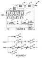
- FIG. 1is a block diagram of a conventional delay lock loop using a delay line to delay a reference clock signal.
- FIG. 2is a block diagram of a conventional delay lock loop using a delay line in combination with a phase mixer to delay a reference clock signal.
- FIG. 3is a block diagram of a delay lock loop using a delay line in combination with a phase mixer according to one embodiment of the invention.
- FIG. 4is a logic diagram of an embodiment of a phase inverter that may be used in the delay lock loop of FIG. 3 or in some other delay lock loop.
- a typical prior art DLL 30 using a delay line in combination with a phase mixeris shown in FIG. 2 .
- the DLL 30may include the same phase detector 16 and model delay 20 used in the DLL 10 of FIG. 1 .
- a delay line 50 included in the DLL 30includes a plurality of delay stages 54 a - d that are coupled to each other in series.
- the first delay stage 54 areceives the CLK REF signal.
- Each of the delay stages 54 a - dincludes a pair of series-coupled NAND gates 56 , 58 and an exit NAND gate 60 .
- the NAND gates 56 , 58are enabled by respective EnNx signals applied to the respective delay stages 54 .
- each delay stage 54couples a clock signal applied to the input of the delay stage 54 to the output of the delay stage.
- Each of the delay stages 54 in the delay line 50also receives a respective exit control signal ExitEnx, which enables the respective exit NAND gate 60 so that the gate 60 can couple a received clock signal to an input of an exit tree 70 .
- the exit tree 70includes a pair of NAND gates 74 , 76 coupled to the exit NAND gates 60 of the delay line as shown.
- the exit tree 70applies two clock signals EvenOut and OddOut, which are delayed from each other by the delay of the two NAND gates 56 , 58 , to an input of a phase mixer 80 .
- the phase mixer 80generates a feedback clock signal CLK FB with a phase that is interpolated between the delay between the EvenOut and OddOut signals.
- CLK FB signalis applied to one of the inputs of the phase detector 16 .
- the phase detector 16responds to a comparison between the phase of the CLK REF signal and the CLK FB signal by selectively generating UP and DN signals.
- a delay controller 84includes conventional logic used to generate delay control signals, such as EnNx signals, ExitEnx signals, and an INTER signal.
- delay controller 84could generate high EnNx signals that are applied to the NAND gates 56 , 58 in a delay stage 54 selected in response to the UP and DN signals.
- the delay controller 84also applies high EnNx signals to the respective NAND gates 56 , 58 in all of the delay stages 54 upstream from the selected delay stage 54 and low EnNx signals to the respective NAND gates 56 , 58 in all of the delay stages 54 downstream from the selected delay stage 54 .
- the CLK REF signalis coupled through the selected delay stage 54 and all of the delay stages 54 upstream from the selected delay stage 54 .
- the CLK REF signalis not coupled through the delay stages 54 downstream from the selected delay stage 54 because the low EnNx signals applied to these stages disable the NAND gates 56 , 58 in those stages, thereby avoiding power being wasted in these stages.
- the delay controller 84also applies a high ExitEnx signal to exit NAND gate 60 in the selected delay stage 54 , and it applies respective low ExitENx signals to the exit NAND gate 60 in each of the other delay stages 54 .
- the low ExitEnx signal applied to the NAND gate 60 in each of the remaining stagescauses the NAND gate 60 to output a high, which enables the NAND gates 74 , 76 in the exit tree 70 so that the selected delay stage 54 can couple its input and output through the NAND gates 74 , 76 .
- the delay controller 84selects one of the delay stages 54 in the delay line 50 .
- the delay controller 84also generates an INTER value that causes the phase mixer 80 to interpolate between the EvenOut and OddOut signals to minimize the phase error determined by the phase detector 16 . Therefore, the delay line 50 is used to apply a coarse adjustment to the delay of the CLK FB signal, and the phase mixer 80 is used to interpolate within the coarse delay to apply a fine adjustment to the phase of the CLK OUT signal.
- the DLL 30 shown in FIG. 3performs well in a variety of conventional applications, but nevertheless exhibits a variety of undesirable traits and limitations.
- the problems with conventional DLLs, such as the DLL 30are due primarily to the fact that each delay stage in the delay line 50 has two inverting gates 56 , 58 to ensure good duty cycle control. In most inverting delay circuits, the transition from a first logic level to a second logic level is faster than the transition from the second logic level back to the first logic level.
- the NAND gatemight have different rise and fall times than the inverter, which would be accumulated from all of the delay stages, thereby resulting in duty cycle error, which would result in the CLK FB signal not having a 50% duty cycle.
- a deviation from a duty cycle of 50%can be particularly problematic for many applications.
- a DQS signalis used in current memory devices to latch data on both the rising edge and the falling edge of the DQS signal.
- the CLK OUT signaldoes not have a 50% duty cycle and it is used to generate the DQS signal, the rising and falling edges of the DQS signal will generally not occur at the center of the period during which the data to be latched are valid. Such skews that can occur in the timing of the DQS signal relative to the data can thus prevent the proper data from being latched.
- the uses of two NAND gates 56 , 58 in each stage 54 of the delay line 50avoids the problem of duty cycle skew because the signal applied to every stage always transitions both high and low on each transition of the signal before the signal is propagated to the output of that stage.
- the phase detector 16 shown in FIG. 2has characteristics that limit the performance of the DLL 30 .
- Second, two NAND gates 56 , 58 or other inverting delay devices for each stageprovide a relatively large delay which can adversely affect the ability of the phase mixer 80 to linearity adjust the delay of the delay line 50 .
- the delay provided by the phase mixer 80should be a linear function of the value of an interpolation signal so that the sizes of all of the fine steps are equal to each other.
- the non-linearity of a phase mixeris normally a fixed percentage of the range over which the phase mixer interpolates, the larger coarse step required to cover two NAND gates 56 , 58 or other inverting delay devices results in a greater degree of non-linearity.
- a DLL 100 using a delay line 120 in combination with a phase mixer 110 according to an embodiment of the inventionis shown in FIG. 3 .
- the DLL 100may use the same delay controller 84 used in the DLL 30 , and it may provide the same EnNx and ExitEnx signals.
- DLL 100may use the same exit tree 70 used in the DLL 30 , and it may receive the same ExitEnx signals and output the EvenOut and OddOut* signals. Therefore, an explanation of the structure and operation of the delay controller 84 and the exit tree 70 will not be repeated.
- the DLL 100differs from the DLL 30 by using a delay line 120 that is different from the delay line 50 used in the DLL 30 , and it uses a phase inverter 130 , which is not used in the DLL 30 .
- a DLL according to other embodiments of the inventionmay have other differences from the DLL 30 .
- the delay line 120includes a plurality of delay stages 124 , each of which includes only a single NAND gate 126 , although other embodiments may use other inverting delay (e.g., logic) devices such as NOR gates and inverters, to name two such delay devices.
- the size of the coarse step over which the delay of the delay line 120 is adjustedmay be approximately half the size of the coarse step of the delay line 50 used in the prior art DLL 30 .
- the output from each delay stage 124 of the delay line 120is the delayed complement of the phase of the input to that delay stage 124 .
- the coarse step of the delay line 120is the difference between the phase shift through the NAND gate 126 and 180 degrees.
- this coarse stepwould normally be significantly larger than the size of the coarse step provided by the delay line 50 , and would thus defeat the major advantage to using a single NAND gate 126 or other inverting delay device for each stage rather than two NAND gates 56 , 58 for each stage 54 as used in the delay line 50 .
- the 180 degree phase shiftcould, of course, be eliminated by using a non-inverting delay device in each stage. But doing so would cause the delay devices in each of the delay stages to transition in the same direction. As a result, any difference in the time to transition between logic levels in opposite directions in each delay stage would be magnified by the number of delay stages in the delay line 120 , which might result in the delay line creating substantial duty cycle skew.
- a rising edge transition of an input signal applied to a delay line 120 containing only non-inverting delay deviceswould result in all of the delay devices transitioning from high-to-low.
- the non-inverting delay deviceswould all transition from low-to-high. If the low-to-high transition required more time than the high-to-low transition, the duty cycle of the input signal would be skewed by all of the delay devices, thus resulting in a significant deviation from a 50% duty cycle.
- the DLL 100allows use of the delay line 120 with a single inverting delay device in each stage by using the delay line 120 in combination with the phase inverter 130 .
- the phase inverter 130passes the EvenOut signal without inverting it and inverts the OddOut* signal to provide an OddOut signal that is no longer the complement of the EvenOut signal.
- the phase inverter 130can have the same propagation delay for both the EvenOut signal and the OddOut signal so that the phase of the EvenOut signal differs from the phase of OddOut signal by only the propagation delay though one of the NAND gates 126 .
- the size of the coarse delay over which the phase mixer 110 is only approximately half the size of the coarse step over the phase mixer 80 used in the DLL 30must interpolate. Therefore, the linearity of the phase mixer 110 used in the DLL 100 should be significantly improved.
- the delay line 120 used in the DLL 100does invert the CLK REF signal over an odd number of delay stages 124 to provide either the EvenOut signal or the OddOut* signal.
- the mismatch between the number of rising edge transitions of the CLR REF signal compared to the number of falling edge transitions of the CLK REFis a single leading edge or rising edge transition. Therefore, for example, if there are 72 delay stages 124 , the CLK REF may have a duty cycle that deviates from 50% only to the extent of a disparity in the rise time and fall time of a single delay stage 124 .
- a phase inverter 130according to one embodiment of the invention is shown in FIG. 4 .
- the phase inverter 130includes a pair of series coupled inverters 140 , 142 , the first of which 140 receives the EvenOut signal and the last of which generates one of the signals applied to the phase mixer.
- the OddOut signalis applied to the first of a series of three inverters 150 , 152 , 154 .
- the final inverter 154has its output coupled to the other input of the phase mixer 110 ( FIG. 3 ). Insofar as the OddOut signal is the complement of the EvenOut signal, the signals output from the phase inverter 130 have the same phase in the same manner that the phase mixer receives signals having the same phase in the prior art circuit shown in FIG. 1 .
- the OddOut signalwould be delayed relative to the EvenOut signal by more than the delay of one delay stage because the OddOut signal is inverted by three inverters 150 , 152 , 154 while the EvenOut signal is inverted by only two inverters 140 , 142 .
- transistors (not shown) in the inverters 140 , 142 , 150 , 152 , 154are fabricated with a size that causes the collective delay of the two inverters 140 , 142 to be equal to the collective delay of the three inverters 150 , 152 , 154 .
- the transistors in the inverter 140have different electrical characteristics from the transistors in the inverter 150 , and they would therefore load the respective signal lines coupled to their inputs to different degrees.
- an impedance compensating devicesuch as an extra inverter 160 having the same electrical characteristics as the inverter 150 , is connected to the input of the inverter 140 .
- an extra inverter 164 having the same electrical characteristics as the inverter 140is connected to the input of the inverter 150 .
- both inputs to the phase inverter 130have the same input impedance.
- the extra inverters 160 , 164are not used.
- other embodiments of the phase inverter 130may use different designs.
- the delay controller 84includes conventional logic that selectively applies EnNx signals to the NAND gates 56 , 58 in each delay stage 54 to disable the delay stages 54 downstream from a selected delay stage.
- the gates 56 , 58 in all of the delay stages 54my be permanently enabled, particularly if power consumption is not an issue. In such cases, rather than using a permanently enabled gate, inverters may be used in place of gates. Such modifications are well within the skill of those ordinarily skilled in the art. Accordingly, the invention is not limited except as by the appended claims.
Landscapes
- Physics & Mathematics (AREA)
- Nonlinear Science (AREA)
- Pulse Circuits (AREA)
Abstract
Description
Claims (20)
Priority Applications (3)
| Application Number | Priority Date | Filing Date | Title |
|---|---|---|---|
| US13/426,402US8368448B2 (en) | 2009-01-21 | 2012-03-21 | Delay lines, methods for delaying a signal, and delay lock loops |
| US13/734,745US8502579B2 (en) | 2009-01-21 | 2013-01-04 | Delay lines, methods for delaying a signal, and delay lock loops |
| US13/957,333US8624644B2 (en) | 2009-01-21 | 2013-08-01 | Devices including phase inverters and phase mixers |
Applications Claiming Priority (3)
| Application Number | Priority Date | Filing Date | Title |
|---|---|---|---|
| US12/356,916US7872507B2 (en) | 2009-01-21 | 2009-01-21 | Delay lines, methods for delaying a signal, and delay lock loops |
| US12/986,973US8149034B2 (en) | 2009-01-21 | 2011-01-07 | Delay lines, methods for delaying a signal, and delay lock loops |
| US13/426,402US8368448B2 (en) | 2009-01-21 | 2012-03-21 | Delay lines, methods for delaying a signal, and delay lock loops |
Related Parent Applications (1)
| Application Number | Title | Priority Date | Filing Date |
|---|---|---|---|
| US12/986,973DivisionUS8149034B2 (en) | 2009-01-21 | 2011-01-07 | Delay lines, methods for delaying a signal, and delay lock loops |
Related Child Applications (1)
| Application Number | Title | Priority Date | Filing Date |
|---|---|---|---|
| US13/734,745DivisionUS8502579B2 (en) | 2009-01-21 | 2013-01-04 | Delay lines, methods for delaying a signal, and delay lock loops |
Publications (2)
| Publication Number | Publication Date |
|---|---|
| US20120223755A1 US20120223755A1 (en) | 2012-09-06 |
| US8368448B2true US8368448B2 (en) | 2013-02-05 |
Family
ID=42336458
Family Applications (5)
| Application Number | Title | Priority Date | Filing Date |
|---|---|---|---|
| US12/356,916ActiveUS7872507B2 (en) | 2009-01-21 | 2009-01-21 | Delay lines, methods for delaying a signal, and delay lock loops |
| US12/986,973ActiveUS8149034B2 (en) | 2009-01-21 | 2011-01-07 | Delay lines, methods for delaying a signal, and delay lock loops |
| US13/426,402ActiveUS8368448B2 (en) | 2009-01-21 | 2012-03-21 | Delay lines, methods for delaying a signal, and delay lock loops |
| US13/734,745ActiveUS8502579B2 (en) | 2009-01-21 | 2013-01-04 | Delay lines, methods for delaying a signal, and delay lock loops |
| US13/957,333ActiveUS8624644B2 (en) | 2009-01-21 | 2013-08-01 | Devices including phase inverters and phase mixers |
Family Applications Before (2)
| Application Number | Title | Priority Date | Filing Date |
|---|---|---|---|
| US12/356,916ActiveUS7872507B2 (en) | 2009-01-21 | 2009-01-21 | Delay lines, methods for delaying a signal, and delay lock loops |
| US12/986,973ActiveUS8149034B2 (en) | 2009-01-21 | 2011-01-07 | Delay lines, methods for delaying a signal, and delay lock loops |
Family Applications After (2)
| Application Number | Title | Priority Date | Filing Date |
|---|---|---|---|
| US13/734,745ActiveUS8502579B2 (en) | 2009-01-21 | 2013-01-04 | Delay lines, methods for delaying a signal, and delay lock loops |
| US13/957,333ActiveUS8624644B2 (en) | 2009-01-21 | 2013-08-01 | Devices including phase inverters and phase mixers |
Country Status (1)
| Country | Link |
|---|---|
| US (5) | US7872507B2 (en) |
Cited By (1)
| Publication number | Priority date | Publication date | Assignee | Title |
|---|---|---|---|---|
| US8502579B2 (en)* | 2009-01-21 | 2013-08-06 | Micron Technology, Inc. | Delay lines, methods for delaying a signal, and delay lock loops |
Families Citing this family (18)
| Publication number | Priority date | Publication date | Assignee | Title |
|---|---|---|---|---|
| KR20100045186A (en)* | 2008-10-23 | 2010-05-03 | 삼성전자주식회사 | Wideband delay locked loop circuit |
| KR20100099545A (en)* | 2009-03-03 | 2010-09-13 | 삼성전자주식회사 | Delay locked loop and semi-conductor memory device using the same |
| WO2012082140A1 (en)* | 2010-12-17 | 2012-06-21 | Agilent Technologies, Inc. | Apparatus and method for providing timing adjustment of input signal |
| JP5799536B2 (en)* | 2011-03-17 | 2015-10-28 | 株式会社リコー | Fractional PLL circuit |
| KR20120111281A (en)* | 2011-03-31 | 2012-10-10 | 에스케이하이닉스 주식회사 | Data outputting circuit of a semiconductor apparatus |
| US8643414B1 (en)* | 2012-02-13 | 2014-02-04 | Rambus Inc. | Fast locking phase-locked loop |
| KR101982194B1 (en)* | 2012-06-20 | 2019-05-24 | 에스케이하이닉스 주식회사 | Delay control circuit and clock generating circuit including the same |
| US8917132B2 (en) | 2013-03-11 | 2014-12-23 | Micron Technology, Inc. | Apparatuses, methods, and circuits including a delay circuit |
| US8804456B1 (en)* | 2013-03-28 | 2014-08-12 | Nanya Technology Corp. | Delay locked loop (DLL) system for a memory device with wide operating frequency via a variable supply applied to a delay line |
| US8947144B2 (en) | 2013-06-18 | 2015-02-03 | Micron Technology, Inc. | Apparatuses and methods for duty cycle adjustment |
| US9503066B2 (en) | 2013-07-08 | 2016-11-22 | Micron Technology, Inc. | Apparatuses and methods for phase interpolating clock signals and for providing duty cycle corrected clock signals |
| KR102521756B1 (en) | 2016-06-22 | 2023-04-14 | 삼성전자주식회사 | Delay circuit of semiconductor memory device, semiconductor memory device and method of operating the same |
| KR102653891B1 (en)* | 2016-11-30 | 2024-04-02 | 삼성전자주식회사 | Phase interpolator for interpolating delayed clock signal and device including the same for operating data sampling by using phase interpolated clock signal |
| US10158352B2 (en)* | 2017-01-11 | 2018-12-18 | Mediatek Inc. | Delay signal generating apparatus using glitch free digitally controlled delay line and associated delay signal generating method |
| TWI670939B (en)* | 2018-12-03 | 2019-09-01 | 新唐科技股份有限公司 | Delay line circuit with calibration function and calibration method thereof |
| KR20220003712A (en) | 2020-07-02 | 2022-01-11 | 삼성전자주식회사 | Delay circuit of delay-locked loop circuit and delay-locked loop circuit |
| US11483004B2 (en)* | 2020-10-19 | 2022-10-25 | SK Hynix Inc. | Delay circuit and a delay locked loop circuit using the same |
| KR20220051497A (en)* | 2020-10-19 | 2022-04-26 | 에스케이하이닉스 주식회사 | Delay circuit and a delay locked loop circuit using the same |
Citations (32)
| Publication number | Priority date | Publication date | Assignee | Title |
|---|---|---|---|---|
| US5428309A (en)* | 1989-05-11 | 1995-06-27 | Mitsubishi Denki Kabushiki Kaisha | Delay circuit |
| US5712583A (en)* | 1995-11-13 | 1998-01-27 | International Business Machines Corporation | Clock phase alignment using frequency comparison |
| US6768361B2 (en)* | 2001-12-21 | 2004-07-27 | Hynix Semiconductor Inc. | Clock synchronization circuit |
| US20040155686A1 (en)* | 2003-01-10 | 2004-08-12 | Se-Jun Kim | Analog delay locked loop having duty cycle correction circuit |
| US20040201406A1 (en)* | 2001-08-08 | 2004-10-14 | Seong-Hoon Lee | Ring-resister controlled DLL with fine delay line and direct skew sensing detector |
| US20050285643A1 (en)* | 2003-12-11 | 2005-12-29 | Micron Technology, Inc. | Digital frequency-multiplying DLLs |
| US20060001463A1 (en)* | 2004-06-30 | 2006-01-05 | Lee Hyun-Woo | Digital delay locked loop capable of correcting duty cycle and its method |
| US7042309B2 (en)* | 2003-12-08 | 2006-05-09 | Werlatone, Inc. | Phase inverter and coupler assembly |
| US20060133557A1 (en)* | 2004-12-22 | 2006-06-22 | Freyman Ronald L | Phase interpolator having a phase jump |
| US7088159B2 (en)* | 2004-06-30 | 2006-08-08 | Hynix Semiconductor, Inc. | Register controlled delay locked loop and its control method |
| US20070030753A1 (en)* | 2005-07-21 | 2007-02-08 | Micron Technology, Inc. | Seamless coarse and fine delay structure for high performance DLL |
| US7202721B2 (en)* | 2004-11-08 | 2007-04-10 | Samsung Electronics, Co., Ltd. | Delay locked loop and semiconductor memory device having the same |
| US20070115036A1 (en)* | 2003-12-12 | 2007-05-24 | Micron Technology, Inc. | Generating multi-phase clock signals using hierarchical delays |
| US7242232B2 (en)* | 2004-05-12 | 2007-07-10 | Samsung Electronics Co., Ltd. | Internal signal replication device and method |
| US7274236B2 (en)* | 2005-04-15 | 2007-09-25 | Micron Technology, Inc. | Variable delay line with multiple hierarchy |
| US7282974B2 (en)* | 2005-08-29 | 2007-10-16 | Hynix Semiconductor Inc. | Delay locked loop |
| US20080012615A1 (en)* | 2006-07-03 | 2008-01-17 | Samsung Electronics Co., Ltd. | Delay locked loop, semiconductor memory device including the same, and method of generating delay clock signals |
| US20080100356A1 (en)* | 2006-10-25 | 2008-05-01 | Dong-Jin Lee | Delay locked loop circuit |
| US20080297215A1 (en)* | 2007-05-31 | 2008-12-04 | Micron Technology, Inc. | Method and apparatus for output data synchronization with system clock |
| US20090122849A1 (en)* | 2007-11-14 | 2009-05-14 | Intel Corporation | Testability technique for phase interpolators |
| US7554375B2 (en)* | 2005-05-25 | 2009-06-30 | Micron Technology, Inc. | Delay line circuit |
| US20090179676A1 (en)* | 2006-06-09 | 2009-07-16 | Micron Technology, Inc. | Local coarse delay units |
| US7570191B2 (en)* | 2006-06-09 | 2009-08-04 | Cosmic Circuits Private Limited | Methods and systems for designing high resolution analog to digital converters |
| US7573308B2 (en)* | 2006-08-24 | 2009-08-11 | Hynix Semiconductor, Inc. | Delay locked loop circuit for preventing malfunction caused by change of power supply voltage |
| US7598783B2 (en)* | 2007-01-24 | 2009-10-06 | Hynix Semiconductor Inc. | DLL circuit and method of controlling the same |
| US20090322390A1 (en)* | 2008-06-30 | 2009-12-31 | Hynix Semiconductor, Inc. | Duty cycle correction circuit and delay locked loop circuit including the same |
| US7688124B2 (en)* | 2007-11-02 | 2010-03-30 | Hynix Semiconductor, Inc. | Semiconductor memory device and method for operating the same |
| US20100090736A1 (en)* | 2008-10-13 | 2010-04-15 | Hynix Semiconductor Inc. | Delay locked loop circuit and memory device having the same |
| US20100182049A1 (en)* | 2009-01-22 | 2010-07-22 | Henrik Sjoland | Digital Phase Detection |
| US20100182058A1 (en)* | 2009-01-21 | 2010-07-22 | Micron Technology, Inc. | Delay lines, methods for delaying a signal, and delay lock loops |
| US20100315147A1 (en)* | 2009-06-12 | 2010-12-16 | Micron Technology, Inc. | Phase mixer with adjustable load-to-drive ratio |
| US20110148486A1 (en)* | 2009-12-17 | 2011-06-23 | Praveen Mosalikanti | Controlled clock generation |
Family Cites Families (6)
| Publication number | Priority date | Publication date | Assignee | Title |
|---|---|---|---|---|
| JP3517885B2 (en)* | 1992-03-11 | 2004-04-12 | ソニー株式会社 | Solid-state imaging device, solid-state imaging device image stabilization method, and camera |
| KR100782481B1 (en)* | 2005-08-18 | 2007-12-05 | 삼성전자주식회사 | Clock signal driver and clock signal providing circuit having same |
| KR100701704B1 (en)* | 2006-01-12 | 2007-03-29 | 주식회사 하이닉스반도체 | Duty cycle correction circuit |
| JP5395568B2 (en)* | 2009-08-24 | 2014-01-22 | 株式会社東芝 | Digitally controlled oscillator |
| KR20110060759A (en)* | 2009-11-30 | 2011-06-08 | 주식회사 하이닉스반도체 | Semiconductor device and signal transmission method thereof |
| US20120223782A1 (en)* | 2011-03-04 | 2012-09-06 | Marcdevices Co., Ltd. | Complex negative feedback frequency selection output circuit and oscillation circuit using the same |
- 2009
- 2009-01-21USUS12/356,916patent/US7872507B2/enactiveActive
- 2011
- 2011-01-07USUS12/986,973patent/US8149034B2/enactiveActive
- 2012
- 2012-03-21USUS13/426,402patent/US8368448B2/enactiveActive
- 2013
- 2013-01-04USUS13/734,745patent/US8502579B2/enactiveActive
- 2013-08-01USUS13/957,333patent/US8624644B2/enactiveActive
Patent Citations (40)
| Publication number | Priority date | Publication date | Assignee | Title |
|---|---|---|---|---|
| US5428309A (en)* | 1989-05-11 | 1995-06-27 | Mitsubishi Denki Kabushiki Kaisha | Delay circuit |
| US5712583A (en)* | 1995-11-13 | 1998-01-27 | International Business Machines Corporation | Clock phase alignment using frequency comparison |
| US20040201406A1 (en)* | 2001-08-08 | 2004-10-14 | Seong-Hoon Lee | Ring-resister controlled DLL with fine delay line and direct skew sensing detector |
| US6768361B2 (en)* | 2001-12-21 | 2004-07-27 | Hynix Semiconductor Inc. | Clock synchronization circuit |
| US20040155686A1 (en)* | 2003-01-10 | 2004-08-12 | Se-Jun Kim | Analog delay locked loop having duty cycle correction circuit |
| US7042309B2 (en)* | 2003-12-08 | 2006-05-09 | Werlatone, Inc. | Phase inverter and coupler assembly |
| US20050285643A1 (en)* | 2003-12-11 | 2005-12-29 | Micron Technology, Inc. | Digital frequency-multiplying DLLs |
| US20070115036A1 (en)* | 2003-12-12 | 2007-05-24 | Micron Technology, Inc. | Generating multi-phase clock signals using hierarchical delays |
| US7339408B2 (en)* | 2003-12-12 | 2008-03-04 | Micron Technology | Generating multi-phase clock signals using hierarchical delays |
| US7242232B2 (en)* | 2004-05-12 | 2007-07-10 | Samsung Electronics Co., Ltd. | Internal signal replication device and method |
| US20060001463A1 (en)* | 2004-06-30 | 2006-01-05 | Lee Hyun-Woo | Digital delay locked loop capable of correcting duty cycle and its method |
| US7385428B2 (en)* | 2004-06-30 | 2008-06-10 | Hynix Semiconductor, Inc. | Digital delay locked loop capable of correcting duty cycle and its method |
| US7088159B2 (en)* | 2004-06-30 | 2006-08-08 | Hynix Semiconductor, Inc. | Register controlled delay locked loop and its control method |
| US7202721B2 (en)* | 2004-11-08 | 2007-04-10 | Samsung Electronics, Co., Ltd. | Delay locked loop and semiconductor memory device having the same |
| US7848473B2 (en)* | 2004-12-22 | 2010-12-07 | Agere Systems Inc. | Phase interpolator having a phase jump |
| US20060133557A1 (en)* | 2004-12-22 | 2006-06-22 | Freyman Ronald L | Phase interpolator having a phase jump |
| US7274236B2 (en)* | 2005-04-15 | 2007-09-25 | Micron Technology, Inc. | Variable delay line with multiple hierarchy |
| US7554375B2 (en)* | 2005-05-25 | 2009-06-30 | Micron Technology, Inc. | Delay line circuit |
| US7629819B2 (en)* | 2005-07-21 | 2009-12-08 | Micron Technology, Inc. | Seamless coarse and fine delay structure for high performance DLL |
| US20070030753A1 (en)* | 2005-07-21 | 2007-02-08 | Micron Technology, Inc. | Seamless coarse and fine delay structure for high performance DLL |
| US20100060335A1 (en)* | 2005-07-21 | 2010-03-11 | Micron Technology, Inc. | Seamless Coarse and Fine Delay Structure for High Performance DLL |
| US7282974B2 (en)* | 2005-08-29 | 2007-10-16 | Hynix Semiconductor Inc. | Delay locked loop |
| US7570191B2 (en)* | 2006-06-09 | 2009-08-04 | Cosmic Circuits Private Limited | Methods and systems for designing high resolution analog to digital converters |
| US20090179676A1 (en)* | 2006-06-09 | 2009-07-16 | Micron Technology, Inc. | Local coarse delay units |
| US20080012615A1 (en)* | 2006-07-03 | 2008-01-17 | Samsung Electronics Co., Ltd. | Delay locked loop, semiconductor memory device including the same, and method of generating delay clock signals |
| US7573308B2 (en)* | 2006-08-24 | 2009-08-11 | Hynix Semiconductor, Inc. | Delay locked loop circuit for preventing malfunction caused by change of power supply voltage |
| US20080100356A1 (en)* | 2006-10-25 | 2008-05-01 | Dong-Jin Lee | Delay locked loop circuit |
| US7598783B2 (en)* | 2007-01-24 | 2009-10-06 | Hynix Semiconductor Inc. | DLL circuit and method of controlling the same |
| US20080297215A1 (en)* | 2007-05-31 | 2008-12-04 | Micron Technology, Inc. | Method and apparatus for output data synchronization with system clock |
| US7701272B2 (en)* | 2007-05-31 | 2010-04-20 | Micron Technology, Inc. | Method and apparatus for output data synchronization with system clock |
| US7688124B2 (en)* | 2007-11-02 | 2010-03-30 | Hynix Semiconductor, Inc. | Semiconductor memory device and method for operating the same |
| US20090122849A1 (en)* | 2007-11-14 | 2009-05-14 | Intel Corporation | Testability technique for phase interpolators |
| US20090322390A1 (en)* | 2008-06-30 | 2009-12-31 | Hynix Semiconductor, Inc. | Duty cycle correction circuit and delay locked loop circuit including the same |
| US20100090736A1 (en)* | 2008-10-13 | 2010-04-15 | Hynix Semiconductor Inc. | Delay locked loop circuit and memory device having the same |
| US20100182058A1 (en)* | 2009-01-21 | 2010-07-22 | Micron Technology, Inc. | Delay lines, methods for delaying a signal, and delay lock loops |
| US7872507B2 (en)* | 2009-01-21 | 2011-01-18 | Micron Technology, Inc. | Delay lines, methods for delaying a signal, and delay lock loops |
| US8149034B2 (en)* | 2009-01-21 | 2012-04-03 | Micron Technology, Inc. | Delay lines, methods for delaying a signal, and delay lock loops |
| US20100182049A1 (en)* | 2009-01-22 | 2010-07-22 | Henrik Sjoland | Digital Phase Detection |
| US20100315147A1 (en)* | 2009-06-12 | 2010-12-16 | Micron Technology, Inc. | Phase mixer with adjustable load-to-drive ratio |
| US20110148486A1 (en)* | 2009-12-17 | 2011-06-23 | Praveen Mosalikanti | Controlled clock generation |
Cited By (2)
| Publication number | Priority date | Publication date | Assignee | Title |
|---|---|---|---|---|
| US8502579B2 (en)* | 2009-01-21 | 2013-08-06 | Micron Technology, Inc. | Delay lines, methods for delaying a signal, and delay lock loops |
| US8624644B2 (en)* | 2009-01-21 | 2014-01-07 | Micron Technology, Inc. | Devices including phase inverters and phase mixers |
Also Published As
| Publication number | Publication date |
|---|---|
| US8149034B2 (en) | 2012-04-03 |
| US20100182058A1 (en) | 2010-07-22 |
| US20120223755A1 (en) | 2012-09-06 |
| US20110102029A1 (en) | 2011-05-05 |
| US8624644B2 (en) | 2014-01-07 |
| US8502579B2 (en) | 2013-08-06 |
| US7872507B2 (en) | 2011-01-18 |
| US20130169335A1 (en) | 2013-07-04 |
| US20130314131A1 (en) | 2013-11-28 |
Similar Documents
| Publication | Publication Date | Title |
|---|---|---|
| US8368448B2 (en) | Delay lines, methods for delaying a signal, and delay lock loops | |
| US7642826B2 (en) | DLL circuit and semiconductor device having the same | |
| US6650157B2 (en) | Using a push/pull buffer to improve delay locked loop performance | |
| US9571106B2 (en) | Delay locked loop circuit | |
| CN100530968C (en) | Time-delay locking loop circuit for internally correcting dutyratio and method for correcting duty cycle thereof | |
| US7772907B2 (en) | Linear digital phase interpolator and semi-digital delay locked loop (DLL) | |
| USRE43775E1 (en) | Register controlled delay locked loop and its control method | |
| US7046059B2 (en) | Delay locked loop and its control method | |
| US10158352B2 (en) | Delay signal generating apparatus using glitch free digitally controlled delay line and associated delay signal generating method | |
| US7741891B2 (en) | Delay locked loop circuit | |
| US8154331B2 (en) | Duty correction circuit | |
| US20070046347A1 (en) | Delay locked loop | |
| US6680635B2 (en) | Apparatus and method for generating output clock signal having controlled timing | |
| US20070222494A1 (en) | Delay control circuit | |
| US20120146702A1 (en) | Phase mixer with adjustable load-to-drive ratio | |
| US9692399B2 (en) | Digital delay unit and signal delay circuit | |
| US7109774B2 (en) | Delay locked loop (DLL) circuit and method for locking clock delay by using the same | |
| US20060091926A1 (en) | Prevention of the propagation of jitters in a clock delay circuit | |
| US9350338B2 (en) | Linear progression delay register | |
| KR100782481B1 (en) | Clock signal driver and clock signal providing circuit having same | |
| KR100672033B1 (en) | A delayed synchronous loop circuit having two input reference clocks, a clock signal generation circuit including the same, and a clock signal generation method | |
| JP2004282360A (en) | Phase control circuit | |
| US10326456B2 (en) | Phase combiner circuit | |
| KR20080023496A (en) | Duty ratio control circuit and its method | |
| US9252759B1 (en) | Linear progression delay register |
Legal Events
| Date | Code | Title | Description |
|---|---|---|---|
| FEPP | Fee payment procedure | Free format text:PAYOR NUMBER ASSIGNED (ORIGINAL EVENT CODE: ASPN); ENTITY STATUS OF PATENT OWNER: LARGE ENTITY | |
| STCF | Information on status: patent grant | Free format text:PATENTED CASE | |
| AS | Assignment | Owner name:U.S. BANK NATIONAL ASSOCIATION, AS COLLATERAL AGENT, CALIFORNIA Free format text:SECURITY INTEREST;ASSIGNOR:MICRON TECHNOLOGY, INC.;REEL/FRAME:038669/0001 Effective date:20160426 Owner name:U.S. BANK NATIONAL ASSOCIATION, AS COLLATERAL AGEN Free format text:SECURITY INTEREST;ASSIGNOR:MICRON TECHNOLOGY, INC.;REEL/FRAME:038669/0001 Effective date:20160426 | |
| AS | Assignment | Owner name:MORGAN STANLEY SENIOR FUNDING, INC., AS COLLATERAL AGENT, MARYLAND Free format text:PATENT SECURITY AGREEMENT;ASSIGNOR:MICRON TECHNOLOGY, INC.;REEL/FRAME:038954/0001 Effective date:20160426 Owner name:MORGAN STANLEY SENIOR FUNDING, INC., AS COLLATERAL Free format text:PATENT SECURITY AGREEMENT;ASSIGNOR:MICRON TECHNOLOGY, INC.;REEL/FRAME:038954/0001 Effective date:20160426 | |
| FPAY | Fee payment | Year of fee payment:4 | |
| AS | Assignment | Owner name:U.S. BANK NATIONAL ASSOCIATION, AS COLLATERAL AGENT, CALIFORNIA Free format text:CORRECTIVE ASSIGNMENT TO CORRECT THE REPLACE ERRONEOUSLY FILED PATENT #7358718 WITH THE CORRECT PATENT #7358178 PREVIOUSLY RECORDED ON REEL 038669 FRAME 0001. ASSIGNOR(S) HEREBY CONFIRMS THE SECURITY INTEREST;ASSIGNOR:MICRON TECHNOLOGY, INC.;REEL/FRAME:043079/0001 Effective date:20160426 Owner name:U.S. BANK NATIONAL ASSOCIATION, AS COLLATERAL AGEN Free format text:CORRECTIVE ASSIGNMENT TO CORRECT THE REPLACE ERRONEOUSLY FILED PATENT #7358718 WITH THE CORRECT PATENT #7358178 PREVIOUSLY RECORDED ON REEL 038669 FRAME 0001. ASSIGNOR(S) HEREBY CONFIRMS THE SECURITY INTEREST;ASSIGNOR:MICRON TECHNOLOGY, INC.;REEL/FRAME:043079/0001 Effective date:20160426 | |
| AS | Assignment | Owner name:JPMORGAN CHASE BANK, N.A., AS COLLATERAL AGENT, ILLINOIS Free format text:SECURITY INTEREST;ASSIGNORS:MICRON TECHNOLOGY, INC.;MICRON SEMICONDUCTOR PRODUCTS, INC.;REEL/FRAME:047540/0001 Effective date:20180703 Owner name:JPMORGAN CHASE BANK, N.A., AS COLLATERAL AGENT, IL Free format text:SECURITY INTEREST;ASSIGNORS:MICRON TECHNOLOGY, INC.;MICRON SEMICONDUCTOR PRODUCTS, INC.;REEL/FRAME:047540/0001 Effective date:20180703 | |
| AS | Assignment | Owner name:MICRON TECHNOLOGY, INC., IDAHO Free format text:RELEASE BY SECURED PARTY;ASSIGNOR:U.S. BANK NATIONAL ASSOCIATION, AS COLLATERAL AGENT;REEL/FRAME:047243/0001 Effective date:20180629 | |
| AS | Assignment | Owner name:MICRON TECHNOLOGY, INC., IDAHO Free format text:RELEASE BY SECURED PARTY;ASSIGNOR:MORGAN STANLEY SENIOR FUNDING, INC., AS COLLATERAL AGENT;REEL/FRAME:050937/0001 Effective date:20190731 | |
| AS | Assignment | Owner name:MICRON TECHNOLOGY, INC., IDAHO Free format text:RELEASE BY SECURED PARTY;ASSIGNOR:JPMORGAN CHASE BANK, N.A., AS COLLATERAL AGENT;REEL/FRAME:051028/0001 Effective date:20190731 Owner name:MICRON SEMICONDUCTOR PRODUCTS, INC., IDAHO Free format text:RELEASE BY SECURED PARTY;ASSIGNOR:JPMORGAN CHASE BANK, N.A., AS COLLATERAL AGENT;REEL/FRAME:051028/0001 Effective date:20190731 | |
| MAFP | Maintenance fee payment | Free format text:PAYMENT OF MAINTENANCE FEE, 8TH YEAR, LARGE ENTITY (ORIGINAL EVENT CODE: M1552); ENTITY STATUS OF PATENT OWNER: LARGE ENTITY Year of fee payment:8 | |
| MAFP | Maintenance fee payment | Free format text:PAYMENT OF MAINTENANCE FEE, 12TH YEAR, LARGE ENTITY (ORIGINAL EVENT CODE: M1553); ENTITY STATUS OF PATENT OWNER: LARGE ENTITY Year of fee payment:12 |