US8367538B2 - Partitioned through-layer via and associated systems and methods - Google Patents
Partitioned through-layer via and associated systems and methodsDownload PDFInfo
- Publication number
- US8367538B2 US8367538B2US12/898,891US89889110AUS8367538B2US 8367538 B2US8367538 B2US 8367538B2US 89889110 AUS89889110 AUS 89889110AUS 8367538 B2US8367538 B2US 8367538B2
- Authority
- US
- United States
- Prior art keywords
- hole
- forming
- conductive layer
- interconnect
- layer
- Prior art date
- Legal status (The legal status is an assumption and is not a legal conclusion. Google has not performed a legal analysis and makes no representation as to the accuracy of the status listed.)
- Active, expires
Links
Images


Classifications
- H—ELECTRICITY
- H05—ELECTRIC TECHNIQUES NOT OTHERWISE PROVIDED FOR
- H05K—PRINTED CIRCUITS; CASINGS OR CONSTRUCTIONAL DETAILS OF ELECTRIC APPARATUS; MANUFACTURE OF ASSEMBLAGES OF ELECTRICAL COMPONENTS
- H05K13/00—Apparatus or processes specially adapted for manufacturing or adjusting assemblages of electric components
- H—ELECTRICITY
- H01—ELECTRIC ELEMENTS
- H01L—SEMICONDUCTOR DEVICES NOT COVERED BY CLASS H10
- H01L23/00—Details of semiconductor or other solid state devices
- H01L23/48—Arrangements for conducting electric current to or from the solid state body in operation, e.g. leads, terminal arrangements ; Selection of materials therefor
- H01L23/488—Arrangements for conducting electric current to or from the solid state body in operation, e.g. leads, terminal arrangements ; Selection of materials therefor consisting of soldered or bonded constructions
- H01L23/498—Leads, i.e. metallisations or lead-frames on insulating substrates, e.g. chip carriers
- H01L23/49827—Via connections through the substrates, e.g. pins going through the substrate, coaxial cables
- H—ELECTRICITY
- H05—ELECTRIC TECHNIQUES NOT OTHERWISE PROVIDED FOR
- H05K—PRINTED CIRCUITS; CASINGS OR CONSTRUCTIONAL DETAILS OF ELECTRIC APPARATUS; MANUFACTURE OF ASSEMBLAGES OF ELECTRICAL COMPONENTS
- H05K1/00—Printed circuits
- H05K1/02—Details
- H05K1/11—Printed elements for providing electric connections to or between printed circuits
- H05K1/115—Via connections; Lands around holes or via connections
- H—ELECTRICITY
- H05—ELECTRIC TECHNIQUES NOT OTHERWISE PROVIDED FOR
- H05K—PRINTED CIRCUITS; CASINGS OR CONSTRUCTIONAL DETAILS OF ELECTRIC APPARATUS; MANUFACTURE OF ASSEMBLAGES OF ELECTRICAL COMPONENTS
- H05K3/00—Apparatus or processes for manufacturing printed circuits
- H05K3/46—Manufacturing multilayer circuits
- H05K3/4602—Manufacturing multilayer circuits characterized by a special circuit board as base or central core whereon additional circuit layers are built or additional circuit boards are laminated
- H—ELECTRICITY
- H01—ELECTRIC ELEMENTS
- H01L—SEMICONDUCTOR DEVICES NOT COVERED BY CLASS H10
- H01L2924/00—Indexing scheme for arrangements or methods for connecting or disconnecting semiconductor or solid-state bodies as covered by H01L24/00
- H01L2924/0001—Technical content checked by a classifier
- H01L2924/0002—Not covered by any one of groups H01L24/00, H01L24/00 and H01L2224/00
- H—ELECTRICITY
- H01—ELECTRIC ELEMENTS
- H01L—SEMICONDUCTOR DEVICES NOT COVERED BY CLASS H10
- H01L2924/00—Indexing scheme for arrangements or methods for connecting or disconnecting semiconductor or solid-state bodies as covered by H01L24/00
- H01L2924/30—Technical effects
- H01L2924/301—Electrical effects
- H01L2924/3011—Impedance
- H—ELECTRICITY
- H05—ELECTRIC TECHNIQUES NOT OTHERWISE PROVIDED FOR
- H05K—PRINTED CIRCUITS; CASINGS OR CONSTRUCTIONAL DETAILS OF ELECTRIC APPARATUS; MANUFACTURE OF ASSEMBLAGES OF ELECTRICAL COMPONENTS
- H05K2201/00—Indexing scheme relating to printed circuits covered by H05K1/00
- H05K2201/09—Shape and layout
- H05K2201/09209—Shape and layout details of conductors
- H05K2201/095—Conductive through-holes or vias
- H05K2201/09536—Buried plated through-holes, i.e. plated through-holes formed in a core before lamination
- H—ELECTRICITY
- H05—ELECTRIC TECHNIQUES NOT OTHERWISE PROVIDED FOR
- H05K—PRINTED CIRCUITS; CASINGS OR CONSTRUCTIONAL DETAILS OF ELECTRIC APPARATUS; MANUFACTURE OF ASSEMBLAGES OF ELECTRICAL COMPONENTS
- H05K2201/00—Indexing scheme relating to printed circuits covered by H05K1/00
- H05K2201/09—Shape and layout
- H05K2201/09209—Shape and layout details of conductors
- H05K2201/095—Conductive through-holes or vias
- H05K2201/0959—Plated through-holes or plated blind vias filled with insulating material
- H—ELECTRICITY
- H05—ELECTRIC TECHNIQUES NOT OTHERWISE PROVIDED FOR
- H05K—PRINTED CIRCUITS; CASINGS OR CONSTRUCTIONAL DETAILS OF ELECTRIC APPARATUS; MANUFACTURE OF ASSEMBLAGES OF ELECTRICAL COMPONENTS
- H05K2201/00—Indexing scheme relating to printed circuits covered by H05K1/00
- H05K2201/09—Shape and layout
- H05K2201/09209—Shape and layout details of conductors
- H05K2201/095—Conductive through-holes or vias
- H05K2201/09645—Patterning on via walls; Plural lands around one hole
- H—ELECTRICITY
- H05—ELECTRIC TECHNIQUES NOT OTHERWISE PROVIDED FOR
- H05K—PRINTED CIRCUITS; CASINGS OR CONSTRUCTIONAL DETAILS OF ELECTRIC APPARATUS; MANUFACTURE OF ASSEMBLAGES OF ELECTRICAL COMPONENTS
- H05K2201/00—Indexing scheme relating to printed circuits covered by H05K1/00
- H05K2201/09—Shape and layout
- H05K2201/09818—Shape or layout details not covered by a single group of H05K2201/09009 - H05K2201/09809
- H05K2201/09854—Hole or via having special cross-section, e.g. elliptical
- Y—GENERAL TAGGING OF NEW TECHNOLOGICAL DEVELOPMENTS; GENERAL TAGGING OF CROSS-SECTIONAL TECHNOLOGIES SPANNING OVER SEVERAL SECTIONS OF THE IPC; TECHNICAL SUBJECTS COVERED BY FORMER USPC CROSS-REFERENCE ART COLLECTIONS [XRACs] AND DIGESTS
- Y10—TECHNICAL SUBJECTS COVERED BY FORMER USPC
- Y10T—TECHNICAL SUBJECTS COVERED BY FORMER US CLASSIFICATION
- Y10T29/00—Metal working
- Y10T29/49—Method of mechanical manufacture
- Y10T29/49002—Electrical device making
- Y10T29/49117—Conductor or circuit manufacturing
- Y10T29/49124—On flat or curved insulated base, e.g., printed circuit, etc.
- Y10T29/49147—Assembling terminal to base
Definitions
- the present disclosureis related to metal vias, interconnects, and other types of patterned contacts formed on a substrate, such as a circuit board layer or a semiconductor wafer.
- circuit boardsthat include layers of patterned traces located at multiple levels in the boards.
- Such multi-level circuit boardsinclude metal vias routed through one or more layers and electrically coupled to one or more levels of the patterned traces.
- the metal viascan be difficult to locate because they need to avoid electrical contact with most of the patterned traces on a circuit board layer. If a via is not placed correctly, two or more individual traces can inadvertently be shorted together. Consequently, it can be difficult to design and manufacture a circuit board having stacked circuit board layers.
- FIG. 1is an isometric view of a circuit board substrate having a partitioned via configured in accordance with one embodiment of the disclosure.
- FIG. 4Ais a cross-sectional side view of the dielectric layer of FIG. 3 having a first hole that extends between the top and bottom sides.
- FIG. 5is a cross-sectional side view of the dielectric layer of FIG. 4A having sidewalls of the first hole lined with a metal plating layer.
- FIG. 6Ais a cross-sectional side view of the dielectric layer of FIG. 5 having partitions cut into the first hole.
- FIGS. 8A-8Care top views of embodiments of partitioned vias and partitioned lead lands.
- FIG. 9is an isometric view of a circuit board layer having a partitioned via coupled to individual traces and sets of parallel traces.
- FIG. 10is a cross-sectional side view of a stack of individual circuit board layers that includes individual partitioned vias.
- FIG. 11is a schematic illustration of a system in which a partitioned via may be incorporated.
- substratecan include a myriad of electronic and microelectronic structures (e.g., circuit boards or semiconductor wafers) that physically separate and electrically intercouple electronic or microelectronic components.
- Electronic and microelectronic componentscan include any of a wide variety of electrical devices (e.g., transistors, resistors, capacitors, etc.) or systems of such devices (e.g., a processor, a memory, etc.).
- circuit board substratese.g., a printed circuit board, an etched wiring board, or other type of non-conductive core layer that has been printed, laminated, or otherwise formed to have one or more surfaces of conductive leads, traces, or signal lines.
- substratesmay comprise other types of semiconductor materials located within a semiconductor wafer (e.g., silicon, silicon dioxide, gallium arsenide, etc.).
- viasinclude metal vias that are located within one or more passivation or inter-level dielectric layers of a microelectronic device.
- Such viascan also include through silicon vias (TSVs) for electrically intercoupling opposing sides of a silicon substrate.
- TSVsthrough silicon vias
- Other embodiments of vias, interconnects, and substrates in addition to or in lieu of the embodiments described in this sectionmay have several additional features or may not include many of the features shown and described below with reference to FIGS. 1-11 .
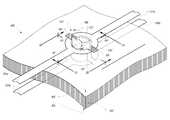
- FIG. 1is an isometric view of an embodiment of a portion of a circuit board substrate 100 having a dielectric layer 102 and an embodiment of a partitioned via 120 .
- the dielectric layer 102can have a top side 105 , a bottom side 106 , a via hole 108 , and first and second interconnects 110 - 111 within the via hole 108 .
- the via hole 108extends between the top and bottom sides 105 - 106 and includes a first sidewall section covered with a first metal wall plating 114 defining the first interconnect 110 and a second sidewall section covered with a second metal wall plating 115 defining the second interconnect 111 .
- the first and second wall platings 114 - 115can be formed from the same layer or “deposit” as explained in more detail below.
- the via hole 108can also include first and second partitions 118 - 119 that bisect the via hole 108 and define a gap that electrically isolates the first wall plating 114 from the second wall plating 115 .
- the first and second partitions 118 - 119can have partition walls cut through a metal layer deposited along the sidewall and cut into the dielectric material at the sidewall.
- the via 120can further include a dielectric plug 122 or spacer layer that fills the remainder of the via hole 108 .
- the dielectric plug 122can be attached to portions of the wall platings 114 - 115 and can also be attached to portions of the partitions 118 - 119 .
- the dielectric plug 122can protect the via 120 during subsequent manufacturing (e.g., circuit board layer stacking) and can also provide electrical or mechanical isolation between the wall platings 114 - 115 and metal lead land portions (described below).
- the dielectric plug 122may be omitted and the via hole 108 can be filled or partially filled with a gas or other type of intermediary material.
- the via 120is electrically coupled to metal contacts that are located on portions of the top side 105 or the bottom 106 side of the dielectric layer 102 .
- the circuit board 100can include first and second metal lead lands 130 - 131 , first metal traces 134 (identified individually by reference numbers 134 a - b ), and second metal traces 135 (identified individually by reference numbers 135 a - b ).
- the first lead land 130 and individual first and second traces 134 a and 135 aare attached at the top side 105 of the dielectric layer 102
- the second lead land 131 and individual first and second traces 134 b and 135 bare attached at the bottom side 106 of the dielectric layer 102 .
- the lead lands 130 - 131are coupled to the wall platings 114 - 115 of the via 120 . More specifically, the first traces 134 a - b are connected to the first interconnect 110 via the first and second lead lands 130 - 131 , and the second traces 135 a - b are similarly connected to the second interconnect 111 via the first and second lead lands 130 - 131 . In several embodiments, the partitions 118 - 119 separate a first portion of the lead lands 130 - 131 that are coupled to the first interconnect 110 from a second portion of the lead lands 130 - 131 that are coupled to the second interconnect 111 . Accordingly, the first traces 134 a - b and the second traces 135 a - b intercouple opposite sides of the dielectric layer 102 through separate conduction paths that both pass through the via hole 108 .
- FIG. 2Ais a cross-section of FIG. 1 along line 2 A- 2 A illustrating the circuit board 100 and a plated portion of the via 120 .
- This viewshows the dielectric layer 102 , the via 120 , the lead lands 130 - 131 , and the traces 134 - 135 .
- the dielectric layer 102can be plated with top- and bottom-side cladding layers 140 - 141 that are sandwiched between portions of the dielectric layer 102 and the interconnects 110 - 111 .
- the cladding layers 140 - 141 and the interconnects 110 - 111can have individual patterns that correspond to the shape of individual lead lands 130 - 131 (e.g., a ring) and individual traces 134 - 135 (e.g., a line).
- the via 120including the dielectric plug 122 , has a general shape that corresponds to the shape of the via hole 108 ( FIG. 1 ).
- a portion of the first interconnect 110i.e., the first wall plating 114
- a portion of the second interconnect 111(i.e., the second wall plating 115 ) is at another side of the dielectric plug 122 .
- the plug 122has partition regions that are defined by walls of the partitions 118 - 119 (drawn in phantom) that separate and electrically isolate the wall platings 114 - 115 from one another (described below).
- FIG. 2Bis a cross-section of FIG. 1 along line 2 B- 2 B illustrating the circuit board 100 and a non-plated portion of the via 120 .
- the dielectric layer 102can include the partitions 118 - 119 , which define lateral edges of first and second partition regions 150 - 151 (drawn in phantom) on the via 120 , or more specifically, on the dielectric plug 122 .
- the partition regions 150 - 151are also generally located between and electrically isolate portions of the lead lands 130 - 131 (also drawn in phantom).
- conventional viasoccupy a significant amount of surface area on a circuit board layer.
- the viasthemselves do not necessarily take up a large area, the lead land that surrounds the via can create a substantial footprint.
- Each viatypically needs to be surrounded by a lead land in order to accommodate an overlap tolerance with a metal contact (e.g., another via) on an above- or below-located circuit board layer.
- Most conventional circuit board layerstypically have design rules that require a minimum lead land diameter corresponding to this overlap tolerance. Such design rules can also establish a preferred spacing distance between individual traces (i.e., to conserve surface area).
- the via 120can conserve surface area on a circuit board layer by coupling multiple traces through an individual via hole.
- the via 120allows two separate metal traces to be electrically coupled through the circuit board 100 while only occupying a single lead land area.
- three or more metal tracescan be routed through a partitioned via.
- a via holecan be partitioned to have three or more separate sidewall portions that are individually plated with a metal layer.
- partitioned viasallow traces to be aligned in parallel without having to divert to separate vias. Such traces can be separated from each other by a fixed spacing distance and thus can allow electronic components to communicate differentially without impedance discontinuities (see, e.g., FIG. 9 ).
- FIGS. 3-7Billustrate stages of forming the partitioned via 120 in accordance with several embodiments of the disclosure.
- FIG. 3is a cross-sectional side view of the dielectric layer 102 and the cladding layers 140 - 141 .
- the dielectric layer 102includes a core material (e.g., G10/FR4 or other type of epoxy or glass based material) and the cladding layers 140 - 141 include a conductive material (e.g., copper, gold, or other type of cladding material that can be plated, laminated, or otherwise bonded).
- the dielectric layer 102can be part of a support base for a double-sided circuit board or be included in a stack of single- or double-sided circuit board layers.
- one or more of the cladding layers 140 - 141can be omitted (e.g., if the dielectric layer 102 is used as a single-sided circuit board layer).
- FIG. 4Ais a cross-sectional side view of the dielectric layer 102 after forming a first hole 160 , including a sidewall with first and second sidewall portions 164 - 165 , by a first patterning process.
- FIG. 4Bis a top-view of the dielectric layer 102 showing a shape (i.e., a circle) of the first hole 160 .
- the first patterning processremoves dielectric material from the dielectric layer 102 and can include mechanical drilling, laser drilling, or mechanical stamping through the dielectric layer 102 .
- Mechanical drilling processesuse an automated drilling machine having a drill bit that forms holes in the dielectric layer at pre-programmed locations.
- Laser drilling processespattern a dielectric layer in a similar fashion, but instead use a laser in lieu of a drill bit.
- the laserablates portions of the dielectric layer and thus creates relatively smaller holes than mechanically drilled holes.
- Mechanical stamping processescan also be automated and include the use of a stamping machine or punch tool. The stamping machine punches out dielectric material from the dielectric layer 102 , leaving a patterned void in the dielectric layer 102 .
- Other patterning processescan include various types of wet or dry chemical etching techniques and corresponding lithographic patterning and development steps.
- the first patterning processesmay incorporate the well developed chemical etching and lithography techniques of the semiconductor arts.
- the first patterning processcan be omitted.
- the dielectric layer 102for example, can be a substrate that has been pre-fabricated and includes individual pre-formed holes corresponding to the shape of the first hole 160 .
- FIG. 5is a cross-sectional side view of the dielectric layer 102 after forming a metal plating layer 170 that covers the sidewall portions 164 - 165 of the first hole 160 .
- the plating layer 170can be a material such as copper, aluminum, or an alloy of the two that is deposited onto the sidewall portions 164 - 165 .
- the plating layer 170can be formed using a process such as electroplating, electroless plating, or other types of thin film deposition techniques (e.g., physical and chemical vapor deposition).
- the plating layer 170also covers at least one of the cladding layers 140 - 141 .
- Stacked portions of the plating layer 170 and the cladding layers 140 - 141can be used to form the lead lands 130 - 131 and traces 134 - 135 (see, e.g., FIGS. 2A-B ).
- FIG. 6Ais a cross-sectional side view of the via hole 108 in the dielectric layer 102 formed by cutting the partitions 118 - 119 in the first hole 160 using a second patterning process.
- FIG. 6Bis a top view of the dielectric layer 102 showing a shape of the partitions 118 - 119 (e.g., rectilinear) of a partitioned via.
- the partitions 118 - 119generally correspond to sections where the second patterning process has removed portions of the plating layer 170 from the first hole 160 .
- the second patterning processfurther removes dielectric material from the dielectric layer 102 .
- the second patterning processcan also remove portions of the plating layer 170 and the cladding layers 140 - 141 from top- and bottom-side portions of the dielectric layer 102 that are adjacent to the partitions 118 - 119 .
- the second patterning processcan be similar to the first patterning process, but the second pattering process augments the first hole 160 to have a definable boundary between the sidewall portions 164 - 165 .
- any one of mechanical drilling, laser drilling, mechanical stamping, or chemical etchingcan be used to augment the first hole 160 by removing the portions of the plating layer 170 or dielectric material from the dielectric layer 102 .
- FIGS. 7A and 7Bare cross-sectional side views of the dielectric layer 102 after filling the via hole 108 with a dielectric spacer material 190 .
- the dielectric spacer material 190may be a non-conductive ink that is held by surface tension to the plating layer 170 and the walls of the partitions 118 - 119 .
- the dielectric spacer material 190is a conformal and non-conductive film that is deposited or otherwise formed in the via hole 108 .
- excess dielectric material 190can be etched, compressed, planarized, or otherwise removed from top- or bottom-side surfaces of the dielectric layer 102 .
- the plating layer 170 and the cladding layers 140 - 141can be patterned to form the lead lands 130 - 131 and the traces 134 - 135 .
- the dielectric layer 102may be covered in a photolithographic film that is patterned, developed, and subsequently etched to create the shape of the leads lands 130 - 131 and the traces 134 - 135 (e.g., via a wet or dry etch).
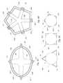
- Embodiments of the partitioned via 120can have any of a wide variety of different shapes that can be adapted by modifying the shape of the via hole 108 .
- FIG. 8Ais a top view of an embodiment of an elliptical via 220 having a plurality of elliptically segmented lead lands 230 a - d .
- An elliptically shaped hole 260 and partition cuts using a cross-shaped cutting pattern 280can form four separate partition regions 250 - 253 between the lead lands 230 a - d .
- the via 220can route up to four separate electrical connections through a circuit board layer via the lead lands 230 a - d .
- FIG. 8Ais a top view of an embodiment of an elliptical via 220 having a plurality of elliptically segmented lead lands 230 a - d .
- FIG. 8Bis top view of a via 320 having a plurality of lead land 330 a - d that have a pentagon shape.
- a pentagon shaped hole 360 and a branched cutting pattern 380can form five separate partition regions 350 - 354 electrically separating the lead lands 330 a - e . Accordingly, the partition regions 350 - 354 allow up to five electrical connection to be routed through the via 320 .
- the vias and lead landsmay have other types of circular, elliptical, polygonal shapes (e.g., a triangle, a square, a hexagon, etc.), or combinations thereof.
- FIG. 8Cshows top views of a triangular hole 460 , a square hole 560 , and a pentagon hole 660 that have been formed by a mechanical stamping process.
- a second patterning processcan create a circular augmentation 480 that yields three separate wall platings 414 - 416 in the triangular hole 460 , four separate wall platings 514 - 517 in the square hole 560 , and five separate wall platings 614 - 618 in the polygon hole 660 .
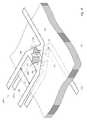
- FIG. 9is an isometric view of a portion of a circuit board layer 700 having a dielectric layer 702 and an embodiment of a triangular shaped via 720 .
- the dielectric layer 702can include a star shaped via hole 708 that includes partitions 717 - 719 .
- the via 720can include metal wall platings 714 - 716 that are separated by individual partitions 717 - 719 , and may further include a dielectric plug (not shown).
- the via 720may also be at least partially surrounded by triangular shaped metal lead lands 730 - 731 that are located at opposite sides of the dielectric layer 702 .
- the via 720can electrically intercouple individual metal traces 734 - 735 and sets of parallel metal traces 737 - 738 , which are separated from each by a fixed distances d 1 .
- the fixed distance d 1does not increase when the sets of traces 737 - 738 route through the via hole 708 (mitigating variations in differential impedance).
- two or more electronic componentscan be electrically coupled together in a single-ended fashion using the individual traces 731 - 732 or differentially using the sets of traces 737 - 738 .
- the electronic componentsmay be attached to opposite sides of the circuit board layer 702 .
- an individual circuit board layer or a stacked system of such circuit board layersmay include one or more embodiments of a partitioned via.
- FIG. 10is a cross-sectional side view of a circuit board system 800 having individual circuit board layers 801 - 805 or stacking layers that are intercoupled by one or more partitioned vias 820 - 823 .
- the stacking layers 801 - 805have individual surfaces that include traces, lead lands, and other metal contacts that are electrically coupled to an above- or below-located stacking layer through one or more of the vias 820 - 823 .
- Individual viascan be formed, for example, by removing dielectric material from one or more of the stacking layers 801 - 805 and creating a via hole that extends through at least one of the stacking layers or towards one or more of the metal contacts located at any one of the stacking layers.
- the vias 820 - 821are “blind” vias that are aligned with metal contacts that are located at the circuit board layers 801 and 803 , respectively.
- the via 822is a “buried” via sandwiched between the circuit board layers 802 and 804 .
- the via 823is a “through-hole” via that electrically intercouples the top and bottom sides of the system 800 .
- the system 800can further include dielectric laminating layers 870 - 871 at the top and bottom sides of the system. Portions of the laminating layers 870 - 871 may expose electrical contacts that can include a gold and/or nickel plating layer 850 (to prevent rapid oxidation of copper based cladding and plating layers).
- a variety of electronic or microelectronic componentsare attached to the top or bottom sides of the system 800 .
- An electronic componentmay have one or more contacts that are electrically coupled to any one of the exposed contacts of the system 800 (e.g., by wire bonding or soldering).
- the system 800includes more or fewer circuit board layers.
- the system 990can include a processor 991 , a memory 992 (e.g., SRAM, DRAM, Flash, or other memory device), input/output devices 993 , or other subsystems or components 994 .
- Electronic devicesmay be included in any of the components shown in FIG. 11 .
- the resulting system 990can perform any of a wide variety of computing, processing, storage, sensor, imaging, or other functions.
- representative systems 990include, without limitation, computers or other data processors, for example, desktop computers, laptop computers, Internet appliances, hand-held devices (e.g., palm-top computers, wearable computers, cellular or mobile phones, personal digital assistants), multi-processor systems, processor-based or programmable consumer electronics, network computers, and minicomputers.
- Other representative systems 990include cameras, light or other radiation sensors, servers and associated server subsystems, display devices, or memory devices.
- Components of the system 990may be housed in a single unit or distributed over multiple, interconnected units, e.g., through a communications network. Components can accordingly include local or remote memory storage devices and any of a wide variety of computer-readable media.
Landscapes
- Engineering & Computer Science (AREA)
- Microelectronics & Electronic Packaging (AREA)
- Manufacturing & Machinery (AREA)
- Physics & Mathematics (AREA)
- Condensed Matter Physics & Semiconductors (AREA)
- General Physics & Mathematics (AREA)
- Computer Hardware Design (AREA)
- Power Engineering (AREA)
- Production Of Multi-Layered Print Wiring Board (AREA)
- Internal Circuitry In Semiconductor Integrated Circuit Devices (AREA)
Abstract
Description
Claims (14)
Priority Applications (2)
| Application Number | Priority Date | Filing Date | Title |
|---|---|---|---|
| US12/898,891US8367538B2 (en) | 2007-08-31 | 2010-10-06 | Partitioned through-layer via and associated systems and methods |
| US13/757,295US8536046B2 (en) | 2007-08-31 | 2013-02-01 | Partitioned through-layer via and associated systems and methods |
Applications Claiming Priority (4)
| Application Number | Priority Date | Filing Date | Title |
|---|---|---|---|
| SG200706414-0ASG150410A1 (en) | 2007-08-31 | 2007-08-31 | Partitioned through-layer via and associated systems and methods |
| SG200706414-0 | 2007-08-31 | ||
| US11/863,579US7830018B2 (en) | 2007-08-31 | 2007-09-28 | Partitioned through-layer via and associated systems and methods |
| US12/898,891US8367538B2 (en) | 2007-08-31 | 2010-10-06 | Partitioned through-layer via and associated systems and methods |
Related Parent Applications (1)
| Application Number | Title | Priority Date | Filing Date |
|---|---|---|---|
| US11/863,579DivisionUS7830018B2 (en) | 2007-08-31 | 2007-09-28 | Partitioned through-layer via and associated systems and methods |
Related Child Applications (1)
| Application Number | Title | Priority Date | Filing Date |
|---|---|---|---|
| US13/757,295DivisionUS8536046B2 (en) | 2007-08-31 | 2013-02-01 | Partitioned through-layer via and associated systems and methods |
Publications (2)
| Publication Number | Publication Date |
|---|---|
| US20110019372A1 US20110019372A1 (en) | 2011-01-27 |
| US8367538B2true US8367538B2 (en) | 2013-02-05 |
Family
ID=40406164
Family Applications (3)
| Application Number | Title | Priority Date | Filing Date |
|---|---|---|---|
| US11/863,579Active2027-11-01US7830018B2 (en) | 2007-08-31 | 2007-09-28 | Partitioned through-layer via and associated systems and methods |
| US12/898,891Active2028-02-08US8367538B2 (en) | 2007-08-31 | 2010-10-06 | Partitioned through-layer via and associated systems and methods |
| US13/757,295ActiveUS8536046B2 (en) | 2007-08-31 | 2013-02-01 | Partitioned through-layer via and associated systems and methods |
Family Applications Before (1)
| Application Number | Title | Priority Date | Filing Date |
|---|---|---|---|
| US11/863,579Active2027-11-01US7830018B2 (en) | 2007-08-31 | 2007-09-28 | Partitioned through-layer via and associated systems and methods |
Family Applications After (1)
| Application Number | Title | Priority Date | Filing Date |
|---|---|---|---|
| US13/757,295ActiveUS8536046B2 (en) | 2007-08-31 | 2013-02-01 | Partitioned through-layer via and associated systems and methods |
Country Status (2)
| Country | Link |
|---|---|
| US (3) | US7830018B2 (en) |
| SG (1) | SG150410A1 (en) |
Cited By (2)
| Publication number | Priority date | Publication date | Assignee | Title |
|---|---|---|---|---|
| US9281211B2 (en) | 2014-02-10 | 2016-03-08 | International Business Machines Corporation | Nanoscale interconnect structure |
| US20230008736A1 (en)* | 2019-12-17 | 2023-01-12 | Nitto Denko Corporation | Manufacturing method for double-sided wiring circuit board and double- sided wiring circuit board |
Families Citing this family (51)
| Publication number | Priority date | Publication date | Assignee | Title |
|---|---|---|---|---|
| US8084866B2 (en) | 2003-12-10 | 2011-12-27 | Micron Technology, Inc. | Microelectronic devices and methods for filling vias in microelectronic devices |
| US20050247894A1 (en) | 2004-05-05 | 2005-11-10 | Watkins Charles M | Systems and methods for forming apertures in microfeature workpieces |
| SG120200A1 (en) | 2004-08-27 | 2006-03-28 | Micron Technology Inc | Slanted vias for electrical circuits on circuit boards and other substrates |
| US7300857B2 (en) | 2004-09-02 | 2007-11-27 | Micron Technology, Inc. | Through-wafer interconnects for photoimager and memory wafers |
| US7795134B2 (en) | 2005-06-28 | 2010-09-14 | Micron Technology, Inc. | Conductive interconnect structures and formation methods using supercritical fluids |
| US7863187B2 (en) | 2005-09-01 | 2011-01-04 | Micron Technology, Inc. | Microfeature workpieces and methods for forming interconnects in microfeature workpieces |
| US7262134B2 (en) | 2005-09-01 | 2007-08-28 | Micron Technology, Inc. | Microfeature workpieces and methods for forming interconnects in microfeature workpieces |
| US7749899B2 (en) | 2006-06-01 | 2010-07-06 | Micron Technology, Inc. | Microelectronic workpieces and methods and systems for forming interconnects in microelectronic workpieces |
| US7629249B2 (en) | 2006-08-28 | 2009-12-08 | Micron Technology, Inc. | Microfeature workpieces having conductive interconnect structures formed by chemically reactive processes, and associated systems and methods |
| US7902643B2 (en) | 2006-08-31 | 2011-03-08 | Micron Technology, Inc. | Microfeature workpieces having interconnects and conductive backplanes, and associated systems and methods |
| FR2910706B1 (en)* | 2006-12-21 | 2009-03-20 | Commissariat Energie Atomique | INTERCONNECTION ELEMENT BASED ON CARBON NANOTUBES |
| SG149710A1 (en) | 2007-07-12 | 2009-02-27 | Micron Technology Inc | Interconnects for packaged semiconductor devices and methods for manufacturing such devices |
| SG150410A1 (en) | 2007-08-31 | 2009-03-30 | Micron Technology Inc | Partitioned through-layer via and associated systems and methods |
| US7884015B2 (en) | 2007-12-06 | 2011-02-08 | Micron Technology, Inc. | Methods for forming interconnects in microelectronic workpieces and microelectronic workpieces formed using such methods |
| US8084854B2 (en) | 2007-12-28 | 2011-12-27 | Micron Technology, Inc. | Pass-through 3D interconnect for microelectronic dies and associated systems and methods |
| US8253230B2 (en) | 2008-05-15 | 2012-08-28 | Micron Technology, Inc. | Disabling electrical connections using pass-through 3D interconnects and associated systems and methods |
| US9064717B2 (en)* | 2008-09-26 | 2015-06-23 | International Business Machines Corporation | Lock and key through-via method for wafer level 3D integration and structures produced thereby |
| KR20100037387A (en)* | 2008-10-01 | 2010-04-09 | 삼성전자주식회사 | Memory moduel and topology of circuit board |
| CN101494951A (en)* | 2009-02-18 | 2009-07-29 | 旭丽电子(广州)有限公司 | Printed circuit board |
| US9406561B2 (en)* | 2009-04-20 | 2016-08-02 | International Business Machines Corporation | Three dimensional integrated circuit integration using dielectric bonding first and through via formation last |
| TWI479968B (en)* | 2009-09-09 | 2015-04-01 | Advanced Semiconductor Eng | Fabrication method of circuit board, circuit board, and chip package structure |
| US8519542B2 (en)* | 2010-08-03 | 2013-08-27 | Xilinx, Inc. | Air through-silicon via structure |
| KR101736984B1 (en)* | 2010-09-16 | 2017-05-17 | 삼성전자 주식회사 | Print circuit board having hexagonal bump pad for substrate of semiconductor package and semiconductor package having the same |
| WO2012045000A1 (en)* | 2010-09-30 | 2012-04-05 | Aviat Networks, Inc. | Systems and methods for improved chip device performance |
| US20120319293A1 (en)* | 2011-06-17 | 2012-12-20 | Bok Eng Cheah | Microelectronic device, stacked die package and computing system containing same, method of manufacturing a multi-channel communication pathway in same, and method of enabling electrical communication between components of a stacked-die package |
| US8541884B2 (en)* | 2011-07-06 | 2013-09-24 | Research Triangle Institute | Through-substrate via having a strip-shaped through-hole signal conductor |
| US8847364B2 (en)* | 2011-10-03 | 2014-09-30 | Marvell World Trade Ltd. | Removing conductive material to form conductive features in a substrate |
| CN102724807A (en)* | 2012-06-08 | 2012-10-10 | 加弘科技咨询(上海)有限公司 | Printed circuit board |
| US8563403B1 (en) | 2012-06-27 | 2013-10-22 | International Business Machines Corporation | Three dimensional integrated circuit integration using alignment via/dielectric bonding first and through via formation last |
| US20140034363A1 (en)* | 2012-08-01 | 2014-02-06 | Samtec, Inc. | Multi-layer transmission lines |
| US8791016B2 (en) | 2012-09-25 | 2014-07-29 | International Business Machines Corporation | Through silicon via wafer, contacts and design structures |
| US10103447B2 (en) | 2014-06-13 | 2018-10-16 | Nxp Usa, Inc. | Integrated circuit package with radio frequency coupling structure |
| US9917372B2 (en) | 2014-06-13 | 2018-03-13 | Nxp Usa, Inc. | Integrated circuit package with radio frequency coupling arrangement |
| US10225925B2 (en)* | 2014-08-29 | 2019-03-05 | Nxp Usa, Inc. | Radio frequency coupling and transition structure |
| US9887449B2 (en)* | 2014-08-29 | 2018-02-06 | Nxp Usa, Inc. | Radio frequency coupling structure and a method of manufacturing thereof |
| CN107251660B (en) | 2015-02-20 | 2022-08-26 | 奈科斯特金技术私人有限公司 | Method for manufacturing printed circuit board |
| EP3501241A4 (en) | 2016-08-19 | 2020-08-12 | Nextgin Technology B.v. | METHOD OF MANUFACTURING A PRESSURE PCB |
| CN110999547B (en)* | 2017-08-21 | 2023-04-18 | 住友电工印刷电路株式会社 | Printed wiring board |
| JP7032128B2 (en)* | 2017-12-25 | 2022-03-08 | 住友電工プリントサーキット株式会社 | Manufacturing method of printed wiring board and printed wiring board |
| KR102611780B1 (en)* | 2018-10-26 | 2023-12-11 | 삼성전자 주식회사 | Electronic device and substrate connecting member comprising opening surrounding region where through wiring is formed and substrate having conductive member formed on the side of the opening |
| KR102828851B1 (en)* | 2018-11-19 | 2025-07-03 | 삼성디스플레이 주식회사 | A substate and a display device including the same |
| US10763203B1 (en)* | 2019-02-08 | 2020-09-01 | Nxp B.V. | Conductive trace design for smart card |
| US12034053B2 (en) | 2019-05-30 | 2024-07-09 | National Research Council Of Canada | Ohmic contacts with direct access pathways to two-dimensional electron sheets |
| US11234325B2 (en) | 2019-06-20 | 2022-01-25 | Infinera Corporation | Printed circuit board having a differential pair routing topology with negative plane routing and impedance correction structures |
| CN110572935A (en)* | 2019-08-27 | 2019-12-13 | 沪士电子股份有限公司 | vertical conductor PCB and processing method thereof |
| CN113133192A (en)* | 2019-12-31 | 2021-07-16 | 华为技术有限公司 | Multilayer circuit board, electronic device, and multilayer circuit board processing method |
| WO2023287569A1 (en)* | 2021-07-13 | 2023-01-19 | Corning Incorporated | Vias including a plurality of traces, devices including the vias, and methods for fabricating the vias |
| CN114698233B (en)* | 2022-04-27 | 2023-08-22 | 苏州浪潮智能科技有限公司 | PCB signal via structure, and determination method, determination device and determination equipment thereof |
| US11832383B1 (en)* | 2022-07-13 | 2023-11-28 | Western Digital Technologies, Inc. | Shared vias for differential pair trace routing |
| CN115942601A (en)* | 2022-10-31 | 2023-04-07 | 苏州浪潮智能科技有限公司 | Circuit board, electronic equipment and circuit board manufacturing method |
| JP7720500B1 (en)* | 2024-12-12 | 2025-08-07 | 住友電気工業株式会社 | printed wiring board |
Citations (449)
| Publication number | Priority date | Publication date | Assignee | Title |
|---|---|---|---|---|
| US2821959A (en) | 1956-03-29 | 1958-02-04 | Bell Telephone Labor Inc | Mass soldering of electrical assemblies |
| US3006318A (en) | 1958-03-26 | 1961-10-31 | Western Electric Co | Apparatus for applying solder coatings to surfaces |
| US3345134A (en) | 1962-04-21 | 1967-10-03 | Knapsack Ag | Process and apparatus for the manufacture of titanium nitride |
| US3865298A (en) | 1973-08-14 | 1975-02-11 | Atomic Energy Commission | Solder leveling |
| US3902036A (en) | 1974-05-02 | 1975-08-26 | Western Electric Co | Control system using multiplexed laser beams |
| US4040168A (en) | 1975-11-24 | 1977-08-09 | Rca Corporation | Fabrication method for a dual gate field-effect transistor |
| US4368106A (en) | 1980-10-27 | 1983-01-11 | General Electric Company | Implantation of electrical feed-through conductors |
| EP0127946A1 (en) | 1983-05-10 | 1984-12-12 | BRITISH TELECOMMUNICATIONS public limited company | Method of producing a via in a semiconductor device |
| US4534100A (en) | 1982-06-28 | 1985-08-13 | The United States Of America As Represented By The Secretary Of The Air Force | Electrical method of making conductive paths in silicon |
| US4581301A (en) | 1984-04-10 | 1986-04-08 | Michaelson Henry W | Additive adhesive based process for the manufacture of printed circuit boards |
| US4608480A (en) | 1983-06-15 | 1986-08-26 | S.N.E.C.M.A. | Process and apparatus for laser drilling |
| US4614427A (en) | 1983-05-20 | 1986-09-30 | Hitachi, Ltd. | Automatic contaminants detection apparatus |
| US4627971A (en) | 1985-04-22 | 1986-12-09 | Alza Corporation | Osmotic device with self-sealing passageway |
| US4660063A (en) | 1985-03-18 | 1987-04-21 | General Electric Company | Immersion type ISFET |
| JPS6352432A (en) | 1986-08-22 | 1988-03-05 | Hitachi Vlsi Eng Corp | semiconductor equipment |
| US4756765A (en) | 1982-01-26 | 1988-07-12 | Avco Research Laboratory, Inc. | Laser removal of poor thermally-conductive materials |
| US4768291A (en) | 1987-03-12 | 1988-09-06 | Monarch Technologies Corporation | Apparatus for dry processing a semiconductor wafer |
| US4818728A (en) | 1986-12-03 | 1989-04-04 | Sharp Kabushiki Kaisha | Method of making a hybrid semiconductor device |
| US4907127A (en) | 1988-03-21 | 1990-03-06 | Lee John K C | Printed circuit board construction and method for producing printed circuit end products |
| US4959705A (en) | 1988-10-17 | 1990-09-25 | Ford Microelectronics, Inc. | Three metal personalization of application specific monolithic microwave integrated circuit |
| US4964212A (en) | 1988-09-29 | 1990-10-23 | Commissariat A L'energie Atomique | Process for producing electrical connections through a substrate |
| US4984597A (en) | 1984-05-21 | 1991-01-15 | Cfm Technologies Research Associates | Apparatus for rinsing and drying surfaces |
| US5024966A (en) | 1988-12-21 | 1991-06-18 | At&T Bell Laboratories | Method of forming a silicon-based semiconductor optical device mount |
| US5026964A (en) | 1986-02-28 | 1991-06-25 | General Electric Company | Optical breakthrough sensor for laser drill |
| US5027184A (en) | 1981-03-02 | 1991-06-25 | Rockwell International Corporation | NPN type lateral transistor with minimal substrate operation interference |
| US5037782A (en) | 1989-03-29 | 1991-08-06 | Mitsubishi Denki Kabushiki Kaisha | Method of making a semiconductor device including via holes |
| US5123902A (en) | 1988-09-13 | 1992-06-23 | Carl-Zeiss-Stiftung | Method and apparatus for performing surgery on tissue wherein a laser beam is applied to the tissue |
| US5145099A (en) | 1990-07-13 | 1992-09-08 | Micron Technology, Inc. | Method for combining die attach and lead bond in the assembly of a semiconductor package |
| US5158911A (en) | 1990-08-03 | 1992-10-27 | Thomson Composants Microondes | Method for interconnection between an integrated circuit and a support circuit, and integrated circuit adapted to this method |
| US5219344A (en) | 1988-06-09 | 1993-06-15 | Visx, Incorporated | Methods and apparatus for laser sculpture of the cornea |
| US5233448A (en) | 1992-05-04 | 1993-08-03 | Industrial Technology Research Institute | Method of manufacturing a liquid crystal display panel including photoconductive electrostatic protection |
| US5237148A (en) | 1990-10-04 | 1993-08-17 | Brother Kogyo Kabushiki | Device for manufacturing a nozzle and its manufacturing method |
| US5289631A (en) | 1992-03-04 | 1994-03-01 | Mcnc | Method for testing, burn-in, and/or programming of integrated circuit chips |
| US5292686A (en) | 1991-08-21 | 1994-03-08 | Triquint Semiconductor, Inc. | Method of forming substrate vias in a GaAs wafer |
| US5294568A (en) | 1990-10-12 | 1994-03-15 | Genus, Inc. | Method of selective etching native oxide |
| US5304743A (en) | 1992-05-12 | 1994-04-19 | Lsi Logic Corporation | Multilayer IC semiconductor package |
| US5378312A (en) | 1993-12-07 | 1995-01-03 | International Business Machines Corporation | Process for fabricating a semiconductor structure having sidewalls |
| US5378313A (en) | 1993-12-22 | 1995-01-03 | Pace; Benedict G. | Hybrid circuits and a method of manufacture |
| US5380681A (en) | 1994-03-21 | 1995-01-10 | United Microelectronics Corporation | Three-dimensional multichip package and methods of fabricating |
| US5402435A (en) | 1993-03-05 | 1995-03-28 | Matsushita Electric Industrial Co., Ltd. | Optical device |
| US5406630A (en) | 1992-05-04 | 1995-04-11 | Motorola, Inc. | Tamperproof arrangement for an integrated circuit device |
| US5424573A (en) | 1992-03-04 | 1995-06-13 | Hitachi, Ltd. | Semiconductor package having optical interconnection access |
| TW250597B (en) | 1993-06-04 | 1995-07-01 | Framatome & Cie | |
| US5438212A (en) | 1993-02-25 | 1995-08-01 | Mitsubishi Denki Kabushiki Kaisha | Semiconductor device with heat dissipation structure |
| US5447871A (en) | 1993-03-05 | 1995-09-05 | Goldstein; Edward F. | Electrically conductive interconnection through a body of semiconductor material |
| US5464960A (en) | 1993-01-12 | 1995-11-07 | Iatrotech, Inc. | Laser calibration device |
| US5481483A (en) | 1992-11-23 | 1996-01-02 | Ford Motor Company | Non-contact method of obtaining dimensional information about an object for comparing similar objects |
| US5496755A (en) | 1989-11-29 | 1996-03-05 | Texas Instruments Incorporated | Integrated circuit and method |
| US5515167A (en) | 1994-09-13 | 1996-05-07 | Hughes Aircraft Company | Transparent optical chuck incorporating optical monitoring |
| US5518956A (en) | 1993-09-02 | 1996-05-21 | General Electric Company | Method of isolating vertical shorts in an electronic array using laser ablation |
| US5585308A (en) | 1993-12-23 | 1996-12-17 | Sgs-Thomson Microelectronics, Inc. | Method for improved pre-metal planarization |
| US5585675A (en) | 1994-05-11 | 1996-12-17 | Harris Corporation | Semiconductor die packaging tub having angularly offset pad-to-pad via structure configured to allow three-dimensional stacking and electrical interconnections among multiple identical tubs |
| US5614743A (en) | 1994-07-26 | 1997-03-25 | Kabushiki Kaisha Toshiba | Microwave integrated circuit (MIC) having a reactance element formed on a groove |
| US5618752A (en) | 1995-06-05 | 1997-04-08 | Harris Corporation | Method of fabrication of surface mountable integrated circuits |
| US5624437A (en) | 1995-03-28 | 1997-04-29 | Freeman; Jerre M. | High resolution, high speed, programmable laser beam modulating apparatus for microsurgery |
| US5627106A (en) | 1994-05-06 | 1997-05-06 | United Microelectronics Corporation | Trench method for three dimensional chip connecting during IC fabrication |
| US5646067A (en) | 1995-06-05 | 1997-07-08 | Harris Corporation | Method of bonding wafers having vias including conductive material |
| US5654221A (en) | 1994-10-17 | 1997-08-05 | International Business Machines Corporation | Method for forming semiconductor chip and electronic module with integrated surface interconnects/components |
| US5673846A (en) | 1995-08-24 | 1997-10-07 | International Business Machines Corporation | Solder anchor decal and method |
| US5684642A (en) | 1994-02-22 | 1997-11-04 | Mitsubishi Denki Kabushiki Kaisha | Optical transmission system and light radiating method |
| US5690841A (en) | 1993-12-10 | 1997-11-25 | Pharmacia Biotech Ab | Method of producing cavity structures |
| US5718791A (en) | 1995-06-05 | 1998-02-17 | R + S Stanztechnik Gmbh | Method of laminating a trim panel and folding a cover sheet edge around the panel rim |
| US5723904A (en) | 1993-03-10 | 1998-03-03 | Sumitomo Electric Industries, Ltd. | Packaged semiconductor device suitable to be mounted and connected to microstrip line structure board |
| US5726493A (en) | 1994-06-13 | 1998-03-10 | Fujitsu Limited | Semiconductor device and semiconductor device unit having ball-grid-array type package structure |
| US5771158A (en) | 1995-09-21 | 1998-06-23 | Mitsubishi Denki Kabushiki Kaisha | Printed circuit board, printed circuit board used for flat panel display drive circuit, and flat panel display device |
| US5773359A (en) | 1995-12-26 | 1998-06-30 | Motorola, Inc. | Interconnect system and method of fabrication |
| US5776824A (en) | 1995-12-22 | 1998-07-07 | Micron Technology, Inc. | Method for producing laminated film/metal structures for known good die ("KG") applications |
| US5807439A (en) | 1997-09-29 | 1998-09-15 | Siemens Aktiengesellschaft | Apparatus and method for improved washing and drying of semiconductor wafers |
| US5811799A (en) | 1997-07-31 | 1998-09-22 | Wu; Liang-Chung | Image sensor package having a wall with a sealed cover |
| US5821532A (en) | 1997-06-16 | 1998-10-13 | Eastman Kodak Company | Imager package substrate |
| US5825080A (en) | 1995-12-18 | 1998-10-20 | Atr Optical And Radio Communications Research Laboratories | Semiconductor device provided with surface grounding conductor for covering surfaces of electrically insulating films |
| US5826628A (en) | 1996-01-24 | 1998-10-27 | Micron Technology, Inc. | Form tooling and method of forming semiconductor package leads |
| US5847454A (en) | 1993-02-04 | 1998-12-08 | Cornell Research Foundcatton, Inc. | Electrically isolated released microstructures |
| US5851845A (en) | 1995-12-18 | 1998-12-22 | Micron Technology, Inc. | Process for packaging a semiconductor die using dicing and testing |
| US5857963A (en) | 1996-07-17 | 1999-01-12 | Welch Allyn, Inc. | Tab imager assembly for use in an endoscope |
| US5861654A (en) | 1995-11-28 | 1999-01-19 | Eastman Kodak Company | Image sensor assembly |
| US5870289A (en) | 1994-12-15 | 1999-02-09 | Hitachi, Ltd. | Chip connection structure having diret through-hole connections through adhesive film and wiring substrate |
| US5870823A (en) | 1996-11-27 | 1999-02-16 | International Business Machines Corporation | Method of forming a multilayer electronic packaging substrate with integral cooling channels |
| US5893828A (en) | 1996-05-02 | 1999-04-13 | Uram; Martin | Contact laser surgical endoscope and associated myringotomy procedure |
| US5904499A (en) | 1994-12-22 | 1999-05-18 | Pace; Benedict G | Package for power semiconductor chips |
| US5969422A (en) | 1997-05-15 | 1999-10-19 | Advanced Micro Devices, Inc. | Plated copper interconnect structure |
| US5998292A (en) | 1997-11-12 | 1999-12-07 | International Business Machines Corporation | Method for making three dimensional circuit integration |
| US5998240A (en) | 1996-07-22 | 1999-12-07 | Northrop Grumman Corporation | Method of extracting heat from a semiconductor body and forming microchannels therein |
| US6004867A (en) | 1996-12-16 | 1999-12-21 | Samsung Electronics Co., Ltd. | Chip-size packages assembled using mass production techniques at the wafer-level |
| US6008070A (en) | 1998-05-21 | 1999-12-28 | Micron Technology, Inc. | Wafer level fabrication and assembly of chip scale packages |
| US6008914A (en) | 1994-04-28 | 1999-12-28 | Mitsubishi Denki Kabushiki Kaisha | Laser transfer machining apparatus |
| US6080291A (en) | 1998-07-10 | 2000-06-27 | Semitool, Inc. | Apparatus for electrochemically processing a workpiece including an electrical contact assembly having a seal member |
| US6097087A (en) | 1997-10-31 | 2000-08-01 | Micron Technology, Inc. | Semiconductor package including flex circuit, interconnects and dense array external contacts |
| US6103547A (en) | 1997-01-17 | 2000-08-15 | Micron Technology, Inc. | High speed IC package configuration |
| US6107679A (en) | 1997-12-22 | 2000-08-22 | Oki Electric Industry Co., Ltd. | Semiconductor device |
| US6107180A (en) | 1998-01-30 | 2000-08-22 | Motorola, Inc. | Method for forming interconnect bumps on a semiconductor die |
| US6110825A (en) | 1997-11-26 | 2000-08-29 | Stmicroelectronics, S.R.L. | Process for forming front-back through contacts in micro-integrated electronic devices |
| US6114240A (en) | 1997-12-18 | 2000-09-05 | Micron Technology, Inc. | Method for fabricating semiconductor components using focused laser beam |
| US6119335A (en) | 1997-12-02 | 2000-09-19 | Samsung Electro-Mechanics Co., Ltd. | Method for manufacturing multi-layer printed circuit board |
| US6124634A (en) | 1996-03-07 | 2000-09-26 | Micron Technology, Inc. | Micromachined chip scale package |
| US6130141A (en) | 1998-10-14 | 2000-10-10 | Lucent Technologies Inc. | Flip chip metallization |
| US6137182A (en) | 1996-07-23 | 2000-10-24 | Advanced Micro Devices, Inc. | Method of reducing via and contact dimensions beyond photolithography equipment limits |
| US6140604A (en) | 1998-06-18 | 2000-10-31 | General Electric Company | Laser drilling breakthrough detector |
| US6143588A (en) | 1997-09-09 | 2000-11-07 | Amkor Technology, Inc. | Method of making an integrated circuit package employing a transparent encapsulant |
| US6148509A (en) | 1997-04-07 | 2000-11-21 | Micron Technology, Inc. | Method for supporting an integrated circuit die |
| US6159764A (en) | 1997-07-02 | 2000-12-12 | Micron Technology, Inc. | Varied-thickness heat sink for integrated circuit (IC) packages and method of fabricating IC packages |
| US6180518B1 (en) | 1999-10-29 | 2001-01-30 | Lucent Technologies Inc. | Method for forming vias in a low dielectric constant material |
| US6184465B1 (en) | 1998-11-12 | 2001-02-06 | Micron Technology, Inc. | Semiconductor package |
| US6184060B1 (en) | 1996-10-29 | 2001-02-06 | Trusi Technologies Llc | Integrated circuits and methods for their fabrication |
| US6187615B1 (en) | 1998-08-28 | 2001-02-13 | Samsung Electronics Co., Ltd. | Chip scale packages and methods for manufacturing the chip scale packages at wafer level |
| US6191487B1 (en) | 1998-04-23 | 2001-02-20 | Minco Technology Labs, Inc. | Semiconductor and flip chip packages and method having a back-side connection |
| KR20010018694A (en) | 1999-08-21 | 2001-03-15 | 윤종용 | Manufacturing method for three demensional stack chip package |
| US6203539B1 (en) | 1993-05-07 | 2001-03-20 | Visx, Incorporated | Method and system for laser treatment of refractive errors using offset imaging |
| JP2001077496A (en) | 1999-09-06 | 2001-03-23 | Ngk Insulators Ltd | Substrate for printed circuit and its manufacture |
| JP2001082931A (en) | 1999-09-09 | 2001-03-30 | Toshiba Corp | Hole depth measuring method and hole depth measuring device |
| US6222136B1 (en) | 1997-11-12 | 2001-04-24 | International Business Machines Corporation | Printed circuit board with continuous connective bumps |
| US6222270B1 (en) | 1997-06-24 | 2001-04-24 | Samsung Electronics Co., Ltd. | Integrated circuit bonding pads including closed vias and closed conductive patterns |
| US6221769B1 (en) | 1999-03-05 | 2001-04-24 | International Business Machines Corporation | Method for integrated circuit power and electrical connections via through-wafer interconnects |
| US6228687B1 (en) | 1999-06-28 | 2001-05-08 | Micron Technology, Inc. | Wafer-level package and methods of fabricating |
| US6229202B1 (en) | 2000-01-10 | 2001-05-08 | Micron Technology, Inc. | Semiconductor package having downset leadframe for reducing package bow |
| US6235552B1 (en) | 1999-07-09 | 2001-05-22 | Samsung Electronics Co., Ltd. | Chip scale package and method for manufacturing the same using a redistribution substrate |
| US6246108B1 (en) | 1997-09-15 | 2001-06-12 | Micron Technology, Inc. | Integrated circuit package including lead frame with electrically isolated alignment feature |
| US6252300B1 (en) | 1999-01-14 | 2001-06-26 | United Microelectronics Corp. | Direct contact through hole type wafer structure |
| US6268114B1 (en) | 1998-09-18 | 2001-07-31 | Taiwan Semiconductor Manufacturing Company, Ltd | Method for forming fine-pitched solder bumps |
| US6271580B1 (en) | 1996-12-30 | 2001-08-07 | Micron Technology, Inc. | Leads under chip in conventional IC package |
| US6277757B1 (en) | 1999-06-01 | 2001-08-21 | Winbond Electronics Corp. | Methods to modify wet by dry etched via profile |
| US20010020739A1 (en) | 2000-03-09 | 2001-09-13 | Nec Corporation | Flip chip type semiconductor device and method for manufacturing the same |
| US6291894B1 (en) | 1998-08-31 | 2001-09-18 | Micron Technology, Inc. | Method and apparatus for a semiconductor package for vertical surface mounting |
| US6294837B1 (en) | 1997-12-18 | 2001-09-25 | Micron Technology, Inc. | Semiconductor interconnect having laser machined contacts |
| US6297155B1 (en) | 1999-05-03 | 2001-10-02 | Motorola Inc. | Method for forming a copper layer over a semiconductor wafer |
| JP2001298147A (en) | 2000-04-18 | 2001-10-26 | Kawasaki Steel Corp | Semiconductor device and manufacturing method thereof |
| EP1154474A1 (en) | 1999-08-23 | 2001-11-14 | Rohm Co., Ltd. | Semiconductor device and method of manufacture thereof |
| US6324253B1 (en) | 1998-08-26 | 2001-11-27 | Yuyama Mfg. Co., Ltd. | Tablet inspection apparatus |
| US6326689B1 (en) | 1999-07-26 | 2001-12-04 | Stmicroelectronics, Inc. | Backside contact for touchchip |
| US6329632B1 (en) | 1998-07-30 | 2001-12-11 | Societe Nationale d'Etude et de Construction de Moteurs d'Aviation “SNECMA” | Method and device for machining holes or shapes of varying profile using an excimer laser |
| US20020005583A1 (en) | 2000-06-07 | 2002-01-17 | Mitsubishi Denki Kabushiki Kaisha | Semiconductor device and fabrication process therefor |
| JP2002018585A (en) | 1999-12-23 | 2002-01-22 | Matsushita Electric Ind Co Ltd | Method and apparatus for drilling holes with a sub-wavelength pitch using a laser |
| US6341009B1 (en) | 2000-02-24 | 2002-01-22 | Quantronix Corporation | Laser delivery system and method for photolithographic mask repair |
| US6344976B1 (en) | 1997-04-07 | 2002-02-05 | Micron Technology, Inc. | Interdigitated leads-over-chip lead frame device and method for supporting an integrated circuit die |
| US20020020898A1 (en) | 2000-08-16 | 2002-02-21 | Vu Quat T. | Microelectronic substrates with integrated devices |
| US20020027293A1 (en) | 2001-06-28 | 2002-03-07 | Fujitsu Limited | Three dimensional semiconductor integrated circuit device and method for making the same |
| US6359254B1 (en) | 1999-09-30 | 2002-03-19 | United Technologies Corporation | Method for producing shaped hole in a structure |
| US6359328B1 (en) | 1998-12-31 | 2002-03-19 | Intel Corporation | Methods for making interconnects and diffusion barriers in integrated circuits |
| KR20020022122A (en) | 2000-07-27 | 2002-03-25 | 크리스띠앙 쥘랭 | Process for fabricating a multilevel circuitry comprising tracks and microvias |
| US6372548B2 (en) | 1998-06-04 | 2002-04-16 | Matsushita Electric Industrial Co., Ltd. | Method for fabricating a semiconductor package with a semiconductor device attached to a multilayered substrate |
| US6388208B1 (en)* | 1999-06-11 | 2002-05-14 | Teradyne, Inc. | Multi-connection via with electrically isolated segments |
| US20020057468A1 (en) | 2000-11-14 | 2002-05-16 | Masao Segawa | Image pickup apparatus, method thereof, and electric apparatus |
| US6391770B2 (en) | 1997-04-24 | 2002-05-21 | Mitsubishi Denki Kabushiki Kaisha | Method of manufacturing semiconductor device |
| US20020059722A1 (en) | 1995-07-27 | 2002-05-23 | Nec Corporation | Method of mounting a semiconductor device to a substrate and a mounted structure |
| US6406636B1 (en) | 1999-06-02 | 2002-06-18 | Megasense, Inc. | Methods for wafer to wafer bonding using microstructures |
| US20020094607A1 (en) | 2001-01-16 | 2002-07-18 | Uta Gebauer | Electronic component with stacked semiconductor chips and method of producing the component |
| KR20020061812A (en) | 2001-01-18 | 2002-07-25 | 삼성전자 주식회사 | Ball grid array type multi chip package and stack package |
| US20020096729A1 (en) | 2001-01-24 | 2002-07-25 | Tu Hsiu Wen | Stacked package structure of image sensor |
| US6433303B1 (en) | 2000-03-31 | 2002-08-13 | Matsushita Electric Industrial Co., Ltd. | Method and apparatus using laser pulses to make an array of microcavity holes |
| US6432821B1 (en) | 2000-12-18 | 2002-08-13 | Intel Corporation | Method of copper electroplating |
| US6433304B2 (en) | 1999-12-22 | 2002-08-13 | Honda Giken Kogyo Kabushiki Kaisha | Perforating machining method with laser beam |
| US6437441B1 (en) | 1997-07-10 | 2002-08-20 | Kawasaki Microelectronics, Inc. | Wiring structure of a semiconductor integrated circuit and a method of forming the wiring structure |
| US6437284B1 (en) | 1999-06-25 | 2002-08-20 | Mitsubishi Denki Kabushiki Kaisha | Optical system and apparatus for laser heat treatment and method for producing semiconductor devices by using the same |
| US6441487B2 (en) | 1997-10-20 | 2002-08-27 | Flip Chip Technologies, L.L.C. | Chip scale package using large ductile solder balls |
| US6444576B1 (en) | 2000-06-16 | 2002-09-03 | Chartered Semiconductor Manufacturing, Ltd. | Three dimensional IC package module |
| US6452270B1 (en) | 2000-10-13 | 2002-09-17 | Advanced Semiconductor Engineering, Inc. | Semiconductor device having bump electrode |
| US20020130390A1 (en) | 2001-03-13 | 2002-09-19 | Ming-Dou Ker | ESD protection circuit with very low input capacitance for high-frequency I/O ports |
| US6459150B1 (en) | 2000-08-17 | 2002-10-01 | Industrial Technology Research Institute | Electronic substrate having an aperture position through a substrate, conductive pads, and an insulating layer |
| US6457515B1 (en) | 1999-08-06 | 2002-10-01 | The Ohio State University | Two-layered micro channel heat sink, devices and systems incorporating same |
| US6459039B1 (en) | 2000-06-19 | 2002-10-01 | International Business Machines Corporation | Method and apparatus to manufacture an electronic package with direct wiring pattern |
| US6468889B1 (en) | 2000-08-08 | 2002-10-22 | Advanced Micro Devices, Inc. | Backside contact for integrated circuit and method of forming same |
| US6486083B1 (en) | 2000-02-15 | 2002-11-26 | Kokusai Electric Co., Ltd. | Semiconductor device manufacturing method and semiconductor manufacturing apparatus |
| US6486549B1 (en) | 2001-11-10 | 2002-11-26 | Bridge Semiconductor Corporation | Semiconductor module with encapsulant base |
| US20020190371A1 (en) | 2001-06-14 | 2002-12-19 | Shinko Electric Industries Co., Ltd. | Semiconductor device and method of production of same |
| US20030014895A1 (en) | 1999-10-08 | 2003-01-23 | Lizotte Todd E. | Control system for ablating high-density array of vias or indentation in surface of object |
| US6521516B2 (en) | 2001-06-29 | 2003-02-18 | Intel Corporation | Process for local on-chip cooling of semiconductor devices using buried microchannels |
| US6521530B2 (en) | 1998-11-13 | 2003-02-18 | Fujitsu Limited | Composite interposer and method for producing a composite interposer |
| US20030045085A1 (en) | 2001-08-30 | 2003-03-06 | Fujitsu Limited | Thin-film circuit substrate and manufacturing method thereof, and a via formed substrate and manufacturing method thereof |
| US20030042564A1 (en) | 2000-12-04 | 2003-03-06 | Fujitsu Limited | Semiconductor device having an interconnecting post formed on an interposer within a sealing resin |
| US6534192B1 (en) | 1999-09-24 | 2003-03-18 | Lucent Technologies Inc. | Multi-purpose finish for printed wiring boards and method of manufacture of such boards |
| US6534863B2 (en) | 2001-02-09 | 2003-03-18 | International Business Machines Corporation | Common ball-limiting metallurgy for I/O sites |
| US6545563B1 (en) | 1990-07-16 | 2003-04-08 | Raytheon Company | Digitally controlled monolithic microwave integrated circuits |
| US6555782B2 (en) | 1997-12-12 | 2003-04-29 | Matsushita Electric Industrial Co., Ltd. | Laser machining method, laser machining apparatus, and its control method |
| US6560047B2 (en) | 2001-08-29 | 2003-05-06 | Samsung Electro-Mechanics Co., Ltd. | Image module |
| US6569711B1 (en) | 1998-04-28 | 2003-05-27 | International Business Machines Corporation | Methods and apparatus for balancing differences in thermal expansion in electronic packaging |
| US6569777B1 (en) | 2002-10-02 | 2003-05-27 | Taiwan Semiconductor Manufacturing Co., Ltd | Plasma etching method to form dual damascene with improved via profile |
| DE10205026C1 (en) | 2002-02-07 | 2003-05-28 | Bosch Gmbh Robert | Semiconductor substrate used for vertical integration of integrated circuits comprises a first conductor strip on its front side, and a region formed by insulating trenches and electrically insulated from the substrate |
| US6572606B2 (en) | 2000-01-12 | 2003-06-03 | Lasersight Technologies, Inc. | Laser fluence compensation of a curved surface |
| US6576531B2 (en) | 2001-08-24 | 2003-06-10 | Micron Technology, Inc. | Method for cutting semiconductor wafers |
| US6580174B2 (en) | 2001-09-28 | 2003-06-17 | Intel Corporation | Vented vias for via in pad technology yield improvements |
| US6582987B2 (en) | 2000-12-30 | 2003-06-24 | Electronics And Telecommunications Research Institute | Method of fabricating microchannel array structure embedded in silicon substrate |
| US6582992B2 (en) | 2001-11-16 | 2003-06-24 | Micron Technology, Inc. | Stackable semiconductor package and wafer level fabrication method |
| US20030119308A1 (en) | 2001-12-20 | 2003-06-26 | Geefay Frank S. | Sloped via contacts |
| US6593644B2 (en) | 2001-04-19 | 2003-07-15 | International Business Machines Corporation | System of a package fabricated on a semiconductor or dielectric wafer with wiring on one face, vias extending through the wafer, and external connections on the opposing face |
| US6599436B1 (en) | 2001-12-06 | 2003-07-29 | Sandia Corporation | Formation of interconnections to microfluidic devices |
| WO2003065450A2 (en) | 2002-01-28 | 2003-08-07 | Tru-Si Technologies Inc. | Integrated circuits with backside contacts and methods for their fabrication |
| US20030148597A1 (en) | 2002-01-09 | 2003-08-07 | Tan Hock Chuan | Stacked die in die BGA package |
| US6606251B1 (en) | 2002-02-07 | 2003-08-12 | Cooligy Inc. | Power conditioning module |
| US6614033B2 (en) | 1998-04-17 | 2003-09-02 | Kabushiki Kaisha Toshiba | Ion implantation apparatus, ion generating apparatus and semiconductor manufacturing method with ion implantation processes |
| US6621045B1 (en) | 2002-07-25 | 2003-09-16 | Matsushita Electric Industrial Co., Ltd. | Workpiece stabilization with gas flow |
| US6620731B1 (en) | 1997-12-18 | 2003-09-16 | Micron Technology, Inc. | Method for fabricating semiconductor components and interconnects with contacts on opposing sides |
| US6620031B2 (en) | 2001-04-04 | 2003-09-16 | Lam Research Corporation | Method for optimizing the planarizing length of a polishing pad |
| US6638410B2 (en) | 1998-03-20 | 2003-10-28 | Semitool, Inc. | Apparatus and method for electrolytically depositing copper on a semiconductor workpiece |
| US20030216023A1 (en) | 1997-03-26 | 2003-11-20 | Wark James M. | Projected contact structures for engaging bumped semiconductor devices and methods of making the same |
| US6653236B2 (en) | 2002-03-29 | 2003-11-25 | Micron Technology, Inc. | Methods of forming metal-containing films over surfaces of semiconductor substrates; and semiconductor constructions |
| US6660630B1 (en) | 2002-10-10 | 2003-12-09 | Taiwan Semiconductor Manufacturing Co. Ltd. | Method for forming a tapered dual damascene via portion with improved performance |
| US6658818B2 (en) | 2001-02-03 | 2003-12-09 | Hassia Verpackungsmaschinen Gmbh | Process and machine for dividing a multi-layered web utilized in aseptic packaging into a plurality of individual webs of equal width |
| US6660622B2 (en) | 2000-11-01 | 2003-12-09 | Applied Materials, Inc. | Process for removing an underlying layer and depositing a barrier layer in one reactor |
| US6664485B2 (en) | 1998-03-25 | 2003-12-16 | International Business Machines Corporation | Full additive process with filled plated through holes |
| US6667551B2 (en) | 2000-01-21 | 2003-12-23 | Seiko Epson Corporation | Semiconductor device and manufacturing thereof, including a through-hole with a wider intermediate cavity |
| US20040004280A1 (en) | 2002-07-04 | 2004-01-08 | Manabu Shibata | Semiconductor device and system having semiconductor device mounted thereon |
| US6680459B2 (en) | 2001-06-22 | 2004-01-20 | Nippei Toyama Corporation | Laser beam machining apparatus and laser beam machining method |
| US20040016942A1 (en) | 2002-04-24 | 2004-01-29 | Seiko Epson Corporation | Semiconductor device and a method of manufacturing the same, a circuit board and an electronic apparatus |
| US20040018712A1 (en) | 2002-07-29 | 2004-01-29 | Plas Hubert Vander | Method of forming a through-substrate interconnect |
| US20040023447A1 (en) | 2002-08-02 | 2004-02-05 | Semiconductor Energy Laboratory Co., Ltd. | Organic thin film transistor and method of manufacturing the same, and semiconductor device having the organic thin film transistor |
| US6699787B2 (en) | 2001-06-14 | 2004-03-02 | Shinko Electric Industries Co., Ltd. | Semiconductor device and method of production of same |
| US20040041261A1 (en) | 2002-08-29 | 2004-03-04 | Kinsman Larry D. | Flip-chip image sensor packages and methods of fabrication |
| US20040043607A1 (en) | 2002-08-29 | 2004-03-04 | Farnworth Warren M. | Methods for creating electrophoretically insulated vias in semiconductive substrates and resulting structures |
| US20040046251A1 (en) | 2002-08-20 | 2004-03-11 | Seung-Whan Lee | Semiconductor contact structure and method of forming the same |
| US6708405B2 (en) | 2000-08-28 | 2004-03-23 | Infineon Technologies Ag | Method for producing an electrically conducting connection |
| US20040073607A1 (en) | 2002-09-25 | 2004-04-15 | Su Chi Chung | Multimedia messaging system and method |
| EP1415950A2 (en) | 2002-10-17 | 2004-05-06 | Institute of Microelectronics | Wafer-level package for micro-electro-mechanical systems |
| US20040087441A1 (en) | 2002-10-29 | 2004-05-06 | Christina Bock | Platinum based nano-size catalysts |
| US20040094389A1 (en) | 2002-11-19 | 2004-05-20 | Boyce Keith W. | Conveyor having carriers with movable jaws |
| US6746971B1 (en) | 2002-12-05 | 2004-06-08 | Advanced Micro Devices, Inc. | Method of forming copper sulfide for memory cell |
| US6750144B2 (en) | 2002-02-15 | 2004-06-15 | Faraday Technology Marketing Group, Llc | Method for electrochemical metallization and planarization of semiconductor substrates having features of different sizes |
| US6756564B2 (en) | 2001-12-31 | 2004-06-29 | Andrx Pharmaceuticals Llc | System and method for removing particulate created from a drilled or cut surface |
| US20040137661A1 (en) | 2003-01-15 | 2004-07-15 | Shinko Electric Industries Co., Ltd. | Semiconductor device manufacturing method |
| US20040137701A1 (en) | 2002-10-11 | 2004-07-15 | Sanyo Electric Co., Ltd. | Semiconductor device and manufacturing method thereof |
| US20040141536A1 (en) | 2001-12-31 | 2004-07-22 | Honeywell International Inc. | Optoelectronic devices and methods of production |
| US6770958B2 (en) | 2002-05-17 | 2004-08-03 | Taiwan Semiconductor Manufacturing Company | Under bump metallization structure |
| US6774486B2 (en) | 2001-10-10 | 2004-08-10 | Micron Technology, Inc. | Circuit boards containing vias and methods for producing same |
| US6777244B2 (en) | 2000-12-06 | 2004-08-17 | Hrl Laboratories, Llc | Compact sensor using microcavity structures |
| US20040159958A1 (en) | 2003-02-14 | 2004-08-19 | Renesas Technology Corp. | Semiconductor device and method of manufacturing the same |
| US20040159668A1 (en) | 2003-01-23 | 2004-08-19 | Vasilios Vasiadis | Device for handling and orienting pills or tablets in a precise manner |
| US6780749B2 (en) | 2000-07-26 | 2004-08-24 | Texas Instruments Incorporated | Method of manufacturing a semiconductor chip comprising multiple bonding pads in staggard rows on edges |
| US6790775B2 (en) | 2002-10-31 | 2004-09-14 | Hewlett-Packard Development Company, L.P. | Method of forming a through-substrate interconnect |
| US20040178491A1 (en) | 1997-12-18 | 2004-09-16 | Salman Akram | Method for fabricating semiconductor components by forming conductive members using solder |
| US20040180539A1 (en) | 2002-12-20 | 2004-09-16 | Fujikura Ltd | Method of forming a penetration electrode and substrate having a penetration electrode |
| US20040192033A1 (en) | 2003-01-15 | 2004-09-30 | Kazumi Hara | Semiconductor device, method of manufacturing the same, circuit board, and electronic instrument |
| US20040188260A1 (en) | 2003-03-31 | 2004-09-30 | Matthias Bonkabeta | Method of plating a semiconductor structure |
| US20040198033A1 (en) | 2002-08-20 | 2004-10-07 | Lee Teck Kheng | Double bumping of flexible substrate for first and second level interconnects |
| US6809421B1 (en) | 1996-12-02 | 2004-10-26 | Kabushiki Kaisha Toshiba | Multichip semiconductor device, chip therefor and method of formation thereof |
| US6809025B2 (en) | 1997-02-18 | 2004-10-26 | Micron Technology, Inc. | Method of making a void-free aluminum film |
| US20040219763A1 (en) | 2002-02-20 | 2004-11-04 | Kim Sarah E. | Process of vertically stacking multiple wafers supporting different active integrated circuit (IC) devices |
| US20040219342A1 (en) | 2003-01-07 | 2004-11-04 | Boggs David W. | Electronic substrate with direct inner layer component interconnection |
| US20040222082A1 (en) | 2003-05-05 | 2004-11-11 | Applied Materials, Inc. | Oblique ion milling of via metallization |
| US6818464B2 (en) | 2001-10-17 | 2004-11-16 | Hymite A/S | Double-sided etching technique for providing a semiconductor structure with through-holes, and a feed-through metalization process for sealing the through-holes |
| US6825557B2 (en) | 2002-12-17 | 2004-11-30 | Intel Corporation | Localized backside chip cooling with integrated smart valves |
| US6825127B2 (en) | 2001-07-24 | 2004-11-30 | Zarlink Semiconductor Inc. | Micro-fluidic devices |
| US6828175B2 (en) | 2002-08-29 | 2004-12-07 | Micron Technology, Inc. | Semiconductor component with backside contacts and method of fabrication |
| US6828223B2 (en) | 2001-12-14 | 2004-12-07 | Taiwan Semiconductor Manufacturing Co. | Localized slots for stress relieve in copper |
| US20040245649A1 (en) | 2003-04-16 | 2004-12-09 | Seiko Epson Corporation | Optical device, optical module, semiconductor apparatus and its manufacturing method, and electronic apparatus |
| WO2004109770A2 (en) | 2003-06-05 | 2004-12-16 | Oticon A/S | Through wafer via process and amplifier with through wafer via |
| US20040255258A1 (en) | 2003-06-13 | 2004-12-16 | Sun Microsystems, Inc. | Method, apparatus, and computer program product for generation of a via array within a fill area of a design layout |
| US20040262753A1 (en) | 2003-06-27 | 2004-12-30 | Denso Corporation | Flip chip packaging structure and related packaging method |
| US6838377B2 (en) | 2001-03-05 | 2005-01-04 | Murata Manufacturing Co., Ltd. | High frequency circuit chip and method of producing the same |
| US6841849B2 (en) | 2002-03-19 | 2005-01-11 | Seiko Epson Corporation | Semiconductor device and method of manufacturing the same, circuit board and electronic instrument |
| US20050026443A1 (en) | 2003-08-01 | 2005-02-03 | Goo Ju-Seon | Method for forming a silicon oxide layer using spin-on glass |
| US6856023B2 (en) | 2002-01-22 | 2005-02-15 | Canon Kabushiki Kaisha | Semiconductor device and method of manufacturing semiconductor device |
| US20050037608A1 (en) | 2003-08-13 | 2005-02-17 | Ibm | Deep filled vias |
| US6858891B2 (en) | 2002-03-06 | 2005-02-22 | Micron Technology, Inc. | Nanotube semiconductor devices and methods for making the same |
| US20050046002A1 (en) | 2003-08-26 | 2005-03-03 | Kang-Wook Lee | Chip stack package and manufacturing method thereof |
| US6864172B2 (en) | 2002-06-18 | 2005-03-08 | Sanyo Electric Co., Ltd. | Manufacturing method of semiconductor device |
| US6864457B1 (en) | 2002-02-25 | 2005-03-08 | The Board Of Regents Of The University Of Nebraska | Laser machining of materials |
| WO2005022965A2 (en) | 2003-08-29 | 2005-03-10 | Thermalworks, Inc. | Expansion constrained die stack |
| US6867390B2 (en) | 2001-04-30 | 2005-03-15 | Lsp Technologies, Inc | Automated positioning of mobile laser peening head |
| US20050064707A1 (en) | 2003-09-23 | 2005-03-24 | Nishant Sinha | Process and integration scheme for fabricating conductive components, through-vias and semiconductor components including conductive through-wafer vias |
| US20050067620A1 (en) | 2003-09-30 | 2005-03-31 | International Business Machines Corporation | Three dimensional CMOS integrated circuits having device layers built on different crystal oriented wafers |
| US20050069782A1 (en) | 2003-09-26 | 2005-03-31 | Flip Chip Technologies, L.L.C. | Forming partial-depth features in polymer film |
| JP2005093980A (en) | 2003-09-16 | 2005-04-07 | Irvine Sensors Corp | Stackable layer, mini stack, and laminated electronic module |
| WO2005036940A1 (en) | 2003-10-09 | 2005-04-21 | Qualcomm Incorporated | Telescoping blind via in three-layer core |
| US20050101054A1 (en) | 2002-04-05 | 2005-05-12 | Stmicroelectronics S.R.L. | Process for manufacturing a through insulated interconnection in a body of semiconductor material |
| US20050101116A1 (en) | 2003-11-10 | 2005-05-12 | Shih-Hsien Tseng | Integrated circuit device and the manufacturing method thereof |
| US20050106834A1 (en) | 2003-11-03 | 2005-05-19 | Andry Paul S. | Method and apparatus for filling vias |
| US20050104228A1 (en) | 2003-11-13 | 2005-05-19 | Rigg Sidney B. | Microelectronic devices, methods for forming vias in microelectronic devices, and methods for packaging microelectronic devices |
| US20050110095A1 (en) | 2003-11-20 | 2005-05-26 | Taiwan Semiconductor Manufacturing Co. | Novel stacked string for power protection and power connection |
| US20050110889A1 (en) | 2003-11-26 | 2005-05-26 | Tuttle Mark E. | Packaged microelectronic imagers and methods of packaging microelectronic imagers |
| US20050127478A1 (en) | 2003-12-10 | 2005-06-16 | Hiatt William M. | Microelectronic devices and methods for filling vias in microelectronic devices |
| US20050136646A1 (en) | 2003-12-18 | 2005-06-23 | Endicott Interconnect Technologies, Inc. | Method of providing printed circuit board with conductive holes and board resulting therefrom |
| US6910268B2 (en) | 2001-03-27 | 2005-06-28 | Formfactor, Inc. | Method for fabricating an IC interconnect system including an in-street integrated circuit wafer via |
| US20050139390A1 (en) | 2003-12-24 | 2005-06-30 | Han Kim | Printed circuit board and package having oblique vias |
| US6913952B2 (en) | 2003-07-03 | 2005-07-05 | Micron Technology, Inc. | Methods of forming circuit traces and contact pads for interposers utilized in semiconductor packages |
| US6916725B2 (en) | 2003-01-24 | 2005-07-12 | Seiko Epson Corporation | Method for manufacturing semiconductor device, and method for manufacturing semiconductor module |
| US20050150683A1 (en)* | 2004-01-12 | 2005-07-14 | Farnworth Warren M. | Methods of fabricating substrates and substrate precursor structures resulting therefrom |
| US20050151228A1 (en) | 2003-12-04 | 2005-07-14 | Kazumasa Tanida | Semiconductor chip and manufacturing method for the same, and semiconductor device |
| US20050164500A1 (en) | 2002-08-13 | 2005-07-28 | Lindgren Joseph T. | Selective passivation of exposed silicon |
| US20050184219A1 (en) | 2004-02-23 | 2005-08-25 | Kirby Kyle K. | Packaged microelectronic imagers and methods of packaging microelectronic imagers |
| US6936536B2 (en) | 2002-10-09 | 2005-08-30 | Micron Technology, Inc. | Methods of forming conductive through-wafer vias |
| US20050191861A1 (en) | 2003-03-21 | 2005-09-01 | Steven Verhaverbeke | Using supercritical fluids and/or dense fluids in semiconductor applications |
| US6939343B2 (en) | 2003-02-28 | 2005-09-06 | Nidex Co., Ltd. | Ophthalmic laser surgical apparatus |
| US20050194169A1 (en) | 2004-03-05 | 2005-09-08 | Tonomura Samuel D. | Periodic interleaved star with vias electromagnetic bandgap structure for microstrip and flip chip on board applications |
| US6943056B2 (en) | 2002-04-16 | 2005-09-13 | Renesas Technology Corp. | Semiconductor device manufacturing method and electronic equipment using same |
| US6946325B2 (en) | 2003-03-14 | 2005-09-20 | Micron Technology, Inc. | Methods for packaging microelectronic devices |
| US20050208766A1 (en) | 2004-03-19 | 2005-09-22 | Kirby Kyle K | Etch solution for selectively removing silicon and methods of selectively removing silicon |
| US6951627B2 (en) | 2002-04-26 | 2005-10-04 | Matsushita Electric Industrial Co., Ltd. | Method of drilling holes with precision laser micromachining |
| US6953748B2 (en) | 2003-07-31 | 2005-10-11 | Seiko Epson Corporation | Method of manufacturing semiconductor device |
| US20050227382A1 (en) | 2004-04-02 | 2005-10-13 | Hui Angela T | In-situ surface treatment for memory cell formation |
| US20050236708A1 (en) | 2004-04-27 | 2005-10-27 | Farnworth Warren M | Microelectronic imaging devices and methods of packaging microelectronic imaging devices |
| JP2005310817A (en) | 2004-04-16 | 2005-11-04 | Seiko Epson Corp | Semiconductor device manufacturing method, circuit board, and electronic apparatus |
| US6962867B2 (en) | 2002-07-31 | 2005-11-08 | Microntechnology, Inc. | Methods of fabrication of semiconductor dice having back side redistribution layer accessed using through-silicon vias and assemblies thereof |
| US20050247894A1 (en) | 2004-05-05 | 2005-11-10 | Watkins Charles M | Systems and methods for forming apertures in microfeature workpieces |
| US20050253213A1 (en) | 2004-05-13 | 2005-11-17 | Tongbi Jiang | Covers for microelectronic imagers and methods for wafer-level packaging of microelectronics imagers |
| US20050254133A1 (en) | 2004-05-13 | 2005-11-17 | Salman Akram | Integrated optics units and methods of manufacturing integrated optics units for use with microelectronic imagers |
| US20050258530A1 (en) | 2004-04-13 | 2005-11-24 | Al Vindasius | Micropede stacked die component assembly |
| US6970775B2 (en) | 2003-03-21 | 2005-11-29 | Robert Bosch Gmbh | Method of tank leak diagnosis |
| US20050272221A1 (en) | 2004-06-08 | 2005-12-08 | Yen Yu L | Method of reducing alignment measurement errors between device layers |
| US20050275051A1 (en) | 2004-06-14 | 2005-12-15 | Farnworth Warren M | Prefabricated housings for microelectronic imagers and methods for packaging microelectronic imagers |
| US20050277293A1 (en) | 2004-06-15 | 2005-12-15 | Kim Soon-Bum | Fabrication method of wafer level chip scale packages |
| US20050275750A1 (en) | 2004-06-09 | 2005-12-15 | Salman Akram | Wafer-level packaged microelectronic imagers and processes for wafer-level packaging |
| US20050275049A1 (en) | 2004-06-10 | 2005-12-15 | Kirby Kyle K | Packaged microelectronic imagers and methods of packging microelectronic imagers |
| US20050275048A1 (en) | 2004-06-14 | 2005-12-15 | Farnworth Warren M | Microelectronic imagers and methods of packaging microelectronic imagers |
| US20050282374A1 (en) | 2004-06-22 | 2005-12-22 | Samsung Electronics Co., Ltd. | Method of forming a thin wafer stack for a wafer level package |
| US20050285154A1 (en) | 2004-06-29 | 2005-12-29 | Salman Akram | Packaged microelectronic imagers and methods of packaging microelectronic imagers |
| US6982487B2 (en) | 2003-03-25 | 2006-01-03 | Samsung Electronics Co., Ltd. | Wafer level package and multi-package stack |
| US20060003566A1 (en) | 2004-06-30 | 2006-01-05 | Ismail Emesh | Methods and apparatuses for semiconductor fabrication utilizing through-wafer interconnects |
| US20060014313A1 (en) | 2004-07-16 | 2006-01-19 | Hall Frank L | Microelectronic imaging units and methods of manufacturing microelectronic imaging units |
| US20060011809A1 (en) | 2004-07-19 | 2006-01-19 | Farnworth Warren M | Microelectronic imagers with optical devices and methods of manufacturing such microelectronic imagers |
| US20060023107A1 (en) | 2004-08-02 | 2006-02-02 | Bolken Todd O | Microelectronic imagers with optics supports having threadless interfaces and methods for manufacturing such microelectronic imagers |
| US20060024856A1 (en) | 2004-07-28 | 2006-02-02 | Derderian James M | Microelectronic imaging units and methods of manufacturing microelectronic imaging units |
| US20060035402A1 (en) | 2004-08-10 | 2006-02-16 | Street Bret K | Microelectronic imaging units and methods of manufacturing microelectronic imaging units |
| US20060035415A1 (en) | 2004-08-16 | 2006-02-16 | Wood Alan G | Frame structure and semiconductor attach process for use therewith for fabrication of image sensor packages and the like, and resulting packages |
| US20060038183A1 (en) | 2004-08-19 | 2006-02-23 | Oliver Steven D | Microelectronic imagers with curved image sensors and methods for manufacturing microelectronic imagers |
| US20060038272A1 (en) | 2004-08-17 | 2006-02-23 | Texas Instruments Incorporated | Stacked wafer scale package |
| US20060040421A1 (en) | 2004-08-19 | 2006-02-23 | Farnworth Warren M | Spacers for packaged microelectronic imagers and methods of making and using spacers for wafer-level packaging of imagers |
| US20060040428A1 (en) | 2004-08-19 | 2006-02-23 | Johnson Mark S | Conductive structures for microfeature devices and methods for fabricating microfeature devices |
| US20060046471A1 (en) | 2004-08-27 | 2006-03-02 | Kirby Kyle K | Methods for forming vias of varying lateral dimensions and semiconductor components and assemblies including same |
| US20060043509A1 (en) | 2004-08-24 | 2006-03-02 | Watkins Charles M | Packaged microelectronic imaging devices and methods of packaging microelectronic imaging devices |
| US20060046438A1 (en) | 2004-08-31 | 2006-03-02 | Kirby Kyle K | Wafer reinforcement structure and methods of fabrication |
| US20060044433A1 (en) | 2004-08-31 | 2006-03-02 | Micron Technology, Inc. | Microelectronic imagers having front side contacts and methods of packaging such microelectronic imagers |
| US20060043512A1 (en) | 2004-08-24 | 2006-03-02 | Oliver Steven D | Microelectronic imagers with optical devices having integral reference features and methods for manufacturing such microelectronic imagers |
| US20060046332A1 (en) | 2004-08-26 | 2006-03-02 | Derderian James M | Microelectronic Imaging units and methods of manufacturing microelectronic imaging units |
| US20060046468A1 (en) | 2004-08-31 | 2006-03-02 | Salman Akram | Through-substrate interconnect fabrication methods and resulting structures and assemblies |
| US20060043262A1 (en) | 2004-08-30 | 2006-03-02 | Micron Technology, Inc. | Microelectronic imagers with integrated optical devices and methods for manufacturing such microelectronic imagers |
| US20060043569A1 (en) | 2004-08-27 | 2006-03-02 | Benson Peter A | Low temperature methods of forming back side redistribution layers in association with through wafer interconnects, semiconductor devices including same, and assemblies |
| US20060042952A1 (en) | 2004-08-24 | 2006-03-02 | Oliver Steven D | Methods for forming interconnects in vias and microelectronic workpieces including such interconnects |
| US20060057836A1 (en) | 2004-09-10 | 2006-03-16 | Agency For Science, Technology And Research | Method of stacking thin substrates by transfer bonding |
| US20060057776A1 (en) | 2004-09-10 | 2006-03-16 | Advanced Semiconductor Engineering Inc. | Wafer stacking package method |
| US7022609B2 (en) | 2002-08-30 | 2006-04-04 | Fujikura Ltd. | Manufacturing method of a semiconductor substrate provided with a through hole electrode |
| US7023090B2 (en) | 2003-01-29 | 2006-04-04 | Taiwan Semiconductor Manufacturing Company, Ltd. | Bonding pad and via structure design |
| US20060071347A1 (en) | 2004-10-04 | 2006-04-06 | Sharp Kabushiki Kaisha | Semiconductor device and fabrication method thereof |
| US7029937B2 (en) | 2002-03-19 | 2006-04-18 | Seiko Epson Corporation | Semiconductor device and method of manufacturing the same, circuit board, and electronic instrument |
| US7033927B2 (en) | 2004-06-22 | 2006-04-25 | International Business Machines Corporation | Apparatus and method for thermal isolation, circuit cooling and electromagnetic shielding of a wafer |
| US7037836B2 (en) | 2002-12-16 | 2006-05-02 | Dongbuanam Semiconductor Inc. | Method of manufacturing a semiconductor device without oxidized copper layer |
| US7041598B2 (en) | 2003-06-25 | 2006-05-09 | Hewlett-Packard Development Company, L.P. | Directional ion etching process for patterning self-aligned via contacts |
| US7045015B2 (en) | 1998-09-30 | 2006-05-16 | Optomec Design Company | Apparatuses and method for maskless mesoscale material deposition |
| WO2006053036A2 (en) | 2004-11-10 | 2006-05-18 | Unitive International Limited | Non-circular via holes for bumping pads and related structures |
| US20060148250A1 (en) | 2004-12-30 | 2006-07-06 | Micron Technology, Inc. | Methods for forming interconnects in microelectronic workpieces and microelectronic workpieces formed using such methods |
| US20060154153A1 (en) | 2005-01-10 | 2006-07-13 | Taiwan Semiconductor Manufacturing Co., Ltd. | Anti-ESD photomask blank |
| US20060151880A1 (en) | 2005-01-10 | 2006-07-13 | Micron Technology, Inc. | Interconnect structures with bond-pads and methods of forming bump sites on bond-pads |
| US20060160367A1 (en) | 2005-01-19 | 2006-07-20 | Micron Technology, Inc. And Idaho Research Foundation | Methods of treating semiconductor substrates |
| US7083425B2 (en) | 2004-08-27 | 2006-08-01 | Micron Technology, Inc. | Slanted vias for electrical circuits on circuit boards and other substrates |
| US7084073B2 (en) | 2002-11-12 | 2006-08-01 | Samsung Electronics Co., Ltd. | Method of forming a via hole through a glass wafer |
| US20060177959A1 (en) | 2005-02-10 | 2006-08-10 | Micron Technology, Inc. | Microfeature workpieces having microlenses and methods of forming microlenses on microfeature workpieces |
| US20060177999A1 (en) | 2005-02-10 | 2006-08-10 | Micron Technology, Inc. | Microelectronic workpieces and methods for forming interconnects in microelectronic workpieces |
| US7092284B2 (en) | 2004-08-20 | 2006-08-15 | Infineon Technologies Ag | MRAM with magnetic via for storage of information and field sensor |
| US20060180941A1 (en) | 2004-08-31 | 2006-08-17 | Kirby Kyle K | Substrate, semiconductor die, multichip module, and system including a via structure comprising a plurality of conductive elements |
| US20060186492A1 (en) | 2005-02-18 | 2006-08-24 | Micron Technology, Inc. | Microelectronic imagers with shaped image sensors and methods for manufacturing microelectronic imagers |
| US20060195729A1 (en) | 2001-12-05 | 2006-08-31 | Arbor Company Llp | Reconfigurable processor module comprising hybrid stacked integrated circuit die elements |
| US20060199363A1 (en) | 2004-06-29 | 2006-09-07 | Micron Technology, Inc. | Microelectronic devices and methods for forming interconnects in microelectronic devices |
| US20060204651A1 (en) | 2005-03-09 | 2006-09-14 | Micron Technology, Inc. | Formation of insulator oxide films with acid or base catalyzed hydrolysis of alkoxides in supercritical carbon dioxide |
| US20060208360A1 (en) | 2005-03-17 | 2006-09-21 | Taiwan Semiconductor Manufacturing Co., Ltd. | Top via pattern for bond pad structure |
| US20060223301A1 (en) | 2004-12-17 | 2006-10-05 | Serge Vanhaelemeersch | Formation of deep via airgaps for three dimensional wafer to wafer interconnect |
| US7129112B2 (en) | 2003-03-25 | 2006-10-31 | Seiko Epson Corporation | Manufacturing method for semiconductor device, semiconductor device, and electronic apparatus |
| US20060252254A1 (en) | 2005-05-06 | 2006-11-09 | Basol Bulent M | Filling deep and wide openings with defect-free conductor |
| US20060249849A1 (en) | 2004-06-18 | 2006-11-09 | Uri Cohen | Methods and structures for interconnect passivation |
| US20060252262A1 (en) | 2005-05-03 | 2006-11-09 | Rockwell Scientific Licensing, Llc | Semiconductor structures having via structures between planar frontside and backside surfaces and methods of fabricating the same |
| US20060255443A1 (en) | 2005-05-10 | 2006-11-16 | Samsung Electronics Co., Ltd. | Multi stack packaging chip and method of manufacturing the same |
| WO2006124597A2 (en) | 2005-05-12 | 2006-11-23 | Foster Ron B | Infinitely stackable interconnect device and method |
| US20060270108A1 (en) | 2003-03-31 | 2006-11-30 | Farnworth Warren M | Method for fabricating semiconductor components with thinned substrate, circuit side contacts, conductive vias and backside contacts |
| US20060278979A1 (en) | 2005-06-09 | 2006-12-14 | Intel Corporation | Die stacking recessed pad wafer design |
| US20060281224A1 (en) | 2004-01-06 | 2006-12-14 | International Business Machines Corporation | Compliant passivated edge seal for low-k interconnect structures |
| US20060278980A1 (en) | 2005-06-14 | 2006-12-14 | John Trezza | Patterned contact |
| US20060278989A1 (en) | 2005-06-14 | 2006-12-14 | John Trezza | Triaxial through-chip connection |
| US7151009B2 (en) | 2004-06-18 | 2006-12-19 | Samsung Electronics Co., Ltd. | Method for manufacturing wafer level chip stack package |
| US20060289968A1 (en) | 2005-06-28 | 2006-12-28 | Micron Technology, Inc. | Conductive interconnect structures and formation methods using supercritical fluids |
| US20060292877A1 (en) | 2005-06-28 | 2006-12-28 | Lake Rickie C | Semiconductor substrates including vias of nonuniform cross section, methods of forming and associated structures |
| US20060289967A1 (en) | 2005-06-22 | 2006-12-28 | John Heck | Through-wafer vias and surface metallization for coupling thereto |
| US20060290001A1 (en) | 2005-06-28 | 2006-12-28 | Micron Technology, Inc. | Interconnect vias and associated methods of formation |
| US20070004079A1 (en) | 2005-06-30 | 2007-01-04 | Geefay Frank S | Method for making contact through via contact to an offset contactor inside a cap for the wafer level packaging of FBAR chips |
| US7164565B2 (en) | 2002-11-29 | 2007-01-16 | Sigmatel, Inc. | ESD protection circuit |
| US20070012655A1 (en) | 2005-07-15 | 2007-01-18 | Samsung Electronics Co., Ltd. | Micro-package, multi-stack micro-package, and manufacturing method therefor |
| US7166247B2 (en) | 2002-06-24 | 2007-01-23 | Micron Technology, Inc. | Foamed mechanical planarization pads made with supercritical fluid |
| US20070020805A1 (en) | 2002-02-20 | 2007-01-25 | Kim Sarah E | Etch stop layer for silicon (Si) via etch in three-dimensional (3-D) wafer-to-wafer vertical stack |
| US20070020935A1 (en) | 2005-07-19 | 2007-01-25 | Taylor Theodore M | Process for enhancing solubility and reaction rates in supercritical fluids |
| US7170183B1 (en) | 2005-05-13 | 2007-01-30 | Amkor Technology, Inc. | Wafer level stacked package |
| US20070023121A1 (en) | 2005-07-29 | 2007-02-01 | Freescale Semiconductor, Inc. | Fabrication of three dimensional integrated circuit employing multiple die panels |
| US20070032061A1 (en) | 2005-08-05 | 2007-02-08 | Farnworth Warren M | Methods of forming through-wafer interconnects and structures resulting therefrom |
| US20070035033A1 (en) | 2005-05-26 | 2007-02-15 | Volkan Ozguz | Stackable tier structure comprising high density feedthrough |
| US20070037379A1 (en) | 2005-08-11 | 2007-02-15 | Ziptronix | 3D IC method and device |
| US20070042598A1 (en) | 2003-03-04 | 2007-02-22 | Hyun-Mog Park | Dielectric with sidewall passivating layer |
| US7183653B2 (en) | 2003-12-17 | 2007-02-27 | Intel Corporation | Via including multiple electrical paths |
| US7183176B2 (en) | 2004-08-25 | 2007-02-27 | Agency For Science, Technology And Research | Method of forming through-wafer interconnects for vertical wafer level packaging |
| US20070049019A1 (en) | 2005-09-01 | 2007-03-01 | Wai Chien M | Method of selectively depositing materials on a substrate using a supercritical fluid |
| US20070045515A1 (en) | 2005-09-01 | 2007-03-01 | Micron Technology, Inc. | Microelectronic imaging devices and associated methods for attaching transmissive elements |
| US20070048896A1 (en) | 2005-08-30 | 2007-03-01 | International Business Machines Corporation | Conductive through via structure and process for electronic device carriers |
| US20070049016A1 (en) | 2005-09-01 | 2007-03-01 | Micron Technology, Inc. | Microfeature workpieces and methods for forming interconnects in microfeature workpieces |
| US20070045120A1 (en) | 2005-09-01 | 2007-03-01 | Micron Technology, Inc. | Methods and apparatus for filling features in microfeature workpieces |
| US20070045812A1 (en) | 2005-08-31 | 2007-03-01 | Micron Technology, Inc. | Microfeature assemblies including interconnect structures and methods for forming such interconnect structures |
| US20070045834A1 (en) | 2005-08-31 | 2007-03-01 | Micron Technology, Inc. | Interconnecting substrates for microelectronic dies, methods for forming vias in such substrates, and methods for packaging microelectronic devices |
| US20070045779A1 (en) | 2005-09-01 | 2007-03-01 | Hiatt W M | Methods for forming through-wafer interconnects, intermediate structures so formed, and devices and systems having at least one solder dam structure |
| US20070045632A1 (en) | 2005-09-01 | 2007-03-01 | Micron Technology, Inc. | Microelectronic imaging units and methods of manufacturing microelectronic imaging units at the wafer level |
| US20070045388A1 (en) | 2005-08-31 | 2007-03-01 | Micron Technology, Inc. | Microfeature workpieces having alloyed conductive structures, and associated methods |
| US20070045826A1 (en) | 2005-09-01 | 2007-03-01 | Micron Technology, Inc. | Microfeature workpiece substrates having through-substrate vias, and associated methods of formation |
| US20070045806A1 (en) | 2004-02-05 | 2007-03-01 | United Microelectronics Corp. | Structure of an ultra-thin wafer level stack package |
| US20070048994A1 (en) | 2005-09-01 | 2007-03-01 | Tuttle Mark E | Methods for forming through-wafer interconnects and structures resulting therefrom |
| US7186650B1 (en) | 2004-08-02 | 2007-03-06 | Advanced Micro Devices, Inc. | Control of bottom dimension of tapered contact via variation(s) of etch process |
| WO2007025812A1 (en) | 2005-08-31 | 2007-03-08 | Forschungsverbund Berlin E.V. | Method for producing through-contacts in semi-conductor wafers |
| US7190061B2 (en) | 2003-01-03 | 2007-03-13 | Samsung Electronics Co., Ltd. | stack package made of chip scale packages |
| US20070057028A1 (en) | 2005-08-30 | 2007-03-15 | Micron Technology, Inc. | Systems and methods for depositing conductive material into openings in microfeature workpieces |
| US7199050B2 (en) | 2004-08-24 | 2007-04-03 | Micron Technology, Inc. | Pass through via technology for use during the manufacture of a semiconductor device |
| US20070077753A1 (en) | 2004-09-09 | 2007-04-05 | Iwatake Michael M | Fabrication of via contacts having dual silicide layers |
| US20070082427A1 (en) | 2005-10-12 | 2007-04-12 | Mitsubishi Electric Corporation | Method for manufacturing a compound semiconductor device having an improved via hole |
| WO2007043718A1 (en) | 2005-10-11 | 2007-04-19 | Tae-Seok Park | Wafer level package using silicon via contacts for cmos image sensor and method of fabricating the same |
| US20070099395A1 (en) | 2005-11-03 | 2007-05-03 | Uppili Sridhar | Wafer level packaging process |
| US20070096263A1 (en) | 2005-11-03 | 2007-05-03 | International Business Machines Corporation | Accessible chip stack and process of manufacturing thereof |
| US7214615B2 (en) | 2003-03-17 | 2007-05-08 | Seiko Epson Corporation | Method of manufacturing semiconductor device, semiconductor device, circuit substrate and electronic apparatus |
| US7217888B2 (en) | 2002-11-26 | 2007-05-15 | Shinko Electric Industries Co., Ltd. | Electronic parts packaging structure and method of manufacturing the same |
| US7217596B2 (en) | 2002-05-08 | 2007-05-15 | Micron Technology, Inc. | Stacked die module and techniques for forming a stacked die module |
| US7223634B2 (en) | 2003-07-31 | 2007-05-29 | Seiko Epson Corporation | Semiconductor device, method for manufacturing the same, circuit board, and electronic apparatus |
| US20070122940A1 (en) | 2005-11-30 | 2007-05-31 | Viswanadam Gautham | Method for packaging a semiconductor device |
| US20070145563A1 (en) | 2005-12-28 | 2007-06-28 | Punzalan Nelson V | Stacked packages with interconnecting pins |
| KR100733467B1 (en) | 2006-01-09 | 2007-06-29 | 주식회사 하이닉스반도체 | Method for manufacturing a semiconductor device having a bulb recess gate |
| US20070155997A1 (en) | 2002-12-30 | 2007-07-05 | Bo Li | Organic compositions |
| US20070152342A1 (en) | 2005-12-30 | 2007-07-05 | Taiwan Semiconductor Manufacturing Co., Ltd. | Via structure and process for forming the same |
| US20070161235A1 (en) | 2005-06-14 | 2007-07-12 | John Trezza | Back-to-front via process |
| US20070166997A1 (en) | 2006-01-18 | 2007-07-19 | Andreas Knorr | Semiconductor devices and methods of manufacture thereof |
| US20070170574A1 (en) | 2006-01-25 | 2007-07-26 | Teledyne Licensing, Llc | Buried via technology for three dimensional integrated circuits |
| US7256073B2 (en) | 2003-04-24 | 2007-08-14 | Sanyo Electric Co., Ltd. | Semiconductor device and manufacturing method thereof |
| US20070190803A1 (en) | 2004-05-21 | 2007-08-16 | Agere Systems Inc. | Device and method to eliminate shorting induced by via to metal misalignment |
| US7262134B2 (en) | 2005-09-01 | 2007-08-28 | Micron Technology, Inc. | Microfeature workpieces and methods for forming interconnects in microfeature workpieces |
| US7262495B2 (en) | 2004-10-07 | 2007-08-28 | Hewlett-Packard Development Company, L.P. | 3D interconnect with protruding contacts |
| US20070202617A1 (en) | 2005-04-08 | 2007-08-30 | Hembree David R | Method for fabricating stacked semiconductor components with through wire interconnects |
| US20070222050A1 (en) | 2006-03-17 | 2007-09-27 | Seung Hyun Lee | Stack package utilizing through vias and re-distribution lines |
| US20070228926A1 (en) | 2006-03-29 | 2007-10-04 | Teo Kiat C | Carbon nanotube via interconnect |
| US7279776B2 (en) | 2004-05-25 | 2007-10-09 | Canon Kabushiki Kaisha | Method of manufacturing semiconductor device and semiconductor device |
| US20070267138A1 (en) | 2003-03-28 | 2007-11-22 | White George E | Methods for Fabricating Three-Dimensional All Organic Interconnect Structures |
| US7300857B2 (en) | 2004-09-02 | 2007-11-27 | Micron Technology, Inc. | Through-wafer interconnects for photoimager and memory wafers |
| US20070281473A1 (en) | 2006-06-01 | 2007-12-06 | Micron Technology, Inc. | Microelectronic workpieces and methods and systems for forming interconnects in microelectronic workpieces |
| US20070293040A1 (en) | 2006-03-29 | 2007-12-20 | Asm Nutool, Inc. | Filling deep features with conductors in semiconductor manufacturing |
| US7317256B2 (en) | 2005-06-01 | 2008-01-08 | Intel Corporation | Electronic packaging including die with through silicon via |
| US20080006850A1 (en) | 2006-07-10 | 2008-01-10 | Innovative Micro Technology | System and method for forming through wafer vias using reverse pulse plating |
| US20080050911A1 (en) | 2006-08-28 | 2008-02-28 | Micron Technology, Inc. | Microfeature workpieces having conductive interconnect structures formed by chemically reactive processes, and associated systems and methods |
| US20080050904A1 (en) | 2006-08-28 | 2008-02-28 | Micron Technology, Inc. | Methods for attaching microfeature dies to external devices |
| US20080057620A1 (en) | 2006-08-30 | 2008-03-06 | Micron Technology, Inc. | Redistribution layers for microfeature workpieces, and associated systems and methods |
| US20080054444A1 (en) | 2006-08-31 | 2008-03-06 | Micron Technology, Inc. | Microfeature workpieces having interconnects and conductive backplanes, and associated systems and methods |
| US20080081386A1 (en) | 2006-09-29 | 2008-04-03 | Raravikar Nachiket R | Through-die metal vias with a dispersed phase of graphitic structures of carbon for reduced thermal expansion and increased electrical conductance |
| US20080081398A1 (en) | 2006-10-02 | 2008-04-03 | Fionix Inc. | Cap Wafer for Wafer Bonded Packaging and Method for Manufacturing the Same |
| US20080079121A1 (en) | 2006-09-30 | 2008-04-03 | Kwon Whan Han | Through-silicon via and method for forming the same |
| US20080079120A1 (en) | 2006-10-03 | 2008-04-03 | Innovative Micro Technology | Interconnect structure using through wafer vias and method of fabrication |
| US20080237881A1 (en) | 2007-03-30 | 2008-10-02 | Tony Dambrauskas | Recessed solder socket in a semiconductor substrate |
| US20080265933A1 (en) | 2005-09-07 | 2008-10-30 | Nec Corporation | Semiconductor Device Testing Apparatus and Power Supply Unit |
| US20090007934A1 (en) | 2007-07-06 | 2009-01-08 | Micron Technology, Inc. | Systems and methods for exposing semiconductor workpieces to vapors for through-hole cleaning and/or other processes |
| US20090014859A1 (en) | 2007-07-12 | 2009-01-15 | Micron Technology, Inc. | Interconnects for packaged semiconductor devices and methods for manufacturing such devices |
| US7491582B2 (en) | 2004-08-31 | 2009-02-17 | Seiko Epson Corporation | Method for manufacturing semiconductor device and semiconductor device |
| US20090057912A1 (en) | 2007-08-31 | 2009-03-05 | Micron Technology, Inc. | Partitioned through-layer via and associated systems and methods |
| US20090146312A1 (en) | 2007-12-06 | 2009-06-11 | Micron Technology, Inc. | Methods for forming interconnects in microelectronic workpieces and microelectronic workpieces formed using such methods |
| US20090166846A1 (en) | 2007-12-28 | 2009-07-02 | Micron Technology, Inc. | Pass-through 3d interconnect for microelectronic dies and associated systems and methods |
| US20090305502A1 (en) | 2008-06-10 | 2009-12-10 | Ho-Jin Lee | Methods of Forming Integrated Circuit Chips Having Vertically Extended Through-Substrate Vias Therein and Chips Formed Thereby |
- 2007
- 2007-08-31SGSG200706414-0Apatent/SG150410A1/enunknown
- 2007-09-28USUS11/863,579patent/US7830018B2/enactiveActive
- 2010
- 2010-10-06USUS12/898,891patent/US8367538B2/enactiveActive
- 2013
- 2013-02-01USUS13/757,295patent/US8536046B2/enactiveActive
Patent Citations (490)
| Publication number | Priority date | Publication date | Assignee | Title |
|---|---|---|---|---|
| US2821959A (en) | 1956-03-29 | 1958-02-04 | Bell Telephone Labor Inc | Mass soldering of electrical assemblies |
| US3006318A (en) | 1958-03-26 | 1961-10-31 | Western Electric Co | Apparatus for applying solder coatings to surfaces |
| US3345134A (en) | 1962-04-21 | 1967-10-03 | Knapsack Ag | Process and apparatus for the manufacture of titanium nitride |
| US3865298A (en) | 1973-08-14 | 1975-02-11 | Atomic Energy Commission | Solder leveling |
| US3902036A (en) | 1974-05-02 | 1975-08-26 | Western Electric Co | Control system using multiplexed laser beams |
| US4040168A (en) | 1975-11-24 | 1977-08-09 | Rca Corporation | Fabrication method for a dual gate field-effect transistor |
| US4368106A (en) | 1980-10-27 | 1983-01-11 | General Electric Company | Implantation of electrical feed-through conductors |
| US5027184A (en) | 1981-03-02 | 1991-06-25 | Rockwell International Corporation | NPN type lateral transistor with minimal substrate operation interference |
| US4756765A (en) | 1982-01-26 | 1988-07-12 | Avco Research Laboratory, Inc. | Laser removal of poor thermally-conductive materials |
| US4534100A (en) | 1982-06-28 | 1985-08-13 | The United States Of America As Represented By The Secretary Of The Air Force | Electrical method of making conductive paths in silicon |
| EP0127946A1 (en) | 1983-05-10 | 1984-12-12 | BRITISH TELECOMMUNICATIONS public limited company | Method of producing a via in a semiconductor device |
| US4614427A (en) | 1983-05-20 | 1986-09-30 | Hitachi, Ltd. | Automatic contaminants detection apparatus |
| US4608480A (en) | 1983-06-15 | 1986-08-26 | S.N.E.C.M.A. | Process and apparatus for laser drilling |
| US4581301A (en) | 1984-04-10 | 1986-04-08 | Michaelson Henry W | Additive adhesive based process for the manufacture of printed circuit boards |
| US4984597B1 (en) | 1984-05-21 | 1999-10-26 | Cfmt Inc | Apparatus for rinsing and drying surfaces |
| US4984597A (en) | 1984-05-21 | 1991-01-15 | Cfm Technologies Research Associates | Apparatus for rinsing and drying surfaces |
| US4660063A (en) | 1985-03-18 | 1987-04-21 | General Electric Company | Immersion type ISFET |
| US4627971A (en) | 1985-04-22 | 1986-12-09 | Alza Corporation | Osmotic device with self-sealing passageway |
| US5026964A (en) | 1986-02-28 | 1991-06-25 | General Electric Company | Optical breakthrough sensor for laser drill |
| JPS6352432A (en) | 1986-08-22 | 1988-03-05 | Hitachi Vlsi Eng Corp | semiconductor equipment |
| US4818728A (en) | 1986-12-03 | 1989-04-04 | Sharp Kabushiki Kaisha | Method of making a hybrid semiconductor device |
| US4768291A (en) | 1987-03-12 | 1988-09-06 | Monarch Technologies Corporation | Apparatus for dry processing a semiconductor wafer |
| US4907127A (en) | 1988-03-21 | 1990-03-06 | Lee John K C | Printed circuit board construction and method for producing printed circuit end products |
| US5219344A (en) | 1988-06-09 | 1993-06-15 | Visx, Incorporated | Methods and apparatus for laser sculpture of the cornea |
| US5123902A (en) | 1988-09-13 | 1992-06-23 | Carl-Zeiss-Stiftung | Method and apparatus for performing surgery on tissue wherein a laser beam is applied to the tissue |
| US4964212A (en) | 1988-09-29 | 1990-10-23 | Commissariat A L'energie Atomique | Process for producing electrical connections through a substrate |
| US4959705A (en) | 1988-10-17 | 1990-09-25 | Ford Microelectronics, Inc. | Three metal personalization of application specific monolithic microwave integrated circuit |
| US5024966A (en) | 1988-12-21 | 1991-06-18 | At&T Bell Laboratories | Method of forming a silicon-based semiconductor optical device mount |
| US5037782A (en) | 1989-03-29 | 1991-08-06 | Mitsubishi Denki Kabushiki Kaisha | Method of making a semiconductor device including via holes |
| US5496755A (en) | 1989-11-29 | 1996-03-05 | Texas Instruments Incorporated | Integrated circuit and method |
| US5145099A (en) | 1990-07-13 | 1992-09-08 | Micron Technology, Inc. | Method for combining die attach and lead bond in the assembly of a semiconductor package |
| US6545563B1 (en) | 1990-07-16 | 2003-04-08 | Raytheon Company | Digitally controlled monolithic microwave integrated circuits |
| US5158911A (en) | 1990-08-03 | 1992-10-27 | Thomson Composants Microondes | Method for interconnection between an integrated circuit and a support circuit, and integrated circuit adapted to this method |
| US5237148A (en) | 1990-10-04 | 1993-08-17 | Brother Kogyo Kabushiki | Device for manufacturing a nozzle and its manufacturing method |
| US5294568A (en) | 1990-10-12 | 1994-03-15 | Genus, Inc. | Method of selective etching native oxide |
| US5292686A (en) | 1991-08-21 | 1994-03-08 | Triquint Semiconductor, Inc. | Method of forming substrate vias in a GaAs wafer |
| US5289631A (en) | 1992-03-04 | 1994-03-01 | Mcnc | Method for testing, burn-in, and/or programming of integrated circuit chips |
| US5424573A (en) | 1992-03-04 | 1995-06-13 | Hitachi, Ltd. | Semiconductor package having optical interconnection access |
| US5406630A (en) | 1992-05-04 | 1995-04-11 | Motorola, Inc. | Tamperproof arrangement for an integrated circuit device |
| US5233448A (en) | 1992-05-04 | 1993-08-03 | Industrial Technology Research Institute | Method of manufacturing a liquid crystal display panel including photoconductive electrostatic protection |
| US5304743A (en) | 1992-05-12 | 1994-04-19 | Lsi Logic Corporation | Multilayer IC semiconductor package |
| US5481483A (en) | 1992-11-23 | 1996-01-02 | Ford Motor Company | Non-contact method of obtaining dimensional information about an object for comparing similar objects |
| US5464960A (en) | 1993-01-12 | 1995-11-07 | Iatrotech, Inc. | Laser calibration device |
| US5847454A (en) | 1993-02-04 | 1998-12-08 | Cornell Research Foundcatton, Inc. | Electrically isolated released microstructures |
| US5438212A (en) | 1993-02-25 | 1995-08-01 | Mitsubishi Denki Kabushiki Kaisha | Semiconductor device with heat dissipation structure |
| US5447871A (en) | 1993-03-05 | 1995-09-05 | Goldstein; Edward F. | Electrically conductive interconnection through a body of semiconductor material |
| US5402435A (en) | 1993-03-05 | 1995-03-28 | Matsushita Electric Industrial Co., Ltd. | Optical device |
| US5723904A (en) | 1993-03-10 | 1998-03-03 | Sumitomo Electric Industries, Ltd. | Packaged semiconductor device suitable to be mounted and connected to microstrip line structure board |
| US6203539B1 (en) | 1993-05-07 | 2001-03-20 | Visx, Incorporated | Method and system for laser treatment of refractive errors using offset imaging |
| TW250597B (en) | 1993-06-04 | 1995-07-01 | Framatome & Cie | |
| US5518956A (en) | 1993-09-02 | 1996-05-21 | General Electric Company | Method of isolating vertical shorts in an electronic array using laser ablation |
| US5378312A (en) | 1993-12-07 | 1995-01-03 | International Business Machines Corporation | Process for fabricating a semiconductor structure having sidewalls |
| US5690841A (en) | 1993-12-10 | 1997-11-25 | Pharmacia Biotech Ab | Method of producing cavity structures |
| US5378313A (en) | 1993-12-22 | 1995-01-03 | Pace; Benedict G. | Hybrid circuits and a method of manufacture |
| US5585308A (en) | 1993-12-23 | 1996-12-17 | Sgs-Thomson Microelectronics, Inc. | Method for improved pre-metal planarization |
| US5684642A (en) | 1994-02-22 | 1997-11-04 | Mitsubishi Denki Kabushiki Kaisha | Optical transmission system and light radiating method |
| US5380681A (en) | 1994-03-21 | 1995-01-10 | United Microelectronics Corporation | Three-dimensional multichip package and methods of fabricating |
| US6008914A (en) | 1994-04-28 | 1999-12-28 | Mitsubishi Denki Kabushiki Kaisha | Laser transfer machining apparatus |
| US5627106A (en) | 1994-05-06 | 1997-05-06 | United Microelectronics Corporation | Trench method for three dimensional chip connecting during IC fabrication |
| US5585675A (en) | 1994-05-11 | 1996-12-17 | Harris Corporation | Semiconductor die packaging tub having angularly offset pad-to-pad via structure configured to allow three-dimensional stacking and electrical interconnections among multiple identical tubs |
| US5726493A (en) | 1994-06-13 | 1998-03-10 | Fujitsu Limited | Semiconductor device and semiconductor device unit having ball-grid-array type package structure |
| US5614743A (en) | 1994-07-26 | 1997-03-25 | Kabushiki Kaisha Toshiba | Microwave integrated circuit (MIC) having a reactance element formed on a groove |
| US5515167A (en) | 1994-09-13 | 1996-05-07 | Hughes Aircraft Company | Transparent optical chuck incorporating optical monitoring |
| US5654221A (en) | 1994-10-17 | 1997-08-05 | International Business Machines Corporation | Method for forming semiconductor chip and electronic module with integrated surface interconnects/components |
| US5870289A (en) | 1994-12-15 | 1999-02-09 | Hitachi, Ltd. | Chip connection structure having diret through-hole connections through adhesive film and wiring substrate |
| US5904499A (en) | 1994-12-22 | 1999-05-18 | Pace; Benedict G | Package for power semiconductor chips |
| US5624437A (en) | 1995-03-28 | 1997-04-29 | Freeman; Jerre M. | High resolution, high speed, programmable laser beam modulating apparatus for microsurgery |
| US5646067A (en) | 1995-06-05 | 1997-07-08 | Harris Corporation | Method of bonding wafers having vias including conductive material |
| US5718791A (en) | 1995-06-05 | 1998-02-17 | R + S Stanztechnik Gmbh | Method of laminating a trim panel and folding a cover sheet edge around the panel rim |
| US5618752A (en) | 1995-06-05 | 1997-04-08 | Harris Corporation | Method of fabrication of surface mountable integrated circuits |
| US20020059722A1 (en) | 1995-07-27 | 2002-05-23 | Nec Corporation | Method of mounting a semiconductor device to a substrate and a mounted structure |
| US5673846A (en) | 1995-08-24 | 1997-10-07 | International Business Machines Corporation | Solder anchor decal and method |
| US5771158A (en) | 1995-09-21 | 1998-06-23 | Mitsubishi Denki Kabushiki Kaisha | Printed circuit board, printed circuit board used for flat panel display drive circuit, and flat panel display device |
| US5861654A (en) | 1995-11-28 | 1999-01-19 | Eastman Kodak Company | Image sensor assembly |
| US5851845A (en) | 1995-12-18 | 1998-12-22 | Micron Technology, Inc. | Process for packaging a semiconductor die using dicing and testing |
| US5825080A (en) | 1995-12-18 | 1998-10-20 | Atr Optical And Radio Communications Research Laboratories | Semiconductor device provided with surface grounding conductor for covering surfaces of electrically insulating films |
| US5776824A (en) | 1995-12-22 | 1998-07-07 | Micron Technology, Inc. | Method for producing laminated film/metal structures for known good die ("KG") applications |
| US5773359A (en) | 1995-12-26 | 1998-06-30 | Motorola, Inc. | Interconnect system and method of fabrication |
| US5826628A (en) | 1996-01-24 | 1998-10-27 | Micron Technology, Inc. | Form tooling and method of forming semiconductor package leads |
| US6124634A (en) | 1996-03-07 | 2000-09-26 | Micron Technology, Inc. | Micromachined chip scale package |
| US5893828A (en) | 1996-05-02 | 1999-04-13 | Uram; Martin | Contact laser surgical endoscope and associated myringotomy procedure |
| US5857963A (en) | 1996-07-17 | 1999-01-12 | Welch Allyn, Inc. | Tab imager assembly for use in an endoscope |
| US5998240A (en) | 1996-07-22 | 1999-12-07 | Northrop Grumman Corporation | Method of extracting heat from a semiconductor body and forming microchannels therein |
| US6137182A (en) | 1996-07-23 | 2000-10-24 | Advanced Micro Devices, Inc. | Method of reducing via and contact dimensions beyond photolithography equipment limits |
| US6664129B2 (en) | 1996-10-29 | 2003-12-16 | Tri-Si Technologies, Inc. | Integrated circuits and methods for their fabrication |
| US6184060B1 (en) | 1996-10-29 | 2001-02-06 | Trusi Technologies Llc | Integrated circuits and methods for their fabrication |
| US6882030B2 (en) | 1996-10-29 | 2005-04-19 | Tru-Si Technologies, Inc. | Integrated circuit structures with a conductor formed in a through hole in a semiconductor substrate and protruding from a surface of the substrate |
| US5870823A (en) | 1996-11-27 | 1999-02-16 | International Business Machines Corporation | Method of forming a multilayer electronic packaging substrate with integral cooling channels |
| US6809421B1 (en) | 1996-12-02 | 2004-10-26 | Kabushiki Kaisha Toshiba | Multichip semiconductor device, chip therefor and method of formation thereof |
| US6004867A (en) | 1996-12-16 | 1999-12-21 | Samsung Electronics Co., Ltd. | Chip-size packages assembled using mass production techniques at the wafer-level |
| US6271580B1 (en) | 1996-12-30 | 2001-08-07 | Micron Technology, Inc. | Leads under chip in conventional IC package |
| US6103547A (en) | 1997-01-17 | 2000-08-15 | Micron Technology, Inc. | High speed IC package configuration |
| US6133622A (en) | 1997-01-17 | 2000-10-17 | Micron Technology, Inc. | High speed IC package configuration |
| US6809025B2 (en) | 1997-02-18 | 2004-10-26 | Micron Technology, Inc. | Method of making a void-free aluminum film |
| US20030216023A1 (en) | 1997-03-26 | 2003-11-20 | Wark James M. | Projected contact structures for engaging bumped semiconductor devices and methods of making the same |
| US6148509A (en) | 1997-04-07 | 2000-11-21 | Micron Technology, Inc. | Method for supporting an integrated circuit die |
| US6344976B1 (en) | 1997-04-07 | 2002-02-05 | Micron Technology, Inc. | Interdigitated leads-over-chip lead frame device and method for supporting an integrated circuit die |
| US6391770B2 (en) | 1997-04-24 | 2002-05-21 | Mitsubishi Denki Kabushiki Kaisha | Method of manufacturing semiconductor device |
| US5969422A (en) | 1997-05-15 | 1999-10-19 | Advanced Micro Devices, Inc. | Plated copper interconnect structure |
| US5821532A (en) | 1997-06-16 | 1998-10-13 | Eastman Kodak Company | Imager package substrate |
| US6222270B1 (en) | 1997-06-24 | 2001-04-24 | Samsung Electronics Co., Ltd. | Integrated circuit bonding pads including closed vias and closed conductive patterns |
| US6159764A (en) | 1997-07-02 | 2000-12-12 | Micron Technology, Inc. | Varied-thickness heat sink for integrated circuit (IC) packages and method of fabricating IC packages |
| US6437441B1 (en) | 1997-07-10 | 2002-08-20 | Kawasaki Microelectronics, Inc. | Wiring structure of a semiconductor integrated circuit and a method of forming the wiring structure |
| US5811799A (en) | 1997-07-31 | 1998-09-22 | Wu; Liang-Chung | Image sensor package having a wall with a sealed cover |
| US6143588A (en) | 1997-09-09 | 2000-11-07 | Amkor Technology, Inc. | Method of making an integrated circuit package employing a transparent encapsulant |
| US6246108B1 (en) | 1997-09-15 | 2001-06-12 | Micron Technology, Inc. | Integrated circuit package including lead frame with electrically isolated alignment feature |
| US5807439A (en) | 1997-09-29 | 1998-09-15 | Siemens Aktiengesellschaft | Apparatus and method for improved washing and drying of semiconductor wafers |
| US6441487B2 (en) | 1997-10-20 | 2002-08-27 | Flip Chip Technologies, L.L.C. | Chip scale package using large ductile solder balls |
| US6097087A (en) | 1997-10-31 | 2000-08-01 | Micron Technology, Inc. | Semiconductor package including flex circuit, interconnects and dense array external contacts |
| US5998292A (en) | 1997-11-12 | 1999-12-07 | International Business Machines Corporation | Method for making three dimensional circuit integration |
| US6222136B1 (en) | 1997-11-12 | 2001-04-24 | International Business Machines Corporation | Printed circuit board with continuous connective bumps |
| US6110825A (en) | 1997-11-26 | 2000-08-29 | Stmicroelectronics, S.R.L. | Process for forming front-back through contacts in micro-integrated electronic devices |
| US6119335A (en) | 1997-12-02 | 2000-09-19 | Samsung Electro-Mechanics Co., Ltd. | Method for manufacturing multi-layer printed circuit board |
| US6555782B2 (en) | 1997-12-12 | 2003-04-29 | Matsushita Electric Industrial Co., Ltd. | Laser machining method, laser machining apparatus, and its control method |
| US6903443B2 (en) | 1997-12-18 | 2005-06-07 | Micron Technology, Inc. | Semiconductor component and interconnect having conductive members and contacts on opposing sides |
| US6114240A (en) | 1997-12-18 | 2000-09-05 | Micron Technology, Inc. | Method for fabricating semiconductor components using focused laser beam |
| US6620731B1 (en) | 1997-12-18 | 2003-09-16 | Micron Technology, Inc. | Method for fabricating semiconductor components and interconnects with contacts on opposing sides |
| US20040178491A1 (en) | 1997-12-18 | 2004-09-16 | Salman Akram | Method for fabricating semiconductor components by forming conductive members using solder |
| US6294837B1 (en) | 1997-12-18 | 2001-09-25 | Micron Technology, Inc. | Semiconductor interconnect having laser machined contacts |
| US6107679A (en) | 1997-12-22 | 2000-08-22 | Oki Electric Industry Co., Ltd. | Semiconductor device |
| US6107180A (en) | 1998-01-30 | 2000-08-22 | Motorola, Inc. | Method for forming interconnect bumps on a semiconductor die |
| US6638410B2 (en) | 1998-03-20 | 2003-10-28 | Semitool, Inc. | Apparatus and method for electrolytically depositing copper on a semiconductor workpiece |
| US6664485B2 (en) | 1998-03-25 | 2003-12-16 | International Business Machines Corporation | Full additive process with filled plated through holes |
| US6614033B2 (en) | 1998-04-17 | 2003-09-02 | Kabushiki Kaisha Toshiba | Ion implantation apparatus, ion generating apparatus and semiconductor manufacturing method with ion implantation processes |
| US6191487B1 (en) | 1998-04-23 | 2001-02-20 | Minco Technology Labs, Inc. | Semiconductor and flip chip packages and method having a back-side connection |
| US6569711B1 (en) | 1998-04-28 | 2003-05-27 | International Business Machines Corporation | Methods and apparatus for balancing differences in thermal expansion in electronic packaging |
| US6008070A (en) | 1998-05-21 | 1999-12-28 | Micron Technology, Inc. | Wafer level fabrication and assembly of chip scale packages |
| US6326697B1 (en) | 1998-05-21 | 2001-12-04 | Micron Technology, Inc. | Hermetically sealed chip scale packages formed by wafer level fabrication and assembly |
| US6372548B2 (en) | 1998-06-04 | 2002-04-16 | Matsushita Electric Industrial Co., Ltd. | Method for fabricating a semiconductor package with a semiconductor device attached to a multilayered substrate |
| US6140604A (en) | 1998-06-18 | 2000-10-31 | General Electric Company | Laser drilling breakthrough detector |
| US6080291A (en) | 1998-07-10 | 2000-06-27 | Semitool, Inc. | Apparatus for electrochemically processing a workpiece including an electrical contact assembly having a seal member |
| US6329632B1 (en) | 1998-07-30 | 2001-12-11 | Societe Nationale d'Etude et de Construction de Moteurs d'Aviation “SNECMA” | Method and device for machining holes or shapes of varying profile using an excimer laser |
| US6324253B1 (en) | 1998-08-26 | 2001-11-27 | Yuyama Mfg. Co., Ltd. | Tablet inspection apparatus |
| US6187615B1 (en) | 1998-08-28 | 2001-02-13 | Samsung Electronics Co., Ltd. | Chip scale packages and methods for manufacturing the chip scale packages at wafer level |
| US6291894B1 (en) | 1998-08-31 | 2001-09-18 | Micron Technology, Inc. | Method and apparatus for a semiconductor package for vertical surface mounting |
| US6268114B1 (en) | 1998-09-18 | 2001-07-31 | Taiwan Semiconductor Manufacturing Company, Ltd | Method for forming fine-pitched solder bumps |
| US7045015B2 (en) | 1998-09-30 | 2006-05-16 | Optomec Design Company | Apparatuses and method for maskless mesoscale material deposition |
| US6130141A (en) | 1998-10-14 | 2000-10-10 | Lucent Technologies Inc. | Flip chip metallization |
| US6184465B1 (en) | 1998-11-12 | 2001-02-06 | Micron Technology, Inc. | Semiconductor package |
| US6521530B2 (en) | 1998-11-13 | 2003-02-18 | Fujitsu Limited | Composite interposer and method for producing a composite interposer |
| US6359328B1 (en) | 1998-12-31 | 2002-03-19 | Intel Corporation | Methods for making interconnects and diffusion barriers in integrated circuits |
| US6252300B1 (en) | 1999-01-14 | 2001-06-26 | United Microelectronics Corp. | Direct contact through hole type wafer structure |
| US6221769B1 (en) | 1999-03-05 | 2001-04-24 | International Business Machines Corporation | Method for integrated circuit power and electrical connections via through-wafer interconnects |
| US6297155B1 (en) | 1999-05-03 | 2001-10-02 | Motorola Inc. | Method for forming a copper layer over a semiconductor wafer |
| US6277757B1 (en) | 1999-06-01 | 2001-08-21 | Winbond Electronics Corp. | Methods to modify wet by dry etched via profile |
| US6406636B1 (en) | 1999-06-02 | 2002-06-18 | Megasense, Inc. | Methods for wafer to wafer bonding using microstructures |
| US6388208B1 (en)* | 1999-06-11 | 2002-05-14 | Teradyne, Inc. | Multi-connection via with electrically isolated segments |
| US6437284B1 (en) | 1999-06-25 | 2002-08-20 | Mitsubishi Denki Kabushiki Kaisha | Optical system and apparatus for laser heat treatment and method for producing semiconductor devices by using the same |
| US6228687B1 (en) | 1999-06-28 | 2001-05-08 | Micron Technology, Inc. | Wafer-level package and methods of fabricating |
| US6235552B1 (en) | 1999-07-09 | 2001-05-22 | Samsung Electronics Co., Ltd. | Chip scale package and method for manufacturing the same using a redistribution substrate |
| US6326689B1 (en) | 1999-07-26 | 2001-12-04 | Stmicroelectronics, Inc. | Backside contact for touchchip |
| US6457515B1 (en) | 1999-08-06 | 2002-10-01 | The Ohio State University | Two-layered micro channel heat sink, devices and systems incorporating same |
| KR20010018694A (en) | 1999-08-21 | 2001-03-15 | 윤종용 | Manufacturing method for three demensional stack chip package |
| EP1154474A1 (en) | 1999-08-23 | 2001-11-14 | Rohm Co., Ltd. | Semiconductor device and method of manufacture thereof |
| JP2001077496A (en) | 1999-09-06 | 2001-03-23 | Ngk Insulators Ltd | Substrate for printed circuit and its manufacture |
| JP2001082931A (en) | 1999-09-09 | 2001-03-30 | Toshiba Corp | Hole depth measuring method and hole depth measuring device |
| US6534192B1 (en) | 1999-09-24 | 2003-03-18 | Lucent Technologies Inc. | Multi-purpose finish for printed wiring boards and method of manufacture of such boards |
| US6359254B1 (en) | 1999-09-30 | 2002-03-19 | United Technologies Corporation | Method for producing shaped hole in a structure |
| US20030014895A1 (en) | 1999-10-08 | 2003-01-23 | Lizotte Todd E. | Control system for ablating high-density array of vias or indentation in surface of object |
| US6180518B1 (en) | 1999-10-29 | 2001-01-30 | Lucent Technologies Inc. | Method for forming vias in a low dielectric constant material |
| US6433304B2 (en) | 1999-12-22 | 2002-08-13 | Honda Giken Kogyo Kabushiki Kaisha | Perforating machining method with laser beam |
| US20020060208A1 (en) | 1999-12-23 | 2002-05-23 | Xinbing Liu | Apparatus for drilling holes with sub-wavelength pitch with laser |
| JP2002018585A (en) | 1999-12-23 | 2002-01-22 | Matsushita Electric Ind Co Ltd | Method and apparatus for drilling holes with a sub-wavelength pitch using a laser |
| US6229202B1 (en) | 2000-01-10 | 2001-05-08 | Micron Technology, Inc. | Semiconductor package having downset leadframe for reducing package bow |
| US6572606B2 (en) | 2000-01-12 | 2003-06-03 | Lasersight Technologies, Inc. | Laser fluence compensation of a curved surface |
| US6852621B2 (en) | 2000-01-21 | 2005-02-08 | Seiko Epson Corporation | Semiconductor device and manufacturing method therefor, circuit board, and electronic equipment |
| US6667551B2 (en) | 2000-01-21 | 2003-12-23 | Seiko Epson Corporation | Semiconductor device and manufacturing thereof, including a through-hole with a wider intermediate cavity |
| US6486083B1 (en) | 2000-02-15 | 2002-11-26 | Kokusai Electric Co., Ltd. | Semiconductor device manufacturing method and semiconductor manufacturing apparatus |
| US6341009B1 (en) | 2000-02-24 | 2002-01-22 | Quantronix Corporation | Laser delivery system and method for photolithographic mask repair |
| US20010020739A1 (en) | 2000-03-09 | 2001-09-13 | Nec Corporation | Flip chip type semiconductor device and method for manufacturing the same |
| US6433303B1 (en) | 2000-03-31 | 2002-08-13 | Matsushita Electric Industrial Co., Ltd. | Method and apparatus using laser pulses to make an array of microcavity holes |
| JP2001298147A (en) | 2000-04-18 | 2001-10-26 | Kawasaki Steel Corp | Semiconductor device and manufacturing method thereof |
| US20020005583A1 (en) | 2000-06-07 | 2002-01-17 | Mitsubishi Denki Kabushiki Kaisha | Semiconductor device and fabrication process therefor |
| US6444576B1 (en) | 2000-06-16 | 2002-09-03 | Chartered Semiconductor Manufacturing, Ltd. | Three dimensional IC package module |
| US6459039B1 (en) | 2000-06-19 | 2002-10-01 | International Business Machines Corporation | Method and apparatus to manufacture an electronic package with direct wiring pattern |
| US6780749B2 (en) | 2000-07-26 | 2004-08-24 | Texas Instruments Incorporated | Method of manufacturing a semiconductor chip comprising multiple bonding pads in staggard rows on edges |
| KR20020022122A (en) | 2000-07-27 | 2002-03-25 | 크리스띠앙 쥘랭 | Process for fabricating a multilevel circuitry comprising tracks and microvias |
| US6468889B1 (en) | 2000-08-08 | 2002-10-22 | Advanced Micro Devices, Inc. | Backside contact for integrated circuit and method of forming same |
| US20020020898A1 (en) | 2000-08-16 | 2002-02-21 | Vu Quat T. | Microelectronic substrates with integrated devices |
| US6459150B1 (en) | 2000-08-17 | 2002-10-01 | Industrial Technology Research Institute | Electronic substrate having an aperture position through a substrate, conductive pads, and an insulating layer |
| US6708405B2 (en) | 2000-08-28 | 2004-03-23 | Infineon Technologies Ag | Method for producing an electrically conducting connection |
| US6452270B1 (en) | 2000-10-13 | 2002-09-17 | Advanced Semiconductor Engineering, Inc. | Semiconductor device having bump electrode |
| US6660622B2 (en) | 2000-11-01 | 2003-12-09 | Applied Materials, Inc. | Process for removing an underlying layer and depositing a barrier layer in one reactor |
| US20020057468A1 (en) | 2000-11-14 | 2002-05-16 | Masao Segawa | Image pickup apparatus, method thereof, and electric apparatus |
| US20030042564A1 (en) | 2000-12-04 | 2003-03-06 | Fujitsu Limited | Semiconductor device having an interconnecting post formed on an interposer within a sealing resin |
| US6777244B2 (en) | 2000-12-06 | 2004-08-17 | Hrl Laboratories, Llc | Compact sensor using microcavity structures |
| US6432821B1 (en) | 2000-12-18 | 2002-08-13 | Intel Corporation | Method of copper electroplating |
| US6582987B2 (en) | 2000-12-30 | 2003-06-24 | Electronics And Telecommunications Research Institute | Method of fabricating microchannel array structure embedded in silicon substrate |
| US20020094607A1 (en) | 2001-01-16 | 2002-07-18 | Uta Gebauer | Electronic component with stacked semiconductor chips and method of producing the component |
| KR20020061812A (en) | 2001-01-18 | 2002-07-25 | 삼성전자 주식회사 | Ball grid array type multi chip package and stack package |
| US20020096729A1 (en) | 2001-01-24 | 2002-07-25 | Tu Hsiu Wen | Stacked package structure of image sensor |
| US6658818B2 (en) | 2001-02-03 | 2003-12-09 | Hassia Verpackungsmaschinen Gmbh | Process and machine for dividing a multi-layered web utilized in aseptic packaging into a plurality of individual webs of equal width |
| US6534863B2 (en) | 2001-02-09 | 2003-03-18 | International Business Machines Corporation | Common ball-limiting metallurgy for I/O sites |
| US6838377B2 (en) | 2001-03-05 | 2005-01-04 | Murata Manufacturing Co., Ltd. | High frequency circuit chip and method of producing the same |
| US20020130390A1 (en) | 2001-03-13 | 2002-09-19 | Ming-Dou Ker | ESD protection circuit with very low input capacitance for high-frequency I/O ports |
| US6910268B2 (en) | 2001-03-27 | 2005-06-28 | Formfactor, Inc. | Method for fabricating an IC interconnect system including an in-street integrated circuit wafer via |
| US6620031B2 (en) | 2001-04-04 | 2003-09-16 | Lam Research Corporation | Method for optimizing the planarizing length of a polishing pad |
| US6593644B2 (en) | 2001-04-19 | 2003-07-15 | International Business Machines Corporation | System of a package fabricated on a semiconductor or dielectric wafer with wiring on one face, vias extending through the wafer, and external connections on the opposing face |
| US6867390B2 (en) | 2001-04-30 | 2005-03-15 | Lsp Technologies, Inc | Automated positioning of mobile laser peening head |
| US20020190371A1 (en) | 2001-06-14 | 2002-12-19 | Shinko Electric Industries Co., Ltd. | Semiconductor device and method of production of same |
| US6703310B2 (en) | 2001-06-14 | 2004-03-09 | Shinko Electric Industries Co., Ltd. | Semiconductor device and method of production of same |
| US6699787B2 (en) | 2001-06-14 | 2004-03-02 | Shinko Electric Industries Co., Ltd. | Semiconductor device and method of production of same |
| US6680459B2 (en) | 2001-06-22 | 2004-01-20 | Nippei Toyama Corporation | Laser beam machining apparatus and laser beam machining method |
| US20020027293A1 (en) | 2001-06-28 | 2002-03-07 | Fujitsu Limited | Three dimensional semiconductor integrated circuit device and method for making the same |
| US6521516B2 (en) | 2001-06-29 | 2003-02-18 | Intel Corporation | Process for local on-chip cooling of semiconductor devices using buried microchannels |
| US6825127B2 (en) | 2001-07-24 | 2004-11-30 | Zarlink Semiconductor Inc. | Micro-fluidic devices |
| US6576531B2 (en) | 2001-08-24 | 2003-06-10 | Micron Technology, Inc. | Method for cutting semiconductor wafers |
| US6560047B2 (en) | 2001-08-29 | 2003-05-06 | Samsung Electro-Mechanics Co., Ltd. | Image module |
| US20030045085A1 (en) | 2001-08-30 | 2003-03-06 | Fujitsu Limited | Thin-film circuit substrate and manufacturing method thereof, and a via formed substrate and manufacturing method thereof |
| US6580174B2 (en) | 2001-09-28 | 2003-06-17 | Intel Corporation | Vented vias for via in pad technology yield improvements |
| US6797616B2 (en) | 2001-10-10 | 2004-09-28 | Micron Technology, Inc. | Circuit boards containing vias and methods for producing same |
| US6774486B2 (en) | 2001-10-10 | 2004-08-10 | Micron Technology, Inc. | Circuit boards containing vias and methods for producing same |
| US6818464B2 (en) | 2001-10-17 | 2004-11-16 | Hymite A/S | Double-sided etching technique for providing a semiconductor structure with through-holes, and a feed-through metalization process for sealing the through-holes |
| US6486549B1 (en) | 2001-11-10 | 2002-11-26 | Bridge Semiconductor Corporation | Semiconductor module with encapsulant base |
| US6582992B2 (en) | 2001-11-16 | 2003-06-24 | Micron Technology, Inc. | Stackable semiconductor package and wafer level fabrication method |
| US20060195729A1 (en) | 2001-12-05 | 2006-08-31 | Arbor Company Llp | Reconfigurable processor module comprising hybrid stacked integrated circuit die elements |
| US6599436B1 (en) | 2001-12-06 | 2003-07-29 | Sandia Corporation | Formation of interconnections to microfluidic devices |
| US6828223B2 (en) | 2001-12-14 | 2004-12-07 | Taiwan Semiconductor Manufacturing Co. | Localized slots for stress relieve in copper |
| US6903012B2 (en) | 2001-12-20 | 2005-06-07 | Agilent Technologies, Inc. | Sloped via contacts |
| US20040198040A1 (en) | 2001-12-20 | 2004-10-07 | Geefay Frank S. | Sloped via contacts |
| US20030119308A1 (en) | 2001-12-20 | 2003-06-26 | Geefay Frank S. | Sloped via contacts |
| US6756564B2 (en) | 2001-12-31 | 2004-06-29 | Andrx Pharmaceuticals Llc | System and method for removing particulate created from a drilled or cut surface |
| US20040141536A1 (en) | 2001-12-31 | 2004-07-22 | Honeywell International Inc. | Optoelectronic devices and methods of production |
| US20030148597A1 (en) | 2002-01-09 | 2003-08-07 | Tan Hock Chuan | Stacked die in die BGA package |
| US6856023B2 (en) | 2002-01-22 | 2005-02-15 | Canon Kabushiki Kaisha | Semiconductor device and method of manufacturing semiconductor device |
| WO2003065450A2 (en) | 2002-01-28 | 2003-08-07 | Tru-Si Technologies Inc. | Integrated circuits with backside contacts and methods for their fabrication |
| DE10205026C1 (en) | 2002-02-07 | 2003-05-28 | Bosch Gmbh Robert | Semiconductor substrate used for vertical integration of integrated circuits comprises a first conductor strip on its front side, and a region formed by insulating trenches and electrically insulated from the substrate |
| US6606251B1 (en) | 2002-02-07 | 2003-08-12 | Cooligy Inc. | Power conditioning module |
| US6750144B2 (en) | 2002-02-15 | 2004-06-15 | Faraday Technology Marketing Group, Llc | Method for electrochemical metallization and planarization of semiconductor substrates having features of different sizes |
| US20040219763A1 (en) | 2002-02-20 | 2004-11-04 | Kim Sarah E. | Process of vertically stacking multiple wafers supporting different active integrated circuit (IC) devices |
| US20070020805A1 (en) | 2002-02-20 | 2007-01-25 | Kim Sarah E | Etch stop layer for silicon (Si) via etch in three-dimensional (3-D) wafer-to-wafer vertical stack |
| US20070111386A1 (en) | 2002-02-20 | 2007-05-17 | Kim Sarah E | Process of vertically stacking multiple wafers supporting different active integrated circuit (IC) devices |
| US6864457B1 (en) | 2002-02-25 | 2005-03-08 | The Board Of Regents Of The University Of Nebraska | Laser machining of materials |
| US6858891B2 (en) | 2002-03-06 | 2005-02-22 | Micron Technology, Inc. | Nanotube semiconductor devices and methods for making the same |
| US7029937B2 (en) | 2002-03-19 | 2006-04-18 | Seiko Epson Corporation | Semiconductor device and method of manufacturing the same, circuit board, and electronic instrument |
| US6841849B2 (en) | 2002-03-19 | 2005-01-11 | Seiko Epson Corporation | Semiconductor device and method of manufacturing the same, circuit board and electronic instrument |
| US6653236B2 (en) | 2002-03-29 | 2003-11-25 | Micron Technology, Inc. | Methods of forming metal-containing films over surfaces of semiconductor substrates; and semiconductor constructions |
| US20050101054A1 (en) | 2002-04-05 | 2005-05-12 | Stmicroelectronics S.R.L. | Process for manufacturing a through insulated interconnection in a body of semiconductor material |
| US6943056B2 (en) | 2002-04-16 | 2005-09-13 | Renesas Technology Corp. | Semiconductor device manufacturing method and electronic equipment using same |
| US6873054B2 (en) | 2002-04-24 | 2005-03-29 | Seiko Epson Corporation | Semiconductor device and a method of manufacturing the same, a circuit board and an electronic apparatus |
| US20040016942A1 (en) | 2002-04-24 | 2004-01-29 | Seiko Epson Corporation | Semiconductor device and a method of manufacturing the same, a circuit board and an electronic apparatus |
| US6951627B2 (en) | 2002-04-26 | 2005-10-04 | Matsushita Electric Industrial Co., Ltd. | Method of drilling holes with precision laser micromachining |
| US7217596B2 (en) | 2002-05-08 | 2007-05-15 | Micron Technology, Inc. | Stacked die module and techniques for forming a stacked die module |
| US6770958B2 (en) | 2002-05-17 | 2004-08-03 | Taiwan Semiconductor Manufacturing Company | Under bump metallization structure |
| US6864172B2 (en) | 2002-06-18 | 2005-03-08 | Sanyo Electric Co., Ltd. | Manufacturing method of semiconductor device |
| US7166247B2 (en) | 2002-06-24 | 2007-01-23 | Micron Technology, Inc. | Foamed mechanical planarization pads made with supercritical fluid |
| US20040004280A1 (en) | 2002-07-04 | 2004-01-08 | Manabu Shibata | Semiconductor device and system having semiconductor device mounted thereon |
| US6621045B1 (en) | 2002-07-25 | 2003-09-16 | Matsushita Electric Industrial Co., Ltd. | Workpiece stabilization with gas flow |
| US20040018712A1 (en) | 2002-07-29 | 2004-01-29 | Plas Hubert Vander | Method of forming a through-substrate interconnect |
| US6962867B2 (en) | 2002-07-31 | 2005-11-08 | Microntechnology, Inc. | Methods of fabrication of semiconductor dice having back side redistribution layer accessed using through-silicon vias and assemblies thereof |
| US20040023447A1 (en) | 2002-08-02 | 2004-02-05 | Semiconductor Energy Laboratory Co., Ltd. | Organic thin film transistor and method of manufacturing the same, and semiconductor device having the organic thin film transistor |
| US20050164500A1 (en) | 2002-08-13 | 2005-07-28 | Lindgren Joseph T. | Selective passivation of exposed silicon |
| US20040198033A1 (en) | 2002-08-20 | 2004-10-07 | Lee Teck Kheng | Double bumping of flexible substrate for first and second level interconnects |
| US20040046251A1 (en) | 2002-08-20 | 2004-03-11 | Seung-Whan Lee | Semiconductor contact structure and method of forming the same |
| US6828175B2 (en) | 2002-08-29 | 2004-12-07 | Micron Technology, Inc. | Semiconductor component with backside contacts and method of fabrication |
| US20040041261A1 (en) | 2002-08-29 | 2004-03-04 | Kinsman Larry D. | Flip-chip image sensor packages and methods of fabrication |
| US6903442B2 (en) | 2002-08-29 | 2005-06-07 | Micron Technology, Inc. | Semiconductor component having backside pin contacts |
| US20040043607A1 (en) | 2002-08-29 | 2004-03-04 | Farnworth Warren M. | Methods for creating electrophoretically insulated vias in semiconductive substrates and resulting structures |
| US6885107B2 (en) | 2002-08-29 | 2005-04-26 | Micron Technology, Inc. | Flip-chip image sensor packages and methods of fabrication |
| US7022609B2 (en) | 2002-08-30 | 2006-04-04 | Fujikura Ltd. | Manufacturing method of a semiconductor substrate provided with a through hole electrode |
| US20040073607A1 (en) | 2002-09-25 | 2004-04-15 | Su Chi Chung | Multimedia messaging system and method |
| US6569777B1 (en) | 2002-10-02 | 2003-05-27 | Taiwan Semiconductor Manufacturing Co., Ltd | Plasma etching method to form dual damascene with improved via profile |
| US7265052B2 (en) | 2002-10-09 | 2007-09-04 | Micron Technology, Inc. | Methods of forming conductive through-wafer vias |
| US6936536B2 (en) | 2002-10-09 | 2005-08-30 | Micron Technology, Inc. | Methods of forming conductive through-wafer vias |
| US20070158853A1 (en) | 2002-10-09 | 2007-07-12 | Micron Technology, Inc. | Device with novel conductive via structure |
| US6660630B1 (en) | 2002-10-10 | 2003-12-09 | Taiwan Semiconductor Manufacturing Co. Ltd. | Method for forming a tapered dual damascene via portion with improved performance |
| US20040137701A1 (en) | 2002-10-11 | 2004-07-15 | Sanyo Electric Co., Ltd. | Semiconductor device and manufacturing method thereof |
| EP1415950A2 (en) | 2002-10-17 | 2004-05-06 | Institute of Microelectronics | Wafer-level package for micro-electro-mechanical systems |
| US20040087441A1 (en) | 2002-10-29 | 2004-05-06 | Christina Bock | Platinum based nano-size catalysts |
| US6790775B2 (en) | 2002-10-31 | 2004-09-14 | Hewlett-Packard Development Company, L.P. | Method of forming a through-substrate interconnect |
| US7084073B2 (en) | 2002-11-12 | 2006-08-01 | Samsung Electronics Co., Ltd. | Method of forming a via hole through a glass wafer |
| US20040094389A1 (en) | 2002-11-19 | 2004-05-20 | Boyce Keith W. | Conveyor having carriers with movable jaws |
| US7217888B2 (en) | 2002-11-26 | 2007-05-15 | Shinko Electric Industries Co., Ltd. | Electronic parts packaging structure and method of manufacturing the same |
| US7164565B2 (en) | 2002-11-29 | 2007-01-16 | Sigmatel, Inc. | ESD protection circuit |
| US6746971B1 (en) | 2002-12-05 | 2004-06-08 | Advanced Micro Devices, Inc. | Method of forming copper sulfide for memory cell |
| US7037836B2 (en) | 2002-12-16 | 2006-05-02 | Dongbuanam Semiconductor Inc. | Method of manufacturing a semiconductor device without oxidized copper layer |
| US6825557B2 (en) | 2002-12-17 | 2004-11-30 | Intel Corporation | Localized backside chip cooling with integrated smart valves |
| US20040180539A1 (en) | 2002-12-20 | 2004-09-16 | Fujikura Ltd | Method of forming a penetration electrode and substrate having a penetration electrode |
| US7094677B2 (en) | 2002-12-20 | 2006-08-22 | Fujikura Ltd. | Method of forming a penetration electrode and substrate having a penetration electrode |
| US20070155997A1 (en) | 2002-12-30 | 2007-07-05 | Bo Li | Organic compositions |
| US7190061B2 (en) | 2003-01-03 | 2007-03-13 | Samsung Electronics Co., Ltd. | stack package made of chip scale packages |
| US20040219342A1 (en) | 2003-01-07 | 2004-11-04 | Boggs David W. | Electronic substrate with direct inner layer component interconnection |
| US20040192033A1 (en) | 2003-01-15 | 2004-09-30 | Kazumi Hara | Semiconductor device, method of manufacturing the same, circuit board, and electronic instrument |
| US20040137661A1 (en) | 2003-01-15 | 2004-07-15 | Shinko Electric Industries Co., Ltd. | Semiconductor device manufacturing method |
| US20040159668A1 (en) | 2003-01-23 | 2004-08-19 | Vasilios Vasiadis | Device for handling and orienting pills or tablets in a precise manner |
| US6916725B2 (en) | 2003-01-24 | 2005-07-12 | Seiko Epson Corporation | Method for manufacturing semiconductor device, and method for manufacturing semiconductor module |
| US7023090B2 (en) | 2003-01-29 | 2006-04-04 | Taiwan Semiconductor Manufacturing Company, Ltd. | Bonding pad and via structure design |
| US20040159958A1 (en) | 2003-02-14 | 2004-08-19 | Renesas Technology Corp. | Semiconductor device and method of manufacturing the same |
| US6939343B2 (en) | 2003-02-28 | 2005-09-06 | Nidex Co., Ltd. | Ophthalmic laser surgical apparatus |
| US20070042598A1 (en) | 2003-03-04 | 2007-02-22 | Hyun-Mog Park | Dielectric with sidewall passivating layer |
| US6946325B2 (en) | 2003-03-14 | 2005-09-20 | Micron Technology, Inc. | Methods for packaging microelectronic devices |
| US7214615B2 (en) | 2003-03-17 | 2007-05-08 | Seiko Epson Corporation | Method of manufacturing semiconductor device, semiconductor device, circuit substrate and electronic apparatus |
| US20050191861A1 (en) | 2003-03-21 | 2005-09-01 | Steven Verhaverbeke | Using supercritical fluids and/or dense fluids in semiconductor applications |
| US6970775B2 (en) | 2003-03-21 | 2005-11-29 | Robert Bosch Gmbh | Method of tank leak diagnosis |
| US7498661B2 (en) | 2003-03-25 | 2009-03-03 | Seiko Epson Corporation | Manufacturing method for semiconductor device, semiconductor device, and electronic apparatus |
| US7129112B2 (en) | 2003-03-25 | 2006-10-31 | Seiko Epson Corporation | Manufacturing method for semiconductor device, semiconductor device, and electronic apparatus |
| US6982487B2 (en) | 2003-03-25 | 2006-01-03 | Samsung Electronics Co., Ltd. | Wafer level package and multi-package stack |
| US20070267138A1 (en) | 2003-03-28 | 2007-11-22 | White George E | Methods for Fabricating Three-Dimensional All Organic Interconnect Structures |
| US20040188260A1 (en) | 2003-03-31 | 2004-09-30 | Matthias Bonkabeta | Method of plating a semiconductor structure |
| US20060270108A1 (en) | 2003-03-31 | 2006-11-30 | Farnworth Warren M | Method for fabricating semiconductor components with thinned substrate, circuit side contacts, conductive vias and backside contacts |
| US20040245649A1 (en) | 2003-04-16 | 2004-12-09 | Seiko Epson Corporation | Optical device, optical module, semiconductor apparatus and its manufacturing method, and electronic apparatus |
| US7256073B2 (en) | 2003-04-24 | 2007-08-14 | Sanyo Electric Co., Ltd. | Semiconductor device and manufacturing method thereof |
| US20040222082A1 (en) | 2003-05-05 | 2004-11-11 | Applied Materials, Inc. | Oblique ion milling of via metallization |
| WO2004109770A2 (en) | 2003-06-05 | 2004-12-16 | Oticon A/S | Through wafer via process and amplifier with through wafer via |
| US20040255258A1 (en) | 2003-06-13 | 2004-12-16 | Sun Microsystems, Inc. | Method, apparatus, and computer program product for generation of a via array within a fill area of a design layout |
| US7041598B2 (en) | 2003-06-25 | 2006-05-09 | Hewlett-Packard Development Company, L.P. | Directional ion etching process for patterning self-aligned via contacts |
| US20040262753A1 (en) | 2003-06-27 | 2004-12-30 | Denso Corporation | Flip chip packaging structure and related packaging method |
| US6913952B2 (en) | 2003-07-03 | 2005-07-05 | Micron Technology, Inc. | Methods of forming circuit traces and contact pads for interposers utilized in semiconductor packages |
| US7223634B2 (en) | 2003-07-31 | 2007-05-29 | Seiko Epson Corporation | Semiconductor device, method for manufacturing the same, circuit board, and electronic apparatus |
| US6953748B2 (en) | 2003-07-31 | 2005-10-11 | Seiko Epson Corporation | Method of manufacturing semiconductor device |
| US20050026443A1 (en) | 2003-08-01 | 2005-02-03 | Goo Ju-Seon | Method for forming a silicon oxide layer using spin-on glass |
| US20050037608A1 (en) | 2003-08-13 | 2005-02-17 | Ibm | Deep filled vias |
| US20050046002A1 (en) | 2003-08-26 | 2005-03-03 | Kang-Wook Lee | Chip stack package and manufacturing method thereof |
| WO2005022965A2 (en) | 2003-08-29 | 2005-03-10 | Thermalworks, Inc. | Expansion constrained die stack |
| JP2005093980A (en) | 2003-09-16 | 2005-04-07 | Irvine Sensors Corp | Stackable layer, mini stack, and laminated electronic module |
| US20070166991A1 (en) | 2003-09-23 | 2007-07-19 | Nishant Sinha | Methods for forming conductive vias in semiconductor device components |
| US20050064707A1 (en) | 2003-09-23 | 2005-03-24 | Nishant Sinha | Process and integration scheme for fabricating conductive components, through-vias and semiconductor components including conductive through-wafer vias |
| US20050069782A1 (en) | 2003-09-26 | 2005-03-31 | Flip Chip Technologies, L.L.C. | Forming partial-depth features in polymer film |
| US20050067620A1 (en) | 2003-09-30 | 2005-03-31 | International Business Machines Corporation | Three dimensional CMOS integrated circuits having device layers built on different crystal oriented wafers |
| WO2005036940A1 (en) | 2003-10-09 | 2005-04-21 | Qualcomm Incorporated | Telescoping blind via in three-layer core |
| US20050106834A1 (en) | 2003-11-03 | 2005-05-19 | Andry Paul S. | Method and apparatus for filling vias |
| US20050101116A1 (en) | 2003-11-10 | 2005-05-12 | Shih-Hsien Tseng | Integrated circuit device and the manufacturing method thereof |
| US7091124B2 (en) | 2003-11-13 | 2006-08-15 | Micron Technology, Inc. | Methods for forming vias in microelectronic devices, and methods for packaging microelectronic devices |
| US20060216862A1 (en) | 2003-11-13 | 2006-09-28 | Micron Technology, Inc. | Microelectronic devices, methods for forming vias in microelectronic devices, and methods for packaging microelectronic devices |
| US20060264041A1 (en) | 2003-11-13 | 2006-11-23 | Micron Technology, Inc. | Microelectronic devices, methods for forming vias in microelectronic devices, and methods for packaging microelectronic devices |
| US20050104228A1 (en) | 2003-11-13 | 2005-05-19 | Rigg Sidney B. | Microelectronic devices, methods for forming vias in microelectronic devices, and methods for packaging microelectronic devices |
| US20050110095A1 (en) | 2003-11-20 | 2005-05-26 | Taiwan Semiconductor Manufacturing Co. | Novel stacked string for power protection and power connection |
| US20050110889A1 (en) | 2003-11-26 | 2005-05-26 | Tuttle Mark E. | Packaged microelectronic imagers and methods of packaging microelectronic imagers |
| US20050231626A1 (en) | 2003-11-26 | 2005-10-20 | Micron Technology, Inc. | Packaged microelectronic imagers and methods of packaging microelectronic imagers |
| US20050151228A1 (en) | 2003-12-04 | 2005-07-14 | Kazumasa Tanida | Semiconductor chip and manufacturing method for the same, and semiconductor device |
| US20050127478A1 (en) | 2003-12-10 | 2005-06-16 | Hiatt William M. | Microelectronic devices and methods for filling vias in microelectronic devices |
| US7183653B2 (en) | 2003-12-17 | 2007-02-27 | Intel Corporation | Via including multiple electrical paths |
| US20050136646A1 (en) | 2003-12-18 | 2005-06-23 | Endicott Interconnect Technologies, Inc. | Method of providing printed circuit board with conductive holes and board resulting therefrom |
| US20050139390A1 (en) | 2003-12-24 | 2005-06-30 | Han Kim | Printed circuit board and package having oblique vias |
| US20060281224A1 (en) | 2004-01-06 | 2006-12-14 | International Business Machines Corporation | Compliant passivated edge seal for low-k interconnect structures |
| US20050150683A1 (en)* | 2004-01-12 | 2005-07-14 | Farnworth Warren M. | Methods of fabricating substrates and substrate precursor structures resulting therefrom |
| US20070045806A1 (en) | 2004-02-05 | 2007-03-01 | United Microelectronics Corp. | Structure of an ultra-thin wafer level stack package |
| US20050184219A1 (en) | 2004-02-23 | 2005-08-25 | Kirby Kyle K. | Packaged microelectronic imagers and methods of packaging microelectronic imagers |
| US20050194169A1 (en) | 2004-03-05 | 2005-09-08 | Tonomura Samuel D. | Periodic interleaved star with vias electromagnetic bandgap structure for microstrip and flip chip on board applications |
| US20050208766A1 (en) | 2004-03-19 | 2005-09-22 | Kirby Kyle K | Etch solution for selectively removing silicon and methods of selectively removing silicon |
| US20050227382A1 (en) | 2004-04-02 | 2005-10-13 | Hui Angela T | In-situ surface treatment for memory cell formation |
| US20050258530A1 (en) | 2004-04-13 | 2005-11-24 | Al Vindasius | Micropede stacked die component assembly |
| JP2005310817A (en) | 2004-04-16 | 2005-11-04 | Seiko Epson Corp | Semiconductor device manufacturing method, circuit board, and electronic apparatus |
| US20050236708A1 (en) | 2004-04-27 | 2005-10-27 | Farnworth Warren M | Microelectronic imaging devices and methods of packaging microelectronic imaging devices |
| US20060186097A1 (en) | 2004-05-05 | 2006-08-24 | Micron Technology, Inc. | Systems and methods for forming apertures in microfeature workpieces |
| US20060191882A1 (en) | 2004-05-05 | 2006-08-31 | Micron Technology, Inc. | Systems and methods for forming apertures in microfeature workpieces |
| US20050247894A1 (en) | 2004-05-05 | 2005-11-10 | Watkins Charles M | Systems and methods for forming apertures in microfeature workpieces |
| US20050253213A1 (en) | 2004-05-13 | 2005-11-17 | Tongbi Jiang | Covers for microelectronic imagers and methods for wafer-level packaging of microelectronics imagers |
| US20050254133A1 (en) | 2004-05-13 | 2005-11-17 | Salman Akram | Integrated optics units and methods of manufacturing integrated optics units for use with microelectronic imagers |
| US20070190803A1 (en) | 2004-05-21 | 2007-08-16 | Agere Systems Inc. | Device and method to eliminate shorting induced by via to metal misalignment |
| US7279776B2 (en) | 2004-05-25 | 2007-10-09 | Canon Kabushiki Kaisha | Method of manufacturing semiconductor device and semiconductor device |
| US20050272221A1 (en) | 2004-06-08 | 2005-12-08 | Yen Yu L | Method of reducing alignment measurement errors between device layers |
| US20050275750A1 (en) | 2004-06-09 | 2005-12-15 | Salman Akram | Wafer-level packaged microelectronic imagers and processes for wafer-level packaging |
| US20050275049A1 (en) | 2004-06-10 | 2005-12-15 | Kirby Kyle K | Packaged microelectronic imagers and methods of packging microelectronic imagers |
| US20050275051A1 (en) | 2004-06-14 | 2005-12-15 | Farnworth Warren M | Prefabricated housings for microelectronic imagers and methods for packaging microelectronic imagers |
| US20050275048A1 (en) | 2004-06-14 | 2005-12-15 | Farnworth Warren M | Microelectronic imagers and methods of packaging microelectronic imagers |
| US20050277293A1 (en) | 2004-06-15 | 2005-12-15 | Kim Soon-Bum | Fabrication method of wafer level chip scale packages |
| US20060249849A1 (en) | 2004-06-18 | 2006-11-09 | Uri Cohen | Methods and structures for interconnect passivation |
| US7151009B2 (en) | 2004-06-18 | 2006-12-19 | Samsung Electronics Co., Ltd. | Method for manufacturing wafer level chip stack package |
| US20050282374A1 (en) | 2004-06-22 | 2005-12-22 | Samsung Electronics Co., Ltd. | Method of forming a thin wafer stack for a wafer level package |
| US7033927B2 (en) | 2004-06-22 | 2006-04-25 | International Business Machines Corporation | Apparatus and method for thermal isolation, circuit cooling and electromagnetic shielding of a wafer |
| US20050285154A1 (en) | 2004-06-29 | 2005-12-29 | Salman Akram | Packaged microelectronic imagers and methods of packaging microelectronic imagers |
| US7232754B2 (en) | 2004-06-29 | 2007-06-19 | Micron Technology, Inc. | Microelectronic devices and methods for forming interconnects in microelectronic devices |
| US20060199363A1 (en) | 2004-06-29 | 2006-09-07 | Micron Technology, Inc. | Microelectronic devices and methods for forming interconnects in microelectronic devices |
| US20060003566A1 (en) | 2004-06-30 | 2006-01-05 | Ismail Emesh | Methods and apparatuses for semiconductor fabrication utilizing through-wafer interconnects |
| US20060014313A1 (en) | 2004-07-16 | 2006-01-19 | Hall Frank L | Microelectronic imaging units and methods of manufacturing microelectronic imaging units |
| US20060011809A1 (en) | 2004-07-19 | 2006-01-19 | Farnworth Warren M | Microelectronic imagers with optical devices and methods of manufacturing such microelectronic imagers |
| US20060024856A1 (en) | 2004-07-28 | 2006-02-02 | Derderian James M | Microelectronic imaging units and methods of manufacturing microelectronic imaging units |
| US7186650B1 (en) | 2004-08-02 | 2007-03-06 | Advanced Micro Devices, Inc. | Control of bottom dimension of tapered contact via variation(s) of etch process |
| US20060023107A1 (en) | 2004-08-02 | 2006-02-02 | Bolken Todd O | Microelectronic imagers with optics supports having threadless interfaces and methods for manufacturing such microelectronic imagers |
| US20060035402A1 (en) | 2004-08-10 | 2006-02-16 | Street Bret K | Microelectronic imaging units and methods of manufacturing microelectronic imaging units |
| US20060035415A1 (en) | 2004-08-16 | 2006-02-16 | Wood Alan G | Frame structure and semiconductor attach process for use therewith for fabrication of image sensor packages and the like, and resulting packages |
| US20060038272A1 (en) | 2004-08-17 | 2006-02-23 | Texas Instruments Incorporated | Stacked wafer scale package |
| US20060038183A1 (en) | 2004-08-19 | 2006-02-23 | Oliver Steven D | Microelectronic imagers with curved image sensors and methods for manufacturing microelectronic imagers |
| US20060040421A1 (en) | 2004-08-19 | 2006-02-23 | Farnworth Warren M | Spacers for packaged microelectronic imagers and methods of making and using spacers for wafer-level packaging of imagers |
| US20060040428A1 (en) | 2004-08-19 | 2006-02-23 | Johnson Mark S | Conductive structures for microfeature devices and methods for fabricating microfeature devices |
| US7092284B2 (en) | 2004-08-20 | 2006-08-15 | Infineon Technologies Ag | MRAM with magnetic via for storage of information and field sensor |
| US7199050B2 (en) | 2004-08-24 | 2007-04-03 | Micron Technology, Inc. | Pass through via technology for use during the manufacture of a semiconductor device |
| US20070178694A1 (en) | 2004-08-24 | 2007-08-02 | Hiatt William M | Pass through via technology for use during the manufacture of a semiconductor device |
| US20060042952A1 (en) | 2004-08-24 | 2006-03-02 | Oliver Steven D | Methods for forming interconnects in vias and microelectronic workpieces including such interconnects |
| US20060043509A1 (en) | 2004-08-24 | 2006-03-02 | Watkins Charles M | Packaged microelectronic imaging devices and methods of packaging microelectronic imaging devices |
| US20060043512A1 (en) | 2004-08-24 | 2006-03-02 | Oliver Steven D | Microelectronic imagers with optical devices having integral reference features and methods for manufacturing such microelectronic imagers |
| US7183176B2 (en) | 2004-08-25 | 2007-02-27 | Agency For Science, Technology And Research | Method of forming through-wafer interconnects for vertical wafer level packaging |
| US20060046332A1 (en) | 2004-08-26 | 2006-03-02 | Derderian James M | Microelectronic Imaging units and methods of manufacturing microelectronic imaging units |
| US7083425B2 (en) | 2004-08-27 | 2006-08-01 | Micron Technology, Inc. | Slanted vias for electrical circuits on circuit boards and other substrates |
| US20060043569A1 (en) | 2004-08-27 | 2006-03-02 | Benson Peter A | Low temperature methods of forming back side redistribution layers in association with through wafer interconnects, semiconductor devices including same, and assemblies |
| US20060046471A1 (en) | 2004-08-27 | 2006-03-02 | Kirby Kyle K | Methods for forming vias of varying lateral dimensions and semiconductor components and assemblies including same |
| US20060043262A1 (en) | 2004-08-30 | 2006-03-02 | Micron Technology, Inc. | Microelectronic imagers with integrated optical devices and methods for manufacturing such microelectronic imagers |
| US7491582B2 (en) | 2004-08-31 | 2009-02-17 | Seiko Epson Corporation | Method for manufacturing semiconductor device and semiconductor device |
| US7109068B2 (en) | 2004-08-31 | 2006-09-19 | Micron Technology, Inc. | Through-substrate interconnect fabrication methods |
| US20060046438A1 (en) | 2004-08-31 | 2006-03-02 | Kirby Kyle K | Wafer reinforcement structure and methods of fabrication |
| US20060044433A1 (en) | 2004-08-31 | 2006-03-02 | Micron Technology, Inc. | Microelectronic imagers having front side contacts and methods of packaging such microelectronic imagers |
| US20060046468A1 (en) | 2004-08-31 | 2006-03-02 | Salman Akram | Through-substrate interconnect fabrication methods and resulting structures and assemblies |
| US20060180941A1 (en) | 2004-08-31 | 2006-08-17 | Kirby Kyle K | Substrate, semiconductor die, multichip module, and system including a via structure comprising a plurality of conductive elements |
| US7300857B2 (en) | 2004-09-02 | 2007-11-27 | Micron Technology, Inc. | Through-wafer interconnects for photoimager and memory wafers |
| US20070077753A1 (en) | 2004-09-09 | 2007-04-05 | Iwatake Michael M | Fabrication of via contacts having dual silicide layers |
| US20060057836A1 (en) | 2004-09-10 | 2006-03-16 | Agency For Science, Technology And Research | Method of stacking thin substrates by transfer bonding |
| US20060057776A1 (en) | 2004-09-10 | 2006-03-16 | Advanced Semiconductor Engineering Inc. | Wafer stacking package method |
| US20060071347A1 (en) | 2004-10-04 | 2006-04-06 | Sharp Kabushiki Kaisha | Semiconductor device and fabrication method thereof |
| US7262495B2 (en) | 2004-10-07 | 2007-08-28 | Hewlett-Packard Development Company, L.P. | 3D interconnect with protruding contacts |
| WO2006053036A2 (en) | 2004-11-10 | 2006-05-18 | Unitive International Limited | Non-circular via holes for bumping pads and related structures |
| US20060223301A1 (en) | 2004-12-17 | 2006-10-05 | Serge Vanhaelemeersch | Formation of deep via airgaps for three dimensional wafer to wafer interconnect |
| US20060148250A1 (en) | 2004-12-30 | 2006-07-06 | Micron Technology, Inc. | Methods for forming interconnects in microelectronic workpieces and microelectronic workpieces formed using such methods |
| US7271482B2 (en) | 2004-12-30 | 2007-09-18 | Micron Technology, Inc. | Methods for forming interconnects in microelectronic workpieces and microelectronic workpieces formed using such methods |
| US20060154153A1 (en) | 2005-01-10 | 2006-07-13 | Taiwan Semiconductor Manufacturing Co., Ltd. | Anti-ESD photomask blank |
| US20060151880A1 (en) | 2005-01-10 | 2006-07-13 | Micron Technology, Inc. | Interconnect structures with bond-pads and methods of forming bump sites on bond-pads |
| US20060160367A1 (en) | 2005-01-19 | 2006-07-20 | Micron Technology, Inc. And Idaho Research Foundation | Methods of treating semiconductor substrates |
| US20060177999A1 (en) | 2005-02-10 | 2006-08-10 | Micron Technology, Inc. | Microelectronic workpieces and methods for forming interconnects in microelectronic workpieces |
| US20060177959A1 (en) | 2005-02-10 | 2006-08-10 | Micron Technology, Inc. | Microfeature workpieces having microlenses and methods of forming microlenses on microfeature workpieces |
| US20060186492A1 (en) | 2005-02-18 | 2006-08-24 | Micron Technology, Inc. | Microelectronic imagers with shaped image sensors and methods for manufacturing microelectronic imagers |
| US20060204651A1 (en) | 2005-03-09 | 2006-09-14 | Micron Technology, Inc. | Formation of insulator oxide films with acid or base catalyzed hydrolysis of alkoxides in supercritical carbon dioxide |
| US20060208360A1 (en) | 2005-03-17 | 2006-09-21 | Taiwan Semiconductor Manufacturing Co., Ltd. | Top via pattern for bond pad structure |
| US20070202617A1 (en) | 2005-04-08 | 2007-08-30 | Hembree David R | Method for fabricating stacked semiconductor components with through wire interconnects |
| US20070222054A1 (en) | 2005-04-08 | 2007-09-27 | Hembree David R | Semiconductor components with through wire interconnects |
| US20060252262A1 (en) | 2005-05-03 | 2006-11-09 | Rockwell Scientific Licensing, Llc | Semiconductor structures having via structures between planar frontside and backside surfaces and methods of fabricating the same |
| US20060252254A1 (en) | 2005-05-06 | 2006-11-09 | Basol Bulent M | Filling deep and wide openings with defect-free conductor |
| US20060255443A1 (en) | 2005-05-10 | 2006-11-16 | Samsung Electronics Co., Ltd. | Multi stack packaging chip and method of manufacturing the same |
| WO2006124597A2 (en) | 2005-05-12 | 2006-11-23 | Foster Ron B | Infinitely stackable interconnect device and method |
| US7170183B1 (en) | 2005-05-13 | 2007-01-30 | Amkor Technology, Inc. | Wafer level stacked package |
| US20070035033A1 (en) | 2005-05-26 | 2007-02-15 | Volkan Ozguz | Stackable tier structure comprising high density feedthrough |
| US7317256B2 (en) | 2005-06-01 | 2008-01-08 | Intel Corporation | Electronic packaging including die with through silicon via |
| US20060278979A1 (en) | 2005-06-09 | 2006-12-14 | Intel Corporation | Die stacking recessed pad wafer design |
| US20060281243A1 (en) | 2005-06-14 | 2006-12-14 | John Trezza | Through chip connection |
| US20070182020A1 (en) | 2005-06-14 | 2007-08-09 | John Trezza | Chip connector |
| US20060278980A1 (en) | 2005-06-14 | 2006-12-14 | John Trezza | Patterned contact |
| US20070228576A1 (en) | 2005-06-14 | 2007-10-04 | John Trezza | Isolating chip-to-chip contact |
| US20060278989A1 (en) | 2005-06-14 | 2006-12-14 | John Trezza | Triaxial through-chip connection |
| US20070161235A1 (en) | 2005-06-14 | 2007-07-12 | John Trezza | Back-to-front via process |
| US20070138562A1 (en) | 2005-06-14 | 2007-06-21 | Cubic Wafer, Inc. | Coaxial through chip connection |
| US20070158839A1 (en) | 2005-06-14 | 2007-07-12 | John Trezza | Thermally balanced via |
| US20070167004A1 (en) | 2005-06-14 | 2007-07-19 | John Trezza | Triaxial through-chip connection |
| US20060278988A1 (en) | 2005-06-14 | 2006-12-14 | John Trezza | Profiled contact |
| US20070197013A1 (en) | 2005-06-14 | 2007-08-23 | Cubic Wafer, Inc. | Processed Wafer Via |
| US20060289967A1 (en) | 2005-06-22 | 2006-12-28 | John Heck | Through-wafer vias and surface metallization for coupling thereto |
| US20060289968A1 (en) | 2005-06-28 | 2006-12-28 | Micron Technology, Inc. | Conductive interconnect structures and formation methods using supercritical fluids |
| US20060290001A1 (en) | 2005-06-28 | 2006-12-28 | Micron Technology, Inc. | Interconnect vias and associated methods of formation |
| US20060292877A1 (en) | 2005-06-28 | 2006-12-28 | Lake Rickie C | Semiconductor substrates including vias of nonuniform cross section, methods of forming and associated structures |
| US20070004079A1 (en) | 2005-06-30 | 2007-01-04 | Geefay Frank S | Method for making contact through via contact to an offset contactor inside a cap for the wafer level packaging of FBAR chips |
| US20070012655A1 (en) | 2005-07-15 | 2007-01-18 | Samsung Electronics Co., Ltd. | Micro-package, multi-stack micro-package, and manufacturing method therefor |
| US20070020935A1 (en) | 2005-07-19 | 2007-01-25 | Taylor Theodore M | Process for enhancing solubility and reaction rates in supercritical fluids |
| US20070023121A1 (en) | 2005-07-29 | 2007-02-01 | Freescale Semiconductor, Inc. | Fabrication of three dimensional integrated circuit employing multiple die panels |
| US20070032061A1 (en) | 2005-08-05 | 2007-02-08 | Farnworth Warren M | Methods of forming through-wafer interconnects and structures resulting therefrom |
| US20070037379A1 (en) | 2005-08-11 | 2007-02-15 | Ziptronix | 3D IC method and device |
| US20070057028A1 (en) | 2005-08-30 | 2007-03-15 | Micron Technology, Inc. | Systems and methods for depositing conductive material into openings in microfeature workpieces |
| US20070048896A1 (en) | 2005-08-30 | 2007-03-01 | International Business Machines Corporation | Conductive through via structure and process for electronic device carriers |
| US20070045388A1 (en) | 2005-08-31 | 2007-03-01 | Micron Technology, Inc. | Microfeature workpieces having alloyed conductive structures, and associated methods |
| US20070045812A1 (en) | 2005-08-31 | 2007-03-01 | Micron Technology, Inc. | Microfeature assemblies including interconnect structures and methods for forming such interconnect structures |
| WO2007025812A1 (en) | 2005-08-31 | 2007-03-08 | Forschungsverbund Berlin E.V. | Method for producing through-contacts in semi-conductor wafers |
| US20070045834A1 (en) | 2005-08-31 | 2007-03-01 | Micron Technology, Inc. | Interconnecting substrates for microelectronic dies, methods for forming vias in such substrates, and methods for packaging microelectronic devices |
| US20070045779A1 (en) | 2005-09-01 | 2007-03-01 | Hiatt W M | Methods for forming through-wafer interconnects, intermediate structures so formed, and devices and systems having at least one solder dam structure |
| US20070045632A1 (en) | 2005-09-01 | 2007-03-01 | Micron Technology, Inc. | Microelectronic imaging units and methods of manufacturing microelectronic imaging units at the wafer level |
| US20070045515A1 (en) | 2005-09-01 | 2007-03-01 | Micron Technology, Inc. | Microelectronic imaging devices and associated methods for attaching transmissive elements |
| US20070045120A1 (en) | 2005-09-01 | 2007-03-01 | Micron Technology, Inc. | Methods and apparatus for filling features in microfeature workpieces |
| US20070262424A1 (en) | 2005-09-01 | 2007-11-15 | Micron Technology, Inc. | Methods for forming through-wafer interconnects and devices and systems having at least one dam structure |
| US20070048994A1 (en) | 2005-09-01 | 2007-03-01 | Tuttle Mark E | Methods for forming through-wafer interconnects and structures resulting therefrom |
| US7262134B2 (en) | 2005-09-01 | 2007-08-28 | Micron Technology, Inc. | Microfeature workpieces and methods for forming interconnects in microfeature workpieces |
| US20070049019A1 (en) | 2005-09-01 | 2007-03-01 | Wai Chien M | Method of selectively depositing materials on a substrate using a supercritical fluid |
| US20070049016A1 (en) | 2005-09-01 | 2007-03-01 | Micron Technology, Inc. | Microfeature workpieces and methods for forming interconnects in microfeature workpieces |
| US20070045826A1 (en) | 2005-09-01 | 2007-03-01 | Micron Technology, Inc. | Microfeature workpiece substrates having through-substrate vias, and associated methods of formation |
| US20080265933A1 (en) | 2005-09-07 | 2008-10-30 | Nec Corporation | Semiconductor Device Testing Apparatus and Power Supply Unit |
| WO2007043718A1 (en) | 2005-10-11 | 2007-04-19 | Tae-Seok Park | Wafer level package using silicon via contacts for cmos image sensor and method of fabricating the same |
| US20070082427A1 (en) | 2005-10-12 | 2007-04-12 | Mitsubishi Electric Corporation | Method for manufacturing a compound semiconductor device having an improved via hole |
| US20070099395A1 (en) | 2005-11-03 | 2007-05-03 | Uppili Sridhar | Wafer level packaging process |
| US20070096263A1 (en) | 2005-11-03 | 2007-05-03 | International Business Machines Corporation | Accessible chip stack and process of manufacturing thereof |
| US20070122940A1 (en) | 2005-11-30 | 2007-05-31 | Viswanadam Gautham | Method for packaging a semiconductor device |
| US20070145563A1 (en) | 2005-12-28 | 2007-06-28 | Punzalan Nelson V | Stacked packages with interconnecting pins |
| US20070152342A1 (en) | 2005-12-30 | 2007-07-05 | Taiwan Semiconductor Manufacturing Co., Ltd. | Via structure and process for forming the same |
| KR100733467B1 (en) | 2006-01-09 | 2007-06-29 | 주식회사 하이닉스반도체 | Method for manufacturing a semiconductor device having a bulb recess gate |
| US20070166997A1 (en) | 2006-01-18 | 2007-07-19 | Andreas Knorr | Semiconductor devices and methods of manufacture thereof |
| US20070170574A1 (en) | 2006-01-25 | 2007-07-26 | Teledyne Licensing, Llc | Buried via technology for three dimensional integrated circuits |
| US20070222050A1 (en) | 2006-03-17 | 2007-09-27 | Seung Hyun Lee | Stack package utilizing through vias and re-distribution lines |
| US20070293040A1 (en) | 2006-03-29 | 2007-12-20 | Asm Nutool, Inc. | Filling deep features with conductors in semiconductor manufacturing |
| US20070228926A1 (en) | 2006-03-29 | 2007-10-04 | Teo Kiat C | Carbon nanotube via interconnect |
| US20070281473A1 (en) | 2006-06-01 | 2007-12-06 | Micron Technology, Inc. | Microelectronic workpieces and methods and systems for forming interconnects in microelectronic workpieces |
| US20080006850A1 (en) | 2006-07-10 | 2008-01-10 | Innovative Micro Technology | System and method for forming through wafer vias using reverse pulse plating |
| US20080050911A1 (en) | 2006-08-28 | 2008-02-28 | Micron Technology, Inc. | Microfeature workpieces having conductive interconnect structures formed by chemically reactive processes, and associated systems and methods |
| US20080050904A1 (en) | 2006-08-28 | 2008-02-28 | Micron Technology, Inc. | Methods for attaching microfeature dies to external devices |
| US20080057620A1 (en) | 2006-08-30 | 2008-03-06 | Micron Technology, Inc. | Redistribution layers for microfeature workpieces, and associated systems and methods |
| US20080054444A1 (en) | 2006-08-31 | 2008-03-06 | Micron Technology, Inc. | Microfeature workpieces having interconnects and conductive backplanes, and associated systems and methods |
| US20080081386A1 (en) | 2006-09-29 | 2008-04-03 | Raravikar Nachiket R | Through-die metal vias with a dispersed phase of graphitic structures of carbon for reduced thermal expansion and increased electrical conductance |
| US20080079121A1 (en) | 2006-09-30 | 2008-04-03 | Kwon Whan Han | Through-silicon via and method for forming the same |
| US20080081398A1 (en) | 2006-10-02 | 2008-04-03 | Fionix Inc. | Cap Wafer for Wafer Bonded Packaging and Method for Manufacturing the Same |
| US20080079120A1 (en) | 2006-10-03 | 2008-04-03 | Innovative Micro Technology | Interconnect structure using through wafer vias and method of fabrication |
| US20080237881A1 (en) | 2007-03-30 | 2008-10-02 | Tony Dambrauskas | Recessed solder socket in a semiconductor substrate |
| US20090007934A1 (en) | 2007-07-06 | 2009-01-08 | Micron Technology, Inc. | Systems and methods for exposing semiconductor workpieces to vapors for through-hole cleaning and/or other processes |
| US20090014859A1 (en) | 2007-07-12 | 2009-01-15 | Micron Technology, Inc. | Interconnects for packaged semiconductor devices and methods for manufacturing such devices |
| US20090057912A1 (en) | 2007-08-31 | 2009-03-05 | Micron Technology, Inc. | Partitioned through-layer via and associated systems and methods |
| US20090146312A1 (en) | 2007-12-06 | 2009-06-11 | Micron Technology, Inc. | Methods for forming interconnects in microelectronic workpieces and microelectronic workpieces formed using such methods |
| US20090166846A1 (en) | 2007-12-28 | 2009-07-02 | Micron Technology, Inc. | Pass-through 3d interconnect for microelectronic dies and associated systems and methods |
| US20090305502A1 (en) | 2008-06-10 | 2009-12-10 | Ho-Jin Lee | Methods of Forming Integrated Circuit Chips Having Vertically Extended Through-Substrate Vias Therein and Chips Formed Thereby |
Non-Patent Citations (50)
| Title |
|---|
| Aachboun, S. and P. Ranson, "Cryogenic etching of deep narrow trenches in silicon," J. Vac. Sci. Technol. A 18 (4), Jul./Aug. 2000, pp. 1848-1852. |
| Aachboun, S. and P. Ranson, "Deep anisotropic etching of silicon," J. Vac. Sci. Technol. A 17(4), Jul./Aug. 1999, pp. 2270-2273. |
| Amazawa, T. et al., "Planarized Multilevel Interconnection Using Chemical Mechanical Polishing of Selective CVD-AI Via Plugs," IEEE Transactions on Electron Devices, vol. 45, No. 4, pp. 815-820, Apr. 1998. |
| Armacost, M. et al., "Plasma-Etching Processes for ULSI Semiconductor Circuits," IBM J. Res. Develop., vol. 43, No. 1/2, pp. 39-72, Jan./Mar. 1999, . |
| Armacost, M. et al., "Plasma-Etching Processes for ULSI Semiconductor Circuits," IBM J. Res. Develop., vol. 43, No. 1/2, pp. 39-72, Jan./Mar. 1999, <http://www.research.ibm.com/journal/rd/431/armacost.pdf>. |
| Arunasalam, P. et al., "Thermo-Mechanical Analysis of Thru-Silicon-Via Based High Density Compliant Interconnect," Electronic Components and Technology Conference, 2007, ECTC '07, Proceedings, 57th, May 29, 2007-Jun. 1, 2007, pp. 1179-1185. |
| Bernstein, K. et al., "Interconnects in the Third Dimension: Design Challenges for 3D ICs," Design Automation Conference, 2007, DAC '07, 44th ACM/IEEE, Jun. 4-8, 2007, pp. 562-567. |
| Blackburn, J.M. et al., "Deposition of Conformal Copper and Nickel Films from Supercritical Carbon Dioxide," Science, vol. 94, Oct. 2001, pp. 141-145. |
| Cheung, T.S.D. et al., "On-Chip Interconnect for mm-Wave Applications Using an All-Copper Technology and Wavelength Reduction," 2003 IEEE International Solid-State Circuits Conference. |
| Chou, Bill et al., "Ultra Via Substrate for Advanced BGA Applications," Pan Pacific Symposium, Jan. 25, 2000, . |
| Chou, Bill et al., "Ultra Via Substrate for Advanced BGA Applications," Pan Pacific Symposium, Jan. 25, 2000, <http://www.smta.org/files/PanPac00-ChouBill.pdf>. |
| De Boer, M.J. et al., "Micromachining of Buried Micro Channels in Silicon," Journal of Microelectromechanical Systems, vol. 9, No. 1, Mar. 2000, IEEE, ISSN: 1057-7157. |
| Gutmann, R.J., "Wafer-Level Three-Dimensional Monolithic Integration for Heterogeneous Silicon ICs," 2004 Topical Meeting on Silicon Monolithic Integrated Circuits in RF Systems, IEEE, Sep. 8-10, 2004, pp. 45-48. |
| Hirafune, S. et al., "Packaging Technology for Imager Using Through-hole Interconnection in Si Substrate," Proceeding of HDP'04, IEEE, pp. 303-306, Jul. 2004. |
| Jang, D.M. et al., "Development and Evaluation of 3-D SiP with Vertically Interconnected Through Silicon Vias (TSV)," Proceedings of the 57th Electronic Components and Technology Conference, IEEE, May 29, 2007-Jun. 1, 2007, pp. 847-852, ISBN: 1-4244-0985-3. |
| Kada, M. et al., "Advancements in Stacked Chip Scale Packaging (S-CSP) Provides System-in-a-Package Functionality for Wireless and Handheld Applications," Future Fab Intl., vol. 9, Jan. 7, 2000. |
| Keigler, A. et al., "Enabling 3-D Design," Semiconductor International, Aug. 2007. |
| Kim, J.Y. et al., "S-RCAT (Sphere-shaped-Recess-Channel-Array Transistor) Technology for 70nm DRAM Feature Size and Beyond," 2005 Symposium on VLSI Technology, Digest of Technical Papers, Jun. 14-16, 2005, pp. 34-35, IEEE, ISBN: 4-900784-02-8. |
| Kuhn, Markus and Jose A. Rodriguez, "Adsorption of sulfur on bimetallic surfaces: Formation of copper sulfides on Pt (111) and Ru(001)," J. Vac. Sci. Technol. A 13(3), pp. 1569-1573, May/Jun. 1995. |
| Kurita, Y. et al., "A 3D Stacked Memory Integrated on a Logic Device Using SMAFTI Technology," 2007 IEEE Electronic Components and Technology Conference, pp. 821-829, May 29-Jun. 1, 2007, ISBN 1-4244-0985-3. |
| Kyocera Corporation, Memory Package, 1 page, retrieved from the Internet on Dec. 3, 2004, . |
| Kyocera Corporation, Memory Package, 1 page, retrieved from the Internet on Dec. 3, 2004, <http://global.kyocera.com/prdct/semicon/ic—pkg/memory—p.html>. |
| Lee, H.M. et al., Abstract of "Abatement of Sulfur Hexaflouride Emissions from the Semiconductor Manufacturing Process by Atmospheric-Pressure Plasmas," 1 page, Aug. 2004, . |
| Lee, H.M. et al., Abstract of "Abatement of Sulfur Hexaflouride Emissions from the Semiconductor Manufacturing Process by Atmospheric-Pressure Plasmas," 1 page, Aug. 2004, <http:www.awma.org/journal/ShowAbstract.asp?Year=&PaperID=1256>. |
| Lee, R.A. et al., "Laser Created Silicon Vias for Stacking Dies in MCMs," IEEE/CHMT IEMT Symposium, 1991, pp. 262-265. |
| Lee, T.K. et al., "A Novel Joint-in-Via Flip-Chip Chip-Scale Package," IEEE Transactions on Advanced Packaging, vol. 29, No. 1, pp. 186-194, Feb. 2006. |
| Moffat, T.P., et al. "Superconformal film growth; Mechanism and quantification," IBM J. Res. & Dev., vol. 49, No. 1, pp. 19-36, Jan. 2005. |
| Morrow, P.R. et al., "Three-Dimensional Wafer Stacking Via Cu-Cu Bonding Integrated With 65-nm Strained-Si/Low-k CMOS Technology," IEEE Electron Device Letters, vol. 27, No. 5, pp. 335-337, May 2006, ISBN: 0741-3106. |
| Pienimaa, S.K. et al., "Stacked Thin Dice Package," Proceedings of the 51st Electronic Components and Technology Conference, 2001, pp. 361-366, IEEE. |
| Rasmussen, F.E., et al., "Fabrication of High Aspect Ratio Through-Wafer Vias in CMOS Wafers for 3-D Packaging Applications," The 12th International Conference on Solid State Sensors, Actuators and Microsystems, Boston, Jun. 8-12, 2003. |
| Savastiouk, S. et al., "Thru-silicon interconnect technology," 26th IEEE/CPMT International Electronics Manufacturing Technology Symposium, 2000, abstract. |
| Schaper, L. et al., "Integrated System Development for 3-D VLSI," Electronic Components and Technology Conference, 2007, ECTC '07, Proceedings, 57th, May 29, 2007-Jun. 1, 2007, pp. 853-857. |
| Search Report and Writen Opinion issued May 26, 2009 in Singapore Application No. 200706414-0. |
| Solberg, V., "Innovative 3-D Solutions for Multiple Die Packaging," SMTA International Conference, Sep. 21, 2003. |
| Takahashi, K. et al "Through Silicon Via and 3-D Wafer/Chip Stacking Technology," 2006 Symposium on VLSI Circuits Digest of Technical Papers. |
| Takahashi, K. et al., "Current Status of Research and Development for Three-Dimensional Chip Stack Technology," Jpn. J. Appl. Phys., vol. 40 (2001), pp. 3032-3037, Part 1, No. 4B, Apr. 30, 2001, abstract. |
| Takizawa, T. et al., "Conductive Interconnections Through Thick Silicon Substrates for 3D Packaging," The Fifteenth International Conference on Micro Electro Mechanical Systems, Las Vegas, Jan. 20-24, 2002. |
| Tezcan, D.S. et al., "Sloped Through Wafer Vias for 3D Wafer Level Packaging," Electronic Components and Technology Conference, 2007, ECTC '07, Proceedings, 57th, May 29, 2007-Jun. 1, 2007, pp. 643-647. |
| Thomas, D.J. et al., "Etching of Vias and Trenches Through Low k Dielectrics with Feature Sizes Down to 0.1 mm Using M0RIO High Density Plasmas," presented at the 197th Meeting of the Electrochemical Society, Toronto 2000, . |
| Thomas, D.J. et al., "Etching of Vias and Trenches Through Low k Dielectrics with Feature Sizes Down to 0.1 mm Using M0RIO High Density Plasmas," presented at the 197th Meeting of the Electrochemical Society, Toronto 2000, <http://www.trikon.com/pdfs/ECS2b.pdf>. |
| Trigas, C., "System-In-Package or System-On-Chip" EE Times, Sep. 19, 2003, . |
| Trigas, C., "System-In-Package or System-On-Chip" EE Times, Sep. 19, 2003, <http://www.eetimes.com/story/OEG20030919S0049>. |
| Vereecken, P.M. et al., "The chemistry of additives in damascene copper plating," IBM J. Res. & Dev., vol. 49, No. 1, pp. 3-18, Jan. 2005. |
| Xsil, Via Applications, 1 page, , retrieved from the Internet on Jul. 22, 2003. |
| Xsil, Via Applications, 1 page, <http://www.xsil.com/viaapplications/index.htm>, retrieved from the Internet on Jul. 22, 2003. |
| Xsil, Vias for 3D Packaging, 1 page, , retrieved from the Internet on Jul. 22, 2003. |
| Xsil, Vias for 3D Packaging, 1 page, <http://www.xsil.com/viaapplications/3dpackaging/index.htm>, retrieved from the Internet on Jul. 22, 2003. |
| XSiL, xise200 for vias and micro-machining, , retrieved from the Internet on Aug. 16, 2003. |
| XSiL, xise200 for vias and micro-machining, <http://www.xsil.com/products/index/html>, retrieved from the Internet on Aug. 16, 2003. |
| Yamamoto, S. et al., "Si Through-Hole Interconnections Filled with Au-Sn Solder by Molten Metal Suction Method," pp. 642-645, IEEE, MEMS-03 Kyoto, The Sixteenth Annual International Conference on Micro Electro Mechanical Systems, Jan. 2003, ISBN 0-7803-7744-3. |
Cited By (4)
| Publication number | Priority date | Publication date | Assignee | Title |
|---|---|---|---|---|
| US9281211B2 (en) | 2014-02-10 | 2016-03-08 | International Business Machines Corporation | Nanoscale interconnect structure |
| US9613900B2 (en) | 2014-02-10 | 2017-04-04 | International Business Machines Corporation | Nanoscale interconnect structure |
| US20230008736A1 (en)* | 2019-12-17 | 2023-01-12 | Nitto Denko Corporation | Manufacturing method for double-sided wiring circuit board and double- sided wiring circuit board |
| US12114438B2 (en)* | 2019-12-17 | 2024-10-08 | Nitto Denko Corporation | Manufacturing method for double-sided wiring circuit board and double-sided wiring circuit board |
Also Published As
| Publication number | Publication date |
|---|---|
| US20090057912A1 (en) | 2009-03-05 |
| US20130145619A1 (en) | 2013-06-13 |
| US7830018B2 (en) | 2010-11-09 |
| US8536046B2 (en) | 2013-09-17 |
| US20110019372A1 (en) | 2011-01-27 |
| SG150410A1 (en) | 2009-03-30 |
Similar Documents
| Publication | Publication Date | Title |
|---|---|---|
| US8367538B2 (en) | Partitioned through-layer via and associated systems and methods | |
| US7767913B2 (en) | Electronic devices including conductive vias having two or more conductive elements for providing electrical communication between traces in different planes in a substrate, and accompanying methods | |
| US7404251B2 (en) | Manufacture of printed circuit boards with stubless plated through-holes | |
| US8237255B2 (en) | Multi-layer printed circuit board having built-in integrated circuit package | |
| JP4250154B2 (en) | Semiconductor chip and manufacturing method thereof | |
| US8164004B2 (en) | Embedded circuit structure and fabricating process of the same | |
| US20050248002A1 (en) | Fill for large volume vias | |
| US20150282317A1 (en) | Edge contacts of circuit boards, and related apparatus and methods | |
| JP2000216289A (en) | Package for semiconductor device | |
| KR20080066773A (en) | Fine Pitch Interconnect and Manufacturing Method Thereof | |
| TWI651022B (en) | Multi-layer circuit structure and manufacturing method thereof | |
| KR101089986B1 (en) | Carrier substrate, manufacturing method thereof, printed circuit board using same and manufacturing method thereof | |
| US20050196898A1 (en) | Process of plating through hole | |
| JP2010103435A (en) | Wiring board and method of manufacturing the same | |
| US20160095202A1 (en) | Circuit board and manufacturing method thereof | |
| JP5119623B2 (en) | Method for manufacturing interposer substrate | |
| US10453787B2 (en) | Method and apparatus for forming multi-layered vias in sequentially fabricated circuits | |
| KR20040023773A (en) | Method of forming conductor wiring pattern | |
| CN109673099B (en) | Multilayer circuit structure and manufacturing method thereof | |
| TWI645483B (en) | Manufacturing method of substrate structure comprising vias | |
| US8105938B2 (en) | Semiconductor substrate and method of manufacturing the same | |
| US7427716B2 (en) | Microvia structure and fabrication | |
| US6946727B2 (en) | Vertical routing structure | |
| CN1560912A (en) | Conductive through hole manufacturing process | |
| KR20140146447A (en) | Printed circuit board and method for manufacturing of the same |
Legal Events
| Date | Code | Title | Description |
|---|---|---|---|
| FEPP | Fee payment procedure | Free format text:PAYOR NUMBER ASSIGNED (ORIGINAL EVENT CODE: ASPN); ENTITY STATUS OF PATENT OWNER: LARGE ENTITY | |
| STCF | Information on status: patent grant | Free format text:PATENTED CASE | |
| CC | Certificate of correction | ||
| AS | Assignment | Owner name:U.S. BANK NATIONAL ASSOCIATION, AS COLLATERAL AGENT, CALIFORNIA Free format text:SECURITY INTEREST;ASSIGNOR:MICRON TECHNOLOGY, INC.;REEL/FRAME:038669/0001 Effective date:20160426 Owner name:U.S. BANK NATIONAL ASSOCIATION, AS COLLATERAL AGEN Free format text:SECURITY INTEREST;ASSIGNOR:MICRON TECHNOLOGY, INC.;REEL/FRAME:038669/0001 Effective date:20160426 | |
| AS | Assignment | Owner name:MORGAN STANLEY SENIOR FUNDING, INC., AS COLLATERAL AGENT, MARYLAND Free format text:PATENT SECURITY AGREEMENT;ASSIGNOR:MICRON TECHNOLOGY, INC.;REEL/FRAME:038954/0001 Effective date:20160426 Owner name:MORGAN STANLEY SENIOR FUNDING, INC., AS COLLATERAL Free format text:PATENT SECURITY AGREEMENT;ASSIGNOR:MICRON TECHNOLOGY, INC.;REEL/FRAME:038954/0001 Effective date:20160426 | |
| FPAY | Fee payment | Year of fee payment:4 | |
| AS | Assignment | Owner name:U.S. BANK NATIONAL ASSOCIATION, AS COLLATERAL AGENT, CALIFORNIA Free format text:CORRECTIVE ASSIGNMENT TO CORRECT THE REPLACE ERRONEOUSLY FILED PATENT #7358718 WITH THE CORRECT PATENT #7358178 PREVIOUSLY RECORDED ON REEL 038669 FRAME 0001. ASSIGNOR(S) HEREBY CONFIRMS THE SECURITY INTEREST;ASSIGNOR:MICRON TECHNOLOGY, INC.;REEL/FRAME:043079/0001 Effective date:20160426 Owner name:U.S. BANK NATIONAL ASSOCIATION, AS COLLATERAL AGEN Free format text:CORRECTIVE ASSIGNMENT TO CORRECT THE REPLACE ERRONEOUSLY FILED PATENT #7358718 WITH THE CORRECT PATENT #7358178 PREVIOUSLY RECORDED ON REEL 038669 FRAME 0001. ASSIGNOR(S) HEREBY CONFIRMS THE SECURITY INTEREST;ASSIGNOR:MICRON TECHNOLOGY, INC.;REEL/FRAME:043079/0001 Effective date:20160426 | |
| AS | Assignment | Owner name:JPMORGAN CHASE BANK, N.A., AS COLLATERAL AGENT, ILLINOIS Free format text:SECURITY INTEREST;ASSIGNORS:MICRON TECHNOLOGY, INC.;MICRON SEMICONDUCTOR PRODUCTS, INC.;REEL/FRAME:047540/0001 Effective date:20180703 Owner name:JPMORGAN CHASE BANK, N.A., AS COLLATERAL AGENT, IL Free format text:SECURITY INTEREST;ASSIGNORS:MICRON TECHNOLOGY, INC.;MICRON SEMICONDUCTOR PRODUCTS, INC.;REEL/FRAME:047540/0001 Effective date:20180703 | |
| AS | Assignment | Owner name:MICRON TECHNOLOGY, INC., IDAHO Free format text:RELEASE BY SECURED PARTY;ASSIGNOR:U.S. BANK NATIONAL ASSOCIATION, AS COLLATERAL AGENT;REEL/FRAME:047243/0001 Effective date:20180629 | |
| AS | Assignment | Owner name:MICRON TECHNOLOGY, INC., IDAHO Free format text:RELEASE BY SECURED PARTY;ASSIGNOR:MORGAN STANLEY SENIOR FUNDING, INC., AS COLLATERAL AGENT;REEL/FRAME:050937/0001 Effective date:20190731 | |
| AS | Assignment | Owner name:MICRON TECHNOLOGY, INC., IDAHO Free format text:RELEASE BY SECURED PARTY;ASSIGNOR:JPMORGAN CHASE BANK, N.A., AS COLLATERAL AGENT;REEL/FRAME:051028/0001 Effective date:20190731 Owner name:MICRON SEMICONDUCTOR PRODUCTS, INC., IDAHO Free format text:RELEASE BY SECURED PARTY;ASSIGNOR:JPMORGAN CHASE BANK, N.A., AS COLLATERAL AGENT;REEL/FRAME:051028/0001 Effective date:20190731 | |
| MAFP | Maintenance fee payment | Free format text:PAYMENT OF MAINTENANCE FEE, 8TH YEAR, LARGE ENTITY (ORIGINAL EVENT CODE: M1552); ENTITY STATUS OF PATENT OWNER: LARGE ENTITY Year of fee payment:8 | |
| MAFP | Maintenance fee payment | Free format text:PAYMENT OF MAINTENANCE FEE, 12TH YEAR, LARGE ENTITY (ORIGINAL EVENT CODE: M1553); ENTITY STATUS OF PATENT OWNER: LARGE ENTITY Year of fee payment:12 |