US8363766B2 - Device and method of synchronizing signals - Google Patents
Device and method of synchronizing signalsDownload PDFInfo
- Publication number
- US8363766B2 US8363766B2US12/134,913US13491308AUS8363766B2US 8363766 B2US8363766 B2US 8363766B2US 13491308 AUS13491308 AUS 13491308AUS 8363766 B2US8363766 B2US 8363766B2
- Authority
- US
- United States
- Prior art keywords
- signal
- input
- clock
- synchronizer
- output
- Prior art date
- Legal status (The legal status is an assumption and is not a legal conclusion. Google has not performed a legal analysis and makes no representation as to the accuracy of the status listed.)
- Expired - Fee Related, expires
Links
Images


Classifications
- G—PHYSICS
- G06—COMPUTING OR CALCULATING; COUNTING
- G06F—ELECTRIC DIGITAL DATA PROCESSING
- G06F1/00—Details not covered by groups G06F3/00 - G06F13/00 and G06F21/00
- G06F1/04—Generating or distributing clock signals or signals derived directly therefrom
- G06F1/12—Synchronisation of different clock signals provided by a plurality of clock generators
- H—ELECTRICITY
- H04—ELECTRIC COMMUNICATION TECHNIQUE
- H04L—TRANSMISSION OF DIGITAL INFORMATION, e.g. TELEGRAPHIC COMMUNICATION
- H04L7/00—Arrangements for synchronising receiver with transmitter
- H04L7/02—Speed or phase control by the received code signals, the signals containing no special synchronisation information
Definitions
- the present disclosurerelates generally to electronic devices and device including electronic devices, and more particularly to devices that synchronize signals.
- the number of different time domains that need to share informationtends to increase as the size and complexity of electronic devices increases.
- Information from one time domaincan be communicated to another time domain through a synchronization module that synchronizes the information by clocking flip-flops of the synchronization module with the clock of the receiving time domain.
- a synchronization modulethat synchronizes the information by clocking flip-flops of the synchronization module with the clock of the receiving time domain.
- the number of signals that need to be synchronized at a devicegrows, so does the number of synchronizers that need to be clocked, thereby increasing the amount of power required by the synchronization operations of a device.
- a device and method that reduces the amount of power used by the synchronization operation of a devicewould be useful.
- FIG. 1illustrates an electronic device in accordance with a specific embodiment of the present disclosure.
- FIG. 2illustrates a synchronization interface module of FIG. 1 in accordance with a specific embodiment of the present disclosure.
- FIG. 3illustrates a synchronizer of a synchronization interface module in accordance with a specific embodiment of the present disclosure.
- FIG. 4illustrates a timing diagram representing operation of the synchronization interface module of FIG. 1 in accordance with a specific embodiment of the present disclosure.
- FIG. 5illustrates a timing diagram representing operation of the synchronization interface module of FIG. 1 in accordance with a specific embodiment of the present disclosure.
- FIG. 6illustrates a timing diagram representing operation of the synchronization interface module of FIG. 1 in accordance with a specific embodiment of the present disclosure.
- FIG. 7illustrates a synchronization interface module of FIG. 1 in accordance with a specific embodiment of the present disclosure.
- FIG. 8illustrates a timing diagram representing operation of the synchronization interface module of FIG. 1 in accordance with a specific embodiment.
- FIG. 9illustrates a synchronization interface module of FIG. 1 in accordance with a specific embodiment of the present disclosure.
- FIG. 10illustrates a timing diagram representing operation of the synchronization interface module of FIG. 1 in accordance with a specific embodiment.
- FIG. 11illustrates a synchronizer of a synchronization interface module in accordance with a specific embodiment of the present disclosure.
- FIG. 12illustrates a clock gating module of a synchronization interface module in accordance with a specific embodiment of the present disclosure.
- FIG. 13illustrates a timing diagram representing operation of the synchronization interface module of FIG. 1 in accordance with a specific embodiment.
- FIG. 14illustrates a FIFO using synchronization interface modules as disclosed herein.
- FIG. 15illustrates a FIFO using a synchronization interface module as disclosed herein.
- the disclosures made hereinrelates to devices that include electronic devices capable of processing information.
- low power synchronizationis used to synchronize signals between different time domains.
- FIGS. 1-10 hereinVarious embodiments of the present disclosure will be better understood with respect to FIGS. 1-10 herein.
- FIG. 1depicts a device 100 that includes an integrated circuit device 101 and an external module 124 .
- Various devicesare formed at integrated circuit device 101 , including a data processor module 102 , an on-chip memory module 104 , an interface module 106 , and a plurality of peripheral modules including peripheral module 107 , peripheral module 109 , and peripheral module 111 (collectively referred to herein as peripheral modules 107 - 111 ).
- a first communication bus 110is connected between the processing module 102 , the on-chip memory module 104 and the interface module 106 .
- a second communication bus 112is connected between the integrated interface module 106 and each one of the plurality of peripheral modules 107 - 111 .
- the various components illustrated at FIG. 1may be coupled to each other through other intermediary components not illustrated.
- the peripheral modules 107 - 111can be connected to receive signals from device external to integrated circuit devices, such as from the external module 124 through connections not illustrated.
- the data processor module 102can represent an instruction based data processor that executes stored instructions, such as instructions stored at memory locations 104 or external memory locations.
- the interface module 106includes interrupt control module 116 , an external interface module 118 , and a peripheral interface control module 120 .
- the external interface module 118is connected to an external module 124 via a third communication bus 126 for providing interface functionality between the integrated circuit device 101 and the external module 124 .
- the external module 124is an example of an external peripheral device that can receive information from, or provide information to integrated circuit device 101 .
- the external module 124is in a different time domain than the integrated circuit 101 . Therefore, the external interface module 118 includes a synchronization module 1181 for synchronizing information communicated between a time domain of the external module 124 and a time domain of the integrated circuit 101 .
- synchronization module 1181is implemented using a FIFO (First In First Out) memory, as discussed further at FIGS. 14 and 15 , that uses synchronous interface modules of the type described further herein to synchronizer the FIFO pointers.
- FIFOFirst In First Out
- the peripheral interface 120implements interface functionality between the plurality of peripheral modules 107 - 111 and the interface module 106 .
- the peripheral module 107is associated with a different time domain than peripheral interface control module 120 . Therefore, peripheral module 107 includes a synchronous interface module 1071 for synchronizing information communicated between the time domain of peripheral module 107 and the time domain of the peripheral interface control module 120 .
- the interrupt controller 116facilitates interrupt functionality between various devices. Interrupt controller 116 includes a synchronous interface module 1161 for synchronizing non-synchronous interrupt signals with the integrated circuit 101 .
- the synchronous interface module 1161can receive interrupts from different time domains, such as from the peripheral module 108 , from external module 124 , from other peripheral devices external to integrated circuit device 101 (not shown), and from other devices internal to integrated circuit device 101 .
- the interrupts from other time domainsare synchronized and provided to various portions of integrated circuit device 101 for handling.
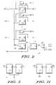
- FIG. 2illustrates a specific embodiment of a synchronous interface module 200 that can be used to implement the synchronous interface modules 1071 and 1161 of FIG. 1 .
- the synchronous interface module 200is illustrated to synchronize interrupt signals.
- the synchronous interface module 200includes synchronizers 211 - 214 , exclusive-or gates 221 - 223 (XORs 221 - 223 ), OR gate 231 , and clock gating module 240 .
- Synchronizer 211includes an input connected to receive a signal INT 0 , an output to provide a signal labeled INT 0 _s, and a clock input to receive a clock signal labeled CLK_g.
- Synchronizer 212includes an input connected to receive a signal INT 1 , an output to provide a signal labeled INT 1 _s, and a clock input to receive the clock signal labeled CLK_g.
- Synchronizer 213includes an input connected to receive a signal INT 2 , an output to provide a signal labeled INT 2 _s, and a clock input to receive a clock signal labeled CLK_g.
- XOR gate 221includes an input connected to the input of synchronizer 211 , an input connected to the output of the synchronizer 211 , and an output to provide a signal labeled DIFF 0 .
- XOR gate 222includes an input connected to the input of synchronizer 212 , an input connected to the output of the synchronizer 212 , and an output to provide a signal labeled DIFF 1 .
- XOR gate 223includes an input connected to the input of synchronizer 213 , an input connected to the output of the synchronizer 213 , and an output to provide a signal labeled DIFFn, where the suffix “n” represents an integer indicating the number of interrupt signals received at synchronous interface module 200 .
- OR gate 231includes n inputs, each respective input of OR gate 231 is connected to receive a corresponding signal of the signals DIFF 0 -DIFFn. OR gate 231 provides a signal labeled DIFF, which is asserted in response to any one of the signals DIFF 0 -DIFFn being asserted.
- Synchronizer 214includes an input connected to receive signal DIFF, an output to provide a signal labeled DIFF_s, and a clock input to receive a clock signal labeled CLK.
- Clock gating module 240includes an enable input connected to the output of synchronizer 214 to receive signal DIFF_s, an output to provide the signal labeled CLK_g, and an input labeled CK.
- FIG. 3illustrates a specific embodiment of a synchronizer 310 that can be used to implement the synchronizers 211 - 214 of FIG. 2 .
- Synchronizer 310includes a flip-flop 311 and a flip-flop 312 .
- Flip-flop 311includes an input connected to an input labeled IN of the synchronizer 310 , an output, and a clock input connected to an input labeled CK of the synchronizer 310 .
- Flip-flop 312includes an input connected to the output of the flip-flop 311 , and an output connected to the output labeled OUT of synchronizer 310 , and a clock input connected to an input labeled CK of the synchronizer 310 . Operation of the synchronous interface module 200 using synchronizers of the type illustrated at FIG. 3 will be better understood with reference to FIGS. 4-6 .
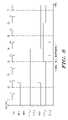
- FIG. 4illustrates a timing diagram illustrating the operation of the synchronous interface module 200 .
- FIG. 4illustrates a timing diagram illustrating the operation of the synchronous interface module 200 .
- timing traces labeled CLK, INT 0 , INT 1 , INT 0 _s, INT 1 _s, DIFF, DIFF_s, and CLK_gwhich correspond to commonly named signals of FIG. 2 .
- Signal CLKis a clock signal associated with the integrated circuit 101 .
- Seven clock periods P 0 -P 6are illustrated at FIG. 4 .
- Each respective clock period of FIG. 4is illustrated to begin at a corresponding time T 0 -T 6 , whereby a rising edge of signal CLK also corresponds to each of times T 0 -T 6 .
- clock period P 0begins at time T 0 of FIG. 4 .
- signals INT 0 and INT 1both have a logic low value (L). Note unless otherwise indicated, it is assumed that all other interrupts (INT 2 -INTn) of FIG. 2 are at a logic low value.
- the state of synchronous interface module 200 at time period P 0can represent a reset state of synchronous interface module 200 .
- Signal DIFFcan be referred to as an enable signal in that its logic value determines whether signal DIFF_s, which is provided to the enable input of clock gating module 240 , is asserted or negated to enable gating of signal CLK by clock gating module 240 .
- Negated signal DIFF at time period P 0is propagated to the output of Synchronizer 214 as negated signal DIFF_s at time period P 2 in response to synchronizing signal DIFF to signal CLK using the circuit of FIG. 2 .
- Negated signal DIFF_soperates as an enable signal that is received at the enable input of clock gating module 240 , thereby preventing signal CLK_g from transitioning in response to transitions of signal CLK during time period P 2 .
- signal INT 0changes logic state from a logic low value to a logic high value (H).
- the change in logic state at signal INT 0is asynchronous to signal CLK.
- the signal DIFF 0 at the output of XOR 221will be asserted at time period P 1 , thereby causing signal DIFF at the output of OR 231 to also be asserted during time period P 1 .
- signal DIFFremains asserted through time period P 3 .
- a change in logic state at INT 1 at period P 1would also result in signal DIFF being asserted in response to signal IN 1 having a different logic value than signal IN 1 _s.
- Asserted signal DIFF at time periods P 1 -P 3is propagated to the output of synchronizer 214 as asserted signal DIFF_s at time periods P 3 -P 5 in response to synchronizing signal DIFF to signal CLK.
- Asserted signal DIFF_sis received at the enable signal of clock gating module 240 at time periods P 3 -P 5 , thereby allowing clock gating module 240 to drive the signal CLK_g based upon the transitions of signal CLK so long as signal DIFF_s is asserted. Therefore, the clock input of the synchronizer 211 and the clock input of the synchronizer 212 are driven with seven transitions from time T 3 through time T 6 based upon transitions of signal CLK. Note that the number of transitions provided by clock gating module 240 are defined by implementation of the synchronous interface module 200 , and allow the synchronizer 211 and the synchronizer 212 to propagate signals at their inputs to their outputs.
- synchronizer 211propagates asserted signal INT 0 of time period P 1 as asserted signal INT 0 _s of time period P 3 in response to the rising transitions of signal CLK_g at times T 3 and T 4 . Since signal INT 0 _s is generated based upon the rising clock edges of signal CLK, signal INT 0 is referred to as being synchronized to signal CLK, and therefore can be provided in a deterministic manner to portions of integrated circuit 101 having the same time domain. For example, the interrupt module 116 of FIG. 1 can provide the synchronized signal INT 0 _s to the data processor 102 for handling.
- Negated signal DIFF_sis received at the enable input of clock gating module 240 , thereby preventing signal CLK_g, which is provided by clock gating module 240 and received at the clock inputs of synchronizer 211 and synchronizer 212 , from transitioning in response to transitions of signal CLK during time period P 4 .
- synchronization module 200reduces power consumption by driving the nodes connected to the inputs of synchronizers 211 and 212 in response to detecting a difference between a logic value at the input of a synchronizer and the output of the synchronizer.
- FIG. 5is a timing diagram illustrating timing traces corresponding to the same signals described at FIG. 4 .
- the state of the signals of time period P 0 of FIG. 5corresponds to the state of the signals of time period P 6 of FIG. 4 .
- Time period P 0 of FIG. 5can represent a time period immediately adjacent to time period P 6 of FIG. 4 .
- signal INT 0is negated, i.e., transitions from a logic high level to a logic low level.
- Signal INT 0can be negated by the source of the signal INT 0 in response to the interrupt being serviced, in response to the passing of a defined amount of time, and the like. Negation of the interrupt signal INT 0 at time period P 2 results in similar transitions of signal CLK_g as described with reference to assertion of signal INT 0 at FIG. 4 , thereby facilitating synchronization of signal INT 0 at FIG. 5 .
- FIG. 6is a timing diagram illustrating timing traces corresponding to the same signals described at FIG. 4 .
- the state of the signals of time period P 0 of FIG. 6corresponds to the state of the signals of time period P 6 of FIG. 4 .
- Time period P 0 of FIG. 6can represent a time period immediately adjacent to time period P 6 of FIG. 4 .
- signal INT 1is asserted.
- Signal INT 1is asynchronous to signal CLK, and as illustrated is also asynchronous to signal INT 0 , which may or may not change state in the same cycle as INT 1 , though it will be appreciated, that INT 1 can be either synchronous or asynchronous to signal INT 0 .
- FIG. 2illustrates a particular embodiment of a synchronous interface module that can reduce the amount of power needed to synchronize signals to a time domain identified with signal CLK, and that variations of the synchronous interface module of FIG. 2 are anticipated.
- FIG. 7illustrates an alternate embodiment of a synchronous interface module that can be used to implement synchronous interface modules of FIG. 1 .
- the synchronous interface module 600is illustrated to synchronize interrupts signals INT 0 -INTn for purposes of discussion.
- the synchronous interface module 600includes synchronizers 611 - 614 , exclusive-or gates 621 - 623 (XORs 621 - 623 ), OR gate 631 , control module 650 and clock gating module 640 .
- Synchronizers 611 - 614 , OR gates 621 - 623 , and OR gate 631are similarly connected to each other as corresponding elements of FIG. 2 , i.e., synchronizers 211 - 214 , OR gates 221 - 223 , and OR gate 231 , as previously described.
- Control module 650includes an input connected to the output of synchronizer 614 , an output, and a clock input connected to receive signal CLK.
- Clock gating module 640includes an enable input connected to the output of control module 650 , an output to provide the signal CLK_g, and an input to receive the signal CLK.
- the control module 650communicates with the clock gating module 640 to control the transitions of signal CLK_g differently than synchronous interface module 200 .
- the control module 650can allow for a different number of pulses to be generated at signal CLK_g during operation.
- the timing diagram of FIG. 4indicates that synchronous interface module 200 will generate a defined number of eight transitions at CLK_g in response to a difference between the input and the output of a synchronizer being held for at least three rising edges.
- Control module 650can be used to limit the transitions of CLK_g to only four transitions.
- FIG. 8illustrates assertion of signals CLK, INT 0 , and INT 1 in the same manner described at FIG. 4 , but results in four transitions, instead of eight, based upon a specific implementation of the control module 650 FIG. 7 , thereby reducing power consumption by reducing the number of times signal CLK_g transitions.
- FIG. 9illustrates a synchronous interface module 700 that is an alternate implementation of a synchronous interface module.
- Synchronization module 700includes synchronizers 711 - 714 , exclusive-or gates 721 - 723 (XORs 721 - 723 ), OR gate 731 , control module 750 and clock gating module 740 .
- a specific embodiment of synchronizers 711 - 714 of FIG. 7is illustrated in greater detail at FIG. 11 .
- Synchronizer 320 of FIG. 11includes a flip-flop 321 and a flip-flop 322 .
- Flip-flop 321includes an input connected to an input labeled IN of the synchronizer 320 , an output, a clock input connected to an input labeled CK 0 of the synchronizer 320 , and a clock input connected to an input labeled CK 1 of the synchronizer 320 .
- Flip-flop 322includes an input connected to the output of the flip-flop 321 , and an output connected to the output labeled OUT of synchronizer 320 , a clock input connected to an input labeled CK 1 of the synchronizer 320 .
- Synchronizers 711 - 714 , OR gates 721 - 723 , OR gate 731 , and control module 750are similarly connected to each other as corresponding elements of FIG. 6 , i.e., synchronizers 611 - 614 , OR gates 621 - 623 , OR gate 631 , and control module 750 as previously described.
- the signal DIFF_EN of control module 750includes two separate enable signals, DIFF 0 _EN and DIFF 1 _EN.
- Clock gating module 740includes AND gate 741 and AND gate 742 .
- One of the enable signals from control module 750is provided to a first input of AND gate 741 , and the other enable signal from control module 750 is provided to a first input of AND gate 742 .
- the signal CLKis provided to a second input of AND gate 741 , and to a second input of AND gate 742 .
- AND gate 741provides a signal CLK 1 _g, while AND gate 742 provides signal CLK 2 _g.
- control module 750controls clock gating module 740 in such a manner to provide a single pulse to clock input CLK 0 of synchronizers 711 - 713 , followed by a single pulse to clock input CLK 1 of synchronizers 711 - 713 to synchronize the interrupts signal INT 0 -INTn to signal CLK.
- FIG. 10illustrates assertion of signals CLK, INT 0 , and INT 1 in the same manner described at FIG. 4 , but resulting in four transitions, instead of six, based upon a specific implementation of FIG. 9 , thereby reducing power consumption by reducing the number of times signals CLK 0 _g and CLK 1 _g transition.
- FIG. 12illustrates a clock gating module 1200 that can represent the clock gating module 240 of FIG. 2 .
- the clock gating module 1200includes a transparent latch 1211 , an inverter 1212 , and an AND gate 1213 .
- the transparent latch 1211includes an enable input, a data input to receive the signal DIFF_s, and an output.
- the inverterincludes an input to receive the signal CLK, and an output connected to the enable input of the transparent latch 1211 .
- the AND gateincludes an input connected to the output of the transparent latch 1211 , an input to receive the signal CLK, and an output to provide the signal CLK_g.
- FIG. 13illustrates a timing diagram representative of the operation of a the synchronization device of FIG. 2 when the clock gating module 1200 is used. Specifically, four pulses, i.e., eight signal transitions, on signal CLK_g occur that correspond to rising edges of signal CLK during time periods P 4 -P 7 .
- FIGS. 2-13 of the disclosurehave been described with respect to interrupt signals.
- FIGS. 14 and 15illustrate a specific embodiment of a synchronizer module 1181 that passes information between an external module 124 and the external interface module 118 of integrated device 101 .
- FIG. 14illustrates a specific embodiment of a synchronization module 1181 of FIG. 1 that can operate as a gray code FIFO, which increments and decrements pointers based upon gray code to store and retrieve information from the FIFO memory to pass information across time domain boundaries.
- a FIFO 801is used to pass information, DATAIN_R, from external module 124 to external interface module 181 as DATAIN_W, and a FIFO 802 used to pass information, DATAOUT_R from external interface module 181 to external module 124 as DATAOUT_W.
- Control signals CTLIN_R and CTLOUT_Ware represented in FIG.
- FIG. 15illustrates a specific embodiment of FIFO 802 that synchronizes outbound data packets from external interface module 802 to external module 124 .
- FIG. 15illustrates a specific embodiment of FIFO 802 having three control signals that interface with the external interface module 181 and three control signals that interface with the external module 124 .
- Signals WCLK, WINC and WFULLinterface with the external interface module 181
- signals RCLK, REMPTY, and RINCinterface with the external module 124 .
- FIFO 802includes synchronous interface modules 1401 and 1402 that can operate as described herein to synchronize and pass read and write pointers across time domain boundaries to facilitate passing information through the FIFO memory. For example, based upon an asserted signal WINC, and assuming the FIFO is not full, the FIFO write control module of FIG.
- the 14will store information DATAOUT_R at address WADR of the FIFO memory in response to an internal clock (CLK_INT), determine whether the FIFO is full, assert signal WFULL if the FIFO is full to prevent storing additional data at the FIFO, and increment a current write pointer, WPTR, that is passed to the read control FIFO via the synchronizer 1401 to update the location of the current write pointer.
- the size of the pointeris based upon the size of the FIFO MEMORY and can be a gray code pointer, whereby only one digit of the pointer changes for each increment or decrement of the FIFO.
- the FIFO read control modulewill retrieve information DATAOUT_W at address RADDR of the FIFO memory in response to an external clock CLK_EXT, assert signal REMPTY if the FIFO is empty, and decrement and pass the current read pointer, RPTR, that is passed to the FIFO write controller via the synchronizer 1402 to update the location of the current read pointer.
- a second FIFOsimilar to the FIFO of FIG. 15 can be used to pass data from the external module 124 , e.g. DATAIN_R, to the external interface module 118 , e.g., DATAOUT_R.
Landscapes
- Engineering & Computer Science (AREA)
- Theoretical Computer Science (AREA)
- Physics & Mathematics (AREA)
- General Engineering & Computer Science (AREA)
- General Physics & Mathematics (AREA)
- Information Transfer Systems (AREA)
Abstract
Description
Claims (18)
Priority Applications (1)
| Application Number | Priority Date | Filing Date | Title |
|---|---|---|---|
| US12/134,913US8363766B2 (en) | 2008-06-06 | 2008-06-06 | Device and method of synchronizing signals |
Applications Claiming Priority (1)
| Application Number | Priority Date | Filing Date | Title |
|---|---|---|---|
| US12/134,913US8363766B2 (en) | 2008-06-06 | 2008-06-06 | Device and method of synchronizing signals |
Publications (2)
| Publication Number | Publication Date |
|---|---|
| US20090304134A1 US20090304134A1 (en) | 2009-12-10 |
| US8363766B2true US8363766B2 (en) | 2013-01-29 |
Family
ID=41400314
Family Applications (1)
| Application Number | Title | Priority Date | Filing Date |
|---|---|---|---|
| US12/134,913Expired - Fee RelatedUS8363766B2 (en) | 2008-06-06 | 2008-06-06 | Device and method of synchronizing signals |
Country Status (1)
| Country | Link |
|---|---|
| US (1) | US8363766B2 (en) |
Cited By (1)
| Publication number | Priority date | Publication date | Assignee | Title |
|---|---|---|---|---|
| US20160363955A1 (en)* | 2015-06-15 | 2016-12-15 | University Of Utah Research Foundation | Clock gating with an asynchronous wrapper cell |
Families Citing this family (4)
| Publication number | Priority date | Publication date | Assignee | Title |
|---|---|---|---|---|
| US20140203850A1 (en)* | 2013-01-24 | 2014-07-24 | Apple Inc. | Power managed synchronizers for asynchronous input signals |
| US11249511B2 (en)* | 2019-06-28 | 2022-02-15 | Intel Corporation | High performance clock domain crossing FIFO |
| CN112148655B (en)* | 2019-06-28 | 2023-11-17 | 深圳市中兴微电子技术有限公司 | Multi-bit data clock domain crossing processing method and device |
| CN113454723B (en)* | 2021-05-25 | 2024-08-16 | 长江存储科技有限责任公司 | Method and apparatus for power saving in semiconductor devices |
Citations (12)
| Publication number | Priority date | Publication date | Assignee | Title |
|---|---|---|---|---|
| US5649176A (en)* | 1995-08-10 | 1997-07-15 | Virtual Machine Works, Inc. | Transition analysis and circuit resynthesis method and device for digital circuit modeling |
| US5742546A (en) | 1994-09-12 | 1998-04-21 | Sgs-Thomson Microelectronics, S.A. | Method and device for address decoding in an integrated circuit memory |
| US5764966A (en)* | 1995-06-07 | 1998-06-09 | Samsung Electronics Co., Ltd. | Method and apparatus for reducing cumulative time delay in synchronizing transfer of buffered data between two mutually asynchronous buses |
| US6108352A (en)* | 1995-03-01 | 2000-08-22 | Intersil Corporation | Circuit and method for synchronizing outputs of two simultaneously transmitting devices in a multiplexed communication system |
| US6292044B1 (en)* | 1999-03-26 | 2001-09-18 | Lucent Technologies Inc. | Low power glitch-free clock switch |
| US20030076145A1 (en)* | 2001-10-19 | 2003-04-24 | Mitutoyo Corporation | Compact delay circuit for cmos integrated circuits used in low voltage low power devices |
| US20030210603A1 (en)* | 2002-05-08 | 2003-11-13 | Hui-Sian Ong | Method and apparatus for performing signal synchronization |
| US20040246810A1 (en)* | 2003-06-04 | 2004-12-09 | Dike Charles E. | Apparatus and method for reducing power consumption by a data synchronizer |
| US7250797B1 (en) | 2001-03-30 | 2007-07-31 | Agere Systems Inc. | Event edge synchronization system and method of operation thereof |
| US7288969B1 (en) | 2006-04-05 | 2007-10-30 | Alcatel Lucent | Zero clock delay metastability filtering circuit |
| US7436726B1 (en)* | 2005-11-21 | 2008-10-14 | Xilinx, Inc. | Circuit for and method of reading data in an asynchronous FIFO including a backup address circuit for re-reading data |
| US7551014B1 (en)* | 2007-02-01 | 2009-06-23 | Altera Corporation | Differential output with low output skew |
- 2008
- 2008-06-06USUS12/134,913patent/US8363766B2/ennot_activeExpired - Fee Related
Patent Citations (12)
| Publication number | Priority date | Publication date | Assignee | Title |
|---|---|---|---|---|
| US5742546A (en) | 1994-09-12 | 1998-04-21 | Sgs-Thomson Microelectronics, S.A. | Method and device for address decoding in an integrated circuit memory |
| US6108352A (en)* | 1995-03-01 | 2000-08-22 | Intersil Corporation | Circuit and method for synchronizing outputs of two simultaneously transmitting devices in a multiplexed communication system |
| US5764966A (en)* | 1995-06-07 | 1998-06-09 | Samsung Electronics Co., Ltd. | Method and apparatus for reducing cumulative time delay in synchronizing transfer of buffered data between two mutually asynchronous buses |
| US5649176A (en)* | 1995-08-10 | 1997-07-15 | Virtual Machine Works, Inc. | Transition analysis and circuit resynthesis method and device for digital circuit modeling |
| US6292044B1 (en)* | 1999-03-26 | 2001-09-18 | Lucent Technologies Inc. | Low power glitch-free clock switch |
| US7250797B1 (en) | 2001-03-30 | 2007-07-31 | Agere Systems Inc. | Event edge synchronization system and method of operation thereof |
| US20030076145A1 (en)* | 2001-10-19 | 2003-04-24 | Mitutoyo Corporation | Compact delay circuit for cmos integrated circuits used in low voltage low power devices |
| US20030210603A1 (en)* | 2002-05-08 | 2003-11-13 | Hui-Sian Ong | Method and apparatus for performing signal synchronization |
| US20040246810A1 (en)* | 2003-06-04 | 2004-12-09 | Dike Charles E. | Apparatus and method for reducing power consumption by a data synchronizer |
| US7436726B1 (en)* | 2005-11-21 | 2008-10-14 | Xilinx, Inc. | Circuit for and method of reading data in an asynchronous FIFO including a backup address circuit for re-reading data |
| US7288969B1 (en) | 2006-04-05 | 2007-10-30 | Alcatel Lucent | Zero clock delay metastability filtering circuit |
| US7551014B1 (en)* | 2007-02-01 | 2009-06-23 | Altera Corporation | Differential output with low output skew |
Non-Patent Citations (1)
| Title |
|---|
| Cummings, Clifford E., "Simulation and Synthesis Techniques for Asynchronous FIFO Design," Sunburst Design, Inc., SNUG San Jose 2002, Rev 12, pp. 1-23. |
Cited By (2)
| Publication number | Priority date | Publication date | Assignee | Title |
|---|---|---|---|---|
| US20160363955A1 (en)* | 2015-06-15 | 2016-12-15 | University Of Utah Research Foundation | Clock gating with an asynchronous wrapper cell |
| US9753486B2 (en)* | 2015-06-15 | 2017-09-05 | University Of Utah Research Foundation | Clock gating with an asynchronous wrapper cell |
Also Published As
| Publication number | Publication date |
|---|---|
| US20090304134A1 (en) | 2009-12-10 |
Similar Documents
| Publication | Publication Date | Title |
|---|---|---|
| US5506809A (en) | Predictive status flag generation in a first-in first-out (FIFO) memory device method and apparatus | |
| EP1293888B1 (en) | Methods and circuitry for implementing a first-in first-out structure | |
| US5920899A (en) | Asynchronous pipeline whose stages generate output request before latching data | |
| US6345328B1 (en) | Gear box for multiple clock domains | |
| JP5027241B2 (en) | High-speed serializer / deserializer transmission architecture | |
| US8001409B2 (en) | Synchronization device and methods thereof | |
| US7180332B2 (en) | Clock synchronization circuit | |
| CN101063894B (en) | Method and system for dynamically synchronizing processor clock and bus clock leading edge | |
| US7586337B2 (en) | Circuit for switching between two clock signals independently of the frequency of the clock signals | |
| US9330740B1 (en) | First-in first-out circuits and methods | |
| US8363766B2 (en) | Device and method of synchronizing signals | |
| US8493108B2 (en) | Synchronizer with high reliability | |
| US7242737B2 (en) | System and method for data phase realignment | |
| US20130007314A1 (en) | First in first out device and method thereof | |
| CN117769805A (en) | Aging reduction | |
| EP3739463B1 (en) | Circuit for asynchronous data transfer | |
| US8176352B2 (en) | Clock domain data transfer device and methods thereof | |
| US7392406B2 (en) | Circuit and method for generating clock signals for clocking digital signal processor and memory | |
| US6880050B1 (en) | Storage device, system and method which can use tag bits to synchronize queuing between two clock domains, and detect valid entries within the storage device | |
| US20050201163A1 (en) | Data synchronization arrangement | |
| US10742216B1 (en) | Clock domain crossing for an interface between logic circuits | |
| US7054205B2 (en) | Circuit and method for determining integrated circuit propagation delay | |
| US5249154A (en) | Data access controller and method | |
| JP2000353939A (en) | Clock signal synchronous flip flop circuit | |
| JP2002204448A (en) | Dot de-interleave circuit |
Legal Events
| Date | Code | Title | Description |
|---|---|---|---|
| AS | Assignment | Owner name:FREESCALE SEMICONDUCTOR, INC., TEXAS Free format text:ASSIGNMENT OF ASSIGNORS INTEREST;ASSIGNORS:AKERS, MATTHEW D.;SHAW, CRAIG D.;WALDROP, TIMOTHY K.;REEL/FRAME:021338/0652;SIGNING DATES FROM 20080623 TO 20080626 Owner name:FREESCALE SEMICONDUCTOR, INC., TEXAS Free format text:ASSIGNMENT OF ASSIGNORS INTEREST;ASSIGNORS:AKERS, MATTHEW D.;SHAW, CRAIG D.;WALDROP, TIMOTHY K.;SIGNING DATES FROM 20080623 TO 20080626;REEL/FRAME:021338/0652 | |
| AS | Assignment | Owner name:CITIBANK, N.A.,NEW YORK Free format text:SECURITY AGREEMENT;ASSIGNOR:FREESCALE SEMICONDUCTOR, INC.;REEL/FRAME:021570/0449 Effective date:20080728 Owner name:CITIBANK, N.A., NEW YORK Free format text:SECURITY AGREEMENT;ASSIGNOR:FREESCALE SEMICONDUCTOR, INC.;REEL/FRAME:021570/0449 Effective date:20080728 | |
| AS | Assignment | Owner name:CITIBANK, N.A.,NEW YORK Free format text:SECURITY AGREEMENT;ASSIGNOR:FREESCALE SEMICONDUCTOR, INC.;REEL/FRAME:024085/0001 Effective date:20100219 Owner name:CITIBANK, N.A., NEW YORK Free format text:SECURITY AGREEMENT;ASSIGNOR:FREESCALE SEMICONDUCTOR, INC.;REEL/FRAME:024085/0001 Effective date:20100219 | |
| AS | Assignment | Owner name:CITIBANK, N.A., AS COLLATERAL AGENT,NEW YORK Free format text:SECURITY AGREEMENT;ASSIGNOR:FREESCALE SEMICONDUCTOR, INC.;REEL/FRAME:024397/0001 Effective date:20100413 Owner name:CITIBANK, N.A., AS COLLATERAL AGENT, NEW YORK Free format text:SECURITY AGREEMENT;ASSIGNOR:FREESCALE SEMICONDUCTOR, INC.;REEL/FRAME:024397/0001 Effective date:20100413 | |
| FEPP | Fee payment procedure | Free format text:PAYOR NUMBER ASSIGNED (ORIGINAL EVENT CODE: ASPN); ENTITY STATUS OF PATENT OWNER: LARGE ENTITY | |
| STCF | Information on status: patent grant | Free format text:PATENTED CASE | |
| AS | Assignment | Owner name:CITIBANK, N.A., AS NOTES COLLATERAL AGENT, NEW YORK Free format text:SECURITY AGREEMENT;ASSIGNOR:FREESCALE SEMICONDUCTOR, INC.;REEL/FRAME:030633/0424 Effective date:20130521 Owner name:CITIBANK, N.A., AS NOTES COLLATERAL AGENT, NEW YOR Free format text:SECURITY AGREEMENT;ASSIGNOR:FREESCALE SEMICONDUCTOR, INC.;REEL/FRAME:030633/0424 Effective date:20130521 | |
| AS | Assignment | Owner name:CITIBANK, N.A., AS NOTES COLLATERAL AGENT, NEW YORK Free format text:SECURITY AGREEMENT;ASSIGNOR:FREESCALE SEMICONDUCTOR, INC.;REEL/FRAME:031591/0266 Effective date:20131101 Owner name:CITIBANK, N.A., AS NOTES COLLATERAL AGENT, NEW YOR Free format text:SECURITY AGREEMENT;ASSIGNOR:FREESCALE SEMICONDUCTOR, INC.;REEL/FRAME:031591/0266 Effective date:20131101 | |
| AS | Assignment | Owner name:FREESCALE SEMICONDUCTOR, INC., TEXAS Free format text:PATENT RELEASE;ASSIGNOR:CITIBANK, N.A., AS COLLATERAL AGENT;REEL/FRAME:037354/0719 Effective date:20151207 Owner name:FREESCALE SEMICONDUCTOR, INC., TEXAS Free format text:PATENT RELEASE;ASSIGNOR:CITIBANK, N.A., AS COLLATERAL AGENT;REEL/FRAME:037356/0143 Effective date:20151207 Owner name:FREESCALE SEMICONDUCTOR, INC., TEXAS Free format text:PATENT RELEASE;ASSIGNOR:CITIBANK, N.A., AS COLLATERAL AGENT;REEL/FRAME:037356/0553 Effective date:20151207 | |
| AS | Assignment | Owner name:MORGAN STANLEY SENIOR FUNDING, INC., MARYLAND Free format text:ASSIGNMENT AND ASSUMPTION OF SECURITY INTEREST IN PATENTS;ASSIGNOR:CITIBANK, N.A.;REEL/FRAME:037486/0517 Effective date:20151207 | |
| AS | Assignment | Owner name:MORGAN STANLEY SENIOR FUNDING, INC., MARYLAND Free format text:ASSIGNMENT AND ASSUMPTION OF SECURITY INTEREST IN PATENTS;ASSIGNOR:CITIBANK, N.A.;REEL/FRAME:037518/0292 Effective date:20151207 | |
| AS | Assignment | Owner name:MORGAN STANLEY SENIOR FUNDING, INC., MARYLAND Free format text:SECURITY AGREEMENT SUPPLEMENT;ASSIGNOR:NXP B.V.;REEL/FRAME:038017/0058 Effective date:20160218 | |
| FPAY | Fee payment | Year of fee payment:4 | |
| AS | Assignment | Owner name:MORGAN STANLEY SENIOR FUNDING, INC., MARYLAND Free format text:SUPPLEMENT TO THE SECURITY AGREEMENT;ASSIGNOR:FREESCALE SEMICONDUCTOR, INC.;REEL/FRAME:039138/0001 Effective date:20160525 | |
| AS | Assignment | Owner name:MORGAN STANLEY SENIOR FUNDING, INC., MARYLAND Free format text:CORRECTIVE ASSIGNMENT TO CORRECT THE REMOVE APPLICATION 12092129 PREVIOUSLY RECORDED ON REEL 038017 FRAME 0058. ASSIGNOR(S) HEREBY CONFIRMS THE SECURITY AGREEMENT SUPPLEMENT;ASSIGNOR:NXP B.V.;REEL/FRAME:039361/0212 Effective date:20160218 | |
| AS | Assignment | Owner name:NXP, B.V., F/K/A FREESCALE SEMICONDUCTOR, INC., NETHERLANDS Free format text:RELEASE BY SECURED PARTY;ASSIGNOR:MORGAN STANLEY SENIOR FUNDING, INC.;REEL/FRAME:040925/0001 Effective date:20160912 Owner name:NXP, B.V., F/K/A FREESCALE SEMICONDUCTOR, INC., NE Free format text:RELEASE BY SECURED PARTY;ASSIGNOR:MORGAN STANLEY SENIOR FUNDING, INC.;REEL/FRAME:040925/0001 Effective date:20160912 | |
| AS | Assignment | Owner name:NXP B.V., NETHERLANDS Free format text:RELEASE BY SECURED PARTY;ASSIGNOR:MORGAN STANLEY SENIOR FUNDING, INC.;REEL/FRAME:040928/0001 Effective date:20160622 | |
| AS | Assignment | Owner name:NXP USA, INC., TEXAS Free format text:MERGER;ASSIGNOR:FREESCALE SEMICONDUCTOR, INC.;REEL/FRAME:041144/0363 Effective date:20161107 | |
| AS | Assignment | Owner name:MORGAN STANLEY SENIOR FUNDING, INC., MARYLAND Free format text:CORRECTIVE ASSIGNMENT TO CORRECT THE REMOVE PATENTS 8108266 AND 8062324 AND REPLACE THEM WITH 6108266 AND 8060324 PREVIOUSLY RECORDED ON REEL 037518 FRAME 0292. ASSIGNOR(S) HEREBY CONFIRMS THE ASSIGNMENT AND ASSUMPTION OF SECURITY INTEREST IN PATENTS;ASSIGNOR:CITIBANK, N.A.;REEL/FRAME:041703/0536 Effective date:20151207 | |
| AS | Assignment | Owner name:MORGAN STANLEY SENIOR FUNDING, INC., MARYLAND Free format text:CORRECTIVE ASSIGNMENT TO CORRECT THE REMOVE APPLICATION 12681366 PREVIOUSLY RECORDED ON REEL 039361 FRAME 0212. ASSIGNOR(S) HEREBY CONFIRMS THE SECURITY AGREEMENT SUPPLEMENT;ASSIGNOR:NXP B.V.;REEL/FRAME:042762/0145 Effective date:20160218 Owner name:MORGAN STANLEY SENIOR FUNDING, INC., MARYLAND Free format text:CORRECTIVE ASSIGNMENT TO CORRECT THE REMOVE APPLICATION 12681366 PREVIOUSLY RECORDED ON REEL 038017 FRAME 0058. ASSIGNOR(S) HEREBY CONFIRMS THE SECURITY AGREEMENT SUPPLEMENT;ASSIGNOR:NXP B.V.;REEL/FRAME:042985/0001 Effective date:20160218 | |
| AS | Assignment | Owner name:SHENZHEN XINGUODU TECHNOLOGY CO., LTD., CHINA Free format text:CORRECTIVE ASSIGNMENT TO CORRECT THE TO CORRECT THE APPLICATION NO. FROM 13,883,290 TO 13,833,290 PREVIOUSLY RECORDED ON REEL 041703 FRAME 0536. ASSIGNOR(S) HEREBY CONFIRMS THE THE ASSIGNMENT AND ASSUMPTION OF SECURITYINTEREST IN PATENTS.;ASSIGNOR:MORGAN STANLEY SENIOR FUNDING, INC.;REEL/FRAME:048734/0001 Effective date:20190217 | |
| AS | Assignment | Owner name:NXP B.V., NETHERLANDS Free format text:RELEASE BY SECURED PARTY;ASSIGNOR:MORGAN STANLEY SENIOR FUNDING, INC.;REEL/FRAME:050744/0097 Effective date:20190903 Owner name:NXP B.V., NETHERLANDS Free format text:RELEASE BY SECURED PARTY;ASSIGNOR:MORGAN STANLEY SENIOR FUNDING, INC.;REEL/FRAME:050745/0001 Effective date:20190903 | |
| AS | Assignment | Owner name:MORGAN STANLEY SENIOR FUNDING, INC., MARYLAND Free format text:CORRECTIVE ASSIGNMENT TO CORRECT THE REMOVE APPLICATION 12298143 PREVIOUSLY RECORDED ON REEL 042985 FRAME 0001. ASSIGNOR(S) HEREBY CONFIRMS THE SECURITY AGREEMENT SUPPLEMENT;ASSIGNOR:NXP B.V.;REEL/FRAME:051029/0001 Effective date:20160218 Owner name:MORGAN STANLEY SENIOR FUNDING, INC., MARYLAND Free format text:CORRECTIVE ASSIGNMENT TO CORRECT THE REMOVE APPLICATION 12298143 PREVIOUSLY RECORDED ON REEL 042762 FRAME 0145. ASSIGNOR(S) HEREBY CONFIRMS THE SECURITY AGREEMENT SUPPLEMENT;ASSIGNOR:NXP B.V.;REEL/FRAME:051145/0184 Effective date:20160218 Owner name:MORGAN STANLEY SENIOR FUNDING, INC., MARYLAND Free format text:CORRECTIVE ASSIGNMENT TO CORRECT THE REMOVE APPLICATION 12298143 PREVIOUSLY RECORDED ON REEL 039361 FRAME 0212. ASSIGNOR(S) HEREBY CONFIRMS THE SECURITY AGREEMENT SUPPLEMENT;ASSIGNOR:NXP B.V.;REEL/FRAME:051029/0387 Effective date:20160218 Owner name:MORGAN STANLEY SENIOR FUNDING, INC., MARYLAND Free format text:CORRECTIVE ASSIGNMENT TO CORRECT THE REMOVE APPLICATION12298143 PREVIOUSLY RECORDED ON REEL 039361 FRAME 0212. ASSIGNOR(S) HEREBY CONFIRMS THE SECURITY AGREEMENT SUPPLEMENT;ASSIGNOR:NXP B.V.;REEL/FRAME:051029/0387 Effective date:20160218 Owner name:MORGAN STANLEY SENIOR FUNDING, INC., MARYLAND Free format text:CORRECTIVE ASSIGNMENT TO CORRECT THE REMOVE APPLICATION 12298143 PREVIOUSLY RECORDED ON REEL 038017 FRAME 0058. ASSIGNOR(S) HEREBY CONFIRMS THE SECURITY AGREEMENT SUPPLEMENT;ASSIGNOR:NXP B.V.;REEL/FRAME:051030/0001 Effective date:20160218 Owner name:MORGAN STANLEY SENIOR FUNDING, INC., MARYLAND Free format text:CORRECTIVE ASSIGNMENT TO CORRECT THE REMOVE APPLICATION12298143 PREVIOUSLY RECORDED ON REEL 042985 FRAME 0001. ASSIGNOR(S) HEREBY CONFIRMS THE SECURITY AGREEMENT SUPPLEMENT;ASSIGNOR:NXP B.V.;REEL/FRAME:051029/0001 Effective date:20160218 Owner name:MORGAN STANLEY SENIOR FUNDING, INC., MARYLAND Free format text:CORRECTIVE ASSIGNMENT TO CORRECT THE REMOVE APPLICATION12298143 PREVIOUSLY RECORDED ON REEL 042762 FRAME 0145. ASSIGNOR(S) HEREBY CONFIRMS THE SECURITY AGREEMENT SUPPLEMENT;ASSIGNOR:NXP B.V.;REEL/FRAME:051145/0184 Effective date:20160218 | |
| AS | Assignment | Owner name:MORGAN STANLEY SENIOR FUNDING, INC., MARYLAND Free format text:CORRECTIVE ASSIGNMENT TO CORRECT THE REMOVE APPLICATION11759915 AND REPLACE IT WITH APPLICATION 11759935 PREVIOUSLY RECORDED ON REEL 037486 FRAME 0517. ASSIGNOR(S) HEREBY CONFIRMS THE ASSIGNMENT AND ASSUMPTION OF SECURITYINTEREST IN PATENTS;ASSIGNOR:CITIBANK, N.A.;REEL/FRAME:053547/0421 Effective date:20151207 | |
| AS | Assignment | Owner name:NXP B.V., NETHERLANDS Free format text:CORRECTIVE ASSIGNMENT TO CORRECT THE REMOVEAPPLICATION 11759915 AND REPLACE IT WITH APPLICATION11759935 PREVIOUSLY RECORDED ON REEL 040928 FRAME 0001. ASSIGNOR(S) HEREBY CONFIRMS THE RELEASE OF SECURITYINTEREST;ASSIGNOR:MORGAN STANLEY SENIOR FUNDING, INC.;REEL/FRAME:052915/0001 Effective date:20160622 | |
| AS | Assignment | Owner name:NXP, B.V. F/K/A FREESCALE SEMICONDUCTOR, INC., NETHERLANDS Free format text:CORRECTIVE ASSIGNMENT TO CORRECT THE REMOVEAPPLICATION 11759915 AND REPLACE IT WITH APPLICATION11759935 PREVIOUSLY RECORDED ON REEL 040925 FRAME 0001. ASSIGNOR(S) HEREBY CONFIRMS THE RELEASE OF SECURITYINTEREST;ASSIGNOR:MORGAN STANLEY SENIOR FUNDING, INC.;REEL/FRAME:052917/0001 Effective date:20160912 | |
| FEPP | Fee payment procedure | Free format text:MAINTENANCE FEE REMINDER MAILED (ORIGINAL EVENT CODE: REM.); ENTITY STATUS OF PATENT OWNER: LARGE ENTITY | |
| LAPS | Lapse for failure to pay maintenance fees | Free format text:PATENT EXPIRED FOR FAILURE TO PAY MAINTENANCE FEES (ORIGINAL EVENT CODE: EXP.); ENTITY STATUS OF PATENT OWNER: LARGE ENTITY | |
| STCH | Information on status: patent discontinuation | Free format text:PATENT EXPIRED DUE TO NONPAYMENT OF MAINTENANCE FEES UNDER 37 CFR 1.362 | |
| FP | Lapsed due to failure to pay maintenance fee | Effective date:20210129 |