US8362833B2 - Amplifier circuitry, integrated circuit and communication unit - Google Patents
Amplifier circuitry, integrated circuit and communication unitDownload PDFInfo
- Publication number
- US8362833B2 US8362833B2US13/131,039US200913131039AUS8362833B2US 8362833 B2US8362833 B2US 8362833B2US 200913131039 AUS200913131039 AUS 200913131039AUS 8362833 B2US8362833 B2US 8362833B2
- Authority
- US
- United States
- Prior art keywords
- amplifier circuitry
- signal
- modulation logic
- sigma
- logic
- Prior art date
- Legal status (The legal status is an assumption and is not a legal conclusion. Google has not performed a legal analysis and makes no representation as to the accuracy of the status listed.)
- Expired - Fee Related
Links
Images


Classifications
- H—ELECTRICITY
- H03—ELECTRONIC CIRCUITRY
- H03F—AMPLIFIERS
- H03F3/00—Amplifiers with only discharge tubes or only semiconductor devices as amplifying elements
- H03F3/20—Power amplifiers, e.g. Class B amplifiers, Class C amplifiers
- H03F3/21—Power amplifiers, e.g. Class B amplifiers, Class C amplifiers with semiconductor devices only
- H03F3/217—Class D power amplifiers; Switching amplifiers
- H03F3/2173—Class D power amplifiers; Switching amplifiers of the bridge type
- H—ELECTRICITY
- H03—ELECTRONIC CIRCUITRY
- H03F—AMPLIFIERS
- H03F1/00—Details of amplifiers with only discharge tubes, only semiconductor devices or only unspecified devices as amplifying elements
- H03F1/02—Modifications of amplifiers to raise the efficiency, e.g. gliding Class A stages, use of an auxiliary oscillation
- H03F1/0205—Modifications of amplifiers to raise the efficiency, e.g. gliding Class A stages, use of an auxiliary oscillation in transistor amplifiers
- H—ELECTRICITY
- H03—ELECTRONIC CIRCUITRY
- H03F—AMPLIFIERS
- H03F1/00—Details of amplifiers with only discharge tubes, only semiconductor devices or only unspecified devices as amplifying elements
- H03F1/30—Modifications of amplifiers to reduce influence of variations of temperature or supply voltage or other physical parameters
- H03F1/303—Modifications of amplifiers to reduce influence of variations of temperature or supply voltage or other physical parameters using a switching device
- H03F1/304—Modifications of amplifiers to reduce influence of variations of temperature or supply voltage or other physical parameters using a switching device and using digital means
- H—ELECTRICITY
- H03—ELECTRONIC CIRCUITRY
- H03F—AMPLIFIERS
- H03F3/00—Amplifiers with only discharge tubes or only semiconductor devices as amplifying elements
- H03F3/20—Power amplifiers, e.g. Class B amplifiers, Class C amplifiers
- H03F3/21—Power amplifiers, e.g. Class B amplifiers, Class C amplifiers with semiconductor devices only
- H03F3/217—Class D power amplifiers; Switching amplifiers
- H—ELECTRICITY
- H03—ELECTRONIC CIRCUITRY
- H03F—AMPLIFIERS
- H03F2200/00—Indexing scheme relating to amplifiers
- H03F2200/03—Indexing scheme relating to amplifiers the amplifier being designed for audio applications
- H—ELECTRICITY
- H03—ELECTRONIC CIRCUITRY
- H03F—AMPLIFIERS
- H03F2200/00—Indexing scheme relating to amplifiers
- H03F2200/331—Sigma delta modulation being used in an amplifying circuit
- H—ELECTRICITY
- H03—ELECTRONIC CIRCUITRY
- H03F—AMPLIFIERS
- H03F2200/00—Indexing scheme relating to amplifiers
- H03F2200/453—Controlling being realised by adding a replica circuit or by using one among multiple identical circuits as a replica circuit
- H—ELECTRICITY
- H03—ELECTRONIC CIRCUITRY
- H03F—AMPLIFIERS
- H03F2200/00—Indexing scheme relating to amplifiers
- H03F2200/459—Ripple reduction circuitry being used in an amplifying circuit
Definitions
- the field of this inventionrelates to amplifier circuitry, and in particular to amplifier circuitry for amplifying an audio input signal and an integrated circuit and communication unit comprising said amplifier circuitry.
- an audio outputtypically requires a low impedance speaker and a performance audio amplifier.
- these elementsare selected to achieve high power efficiency in order to minimise power consumption, and thereby improve battery life.
- Class-D amplifierswhich use switching modes of transistors to regulate power delivery, are good candidates, and thus are typically used for such audio applications.
- FIG. 1illustrates an example of a conventional Sigma-Delta based class-D amplifier 100 .
- the amplifier 100comprises PDM (Pulse Density Modulation) Sigma-Delta modulator circuitry 110 , operably coupled to a low distortion power driver 120 , which in turn is operably coupled to a speaker 130 .
- PDMPulse Density Modulation
- Such a conventional amplifier arrangementcomprises good total harmonic distortion and noise (THD+N) characteristics, a good power supply rejection ratio (PSSR), and good immunity to electromagnetic interference (EMI).
- TDD+Ntotal harmonic distortion and noise
- PSSRgood power supply rejection ratio
- EMIimmunity to electromagnetic interference
- FIG. 2illustrates a graphical example 200 of the output power spectrum against frequency for the amplifier 100 of FIG. 1 .
- the impedance 210 of speaker 130is low. Accordingly, the majority of the power spectrum at these frequencies comprises the active power (audio signal).
- the speaker 130due to its inductance model, naturally performs low-pass filtering of the received signal in the analogue domain and removes part of the quantization noise and signal image. Accordingly, at higher frequencies, the impedance of the speaker 130 increases. In particular, at frequencies corresponding to the shaped quantization noise and signal image, the impedance of the speaker 130 is significant, resulting in significant power attenuation at these higher frequencies.
- the power efficiency of amplifier 100may be defined as:
- Vout audio 2 Zspk audiorepresents the active power (audio signal);
- Vout HF 2 Zspk HFrepresents the high frequency (HF) power attenuation (sigma-delta modulation and signal image);
- Vout audio Zspk audio2 . represents the conductive power loss (ON resistance of power stage);
- Vbat 2 ⁇ C par ⁇ frepresents the switching power loss
- Vaudio ⁇ Iccrepresents the bias power loss (class-D internal consumption).
- the higher frequency power attenuationis particularly significant for low level input signals, where the quantization noise becomes proportionately large. Consequently, the power efficiency of the conventional amplifier circuitry 100 of FIG. 1 for low level input signals is dependent, to a large extent, on the speaker impedance at these higher frequencies. Accordingly, the speaker impedance characteristics are a considerable contributor to power efficiency loss of the amplifier circuitry 100 , and as such the power efficiency loss can vary from speaker to speaker.
- the kind of audio architecture illustrated in FIG. 1may require an external LC filter to improve the power efficiency during low level input signals. Consequently, the choice of speakers that might be suitable for use within an audio enabled device using such a conventional amplifier is limited by the impedance of the speakers, irrespective of any other beneficial or desirable features that the speakers may have.
- the present inventionprovides amplifier circuitry, a semiconductor device and a communication unit as described in the accompanying claims.
- FIG. 1illustrates an example of a conventional Sigma-Delta based class-D amplifier.
- FIG. 2illustrates an example of the output power spectrum against frequency for the amplifier of FIG. 1 .
- FIG. 3illustrates an example of a block diagram of part of a communication unit.
- FIG. 4illustrates an example of an integrated circuit comprising an example of amplifier circuitry.
- FIG. 5illustrates an alternative example of an amplifier circuit.
- FIG. 6illustrates further alternative example of amplifier circuit.
- FIG. 7illustrates a still further example of an alternative amplifier circuit.
- FIG. 8illustrates a graphical example showing a power spectrum against frequency for the amplifier circuitry of FIG. 4 .
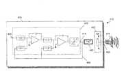
- the communication unit 300in the context of this example, is a mobile telephone handset comprising an antenna 302 .
- the communication unit 300contains a variety of well known radio frequency components or circuits 306 , operably coupled to the antenna 302 that will not be described further herein.
- the communication unit 300further comprises signal processing logic 308 .
- An output from the signal processing logic 308is provided to a suitable user interface (UI) 310 comprising, for example, a display, keypad, etc.
- UIuser interface
- the user interface 310comprises amplifier circuitry 312 operably coupled to a speaker 314 .
- the signal processing logic 308is coupled to a memory element 316 that stores operating regimes, such as decoding/encoding functions and the like and may be realised in a variety of technologies such as random access memory (RAM) (volatile), (non-volatile) read only memory (ROM), Flash memory or any combination of these or other memory technologies.
- a timer 318is typically coupled to the signal processing logic 308 to control the timing of operations within the communication unit 300 .
- the amplifier circuitry 312is arranged to amplify an audio input signal 420 and comprises modulation logic 410 .
- the modulation logic 410is arranged to receive the audio input signal 420 and to generate a modulated signal 415 that is representative of the audio input signal 420 .
- the amplifier circuitry 312further comprises an output stage 430 arranged to generate an output signal 435 for the amplifier circuitry 312 based on the modulated signal 415 .
- the amplifier circuitry 312is arranged to be operably coupled to a load, which for the illustrated example is in the form of speaker 314 .
- the impedance of speakersis typically low. Accordingly, the majority of a power spectrum for the output of the speaker 314 at these frequencies comprises the active power (wanted audio signal).
- the speaker 314low-pass filters the received signal in the analogue domain and removes part of the quantization noise, signal image etc. Accordingly, at higher frequencies the impedance of the speaker 314 increases, and in particular at frequencies corresponding to shaped quantization noise and signal image, the impedance of the speaker 314 is significant, resulting in significant power attenuation at these higher frequencies. This higher frequency power attenuation is particularly significant for low level input signals, where the quantization noise becomes proportionately large.
- the amplifier circuitry 312further comprises a filter 450 operably coupled between the modulation logic 410 and the output stage 430 .
- the filter 450is arranged to substantially pass signal components within the modulated signal 415 that represent wanted audio frequencies, and to attenuate signal components within the modulated signal 415 that represent higher frequencies comprising quantization noise.
- the filter 450may be arranged to attenuate signal components within the modulated signal 415 that represent frequencies substantially in a region of half a switching frequency of the modulation logic 410 .
- the filter 450reduces the power spectral density of the output signal 435 at frequencies substantially in the region of half the switching frequency of the modulation logic 410 .
- quantization noise located in the region of half the switching frequency of the modulation logic 410may be substantially reduced/filtered out by filter 450 .
- quantization noiseis attenuated prior to the output stage 430 , thereby generating the amplified output signal 435 .
- the speaker 314performs one further order of filtering of the amplified quantization noise, further reducing the associated power loss. This reduction in power loss, and corresponding increase in efficiency, is particularly significant for low level input signals.
- the filter 450comprises finite impulse response (FIR) filter logic, and in particular (1+z ⁇ k ) FIR filter logic, where k represents the order of the filter.
- FIRfinite impulse response
- IIRInfinite Impulse Response
- FIR filter logicsuch as that illustrated in FIG. 4 , provides a benefit of being simple to implement using digital delays.
- the filter 450may comprise a digital delay component in a form of a flip-flop.
- FIG. 8there is illustrated a graphical example of the output power spectrum against frequency 800 for the amplifier circuitry 312 of FIG. 4 , as well as a graphical example of a transfer function 830 for filter 450 of FIG. 4 .
- a wanted, audio frequency component 810 of the output power spectrumis located at a lower frequency range within the power spectrum 800 of the amplifier circuitry 312 , substantially adjacent zero hertz, or DC (Direct Current) 815 for the illustrated example.
- the modulation logic 410 of FIG. 4is a discrete time circuit arranged to operate at a switching frequency f s 825 .
- an image of the audio frequency component 820is produced by the modulation logic 410 which is substantially symmetrical to the wanted audio frequency component 810 and arranged to be about half the switching frequency (f s /2) 835 (Nyquist criteria).
- the filter 450 for the illustrated exampleis arranged to operate at the same clock speed as the modulation logic 410 , namely at the switching frequency f s 825 . Accordingly, the filter 450 is subject to the same symmetrical characteristics about f s /2 835 . As a result, if the filter 450 were arranged to attenuate the image of the audio frequency component 820 , substantially symmetrical attenuation would occur about f s /2 835 , thereby causing the wanted, audio frequency component 810 to also be attenuated.
- the filter 450is arranged to attenuate signal components within the modulated signal ( 415 ) that represents frequencies substantially in the region of half the switching frequency (f s /2) 835 of the modulation logic 410 , whilst passing signal components within the modulated signal 415 that represents wanted audio frequencies 810 .
- the transfer function of the filter logic 410comprises a single zero, and in particular comprises a single zero arranged to be substantially located at half the switching frequency (f s /2) 835 .
- unwanted componentssuch as quantization noise that were present in the region of half the switching frequency (f s /2) 835 may be attenuated.
- unwanted componentsmay be attenuated out of the modulated signal 415 within the digital domain, prior to the output stage 430 generating the amplified output signal 435 . Consequently, the speaker 314 performs one further order of filtering of the amplified quantization noise, further reducing the associated power loss.
- the (1+z k ) FIR filter logic 410may comprise a transfer function with more than one zero substantially equally distributed between zero, so long as the zeros are hertz (DC) and the switching frequency of the modulation logic 410 , and in particular within the region of half the switching frequency of the modulation logic ( 410 ).
- the amplifier circuitry 312comprises a switching mode amplifier, and in particular a class-D amplifier.
- Such amplifiersprovide the benefit of high power efficiency (low energy losses), as well as reduced size and weight due to their not requiring bulky heat sinks and the like.
- the modulation logic 410 illustrated in FIG. 4is arranged to perform pulsed density modulation to generate the modulated signal 415 , and may for example comprise Sigma-Delta modulation logic.
- the modulation logic 410may be arranged to shape quantization noise such that the quantization noise, is substantially concentrated at frequencies in the region of half the switching frequency of the modulation logic 410 . In this manner, a larger proportion of the quantization noise may be attenuated by the filter logic 450 .
- the amplifier circuitry 312comprises a feedback loop 460 arranged to provide feedback to the modulation logic 410 .
- the feedback loop 460is arranged to provide feedback from the modulated signal 415 generated by the modulation logic 410 , which is fed back in to the modulation logic 410 , enabling the modulation logic 410 to shape the quantization noise.
- the amplifier circuitry 312comprises no output stage feedback.
- the modulation logic 410is not able to take into account, and thus not compensate for, power supply noise introduced by the output stage 430 . Consequently, the amplifier circuitry 312 may be susceptible to a poor Power Supply Rejection Ratio (PSRR) from the output stage 430 as a result of a potentially noisy power supply.
- PSRRPower Supply Rejection Ratio
- the amplifier circuitry 312 of FIG. 5comprises modulation logic 410 arranged to receive the audio input signal 420 and to generate a modulated signal 415 that is representative of the audio input signal 420 .
- the amplifier circuitry 312 of FIG. 5also comprises output stage 430 arranged to generate an output signal 435 for the amplifier circuitry 312 based on the modulated signal 415 , and filter 450 operably coupled between the modulation 410 and the output stage 430 .
- the amplifier circuitry 312comprises a feedback loop 570 arranged to provide feedback to the modulation logic 410 from the output signal 435 generated by the output stage 430 .
- the modulation logic 410is able to take into account, and compensate for, power supply noise introduced by the output stage 430 .
- the amplifier circuitry 312 of FIG. 5is capable of a good PSSR performance.
- the feedback loop 570provides feedback to the modulation logic 410 from the output signal 435 generated by the output stage 430 .
- the feedbackcomprises characteristics introduced by the filter 450 .
- the feedbackmay comprise one or more ‘zeros’ within its power spectrum that have been introduced by the attenuation of the filter 450 . Consequently, the modulation logic 410 may attempt to compensate for these zeros by creating additional poles within the quantization noise transfer function of the modulated signal 415 . As a result, the amount of quantization noise would be increased, saturating the modulation logic 410 , potentially resulting in the modulated logic 410 becoming unstable.
- FIG. 6illustrates a yet further alternative example of amplifier circuitry 312 .
- the amplifier circuitry 312 of FIG. 6comprises modulation logic 410 arranged to receive the audio input signal 420 and to generate a modulated signal 415 that is representative of the audio input signal 420 .
- the amplifier circuitry 312 of FIG. 5also comprises output stage 430 arranged to generate an output signal 435 for the amplifier circuitry 312 based on the modulated signal 415 , and filter logic 450 operably coupled between the modulation 410 and the output stage 430 .
- FIG. 6illustrates a yet further alternative example of amplifier circuitry 312 .
- the amplifier circuitry 312 of FIG. 6comprises modulation logic 410 arranged to receive the audio input signal 420 and to generate a modulated signal 415 that is representative of the audio input signal 420 .
- the amplifier circuitry 312 of FIG. 5also comprises output stage 430 arranged to generate an output signal 435 for the amplifier circuitry 312 based on the modulated signal 415 , and filter
- the amplifier circuitry 312comprises a first feedback loop 570 arranged to provide feedback to the modulation 410 from the output signal 435 generated by the output stage 430 .
- the modulation logic 410is able to at least partially take into account, and compensate for, power supply noise introduced by the output stage 430 .
- the amplifier circuitry 312 of FIG. 6further comprises a second feedback loop 660 arranged to provide feedback to the modulation logic 410 from the modulated signal 415 generated thereby.
- the second feedback loop 660provides feedback to the modulation logic 410 that is substantially free of characteristics introduced by the filter 450 .
- the effect of the attenuation of the filter 450 within the feedback provided to the modulation logic 410is reduced, and the modulation logic 410 remains stable.
- the modulation logic 410In order for the modulation logic 410 to perform k order shaping of noise, the noise to be shaped is required to be applied to ‘k’ feedback loops. For the example illustrated in FIG. 6 , the feedback from the output signal 435 is only applied to one of the feedback loops. As a result, the modulation logic 410 is only able to perform first order PSRR shaping.
- FIG. 7illustrates a still further alternative example of amplifier circuitry 312 .
- the amplifier circuitry 312comprises modulation logic 410 arranged to receive the audio input signal 420 and to generate a modulated signal 415 that is representative of the audio input signal 420 .
- the amplifier circuitry 312also comprises output stage 430 arranged to generate an output signal 435 for the amplifier circuitry 312 based on the modulated signal 415 , and filter 450 operably coupled between the modulation logic 410 and the output stage 430 .
- the amplifier circuitry 312comprises a first feedback loop 570 arranged to provide feedback to the modulation logic 410 from the output signal 435 generated by the output stage 430 .
- the modulation logic 410is able to perform first order PSRR shaping.
- the amplifier circuitry 312 of FIG. 7comprises a further feedback loop 760 arranged to provide feedback to the modulation logic 410 from the modulated signal 415 generated thereby.
- the further feedback loop 760comprises power supply representation logic 780 arranged to introduce a representation of power supply noise into the further feedback loop 760 .
- power supply noiseis applied to both feedback loops 570 , 660 , thereby enabling the modulation logic 410 to perform not just first order PSRR shaping but second order PSRR shaping as well.
- the power supply representation logic 780comprises mock power stage and load circuitry.
- the mock power stage and load circuitrycomprises a mock power stage 782 , for example having an ON impedance substantially ‘N’ times higher than the output stage 430 of the amplifier circuitry 312 , and a mock load 784 comprising an impedance substantially ‘N’ times higher than that of the load of the amplifier circuitry 312 , which for the illustrated embodiment is in the form of speaker 314 .
- the ‘N’ factor on the mock power stage and loadallows the integration of a copy of the power stage “N” times smaller in size than the main power stage and “N” times less power consuming.
- the modulation logic 410comprises a 2 nd order modulator.
- the amplifier circuitrymay comprise modulation logic 410 comprising an i th order modulator, where T may comprise a value other than two.
- the amplifier circuitry 312may comprise a first feedback loop, such as feedback loop 570 , arranged to provide feedback to the modulation logic 410 from the output signal 435 generated by the output stage 430 , and (i ⁇ 1) further feedback loops, such as feedback loop 760 , arranged to provide feedback to the modulation logic 410 from the modulated signal 415 generated thereby.
- the (i ⁇ 1) further feedback loopsmay comprise power supply representation logic, such as mock power stage and load circuitry 780 .
- connectionsmay be any type of connection suitable to transfer signals from or to the respective nodes, units or devices, for example via intermediate devices. Accordingly, unless implied or stated otherwise the connections may for example be direct connections or indirect connections.
- the conductors as discussed hereinmay be illustrated or described in reference to being a single conductor, a plurality of conductors, unidirectional conductors, or bidirectional conductors. However, different examples may vary the implementation of the conductors. For example, separate unidirectional conductors may be used rather than bidirectional conductors and vice versa. Also, plurality of conductors may be replaced with a single conductor that transfers multiple signals serially or in a time multiplexed manner. Likewise, single conductors carrying multiple signals may be separated out into various different conductors carrying subsets of these signals. Therefore, many options exist for transferring signals.
- any two components herein combined to achieve a particular functionalitycan be seen as “associated with” each other such that the desired functionality is achieved, irrespective of architectures or intermediary components.
- any two components so associatedcan also be viewed as being “operably connected,” or “operably coupled,” to each other to achieve the desired functionality.
- the inventionis not limited to physical devices or units implemented in non-programmable hardware but can also be applied in programmable devices or units able to perform the desired device functions by operating in accordance with suitable program code.
- the devicesmay be physically distributed over a number of apparatuses, while functionally operating as a single device.
- devices functionally forming separate devicesmay be integrated in a single physical device.
- any reference signs placed between parenthesesshall not be construed as limiting the claim.
- the word ‘comprising’does not exclude the presence of other elements or steps then those listed in a claim.
- the terms “a” or “an,” as used herein,are defined as one or more than one.
Landscapes
- Engineering & Computer Science (AREA)
- Power Engineering (AREA)
- Amplifiers (AREA)
Abstract
Description
where:
represents the active power (audio signal);
represents the high frequency (HF) power attenuation (sigma-delta modulation and signal image);
represents the conductive power loss (ON resistance of power stage);
- (i) reduced power loss leading to improved efficiency of audio arrangements, which in turn enables improved battery life for communication units;
- (ii) reduced power efficiency limitations that are typically inherent to the high frequency power spectral density of Sigma-Delta based class-D amplifiers;
- (iii) modulator stability within amplifier circuitry, due to feedback loop flexibility;
- (iv) maintaining good total harmonic distortion and noise (THD+N) characteristics, a good power supply rejection ratio (PSSR), and good immunity to electromagnetic interference (EMI);
- (v) alleviating the need for external components, such as external LC filters, for improving the power efficiency during low level input signals;
- (vi) a simple implementation based on digital delays;
- (vii) power efficiency being less sensitive to load (speaker) characteristics; and
- (viii) no significant impact on the die size or cost for the amplifier circuitry.
Claims (16)
Applications Claiming Priority (1)
| Application Number | Priority Date | Filing Date | Title |
|---|---|---|---|
| PCT/IB2009/051969WO2010076672A1 (en) | 2009-01-05 | 2009-01-05 | Amplifier circuitry, integrated circuit and communication unit |
Publications (2)
| Publication Number | Publication Date |
|---|---|
| US20110248779A1 US20110248779A1 (en) | 2011-10-13 |
| US8362833B2true US8362833B2 (en) | 2013-01-29 |
Family
ID=41076687
Family Applications (1)
| Application Number | Title | Priority Date | Filing Date |
|---|---|---|---|
| US13/131,039Expired - Fee RelatedUS8362833B2 (en) | 2009-01-05 | 2009-01-05 | Amplifier circuitry, integrated circuit and communication unit |
Country Status (2)
| Country | Link |
|---|---|
| US (1) | US8362833B2 (en) |
| WO (1) | WO2010076672A1 (en) |
Cited By (1)
| Publication number | Priority date | Publication date | Assignee | Title |
|---|---|---|---|---|
| US9112480B2 (en)* | 2007-05-25 | 2015-08-18 | Marvell World Trade Ltd. | Multi-mode audio amplifiers |
Families Citing this family (2)
| Publication number | Priority date | Publication date | Assignee | Title |
|---|---|---|---|---|
| US8305246B2 (en)* | 2009-11-05 | 2012-11-06 | Taiwan Semiconductor Manufacturing Company, Ltd. | Amplifier with digital input and digital PWM control loop |
| US11996866B2 (en)* | 2022-03-21 | 2024-05-28 | xMEMS Labs, Inc. | Feedback control system achieving high performance via density modulation |
Citations (12)
| Publication number | Priority date | Publication date | Assignee | Title |
|---|---|---|---|---|
| US6175273B1 (en)* | 1997-10-06 | 2001-01-16 | Motorola, Inc. | Method and apparatus for high efficiency wideband power amplification |
| US6583664B2 (en)* | 2000-05-05 | 2003-06-24 | Telefonaktiebolaget Lm Ericsson (Publ) | Apparatus and method for efficiently amplifying wideband envelope signals |
| US6727832B1 (en) | 2002-11-27 | 2004-04-27 | Cirrus Logic, Inc. | Data converters with digitally filtered pulse width modulation output stages and methods and systems using the same |
| US6794931B2 (en)* | 2000-02-25 | 2004-09-21 | Andrew Corporation | Switched amplifier |
| US6924757B2 (en) | 2003-05-21 | 2005-08-02 | Analog Devices, Inc. | Sigma-delta modulator with reduced switching rate for use in class-D amplification |
| US6998914B2 (en)* | 2003-11-21 | 2006-02-14 | Northrop Grumman Corporation | Multiple polar amplifier architecture |
| US7099635B2 (en)* | 1999-02-09 | 2006-08-29 | Matsushita Electric Industrial Co., Ltd. | High-efficiency modulating RF amplifier |
| US7183957B1 (en) | 2005-12-30 | 2007-02-27 | Cirrus Logic, Inc. | Signal processing system with analog-to-digital converter using delta-sigma modulation having an internal stabilizer loop |
| GB2435559A (en) | 2003-09-15 | 2007-08-29 | Wolfson Microelectronics Plc | A bit-flipping sigma-delta modulator with a ternary quantiser |
| US20080238543A1 (en) | 2007-03-28 | 2008-10-02 | Infineon Technologies Ag | Digital Amplifier with Analogue Error Correction Circuit |
| US7755422B2 (en)* | 2000-10-06 | 2010-07-13 | Panasonic Corporation | Power control and modulation of switched-mode power amplifiers with one or more stages |
| US7965140B2 (en)* | 2007-01-24 | 2011-06-21 | Nec Corporation | Power amplifier |
- 2009
- 2009-01-05USUS13/131,039patent/US8362833B2/ennot_activeExpired - Fee Related
- 2009-01-05WOPCT/IB2009/051969patent/WO2010076672A1/enactiveApplication Filing
Patent Citations (12)
| Publication number | Priority date | Publication date | Assignee | Title |
|---|---|---|---|---|
| US6175273B1 (en)* | 1997-10-06 | 2001-01-16 | Motorola, Inc. | Method and apparatus for high efficiency wideband power amplification |
| US7099635B2 (en)* | 1999-02-09 | 2006-08-29 | Matsushita Electric Industrial Co., Ltd. | High-efficiency modulating RF amplifier |
| US6794931B2 (en)* | 2000-02-25 | 2004-09-21 | Andrew Corporation | Switched amplifier |
| US6583664B2 (en)* | 2000-05-05 | 2003-06-24 | Telefonaktiebolaget Lm Ericsson (Publ) | Apparatus and method for efficiently amplifying wideband envelope signals |
| US7755422B2 (en)* | 2000-10-06 | 2010-07-13 | Panasonic Corporation | Power control and modulation of switched-mode power amplifiers with one or more stages |
| US6727832B1 (en) | 2002-11-27 | 2004-04-27 | Cirrus Logic, Inc. | Data converters with digitally filtered pulse width modulation output stages and methods and systems using the same |
| US6924757B2 (en) | 2003-05-21 | 2005-08-02 | Analog Devices, Inc. | Sigma-delta modulator with reduced switching rate for use in class-D amplification |
| GB2435559A (en) | 2003-09-15 | 2007-08-29 | Wolfson Microelectronics Plc | A bit-flipping sigma-delta modulator with a ternary quantiser |
| US6998914B2 (en)* | 2003-11-21 | 2006-02-14 | Northrop Grumman Corporation | Multiple polar amplifier architecture |
| US7183957B1 (en) | 2005-12-30 | 2007-02-27 | Cirrus Logic, Inc. | Signal processing system with analog-to-digital converter using delta-sigma modulation having an internal stabilizer loop |
| US7965140B2 (en)* | 2007-01-24 | 2011-06-21 | Nec Corporation | Power amplifier |
| US20080238543A1 (en) | 2007-03-28 | 2008-10-02 | Infineon Technologies Ag | Digital Amplifier with Analogue Error Correction Circuit |
Non-Patent Citations (2)
| Title |
|---|
| Doorn T S; Van Tuijl E; Schinkel D; Annema A J; Berkhout M; Nauta B Ed-Maxim A; Antrik D: "An Audio FIR-DAC in a BCD Process for High Power Class-D Amplifiers" Solid-State Circuits Conference, 2005, ESSCIRC 2005, Proceedings of the 31st European, 20050912-20050916 IEEE, Piscataway, NJ, USA, Sep. 12, 2005, pp. 459-462. |
| International Search Report and Written Opinion correlating to PCT/IB2009/051969 dated Oct. 8, 2009. |
Cited By (1)
| Publication number | Priority date | Publication date | Assignee | Title |
|---|---|---|---|---|
| US9112480B2 (en)* | 2007-05-25 | 2015-08-18 | Marvell World Trade Ltd. | Multi-mode audio amplifiers |
Also Published As
| Publication number | Publication date |
|---|---|
| US20110248779A1 (en) | 2011-10-13 |
| WO2010076672A1 (en) | 2010-07-08 |
Similar Documents
| Publication | Publication Date | Title |
|---|---|---|
| CN110417414B (en) | Switchable secondary playback path | |
| US8553909B2 (en) | Low-power class D amplifier using multistate analog feedback loops | |
| CN102422530B (en) | Multi-bit class-d power amplifier system | |
| JP4210594B2 (en) | Circuit and method for generating null spectrum in a differential output switching amplifier | |
| CN109479174A (en) | Microphone assembly with digital feedback loop | |
| US9525390B2 (en) | Switching circuit | |
| KR20040063980A (en) | A high efficiency driver for miniature loudspeakers | |
| US10116473B1 (en) | Controlling noise transfer function of signal path to reduce charge pump noise | |
| JP2015518357A (en) | Switching amplifier with integrated harmonic rejection filter | |
| US7548110B2 (en) | Power amplifier and method for reducing common noise of power amplifier | |
| US8362833B2 (en) | Amplifier circuitry, integrated circuit and communication unit | |
| CN104716959B (en) | Analog-to-digital conversion device and analog-to-digital conversion method | |
| US9124251B2 (en) | Two stage source-follower based filter | |
| CN104640018A (en) | Electronic equipment and audio output circuit | |
| US8000821B2 (en) | Audio communication unit and integrated circuit | |
| CN106571807A (en) | Output driver architecture with low spur noise | |
| KR20140078316A (en) | Circuit for intensifying quality factor and system for radio frequency filter using the same | |
| JP2015106790A (en) | Power amplifier | |
| CN119093883A (en) | Driving circuits, chips and electronic devices | |
| JP2008148260A (en) | Digital filter, filtering method and digital audio processing circuit using them, and electronic device |
Legal Events
| Date | Code | Title | Description |
|---|---|---|---|
| AS | Assignment | Owner name:FREESCALE SEMICONDUCTOR INC, TEXAS Free format text:ASSIGNMENT OF ASSIGNORS INTEREST;ASSIGNORS:ODDOART, LUDOVIC;LE MEN, BERENGERE;REEL/FRAME:026336/0626 Effective date:20090105 | |
| AS | Assignment | Owner name:CITIBANK, N.A., AS COLLATERAL AGENT, NEW YORK Free format text:SECURITY AGREEMENT;ASSIGNOR:FREESCALE SEMICONDUCTOR, INC.;REEL/FRAME:027622/0075 Effective date:20120116 Owner name:CITIBANK, N.A., AS COLLATERAL AGENT, NEW YORK Free format text:SECURITY AGREEMENT;ASSIGNOR:FREESCALE SEMICONDUCTOR, INC.;REEL/FRAME:027622/0477 Effective date:20120116 Owner name:CITIBANK, N.A., AS COLLATERAL AGENT, NEW YORK Free format text:SECURITY AGREEMENT;ASSIGNOR:FREESCALE SEMICONDUCTOR, INC.;REEL/FRAME:027621/0928 Effective date:20120116 | |
| FEPP | Fee payment procedure | Free format text:PAYOR NUMBER ASSIGNED (ORIGINAL EVENT CODE: ASPN); ENTITY STATUS OF PATENT OWNER: LARGE ENTITY | |
| STCF | Information on status: patent grant | Free format text:PATENTED CASE | |
| AS | Assignment | Owner name:CITIBANK, N.A., AS NOTES COLLATERAL AGENT, NEW YORK Free format text:SECURITY AGREEMENT;ASSIGNOR:FREESCALE SEMICONDUCTOR, INC.;REEL/FRAME:030633/0424 Effective date:20130521 Owner name:CITIBANK, N.A., AS NOTES COLLATERAL AGENT, NEW YOR Free format text:SECURITY AGREEMENT;ASSIGNOR:FREESCALE SEMICONDUCTOR, INC.;REEL/FRAME:030633/0424 Effective date:20130521 | |
| AS | Assignment | Owner name:CITIBANK, N.A., AS NOTES COLLATERAL AGENT, NEW YORK Free format text:SECURITY AGREEMENT;ASSIGNOR:FREESCALE SEMICONDUCTOR, INC.;REEL/FRAME:031591/0266 Effective date:20131101 Owner name:CITIBANK, N.A., AS NOTES COLLATERAL AGENT, NEW YOR Free format text:SECURITY AGREEMENT;ASSIGNOR:FREESCALE SEMICONDUCTOR, INC.;REEL/FRAME:031591/0266 Effective date:20131101 | |
| AS | Assignment | Owner name:FREESCALE SEMICONDUCTOR, INC., TEXAS Free format text:PATENT RELEASE;ASSIGNOR:CITIBANK, N.A., AS COLLATERAL AGENT;REEL/FRAME:037357/0387 Effective date:20151207 Owner name:FREESCALE SEMICONDUCTOR, INC., TEXAS Free format text:PATENT RELEASE;ASSIGNOR:CITIBANK, N.A., AS COLLATERAL AGENT;REEL/FRAME:037357/0334 Effective date:20151207 Owner name:FREESCALE SEMICONDUCTOR, INC., TEXAS Free format text:PATENT RELEASE;ASSIGNOR:CITIBANK, N.A., AS COLLATERAL AGENT;REEL/FRAME:037357/0285 Effective date:20151207 | |
| AS | Assignment | Owner name:MORGAN STANLEY SENIOR FUNDING, INC., MARYLAND Free format text:ASSIGNMENT AND ASSUMPTION OF SECURITY INTEREST IN PATENTS;ASSIGNOR:CITIBANK, N.A.;REEL/FRAME:037486/0517 Effective date:20151207 | |
| AS | Assignment | Owner name:MORGAN STANLEY SENIOR FUNDING, INC., MARYLAND Free format text:ASSIGNMENT AND ASSUMPTION OF SECURITY INTEREST IN PATENTS;ASSIGNOR:CITIBANK, N.A.;REEL/FRAME:037518/0292 Effective date:20151207 | |
| AS | Assignment | Owner name:NORTH STAR INNOVATIONS INC., CALIFORNIA Free format text:ASSIGNMENT OF ASSIGNORS INTEREST;ASSIGNOR:FREESCALE SEMICONDUCTOR, INC.;REEL/FRAME:037694/0264 Effective date:20151002 | |
| AS | Assignment | Owner name:MORGAN STANLEY SENIOR FUNDING, INC., MARYLAND Free format text:SECURITY AGREEMENT SUPPLEMENT;ASSIGNOR:NXP B.V.;REEL/FRAME:038017/0058 Effective date:20160218 | |
| AS | Assignment | Owner name:MORGAN STANLEY SENIOR FUNDING, INC., MARYLAND Free format text:CORRECTIVE ASSIGNMENT TO CORRECT THE REMOVE APPLICATION 12092129 PREVIOUSLY RECORDED ON REEL 038017 FRAME 0058. ASSIGNOR(S) HEREBY CONFIRMS THE SECURITY AGREEMENT SUPPLEMENT;ASSIGNOR:NXP B.V.;REEL/FRAME:039361/0212 Effective date:20160218 | |
| FPAY | Fee payment | Year of fee payment:4 | |
| AS | Assignment | Owner name:NXP B.V., NETHERLANDS Free format text:PATENT RELEASE;ASSIGNOR:MORGAN STANLEY SENIOR FUNDING, INC.;REEL/FRAME:039707/0471 Effective date:20160805 | |
| AS | Assignment | Owner name:NXP, B.V., F/K/A FREESCALE SEMICONDUCTOR, INC., NETHERLANDS Free format text:RELEASE BY SECURED PARTY;ASSIGNOR:MORGAN STANLEY SENIOR FUNDING, INC.;REEL/FRAME:040925/0001 Effective date:20160912 Owner name:NXP, B.V., F/K/A FREESCALE SEMICONDUCTOR, INC., NE Free format text:RELEASE BY SECURED PARTY;ASSIGNOR:MORGAN STANLEY SENIOR FUNDING, INC.;REEL/FRAME:040925/0001 Effective date:20160912 | |
| AS | Assignment | Owner name:NXP B.V., NETHERLANDS Free format text:RELEASE BY SECURED PARTY;ASSIGNOR:MORGAN STANLEY SENIOR FUNDING, INC.;REEL/FRAME:040928/0001 Effective date:20160622 | |
| AS | Assignment | Owner name:MORGAN STANLEY SENIOR FUNDING, INC., MARYLAND Free format text:CORRECTIVE ASSIGNMENT TO CORRECT THE REMOVE PATENTS 8108266 AND 8062324 AND REPLACE THEM WITH 6108266 AND 8060324 PREVIOUSLY RECORDED ON REEL 037518 FRAME 0292. ASSIGNOR(S) HEREBY CONFIRMS THE ASSIGNMENT AND ASSUMPTION OF SECURITY INTEREST IN PATENTS;ASSIGNOR:CITIBANK, N.A.;REEL/FRAME:041703/0536 Effective date:20151207 | |
| AS | Assignment | Owner name:MORGAN STANLEY SENIOR FUNDING, INC., MARYLAND Free format text:CORRECTIVE ASSIGNMENT TO CORRECT THE REMOVE APPLICATION 12681366 PREVIOUSLY RECORDED ON REEL 039361 FRAME 0212. ASSIGNOR(S) HEREBY CONFIRMS THE SECURITY AGREEMENT SUPPLEMENT;ASSIGNOR:NXP B.V.;REEL/FRAME:042762/0145 Effective date:20160218 Owner name:MORGAN STANLEY SENIOR FUNDING, INC., MARYLAND Free format text:CORRECTIVE ASSIGNMENT TO CORRECT THE REMOVE APPLICATION 12681366 PREVIOUSLY RECORDED ON REEL 038017 FRAME 0058. ASSIGNOR(S) HEREBY CONFIRMS THE SECURITY AGREEMENT SUPPLEMENT;ASSIGNOR:NXP B.V.;REEL/FRAME:042985/0001 Effective date:20160218 | |
| AS | Assignment | Owner name:SHENZHEN XINGUODU TECHNOLOGY CO., LTD., CHINA Free format text:CORRECTIVE ASSIGNMENT TO CORRECT THE TO CORRECT THE APPLICATION NO. FROM 13,883,290 TO 13,833,290 PREVIOUSLY RECORDED ON REEL 041703 FRAME 0536. ASSIGNOR(S) HEREBY CONFIRMS THE THE ASSIGNMENT AND ASSUMPTION OF SECURITYINTEREST IN PATENTS.;ASSIGNOR:MORGAN STANLEY SENIOR FUNDING, INC.;REEL/FRAME:048734/0001 Effective date:20190217 | |
| AS | Assignment | Owner name:NXP B.V., NETHERLANDS Free format text:RELEASE BY SECURED PARTY;ASSIGNOR:MORGAN STANLEY SENIOR FUNDING, INC.;REEL/FRAME:050745/0001 Effective date:20190903 | |
| AS | Assignment | Owner name:MORGAN STANLEY SENIOR FUNDING, INC., MARYLAND Free format text:CORRECTIVE ASSIGNMENT TO CORRECT THE REMOVE APPLICATION 12298143 PREVIOUSLY RECORDED ON REEL 042762 FRAME 0145. ASSIGNOR(S) HEREBY CONFIRMS THE SECURITY AGREEMENT SUPPLEMENT;ASSIGNOR:NXP B.V.;REEL/FRAME:051145/0184 Effective date:20160218 Owner name:MORGAN STANLEY SENIOR FUNDING, INC., MARYLAND Free format text:CORRECTIVE ASSIGNMENT TO CORRECT THE REMOVE APPLICATION 12298143 PREVIOUSLY RECORDED ON REEL 039361 FRAME 0212. ASSIGNOR(S) HEREBY CONFIRMS THE SECURITY AGREEMENT SUPPLEMENT;ASSIGNOR:NXP B.V.;REEL/FRAME:051029/0387 Effective date:20160218 Owner name:MORGAN STANLEY SENIOR FUNDING, INC., MARYLAND Free format text:CORRECTIVE ASSIGNMENT TO CORRECT THE REMOVE APPLICATION 12298143 PREVIOUSLY RECORDED ON REEL 042985 FRAME 0001. ASSIGNOR(S) HEREBY CONFIRMS THE SECURITY AGREEMENT SUPPLEMENT;ASSIGNOR:NXP B.V.;REEL/FRAME:051029/0001 Effective date:20160218 Owner name:MORGAN STANLEY SENIOR FUNDING, INC., MARYLAND Free format text:CORRECTIVE ASSIGNMENT TO CORRECT THE REMOVE APPLICATION12298143 PREVIOUSLY RECORDED ON REEL 039361 FRAME 0212. ASSIGNOR(S) HEREBY CONFIRMS THE SECURITY AGREEMENT SUPPLEMENT;ASSIGNOR:NXP B.V.;REEL/FRAME:051029/0387 Effective date:20160218 Owner name:MORGAN STANLEY SENIOR FUNDING, INC., MARYLAND Free format text:CORRECTIVE ASSIGNMENT TO CORRECT THE REMOVE APPLICATION12298143 PREVIOUSLY RECORDED ON REEL 042985 FRAME 0001. ASSIGNOR(S) HEREBY CONFIRMS THE SECURITY AGREEMENT SUPPLEMENT;ASSIGNOR:NXP B.V.;REEL/FRAME:051029/0001 Effective date:20160218 Owner name:MORGAN STANLEY SENIOR FUNDING, INC., MARYLAND Free format text:CORRECTIVE ASSIGNMENT TO CORRECT THE REMOVE APPLICATION 12298143 PREVIOUSLY RECORDED ON REEL 038017 FRAME 0058. ASSIGNOR(S) HEREBY CONFIRMS THE SECURITY AGREEMENT SUPPLEMENT;ASSIGNOR:NXP B.V.;REEL/FRAME:051030/0001 Effective date:20160218 Owner name:MORGAN STANLEY SENIOR FUNDING, INC., MARYLAND Free format text:CORRECTIVE ASSIGNMENT TO CORRECT THE REMOVE APPLICATION12298143 PREVIOUSLY RECORDED ON REEL 042762 FRAME 0145. ASSIGNOR(S) HEREBY CONFIRMS THE SECURITY AGREEMENT SUPPLEMENT;ASSIGNOR:NXP B.V.;REEL/FRAME:051145/0184 Effective date:20160218 | |
| AS | Assignment | Owner name:MORGAN STANLEY SENIOR FUNDING, INC., MARYLAND Free format text:CORRECTIVE ASSIGNMENT TO CORRECT THE REMOVE APPLICATION11759915 AND REPLACE IT WITH APPLICATION 11759935 PREVIOUSLY RECORDED ON REEL 037486 FRAME 0517. ASSIGNOR(S) HEREBY CONFIRMS THE ASSIGNMENT AND ASSUMPTION OF SECURITYINTEREST IN PATENTS;ASSIGNOR:CITIBANK, N.A.;REEL/FRAME:053547/0421 Effective date:20151207 | |
| AS | Assignment | Owner name:NXP B.V., NETHERLANDS Free format text:CORRECTIVE ASSIGNMENT TO CORRECT THE REMOVEAPPLICATION 11759915 AND REPLACE IT WITH APPLICATION11759935 PREVIOUSLY RECORDED ON REEL 040928 FRAME 0001. ASSIGNOR(S) HEREBY CONFIRMS THE RELEASE OF SECURITYINTEREST;ASSIGNOR:MORGAN STANLEY SENIOR FUNDING, INC.;REEL/FRAME:052915/0001 Effective date:20160622 | |
| AS | Assignment | Owner name:NXP, B.V. F/K/A FREESCALE SEMICONDUCTOR, INC., NETHERLANDS Free format text:CORRECTIVE ASSIGNMENT TO CORRECT THE REMOVEAPPLICATION 11759915 AND REPLACE IT WITH APPLICATION11759935 PREVIOUSLY RECORDED ON REEL 040925 FRAME 0001. ASSIGNOR(S) HEREBY CONFIRMS THE RELEASE OF SECURITYINTEREST;ASSIGNOR:MORGAN STANLEY SENIOR FUNDING, INC.;REEL/FRAME:052917/0001 Effective date:20160912 | |
| FEPP | Fee payment procedure | Free format text:MAINTENANCE FEE REMINDER MAILED (ORIGINAL EVENT CODE: REM.); ENTITY STATUS OF PATENT OWNER: LARGE ENTITY | |
| LAPS | Lapse for failure to pay maintenance fees | Free format text:PATENT EXPIRED FOR FAILURE TO PAY MAINTENANCE FEES (ORIGINAL EVENT CODE: EXP.); ENTITY STATUS OF PATENT OWNER: LARGE ENTITY | |
| STCH | Information on status: patent discontinuation | Free format text:PATENT EXPIRED DUE TO NONPAYMENT OF MAINTENANCE FEES UNDER 37 CFR 1.362 | |
| FP | Lapsed due to failure to pay maintenance fee | Effective date:20210129 |