US8361907B2 - Directionally etched nanowire field effect transistors - Google Patents
Directionally etched nanowire field effect transistorsDownload PDFInfo
- Publication number
- US8361907B2 US8361907B2US12/776,485US77648510AUS8361907B2US 8361907 B2US8361907 B2US 8361907B2US 77648510 AUS77648510 AUS 77648510AUS 8361907 B2US8361907 B2US 8361907B2
- Authority
- US
- United States
- Prior art keywords
- layer
- crystalline
- nanowire
- etching
- semiconductor layer
- Prior art date
- Legal status (The legal status is an assumption and is not a legal conclusion. Google has not performed a legal analysis and makes no representation as to the accuracy of the status listed.)
- Expired - Fee Related, expires
Links
- 239000002070nanowireSubstances0.000titleclaimsabstractdescription63
- 230000005669field effectEffects0.000titleabstractdescription10
- 238000000034methodMethods0.000claimsabstractdescription40
- 238000005530etchingMethods0.000claimsabstractdescription38
- 239000004065semiconductorSubstances0.000claimsabstractdescription33
- 238000000151depositionMethods0.000claimsabstractdescription17
- 239000000463materialSubstances0.000claimsabstractdescription14
- 239000000758substrateSubstances0.000claimsabstractdescription10
- 229910052710siliconInorganic materials0.000claimsdescription23
- 239000010703siliconSubstances0.000claimsdescription23
- XUIMIQQOPSSXEZ-UHFFFAOYSA-NSiliconChemical compound[Si]XUIMIQQOPSSXEZ-UHFFFAOYSA-N0.000claimsdescription21
- 239000012212insulatorSubstances0.000claimsdescription11
- 229910000577Silicon-germaniumInorganic materials0.000claimsdescription8
- 239000002210silicon-based materialSubstances0.000claimsdescription2
- 230000001590oxidative effectEffects0.000claims2
- 229910021420polycrystalline siliconInorganic materials0.000description13
- 229920005591polysiliconPolymers0.000description13
- 230000008021depositionEffects0.000description8
- 239000013078crystalSubstances0.000description7
- NJPPVKZQTLUDBO-UHFFFAOYSA-NnovaluronChemical compoundC1=C(Cl)C(OC(F)(F)C(OC(F)(F)F)F)=CC=C1NC(=O)NC(=O)C1=C(F)C=CC=C1FNJPPVKZQTLUDBO-UHFFFAOYSA-N0.000description7
- 239000004020conductorSubstances0.000description6
- 229910052751metalInorganic materials0.000description5
- 239000002184metalSubstances0.000description5
- 230000015572biosynthetic processEffects0.000description4
- 238000000407epitaxyMethods0.000description4
- 238000004519manufacturing processMethods0.000description4
- 238000001020plasma etchingMethods0.000description4
- 239000000725suspensionSubstances0.000description4
- 229910052581Si3N4Inorganic materials0.000description3
- 230000003647oxidationEffects0.000description3
- 238000007254oxidation reactionMethods0.000description3
- 239000002243precursorSubstances0.000description3
- FVBUAEGBCNSCDD-UHFFFAOYSA-Nsilicide(4-)Chemical compound[Si-4]FVBUAEGBCNSCDD-UHFFFAOYSA-N0.000description3
- HQVNEWCFYHHQES-UHFFFAOYSA-Nsilicon nitrideChemical compoundN12[Si]34N5[Si]62N3[Si]51N64HQVNEWCFYHHQES-UHFFFAOYSA-N0.000description3
- 125000006850spacer groupChemical group0.000description3
- 229910003910SiCl4Inorganic materials0.000description2
- LEVVHYCKPQWKOP-UHFFFAOYSA-N[Si].[Ge]Chemical compound[Si].[Ge]LEVVHYCKPQWKOP-UHFFFAOYSA-N0.000description2
- 238000005229chemical vapour depositionMethods0.000description2
- 239000002178crystalline materialSubstances0.000description2
- 238000010586diagramMethods0.000description2
- QUZPNFFHZPRKJD-UHFFFAOYSA-NgermaneChemical compound[GeH4]QUZPNFFHZPRKJD-UHFFFAOYSA-N0.000description2
- 229910052986germanium hydrideInorganic materials0.000description2
- 238000011065in-situ storageMethods0.000description2
- 238000012986modificationMethods0.000description2
- 230000004048modificationEffects0.000description2
- 229910021332silicideInorganic materials0.000description2
- FDNAPBUWERUEDA-UHFFFAOYSA-Nsilicon tetrachlorideChemical compoundCl[Si](Cl)(Cl)ClFDNAPBUWERUEDA-UHFFFAOYSA-N0.000description2
- 239000000126substanceSubstances0.000description2
- ZAMOUSCENKQFHK-UHFFFAOYSA-NChlorine atomChemical compound[Cl]ZAMOUSCENKQFHK-UHFFFAOYSA-N0.000description1
- 229910005883NiSiInorganic materials0.000description1
- BLRPTPMANUNPDV-UHFFFAOYSA-NSilaneChemical compound[SiH4]BLRPTPMANUNPDV-UHFFFAOYSA-N0.000description1
- 229910045601alloyInorganic materials0.000description1
- 239000000956alloySubstances0.000description1
- 238000004873anchoringMethods0.000description1
- RBFQJDQYXXHULB-UHFFFAOYSA-NarsaneChemical compound[AsH3]RBFQJDQYXXHULB-UHFFFAOYSA-N0.000description1
- 229910000070arsenic hydrideInorganic materials0.000description1
- 238000003486chemical etchingMethods0.000description1
- 229910052801chlorineInorganic materials0.000description1
- 239000000460chlorineSubstances0.000description1
- 229910021419crystalline siliconInorganic materials0.000description1
- 239000002019doping agentSubstances0.000description1
- 238000001459lithographyMethods0.000description1
- 150000002739metalsChemical class0.000description1
- 239000000203mixtureSubstances0.000description1
- 229910052759nickelInorganic materials0.000description1
- 238000000059patterningMethods0.000description1
- 229910052697platinumInorganic materials0.000description1
- 230000000284resting effectEffects0.000description1
- 239000007787solidSubstances0.000description1
Images


Classifications
- H—ELECTRICITY
- H10—SEMICONDUCTOR DEVICES; ELECTRIC SOLID-STATE DEVICES NOT OTHERWISE PROVIDED FOR
- H10D—INORGANIC ELECTRIC SEMICONDUCTOR DEVICES
- H10D62/00—Semiconductor bodies, or regions thereof, of devices having potential barriers
- H10D62/10—Shapes, relative sizes or dispositions of the regions of the semiconductor bodies; Shapes of the semiconductor bodies
- H10D62/117—Shapes of semiconductor bodies
- H10D62/118—Nanostructure semiconductor bodies
- B—PERFORMING OPERATIONS; TRANSPORTING
- B82—NANOTECHNOLOGY
- B82Y—SPECIFIC USES OR APPLICATIONS OF NANOSTRUCTURES; MEASUREMENT OR ANALYSIS OF NANOSTRUCTURES; MANUFACTURE OR TREATMENT OF NANOSTRUCTURES
- B82Y10/00—Nanotechnology for information processing, storage or transmission, e.g. quantum computing or single electron logic
- B—PERFORMING OPERATIONS; TRANSPORTING
- B82—NANOTECHNOLOGY
- B82Y—SPECIFIC USES OR APPLICATIONS OF NANOSTRUCTURES; MEASUREMENT OR ANALYSIS OF NANOSTRUCTURES; MANUFACTURE OR TREATMENT OF NANOSTRUCTURES
- B82Y40/00—Manufacture or treatment of nanostructures
- H—ELECTRICITY
- H10—SEMICONDUCTOR DEVICES; ELECTRIC SOLID-STATE DEVICES NOT OTHERWISE PROVIDED FOR
- H10D—INORGANIC ELECTRIC SEMICONDUCTOR DEVICES
- H10D30/00—Field-effect transistors [FET]
- H10D30/01—Manufacture or treatment
- H10D30/014—Manufacture or treatment of FETs having zero-dimensional [0D] or one-dimensional [1D] channels, e.g. quantum wire FETs, single-electron transistors [SET] or Coulomb blockade transistors
- H—ELECTRICITY
- H10—SEMICONDUCTOR DEVICES; ELECTRIC SOLID-STATE DEVICES NOT OTHERWISE PROVIDED FOR
- H10D—INORGANIC ELECTRIC SEMICONDUCTOR DEVICES
- H10D30/00—Field-effect transistors [FET]
- H10D30/40—FETs having zero-dimensional [0D], one-dimensional [1D] or two-dimensional [2D] charge carrier gas channels
- H10D30/43—FETs having zero-dimensional [0D], one-dimensional [1D] or two-dimensional [2D] charge carrier gas channels having 1D charge carrier gas channels, e.g. quantum wire FETs or transistors having 1D quantum-confined channels
- H—ELECTRICITY
- H10—SEMICONDUCTOR DEVICES; ELECTRIC SOLID-STATE DEVICES NOT OTHERWISE PROVIDED FOR
- H10D—INORGANIC ELECTRIC SEMICONDUCTOR DEVICES
- H10D30/00—Field-effect transistors [FET]
- H10D30/60—Insulated-gate field-effect transistors [IGFET]
- H10D30/67—Thin-film transistors [TFT]
- H10D30/6729—Thin-film transistors [TFT] characterised by the electrodes
- H10D30/673—Thin-film transistors [TFT] characterised by the electrodes characterised by the shapes, relative sizes or dispositions of the gate electrodes
- H10D30/6735—Thin-film transistors [TFT] characterised by the electrodes characterised by the shapes, relative sizes or dispositions of the gate electrodes having gates fully surrounding the channels, e.g. gate-all-around
- H—ELECTRICITY
- H10—SEMICONDUCTOR DEVICES; ELECTRIC SOLID-STATE DEVICES NOT OTHERWISE PROVIDED FOR
- H10D—INORGANIC ELECTRIC SEMICONDUCTOR DEVICES
- H10D30/00—Field-effect transistors [FET]
- H10D30/60—Insulated-gate field-effect transistors [IGFET]
- H10D30/67—Thin-film transistors [TFT]
- H10D30/6757—Thin-film transistors [TFT] characterised by the structure of the channel, e.g. transverse or longitudinal shape or doping profile
- H—ELECTRICITY
- H10—SEMICONDUCTOR DEVICES; ELECTRIC SOLID-STATE DEVICES NOT OTHERWISE PROVIDED FOR
- H10D—INORGANIC ELECTRIC SEMICONDUCTOR DEVICES
- H10D62/00—Semiconductor bodies, or regions thereof, of devices having potential barriers
- H10D62/10—Shapes, relative sizes or dispositions of the regions of the semiconductor bodies; Shapes of the semiconductor bodies
- H10D62/117—Shapes of semiconductor bodies
- H10D62/118—Nanostructure semiconductor bodies
- H10D62/119—Nanowire, nanosheet or nanotube semiconductor bodies
- H10D62/121—Nanowire, nanosheet or nanotube semiconductor bodies oriented parallel to substrates
- H—ELECTRICITY
- H10—SEMICONDUCTOR DEVICES; ELECTRIC SOLID-STATE DEVICES NOT OTHERWISE PROVIDED FOR
- H10D—INORGANIC ELECTRIC SEMICONDUCTOR DEVICES
- H10D86/00—Integrated devices formed in or on insulating or conducting substrates, e.g. formed in silicon-on-insulator [SOI] substrates or on stainless steel or glass substrates
- H10D86/01—Manufacture or treatment
Definitions
- the present inventionrelates to semiconductor nanowire field effect transistors and to methods that allow the fabrication of nanowire field effect transistors in a dense array.
- nanowire field effect transistorFET
- gate conductorsurrounding the nanowire channel
- FETgate-all-around nanowire FET
- the fabrication of a nanowire field effect transistor (FET) with a gate conductor surrounding the nanowire channelincludes suspension of the nanowires. Suspension of the nanowires allows for the gate conductor to cover all surfaces of the nanowires.
- the fabrication of a gate-all-around nanowire FETtypically includes the following steps: (1) Definition of the nanowires between source and drain regions by patterning a silicon-on-insulator (SOI) layer. (2) Suspension of the nanowires by isotropic etching that undercuts the insulator on which the nanowires are resting. This etching step also undercuts the insulator at the edge of the source and drain region. The overhang/undercut that forms may not be a desirable outcome. (3) A blanket and conformal deposition of the gate conductor. The gate conductor warps around the suspended nanowires but also fills the undercut at the edge of the source and drain regions. (4) Definition of the gate line which includes the etching of the gate line and removal of gate conductor material from all regions outside the gate line, including gate material deposited in the cavities at the edge of the source and drain regions.
- a method for forming a nanowire field effect transistor (FET) deviceincludes depositing a first semiconductor layer on a substrate wherein a surface of the semiconductor layer is parallel to ⁇ 110 ⁇ crystalline planes of the semiconductor layer, epitaxially depositing a second semiconductor layer on the first semiconductor layer, etching the first semiconductor layer and the second semiconductor layer to define a nanowire channel portion that connects a source region pad to a drain region pad, the nanowire channel portion having sidewalls that are parallel to ⁇ 100 ⁇ crystalline planes, and the source region pad and the drain region pad having sidewalls that are parallel to ⁇ 110 ⁇ crystalline planes, and performing an anisotropic etch that removes primarily material from ⁇ 100 ⁇ crystalline planes of the first semiconductor layer such that the nanowire channel portion is suspended by the source region pad and the drain region pad.
- FETnanowire field effect transistor
- a method for forming a nanowire field effect transistor (FET) deviceincludes disposing a crystalline layer on a substrate, disposing a silicon layer on the crystalline layer, etching the portions of the silicon layer and the crystalline layer to define a nanowire portion in the silicon layer having a longitudinal orientation along a lattice plane (110) of the crystalline layer, the nanowire portion connected to a first anchor portion having a longitudinal orientation along a lattice plane (001) of the crystalline layer and a second anchor portion having a longitudinal orientation along the lattice plane (001) of the crystalline layer, anisotropically etching to primarily remove the crystalline layer under the nanowire portion and marginally etching a portion of the crystalline layer under the first anchor portion and a portion of the crystalline layer under the second anchor portion, and forming a gate structure on a channel region of the nanowire.
- FETnanowire field effect transistor
- a nanowire field effect transistor (FET) devicein yet another aspect of the present invention, includes a source region comprising a first semiconductor layer disposed on a second semiconductor layer, the source region having a surface parallel to ⁇ 110 ⁇ crystalline planes and opposing sidewall surfaces parallel to the ⁇ 110 ⁇ crystalline planes, a drain region comprising the first semiconductor layer disposed on the second semiconductor layer, the source region having a face parallel to the ⁇ 110 ⁇ crystalline planes and opposing sidewall surfaces parallel to the ⁇ 110 ⁇ crystalline planes, a nanowire channel member suspended by the source region and the drain region, wherein nanowire channel includes the first semiconductor layer, and opposing sidewall surfaces parallel to ⁇ 100 ⁇ crystalline planes and opposing faces parallel to the ⁇ 110 ⁇ crystalline planes.
- FETnanowire field effect transistor
- FIGS. 1A-8Billustrate an exemplary method for forming field effect transistor (FET) devices.
- the formation of the undercut(in step 3; described in the Description of Related Art section above) imposes a limitation on the density of circuits built with gate-all-around nanowire FET.
- the undercut sizeshould be at least half of the width of the nanowires, or the nanowires may not be fully suspended by the etching.
- the undercut under the source (or drain) regionshould be smaller than half of the source (or drain) region width. If the source width is made narrower than two times the undercut size, the source (and drain) may not provide the anchoring for the suspended nanowires. The minimum width of the source and the drain dictates the area the device occupies. In addition to the circuit density limitation the presence of the undercut may lead to fabrication issues.
- the definition of the gate lineincludes the removal of all the gate conductor material that was deposited in the cavity formed by the undercut. This is typically performed by an isotropic etch, which also etches the gate line. As a result, control of the gate line dimensions may be difficult to obtain.
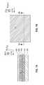
- FIG. 1Aillustrates a cross-sectional view along the line 1 A (of FIG. 1B ) and FIG. 1B illustrates a top down view of an exemplary method for forming a field effect transistor (FET) device.
- FIG. 1Aincludes a substrate 100 (for example a silicon substrate); a buried oxide (BOX) layer 102 disposed on the substrate 100 ; a silicon on insulator (SOI) layer 104 disposed on the BOX layer 102 ; a crystalline layer 106 such as, for example, a crystalline silicon germanium layer (SiGe) disposed on the SOI layer 104 ; and a second silicon layer 108 disposed on the crystalline layer 106 .
- a substrate 100for example a silicon substrate
- BOXburied oxide
- SOIsilicon on insulator
- SiGecrystalline silicon germanium layer
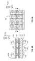
- FIGS. 2A and 2Billustrate the resultant structure including anchor portions 202 and nanowire portions 204 that are patterned in the films stack formed by layers 104 , 106 , and 108 .
- the anchor portions 202 and nanowire portions 204may be patterned by the use of lithography followed by an etching process such as, for example, reactive ion etching (RIE).
- RIEreactive ion etching
- the etching processremoves portions of the crystalline layer 108 , 106 , and the SOI layer 104 to expose portions of the BOX layer 102 .
- the rungs 204have sidewalls parallel to the ⁇ 100 ⁇ crystal planes
- the anchors 202which are connected by the rungs, have sidewalls parallel to the ⁇ 110 ⁇ crystal planes.
- the rungs and the anchorsforms a right angle)(90°, the top surface of layer 108 is therefore parallel to the ⁇ 110 ⁇ crystal planes.
- the specification for crystal planes directionsfollows the Miller indices convention which is described in, e.g., Ashcroft and Mermin, Solid State Physics, chapter 5 (1976), the contents of which are incorporated herein by reference. Following this convention a family of crystal planes, i.e.
- planes that are equivalent by the virtue of the symmetry of the crystalis typically referenced by a pair of ⁇ ⁇ parentheses.
- the planes (100), (010) and (001)are all equivalent in a cubic crystal.
- the ⁇ 110 ⁇ planesrefer collectively to the (110), (101), (011), planes.
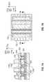
- FIGS. 3A and 3Billustrate the resultant structure following an anisotropic etching process that selectively removes portions of the crystalline layer 106 resulting in pedestal portions 302 that are defined in the crystalline layer 106 that support the anchor portions 202 .
- the anisotropic etching processremoves the portions of the crystalline layer 106 that are orientated along the lattice plane ⁇ 100 ⁇ at a faster rate than the portions of the crystalline layer 106 that are orientated along the lattice plane ⁇ 110 ⁇ , resulting in the removal of the crystalline layer 106 that is below the nanowire portions 204 , and the suspension of the nanowire portions 204 by the anchor portions 202 .
- 3Billustrates the top-down profile of the pedestal portions 302 (illustrated by the dotted lines 301 ) that support the anchor portions 202 .
- the width (w) of the pedestal portions 302is less than the width (w′) of the anchor portions 202 , resulting in longitudinal overhang regions 304 .
- the length (L) of the pedestal portions 302is less than the length (L′) of the anchor portions 202 resulting in transverse overhang regions 306 .
- the anisotropic etching processresults in the longitudinal overhang regions 304 having a smaller overhang length (W′ ⁇ W)/2 than the transverse overhang (L′ ⁇ L)/2 regions 306 due to the ⁇ 100 ⁇ planes etching faster than ⁇ 110 ⁇ planes in crystalline layer 106 .
- the anisotropic etchexhibits chemical selectivity.
- the etch chemistrymainly removes the crystalline material 106 but does not substantively etch the crystalline material 108 .
- layer 108is silicon and layer 106 is SiGe
- hot (gaseous) HCLcan be used to selectively etch SiGe with little removal of Si.
- HCLprovides an anisotropic etching process as it etches faster the SiGe in the (100) orientation than in the (110) orientation. The etching is typically done when the wafer is kept a temperature of about 800° C.
- FIGS. 4A and 4Billustrate the resultant structure following the formation of a thermal oxide layer 402 and 402 A on the exposed anchor portions 202 , nanowire portions 204 , SOI layer 104 , and pedestal portions 302 .
- the oxidation processcan be dry (with O 2 ) or wet (with H 2 O vapor), with typical oxidation temperature from 750° C. to about 1000° C.
- the thermal oxidation processcompletely oxidizes the SOI layer 104 due to the thin thickness of the SOI layer 104 relative to the thicknesses of the anchor portions 202 , nanowire portions 204 , and pedestal portions 302 .
- FIGS. 5A and 5Billustrate the resultant structure following the formation of polysilicon gates 502 and hardmask layers 504 such as, for example, silicon nitride (Si 3 N 4 ) on the polysilicon gates 502 .
- the polysilicon 502 and the hardmask layer 504may be formed by depositing polysilicon material over channel regions of the nanowire portions 204 , depositing the hardmask material over the polysilicon material, and etching by RIE to form the polysilicon gates 502 and the hardmask layers 504 .
- the etching of the polysilicon gates 502may be performed by directional etching that results in straight sidewalls of the gate 502 . Following the directional etching, polysilicon 502 remains under the nanowire portions 204 and outside the region encapsulated by the gate 502 . Isotropic etching may be performed to remove polysilicon 502 from under the nanowire portions 204 .
- FIGS. 6A and 6Billustrate spacer portions 602 formed along opposing sides of the polysilicon gates 502 .
- the spacers 602are formed by depositing a blanket dielectric film such as silicon nitride and etching the dielectric film from horizontal surfaces by RIE.
- FIGS. 6A and 6Binclude spacer portions 602 that are formed under the nanowire portions 204 , and below the overhang regions 304 and 306 .
- FIGS. 7A and 7Billustrate the resultant structures following a chemical etching process (such as etching with diluted HF) to remove the exposed portions of the thermal oxide layer 402 and a selective epitaxially grown silicon (epi-silicon) 702 that is grown on the exposed silicon of the anchor portions 202 and the nanowire portions 204 .
- the epitaxymay include, for example, the deposition of in-situ doped silicon (Si) or silicon germanium (SiGe) that may be either n-type or p-type doped.
- the in-situ doped epitaxy processforms the source region and the drain region of the nanowire FET.
- a chemical vapor deposition (CVD) reactormay be used to perform the epitaxial growth.
- Precursors for silicon epitaxyinclude SiCl 4 , SiH 4 combined with HCL. The use of chlorine allows selective deposition of silicon only on exposed silicon surfaces.
- a precursor for SiGemay include a mixture of SiCl 4 and GeH 4 .
- Precursors for dopantsmay include PH 3 or AsH 3 for n-type doping and B 2 H 6 for p-type doping.
- Deposition temperaturesmay range from 550° C. to 1000° C. for pure silicon deposition, and as low as 300° C. for pure Ge deposition.
- FIGS. 8A and 8Billustrate a resultant structure following silicidation where a silicide 802 is formed on the epi-silicon 702 of the anchor and the epi-thickened nanowire portions 202 and 204 .
- silicide forming metalsinclude Ni, Pt, Co, and alloys such as NiPt. When Ni is used the NiSi phase is typically formed due to its low resistivity. For example, formation temperatures include 400-600° C.
- capping layers and vias for connectivitymay be formed in the source (S), drain (D), and gate (G) regions of the device.
- high-K/metal gatesmay be formed on the nanowire portions 204 .
- the thermal oxide 402 around the nanowire portions 204 and along the sides of the pedestal portions 302may be removed by an etching process.
- a chemical oxide materialmay be grown on the exposed silicon material, and high-K and gate metal layers are deposited conformally prior to the deposition and etching to form the polysilicon portions 502 and hardmask layers 504 (of FIGS. 5A and 5B ).
- etchingmay be performed to remove exposed metal gate material that is not covered by the polysilicon 502 . Once the exposed metal gate material is removed, the method may continue as described in FIGS. 6A-8B above.
Landscapes
- Engineering & Computer Science (AREA)
- Chemical & Material Sciences (AREA)
- Nanotechnology (AREA)
- Physics & Mathematics (AREA)
- Crystallography & Structural Chemistry (AREA)
- Mathematical Physics (AREA)
- Theoretical Computer Science (AREA)
- Condensed Matter Physics & Semiconductors (AREA)
- General Physics & Mathematics (AREA)
- Manufacturing & Machinery (AREA)
- Thin Film Transistor (AREA)
- Electrodes Of Semiconductors (AREA)
Abstract
Description
The present invention relates to semiconductor nanowire field effect transistors and to methods that allow the fabrication of nanowire field effect transistors in a dense array.
The fabrication of a nanowire field effect transistor (FET) with a gate conductor surrounding the nanowire channel (also known as a gate-all-around nanowire FET) includes suspension of the nanowires. Suspension of the nanowires allows for the gate conductor to cover all surfaces of the nanowires.
The fabrication of a gate-all-around nanowire FET typically includes the following steps: (1) Definition of the nanowires between source and drain regions by patterning a silicon-on-insulator (SOI) layer. (2) Suspension of the nanowires by isotropic etching that undercuts the insulator on which the nanowires are resting. This etching step also undercuts the insulator at the edge of the source and drain region. The overhang/undercut that forms may not be a desirable outcome. (3) A blanket and conformal deposition of the gate conductor. The gate conductor warps around the suspended nanowires but also fills the undercut at the edge of the source and drain regions. (4) Definition of the gate line which includes the etching of the gate line and removal of gate conductor material from all regions outside the gate line, including gate material deposited in the cavities at the edge of the source and drain regions.
In one aspect of the present invention, a method for forming a nanowire field effect transistor (FET) device includes depositing a first semiconductor layer on a substrate wherein a surface of the semiconductor layer is parallel to {110} crystalline planes of the semiconductor layer, epitaxially depositing a second semiconductor layer on the first semiconductor layer, etching the first semiconductor layer and the second semiconductor layer to define a nanowire channel portion that connects a source region pad to a drain region pad, the nanowire channel portion having sidewalls that are parallel to {100} crystalline planes, and the source region pad and the drain region pad having sidewalls that are parallel to {110} crystalline planes, and performing an anisotropic etch that removes primarily material from {100} crystalline planes of the first semiconductor layer such that the nanowire channel portion is suspended by the source region pad and the drain region pad.
In another aspect of the present invention, a method for forming a nanowire field effect transistor (FET) device includes disposing a crystalline layer on a substrate, disposing a silicon layer on the crystalline layer, etching the portions of the silicon layer and the crystalline layer to define a nanowire portion in the silicon layer having a longitudinal orientation along a lattice plane (110) of the crystalline layer, the nanowire portion connected to a first anchor portion having a longitudinal orientation along a lattice plane (001) of the crystalline layer and a second anchor portion having a longitudinal orientation along the lattice plane (001) of the crystalline layer, anisotropically etching to primarily remove the crystalline layer under the nanowire portion and marginally etching a portion of the crystalline layer under the first anchor portion and a portion of the crystalline layer under the second anchor portion, and forming a gate structure on a channel region of the nanowire.
In yet another aspect of the present invention, a nanowire field effect transistor (FET) device includes a source region comprising a first semiconductor layer disposed on a second semiconductor layer, the source region having a surface parallel to {110} crystalline planes and opposing sidewall surfaces parallel to the {110} crystalline planes, a drain region comprising the first semiconductor layer disposed on the second semiconductor layer, the source region having a face parallel to the {110} crystalline planes and opposing sidewall surfaces parallel to the {110} crystalline planes, a nanowire channel member suspended by the source region and the drain region, wherein nanowire channel includes the first semiconductor layer, and opposing sidewall surfaces parallel to {100} crystalline planes and opposing faces parallel to the {110} crystalline planes.
Additional features and advantages are realized through the techniques of the present invention. Other embodiments and aspects of the invention are described in detail herein and are considered a part of the claimed invention. For a better understanding of the invention with the advantages and the features, refer to the description and to the drawings.
The subject matter which is regarded as the invention is particularly pointed out and distinctly claimed in the claims at the conclusion of the specification. The forgoing and other features, and advantages of the invention are apparent from the following detailed description taken in conjunction with the accompanying drawings in which:
The formation of the undercut (in step 3; described in the Description of Related Art section above) imposes a limitation on the density of circuits built with gate-all-around nanowire FET. The undercut size should be at least half of the width of the nanowires, or the nanowires may not be fully suspended by the etching. The undercut under the source (or drain) region should be smaller than half of the source (or drain) region width. If the source width is made narrower than two times the undercut size, the source (and drain) may not provide the anchoring for the suspended nanowires. The minimum width of the source and the drain dictates the area the device occupies. In addition to the circuit density limitation the presence of the undercut may lead to fabrication issues. The definition of the gate line (step 4) includes the removal of all the gate conductor material that was deposited in the cavity formed by the undercut. This is typically performed by an isotropic etch, which also etches the gate line. As a result, control of the gate line dimensions may be difficult to obtain.
In an alternate exemplary method, high-K/metal gates may be formed on thenanowire portions 204. Referring toFIGS. 4A and 4B , thethermal oxide 402 around thenanowire portions 204 and along the sides of thepedestal portions 302 may be removed by an etching process. A chemical oxide material may be grown on the exposed silicon material, and high-K and gate metal layers are deposited conformally prior to the deposition and etching to form thepolysilicon portions 502 and hardmask layers504 (ofFIGS. 5A and 5B ). Once thepolysilicon 502 andhardmask layers 504 are formed, etching may be performed to remove exposed metal gate material that is not covered by thepolysilicon 502. Once the exposed metal gate material is removed, the method may continue as described inFIGS. 6A-8B above.
The terminology used herein is for the purpose of describing particular embodiments only and is not intended to be limiting of the invention. As used herein, the singular forms “a”, “an” and “the” are intended to include the plural forms as well, unless the context clearly indicates otherwise. It will be further understood that the terms “comprises” and/or “comprising,” when used in this specification, specify the presence of stated features, integers, steps, operations, elements, and/or components, but do not preclude the presence or addition of one or more other features, integers, steps, operations, element components, and/or groups thereof.
The corresponding structures, materials, acts, and equivalents of all means or step plus function elements in the claims below are intended to include any structure, material, or act for performing the function in combination with other claimed elements as specifically claimed. The description of the present invention has been presented for purposes of illustration and description, but is not intended to be exhaustive or limited to the invention in the form disclosed. Many modifications and variations will be apparent to those of ordinary skill in the art without departing from the scope and spirit of the invention. The embodiment was chosen and described in order to best explain the principles of the invention and the practical application, and to enable others of ordinary skill in the art to understand the invention for various embodiments with various modifications as are suited to the particular use contemplated
The diagrams depicted herein are just one example. There may be many variations to this diagram or the steps (or operations) described therein without departing from the spirit of the invention. For instance, the steps may be performed in a differing order or steps may be added, deleted or modified. All of these variations are considered a part of the claimed invention.
While the preferred embodiment to the invention had been described, it will be understood that those skilled in the art, both now and in the future, may make various improvements and enhancements which fall within the scope of the claims which follow. These claims should be construed to maintain the proper protection for the invention first described.
Claims (15)
1. A method comprising:
depositing a first semiconductor layer on a substrate wherein a surface of the first semiconductor layer is parallel to {110} crystalline planes of the first semiconductor layer;
epitaxially depositing a second semiconductor layer on the first semiconductor layer;
etching the first semiconductor layer and the second semiconductor layer to define a nanowire portion that connects a first anchor portion to a second anchor portion, the nanowire portion having sidewalls that are parallel to {100} crystalline planes, the first anchor portion and the second anchor portion having sidewalls that are parallel to {110} crystalline planes; and
performing an anisotropic etch that removes primarily material from {100} crystalline planes of the first semiconductor layer such that the nanowire portion is suspended by the first anchor portion and the second anchor portion.
2. The method ofclaim 1 , wherein first semiconductor layer includes SiGe, and the second semiconductor layer includes silicon.
3. The method ofclaim 1 , wherein substrate is a silicon-on-insulator (SOI) wafer comprising:
a handle wafer;
an insulator formed on the handle wafer; and
a silicon-on-insulator formed on the insulator layer.
4. The method ofclaim 1 further comprising forming a gate-all-around the suspended nanowire portion.
5. The method ofclaim 3 , further comprising oxidizing the silicon-on-insulator layer to form an insulator.
6. The method ofclaim 1 , wherein performing an anisotropic etch include etching with hot gaseous HCL.
7. The method ofclaim 1 , wherein anisotropic etch is chemically selective to primarily remove portions of the first semiconductor layer.
8. A method comprising:
disposing a crystalline layer on a substrate;
disposing a silicon layer on the crystalline layer;
etching the portions of the silicon layer and the crystalline layer to define a nanowire portion in the silicon layer having a longitudinal orientation along a lattice plane (110) of the crystalline layer, the nanowire portion connected to a first anchor portion having a longitudinal orientation along a lattice plane (001) of the crystalline layer and a second anchor portion having a longitudinal orientation along the lattice plane (001) of the crystalline layer;
anisotropically etching to primarily remove the crystalline layer under the nanowire portion and marginally etching a portion of the crystalline layer under the first anchor portion and a portion of the crystalline layer under the second anchor portion; and
forming a gate structure on a channel region of the nanowire.
9. The method ofclaim 8 , wherein the etching to remove the crystalline layer under the nanowire portion includes an anisotropic etching process that is operative to remove exposed portions of the crystalline layer having sidewalls parallel to lattice plane (100) at a faster rate than exposed portions of the crystalline layer having sidewalls parallel to lattice plane (110).
10. The method ofclaim 8 , wherein the substrate includes a silicon on insulator (SOI) layer disposed on a buried oxide (BOX) layer, and the crystalline layer is disposed on the SOI layer.
11. The method ofclaim 10 , wherein etching the portions of the silicon layer and the crystalline layer to define a nanowire portion in the silicon layer includes etching portions of the SOI layer.
12. The method ofclaim 10 , wherein the method further includes oxidizing exposed portions of the nanowire portion, and the SOI layer prior to forming the gate structure.
13. The method ofclaim 12 , wherein the method further includes removing the exposed oxidized portions of the nanowire portion and the SOI layer.
14. The method ofclaim 8 , wherein the method further includes epitaxially growing a silicon material on the nanowire portion.
15. The method ofclaim 8 , wherein an amount of anisotropically etching to primarily remove the crystalline layer under the nanowire portion and marginally etching a portion of the crystalline layer under the first anchor portion is controlled by crystalline orientation.
Priority Applications (4)
| Application Number | Priority Date | Filing Date | Title |
|---|---|---|---|
| US12/776,485US8361907B2 (en) | 2010-05-10 | 2010-05-10 | Directionally etched nanowire field effect transistors |
| PCT/EP2011/053174WO2011141193A1 (en) | 2010-05-10 | 2011-03-03 | Directionally etched nanowire field effect transistors |
| TW100116200ATW201203390A (en) | 2010-05-10 | 2011-05-09 | Directionally etched nanowire field effect transistors |
| US13/550,700US8772755B2 (en) | 2010-05-10 | 2012-07-17 | Directionally etched nanowire field effect transistors |
Applications Claiming Priority (1)
| Application Number | Priority Date | Filing Date | Title |
|---|---|---|---|
| US12/776,485US8361907B2 (en) | 2010-05-10 | 2010-05-10 | Directionally etched nanowire field effect transistors |
Related Child Applications (1)
| Application Number | Title | Priority Date | Filing Date |
|---|---|---|---|
| US13/550,700DivisionUS8772755B2 (en) | 2010-05-10 | 2012-07-17 | Directionally etched nanowire field effect transistors |
Publications (2)
| Publication Number | Publication Date |
|---|---|
| US20110272673A1 US20110272673A1 (en) | 2011-11-10 |
| US8361907B2true US8361907B2 (en) | 2013-01-29 |
Family
ID=43983633
Family Applications (2)
| Application Number | Title | Priority Date | Filing Date |
|---|---|---|---|
| US12/776,485Expired - Fee RelatedUS8361907B2 (en) | 2010-05-10 | 2010-05-10 | Directionally etched nanowire field effect transistors |
| US13/550,700ActiveUS8772755B2 (en) | 2010-05-10 | 2012-07-17 | Directionally etched nanowire field effect transistors |
Family Applications After (1)
| Application Number | Title | Priority Date | Filing Date |
|---|---|---|---|
| US13/550,700ActiveUS8772755B2 (en) | 2010-05-10 | 2012-07-17 | Directionally etched nanowire field effect transistors |
Country Status (3)
| Country | Link |
|---|---|
| US (2) | US8361907B2 (en) |
| TW (1) | TW201203390A (en) |
| WO (1) | WO2011141193A1 (en) |
Cited By (1)
| Publication number | Priority date | Publication date | Assignee | Title |
|---|---|---|---|---|
| US9362354B1 (en) | 2015-02-18 | 2016-06-07 | International Business Machines Corporation | Tuning gate lengths in semiconductor device structures |
Families Citing this family (9)
| Publication number | Priority date | Publication date | Assignee | Title |
|---|---|---|---|---|
| US10483385B2 (en)* | 2011-12-23 | 2019-11-19 | Intel Corporation | Nanowire structures having wrap-around contacts |
| US8987835B2 (en)* | 2012-03-27 | 2015-03-24 | Taiwan Semiconductor Manufacturing Company, Ltd. | FinFET with a buried semiconductor material between two fins |
| US9006810B2 (en)* | 2012-06-07 | 2015-04-14 | International Business Machines Corporation | DRAM with a nanowire access transistor |
| US8735869B2 (en)* | 2012-09-27 | 2014-05-27 | Intel Corporation | Strained gate-all-around semiconductor devices formed on globally or locally isolated substrates |
| US9000530B2 (en) | 2013-04-23 | 2015-04-07 | International Business Machines Corporation | 6T SRAM architecture for gate-all-around nanowire devices |
| WO2016105408A1 (en)* | 2014-12-24 | 2016-06-30 | Intel Corporation | Field effect transistor structures using germanium nanowires |
| US9647139B2 (en) | 2015-09-04 | 2017-05-09 | International Business Machines Corporation | Atomic layer deposition sealing integration for nanosheet complementary metal oxide semiconductor with replacement spacer |
| US10332986B2 (en) | 2016-08-22 | 2019-06-25 | International Business Machines Corporation | Formation of inner spacer on nanosheet MOSFET |
| FR3081154B1 (en)* | 2018-05-17 | 2023-08-04 | Commissariat Energie Atomique | METHOD FOR MANUFACTURING AN ELECTRONIC COMPONENT WITH MULTIPLE QUANTUM ISLANDS |
Citations (75)
| Publication number | Priority date | Publication date | Assignee | Title |
|---|---|---|---|---|
| EP0217811A1 (en) | 1985-03-18 | 1987-04-15 | Caterpillar Inc | Engine having a multipiece cylinder block. |
| US4995001A (en) | 1988-10-31 | 1991-02-19 | International Business Machines Corporation | Memory cell and read circuit |
| US5308445A (en) | 1991-10-23 | 1994-05-03 | Rohm Co., Ltd. | Method of manufacturing a semiconductor device having a semiconductor growth layer completely insulated from a substrate |
| US5438018A (en) | 1992-12-07 | 1995-08-01 | Fujitsu Limited | Method of making semiconductor device by selective epitaxial growth |
| US5552622A (en) | 1992-07-14 | 1996-09-03 | Mitsuteru Kimura | Tunnel transistor |
| US5668046A (en) | 1991-03-27 | 1997-09-16 | Nec Corporation | Method of producing a semiconductor on insulating substrate, and a method of forming transistor thereon |
| US6365465B1 (en) | 1999-03-19 | 2002-04-02 | International Business Machines Corporation | Self-aligned double-gate MOSFET by selective epitaxy and silicon wafer bonding techniques |
| WO2002084757A1 (en) | 2001-04-12 | 2002-10-24 | Infineon Technologies Ag | Heterostructure component |
| US6642115B1 (en) | 2000-05-15 | 2003-11-04 | International Business Machines Corporation | Double-gate FET with planarized surfaces and self-aligned silicides |
| US6653209B1 (en) | 1999-09-30 | 2003-11-25 | Canon Kabushiki Kaisha | Method of producing silicon thin film, method of constructing SOI substrate and semiconductor device |
| US20040149978A1 (en) | 2003-01-31 | 2004-08-05 | Greg Snider | Molecular-junction-nanowire-crossbar-based inverter, latch, and flip-flop circuits, and more complex circuits composed, in part, from molecular-junction-nanowire-crossbar-based inverter, latch, and flip-flop circuits |
| US20040166642A1 (en) | 2003-02-20 | 2004-08-26 | Hao-Yu Chen | Semiconductor nano-rod devices |
| US6806141B2 (en) | 2002-05-22 | 2004-10-19 | Hewlett-Packard Development Company, L.P. | Field effect transistor with gate layer and method of making same |
| US6882051B2 (en) | 2001-03-30 | 2005-04-19 | The Regents Of The University Of California | Nanowires, nanostructures and devices fabricated therefrom |
| US6891227B2 (en) | 2002-03-20 | 2005-05-10 | International Business Machines Corporation | Self-aligned nanotube field effect transistor and method of fabricating same |
| US6903013B2 (en) | 2003-05-16 | 2005-06-07 | Chartered Semiconductor Manufacturing Ltd. | Method to fill a trench and tunnel by using ALD seed layer and electroless plating |
| US20050266645A1 (en) | 2004-05-25 | 2005-12-01 | Jin-Jun Park | Phosphorous doping methods of manufacturing field effect transistors having multiple stacked channels |
| US20050275010A1 (en) | 2004-06-10 | 2005-12-15 | Hung-Wei Chen | Semiconductor nano-wire devices and methods of fabrication |
| US20060033145A1 (en) | 2004-08-13 | 2006-02-16 | Ronald Kakoschke | Integrated memory device and process |
| US7101762B2 (en) | 2000-07-07 | 2006-09-05 | International Business Machines Corporation | Self-aligned double gate mosfet with separate gates |
| US7151209B2 (en) | 2002-04-02 | 2006-12-19 | Nanosys, Inc. | Methods of making, positioning and orienting nanostructures, nanostructure arrays and nanostructure devices |
| US20070001219A1 (en) | 2005-06-30 | 2007-01-04 | Marko Radosavljevic | Block contact architectures for nanoscale channel transistors |
| US7180107B2 (en) | 2004-05-25 | 2007-02-20 | International Business Machines Corporation | Method of fabricating a tunneling nanotube field effect transistor |
| US7253060B2 (en) | 2004-06-08 | 2007-08-07 | Samsung Electronics Co., Ltd. | Gate-all-around type of semiconductor device and method of fabricating the same |
| US7297615B2 (en) | 2005-05-13 | 2007-11-20 | Samsung Electronics, Co., Ltd. | Si nanowire substrate, method of manufacturing the same, and method of manufacturing thin film transistor using the same |
| US20070267703A1 (en) | 2006-05-17 | 2007-11-22 | Chartered Semiconductor Manufacturing Ltd. | Strained channel transistor and method of fabrication thereof |
| US20070267619A1 (en) | 2006-05-22 | 2007-11-22 | Thomas Nirschl | Memory using tunneling field effect transistors |
| US20070284613A1 (en) | 2006-06-09 | 2007-12-13 | Chi On Chui | Strain-inducing semiconductor regions |
| US7311776B2 (en) | 2003-12-30 | 2007-12-25 | The Regents Of The University Of California | Localized synthesis and self-assembly of nanostructures |
| US20080014689A1 (en) | 2006-07-07 | 2008-01-17 | Texas Instruments Incorporated | Method for making planar nanowire surround gate mosfet |
| US20080061284A1 (en) | 2006-09-11 | 2008-03-13 | International Business Machines Corporation | Nanowire MOSFET with doped epitaxial contacts for source and drain |
| US20080067607A1 (en) | 2006-09-15 | 2008-03-20 | Interuniversitair Microelektronica Centrum (Imec) | Tunnel effect transistors based on elongate monocrystalline nanostructures having a heterostructure |
| US20080067495A1 (en) | 2006-09-15 | 2008-03-20 | Interuniversitair Microelektronica Centrum (Imec) | Tunnel effect transistors based on silicon nanowires |
| US20080079041A1 (en) | 2006-10-02 | 2008-04-03 | Samsung Electronics Co, Ltd. | Gate-all-around type semiconductor device and method of manufacturing the same |
| US20080085587A1 (en) | 2006-10-04 | 2008-04-10 | Micron Technology, Inc. | Epitaxial silicon growth |
| US20080121932A1 (en) | 2006-09-18 | 2008-05-29 | Pushkar Ranade | Active regions with compatible dielectric layers |
| US20080128760A1 (en)* | 2006-12-04 | 2008-06-05 | Electronics And Telecommunications Research Institute | Schottky barrier nanowire field effect transistor and method for fabricating the same |
| WO2008069765A1 (en) | 2006-12-08 | 2008-06-12 | Agency For Science, Technology And Research | A stacked silicon-germanium nanowire structure and a method of forming the same |
| US20080142853A1 (en) | 2005-08-08 | 2008-06-19 | Freescale Semiconductor, Inc. | Multi-channel transistor structure and method of making thereof |
| US20080149914A1 (en) | 2006-12-22 | 2008-06-26 | Qunano Ab | Nanoelectronic structure and method of producing such |
| US20080149997A1 (en) | 2006-12-20 | 2008-06-26 | Samsung Electronics Co., Ltd. | Nonvolatile memory device and method of operating the same |
| US20080150025A1 (en) | 2005-12-13 | 2008-06-26 | Versatilis Llc | Methods of Making Semiconductor-Based Electronic Devices on a Wire and by Forming Freestanding Semiconductor Structures, and Devices That Can Be Made Thereby |
| US20080179752A1 (en) | 2007-01-26 | 2008-07-31 | Takashi Yamauchi | Method of making semiconductor device and semiconductor device |
| US20080191196A1 (en) | 2005-06-06 | 2008-08-14 | Wei Lu | Nanowire heterostructures |
| US20080227259A1 (en) | 2005-01-07 | 2008-09-18 | International Business Machines Corporation | SELF-ALIGNED PROCESS FOR NANOTUBE/NANOWIRE FETs |
| US20080224224A1 (en) | 2007-03-12 | 2008-09-18 | Interuniversitair Microelektronica Centrum Vzw (Imec) | Tunnel field-effect transistor with gated tunnel barrier |
| US20080247226A1 (en) | 2007-04-05 | 2008-10-09 | Micron Technology, Inc. | Memory devices having electrodes comprising nanowires, systems including same and methods of forming same |
| US20080246021A1 (en) | 2006-10-04 | 2008-10-09 | Samsung Electronic Co., Ltd., | Single electron transistor and method of manufacturing the same |
| US7443025B2 (en) | 2004-06-07 | 2008-10-28 | Broadcom Corporation | Thermally improved placement of power-dissipating components onto a circuit board |
| US7446025B2 (en) | 2005-05-23 | 2008-11-04 | International Business Machines Corporation | Method of forming vertical FET with nanowire channels and a silicided bottom contact |
| US7449373B2 (en) | 2006-03-31 | 2008-11-11 | Intel Corporation | Method of ion implanting for tri-gate devices |
| US7452759B2 (en) | 2005-11-29 | 2008-11-18 | Micron Technology, Inc. | Carbon nanotube field effect transistor and methods for making same |
| US7456476B2 (en) | 2003-06-27 | 2008-11-25 | Intel Corporation | Nonplanar semiconductor device with partially or fully wrapped around gate electrode and methods of fabrication |
| US7456068B2 (en) | 2006-06-08 | 2008-11-25 | Intel Corporation | Forming ultra-shallow junctions |
| US20080290418A1 (en) | 2007-05-25 | 2008-11-27 | Kalburge Amol M | Method for Integrating Nanotube Devices with CMOS for RF/Analog SoC Applications |
| US7473943B2 (en) | 2004-10-15 | 2009-01-06 | Nanosys, Inc. | Gate configuration for nanowire electronic devices |
| US20090026553A1 (en) | 2007-07-25 | 2009-01-29 | Krishna Kumar Bhuwalka | Tunnel Field-Effect Transistor with Narrow Band-Gap Channel and Strong Gate Coupling |
| US7498211B2 (en) | 2005-12-28 | 2009-03-03 | Intel Corporation | Independently controlled, double gate nanowire memory cell with self-aligned contacts |
| US20090061568A1 (en) | 2007-09-05 | 2009-03-05 | International Business Machines Corporation | Techniques for Fabricating Nanowire Field-Effect Transistors |
| US20090057762A1 (en) | 2007-09-05 | 2009-03-05 | International Business Machines Corporation | Nanowire Field-Effect Transistors |
| US20090057650A1 (en) | 2000-08-22 | 2009-03-05 | President And Fellows Of Harvard College | Nanoscale wires and related devices |
| US20090090934A1 (en) | 2007-10-05 | 2009-04-09 | Tsutomu Tezuka | Field Effect Transistor and Method for Manufacturing the Same |
| KR20090044799A (en) | 2007-11-01 | 2009-05-07 | 삼성전자주식회사 | Method for manufacturing active fin and transistor comprising same |
| US20090134467A1 (en) | 2007-11-26 | 2009-05-28 | Renesas Technology Corp. | Semiconductor device and a method of manufacturing the same |
| US20090149012A1 (en) | 2004-09-30 | 2009-06-11 | Brask Justin K | Method of forming a nonplanar transistor with sidewall spacers |
| US7550333B2 (en) | 2004-10-25 | 2009-06-23 | Intel Corporation | Nonplanar device with thinned lower body portion and method of fabrication |
| US20090181477A1 (en) | 2005-07-01 | 2009-07-16 | Synopsys, Inc. | Integrated Circuit On Corrugated Substrate |
| US20090294864A1 (en) | 2005-06-13 | 2009-12-03 | Samsung Electronics Co., Ltd. | Mos field effect transistor having plurality of channels |
| US7642578B2 (en) | 2005-03-24 | 2010-01-05 | Samsung Electronics Co., Ltd. | Semiconductor device having a round-shaped nano-wire transistor channel and method of manufacturing same |
| US20100193770A1 (en) | 2009-02-04 | 2010-08-05 | International Business Machines Corporation | Maskless Process for Suspending and Thinning Nanowires |
| US7791144B2 (en) | 2006-04-28 | 2010-09-07 | International Business Machines Corporation | High performance stress-enhance MOSFET and method of manufacture |
| US7799657B2 (en) | 2005-06-07 | 2010-09-21 | Freescale Semiconductor, Inc. | Method of fabricating a substrate for a planar, double-gated, transistor process |
| US7834345B2 (en) | 2008-09-05 | 2010-11-16 | Taiwan Semiconductor Manufacturing Company, Ltd. | Tunnel field-effect transistors with superlattice channels |
| US7893506B2 (en) | 2005-02-23 | 2011-02-22 | Intel Corporation | Field effect transistor with narrow bandgap source and drain regions and method of fabrication |
| US20110133169A1 (en) | 2009-12-04 | 2011-06-09 | International Business Machines Corporation | Gate-All-Around Nanowire Tunnel Field Effect Transistors |
Family Cites Families (18)
| Publication number | Priority date | Publication date | Assignee | Title |
|---|---|---|---|---|
| WO2003010837A1 (en) | 2001-07-26 | 2003-02-06 | Technische Universiteit Delft | Electronic device using carbon nanotubes |
| US6835618B1 (en) | 2003-08-05 | 2004-12-28 | Advanced Micro Devices, Inc. | Epitaxially grown fin for FinFET |
| US7060576B2 (en) | 2003-10-24 | 2006-06-13 | Intel Corporation | Epitaxially deposited source/drain |
| US7402872B2 (en) | 2004-11-18 | 2008-07-22 | Intel Corporation | Method for forming an integrated circuit |
| KR100745769B1 (en) | 2006-09-11 | 2007-08-02 | 삼성전자주식회사 | Nanowire electromechanical switching device and manufacturing method thereof, electromechanical memory device using the nanowire electromechanical device |
| US20090217216A1 (en) | 2007-02-28 | 2009-08-27 | Motorola, Inc. | Carbon nanotube circuits design methodology |
| US8154127B1 (en) | 2007-07-30 | 2012-04-10 | Hewlett-Packard Development Company, L.P. | Optical device and method of making the same |
| FR2937463B1 (en)* | 2008-10-17 | 2010-12-24 | Commissariat Energie Atomique | METHOD FOR MANUFACTURING STACKED AND SELF-ALIGNED COMPONENTS ON A SUBSTRATE |
| US8362604B2 (en) | 2008-12-04 | 2013-01-29 | Ecole Polytechnique Federale De Lausanne (Epfl) | Ferroelectric tunnel FET switch and memory |
| KR20100094192A (en) | 2009-02-18 | 2010-08-26 | 삼성전자주식회사 | Static random access memory using carbon nanotube thin films |
| US8368125B2 (en)* | 2009-07-20 | 2013-02-05 | International Business Machines Corporation | Multiple orientation nanowires with gate stack stressors |
| US8097515B2 (en) | 2009-12-04 | 2012-01-17 | International Business Machines Corporation | Self-aligned contacts for nanowire field effect transistors |
| US8129247B2 (en) | 2009-12-04 | 2012-03-06 | International Business Machines Corporation | Omega shaped nanowire field effect transistors |
| US8455334B2 (en)* | 2009-12-04 | 2013-06-04 | International Business Machines Corporation | Planar and nanowire field effect transistors |
| US20110147840A1 (en) | 2009-12-23 | 2011-06-23 | Cea Stephen M | Wrap-around contacts for finfet and tri-gate devices |
| US8420455B2 (en) | 2010-05-12 | 2013-04-16 | International Business Machines Corporation | Generation of multiple diameter nanowire field effect transistors |
| US8338280B2 (en) | 2010-07-08 | 2012-12-25 | Globalfoundries Singapore Pte. Ltd. | Method for fabricating nano devices |
| US8716072B2 (en)* | 2011-07-25 | 2014-05-06 | International Business Machines Corporation | Hybrid CMOS technology with nanowire devices and double gated planar devices |
- 2010
- 2010-05-10USUS12/776,485patent/US8361907B2/ennot_activeExpired - Fee Related
- 2011
- 2011-03-03WOPCT/EP2011/053174patent/WO2011141193A1/enactiveApplication Filing
- 2011-05-09TWTW100116200Apatent/TW201203390A/enunknown
- 2012
- 2012-07-17USUS13/550,700patent/US8772755B2/enactiveActive
Patent Citations (84)
| Publication number | Priority date | Publication date | Assignee | Title |
|---|---|---|---|---|
| EP0217811A1 (en) | 1985-03-18 | 1987-04-15 | Caterpillar Inc | Engine having a multipiece cylinder block. |
| US4995001A (en) | 1988-10-31 | 1991-02-19 | International Business Machines Corporation | Memory cell and read circuit |
| US5668046A (en) | 1991-03-27 | 1997-09-16 | Nec Corporation | Method of producing a semiconductor on insulating substrate, and a method of forming transistor thereon |
| US5308445A (en) | 1991-10-23 | 1994-05-03 | Rohm Co., Ltd. | Method of manufacturing a semiconductor device having a semiconductor growth layer completely insulated from a substrate |
| US5552622A (en) | 1992-07-14 | 1996-09-03 | Mitsuteru Kimura | Tunnel transistor |
| US5438018A (en) | 1992-12-07 | 1995-08-01 | Fujitsu Limited | Method of making semiconductor device by selective epitaxial growth |
| US5574308A (en) | 1992-12-07 | 1996-11-12 | Fujitsu Limited | Semiconductor device and its manufacturing method |
| US6365465B1 (en) | 1999-03-19 | 2002-04-02 | International Business Machines Corporation | Self-aligned double-gate MOSFET by selective epitaxy and silicon wafer bonding techniques |
| US6653209B1 (en) | 1999-09-30 | 2003-11-25 | Canon Kabushiki Kaisha | Method of producing silicon thin film, method of constructing SOI substrate and semiconductor device |
| US6642115B1 (en) | 2000-05-15 | 2003-11-04 | International Business Machines Corporation | Double-gate FET with planarized surfaces and self-aligned silicides |
| US7101762B2 (en) | 2000-07-07 | 2006-09-05 | International Business Machines Corporation | Self-aligned double gate mosfet with separate gates |
| US20090057650A1 (en) | 2000-08-22 | 2009-03-05 | President And Fellows Of Harvard College | Nanoscale wires and related devices |
| US7569941B2 (en) | 2001-03-30 | 2009-08-04 | The Regents Of The University Of California | Methods of fabricating nanostructures and nanowires and devices fabricated therefrom |
| US6882051B2 (en) | 2001-03-30 | 2005-04-19 | The Regents Of The University Of California | Nanowires, nanostructures and devices fabricated therefrom |
| US6996147B2 (en) | 2001-03-30 | 2006-02-07 | The Regents Of The University Of California | Methods of fabricating nanostructures and nanowires and devices fabricated therefrom |
| WO2002084757A1 (en) | 2001-04-12 | 2002-10-24 | Infineon Technologies Ag | Heterostructure component |
| US6891227B2 (en) | 2002-03-20 | 2005-05-10 | International Business Machines Corporation | Self-aligned nanotube field effect transistor and method of fabricating same |
| US7151209B2 (en) | 2002-04-02 | 2006-12-19 | Nanosys, Inc. | Methods of making, positioning and orienting nanostructures, nanostructure arrays and nanostructure devices |
| US6806141B2 (en) | 2002-05-22 | 2004-10-19 | Hewlett-Packard Development Company, L.P. | Field effect transistor with gate layer and method of making same |
| US20040149978A1 (en) | 2003-01-31 | 2004-08-05 | Greg Snider | Molecular-junction-nanowire-crossbar-based inverter, latch, and flip-flop circuits, and more complex circuits composed, in part, from molecular-junction-nanowire-crossbar-based inverter, latch, and flip-flop circuits |
| US20050121706A1 (en) | 2003-02-20 | 2005-06-09 | Hao-Yu Chen | Semiconductor nano-rod devices |
| US20040166642A1 (en) | 2003-02-20 | 2004-08-26 | Hao-Yu Chen | Semiconductor nano-rod devices |
| US6855606B2 (en) | 2003-02-20 | 2005-02-15 | Taiwan Semiconductor Manufacturing Company, Ltd. | Semiconductor nano-rod devices |
| US6903013B2 (en) | 2003-05-16 | 2005-06-07 | Chartered Semiconductor Manufacturing Ltd. | Method to fill a trench and tunnel by using ALD seed layer and electroless plating |
| US7456476B2 (en) | 2003-06-27 | 2008-11-25 | Intel Corporation | Nonplanar semiconductor device with partially or fully wrapped around gate electrode and methods of fabrication |
| US7311776B2 (en) | 2003-12-30 | 2007-12-25 | The Regents Of The University Of California | Localized synthesis and self-assembly of nanostructures |
| US20050266645A1 (en) | 2004-05-25 | 2005-12-01 | Jin-Jun Park | Phosphorous doping methods of manufacturing field effect transistors having multiple stacked channels |
| US7180107B2 (en) | 2004-05-25 | 2007-02-20 | International Business Machines Corporation | Method of fabricating a tunneling nanotube field effect transistor |
| US7443025B2 (en) | 2004-06-07 | 2008-10-28 | Broadcom Corporation | Thermally improved placement of power-dissipating components onto a circuit board |
| US7253060B2 (en) | 2004-06-08 | 2007-08-07 | Samsung Electronics Co., Ltd. | Gate-all-around type of semiconductor device and method of fabricating the same |
| US20050275010A1 (en) | 2004-06-10 | 2005-12-15 | Hung-Wei Chen | Semiconductor nano-wire devices and methods of fabrication |
| US7452778B2 (en) | 2004-06-10 | 2008-11-18 | Taiwan Semiconductor Manufacturing Company, Ltd. | Semiconductor nano-wire devices and methods of fabrication |
| US20060033145A1 (en) | 2004-08-13 | 2006-02-16 | Ronald Kakoschke | Integrated memory device and process |
| US20090149012A1 (en) | 2004-09-30 | 2009-06-11 | Brask Justin K | Method of forming a nonplanar transistor with sidewall spacers |
| US7473943B2 (en) | 2004-10-15 | 2009-01-06 | Nanosys, Inc. | Gate configuration for nanowire electronic devices |
| US7871870B2 (en) | 2004-10-15 | 2011-01-18 | Nanosys, Inc. | Method of fabricating gate configurations for an improved contacts in nanowire based electronic devices |
| US7550333B2 (en) | 2004-10-25 | 2009-06-23 | Intel Corporation | Nonplanar device with thinned lower body portion and method of fabrication |
| US20080227259A1 (en) | 2005-01-07 | 2008-09-18 | International Business Machines Corporation | SELF-ALIGNED PROCESS FOR NANOTUBE/NANOWIRE FETs |
| US7893506B2 (en) | 2005-02-23 | 2011-02-22 | Intel Corporation | Field effect transistor with narrow bandgap source and drain regions and method of fabrication |
| US7642578B2 (en) | 2005-03-24 | 2010-01-05 | Samsung Electronics Co., Ltd. | Semiconductor device having a round-shaped nano-wire transistor channel and method of manufacturing same |
| US7297615B2 (en) | 2005-05-13 | 2007-11-20 | Samsung Electronics, Co., Ltd. | Si nanowire substrate, method of manufacturing the same, and method of manufacturing thin film transistor using the same |
| US7446025B2 (en) | 2005-05-23 | 2008-11-04 | International Business Machines Corporation | Method of forming vertical FET with nanowire channels and a silicided bottom contact |
| US20080191196A1 (en) | 2005-06-06 | 2008-08-14 | Wei Lu | Nanowire heterostructures |
| US7799657B2 (en) | 2005-06-07 | 2010-09-21 | Freescale Semiconductor, Inc. | Method of fabricating a substrate for a planar, double-gated, transistor process |
| US20090294864A1 (en) | 2005-06-13 | 2009-12-03 | Samsung Electronics Co., Ltd. | Mos field effect transistor having plurality of channels |
| US20070001219A1 (en) | 2005-06-30 | 2007-01-04 | Marko Radosavljevic | Block contact architectures for nanoscale channel transistors |
| US20090181477A1 (en) | 2005-07-01 | 2009-07-16 | Synopsys, Inc. | Integrated Circuit On Corrugated Substrate |
| US20080142853A1 (en) | 2005-08-08 | 2008-06-19 | Freescale Semiconductor, Inc. | Multi-channel transistor structure and method of making thereof |
| US7452759B2 (en) | 2005-11-29 | 2008-11-18 | Micron Technology, Inc. | Carbon nanotube field effect transistor and methods for making same |
| US20080150025A1 (en) | 2005-12-13 | 2008-06-26 | Versatilis Llc | Methods of Making Semiconductor-Based Electronic Devices on a Wire and by Forming Freestanding Semiconductor Structures, and Devices That Can Be Made Thereby |
| US7498211B2 (en) | 2005-12-28 | 2009-03-03 | Intel Corporation | Independently controlled, double gate nanowire memory cell with self-aligned contacts |
| US7449373B2 (en) | 2006-03-31 | 2008-11-11 | Intel Corporation | Method of ion implanting for tri-gate devices |
| US7791144B2 (en) | 2006-04-28 | 2010-09-07 | International Business Machines Corporation | High performance stress-enhance MOSFET and method of manufacture |
| US20070267703A1 (en) | 2006-05-17 | 2007-11-22 | Chartered Semiconductor Manufacturing Ltd. | Strained channel transistor and method of fabrication thereof |
| US20070267619A1 (en) | 2006-05-22 | 2007-11-22 | Thomas Nirschl | Memory using tunneling field effect transistors |
| US7456068B2 (en) | 2006-06-08 | 2008-11-25 | Intel Corporation | Forming ultra-shallow junctions |
| US20070284613A1 (en) | 2006-06-09 | 2007-12-13 | Chi On Chui | Strain-inducing semiconductor regions |
| US20080014689A1 (en) | 2006-07-07 | 2008-01-17 | Texas Instruments Incorporated | Method for making planar nanowire surround gate mosfet |
| US20080061284A1 (en) | 2006-09-11 | 2008-03-13 | International Business Machines Corporation | Nanowire MOSFET with doped epitaxial contacts for source and drain |
| US20080067607A1 (en) | 2006-09-15 | 2008-03-20 | Interuniversitair Microelektronica Centrum (Imec) | Tunnel effect transistors based on elongate monocrystalline nanostructures having a heterostructure |
| US20080067495A1 (en) | 2006-09-15 | 2008-03-20 | Interuniversitair Microelektronica Centrum (Imec) | Tunnel effect transistors based on silicon nanowires |
| US20080121932A1 (en) | 2006-09-18 | 2008-05-29 | Pushkar Ranade | Active regions with compatible dielectric layers |
| US20080079041A1 (en) | 2006-10-02 | 2008-04-03 | Samsung Electronics Co, Ltd. | Gate-all-around type semiconductor device and method of manufacturing the same |
| US7803675B2 (en)* | 2006-10-02 | 2010-09-28 | Samsung Electronics Co., Ltd. | Gate-all-around type semiconductor device and method of manufacturing the same |
| US20080246021A1 (en) | 2006-10-04 | 2008-10-09 | Samsung Electronic Co., Ltd., | Single electron transistor and method of manufacturing the same |
| US20080085587A1 (en) | 2006-10-04 | 2008-04-10 | Micron Technology, Inc. | Epitaxial silicon growth |
| US20080128760A1 (en)* | 2006-12-04 | 2008-06-05 | Electronics And Telecommunications Research Institute | Schottky barrier nanowire field effect transistor and method for fabricating the same |
| WO2008069765A1 (en) | 2006-12-08 | 2008-06-12 | Agency For Science, Technology And Research | A stacked silicon-germanium nanowire structure and a method of forming the same |
| US20080135949A1 (en) | 2006-12-08 | 2008-06-12 | Agency For Science, Technology And Research | Stacked silicon-germanium nanowire structure and method of forming the same |
| US20080149997A1 (en) | 2006-12-20 | 2008-06-26 | Samsung Electronics Co., Ltd. | Nonvolatile memory device and method of operating the same |
| US20080149914A1 (en) | 2006-12-22 | 2008-06-26 | Qunano Ab | Nanoelectronic structure and method of producing such |
| US20080179752A1 (en) | 2007-01-26 | 2008-07-31 | Takashi Yamauchi | Method of making semiconductor device and semiconductor device |
| US20080224224A1 (en) | 2007-03-12 | 2008-09-18 | Interuniversitair Microelektronica Centrum Vzw (Imec) | Tunnel field-effect transistor with gated tunnel barrier |
| US20080247226A1 (en) | 2007-04-05 | 2008-10-09 | Micron Technology, Inc. | Memory devices having electrodes comprising nanowires, systems including same and methods of forming same |
| US20080290418A1 (en) | 2007-05-25 | 2008-11-27 | Kalburge Amol M | Method for Integrating Nanotube Devices with CMOS for RF/Analog SoC Applications |
| US20090026553A1 (en) | 2007-07-25 | 2009-01-29 | Krishna Kumar Bhuwalka | Tunnel Field-Effect Transistor with Narrow Band-Gap Channel and Strong Gate Coupling |
| US20090061568A1 (en) | 2007-09-05 | 2009-03-05 | International Business Machines Corporation | Techniques for Fabricating Nanowire Field-Effect Transistors |
| US20090057762A1 (en) | 2007-09-05 | 2009-03-05 | International Business Machines Corporation | Nanowire Field-Effect Transistors |
| US20090090934A1 (en) | 2007-10-05 | 2009-04-09 | Tsutomu Tezuka | Field Effect Transistor and Method for Manufacturing the Same |
| KR20090044799A (en) | 2007-11-01 | 2009-05-07 | 삼성전자주식회사 | Method for manufacturing active fin and transistor comprising same |
| US20090134467A1 (en) | 2007-11-26 | 2009-05-28 | Renesas Technology Corp. | Semiconductor device and a method of manufacturing the same |
| US7834345B2 (en) | 2008-09-05 | 2010-11-16 | Taiwan Semiconductor Manufacturing Company, Ltd. | Tunnel field-effect transistors with superlattice channels |
| US20100193770A1 (en) | 2009-02-04 | 2010-08-05 | International Business Machines Corporation | Maskless Process for Suspending and Thinning Nanowires |
| US20110133169A1 (en) | 2009-12-04 | 2011-06-09 | International Business Machines Corporation | Gate-All-Around Nanowire Tunnel Field Effect Transistors |
Non-Patent Citations (33)
| Title |
|---|
| Alexander J. Gates, "Designing a Nanoelectronic Circuit to Control a Millimeter-scale Walking Robot," Mitre Technical Paper, Nov. 2004, http://www.mitre.org/work/tech-papers/tech-papers-04/04-1248/04-1248.pdf. |
| Andriotis et al., Realistic nanotube-metal contact configuration for molecular electronics applications, IEEE Sensors Journal, vol. 8, No. 6, Jun. 2008. |
| Buddharaju et al., 'Gate-All-Around Si-Nanowire CMOS Inverter Logic Fabricated Using Top-Down Approach', European Solid-State Device Research Conference, Sep. 11-11, 2007, pp. 303-306. |
| Checka, N. 'Circuit Architecture for 3D Integration', Chapter 13 in Wafer Level 3-D ICs Process Technology, ed. C.S. Tan, Springer US, 2008, ISBN 978-0-387-76534-1. |
| Chen et al., 'Demonstration of Tunneling FETs Based on Highly Scalable Verticle Silicon Nanowires', IEEE Electron Device Letters, vol. 30, No. 7, Jul. 2009, pp. 754-756. |
| Ernst et al., "3D Multichannels and Stacked Nanowires Technologies for New Design Opportunities in Nanoelectronics," IEEE International Conference on Integrated Circuit Design and Technology and Tutorial, 2008. ICICDT 2008. Jun. 2-4, 2008 pp. 265-268. |
| G.W. Neudeck, "An Overview of Double-Gate MOSFETs," Proceedings of 15th Biennial University/Government/Industry Microelectronics Symposium. UGIM 2003. New York, NY: IEEE, US, Jun. 30-Jul. 2, 2003., pp. 214-217. |
| Hu et al., 'Fringing field effects on electrical resistivity of semiconductor nanowire-metal contacts', Applied Physics Letters 92, 083503-2008. |
| International Search Report Written Opinion; International Application No. PCT/US11/49501; International Filing Date: Aug. 29, 2011; Date of Mailing: Jan. 18, 2012. |
| International Search Report; International Application No. PCT/EP2010/066483; International Filing Date: Oct. 29, 2010; Date of Mailing: Feb. 7, 2011. |
| International Search Report; International Application No. PCT/EP2010/066961; International Filing Date: Nov. 8, 2010; Date of Mailing: Feb. 10, 2011. |
| International Search Report; International Application No. PCT/EP2011/053174; International Filing Date: Mar. 3, 2011; Date of Mailing: May 31, 2011. |
| International Search Report; International Application No. PCT/US11/49501; International Filing Date: Aug. 29, 2011; Date of Mailing: Jan. 18, 2012. |
| International Search Report; International Application No. PCT/US2011/029304; International Filing Date: Mar. 22, 2011; Date of Mailing: May 20, 2011. |
| International Search Report-Written Opinion; International Application No. PCT/EP2010/066483; International Filing Date: Oct. 29, 2010; Date of Mailing: Feb. 7, 2011. |
| International Search Report-Written Opinion; International Application No. PCT/EP2010/066961; International Filing Date: Nov. 8, 2010; Date of Mailing: Feb. 10, 2011. |
| International Search Report-Written Opinion; International Application No. PCT/EP2011/053174; International Filing Date: Mar. 3, 2011; Date of Mailing: May 31, 2011. |
| International Search Report-Written Opinion; International Application No. PCT/US2011/029304; International Filing Date: Mar. 22, 2011; Date of Mailing: May 20, 2011. |
| Jie Xiang et al., "Ge/Si Nanowire Heterostructures as High-Performance Field-Effect Transistors," Nature 441, 489-493 (May 25, 2006). |
| Knoch et al., 'Tunneling phenomena in carbon nanotube field-effect transistors', Phys Stat Sol. (a) 205, No. 4, 679-694 (2008). |
| Lauhon et al., 'Epitaxial core-shell and core-multishell nanowire heterostructures', Nature, vol. 420, Nov. 7, 2002, pp. 57-61. |
| Leonard et al., 'Size-dependent effects on electrical contacts to nanotubes and nanowires', Phys Rev Lett., Jul. 14, 2006; 97(2):026804. |
| M. M. Ziegler et al., "The CMOS/NANO Interface from a Circuits Perspective," ISCAS '03. Proceedings of the 2003 International Symposium on Circuits and Systems, 2003, May 25-28, 2003, vol. 4, pp. lV-904-IV-907. |
| M. T. Bjork et al., "Silicon Nanowire Tunneling Field-Effect Transistors," Applied Physics Letters 92, 193504 (2008). |
| Ma et al., 'High-performance nanowire complementary metal-semiconductor inverters', Applied Physics Letters 93, 053105-2008. |
| N. Checka, 'Circuit Architecture for 3D Integration', Chapter 13 in Wafer Level 3-D ICs Process Technology, ed. C.S. Tan, Springer US, 2008, ISBN 978-0-387-76534-1. |
| Office Action-Non-Final for U.S. Appl. No. 12/778,315, filed May 12, 2010; First Named Inventor: Sarunya Bangsaruntip; Mailing Date: Mar. 26, 2012. |
| Pavanello et al., "Evaluation of Triple-Gate FinFETs With SiO2-HfO2-TiN Gate Stack Under Analog Operation," Solid State Electronics, Elsevier Science Publishers, Barking, GB, vol. 51, No. 2, Mar. 7, 2007, pp. 285-291. |
| R. Bahar, 'Trends and Future Directions in Nano Structure Based Computing and Fabrication', ICCD 2006, International Conf. on Computer Design, Oct. 1-4, 2007, pp. 522-527. |
| Restriction/Election Office Action for U.S. Appl. No. 12/758,939, filed Apr. 13, 2010; First Named Inventor: Sarunya Bangsaruntip; Mailing Date: Jun. 8, 2012. |
| Saumitra Raj Mehrotra, A Simulation Study of Silicom Nanowire Field Effect Transistors (FETs), University of Cincinnati, Jul. 2007. |
| Singh et al., 'Si, SiGe Nanowire Devices by Top-Down Technology and Their Applications', IEEE Transactions on Electron Devices, vol. 55, No. 11, Nov. 2008, pp. 3107-3118. |
| Taichi Su et al., New Planar Self-Aligned Double-Gate Fully Depleted P-MOSFET's Using Epitaxial Lateral Overgrowth (ELO) and Selectively Grown Source/Drain (SID). |
Cited By (1)
| Publication number | Priority date | Publication date | Assignee | Title |
|---|---|---|---|---|
| US9362354B1 (en) | 2015-02-18 | 2016-06-07 | International Business Machines Corporation | Tuning gate lengths in semiconductor device structures |
Also Published As
| Publication number | Publication date |
|---|---|
| TW201203390A (en) | 2012-01-16 |
| WO2011141193A1 (en) | 2011-11-17 |
| US20110272673A1 (en) | 2011-11-10 |
| US20120280204A1 (en) | 2012-11-08 |
| US8772755B2 (en) | 2014-07-08 |
Similar Documents
| Publication | Publication Date | Title |
|---|---|---|
| US8361907B2 (en) | Directionally etched nanowire field effect transistors | |
| US8541774B2 (en) | Hybrid CMOS technology with nanowire devices and double gated planar devices | |
| US8455334B2 (en) | Planar and nanowire field effect transistors | |
| US8173993B2 (en) | Gate-all-around nanowire tunnel field effect transistors | |
| CN103871894B (en) | Semiconductor device and forming method thereof | |
| US10170609B2 (en) | Internal spacer formation from selective oxidation for Fin-first wire-last replacement gate-all-around nanowire FET | |
| US8507892B2 (en) | Omega shaped nanowire tunnel field effect transistors | |
| US8097515B2 (en) | Self-aligned contacts for nanowire field effect transistors | |
| US8722492B2 (en) | Nanowire pin tunnel field effect devices | |
| EP3185302B1 (en) | Gate-all-around semiconductor device with two group iii-v semiconductor nanowires | |
| US8575009B2 (en) | Two-step hydrogen annealing process for creating uniform non-planar semiconductor devices at aggressive pitch | |
| US8324030B2 (en) | Nanowire tunnel field effect transistors | |
| CN102301482A (en) | Maskless Process for Suspending and Thinning Nanowires | |
| US20140370667A1 (en) | Tapered nanowire structure with reduced off current | |
| US8558219B2 (en) | Nanowire field effect transistors | |
| US8853790B2 (en) | Semiconductor nanowire structure reusing suspension pads |
Legal Events
| Date | Code | Title | Description |
|---|---|---|---|
| AS | Assignment | Owner name:INTERNATIONAL BUSINESS MACHINES CORPORATION, NEW Y Free format text:ASSIGNMENT OF ASSIGNORS INTEREST;ASSIGNORS:BANGSARUNTIP, SARUNYA;COHEN, GUY;SLEIGHT, JEFFREY W.;SIGNING DATES FROM 20100503 TO 20100504;REEL/FRAME:024360/0952 | |
| REMI | Maintenance fee reminder mailed | ||
| LAPS | Lapse for failure to pay maintenance fees | ||
| STCH | Information on status: patent discontinuation | Free format text:PATENT EXPIRED DUE TO NONPAYMENT OF MAINTENANCE FEES UNDER 37 CFR 1.362 | |
| FP | Lapsed due to failure to pay maintenance fee | Effective date:20170129 |