US8361227B2 - Silicon carbide single crystals with low boron content - Google Patents
Silicon carbide single crystals with low boron contentDownload PDFInfo
- Publication number
- US8361227B2 US8361227B2US11/900,242US90024207AUS8361227B2US 8361227 B2US8361227 B2US 8361227B2US 90024207 AUS90024207 AUS 90024207AUS 8361227 B2US8361227 B2US 8361227B2
- Authority
- US
- United States
- Prior art keywords
- growth
- crucible
- gas mixture
- growth crucible
- source material
- Prior art date
- Legal status (The legal status is an assumption and is not a legal conclusion. Google has not performed a legal analysis and makes no representation as to the accuracy of the status listed.)
- Active, expires
Links
- 239000013078crystalSubstances0.000titleclaimsabstractdescription68
- 229910052796boronInorganic materials0.000titleclaimsdescription55
- ZOXJGFHDIHLPTG-UHFFFAOYSA-NBoronChemical compound[B]ZOXJGFHDIHLPTG-UHFFFAOYSA-N0.000titleclaimsdescription47
- HBMJWWWQQXIZIP-UHFFFAOYSA-Nsilicon carbideChemical compound[Si+]#[C-]HBMJWWWQQXIZIP-UHFFFAOYSA-N0.000titledescription58
- 229910010271silicon carbideInorganic materials0.000titledescription58
- 239000000203mixtureSubstances0.000claimsabstractdescription56
- 239000000463materialSubstances0.000claimsabstractdescription41
- 239000006227byproductSubstances0.000claimsabstractdescription10
- 238000002109crystal growth methodMethods0.000claimsabstractdescription7
- 239000002244precipitateSubstances0.000claimsabstractdescription7
- 239000007789gasSubstances0.000claimsdescription81
- OKTJSMMVPCPJKN-UHFFFAOYSA-NCarbonChemical compound[C]OKTJSMMVPCPJKN-UHFFFAOYSA-N0.000claimsdescription57
- 229910002804graphiteInorganic materials0.000claimsdescription50
- 239000010439graphiteSubstances0.000claimsdescription50
- 238000000034methodMethods0.000claimsdescription34
- 238000000859sublimationMethods0.000claimsdescription22
- 230000008022sublimationEffects0.000claimsdescription22
- 239000001257hydrogenSubstances0.000claimsdescription18
- 229910052739hydrogenInorganic materials0.000claimsdescription18
- UFHFLCQGNIYNRP-UHFFFAOYSA-NHydrogenChemical compound[H][H]UFHFLCQGNIYNRP-UHFFFAOYSA-N0.000claimsdescription16
- XKRFYHLGVUSROY-UHFFFAOYSA-NArgonChemical compound[Ar]XKRFYHLGVUSROY-UHFFFAOYSA-N0.000claimsdescription10
- 239000011261inert gasSubstances0.000claimsdescription8
- 238000010438heat treatmentMethods0.000claimsdescription6
- 238000009413insulationMethods0.000claimsdescription6
- 229910052786argonInorganic materials0.000claimsdescription5
- 239000001307heliumSubstances0.000claimsdescription5
- 229910052734heliumInorganic materials0.000claimsdescription5
- SWQJXJOGLNCZEY-UHFFFAOYSA-Nhelium atomChemical compound[He]SWQJXJOGLNCZEY-UHFFFAOYSA-N0.000claimsdescription5
- VYPSYNLAJGMNEJ-UHFFFAOYSA-NSilicium dioxideChemical compoundO=[Si]=OVYPSYNLAJGMNEJ-UHFFFAOYSA-N0.000claimsdescription3
- 239000005350fused silica glassSubstances0.000claimsdescription3
- 238000001556precipitationMethods0.000claims1
- 230000001737promoting effectEffects0.000claims1
- NJPPVKZQTLUDBO-UHFFFAOYSA-NnovaluronChemical compoundC1=C(Cl)C(OC(F)(F)C(OC(F)(F)F)F)=CC=C1NC(=O)NC(=O)C1=C(F)C=CC=C1FNJPPVKZQTLUDBO-UHFFFAOYSA-N0.000description28
- -1boron halidesChemical class0.000description12
- 230000008569processEffects0.000description12
- 239000012159carrier gasSubstances0.000description11
- 239000000654additiveSubstances0.000description10
- 239000012535impuritySubstances0.000description10
- 238000000197pyrolysisMethods0.000description9
- VXEGSRKPIUDPQT-UHFFFAOYSA-N4-[4-(4-methoxyphenyl)piperazin-1-yl]anilineChemical compoundC1=CC(OC)=CC=C1N1CCN(C=2C=CC(N)=CC=2)CC1VXEGSRKPIUDPQT-UHFFFAOYSA-N0.000description8
- XUIMIQQOPSSXEZ-UHFFFAOYSA-NSiliconChemical compound[Si]XUIMIQQOPSSXEZ-UHFFFAOYSA-N0.000description8
- 230000000996additive effectEffects0.000description8
- 229910052799carbonInorganic materials0.000description8
- 238000001914filtrationMethods0.000description8
- 229910052710siliconInorganic materials0.000description8
- 239000005049silicon tetrachlorideSubstances0.000description8
- 239000000370acceptorSubstances0.000description7
- 230000007547defectEffects0.000description7
- 239000010703siliconSubstances0.000description7
- 239000000047productSubstances0.000description6
- 239000004065semiconductorSubstances0.000description6
- ABTOQLMXBSRXSM-UHFFFAOYSA-Nsilicon tetrafluorideChemical compoundF[Si](F)(F)FABTOQLMXBSRXSM-UHFFFAOYSA-N0.000description6
- 238000005092sublimation methodMethods0.000description6
- 239000000126substanceSubstances0.000description6
- 238000000746purificationMethods0.000description5
- IJGRMHOSHXDMSA-UHFFFAOYSA-NAtomic nitrogenChemical compoundN#NIJGRMHOSHXDMSA-UHFFFAOYSA-N0.000description4
- 238000006243chemical reactionMethods0.000description4
- 238000010586diagramMethods0.000description4
- 150000004820halidesChemical class0.000description4
- 229910052736halogenInorganic materials0.000description4
- 150000002367halogensChemical class0.000description4
- 230000035699permeabilityEffects0.000description4
- 239000000758substrateSubstances0.000description4
- ATUOYWHBWRKTHZ-UHFFFAOYSA-NPropaneChemical compoundCCCATUOYWHBWRKTHZ-UHFFFAOYSA-N0.000description3
- 239000002800charge carrierSubstances0.000description3
- 238000005229chemical vapour depositionMethods0.000description3
- BUMGIEFFCMBQDG-UHFFFAOYSA-NdichlorosiliconChemical compoundCl[Si]ClBUMGIEFFCMBQDG-UHFFFAOYSA-N0.000description3
- 230000004048modificationEffects0.000description3
- 238000012986modificationMethods0.000description3
- 229910003465moissaniteInorganic materials0.000description3
- PPDADIYYMSXQJK-UHFFFAOYSA-NtrichlorosiliconChemical compoundCl[Si](Cl)ClPPDADIYYMSXQJK-UHFFFAOYSA-N0.000description3
- YPSXFMHXRZAGTG-UHFFFAOYSA-N4-methoxy-2-[2-(5-methoxy-2-nitrosophenyl)ethyl]-1-nitrosobenzeneChemical compoundCOC1=CC=C(N=O)C(CCC=2C(=CC=C(OC)C=2)N=O)=C1YPSXFMHXRZAGTG-UHFFFAOYSA-N0.000description2
- 229910002704AlGaNInorganic materials0.000description2
- 229910052580B4CInorganic materials0.000description2
- 229910015844BCl3Inorganic materials0.000description2
- 230000004075alterationEffects0.000description2
- QVGXLLKOCUKJST-UHFFFAOYSA-Natomic oxygenChemical compound[O]QVGXLLKOCUKJST-UHFFFAOYSA-N0.000description2
- 230000008901benefitEffects0.000description2
- 150000001875compoundsChemical class0.000description2
- 230000005274electronic transitionsEffects0.000description2
- 238000001036glow-discharge mass spectrometryMethods0.000description2
- 238000011065in-situ storageMethods0.000description2
- 238000004519manufacturing processMethods0.000description2
- 229910052757nitrogenInorganic materials0.000description2
- 239000001301oxygenSubstances0.000description2
- 229910052760oxygenInorganic materials0.000description2
- 239000002243precursorSubstances0.000description2
- 230000009467reductionEffects0.000description2
- FAQYAMRNWDIXMY-UHFFFAOYSA-NtrichloroboraneChemical compoundClB(Cl)ClFAQYAMRNWDIXMY-UHFFFAOYSA-N0.000description2
- GPPXJZIENCGNKB-UHFFFAOYSA-NvanadiumChemical compound[V]#[V]GPPXJZIENCGNKB-UHFFFAOYSA-N0.000description2
- 229910052720vanadiumInorganic materials0.000description2
- 239000000853adhesiveSubstances0.000description1
- 230000001070adhesive effectEffects0.000description1
- 238000004458analytical methodMethods0.000description1
- 125000004429atomChemical group0.000description1
- INAHAJYZKVIDIZ-UHFFFAOYSA-Nboron carbideChemical compoundB12B3B4C32B41INAHAJYZKVIDIZ-UHFFFAOYSA-N0.000description1
- 239000007833carbon precursorSubstances0.000description1
- 239000007795chemical reaction productSubstances0.000description1
- 239000000571cokeSubstances0.000description1
- 238000011109contaminationMethods0.000description1
- 238000012864cross contaminationMethods0.000description1
- 238000009792diffusion processMethods0.000description1
- 239000002019doping agentSubstances0.000description1
- 230000003628erosive effectEffects0.000description1
- 239000006260foamSubstances0.000description1
- 239000003574free electronSubstances0.000description1
- 150000002431hydrogenChemical class0.000description1
- 229910052751metalInorganic materials0.000description1
- 239000002184metalSubstances0.000description1
- 150000001247metal acetylidesChemical class0.000description1
- 238000005457optimizationMethods0.000description1
- 239000001294propaneSubstances0.000description1
- 239000011253protective coatingSubstances0.000description1
- 239000000376reactantSubstances0.000description1
- 239000012686silicon precursorSubstances0.000description1
- FDNAPBUWERUEDA-UHFFFAOYSA-Nsilicon tetrachlorideChemical compoundCl[Si](Cl)(Cl)ClFDNAPBUWERUEDA-UHFFFAOYSA-N0.000description1
- 239000007787solidSubstances0.000description1
- 239000007858starting materialSubstances0.000description1
- 238000012932thermodynamic analysisMethods0.000description1
- 235000012431wafersNutrition0.000description1
Images


Classifications
- C—CHEMISTRY; METALLURGY
- C30—CRYSTAL GROWTH
- C30B—SINGLE-CRYSTAL GROWTH; UNIDIRECTIONAL SOLIDIFICATION OF EUTECTIC MATERIAL OR UNIDIRECTIONAL DEMIXING OF EUTECTOID MATERIAL; REFINING BY ZONE-MELTING OF MATERIAL; PRODUCTION OF A HOMOGENEOUS POLYCRYSTALLINE MATERIAL WITH DEFINED STRUCTURE; SINGLE CRYSTALS OR HOMOGENEOUS POLYCRYSTALLINE MATERIAL WITH DEFINED STRUCTURE; AFTER-TREATMENT OF SINGLE CRYSTALS OR A HOMOGENEOUS POLYCRYSTALLINE MATERIAL WITH DEFINED STRUCTURE; APPARATUS THEREFOR
- C30B23/00—Single-crystal growth by condensing evaporated or sublimed materials
- C—CHEMISTRY; METALLURGY
- C30—CRYSTAL GROWTH
- C30B—SINGLE-CRYSTAL GROWTH; UNIDIRECTIONAL SOLIDIFICATION OF EUTECTIC MATERIAL OR UNIDIRECTIONAL DEMIXING OF EUTECTOID MATERIAL; REFINING BY ZONE-MELTING OF MATERIAL; PRODUCTION OF A HOMOGENEOUS POLYCRYSTALLINE MATERIAL WITH DEFINED STRUCTURE; SINGLE CRYSTALS OR HOMOGENEOUS POLYCRYSTALLINE MATERIAL WITH DEFINED STRUCTURE; AFTER-TREATMENT OF SINGLE CRYSTALS OR A HOMOGENEOUS POLYCRYSTALLINE MATERIAL WITH DEFINED STRUCTURE; APPARATUS THEREFOR
- C30B29/00—Single crystals or homogeneous polycrystalline material with defined structure characterised by the material or by their shape
- C30B29/10—Inorganic compounds or compositions
- C30B29/36—Carbides
Definitions
- the present inventionrelates to the growth of SiC crystals having a reduced boron content.
- Wafers of semi-insulating silicon carbide of 4H and 6H polytypesserve as lattice-matched substrates to grow epitaxial layers of SiC and AlGaN, which are used for the fabrication of SiC- and AlGaN-based microwave devices.
- the substratesIn order for the devices to work efficiently, the substrates must be semi-insulating, that is, fully compensated electronically. In practical terms, it is required that the resistivity of the SiC substrate must be higher than 10 5 Ohm ⁇ cm, and desirably above 10 6 Ohm ⁇ cm, and even more desirably above 10 7 Ohm ⁇ cm, as measured at room temperature and under normal room light.
- Electronic properties of semiconductorsare determined by their electronic band structure, particularly by the bandgap, which is an energy gap that separates the valence band from the conductance band and is typically expressed in electron-volts (eV).
- the bandgap of silicon carbideis 3 eV for 6H polytype and 3.2 eV for 4H polytype.
- semiconductor crystalscontain impurities and defects which lead to the appearance of impurity- and defect-related electronic levels within the bandgap.
- Electronic properties of such “non-perfect” semiconductorsare determined to a very large degree by electronic transitions involving these extrinsic levels in the bandgap. Impurity and defect levels lying close to the edges of the bandgap are called “shallow”.
- nitrogenis a shallow donor having its level at about 0.1 eV below the conduction band
- boronis a shallow acceptor with its level at about 0.3 eV above the valence band.
- the resistivity of SiC crystals containing boroncan be as low as 0.5 Ohm ⁇ cm.
- Extrinsic levels positioned closer to the midgapare called “deep” levels. Vanadium and some point defects produce deep levels in SiC, which are at 0.8-1.5 eV from the band edges. Due to the relatively large energy gaps that separate deep levels from the band edges, they are not thermally ionized at room temperature and, therefore, do not supply free charge carriers. On the contrary, deep levels are capable of removing free charge carriers from the conductance and valence bands, thus leading to the increased electrical resistivity. This phenomenon is called “electronic compensation”, hereinafter referred to as “compensation”.
- the net shallow impurity concentration in a semiconductoris defined as the absolute value of N D -N A , where N D and N A are the concentrations of shallow donors and acceptors, respectively.
- a semiconductoris fully compensated when the concentration of deep levels is higher than the net shallow impurity concentration. Doping with vanadium and introduction of deep point defects has been used for compensation of silicon carbide.
- the solubility of boron in silicon carbideis very high (up to 0.1-0.5%), and unintentional boron acceptors can be present in sublimation-grown SiC crystals at levels as high as 1 ⁇ 10 18 cm ⁇ 3 .
- concentration of deep levelsshould be higher than this level.
- introduction of deep levels in high concentrationsis technologically difficult and can cause stress and generation of defects.
- a better approach to full compensationwould be through a reduced presence of unintentional shallow impurities, including boron.
- PVTPhysical Vapor Transport
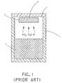
- FIG. 1A schematic diagram of the conventional PVT arrangement is shown in FIG. 1 .
- growthis carried out in a graphite crucible 1 sealed with a graphite lid 2 and loaded with a sublimation source 3 and a seed 4 .
- a polycrystalline SiC source 3is disposed at the bottom of the crucible 1 and a SiC seed 4 at the top of crucible 1 .
- the seed 4is often mounted directly to the crucible lid 2 using adhesives or other suitable means.
- Crucible 1is heated to a growth temperature, generally between 2000° C.
- source 3vaporizes and fills crucible 1 with volatile molecular species of Si 2 C, SiC 2 and Si.
- the temperature of source 3is maintained higher than the temperature of the seed 4 . This temperature difference forces the vapors from source 3 to migrate and precipitate on seed 4 forming a single crystal 5 .
- PVT growthis carried out under a small pressure of inert gas, generally between several and 200 Torr.
- graphiteIt is known that the permeability of graphite depends on the nature of the gas diffusing through graphite. Graphite is generally permeable to inert gases, hydrogen and nitrogen, but has a much lower permeability to the elements that form stable carbides. Accordingly, graphite has a very low permeability to the vapors formed during sublimation of silicon carbide, such as Si, Si 2 C and SiC 2 . Therefore, conventional PVT can be viewed as a “closed” process, in which the Si-bearing vapors practically do not leave the growth crucible, except small unintentional losses that can occur through the joint between the crucible body 1 and lid 2 .
- SiC single crystalshave also been grown using “open” processes, where a deliberate gas flow was established between the crucible interior and exterior. Examples include High Temperature Chemical Vapor Deposition (HTCVD), Halide Chemical Vapor Deposition (HCVD) and some PVT modifications.
- HTCVDHigh Temperature Chemical Vapor Deposition
- HCVDHalide Chemical Vapor Deposition
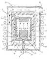
- FIG. 2A generalized diagram of the open SiC growth process is shown in FIG. 2 .
- the open processis carried out in a graphite crucible 1 , wherein source 3 is disposed at the crucible bottom and seed 4 is disposed at the crucible top.
- Graphite crucible 1 used in the open processis provided with a gas inlet 7 and gas outlet(s) 9 .
- a gas mixture 6that may contain Si precursors, C precursors, dopants and other gaseous components, enters the crucible through an inlet 7 .
- the reactantsundergo chemical transformations in a reaction zone 8 .
- the gaseous reaction productsblend with the vapors originating from solid source 3 and move toward seed 4 , where they precipitate on seed 4 and form single crystal 5 .
- Gaseous byproductsescape through gas outlet(s) 9 .
- the silicon and carbon precursorsare delivered to the reaction zone 8 in the form of silicon tetrachloride (SiCl 4 ) and propane (C 3 H 8 ) mixed with a large excess of hydrogen.
- SiCl 4silicon tetrachloride
- propaneC 3 H 8
- Graphiteis widely utilized in SiC sublimation growth as a material for crucibles, seed-holders, heat shields and other parts.
- the starting materials used in graphite manufacturingcontain boron. Therefore, boron is always present in graphite, where its atoms are chemically bound to carbon.
- High-temperature treatment under a halogen-containing atmosphereis widely used by graphite manufacturers for purification. During purification, the halogen molecules penetrate the graphite bulk, react with various impurities and form volatile halides with them. Driven by the concentration gradient, the halide molecules diffuse from the graphite bulk toward the surface, where they are removed by the flow of the carrier gas. Typically, removal of metallic impurities from graphite is more efficient than removal of boron.
- graphite manufacturerscharacterize graphite purity by the “ash content”, i.e., the amount of ash that remains after a graphite specimen is burnt in oxygen.
- the best-purity commercially available graphitecontains between 5 and 20 ppm of ash by weight. Boron forms volatile oxide upon burning in oxygen; therefore, graphite manufacturers seldom specify boron content in graphite.
- Impurity analyses using Glow Discharge Mass Spectroscopy (GDMS)show that the boron content even in the lowest-ash graphite is, typically, above 0.2 ppm and, in some cases, up to 1 ppm.
- Furnaces used for graphite purificationare, typically, very large and capable of accommodating metric tons of graphite. Cross-contamination between different items in a large graphite batch and contamination from the furnace itself limit the purification efficiency. As a result of the above limitations, graphite with a boron content below 0.1 ppm by weight is not readily available on a regular commercial basis.
- SiC sublimation growthutilizes crucibles, seed-holders, heat shields and other parts made of graphite.
- graphitecontains detectable levels of boron impurity, which can contaminate the growing crystal.
- SiC sublimation growthis carried out in the presence of dynamic reactive atmosphere comprised of an inert carrier gas and at least one reactive gas. The flow of reactive gas is supplied into the graphite growth crucible through an inlet port, and it escapes the crucible by filtering out across the permeable crucible wall.
- the main reactive component of the gas mixtureis a halosilane gas, desirably tetrahalosilane, such as tetrachlorosilane (SiCl 4 ) or tetrafluorosilane (SiF 4 ).
- the halosilane additiveis added in concentrations between 0.1 and 10% by volume and, more desirably, between 1 and 5%.
- the halosilaneundergoes pyrolysis forming lower halosilanes, such as SiCl 3 and SiCl 2 .
- the products of pyrolysisreact with boron forming volatile boron halides, such as BCl, BCl 2 and BCl 3 .
- the boron-containing byproductsare removed from the interior of the growth crucible by the flow of the gas mixture, which passes across (through) the permeable crucible wall.
- the gas mixturecan include small amounts of hydrogen, desirably between 0.1 to 3% by volume. The presence of hydrogen shifts the thermodynamic equilibrium in the gas phase in such a fashion that chemical attack on the SiC source and crystal is reduced.
- the grown crystalsare characterized by the concentration of unintentional boron acceptor below 7 ⁇ 10 15 cm ⁇ 3 and resistivity above 10 7 Ohm ⁇ cm.
- a crystal growth method in accordance with one non-limiting embodimentincludes (a) providing an enclosed growth crucible inside of a growth chamber with a thermal insulation disposed therebetween, the growth crucible having polycrystalline source material and a seed crystal disposed in spaced relation therein; (b) heating the interior of the growth crucible such that a temperature gradient forms between the source material and the seed crystal, the source material is heated to a sublimation temperature and the temperature gradient is sufficient to cause sublimated source material to be transported to the seed crystal where the sublimated source material precipitates on the seed crystal; and (c) causing a gas mixture to flow into the growth crucible and between the polycrystalline source material and an interior surface of the growth crucible, whereupon the gas mixture reacts with an unwanted element in the body of the growth crucible to form a gaseous byproduct which flows through the growth crucible to the exterior of the growth crucible, which is formed of a material that is permeable to the gas mixture and the gaseous byproduct, under the influence of the flow of the
- the inert gascan be either argon or helium.
- the halosilane gascan be tetrahalosilane in a concentration in the gas mixture between either 0.1% and 10% by volume, or between 1% and 5% by volume.
- the gas mixturecan further include hydrogen.
- the concentration of hydrogen in the gas mixturecan be between 0.1% and 3% by volume.
- the polycrystalline source materialcan be disposed in a source crucible which is disposed inside the growth crucible in spaced relation to interior surfaces of the growth crucible.
- An exterior of a base of the source cruciblecan be disposed in spaced relation to an interior of a floor of the growth crucible, thereby defining a first gap therebetween.
- An exterior of a wall of the source cruciblecan be disposed in spaced relation to an interior of a wall of the growth crucible, thereby defining a second gap therebetween.
- the gas mixturecan flow in the first and second gaps.
- the flow of the gas mixturecan be between 20 and 200 sccm.
- the wall(s) of the growth cruciblecan have a thickness that is between either 4 mm and 20 mm, or between 8 mm and 16 mm.
- the growth cruciblecan be made from graphite.
- the growth chambercan be made from fused silica.
- the thermal insulationcan be made from a porous graphite.
- the source material and the seed crystalcan both be made from SiC.
- a crystal growth method in accordance with another non-limiting embodimentcomprises (a) providing a seed crystal and a source material in spaced relation inside of a growth crucible is made from a material that is at least in-part gas permeable and which includes an element in the body thereof that is not wanted in a crystal grown in the growth crucible; (b) heating the growth chamber whereupon the source material sublimates and is transported via a temperature gradient in the growth chamber to the seed crystal where the sublimated source material precipitates; and (c) concurrent with step (b), causing a gas mixture to flow inside the growth crucible in a manner whereupon the unwanted element reacts with the gas mixture and is transported to the exterior of the growth crucible via the at-least gas permeable part thereof.
- the gas mixturecan flow through the growth crucible at a rate between 20 standard cubic centimeters per minute (sccm) and 200 sccm.
- the source materialcan be disposed in a source crucible that is positioned inside the growth crucible.
- the exterior wall of the source cruciblecan be spaced from an interior wall of the growth crucible.
- the spacecan be between 4 mm and 7 mm.
- the unwanted elementcan be boron.
- the gas mixturecan be a combination of (a) halosilane gas and (b) an inert gas.
- the growth cruciblecan be comprised of graphite.
- the source material and the seed crystalcan comprise SiC.
- FIG. 1is a schematic diagram of a prior art, closed physical vapor transport sublimation growth system
- FIG. 2is a schematic diagram of a prior art, open physical vapor transport sublimation growth system
- FIG. 3is a physical vapor transport sublimation growth system for the removal of boron in accordance with the embodiment described herein.
- SiC sublimation growthis conducted under a dynamic reactive atmosphere containing halogen.
- Halogenconverts boron, whether free or chemically bound, into volatile boron halides that are removed from the interior of the growth crucible by the flow of inert carrier gas filtering across the permeable crucible wall.
- crucible 1 and lid 2are made of high-density, fine-grain and low-porosity graphite, such as “ATJ” available from Union Carbide Corporation of Danbury, Conn., under registered trademark UCAR® (registration number 1008278), or similar.
- Growth crucible 1is loaded with a SiC polycrystalline source 3 and a seed crystal 4 .
- Source 3is disposed in a lower portion of the crucible 1 while seed 4 is disposed at the top of the crucible, desirably attached to crucible lid 2 , as shown in FIG. 3 .
- Source 3is contained in a thin-walled graphite source crucible 3 a , which rests on a graphite pedestal 3 b .
- the dimensions of growth crucible 1 , source crucible 3 a and pedestal 3 bare such that a gap 10 exists between the wall of the source crucible 3 a and the wall of the growth crucible 1 . Desirably, this gap is between 4 and 7 mm wide.
- Growth crucible 1loaded with source 3 and seed crystal 4 , is placed inside a chamber 20 of the growth station, where it is surrounded by a thermal insulation 12 .
- Thermal insulation 12is made of lightweight fibrous graphite, such as graphite felt or foam.
- the growth stationincludes a means for heating crucible 1 to a growth temperature.
- the chamber 20is water-cooled and is made of fused silica, and the heating means is realized by an exterior RF coil 23 .
- Metal chambers with resistive heaters or RF coils located inside the chambercan also or alternatively be utilized.
- crucible 1In order to initiate sublimation growth, crucible 1 is heated to the growth temperature, desirably between 2000° C. and 2400° C. At the growth temperature, SiC source 3 sublimes and fills the interior of the crucible 1 with vapor including Si, Si 2 C and SiC 2 volatile molecules. During growth, the temperature of source 3 is kept higher than the temperature of seed crystal 4 . This results in vapor transport in the direction from source 3 to seed crystal 4 . After reaching seed crystal 4 , the vapors condense thereon causing growth of a SiC single crystal 5 on seed crystal 4 .
- a gas mixture 6is supplied into growth crucible 1 by passing first through an inlet 21 of chamber 20 and then through an inlet port 7 of crucible 1 . After entering growth crucible 1 , gas mixture 6 flows through windows W in pedestal 3 b and in the gap 10 formed between walls of growth crucible 1 and the source crucible 3 a , as shown in FIG. 3 .
- Gas mixture 6 supplied into growth crucible 1is comprised of an inert carrier gas, desirably argon or helium, and one or more reactive gaseous additives.
- the main reactive additiveis a halosilane gas, desirably tetrahalosilane (SiCl 4 or SiF 4 ).
- the concentration of halosilane in the gas mixtureis desirably between 0.1 and 10% by volume, and more desirably between 1 and 5%.
- the gas mixturemay contain another reactive gaseous additive, such as hydrogen.
- the concentration of hydrogenis desirably between 0.1 and 3% by volume.
- the halosilane gasreacts with boron and converts it into volatile boron halides.
- These gaseous boron byproductsare removed from the interior of the crucible 1 by filtering through the permeable wall of the crucible 1 . Thereafter, these byproducts are removed from growth chamber 20 through an outlet port 22 by the flow of gas mixture 6 into growth chamber 20 .
- boron in the conditions of SiC sublimation growthis not exactly known. It is assumed that at high temperatures and in the presence of carbon and SiC, boron can be either in the form of elemental boron vapor, or in the form of a chemical compound with carbon, or in the form of a chemical compound with silicon. It is commonly believed that boron contained in graphite bulk is chemically bound to carbon and forms chemical bonds similar to those of boron carbide, B 4 C.
- the halosilane additiveundergoes pyrolysis. Pyrolysis of tetrahalosilane produces lower halosilanes.
- the main products of SiCl 4 pyrolysisare SiCl 2 and SiCl 3 .
- Thermodynamic analysisshows that, independently of the chemical form of boron, whether elementally or chemically bound to carbon or silicon, the lower halosilanes would react with boron-containing molecules and produce volatile boron halides, such as BCl, BCl 2 and BCl 3 .
- arrows 11symbolize the removal of boron halide products with the flow of carrier gas 6 passing across the crucible wall.
- halosilane reactive additiveis in its ability to react with boron contained in the bulk of graphite. While filtering across the crucible wall, carrier gas 6 delivers the products of halosilane pyrolysis into the graphite bulk, where they react with boron chemically bound to carbon. The flow of inert carrier gas 6 across the crucible wall facilitates the removal of volatile boron halides to the exterior of growth crucible 1 .
- halosilane pyrolysiscan attack SiC source 3 and growing crystal 5 .
- higher halosilane SiCl 3can attack SiC leading to the appearance of free carbon and lower halosilane SiCl 2 .
- This processcan lead to removal of silicon from growth crucible 1 , depletion of the SiC source 3 by silicon, and erosion of the SiC crystal 5 .
- the gas mixture supplied into crucible 1contains a small amount of hydrogen.
- the presence of hydrogen in the gas phaseleads to the appearance of small quantities of hydrogen halides (HCl in the case of SiCl 4 and HF in the case of SiF 4 ) and shifts the thermodynamic equilibrium in such a fashion that chemical attack on the SiC source 3 and crystal 5 is greatly reduced.
- the amount of hydrogen in the gas mixtureis desirably between 0.1 to 3% by volume.
- the flow of gas mixture 6is desirably between 20 sccm and 200 sccm. Too high of a flow can create a harmful overpressure inside crucible 1 and/or disturb the growth process, while too low of a flow can be ineffective or lead to the escape of Si-bearing vapors through the inlet port 7 of crucible 1 .
- the crucible wallshould be thin enough to allow efficient escape of the volatile boron halides by filtering/diffusion. At the same time, the crucible wall must not be too thin, otherwise, it may become transparent to the silicon-bearing vapors such as SiC 2 , Si 2 C and Si and cause Si losses from the crystal growth source 3 . Desirably, the thickness of the graphite crucible wall is desirably between 4 mm and 20 mm and, more desirably, between 8 mm and 16 mm.
- a reactive gas mixtureis supplied into the growth crucible through an inlet port, and it escapes the crucible by filtering out through the permeable crucible wall.
- the gas mixtureis comprised of an inert carrier gas and a halosilane gas, desirably SiCl 4 or SiF 4 , added in quantities between 0.1 and 10% by volume, and more desirably between 1 and 5%. Even more desirably, a small amount of hydrogen is added to the gas mixture in concentrations between 0.1 and 3% by volume. At high temperatures, the halosilane additive undergoes pyrolysis.
- the pyrolysis productsreact with boron, including boron residing in graphite.
- volatile boron halidesare produced.
- theyare removed from the growth crucible by filtering out across the permeable crucible wall, assisted by the flow of carrier gas.
- the hydrogen additivereduces the chemical attack of the SiC source and crystal and losses of silicon from the growth crucible.
- the grown crystal 5has a concentration of unintentional boron acceptor below 7 ⁇ 10 15 cm ⁇ 3 and resistivity above 10 7 Ohm ⁇ cm.
Landscapes
- Chemical & Material Sciences (AREA)
- Engineering & Computer Science (AREA)
- Crystallography & Structural Chemistry (AREA)
- Materials Engineering (AREA)
- Metallurgy (AREA)
- Organic Chemistry (AREA)
- Inorganic Chemistry (AREA)
- Crystals, And After-Treatments Of Crystals (AREA)
Abstract
Description
- A process for sublimation growth of SiC single crystals, in which growth is carried out under dynamic reactive atmosphere.
- The use of a reactive atmosphere for SiC sublimation growth comprised of an inert carrier gas, desirably, pure argon or helium, mixed with reactive gas additives.
- The use of a reactive gas additive comprising a halosilane, desirably SiCl4or SiF4.
- The use of a reactive atmosphere for SiC sublimation growth, which includes a combination of halosilane and hydrogen.
- The use of a reactive atmosphere for SiC sublimation growth, in which the concentration of halosilane is desirably between 0.1 and 10% by volume, and more desirably between 1 and 5% by volume.
- The use of a reactive atmosphere for SiC sublimation growth, in which the concentration of hydrogen is desirably between 0.1 and 3% by volume.
- A process of PVT sublimation growth under a continuous flow of a reactive gas mixture, in which the reactive gas mixture enters the growth crucible through an inlet port and escapes the crucible by filtering across the permeable crucible wall.
- A process of PVT sublimation growth under continuous flow of a reactive gas mixture, where the flow rate of the gas mixture is desirably between 10 sccm and 200 sccm, and more desirably between 20 sccm and 100 sccm.
- A growth crucible made of dense, fine-grain and low-porosity graphite having the wall desirably between 4 mm and 20 mm thick, and more desirably between 8 mm and 16 mm thick.
- A SiC sublimation growth process, in which the SiC source is contained in a thin-walled crucible disposed inside the growth crucible in such a fashion that a gap exists between the base and wall of the growth crucible and the base and wall of the source crucible. The gap between the walls of the growth crucible and the source crucible is desirably between 2 mm and 10 mm wide, and more desirably between 4 mm and 7 mm wide.
- SiC single crystals of 4H, 6H, 15R and 3C polytypes having unintentional boron acceptor in concentrations below 7·1015cm−3.
- Reduced concentration of unintentional boron acceptors in 6H and 4H SiC crystals;
- Higher and spatially more uniform resistivity in semi-insulating SiC crystals; and
- Higher yield of semi-insulating substrates per boule.
Claims (24)
Priority Applications (2)
| Application Number | Priority Date | Filing Date | Title |
|---|---|---|---|
| US11/900,242US8361227B2 (en) | 2006-09-26 | 2007-09-11 | Silicon carbide single crystals with low boron content |
| US13/471,866US8512471B2 (en) | 2006-04-11 | 2012-05-15 | Halosilane assisted PVT growth of SiC |
Applications Claiming Priority (3)
| Application Number | Priority Date | Filing Date | Title |
|---|---|---|---|
| US84731806P | 2006-09-26 | 2006-09-26 | |
| US11/784,971US8858709B1 (en) | 2006-04-11 | 2007-04-10 | Silicon carbide with low nitrogen content and method for preparation |
| US11/900,242US8361227B2 (en) | 2006-09-26 | 2007-09-11 | Silicon carbide single crystals with low boron content |
Related Parent Applications (1)
| Application Number | Title | Priority Date | Filing Date |
|---|---|---|---|
| US11/784,971Continuation-In-PartUS8858709B1 (en) | 2006-04-11 | 2007-04-10 | Silicon carbide with low nitrogen content and method for preparation |
Related Child Applications (1)
| Application Number | Title | Priority Date | Filing Date |
|---|---|---|---|
| US13/471,866ContinuationUS8512471B2 (en) | 2006-04-11 | 2012-05-15 | Halosilane assisted PVT growth of SiC |
Publications (2)
| Publication Number | Publication Date |
|---|---|
| US20080072817A1 US20080072817A1 (en) | 2008-03-27 |
| US8361227B2true US8361227B2 (en) | 2013-01-29 |
Family
ID=39223557
Family Applications (2)
| Application Number | Title | Priority Date | Filing Date |
|---|---|---|---|
| US11/900,242Active2031-05-28US8361227B2 (en) | 2006-04-11 | 2007-09-11 | Silicon carbide single crystals with low boron content |
| US13/471,866ActiveUS8512471B2 (en) | 2006-04-11 | 2012-05-15 | Halosilane assisted PVT growth of SiC |
Family Applications After (1)
| Application Number | Title | Priority Date | Filing Date |
|---|---|---|---|
| US13/471,866ActiveUS8512471B2 (en) | 2006-04-11 | 2012-05-15 | Halosilane assisted PVT growth of SiC |
Country Status (1)
| Country | Link |
|---|---|
| US (2) | US8361227B2 (en) |
Cited By (5)
| Publication number | Priority date | Publication date | Assignee | Title |
|---|---|---|---|---|
| US8858709B1 (en)* | 2006-04-11 | 2014-10-14 | Ii-Vi Incorporated | Silicon carbide with low nitrogen content and method for preparation |
| US9090989B2 (en) | 2012-05-24 | 2015-07-28 | Ii-Vi Incorporated | Vanadium compensated, SI SiC single crystals of NU and PI type and the crystal growth process thereof |
| US20160060514A1 (en)* | 2012-09-04 | 2016-03-03 | El-Seed Corporation | SiC FLUORESCENT MATERIAL AND METHOD FOR MANUFACTURING THE SAME, AND LIGHT EMITTING ELEMENT |
| US9322110B2 (en) | 2013-02-21 | 2016-04-26 | Ii-Vi Incorporated | Vanadium doped SiC single crystals and method thereof |
| DE102021104875A1 (en) | 2020-03-02 | 2021-09-02 | Ii-Vi Delaware, Inc. | Vanadium-compensated 4H and 6H single crystals of optical quality |
Families Citing this family (44)
| Publication number | Priority date | Publication date | Assignee | Title |
|---|---|---|---|---|
| DE102009009614A1 (en)* | 2008-12-24 | 2010-07-01 | Sicrystal Ag | Producing a silicon carbide volume single crystal, comprises producing silicon carbide growth gas phase in crystal growing area of culture crucible and growing-off the silicon carbide volume single crystal from the gas phase by deposition |
| DE102009004751B4 (en)* | 2009-01-15 | 2012-08-09 | Sicrystal Ag | Thermally isolated assembly and method of making a SiC bulk single crystal |
| JP4964274B2 (en)* | 2009-06-02 | 2012-06-27 | ジャパンスーパークォーツ株式会社 | Quartz glass crucible lid, quartz glass crucible and method of handling the same |
| WO2011078628A2 (en)* | 2009-12-24 | 2011-06-30 | Lg Innotek Co., Ltd. | Heat treatment container for vacuum heat treatment apparatus |
| JP2012051760A (en)* | 2010-09-01 | 2012-03-15 | Bridgestone Corp | Method for producing silicon carbide single crystal |
| CN102534805B (en)* | 2010-12-14 | 2014-08-06 | 北京天科合达蓝光半导体有限公司 | Silicon carbide crystal annealing process |
| KR20120136219A (en)* | 2011-06-08 | 2012-12-18 | 엘지이노텍 주식회사 | Apparatus for fabricating ingot |
| KR20120138112A (en)* | 2011-06-14 | 2012-12-24 | 엘지이노텍 주식회사 | Apparatus for fabricating ingot |
| KR20120140151A (en) | 2011-06-20 | 2012-12-28 | 엘지이노텍 주식회사 | Apparatus for fabricating ingot |
| KR101854727B1 (en) | 2011-06-24 | 2018-05-04 | 엘지이노텍 주식회사 | Apparatus for fabricating ingot |
| US20130000552A1 (en)* | 2011-06-28 | 2013-01-03 | Nitride Solutions Inc. | Device and method for producing bulk single crystals |
| DE102011089501B4 (en)* | 2011-12-21 | 2013-10-10 | Freiberger Compound Materials Gmbh | Apparatus and method for vaporizing material from a molten metal |
| EP2657373A1 (en)* | 2012-04-23 | 2013-10-30 | Chung-Shan Institute of Science and Technology, Armaments, Bureau, Ministry of National Defense | Crucible for growing crystals |
| US10322936B2 (en) | 2013-05-02 | 2019-06-18 | Pallidus, Inc. | High purity polysilocarb materials, applications and processes |
| US9657409B2 (en) | 2013-05-02 | 2017-05-23 | Melior Innovations, Inc. | High purity SiOC and SiC, methods compositions and applications |
| US9919972B2 (en) | 2013-05-02 | 2018-03-20 | Melior Innovations, Inc. | Pressed and self sintered polymer derived SiC materials, applications and devices |
| US11091370B2 (en) | 2013-05-02 | 2021-08-17 | Pallidus, Inc. | Polysilocarb based silicon carbide materials, applications and devices |
| WO2015038398A1 (en) | 2013-09-04 | 2015-03-19 | Nitride Solutions, Inc. | Bulk diffusion crystal growth process |
| JP2016532629A (en)* | 2013-09-06 | 2016-10-20 | ジーティーエイティー コーポレーションGtat Corporation | Method and apparatus for producing bulk silicon carbide from silicon carbide precursor |
| JP6247566B2 (en)* | 2014-02-28 | 2017-12-13 | 東洋炭素株式会社 | Heat treatment container, heat treatment container assembly, and semiconductor device manufacturing apparatus |
| AT516081B1 (en)* | 2014-07-16 | 2018-02-15 | Lkr Leichtmetallkompetenzzentrum Ranshofen Gmbh | Method and device for cleaning a porous material |
| US9580837B2 (en)* | 2014-09-03 | 2017-02-28 | Ii-Vi Incorporated | Method for silicon carbide crystal growth by reacting elemental silicon vapor with a porous carbon solid source material |
| US20160168750A1 (en)* | 2014-12-10 | 2016-06-16 | National Chung Shan Institute Of Science And Technology | Method of producing high-purity carbide mold |
| CN114000197B (en) | 2015-09-24 | 2025-01-10 | 帕里杜斯有限公司 | Vapor deposition apparatus and technology using high-purity polymer-derived silicon carbide |
| CN115594508A (en) | 2017-03-29 | 2023-01-13 | 帕里杜斯有限公司(Us) | Silicon carbide spatial shape and method for forming spheroids |
| RU2671349C1 (en)* | 2017-12-20 | 2018-10-30 | Федеральное государственное автономное образовательное учреждение высшего образования "Санкт-Петербургский государственный электротехнический университет "ЛЭТИ" им. В.И. Ульянова (Ленина)" (СПбГЭТУ "ЛЭТИ") | Method of producing monocrystalline sic |
| WO2019246515A1 (en)* | 2018-06-22 | 2019-12-26 | Massachusetts Institute Of Technology | Systems and methods for growth of silicon carbide over a layer comprising graphene and/or hexagonal boron nitride and related articles |
| CN108588817A (en)* | 2018-08-02 | 2018-09-28 | 山东大学 | A kind of growing method for growing crucible and SiC single crystal close to equilibrium state SiC single crystal |
| JP7268299B2 (en)* | 2018-08-08 | 2023-05-08 | 株式会社レゾナック | Shielding member and single crystal growth apparatus |
| CN109234798B (en)* | 2018-11-02 | 2019-07-23 | 山东天岳先进材料科技有限公司 | The continuous long crystal method of single-crystal silicon carbide |
| CN109881252A (en)* | 2019-04-08 | 2019-06-14 | 苏州优晶光电科技有限公司 | A kind of long crystal method of electric-resistivity method silicon carbide |
| KR102340110B1 (en)* | 2019-10-29 | 2021-12-17 | 주식회사 쎄닉 | Silicon carbide ingot, wafer and manufacturing method of the same |
| CN111088525B (en)* | 2019-12-26 | 2021-03-19 | 山东天岳先进科技股份有限公司 | Device for preparing single crystal and method for preparing silicon carbide single crystal |
| RU2736814C1 (en)* | 2020-04-03 | 2020-11-20 | Федеральное государственное автономное образовательное учреждение высшего образования "Санкт-Петербургский государственный электротехнический университет "ЛЭТИ" им. В.И. Ульянова (Ленина)" | Method of producing monocrystalline sic |
| CN111455457B (en)* | 2020-04-29 | 2021-09-21 | 金华博蓝特电子材料有限公司 | Silicon carbide crystal growth device and preparation method thereof |
| CN111534854B (en)* | 2020-06-12 | 2021-07-13 | 北京北方华创微电子装备有限公司 | Crystal growing furnace |
| CN112160028B (en)* | 2020-09-28 | 2021-08-13 | 中电化合物半导体有限公司 | Growth crucible and method capable of adjusting atmosphere of silicon carbide single crystal growth system |
| US20230407519A1 (en)* | 2020-11-19 | 2023-12-21 | Zadient Technologies SAS | Improved Furnace Apparatus for Crystal Production |
| EP4001475A1 (en)* | 2020-11-19 | 2022-05-25 | Zadient Technologies SAS | Improved furnace apparatus for crystal production |
| DE102020131840A1 (en)* | 2020-12-01 | 2022-06-02 | Friedrich-Alexander-Universität Erlangen-Nürnberg, Körperschaft des öffentlichen Rechts | PROCESS FOR PRODUCTION OF A SINGLE CRYSTAL IN A GROWTH CRUCIBLE |
| CN113502541A (en)* | 2021-06-21 | 2021-10-15 | 苏州优晶光电科技有限公司 | Silicon carbide crystal growth method and equipment for supplementing gaseous carbon source and silicon source |
| CN113774486B (en)* | 2021-09-01 | 2022-11-29 | 江苏超芯星半导体有限公司 | Crystal growth chamber and method for preparing silicon carbide by using same |
| DE102021123991B4 (en)* | 2021-09-16 | 2024-05-29 | Pva Tepla Ag | PVT process and equipment for the reliable production of single crystals |
| CN116254597A (en)* | 2023-03-22 | 2023-06-13 | 通威微电子有限公司 | Plasma doped silicon carbide crystal growing furnace |
Citations (9)
| Publication number | Priority date | Publication date | Assignee | Title |
|---|---|---|---|---|
| US3424628A (en)* | 1966-01-24 | 1969-01-28 | Western Electric Co | Methods and apparatus for treating semi-conductive materials with gases |
| US5611955A (en) | 1993-10-18 | 1997-03-18 | Northrop Grumman Corp. | High resistivity silicon carbide substrates for high power microwave devices |
| US5667587A (en) | 1996-12-18 | 1997-09-16 | Northrop Gruman Corporation | Apparatus for growing silicon carbide crystals |
| US5683507A (en) | 1995-09-05 | 1997-11-04 | Northrop Grumman Corporation | Apparatus for growing large silicon carbide single crystals |
| US5693565A (en)* | 1996-07-15 | 1997-12-02 | Dow Corning Corporation | Semiconductor chips suitable for known good die testing |
| US5746827A (en) | 1995-12-27 | 1998-05-05 | Northrop Grumman Corporation | Method of producing large diameter silicon carbide crystals |
| US6814801B2 (en) | 2002-06-24 | 2004-11-09 | Cree, Inc. | Method for producing semi-insulating resistivity in high purity silicon carbide crystals |
| US20060024439A2 (en)* | 2002-06-17 | 2006-02-02 | Asm International N.V. | System for controlling the sublimation of reactants |
| WO2006017074A2 (en)* | 2004-07-07 | 2006-02-16 | Ii-Vi Incorporated | Low-doped semi-insulating sic crystals and method |
Family Cites Families (8)
| Publication number | Priority date | Publication date | Assignee | Title |
|---|---|---|---|---|
| JP3491402B2 (en) | 1995-08-07 | 2004-01-26 | 株式会社デンソー | Single crystal manufacturing method and single crystal manufacturing apparatus |
| US6336971B1 (en) | 1997-09-12 | 2002-01-08 | Showa Denko Kabushiki Kaisha | Method and apparatus for producing silicon carbide single crystal |
| DE50004010D1 (en) | 1999-07-07 | 2003-11-13 | Siemens Ag | METHOD FOR SUBLIMATION GROWING A SIC SINGLE CRYSTAL WITH HEATING UNDER GROWING PRESSURE |
| EP1200650B1 (en) | 1999-07-07 | 2003-04-09 | Siemens Aktiengesellschaft | Sic monocrystal sublimation growth device with a film-covered crucible |
| FR2839730B1 (en)* | 2002-05-15 | 2004-08-27 | Centre Nat Rech Scient | SINGLE CRYSTAL SILICON CARBIDE FORMATION |
| US7601441B2 (en) | 2002-06-24 | 2009-10-13 | Cree, Inc. | One hundred millimeter high purity semi-insulating single crystal silicon carbide wafer |
| DE10335538A1 (en) | 2003-07-31 | 2005-02-24 | Sicrystal Ag | Process and apparatus for AIN single crystal production with gas permeable crucible wall |
| US8163086B2 (en) | 2007-08-29 | 2012-04-24 | Cree, Inc. | Halogen assisted physical vapor transport method for silicon carbide growth |
- 2007
- 2007-09-11USUS11/900,242patent/US8361227B2/enactiveActive
- 2012
- 2012-05-15USUS13/471,866patent/US8512471B2/enactiveActive
Patent Citations (9)
| Publication number | Priority date | Publication date | Assignee | Title |
|---|---|---|---|---|
| US3424628A (en)* | 1966-01-24 | 1969-01-28 | Western Electric Co | Methods and apparatus for treating semi-conductive materials with gases |
| US5611955A (en) | 1993-10-18 | 1997-03-18 | Northrop Grumman Corp. | High resistivity silicon carbide substrates for high power microwave devices |
| US5683507A (en) | 1995-09-05 | 1997-11-04 | Northrop Grumman Corporation | Apparatus for growing large silicon carbide single crystals |
| US5746827A (en) | 1995-12-27 | 1998-05-05 | Northrop Grumman Corporation | Method of producing large diameter silicon carbide crystals |
| US5693565A (en)* | 1996-07-15 | 1997-12-02 | Dow Corning Corporation | Semiconductor chips suitable for known good die testing |
| US5667587A (en) | 1996-12-18 | 1997-09-16 | Northrop Gruman Corporation | Apparatus for growing silicon carbide crystals |
| US20060024439A2 (en)* | 2002-06-17 | 2006-02-02 | Asm International N.V. | System for controlling the sublimation of reactants |
| US6814801B2 (en) | 2002-06-24 | 2004-11-09 | Cree, Inc. | Method for producing semi-insulating resistivity in high purity silicon carbide crystals |
| WO2006017074A2 (en)* | 2004-07-07 | 2006-02-16 | Ii-Vi Incorporated | Low-doped semi-insulating sic crystals and method |
Non-Patent Citations (8)
| Title |
|---|
| A. Elison et al.; "SiC Crystal Growth by HTCVD", Mat. Sci. Forum, vols. 457-460 (2004) pp. 9-14. |
| G.F. Hewitt; Chemistry and Physics of Carbon-A Series of Advances; Edited by Philip L. Walker, Jr.; vol. 1; Copyright 1965 by Marcel Dekker, Inc. New York; pp. 73-119. |
| M. Fanton et al.; "Growth of Bulk SiC by Halide Chemical Vapor Deposition", Mat. Sci. Forum, vols. 457-460 (2004) pp. 87-90. |
| M.A. Fanton et al.; "Growth of SiC Boules With Low Boron Concentration"; Materials Science Forum, vols. 527-529 (2006). |
| Machine translation of EP 1567696, Rasp et al Jul. 2004.* |
| Machine translation of EP1567696B1, Rasp et al.* |
| P. Wellman et al.; "Modified Physical Vapor Transport Growth of SiC-Control of Gas Phase Composition for Improved process Condition", Mat. Sci. Forum, vols. 483-485 (2005) pp. 25-30. |
| Y. M. Tairov and V. F. Tsvetkov; "Investigation of Growth Processes of Ingots of Silicon Carbide Single Crystals", Journal of Crystal Growth, vol. 43 (1978) pp. 209-212. |
Cited By (8)
| Publication number | Priority date | Publication date | Assignee | Title |
|---|---|---|---|---|
| US8858709B1 (en)* | 2006-04-11 | 2014-10-14 | Ii-Vi Incorporated | Silicon carbide with low nitrogen content and method for preparation |
| US9090989B2 (en) | 2012-05-24 | 2015-07-28 | Ii-Vi Incorporated | Vanadium compensated, SI SiC single crystals of NU and PI type and the crystal growth process thereof |
| USRE48378E1 (en) | 2012-05-24 | 2021-01-05 | Ii-Vi Delaware, Inc. | Vanadium compensated, SI SiC single crystals of NU and PI type and the crystal growth process thereof |
| US20160060514A1 (en)* | 2012-09-04 | 2016-03-03 | El-Seed Corporation | SiC FLUORESCENT MATERIAL AND METHOD FOR MANUFACTURING THE SAME, AND LIGHT EMITTING ELEMENT |
| US9322110B2 (en) | 2013-02-21 | 2016-04-26 | Ii-Vi Incorporated | Vanadium doped SiC single crystals and method thereof |
| DE102021104875A1 (en) | 2020-03-02 | 2021-09-02 | Ii-Vi Delaware, Inc. | Vanadium-compensated 4H and 6H single crystals of optical quality |
| DE102021003909A1 (en) | 2020-03-02 | 2021-09-16 | Ii-Vi Delaware, Inc. | VANADIUM COMPENSATED 4H AND 6H SINGLE CRYSTALS OF OPTICAL QUALITY AND SILICON CARBIDE CRYSTALS AND METHOD OF MANUFACTURING THE SAME |
| DE102021004531A1 (en) | 2020-03-02 | 2021-11-04 | Ii-Vi Delaware, Inc. | VANADIUM COMPENSATED 4H AND 6H SINGLE CRYSTALS OF OPTICAL QUALITY |
Also Published As
| Publication number | Publication date |
|---|---|
| US8512471B2 (en) | 2013-08-20 |
| US20080072817A1 (en) | 2008-03-27 |
| US20120225004A1 (en) | 2012-09-06 |
Similar Documents
| Publication | Publication Date | Title |
|---|---|---|
| US8361227B2 (en) | Silicon carbide single crystals with low boron content | |
| US9322110B2 (en) | Vanadium doped SiC single crystals and method thereof | |
| USRE48378E1 (en) | Vanadium compensated, SI SiC single crystals of NU and PI type and the crystal growth process thereof | |
| US8858709B1 (en) | Silicon carbide with low nitrogen content and method for preparation | |
| US20220049373A1 (en) | Sic single crystal(s) doped from gas phase | |
| JPH05208900A (en) | Apparatus for growing silicon carbide single crystal | |
| US12237377B2 (en) | SiC semiconductor substrate, and, production method therefor and production device therefor | |
| JP4387159B2 (en) | Graphite material, carbon fiber reinforced carbon composite material, and expanded graphite sheet | |
| US9580837B2 (en) | Method for silicon carbide crystal growth by reacting elemental silicon vapor with a porous carbon solid source material | |
| KR101031407B1 (en) | Formation method of single crystal silicon carbide | |
| US9447517B2 (en) | Seed material for liquid phase epitaxial growth of monocrystalline silicon carbide, and method for liquid phase epitaxial growth of monocrystalline silicon | |
| EP2383373A1 (en) | Apparatus for producing nitride semiconductor crystal, method for producing nitride semiconductor crystal, and nitride semiconductor crystal | |
| US20160284545A1 (en) | System and method for producing polycrystalline group iii nitride articles and use thereof in production of single crystal group iii nitride articles | |
| JP2007145679A (en) | Aluminum nitride single crystal manufacturing apparatus and manufacturing method thereof | |
| Hsiao et al. | Major Carrier Element Concentrations in SiC Powder and Bulk Crystal | |
| KR20070009567A (en) | Silicon carbide single crystal, silicon carbide single crystal wafer and method for manufacturing same | |
| JPH089517B2 (en) | Single crystal manufacturing method | |
| JPS5919917B2 (en) | epitaxial epitaxy |
Legal Events
| Date | Code | Title | Description |
|---|---|---|---|
| AS | Assignment | Owner name:II-VI INCORPORATED, PENNSYLVANIA Free format text:ASSIGNMENT OF ASSIGNORS INTEREST;ASSIGNORS:ZWIEBACK, ILYA;ANDERSON, THOMAS E.;GUPTA, AVINASH K.;REEL/FRAME:019852/0364 Effective date:20070907 | |
| STCF | Information on status: patent grant | Free format text:PATENTED CASE | |
| FPAY | Fee payment | Year of fee payment:4 | |
| AS | Assignment | Owner name:BANK OF AMERICA, N.A., AS ADMINISTRATIVE AGENT, NO Free format text:NOTICE OF GRANT OF SECURITY INTEREST IN PATENTS;ASSIGNORS:II-VI INCORPORATED;MARLOW INDUSTRIES, INC.;EPIWORKS, INC.;AND OTHERS;REEL/FRAME:050484/0204 Effective date:20190924 Owner name:BANK OF AMERICA, N.A., AS ADMINISTRATIVE AGENT, NORTH CAROLINA Free format text:NOTICE OF GRANT OF SECURITY INTEREST IN PATENTS;ASSIGNORS:II-VI INCORPORATED;MARLOW INDUSTRIES, INC.;EPIWORKS, INC.;AND OTHERS;REEL/FRAME:050484/0204 Effective date:20190924 | |
| AS | Assignment | Owner name:II-VI DELAWARE, INC., DELAWARE Free format text:ASSIGNMENT OF ASSIGNORS INTEREST;ASSIGNOR:II-VI INCORPORATED;REEL/FRAME:051210/0411 Effective date:20191202 | |
| MAFP | Maintenance fee payment | Free format text:PAYMENT OF MAINTENANCE FEE, 8TH YEAR, LARGE ENTITY (ORIGINAL EVENT CODE: M1552); ENTITY STATUS OF PATENT OWNER: LARGE ENTITY Year of fee payment:8 | |
| AS | Assignment | Owner name:JPMORGAN CHASE BANK, N.A., AS COLLATERAL AGENT, NEW YORK Free format text:SECURITY INTEREST;ASSIGNORS:II-VI INCORPORATED;II-VI DELAWARE, INC.;M CUBED TECHNOLOGIES, INC.;AND OTHERS;REEL/FRAME:060562/0254 Effective date:20220701 | |
| AS | Assignment | Owner name:PHOTOP TECHNOLOGIES, INC., CALIFORNIA Free format text:PATENT RELEASE AND REASSIGNMENT;ASSIGNOR:BANK OF AMERICA, N.A., AS ADMINISTRATIVE AGENT;REEL/FRAME:060574/0001 Effective date:20220701 Owner name:II-VI OPTOELECTRONIC DEVICES, INC., NEW JERSEY Free format text:PATENT RELEASE AND REASSIGNMENT;ASSIGNOR:BANK OF AMERICA, N.A., AS ADMINISTRATIVE AGENT;REEL/FRAME:060574/0001 Effective date:20220701 Owner name:II-VI DELAWARE, INC., PENNSYLVANIA Free format text:PATENT RELEASE AND REASSIGNMENT;ASSIGNOR:BANK OF AMERICA, N.A., AS ADMINISTRATIVE AGENT;REEL/FRAME:060574/0001 Effective date:20220701 Owner name:II-VI PHOTONICS (US), INC., MASSACHUSETTS Free format text:PATENT RELEASE AND REASSIGNMENT;ASSIGNOR:BANK OF AMERICA, N.A., AS ADMINISTRATIVE AGENT;REEL/FRAME:060574/0001 Effective date:20220701 Owner name:M CUBED TECHNOLOGIES, INC., CONNECTICUT Free format text:PATENT RELEASE AND REASSIGNMENT;ASSIGNOR:BANK OF AMERICA, N.A., AS ADMINISTRATIVE AGENT;REEL/FRAME:060574/0001 Effective date:20220701 Owner name:II-VI OPTICAL SYSTEMS, INC., CALIFORNIA Free format text:PATENT RELEASE AND REASSIGNMENT;ASSIGNOR:BANK OF AMERICA, N.A., AS ADMINISTRATIVE AGENT;REEL/FRAME:060574/0001 Effective date:20220701 Owner name:FINISAR CORPORATION, CALIFORNIA Free format text:PATENT RELEASE AND REASSIGNMENT;ASSIGNOR:BANK OF AMERICA, N.A., AS ADMINISTRATIVE AGENT;REEL/FRAME:060574/0001 Effective date:20220701 Owner name:OPTIUM CORPORATION, CALIFORNIA Free format text:PATENT RELEASE AND REASSIGNMENT;ASSIGNOR:BANK OF AMERICA, N.A., AS ADMINISTRATIVE AGENT;REEL/FRAME:060574/0001 Effective date:20220701 Owner name:COADNA PHOTONICS, INC., PENNSYLVANIA Free format text:PATENT RELEASE AND REASSIGNMENT;ASSIGNOR:BANK OF AMERICA, N.A., AS ADMINISTRATIVE AGENT;REEL/FRAME:060574/0001 Effective date:20220701 Owner name:KAILIGHT PHOTONICS, INC., CALIFORNIA Free format text:PATENT RELEASE AND REASSIGNMENT;ASSIGNOR:BANK OF AMERICA, N.A., AS ADMINISTRATIVE AGENT;REEL/FRAME:060574/0001 Effective date:20220701 Owner name:LIGHTSMYTH TECHNOLOGIES, INC., OREGON Free format text:PATENT RELEASE AND REASSIGNMENT;ASSIGNOR:BANK OF AMERICA, N.A., AS ADMINISTRATIVE AGENT;REEL/FRAME:060574/0001 Effective date:20220701 Owner name:EPIWORKS, INC., ILLINOIS Free format text:PATENT RELEASE AND REASSIGNMENT;ASSIGNOR:BANK OF AMERICA, N.A., AS ADMINISTRATIVE AGENT;REEL/FRAME:060574/0001 Effective date:20220701 Owner name:MARLOW INDUSTRIES, INC., TEXAS Free format text:PATENT RELEASE AND REASSIGNMENT;ASSIGNOR:BANK OF AMERICA, N.A., AS ADMINISTRATIVE AGENT;REEL/FRAME:060574/0001 Effective date:20220701 Owner name:II-VI INCORPORATED, PENNSYLVANIA Free format text:PATENT RELEASE AND REASSIGNMENT;ASSIGNOR:BANK OF AMERICA, N.A., AS ADMINISTRATIVE AGENT;REEL/FRAME:060574/0001 Effective date:20220701 | |
| AS | Assignment | Owner name:II-VI DELAWARE, INC., PENNSYLVANIA Free format text:PARTIAL TERMINATION AND RELEASE OF SECURITY INTEREST IN PATENTS;ASSIGNOR:JPMORGAN CHASE BANK, N.A.;REEL/FRAME:065773/0129 Effective date:20231204 | |
| AS | Assignment | Owner name:II-VI ADVANCED MATERIALS, LLC, NEW JERSEY Free format text:ASSIGNMENT OF ASSIGNORS INTEREST;ASSIGNOR:II-VI DELAWARE, INC.;REEL/FRAME:066106/0055 Effective date:20231124 | |
| MAFP | Maintenance fee payment | Free format text:PAYMENT OF MAINTENANCE FEE, 12TH YEAR, LARGE ENTITY (ORIGINAL EVENT CODE: M1553); ENTITY STATUS OF PATENT OWNER: LARGE ENTITY Year of fee payment:12 |