US8358266B2 - Light turning device with prismatic light turning features - Google Patents
Light turning device with prismatic light turning featuresDownload PDFInfo
- Publication number
- US8358266B2 US8358266B2US12/552,124US55212409AUS8358266B2US 8358266 B2US8358266 B2US 8358266B2US 55212409 AUS55212409 AUS 55212409AUS 8358266 B2US8358266 B2US 8358266B2
- Authority
- US
- United States
- Prior art keywords
- light
- slits
- guide body
- light guide
- display
- Prior art date
- Legal status (The legal status is an assumption and is not a legal conclusion. Google has not performed a legal analysis and makes no representation as to the accuracy of the status listed.)
- Expired - Fee Related, expires
Links
Images


Classifications
- G—PHYSICS
- G02—OPTICS
- G02B—OPTICAL ELEMENTS, SYSTEMS OR APPARATUS
- G02B6/00—Light guides; Structural details of arrangements comprising light guides and other optical elements, e.g. couplings
- G02B6/0001—Light guides; Structural details of arrangements comprising light guides and other optical elements, e.g. couplings specially adapted for lighting devices or systems
- G02B6/0011—Light guides; Structural details of arrangements comprising light guides and other optical elements, e.g. couplings specially adapted for lighting devices or systems the light guides being planar or of plate-like form
- G02B6/0065—Manufacturing aspects; Material aspects
- B—PERFORMING OPERATIONS; TRANSPORTING
- B29—WORKING OF PLASTICS; WORKING OF SUBSTANCES IN A PLASTIC STATE IN GENERAL
- B29D—PRODUCING PARTICULAR ARTICLES FROM PLASTICS OR FROM SUBSTANCES IN A PLASTIC STATE
- B29D11/00—Producing optical elements, e.g. lenses or prisms
- B29D11/00663—Production of light guides
- G—PHYSICS
- G02—OPTICS
- G02B—OPTICAL ELEMENTS, SYSTEMS OR APPARATUS
- G02B6/00—Light guides; Structural details of arrangements comprising light guides and other optical elements, e.g. couplings
- G02B6/0001—Light guides; Structural details of arrangements comprising light guides and other optical elements, e.g. couplings specially adapted for lighting devices or systems
- G02B6/0011—Light guides; Structural details of arrangements comprising light guides and other optical elements, e.g. couplings specially adapted for lighting devices or systems the light guides being planar or of plate-like form
- G02B6/0033—Means for improving the coupling-out of light from the light guide
- G02B6/0035—Means for improving the coupling-out of light from the light guide provided on the surface of the light guide or in the bulk of it
- G—PHYSICS
- G02—OPTICS
- G02B—OPTICAL ELEMENTS, SYSTEMS OR APPARATUS
- G02B6/00—Light guides; Structural details of arrangements comprising light guides and other optical elements, e.g. couplings
- G02B6/0001—Light guides; Structural details of arrangements comprising light guides and other optical elements, e.g. couplings specially adapted for lighting devices or systems
- G02B6/0011—Light guides; Structural details of arrangements comprising light guides and other optical elements, e.g. couplings specially adapted for lighting devices or systems the light guides being planar or of plate-like form
- G02B6/0013—Means for improving the coupling-in of light from the light source into the light guide
- G02B6/0015—Means for improving the coupling-in of light from the light source into the light guide provided on the surface of the light guide or in the bulk of it
- G—PHYSICS
- G02—OPTICS
- G02B—OPTICAL ELEMENTS, SYSTEMS OR APPARATUS
- G02B6/00—Light guides; Structural details of arrangements comprising light guides and other optical elements, e.g. couplings
- G02B6/0001—Light guides; Structural details of arrangements comprising light guides and other optical elements, e.g. couplings specially adapted for lighting devices or systems
- G02B6/0011—Light guides; Structural details of arrangements comprising light guides and other optical elements, e.g. couplings specially adapted for lighting devices or systems the light guides being planar or of plate-like form
- G02B6/0013—Means for improving the coupling-in of light from the light source into the light guide
- G02B6/0023—Means for improving the coupling-in of light from the light source into the light guide provided by one optical element, or plurality thereof, placed between the light guide and the light source, or around the light source
- G02B6/0028—Light guide, e.g. taper
Definitions
- This inventionrelates generally to light turning devices. More particularly, this invention relates to light turning devices utilizing prismatic structures to guide light to, for example, illuminate a display. This invention also relates to methods of use and fabrication of these devices.
- Microelectromechanical systemsinclude micro mechanical elements, actuators, and electronics. Micromechanical elements may be created using deposition, etching, and/or other micromachining processes that etch away parts of substrates and/or deposited material layers or that add layers to form electrical and electromechanical devices.
- MEMS deviceOne type of MEMS device is called an interferometric modulator.
- interferometric modulator or interferometric light modulatorrefers to a device that selectively absorbs and/or reflects light using the principles of optical interference.
- an interferometric modulatormay comprise a pair of conductive plates, one or both of which may be transparent and/or reflective in whole or part and capable of relative motion upon application of an appropriate electrical signal.
- one platemay comprise a stationary layer deposited on a substrate and the other plate may comprise a metallic membrane separated from the stationary layer by an air gap.
- the position of one plate in relation to anothercan change the optical interference of light incident on the interferometric modulator.
- Such deviceshave a wide range of applications, and it would be beneficial in the art to utilize and/or modify the characteristics of these types of devices so that their features can be exploited in improving existing products and creating new products that have not yet been developed.
- a light guide apparatuscomprising a light guide body formed of a light propagating material that supports the propagation of light through a length of the light guide body.
- the light guide bodyis defined by a plurality of exterior surfaces.
- a first of the exterior surfacescomprises a first plurality of spaced-apart slits configured to redirect light incident on the light guide body, with each slit formed by an undercut in the first exterior surface.
- a second of the exterior surfacescomprises a second plurality of spaced-apart slits configured to redirect light incident on the light guide body, with each slit formed by an undercut in the second exterior surface.
- an illumination apparatuscomprises a first means for generating light and directing the light to propagate through a light turning body; a second means for redirecting the light propagating through the light turning body; and a third means for redirecting the light propagating through the light turning body.
- a method for illuminationcomprises propagating light through a light turning body. Light propagating through the body is redirected by impinging the light on facets of a first and a second plurality of slits. The pluralities of slits are formed by undercuts in two surfaces of the light turning body.
- a method for manufacturing an illumination devicecomprises providing a body of light propagating material that supports the propagation of light through a length of the body. First and second pluralities of spaced-apart undercuts are formed in different sides of the body. In some other embodiments, the illumination device formed by this method is provided.
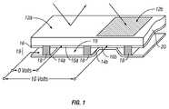
- FIG. 1is an isometric view depicting a portion of one embodiment of an interferometric modulator display in which a movable reflective layer of a first interferometric modulator is in a relaxed position and a movable reflective layer of a second interferometric modulator is in an actuated position.
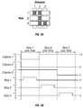
- FIG. 2is a system block diagram illustrating one embodiment of an electronic device incorporating a 3 ⁇ 3 interferometric modulator display.
- FIG. 3is a diagram of movable mirror position versus applied voltage for one exemplary embodiment of an interferometric modulator of FIG. 1 .
- FIG. 4is an illustration of a set of row and column voltages that may be used to drive an interferometric modulator display.
- FIG. 5Aillustrates one exemplary frame of display data in the 3 ⁇ 3 interferometric modulator display of FIG. 2 .
- FIG. 5Billustrates one exemplary timing diagram for row and column signals that may be used to write the frame of FIG. 5A .
- FIGS. 6A and 6Bare system block diagrams illustrating an embodiment of a visual display device comprising a plurality of interferometric modulators.
- FIG. 7Ais a cross section of the device of FIG. 1 .
- FIG. 7Bis a cross section of an alternative embodiment of an interferometric modulator.
- FIG. 7Cis a cross section of another alternative embodiment of an interferometric modulator.
- FIG. 7Dis a cross section of yet another alternative embodiment of an interferometric modulator.
- FIG. 7Eis a cross section of an additional alternative embodiment of an interferometric modulator.
- FIG. 8is a cross section of a display device.
- FIG. 9is an enlargement of a portion of the cross section of FIG. 8 .
- FIG. 10Ais a cross section of an embodiment of a light turning feature.
- FIG. 10Bis a cross section of another embodiment of a light turning feature.
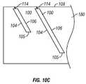
- FIG. 10Cis a cross section of yet another embodiment of a light turning feature.
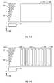
- FIG. 11Ais a top plan view of an embodiment of a display device.
- FIG. 11Bis a cross section of the display device of FIG. 11A .
- FIGS. 11C-11Eare top plan views of embodiments of display devices.
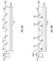
- FIGS. 12A-12Bare cross sections of embodiments of display devices.
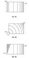
- FIGS. 13A-13Care top plan views of embodiments of display devices.
- the embodimentsmay be implemented in or associated with a variety of electronic devices such as, but not limited to, mobile telephones, wireless devices, personal data assistants (PDAs), hand-held or portable computers, GPS receivers/navigators, cameras, MP3 players, camcorders, game consoles, wrist watches, clocks, calculators, television monitors, flat panel displays, computer monitors, auto displays (e.g., odometer display, etc.), cockpit controls and/or displays, display of camera views (e.g., display of a rear view camera in a vehicle), electronic photographs, electronic billboards or signs, projectors, architectural structures, packaging, and aesthetic structures (e.g., display of images on a piece of jewelry).
- MEMS devices of similar structure to those described hereincan also be used in non-display applications such as in electronic switching devices.
- Some embodiments disclosed hereininclude a light guide having undercuts in the body of the light guide.
- the undercutsform prismatic features, also referred to as slits, that turn or redirect light propagating through the light guide body.
- the walls of the undercutsform facets that reflect light in a desired direction.
- a light sourceis connected to the light guide body. Light from the light source is injected into the light guide body, propagates through the body and contacts the facets of the undercuts. The facets of the slits redirect the light out of the light guide body, e.g., to a display formed of, e.g., interferometric modulators.
- first and second pluralities of slitsare provided on opposite major surfaces of the light guide body. The slits are configured to redirect the light out of a common major surface.
- a plurality of slitsis formed in a line light source.
- the slitsare positioned and angled to turn light injected into the line light source from a point light emitter at the end of the line light source.
- the turned lightcan, e.g., be expelled out of the line light source along the length of the light source or, in some other embodiments, to an area containing a second plurality of slits.
- the second plurality of slitscan turn the light towards a display.
- FIG. 1One interferometric modulator display embodiment comprising an interferometric MEMS display element is illustrated in FIG. 1 .
- the pixelsare in either a bright or dark state.
- the display elementIn the bright (“relaxed” or “open”) state, the display element reflects a large portion of incident visible light to a user.
- the dark (“actuated” or “closed”) stateWhen in the dark (“actuated” or “closed”) state, the display element reflects little incident visible light to the user.
- the light reflectance properties of the “on” and “off” statesmay be reversed.
- MEMS pixelscan be configured to reflect predominantly at selected colors, allowing for a color display in addition to black and white.
- FIG. 1is an isometric view depicting two adjacent pixels in a series of pixels of a visual display, wherein each pixel comprises a MEMS interferometric modulator.
- an interferometric modulator displaycomprises a row/column array of these interferometric modulators.
- Each interferometric modulatorincludes a pair of reflective layers positioned at a variable and controllable distance from each other to form a resonant optical gap with at least one variable dimension.
- one of the reflective layersmay be moved between two positions. In the first position, referred to herein as the relaxed position, the movable reflective layer is positioned at a relatively large distance from a fixed partially reflective layer.
- the movable reflective layerIn the second position, referred to herein as the actuated position, the movable reflective layer is positioned more closely adjacent to the partially reflective layer. Incident light that reflects from the two layers interferes constructively or destructively depending on the position of the movable reflective layer, producing either an overall reflective or non-reflective state for each pixel.
- the depicted portion of the pixel array in FIG. 1includes two adjacent interferometric modulators 12 a and 12 b .
- a movable reflective layer 14 ais illustrated in a relaxed position at a predetermined distance from an optical stack 16 a , which includes a partially reflective layer.
- the movable reflective layer 14 bis illustrated in an actuated position adjacent to the optical stack 16 b.
- optical stack 16typically comprise several fused layers, which can include an electrode layer, such as indium tin oxide (ITO), a partially reflective layer, such as chromium, and a transparent dielectric.
- ITOindium tin oxide
- the optical stack 16is thus electrically conductive, partially transparent and partially reflective, and may be fabricated, for example, by depositing one or more of the above layers onto a transparent substrate 20 .
- the partially reflective layercan be formed from a variety of materials that are partially reflective such as various metals, semiconductors, and dielectrics.
- the partially reflective layercan be formed of one or more layers of materials, and each of the layers can be formed of a single material or a combination of materials.
- the layers of the optical stack 16are patterned into parallel strips, and may form row electrodes in a display device as described further below.
- the movable reflective layers 14 a , 14 bmay be formed as a series of parallel strips of a deposited metal layer or layers (orthogonal to the row electrodes of 16 a , 16 b ) to form columns deposited on top of posts 18 and an intervening sacrificial material deposited between the posts 18 . When the sacrificial material is etched away, the movable reflective layers 14 a , 14 b are separated from the optical stacks 16 a , 16 b by a defined gap 19 .
- a highly conductive and reflective material such as aluminummay be used for the reflective layers 14 , and these strips may form column electrodes in a display device. Note that FIG. 1 may not be to scale. In some embodiments, the spacing between posts 18 may be on the order of 10-100 um, while the gap 19 may be on the order of ⁇ 1000 Angstroms.
- the gap 19remains between the movable reflective layer 14 a and optical stack 16 a , with the movable reflective layer 14 a in a mechanically relaxed state, as illustrated by the pixel 12 a in FIG. 1 .
- a potential (voltage) differenceis applied to a selected row and column, the capacitor formed at the intersection of the row and column electrodes at the corresponding pixel becomes charged, and electrostatic forces pull the electrodes together. If the voltage is high enough, the movable reflective layer 14 is deformed and is forced against the optical stack 16 .
- a dielectric layerwithin the optical stack 16 may prevent shorting and control the separation distance between layers 14 and 16 , as illustrated by actuated pixel 12 b on the right in FIG. 1 . The behavior is the same regardless of the polarity of the applied potential difference.
- FIGS. 2 through 5Billustrate one exemplary process and system for using an array of interferometric modulators in a display application.
- FIG. 2is a system block diagram illustrating one embodiment of an electronic device that may incorporate interferometric modulators.
- the electronic deviceincludes a processor 21 which may be any general purpose single- or multi-chip microprocessor such as an ARM®, Pentium®, 8051, MIPS®, Power PC®, or ALPHA®, or any special purpose microprocessor such as a digital signal processor, microcontroller, or a programmable gate array.
- the processor 21may be configured to execute one or more software modules.
- the processormay be configured to execute one or more software applications, including a web browser, a telephone application, an email program, or any other software application.
- the processor 21is also configured to communicate with an array driver 22 .
- the array driver 22includes a row driver circuit 24 and a column driver circuit 26 that provide signals to a display array or panel 30 .
- the cross section of the array illustrated in FIG. 1is shown by the lines 1 - 1 in FIG. 2 .
- FIG. 2illustrates a 3 ⁇ 3 array of interferometric modulators for the sake of clarity, the display array 30 may contain a very large number of interferometric modulators, and may have a different number of interferometric modulators in rows than in columns (e.g., 300 pixels per row by 190 pixels per column).
- FIG. 3is a diagram of movable mirror position versus applied voltage for one exemplary embodiment of an interferometric modulator of FIG. 1 .
- the row/column actuation protocolmay take advantage of a hysteresis property of these devices as illustrated in FIG. 3 .
- An interferometric modulatormay require, for example, a 10 volt potential difference to cause a movable layer to deform from the relaxed state to the actuated state. However, when the voltage is reduced from that value, the movable layer maintains its state as the voltage drops back below 10 volts. In the exemplary embodiment of FIG. 3 , the movable layer does not relax completely until the voltage drops below 2 volts.
- the row/column actuation protocolcan be designed such that during row strobing, pixels in the strobed row that are to be actuated are exposed to a voltage difference of about 10 volts, and pixels that are to be relaxed are exposed to a voltage difference of close to zero volts.
- each pixelsees a potential difference within the “stability window” of 3-7 volts in this example.
- This featuremakes the pixel design illustrated in FIG. 1 stable under the same applied voltage conditions in either an actuated or relaxed pre-existing state. Since each pixel of the interferometric modulator, whether in the actuated or relaxed state, is essentially a capacitor formed by the fixed and moving reflective layers, this stable state can be held at a voltage within the hysteresis window with almost no power dissipation. Essentially no current flows into the pixel if the applied potential is fixed.
- a frame of an imagemay be created by sending a set of data signals (each having a certain voltage level) across the set of column electrodes in accordance with the desired set of actuated pixels in the first row.
- a row pulseis then applied to a first row electrode, actuating the pixels corresponding to the set of data signals.
- the set of data signalsis then changed to correspond to the desired set of actuated pixels in a second row.
- a pulseis then applied to the second row electrode, actuating the appropriate pixels in the second row in accordance with the data signals.
- the first row of pixelsare unaffected by the second row pulse, and remain in the state they were set to during the first row pulse. This may be repeated for the entire series of rows in a sequential fashion to produce the frame.
- the framesare refreshed and/or updated with new image data by continually repeating this process at some desired number of frames per second.
- a wide variety of protocols for driving row and column electrodes of pixel arrays to produce image framesmay be used.
- FIGS. 4 and 5A and 5 Billustrate one possible actuation protocol for creating a display frame on the 3 ⁇ 3 array of FIG. 2 .
- FIG. 4illustrates a possible set of column and row voltage levels that may be used for pixels exhibiting the hysteresis curves of FIG. 3 .
- actuating a pixelinvolves setting the appropriate column to ⁇ V bias , and the appropriate row to + ⁇ V, which may correspond to ⁇ 5 volts and +5 volts respectively Relaxing the pixel is accomplished by setting the appropriate column to +V bias , and the appropriate row to the same + ⁇ V, producing a zero volt potential difference across the pixel.
- the pixelsare stable in whatever state they were originally in, regardless of whether the column is at +V bias , or ⁇ V bias .
- voltages of opposite polarity than those described abovecan be used, e.g., actuating a pixel can involve setting the appropriate column to +V bias , and the appropriate row to ⁇ V.
- releasing the pixelis accomplished by setting the appropriate column to ⁇ V bias , and the appropriate row to the same ⁇ V, producing a zero volt potential difference across the pixel.
- FIG. 5Bis a timing diagram showing a series of row and column signals applied to the 3 ⁇ 3 array of FIG. 2 which will result in the display arrangement illustrated in FIG. 5A , where actuated pixels are non-reflective.
- the pixelsPrior to writing the frame illustrated in FIG. 5A , the pixels can be in any state, and in this example, all the rows are initially at 0 volts, and all the columns are at +5 volts. With these applied voltages, all pixels are stable in their existing actuated or relaxed states.
- pixels (1,1), (1,2), (2,2), (3,2) and (3,3)are actuated.
- columns 1 and 2are set to ⁇ 5 volts
- column 3is set to +5 volts. This does not change the state of any pixels, because all the pixels remain in the 3-7 volt stability window.
- Row 1is then strobed with a pulse that goes from 0, up to 5 volts, and back to zero. This actuates the (1,1) and (1,2) pixels and relaxes the (1,3) pixel. No other pixels in the array are affected.
- column 2is set to ⁇ 5 volts
- columns 1 and 3are set to +5 volts.
- Row 3is similarly set by setting columns 2 and 3 to ⁇ 5 volts, and column 1 to +5 volts.
- the row 3 strobesets the row 3 pixels as shown in FIG. 5A .
- the row potentialsare zero, and the column potentials can remain at either +5 or ⁇ 5 volts, and the display is then stable in the arrangement of FIG. 5A .
- the same procedurecan be employed for arrays of dozens or hundreds of rows and columns.
- the timing, sequence, and levels of voltages used to perform row and column actuationcan be varied widely within the general principles outlined above, and the above example is exemplary only, and any actuation voltage method can be used with the systems and methods described herein.
- FIGS. 6A and 6Bare system block diagrams illustrating an embodiment of a display device 40 .
- the display device 40can be, for example, a cellular or mobile telephone.
- the same components of display device 40 or slight variations thereofare also illustrative of various types of display devices such as televisions and portable media players.
- the display device 40includes a housing 41 , a display 30 , an antenna 43 , a speaker 45 , an input device 48 , and a microphone 46 .
- the housing 41is generally formed from any of a variety of manufacturing processes, including injection molding, and vacuum forming.
- the housing 41may be made from any of a variety of materials, including but not limited to plastic, metal, glass, rubber, and ceramic, or a combination thereof.
- the housing 41includes removable portions (not shown) that may be interchanged with other removable portions of different color, or containing different logos, pictures, or symbols.
- the display 30 of exemplary display device 40may be any of a variety of displays, including a bi-stable display, as described herein.
- the display 30includes a flat-panel display, such as plasma, EL, OLED, STN LCD, or TFT LCD as described above, or a non-flat-panel display, such as a CRT or other tube device.
- the display 30includes an interferometric modulator display, as described herein.
- the components of one embodiment of exemplary display device 40are schematically illustrated in FIG. 6B .
- the illustrated exemplary display device 40includes a housing 41 and can include additional components at least partially enclosed therein.
- the exemplary display device 40includes a network interface 27 that includes an antenna 43 which is coupled to a transceiver 47 .
- the transceiver 47is connected to a processor 21 , which is connected to conditioning hardware 52 .
- the conditioning hardware 52may be configured to condition a signal (e.g. filter a signal).
- the conditioning hardware 52is connected to a speaker 45 and a microphone 46 .
- the processor 21is also connected to an input device 48 and a driver controller 29 .
- the driver controller 29is coupled to a frame buffer 28 , and to an array driver 22 , which in turn is coupled to a display array 30 .
- a power supply 50provides power to all components as required by the particular exemplary display device 40 design.
- the network interface 27includes the antenna 43 and the transceiver 47 so that the exemplary display device 40 can communicate with one or more devices over a network. In one embodiment the network interface 27 may also have some processing capabilities to relieve requirements of the processor 21 .
- the antenna 43is any antenna for transmitting and receiving signals. In one embodiment, the antenna transmits and receives RF signals according to the IEEE 802.11 standard, including IEEE 802.11(a), (b), or (g). In another embodiment, the antenna transmits and receives RF signals according to the BLUETOOTH standard. In the case of a cellular telephone, the antenna is designed to receive CDMA, GSM, AMPS, W-CDMA, or other known signals that are used to communicate within a wireless cell phone network.
- the transceiver 47pre-processes the signals received from the antenna 43 so that they may be received by and further manipulated by the processor 21 .
- the transceiver 47also processes signals received from the processor 21 so that they may be transmitted from the exemplary display device 40 via the antenna 43 .
- the transceiver 47can be replaced by a receiver.
- network interface 27can be replaced by an image source, which can store or generate image data to be sent to the processor 21 .
- the image sourcecan be a digital video disc (DVD) or a hard-disc drive that contains image data, or a software module that generates image data.
- Processor 21generally controls the overall operation of the exemplary display device 40 .
- the processor 21receives data, such as compressed image data from the network interface 27 or an image source, and processes the data into raw image data or into a format that is readily processed into raw image data.
- the processor 21then sends the processed data to the driver controller 29 or to frame buffer 28 for storage.
- Raw datatypically refers to the information that identifies the image characteristics at each location within an image. For example, such image characteristics can include color, saturation, and gray-scale level.
- the processor 21includes a microcontroller, CPU, or logic unit to control operation of the exemplary display device 40 .
- Conditioning hardware 52generally includes amplifiers and filters for transmitting signals to the speaker 45 , and for receiving signals from the microphone 46 .
- Conditioning hardware 52may be discrete components within the exemplary display device 40 , or may be incorporated within the processor 21 or other components.
- the driver controller 29takes the raw image data generated by the processor 21 either directly from the processor 21 or from the frame buffer 28 and reformats the raw image data appropriately for high speed transmission to the array driver 22 . Specifically, the driver controller 29 reformats the raw image data into a data flow having a raster-like format, such that it has a time order suitable for scanning across the display array 30 . Then the driver controller 29 sends the formatted information to the array driver 22 .
- a driver controller 29such as a LCD controller, is often associated with the system processor 21 as a stand-alone Integrated Circuit (IC), such controllers may be implemented in many ways. They may be embedded in the processor 21 as hardware, embedded in the processor 21 as software, or fully integrated in hardware with the array driver 22 .
- the array driver 22receives the formatted information from the driver controller 29 and reformats the video data into a parallel set of waveforms that are applied many times per second to the hundreds and sometimes thousands of leads coming from the display's x-y matrix of pixels.
- driver controller 29is a conventional display controller or a bi-stable display controller (e.g., an interferometric modulator controller).
- array driver 22is a conventional driver or a bi-stable display driver (e.g., an interferometric modulator display).
- a driver controller 29is integrated with the array driver 22 .
- display array 30is a typical display array or a bi-stable display array (e.g., a display including an array of interferometric modulators).
- the input device 48allows a user to control the operation of the exemplary display device 40 .
- input device 48includes a keypad, such as a QWERTY keyboard or a telephone keypad, a button, a switch, a touch-sensitive screen, a pressure- or heat-sensitive membrane.
- the microphone 46is an input device for the exemplary display device 40 . When the microphone 46 is used to input data to the device, voice commands may be provided by a user for controlling operations of the exemplary display device 40 .
- Power supply 50can include a variety of energy storage devices as are well known in the art.
- power supply 50is a rechargeable battery, such as a nickel-cadmium battery or a lithium ion battery.
- power supply 50is a renewable energy source, a capacitor, or a solar cell, including a plastic solar cell, and solar-cell paint.
- power supply 50is configured to receive power from a wall outlet.
- control programmabilityresides, as described above, in a driver controller which can be located in several places in the electronic display system. In some cases control programmability resides in the array driver 22 .
- the above-described optimizationmay be implemented in any number of hardware and/or software components and in various configurations.
- FIGS. 7A-7Eillustrate five different embodiments of the movable reflective layer 14 and its supporting structures.
- FIG. 7Ais a cross section of the embodiment of FIG. 1 , where a strip of metal material 14 is deposited on orthogonally extending supports 18 .
- the moveable reflective layer 14 of each interferometric modulatoris square or rectangular in shape and attached to supports at the corners only, on tethers 32 .
- the moveable reflective layer 14is square or rectangular in shape and suspended from a deformable layer 34 , which may comprise a flexible metal.
- the deformable layer 34connects, directly or indirectly, to the substrate 20 around the perimeter of the deformable layer 34 . These connections are herein referred to as support posts.
- the embodiment illustrated in FIG. 7Dhas support post plugs 42 upon which the deformable layer 34 rests.
- the movable reflective layer 14remains suspended over the gap, as in FIGS. 7A-7C , but the deformable layer 34 does not form the support posts by filling holes between the deformable layer 34 and the optical stack 16 . Rather, the support posts are formed of a planarization material, which is used to form support post plugs 42 .
- the embodiment illustrated in FIG. 7Eis based on the embodiment shown in FIG. 7D , but may also be adapted to work with any of the embodiments illustrated in FIGS.
- FIG. 7Ean extra layer of metal or other conductive material has been used to form a bus structure 44 . This allows signal routing along the back of the interferometric modulators, eliminating a number of electrodes that may otherwise have had to be formed on the substrate 20 .
- the interferometric modulatorsfunction as direct-view devices, in which images are viewed from the front side of the transparent substrate 20 , the side opposite to that upon which the modulator is arranged.
- the reflective layer 14optically shields the portions of the interferometric modulator on the side of the reflective layer opposite the substrate 20 , including the deformable layer 34 . This allows the shielded areas to be configured and operated upon without negatively affecting the image quality. For example, such shielding allows the bus structure 44 in FIG. 7E , which provides the ability to separate the optical properties of the modulator from the electromechanical properties of the modulator, such as addressing and the movements that result from that addressing.
- This separable modulator architectureallows the structural design and materials used for the electromechanical aspects and the optical aspects of the modulator to be selected and to function independently of each other.
- the embodiments shown in FIGS. 7C-7Ehave additional benefits deriving from the decoupling of the optical properties of the reflective layer 14 from its mechanical properties, which are carried out by the deformable layer 34 .
- Thisallows the structural design and materials used for the reflective layer 14 to be optimized with respect to the optical properties, and the structural design and materials used for the deformable layer 34 to be optimized with respect to desired mechanical properties.
- an interferometric modulatorLight incident on an interferometric modulator is either reflected or absorbed due to constructive or destructive interference, depending on the distance between the optical stack 16 and the reflective layer 14 .
- the perceived brightness and quality of a display using interferometric modulatorsis dependent on the light incident on the display, since that light is reflected to produce an image in the display.
- an illumination systemmay be used to illuminate the display to produce an image.
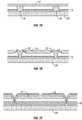
- FIG. 8is a cross section of a display device including an illumination system that includes a light guide panel 80 disposed adjacent a display 81 .
- the light guide panel 80includes a light turning film 89 having light turning features 82 .
- a light source 92injects light into the panel 80 .
- the light turning features 82direct the light propagating through the light guide panel 80 onto the display 81 .
- the light turning features 82are susceptible to light loss, which can reduce the amount of light redirected to the display 81 .
- the features 82are formed by facets 82 a and 82 b , which form angles ⁇ 1 and ⁇ 2 of greater than 90° with surfaces 83 a , 83 b , respectively.
- light incident the facet 82 ais reflected either towards a display 81 or may continue to propagate inside the light guide panel 80 by total internal reflection.
- light incident the facet 82 a at close to the angle of the normal to that surfaceis not reflected and can propagate out of the light guide panel 80 , thereby causing light loss. In display light applications, this light loss can result in reduced display brightness and/or uniformity.
- some embodiments of the inventionprovide slits 100 for redirecting light propagating through a light guide body 180 , which can be a panel of optically transmissive material.
- the slits 100reduce light loss by recycling light that propagates out of the panel 180 .
- the ray 103propagates out of the panel 180 , but is then re-injected into the panel 180 , where it continues to propagate until redirected as desired out of the panel 180 by contact with a facet 104 .
- the slits 100are undercuts in the light guide body 180 and are defined by facets 104 and 106 .
- the volume defined by the “undercut”extends at least partly directly over the surface 108 of the light guide body 180 , when the surface 108 is positioned facing downwards.
- the facet 106 and the surface 108are contiguous through and define an angle 110 , which is less than 90°.
- the slits 100can be filled with another material that facilitates total internal reflection in the body 180 .
- the slits 100can have an open volume and be completely devoid of solid material.
- the facets 104are angled to redirect or reflect, in a desired direction, light propagating through the panel 180 .
- lightis injected into the light guide body by the light source 192 , impinges on the facet 104 and is redirected towards the display 81 .
- the slits 100are lined with an anti-reflective coating 112 in some embodiments.
- the anti-reflective coating 112has advantages for reducing undesired light reflections. For example, for light exiting the facet 104 , the coating 112 can minimize the reflection of light off of the facet 106 , thereby facilitating the re-injection of light into the panel 180 .
- anti-reflective coatingsinclude, without limitation, silicon oxide (SiO 2 ), silicon nitride (SiN 4 ) and aluminum oxide (Al 2 O 3 ) coatings.
- the slits 100form a volume that is open to the surface 108 .
- the slits 100can be disposed completely within the light guide body 180 .
- the slits 100can be formed under the surface 108 and a narrow connecting part 114 at an end of each slit 100 can be sealed, e.g., by the natural resiliency of the material forming the panel 180 , or by application of a sealant or adhesive on those parts.
- the sealing of the parts 114can reduce contamination of or damage to the slits 100 by protecting against external objects that may contact with the surfaces or edges of facets 104 and 106 of the slits 100 .
- the narrow parts 114are not sealed, but the opening defined by that part is relatively narrow compared to the illustrated transverse cross-sectional area of the slits 100 , thereby also providing protection for the slits 100 .
- the illustrated slits 100are not necessarily drawn to scale and their relative sizes can differ. Moreover, the relative angles of the facets 104 and 106 can differ from that illustrated. For example, the cross-sectional areas of the slits 100 can vary and the relative orientations and angles defined by the facets 104 , 106 can vary from slit to slit.
- the facets 104 and 106can be substantially parallel opposite one another, and can be joined by a single slit sidewall 105 that is parallel to the surface 108 .
- the slit 100can thus define a volume having the shape of a parallelogram.
- the parallel orientation of the slit sidewall 105advantageously facilitates total internal reflection of light within the body 102 , since the parallel sidewall 105 reflects light at similar angles to the surface 108 .
- the slits 100can be utilized in various devices in which light turning, or redirection, is desired.
- the slits 100are utilized as light turning features in illumination devices.
- illumination devicescan include wide area lights for indoor or outdoor use.
- illumination devicescan provide overhead lighting for rooms and other indoor spaces.
- FIG. 11Ais a top plan view of a display device having a light guide body 180 and an illumination system including a light bar 190 utilizing the slits 100 as light turning features.
- FIG. 11Bis a cross section of the display device.
- the light bar 190 and light guide body 180are formed of substantially optically transmissive material that can support the propagation of light through the lengths of those structures.
- the light bar 190 and light guide body 180can be formed of glass, plastic or other highly transparent materials.
- the light guide body 180is disposed adjacent and faces a display 181 .
- the slits 100are configured to turn light from the light bar 190 towards the display 181 .
- the illumination systemacts as a front light. Light reflected from the display 181 is transmitted back through and out of the light guide body 180 towards the viewer.
- the display 181can include various display elements, e.g., a plurality of spatial light modulators, interferometric modulators, liquid crystal elements, electrophoretic, etc., which can be arranged parallel the major surface of the panel 180 .
- the display 181is the display 30 ( FIGS. 6A and 6B ) in some embodiments.
- the light bar 190has a first end 190 a for receiving light from a light emitter 192 .
- the light bar 190 and the light emitter 192together form a line light source.
- the light emitter 192may include a light emitting diode (LED), although other light emitting devices are also possible.
- Light emitted from the light emitter 192propagates into the light bar 190 .
- the lightis guided therein, for example, via total internal reflection at sidewalls thereof, which form interfaces with air or some other surrounding fluid or solid medium.
- the light bar 190can be separated from the light guide body 180 by air, fluid or solid medium to promote total internal reflection within the light bar 190 .
- the light bar 190includes slits 100 on at least one side, for example, the side 190 b that is substantially opposite the light guide body 180 .
- the slits 100are configured to turn light incident on that side 190 b of the light bar 190 and to direct that light out of the light bar 190 (e.g., out side 190 c ) into the light guide body 180 .
- the slits 100 shown in FIG. 11Aare schematic. The sizes, shapes, densities, position, etc. of the slits 100 can vary from that depicted to achieve the desired light turning effect.
- the slits 100extend further into the body of the light bar 190 with increasing distance from the side 190 a.
- the illumination apparatusfurther includes a coupling optic (not shown) between the light bar 190 and the light guide body 180 .
- the coupling opticmay collimate, magnify, diffuse, change the color, etc., of light propagating from the light bar 190 .
- lighttravels from the first end 190 a in the direction of a second end 190 d of the light bar 190 , and can be reflected back again towards the first end 190 a .
- the light impinging on the slits 100is turned towards the adjacent light guide body 180 .
- the light guide body 180is disposed with respect to the light bar 190 so as to receive light that has been turned by the slits.
- the light guide body 180redirects light out of the light guide body 180 and towards the display 181 .
- the slits 100are formed along multiple surfaces of the light bar 190 .
- the slits 100are formed along the sides 190 b and 190 c of the light bar 190 . Forming slits 100 on multiple sides can have advantages for more efficiently turning light, per unit length of the light bar 190 .
- the spacing between slits 100 on each side 190 b , 190 ccan be increased for a given density of the slits 100 per unit length of the light bar 190 , which can have advantages for facilitating the manufacturing of dense slit patterns.
- the slits in the surfaces 108 and 109can differ in one or more of total number, transverse cross-sectional shape, dimensions, and angles formed between the slits and the major surfaces.
- a light barsuch as the light bar 190 can be integrated into a light guide body, thereby forming a single light guide body/light bar structure 182 .
- the integrated light guide body/light bar structure 182has advantages for manufacturing and for reducing the number of components in a display device.
- the light turning featurescan take various forms, including prismatic features such as the slits 100 (as discussed further herein), holographic features, or various other light turning features known in the art.
- the light guide body 182 or 180is defined by first and second opposite edges. As illustrated, the slits 100 may be formed in one of these edges and redirect light in a direction towards the opposite edge. Third and fourth edges further define the light guide body 182 , with light entering into the light guide body by impinging, e.g., the third edge (the lower edge in FIG. 11E ).
- the light guide body 182also contains upper and lower major sides or surfaces (stretching from the first to the second edge and from the third to the fourth edge).
- Lightis injected into the light guide body 182 from the light emitter 192 .
- the lightcan be collimated and is redirected by the slits 100 towards the display area 183 , where light turning features redirect the light towards a display (not shown).
- slits 100 closer to the light emitter 192can block light from reaching the surfaces of other slits 100 farther from the light emitter 192 .
- the slits 100extend further along the X-axis, to allow contact with light from the light emitter 192 .
- the slits 100 farthest from the light emitter 192can span substantially the entire length of the emitter 192 along the X-axis.
- the pitch or density of the slits 100 along the Y-axis, the length of the slits 100 along the X-axis and the angles of the slitscan be uniform or can vary to achieve a desired light turning effect.
- the exposed surface area of the slits 100 for contacting and turning lightare substantially equal per unit length along the Y-axis, thereby facilitating a uniform flux of turned light per unit length along the Y-axis.
- light from the light emitter 192is angled towards an edge 184 of the illustrated light guide body 182 , along which the slits 100 are formed.
- the lightcan be angled by, e.g., attaching the light emitter 192 to the light guide body 182 at an angle, or by use of an appropriate optical component or film to direct the light in the desired direction.
- the light that is not turnedcan be recycled, thereby increasing the efficiency of the light extraction relative to arrangements in which the light is not directed along the edge in which the slits 100 are formed.
- additional slits 100are provided in an area 182 corresponding to a display. Light is emitted from the light emitter 192 , the light is then turned by the slits 100 on the edge 184 , and the turned light is turned towards a display (not shown) by the slits 100 in the display area 182 .
- the slits 100can be provided in a light guide body without slits 100 that form the light turning features of a light bar.
- FIG. 12Ashows a cross section of a display device including a light guide body 180 having slits 100 .
- the light bar 190injects light into a first end 180 a of the light guide body 180 .
- the lighttravels from the first end 180 a in the direction of a second end 180 d of the light guide body 180 , and can be reflected back again towards the first end 180 a by total internal reflection.
- some of the lightimpinges on the slits 100 and is turned towards the display 181 .
- the slits 100are formed along the major side or surface 180 b , which faces the display 181 .
- the slits 100can be disposed along both major surfaces of the light guide body 180 , e.g., along both major sides 180 b and 180 c .
- forming slits 100 along multiple surfacescan have advantages for efficiently turning light and for ease of manufacture, where a high density of slits is desired for a unit length of the light guide body 180 . While shown separated from the end 180 a in the FIGS.
- the light bar 190can form an integrated structure with the light guide body 180 , or can be separated.
- the light bar 190 of FIGS. 12A and 12Bcan form a unitary light guide body, with slits in the light bar 190 and a major surface of the light guide body.
- the slits 100can be distributed in the light bar 190 , the light turning light guide body 180 and the integrated light guide body/light bar structure 182 in various patterns to achieved desired light turning properties. It will be appreciated that uniformity of power per area is desired in many applications to uniformly light the display 181 ( FIGS. 11B , 12 A and 12 B). The slits 100 may be arranged to achieve good uniformity in power per area.
- the density of the slits 100increases with increasing distance from the light bar 190 ( FIG. 13A ), the point light emitter 192 ( FIG. 13B ) or the edge 184 ( FIG. 13C ).
- the number of slits 100 per unit areaincreases with increasing distance from the edge of the light guide body 180 directly adjacent the light bar 190 .
- the slits 100extend in substantially straight lights parallel to the light bar 190 .
- the number of slits 100 per unit areaincreases with distance from the point light source 192 .
- the slits 100for semicircular segments centered on the point light source 192 .
- the number of slits 100 per unit areaincreases with distance from the edge 184 .
- the additional slits 100 along that edgeturn light and allow that side of the light guide body 182 to function as a line light source.
- the varying density of the slits 100allows the flux of light redirected per unit area to be highly uniform over the area of the light turning light guide body 180 , 182 corresponding to the display 181 .
- some amount of lightcontacts the slits 100 and is redirected out of the light guide body 180 , 182 .
- the remaining light propagating through the light guide body 180 , 182decreases with distance from the light source, as more and more light is redirected by contact with the slits 100 .
- the density of the slits 100increases with distance from a light point source or line light source.
- the density of the slitsrefers to the area occupied by the slits 100 per unit area of a body of material in which the slits are formed.
- a single large slit 100 or a plurality of smaller slits 100 in a given areamay have the same density.
- the densitymay be changed due to, e.g., changes in the sizes and/or numbers of the slits 100 per area.
- the slits 100can be formed by various methods.
- the slits 100are formed as a body of light propagating material, such as a light guide body or light bar, is formed.
- the body of light propagating materialcan be formed by extrusion through a die having an opening corresponding to a cross-sectional shape of a light guide body or light bar and also having projections in the die corresponding to the slits 100 .
- the material forming the bodyis pushed and/or drawn through the die in the direction in which the slits 100 extend, thereby forming a length of material having the desired cross-sectional shape and having the slits 100 .
- the length of materialis then cut into the desired dimensions for a light guide body or light bar.
- the body of light propagating materialcan be formed by casting, in which material is placed in a mold and allowed to harden.
- the moldcontains extensions corresponding to the slits. Once hardened, the body of light propagating material is removed from the mold.
- the moldcan correspond to a single light guide body or light bar, such that the removed body of light propagating material can be used as a single light turning light guide body or light bar.
- the moldproduces a large sheet of material, which is cut into desired dimensions for one or more light turning light guide bodys and/or light bars.
- the body of light propagating materialis formed by injection molding, in which a fluid material is injected into a mold and then ejected from the mold after hardening.
- the moldcorresponds to a single light guide body or light bar
- the removed body of light propagating materialcan be used as a single light turning light guide body or light bar.
- the moldmay also produce a large sheet of material, and the sheet is cut into desired dimensions for one or more light turning light guide bodys and/or light bars.
- the slits 100are formed after formation of a light turning body.
- the slits 100can be formed by embossing, in which a die, having protrusions corresponding to the slits 100 , is pressed against a body of light propagating material to form the slits 100 in the body.
- the bodycan be heated, making the body sufficiently malleable to take the shape of the slits 100 .
- materialis removed from the body of light propagating material to form the slits 100 .
- the slits 100can be formed by machining or cutting into the body. In other embodiments, material is removed from the body by laser ablation.
- the methods disclosed hereincan be utilized to form light bars and/or light guide bodys.
- the light barscan be formed after formation of the light guide body.
- the sheet of materialcan be cut or stamped into a desired shape. In this cutting or stamping process, slits 100 can be formed at an edge of a light guide body.
- a light guide bodyis formed in sections that are later combined.
- the sectionscan be formed using the methods disclosed herein.
- the sectionsare glued or otherwise attached together with a refractive index matching material to form a single light guide body.
- Section by section formation of a light guide bodyallows the formation of curved slits 100 that may otherwise be difficult for a particular method to form as a single continuous structure.
- the light guide bodyis attached to a display after being formed.
- the light guide bodyis also attached to a light source to form a display device having an illumination system.
Landscapes
- Physics & Mathematics (AREA)
- Engineering & Computer Science (AREA)
- Manufacturing & Machinery (AREA)
- General Physics & Mathematics (AREA)
- Optics & Photonics (AREA)
- Health & Medical Sciences (AREA)
- Ophthalmology & Optometry (AREA)
- Mechanical Engineering (AREA)
- Mechanical Light Control Or Optical Switches (AREA)
Abstract
Description
Claims (28)
Priority Applications (2)
| Application Number | Priority Date | Filing Date | Title |
|---|---|---|---|
| US12/552,124US8358266B2 (en) | 2008-09-02 | 2009-09-01 | Light turning device with prismatic light turning features |
| US13/733,091US20130141938A1 (en) | 2008-09-02 | 2013-01-02 | Light turning device with prismatic light turning features |
Applications Claiming Priority (2)
| Application Number | Priority Date | Filing Date | Title |
|---|---|---|---|
| US9369508P | 2008-09-02 | 2008-09-02 | |
| US12/552,124US8358266B2 (en) | 2008-09-02 | 2009-09-01 | Light turning device with prismatic light turning features |
Related Child Applications (1)
| Application Number | Title | Priority Date | Filing Date |
|---|---|---|---|
| US13/733,091DivisionUS20130141938A1 (en) | 2008-09-02 | 2013-01-02 | Light turning device with prismatic light turning features |
Publications (2)
| Publication Number | Publication Date |
|---|---|
| US20100053148A1 US20100053148A1 (en) | 2010-03-04 |
| US8358266B2true US8358266B2 (en) | 2013-01-22 |
Family
ID=41724666
Family Applications (2)
| Application Number | Title | Priority Date | Filing Date |
|---|---|---|---|
| US12/552,124Expired - Fee RelatedUS8358266B2 (en) | 2008-09-02 | 2009-09-01 | Light turning device with prismatic light turning features |
| US13/733,091AbandonedUS20130141938A1 (en) | 2008-09-02 | 2013-01-02 | Light turning device with prismatic light turning features |
Family Applications After (1)
| Application Number | Title | Priority Date | Filing Date |
|---|---|---|---|
| US13/733,091AbandonedUS20130141938A1 (en) | 2008-09-02 | 2013-01-02 | Light turning device with prismatic light turning features |
Country Status (1)
| Country | Link |
|---|---|
| US (2) | US8358266B2 (en) |
Cited By (9)
| Publication number | Priority date | Publication date | Assignee | Title |
|---|---|---|---|---|
| US20100302616A1 (en)* | 2009-05-29 | 2010-12-02 | Qualcomm Mems Technologies, Inc. | Illumination devices and methods of fabrication thereof |
| US20120163022A1 (en)* | 2009-06-11 | 2012-06-28 | Koninklijke Philips Electronics N.V. | Illumination apparatus |
| US20130188392A1 (en)* | 2009-11-30 | 2013-07-25 | Jun-Bo Yoon | Light guide plate and backlight unit |
| US20180100959A1 (en)* | 2009-04-21 | 2018-04-12 | Sergiy Vasylyev | Illumination system using edge-lit waveguide and microstructured surfaces |
| US10935713B2 (en) | 2017-06-27 | 2021-03-02 | 3M Innovative Properties Company | Unitary lightguide |
| US11199654B2 (en) | 2017-08-08 | 2021-12-14 | 3M Innovative Properties Company | Lightguide having recess of varying depth |
| US11204141B2 (en)* | 2010-12-14 | 2021-12-21 | Bridgelux, Inc. | Side light LED troffer tube |
| US11314008B2 (en) | 2017-08-08 | 2022-04-26 | 3M Innovative Properties Company | Lightguide having opening and surrounding channel |
| CN114600181A (en)* | 2019-10-22 | 2022-06-07 | 镭亚股份有限公司 | Multi-view backlight, multi-view display and method with micro-slit multi-beam elements |
Families Citing this family (59)
| Publication number | Priority date | Publication date | Assignee | Title |
|---|---|---|---|---|
| US20060132383A1 (en)* | 2004-09-27 | 2006-06-22 | Idc, Llc | System and method for illuminating interferometric modulator display |
| US7813026B2 (en)* | 2004-09-27 | 2010-10-12 | Qualcomm Mems Technologies, Inc. | System and method of reducing color shift in a display |
| US7527998B2 (en) | 2006-06-30 | 2009-05-05 | Qualcomm Mems Technologies, Inc. | Method of manufacturing MEMS devices providing air gap control |
| US8107155B2 (en)* | 2006-10-06 | 2012-01-31 | Qualcomm Mems Technologies, Inc. | System and method for reducing visual artifacts in displays |
| US7864395B2 (en) | 2006-10-27 | 2011-01-04 | Qualcomm Mems Technologies, Inc. | Light guide including optical scattering elements and a method of manufacture |
| US7733439B2 (en)* | 2007-04-30 | 2010-06-08 | Qualcomm Mems Technologies, Inc. | Dual film light guide for illuminating displays |
| US8941631B2 (en) | 2007-11-16 | 2015-01-27 | Qualcomm Mems Technologies, Inc. | Simultaneous light collection and illumination on an active display |
| WO2009102731A2 (en) | 2008-02-12 | 2009-08-20 | Qualcomm Mems Technologies, Inc. | Devices and methods for enhancing brightness of displays using angle conversion layers |
| US8654061B2 (en)* | 2008-02-12 | 2014-02-18 | Qualcomm Mems Technologies, Inc. | Integrated front light solution |
| WO2009129264A1 (en)* | 2008-04-15 | 2009-10-22 | Qualcomm Mems Technologies, Inc. | Light with bi-directional propagation |
| CN102047155B (en)* | 2008-05-28 | 2013-04-03 | 高通Mems科技公司 | Light guide panel with light turning microstructure, its manufacturing method and display device |
| US20100051089A1 (en)* | 2008-09-02 | 2010-03-04 | Qualcomm Mems Technologies, Inc. | Light collection device with prismatic light turning features |
| EP2340567A2 (en)* | 2008-09-18 | 2011-07-06 | QUALCOMM MEMS Technologies, Inc. | Increasing the angular range of light collection in solar collectors/concentrators |
| KR20110104090A (en)* | 2009-01-13 | 2011-09-21 | 퀄컴 엠이엠스 테크놀로지스, 인크. | Large Area Light Panels and Screens |
| US8905610B2 (en) | 2009-01-26 | 2014-12-09 | Flex Lighting Ii, Llc | Light emitting device comprising a lightguide film |
| US8270056B2 (en) | 2009-03-23 | 2012-09-18 | Qualcomm Mems Technologies, Inc. | Display device with openings between sub-pixels and method of making same |
| WO2010138762A1 (en)* | 2009-05-29 | 2010-12-02 | Qualcomm Mems Technologies, Inc. | Illumination devices for reflective displays |
| US8270062B2 (en) | 2009-09-17 | 2012-09-18 | Qualcomm Mems Technologies, Inc. | Display device with at least one movable stop element |
| US8488228B2 (en)* | 2009-09-28 | 2013-07-16 | Qualcomm Mems Technologies, Inc. | Interferometric display with interferometric reflector |
| US20110169428A1 (en)* | 2010-01-08 | 2011-07-14 | Qualcomm Mems Technologies, Inc. | Edge bar designs to mitigate edge shadow artifact |
| US20110169724A1 (en)* | 2010-01-08 | 2011-07-14 | Qualcomm Mems Technologies, Inc. | Interferometric pixel with patterned mechanical layer |
| KR20130100232A (en) | 2010-04-09 | 2013-09-10 | 퀄컴 엠이엠에스 테크놀로지스, 인크. | Mechanical layer of an electromechanical device and methods of forming the same |
| US9651729B2 (en) | 2010-04-16 | 2017-05-16 | Flex Lighting Ii, Llc | Reflective display comprising a frontlight with extraction features and a light redirecting optical element |
| CN103109315A (en) | 2010-08-17 | 2013-05-15 | 高通Mems科技公司 | Actuation and calibration of a charge neutral electrode in an interferometric display device |
| US8402647B2 (en) | 2010-08-25 | 2013-03-26 | Qualcomm Mems Technologies Inc. | Methods of manufacturing illumination systems |
| US9057872B2 (en) | 2010-08-31 | 2015-06-16 | Qualcomm Mems Technologies, Inc. | Dielectric enhanced mirror for IMOD display |
| US8902484B2 (en) | 2010-12-15 | 2014-12-02 | Qualcomm Mems Technologies, Inc. | Holographic brightness enhancement film |
| CA2829388C (en)* | 2011-03-09 | 2018-09-25 | Flex Lighting Ii, Llc | Light emitting device with adjustable light output profile |
| US8963159B2 (en) | 2011-04-04 | 2015-02-24 | Qualcomm Mems Technologies, Inc. | Pixel via and methods of forming the same |
| US9134527B2 (en) | 2011-04-04 | 2015-09-15 | Qualcomm Mems Technologies, Inc. | Pixel via and methods of forming the same |
| US8659816B2 (en) | 2011-04-25 | 2014-02-25 | Qualcomm Mems Technologies, Inc. | Mechanical layer and methods of making the same |
| US8736939B2 (en) | 2011-11-04 | 2014-05-27 | Qualcomm Mems Technologies, Inc. | Matching layer thin-films for an electromechanical systems reflective display device |
| US11009646B2 (en) | 2013-03-12 | 2021-05-18 | Azumo, Inc. | Film-based lightguide with interior light directing edges in a light mixing region |
| IL235642B (en) | 2014-11-11 | 2021-08-31 | Lumus Ltd | Compact head-mounted display system protected by a hyperfine structure |
| IL237337B (en) | 2015-02-19 | 2020-03-31 | Amitai Yaakov | Compact head-mounted display system having uniform image |
| WO2018065975A1 (en) | 2016-10-09 | 2018-04-12 | Lumus Ltd | Aperture multiplier using a rectangular waveguide |
| KR20240160657A (en) | 2016-11-08 | 2024-11-11 | 루머스 리미티드 | Light-guide device with optical cutoff edge and corresponding production methods |
| CN108738358B (en) | 2017-02-22 | 2021-03-26 | 鲁姆斯有限公司 | Light guide optics |
| CN109416433B (en)* | 2017-03-22 | 2021-06-01 | 鲁姆斯有限公司 | Overlapping Reflector Construction |
| EP4215980A1 (en) | 2017-07-19 | 2023-07-26 | Lumus Ltd. | Lcos illumination via loe |
| IL259518B2 (en) | 2018-05-22 | 2023-04-01 | Lumus Ltd | Optical system and method for improvement of light field uniformity |
| MX2020012512A (en) | 2018-05-23 | 2021-02-16 | Lumus Ltd | Optical system including light-guide optical element with partially-reflective internal surfaces. |
| US11415812B2 (en) | 2018-06-26 | 2022-08-16 | Lumus Ltd. | Compact collimating optical device and system |
| WO2020047340A1 (en) | 2018-08-30 | 2020-03-05 | Flex Lighting Ii, Llc | Film-based frontlight with angularly varying diffusion film |
| EP3894917A4 (en) | 2018-12-11 | 2022-07-13 | Azumo, Inc. | FRONT LIGHTING LIGHT GUIDE WITH DIFFUSE REFLECTIVE SEPARATOR |
| WO2020142731A1 (en) | 2019-01-03 | 2020-07-09 | Flex Lighting Ii, Llc | Reflective display comprising a lightguide and light turning film creating multiple illumination peaks |
| CN113678036B (en) | 2019-01-09 | 2024-02-02 | 阿祖莫公司 | Reflective display including coupled light guides folded at different folding angles |
| WO2020174433A1 (en) | 2019-02-28 | 2020-09-03 | Lumus Ltd. | Compact collimated image projector |
| TWI800657B (en) | 2019-03-12 | 2023-05-01 | 以色列商魯姆斯有限公司 | Image projector |
| EP3956604A4 (en) | 2019-04-15 | 2022-06-08 | Lumus Ltd. | PROCESS FOR MANUFACTURING AN OPTICAL LIGHT GUIDE ELEMENT |
| AU2020300121B2 (en) | 2019-07-04 | 2024-06-13 | Lumus Ltd. | Image waveguide with symmetric beam multiplication |
| WO2021022307A1 (en) | 2019-08-01 | 2021-02-04 | Flex Lighting Ii, Llc | Lightguide with a light input edge between lateral edges of a folded strip |
| TWI884834B (en)* | 2019-12-05 | 2025-05-21 | 以色列商魯姆斯有限公司 | Optical device and method of fabricating optical device |
| US11523092B2 (en) | 2019-12-08 | 2022-12-06 | Lumus Ltd. | Optical systems with compact image projector |
| CN218848473U (en) | 2020-05-12 | 2023-04-11 | 鲁姆斯有限公司 | Equipment including projection optics and light guides |
| CN115176190B (en) | 2020-05-24 | 2024-07-09 | 鲁姆斯有限公司 | Composite light guide optical element |
| WO2022044006A1 (en) | 2020-08-26 | 2022-03-03 | Lumus Ltd. | Generation of color images using white light as source |
| TW202300988A (en) | 2021-05-19 | 2023-01-01 | 以色列商魯姆斯有限公司 | Active optical engine |
| WO2024038458A1 (en) | 2022-08-18 | 2024-02-22 | Lumus Ltd. | Image projector with polarizing catadioptric collimator |
Citations (457)
| Publication number | Priority date | Publication date | Assignee | Title |
|---|---|---|---|---|
| US2590906A (en) | 1946-11-22 | 1952-04-01 | Farrand Optical Co Inc | Reflection interference filter |
| US2677714A (en) | 1951-09-21 | 1954-05-04 | Alois Vogt Dr | Optical-electrical conversion device comprising a light-permeable metal electrode |
| US3247392A (en) | 1961-05-17 | 1966-04-19 | Optical Coating Laboratory Inc | Optical coating and assembly used as a band pass interference filter reflecting in the ultraviolet and infrared |
| US3679313A (en) | 1970-10-23 | 1972-07-25 | Bell Telephone Labor Inc | Dispersive element for optical pulse compression |
| US3728030A (en) | 1970-06-22 | 1973-04-17 | Cary Instruments | Polarization interferometer |
| US3886310A (en) | 1973-08-22 | 1975-05-27 | Westinghouse Electric Corp | Electrostatically deflectable light valve with improved diffraction properties |
| US3955190A (en) | 1972-09-11 | 1976-05-04 | Kabushiki Kaisha Suwa Seikosha | Electro-optical digital display |
| US4154219A (en) | 1977-03-11 | 1979-05-15 | E-Systems, Inc. | Prismatic solar reflector apparatus and method of solar tracking |
| US4282862A (en) | 1979-11-09 | 1981-08-11 | Soleau Bertrand S | Thin-line collectors |
| US4375312A (en) | 1980-08-07 | 1983-03-01 | Hughes Aircraft Company | Graded index waveguide structure and process for forming same |
| US4403248A (en) | 1980-03-04 | 1983-09-06 | U.S. Philips Corporation | Display device with deformable reflective medium |
| US4421381A (en) | 1980-04-04 | 1983-12-20 | Yokogawa Hokushin Electric Corp. | Mechanical vibrating element |
| US4441789A (en) | 1980-03-31 | 1984-04-10 | Jenoptik Jena Gmbh | Resonance absorber |
| US4441791A (en) | 1980-09-02 | 1984-04-10 | Texas Instruments Incorporated | Deformable mirror light modulator |
| US4497974A (en) | 1982-11-22 | 1985-02-05 | Exxon Research & Engineering Co. | Realization of a thin film solar cell with a detached reflector |
| US4498953A (en) | 1983-07-27 | 1985-02-12 | At&T Bell Laboratories | Etching techniques |
| US4560435A (en) | 1984-10-01 | 1985-12-24 | International Business Machines Corporation | Composite back-etch/lift-off stencil for proximity effect minimization |
| US4655554A (en) | 1985-03-06 | 1987-04-07 | The United States Of America As Represented By The Secretary Of The Air Force | Spatial light modulator having a capacitively coupled photoconductor |
| US4705361A (en) | 1985-11-27 | 1987-11-10 | Texas Instruments Incorporated | Spatial light modulator |
| EP0278038A1 (en) | 1987-02-13 | 1988-08-17 | Battelle-Institut e.V. | Active flat type display panel |
| US4779959A (en) | 1986-09-05 | 1988-10-25 | The Secretary Of State For Defence In Her Britannic Majesty's Government Of The United Kingdom Of Great Britain And Northern Ireland | Liquid crystal electro-optic modulator in a fabry-perot interferometer |
| US4786128A (en) | 1986-12-02 | 1988-11-22 | Quantum Diagnostics, Ltd. | Device for modulating and reflecting electromagnetic radiation employing electro-optic layer having a variable index of refraction |
| US4822993A (en) | 1987-02-17 | 1989-04-18 | Optron Systems, Inc. | Low-cost, substantially cross-talk free high spatial resolution 2-D bistable light modulator |
| US4859060A (en) | 1985-11-26 | 1989-08-22 | 501 Sharp Kabushiki Kaisha | Variable interferometric device and a process for the production of the same |
| US4925259A (en) | 1988-10-20 | 1990-05-15 | The United States Of America As Represented By The United States Department Of Energy | Multilayer optical dielectric coating |
| US4954789A (en) | 1989-09-28 | 1990-09-04 | Texas Instruments Incorporated | Spatial light modulator |
| US4956619A (en) | 1988-02-19 | 1990-09-11 | Texas Instruments Incorporated | Spatial light modulator |
| US4973131A (en) | 1989-02-03 | 1990-11-27 | Mcdonnell Douglas Corporation | Modulator mirror |
| US4982184A (en) | 1989-01-03 | 1991-01-01 | General Electric Company | Electrocrystallochromic display and element |
| US5022745A (en) | 1989-09-07 | 1991-06-11 | Massachusetts Institute Of Technology | Electrostatically deformable single crystal dielectrically coated mirror |
| US5028939A (en) | 1988-08-23 | 1991-07-02 | Texas Instruments Incorporated | Spatial light modulator system |
| US5062689A (en) | 1990-08-21 | 1991-11-05 | Koehler Dale R | Electrostatically actuatable light modulating device |
| US5091983A (en) | 1987-06-04 | 1992-02-25 | Walter Lukosz | Optical modulation apparatus and measurement method |
| US5096279A (en) | 1984-08-31 | 1992-03-17 | Texas Instruments Incorporated | Spatial light modulator and method |
| US5123247A (en) | 1990-02-14 | 1992-06-23 | 116736 (Canada) Inc. | Solar roof collector |
| US5170283A (en) | 1991-07-24 | 1992-12-08 | Northrop Corporation | Silicon spatial light modulator |
| US5206747A (en) | 1988-09-28 | 1993-04-27 | Taliq Corporation | Polymer dispersed liquid crystal display with birefringence of the liquid crystal at least 0.23 |
| EP0539099A3 (en) | 1991-10-25 | 1993-05-19 | Optical Coating Laboratory, Inc. | Repositionable optical cover for monitors |
| US5291314A (en) | 1990-07-27 | 1994-03-01 | France Telecom | Spatial light modulator device and a conoscopic holography system of large dynamic range including such a modulator device |
| EP0590511A1 (en) | 1992-10-01 | 1994-04-06 | International Business Machines Corporation | Edge-lit transflective non-emissive display |
| US5315370A (en) | 1991-10-23 | 1994-05-24 | Bulow Jeffrey A | Interferometric modulator for optical signal processing |
| EP0621500A1 (en) | 1993-04-23 | 1994-10-26 | AT&T Corp. | Illuminated transparent display with microtextured back reflector |
| US5381232A (en) | 1992-05-19 | 1995-01-10 | Akzo Nobel N.V. | Fabry-perot with device mirrors including a dielectric coating outside the resonant cavity |
| US5452138A (en) | 1991-07-31 | 1995-09-19 | Texas Instruments Incorporated | Deformable mirror device with integral color filter |
| US5471341A (en) | 1991-07-17 | 1995-11-28 | Optron Systems, Inc. | Membrane light modulating systems |
| EP0695959A1 (en) | 1994-07-29 | 1996-02-07 | AT&T Corp. | Direct view display based on a micromechanical modulator |
| US5526172A (en) | 1993-07-27 | 1996-06-11 | Texas Instruments Incorporated | Microminiature, monolithic, variable electrical signal processor and apparatus including same |
| US5550373A (en) | 1994-12-30 | 1996-08-27 | Honeywell Inc. | Fabry-Perot micro filter-detector |
| US5555160A (en) | 1991-06-27 | 1996-09-10 | Nissen Chemitec Co., Ltd. | Light-guiding panel for surface lighting and a surface lighting body |
| US5559358A (en) | 1993-05-25 | 1996-09-24 | Honeywell Inc. | Opto-electro-mechanical device or filter, process for making, and sensors made therefrom |
| US5561523A (en) | 1994-02-17 | 1996-10-01 | Vaisala Oy | Electrically tunable fabry-perot interferometer produced by surface micromechanical techniques for use in optical material analysis |
| US5592332A (en) | 1992-12-25 | 1997-01-07 | Dai Nippon Printing Co., Ltd. | Renticular lens, surface light source, and liquid crystal display apparatus |
| US5597736A (en) | 1992-08-11 | 1997-01-28 | Texas Instruments Incorporated | High-yield spatial light modulator with light blocking layer |
| US5600383A (en) | 1990-06-29 | 1997-02-04 | Texas Instruments Incorporated | Multi-level deformable mirror device with torsion hinges placed in a layer different from the torsion beam layer |
| US5646768A (en) | 1994-07-29 | 1997-07-08 | Texas Instruments Incorporated | Support posts for micro-mechanical devices |
| US5646729A (en) | 1993-01-13 | 1997-07-08 | Vaisala Oy | Single-channel gas concentration measurement method and apparatus using a short-resonator Fabry-Perot interferometer |
| US5661592A (en) | 1995-06-07 | 1997-08-26 | Silicon Light Machines | Method of making and an apparatus for a flat diffraction grating light valve |
| US5665997A (en) | 1994-03-31 | 1997-09-09 | Texas Instruments Incorporated | Grated landing area to eliminate sticking of micro-mechanical devices |
| US5671994A (en) | 1994-06-08 | 1997-09-30 | Clio Technologies, Inc. | Flat and transparent front-lighting system using microprisms |
| US5699181A (en) | 1995-07-27 | 1997-12-16 | Samsung Electronics Co., Ltd. | Deformable mirror device and manufacturing method thereof |
| US5710656A (en) | 1996-07-30 | 1998-01-20 | Lucent Technologies Inc. | Micromechanical optical modulator having a reduced-mass composite membrane |
| US5712694A (en) | 1994-09-16 | 1998-01-27 | Kabushiki Kaisha Toshiba | LCD comprising a light separating element including a cholesteric liquid crystal sheet |
| US5719068A (en) | 1994-11-25 | 1998-02-17 | Semiconductor Energy Laboratory Co., Ltd. | Method for anisotropic etching conductive film |
| US5734177A (en) | 1995-10-31 | 1998-03-31 | Sharp Kabushiki Kaisha | Semiconductor device, active-matrix substrate and method for fabricating the same |
| US5771116A (en) | 1996-10-21 | 1998-06-23 | Texas Instruments Incorporated | Multiple bias level reset waveform for enhanced DMD control |
| US5783614A (en) | 1997-02-21 | 1998-07-21 | Copytele, Inc. | Polymeric-coated dielectric particles and formulation and method for preparing same |
| US5786927A (en) | 1997-03-12 | 1998-07-28 | Lucent Technologies Inc. | Gas-damped micromechanical structure |
| US5808781A (en) | 1996-02-01 | 1998-09-15 | Lucent Technologies Inc. | Method and apparatus for an improved micromechanical modulator |
| US5825528A (en) | 1995-12-26 | 1998-10-20 | Lucent Technologies Inc. | Phase-mismatched fabry-perot cavity micromechanical modulator |
| US5838484A (en) | 1996-08-19 | 1998-11-17 | Lucent Technologies Inc. | Micromechanical optical modulator with linear operating characteristic |
| EP0879991A2 (en) | 1997-05-13 | 1998-11-25 | Matsushita Electric Industrial Co., Ltd. | Illuminating system |
| US5867302A (en) | 1997-08-07 | 1999-02-02 | Sandia Corporation | Bistable microelectromechanical actuator |
| US5870221A (en) | 1997-07-25 | 1999-02-09 | Lucent Technologies, Inc. | Micromechanical modulator having enhanced performance |
| GB2331615A (en) | 1997-11-21 | 1999-05-26 | Mitsubishi Electric Corp | A backlight for a liquid crystal display |
| US5914804A (en) | 1998-01-28 | 1999-06-22 | Lucent Technologies Inc | Double-cavity micromechanical optical modulator with plural multilayer mirrors |
| US5920418A (en) | 1994-06-21 | 1999-07-06 | Matsushita Electric Industrial Co., Ltd. | Diffractive optical modulator and method for producing the same, infrared sensor including such a diffractive optical modulator and method for producing the same, and display device including such a diffractive optical modulator |
| US5961848A (en) | 1994-11-10 | 1999-10-05 | Thomson-Csf | Process for producing magnetoresistive transducers |
| US5961198A (en) | 1996-02-02 | 1999-10-05 | Hitachi, Ltd. | Liquid crystal display device and method of manufacturing backlighting light guide panel therefor |
| US6021007A (en) | 1997-10-18 | 2000-02-01 | Murtha; R. Michael | Side-collecting lightguide |
| US6028689A (en) | 1997-01-24 | 2000-02-22 | The United States Of America As Represented By The Secretary Of The Air Force | Multi-motion micromirror |
| US6031653A (en) | 1997-08-28 | 2000-02-29 | California Institute Of Technology | Low-cost thin-metal-film interference filters |
| JP2000075293A (en) | 1998-09-02 | 2000-03-14 | Matsushita Electric Ind Co Ltd | Illumination device, illuminated touch panel and reflective liquid crystal display device |
| EP0986077A2 (en) | 1998-09-12 | 2000-03-15 | Lucent Technologies Inc. | Article comprising a multi-port variable capacitor |
| US6040937A (en) | 1994-05-05 | 2000-03-21 | Etalon, Inc. | Interferometric modulation |
| US6046659A (en) | 1998-05-15 | 2000-04-04 | Hughes Electronics Corporation | Design and fabrication of broadband surface-micromachined micro-electro-mechanical switches for microwave and millimeter-wave applications |
| JP2000147262A (en) | 1998-11-11 | 2000-05-26 | Nobuyuki Higuchi | Converging device and photovoltaic power generation system utilizing the device |
| JP2000193933A (en) | 1998-12-25 | 2000-07-14 | Matsushita Electric Works Ltd | Display device |
| US6100861A (en) | 1998-02-17 | 2000-08-08 | Rainbow Displays, Inc. | Tiled flat panel display with improved color gamut |
| US6123431A (en) | 1997-03-19 | 2000-09-26 | Sanyo Electric Co., Ltd | Backlight apparatus and light guide plate |
| US6124851A (en) | 1995-07-20 | 2000-09-26 | E Ink Corporation | Electronic book with multiple page displays |
| JP2000314882A (en) | 1999-04-30 | 2000-11-14 | Hitachi Ltd | Liquid crystal display device, light guide plate and method of manufacturing light guide plate |
| US6195196B1 (en) | 1998-03-13 | 2001-02-27 | Fuji Photo Film Co., Ltd. | Array-type exposing device and flat type display incorporating light modulator and driving method thereof |
| US6242932B1 (en) | 1999-02-19 | 2001-06-05 | Micron Technology, Inc. | Interposer for semiconductor components having contact balls |
| US20010003487A1 (en) | 1996-11-05 | 2001-06-14 | Mark W. Miles | Visible spectrum modulator arrays |
| US6259854B1 (en) | 1997-05-29 | 2001-07-10 | Kuraray Co., Ltd. | Lightguide |
| US6262697B1 (en) | 1998-03-20 | 2001-07-17 | Eastman Kodak Company | Display having viewable and conductive images |
| GB2351834B (en) | 1999-07-06 | 2001-08-15 | Nec Corp | Liquid-Crystal display and electronic device incorporating the display |
| JP2001221913A (en) | 2000-02-08 | 2001-08-17 | Yokogawa Electric Corp | Fabry-Perot filter and infrared gas analyzer |
| JP2001249283A (en) | 2000-02-22 | 2001-09-14 | Marconi Communications Ltd | Wavelength selective optical filter |
| US6292504B1 (en) | 1999-03-16 | 2001-09-18 | Raytheon Company | Dual cavity laser resonator |
| US6301000B1 (en) | 1999-01-11 | 2001-10-09 | Kenneth Carlisle Johnson | Dual-flexure light valve |
| US20010028503A1 (en) | 2000-03-03 | 2001-10-11 | Flanders Dale C. | Integrated tunable fabry-perot filter and method of making same |
| US20010043171A1 (en) | 2000-02-24 | 2001-11-22 | Van Gorkom Gerardus Gegorius Petrus | Display device comprising a light guide |
| US6323987B1 (en) | 1999-05-14 | 2001-11-27 | Agere Systems Optoelectronics Guardian Corp. | Controlled multi-wavelength etalon |
| US6327071B1 (en) | 1998-10-16 | 2001-12-04 | Fuji Photo Film Co., Ltd. | Drive methods of array-type light modulation element and flat-panel display |
| US20010055208A1 (en) | 2000-06-15 | 2001-12-27 | Koichi Kimura | Optical element, optical light source unit and optical display device equipped with the optical light source unit |
| US6335235B1 (en) | 1999-08-17 | 2002-01-01 | Advanced Micro Devices, Inc. | Simplified method of patterning field dielectric regions in a semiconductor device |
| US6351329B1 (en) | 1999-10-08 | 2002-02-26 | Lucent Technologies Inc. | Optical attenuator |
| JP2002062490A (en) | 2000-08-14 | 2002-02-28 | Canon Inc | Interferometric modulator |
| US6356378B1 (en) | 1995-06-19 | 2002-03-12 | Reflectivity, Inc. | Double substrate reflective spatial light modulator |
| JP2002108227A (en) | 2000-07-26 | 2002-04-10 | Bridgestone Corp | Front light and liquid crystal display device |
| US6377233B2 (en) | 1998-10-08 | 2002-04-23 | International Business Machines Corporation | Micromechanical display and fabrication method |
| US6381022B1 (en) | 1992-01-22 | 2002-04-30 | Northeastern University | Light modulating device |
| US6384952B1 (en) | 1997-03-27 | 2002-05-07 | Mems Optical Inc. | Vertical comb drive actuated deformable mirror device and method |
| US20020054424A1 (en) | 1994-05-05 | 2002-05-09 | Etalon, Inc. | Photonic mems and structures |
| EP1205782A3 (en) | 2000-11-01 | 2002-05-29 | Agilent Technologies, Inc. (a Delaware corporation) | Optically tunable Fabry-Perot micro-electromechanical resonator |
| US6400738B1 (en) | 2000-04-14 | 2002-06-04 | Agilent Technologies, Inc. | Tunable Fabry-Perot filters and lasers |
| US20020070931A1 (en) | 2000-07-03 | 2002-06-13 | Hiroichi Ishikawa | Optical multilayer structure, optical switching device, and image display |
| US6407785B1 (en) | 1998-10-05 | 2002-06-18 | Semiconductor Energy Laboratory Co., Ltd. | Reflection type semiconductor display device having optical fiber adjacent the surface of the main body |
| US20020075555A1 (en) | 1994-05-05 | 2002-06-20 | Iridigm Display Corporation | Interferometric modulation of radiation |
| JP2002174780A (en) | 2000-12-08 | 2002-06-21 | Stanley Electric Co Ltd | Reflective color display |
| US20020080465A1 (en) | 2000-11-03 | 2002-06-27 | Intpax, Inc. | MEMS based variable optical attenuator (MBVOA) |
| US20020106182A1 (en) | 2001-02-02 | 2002-08-08 | Minebea Co., Ltd. | Spread illuminating apparatus with cover provided over transparent substrate |
| JP2002221678A (en) | 2001-01-25 | 2002-08-09 | Seiko Epson Corp | Optical switching device, manufacturing method thereof, and image display device |
| US6433917B1 (en) | 2000-11-22 | 2002-08-13 | Ball Semiconductor, Inc. | Light modulation device and system |
| JP2002229023A (en) | 2001-02-05 | 2002-08-14 | Rohm Co Ltd | Color liquid crystal display device |
| US6437583B1 (en) | 1996-02-14 | 2002-08-20 | Stmicroelectronics, Inc.. | Capacitive distance sensor |
| US6438282B1 (en) | 1998-01-20 | 2002-08-20 | Seiko Epson Corporation | Optical switching device and image display device |
| US20020113241A1 (en) | 2000-07-24 | 2002-08-22 | Tdk Corporation | Light emitting device |
| JP2002245835A (en) | 2001-02-15 | 2002-08-30 | Minolta Co Ltd | Illumination device, display device, and electronic equipment |
| US6452712B2 (en) | 1995-12-01 | 2002-09-17 | Seiko Epson Corporation | Method of manufacturing spatial light modulator and electronic device employing it |
| US20020146200A1 (en) | 2001-03-16 | 2002-10-10 | Kudrle Thomas David | Electrostatically actuated micro-electro-mechanical devices and method of manufacture |
| US6466354B1 (en) | 2000-09-19 | 2002-10-15 | Silicon Light Machines | Method and apparatus for interferometric modulation of light |
| US20020149834A1 (en) | 2000-12-22 | 2002-10-17 | Ball Semiconductor, Inc. | Light modulation device and system |
| US20020149828A1 (en) | 1994-05-05 | 2002-10-17 | Miles Mark W. | Controlling micro-electro-mechanical cavities |
| US20020154422A1 (en) | 2001-04-23 | 2002-10-24 | Sniegowski Jeffry J. | Surface micromachined optical system with reinforced mirror microstructure |
| US20020197761A1 (en) | 2001-05-22 | 2002-12-26 | Reflectivity, Inc. | Method for making a micromechanical device by removing a sacrificial layer with multiple sequential etchants |
| EP1271223A2 (en) | 2001-06-28 | 2003-01-02 | Nokia Corporation | Electronic display |
| EP1227346A3 (en) | 1996-09-23 | 2003-01-08 | Qinetiq Limited | Multi layer interference coatings |
| US20030011864A1 (en) | 2001-07-16 | 2003-01-16 | Axsun Technologies, Inc. | Tilt mirror fabry-perot filter system, fabrication process therefor, and method of operation thereof |
| US20030016428A1 (en) | 2001-07-11 | 2003-01-23 | Takahisa Kato | Light deflector, method of manufacturing light deflector, optical device using light deflector, and torsion oscillating member |
| US6512626B1 (en) | 1999-06-16 | 2003-01-28 | Creavis Gesellschaft Fuer Technologie Und Innovation Mbh | Composite sheets with electrically switchable optical properties made of light-scattering base material |
| US20030026536A1 (en) | 2001-08-02 | 2003-02-06 | Edward Ho | Apparatus and method for collecting light |
| US6519073B1 (en) | 2000-01-10 | 2003-02-11 | Lucent Technologies Inc. | Micromechanical modulator and methods for fabricating the same |
| US20030030764A1 (en) | 2001-07-13 | 2003-02-13 | Hea-Chun Lee | Light guiding plate, method of manufacturing the same and liquid crystal display having the light guiding plate |
| US20030034445A1 (en) | 2001-08-15 | 2003-02-20 | Boyd Gary T. | Light guide for use with backlit display |
| US20030035196A1 (en) | 2001-08-17 | 2003-02-20 | Walker James A. | Optical modulator and method of manufacture thereof |
| JP2003057653A (en) | 2001-08-21 | 2003-02-26 | Citizen Watch Co Ltd | Liquid crystal display device |
| US20030043157A1 (en) | 1999-10-05 | 2003-03-06 | Iridigm Display Corporation | Photonic MEMS and structures |
| US20030053078A1 (en) | 2001-09-17 | 2003-03-20 | Mark Missey | Microelectromechanical tunable fabry-perot wavelength monitor with thermal actuators |
| US20030071947A1 (en) | 2001-07-05 | 2003-04-17 | Miki Shiraogawa | Optical film and a liquid crystal display using the same |
| US20030083429A1 (en) | 1995-09-28 | 2003-05-01 | Alliedsignal Inc. | Colored articles and compositions and methods for their fabrication |
| US20030086031A1 (en) | 2000-06-29 | 2003-05-08 | Hitoshi Taniguchi | Liquid crystal display device |
| US20030086030A1 (en) | 2001-11-08 | 2003-05-08 | Hitoshi Taniguchi | Backlit lighting device, liquid crystal display device utilizing same, and liquid crystal display device manufacturing method |
| US20030090887A1 (en) | 2001-11-12 | 2003-05-15 | Nidec Copal Corporation | Light-guide plate and method for manufacturing the same |
| US20030095401A1 (en) | 2001-11-20 | 2003-05-22 | Palm, Inc. | Non-visible light display illumination system and method |
| US6574033B1 (en) | 2002-02-27 | 2003-06-03 | Iridigm Display Corporation | Microelectromechanical systems device and method for fabricating same |
| US20030103344A1 (en) | 2001-11-30 | 2003-06-05 | Eiki Niida | Wedge plate type light guiding plate for front light |
| US20030119221A1 (en) | 2001-11-09 | 2003-06-26 | Coventor, Inc. | Trilayered beam MEMS device and related methods |
| JP2003177336A (en) | 2001-12-11 | 2003-06-27 | Fuji Photo Film Co Ltd | Optical modulating element, optical modulating element array, and exposure device using the same |
| US20030123245A1 (en) | 1995-06-27 | 2003-07-03 | Parker Jeffery R. | Light emitting panel assemblies |
| US20030123125A1 (en) | 2000-03-20 | 2003-07-03 | Np Photonics, Inc. | Detunable Fabry-Perot interferometer and an add/drop multiplexer using the same |
| US20030128538A1 (en) | 2000-02-28 | 2003-07-10 | Masayuki Shinohara | Surface light source, method for manufacturing the same and apparatus using it |
| US6592234B2 (en) | 2001-04-06 | 2003-07-15 | 3M Innovative Properties Company | Frontlit display |
| US6597490B2 (en) | 1995-09-29 | 2003-07-22 | Coretek, Inc. | Electrically tunable fabry-perot structure utilizing a deformable multi-layer mirror and method of making the same |
| US20030138669A1 (en) | 2001-12-07 | 2003-07-24 | Rie Kojima | Information recording medium and method for producing the same |
| US6601984B2 (en)* | 2001-02-14 | 2003-08-05 | Estec Co., Ltd. | LED illuminating device and lighting apparatus employing the same |
| US6608268B1 (en) | 2002-02-05 | 2003-08-19 | Memtronics, A Division Of Cogent Solutions, Inc. | Proximity micro-electro-mechanical system |
| US20030165067A1 (en) | 2001-12-04 | 2003-09-04 | Norihiro Imamura | Liquid crystal display and lighting unit used for the same |
| US20030169385A1 (en) | 2002-03-05 | 2003-09-11 | Citizen Electronics Co., Ltd. | Illumination device for a color liquid crystal display |
| EP1251454A3 (en) | 2001-04-16 | 2003-09-17 | Nitto Denko Corporation | Touch panel including illuminator and reflective liquid-crystal display device |
| US20030173504A1 (en) | 2002-03-18 | 2003-09-18 | Honeywell International Inc. | Spectrally tunable detector |
| US20030184989A1 (en) | 2002-03-29 | 2003-10-02 | Citizen Watch Co., Ltd. & Citizen Electronics Co., Ltd. | Lighting device for lighting a liquid crystal display |
| US6632698B2 (en) | 2001-08-07 | 2003-10-14 | Hewlett-Packard Development Company, L.P. | Microelectromechanical device having a stiffened support beam, and methods of forming stiffened support beams in MEMS |
| US20030202266A1 (en) | 2002-04-30 | 2003-10-30 | Ring James W. | Micro-mirror device with light angle amplification |
| US20030202265A1 (en) | 2002-04-30 | 2003-10-30 | Reboa Paul F. | Micro-mirror device including dielectrophoretic liquid |
| US20030210222A1 (en) | 2000-07-31 | 2003-11-13 | Akifumi Ogiwara | Illuminator, image display, liquid crystal monitor, liquid crystal television, liquid crystal information terminal, and method for producing light guide plate |
| US20030210367A1 (en) | 2002-05-07 | 2003-11-13 | Nitto Denko Corporation | Reflection-type liquid-crystal display, and optical film |
| US6657832B2 (en) | 2001-04-26 | 2003-12-02 | Texas Instruments Incorporated | Mechanically assisted restoring force support for micromachined membranes |
| JP2003340795A (en) | 2002-05-20 | 2003-12-02 | Sony Corp | Electrostatic drive type mems element and manufacturing method therefor, optical mems element, optical modulator, glv device and laser display |
| US6657683B2 (en) | 1999-10-22 | 2003-12-02 | Motorola, Inc. | Front illuminator for a liquid crystal display and method of making same |
| JP2003344881A (en) | 2002-05-22 | 2003-12-03 | Alps Electric Co Ltd | Electrophoretic display |
| US6661561B2 (en) | 2001-03-26 | 2003-12-09 | Creo Inc. | High frequency deformable mirror device |
| TW567388B (en) | 2001-06-16 | 2003-12-21 | Che-Chih Tsao | Pattern projection techniques for volumetric 3D displays and 2D displays |
| US6667782B1 (en) | 1999-10-08 | 2003-12-23 | International Business Machines Corporation | Light guide apparatus, a backlight apparatus and a liquid crystal display apparatus |
| US6669350B2 (en) | 2000-12-14 | 2003-12-30 | Mitsubish Rayon Co., Ltd. | Planar light source system and light deflecting device therefor |
| US20040001169A1 (en) | 2002-02-12 | 2004-01-01 | Yuuji Saiki | Polarizer, polarizing plate, liquid crystal display, and image display, and a method for producing the polarizer |
| US6674562B1 (en) | 1994-05-05 | 2004-01-06 | Iridigm Display Corporation | Interferometric modulation of radiation |
| US20040008396A1 (en) | 2002-01-09 | 2004-01-15 | The Regents Of The University Of California | Differentially-driven MEMS spatial light modulator |
| US20040008438A1 (en) | 2002-06-04 | 2004-01-15 | Nec Corporation | Tunable filter, manufacturing method thereof and optical switching device comprising the tunable filter |
| US20040027701A1 (en) | 2001-07-12 | 2004-02-12 | Hiroichi Ishikawa | Optical multilayer structure and its production method, optical switching device, and image display |
| US20040027671A1 (en) | 2002-08-09 | 2004-02-12 | Xingtao Wu | Tunable optical filter |
| US6698295B1 (en) | 2000-03-31 | 2004-03-02 | Shipley Company, L.L.C. | Microstructures comprising silicon nitride layer and thin conductive polysilicon layer |
| US20040043552A1 (en) | 2000-12-15 | 2004-03-04 | Strumpell Mark H. | Surface micro-planarization for enhanced optical efficiency and pixel performance in SLM devices |
| US6706339B1 (en) | 1999-04-26 | 2004-03-16 | Nitto Denko Corporation | Laminate polarizer and liquid crystal display |
| US20040066477A1 (en) | 2002-09-19 | 2004-04-08 | Kabushiki Kaisha Toshiba | Liquid crystal display device |
| US20040075967A1 (en) | 2002-10-21 | 2004-04-22 | Hrl Laboratories, Llc | Variable capacitance membrane actuator for wide band tuning of microstrip resonators and filters |
| US20040076802A1 (en) | 2000-12-22 | 2004-04-22 | Tompkin Wayne Robert | Decorative foil |
| US20040080035A1 (en) | 2002-10-24 | 2004-04-29 | Commissariat A L'energie Atomique | Integrated electromechanical microstructure comprising pressure adjusting means in a sealed cavity and pressure adjustment process |
| US6738194B1 (en) | 2002-07-22 | 2004-05-18 | The United States Of America As Represented By The Secretary Of The Navy | Resonance tunable optical filter |
| US20040100677A1 (en) | 2000-12-07 | 2004-05-27 | Reflectivity, Inc., A California Corporation | Spatial light modulators with light blocking/absorbing areas |
| US20040100594A1 (en) | 2002-11-26 | 2004-05-27 | Reflectivity, Inc., A California Corporation | Spatial light modulators with light absorbing areas |
| US6747801B2 (en) | 2000-01-13 | 2004-06-08 | Nitto Denko Corporation | Optical film and liquid-crystal display device |
| US20040125281A1 (en) | 2002-12-25 | 2004-07-01 | Wen-Jian Lin | Optical interference type of color display |
| US20040125282A1 (en) | 2002-12-27 | 2004-07-01 | Wen-Jian Lin | Optical interference color display and optical interference modulator |
| US6760146B2 (en) | 2001-07-06 | 2004-07-06 | Sony Corporation | Light modulation element, GLV device, and laser display |
| US20040135494A1 (en) | 2002-12-26 | 2004-07-15 | Nitto Denko Corporation | Optical element, as well as polarized-light-emitting surface light source and display device using the same |
| US6768555B2 (en) | 2002-03-21 | 2004-07-27 | Industrial Technology Research Institute | Fabry-Perot filter apparatus with enhanced optical discrimination |
| JP2004212638A (en) | 2002-12-27 | 2004-07-29 | Fuji Photo Film Co Ltd | Optical modulator and plane display element |
| US20040147198A1 (en) | 2003-01-29 | 2004-07-29 | Prime View International Co., Ltd. | Optical-interference type display panel and method for making the same |
| JP2004212680A (en) | 2002-12-27 | 2004-07-29 | Fuji Photo Film Co Ltd | Optical modulator array and method of manufacturing same |
| US20040145811A1 (en) | 2003-01-29 | 2004-07-29 | Prime View International Co., Ltd. | Optical-interference type reflective panel and method for making the same |
| CN1517743A (en) | 2003-01-16 | 2004-08-04 | 精工爱普生株式会社 | Optical modulator, display device and manufacturing method thereof |
| US6778746B2 (en) | 1997-05-16 | 2004-08-17 | Btg International Limited | Optical devices and methods of fabrication thereof |
| US20040175577A1 (en) | 2003-03-05 | 2004-09-09 | Prime View International Co., Ltd. | Structure of a light-incidence electrode of an optical interference display plate |
| US6794119B2 (en) | 2002-02-12 | 2004-09-21 | Iridigm Display Corporation | Method for fabricating a structure for a microelectromechanical systems (MEMS) device |
| US20040188599A1 (en) | 2000-06-29 | 2004-09-30 | Pierre Viktorovitch | Optoelectronic device with integrated wavelength filtering |
| US6799860B2 (en)* | 2001-10-01 | 2004-10-05 | Rohm Co., Ltd. | Point light source-oriented light guiding means and lighting unit utilizing the same |
| US20040207897A1 (en) | 2003-04-21 | 2004-10-21 | Wen-Jian Lin | Method for fabricating an interference display unit |
| US20040209195A1 (en) | 2003-04-21 | 2004-10-21 | Wen-Jian Lin | Method for fabricating an interference display unit |
| US6813059B2 (en) | 2002-06-28 | 2004-11-02 | Silicon Light Machines, Inc. | Reduced formation of asperities in contact micro-structures |
| EP1473581A2 (en) | 2003-04-30 | 2004-11-03 | Hewlett-Packard Development Company, L.P. | Optical interference pixel display with charge control |
| US20040217919A1 (en) | 2003-04-30 | 2004-11-04 | Arthur Piehl | Self-packaged optical interference display device having anti-stiction bumps, integral micro-lens, and reflection-absorbing layers |
| US20040217264A1 (en) | 2002-03-18 | 2004-11-04 | Wood Roland A. | Tunable sensor |
| US20040228109A1 (en) | 2002-11-22 | 2004-11-18 | Hon Hai Precision Ind. Co., Ltd | Light guide module having uniform light diffusion arrangement and method for making the same |
| US20040228112A1 (en) | 2003-02-28 | 2004-11-18 | Yoshiki Takata | Surface radiation conversion element, liquid crystal display device, and method of producing a surface radiation conversion element |
| US6829258B1 (en) | 2002-06-26 | 2004-12-07 | Silicon Light Machines, Inc. | Rapidly tunable external cavity laser |
| US20040259010A1 (en) | 2003-05-06 | 2004-12-23 | Hideo Kanbe | Solid-state imaging device |
| WO2004114418A1 (en) | 2003-06-23 | 2004-12-29 | Hitachi Chemical Co., Ltd. | Concentrating photovoltaic power generation system |
| US20050003667A1 (en) | 2003-05-26 | 2005-01-06 | Prime View International Co., Ltd. | Method for fabricating optical interference display cell |
| US6841081B2 (en) | 2003-06-09 | 2005-01-11 | Taiwan Semiconductor Manufacturing Co. Ltd | Method for manufacturing reflective spatial light modulator mirror devices |
| US6844959B2 (en) | 2002-11-26 | 2005-01-18 | Reflectivity, Inc | Spatial light modulators with light absorbing areas |
| US6849471B2 (en) | 2003-03-28 | 2005-02-01 | Reflectivity, Inc. | Barrier layers for microelectromechanical systems |
| US20050024890A1 (en) | 2003-06-19 | 2005-02-03 | Alps Electric Co., Ltd. | Light guide plate, surface light-emitting unit, and liquid crystal display device and method for manufacturing the same |
| US20050030732A1 (en) | 2000-04-12 | 2005-02-10 | Semiconductor Energy Laboratory Co., Ltd., A Japan Corporation | Illumination apparatus |
| US20050036095A1 (en) | 2003-08-15 | 2005-02-17 | Jia-Jiun Yeh | Color-changeable pixels of an optical interference display panel |
| US20050035699A1 (en) | 2003-08-15 | 2005-02-17 | Hsiung-Kuang Tsai | Optical interference display panel |
| US6862127B1 (en) | 2003-11-01 | 2005-03-01 | Fusao Ishii | High performance micromirror arrays and methods of manufacturing the same |
| EP1116987A3 (en) | 2000-01-17 | 2005-03-02 | Nitto Denko Corporation | Organic electroluminescent device, polarizing surface light source, and liquid-crystal display |
| US20050046948A1 (en) | 2003-08-26 | 2005-03-03 | Wen-Jian Lin | Interference display cell and fabrication method thereof |
| US20050046922A1 (en) | 2003-09-03 | 2005-03-03 | Wen-Jian Lin | Interferometric modulation pixels and manufacturing method thereof |
| US20050046011A1 (en) | 2003-07-07 | 2005-03-03 | Board Of Regents, The University Of Texas System | System, method and apparatus for improved electrical-to-optical transmitters disposed within printed circuit boards |
| US20050046919A1 (en) | 2003-08-29 | 2005-03-03 | Sharp Kabushiki Kaisha | Interferometric modulator and display unit |
| US6865312B2 (en) | 2000-12-14 | 2005-03-08 | Planop-Planar Optics Ltd. | Compact dynamic crossbar switch by means of planar optics |
| US6870654B2 (en) | 2003-05-26 | 2005-03-22 | Prime View International Co., Ltd. | Structure of a structure release and a method for manufacturing the same |
| US20050068627A1 (en) | 2003-08-11 | 2005-03-31 | Ryosuke Nakamura | Tunable optical filter and method of manufacturing same |
| US20050069254A1 (en) | 2003-08-08 | 2005-03-31 | Bernd Schultheis | Method for producing light-scattering structures on flat optical waveguides |
| US6879354B1 (en) | 1997-03-28 | 2005-04-12 | Sharp Kabushiki Kaisha | Front-illuminating device and a reflection-type liquid crystal display using such a device |
| US20050078348A1 (en) | 2003-09-30 | 2005-04-14 | Wen-Jian Lin | Structure of a micro electro mechanical system and the manufacturing method thereof |
| US6882458B2 (en) | 2003-04-21 | 2005-04-19 | Prime View International Co., Ltd. | Structure of an optical interference display cell |
| US6882461B1 (en) | 2004-02-18 | 2005-04-19 | Prime View International Co., Ltd | Micro electro mechanical system display cell and method for fabricating thereof |
| US6883924B2 (en) | 2001-08-31 | 2005-04-26 | Fujitsu Limited | Lighting apparatus and liquid crystal display |
| US20050088719A1 (en) | 2003-07-03 | 2005-04-28 | Patel Satyadev R. | Micromirror having reduced space between hinge and mirror plate of the micromirror |
| US6892009B2 (en)* | 2000-10-11 | 2005-05-10 | Matsushita Electric Industrial Co., Ltd. | Apparatus and method for transmitting and detecting light |
| US6896386B2 (en)* | 2002-02-04 | 2005-05-24 | Nidec Copal Corporation | Surface emitting device |
| US20050116924A1 (en) | 2003-10-07 | 2005-06-02 | Rolltronics Corporation | Micro-electromechanical switching backplane |
| US20050117190A1 (en) | 2002-03-01 | 2005-06-02 | Kenichi Iwauchi | Light emitting device and display unit using the light emitting device and reading device |
| US20050117623A1 (en) | 2003-12-01 | 2005-06-02 | Nl-Nanosemiconductor Gmbh | Optoelectronic device incorporating an interference filter |
| US20050128543A1 (en) | 2000-01-21 | 2005-06-16 | Flex Products, Inc. | Optically variable security devices |
| US20050133761A1 (en) | 2003-12-19 | 2005-06-23 | Robbie Thielemans | Broadband full white reflective display structure |
| US6913942B2 (en) | 2003-03-28 | 2005-07-05 | Reflectvity, Inc | Sacrificial layers for use in fabrications of microelectromechanical devices |
| WO2005073622A1 (en) | 2004-01-30 | 2005-08-11 | Koninklijke Philips Electronics N.V. | Light-emitting panel and illumination system |
| US20050179977A1 (en) | 2004-02-03 | 2005-08-18 | Clarence Chui | Spatial light modulator with integrated optical compensation structure |
| US20050179378A1 (en) | 2004-02-17 | 2005-08-18 | Hiroshi Oooka | Organic electroluminescent display device |
| US20050185416A1 (en) | 2004-02-24 | 2005-08-25 | Eastman Kodak Company | Brightness enhancement film using light concentrator array |
| US6940630B2 (en) | 2003-05-01 | 2005-09-06 | University Of Florida Research Foundation, Inc. | Vertical displacement device |
| US20050195462A1 (en) | 2004-03-05 | 2005-09-08 | Prime View International Co., Ltd. | Interference display plate and manufacturing method thereof |
| EP1577701A1 (en) | 2004-03-17 | 2005-09-21 | National Institute of Advanced Industrial Science and Technology | Reflective light control element with diffusely reflecting surface |
| JP2005259365A (en) | 2004-03-09 | 2005-09-22 | International Display Technology Kk | Planar light generator, image display device |
| US6952303B2 (en) | 2003-08-29 | 2005-10-04 | Prime View International Co., Ltd | Interferometric modulation pixels and manufacturing method thereof |
| JP2005279831A (en) | 2004-03-29 | 2005-10-13 | Sony Corp | Mems element, optical mems element, diffraction type optical mems element and laser display |
| US20050231981A1 (en) | 2002-03-05 | 2005-10-20 | Koninklijke Philips Electronics N.V. | Illumination system combining diffuse homogeneous lighting with direct spot illumination |
| US6958847B2 (en) | 2004-01-20 | 2005-10-25 | Prime View International Co., Ltd. | Structure of an optical interference display unit |
| US6960305B2 (en) | 1999-10-26 | 2005-11-01 | Reflectivity, Inc | Methods for forming and releasing microelectromechanical structures |
| JP2005308871A (en) | 2004-04-19 | 2005-11-04 | Aterio Design Kk | Interference color filter |
| US20050259302A9 (en) | 1987-09-11 | 2005-11-24 | Metz Michael H | Holographic light panels and flat panel display systems and method and apparatus for making same |
| US20050270798A1 (en) | 2004-06-03 | 2005-12-08 | Eastman Kodak Company | Brightness enhancement film using a linear arrangement of light concentrators |
| US20050271325A1 (en) | 2004-01-22 | 2005-12-08 | Anderson Michael H | Liquid crystal waveguide having refractive shapes for dynamically controlling light |
| US20050275930A1 (en) | 2004-06-15 | 2005-12-15 | Satyadev Patel | Micromirror array assembly with in-array pillars |
| US6980350B2 (en) | 2004-03-10 | 2005-12-27 | Prime View International Co., Ltd. | Optical interference reflective element and repairing and manufacturing methods thereof |
| US6982820B2 (en) | 2003-09-26 | 2006-01-03 | Prime View International Co., Ltd. | Color changeable pixel |
| US20060002675A1 (en) | 2004-07-01 | 2006-01-05 | Lg Electronics Inc. | Light guide plate for surface light-emitting device and method of manufacturing the same |
| US20060002141A1 (en) | 2004-06-30 | 2006-01-05 | Ouderkirk Andrew J | Phosphor based illumination system having a short pass reflector and method of making same |
| US20060007517A1 (en) | 2004-07-09 | 2006-01-12 | Prime View International Co., Ltd. | Structure of a micro electro mechanical system |
| US20060017379A1 (en) | 2004-07-23 | 2006-01-26 | Au Optronics Corp. | Dual-sided display |
| US20060017689A1 (en) | 2003-04-30 | 2006-01-26 | Faase Kenneth J | Light modulator with concentric control-electrode structure |
| US20060024880A1 (en) | 2004-07-29 | 2006-02-02 | Clarence Chui | System and method for micro-electromechanical operation of an interferometric modulator |
| US7002726B2 (en) | 2003-07-24 | 2006-02-21 | Reflectivity, Inc. | Micromirror having reduced space between hinge and mirror plate of the micromirror |
| US20060038643A1 (en) | 2004-08-20 | 2006-02-23 | Palo Alto Research Center Incorporated | Stressed material and shape memory material MEMS devices and methods for manufacturing |
| US20060044246A1 (en)* | 2004-08-27 | 2006-03-02 | Marc Mignard | Staggered column drive circuit systems and methods |
| US7010212B2 (en) | 2002-05-28 | 2006-03-07 | 3M Innovative Properties Company | Multifunctional optical assembly |
| JP2006065360A (en) | 2005-11-16 | 2006-03-09 | Omron Corp | Light guide and display apparatus |
| US20060061705A1 (en) | 2004-09-21 | 2006-03-23 | Yasunori Onishi | Optical waveguide, illumination device, electro-optical device, and electronic apparatus |
| US20060066641A1 (en) | 2004-09-27 | 2006-03-30 | Gally Brian J | Method and device for manipulating color in a display |
| US20060066640A1 (en) | 2004-09-27 | 2006-03-30 | Manish Kothari | Display region architectures |
| US20060065940A1 (en) | 2004-09-27 | 2006-03-30 | Manish Kothari | Analog interferometric modulator device |
| WO2006035698A1 (en) | 2004-09-27 | 2006-04-06 | Dueller Corporation | Sheet-like concentrator and solar cell sheet employing it |
| US7027204B2 (en) | 2003-09-26 | 2006-04-11 | Silicon Light Machines Corporation | High-density spatial light modulator |
| US20060077617A1 (en) | 2004-09-27 | 2006-04-13 | Floyd Philip D | Selectable capacitance circuit |
| US20060077155A1 (en) | 2004-09-27 | 2006-04-13 | Clarence Chui | Reflective display device having viewable display on both sides |
| US20060077156A1 (en) | 2004-09-27 | 2006-04-13 | Clarence Chui | MEMS device having deformable membrane characterized by mechanical persistence |
| JP2006107993A (en) | 2004-10-07 | 2006-04-20 | Dainippon Printing Co Ltd | Condensing sheet, surface light source device, and manufacturing method of condensing sheet |
| US20060082588A1 (en) | 2004-10-15 | 2006-04-20 | Kabushiki Kaisha Toshiba | Display device |
| EP1122586B1 (en) | 2000-02-02 | 2006-04-26 | Nitto Denko Corporation | Optical film |
| US7046422B2 (en) | 2003-10-16 | 2006-05-16 | Fuji Photo Film Co., Ltd. | Reflection-type light modulating array element and exposure apparatus |
| US20060110090A1 (en) | 2004-02-12 | 2006-05-25 | Panorama Flat Ltd. | Apparatus, method, and computer program product for substrated/componentized waveguided goggle system |
| US20060132383A1 (en) | 2004-09-27 | 2006-06-22 | Idc, Llc | System and method for illuminating interferometric modulator display |
| US20060132927A1 (en) | 2004-11-30 | 2006-06-22 | Yoon Frank C | Electrowetting chromatophore |
| US7072096B2 (en) | 2001-12-14 | 2006-07-04 | Digital Optics International, Corporation | Uniform illumination system |
| EP1122577B1 (en) | 2000-01-26 | 2006-08-02 | Eastman Kodak Company | Spatial light modulator with conformal grating device |
| JP2006215509A (en) | 2005-02-04 | 2006-08-17 | Hiroshi Inoue | Flat backlight of liquid crystal display device |
| US20060180886A1 (en) | 2005-02-17 | 2006-08-17 | Tsang Koon W | Ambient light filter structure |
| US20060187676A1 (en) | 2005-02-18 | 2006-08-24 | Sharp Kabushiki Kaisha | Light guide plate, light guide device, lighting device, light guide system, and drive circuit |
| US20060220160A1 (en) | 2003-08-19 | 2006-10-05 | Miles Mark W | Structure of a structure release and a method for manufacturing the same |
| US7119945B2 (en) | 2004-03-03 | 2006-10-10 | Idc, Llc | Altering temporal response of microelectromechanical elements |
| US7130104B2 (en) | 2004-09-27 | 2006-10-31 | Idc, Llc | Methods and devices for inhibiting tilting of a mirror in an interferometric modulator |
| US7133022B2 (en) | 2001-11-06 | 2006-11-07 | Keyotee, Inc. | Apparatus for image projection |
| US20060262562A1 (en) | 2005-05-10 | 2006-11-23 | Citizen Electronics Co. Ltd | Multifunctional-type backlight unit and information device using said backlight unit |
| US20060268574A1 (en) | 2005-05-31 | 2006-11-30 | Samsung Electronics Co., Ltd. | Backlight system and liquid crystal display employing the same |
| US20060291769A1 (en) | 2005-05-27 | 2006-12-28 | Eastman Kodak Company | Light emitting source incorporating vertical cavity lasers and other MEMS devices within an electro-optical addressing architecture |
| US20070001187A1 (en) | 2005-07-04 | 2007-01-04 | Samsung Electro-Mechanics Co., Ltd. | Side-view light emitting diode having improved side-wall reflection structure |
| US7184202B2 (en) | 2004-09-27 | 2007-02-27 | Idc, Llc | Method and system for packaging a MEMS device |
| US7184195B2 (en) | 2005-06-15 | 2007-02-27 | Miradia Inc. | Method and structure reducing parasitic influences of deflection devices in an integrated spatial light modulator |
| EP1403212B1 (en) | 2002-09-26 | 2007-02-28 | Samsung Electronics Co., Ltd. | Flexible mems transducer and manufacturing method thereof, and flexible mems wireless microphone |
| US7198973B2 (en) | 2003-04-21 | 2007-04-03 | Qualcomm Mems Technologies, Inc. | Method for fabricating an interference display unit |
| US20070077525A1 (en) | 2005-10-05 | 2007-04-05 | Hewlett-Packard Development Company Lp | Multi-level layer |
| US20070086078A1 (en) | 2005-02-23 | 2007-04-19 | Pixtronix, Incorporated | Circuits for controlling display apparatus |
| US20070097694A1 (en) | 2005-10-31 | 2007-05-03 | Faase Kenneth J | Fabry-perot interferometric MEMS electromagnetic wave modulator with zero-electric field |
| US7218812B2 (en) | 2003-10-27 | 2007-05-15 | Rpo Pty Limited | Planar waveguide with patterned cladding and method for producing the same |
| US7221495B2 (en) | 2003-06-24 | 2007-05-22 | Idc Llc | Thin film precursor stack for MEMS manufacturing |
| US20070115415A1 (en) | 2005-11-21 | 2007-05-24 | Arthur Piehl | Light absorbers and methods |
| US7224512B2 (en) | 2005-03-15 | 2007-05-29 | Motorola, Inc. | Microelectromechanical system optical apparatus and method |
| US20070121118A1 (en) | 2005-05-27 | 2007-05-31 | Gally Brian J | White interferometric modulators and methods for forming the same |
| US20070133226A1 (en) | 2005-12-13 | 2007-06-14 | Eastman Kodak Company | Polarizing turning film with multiple operating orientations |
| US20070138608A1 (en) | 2005-12-20 | 2007-06-21 | Kabushiki Kaisha Toshiba | Device with beam structure, and semiconductor device |
| US20070153860A1 (en) | 2004-01-14 | 2007-07-05 | Connie Chang-Hasnain | Sub-wavelength grating integrated VCSEL |
| US7245285B2 (en) | 2004-04-28 | 2007-07-17 | Hewlett-Packard Development Company, L.P. | Pixel device |
| US20070171418A1 (en) | 2002-02-15 | 2007-07-26 | Nyhart Eldon H Jr | Communication Terminal Apparatus And Wireless Transmission Method |
| US20070177247A1 (en) | 1998-04-08 | 2007-08-02 | Miles Mark W | Method and device for modulating light with multiple electrodes |
| US20070187852A1 (en) | 1999-02-23 | 2007-08-16 | Solid State Opto Limited | Transreflectors, transreflector systems and displays and methods of making transreflectors |
| US20070189036A1 (en) | 2006-02-10 | 2007-08-16 | Wintek Corporation | Backlight module |
| US7262754B1 (en) | 1998-09-03 | 2007-08-28 | Semiconductor Energy Laboratory Co., Ltd. | Electronic device with liquid crystal display |
| JP2007218540A (en) | 2006-02-17 | 2007-08-30 | Nagaoka Univ Of Technology | Solar collector, solar cell and solar collector using the same |
| US20070216987A1 (en) | 2005-02-23 | 2007-09-20 | Pixtronix, Incorporated | Methods and apparatus for actuating displays |
| US7278774B2 (en) | 2005-10-03 | 2007-10-09 | Radiant Opto-Electronics Corporation | Light-conductive panel of side-light type backlight module |
| US20070236957A1 (en) | 2006-04-10 | 2007-10-11 | Hitachi Displays, Ltd. | Liquid crystal display device |
| US7289259B2 (en) | 2004-09-27 | 2007-10-30 | Idc, Llc | Conductive bus structure for interferometric modulator array |
| US20070258123A1 (en) | 2006-05-03 | 2007-11-08 | Gang Xu | Electrode and interconnect materials for MEMS devices |
| US7302157B2 (en) | 2004-09-27 | 2007-11-27 | Idc, Llc | System and method for multi-level brightness in interferometric modulation |
| US20070279730A1 (en) | 2006-06-01 | 2007-12-06 | David Heald | Process and structure for fabrication of mems device having isolated egde posts |
| US20070279727A1 (en) | 2006-06-05 | 2007-12-06 | Pixtronix, Inc. | Display apparatus with optical cavities |
| US20070285761A1 (en) | 2006-01-27 | 2007-12-13 | Fan Zhong | MEMS device with integrated optical element |
| US20070292091A1 (en) | 2006-06-19 | 2007-12-20 | Fuji Xerox Co., Ltd. | Optical waveguide, method of manufacturing the same and optical communication module |
| US20080002299A1 (en) | 2006-06-30 | 2008-01-03 | Seagate Technology Llc | Head gimbal assembly to reduce slider distortion due to thermal stress |
| US20080013145A1 (en) | 2004-09-27 | 2008-01-17 | Idc, Llc | Microelectromechanical device with optical function separated from mechanical and electrical function |
| US7321456B2 (en) | 2004-09-27 | 2008-01-22 | Idc, Llc | Method and device for corner interferometric modulation |
| US7327510B2 (en) | 2004-09-27 | 2008-02-05 | Idc, Llc | Process for modifying offset voltage characteristics of an interferometric modulator |
| US20080030657A1 (en) | 2006-08-04 | 2008-02-07 | Au Optronics Corporation | Color filter and fabricating method thereof |
| US20080068697A1 (en) | 2004-10-29 | 2008-03-20 | Haluzak Charles C | Micro-Displays and Their Manufacture |
| US7352501B2 (en) | 2005-03-31 | 2008-04-01 | Xerox Corporation | Electrophoretic caps prepared from encapsulated electrophoretic particles |
| US20080089092A1 (en) | 2006-10-16 | 2008-04-17 | Samsung Electronics Co., Ltd. | Illumination device for liquid crystal display |
| US20080088910A1 (en) | 1994-05-05 | 2008-04-17 | Idc, Llc | System and method for a mems device |
| US20080090025A1 (en) | 2005-01-14 | 2008-04-17 | 3M Innovative Properties Company | Pre-stacked optical films |
| WO2008047274A2 (en)* | 2006-10-16 | 2008-04-24 | Koninklijke Philips Electronics N.V. | Luminaire arrangement with a cover layer |
| US20080094690A1 (en) | 2006-10-18 | 2008-04-24 | Qi Luo | Spatial Light Modulator |
| US20080094853A1 (en) | 2006-10-20 | 2008-04-24 | Pixtronix, Inc. | Light guides and backlight systems incorporating light redirectors at varying densities |
| US7372613B2 (en) | 2004-09-27 | 2008-05-13 | Idc, Llc | Method and device for multistate interferometric light modulation |
| WO2008062363A2 (en) | 2006-11-22 | 2008-05-29 | Koninklijke Philips Electronics N.V. | Illumination system and display device |
| EP1928028A1 (en) | 2006-11-28 | 2008-06-04 | General Electric Company | Photovoltaic roof tile system based on a fluorescent concentrator |
| US7385744B2 (en) | 2006-06-28 | 2008-06-10 | Qualcomm Mems Technologies, Inc. | Support structure for free-standing MEMS device and methods for forming the same |
| US20080158645A1 (en) | 2006-12-27 | 2008-07-03 | Chih-Wei Chiang | Aluminum fluoride films for microelectromechanical system applications |
| US7405852B2 (en) | 2005-02-23 | 2008-07-29 | Pixtronix, Inc. | Display apparatus and methods for manufacture thereof |
| US20080186581A1 (en) | 2007-02-01 | 2008-08-07 | Qualcomm Incorporated | Modulating the intensity of light from an interferometric reflector |
| US7417746B2 (en) | 2005-12-29 | 2008-08-26 | Xerox Corporation | Fabry-perot tunable filter systems and methods |
| US7417784B2 (en) | 2006-04-19 | 2008-08-26 | Qualcomm Mems Technologies, Inc. | Microelectromechanical device and method utilizing a porous surface |
| US7420725B2 (en) | 2004-09-27 | 2008-09-02 | Idc, Llc | Device having a conductive light absorbing mask and method for fabricating same |
| US20080232135A1 (en) | 2006-05-31 | 2008-09-25 | 3M Innovative Properties Company | Light guide |
| EP1975651A1 (en) | 2007-03-31 | 2008-10-01 | Sony Deutschland Gmbh | Spatial light modulator display |
| US20080239755A1 (en)* | 1999-02-23 | 2008-10-02 | Parker Jeffery R | Light redirecting films and film systems |
| US7436573B2 (en) | 2003-02-12 | 2008-10-14 | Texas Instruments Incorporated | Electrical connections in microelectromechanical devices |
| US7450295B2 (en) | 2006-03-02 | 2008-11-11 | Qualcomm Mems Technologies, Inc. | Methods for producing MEMS with protective coatings using multi-component sacrificial layers |
| US20080278663A1 (en) | 2007-05-11 | 2008-11-13 | Chari Krishnan | Anamorphic microlens array |
| US20080285307A1 (en) | 2007-05-16 | 2008-11-20 | Aylward Peter T | Lcd displays with light redirection |
| US7459402B2 (en) | 2003-02-12 | 2008-12-02 | Texas Instruments Incorporated | Protection layers in micromirror array devices |
| US7460292B2 (en) | 2005-06-03 | 2008-12-02 | Qualcomm Mems Technologies, Inc. | Interferometric modulator with internal polarization and drive method |
| DE102007025092A1 (en) | 2007-05-30 | 2008-12-04 | Osram Opto Semiconductors Gmbh | LED chip |
| US20080297880A1 (en) | 2004-07-09 | 2008-12-04 | The University Of Cincinnati | Display Capable Electrowetting Light Valve |
| US7477440B1 (en) | 2006-04-06 | 2009-01-13 | Miradia Inc. | Reflective spatial light modulator having dual layer electrodes and method of fabricating same |
| US7476327B2 (en) | 2004-05-04 | 2009-01-13 | Idc, Llc | Method of manufacture for microelectromechanical devices |
| US20090015753A1 (en) | 2007-07-12 | 2009-01-15 | Wintek Corporation | Light guide place and light-diffusing structure thereof |
| US20090021884A1 (en) | 2006-03-28 | 2009-01-22 | Fujitsu Limited | Movable device |
| US7508566B2 (en) | 2002-09-19 | 2009-03-24 | Koninklijke Philips Electronics N.V. | Switchable optical element |
| US20090078316A1 (en) | 2007-09-24 | 2009-03-26 | Qualcomm Incorporated | Interferometric photovoltaic cell |
| US20090101192A1 (en) | 2007-10-19 | 2009-04-23 | Qualcomm Incorporated | Photovoltaic devices with integrated color interferometric film stacks |
| US20090103166A1 (en) | 2007-10-23 | 2009-04-23 | Qualcomm Mems Technologies, Inc. | Adjustably transmissive mems-based devices |
| US7527995B2 (en) | 2004-09-27 | 2009-05-05 | Qualcomm Mems Technologies, Inc. | Method of making prestructure for MEMS systems |
| US7532377B2 (en) | 1998-04-08 | 2009-05-12 | Idc, Llc | Movable micro-electromechanical device |
| US20090122384A1 (en) | 2007-11-12 | 2009-05-14 | Qualcomm Incorporated | Capacitive mems device with programmable offset voltage control |
| US20090126792A1 (en) | 2007-11-16 | 2009-05-21 | Qualcomm Incorporated | Thin film solar concentrator/collector |
| US20090135469A1 (en) | 2007-11-28 | 2009-05-28 | Samsung Electronics Co., Ltd. | Reflection type display apparatus and method for manufacturing light guide plate |
| US20090147332A1 (en) | 2007-12-07 | 2009-06-11 | Quanlcomm Incorporated | Decoupled holographic film and diffuser |
| US7550794B2 (en) | 2002-09-20 | 2009-06-23 | Idc, Llc | Micromechanical systems device comprising a displaceable electrode and a charge-trapping layer |
| US7550810B2 (en) | 2006-02-23 | 2009-06-23 | Qualcomm Mems Technologies, Inc. | MEMS device having a layer movable at asymmetric rates |
| US20090159123A1 (en) | 2007-12-21 | 2009-06-25 | Qualcomm Mems Technologies, Inc. | Multijunction photovoltaic cells |
| US7554714B2 (en) | 2004-09-27 | 2009-06-30 | Idc, Llc | Device and method for manipulation of thermal response in a modulator |
| US20090168459A1 (en) | 2007-12-27 | 2009-07-02 | Qualcomm Incorporated | Light guide including conjugate film |
| US7564612B2 (en) | 2004-09-27 | 2009-07-21 | Idc, Llc | Photonic MEMS and structures |
| US7566664B2 (en) | 2006-08-02 | 2009-07-28 | Qualcomm Mems Technologies, Inc. | Selective etching of MEMS using gaseous halides and reactive co-etchants |
| US7569488B2 (en) | 2007-06-22 | 2009-08-04 | Qualcomm Mems Technologies, Inc. | Methods of making a MEMS device by monitoring a process parameter |
| US20090211885A1 (en) | 2004-10-27 | 2009-08-27 | Koninklijke Philips Electronics N.V. | Electronic device |
| US20090213451A1 (en) | 2006-06-30 | 2009-08-27 | Qualcomm Mems Technology, Inc. | Method of manufacturing mems devices providing air gap control |
| US20090225395A1 (en) | 2008-03-07 | 2009-09-10 | Qualcomm Mems Technologies, Inc. | Interferometric modulator in transmission mode |
| US20090231666A1 (en) | 2008-02-22 | 2009-09-17 | Sauri Gudlavalleti | Microelectromechanical device with thermal expansion balancing layer or stiffening layer |
| US20090251761A1 (en) | 2008-04-02 | 2009-10-08 | Kasra Khazeni | Microelectromechanical systems display element with photovoltaic structure |
| US20090257105A1 (en) | 2008-04-10 | 2009-10-15 | Qualcomm Mems Technologies, Inc. | Device having thin black mask and method of fabricating the same |
| US7612933B2 (en) | 2008-03-27 | 2009-11-03 | Qualcomm Mems Technologies, Inc. | Microelectromechanical device with spacing layer |
| US7612932B2 (en) | 2004-09-27 | 2009-11-03 | Idc, Llc | Microelectromechanical device with optical function separated from mechanical and electrical function |
| US20090273824A1 (en) | 2007-05-09 | 2009-11-05 | Qualcomm Mems Techologies, Inc. | Electromechanical system having a dielectric movable membrane |
| US20090293955A1 (en) | 2007-11-07 | 2009-12-03 | Qualcomm Incorporated | Photovoltaics with interferometric masks |
| US20090296193A1 (en) | 2008-05-28 | 2009-12-03 | Qualcomm Mems Technologies, Inc. | Front Light Devices and Methods of Fabrication Thereof |
| US7630119B2 (en) | 2004-09-27 | 2009-12-08 | Qualcomm Mems Technologies, Inc. | Apparatus and method for reducing slippage between structures in an interferometric modulator |
| US7630121B2 (en) | 2007-07-02 | 2009-12-08 | Qualcomm Mems Technologies, Inc. | Electromechanical device with optical function separated from mechanical and electrical function |
| US20090323153A1 (en) | 2008-06-25 | 2009-12-31 | Qualcomm Mems Technologies, Inc. | Backlight displays |
| US7643199B2 (en) | 2007-06-19 | 2010-01-05 | Qualcomm Mems Technologies, Inc. | High aperture-ratio top-reflective AM-iMod displays |
| US7649671B2 (en) | 2006-06-01 | 2010-01-19 | Qualcomm Mems Technologies, Inc. | Analog interferometric modulator device with electrostatic actuation and release |
| US7706050B2 (en) | 2004-03-05 | 2010-04-27 | Qualcomm Mems Technologies, Inc. | Integrated modulator illumination |
| US7715079B2 (en) | 2007-12-07 | 2010-05-11 | Qualcomm Mems Technologies, Inc. | MEMS devices requiring no mechanical support |
| US7715085B2 (en) | 2007-05-09 | 2010-05-11 | Qualcomm Mems Technologies, Inc. | Electromechanical system having a dielectric movable membrane and a mirror |
| US7719500B2 (en) | 2004-09-27 | 2010-05-18 | Qualcomm Mems Technologies, Inc. | Reflective display pixels arranged in non-rectangular arrays |
| US20100128337A1 (en) | 2008-07-11 | 2010-05-27 | Yeh-Jiun Tung | Stiction mitigation with integrated mech micro-cantilevers through vertical stress gradient control |
| US7733439B2 (en) | 2007-04-30 | 2010-06-08 | Qualcomm Mems Technologies, Inc. | Dual film light guide for illuminating displays |
| US20100142226A1 (en) | 2006-08-10 | 2010-06-10 | 3M Innovative Properties Company | Light guide for a lighting device |
| US7738157B2 (en) | 1994-05-05 | 2010-06-15 | Qualcomm Mems Technologies, Inc. | System and method for a MEMS device |
| US7742220B2 (en) | 2007-03-28 | 2010-06-22 | Qualcomm Mems Technologies, Inc. | Microelectromechanical device and method utilizing conducting layers separated by stops |
| US7746539B2 (en) | 2008-06-25 | 2010-06-29 | Qualcomm Mems Technologies, Inc. | Method for packing a display device and the device obtained thereof |
| US7750886B2 (en) | 2004-09-27 | 2010-07-06 | Qualcomm Mems Technologies, Inc. | Methods and devices for lighting displays |
| US20100180946A1 (en) | 2008-09-18 | 2010-07-22 | Qualcomm Mems Technologies, Inc. | Increasing the angular range of light collection in solar collectors/concentrators |
| US7766531B2 (en) | 2006-03-29 | 2010-08-03 | 3M Innovative Properties Company | Edge-lit optical display with fluted optical plate |
| US7768690B2 (en) | 2008-06-25 | 2010-08-03 | Qualcomm Mems Technologies, Inc. | Backlight displays |
| US7773286B2 (en) | 2007-09-14 | 2010-08-10 | Qualcomm Mems Technologies, Inc. | Periodic dimple array |
| US7782517B2 (en) | 2007-06-21 | 2010-08-24 | Qualcomm Mems Technologies, Inc. | Infrared and dual mode displays |
| US7782523B2 (en) | 2003-11-01 | 2010-08-24 | Fusao Ishii | Analog micromirror devices with continuous intermediate states |
| US7808694B2 (en) | 1994-05-05 | 2010-10-05 | Qualcomm Mems Technologies, Inc. | Method and device for modulating light |
| US7813029B2 (en) | 2007-07-31 | 2010-10-12 | Qualcomm Mems Technologies, Inc. | Devices and methods for enhancing color shift of interferometric modulators |
| US7826120B2 (en) | 1994-05-05 | 2010-11-02 | Qualcomm Mems Technologies, Inc. | Method and device for multi-color interferometric modulation |
| US7830588B2 (en) | 1996-12-19 | 2010-11-09 | Qualcomm Mems Technologies, Inc. | Method of making a light modulating display device and associated transistor circuitry and structures thereof |
| US7830587B2 (en) | 1993-03-17 | 2010-11-09 | Qualcomm Mems Technologies, Inc. | Method and device for modulating light with semiconductor substrate |
| US7835061B2 (en) | 2006-06-28 | 2010-11-16 | Qualcomm Mems Technologies, Inc. | Support structures for free-standing electromechanical devices |
| US7848003B2 (en) | 2007-09-17 | 2010-12-07 | Qualcomm Mems Technologies, Inc. | Semi-transparent/transflective lighted interferometric devices |
| US7847999B2 (en) | 2007-09-14 | 2010-12-07 | Qualcomm Mems Technologies, Inc. | Interferometric modulator display devices |
| US7852545B2 (en) | 1994-05-05 | 2010-12-14 | Qualcomm Mems Technologies, Inc. | Method and device for modulating light |
| US7855826B2 (en) | 2008-08-12 | 2010-12-21 | Qualcomm Mems Technologies, Inc. | Method and apparatus to reduce or eliminate stiction and image retention in interferometric modulator devices |
| US7864395B2 (en) | 2006-10-27 | 2011-01-04 | Qualcomm Mems Technologies, Inc. | Light guide including optical scattering elements and a method of manufacture |
| US20110019380A1 (en) | 1998-04-08 | 2011-01-27 | Qualcomm Mems Technologies, Inc. | Method and device for modulating light |
| US7898722B2 (en) | 1995-05-01 | 2011-03-01 | Qualcomm Mems Technologies, Inc. | Microelectromechanical device with restoring electrode |
| DE102006039071B4 (en) | 2006-08-09 | 2012-04-19 | Universität Kassel | Optical filter and method for its production |
| EP1437610B1 (en) | 2003-01-07 | 2012-08-01 | Samsung Electronics Co., Ltd. | Backlight unit |
Family Cites Families (1)
| Publication number | Priority date | Publication date | Assignee | Title |
|---|---|---|---|---|
| US20030214719A1 (en)* | 2002-05-16 | 2003-11-20 | Eastman Kodak Company | Light diffuser containing perimeter light director |
- 2009
- 2009-09-01USUS12/552,124patent/US8358266B2/ennot_activeExpired - Fee Related
- 2013
- 2013-01-02USUS13/733,091patent/US20130141938A1/ennot_activeAbandoned
Patent Citations (557)
| Publication number | Priority date | Publication date | Assignee | Title |
|---|---|---|---|---|
| US2590906A (en) | 1946-11-22 | 1952-04-01 | Farrand Optical Co Inc | Reflection interference filter |
| US2677714A (en) | 1951-09-21 | 1954-05-04 | Alois Vogt Dr | Optical-electrical conversion device comprising a light-permeable metal electrode |
| US3247392A (en) | 1961-05-17 | 1966-04-19 | Optical Coating Laboratory Inc | Optical coating and assembly used as a band pass interference filter reflecting in the ultraviolet and infrared |
| US3728030A (en) | 1970-06-22 | 1973-04-17 | Cary Instruments | Polarization interferometer |
| US3679313A (en) | 1970-10-23 | 1972-07-25 | Bell Telephone Labor Inc | Dispersive element for optical pulse compression |
| US3955190A (en) | 1972-09-11 | 1976-05-04 | Kabushiki Kaisha Suwa Seikosha | Electro-optical digital display |
| US3886310A (en) | 1973-08-22 | 1975-05-27 | Westinghouse Electric Corp | Electrostatically deflectable light valve with improved diffraction properties |
| US4154219A (en) | 1977-03-11 | 1979-05-15 | E-Systems, Inc. | Prismatic solar reflector apparatus and method of solar tracking |
| US4282862A (en) | 1979-11-09 | 1981-08-11 | Soleau Bertrand S | Thin-line collectors |
| US4403248A (en) | 1980-03-04 | 1983-09-06 | U.S. Philips Corporation | Display device with deformable reflective medium |
| EP0035299B1 (en) | 1980-03-04 | 1983-09-21 | Koninklijke Philips Electronics N.V. | Display device |
| US4441789A (en) | 1980-03-31 | 1984-04-10 | Jenoptik Jena Gmbh | Resonance absorber |
| US4421381A (en) | 1980-04-04 | 1983-12-20 | Yokogawa Hokushin Electric Corp. | Mechanical vibrating element |
| US4375312A (en) | 1980-08-07 | 1983-03-01 | Hughes Aircraft Company | Graded index waveguide structure and process for forming same |
| US4441791A (en) | 1980-09-02 | 1984-04-10 | Texas Instruments Incorporated | Deformable mirror light modulator |
| US4497974A (en) | 1982-11-22 | 1985-02-05 | Exxon Research & Engineering Co. | Realization of a thin film solar cell with a detached reflector |
| US4498953A (en) | 1983-07-27 | 1985-02-12 | At&T Bell Laboratories | Etching techniques |
| US5096279A (en) | 1984-08-31 | 1992-03-17 | Texas Instruments Incorporated | Spatial light modulator and method |
| US4560435A (en) | 1984-10-01 | 1985-12-24 | International Business Machines Corporation | Composite back-etch/lift-off stencil for proximity effect minimization |
| US4655554A (en) | 1985-03-06 | 1987-04-07 | The United States Of America As Represented By The Secretary Of The Air Force | Spatial light modulator having a capacitively coupled photoconductor |
| US4859060A (en) | 1985-11-26 | 1989-08-22 | 501 Sharp Kabushiki Kaisha | Variable interferometric device and a process for the production of the same |
| US4705361A (en) | 1985-11-27 | 1987-11-10 | Texas Instruments Incorporated | Spatial light modulator |
| US4779959A (en) | 1986-09-05 | 1988-10-25 | The Secretary Of State For Defence In Her Britannic Majesty's Government Of The United Kingdom Of Great Britain And Northern Ireland | Liquid crystal electro-optic modulator in a fabry-perot interferometer |
| US4786128A (en) | 1986-12-02 | 1988-11-22 | Quantum Diagnostics, Ltd. | Device for modulating and reflecting electromagnetic radiation employing electro-optic layer having a variable index of refraction |
| EP0278038A1 (en) | 1987-02-13 | 1988-08-17 | Battelle-Institut e.V. | Active flat type display panel |
| US4822993A (en) | 1987-02-17 | 1989-04-18 | Optron Systems, Inc. | Low-cost, substantially cross-talk free high spatial resolution 2-D bistable light modulator |
| US5091983A (en) | 1987-06-04 | 1992-02-25 | Walter Lukosz | Optical modulation apparatus and measurement method |
| US20050259302A9 (en) | 1987-09-11 | 2005-11-24 | Metz Michael H | Holographic light panels and flat panel display systems and method and apparatus for making same |
| US4956619A (en) | 1988-02-19 | 1990-09-11 | Texas Instruments Incorporated | Spatial light modulator |
| US5028939A (en) | 1988-08-23 | 1991-07-02 | Texas Instruments Incorporated | Spatial light modulator system |
| US5206747A (en) | 1988-09-28 | 1993-04-27 | Taliq Corporation | Polymer dispersed liquid crystal display with birefringence of the liquid crystal at least 0.23 |
| US4925259A (en) | 1988-10-20 | 1990-05-15 | The United States Of America As Represented By The United States Department Of Energy | Multilayer optical dielectric coating |
| US4982184A (en) | 1989-01-03 | 1991-01-01 | General Electric Company | Electrocrystallochromic display and element |
| US4973131A (en) | 1989-02-03 | 1990-11-27 | Mcdonnell Douglas Corporation | Modulator mirror |
| US5022745A (en) | 1989-09-07 | 1991-06-11 | Massachusetts Institute Of Technology | Electrostatically deformable single crystal dielectrically coated mirror |
| US4954789A (en) | 1989-09-28 | 1990-09-04 | Texas Instruments Incorporated | Spatial light modulator |
| US5123247A (en) | 1990-02-14 | 1992-06-23 | 116736 (Canada) Inc. | Solar roof collector |
| US5600383A (en) | 1990-06-29 | 1997-02-04 | Texas Instruments Incorporated | Multi-level deformable mirror device with torsion hinges placed in a layer different from the torsion beam layer |
| US5291314A (en) | 1990-07-27 | 1994-03-01 | France Telecom | Spatial light modulator device and a conoscopic holography system of large dynamic range including such a modulator device |
| US5062689A (en) | 1990-08-21 | 1991-11-05 | Koehler Dale R | Electrostatically actuatable light modulating device |
| US5555160A (en) | 1991-06-27 | 1996-09-10 | Nissen Chemitec Co., Ltd. | Light-guiding panel for surface lighting and a surface lighting body |
| US5471341A (en) | 1991-07-17 | 1995-11-28 | Optron Systems, Inc. | Membrane light modulating systems |
| US5170283A (en) | 1991-07-24 | 1992-12-08 | Northrop Corporation | Silicon spatial light modulator |
| US5452138A (en) | 1991-07-31 | 1995-09-19 | Texas Instruments Incorporated | Deformable mirror device with integral color filter |
| US5315370A (en) | 1991-10-23 | 1994-05-24 | Bulow Jeffrey A | Interferometric modulator for optical signal processing |
| EP0539099A3 (en) | 1991-10-25 | 1993-05-19 | Optical Coating Laboratory, Inc. | Repositionable optical cover for monitors |
| US6381022B1 (en) | 1992-01-22 | 2002-04-30 | Northeastern University | Light modulating device |
| US5381232A (en) | 1992-05-19 | 1995-01-10 | Akzo Nobel N.V. | Fabry-perot with device mirrors including a dielectric coating outside the resonant cavity |
| US5597736A (en) | 1992-08-11 | 1997-01-28 | Texas Instruments Incorporated | High-yield spatial light modulator with light blocking layer |
| US5818095A (en) | 1992-08-11 | 1998-10-06 | Texas Instruments Incorporated | High-yield spatial light modulator with light blocking layer |
| EP0590511A1 (en) | 1992-10-01 | 1994-04-06 | International Business Machines Corporation | Edge-lit transflective non-emissive display |
| US5592332A (en) | 1992-12-25 | 1997-01-07 | Dai Nippon Printing Co., Ltd. | Renticular lens, surface light source, and liquid crystal display apparatus |
| US5646729A (en) | 1993-01-13 | 1997-07-08 | Vaisala Oy | Single-channel gas concentration measurement method and apparatus using a short-resonator Fabry-Perot interferometer |
| US7830587B2 (en) | 1993-03-17 | 2010-11-09 | Qualcomm Mems Technologies, Inc. | Method and device for modulating light with semiconductor substrate |
| EP0621500A1 (en) | 1993-04-23 | 1994-10-26 | AT&T Corp. | Illuminated transparent display with microtextured back reflector |
| US5559358A (en) | 1993-05-25 | 1996-09-24 | Honeywell Inc. | Opto-electro-mechanical device or filter, process for making, and sensors made therefrom |
| US5526172A (en) | 1993-07-27 | 1996-06-11 | Texas Instruments Incorporated | Microminiature, monolithic, variable electrical signal processor and apparatus including same |
| US5561523A (en) | 1994-02-17 | 1996-10-01 | Vaisala Oy | Electrically tunable fabry-perot interferometer produced by surface micromechanical techniques for use in optical material analysis |
| EP0668490B1 (en) | 1994-02-17 | 1999-09-08 | Vaisala Oyj | Electrically tunable fabry-perot interferometer produced by surface micromechanical techniques for use in optical material analysis |
| US5665997A (en) | 1994-03-31 | 1997-09-09 | Texas Instruments Incorporated | Grated landing area to eliminate sticking of micro-mechanical devices |
| US6674562B1 (en) | 1994-05-05 | 2004-01-06 | Iridigm Display Corporation | Interferometric modulation of radiation |
| US6650455B2 (en) | 1994-05-05 | 2003-11-18 | Iridigm Display Corporation | Photonic mems and structures |
| US20020054424A1 (en) | 1994-05-05 | 2002-05-09 | Etalon, Inc. | Photonic mems and structures |
| US20020075555A1 (en) | 1994-05-05 | 2002-06-20 | Iridigm Display Corporation | Interferometric modulation of radiation |
| US20020126364A1 (en) | 1994-05-05 | 2002-09-12 | Iridigm Display Corporation, A Delaware Corporation | Interferometric modulation of radiation |
| US20020149828A1 (en) | 1994-05-05 | 2002-10-17 | Miles Mark W. | Controlling micro-electro-mechanical cavities |
| US20110038027A1 (en) | 1994-05-05 | 2011-02-17 | Qualcomm Mems Technologies, Inc. | Method and device for modulating light with semiconductor substrate |
| US6867896B2 (en) | 1994-05-05 | 2005-03-15 | Idc, Llc | Interferometric modulation of radiation |
| US20080088910A1 (en) | 1994-05-05 | 2008-04-17 | Idc, Llc | System and method for a mems device |
| US7372619B2 (en) | 1994-05-05 | 2008-05-13 | Idc, Llc | Display device having a movable structure for modulating light and method thereof |
| US7852545B2 (en) | 1994-05-05 | 2010-12-14 | Qualcomm Mems Technologies, Inc. | Method and device for modulating light |
| US6055090A (en) | 1994-05-05 | 2000-04-25 | Etalon, Inc. | Interferometric modulation |
| US6710908B2 (en) | 1994-05-05 | 2004-03-23 | Iridigm Display Corporation | Controlling micro-electro-mechanical cavities |
| US7826120B2 (en) | 1994-05-05 | 2010-11-02 | Qualcomm Mems Technologies, Inc. | Method and device for multi-color interferometric modulation |
| US7808694B2 (en) | 1994-05-05 | 2010-10-05 | Qualcomm Mems Technologies, Inc. | Method and device for modulating light |
| US7738157B2 (en) | 1994-05-05 | 2010-06-15 | Qualcomm Mems Technologies, Inc. | System and method for a MEMS device |
| US20050002082A1 (en) | 1994-05-05 | 2005-01-06 | Miles Mark W. | Interferometric modulation of radiation |
| US7042643B2 (en) | 1994-05-05 | 2006-05-09 | Idc, Llc | Interferometric modulation of radiation |
| US7692844B2 (en) | 1994-05-05 | 2010-04-06 | Qualcomm Mems Technologies, Inc. | Interferometric modulation of radiation |
| US7460291B2 (en) | 1994-05-05 | 2008-12-02 | Idc, Llc | Separable modulator |
| US20110026096A1 (en) | 1994-05-05 | 2011-02-03 | Qualcomm Mems Technologies, Inc. | Method and device for multi-color interferometric modulation |
| US6680792B2 (en) | 1994-05-05 | 2004-01-20 | Iridigm Display Corporation | Interferometric modulation of radiation |
| US7123216B1 (en) | 1994-05-05 | 2006-10-17 | Idc, Llc | Photonic MEMS and structures |
| US6040937A (en) | 1994-05-05 | 2000-03-21 | Etalon, Inc. | Interferometric modulation |
| US20070253054A1 (en) | 1994-05-05 | 2007-11-01 | Miles Mark W | Display devices comprising of interferometric modulator and sensor |
| US5671994A (en) | 1994-06-08 | 1997-09-30 | Clio Technologies, Inc. | Flat and transparent front-lighting system using microprisms |
| US5920418A (en) | 1994-06-21 | 1999-07-06 | Matsushita Electric Industrial Co., Ltd. | Diffractive optical modulator and method for producing the same, infrared sensor including such a diffractive optical modulator and method for producing the same, and display device including such a diffractive optical modulator |
| US5636052A (en) | 1994-07-29 | 1997-06-03 | Lucent Technologies Inc. | Direct view display based on a micromechanical modulation |
| EP0695959A1 (en) | 1994-07-29 | 1996-02-07 | AT&T Corp. | Direct view display based on a micromechanical modulator |
| US5646768A (en) | 1994-07-29 | 1997-07-08 | Texas Instruments Incorporated | Support posts for micro-mechanical devices |
| US5712694A (en) | 1994-09-16 | 1998-01-27 | Kabushiki Kaisha Toshiba | LCD comprising a light separating element including a cholesteric liquid crystal sheet |
| US5961848A (en) | 1994-11-10 | 1999-10-05 | Thomson-Csf | Process for producing magnetoresistive transducers |
| US5719068A (en) | 1994-11-25 | 1998-02-17 | Semiconductor Energy Laboratory Co., Ltd. | Method for anisotropic etching conductive film |
| US5550373A (en) | 1994-12-30 | 1996-08-27 | Honeywell Inc. | Fabry-Perot micro filter-detector |
| US7898722B2 (en) | 1995-05-01 | 2011-03-01 | Qualcomm Mems Technologies, Inc. | Microelectromechanical device with restoring electrode |
| US20110188110A1 (en) | 1995-05-01 | 2011-08-04 | Miles Mark W | Microelectromechanical device with restoring electrode |
| US7126738B2 (en) | 1995-05-01 | 2006-10-24 | Idc, Llc | Visible spectrum modulator arrays |
| US7236284B2 (en) | 1995-05-01 | 2007-06-26 | Idc, Llc | Photonic MEMS and structures |
| US5661592A (en) | 1995-06-07 | 1997-08-26 | Silicon Light Machines | Method of making and an apparatus for a flat diffraction grating light valve |
| US7009754B2 (en) | 1995-06-19 | 2006-03-07 | Reflectivity, Inc | Double substrate reflective spatial light modulator with self-limiting micro-mechanical elements |
| US6356378B1 (en) | 1995-06-19 | 2002-03-12 | Reflectivity, Inc. | Double substrate reflective spatial light modulator |
| US6947200B2 (en) | 1995-06-19 | 2005-09-20 | Reflectivity, Inc | Double substrate reflective spatial light modulator with self-limiting micro-mechanical elements |
| US20070147087A1 (en) | 1995-06-27 | 2007-06-28 | Parker Jeffery R | Light emitting panel assemblies |
| US20030123245A1 (en) | 1995-06-27 | 2003-07-03 | Parker Jeffery R. | Light emitting panel assemblies |
| US6124851A (en) | 1995-07-20 | 2000-09-26 | E Ink Corporation | Electronic book with multiple page displays |
| US5699181A (en) | 1995-07-27 | 1997-12-16 | Samsung Electronics Co., Ltd. | Deformable mirror device and manufacturing method thereof |
| US20030083429A1 (en) | 1995-09-28 | 2003-05-01 | Alliedsignal Inc. | Colored articles and compositions and methods for their fabrication |
| US6597490B2 (en) | 1995-09-29 | 2003-07-22 | Coretek, Inc. | Electrically tunable fabry-perot structure utilizing a deformable multi-layer mirror and method of making the same |
| US5734177A (en) | 1995-10-31 | 1998-03-31 | Sharp Kabushiki Kaisha | Semiconductor device, active-matrix substrate and method for fabricating the same |
| US6452712B2 (en) | 1995-12-01 | 2002-09-17 | Seiko Epson Corporation | Method of manufacturing spatial light modulator and electronic device employing it |
| US5825528A (en) | 1995-12-26 | 1998-10-20 | Lucent Technologies Inc. | Phase-mismatched fabry-perot cavity micromechanical modulator |
| US5808781A (en) | 1996-02-01 | 1998-09-15 | Lucent Technologies Inc. | Method and apparatus for an improved micromechanical modulator |
| US5961198A (en) | 1996-02-02 | 1999-10-05 | Hitachi, Ltd. | Liquid crystal display device and method of manufacturing backlighting light guide panel therefor |
| US6437583B1 (en) | 1996-02-14 | 2002-08-20 | Stmicroelectronics, Inc.. | Capacitive distance sensor |
| US5710656A (en) | 1996-07-30 | 1998-01-20 | Lucent Technologies Inc. | Micromechanical optical modulator having a reduced-mass composite membrane |
| US5838484A (en) | 1996-08-19 | 1998-11-17 | Lucent Technologies Inc. | Micromechanical optical modulator with linear operating characteristic |
| EP1227346A3 (en) | 1996-09-23 | 2003-01-08 | Qinetiq Limited | Multi layer interference coatings |
| US5771116A (en) | 1996-10-21 | 1998-06-23 | Texas Instruments Incorporated | Multiple bias level reset waveform for enhanced DMD control |
| US20010003487A1 (en) | 1996-11-05 | 2001-06-14 | Mark W. Miles | Visible spectrum modulator arrays |
| US7852544B2 (en) | 1996-12-19 | 2010-12-14 | Qualcomm Mems Technologies, Inc. | Separable modulator |
| US7672035B2 (en) | 1996-12-19 | 2010-03-02 | Qualcomm Mems Technologies, Inc. | Separable modulator |
| US7830588B2 (en) | 1996-12-19 | 2010-11-09 | Qualcomm Mems Technologies, Inc. | Method of making a light modulating display device and associated transistor circuitry and structures thereof |
| US20110080632A1 (en) | 1996-12-19 | 2011-04-07 | Qualcomm Mems Technologies, Inc. | Method of making a light modulating display device and associated transistor circuitry and structures thereof |
| US6028689A (en) | 1997-01-24 | 2000-02-22 | The United States Of America As Represented By The Secretary Of The Air Force | Multi-motion micromirror |
| US5783614A (en) | 1997-02-21 | 1998-07-21 | Copytele, Inc. | Polymeric-coated dielectric particles and formulation and method for preparing same |
| US5786927A (en) | 1997-03-12 | 1998-07-28 | Lucent Technologies Inc. | Gas-damped micromechanical structure |
| US6123431A (en) | 1997-03-19 | 2000-09-26 | Sanyo Electric Co., Ltd | Backlight apparatus and light guide plate |
| US6384952B1 (en) | 1997-03-27 | 2002-05-07 | Mems Optical Inc. | Vertical comb drive actuated deformable mirror device and method |
| US6879354B1 (en) | 1997-03-28 | 2005-04-12 | Sharp Kabushiki Kaisha | Front-illuminating device and a reflection-type liquid crystal display using such a device |
| US20010019479A1 (en)* | 1997-05-13 | 2001-09-06 | Koki Nakabayashi | Illuminating system |
| EP0879991A2 (en) | 1997-05-13 | 1998-11-25 | Matsushita Electric Industrial Co., Ltd. | Illuminating system |
| US6379017B2 (en) | 1997-05-13 | 2002-04-30 | Matsushita Electric Industrial Co., Ltd. | Illuminating system |
| US6778746B2 (en) | 1997-05-16 | 2004-08-17 | Btg International Limited | Optical devices and methods of fabrication thereof |
| US6259854B1 (en) | 1997-05-29 | 2001-07-10 | Kuraray Co., Ltd. | Lightguide |
| US5870221A (en) | 1997-07-25 | 1999-02-09 | Lucent Technologies, Inc. | Micromechanical modulator having enhanced performance |
| US5867302A (en) | 1997-08-07 | 1999-02-02 | Sandia Corporation | Bistable microelectromechanical actuator |
| US6031653A (en) | 1997-08-28 | 2000-02-29 | California Institute Of Technology | Low-cost thin-metal-film interference filters |
| US6021007A (en) | 1997-10-18 | 2000-02-01 | Murtha; R. Michael | Side-collecting lightguide |
| GB2331615A (en) | 1997-11-21 | 1999-05-26 | Mitsubishi Electric Corp | A backlight for a liquid crystal display |
| US6438282B1 (en) | 1998-01-20 | 2002-08-20 | Seiko Epson Corporation | Optical switching device and image display device |
| EP0969306B1 (en) | 1998-01-20 | 2005-05-11 | Seiko Epson Corporation | Optical switching device and image display device |
| US5914804A (en) | 1998-01-28 | 1999-06-22 | Lucent Technologies Inc | Double-cavity micromechanical optical modulator with plural multilayer mirrors |
| US6100861A (en) | 1998-02-17 | 2000-08-08 | Rainbow Displays, Inc. | Tiled flat panel display with improved color gamut |
| US6195196B1 (en) | 1998-03-13 | 2001-02-27 | Fuji Photo Film Co., Ltd. | Array-type exposing device and flat type display incorporating light modulator and driving method thereof |
| US6262697B1 (en) | 1998-03-20 | 2001-07-17 | Eastman Kodak Company | Display having viewable and conductive images |
| US20110170167A1 (en) | 1998-04-08 | 2011-07-14 | Qualcomm Mems Technologies, Inc. | Method for modulating light with multiple electrodes |
| US7532377B2 (en) | 1998-04-08 | 2009-05-12 | Idc, Llc | Movable micro-electromechanical device |
| US20110019380A1 (en) | 1998-04-08 | 2011-01-27 | Qualcomm Mems Technologies, Inc. | Method and device for modulating light |
| US20110170166A1 (en) | 1998-04-08 | 2011-07-14 | Qualcomm Mems Technologies, Inc. | Device for modulating light with multiple electrodes |
| US20070177247A1 (en) | 1998-04-08 | 2007-08-02 | Miles Mark W | Method and device for modulating light with multiple electrodes |
| US7554711B2 (en) | 1998-04-08 | 2009-06-30 | Idc, Llc. | MEMS devices with stiction bumps |
| US6046659A (en) | 1998-05-15 | 2000-04-04 | Hughes Electronics Corporation | Design and fabrication of broadband surface-micromachined micro-electro-mechanical switches for microwave and millimeter-wave applications |
| JP2000075293A (en) | 1998-09-02 | 2000-03-14 | Matsushita Electric Ind Co Ltd | Illumination device, illuminated touch panel and reflective liquid crystal display device |
| US7262754B1 (en) | 1998-09-03 | 2007-08-28 | Semiconductor Energy Laboratory Co., Ltd. | Electronic device with liquid crystal display |
| EP0986077A2 (en) | 1998-09-12 | 2000-03-15 | Lucent Technologies Inc. | Article comprising a multi-port variable capacitor |
| US6407785B1 (en) | 1998-10-05 | 2002-06-18 | Semiconductor Energy Laboratory Co., Ltd. | Reflection type semiconductor display device having optical fiber adjacent the surface of the main body |
| US6377233B2 (en) | 1998-10-08 | 2002-04-23 | International Business Machines Corporation | Micromechanical display and fabrication method |
| US6327071B1 (en) | 1998-10-16 | 2001-12-04 | Fuji Photo Film Co., Ltd. | Drive methods of array-type light modulation element and flat-panel display |
| JP2000147262A (en) | 1998-11-11 | 2000-05-26 | Nobuyuki Higuchi | Converging device and photovoltaic power generation system utilizing the device |
| JP2000193933A (en) | 1998-12-25 | 2000-07-14 | Matsushita Electric Works Ltd | Display device |
| US6301000B1 (en) | 1999-01-11 | 2001-10-09 | Kenneth Carlisle Johnson | Dual-flexure light valve |
| US6242932B1 (en) | 1999-02-19 | 2001-06-05 | Micron Technology, Inc. | Interposer for semiconductor components having contact balls |
| US20080239755A1 (en)* | 1999-02-23 | 2008-10-02 | Parker Jeffery R | Light redirecting films and film systems |
| US20070187852A1 (en) | 1999-02-23 | 2007-08-16 | Solid State Opto Limited | Transreflectors, transreflector systems and displays and methods of making transreflectors |
| US6292504B1 (en) | 1999-03-16 | 2001-09-18 | Raytheon Company | Dual cavity laser resonator |
| US6706339B1 (en) | 1999-04-26 | 2004-03-16 | Nitto Denko Corporation | Laminate polarizer and liquid crystal display |
| JP2000314882A (en) | 1999-04-30 | 2000-11-14 | Hitachi Ltd | Liquid crystal display device, light guide plate and method of manufacturing light guide plate |
| US6323987B1 (en) | 1999-05-14 | 2001-11-27 | Agere Systems Optoelectronics Guardian Corp. | Controlled multi-wavelength etalon |
| US6512626B1 (en) | 1999-06-16 | 2003-01-28 | Creavis Gesellschaft Fuer Technologie Und Innovation Mbh | Composite sheets with electrically switchable optical properties made of light-scattering base material |
| GB2351834B (en) | 1999-07-06 | 2001-08-15 | Nec Corp | Liquid-Crystal display and electronic device incorporating the display |
| US6335235B1 (en) | 1999-08-17 | 2002-01-01 | Advanced Micro Devices, Inc. | Simplified method of patterning field dielectric regions in a semiconductor device |
| US20030043157A1 (en) | 1999-10-05 | 2003-03-06 | Iridigm Display Corporation | Photonic MEMS and structures |
| US7830586B2 (en) | 1999-10-05 | 2010-11-09 | Qualcomm Mems Technologies, Inc. | Transparent thin films |
| US6351329B1 (en) | 1999-10-08 | 2002-02-26 | Lucent Technologies Inc. | Optical attenuator |
| US6667782B1 (en) | 1999-10-08 | 2003-12-23 | International Business Machines Corporation | Light guide apparatus, a backlight apparatus and a liquid crystal display apparatus |
| US6657683B2 (en) | 1999-10-22 | 2003-12-02 | Motorola, Inc. | Front illuminator for a liquid crystal display and method of making same |
| US6960305B2 (en) | 1999-10-26 | 2005-11-01 | Reflectivity, Inc | Methods for forming and releasing microelectromechanical structures |
| US6519073B1 (en) | 2000-01-10 | 2003-02-11 | Lucent Technologies Inc. | Micromechanical modulator and methods for fabricating the same |
| US6747801B2 (en) | 2000-01-13 | 2004-06-08 | Nitto Denko Corporation | Optical film and liquid-crystal display device |
| EP1116987A3 (en) | 2000-01-17 | 2005-03-02 | Nitto Denko Corporation | Organic electroluminescent device, polarizing surface light source, and liquid-crystal display |
| US20050128543A1 (en) | 2000-01-21 | 2005-06-16 | Flex Products, Inc. | Optically variable security devices |
| EP1122577B1 (en) | 2000-01-26 | 2006-08-02 | Eastman Kodak Company | Spatial light modulator with conformal grating device |
| EP1122586B1 (en) | 2000-02-02 | 2006-04-26 | Nitto Denko Corporation | Optical film |
| JP2001221913A (en) | 2000-02-08 | 2001-08-17 | Yokogawa Electric Corp | Fabry-Perot filter and infrared gas analyzer |
| JP2001249283A (en) | 2000-02-22 | 2001-09-14 | Marconi Communications Ltd | Wavelength selective optical filter |
| US20010043171A1 (en) | 2000-02-24 | 2001-11-22 | Van Gorkom Gerardus Gegorius Petrus | Display device comprising a light guide |
| US20030128538A1 (en) | 2000-02-28 | 2003-07-10 | Masayuki Shinohara | Surface light source, method for manufacturing the same and apparatus using it |
| CN1612013A (en) | 2000-02-28 | 2005-05-04 | 欧姆龙株式会社 | Surface light source, method for manufacturing the same and apparatus using it |
| US20010028503A1 (en) | 2000-03-03 | 2001-10-11 | Flanders Dale C. | Integrated tunable fabry-perot filter and method of making same |
| US6836366B1 (en) | 2000-03-03 | 2004-12-28 | Axsun Technologies, Inc. | Integrated tunable fabry-perot filter and method of making same |
| US20030123125A1 (en) | 2000-03-20 | 2003-07-03 | Np Photonics, Inc. | Detunable Fabry-Perot interferometer and an add/drop multiplexer using the same |
| US6698295B1 (en) | 2000-03-31 | 2004-03-02 | Shipley Company, L.L.C. | Microstructures comprising silicon nitride layer and thin conductive polysilicon layer |
| US20050030732A1 (en) | 2000-04-12 | 2005-02-10 | Semiconductor Energy Laboratory Co., Ltd., A Japan Corporation | Illumination apparatus |
| US6400738B1 (en) | 2000-04-14 | 2002-06-04 | Agilent Technologies, Inc. | Tunable Fabry-Perot filters and lasers |
| US20010055208A1 (en) | 2000-06-15 | 2001-12-27 | Koichi Kimura | Optical element, optical light source unit and optical display device equipped with the optical light source unit |
| US6927387B2 (en) | 2000-06-29 | 2005-08-09 | Centre National De La Recherche Scientifique | Optoelectronic device with integrated wavelength filtering |
| US20030086031A1 (en) | 2000-06-29 | 2003-05-08 | Hitoshi Taniguchi | Liquid crystal display device |
| US20040188599A1 (en) | 2000-06-29 | 2004-09-30 | Pierre Viktorovitch | Optoelectronic device with integrated wavelength filtering |
| US20020070931A1 (en) | 2000-07-03 | 2002-06-13 | Hiroichi Ishikawa | Optical multilayer structure, optical switching device, and image display |
| US20020113241A1 (en) | 2000-07-24 | 2002-08-22 | Tdk Corporation | Light emitting device |
| JP2002108227A (en) | 2000-07-26 | 2002-04-10 | Bridgestone Corp | Front light and liquid crystal display device |
| US20030210222A1 (en) | 2000-07-31 | 2003-11-13 | Akifumi Ogiwara | Illuminator, image display, liquid crystal monitor, liquid crystal television, liquid crystal information terminal, and method for producing light guide plate |
| JP2002062490A (en) | 2000-08-14 | 2002-02-28 | Canon Inc | Interferometric modulator |
| US6466354B1 (en) | 2000-09-19 | 2002-10-15 | Silicon Light Machines | Method and apparatus for interferometric modulation of light |
| US6892009B2 (en)* | 2000-10-11 | 2005-05-10 | Matsushita Electric Industrial Co., Ltd. | Apparatus and method for transmitting and detecting light |
| EP1205782A3 (en) | 2000-11-01 | 2002-05-29 | Agilent Technologies, Inc. (a Delaware corporation) | Optically tunable Fabry-Perot micro-electromechanical resonator |
| US20020080465A1 (en) | 2000-11-03 | 2002-06-27 | Intpax, Inc. | MEMS based variable optical attenuator (MBVOA) |
| US6556338B2 (en) | 2000-11-03 | 2003-04-29 | Intpax, Inc. | MEMS based variable optical attenuator (MBVOA) |
| US6433917B1 (en) | 2000-11-22 | 2002-08-13 | Ball Semiconductor, Inc. | Light modulation device and system |
| US20040100677A1 (en) | 2000-12-07 | 2004-05-27 | Reflectivity, Inc., A California Corporation | Spatial light modulators with light blocking/absorbing areas |
| JP2002174780A (en) | 2000-12-08 | 2002-06-21 | Stanley Electric Co Ltd | Reflective color display |
| US6865312B2 (en) | 2000-12-14 | 2005-03-08 | Planop-Planar Optics Ltd. | Compact dynamic crossbar switch by means of planar optics |
| US6669350B2 (en) | 2000-12-14 | 2003-12-30 | Mitsubish Rayon Co., Ltd. | Planar light source system and light deflecting device therefor |
| US20040043552A1 (en) | 2000-12-15 | 2004-03-04 | Strumpell Mark H. | Surface micro-planarization for enhanced optical efficiency and pixel performance in SLM devices |
| US20020149834A1 (en) | 2000-12-22 | 2002-10-17 | Ball Semiconductor, Inc. | Light modulation device and system |
| US20040076802A1 (en) | 2000-12-22 | 2004-04-22 | Tompkin Wayne Robert | Decorative foil |
| JP2002221678A (en) | 2001-01-25 | 2002-08-09 | Seiko Epson Corp | Optical switching device, manufacturing method thereof, and image display device |
| US20020106182A1 (en) | 2001-02-02 | 2002-08-08 | Minebea Co., Ltd. | Spread illuminating apparatus with cover provided over transparent substrate |
| JP2002229023A (en) | 2001-02-05 | 2002-08-14 | Rohm Co Ltd | Color liquid crystal display device |
| US6601984B2 (en)* | 2001-02-14 | 2003-08-05 | Estec Co., Ltd. | LED illuminating device and lighting apparatus employing the same |
| JP2002245835A (en) | 2001-02-15 | 2002-08-30 | Minolta Co Ltd | Illumination device, display device, and electronic equipment |
| US20020146200A1 (en) | 2001-03-16 | 2002-10-10 | Kudrle Thomas David | Electrostatically actuated micro-electro-mechanical devices and method of manufacture |
| US6661561B2 (en) | 2001-03-26 | 2003-12-09 | Creo Inc. | High frequency deformable mirror device |
| US6592234B2 (en) | 2001-04-06 | 2003-07-15 | 3M Innovative Properties Company | Frontlit display |
| US6891530B2 (en) | 2001-04-16 | 2005-05-10 | Nitto Denko Corporation | Touch panel-including illuminator and reflective liquid-crystal display device |
| EP1251454A3 (en) | 2001-04-16 | 2003-09-17 | Nitto Denko Corporation | Touch panel including illuminator and reflective liquid-crystal display device |
| US20020154422A1 (en) | 2001-04-23 | 2002-10-24 | Sniegowski Jeffry J. | Surface micromachined optical system with reinforced mirror microstructure |
| US6657832B2 (en) | 2001-04-26 | 2003-12-02 | Texas Instruments Incorporated | Mechanically assisted restoring force support for micromachined membranes |
| US20020197761A1 (en) | 2001-05-22 | 2002-12-26 | Reflectivity, Inc. | Method for making a micromechanical device by removing a sacrificial layer with multiple sequential etchants |
| TW567388B (en) | 2001-06-16 | 2003-12-21 | Che-Chih Tsao | Pattern projection techniques for volumetric 3D displays and 2D displays |
| EP1271223A2 (en) | 2001-06-28 | 2003-01-02 | Nokia Corporation | Electronic display |
| US20030071947A1 (en) | 2001-07-05 | 2003-04-17 | Miki Shiraogawa | Optical film and a liquid crystal display using the same |
| US6760146B2 (en) | 2001-07-06 | 2004-07-06 | Sony Corporation | Light modulation element, GLV device, and laser display |
| EP1275997B1 (en) | 2001-07-11 | 2007-06-20 | Canon Kabushiki Kaisha | Light deflector, method of manufacturing light deflector, optical device using light deflector, and torsion oscillating member |
| US20030016428A1 (en) | 2001-07-11 | 2003-01-23 | Takahisa Kato | Light deflector, method of manufacturing light deflector, optical device using light deflector, and torsion oscillating member |
| US20040027701A1 (en) | 2001-07-12 | 2004-02-12 | Hiroichi Ishikawa | Optical multilayer structure and its production method, optical switching device, and image display |
| US20030030764A1 (en) | 2001-07-13 | 2003-02-13 | Hea-Chun Lee | Light guiding plate, method of manufacturing the same and liquid crystal display having the light guiding plate |
| US20030011864A1 (en) | 2001-07-16 | 2003-01-16 | Axsun Technologies, Inc. | Tilt mirror fabry-perot filter system, fabrication process therefor, and method of operation thereof |
| US20030026536A1 (en) | 2001-08-02 | 2003-02-06 | Edward Ho | Apparatus and method for collecting light |
| US6632698B2 (en) | 2001-08-07 | 2003-10-14 | Hewlett-Packard Development Company, L.P. | Microelectromechanical device having a stiffened support beam, and methods of forming stiffened support beams in MEMS |
| US20030034445A1 (en) | 2001-08-15 | 2003-02-20 | Boyd Gary T. | Light guide for use with backlit display |
| US20030035196A1 (en) | 2001-08-17 | 2003-02-20 | Walker James A. | Optical modulator and method of manufacture thereof |
| JP2003057653A (en) | 2001-08-21 | 2003-02-26 | Citizen Watch Co Ltd | Liquid crystal display device |
| US6883924B2 (en) | 2001-08-31 | 2005-04-26 | Fujitsu Limited | Lighting apparatus and liquid crystal display |
| US20030053078A1 (en) | 2001-09-17 | 2003-03-20 | Mark Missey | Microelectromechanical tunable fabry-perot wavelength monitor with thermal actuators |
| US6799860B2 (en)* | 2001-10-01 | 2004-10-05 | Rohm Co., Ltd. | Point light source-oriented light guiding means and lighting unit utilizing the same |
| US7133022B2 (en) | 2001-11-06 | 2006-11-07 | Keyotee, Inc. | Apparatus for image projection |
| US20030086030A1 (en) | 2001-11-08 | 2003-05-08 | Hitoshi Taniguchi | Backlit lighting device, liquid crystal display device utilizing same, and liquid crystal display device manufacturing method |
| US20030119221A1 (en) | 2001-11-09 | 2003-06-26 | Coventor, Inc. | Trilayered beam MEMS device and related methods |
| US20030090887A1 (en) | 2001-11-12 | 2003-05-15 | Nidec Copal Corporation | Light-guide plate and method for manufacturing the same |
| US7128459B2 (en)* | 2001-11-12 | 2006-10-31 | Nidec Copal Corporation | Light-guide plate and method for manufacturing the same |
| US20030095401A1 (en) | 2001-11-20 | 2003-05-22 | Palm, Inc. | Non-visible light display illumination system and method |
| US20030103344A1 (en) | 2001-11-30 | 2003-06-05 | Eiki Niida | Wedge plate type light guiding plate for front light |
| US20030165067A1 (en) | 2001-12-04 | 2003-09-04 | Norihiro Imamura | Liquid crystal display and lighting unit used for the same |
| US20030138669A1 (en) | 2001-12-07 | 2003-07-24 | Rie Kojima | Information recording medium and method for producing the same |
| JP2003177336A (en) | 2001-12-11 | 2003-06-27 | Fuji Photo Film Co Ltd | Optical modulating element, optical modulating element array, and exposure device using the same |
| US7072096B2 (en) | 2001-12-14 | 2006-07-04 | Digital Optics International, Corporation | Uniform illumination system |
| US20040008396A1 (en) | 2002-01-09 | 2004-01-15 | The Regents Of The University Of California | Differentially-driven MEMS spatial light modulator |
| US6896386B2 (en)* | 2002-02-04 | 2005-05-24 | Nidec Copal Corporation | Surface emitting device |
| US6608268B1 (en) | 2002-02-05 | 2003-08-19 | Memtronics, A Division Of Cogent Solutions, Inc. | Proximity micro-electro-mechanical system |
| US6794119B2 (en) | 2002-02-12 | 2004-09-21 | Iridigm Display Corporation | Method for fabricating a structure for a microelectromechanical systems (MEMS) device |
| US20040001169A1 (en) | 2002-02-12 | 2004-01-01 | Yuuji Saiki | Polarizer, polarizing plate, liquid crystal display, and image display, and a method for producing the polarizer |
| US20070171418A1 (en) | 2002-02-15 | 2007-07-26 | Nyhart Eldon H Jr | Communication Terminal Apparatus And Wireless Transmission Method |
| US6574033B1 (en) | 2002-02-27 | 2003-06-03 | Iridigm Display Corporation | Microelectromechanical systems device and method for fabricating same |
| US20050117190A1 (en) | 2002-03-01 | 2005-06-02 | Kenichi Iwauchi | Light emitting device and display unit using the light emitting device and reading device |
| US20050231981A1 (en) | 2002-03-05 | 2005-10-20 | Koninklijke Philips Electronics N.V. | Illumination system combining diffuse homogeneous lighting with direct spot illumination |
| US20030169385A1 (en) | 2002-03-05 | 2003-09-11 | Citizen Electronics Co., Ltd. | Illumination device for a color liquid crystal display |
| US20040217264A1 (en) | 2002-03-18 | 2004-11-04 | Wood Roland A. | Tunable sensor |
| US20030173504A1 (en) | 2002-03-18 | 2003-09-18 | Honeywell International Inc. | Spectrally tunable detector |
| US6768555B2 (en) | 2002-03-21 | 2004-07-27 | Industrial Technology Research Institute | Fabry-Perot filter apparatus with enhanced optical discrimination |
| US20030184989A1 (en) | 2002-03-29 | 2003-10-02 | Citizen Watch Co., Ltd. & Citizen Electronics Co., Ltd. | Lighting device for lighting a liquid crystal display |
| US20030202266A1 (en) | 2002-04-30 | 2003-10-30 | Ring James W. | Micro-mirror device with light angle amplification |
| US20030202265A1 (en) | 2002-04-30 | 2003-10-30 | Reboa Paul F. | Micro-mirror device including dielectrophoretic liquid |
| US20030210367A1 (en) | 2002-05-07 | 2003-11-13 | Nitto Denko Corporation | Reflection-type liquid-crystal display, and optical film |
| JP2003340795A (en) | 2002-05-20 | 2003-12-02 | Sony Corp | Electrostatic drive type mems element and manufacturing method therefor, optical mems element, optical modulator, glv device and laser display |
| JP2003344881A (en) | 2002-05-22 | 2003-12-03 | Alps Electric Co Ltd | Electrophoretic display |
| US7010212B2 (en) | 2002-05-28 | 2006-03-07 | 3M Innovative Properties Company | Multifunctional optical assembly |
| JP2004012642A (en) | 2002-06-04 | 2004-01-15 | Nec Corp | Tunable filter, method of manufacturing the same, and optical switching apparatus using the same |
| US20040008438A1 (en) | 2002-06-04 | 2004-01-15 | Nec Corporation | Tunable filter, manufacturing method thereof and optical switching device comprising the tunable filter |
| US6829258B1 (en) | 2002-06-26 | 2004-12-07 | Silicon Light Machines, Inc. | Rapidly tunable external cavity laser |
| US6813059B2 (en) | 2002-06-28 | 2004-11-02 | Silicon Light Machines, Inc. | Reduced formation of asperities in contact micro-structures |
| US6738194B1 (en) | 2002-07-22 | 2004-05-18 | The United States Of America As Represented By The Secretary Of The Navy | Resonance tunable optical filter |
| US20040027671A1 (en) | 2002-08-09 | 2004-02-12 | Xingtao Wu | Tunable optical filter |
| US7508566B2 (en) | 2002-09-19 | 2009-03-24 | Koninklijke Philips Electronics N.V. | Switchable optical element |
| US20040066477A1 (en) | 2002-09-19 | 2004-04-08 | Kabushiki Kaisha Toshiba | Liquid crystal display device |
| US7550794B2 (en) | 2002-09-20 | 2009-06-23 | Idc, Llc | Micromechanical systems device comprising a displaceable electrode and a charge-trapping layer |
| EP1403212B1 (en) | 2002-09-26 | 2007-02-28 | Samsung Electronics Co., Ltd. | Flexible mems transducer and manufacturing method thereof, and flexible mems wireless microphone |
| US7400488B2 (en) | 2002-10-21 | 2008-07-15 | Hrl Laboratories, Llc | Variable capacitance membrane actuator for wide band tuning of microstrip resonators and filters |
| US20040075967A1 (en) | 2002-10-21 | 2004-04-22 | Hrl Laboratories, Llc | Variable capacitance membrane actuator for wide band tuning of microstrip resonators and filters |
| US20040080035A1 (en) | 2002-10-24 | 2004-04-29 | Commissariat A L'energie Atomique | Integrated electromechanical microstructure comprising pressure adjusting means in a sealed cavity and pressure adjustment process |
| US20070020948A1 (en) | 2002-10-30 | 2007-01-25 | Arthur Piehl | Self-packaged optical interference display device having anti-stiction bumps, integral micro-lens, and reflection-absorbing layers |
| US20040228109A1 (en) | 2002-11-22 | 2004-11-18 | Hon Hai Precision Ind. Co., Ltd | Light guide module having uniform light diffusion arrangement and method for making the same |
| US20040100594A1 (en) | 2002-11-26 | 2004-05-27 | Reflectivity, Inc., A California Corporation | Spatial light modulators with light absorbing areas |
| US6844959B2 (en) | 2002-11-26 | 2005-01-18 | Reflectivity, Inc | Spatial light modulators with light absorbing areas |
| US20040125281A1 (en) | 2002-12-25 | 2004-07-01 | Wen-Jian Lin | Optical interference type of color display |
| US20050024557A1 (en) | 2002-12-25 | 2005-02-03 | Wen-Jian Lin | Optical interference type of color display |
| US20040135494A1 (en) | 2002-12-26 | 2004-07-15 | Nitto Denko Corporation | Optical element, as well as polarized-light-emitting surface light source and display device using the same |
| JP2004212638A (en) | 2002-12-27 | 2004-07-29 | Fuji Photo Film Co Ltd | Optical modulator and plane display element |
| JP2004212680A (en) | 2002-12-27 | 2004-07-29 | Fuji Photo Film Co Ltd | Optical modulator array and method of manufacturing same |
| US6912022B2 (en) | 2002-12-27 | 2005-06-28 | Prime View International Co., Ltd. | Optical interference color display and optical interference modulator |
| US20040125282A1 (en) | 2002-12-27 | 2004-07-01 | Wen-Jian Lin | Optical interference color display and optical interference modulator |
| EP1437610B1 (en) | 2003-01-07 | 2012-08-01 | Samsung Electronics Co., Ltd. | Backlight unit |
| CN1517743A (en) | 2003-01-16 | 2004-08-04 | 精工爱普生株式会社 | Optical modulator, display device and manufacturing method thereof |
| US20040184134A1 (en) | 2003-01-16 | 2004-09-23 | Tomohiro Makigaki | Optical modulator, display device and manufacturing method for same |
| US7034981B2 (en) | 2003-01-16 | 2006-04-25 | Seiko Epson Corporation | Optical modulator, display device and manufacturing method for same |
| US20040147198A1 (en) | 2003-01-29 | 2004-07-29 | Prime View International Co., Ltd. | Optical-interference type display panel and method for making the same |
| US20040145811A1 (en) | 2003-01-29 | 2004-07-29 | Prime View International Co., Ltd. | Optical-interference type reflective panel and method for making the same |
| US7459402B2 (en) | 2003-02-12 | 2008-12-02 | Texas Instruments Incorporated | Protection layers in micromirror array devices |
| US7436573B2 (en) | 2003-02-12 | 2008-10-14 | Texas Instruments Incorporated | Electrical connections in microelectromechanical devices |
| US20040228112A1 (en) | 2003-02-28 | 2004-11-18 | Yoshiki Takata | Surface radiation conversion element, liquid crystal display device, and method of producing a surface radiation conversion element |
| US20040175577A1 (en) | 2003-03-05 | 2004-09-09 | Prime View International Co., Ltd. | Structure of a light-incidence electrode of an optical interference display plate |
| US6913942B2 (en) | 2003-03-28 | 2005-07-05 | Reflectvity, Inc | Sacrificial layers for use in fabrications of microelectromechanical devices |
| US6849471B2 (en) | 2003-03-28 | 2005-02-01 | Reflectivity, Inc. | Barrier layers for microelectromechanical systems |
| US20040207897A1 (en) | 2003-04-21 | 2004-10-21 | Wen-Jian Lin | Method for fabricating an interference display unit |
| US7198973B2 (en) | 2003-04-21 | 2007-04-03 | Qualcomm Mems Technologies, Inc. | Method for fabricating an interference display unit |
| US20040209195A1 (en) | 2003-04-21 | 2004-10-21 | Wen-Jian Lin | Method for fabricating an interference display unit |
| US6882458B2 (en) | 2003-04-21 | 2005-04-19 | Prime View International Co., Ltd. | Structure of an optical interference display cell |
| US20050168849A1 (en) | 2003-04-21 | 2005-08-04 | Prime View International Co., Ltd. | Method for fabricating an interference display unit |
| US20060082863A1 (en) | 2003-04-30 | 2006-04-20 | Arthur Piehl | Optical interference pixel display |
| US20040217919A1 (en) | 2003-04-30 | 2004-11-04 | Arthur Piehl | Self-packaged optical interference display device having anti-stiction bumps, integral micro-lens, and reflection-absorbing layers |
| EP1473581A2 (en) | 2003-04-30 | 2004-11-03 | Hewlett-Packard Development Company, L.P. | Optical interference pixel display with charge control |
| US20040218251A1 (en) | 2003-04-30 | 2004-11-04 | Arthur Piehl | Optical interference pixel display with charge control |
| US7072093B2 (en) | 2003-04-30 | 2006-07-04 | Hewlett-Packard Development Company, L.P. | Optical interference pixel display with charge control |
| US20060017689A1 (en) | 2003-04-30 | 2006-01-26 | Faase Kenneth J | Light modulator with concentric control-electrode structure |
| US6940630B2 (en) | 2003-05-01 | 2005-09-06 | University Of Florida Research Foundation, Inc. | Vertical displacement device |
| US20040259010A1 (en) | 2003-05-06 | 2004-12-23 | Hideo Kanbe | Solid-state imaging device |
| US6870654B2 (en) | 2003-05-26 | 2005-03-22 | Prime View International Co., Ltd. | Structure of a structure release and a method for manufacturing the same |
| US20050003667A1 (en) | 2003-05-26 | 2005-01-06 | Prime View International Co., Ltd. | Method for fabricating optical interference display cell |
| US6841081B2 (en) | 2003-06-09 | 2005-01-11 | Taiwan Semiconductor Manufacturing Co. Ltd | Method for manufacturing reflective spatial light modulator mirror devices |
| US20050024890A1 (en) | 2003-06-19 | 2005-02-03 | Alps Electric Co., Ltd. | Light guide plate, surface light-emitting unit, and liquid crystal display device and method for manufacturing the same |
| JP2007027150A (en) | 2003-06-23 | 2007-02-01 | Hitachi Chem Co Ltd | Concentrating photovoltaic system |
| WO2004114418A1 (en) | 2003-06-23 | 2004-12-29 | Hitachi Chemical Co., Ltd. | Concentrating photovoltaic power generation system |
| TW200510868A (en) | 2003-06-23 | 2005-03-16 | Hitachi Chemical Co Ltd | Photoelectric system |
| US7221495B2 (en) | 2003-06-24 | 2007-05-22 | Idc Llc | Thin film precursor stack for MEMS manufacturing |
| US20050088719A1 (en) | 2003-07-03 | 2005-04-28 | Patel Satyadev R. | Micromirror having reduced space between hinge and mirror plate of the micromirror |
| US20050046011A1 (en) | 2003-07-07 | 2005-03-03 | Board Of Regents, The University Of Texas System | System, method and apparatus for improved electrical-to-optical transmitters disposed within printed circuit boards |
| US7002726B2 (en) | 2003-07-24 | 2006-02-21 | Reflectivity, Inc. | Micromirror having reduced space between hinge and mirror plate of the micromirror |
| US20050069254A1 (en) | 2003-08-08 | 2005-03-31 | Bernd Schultheis | Method for producing light-scattering structures on flat optical waveguides |
| US20050068627A1 (en) | 2003-08-11 | 2005-03-31 | Ryosuke Nakamura | Tunable optical filter and method of manufacturing same |
| US20050036095A1 (en) | 2003-08-15 | 2005-02-17 | Jia-Jiun Yeh | Color-changeable pixels of an optical interference display panel |
| US20050035699A1 (en) | 2003-08-15 | 2005-02-17 | Hsiung-Kuang Tsai | Optical interference display panel |
| US20060220160A1 (en) | 2003-08-19 | 2006-10-05 | Miles Mark W | Structure of a structure release and a method for manufacturing the same |
| US20050046948A1 (en) | 2003-08-26 | 2005-03-03 | Wen-Jian Lin | Interference display cell and fabrication method thereof |
| US6952303B2 (en) | 2003-08-29 | 2005-10-04 | Prime View International Co., Ltd | Interferometric modulation pixels and manufacturing method thereof |
| US7113339B2 (en) | 2003-08-29 | 2006-09-26 | Sharp Kabushiki Kaisha | Interferometric modulator and display unit |
| US20050046919A1 (en) | 2003-08-29 | 2005-03-03 | Sharp Kabushiki Kaisha | Interferometric modulator and display unit |
| US20050046922A1 (en) | 2003-09-03 | 2005-03-03 | Wen-Jian Lin | Interferometric modulation pixels and manufacturing method thereof |
| US7006272B2 (en) | 2003-09-26 | 2006-02-28 | Prime View International Co., Ltd. | Color changeable pixel |
| US7027204B2 (en) | 2003-09-26 | 2006-04-11 | Silicon Light Machines Corporation | High-density spatial light modulator |
| US6982820B2 (en) | 2003-09-26 | 2006-01-03 | Prime View International Co., Ltd. | Color changeable pixel |
| US20050078348A1 (en) | 2003-09-30 | 2005-04-14 | Wen-Jian Lin | Structure of a micro electro mechanical system and the manufacturing method thereof |
| US20050116924A1 (en) | 2003-10-07 | 2005-06-02 | Rolltronics Corporation | Micro-electromechanical switching backplane |
| US7046422B2 (en) | 2003-10-16 | 2006-05-16 | Fuji Photo Film Co., Ltd. | Reflection-type light modulating array element and exposure apparatus |
| US7218812B2 (en) | 2003-10-27 | 2007-05-15 | Rpo Pty Limited | Planar waveguide with patterned cladding and method for producing the same |
| US7782523B2 (en) | 2003-11-01 | 2010-08-24 | Fusao Ishii | Analog micromirror devices with continuous intermediate states |
| US6862127B1 (en) | 2003-11-01 | 2005-03-01 | Fusao Ishii | High performance micromirror arrays and methods of manufacturing the same |
| US20050117623A1 (en) | 2003-12-01 | 2005-06-02 | Nl-Nanosemiconductor Gmbh | Optoelectronic device incorporating an interference filter |
| US20050133761A1 (en) | 2003-12-19 | 2005-06-23 | Robbie Thielemans | Broadband full white reflective display structure |
| US20070153860A1 (en) | 2004-01-14 | 2007-07-05 | Connie Chang-Hasnain | Sub-wavelength grating integrated VCSEL |
| US6958847B2 (en) | 2004-01-20 | 2005-10-25 | Prime View International Co., Ltd. | Structure of an optical interference display unit |
| US20050271325A1 (en) | 2004-01-22 | 2005-12-08 | Anderson Michael H | Liquid crystal waveguide having refractive shapes for dynamically controlling light |
| WO2005073622A1 (en) | 2004-01-30 | 2005-08-11 | Koninklijke Philips Electronics N.V. | Light-emitting panel and illumination system |
| US20050179977A1 (en) | 2004-02-03 | 2005-08-18 | Clarence Chui | Spatial light modulator with integrated optical compensation structure |
| US20060110090A1 (en) | 2004-02-12 | 2006-05-25 | Panorama Flat Ltd. | Apparatus, method, and computer program product for substrated/componentized waveguided goggle system |
| US20050179378A1 (en) | 2004-02-17 | 2005-08-18 | Hiroshi Oooka | Organic electroluminescent display device |
| US6882461B1 (en) | 2004-02-18 | 2005-04-19 | Prime View International Co., Ltd | Micro electro mechanical system display cell and method for fabricating thereof |
| US20050185416A1 (en) | 2004-02-24 | 2005-08-25 | Eastman Kodak Company | Brightness enhancement film using light concentrator array |
| US7119945B2 (en) | 2004-03-03 | 2006-10-10 | Idc, Llc | Altering temporal response of microelectromechanical elements |
| US20110122479A1 (en) | 2004-03-05 | 2011-05-26 | Qualcomm Mems Technologies, Inc. | Integrated modulator illumination |
| US7706050B2 (en) | 2004-03-05 | 2010-04-27 | Qualcomm Mems Technologies, Inc. | Integrated modulator illumination |
| US20050195462A1 (en) | 2004-03-05 | 2005-09-08 | Prime View International Co., Ltd. | Interference display plate and manufacturing method thereof |
| JP2005259365A (en) | 2004-03-09 | 2005-09-22 | International Display Technology Kk | Planar light generator, image display device |
| US6980350B2 (en) | 2004-03-10 | 2005-12-27 | Prime View International Co., Ltd. | Optical interference reflective element and repairing and manufacturing methods thereof |
| EP1577701A1 (en) | 2004-03-17 | 2005-09-21 | National Institute of Advanced Industrial Science and Technology | Reflective light control element with diffusely reflecting surface |
| JP2005279831A (en) | 2004-03-29 | 2005-10-13 | Sony Corp | Mems element, optical mems element, diffraction type optical mems element and laser display |
| JP2005308871A (en) | 2004-04-19 | 2005-11-04 | Aterio Design Kk | Interference color filter |
| US7245285B2 (en) | 2004-04-28 | 2007-07-17 | Hewlett-Packard Development Company, L.P. | Pixel device |
| US7476327B2 (en) | 2004-05-04 | 2009-01-13 | Idc, Llc | Method of manufacture for microelectromechanical devices |
| US7704772B2 (en) | 2004-05-04 | 2010-04-27 | Qualcomm Mems Technologies, Inc. | Method of manufacture for microelectromechanical devices |
| US20050270798A1 (en) | 2004-06-03 | 2005-12-08 | Eastman Kodak Company | Brightness enhancement film using a linear arrangement of light concentrators |
| US20050275930A1 (en) | 2004-06-15 | 2005-12-15 | Satyadev Patel | Micromirror array assembly with in-array pillars |
| US20060002141A1 (en) | 2004-06-30 | 2006-01-05 | Ouderkirk Andrew J | Phosphor based illumination system having a short pass reflector and method of making same |
| US20060002675A1 (en) | 2004-07-01 | 2006-01-05 | Lg Electronics Inc. | Light guide plate for surface light-emitting device and method of manufacturing the same |
| US20080297880A1 (en) | 2004-07-09 | 2008-12-04 | The University Of Cincinnati | Display Capable Electrowetting Light Valve |
| US20060007517A1 (en) | 2004-07-09 | 2006-01-12 | Prime View International Co., Ltd. | Structure of a micro electro mechanical system |
| US20060017379A1 (en) | 2004-07-23 | 2006-01-26 | Au Optronics Corp. | Dual-sided display |
| US7567373B2 (en) | 2004-07-29 | 2009-07-28 | Idc, Llc | System and method for micro-electromechanical operation of an interferometric modulator |
| US20060024880A1 (en) | 2004-07-29 | 2006-02-02 | Clarence Chui | System and method for micro-electromechanical operation of an interferometric modulator |
| US20060038643A1 (en) | 2004-08-20 | 2006-02-23 | Palo Alto Research Center Incorporated | Stressed material and shape memory material MEMS devices and methods for manufacturing |
| US20060044246A1 (en)* | 2004-08-27 | 2006-03-02 | Marc Mignard | Staggered column drive circuit systems and methods |
| US20060061705A1 (en) | 2004-09-21 | 2006-03-23 | Yasunori Onishi | Optical waveguide, illumination device, electro-optical device, and electronic apparatus |
| US20060065940A1 (en) | 2004-09-27 | 2006-03-30 | Manish Kothari | Analog interferometric modulator device |
| US7372613B2 (en) | 2004-09-27 | 2008-05-13 | Idc, Llc | Method and device for multistate interferometric light modulation |
| US7304784B2 (en) | 2004-09-27 | 2007-12-04 | Idc, Llc | Reflective display device having viewable display on both sides |
| US7653371B2 (en) | 2004-09-27 | 2010-01-26 | Qualcomm Mems Technologies, Inc. | Selectable capacitance circuit |
| US20060077155A1 (en) | 2004-09-27 | 2006-04-13 | Clarence Chui | Reflective display device having viewable display on both sides |
| US20100080890A1 (en) | 2004-09-27 | 2010-04-01 | Qualcomm Mems Technologies, Inc. | Apparatus and method for reducing slippage between structures in an interferometric modulator |
| US20100085626A1 (en) | 2004-09-27 | 2010-04-08 | Qualcomm Mems Technologies, Inc. | Apparatus and method for reducing slippage between structures in an interferometric modulator |
| US7630119B2 (en) | 2004-09-27 | 2009-12-08 | Qualcomm Mems Technologies, Inc. | Apparatus and method for reducing slippage between structures in an interferometric modulator |
| US20080013145A1 (en) | 2004-09-27 | 2008-01-17 | Idc, Llc | Microelectromechanical device with optical function separated from mechanical and electrical function |
| US7321456B2 (en) | 2004-09-27 | 2008-01-22 | Idc, Llc | Method and device for corner interferometric modulation |
| US7719500B2 (en) | 2004-09-27 | 2010-05-18 | Qualcomm Mems Technologies, Inc. | Reflective display pixels arranged in non-rectangular arrays |
| US7327510B2 (en) | 2004-09-27 | 2008-02-05 | Idc, Llc | Process for modifying offset voltage characteristics of an interferometric modulator |
| US20090279162A1 (en) | 2004-09-27 | 2009-11-12 | Idc, Llc | Photonic mems and structures |
| US20080055706A1 (en) | 2004-09-27 | 2008-03-06 | Clarence Chui | Reflective display device having viewable display on both sides |
| US7527995B2 (en) | 2004-09-27 | 2009-05-05 | Qualcomm Mems Technologies, Inc. | Method of making prestructure for MEMS systems |
| US20060077156A1 (en) | 2004-09-27 | 2006-04-13 | Clarence Chui | MEMS device having deformable membrane characterized by mechanical persistence |
| US20080080043A1 (en) | 2004-09-27 | 2008-04-03 | Idc, Llc | Conductive bus structure for interferometric modulator array |
| US7612932B2 (en) | 2004-09-27 | 2009-11-03 | Idc, Llc | Microelectromechanical device with optical function separated from mechanical and electrical function |
| US7289259B2 (en) | 2004-09-27 | 2007-10-30 | Idc, Llc | Conductive bus structure for interferometric modulator array |
| US7515327B2 (en) | 2004-09-27 | 2009-04-07 | Idc, Llc | Method and device for corner interferometric modulation |
| US7542198B2 (en) | 2004-09-27 | 2009-06-02 | Idc, Llc | Device having a conductive light absorbing mask and method for fabricating same |
| US7184202B2 (en) | 2004-09-27 | 2007-02-27 | Idc, Llc | Method and system for packaging a MEMS device |
| US20060132383A1 (en) | 2004-09-27 | 2006-06-22 | Idc, Llc | System and method for illuminating interferometric modulator display |
| US20110044496A1 (en) | 2004-09-27 | 2011-02-24 | Qualcomm Mems Technologies, Inc. | Method and device for multistate interferometric light modulation |
| US7750886B2 (en) | 2004-09-27 | 2010-07-06 | Qualcomm Mems Technologies, Inc. | Methods and devices for lighting displays |
| US20080110855A1 (en) | 2004-09-27 | 2008-05-15 | Idc, Llc | Methods and devices for inhibiting tilting of a mirror in an interferometric modulator |
| US20110188109A1 (en) | 2004-09-27 | 2011-08-04 | Qualcomm Mems Technologies, Inc. | Electromechanical device with optical function separated from mechanical and electrical function |
| US7787173B2 (en) | 2004-09-27 | 2010-08-31 | Qualcomm Mems Technologies, Inc. | System and method for multi-level brightness in interferometric modulation |
| US20090213450A1 (en) | 2004-09-27 | 2009-08-27 | Idc, Llc | Support structures for electromechanical systems and methods of fabricating the same |
| US7385762B2 (en) | 2004-09-27 | 2008-06-10 | Idc, Llc | Methods and devices for inhibiting tilting of a mirror in an interferometric modulator |
| WO2006035698A1 (en) | 2004-09-27 | 2006-04-06 | Dueller Corporation | Sheet-like concentrator and solar cell sheet employing it |
| US7492503B2 (en) | 2004-09-27 | 2009-02-17 | Idc, Llc | System and method for multi-level brightness in interferometric modulation |
| US20060077617A1 (en) | 2004-09-27 | 2006-04-13 | Floyd Philip D | Selectable capacitance circuit |
| US20090201566A1 (en) | 2004-09-27 | 2009-08-13 | Idc, Llc | Device having a conductive light absorbing mask and method for fabricating same |
| US7564612B2 (en) | 2004-09-27 | 2009-07-21 | Idc, Llc | Photonic MEMS and structures |
| US7302157B2 (en) | 2004-09-27 | 2007-11-27 | Idc, Llc | System and method for multi-level brightness in interferometric modulation |
| US7420725B2 (en) | 2004-09-27 | 2008-09-02 | Idc, Llc | Device having a conductive light absorbing mask and method for fabricating same |
| US7554714B2 (en) | 2004-09-27 | 2009-06-30 | Idc, Llc | Device and method for manipulation of thermal response in a modulator |
| US20110116156A1 (en) | 2004-09-27 | 2011-05-19 | Qualcomm Mems Technologies, Inc. | Device having a conductive light absorbing mask and method for fabricating same |
| US20060066641A1 (en) | 2004-09-27 | 2006-03-30 | Gally Brian J | Method and device for manipulating color in a display |
| US7663794B2 (en) | 2004-09-27 | 2010-02-16 | Qualcomm Mems Technologies, Inc. | Methods and devices for inhibiting tilting of a movable element in a MEMS device |
| US20060066640A1 (en) | 2004-09-27 | 2006-03-30 | Manish Kothari | Display region architectures |
| US7839557B2 (en) | 2004-09-27 | 2010-11-23 | Qualcomm Mems Technologies, Inc. | Method and device for multistate interferometric light modulation |
| US7130104B2 (en) | 2004-09-27 | 2006-10-31 | Idc, Llc | Methods and devices for inhibiting tilting of a mirror in an interferometric modulator |
| JP2006107993A (en) | 2004-10-07 | 2006-04-20 | Dainippon Printing Co Ltd | Condensing sheet, surface light source device, and manufacturing method of condensing sheet |
| US20060082588A1 (en) | 2004-10-15 | 2006-04-20 | Kabushiki Kaisha Toshiba | Display device |
| US20090211885A1 (en) | 2004-10-27 | 2009-08-27 | Koninklijke Philips Electronics N.V. | Electronic device |
| US20080068697A1 (en) | 2004-10-29 | 2008-03-20 | Haluzak Charles C | Micro-Displays and Their Manufacture |
| US20060132927A1 (en) | 2004-11-30 | 2006-06-22 | Yoon Frank C | Electrowetting chromatophore |
| US20080090025A1 (en) | 2005-01-14 | 2008-04-17 | 3M Innovative Properties Company | Pre-stacked optical films |
| JP2006215509A (en) | 2005-02-04 | 2006-08-17 | Hiroshi Inoue | Flat backlight of liquid crystal display device |
| US20060180886A1 (en) | 2005-02-17 | 2006-08-17 | Tsang Koon W | Ambient light filter structure |
| US20060187676A1 (en) | 2005-02-18 | 2006-08-24 | Sharp Kabushiki Kaisha | Light guide plate, light guide device, lighting device, light guide system, and drive circuit |
| US20070086078A1 (en) | 2005-02-23 | 2007-04-19 | Pixtronix, Incorporated | Circuits for controlling display apparatus |
| US7405852B2 (en) | 2005-02-23 | 2008-07-29 | Pixtronix, Inc. | Display apparatus and methods for manufacture thereof |
| US20070216987A1 (en) | 2005-02-23 | 2007-09-20 | Pixtronix, Incorporated | Methods and apparatus for actuating displays |
| US7224512B2 (en) | 2005-03-15 | 2007-05-29 | Motorola, Inc. | Microelectromechanical system optical apparatus and method |
| US7352501B2 (en) | 2005-03-31 | 2008-04-01 | Xerox Corporation | Electrophoretic caps prepared from encapsulated electrophoretic particles |
| US20060262562A1 (en) | 2005-05-10 | 2006-11-23 | Citizen Electronics Co. Ltd | Multifunctional-type backlight unit and information device using said backlight unit |
| US20070121118A1 (en) | 2005-05-27 | 2007-05-31 | Gally Brian J | White interferometric modulators and methods for forming the same |
| US20060291769A1 (en) | 2005-05-27 | 2006-12-28 | Eastman Kodak Company | Light emitting source incorporating vertical cavity lasers and other MEMS devices within an electro-optical addressing architecture |
| US20060268574A1 (en) | 2005-05-31 | 2006-11-30 | Samsung Electronics Co., Ltd. | Backlight system and liquid crystal display employing the same |
| US7460292B2 (en) | 2005-06-03 | 2008-12-02 | Qualcomm Mems Technologies, Inc. | Interferometric modulator with internal polarization and drive method |
| US7184195B2 (en) | 2005-06-15 | 2007-02-27 | Miradia Inc. | Method and structure reducing parasitic influences of deflection devices in an integrated spatial light modulator |
| US20070001187A1 (en) | 2005-07-04 | 2007-01-04 | Samsung Electro-Mechanics Co., Ltd. | Side-view light emitting diode having improved side-wall reflection structure |
| US7278774B2 (en) | 2005-10-03 | 2007-10-09 | Radiant Opto-Electronics Corporation | Light-conductive panel of side-light type backlight module |
| US20070077525A1 (en) | 2005-10-05 | 2007-04-05 | Hewlett-Packard Development Company Lp | Multi-level layer |
| US20070097694A1 (en) | 2005-10-31 | 2007-05-03 | Faase Kenneth J | Fabry-perot interferometric MEMS electromagnetic wave modulator with zero-electric field |
| JP2006065360A (en) | 2005-11-16 | 2006-03-09 | Omron Corp | Light guide and display apparatus |
| US20070115415A1 (en) | 2005-11-21 | 2007-05-24 | Arthur Piehl | Light absorbers and methods |
| US20070133226A1 (en) | 2005-12-13 | 2007-06-14 | Eastman Kodak Company | Polarizing turning film with multiple operating orientations |
| US20070138608A1 (en) | 2005-12-20 | 2007-06-21 | Kabushiki Kaisha Toshiba | Device with beam structure, and semiconductor device |
| US7417746B2 (en) | 2005-12-29 | 2008-08-26 | Xerox Corporation | Fabry-perot tunable filter systems and methods |
| US20070285761A1 (en) | 2006-01-27 | 2007-12-13 | Fan Zhong | MEMS device with integrated optical element |
| US20070189036A1 (en) | 2006-02-10 | 2007-08-16 | Wintek Corporation | Backlight module |
| JP2007218540A (en) | 2006-02-17 | 2007-08-30 | Nagaoka Univ Of Technology | Solar collector, solar cell and solar collector using the same |
| US20090256218A1 (en) | 2006-02-23 | 2009-10-15 | Qualcomm Mems Technologies, Inc. | Mems device having a layer movable at asymmetric rates |
| US7550810B2 (en) | 2006-02-23 | 2009-06-23 | Qualcomm Mems Technologies, Inc. | MEMS device having a layer movable at asymmetric rates |
| US7450295B2 (en) | 2006-03-02 | 2008-11-11 | Qualcomm Mems Technologies, Inc. | Methods for producing MEMS with protective coatings using multi-component sacrificial layers |
| US20090021884A1 (en) | 2006-03-28 | 2009-01-22 | Fujitsu Limited | Movable device |
| US7766531B2 (en) | 2006-03-29 | 2010-08-03 | 3M Innovative Properties Company | Edge-lit optical display with fluted optical plate |
| US7477440B1 (en) | 2006-04-06 | 2009-01-13 | Miradia Inc. | Reflective spatial light modulator having dual layer electrodes and method of fabricating same |
| JP2007279474A (en) | 2006-04-10 | 2007-10-25 | Hitachi Displays Ltd | Liquid crystal display |
| US20070236957A1 (en) | 2006-04-10 | 2007-10-11 | Hitachi Displays, Ltd. | Liquid crystal display device |
| US7417784B2 (en) | 2006-04-19 | 2008-08-26 | Qualcomm Mems Technologies, Inc. | Microelectromechanical device and method utilizing a porous surface |
| US20070258123A1 (en) | 2006-05-03 | 2007-11-08 | Gang Xu | Electrode and interconnect materials for MEMS devices |
| US20080232135A1 (en) | 2006-05-31 | 2008-09-25 | 3M Innovative Properties Company | Light guide |
| US7649671B2 (en) | 2006-06-01 | 2010-01-19 | Qualcomm Mems Technologies, Inc. | Analog interferometric modulator device with electrostatic actuation and release |
| US20070279730A1 (en) | 2006-06-01 | 2007-12-06 | David Heald | Process and structure for fabrication of mems device having isolated egde posts |
| US7321457B2 (en) | 2006-06-01 | 2008-01-22 | Qualcomm Incorporated | Process and structure for fabrication of MEMS device having isolated edge posts |
| US20100118382A1 (en) | 2006-06-01 | 2010-05-13 | Qualcomm Mems Technologies, Inc. | Analog interferometric modulator device with electrostatic actuation and release |
| US7561321B2 (en) | 2006-06-01 | 2009-07-14 | Qualcomm Mems Technologies, Inc. | Process and structure for fabrication of MEMS device having isolated edge posts |
| US20070279727A1 (en) | 2006-06-05 | 2007-12-06 | Pixtronix, Inc. | Display apparatus with optical cavities |
| US20070292091A1 (en) | 2006-06-19 | 2007-12-20 | Fuji Xerox Co., Ltd. | Optical waveguide, method of manufacturing the same and optical communication module |
| US7835061B2 (en) | 2006-06-28 | 2010-11-16 | Qualcomm Mems Technologies, Inc. | Support structures for free-standing electromechanical devices |
| US7385744B2 (en) | 2006-06-28 | 2008-06-10 | Qualcomm Mems Technologies, Inc. | Support structure for free-standing MEMS device and methods for forming the same |
| US20090213451A1 (en) | 2006-06-30 | 2009-08-27 | Qualcomm Mems Technology, Inc. | Method of manufacturing mems devices providing air gap control |
| US20080002299A1 (en) | 2006-06-30 | 2008-01-03 | Seagate Technology Llc | Head gimbal assembly to reduce slider distortion due to thermal stress |
| US20090273823A1 (en) | 2006-06-30 | 2009-11-05 | Qualcomm Mems Technologies, Inc. | Method of manufacturing mems devices providing air gap control |
| US7566664B2 (en) | 2006-08-02 | 2009-07-28 | Qualcomm Mems Technologies, Inc. | Selective etching of MEMS using gaseous halides and reactive co-etchants |
| US20080030657A1 (en) | 2006-08-04 | 2008-02-07 | Au Optronics Corporation | Color filter and fabricating method thereof |
| DE102006039071B4 (en) | 2006-08-09 | 2012-04-19 | Universität Kassel | Optical filter and method for its production |
| US20100142226A1 (en) | 2006-08-10 | 2010-06-10 | 3M Innovative Properties Company | Light guide for a lighting device |
| WO2008047274A2 (en)* | 2006-10-16 | 2008-04-24 | Koninklijke Philips Electronics N.V. | Luminaire arrangement with a cover layer |
| US20080089092A1 (en) | 2006-10-16 | 2008-04-17 | Samsung Electronics Co., Ltd. | Illumination device for liquid crystal display |
| US7629197B2 (en) | 2006-10-18 | 2009-12-08 | Qualcomm Mems Technologies, Inc. | Spatial light modulator |
| US20080094690A1 (en) | 2006-10-18 | 2008-04-24 | Qi Luo | Spatial Light Modulator |
| US20080094853A1 (en) | 2006-10-20 | 2008-04-24 | Pixtronix, Inc. | Light guides and backlight systems incorporating light redirectors at varying densities |
| US7864395B2 (en) | 2006-10-27 | 2011-01-04 | Qualcomm Mems Technologies, Inc. | Light guide including optical scattering elements and a method of manufacture |
| WO2008062363A2 (en) | 2006-11-22 | 2008-05-29 | Koninklijke Philips Electronics N.V. | Illumination system and display device |
| EP1928028A1 (en) | 2006-11-28 | 2008-06-04 | General Electric Company | Photovoltaic roof tile system based on a fluorescent concentrator |
| US7535621B2 (en) | 2006-12-27 | 2009-05-19 | Qualcomm Mems Technologies, Inc. | Aluminum fluoride films for microelectromechanical system applications |
| US20080158645A1 (en) | 2006-12-27 | 2008-07-03 | Chih-Wei Chiang | Aluminum fluoride films for microelectromechanical system applications |
| US20080186581A1 (en) | 2007-02-01 | 2008-08-07 | Qualcomm Incorporated | Modulating the intensity of light from an interferometric reflector |
| US7742220B2 (en) | 2007-03-28 | 2010-06-22 | Qualcomm Mems Technologies, Inc. | Microelectromechanical device and method utilizing conducting layers separated by stops |
| EP1975651A1 (en) | 2007-03-31 | 2008-10-01 | Sony Deutschland Gmbh | Spatial light modulator display |
| US7733439B2 (en) | 2007-04-30 | 2010-06-08 | Qualcomm Mems Technologies, Inc. | Dual film light guide for illuminating displays |
| US20100231510A1 (en) | 2007-04-30 | 2010-09-16 | Qualcomm Mems Technologies, Inc. | Dual film light guide for illuminating displays |
| US20100309687A1 (en) | 2007-04-30 | 2010-12-09 | Qualcomm Mems Technologies, Inc. | Dual film light guide for illuminating displays |
| US20090273824A1 (en) | 2007-05-09 | 2009-11-05 | Qualcomm Mems Techologies, Inc. | Electromechanical system having a dielectric movable membrane |
| US7643202B2 (en) | 2007-05-09 | 2010-01-05 | Qualcomm Mems Technologies, Inc. | Microelectromechanical system having a dielectric movable membrane and a mirror |
| US7715085B2 (en) | 2007-05-09 | 2010-05-11 | Qualcomm Mems Technologies, Inc. | Electromechanical system having a dielectric movable membrane and a mirror |
| US20110134505A1 (en) | 2007-05-09 | 2011-06-09 | Qualcomm Mems Technologies, Inc. | Electromechanical system having a dielectric movable membrane |
| US20080278663A1 (en) | 2007-05-11 | 2008-11-13 | Chari Krishnan | Anamorphic microlens array |
| US20080285307A1 (en) | 2007-05-16 | 2008-11-20 | Aylward Peter T | Lcd displays with light redirection |
| DE102007025092A1 (en) | 2007-05-30 | 2008-12-04 | Osram Opto Semiconductors Gmbh | LED chip |
| US7643199B2 (en) | 2007-06-19 | 2010-01-05 | Qualcomm Mems Technologies, Inc. | High aperture-ratio top-reflective AM-iMod displays |
| US7782517B2 (en) | 2007-06-21 | 2010-08-24 | Qualcomm Mems Technologies, Inc. | Infrared and dual mode displays |
| US7569488B2 (en) | 2007-06-22 | 2009-08-04 | Qualcomm Mems Technologies, Inc. | Methods of making a MEMS device by monitoring a process parameter |
| US7630121B2 (en) | 2007-07-02 | 2009-12-08 | Qualcomm Mems Technologies, Inc. | Electromechanical device with optical function separated from mechanical and electrical function |
| US20110170168A1 (en) | 2007-07-02 | 2011-07-14 | Qualcomm Mems Technologies, Inc. | Electromechanical device with optical function separated from mechanical and electrical function |
| US20090015753A1 (en) | 2007-07-12 | 2009-01-15 | Wintek Corporation | Light guide place and light-diffusing structure thereof |
| US7813029B2 (en) | 2007-07-31 | 2010-10-12 | Qualcomm Mems Technologies, Inc. | Devices and methods for enhancing color shift of interferometric modulators |
| US20110026095A1 (en) | 2007-07-31 | 2011-02-03 | Qualcomm Mems Technologies, Inc. | Devices and methods for enhancing color shift of interferometric modulators |
| US20100309572A1 (en) | 2007-09-14 | 2010-12-09 | Qualcomm Mems Technologies, Inc. | Periodic dimple array |
| US7773286B2 (en) | 2007-09-14 | 2010-08-10 | Qualcomm Mems Technologies, Inc. | Periodic dimple array |
| US7847999B2 (en) | 2007-09-14 | 2010-12-07 | Qualcomm Mems Technologies, Inc. | Interferometric modulator display devices |
| US7848003B2 (en) | 2007-09-17 | 2010-12-07 | Qualcomm Mems Technologies, Inc. | Semi-transparent/transflective lighted interferometric devices |
| US20110069371A1 (en) | 2007-09-17 | 2011-03-24 | Qualcomm Mems Technologies, Inc. | Semi-transparent/transflective lighted interferometric devices |
| US20090078316A1 (en) | 2007-09-24 | 2009-03-26 | Qualcomm Incorporated | Interferometric photovoltaic cell |
| US20100236624A1 (en) | 2007-09-24 | 2010-09-23 | Qualcomm Mems Technologies, Inc. | Interferometric photovoltaic cell |
| US20090101192A1 (en) | 2007-10-19 | 2009-04-23 | Qualcomm Incorporated | Photovoltaic devices with integrated color interferometric film stacks |
| US20090103166A1 (en) | 2007-10-23 | 2009-04-23 | Qualcomm Mems Technologies, Inc. | Adjustably transmissive mems-based devices |
| US20090293955A1 (en) | 2007-11-07 | 2009-12-03 | Qualcomm Incorporated | Photovoltaics with interferometric masks |
| US20090122384A1 (en) | 2007-11-12 | 2009-05-14 | Qualcomm Incorporated | Capacitive mems device with programmable offset voltage control |
| US20090126792A1 (en) | 2007-11-16 | 2009-05-21 | Qualcomm Incorporated | Thin film solar concentrator/collector |
| US20090135469A1 (en) | 2007-11-28 | 2009-05-28 | Samsung Electronics Co., Ltd. | Reflection type display apparatus and method for manufacturing light guide plate |
| US20090147332A1 (en) | 2007-12-07 | 2009-06-11 | Quanlcomm Incorporated | Decoupled holographic film and diffuser |
| US7715079B2 (en) | 2007-12-07 | 2010-05-11 | Qualcomm Mems Technologies, Inc. | MEMS devices requiring no mechanical support |
| US20090159123A1 (en) | 2007-12-21 | 2009-06-25 | Qualcomm Mems Technologies, Inc. | Multijunction photovoltaic cells |
| US20090168459A1 (en) | 2007-12-27 | 2009-07-02 | Qualcomm Incorporated | Light guide including conjugate film |
| US20090231666A1 (en) | 2008-02-22 | 2009-09-17 | Sauri Gudlavalleti | Microelectromechanical device with thermal expansion balancing layer or stiffening layer |
| US20110194169A1 (en) | 2008-03-07 | 2011-08-11 | Qualcomm Mems Technologies, Inc. | Interferometric modulator in transmission mode |
| US20090225395A1 (en) | 2008-03-07 | 2009-09-10 | Qualcomm Mems Technologies, Inc. | Interferometric modulator in transmission mode |
| US7612933B2 (en) | 2008-03-27 | 2009-11-03 | Qualcomm Mems Technologies, Inc. | Microelectromechanical device with spacing layer |
| US20100014148A1 (en) | 2008-03-27 | 2010-01-21 | Qualcomm Mems Technologies, Inc. | Microelectromechanical device with spacing layer |
| US20090251761A1 (en) | 2008-04-02 | 2009-10-08 | Kasra Khazeni | Microelectromechanical systems display element with photovoltaic structure |
| US20090257105A1 (en) | 2008-04-10 | 2009-10-15 | Qualcomm Mems Technologies, Inc. | Device having thin black mask and method of fabricating the same |
| US20090296193A1 (en) | 2008-05-28 | 2009-12-03 | Qualcomm Mems Technologies, Inc. | Front Light Devices and Methods of Fabrication Thereof |
| US7768690B2 (en) | 2008-06-25 | 2010-08-03 | Qualcomm Mems Technologies, Inc. | Backlight displays |
| US7746539B2 (en) | 2008-06-25 | 2010-06-29 | Qualcomm Mems Technologies, Inc. | Method for packing a display device and the device obtained thereof |
| US20090323153A1 (en) | 2008-06-25 | 2009-12-31 | Qualcomm Mems Technologies, Inc. | Backlight displays |
| US20100128337A1 (en) | 2008-07-11 | 2010-05-27 | Yeh-Jiun Tung | Stiction mitigation with integrated mech micro-cantilevers through vertical stress gradient control |
| US20110090554A1 (en) | 2008-07-11 | 2011-04-21 | Qualcomm Mems Technologies, Inc. | Stiction mitigation with integrated mech micro-cantilevers through vertical stress gradient control |
| US7855826B2 (en) | 2008-08-12 | 2010-12-21 | Qualcomm Mems Technologies, Inc. | Method and apparatus to reduce or eliminate stiction and image retention in interferometric modulator devices |
| US20100180946A1 (en) | 2008-09-18 | 2010-07-22 | Qualcomm Mems Technologies, Inc. | Increasing the angular range of light collection in solar collectors/concentrators |
Non-Patent Citations (31)
| Title |
|---|
| Billard, Tunable Capacitor, 5th Annual Review of LETI, Jun. 24, 2003, p. 7. |
| Brosnihan et al., Jun. 2003, Optical IMEMS-a fabrication process for MEMS optical switches with integrated on-chip electronic, Transducers, Solid-State Sensors, Actuators and Microsystems, 12th International Conference 2003, 2(8-12):1638-1642. |
| Cacharelis et al., 1997, A Reflective-mode PDLC Light Valve Display Technology, Proceedings of European Solid State Device Research Conference (ESSDERC), pp. 596-599. |
| Conner, Hybrid Color Display Using Optical Interference Filter Array, SID Digest, pp. 577-580 (1993). |
| Dokmeci et al., Dec. 2004, Two-axis single-crystal silicon micromirror arrays, Journal of Microelectromechanical Systems, 13(6):1006-1017. |
| Feenstra et al., Electrowetting displays, Liquavista BV, 16 pp., Jan. 2006. |
| Hohlfeld et al., Jun. 2003, Micro-machined tunable optical filters with optimized band-pass spectrum, 12th International Conference on Transducers, Solid-State Sensors, Actuators and Microsystems, 2:1494-1497. |
| International Search Report and the Written Opinion dated Dec. 30, 2009 in counterpart International Application No. PCT/US2009/055527. |
| International Search Report and the Written Opinion dated Oct. 25, 2010 in International Application No. PCT/US2009/055533. |
| IPRP dated Jul. 27, 2010 in PCT/US09/055527. |
| Jerman et al., A Miniature Fabry-Perot Interferometer with a Corrugated Silicon Diaphragm Support, (1988). |
| Jerman et al., Miniature Fabry-Perot Interferometers Micromachined in Silicon for Use in Optical Fiber WDM Systems, Transducers, San Francisco, Jun. 24-27, 1991, Proceedings on the Int'l. Conf. on Solid State Sensors and Actuators, Jun. 24, 1991, pp. 372-375. |
| Kowarz et al., Conformal grating electromechanical system (GEMS) for high-speed digital light modulation, Proceedings of the IEEEE 15th. Annual International Conference on Micro Electro Mechanical Systems, MEMS 2002, pp. 568-573. |
| Lezec, Submicrometer dimple array based interference color field displays and sensors, Nano Lett. 7(2):329-333, Dec. 23, 2006. |
| Londergan et al., Advanced processes for MEMS-based displays, Proceedings of the Asia Display 2007, SID, 1:107-112. |
| Longhurst, 1963, Chapter IX: Multiple Beam Interferometry, in Geometrical and Physical Optics, pp. 153-157. |
| Maier et al., 1996, 1.3'' active matrix liquid crystal spatial light modulator with 508 dpi resolution, SPIE vol. 2754, pp. 171-179. |
| Maier et al., 1996, 1.3″ active matrix liquid crystal spatial light modulator with 508 dpi resolution, SPIE vol. 2754, pp. 171-179. |
| Mehregany et al., 1996, MEMS applications in optical systems, IEEE/LEOS 1996 Summer Topical Meetings, pp. 75-76. |
| Miles et al, Oct. 21, 1997, A MEMS based interferometric modulator (IMOD) for display applications, Proceedings of Sensors Expo, pp. 281-284. |
| Miles, A New Reflective FPD Technology Using Interferometric Modulation, Journal of the SID, 5/4, 1997. |
| Miles, Interferometric modulation: MOEMS as an enabling technology for high performance reflective displays, Proceedings of SPIE, 4985:131-139, 2003. |
| Nakagawa et al., Feb. 1, 2002, Wide-field-of-view narrow-band spectral filters based on photonic crystal nanocavities, Optics Letters, 27(3):191-193. |
| Neal et al., Surface plasmon enhanced emission from dye doped polymer layers, Optics Express, 13(14):5522-5527, Jul. 1, 2005. |
| Nieminen et al., 2004, Design of a temperature-stable RF MEM capacitor, IEEE Journal of Microelectromechanical Systems, 13(5):705-714. |
| Pape et al., Characteristics of the deformable mirror device for optical information processing, Optical Engineering, 22(6):676-681, Nov.-Dec. 1983. |
| Petschick et al., Fabry-Perot-Interferometer, Nov. 15, 2002, retrieved from the Internet: URL:http://pl.physik.tu-berlin.de/groups/pg279/protokollesse02/04-fpi.pdf> retrieved on Apr. 14, 2009. |
| Qualcomm MEMS Technologies, Inc., May 2008, Interferometric Modulator (IMOD) Technology Overview, White Paper, 14 pp. |
| Taii et al., A transparent sheet display by plastic MEMS, Journal of the SID 14(8):735-741, 2006. |
| Tolansky, 1948, Chapter II: Multiple-Beam Interference, in Multiple-bean Interferometry of Surfaces and Films, Oxford at the Clarendon Press, pp. 8-11. |
| Wang, Jun. 29-Jul. 1, 2002, Design and fabrication of a novel two-dimension MEMS-based tunable capacitor, IEEE 2002 International Conference on Communications, Circuits and Systems and West Sino Expositions, 2:1766-1769. |
Cited By (18)
| Publication number | Priority date | Publication date | Assignee | Title |
|---|---|---|---|---|
| US20180100959A1 (en)* | 2009-04-21 | 2018-04-12 | Sergiy Vasylyev | Illumination system using edge-lit waveguide and microstructured surfaces |
| US10627562B2 (en)* | 2009-04-21 | 2020-04-21 | Svv Technology Innovations, Inc. | Illumination system using edge-lit waveguide and microstructured surfaces |
| US10838135B2 (en) | 2009-04-21 | 2020-11-17 | Svv Technology Innovations, Inc. | Edge-lit waveguide illumination systems employing planar arrays of linear cylindrical lenses |
| US9121979B2 (en) | 2009-05-29 | 2015-09-01 | Qualcomm Mems Technologies, Inc. | Illumination devices and methods of fabrication thereof |
| US20100302616A1 (en)* | 2009-05-29 | 2010-12-02 | Qualcomm Mems Technologies, Inc. | Illumination devices and methods of fabrication thereof |
| US20120163022A1 (en)* | 2009-06-11 | 2012-06-28 | Koninklijke Philips Electronics N.V. | Illumination apparatus |
| US20130188392A1 (en)* | 2009-11-30 | 2013-07-25 | Jun-Bo Yoon | Light guide plate and backlight unit |
| US9022635B2 (en)* | 2009-11-30 | 2015-05-05 | Korea Advanced Institute Of Science And Technology | Light guide plate and backlight unit |
| US11808433B2 (en)* | 2010-12-14 | 2023-11-07 | Bridgelux, Inc. | Side light LED troffer tube |
| US12140289B2 (en) | 2010-12-14 | 2024-11-12 | Bridgelux, Inc. | Side light LED troffer tube |
| US11204141B2 (en)* | 2010-12-14 | 2021-12-21 | Bridgelux, Inc. | Side light LED troffer tube |
| US10935713B2 (en) | 2017-06-27 | 2021-03-02 | 3M Innovative Properties Company | Unitary lightguide |
| US11287559B2 (en) | 2017-06-27 | 2022-03-29 | 3M Innovative Properties Company | Unitary lightguide |
| US11314008B2 (en) | 2017-08-08 | 2022-04-26 | 3M Innovative Properties Company | Lightguide having opening and surrounding channel |
| US11199654B2 (en) | 2017-08-08 | 2021-12-14 | 3M Innovative Properties Company | Lightguide having recess of varying depth |
| CN114600181A (en)* | 2019-10-22 | 2022-06-07 | 镭亚股份有限公司 | Multi-view backlight, multi-view display and method with micro-slit multi-beam elements |
| US20220244447A1 (en)* | 2019-10-22 | 2022-08-04 | Leia Inc. | Multiview backlight, multiview display, and method having micro-slit multibeam elements |
| EP4048944A4 (en)* | 2019-10-22 | 2023-11-15 | LEIA Inc. | Multiview backlight, multiview display, and method having micro-slit multibeam elements |
Also Published As
| Publication number | Publication date |
|---|---|
| US20100053148A1 (en) | 2010-03-04 |
| US20130141938A1 (en) | 2013-06-06 |
Similar Documents
| Publication | Publication Date | Title |
|---|---|---|
| US8358266B2 (en) | Light turning device with prismatic light turning features | |
| US7845841B2 (en) | Angle sweeping holographic illuminator | |
| US20100051089A1 (en) | Light collection device with prismatic light turning features | |
| US8654061B2 (en) | Integrated front light solution | |
| US7304784B2 (en) | Reflective display device having viewable display on both sides | |
| US8798425B2 (en) | Decoupled holographic film and diffuser | |
| US20110025727A1 (en) | Microstructures for light guide illumination | |
| US8172417B2 (en) | Shaped frontlight reflector for use with display | |
| US20090231877A1 (en) | Thin light bar and method of manufacturing | |
| US20090168459A1 (en) | Light guide including conjugate film | |
| US20090323144A1 (en) | Illumination device with holographic light guide | |
| US20090310208A1 (en) | Method and apparatus for providing back-lighting in a display device | |
| EP1943550A2 (en) | Linear solid state illuminator | |
| US20100195310A1 (en) | Shaped frontlight reflector for use with display | |
| US20120320010A1 (en) | Backlight utilizing desiccant light turning array | |
| US20110169428A1 (en) | Edge bar designs to mitigate edge shadow artifact | |
| TWI454739B (en) | Light turning device with prismatic light turning features |
Legal Events
| Date | Code | Title | Description |
|---|---|---|---|
| AS | Assignment | Owner name:QUALCOMM MEMS TECHNOLOGIES, INC.,CALIFORNIA Free format text:ASSIGNMENT OF ASSIGNORS INTEREST;ASSIGNORS:KHAZENI, KASRA;KOTHARI, MANISH;XU, GANG;AND OTHERS;SIGNING DATES FROM 20091002 TO 20091109;REEL/FRAME:023511/0705 Owner name:QUALCOMM MEMS TECHNOLOGIES, INC., CALIFORNIA Free format text:ASSIGNMENT OF ASSIGNORS INTEREST;ASSIGNORS:KHAZENI, KASRA;KOTHARI, MANISH;XU, GANG;AND OTHERS;SIGNING DATES FROM 20091002 TO 20091109;REEL/FRAME:023511/0705 | |
| FEPP | Fee payment procedure | Free format text:PAYOR NUMBER ASSIGNED (ORIGINAL EVENT CODE: ASPN); ENTITY STATUS OF PATENT OWNER: LARGE ENTITY | |
| AS | Assignment | Owner name:SNAPTRACK, INC., CALIFORNIA Free format text:ASSIGNMENT OF ASSIGNORS INTEREST;ASSIGNOR:QUALCOMM MEMS TECHNOLOGIES, INC.;REEL/FRAME:039891/0001 Effective date:20160830 | |
| REMI | Maintenance fee reminder mailed | ||
| LAPS | Lapse for failure to pay maintenance fees | ||
| STCH | Information on status: patent discontinuation | Free format text:PATENT EXPIRED DUE TO NONPAYMENT OF MAINTENANCE FEES UNDER 37 CFR 1.362 | |
| FP | Lapsed due to failure to pay maintenance fee | Effective date:20170122 |