US8357999B2 - Assembly having stacked die mounted on substrate - Google Patents
Assembly having stacked die mounted on substrateDownload PDFInfo
- Publication number
- US8357999B2 US8357999B2US11/744,142US74414207AUS8357999B2US 8357999 B2US8357999 B2US 8357999B2US 74414207 AUS74414207 AUS 74414207AUS 8357999 B2US8357999 B2US 8357999B2
- Authority
- US
- United States
- Prior art keywords
- die
- assembly
- substrate
- electrically conductive
- stack
- Prior art date
- Legal status (The legal status is an assumption and is not a legal conclusion. Google has not performed a legal analysis and makes no representation as to the accuracy of the status listed.)
- Expired - Fee Related, expires
Links
Images


Classifications
- H—ELECTRICITY
- H01—ELECTRIC ELEMENTS
- H01L—SEMICONDUCTOR DEVICES NOT COVERED BY CLASS H10
- H01L23/00—Details of semiconductor or other solid state devices
- H01L23/02—Containers; Seals
- H—ELECTRICITY
- H01—ELECTRIC ELEMENTS
- H01L—SEMICONDUCTOR DEVICES NOT COVERED BY CLASS H10
- H01L21/00—Processes or apparatus adapted for the manufacture or treatment of semiconductor or solid state devices or of parts thereof
- H01L21/02—Manufacture or treatment of semiconductor devices or of parts thereof
- H01L21/04—Manufacture or treatment of semiconductor devices or of parts thereof the devices having potential barriers, e.g. a PN junction, depletion layer or carrier concentration layer
- H01L21/50—Assembly of semiconductor devices using processes or apparatus not provided for in a single one of the groups H01L21/18 - H01L21/326 or H10D48/04 - H10D48/07 e.g. sealing of a cap to a base of a container
- H01L21/56—Encapsulations, e.g. encapsulation layers, coatings
- H01L21/563—Encapsulation of active face of flip-chip device, e.g. underfilling or underencapsulation of flip-chip, encapsulation preform on chip or mounting substrate
- H—ELECTRICITY
- H01—ELECTRIC ELEMENTS
- H01L—SEMICONDUCTOR DEVICES NOT COVERED BY CLASS H10
- H01L25/00—Assemblies consisting of a plurality of semiconductor or other solid state devices
- H—ELECTRICITY
- H01—ELECTRIC ELEMENTS
- H01L—SEMICONDUCTOR DEVICES NOT COVERED BY CLASS H10
- H01L23/00—Details of semiconductor or other solid state devices
- H01L23/28—Encapsulations, e.g. encapsulating layers, coatings, e.g. for protection
- H—ELECTRICITY
- H01—ELECTRIC ELEMENTS
- H01L—SEMICONDUCTOR DEVICES NOT COVERED BY CLASS H10
- H01L23/00—Details of semiconductor or other solid state devices
- H01L23/28—Encapsulations, e.g. encapsulating layers, coatings, e.g. for protection
- H01L23/31—Encapsulations, e.g. encapsulating layers, coatings, e.g. for protection characterised by the arrangement or shape
- H01L23/3107—Encapsulations, e.g. encapsulating layers, coatings, e.g. for protection characterised by the arrangement or shape the device being completely enclosed
- H01L23/3121—Encapsulations, e.g. encapsulating layers, coatings, e.g. for protection characterised by the arrangement or shape the device being completely enclosed a substrate forming part of the encapsulation
- H01L23/3128—Encapsulations, e.g. encapsulating layers, coatings, e.g. for protection characterised by the arrangement or shape the device being completely enclosed a substrate forming part of the encapsulation the substrate having spherical bumps for external connection
- H—ELECTRICITY
- H01—ELECTRIC ELEMENTS
- H01L—SEMICONDUCTOR DEVICES NOT COVERED BY CLASS H10
- H01L23/00—Details of semiconductor or other solid state devices
- H01L23/34—Arrangements for cooling, heating, ventilating or temperature compensation ; Temperature sensing arrangements
- H—ELECTRICITY
- H01—ELECTRIC ELEMENTS
- H01L—SEMICONDUCTOR DEVICES NOT COVERED BY CLASS H10
- H01L23/00—Details of semiconductor or other solid state devices
- H01L23/52—Arrangements for conducting electric current within the device in operation from one component to another, i.e. interconnections, e.g. wires, lead frames
- H01L23/522—Arrangements for conducting electric current within the device in operation from one component to another, i.e. interconnections, e.g. wires, lead frames including external interconnections consisting of a multilayer structure of conductive and insulating layers inseparably formed on the semiconductor body
- H01L23/525—Arrangements for conducting electric current within the device in operation from one component to another, i.e. interconnections, e.g. wires, lead frames including external interconnections consisting of a multilayer structure of conductive and insulating layers inseparably formed on the semiconductor body with adaptable interconnections
- H—ELECTRICITY
- H01—ELECTRIC ELEMENTS
- H01L—SEMICONDUCTOR DEVICES NOT COVERED BY CLASS H10
- H01L25/00—Assemblies consisting of a plurality of semiconductor or other solid state devices
- H01L25/03—Assemblies consisting of a plurality of semiconductor or other solid state devices all the devices being of a type provided for in a single subclass of subclasses H10B, H10D, H10F, H10H, H10K or H10N, e.g. assemblies of rectifier diodes
- H01L25/04—Assemblies consisting of a plurality of semiconductor or other solid state devices all the devices being of a type provided for in a single subclass of subclasses H10B, H10D, H10F, H10H, H10K or H10N, e.g. assemblies of rectifier diodes the devices not having separate containers
- H01L25/065—Assemblies consisting of a plurality of semiconductor or other solid state devices all the devices being of a type provided for in a single subclass of subclasses H10B, H10D, H10F, H10H, H10K or H10N, e.g. assemblies of rectifier diodes the devices not having separate containers the devices being of a type provided for in group H10D89/00
- H01L25/0657—Stacked arrangements of devices
- H—ELECTRICITY
- H01—ELECTRIC ELEMENTS
- H01L—SEMICONDUCTOR DEVICES NOT COVERED BY CLASS H10
- H01L2224/00—Indexing scheme for arrangements for connecting or disconnecting semiconductor or solid-state bodies and methods related thereto as covered by H01L24/00
- H01L2224/01—Means for bonding being attached to, or being formed on, the surface to be connected, e.g. chip-to-package, die-attach, "first-level" interconnects; Manufacturing methods related thereto
- H01L2224/18—High density interconnect [HDI] connectors; Manufacturing methods related thereto
- H01L2224/23—Structure, shape, material or disposition of the high density interconnect connectors after the connecting process
- H01L2224/24—Structure, shape, material or disposition of the high density interconnect connectors after the connecting process of an individual high density interconnect connector
- H01L2224/241—Disposition
- H01L2224/24135—Connecting between different semiconductor or solid-state bodies, i.e. chip-to-chip
- H01L2224/24145—Connecting between different semiconductor or solid-state bodies, i.e. chip-to-chip the bodies being stacked
- H—ELECTRICITY
- H01—ELECTRIC ELEMENTS
- H01L—SEMICONDUCTOR DEVICES NOT COVERED BY CLASS H10
- H01L2224/00—Indexing scheme for arrangements for connecting or disconnecting semiconductor or solid-state bodies and methods related thereto as covered by H01L24/00
- H01L2224/73—Means for bonding being of different types provided for in two or more of groups H01L2224/10, H01L2224/18, H01L2224/26, H01L2224/34, H01L2224/42, H01L2224/50, H01L2224/63, H01L2224/71
- H01L2224/732—Location after the connecting process
- H01L2224/73201—Location after the connecting process on the same surface
- H01L2224/73203—Bump and layer connectors
- H—ELECTRICITY
- H01—ELECTRIC ELEMENTS
- H01L—SEMICONDUCTOR DEVICES NOT COVERED BY CLASS H10
- H01L2225/00—Details relating to assemblies covered by the group H01L25/00 but not provided for in its subgroups
- H01L2225/03—All the devices being of a type provided for in the same main group of the same subclass of class H10, e.g. assemblies of rectifier diodes
- H01L2225/04—All the devices being of a type provided for in the same main group of the same subclass of class H10, e.g. assemblies of rectifier diodes the devices not having separate containers
- H01L2225/065—All the devices being of a type provided for in the same main group of the same subclass of class H10
- H01L2225/06503—Stacked arrangements of devices
- H01L2225/06513—Bump or bump-like direct electrical connections between devices, e.g. flip-chip connection, solder bumps
- H—ELECTRICITY
- H01—ELECTRIC ELEMENTS
- H01L—SEMICONDUCTOR DEVICES NOT COVERED BY CLASS H10
- H01L2225/00—Details relating to assemblies covered by the group H01L25/00 but not provided for in its subgroups
- H01L2225/03—All the devices being of a type provided for in the same main group of the same subclass of class H10, e.g. assemblies of rectifier diodes
- H01L2225/04—All the devices being of a type provided for in the same main group of the same subclass of class H10, e.g. assemblies of rectifier diodes the devices not having separate containers
- H01L2225/065—All the devices being of a type provided for in the same main group of the same subclass of class H10
- H01L2225/06503—Stacked arrangements of devices
- H01L2225/06517—Bump or bump-like direct electrical connections from device to substrate
- H—ELECTRICITY
- H01—ELECTRIC ELEMENTS
- H01L—SEMICONDUCTOR DEVICES NOT COVERED BY CLASS H10
- H01L2225/00—Details relating to assemblies covered by the group H01L25/00 but not provided for in its subgroups
- H01L2225/03—All the devices being of a type provided for in the same main group of the same subclass of class H10, e.g. assemblies of rectifier diodes
- H01L2225/04—All the devices being of a type provided for in the same main group of the same subclass of class H10, e.g. assemblies of rectifier diodes the devices not having separate containers
- H01L2225/065—All the devices being of a type provided for in the same main group of the same subclass of class H10
- H01L2225/06503—Stacked arrangements of devices
- H01L2225/06524—Electrical connections formed on device or on substrate, e.g. a deposited or grown layer
- H—ELECTRICITY
- H01—ELECTRIC ELEMENTS
- H01L—SEMICONDUCTOR DEVICES NOT COVERED BY CLASS H10
- H01L2225/00—Details relating to assemblies covered by the group H01L25/00 but not provided for in its subgroups
- H01L2225/03—All the devices being of a type provided for in the same main group of the same subclass of class H10, e.g. assemblies of rectifier diodes
- H01L2225/04—All the devices being of a type provided for in the same main group of the same subclass of class H10, e.g. assemblies of rectifier diodes the devices not having separate containers
- H01L2225/065—All the devices being of a type provided for in the same main group of the same subclass of class H10
- H01L2225/06503—Stacked arrangements of devices
- H01L2225/06551—Conductive connections on the side of the device
- H—ELECTRICITY
- H01—ELECTRIC ELEMENTS
- H01L—SEMICONDUCTOR DEVICES NOT COVERED BY CLASS H10
- H01L2225/00—Details relating to assemblies covered by the group H01L25/00 but not provided for in its subgroups
- H01L2225/03—All the devices being of a type provided for in the same main group of the same subclass of class H10, e.g. assemblies of rectifier diodes
- H01L2225/04—All the devices being of a type provided for in the same main group of the same subclass of class H10, e.g. assemblies of rectifier diodes the devices not having separate containers
- H01L2225/065—All the devices being of a type provided for in the same main group of the same subclass of class H10
- H01L2225/06503—Stacked arrangements of devices
- H01L2225/06582—Housing for the assembly, e.g. chip scale package [CSP]
- H01L2225/06586—Housing with external bump or bump-like connectors
- H—ELECTRICITY
- H01—ELECTRIC ELEMENTS
- H01L—SEMICONDUCTOR DEVICES NOT COVERED BY CLASS H10
- H01L2924/00—Indexing scheme for arrangements or methods for connecting or disconnecting semiconductor or solid-state bodies as covered by H01L24/00
- H01L2924/01—Chemical elements
- H01L2924/01046—Palladium [Pd]
- H—ELECTRICITY
- H01—ELECTRIC ELEMENTS
- H01L—SEMICONDUCTOR DEVICES NOT COVERED BY CLASS H10
- H01L2924/00—Indexing scheme for arrangements or methods for connecting or disconnecting semiconductor or solid-state bodies as covered by H01L24/00
- H01L2924/01—Chemical elements
- H01L2924/01079—Gold [Au]
- H—ELECTRICITY
- H01—ELECTRIC ELEMENTS
- H01L—SEMICONDUCTOR DEVICES NOT COVERED BY CLASS H10
- H01L2924/00—Indexing scheme for arrangements or methods for connecting or disconnecting semiconductor or solid-state bodies as covered by H01L24/00
- H01L2924/095—Indexing scheme for arrangements or methods for connecting or disconnecting semiconductor or solid-state bodies as covered by H01L24/00 with a principal constituent of the material being a combination of two or more materials provided in the groups H01L2924/013 - H01L2924/0715
- H01L2924/097—Glass-ceramics, e.g. devitrified glass
- H01L2924/09701—Low temperature co-fired ceramic [LTCC]
- H—ELECTRICITY
- H01—ELECTRIC ELEMENTS
- H01L—SEMICONDUCTOR DEVICES NOT COVERED BY CLASS H10
- H01L2924/00—Indexing scheme for arrangements or methods for connecting or disconnecting semiconductor or solid-state bodies as covered by H01L24/00
- H01L2924/15—Details of package parts other than the semiconductor or other solid state devices to be connected
- H01L2924/151—Die mounting substrate
- H01L2924/153—Connection portion
- H01L2924/1531—Connection portion the connection portion being formed only on the surface of the substrate opposite to the die mounting surface
- H01L2924/15311—Connection portion the connection portion being formed only on the surface of the substrate opposite to the die mounting surface being a ball array, e.g. BGA
- H—ELECTRICITY
- H01—ELECTRIC ELEMENTS
- H01L—SEMICONDUCTOR DEVICES NOT COVERED BY CLASS H10
- H01L2924/00—Indexing scheme for arrangements or methods for connecting or disconnecting semiconductor or solid-state bodies as covered by H01L24/00
- H01L2924/30—Technical effects
- H01L2924/301—Electrical effects
- H01L2924/3011—Impedance
Definitions
- the present inventionrelates to an apparatus for stacking and interconnecting integrated circuit die and/or multiple die segments of silicon, interconnecting the die and or multiple die segments on the edges of the stack using an electrically conductive polymer or epoxy, and mounting the stack of die on a BGA substrate.
- Integrated circuitshave been provided on the wafer using various techniques known as etching, doping, and layering. Individual integrated circuits that are provided on the wafer are referred to as die, and include contact points called bond pads for external electrical connections.
- the die on the waferare separated from one another by cutting the wafer along boundaries defining the die. Once the die are cut from the wafer, they are referred to as chips or die, and are packaged for use.
- the proliferation of more powerful electronic systemshas led to an increased need for higher performance and higher density integrated circuit packages.
- WSIwafer scale integration
- a second method for creating higher density packagesattempts to reduce the area required for placing the chips on a circuit board by physically stacking the chips vertically.
- One chip stacking techniquemounts individual die on ceramic carriers, encapsulates both the die and the carrier, stacks the carriers, and then mounts the stack on a printed circuit board.
- all the die in the stackare interconnected by connecting the leads of the die to the printed circuit board via metal pins. This method results in an unusually high pin count on the circuit board which reduces the reliability of the circuitry because the high pin count increases the possibility that one of the many pins may become disconnected from the board.
- Another chip stacking methoduses a more complex process to stack die, as disclosed in U.S. Pat. No. 5,104,820 issued Apr. 14, 1992.
- This methodmodifies individual chips so that they may be stacked by adding a pattern of metalization, called rerouting leads, to the surface of the wafer.
- the rerouting leadsextend from the bond pads on the chip to newly formed bond pads, and are arranged so that all the rerouting leads terminate on one side of the modified chip.
- Each modified chipis then cut from the wafer, and assembled into a stack. The stack is assembled in a manner such that all the leads of the modified chips are aligned along the same side of the stack.
- the side of the stack having the leadsis then etched and polished so that a cross section of the leads on each of the modified chips is accessible. After the leads are exposed, a layer of metalization is applied to the leads along the side of the stack in order to electrically connect each of the modified chips in the stack. The stack is then mounted and connected to a substrate which in turn is connected to conventional circuitry.
- This method of rerouting leadsoffers improvement in circuit density over prior methods but is complex and expensive.
- the rerouting leadsextend over adjacent die, which are destroyed when the modified chip is cut out of the wafer. In this method, multiple die are sacrificed for every chip that is modified.
- Another method for creating higher density circuitscreates stacks from entire wafers, rather than individual chips, to form a wafer array.
- the wafers in the stackare electrically interconnected using solid vertical columns of metallic conductive feed-throughs, such as copper.
- the use of solid feed-throughs to interconnect wafersmay cause damage to the array due to differential thermal coefficients of expansion during thermal cycles. Furthermore, the process is costly and makes the wafers difficult to separate for repairs.
- Individual semiconductor dieare typically assembled in packages that allow the integrated circuit die to be attached to printed circuit boards and to allow electrical connections to be made between the integrated circuit die.
- packagesthat are used for this purpose.
- the BGA package and the TSOP packageare 2 types of packages in common use for assembling memory die and mounting the assembled die on a printed circuit board.
- There are a number of methods for stacking packaged integrated circuitsbut in general, they suffer from a size disadvantage, and a performance disadvantage, due to the added electrical parasitics arising from the necessary lengths and characteristics of the inter-package interconnections. Due to the large physical size of the packages, there is a limit to the number of packages which may be stacked on top of each other, typically 2, to avoid thermo-mechanical problems.
- Stacks of packaged integrated circuitshave been recently popular but take up too much board space, are too thick, and will not operate at the high speeds being required by advanced memory devices such as DDR2 and DDR3 DRAM.
- the present inventionprovides an apparatus for vertically interconnecting semiconductor die, integrated circuit die, or multiple die segments.
- Metal rerouting interconnectswhich extend to one or more sides of the die or segment can be optionally added to the die or multi die segment to provide edge bonding pads upon the surface of the die for external electrical connection points. After the metal rerouting interconnect has been added to the die on the wafer, the wafer is optionally thinned and each die or multiple die segment is singulated from the wafer by cutting or other appropriate singulation method.
- insulationis applied to all surfaces of the die or multiple die segments, openings are made in the insulation above the desired electrical connection pads, and the die or multiple die segments are placed on top of one another to form a stack.
- Vertically adjacent segments in the stackare electrically interconnected by attaching a short flexible bond wire or bond ribbon to the exposed electrical connection pad at the peripheral edges of the die which protrudes horizontally from the die and applying electrically conductive polymer, or epoxy, filaments or lines to one or more sides of the stack.
- a thermally conductive epoxy preformed sheetis provided so that the stack of segments are epoxied together.
- the thermally conductive epoxy preformincludes a plurality of glass spheres randomly distributed within the preform.
- the interconnected die stackis then mounted and electrically connected to the top surface of a substrate, consisting of conducting and insulating layers, and having electrical connection points on the top surface of the substrate aligned under the vertical filaments or lines that have been formed along the sides of the die stack, and having solder balls on the bottom of the substrate, or other connection means, for electrically connecting and mounting the bottom of the substrate to a printed circuit board.
- a substrateconsisting of conducting and insulating layers, and having electrical connection points on the top surface of the substrate aligned under the vertical filaments or lines that have been formed along the sides of the die stack, and having solder balls on the bottom of the substrate, or other connection means, for electrically connecting and mounting the bottom of the substrate to a printed circuit board.
- FIG. 1is a diagram illustrating a single semiconductor die with original connection pads running down the center of the die, and rerouting lines connecting the original connection pads at the center of the die with new connection pads located at the edges of the die.
- FIG. 2is a diagram illustrating a cross sectional side view of a semiconductor die showing the die coated with a conformal, insulating coating.
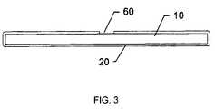
- FIG. 3is a diagram illustrating a cross section view of the semiconductor die showing the conformal coating and openings in the conformal coating above the original connection pads which run down the center of the semiconductor die.
- FIG. 4shows a semiconductor die with connection pads around the periphery of the die.
- FIG. 5shows a semiconductor die with peripheral pads, either original or relocated, coated with a conformal insulative coating, and with openings in the insulative coating located above the peripherally located electrical connection pads.
- FIG. 6is a cross section drawing of a completed 4-high stack on BGA.
- semiconductor die 10with original connection pads 60 have had an insulating layer applied to the top surface, 30 of all of the die while the die are still connected together in a wafer form.
- a metal layeris deposited and defined using photolithography, to reroute the electrical signals from the original connection pads 60 to new locations at the edge of the die.
- An additional layer of insulating materialis optionally applied above the metal layer, and openings are made in the top layer of insulating material at the relocated pad locations at the edge of the semiconductor die, and optionally at the original pad locations down the center of the top surface of the die.
- the semiconductor die, 10has been thinned by grinding or lapping, and has been singulated from the semiconductor wafer, and said semiconductor die has been coated with a conformal insulating coating 20 .
- openingshave been made in the coating, 20 , above original connection pads, 60 , of semiconductor die, 10 .
- thisshows a semiconductor die 70 with connection pads 80 located around the periphery of the die top surface.
- thisshows openings in the conformal coating material at locations 90 on a semiconductor die whose electrical connections are located at the edges of the surface of the die.
- FIG. 6depicts the vertical stack assembly component 5 , consisting of semiconductor die 10 , with conformal coating 20 .
- the semiconductor die 10having metallic conducting elements 61 , one end of which are connected to electrical connection points at the periphery of the die 10 , and the other end of the metallic conducting elements are embedded in the vertical conducting polymer 50 .
- the vertical conductive polymer 50is adjacent to the edge of the stack of the die and electrically connects the die to the top electrical conducting surface, 94 , on the substrate 7 .
- the epoxy perform 30used to laminate the die 10 to each other in a stack by bonding to the conformal coating 20 on each of the die.
- FIG. 6shows the stack of die 10 laminated to each otherwith epoxy perform 30 , and connected electrically by horizontal conducting elements 60 to vertical conducting element 50 and mounted on substrate 7 .
- the substrateis shown having conducting layers 94 on its top and bottom surface, a core 70 , solder mask 92 on the bottom surface, and solder balls 80 connected to the bottom of the substrate. Additionally, an underfill material 40 has been applied so that it fills the space between the bottom die in the stack and the substrate, 70 , forms a filet with the edge of the stack, and fills in the gap between layers from the edge of the perform 30 to the edge of the die.
- the present inventioncan comprise a stack of semiconductor or integrated circuit die mounted on a substrate and laminated to each other.
- the diecan optionally have one or more metal rerouting layers to interconnect the original die connection pads with new connection locations at the edge of the top surface of the die.
- the new connection locationsare desirable for vertical interconnection.
- the diecan have a conformal, insulating coating, where the coating can be a polymer.
- the polymer coatingcan parylene, and the insulating coating can have openings above specific new connection locations at the edge of the top surface of the die as required by the specific component design.
- the openingscan be made, for example, by removing the polymer with laser ablation, and by removing the polymer with a plasma etcher.
- the openingscan be made by preventing the deposition of the polymer coating in selective areas above connection pads on the die.
- the diecan be laminated on top of each other with an electrically insulating polymer or epoxy preform.
- the insulating preformcan be thermally conductive.
- the insulating preformoptionally can include spheres to maintain a fixed spacing or separation between the semiconductor die after lamination.
- the spherescan be made of glass, ceramic, quartz, plastic, Teflon, polymer, or having a metal coating.
- the electrically insulating polymercan be an epoxy.
- the diecan be laminated on top of each other with a liquid polymer that is cured to form a solid bond between the layers in the stack.
- the insulating polymercan optionally include spheres to maintain a fixed spacing or separation between the semiconductor die after lamination, where the spheres can be made of glass, ceramic, quartz, plastic, Teflon, a polymer, and/or a metal coating.
- the electrically insulating polymercan consist of epoxy, where the die can be any semiconductor die, such as memory die, where the memory die can be SDRAM, DDR-1, DDR-2, DDR-3, or any other DRAM.
- the memory diecan be NAND Flash, NOR Flash, M-RAM, F-RAM, E 2 or any other Non-Volatile Memory.
- the memory diecan be SRAM.
- the stackcan be electrically connected vertically, where the vertical electrical connection comprises a conductive polymer.
- the conductive polymercan be a conductive epoxy, such as silver filled (having particles of silver mixed with the polymer), gold filled (having particles of gold mixed with the polymer), the conductive epoxy being filled with metallic particles (having particles of metal mixed with the polymer).
- the electrical connectioncan include one or more metallic conducting elements bonded to the relocated pad locations on the surface of each die and extending, both physically and electrically from the relocated pad into the vertical conductor so that one end of the conductor is embedded within the conductive polymer.
- the metallic conducting elementscan be a bond wire, bond ribbon.
- the metallic conducting elementcan be gold, aluminum, copper, or palladium, on any combination of conducting materials such as gold, aluminum, copper, or palladium.
- the metallic conducting elementscan exist as a metal lead frame with tie bars which is bonded to the die, and after which the tie bars of metal are removed to leave individual metal conducting elements or leads bonded to the connection pads on the die.
- the framecan be formed by excising holes in a thin plate of metal.
- the framecan be cut to remove a center ring or picture frame, leaving behind metal leads ready to attach to the bonding pads on the die, or the frame can be cut to remove an outer ring or picture frame after the leads have been bonded to the connection pads on the die.
- connection padscan be “gang-bonded” simultaneously to the connection pads on the die.
- the electrical connectionscan be used selectively to program, or route unique signals to unique layers of semiconductor die within the stack of semiconductor die as required by the specific component design.
- the electrical connectionscan be connected to the corresponding connection on one or more other die in the stack to connect signals of each of the semiconductor die in the stack in common, as required by the specific component design.
- the electrical connectionscan be fanned out so the similar electrical connections from different die in the stack are available at separate, unique connection points on the module (in other words “not in common”).
- the mounting of the stack of the semiconductor die to the substrateincludes the electrical and physical connection of the vertical interconnects to the aforementioned electrical connection lands on the top surface of said substrate.
- the electrical connectioncan be done with the use of a conductive polymer “dot”, or “puddle” between the vertical interconnect of the stack of die and the substrate.
- the mounting of the stack of the semiconductor die to the substratecan include an under-fill adhesive material between the bottom of the lowest die in the stack and the top surface of the substrate.
- the underfill adhesive materialcan be an electrical insulating material, a thermally conductive material, where the underfill material can cushion and absorb some of the physical stress that will occur as a result of temperature changes during use of the component.
- the underfill materialcan extend past the edge of the bottom die and form a fillet between the bottom die and the substrate.
- the underfill materialcan extend above the bottom die to forming a fillet between the side of the stack of die at any point above the substrate and the surface of the substrate.
- the underfill materialcan extend above the bottom die to the second, third, fourth, or nth die in the stack of die, or to the top of the stack.
- the mounting of the stack to substratecan be with a polymer or epoxy perform between the bottom die in the stack and the substrate.
- the die in the stackcan be “face-up”, “face-down”, or “face to face”.
- the substratecan have multiple conducting layers for signals, ground, and power supply connections, including one or more conducting layers.
- the substratecan include a means for making electrical connection between the bottom of the substrate and a printed circuit board upon which the substrate with stacked die components is attached.
- the substratecan have solder balls or bumps on the bottom for connection to a printed circuit board.
- the substratecan have LGA contacts for connection to a printed circuit board, where the contacts have a gold surface, a solder coated surface, a copper surface, an aluminum surface, a conductive surface (a metal surface).
- the substratecan have flexible interconnect contacts for connection to a printed circuit board, including flat metallic connection pads (lands) for connection to a printed circuit board or for attachment of solder balls or bumps.
- the substratecan have electrical connection pads on the top surface for connection to a stack of semiconductor die.
- the substratecan have electrical interconnection between the pads on the top surface and the solder ball pad, solder bump pads, or flat connection pads (lands) on the bottom of the substrate.
- the substratecan be multi-layer, with one or more extra metal layers between the top and bottom conducting layer, and insulated from the top and bottom conducting layer, and insulated from each other for ground planes, power planes, and other signal connections between circuitry on the top layer and circuitry on the bottom layer of the substrate.
- a multi layer substrateincludes one or more extra metal layers between the top and bottom conducting layers for heat sinking.
- the substratebeing multi layer, can have one or more extra metal layers above or below the top and/or bottom conducting layers for heat sinking.
- the substratecan comprise an organic material, such as BT, FR4, polyimide, or kapton.
- the substratecan be a flexible substrate, such as a flexible tape, or a flexible film.
- the substratecan be made from ceramic material, silicon, a chipscale substrate, where the chipscale substrate is less than or equal to 1.2 times the die dimensions.
- the assemblycan optionally be without any additional coating, molding, or covering over the die, vertical connections, and/or substrate.
- the top die of the assemblycan be covered with a material to block or attenuate light from impinging on and affecting the semiconductor die in the assembly.
- the assemblycan be coated with a conformal polymer, such as parylene, where the conformal coating can be the final coating of the device.
- the conformal coatingcan be applied prior to further encapsulation or transfer molding, such as in the cases where the device will be molded or encapsulated.
- the assemblycan be over-molded with a polymer, plastic, or epoxy to completely coat and cover the stack of semiconductor die and the top of the substrate, leaving the connections at the bottom of the substrate uncovered and exposed for electrical connection.
- the assemblycan be molded in a polymer, plastic, or epoxy to completely cover and seal the stack of semiconductor die and the top surface of the component.
- the moldingcan be a “transfer mold” process.
- the assemblycan be covered by a heatsink, or in a hermetic package.
- the stacked die BGA componentis suitable for high speed circuitry due to the component having low inductance, low capacitance, low DC resistance, and/or matched AC Impedance.
- the componentoptionally can have ground and power planes included in the substrate and or the die.
Landscapes
- Engineering & Computer Science (AREA)
- Microelectronics & Electronic Packaging (AREA)
- Power Engineering (AREA)
- Physics & Mathematics (AREA)
- Condensed Matter Physics & Semiconductors (AREA)
- General Physics & Mathematics (AREA)
- Computer Hardware Design (AREA)
- Manufacturing & Machinery (AREA)
- Encapsulation Of And Coatings For Semiconductor Or Solid State Devices (AREA)
- Wire Bonding (AREA)
Abstract
Description
Claims (92)
Priority Applications (2)
| Application Number | Priority Date | Filing Date | Title |
|---|---|---|---|
| US11/744,142US8357999B2 (en) | 2004-04-13 | 2007-05-03 | Assembly having stacked die mounted on substrate |
| US13/728,246US8729690B2 (en) | 2004-04-13 | 2012-12-27 | Assembly having stacked die mounted on substrate |
Applications Claiming Priority (3)
| Application Number | Priority Date | Filing Date | Title |
|---|---|---|---|
| US56184904P | 2004-04-13 | 2004-04-13 | |
| US11/090,969US7215018B2 (en) | 2004-04-13 | 2005-03-25 | Stacked die BGA or LGA component assembly |
| US11/744,142US8357999B2 (en) | 2004-04-13 | 2007-05-03 | Assembly having stacked die mounted on substrate |
Related Parent Applications (1)
| Application Number | Title | Priority Date | Filing Date |
|---|---|---|---|
| US11/090,969ContinuationUS7215018B2 (en) | 2004-04-13 | 2005-03-25 | Stacked die BGA or LGA component assembly |
Related Child Applications (1)
| Application Number | Title | Priority Date | Filing Date |
|---|---|---|---|
| US13/728,246ContinuationUS8729690B2 (en) | 2004-04-13 | 2012-12-27 | Assembly having stacked die mounted on substrate |
Publications (2)
| Publication Number | Publication Date |
|---|---|
| US20070284716A1 US20070284716A1 (en) | 2007-12-13 |
| US8357999B2true US8357999B2 (en) | 2013-01-22 |
Family
ID=35150640
Family Applications (3)
| Application Number | Title | Priority Date | Filing Date |
|---|---|---|---|
| US11/090,969Expired - Fee RelatedUS7215018B2 (en) | 2004-04-13 | 2005-03-25 | Stacked die BGA or LGA component assembly |
| US11/744,142Expired - Fee RelatedUS8357999B2 (en) | 2004-04-13 | 2007-05-03 | Assembly having stacked die mounted on substrate |
| US13/728,246Expired - LifetimeUS8729690B2 (en) | 2004-04-13 | 2012-12-27 | Assembly having stacked die mounted on substrate |
Family Applications Before (1)
| Application Number | Title | Priority Date | Filing Date |
|---|---|---|---|
| US11/090,969Expired - Fee RelatedUS7215018B2 (en) | 2004-04-13 | 2005-03-25 | Stacked die BGA or LGA component assembly |
Family Applications After (1)
| Application Number | Title | Priority Date | Filing Date |
|---|---|---|---|
| US13/728,246Expired - LifetimeUS8729690B2 (en) | 2004-04-13 | 2012-12-27 | Assembly having stacked die mounted on substrate |
Country Status (5)
| Country | Link |
|---|---|
| US (3) | US7215018B2 (en) |
| EP (1) | EP1763894A2 (en) |
| KR (2) | KR20130038404A (en) |
| TW (1) | TWI389273B (en) |
| WO (1) | WO2005101492A2 (en) |
Cited By (10)
| Publication number | Priority date | Publication date | Assignee | Title |
|---|---|---|---|---|
| US8461672B2 (en) | 2007-07-27 | 2013-06-11 | Tessera, Inc. | Reconstituted wafer stack packaging with after-applied pad extensions |
| US8476774B2 (en) | 2006-10-10 | 2013-07-02 | Tessera, Inc. | Off-chip VIAS in stacked chips |
| US8513794B2 (en) | 2007-08-09 | 2013-08-20 | Tessera, Inc. | Stacked assembly including plurality of stacked microelectronic elements |
| US8551815B2 (en) | 2007-08-03 | 2013-10-08 | Tessera, Inc. | Stack packages using reconstituted wafers |
| US8729690B2 (en)* | 2004-04-13 | 2014-05-20 | Invensas Corporation | Assembly having stacked die mounted on substrate |
| US8829677B2 (en) | 2010-10-14 | 2014-09-09 | Invensas Corporation | Semiconductor die having fine pitch electrical interconnects |
| US8999810B2 (en) | 2006-10-10 | 2015-04-07 | Tessera, Inc. | Method of making a stacked microelectronic package |
| US9159705B2 (en) | 2013-07-11 | 2015-10-13 | Samsung Electronics Co., Ltd. | Semiconductor chip connecting semiconductor package |
| US9356001B2 (en) | 2014-10-02 | 2016-05-31 | HGST Netherlands B.V. | Semiconductor device with at least one voltage-guided conductive filament |
| US10468400B2 (en) | 2017-02-03 | 2019-11-05 | Samsung Electronics Co., Ltd. | Method of manufacturing substrate structure |
Families Citing this family (65)
| Publication number | Priority date | Publication date | Assignee | Title |
|---|---|---|---|---|
| US7245021B2 (en)* | 2004-04-13 | 2007-07-17 | Vertical Circuits, Inc. | Micropede stacked die component assembly |
| US7705432B2 (en)* | 2004-04-13 | 2010-04-27 | Vertical Circuits, Inc. | Three dimensional six surface conformal die coating |
| US7829438B2 (en) | 2006-10-10 | 2010-11-09 | Tessera, Inc. | Edge connect wafer level stacking |
| US8154881B2 (en)* | 2006-11-13 | 2012-04-10 | Telecommunication Systems, Inc. | Radiation-shielded semiconductor assembly |
| US7952195B2 (en) | 2006-12-28 | 2011-05-31 | Tessera, Inc. | Stacked packages with bridging traces |
| US8723332B2 (en) | 2007-06-11 | 2014-05-13 | Invensas Corporation | Electrically interconnected stacked die assemblies |
| WO2008154582A2 (en)* | 2007-06-11 | 2008-12-18 | Vertical Circuits, Inc. | Semiconductor die coating and interconnection fixture and method |
| WO2008154580A2 (en)* | 2007-06-11 | 2008-12-18 | Vertical Circuits, Inc. | Method for optimized integrated circuit chip interconnection |
| WO2008157722A1 (en)* | 2007-06-19 | 2008-12-24 | Vertical Circuits, Inc. | Wafer level surface passivation of stackable integrated circuit chips |
| TW200917391A (en)* | 2007-06-20 | 2009-04-16 | Vertical Circuits Inc | Three-dimensional circuitry formed on integrated circuit device using two-dimensional fabrication |
| SG148901A1 (en) | 2007-07-09 | 2009-01-29 | Micron Technology Inc | Packaged semiconductor assemblies and methods for manufacturing such assemblies |
| JP5110995B2 (en)* | 2007-07-20 | 2012-12-26 | 新光電気工業株式会社 | Multilayer semiconductor device and manufacturing method thereof |
| WO2009026171A2 (en)* | 2007-08-17 | 2009-02-26 | Vertical Circuits, Inc. | Stacked die vertical interconnect formed by transfer of interconnect material |
| US20090068790A1 (en)* | 2007-09-07 | 2009-03-12 | Vertical Circuits, Inc. | Electrical Interconnect Formed by Pulsed Dispense |
| WO2009035849A2 (en) | 2007-09-10 | 2009-03-19 | Vertical Circuits, Inc. | Semiconductor die mount by conformal die coating |
| KR20090034081A (en)* | 2007-10-02 | 2009-04-07 | 삼성전자주식회사 | Multilayer semiconductor package device and manufacturing method thereof |
| WO2009052150A1 (en)* | 2007-10-18 | 2009-04-23 | Vertical Circuits, Inc. | Chip scale stacked die package |
| CN101999167B (en)* | 2008-03-12 | 2013-07-17 | 伊文萨思公司 | Support mounted electrically interconnected die assembly |
| US7863159B2 (en) | 2008-06-19 | 2011-01-04 | Vertical Circuits, Inc. | Semiconductor die separation method |
| US9153517B2 (en) | 2008-05-20 | 2015-10-06 | Invensas Corporation | Electrical connector between die pad and z-interconnect for stacked die assemblies |
| JP5639052B2 (en) | 2008-06-16 | 2014-12-10 | テッセラ,インコーポレイテッド | Edge stacking at wafer level |
| TWI514543B (en)* | 2008-12-09 | 2015-12-21 | Invensas Corp | Semiconductor die interconnect formed by aerosol application of electrically conductive material |
| WO2010068699A2 (en)* | 2008-12-09 | 2010-06-17 | Vertical Circuits, Inc. | Semiconductor die interconnect formed by aerosol application of electrically conductive material |
| JP5112275B2 (en)* | 2008-12-16 | 2013-01-09 | 新光電気工業株式会社 | Semiconductor device and manufacturing method of semiconductor device |
| US8097956B2 (en)* | 2009-03-12 | 2012-01-17 | Apple Inc. | Flexible packaging for chip-on-chip and package-on-package technologies |
| WO2010104610A2 (en) | 2009-03-13 | 2010-09-16 | Tessera Technologies Hungary Kft. | Stacked microelectronic assemblies having vias extending through bond pads |
| US20110115099A1 (en)* | 2009-05-14 | 2011-05-19 | Vertical Circuits, Inc. | Flip-chip underfill |
| US8533853B2 (en) | 2009-06-12 | 2013-09-10 | Telecommunication Systems, Inc. | Location sensitive solid state drive |
| JP5215244B2 (en)* | 2009-06-18 | 2013-06-19 | 新光電気工業株式会社 | Semiconductor device |
| WO2010151578A2 (en) | 2009-06-26 | 2010-12-29 | Vertical Circuits, Inc. | Electrical interconnect for die stacked in zig-zag configuration |
| KR101037827B1 (en)* | 2009-10-06 | 2011-05-30 | 앰코 테크놀로지 코리아 주식회사 | Semiconductor package |
| WO2011056668A2 (en) | 2009-10-27 | 2011-05-12 | Vertical Circuits, Inc. | Selective die electrical insulation additive process |
| TWI544604B (en) | 2009-11-04 | 2016-08-01 | 英維瑟斯公司 | Stacked die assembly having reduced stress electrical interconnects |
| US9136197B2 (en) | 2010-09-16 | 2015-09-15 | Tessera, Inc. | Impedence controlled packages with metal sheet or 2-layer RDL |
| US8853708B2 (en)* | 2010-09-16 | 2014-10-07 | Tessera, Inc. | Stacked multi-die packages with impedance control |
| US8461698B1 (en)* | 2010-09-28 | 2013-06-11 | Rockwell Collins, Inc. | PCB external ground plane via conductive coating |
| US8587088B2 (en)* | 2011-02-17 | 2013-11-19 | Apple Inc. | Side-mounted controller and methods for making the same |
| KR20130027628A (en)* | 2011-06-27 | 2013-03-18 | 삼성전자주식회사 | Stacked semiconductor device |
| KR101887084B1 (en) | 2011-09-22 | 2018-08-10 | 삼성전자주식회사 | Multi-chip semiconductor package and method of forming the same |
| WO2013067270A1 (en) | 2011-11-04 | 2013-05-10 | Invensas Corporation | Bonding wedge |
| TWI459482B (en)* | 2012-01-17 | 2014-11-01 | 矽品精密工業股份有限公司 | Multi-chip stack package structure and method of forming same |
| KR101994930B1 (en) | 2012-11-05 | 2019-07-01 | 삼성전자주식회사 | Semiconductor Package having Integral Unit Semicondudtor Chips |
| US8847412B2 (en) | 2012-11-09 | 2014-09-30 | Invensas Corporation | Microelectronic assembly with thermally and electrically conductive underfill |
| KR101933364B1 (en) | 2013-01-09 | 2018-12-27 | 샌디스크 세미컨덕터 (상하이) 컴퍼니, 리미티드 | Semiconductor device including independent film layer for embedding and/or spacing semiconductor die |
| US9070653B2 (en) | 2013-01-15 | 2015-06-30 | Freescale Semiconductor, Inc. | Microelectronic assembly having a heat spreader for a plurality of die |
| KR20140123129A (en) | 2013-04-10 | 2014-10-22 | 삼성전자주식회사 | Semiconductor Package |
| US9337119B2 (en)* | 2014-07-14 | 2016-05-10 | Micron Technology, Inc. | Stacked semiconductor die assemblies with high efficiency thermal paths and associated systems |
| US9691746B2 (en) | 2014-07-14 | 2017-06-27 | Micron Technology, Inc. | Methods of manufacturing stacked semiconductor die assemblies with high efficiency thermal paths |
| CN105659375B (en)* | 2014-09-26 | 2021-08-24 | 英特尔公司 | Flexible packaging framework |
| US10178786B2 (en) | 2015-05-04 | 2019-01-08 | Honeywell International Inc. | Circuit packages including modules that include at least one integrated circuit |
| US9741644B2 (en)* | 2015-05-04 | 2017-08-22 | Honeywell International Inc. | Stacking arrangement for integration of multiple integrated circuits |
| US9825002B2 (en) | 2015-07-17 | 2017-11-21 | Invensas Corporation | Flipped die stack |
| US9871019B2 (en) | 2015-07-17 | 2018-01-16 | Invensas Corporation | Flipped die stack assemblies with leadframe interconnects |
| US9490195B1 (en) | 2015-07-17 | 2016-11-08 | Invensas Corporation | Wafer-level flipped die stacks with leadframes or metal foil interconnects |
| US9508691B1 (en) | 2015-12-16 | 2016-11-29 | Invensas Corporation | Flipped die stacks with multiple rows of leadframe interconnects |
| US11329026B2 (en)* | 2016-02-17 | 2022-05-10 | Micron Technology, Inc. | Apparatuses and methods for internal heat spreading for packaged semiconductor die |
| US10566310B2 (en) | 2016-04-11 | 2020-02-18 | Invensas Corporation | Microelectronic packages having stacked die and wire bond interconnects |
| US9595511B1 (en) | 2016-05-12 | 2017-03-14 | Invensas Corporation | Microelectronic packages and assemblies with improved flyby signaling operation |
| US9728524B1 (en) | 2016-06-30 | 2017-08-08 | Invensas Corporation | Enhanced density assembly having microelectronic packages mounted at substantial angle to board |
| US10297544B2 (en)* | 2017-09-26 | 2019-05-21 | Taiwan Semiconductor Manufacturing Co., Ltd. | Integrated fan-out package and method of fabricating the same |
| US11224131B2 (en)* | 2018-04-04 | 2022-01-11 | Lenovo (Singapore) Pte. Ltd. | Systems and methods for surface mounting cable connections |
| US10985151B2 (en)* | 2019-04-19 | 2021-04-20 | Nanya Technology Corporation | Semiconductor package and method for preparing the same |
| CN112151514B (en)* | 2019-06-28 | 2025-07-29 | 桑迪士克科技股份有限公司 | Semiconductor device including vertically stacked semiconductor die |
| US11456272B2 (en)* | 2020-09-11 | 2022-09-27 | Western Digital Technologies, Inc. | Straight wirebonding of silicon dies |
| KR20240001869A (en)* | 2022-06-28 | 2024-01-04 | 삼성전자주식회사 | Semiconductor package |
Citations (102)
| Publication number | Priority date | Publication date | Assignee | Title |
|---|---|---|---|---|
| US3648131A (en) | 1969-11-07 | 1972-03-07 | Ibm | Hourglass-shaped conductive connection through semiconductor structures |
| US4074342A (en) | 1974-12-20 | 1978-02-14 | International Business Machines Corporation | Electrical package for lsi devices and assembly process therefor |
| US4323914A (en) | 1979-02-01 | 1982-04-06 | International Business Machines Corporation | Heat transfer structure for integrated circuit package |
| US4525921A (en) | 1981-07-13 | 1985-07-02 | Irvine Sensors Corporation | High-density electronic processing package-structure and fabrication |
| US4545840A (en) | 1983-03-08 | 1985-10-08 | Monolithic Memories, Inc. | Process for controlling thickness of die attach adhesive |
| US4646128A (en) | 1980-09-16 | 1987-02-24 | Irvine Sensors Corporation | High-density electronic processing package--structure and fabrication |
| US4659931A (en) | 1985-05-08 | 1987-04-21 | Grumman Aerospace Corporation | High density multi-layered integrated circuit package |
| US4672737A (en) | 1984-01-23 | 1987-06-16 | Irvine Sensors Corporation | Detector array module fabrication process |
| US4703170A (en) | 1985-04-12 | 1987-10-27 | Grumman Aerospace Corporation | Infrared focal plane module |
| US4706166A (en) | 1986-04-25 | 1987-11-10 | Irvine Sensors Corporation | High-density electronic modules--process and product |
| US4761681A (en) | 1982-09-08 | 1988-08-02 | Texas Instruments Incorporated | Method for fabricating a semiconductor contact and interconnect structure using orientation dependent etching and thermomigration |
| US4764846A (en) | 1987-01-05 | 1988-08-16 | Irvine Sensors Corporation | High density electronic package comprising stacked sub-modules |
| US4818823A (en) | 1987-07-06 | 1989-04-04 | Micro-Circuits, Inc. | Adhesive component means for attaching electrical components to conductors |
| US4862249A (en) | 1987-04-17 | 1989-08-29 | Xoc Devices, Inc. | Packaging system for stacking integrated circuits |
| US4894706A (en) | 1985-02-14 | 1990-01-16 | Nippon Telegraph And Telephone Corporation | Three-dimensional packaging of semiconductor device chips |
| US4897708A (en) | 1986-07-17 | 1990-01-30 | Laser Dynamics, Inc. | Semiconductor wafer array |
| US4939568A (en) | 1986-03-20 | 1990-07-03 | Fujitsu Limited | Three-dimensional integrated circuit and manufacturing method thereof |
| US4941033A (en) | 1988-12-27 | 1990-07-10 | Mitsubishi Denki Kabushiki Kaisha | Semiconductor integrated circuit device |
| US4953005A (en) | 1987-04-17 | 1990-08-28 | Xoc Devices, Inc. | Packaging system for stacking integrated circuits |
| US4954875A (en) | 1986-07-17 | 1990-09-04 | Laser Dynamics, Inc. | Semiconductor wafer array with electrically conductive compliant material |
| US4956695A (en) | 1989-05-12 | 1990-09-11 | Rockwell International Corporation | Three-dimensional packaging of focal plane assemblies using ceramic spacers |
| US4956694A (en) | 1988-11-04 | 1990-09-11 | Dense-Pac Microsystems, Inc. | Integrated circuit chip stacking |
| US4959749A (en) | 1989-08-16 | 1990-09-25 | Unisys Corporation | Layered electronic assembly having compensation for chips of different thickness and different I/O lead offsets |
| US4983533A (en) | 1987-10-28 | 1991-01-08 | Irvine Sensors Corporation | High-density electronic modules - process and product |
| US4996583A (en) | 1989-02-15 | 1991-02-26 | Matsushita Electric Industrial Co., Ltd. | Stack type semiconductor package |
| US5013687A (en) | 1989-07-27 | 1991-05-07 | Grumman Aerospace Corporation | Framed chip hybrid stacked layer assembly |
| US5019943A (en) | 1990-02-14 | 1991-05-28 | Unisys Corporation | High density chip stack having a zigzag-shaped face which accommodates connections between chips |
| US5025306A (en) | 1988-08-09 | 1991-06-18 | Texas Instruments Incorporated | Assembly of semiconductor chips |
| US5028986A (en) | 1987-12-28 | 1991-07-02 | Hitachi, Ltd. | Semiconductor device and semiconductor module with a plurality of stacked semiconductor devices |
| US5075253A (en) | 1989-04-12 | 1991-12-24 | Advanced Micro Devices, Inc. | Method of coplanar integration of semiconductor IC devices |
| US5093708A (en) | 1990-08-20 | 1992-03-03 | Grumman Aerospace Corporation | Multilayer integrated circuit module |
| US5104820A (en) | 1989-07-07 | 1992-04-14 | Irvine Sensors Corporation | Method of fabricating electronic circuitry unit containing stacked IC layers having lead rerouting |
| US5111278A (en) | 1991-03-27 | 1992-05-05 | Eichelberger Charles W | Three-dimensional multichip module systems |
| US5117282A (en) | 1990-10-29 | 1992-05-26 | Harris Corporation | Stacked configuration for integrated circuit devices |
| US5135556A (en) | 1991-04-08 | 1992-08-04 | Grumman Aerospace Corporation | Method for making fused high density multi-layer integrated circuit module |
| US5138437A (en) | 1987-07-27 | 1992-08-11 | Mitsubishi Denki Kabushiki Kaisha | Semiconductor integrated circuit device in which integrated circuit units having different functions are stacked in three dimensional manner |
| US5146308A (en) | 1990-10-05 | 1992-09-08 | Micron Technology, Inc. | Semiconductor package utilizing edge connected semiconductor dice |
| US5172303A (en) | 1990-11-23 | 1992-12-15 | Motorola, Inc. | Electronic component assembly |
| US5191405A (en) | 1988-12-23 | 1993-03-02 | Matsushita Electric Industrial Co., Ltd. | Three-dimensional stacked lsi |
| US5198888A (en) | 1987-12-28 | 1993-03-30 | Hitachi, Ltd. | Semiconductor stacked device |
| US5202754A (en) | 1991-09-13 | 1993-04-13 | International Business Machines Corporation | Three-dimensional multichip packages and methods of fabrication |
| US5221642A (en) | 1991-08-15 | 1993-06-22 | Staktek Corporation | Lead-on-chip integrated circuit fabrication method |
| US5222014A (en) | 1992-03-02 | 1993-06-22 | Motorola, Inc. | Three-dimensional multi-chip pad array carrier |
| US5229647A (en) | 1991-03-27 | 1993-07-20 | Micron Technology, Inc. | High density data storage using stacked wafers |
| US5231304A (en) | 1989-07-27 | 1993-07-27 | Grumman Aerospace Corporation | Framed chip hybrid stacked layer assembly |
| US5247423A (en) | 1992-05-26 | 1993-09-21 | Motorola, Inc. | Stacking three dimensional leadless multi-chip module and method for making the same |
| US5258330A (en) | 1990-09-24 | 1993-11-02 | Tessera, Inc. | Semiconductor chip assemblies with fan-in leads |
| US5270261A (en) | 1991-09-13 | 1993-12-14 | International Business Machines Corporation | Three dimensional multichip package methods of fabrication |
| US5270571A (en) | 1991-10-30 | 1993-12-14 | Amdahl Corporation | Three-dimensional package for semiconductor devices |
| US5279029A (en) | 1990-08-01 | 1994-01-18 | Staktek Corporation | Ultra high density integrated circuit packages method |
| US5309326A (en) | 1991-12-06 | 1994-05-03 | Rohm Co., Ltd. | Circuit module having stacked circuit boards |
| US5311401A (en) | 1991-07-09 | 1994-05-10 | Hughes Aircraft Company | Stacked chip assembly and manufacturing method therefor |
| US5313096A (en) | 1992-03-16 | 1994-05-17 | Dense-Pac Microsystems, Inc. | IC chip package having chip attached to and wire bonded within an overlying substrate |
| US5330359A (en) | 1993-03-26 | 1994-07-19 | The Whitaker Corporation | Socket for stacking integrated circuit chips |
| US5422435A (en) | 1992-05-22 | 1995-06-06 | National Semiconductor Corporation | Stacked multi-chip modules and method of manufacturing |
| US5434745A (en) | 1994-07-26 | 1995-07-18 | White Microelectronics Div. Of Bowmar Instrument Corp. | Stacked silicon die carrier assembly |
| US5445994A (en) | 1994-04-11 | 1995-08-29 | Micron Technology, Inc. | Method for forming custom planar metal bonding pad connectors for semiconductor dice |
| US5446620A (en) | 1990-08-01 | 1995-08-29 | Staktek Corporation | Ultra high density integrated circuit packages |
| US5479318A (en) | 1994-03-07 | 1995-12-26 | Staktek Corporation | Bus communication system for stacked high density integrated circuit packages with trifurcated distal lead ends |
| US5499160A (en) | 1990-08-01 | 1996-03-12 | Staktek Corporation | High density integrated circuit module with snap-on rail assemblies |
| US5502333A (en) | 1994-03-30 | 1996-03-26 | International Business Machines Corporation | Semiconductor stack structures and fabrication/sparing methods utilizing programmable spare circuit |
| US5538758A (en) | 1995-10-27 | 1996-07-23 | Specialty Coating Systems, Inc. | Method and apparatus for the deposition of parylene AF4 onto semiconductor wafers |
| US5600541A (en) | 1993-12-08 | 1997-02-04 | Hughes Aircraft Company | Vertical IC chip stack with discrete chip carriers formed from dielectric tape |
| US5616953A (en)* | 1994-09-01 | 1997-04-01 | Micron Technology, Inc. | Lead frame surface finish enhancement |
| US5625230A (en) | 1994-12-28 | 1997-04-29 | Samsung Display Devices Co., Ltd. | Integrated circuit chip structure |
| US5657206A (en) | 1994-06-23 | 1997-08-12 | Cubic Memory, Inc. | Conductive epoxy flip-chip package and method |
| US5675180A (en) | 1994-06-23 | 1997-10-07 | Cubic Memory, Inc. | Vertical interconnect process for silicon segments |
| US5688721A (en) | 1994-03-15 | 1997-11-18 | Irvine Sensors Corporation | 3D stack of IC chips having leads reached by vias through passivation covering access plane |
| US5696031A (en) | 1996-11-20 | 1997-12-09 | Micron Technology, Inc. | Device and method for stacking wire-bonded integrated circuit dice on flip-chip bonded integrated circuit dice |
| US5698895A (en) | 1994-06-23 | 1997-12-16 | Cubic Memory, Inc. | Silicon segment programming method and apparatus |
| US5724230A (en) | 1996-06-21 | 1998-03-03 | International Business Machines Corporation | Flexible laminate module including spacers embedded in an adhesive |
| US5870351A (en) | 1994-10-21 | 1999-02-09 | The Board Of Trustees Of The Leland Stanford Junior University | Broadband microfabriated ultrasonic transducer and method of fabrication |
| US5879965A (en)* | 1997-06-19 | 1999-03-09 | Micron Technology, Inc. | Plastic lead frames for semiconductor devices, packages including same, and methods of fabrication |
| US5891761A (en) | 1994-06-23 | 1999-04-06 | Cubic Memory, Inc. | Method for forming vertical interconnect process for silicon segments with thermally conductive epoxy preform |
| US6080596A (en) | 1994-06-23 | 2000-06-27 | Cubic Memory Inc. | Method for forming vertical interconnect process for silicon segments with dielectric isolation |
| US6107164A (en) | 1998-08-18 | 2000-08-22 | Oki Electric Industry Co., Ltd. | Using grooves as alignment marks when dicing an encapsulated semiconductor wafer |
| US6124633A (en) | 1994-06-23 | 2000-09-26 | Cubic Memory | Vertical interconnect process for silicon segments with thermally conductive epoxy preform |
| US6255726B1 (en) | 1994-06-23 | 2001-07-03 | Cubic Memory, Inc. | Vertical interconnect process for silicon segments with dielectric isolation |
| US6271598B1 (en)* | 1997-07-29 | 2001-08-07 | Cubic Memory, Inc. | Conductive epoxy flip-chip on chip |
| US6297657B1 (en) | 1999-01-11 | 2001-10-02 | Wentworth Laboratories, Inc. | Temperature compensated vertical pin probing device |
| US6303977B1 (en) | 1998-12-03 | 2001-10-16 | Texas Instruments Incorporated | Fully hermetic semiconductor chip, including sealed edge sides |
| US20010031548A1 (en) | 1997-10-20 | 2001-10-18 | Peter Elenius | Method for forming chip scale package |
| US6338980B1 (en) | 1999-08-13 | 2002-01-15 | Citizen Watch Co., Ltd. | Method for manufacturing chip-scale package and manufacturing IC chip |
| US6351030B2 (en) | 1997-09-29 | 2002-02-26 | International Business Machines Corporation | Electronic package utilizing protective coating |
| US20020168798A1 (en) | 1996-10-31 | 2002-11-14 | Glenn Thomas P. | Method of making near chip size integrated circuit package |
| US20020187260A1 (en) | 2001-05-30 | 2002-12-12 | Sheppard Norman F. | Conformal coated microchip reservoir devices |
| US20020185725A1 (en)* | 1998-08-21 | 2002-12-12 | Moden Walter L. | Low profile multi-IC chip package connector |
| US20030099085A1 (en) | 2001-11-26 | 2003-05-29 | Delaware Capital Formation, Inc. | Surface flashover resistant capacitors and method for producing same |
| US6664616B2 (en) | 1996-11-21 | 2003-12-16 | Hitachi, Ltd. | Semiconductor device and manufacturing method thereof |
| US6667543B1 (en) | 2002-10-29 | 2003-12-23 | Motorola, Inc. | Optical sensor package |
| US6674159B1 (en) | 2000-05-16 | 2004-01-06 | Sandia National Laboratories | Bi-level microelectronic device package with an integral window |
| US20040150095A1 (en)* | 2003-01-30 | 2004-08-05 | Endicott Interconnect Technologies, Inc. | Stacked chip electronic package having laminate carrier and method of making same |
| US20040195667A1 (en)* | 2003-04-04 | 2004-10-07 | Chippac, Inc | Semiconductor multipackage module including processor and memory package assemblies |
| US6844623B1 (en) | 2000-05-16 | 2005-01-18 | Sandia Corporation | Temporary coatings for protection of microelectronic devices during packaging |
| US20050082651A1 (en) | 2003-10-20 | 2005-04-21 | Farnworth Warren M. | Methods of coating and singulating wafers and chip-scale packages formed therefrom |
| US6908784B1 (en) | 2002-03-06 | 2005-06-21 | Micron Technology, Inc. | Method for fabricating encapsulated semiconductor components |
| US6940022B1 (en) | 1997-12-18 | 2005-09-06 | Vlt, Inc. | Protective coating for an electronic device |
| US6956283B1 (en) | 2000-05-16 | 2005-10-18 | Peterson Kenneth A | Encapsulants for protecting MEMS devices during post-packaging release etch |
| US6984885B1 (en) | 2000-02-10 | 2006-01-10 | Renesas Technology Corp. | Semiconductor device having densely stacked semiconductor chips |
| US7091592B2 (en) | 2003-05-27 | 2006-08-15 | Industrial Technology Research Institute | Stacked package for electronic elements and packaging method thereof |
| EP1763894A2 (en) | 2004-04-13 | 2007-03-21 | Vertical Circuits, Inc. | Stacked die bga or lga component assembly |
| US7245021B2 (en)* | 2004-04-13 | 2007-07-17 | Vertical Circuits, Inc. | Micropede stacked die component assembly |
Family Cites Families (70)
| Publication number | Priority date | Publication date | Assignee | Title |
|---|---|---|---|---|
| US3702025A (en) | 1969-05-12 | 1972-11-07 | Honeywell Inc | Discretionary interconnection process |
| US3679941A (en) | 1969-09-22 | 1972-07-25 | Gen Electric | Composite integrated circuits including semiconductor chips mounted on a common substrate with connections made through a dielectric encapsulator |
| US4500905A (en) | 1981-09-30 | 1985-02-19 | Tokyo Shibaura Denki Kabushiki Kaisha | Stacked semiconductor device with sloping sides |
| JPS61239649A (en) | 1985-04-13 | 1986-10-24 | Fujitsu Ltd | High speed integrated circuit package |
| US4807021A (en) | 1986-03-10 | 1989-02-21 | Kabushiki Kaisha Toshiba | Semiconductor device having stacking structure |
| JPH0680878B2 (en) | 1986-08-27 | 1994-10-12 | 日本電気株式会社 | Integrated circuit |
| US4801992A (en) | 1986-12-01 | 1989-01-31 | Motorola Inc. | Three dimensional interconnected integrated circuit |
| US4901136A (en) | 1987-07-14 | 1990-02-13 | General Electric Company | Multi-chip interconnection package |
| JPS6435528U (en) | 1987-08-22 | 1989-03-03 | ||
| JPH02133936A (en) | 1988-11-15 | 1990-05-23 | Seiko Epson Corp | semiconductor equipment |
| US5032896A (en) | 1989-08-31 | 1991-07-16 | Hughes Aircraft Company | 3-D integrated circuit assembly employing discrete chips |
| US5006923A (en) | 1989-09-14 | 1991-04-09 | Litton Systems, Inc. | Stackable multilayer substrate for mounting integrated circuits |
| US5128831A (en) | 1991-10-31 | 1992-07-07 | Micron Technology, Inc. | High-density electronic package comprising stacked sub-modules which are electrically interconnected by solder-filled vias |
| WO1993023982A1 (en) | 1992-05-11 | 1993-11-25 | Nchip, Inc. | Stacked devices for multichip modules |
| FR2704690B1 (en) | 1993-04-27 | 1995-06-23 | Thomson Csf | Method for encapsulating semiconductor wafers, device obtained by this process and application to the interconnection of wafers in three dimensions. |
| US6228686B1 (en) | 1995-09-18 | 2001-05-08 | Tessera, Inc. | Method of fabricating a microelectronic assembly using sheets with gaps to define lead regions |
| US5466634A (en) | 1994-12-20 | 1995-11-14 | International Business Machines Corporation | Electronic modules with interconnected surface metallization layers and fabrication methods therefore |
| US5648684A (en) | 1995-07-26 | 1997-07-15 | International Business Machines Corporation | Endcap chip with conductive, monolithic L-connect for multichip stack |
| US6784023B2 (en) | 1996-05-20 | 2004-08-31 | Micron Technology, Inc. | Method of fabrication of stacked semiconductor devices |
| EP1029360A4 (en) | 1997-08-21 | 2006-04-12 | Vertical Circuits Inc | VERTICAL INTERMEDIATE CONNECTION METHOD FOR SILICON SEGMENTS WITH DIELECTRIC INSULATION |
| EP1041624A1 (en) | 1999-04-02 | 2000-10-04 | Interuniversitair Microelektronica Centrum Vzw | Method of transferring ultra-thin substrates and application of the method to the manufacture of a multilayer thin film device |
| US6376904B1 (en) | 1999-12-23 | 2002-04-23 | Rambus Inc. | Redistributed bond pads in stacked integrated circuit die package |
| US6621155B1 (en) | 1999-12-23 | 2003-09-16 | Rambus Inc. | Integrated circuit device having stacked dies and impedance balanced transmission lines |
| JP3879351B2 (en) | 2000-01-27 | 2007-02-14 | セイコーエプソン株式会社 | Manufacturing method of semiconductor chip |
| ES2420279T3 (en) | 2000-03-02 | 2013-08-23 | Microchips, Inc. | Microfabricated devices and methods for storage and selective exposure of chemicals |
| US7115986B2 (en) | 2001-05-02 | 2006-10-03 | Micron Technology, Inc. | Flexible ball grid array chip scale packages |
| JP2002359346A (en)* | 2001-05-30 | 2002-12-13 | Sharp Corp | Semiconductor device and method of stacking semiconductor chips |
| KR100394808B1 (en) | 2001-07-19 | 2003-08-14 | 삼성전자주식회사 | Wafer level stack chip package and method for manufacturing the same |
| US6611052B2 (en) | 2001-11-16 | 2003-08-26 | Micron Technology, Inc. | Wafer level stackable semiconductor package |
| JP2003163324A (en) | 2001-11-27 | 2003-06-06 | Nec Corp | Unit semiconductor device and manufacturing method thereof, and three-dimensional laminated semiconductor device |
| TW544882B (en) | 2001-12-31 | 2003-08-01 | Megic Corp | Chip package structure and process thereof |
| US6607941B2 (en) | 2002-01-11 | 2003-08-19 | National Semiconductor Corporation | Process and structure improvements to shellcase style packaging technology |
| US7340181B1 (en) | 2002-05-13 | 2008-03-04 | National Semiconductor Corporation | Electrical die contact structure and fabrication method |
| US6838761B2 (en)* | 2002-09-17 | 2005-01-04 | Chippac, Inc. | Semiconductor multi-package module having wire bond interconnect between stacked packages and having electrical shield |
| JP4081666B2 (en) | 2002-09-24 | 2008-04-30 | セイコーエプソン株式会社 | Semiconductor device and manufacturing method thereof, circuit board, and electronic apparatus |
| US6656827B1 (en) | 2002-10-17 | 2003-12-02 | Taiwan Semiconductor Manufacturing Co., Ltd. | Electrical performance enhanced wafer level chip scale package with ground |
| TWI227550B (en) | 2002-10-30 | 2005-02-01 | Sanyo Electric Co | Semiconductor device manufacturing method |
| JP2004153130A (en) | 2002-10-31 | 2004-05-27 | Olympus Corp | Semiconductor device and its manufacturing method |
| JP2004158536A (en) | 2002-11-05 | 2004-06-03 | Fujitsu Ltd | Semiconductor device and method of manufacturing semiconductor device |
| WO2004109771A2 (en) | 2003-06-03 | 2004-12-16 | Casio Computer Co., Ltd. | Stackable semiconductor device and method of manufacturing the same |
| US6972480B2 (en) | 2003-06-16 | 2005-12-06 | Shellcase Ltd. | Methods and apparatus for packaging integrated circuit devices |
| CN100587962C (en) | 2003-07-03 | 2010-02-03 | 泰塞拉技术匈牙利公司 | Method and apparatus for packaging integrated circuit devices |
| SG120123A1 (en) | 2003-09-30 | 2006-03-28 | Micron Technology Inc | Castellated chip-scale packages and methods for fabricating the same |
| JP4198072B2 (en) | 2004-01-23 | 2008-12-17 | シャープ株式会社 | Semiconductor device, module for optical device, and method for manufacturing semiconductor device |
| DE102004008135A1 (en) | 2004-02-18 | 2005-09-22 | Infineon Technologies Ag | Semiconductor device with a stack of semiconductor chips and method for producing the same |
| JP3811160B2 (en) | 2004-03-09 | 2006-08-16 | 株式会社東芝 | Semiconductor device |
| US7239020B2 (en) | 2004-05-06 | 2007-07-03 | Avago Technologies Wireless Ip (Singapore) Pte. Ltd. | Multi-mode integrated circuit structure |
| TWI236110B (en) | 2004-06-25 | 2005-07-11 | Advanced Semiconductor Eng | Flip chip on leadframe package and method for manufacturing the same |
| DE102004039906A1 (en) | 2004-08-18 | 2005-08-18 | Infineon Technologies Ag | Electronic component with a number of integrated members, is formed by producing members with a surface that contains a circuit, and connecting components using bond wires |
| CN100539135C (en) | 2004-09-08 | 2009-09-09 | 松下电器产业株式会社 | Three-dimensional circuit device, the e-machine that uses it and manufacture method thereof |
| TWI288448B (en) | 2004-09-10 | 2007-10-11 | Toshiba Corp | Semiconductor device and method of manufacturing the same |
| DE102004052921A1 (en) | 2004-10-29 | 2006-05-11 | Infineon Technologies Ag | Process for the production of semiconductor devices with external contacts |
| KR100626618B1 (en) | 2004-12-10 | 2006-09-25 | 삼성전자주식회사 | Semiconductor chip stack package and manufacturing method |
| US20060138626A1 (en) | 2004-12-29 | 2006-06-29 | Tessera, Inc. | Microelectronic packages using a ceramic substrate having a window and a conductive surface region |
| US7326592B2 (en) | 2005-04-04 | 2008-02-05 | Infineon Technologies Ag | Stacked die package |
| US7208345B2 (en) | 2005-05-11 | 2007-04-24 | Infineon Technologies Ag | Method of manufacturing a semiconductor device comprising stacked chips and a corresponding semiconductor device |
| KR100629498B1 (en) | 2005-07-15 | 2006-09-28 | 삼성전자주식회사 | Micro-Packages, Multi-Stack Micro-Packages, and Methods for Making the Same |
| US7981726B2 (en) | 2005-12-12 | 2011-07-19 | Intel Corporation | Copper plating connection for multi-die stack in substrate package |
| US20070158807A1 (en) | 2005-12-29 | 2007-07-12 | Daoqiang Lu | Edge interconnects for die stacking |
| SG135074A1 (en) | 2006-02-28 | 2007-09-28 | Micron Technology Inc | Microelectronic devices, stacked microelectronic devices, and methods for manufacturing such devices |
| US7901989B2 (en) | 2006-10-10 | 2011-03-08 | Tessera, Inc. | Reconstituted wafer level stacking |
| US8513789B2 (en) | 2006-10-10 | 2013-08-20 | Tessera, Inc. | Edge connect wafer level stacking with leads extending along edges |
| US7829438B2 (en) | 2006-10-10 | 2010-11-09 | Tessera, Inc. | Edge connect wafer level stacking |
| US7638869B2 (en) | 2007-03-28 | 2009-12-29 | Qimonda Ag | Semiconductor device |
| KR100914977B1 (en) | 2007-06-18 | 2009-09-02 | 주식회사 하이닉스반도체 | Method for fabricating stack package |
| JP5572089B2 (en) | 2007-07-27 | 2014-08-13 | テッセラ,インコーポレイテッド | Reconfigured wafer stack packaging with pad extension after application |
| US8551815B2 (en) | 2007-08-03 | 2013-10-08 | Tessera, Inc. | Stack packages using reconstituted wafers |
| WO2009052150A1 (en) | 2007-10-18 | 2009-04-23 | Vertical Circuits, Inc. | Chip scale stacked die package |
| CN101999167B (en) | 2008-03-12 | 2013-07-17 | 伊文萨思公司 | Support mounted electrically interconnected die assembly |
| JP5639052B2 (en) | 2008-06-16 | 2014-12-10 | テッセラ,インコーポレイテッド | Edge stacking at wafer level |
- 2005
- 2005-03-25USUS11/090,969patent/US7215018B2/ennot_activeExpired - Fee Related
- 2005-04-11TWTW094111358Apatent/TWI389273B/ennot_activeIP Right Cessation
- 2005-04-12KRKR1020137005143Apatent/KR20130038404A/ennot_activeAbandoned
- 2005-04-12WOPCT/US2005/012412patent/WO2005101492A2/enactiveApplication Filing
- 2005-04-12EPEP05736405Apatent/EP1763894A2/ennot_activeWithdrawn
- 2005-04-12KRKR1020067023775Apatent/KR101277429B1/ennot_activeExpired - Fee Related
- 2007
- 2007-05-03USUS11/744,142patent/US8357999B2/ennot_activeExpired - Fee Related
- 2012
- 2012-12-27USUS13/728,246patent/US8729690B2/ennot_activeExpired - Lifetime
Patent Citations (120)
| Publication number | Priority date | Publication date | Assignee | Title |
|---|---|---|---|---|
| US3648131A (en) | 1969-11-07 | 1972-03-07 | Ibm | Hourglass-shaped conductive connection through semiconductor structures |
| US4074342A (en) | 1974-12-20 | 1978-02-14 | International Business Machines Corporation | Electrical package for lsi devices and assembly process therefor |
| US4323914A (en) | 1979-02-01 | 1982-04-06 | International Business Machines Corporation | Heat transfer structure for integrated circuit package |
| US4646128A (en) | 1980-09-16 | 1987-02-24 | Irvine Sensors Corporation | High-density electronic processing package--structure and fabrication |
| US4525921A (en) | 1981-07-13 | 1985-07-02 | Irvine Sensors Corporation | High-density electronic processing package-structure and fabrication |
| US4761681A (en) | 1982-09-08 | 1988-08-02 | Texas Instruments Incorporated | Method for fabricating a semiconductor contact and interconnect structure using orientation dependent etching and thermomigration |
| US4545840A (en) | 1983-03-08 | 1985-10-08 | Monolithic Memories, Inc. | Process for controlling thickness of die attach adhesive |
| US4672737A (en) | 1984-01-23 | 1987-06-16 | Irvine Sensors Corporation | Detector array module fabrication process |
| US4894706A (en) | 1985-02-14 | 1990-01-16 | Nippon Telegraph And Telephone Corporation | Three-dimensional packaging of semiconductor device chips |
| US4703170A (en) | 1985-04-12 | 1987-10-27 | Grumman Aerospace Corporation | Infrared focal plane module |
| US4659931A (en) | 1985-05-08 | 1987-04-21 | Grumman Aerospace Corporation | High density multi-layered integrated circuit package |
| US4939568A (en) | 1986-03-20 | 1990-07-03 | Fujitsu Limited | Three-dimensional integrated circuit and manufacturing method thereof |
| US4706166A (en) | 1986-04-25 | 1987-11-10 | Irvine Sensors Corporation | High-density electronic modules--process and product |
| US4954875A (en) | 1986-07-17 | 1990-09-04 | Laser Dynamics, Inc. | Semiconductor wafer array with electrically conductive compliant material |
| US4897708A (en) | 1986-07-17 | 1990-01-30 | Laser Dynamics, Inc. | Semiconductor wafer array |
| US4764846A (en) | 1987-01-05 | 1988-08-16 | Irvine Sensors Corporation | High density electronic package comprising stacked sub-modules |
| US4953005A (en) | 1987-04-17 | 1990-08-28 | Xoc Devices, Inc. | Packaging system for stacking integrated circuits |
| US4862249A (en) | 1987-04-17 | 1989-08-29 | Xoc Devices, Inc. | Packaging system for stacking integrated circuits |
| US4818823A (en) | 1987-07-06 | 1989-04-04 | Micro-Circuits, Inc. | Adhesive component means for attaching electrical components to conductors |
| US5138437A (en) | 1987-07-27 | 1992-08-11 | Mitsubishi Denki Kabushiki Kaisha | Semiconductor integrated circuit device in which integrated circuit units having different functions are stacked in three dimensional manner |
| EP0314437B1 (en) | 1987-10-28 | 1992-07-15 | Laser Dynamics, Inc. | Semiconductor wafer array |
| US4983533A (en) | 1987-10-28 | 1991-01-08 | Irvine Sensors Corporation | High-density electronic modules - process and product |
| US5028986A (en) | 1987-12-28 | 1991-07-02 | Hitachi, Ltd. | Semiconductor device and semiconductor module with a plurality of stacked semiconductor devices |
| US5198888A (en) | 1987-12-28 | 1993-03-30 | Hitachi, Ltd. | Semiconductor stacked device |
| US5025306A (en) | 1988-08-09 | 1991-06-18 | Texas Instruments Incorporated | Assembly of semiconductor chips |
| US4956694A (en) | 1988-11-04 | 1990-09-11 | Dense-Pac Microsystems, Inc. | Integrated circuit chip stacking |
| US5191405A (en) | 1988-12-23 | 1993-03-02 | Matsushita Electric Industrial Co., Ltd. | Three-dimensional stacked lsi |
| US4941033A (en) | 1988-12-27 | 1990-07-10 | Mitsubishi Denki Kabushiki Kaisha | Semiconductor integrated circuit device |
| US4996583A (en) | 1989-02-15 | 1991-02-26 | Matsushita Electric Industrial Co., Ltd. | Stack type semiconductor package |
| US5075253A (en) | 1989-04-12 | 1991-12-24 | Advanced Micro Devices, Inc. | Method of coplanar integration of semiconductor IC devices |
| US4956695A (en) | 1989-05-12 | 1990-09-11 | Rockwell International Corporation | Three-dimensional packaging of focal plane assemblies using ceramic spacers |
| US5104820A (en) | 1989-07-07 | 1992-04-14 | Irvine Sensors Corporation | Method of fabricating electronic circuitry unit containing stacked IC layers having lead rerouting |
| US5013687A (en) | 1989-07-27 | 1991-05-07 | Grumman Aerospace Corporation | Framed chip hybrid stacked layer assembly |
| US5231304A (en) | 1989-07-27 | 1993-07-27 | Grumman Aerospace Corporation | Framed chip hybrid stacked layer assembly |
| US4959749A (en) | 1989-08-16 | 1990-09-25 | Unisys Corporation | Layered electronic assembly having compensation for chips of different thickness and different I/O lead offsets |
| US5019943A (en) | 1990-02-14 | 1991-05-28 | Unisys Corporation | High density chip stack having a zigzag-shaped face which accommodates connections between chips |
| US5550711A (en) | 1990-08-01 | 1996-08-27 | Staktek Corporation | Ultra high density integrated circuit packages |
| US5499160A (en) | 1990-08-01 | 1996-03-12 | Staktek Corporation | High density integrated circuit module with snap-on rail assemblies |
| US5446620A (en) | 1990-08-01 | 1995-08-29 | Staktek Corporation | Ultra high density integrated circuit packages |
| US5566051A (en) | 1990-08-01 | 1996-10-15 | Staktek Corporation | Ultra high density integrated circuit packages method and apparatus |
| US5420751A (en) | 1990-08-01 | 1995-05-30 | Staktek Corporation | Ultra high density modular integrated circuit package |
| US5279029A (en) | 1990-08-01 | 1994-01-18 | Staktek Corporation | Ultra high density integrated circuit packages method |
| US5093708A (en) | 1990-08-20 | 1992-03-03 | Grumman Aerospace Corporation | Multilayer integrated circuit module |
| US5258330A (en) | 1990-09-24 | 1993-11-02 | Tessera, Inc. | Semiconductor chip assemblies with fan-in leads |
| US5146308A (en) | 1990-10-05 | 1992-09-08 | Micron Technology, Inc. | Semiconductor package utilizing edge connected semiconductor dice |
| US5117282A (en) | 1990-10-29 | 1992-05-26 | Harris Corporation | Stacked configuration for integrated circuit devices |
| US5172303A (en) | 1990-11-23 | 1992-12-15 | Motorola, Inc. | Electronic component assembly |
| US5229647A (en) | 1991-03-27 | 1993-07-20 | Micron Technology, Inc. | High density data storage using stacked wafers |
| US5111278A (en) | 1991-03-27 | 1992-05-05 | Eichelberger Charles W | Three-dimensional multichip module systems |
| US5135556A (en) | 1991-04-08 | 1992-08-04 | Grumman Aerospace Corporation | Method for making fused high density multi-layer integrated circuit module |
| US5311401A (en) | 1991-07-09 | 1994-05-10 | Hughes Aircraft Company | Stacked chip assembly and manufacturing method therefor |
| US5221642A (en) | 1991-08-15 | 1993-06-22 | Staktek Corporation | Lead-on-chip integrated circuit fabrication method |
| US5202754A (en) | 1991-09-13 | 1993-04-13 | International Business Machines Corporation | Three-dimensional multichip packages and methods of fabrication |
| US5270261A (en) | 1991-09-13 | 1993-12-14 | International Business Machines Corporation | Three dimensional multichip package methods of fabrication |
| US5270571A (en) | 1991-10-30 | 1993-12-14 | Amdahl Corporation | Three-dimensional package for semiconductor devices |
| US5309326A (en) | 1991-12-06 | 1994-05-03 | Rohm Co., Ltd. | Circuit module having stacked circuit boards |
| US5222014A (en) | 1992-03-02 | 1993-06-22 | Motorola, Inc. | Three-dimensional multi-chip pad array carrier |
| US5313096A (en) | 1992-03-16 | 1994-05-17 | Dense-Pac Microsystems, Inc. | IC chip package having chip attached to and wire bonded within an overlying substrate |
| US5422435A (en) | 1992-05-22 | 1995-06-06 | National Semiconductor Corporation | Stacked multi-chip modules and method of manufacturing |
| US5502289A (en) | 1992-05-22 | 1996-03-26 | National Semiconductor Corporation | Stacked multi-chip modules and method of manufacturing |
| US5495398A (en) | 1992-05-22 | 1996-02-27 | National Semiconductor Corporation | Stacked multi-chip modules and method of manufacturing |
| US5247423A (en) | 1992-05-26 | 1993-09-21 | Motorola, Inc. | Stacking three dimensional leadless multi-chip module and method for making the same |
| US5330359A (en) | 1993-03-26 | 1994-07-19 | The Whitaker Corporation | Socket for stacking integrated circuit chips |
| US5600541A (en) | 1993-12-08 | 1997-02-04 | Hughes Aircraft Company | Vertical IC chip stack with discrete chip carriers formed from dielectric tape |
| US5479318A (en) | 1994-03-07 | 1995-12-26 | Staktek Corporation | Bus communication system for stacked high density integrated circuit packages with trifurcated distal lead ends |
| US5493476A (en) | 1994-03-07 | 1996-02-20 | Staktek Corporation | Bus communication system for stacked high density integrated circuit packages with bifurcated distal lead ends |
| US5552963A (en) | 1994-03-07 | 1996-09-03 | Staktek Corporation | Bus communication system for stacked high density integrated circuit packages |
| US5688721A (en) | 1994-03-15 | 1997-11-18 | Irvine Sensors Corporation | 3D stack of IC chips having leads reached by vias through passivation covering access plane |
| US5502333A (en) | 1994-03-30 | 1996-03-26 | International Business Machines Corporation | Semiconductor stack structures and fabrication/sparing methods utilizing programmable spare circuit |
| US5445994A (en) | 1994-04-11 | 1995-08-29 | Micron Technology, Inc. | Method for forming custom planar metal bonding pad connectors for semiconductor dice |
| US5891761A (en) | 1994-06-23 | 1999-04-06 | Cubic Memory, Inc. | Method for forming vertical interconnect process for silicon segments with thermally conductive epoxy preform |
| US5994170A (en) | 1994-06-23 | 1999-11-30 | Cubic Memory, Inc. | Silicon segment programming method |
| US6255726B1 (en) | 1994-06-23 | 2001-07-03 | Cubic Memory, Inc. | Vertical interconnect process for silicon segments with dielectric isolation |
| US5657206A (en) | 1994-06-23 | 1997-08-12 | Cubic Memory, Inc. | Conductive epoxy flip-chip package and method |
| US5675180A (en) | 1994-06-23 | 1997-10-07 | Cubic Memory, Inc. | Vertical interconnect process for silicon segments |
| US6124633A (en) | 1994-06-23 | 2000-09-26 | Cubic Memory | Vertical interconnect process for silicon segments with thermally conductive epoxy preform |
| US6098278A (en) | 1994-06-23 | 2000-08-08 | Cubic Memory, Inc. | Method for forming conductive epoxy flip-chip on chip |
| US5698895A (en) | 1994-06-23 | 1997-12-16 | Cubic Memory, Inc. | Silicon segment programming method and apparatus |
| US6080596A (en) | 1994-06-23 | 2000-06-27 | Cubic Memory Inc. | Method for forming vertical interconnect process for silicon segments with dielectric isolation |
| US5936302A (en) | 1994-06-23 | 1999-08-10 | Cubic Memory, Inc. | Speaker diaphragm |
| US5434745A (en) | 1994-07-26 | 1995-07-18 | White Microelectronics Div. Of Bowmar Instrument Corp. | Stacked silicon die carrier assembly |
| US5616953A (en)* | 1994-09-01 | 1997-04-01 | Micron Technology, Inc. | Lead frame surface finish enhancement |
| US5870351A (en) | 1994-10-21 | 1999-02-09 | The Board Of Trustees Of The Leland Stanford Junior University | Broadband microfabriated ultrasonic transducer and method of fabrication |
| US5625230A (en) | 1994-12-28 | 1997-04-29 | Samsung Display Devices Co., Ltd. | Integrated circuit chip structure |
| US6134118A (en) | 1995-01-19 | 2000-10-17 | Cubic Memory Inc. | Conductive epoxy flip-chip package and method |
| US5538758A (en) | 1995-10-27 | 1996-07-23 | Specialty Coating Systems, Inc. | Method and apparatus for the deposition of parylene AF4 onto semiconductor wafers |
| US5724230A (en) | 1996-06-21 | 1998-03-03 | International Business Machines Corporation | Flexible laminate module including spacers embedded in an adhesive |
| US20020168798A1 (en) | 1996-10-31 | 2002-11-14 | Glenn Thomas P. | Method of making near chip size integrated circuit package |
| US5696031A (en) | 1996-11-20 | 1997-12-09 | Micron Technology, Inc. | Device and method for stacking wire-bonded integrated circuit dice on flip-chip bonded integrated circuit dice |
| US6664616B2 (en) | 1996-11-21 | 2003-12-16 | Hitachi, Ltd. | Semiconductor device and manufacturing method thereof |
| US5879965A (en)* | 1997-06-19 | 1999-03-09 | Micron Technology, Inc. | Plastic lead frames for semiconductor devices, packages including same, and methods of fabrication |
| US6271598B1 (en)* | 1997-07-29 | 2001-08-07 | Cubic Memory, Inc. | Conductive epoxy flip-chip on chip |
| US6351030B2 (en) | 1997-09-29 | 2002-02-26 | International Business Machines Corporation | Electronic package utilizing protective coating |
| US20010031548A1 (en) | 1997-10-20 | 2001-10-18 | Peter Elenius | Method for forming chip scale package |
| US6940022B1 (en) | 1997-12-18 | 2005-09-06 | Vlt, Inc. | Protective coating for an electronic device |
| US6107164A (en) | 1998-08-18 | 2000-08-22 | Oki Electric Industry Co., Ltd. | Using grooves as alignment marks when dicing an encapsulated semiconductor wafer |
| US20020185725A1 (en)* | 1998-08-21 | 2002-12-12 | Moden Walter L. | Low profile multi-IC chip package connector |
| US6303977B1 (en) | 1998-12-03 | 2001-10-16 | Texas Instruments Incorporated | Fully hermetic semiconductor chip, including sealed edge sides |
| US6297657B1 (en) | 1999-01-11 | 2001-10-02 | Wentworth Laboratories, Inc. | Temperature compensated vertical pin probing device |
| US6338980B1 (en) | 1999-08-13 | 2002-01-15 | Citizen Watch Co., Ltd. | Method for manufacturing chip-scale package and manufacturing IC chip |
| US6984885B1 (en) | 2000-02-10 | 2006-01-10 | Renesas Technology Corp. | Semiconductor device having densely stacked semiconductor chips |
| US6674159B1 (en) | 2000-05-16 | 2004-01-06 | Sandia National Laboratories | Bi-level microelectronic device package with an integral window |
| US6956283B1 (en) | 2000-05-16 | 2005-10-18 | Peterson Kenneth A | Encapsulants for protecting MEMS devices during post-packaging release etch |
| US6844623B1 (en) | 2000-05-16 | 2005-01-18 | Sandia Corporation | Temporary coatings for protection of microelectronic devices during packaging |
| US20020187260A1 (en) | 2001-05-30 | 2002-12-12 | Sheppard Norman F. | Conformal coated microchip reservoir devices |
| US6973718B2 (en) | 2001-05-30 | 2005-12-13 | Microchips, Inc. | Methods for conformal coating and sealing microchip reservoir devices |
| US20030099085A1 (en) | 2001-11-26 | 2003-05-29 | Delaware Capital Formation, Inc. | Surface flashover resistant capacitors and method for producing same |
| US20050148160A1 (en) | 2002-03-06 | 2005-07-07 | Farnworth Warren M. | Encapsulated semiconductor components and methods of fabrication |
| US6908784B1 (en) | 2002-03-06 | 2005-06-21 | Micron Technology, Inc. | Method for fabricating encapsulated semiconductor components |
| US6964915B2 (en) | 2002-03-06 | 2005-11-15 | Micron Technology, Inc. | Method of fabricating encapsulated semiconductor components by etching |
| US7029949B2 (en) | 2002-03-06 | 2006-04-18 | Micron Technology, Inc. | Method for fabricating encapsulated semiconductor components having conductive vias |
| US6667543B1 (en) | 2002-10-29 | 2003-12-23 | Motorola, Inc. | Optical sensor package |
| US20040150095A1 (en)* | 2003-01-30 | 2004-08-05 | Endicott Interconnect Technologies, Inc. | Stacked chip electronic package having laminate carrier and method of making same |
| US20040195667A1 (en)* | 2003-04-04 | 2004-10-07 | Chippac, Inc | Semiconductor multipackage module including processor and memory package assemblies |
| US7091592B2 (en) | 2003-05-27 | 2006-08-15 | Industrial Technology Research Institute | Stacked package for electronic elements and packaging method thereof |
| US20050082651A1 (en) | 2003-10-20 | 2005-04-21 | Farnworth Warren M. | Methods of coating and singulating wafers and chip-scale packages formed therefrom |
| EP1763894A2 (en) | 2004-04-13 | 2007-03-21 | Vertical Circuits, Inc. | Stacked die bga or lga component assembly |
| US7215018B2 (en)* | 2004-04-13 | 2007-05-08 | Vertical Circuits, Inc. | Stacked die BGA or LGA component assembly |
| US7245021B2 (en)* | 2004-04-13 | 2007-07-17 | Vertical Circuits, Inc. | Micropede stacked die component assembly |
| US7535109B2 (en)* | 2004-04-13 | 2009-05-19 | Vertical Circuits, Inc. | Die assembly having electrical interconnect |
Non-Patent Citations (15)
| Title |
|---|
| Advisory Action mailed Oct. 20, 2008, U.S. Appl. No. 11/744,153. |
| Amendment filed in response to Final Office Action mailed Jan. 8, 2007, U.S. Appl. No. 11/097,829. |
| Apr. 1, 2008 Adt filed in response to Office Action mailed Dec. 31, 2007, U.S. Appl. No. 11/744,153. |
| Aug. 27, 2006 Amendment filed in response to Office Action mailed Feb. 7, 2006, U.S. Appl. No. 11/097,829. |
| Aug. 5, 2009 Amendment filed in repsonse to Office Action mailed Jul. 15, 2009, U.S. Appl. No. 11/016,558. |
| European Search Report relating to EP Application No. 05735136.3 dated Jun. 5, 2008. |
| Final Office Action mailed Jul. 1, 2008, U.S. Appl. No. 11/744,153. |
| Final Office Action, mailed Jan. 8, 2007, U.S. Appl. No. 11/087,829. |
| Jan. 21, 2011 Amendment filed in response to Office Action mailed Jul. 21, 2010 U.S. Appl. No. 11/849,162. |
| Nov. 26, 2008 Adt and RCE filed in response to Final Office Action mailed Jul. 1, 2008, U.S. Appl. No. 11/744,153. |
| Oct. 1, 2008 Adt filed in response to Final Office Action mailed Jul. 1, 2008. |
| Office Action mailed Dec. 31, 2007, U.S. Appl. No. 11/744,153. |
| Office Action mailed Feb. 7, 2006, U.S. Appl. No. 11/097,829. |
| Office Action mailed Jul. 15, 2009, U.S. Appl. No. 11/016,558. |
| Office Action mailed Jul. 21, 2010, U.S. Appl. No. 11/849,162. |
Cited By (14)
| Publication number | Priority date | Publication date | Assignee | Title |
|---|---|---|---|---|
| US8729690B2 (en)* | 2004-04-13 | 2014-05-20 | Invensas Corporation | Assembly having stacked die mounted on substrate |
| US9048234B2 (en) | 2006-10-10 | 2015-06-02 | Tessera, Inc. | Off-chip vias in stacked chips |
| US8476774B2 (en) | 2006-10-10 | 2013-07-02 | Tessera, Inc. | Off-chip VIAS in stacked chips |
| US9899353B2 (en) | 2006-10-10 | 2018-02-20 | Tessera, Inc. | Off-chip vias in stacked chips |
| US9378967B2 (en) | 2006-10-10 | 2016-06-28 | Tessera, Inc. | Method of making a stacked microelectronic package |
| US8999810B2 (en) | 2006-10-10 | 2015-04-07 | Tessera, Inc. | Method of making a stacked microelectronic package |
| US8461672B2 (en) | 2007-07-27 | 2013-06-11 | Tessera, Inc. | Reconstituted wafer stack packaging with after-applied pad extensions |
| US8883562B2 (en) | 2007-07-27 | 2014-11-11 | Tessera, Inc. | Reconstituted wafer stack packaging with after-applied pad extensions |
| US8551815B2 (en) | 2007-08-03 | 2013-10-08 | Tessera, Inc. | Stack packages using reconstituted wafers |
| US8513794B2 (en) | 2007-08-09 | 2013-08-20 | Tessera, Inc. | Stacked assembly including plurality of stacked microelectronic elements |
| US8829677B2 (en) | 2010-10-14 | 2014-09-09 | Invensas Corporation | Semiconductor die having fine pitch electrical interconnects |
| US9159705B2 (en) | 2013-07-11 | 2015-10-13 | Samsung Electronics Co., Ltd. | Semiconductor chip connecting semiconductor package |
| US9356001B2 (en) | 2014-10-02 | 2016-05-31 | HGST Netherlands B.V. | Semiconductor device with at least one voltage-guided conductive filament |
| US10468400B2 (en) | 2017-02-03 | 2019-11-05 | Samsung Electronics Co., Ltd. | Method of manufacturing substrate structure |
Also Published As
| Publication number | Publication date |
|---|---|
| KR101277429B1 (en) | 2013-06-20 |
| US20050230802A1 (en) | 2005-10-20 |
| TWI389273B (en) | 2013-03-11 |
| US20070284716A1 (en) | 2007-12-13 |
| EP1763894A2 (en) | 2007-03-21 |
| WO2005101492A2 (en) | 2005-10-27 |
| US8729690B2 (en) | 2014-05-20 |
| KR20070022264A (en) | 2007-02-26 |
| US7215018B2 (en) | 2007-05-08 |
| KR20130038404A (en) | 2013-04-17 |
| US20130207249A1 (en) | 2013-08-15 |
| WO2005101492A3 (en) | 2006-06-08 |
| TW200605298A (en) | 2006-02-01 |
Similar Documents
| Publication | Publication Date | Title |
|---|---|---|
| US8357999B2 (en) | Assembly having stacked die mounted on substrate | |
| US7535109B2 (en) | Die assembly having electrical interconnect | |
| US11929349B2 (en) | Semiconductor device having laterally offset stacked semiconductor dies | |
| US8704349B2 (en) | Integrated circuit package system with exposed interconnects | |
| US6753616B2 (en) | Flip chip semiconductor device in a molded chip scale package | |
| US20180040587A1 (en) | Vertical Memory Module Enabled by Fan-Out Redistribution Layer | |
| KR102192014B1 (en) | Electronics card including multi-chip module | |
| US7074696B1 (en) | Semiconductor circuit module and method for fabricating semiconductor circuit modules | |
| US20020074637A1 (en) | Stacked flip chip assemblies | |
| KR20100050511A (en) | Packaged integrated circuit devices with through-body conductive vias, and methods of making same | |
| TW201351579A (en) | High density 3D package | |
| US7049173B2 (en) | Method for fabricating semiconductor component with chip on board leadframe | |
| KR19990006158A (en) | Ball grid array package | |
| US6979907B2 (en) | Integrated circuit package | |
| CN111710672A (en) | Semiconductor packaging piece and preparation method thereof | |
| US20050258536A1 (en) | Chip heat sink device and method | |
| CN220474621U (en) | Circuit carrier boards and electronic packages | |
| KR100851108B1 (en) | Wafer level system in package and fabrication method thereof | |
| US20250079248A1 (en) | Semiconductor package and method of manufacturing semiconductor package | |
| US20250054925A1 (en) | Semiconductor pacakge and method for forming the same | |
| KR20250088829A (en) | Semiconductor package and method of manufacturing the semiconductor package |
Legal Events
| Date | Code | Title | Description |
|---|---|---|---|
| AS | Assignment | Owner name:SILICON VALLEY BANK, CALIFORNIA Free format text:SECURITY AGREEMENT;ASSIGNOR:VERTICAL CIRCUITS, INC.;REEL/FRAME:019910/0394 Effective date:20070905 Owner name:SILICON VALLEY BANK,CALIFORNIA Free format text:SECURITY AGREEMENT;ASSIGNOR:VERTICAL CIRCUITS, INC.;REEL/FRAME:019910/0394 Effective date:20070905 | |
| AS | Assignment | Owner name:VERTICAL CIRCUITS, INC., CALIFORNIA Free format text:RELEASE;ASSIGNOR:SILICON VALLEY BANK;REEL/FRAME:023148/0163 Effective date:20090824 Owner name:VERTICAL CIRCUITS, INC.,CALIFORNIA Free format text:RELEASE;ASSIGNOR:SILICON VALLEY BANK;REEL/FRAME:023148/0163 Effective date:20090824 | |
| AS | Assignment | Owner name:VERTICAL CIRCUITS (ASSIGNMENT FOR THE BENEFIT OF C Free format text:ASSIGNMENT OF ASSIGNORS INTEREST;ASSIGNOR:VERTICAL CIRCUITS, INC.;REEL/FRAME:029186/0755 Effective date:20121023 | |
| AS | Assignment | Owner name:VERTICAL CIRCUITS, INC., CALIFORNIA Free format text:ASSIGNMENT OF ASSIGNORS INTEREST;ASSIGNORS:VINDASIUS, ALFONS;ROBINSON, MARC E.;JACOBSEN, LARRY;AND OTHERS;SIGNING DATES FROM 20070124 TO 20070202;REEL/FRAME:029627/0102 | |
| AS | Assignment | Owner name:VERTICAL CIRCUITS SOLUTIONS, INC., CALIFORNIA Free format text:ASSIGNMENT OF ASSIGNORS INTEREST;ASSIGNOR:VERTICAL CIRCUITS, INC.;REEL/FRAME:029683/0797 Effective date:20121114 | |
| AS | Assignment | Owner name:VERTICAL CIRCUITS, INC., CALIFORNIA Free format text:CHANGE OF NAME;ASSIGNOR:VERTICAL CIRCUITS SOLUTIONS, INC.;REEL/FRAME:029686/0255 Effective date:20070912 | |
| AS | Assignment | Owner name:INVENSAS CORPORATION, CALIFORNIA Free format text:ASSIGNMENT OF ASSIGNORS INTEREST;ASSIGNOR:VERTICAL CIRCUITS (ASSIGNMENT FOR THE BENEFIT OF CREDITORS), LLC;REEL/FRAME:029736/0944 Effective date:20121109 | |
| REMI | Maintenance fee reminder mailed | ||
| AS | Assignment | Owner name:ROYAL BANK OF CANADA, AS COLLATERAL AGENT, CANADA Free format text:SECURITY INTEREST;ASSIGNORS:INVENSAS CORPORATION;TESSERA, INC.;TESSERA ADVANCED TECHNOLOGIES, INC.;AND OTHERS;REEL/FRAME:040797/0001 Effective date:20161201 | |
| LAPS | Lapse for failure to pay maintenance fees | ||
| STCH | Information on status: patent discontinuation | Free format text:PATENT EXPIRED DUE TO NONPAYMENT OF MAINTENANCE FEES UNDER 37 CFR 1.362 | |
| FP | Lapsed due to failure to pay maintenance fee | Effective date:20170122 | |
| AS | Assignment | Owner name:INVENSAS CORPORATION, CALIFORNIA Free format text:RELEASE BY SECURED PARTY;ASSIGNOR:ROYAL BANK OF CANADA;REEL/FRAME:052920/0001 Effective date:20200601 Owner name:TESSERA ADVANCED TECHNOLOGIES, INC, CALIFORNIA Free format text:RELEASE BY SECURED PARTY;ASSIGNOR:ROYAL BANK OF CANADA;REEL/FRAME:052920/0001 Effective date:20200601 Owner name:TESSERA, INC., CALIFORNIA Free format text:RELEASE BY SECURED PARTY;ASSIGNOR:ROYAL BANK OF CANADA;REEL/FRAME:052920/0001 Effective date:20200601 Owner name:FOTONATION CORPORATION (F/K/A DIGITALOPTICS CORPORATION AND F/K/A DIGITALOPTICS CORPORATION MEMS), CALIFORNIA Free format text:RELEASE BY SECURED PARTY;ASSIGNOR:ROYAL BANK OF CANADA;REEL/FRAME:052920/0001 Effective date:20200601 Owner name:IBIQUITY DIGITAL CORPORATION, MARYLAND Free format text:RELEASE BY SECURED PARTY;ASSIGNOR:ROYAL BANK OF CANADA;REEL/FRAME:052920/0001 Effective date:20200601 Owner name:DTS LLC, CALIFORNIA Free format text:RELEASE BY SECURED PARTY;ASSIGNOR:ROYAL BANK OF CANADA;REEL/FRAME:052920/0001 Effective date:20200601 Owner name:PHORUS, INC., CALIFORNIA Free format text:RELEASE BY SECURED PARTY;ASSIGNOR:ROYAL BANK OF CANADA;REEL/FRAME:052920/0001 Effective date:20200601 Owner name:DTS, INC., CALIFORNIA Free format text:RELEASE BY SECURED PARTY;ASSIGNOR:ROYAL BANK OF CANADA;REEL/FRAME:052920/0001 Effective date:20200601 Owner name:INVENSAS BONDING TECHNOLOGIES, INC. (F/K/A ZIPTRONIX, INC.), CALIFORNIA Free format text:RELEASE BY SECURED PARTY;ASSIGNOR:ROYAL BANK OF CANADA;REEL/FRAME:052920/0001 Effective date:20200601 |