US8356640B1 - Apparatuses and methods for fabricating wire current collectors and interconnects for solar cells - Google Patents
Apparatuses and methods for fabricating wire current collectors and interconnects for solar cellsDownload PDFInfo
- Publication number
- US8356640B1 US8356640B1US12/687,754US68775410AUS8356640B1US 8356640 B1US8356640 B1US 8356640B1US 68775410 AUS68775410 AUS 68775410AUS 8356640 B1US8356640 B1US 8356640B1
- Authority
- US
- United States
- Prior art keywords
- wire
- linear
- tip
- linear channel
- weaver
- Prior art date
- Legal status (The legal status is an assumption and is not a legal conclusion. Google has not performed a legal analysis and makes no representation as to the accuracy of the status listed.)
- Expired - Fee Related, expires
Links
- 238000000034methodMethods0.000titleclaimsabstractdescription15
- WYTGDNHDOZPMIW-RCBQFDQVSA-NalstonineNatural productsC1=CC2=C3C=CC=CC3=NC2=C2N1C[C@H]1[C@H](C)OC=C(C(=O)OC)[C@H]1C2WYTGDNHDOZPMIW-RCBQFDQVSA-N0.000claimsabstractdescription52
- 230000033001locomotionEffects0.000claimsdescription31
- 239000004677NylonSubstances0.000claimsdescription2
- 229920001778nylonPolymers0.000claimsdescription2
- 230000003134recirculating effectEffects0.000claims4
- 238000009941weavingMethods0.000abstractdescription19
- 238000000429assemblyMethods0.000abstractdescription13
- 230000000712assemblyEffects0.000abstractdescription13
- 239000000758substrateSubstances0.000description14
- XLOMVQKBTHCTTD-UHFFFAOYSA-NZinc monoxideChemical compound[Zn]=OXLOMVQKBTHCTTD-UHFFFAOYSA-N0.000description12
- 239000000463materialSubstances0.000description11
- 239000004065semiconductorSubstances0.000description11
- 239000010409thin filmSubstances0.000description10
- 239000011787zinc oxideSubstances0.000description6
- -1e.g.Substances0.000description5
- RYGMFSIKBFXOCR-UHFFFAOYSA-NCopperChemical compound[Cu]RYGMFSIKBFXOCR-UHFFFAOYSA-N0.000description4
- PXHVJJICTQNCMI-UHFFFAOYSA-NNickelChemical compound[Ni]PXHVJJICTQNCMI-UHFFFAOYSA-N0.000description4
- 229910052802copperInorganic materials0.000description3
- 239000010949copperSubstances0.000description3
- 230000001788irregularEffects0.000description3
- 238000003475laminationMethods0.000description3
- 238000004519manufacturing processMethods0.000description3
- 229910052751metalInorganic materials0.000description3
- 239000002184metalSubstances0.000description3
- 229910004613CdTeInorganic materials0.000description2
- 239000004696Poly ether ether ketoneSubstances0.000description2
- 229910052782aluminiumInorganic materials0.000description2
- XAGFODPZIPBFFR-UHFFFAOYSA-NaluminiumChemical compound[Al]XAGFODPZIPBFFR-UHFFFAOYSA-N0.000description2
- 229910021417amorphous siliconInorganic materials0.000description2
- 230000015572biosynthetic processEffects0.000description2
- 229910052980cadmium sulfideInorganic materials0.000description2
- 238000010586diagramMethods0.000description2
- 230000005611electricityEffects0.000description2
- 150000002739metalsChemical class0.000description2
- 238000012986modificationMethods0.000description2
- 230000004048modificationEffects0.000description2
- 229910052759nickelInorganic materials0.000description2
- 229910021420polycrystalline siliconInorganic materials0.000description2
- 229920002530polyetherether ketonePolymers0.000description2
- 229920000139polyethylene terephthalatePolymers0.000description2
- 239000005020polyethylene terephthalateSubstances0.000description2
- 229910052950sphaleriteInorganic materials0.000description2
- 229920001169thermoplasticPolymers0.000description2
- 239000004416thermosoftening plasticSubstances0.000description2
- 229910052984zinc sulfideInorganic materials0.000description2
- VYZAMTAEIAYCRO-UHFFFAOYSA-NChromiumChemical compound[Cr]VYZAMTAEIAYCRO-UHFFFAOYSA-N0.000description1
- GYHNNYVSQQEPJS-UHFFFAOYSA-NGalliumChemical compound[Ga]GYHNNYVSQQEPJS-UHFFFAOYSA-N0.000description1
- ZOKXTWBITQBERF-UHFFFAOYSA-NMolybdenumChemical compound[Mo]ZOKXTWBITQBERF-UHFFFAOYSA-N0.000description1
- 239000004952PolyamideSubstances0.000description1
- BQCADISMDOOEFD-UHFFFAOYSA-NSilverChemical compound[Ag]BQCADISMDOOEFD-UHFFFAOYSA-N0.000description1
- RTAQQCXQSZGOHL-UHFFFAOYSA-NTitaniumChemical compound[Ti]RTAQQCXQSZGOHL-UHFFFAOYSA-N0.000description1
- 229910045601alloyInorganic materials0.000description1
- 239000000956alloySubstances0.000description1
- 238000013459approachMethods0.000description1
- 238000003491arrayMethods0.000description1
- 229910052790berylliumInorganic materials0.000description1
- ATBAMAFKBVZNFJ-UHFFFAOYSA-Nberyllium atomChemical compound[Be]ATBAMAFKBVZNFJ-UHFFFAOYSA-N0.000description1
- 229910052793cadmiumInorganic materials0.000description1
- BDOSMKKIYDKNTQ-UHFFFAOYSA-Ncadmium atomChemical compound[Cd]BDOSMKKIYDKNTQ-UHFFFAOYSA-N0.000description1
- 239000000969carrierSubstances0.000description1
- 230000007423decreaseEffects0.000description1
- 238000000151depositionMethods0.000description1
- 230000009977dual effectEffects0.000description1
- 230000000694effectsEffects0.000description1
- 239000010408filmSubstances0.000description1
- 239000011888foilSubstances0.000description1
- 229910052733galliumInorganic materials0.000description1
- AMGQUBHHOARCQH-UHFFFAOYSA-Nindium;oxotinChemical compound[In].[Sn]=OAMGQUBHHOARCQH-UHFFFAOYSA-N0.000description1
- 229920000554ionomerPolymers0.000description1
- 238000002844meltingMethods0.000description1
- 230000008018meltingEffects0.000description1
- 229910052750molybdenumInorganic materials0.000description1
- 239000011733molybdenumSubstances0.000description1
- 229910052758niobiumInorganic materials0.000description1
- 239000010955niobiumSubstances0.000description1
- GUCVJGMIXFAOAE-UHFFFAOYSA-Nniobium atomChemical compound[Nb]GUCVJGMIXFAOAE-UHFFFAOYSA-N0.000description1
- 229920002647polyamidePolymers0.000description1
- 238000011112process operationMethods0.000description1
- 229920005989resinPolymers0.000description1
- 239000011347resinSubstances0.000description1
- 229910052709silverInorganic materials0.000description1
- 239000004332silverSubstances0.000description1
- 239000010935stainless steelSubstances0.000description1
- 229910001220stainless steelInorganic materials0.000description1
- 239000012815thermoplastic materialSubstances0.000description1
- 239000010936titaniumSubstances0.000description1
- 229910052719titaniumInorganic materials0.000description1
Images


Classifications
- H—ELECTRICITY
- H10—SEMICONDUCTOR DEVICES; ELECTRIC SOLID-STATE DEVICES NOT OTHERWISE PROVIDED FOR
- H10F—INORGANIC SEMICONDUCTOR DEVICES SENSITIVE TO INFRARED RADIATION, LIGHT, ELECTROMAGNETIC RADIATION OF SHORTER WAVELENGTH OR CORPUSCULAR RADIATION
- H10F77/00—Constructional details of devices covered by this subclass
- H10F77/20—Electrodes
- H10F77/206—Electrodes for devices having potential barriers
- H10F77/211—Electrodes for devices having potential barriers for photovoltaic cells
- H—ELECTRICITY
- H10—SEMICONDUCTOR DEVICES; ELECTRIC SOLID-STATE DEVICES NOT OTHERWISE PROVIDED FOR
- H10F—INORGANIC SEMICONDUCTOR DEVICES SENSITIVE TO INFRARED RADIATION, LIGHT, ELECTROMAGNETIC RADIATION OF SHORTER WAVELENGTH OR CORPUSCULAR RADIATION
- H10F19/00—Integrated devices, or assemblies of multiple devices, comprising at least one photovoltaic cell covered by group H10F10/00, e.g. photovoltaic modules
- H10F19/90—Structures for connecting between photovoltaic cells, e.g. interconnections or insulating spacers
- H10F19/902—Structures for connecting between photovoltaic cells, e.g. interconnections or insulating spacers for series or parallel connection of photovoltaic cells
- H10F19/904—Structures for connecting between photovoltaic cells, e.g. interconnections or insulating spacers for series or parallel connection of photovoltaic cells characterised by the shapes of the structures
- H—ELECTRICITY
- H10—SEMICONDUCTOR DEVICES; ELECTRIC SOLID-STATE DEVICES NOT OTHERWISE PROVIDED FOR
- H10F—INORGANIC SEMICONDUCTOR DEVICES SENSITIVE TO INFRARED RADIATION, LIGHT, ELECTROMAGNETIC RADIATION OF SHORTER WAVELENGTH OR CORPUSCULAR RADIATION
- H10F71/00—Manufacture or treatment of devices covered by this subclass
- H—ELECTRICITY
- H10—SEMICONDUCTOR DEVICES; ELECTRIC SOLID-STATE DEVICES NOT OTHERWISE PROVIDED FOR
- H10F—INORGANIC SEMICONDUCTOR DEVICES SENSITIVE TO INFRARED RADIATION, LIGHT, ELECTROMAGNETIC RADIATION OF SHORTER WAVELENGTH OR CORPUSCULAR RADIATION
- H10F77/00—Constructional details of devices covered by this subclass
- H10F77/20—Electrodes
- H10F77/206—Electrodes for devices having potential barriers
- H10F77/211—Electrodes for devices having potential barriers for photovoltaic cells
- H10F77/215—Geometries of grid contacts
- Y—GENERAL TAGGING OF NEW TECHNOLOGICAL DEVELOPMENTS; GENERAL TAGGING OF CROSS-SECTIONAL TECHNOLOGIES SPANNING OVER SEVERAL SECTIONS OF THE IPC; TECHNICAL SUBJECTS COVERED BY FORMER USPC CROSS-REFERENCE ART COLLECTIONS [XRACs] AND DIGESTS
- Y02—TECHNOLOGIES OR APPLICATIONS FOR MITIGATION OR ADAPTATION AGAINST CLIMATE CHANGE
- Y02E—REDUCTION OF GREENHOUSE GAS [GHG] EMISSIONS, RELATED TO ENERGY GENERATION, TRANSMISSION OR DISTRIBUTION
- Y02E10/00—Energy generation through renewable energy sources
- Y02E10/50—Photovoltaic [PV] energy
Definitions
- Photovoltaic cellsare widely used for generation of electricity, with multiple photovoltaic cells interconnected in module assemblies. Such modules may in turn be arranged in arrays and integrated into building structures or otherwise assembled to convert solar energy into electricity by the photovoltaic effect.
- Certain photovoltaic cell fabrication processesinvolve depositing thin film materials on a substrate to form a light absorbing layer sandwiched between electrical contact layers.
- the front or top contactis a transparent and conductive layer for current collection and light enhancement
- the light absorbing layeris a semiconductor material
- the back contactis a conductive layer to provide electrical current throughout the cell.
- a metallic back electrical contact layeris deposited on a substrate.
- a p-type semiconductor layeris then deposited on the back contact electrical contact layer and an n-type semiconductor layer is deposited on the p-type semiconductor layer to complete a p-n junction.
- Any suitable semiconductor materialssuch as CIGS, CIS, CdTe, CdS, ZnS, ZnO, amorphous silicon, polycrystalline silicon, etc. may be used for these layers.
- a top transparent electrode layeris then deposited on the p-n junction. This layer may be a conductive oxide or other conductive film and is used for current collection.
- the wire assembliesinclude uniformly pitched serpentine wires.
- the apparatusesinclude opposing re-circulating chain link assemblies having uniformly pitched posts and a wire weaving assembly configured to weave wire around the re-circulating posts. Also provided are methods of fabricating solar cells including the wire assemblies.
- FIG. 1depicts front and back views of a solar cell including a current collector and interconnect wire according to certain embodiments.
- FIG. 2is a schematic illustration of thin film solar cell stacks according to certain embodiments.
- FIG. 3is a schematic illustration of a section of a serpentine wire according to certain embodiments.
- FIG. 4depicts two interconnected solar cells according to certain embodiments.
- FIG. 5depicts front and back views of a wire assembly according to certain embodiments.
- FIG. 6is a simplified schematic diagram depicting certain components of an apparatus according to certain embodiments.
- FIG. 7depicts several views of link assemblies according to certain embodiments.
- FIG. 8depicts an exploded view of components of a wire weaving apparatus according to certain embodiments.
- FIG. 9depicts examples of elongated “figure 8” paths a tip of wire weaving apparatus follows according to certain embodiments.
- FIG. 10 adepicts a perspective view of a wire weaving assembly according to certain embodiments.
- FIG. 10 bdepicts a bottom view of a wire weaving assembly according to certain embodiments.
- FIG. 11depicts a simplified example of a cam shape according to certain embodiments.
- FIG. 12depicts a top view of a linear guide configured to increase wire tension according to certain embodiments.
- FIG. 13illustrates decal application according to certain embodiments.
- FIG. 14illustrates release of a serpentine wire from re-circulating chains according to certain embodiments.
- FIG. 15illustrates second decal application according to certain embodiments.
- FIG. 1shows front ( 101 ) and back ( 103 ) views of a thin film solar cell, including a wire current collector/interconnect assembly.
- Front view 101shows the front, or light facing, side of the solar cell including a conductive transparent top layer 107
- back view 103shows a metallic substrate 111 supporting a thin film solar cell stack.
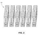
- FIG. 2shows a perspective view of cell-width strips 200 of thin film solar cell stacks.
- Substrate 211supports thin films 210 , 209 , 208 and 207 .
- Layers 208 and 209form a p-n junction, with a p-type semiconductor layer 209 deposited on a back electrical contact layer 210 and an n-type semiconductor layer 208 deposited on p-type semiconductor layer 209 to complete a p-n junction.
- any suitable semiconductor materialssuch as CIGS, CIS, CdTe, CdS, ZnS, ZnO, amorphous silicon, polycrystalline silicon, etc. are used for layers 208 and 209 .
- the p-type semiconductor layer 209may be CIGS or CIS
- the n-type semiconductor layer 208may be CdS or a cadmium free material, such as ZnS, ZnO, etc.
- Top electrode layer 207overlays the p-n junction. It is transparent, allowing light to reach light absorbing layer 209 .
- top transparent electrode layer 207is a transparent conducting oxide (TCO), for example, zinc oxide, aluminum-doped zinc oxide (AZO), indium tin oxide (ITO) and gallium doped zinc oxide.
- TCOtransparent conducting oxide
- AZOaluminum-doped zinc oxide
- ITOindium tin oxide
- Back electrical contact layer 210provides electrical contact to allow electrical current to flow through the solar cell, and may be made of any appropriate material, e.g., molybdenum, niobium, copper, silver, etc.
- substrate 211is a metallic substrate, e.g., a thin stainless steel foil, though it may also be other metals including but not limited to, titanium, copper, aluminum, beryllium and the like.
- the substrate 211may be relatively thin, such as for example, less than or equal to about 2-10 mils, though suitable thicknesses may also be used. In many cases the substrate is thin enough to be flexible.
- the stacks 200 shown in FIG. 2are long cell width strips, which may be cut further to define individual cells as shown in FIG. 1 .
- the thin film solar cells stacks shown in FIG. 2are provided for context and not intended to be limiting.
- the wire current collectors and/or interconnects described hereinmay be used with other types of solar cells as well as in other fields.
- the wire assemblyincludes serpentine wire 113 and wire carrier or decals 115 and 117 .
- wire 113is configured as a current collector to collect current generated by the solar cell and as a solar cell interconnect to electrically connect the cell to another cell, for example, in a solar module.
- the wiremay be configured only as a current collector or only as an interconnect.
- Wire 113overlays conductive transparent top layer 107 , and collects current generated from the cell.
- Wire 113is typically a thin, highly conductive metal wire. Examples of wire metals include copper, aluminum, nickel, chrome or alloys thereof. In some embodiments, a nickel coated copper wire is used. The wire should be able to maintain the serpentine form shown without significant material strain. In certain embodiments wire having a gauge of 24 gauge-56 gauge, or in particular embodiments, 32 gauge-56 gauge, for example 40 gauge-50 gauge.
- Front decal 115overlays all or part of portion 119 . (Back decal 117 , which overlies portion 121 of wire 113 , is not shown in this view for clarity).
- Front decal 115is a transparent, insulating carrier for the conductive wire.
- decal materialsinclude thermoplastic materials such as poly(ethylene terephthalate) (PET), ionomer resins, e.g., SurlynTM, polyamide, polyetheretherketone (PEEK), or combinations of these. In certain embodiments, it may not be used.
- FIG. 3shows a section 300 of a serpentine wire according to embodiments of the invention.
- the term “serpentine”refers to a form having substantially uniformly spaced, substantially co-extensive and substantially parallel lengths of wire connected via substantially rounded end portions. Uniformly spaced, co-extensive, parallel lengths 301 connected by rounded end portions 303 are indicated in FIG. 3 .
- the apparatuses and methods described hereinmay also be used to form wire current collectors having other configurations, e.g., such as angled zigzag patterns, etc.
- the pitch of the serpentine wiredetermines the distance current travels through the transparent conducting oxide prior to reaching the highly conductive wire. As shown in FIG. 3 , the maximum distance current has to travel through the transparent conductive oxide is 1 ⁇ 4 pitch. Reducing the pitch increases current collection, however, it also decreases the useful surface area of the cell. In certain embodiments, the pitch is between about 4 and 10 mm, e.g., about 6.5 mm, though other distances may also be used as appropriate.
- view 103depicts metallic substrate 111 and interconnect portion 121 of serpentine wire 113 .
- Back decal 117which overlies portion 121 of serpentine wire 113 as shown in view 103 , is an insulating carrier for serpentine wire 113 .
- the conductive side of interconnect portion 121faces down, able to make contact with a metallic substrate of an adjacent cell.
- FIG. 4shows the backsides of cells 410 a and 410 b including metallic substrates 411 a and 411 b .
- Wired interconnect 421 b of cell 410 boverlies metallic substrate 411 a of cell 410 a , thereby electrically connecting the cells 410 a and 410 b.
- the serpentine wireis provided on an insulating carrier, such as front and back decals described with reference to FIG. 1 .
- FIG. 5depicts front and back views of a strip of a wire assembly including serpentine wire 513 and front and back decals 515 and 517 , respectively.
- Front view 501shows serpentine wire 513 and front decal 515 , which overlies a portion of wire 513 .
- Back decal 517is not depicted in view 501 for clarity.
- Exposed portion 521 of wireinterconnects the cell as depicted in FIG. 4 .
- Back view 503shows serpentine wire 513 and back decal 517 , which overlies a portion of wire 513 .
- Exposed portion 519 of wire 513faces the top conducting oxide and acts as a current collector.
- a wire assemblyis affixed to the front side of a cell or cell width strip (such as those shown in FIG. 2 ).
- one or more of the decalsdo not overlie the rounded end portions of the serpentine wire.
- Embodiments of the inventionprovide apparatuses and methods of fabricating a wire assembly, including a serpentine wire and insulating carrier, such as that shown in FIG. 5 .
- the apparatusesinclude re-circulating chain link assemblies having uniformly pitched posts and a wire weaving assembly configured to weave wire around the posts as they circulate.
- the re-circulating chain link assembliesare disposed on opposite sides of a linear channel, with linear segments of each re-circulating chain path lining the channel. After being formed, the serpentine wire travels in the channel, where one or more decals may be applied.
- FIG. 6is a simplified schematic diagram depicting certain components of such an apparatus according to certain embodiments. Two chains 601 are disposed on opposite sides of a linear channel 605 .
- Linear guide 606is a raised surface within the channel 605 and provides guide channels 608 for chains 601 to feed through.
- Sprockets 607drive each chain through a path including a substantially linear segment aligning the channel 605 .
- Each chainre-circulates over its path in a direction indicated by the arrows.
- Re-circulating chains 601include links having vertically oriented posts (not shown) extending therefrom, around which a wire is woven to fabricate a serpentine wire. Once woven, the wire is guided via guide 606 through channel 605 before coming off the chain.
- At least one insulating carrieris applied to the serpentine wire prior to the wire coming off the chain.
- FIG. 6indicates approximate locations of certain operations along the linear channel 605 .
- a wireis woven around vertically oriented post members of the moving chains to form a serpentine wire as described above.
- the serpentine wiremoves down the linear channel 605 engaged on the posts of the chains.
- a first decalis applied at 612 .
- front and back decalsmay be applied.
- the decalis typically applied to overlie the serpentine wire as it is guided down the channel.
- the wire assemblyincluding the serpentine wire and decal carrier comes off the chains.
- a second decalis then applied to the serpentine wire, fabricating a wire assembly including front and back insulating carriers and serpentine wire as described above with respect to FIG. 5 .
- the chainscontinue to circulate, picking up newly woven wire at position 610 .
- the chains and postsmove at substantially constant rates.
- the re-circulating chainsinclude vertically-oriented posts extending from the chain links, around which the wire is woven.
- the pitch of the postsis uniform and corresponds to the pitch of the serpentine wire.
- the postsmay extend from the sides of the link bodies, extend from the top surface of the link bodies, etc.
- FIG. 7provides examples of multi-link chain segments, including vertically-oriented posts.
- Top down view 701shows an example of links 709 having uniformly spaced posts 711 extending from side surfaces of the links 709 ; and top down view 703 shows an example of links 709 with uniformly spaced posts 711 extending from the top surfaces of the links 709 .
- the postsare uniformly spaced across the entire chain; in certain embodiments, the number of posts extending from each link may vary.
- An exampleis shown in view 705 , in which links 709 have four posts and link 710 three posts. Link shape and size may vary as well to maintain uniform post spacing.
- the chainmay include a first set of links that engage with the sprockets and a set of adapter links disposed on the first set of links.
- Side view 707shows a set 713 of adapter links, including posts 711 , disposed on a set 715 of links.
- the vertically-oriented postsare uniformly sized and positioned with respect to the posts on the opposing chain to form the substantially parallel lengths and corresponding rounded end portions of the serpentine wire as depicted in FIG. 3 .
- Post diametercorresponds to the end rounded region diameter of the serpentine wire. According to various embodiments, the post diameter ranges from about 2.5 mm to 4 mm though other post sizes may be used as appropriate. In certain embodiments in which a serpentine form is fabricated, post diameter sets the pitch.
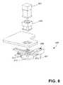
- FIG. 8depicts an exploded view of components of a wire weaving apparatus according to certain embodiments, including motor 801 , gear box 803 and weaving assembly 805 .
- Weaving assembly 805includes a tip 807 , to which wire is fed via feed 809 .
- Cam 813imparts simultaneous side-to-side motion (across the linear channel) to tip 807 via crank 815 , and back-and-forth motion (along the linear channel) via cam follower 817 .
- Back-and-forth motion as described aboveis also referred herein to as axial motion (i.e., along the direction of the axis of the linear channel), with side-to-side motion referred to as transverse motion (i.e., across the linear channel). Further details of these and other components of the weaving apparatus are described below with reference to FIGS. 10A and 10B .
- wireis fed through the wire weaver tip, which weaves around the posts of opposite re-circulating chains to form the serpentine wire.
- the movementcan be characterized as an elongated FIG. 8 motion.
- the exact form of the FIG. 8 motionmay be varied on a number of factors, including the alignment of posts on opposite re-circulating chains, i.e., the degree to which posts on a re-circulating chain are aligned or staggered with respect to posts on the opposing chain; the pitch of the serpentine wire; and the speeds of the chains as they move past the weaving apparatus.
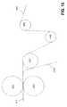
- FIG. 9depicts two not-to-scale examples 901 and 903 of a repeating path 909 of a wire weaver tip through posts 911 of opposing re-circulating chains.
- Path 909 of view 903is a symmetrical elongated FIG. 8 , path 909 of view 901 a slightly skewed FIG. 8 .
- the motion around the postsis exaggerated; in certain embodiments, the post clearances distances may be much tighter than depicted.
- the aspect ratio of the elongated FIG. 8 formed by the wire weaveris at least about 5:1; at least about 10:1; or at least about 15:1.
- the transverse distanceis about 53 mm, for posts 50 mm apart, with the axial distance being on the order of about 3.25 mm.
- the wire weaving apparatusis capable of weaving wire around the moving posts with tolerances of less than 1 or 0.1 mm. While the path may vary depending on the factors described above, however, the resulting wire dispensed by the tip is a serpentine form.
- FIG. 9also depicts a segment 905 formed by two FIG. 8 cycles. The axial distance is shown as “X” and the transverse distance as “Y.” In certain embodiments, X is about 3.25 mm and Y about 52.9 mm. As indicated, the actual distance traveled by the wire weaver may be slightly greater in certain embodiments to allow the wire tip to clear the posts.
- FIG. 10Adepicts a perspective view of weaving assembly 1000 and FIG. 10B a bottom view of weaving assembly 1000 .
- Various componentsincluding tip 1013 , tube 1014 , pen mount block 1010 , cam 1023 , crank 1009 , bearing 1006 , transverse rail mount 1004 , transverse rail 1007 , cam follower 1012 , spring mounts 1021 , springs 1026 , bearing 1031 , axial rail 1005 , and plate 1008 are depicted.
- a wireis fed to tip 1013 from a spool (not shown) via hollow tube 1014 .
- the tipmay be made of nylon in certain embodiments.
- a dancer roller or other wire tension control systemas known in the art may be employed to control the tension of the wire as it is fed to tip 1013 . Examples of dancer rollers are described in European Patent Publication 0114365 and U.S. Pat. Nos. 4,398,677 and 4,923,113.
- a motor(not shown) rotates cam 1023 via shaft 1024 .
- Cam 1023drives simultaneous transverse (side-to-side) and axial (back-and-forth) motions of pen mount block 1010 , and tube 1013 and tip 1014 mounted on block 1010 , to form an elongated FIG. 8 path described in FIG. 9 .
- crank 1009drives transverse motion of pen mount block 1010 .
- Bearing 1006is mounted on pen mount block 1010 allowing block 1010 to slide along transverse rail 1007 mounted on mount 1004 .
- pen mount block 1010slides side to side and back along rail 1010 one time.
- axial motionis imparted to plate 1008 and from plate 1008 to pen mount block 1010 via cam follower 1012 .
- the axial motionis dictated by the circumferential shape of cam 1023 , along which cam follower 1012 traces.
- Cam 1023deviates from a circular shape, with the deviations controlling the axial motion of pen mount block 1010 and tip 1013 .
- the required axial motionis relatively quick relative to the transverse motion as the tip 1013 goes around the outer edge of a post on one chain, and gradual as the tip traverses the desired width of the serpentine wire moving to a post on the opposite chain.
- cam 1023is shaped to provide two quick axial motions and two gradual axial motions during a single rotation. In operation, as cam 1023 rotates, cam follower 1012 mounted on plate 1008 follows the edge of cam 1023 .
- cam 1023has a continuously varying radius of curvature to provide continuous axial motion.
- the edge of cam 1023has two opposing rapid changes in curvature radius, separated by segments having gradual changes in curvature radius.
- cam 1023is an irregular oval shape.
- FIG. 11depicts an oval cam edge 1100 having irregular segments 1105 each with a rapid change in radius and that are separated by segments 1103 each having a gradual change in radius. While the cam shape is described generally here, one of skill in the art will understand that the precise shape may be irregular and vary depending on a number of factors including desired wire dispensing tip path, spring tension, etc.
- FIG. 12depicts a linear guide 1206 divided into two segments 1206 a and 1206 b .
- Segment 1206 aincludes left guide channel 1207 a and right guide channel 1208 a to guide opposing chains (not shown);
- segment 1206 bincludes left guide channel 1207 b and right guide channel 1208 b to guide opposing chains.
- wireis wound around posts of opposing chains at an approximate position 1210 to form the serpentine wire, which then travels down the linear channel on links of opposing chains to a position 1214 where it comes off the links.
- the distance between left channel 1207 b and right channel 1208 b of guide segment 1206 bis slightly greater than that between left channel 1207 a and right channel 1208 a of guide segment 1206 a , so that as opposing links enter guide segment 1206 b from segment 1206 a , the tension on the wire from the link posts increases.
- the guide segmentsare configured such that distance between opposing posts is 52 mm in segment 1206 a and 53 mm in segment 1206 b .
- FIG. 12presents an example of a linear guide configured such that the distance between posts narrows; in other embodiments, three or more segments may be used or the channels may angle slightly to achieve narrowing.
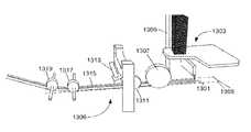
- FIG. 13shows a schematic illustrating decal application according to certain embodiments.
- Serpentine wire 1301is formed by weaving assembly 1303 as described above. For clarity, rounded end portions of serpentine wire 1301 are not shown.
- Opposing chainsare represented at 1305 , with individual links and posts not shown. After formation, serpentine wire travels down linear channel 1306 supported by moving chains 1305 .
- Rotating decal guide 1307lays thermoplastic decal strip 1309 from a spool (not shown) over serpentine wire 1301 .
- decal strip 1309does not overlie rounded end portions of serpentine wire 1301 , though in other embodiments it may.
- Roller 1311presses decal strip 1309 into serpentine wire as hot air jet (not shown) below the decal and wire heats the decal material, melting the thermoplastic thereby adhering decal strip 1309 to serpentine wire 1301 .
- Sensor 1313measures the temperature to ensure proper adhesion.
- Wire assembly 1315including decal strip 1309 and serpentine wire 1301 continue along linear channel 1306 , until pulled off chains 1305 by rollers (not shown).
- Rollers 1317 and 1319are positioned above the linear channel to modulate the angle at which the wire assembly 1315 is pulled off chains 1305 , allowing the wire assembly 1315 to come off chains 1305 gradually and without risking breakage.
- the posts of the linksare angled inwards to facilitate release off the serpentine wire and decal.
- FIG. 14depicts an example in which wire 1401 rides on chains 1405 through linear guide 1403 . (Chains are represented as 1405 ; for clarity, individual links and posts are not depicted. Each rounded end portion of serpentine wire 1401 is wrapped around a post of a chain 1405 . Also for clarity, center portion of guide 1403 and a decal are not depicted.)
- Two cylindrical members 1408are disposed at the end of linear guide 1403 on both sides of guide 1403 . As the links of the chains pass members 1408 , the links are angled inward away from the end portions of the formed serpentine wire 1401 .
- the serpentine wire 1401is then free to be lifted off the chains 1405 for further processing, while chains 1405 continue re-circulating as driven by sprockets 1407 .
- FIG. 15provides a schematic depiction of an apparatus configured for bottom decal application.
- Wire assembly 1501 including a serpentine wire and a top decalis depicted after release from the re-circulating posts as described in FIGS. 13 and 14 .
- Rollers 1503 , 1505 and 1507drive wire assembly 1501 towards hot lamination rollers 1513 .
- multiple rollers 1503 , 1505 and 1507are used to control wire assembly tension.
- bottom decal 1509is fed from a spool (not shown) to underlie wire assembly 1501 , positioned appropriately.
- the wire assembly 1501 and bottom decal 1509travel together between hot lamination rollers 1513 .
- the decalsare heated to a temperature of about 165° C. (+/ ⁇ 15° C.) and pressed together, forming wire and dual decal assembly 1511 .
- the wire assemblymay be complete and ready to be applied to solar cell thin films as described above.
- a non-serpentine uniformly-pitched wiremay be fabricated by appropriately adjusting the spacing and diameters of the posts. In this manner, for example, a wire having non-parallel segments connected by rounded ends may be formed. It should be noted that there are many alternative ways of implementing both the processes and apparatuses of the present invention. Accordingly, the present embodiments are to be considered as illustrative and not restrictive, and the invention is not to be limited to the details given herein.
Landscapes
- Woven Fabrics (AREA)
Abstract
Description
Claims (16)
Priority Applications (1)
| Application Number | Priority Date | Filing Date | Title |
|---|---|---|---|
| US12/687,754US8356640B1 (en) | 2010-01-14 | 2010-01-14 | Apparatuses and methods for fabricating wire current collectors and interconnects for solar cells |
Applications Claiming Priority (1)
| Application Number | Priority Date | Filing Date | Title |
|---|---|---|---|
| US12/687,754US8356640B1 (en) | 2010-01-14 | 2010-01-14 | Apparatuses and methods for fabricating wire current collectors and interconnects for solar cells |
Publications (1)
| Publication Number | Publication Date |
|---|---|
| US8356640B1true US8356640B1 (en) | 2013-01-22 |
Family
ID=47521650
Family Applications (1)
| Application Number | Title | Priority Date | Filing Date |
|---|---|---|---|
| US12/687,754Expired - Fee RelatedUS8356640B1 (en) | 2010-01-14 | 2010-01-14 | Apparatuses and methods for fabricating wire current collectors and interconnects for solar cells |
Country Status (1)
| Country | Link |
|---|---|
| US (1) | US8356640B1 (en) |
Cited By (11)
| Publication number | Priority date | Publication date | Assignee | Title |
|---|---|---|---|---|
| US20090235979A1 (en)* | 2008-03-20 | 2009-09-24 | Mulugeta Zerfu Wudu | Interconnect assembly |
| US20110197947A1 (en)* | 2008-03-20 | 2011-08-18 | Miasole | Wire network for interconnecting photovoltaic cells |
| US8951824B1 (en) | 2011-04-08 | 2015-02-10 | Apollo Precision (Fujian) Limited | Adhesives for attaching wire network to photovoltaic cells |
| US9061344B1 (en) | 2010-05-26 | 2015-06-23 | Apollo Precision (Fujian) Limited | Apparatuses and methods for fabricating wire current collectors and interconnects for solar cells |
| DE102014107454A1 (en) | 2014-05-27 | 2015-12-03 | Xenon Automatisierungstechnik Gmbh | Device for producing a busbar for contacting solar cells |
| US20160005940A1 (en)* | 2013-02-08 | 2016-01-07 | Osram Opto Semiconductors Gmbh | Device having at least one optoelectronic semiconductor component |
| US9620660B2 (en) | 2008-03-20 | 2017-04-11 | Beijing Apollo Ding Rong Solar Technology Co., Ltd. | Interconnect assembly |
| EP3198656A4 (en)* | 2014-10-31 | 2017-11-22 | BYD Company Limited | Solar cell module and manufacturing method thereof |
| US10026859B2 (en) | 2010-10-04 | 2018-07-17 | Beijing Apollo Ding Rong Solar Technology Co., Ltd. | Small gauge wire solar cell interconnect |
| US10381493B2 (en) | 2014-10-31 | 2019-08-13 | Byd Company Limited | Solar cell unit, solar cell array, solar cell module and manufacturing method thereof |
| CN111266484A (en)* | 2020-04-08 | 2020-06-12 | 昆山微容电子企业有限公司 | Bending device for manufacturing linear lead wire |
Citations (44)
| Publication number | Priority date | Publication date | Assignee | Title |
|---|---|---|---|---|
| US3459391A (en) | 1964-02-13 | 1969-08-05 | Nasa | Interconnection of solar cells |
| US3553030A (en) | 1967-11-15 | 1971-01-05 | Philips Corp | Radiation-sensitive semiconductor device |
| US3561500A (en)* | 1968-09-30 | 1971-02-09 | Gen Electric | Wire-forming apparatus and method |
| DE2757301A1 (en) | 1977-12-22 | 1979-07-05 | Leybold Heraeus Gmbh & Co Kg | Multiple element solar cell - has semiconductor elements enclosed between conductive and insulating layers with ends folded over and interlocked |
| US4560498A (en) | 1975-08-04 | 1985-12-24 | Raychem Corporation | Positive temperature coefficient of resistance compositions |
| US4694117A (en) | 1985-05-04 | 1987-09-15 | Telefunken Electronic Gmbh | Solar cell |
| US5034068A (en) | 1990-02-23 | 1991-07-23 | Spectrolab, Inc. | Photovoltaic cell having structurally supporting open conductive back electrode structure, and method of fabricating the cell |
| JPH0621501A (en) | 1992-03-31 | 1994-01-28 | Canon Inc | Solar cell module and method of manufacturing the same |
| US5330583A (en) | 1991-09-30 | 1994-07-19 | Sharp Kabushiki Kaisha | Solar battery module |
| US5391235A (en) | 1992-03-31 | 1995-02-21 | Canon Kabushiki Kaisha | Solar cell module and method of manufacturing the same |
| JPH0799334A (en) | 1993-08-06 | 1995-04-11 | Canon Inc | Photovoltaic device and module |
| JPH0936404A (en) | 1995-07-17 | 1997-02-07 | Canon Inc | Collector electrode, photovoltaic element, and method for manufacturing the same |
| US5620528A (en) | 1994-09-30 | 1997-04-15 | Siemens Solar Gmbh | Solar cell with a connecting structure |
| US5626688A (en) | 1994-12-01 | 1997-05-06 | Siemens Aktiengesellschaft | Solar cell with chalcopyrite absorber layer |
| JPH1093125A (en) | 1996-09-13 | 1998-04-10 | Sanyo Electric Co Ltd | Solar cell module |
| KR100242852B1 (en) | 1995-06-28 | 2000-02-01 | 미다라이 후지오 | Photovoltaic device and its manufacturing method |
| US6121542A (en) | 1996-05-17 | 2000-09-19 | Canon Kabushiki Kaisha | Photovoltaic device |
| US6132585A (en) | 1992-07-01 | 2000-10-17 | Canon Kabushiki Kaisha | Semiconductor element and method and apparatus for fabricating the same |
| US6184458B1 (en) | 1998-06-11 | 2001-02-06 | Canon Kabushiki Kaisha | Photovoltaic element and production method therefor |
| US6479744B1 (en) | 1997-12-22 | 2002-11-12 | Canon Kabushiki Kaisha | Photovoltaic device module |
| US20020166580A1 (en) | 2001-03-20 | 2002-11-14 | The Boeing Company | Method for fabricating a solar tile |
| US6531653B1 (en) | 2001-09-11 | 2003-03-11 | The Boeing Company | Low cost high solar flux photovoltaic concentrator receiver |
| US6600100B2 (en) | 1998-05-28 | 2003-07-29 | Emcore Corporation | Solar cell having an integral monolithically grown bypass diode |
| US20040069340A1 (en) | 1999-03-30 | 2004-04-15 | Daniel Luch | Substrate and collector grid structures for integrated series connected photovoltaic arrays and process of manufacture of such arrays |
| US20040187917A1 (en) | 2003-03-29 | 2004-09-30 | Nanosolar, Inc. | Transparent electrode, optoelectronic apparatus and devices |
| US20050072461A1 (en) | 2003-05-27 | 2005-04-07 | Frank Kuchinski | Pinhole porosity free insulating films on flexible metallic substrates for thin film applications |
| US20050176270A1 (en) | 2004-02-11 | 2005-08-11 | Daniel Luch | Methods and structures for the production of electrically treated items and electrical connections |
| JP2006041351A (en) | 2004-07-29 | 2006-02-09 | Canon Inc | Photovoltaic element manufacturing method |
| US20060180195A1 (en) | 1999-03-30 | 2006-08-17 | Daniel Luch | Substrate and collector grid structures for integrated photovoltaic arrays and process of manufacture of such arrays |
| US20070283997A1 (en) | 2006-06-13 | 2007-12-13 | Miasole | Photovoltaic module with integrated current collection and interconnection |
| EP1868250A2 (en) | 2006-06-13 | 2007-12-19 | Miasole | Photovoltaic module with integrated current collection and interconnection |
| US20080053511A1 (en) | 2004-04-28 | 2008-03-06 | Moritaka Nakamura | Integrated Wiring Member for Solar Cell Module, Solar Cell Module Using the Same, and Manufacturing Methods Thereof |
| US20080213477A1 (en) | 2007-03-02 | 2008-09-04 | Arno Zindel | Inline vacuum processing apparatus and method for processing substrates therein |
| US20080314433A1 (en) | 1995-05-15 | 2008-12-25 | Daniel Luch | Substrate structures for integrated series connected photovoltaic arrays and process of manufacture of such arrays |
| US7544884B2 (en) | 2002-09-30 | 2009-06-09 | Miasole | Manufacturing method for large-scale production of thin-film solar cells |
| US20090199894A1 (en) | 2007-12-14 | 2009-08-13 | Miasole | Photovoltaic devices protected from environment |
| CA2718518A1 (en) | 2008-03-20 | 2009-09-24 | Miasole | Interconnect assembly |
| US20100043863A1 (en) | 2008-03-20 | 2010-02-25 | Miasole | Interconnect assembly |
| US20100108122A1 (en) | 2008-11-04 | 2010-05-06 | Shawn Everson | Combined diode, lead assembly incorporating an expansion joint |
| US20100122730A1 (en) | 2008-11-17 | 2010-05-20 | Corneille Jason S | Power-loss-inhibiting current-collector |
| US20100212733A1 (en) | 2009-02-20 | 2010-08-26 | Miasole | Protective layer for large-scale production of thin-film solar cells |
| US20110197947A1 (en) | 2008-03-20 | 2011-08-18 | Miasole | Wire network for interconnecting photovoltaic cells |
| US20120080079A1 (en) | 2010-10-04 | 2012-04-05 | Miasole | Small gauge wire solar cell interconnect |
| US20120138117A1 (en) | 2008-03-20 | 2012-06-07 | Miasole | Thermoplastic wire network support for photovoltaic cells |
- 2010
- 2010-01-14USUS12/687,754patent/US8356640B1/ennot_activeExpired - Fee Related
Patent Citations (47)
| Publication number | Priority date | Publication date | Assignee | Title |
|---|---|---|---|---|
| US3459391A (en) | 1964-02-13 | 1969-08-05 | Nasa | Interconnection of solar cells |
| US3553030A (en) | 1967-11-15 | 1971-01-05 | Philips Corp | Radiation-sensitive semiconductor device |
| US3561500A (en)* | 1968-09-30 | 1971-02-09 | Gen Electric | Wire-forming apparatus and method |
| US4560498A (en) | 1975-08-04 | 1985-12-24 | Raychem Corporation | Positive temperature coefficient of resistance compositions |
| DE2757301A1 (en) | 1977-12-22 | 1979-07-05 | Leybold Heraeus Gmbh & Co Kg | Multiple element solar cell - has semiconductor elements enclosed between conductive and insulating layers with ends folded over and interlocked |
| US4694117A (en) | 1985-05-04 | 1987-09-15 | Telefunken Electronic Gmbh | Solar cell |
| US5034068A (en) | 1990-02-23 | 1991-07-23 | Spectrolab, Inc. | Photovoltaic cell having structurally supporting open conductive back electrode structure, and method of fabricating the cell |
| US5330583A (en) | 1991-09-30 | 1994-07-19 | Sharp Kabushiki Kaisha | Solar battery module |
| JPH0621501A (en) | 1992-03-31 | 1994-01-28 | Canon Inc | Solar cell module and method of manufacturing the same |
| US5391235A (en) | 1992-03-31 | 1995-02-21 | Canon Kabushiki Kaisha | Solar cell module and method of manufacturing the same |
| US6132585A (en) | 1992-07-01 | 2000-10-17 | Canon Kabushiki Kaisha | Semiconductor element and method and apparatus for fabricating the same |
| JPH0799334A (en) | 1993-08-06 | 1995-04-11 | Canon Inc | Photovoltaic device and module |
| US5620528A (en) | 1994-09-30 | 1997-04-15 | Siemens Solar Gmbh | Solar cell with a connecting structure |
| US5626688A (en) | 1994-12-01 | 1997-05-06 | Siemens Aktiengesellschaft | Solar cell with chalcopyrite absorber layer |
| US20080314433A1 (en) | 1995-05-15 | 2008-12-25 | Daniel Luch | Substrate structures for integrated series connected photovoltaic arrays and process of manufacture of such arrays |
| KR100242852B1 (en) | 1995-06-28 | 2000-02-01 | 미다라이 후지오 | Photovoltaic device and its manufacturing method |
| JPH0936404A (en) | 1995-07-17 | 1997-02-07 | Canon Inc | Collector electrode, photovoltaic element, and method for manufacturing the same |
| US6121542A (en) | 1996-05-17 | 2000-09-19 | Canon Kabushiki Kaisha | Photovoltaic device |
| JPH1093125A (en) | 1996-09-13 | 1998-04-10 | Sanyo Electric Co Ltd | Solar cell module |
| US6479744B1 (en) | 1997-12-22 | 2002-11-12 | Canon Kabushiki Kaisha | Photovoltaic device module |
| US6600100B2 (en) | 1998-05-28 | 2003-07-29 | Emcore Corporation | Solar cell having an integral monolithically grown bypass diode |
| US6184458B1 (en) | 1998-06-11 | 2001-02-06 | Canon Kabushiki Kaisha | Photovoltaic element and production method therefor |
| US20040069340A1 (en) | 1999-03-30 | 2004-04-15 | Daniel Luch | Substrate and collector grid structures for integrated series connected photovoltaic arrays and process of manufacture of such arrays |
| US20060180195A1 (en) | 1999-03-30 | 2006-08-17 | Daniel Luch | Substrate and collector grid structures for integrated photovoltaic arrays and process of manufacture of such arrays |
| US20020166580A1 (en) | 2001-03-20 | 2002-11-14 | The Boeing Company | Method for fabricating a solar tile |
| US6531653B1 (en) | 2001-09-11 | 2003-03-11 | The Boeing Company | Low cost high solar flux photovoltaic concentrator receiver |
| US7544884B2 (en) | 2002-09-30 | 2009-06-09 | Miasole | Manufacturing method for large-scale production of thin-film solar cells |
| US20040187917A1 (en) | 2003-03-29 | 2004-09-30 | Nanosolar, Inc. | Transparent electrode, optoelectronic apparatus and devices |
| US20050072461A1 (en) | 2003-05-27 | 2005-04-07 | Frank Kuchinski | Pinhole porosity free insulating films on flexible metallic substrates for thin film applications |
| US20050176270A1 (en) | 2004-02-11 | 2005-08-11 | Daniel Luch | Methods and structures for the production of electrically treated items and electrical connections |
| US20060032752A1 (en) | 2004-02-11 | 2006-02-16 | Daniel Luch | Methods and structures for the production of electrically treated items and electrical connections |
| US20080053511A1 (en) | 2004-04-28 | 2008-03-06 | Moritaka Nakamura | Integrated Wiring Member for Solar Cell Module, Solar Cell Module Using the Same, and Manufacturing Methods Thereof |
| JP2006041351A (en) | 2004-07-29 | 2006-02-09 | Canon Inc | Photovoltaic element manufacturing method |
| EP1868250A2 (en) | 2006-06-13 | 2007-12-19 | Miasole | Photovoltaic module with integrated current collection and interconnection |
| US20070283997A1 (en) | 2006-06-13 | 2007-12-13 | Miasole | Photovoltaic module with integrated current collection and interconnection |
| US20080213477A1 (en) | 2007-03-02 | 2008-09-04 | Arno Zindel | Inline vacuum processing apparatus and method for processing substrates therein |
| US20090199894A1 (en) | 2007-12-14 | 2009-08-13 | Miasole | Photovoltaic devices protected from environment |
| CA2718518A1 (en) | 2008-03-20 | 2009-09-24 | Miasole | Interconnect assembly |
| US20090235979A1 (en) | 2008-03-20 | 2009-09-24 | Mulugeta Zerfu Wudu | Interconnect assembly |
| US20100043863A1 (en) | 2008-03-20 | 2010-02-25 | Miasole | Interconnect assembly |
| US20110197947A1 (en) | 2008-03-20 | 2011-08-18 | Miasole | Wire network for interconnecting photovoltaic cells |
| US20120138117A1 (en) | 2008-03-20 | 2012-06-07 | Miasole | Thermoplastic wire network support for photovoltaic cells |
| US20100108122A1 (en) | 2008-11-04 | 2010-05-06 | Shawn Everson | Combined diode, lead assembly incorporating an expansion joint |
| US20100122730A1 (en) | 2008-11-17 | 2010-05-20 | Corneille Jason S | Power-loss-inhibiting current-collector |
| WO2010056803A2 (en) | 2008-11-17 | 2010-05-20 | Miasole | Power-loss-inhibiting current-collector |
| US20100212733A1 (en) | 2009-02-20 | 2010-08-26 | Miasole | Protective layer for large-scale production of thin-film solar cells |
| US20120080079A1 (en) | 2010-10-04 | 2012-04-05 | Miasole | Small gauge wire solar cell interconnect |
Non-Patent Citations (29)
| Title |
|---|
| Richards et al., "Enhancing the efficiency of production CdS/CdTe PV modules by overcoming poor spectral response at short wavelengths via luminescence down-shifting," 2006 IEEE 4th World Conference on Photovoltaic Energy Conversion, May 7-12, 2006, 4 pages. |
| U.S. Appl. No. 11/451,616, Office Action mailed Apr. 20, 2010. |
| U.S. Appl. No. 11/451,616, Office Action mailed Sep. 17, 2009. |
| U.S. Appl. No. 12/052,476, "Interconnect assembly", Zerfu et al., filed Mar. 20, 2008. |
| U.S. Appl. No. 12/052,476, Notice of Allowance mailed Jul. 18, 2012. |
| U.S. Appl. No. 12/052,476, Office Action mailed Aug. 3, 2011. |
| U.S. Appl. No. 12/052,476, Office Action mailed Jan. 21, 2011. |
| U.S. Appl. No. 12/052,476, Office Action mailed Mar. 16, 2012. |
| U.S. Appl. No. 12/272,600, "Power-loss-inhibiting current-collector", Corneille et al., filed Nov. 17, 2008. |
| U.S. Appl. No. 12/272,600, Office Action mailed Apr. 14, 2011. |
| U.S. Appl. No. 12/272,600, Office Action mailed Oct. 18, 2011. |
| U.S. Appl. No. 12/566,555, "Interconnect Assembly", Wudu et al., filed Sep. 24, 2009. |
| U.S. Appl. No. 12/566,555, Office Action mailed Feb. 16, 2012. |
| U.S. Appl. No. 12/819,124, "Power-loss-inhibiting current collector having transparent current regulator", Corneille et al., filed Jun. 18, 2010. |
| U.S. Appl. No. 12/837,867, "Transparent conductive film-coated decals for solar cells", Corneille et al., filed Jul. 16, 2010. |
| U.S. Appl. No. 12/843,648, "Temperature resistant current collectors for thin film photovoltaic cells", Alex Austin, filed Jul. 26, 2010. |
| U.S. Appl. No. 12/897,162, "Small gauge wire solar cell interconnect", Corneille et al., filed Oct. 4, 2010. |
| U.S. Appl. No. 12/915,882, "Apparatus and method for securing wire to decal", McKay et al., filed Oct. 29, 2010. |
| U.S. Appl. No. 12/915,882, Office Action mailed Jul. 20, 2012. |
| U.S. Appl. No. 12/951,711, "Photovoltaic Device and Method and System for Making Photovoltaic Device," Austen, filed Nov. 22, 2010. |
| U.S. Appl. No. 13/082,709, "Adhesives for attaching wire network to photovoltaic cells", Todd Krajewski, filed Apr. 8, 2011. |
| U.S. Appl. No. 13/085,274, "Thermoplastic wire network support for photovoltaic cells", Todd Krajewski, filed Apr. 12, 2011. |
| U.S. Appl. No. 13/087,724, "Wire network for interconnecting photovoltaic cells", Steven Croft, filed Apr. 15, 2011. |
| U.S. Appl. No. 13/087,730, "Interconnecting wire network with conductive tab", Steven Croft, filed Apr. 15, 2011. |
| U.S. Appl. No. 13/114,999, "Apparatuses and methods for fabricating wire current collectors and interconnects for solar cells", McKay et al., filed May 24, 2011. |
| U.S. Appl. No. 13/114,999, "Apparatuses and Methods for Fabricating wire Current Collectors and Interconnects for Solar Cells," McKay et al., filed May 24, 2011. |
| U.S. Appl. No. PCT/US2009/064125, International Search Report and Written Opinion, mailed May 24, 2010. |
| Untila et al., "19.2% Efficient Bifacial ITO-(P+Nn+)Si-ITO Laminated Grid Cell, 16th European Photovoltaic Solar Energy Conference," May 1-5, 2000, Glasgow, UK, pp. 1489-1491. |
| WO patent application No. PCT/US2009/035486, International Search Report and Written Opinion, mailed Sep. 29, 2009. |
Cited By (16)
| Publication number | Priority date | Publication date | Assignee | Title |
|---|---|---|---|---|
| US9620660B2 (en) | 2008-03-20 | 2017-04-11 | Beijing Apollo Ding Rong Solar Technology Co., Ltd. | Interconnect assembly |
| US20110197947A1 (en)* | 2008-03-20 | 2011-08-18 | Miasole | Wire network for interconnecting photovoltaic cells |
| US10056521B2 (en) | 2008-03-20 | 2018-08-21 | Beijing Apollo Ding Rong Solar Technology Co., Ltd. | Wire network for interconnecting photovoltaic cells |
| US20090235979A1 (en)* | 2008-03-20 | 2009-09-24 | Mulugeta Zerfu Wudu | Interconnect assembly |
| US9061344B1 (en) | 2010-05-26 | 2015-06-23 | Apollo Precision (Fujian) Limited | Apparatuses and methods for fabricating wire current collectors and interconnects for solar cells |
| US10026859B2 (en) | 2010-10-04 | 2018-07-17 | Beijing Apollo Ding Rong Solar Technology Co., Ltd. | Small gauge wire solar cell interconnect |
| US9647160B2 (en) | 2011-04-08 | 2017-05-09 | Beijing Apollo Ding Rong Solar Technology Co., Ltd. | Adhesives for attaching wire network to photovoltaic cells |
| US8951824B1 (en) | 2011-04-08 | 2015-02-10 | Apollo Precision (Fujian) Limited | Adhesives for attaching wire network to photovoltaic cells |
| US20160005940A1 (en)* | 2013-02-08 | 2016-01-07 | Osram Opto Semiconductors Gmbh | Device having at least one optoelectronic semiconductor component |
| US9972759B2 (en)* | 2013-02-08 | 2018-05-15 | Osram Opto Semiconductors Gmbh | Optoelectronic semiconductor device having contact track with relieved thermo-mechanical stress |
| DE102014107454B4 (en)* | 2014-05-27 | 2016-05-19 | Xenon Automatisierungstechnik Gmbh | Device for producing a busbar for contacting solar cells |
| DE102014107454A1 (en) | 2014-05-27 | 2015-12-03 | Xenon Automatisierungstechnik Gmbh | Device for producing a busbar for contacting solar cells |
| EP3198656A4 (en)* | 2014-10-31 | 2017-11-22 | BYD Company Limited | Solar cell module and manufacturing method thereof |
| US10381493B2 (en) | 2014-10-31 | 2019-08-13 | Byd Company Limited | Solar cell unit, solar cell array, solar cell module and manufacturing method thereof |
| US10529868B2 (en) | 2014-10-31 | 2020-01-07 | Byd Company Limited | Solar cell array, solar cell module and manufacturing method thereof |
| CN111266484A (en)* | 2020-04-08 | 2020-06-12 | 昆山微容电子企业有限公司 | Bending device for manufacturing linear lead wire |
Similar Documents
| Publication | Publication Date | Title |
|---|---|---|
| US8356640B1 (en) | Apparatuses and methods for fabricating wire current collectors and interconnects for solar cells | |
| US20190181294A1 (en) | Wire network for interconnecting photovoltaic cells | |
| US9065008B2 (en) | Automated assembly method for the production of interconnected thin film solar cell modules | |
| US10026859B2 (en) | Small gauge wire solar cell interconnect | |
| US9601651B2 (en) | Method and apparatus for manufacturing a solar module strand and a solar module strand of flexible solar cells | |
| EP3171412B1 (en) | Apparatus and method for attaching interconnector of solar cell panel | |
| US20120294967A1 (en) | Machine for Manufacturing Electrode Tape | |
| US20140060615A1 (en) | Method and device for connecting solar cells to form a solar cell string, and a solar cell string | |
| EP2348538A2 (en) | Solar cell and method for manufacturing the same | |
| US9061344B1 (en) | Apparatuses and methods for fabricating wire current collectors and interconnects for solar cells | |
| EP3157065B1 (en) | Apparatus and method for attaching interconnector of solar cell panel | |
| CN110165004A (en) | Photovoltaic power generation and storage equipment and its manufacturing method | |
| EP3051595A1 (en) | Method and device for making an interconnector for solar cells and such interconnector | |
| EP4425579A1 (en) | Method of manufacturing solar cell string | |
| EP3944342B1 (en) | Method for interconnecting photovoltaic cells and photovoltaic cells assembly being producible thereby | |
| US9391219B2 (en) | Photovoltaic apparatus | |
| WO2011011348A2 (en) | Method of manufacturing a photovoltaic device | |
| KR102024083B1 (en) | Solar cell panel, and apparatus and method for attaching interconnector of solar cell panel | |
| CN104810413B (en) | Solar battery front side contact layer with thickness gradient | |
| US20250113645A1 (en) | An apparatus for manufacturing an electrode assembly | |
| KR101325141B1 (en) | Apparatus and method for processing of material | |
| KR101425930B1 (en) | Manufacturing method for photovoltaic ribbon reduced plating solution and the photovoltaic ribbon | |
| US20110253189A1 (en) | Thin-film solar cell | |
| WO2025119870A1 (en) | An electrode assembly and a method of manufacturing an electrode assembly | |
| EP2874189A2 (en) | Scribing apparatus for manufacturing solar cells |
Legal Events
| Date | Code | Title | Description |
|---|---|---|---|
| AS | Assignment | Owner name:MIASOLE, CALIFORNIA Free format text:ASSIGNMENT OF ASSIGNORS INTEREST;ASSIGNORS:NIZENKOFF, ERIK;ZEVENBERGEN, JOHN;BIRTWHISTLE, DARIN;AND OTHERS;REEL/FRAME:023795/0157 Effective date:20100111 | |
| AS | Assignment | Owner name:PINNACLE VENTURES, L.L.C., CALIFORNIA Free format text:SECURITY AGREEMENT;ASSIGNOR:MIASOLE;REEL/FRAME:028863/0887 Effective date:20120828 | |
| STCF | Information on status: patent grant | Free format text:PATENTED CASE | |
| AS | Assignment | Owner name:MIASOLE, CALIFORNIA Free format text:RELEASE BY SECURED PARTY;ASSIGNOR:PINNACLE VENTURES, L.L.C.;REEL/FRAME:029579/0494 Effective date:20130107 | |
| AS | Assignment | Owner name:HANERGY HOLDING GROUP LTD, CHINA Free format text:CONFIRMATORY ASSIGNMENT OF PATENT RIGHTS;ASSIGNOR:MIASOLE;REEL/FRAME:032127/0428 Effective date:20140109 | |
| FEPP | Fee payment procedure | Free format text:PAT HOLDER NO LONGER CLAIMS SMALL ENTITY STATUS, ENTITY STATUS SET TO UNDISCOUNTED (ORIGINAL EVENT CODE: STOL); ENTITY STATUS OF PATENT OWNER: LARGE ENTITY | |
| AS | Assignment | Owner name:APOLLO PRECISION (KUNMING) YUANHONG LIMITED, CHINA Free format text:ASSIGNMENT OF ASSIGNORS INTEREST;ASSIGNOR:HANERGY HOLDING GROUP LTD.;REEL/FRAME:034857/0380 Effective date:20140810 | |
| AS | Assignment | Owner name:BEIJING APOLLO DING RONG SOLAR TECHNOLOGY CO., LTD Free format text:ASSIGNMENT OF ASSIGNORS INTEREST;ASSIGNOR:APOLLO PRECISION (KUNMING) YUANHONG LIMITED;REEL/FRAME:037896/0010 Effective date:20160225 | |
| REMI | Maintenance fee reminder mailed | ||
| FPAY | Fee payment | Year of fee payment:4 | |
| SULP | Surcharge for late payment | ||
| MAFP | Maintenance fee payment | Free format text:PAYMENT OF MAINTENANCE FEE, 8TH YEAR, LARGE ENTITY (ORIGINAL EVENT CODE: M1552); ENTITY STATUS OF PATENT OWNER: LARGE ENTITY Year of fee payment:8 | |
| FEPP | Fee payment procedure | Free format text:MAINTENANCE FEE REMINDER MAILED (ORIGINAL EVENT CODE: REM.); ENTITY STATUS OF PATENT OWNER: LARGE ENTITY | |
| LAPS | Lapse for failure to pay maintenance fees | Free format text:PATENT EXPIRED FOR FAILURE TO PAY MAINTENANCE FEES (ORIGINAL EVENT CODE: EXP.); ENTITY STATUS OF PATENT OWNER: LARGE ENTITY | |
| STCH | Information on status: patent discontinuation | Free format text:PATENT EXPIRED DUE TO NONPAYMENT OF MAINTENANCE FEES UNDER 37 CFR 1.362 | |
| FP | Lapsed due to failure to pay maintenance fee | Effective date:20250122 |