US8351239B2 - Dynamic sense current supply circuit and associated method for reading and characterizing a resistive memory array - Google Patents
Dynamic sense current supply circuit and associated method for reading and characterizing a resistive memory arrayDownload PDFInfo
- Publication number
- US8351239B2 US8351239B2US12/604,915US60491509AUS8351239B2US 8351239 B2US8351239 B2US 8351239B2US 60491509 AUS60491509 AUS 60491509AUS 8351239 B2US8351239 B2US 8351239B2
- Authority
- US
- United States
- Prior art keywords
- circuit
- current
- current mirror
- mirror sub
- stage
- Prior art date
- Legal status (The legal status is an assumption and is not a legal conclusion. Google has not performed a legal analysis and makes no representation as to the accuracy of the status listed.)
- Active, expires
Links
Images


Classifications
- G—PHYSICS
- G11—INFORMATION STORAGE
- G11C—STATIC STORES
- G11C7/00—Arrangements for writing information into, or reading information out from, a digital store
- G11C7/10—Input/output [I/O] data interface arrangements, e.g. I/O data control circuits, I/O data buffers
- G11C7/1015—Read-write modes for single port memories, i.e. having either a random port or a serial port
- G11C7/1045—Read-write mode select circuits
- G—PHYSICS
- G11—INFORMATION STORAGE
- G11C—STATIC STORES
- G11C11/00—Digital stores characterised by the use of particular electric or magnetic storage elements; Storage elements therefor
- G11C11/56—Digital stores characterised by the use of particular electric or magnetic storage elements; Storage elements therefor using storage elements with more than two stable states represented by steps, e.g. of voltage, current, phase, frequency
- G11C11/5678—Digital stores characterised by the use of particular electric or magnetic storage elements; Storage elements therefor using storage elements with more than two stable states represented by steps, e.g. of voltage, current, phase, frequency using amorphous/crystalline phase transition storage elements
- G—PHYSICS
- G11—INFORMATION STORAGE
- G11C—STATIC STORES
- G11C11/00—Digital stores characterised by the use of particular electric or magnetic storage elements; Storage elements therefor
- G11C11/56—Digital stores characterised by the use of particular electric or magnetic storage elements; Storage elements therefor using storage elements with more than two stable states represented by steps, e.g. of voltage, current, phase, frequency
- G11C11/5685—Digital stores characterised by the use of particular electric or magnetic storage elements; Storage elements therefor using storage elements with more than two stable states represented by steps, e.g. of voltage, current, phase, frequency using storage elements comprising metal oxide memory material, e.g. perovskites
- G—PHYSICS
- G11—INFORMATION STORAGE
- G11C—STATIC STORES
- G11C13/00—Digital stores characterised by the use of storage elements not covered by groups G11C11/00, G11C23/00, or G11C25/00
- G11C13/0002—Digital stores characterised by the use of storage elements not covered by groups G11C11/00, G11C23/00, or G11C25/00 using resistive RAM [RRAM] elements
- G11C13/0004—Digital stores characterised by the use of storage elements not covered by groups G11C11/00, G11C23/00, or G11C25/00 using resistive RAM [RRAM] elements comprising amorphous/crystalline phase transition cells
- G—PHYSICS
- G11—INFORMATION STORAGE
- G11C—STATIC STORES
- G11C13/00—Digital stores characterised by the use of storage elements not covered by groups G11C11/00, G11C23/00, or G11C25/00
- G11C13/0002—Digital stores characterised by the use of storage elements not covered by groups G11C11/00, G11C23/00, or G11C25/00 using resistive RAM [RRAM] elements
- G11C13/0007—Digital stores characterised by the use of storage elements not covered by groups G11C11/00, G11C23/00, or G11C25/00 using resistive RAM [RRAM] elements comprising metal oxide memory material, e.g. perovskites
- G—PHYSICS
- G11—INFORMATION STORAGE
- G11C—STATIC STORES
- G11C13/00—Digital stores characterised by the use of storage elements not covered by groups G11C11/00, G11C23/00, or G11C25/00
- G11C13/0002—Digital stores characterised by the use of storage elements not covered by groups G11C11/00, G11C23/00, or G11C25/00 using resistive RAM [RRAM] elements
- G11C13/0021—Auxiliary circuits
- G11C13/004—Reading or sensing circuits or methods
- G—PHYSICS
- G11—INFORMATION STORAGE
- G11C—STATIC STORES
- G11C29/00—Checking stores for correct operation ; Subsequent repair; Testing stores during standby or offline operation
- G11C29/02—Detection or location of defective auxiliary circuits, e.g. defective refresh counters
- G—PHYSICS
- G11—INFORMATION STORAGE
- G11C—STATIC STORES
- G11C29/00—Checking stores for correct operation ; Subsequent repair; Testing stores during standby or offline operation
- G11C29/02—Detection or location of defective auxiliary circuits, e.g. defective refresh counters
- G11C29/026—Detection or location of defective auxiliary circuits, e.g. defective refresh counters in sense amplifiers
- G—PHYSICS
- G11—INFORMATION STORAGE
- G11C—STATIC STORES
- G11C29/00—Checking stores for correct operation ; Subsequent repair; Testing stores during standby or offline operation
- G11C29/04—Detection or location of defective memory elements, e.g. cell constructio details, timing of test signals
- G11C29/50—Marginal testing, e.g. race, voltage or current testing
- G—PHYSICS
- G11—INFORMATION STORAGE
- G11C—STATIC STORES
- G11C7/00—Arrangements for writing information into, or reading information out from, a digital store
- G11C7/14—Dummy cell management; Sense reference voltage generators
- G—PHYSICS
- G11—INFORMATION STORAGE
- G11C—STATIC STORES
- G11C13/00—Digital stores characterised by the use of storage elements not covered by groups G11C11/00, G11C23/00, or G11C25/00
- G11C13/0002—Digital stores characterised by the use of storage elements not covered by groups G11C11/00, G11C23/00, or G11C25/00 using resistive RAM [RRAM] elements
- G11C13/0021—Auxiliary circuits
- G11C13/004—Reading or sensing circuits or methods
- G11C2013/0045—Read using current through the cell
- G—PHYSICS
- G11—INFORMATION STORAGE
- G11C—STATIC STORES
- G11C13/00—Digital stores characterised by the use of storage elements not covered by groups G11C11/00, G11C23/00, or G11C25/00
- G11C13/0002—Digital stores characterised by the use of storage elements not covered by groups G11C11/00, G11C23/00, or G11C25/00 using resistive RAM [RRAM] elements
- G11C13/0021—Auxiliary circuits
- G11C13/004—Reading or sensing circuits or methods
- G11C2013/0054—Read is performed on a reference element, e.g. cell, and the reference sensed value is used to compare the sensed value of the selected cell
- G—PHYSICS
- G11—INFORMATION STORAGE
- G11C—STATIC STORES
- G11C29/00—Checking stores for correct operation ; Subsequent repair; Testing stores during standby or offline operation
- G11C29/04—Detection or location of defective memory elements, e.g. cell constructio details, timing of test signals
- G11C29/50—Marginal testing, e.g. race, voltage or current testing
- G11C2029/5006—Current
- G—PHYSICS
- G11—INFORMATION STORAGE
- G11C—STATIC STORES
- G11C2211/00—Indexing scheme relating to digital stores characterized by the use of particular electric or magnetic storage elements; Storage elements therefor
- G11C2211/56—Indexing scheme relating to G11C11/56 and sub-groups for features not covered by these groups
- G11C2211/564—Miscellaneous aspects
- G11C2211/5645—Multilevel memory with current-mirror arrangements
Definitions
- Nonvolatile Nanotube Diodes and Nonvolatile Nanotube Blocks and Systems Using Same and Methods of Making Same(U.S. patent application Ser. No. 11/835,856), filed Aug. 8, 2007;
- Nonvolatile Resistive Memories having Scalable Two-Terminal Nanotube Switches(U.S. patent application Ser. No. 11/835,612), filed Aug. 8, 2007.
- the present applicationgenerally relates to memory arrays and more particularly to circuits and methods for sensing, reading, and characterizing memory arrays.
- Resistive memory arrayshave taken many forms.
- resistive memory arrayscan take the form of magneto-resistive memory arrays such as is disclosed in U.S. Pat. No. 6,999,340 to Shimizu.
- the memory cellscan be set to a plurality of non-volatile resistive states and thus can be used to encode digital information. For example, a high resistive state can be used to indicate a digital “1” (or high) and a low resistive state can be used to indicate a digital “0” (or low).
- a sense current(sometimes referred to as a “read current” by those skilled in the art) is applied to a memory cell and the resulting voltage used to determine the resistive state of the cell.
- a key parameter in resistive memory array circuitsis the device's responsiveness to a given range of sense currents.
- each cell within the memory arrayis written with a test value.
- Various electrical currentsare then supplied to each memory cell within the memory array, and the resulting voltages analyzed to determine if the expected value was successfully read by each of the plurality of applied sense currents. In this way, the effectiveness of different sense currents can be characterized for the entire memory array.
- U.S. Pat. No. 7,106,644 to Chouteaches an improved circuit and associated test method for performing a burn in test on a memory array.
- a plurality of current limiting circuitsare used to limit the current through each word line during the burn-in test, thus allowing a test voltage to sufficiently stress a plurality of word lines simultaneously.
- U.S. Pat. No. 6,704,233 to Conte et al.teaches a circuit and associated method for reading a memory cell within a memory array.
- the circuit of Conte et al.comprises a reference memory cell, a current supply, a pair of transimpedance amplifiers, and a comparator.
- Conte et al.generates and then passes a sense (read) current through both the memory cell under test and the reference memory cell, converting the currents through the memory cell under test and the reference memory cell to voltages (via the transimpedance amplifiers). Finally, the resulting voltages can be compared to obtain a digital representation of the bit stored in the memory cell under test.
- U.S. Pat. No. 5,926,422 to Hauknessteaches a circuit and associated method for rapidly testing a large memory array.
- a plurality of memory cellsare sensed by a circuit which reports a digital value (a “high” or a “low”) indicating if all of the bits stored within said plurality of memory cells are of the same value. That is, Haukness' method significantly reduces the time required to verify a memory array by verifying the data state of a plurality of individual memory cells simultaneously.
- an electronic circuit for characterizing a resistive memory arrayincludes a first current mirror sub-circuit, the first current mirror sub-circuit including a first stage and a second stage, the second stage including at least two current branches and wherein at least one of the current branches is responsive to an enable control.
- the circuitfurther includes a second current mirror sub-circuit, the second current mirror sub-circuit including a first stage and a second stage, the second stage including at least two current branches and wherein at least one of the current branches is responsive to an enable control.
- the circuitfurther includes an interconnection to couple a current generated within the first current mirror sub-circuit to the second current mirror sub-circuit.
- the circuitfurther includes a reference current terminal to apply an external reference current to the first current mirror sub-circuit.
- the circuitfurther includes a sense current terminal to apply a sense current generated through the second current mirror sub-circuit to a memory cell under test.
- the circuitfurther includes a digital circuit element to generate a digital signal indicative of a magnitude of a current flowing through at least one stage of the second current mirror sub-circuit.
- the present disclosurealso provides a method for characterizing a resistive memory array, the memory array including a plurality of memory cells.
- the methodincludes the steps of first electrically coupling a dynamic sense current supply circuit to a first memory cell within the memory array, then generating a first sense current through the dynamic sense current supply circuit to perform a read operation, then recording the result of the read operation, then repeating the steps of generating and recording for a predetermined range of sense currents, then electrically coupling to a second memory cell within the memory array and repeating the steps of generating and recording for a predetermined range of sense currents, and then further repeating the steps of electrically coupling, generating, and recording such that a desired plurality of memory cells within the resistive memory array are characterized.
- the dynamic sense current supply circuit of the present disclosureincludes two programmable current mirror circuits.
- Each of the programmable current mirror circuitsfurther includes a plurality of second stage branches responsive to external control signals. By selectively enabling and disabling the plurality of second stage branches, a dynamically controlled scaling factor is provided through each of the programmable current mirror circuits.
- the programmable current mirror circuitsare arranged to provide a scaled version of a “base” current—the “base” current supplied from a single current supply—to a resistive memory cell under test.
- a plurality of sense currentscan be realized and provided to the resistive memory cell under test without connecting and disconnecting various current supplies or mechanically switching various circuit elements in and out.
- a first programmable current mirroris used to provide a first scaling factor and a second programmable current mirror is used to provide a second scaling factor.
- the programmable current mirror circuitsare comprised of field effect transistors (FETs), the aspect ratios of which—that is, the ratio of the width of the gate to the length of the gate within the structure of the FET—are selected to provide desired scale factors through the programmable current mirror circuits.
- FETsfield effect transistors
- the dynamic sense current supply circuitfurther includes a method to sense the condition of a valid sense current through the circuit and provide a digital output signal representative of the condition.
- the dynamic sense current supply circuit of the present disclosureis used within a memory array characterization system.
- the systemprovides the sense currents generated within the dynamic sense current supply circuit to the plurality of individual memory cells within the memory array under test, allowing each of the individual memory cells to be rapidly tested with the plurality of sense currents provided by the dynamic sense current supply circuit.
- the circuitprovide a range of sense currents to a memory cell under test, the sense currents dynamically selectable via one or more digital control lines.
- the circuitprovide a digital output indicative of the state of the memory cell under test as read by the applied sense current.
- FIG. 1is a simplified schematic diagram depicting a dynamic sense current supply circuit according to one or more embodiments
- FIGS. 2A-2Care tables detailing the selection bit configuration settings for the dynamic sense current supply circuit of FIG. 1 , according to one or more embodiments of the present disclosure
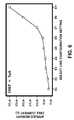
- FIG. 3is a plot graphically illustrating the range of sense currents available to the circuit of FIG. 1 using a base reference current of 5 ⁇ A, according to one or more embodiments of the present disclosure
- FIG. 4is a simplified schematic depicting a dynamic sense current supply circuit, according to one or more embodiments of the present disclosure
- FIGS. 5A-5Care tables detailing the selection bit configuration settings for the dynamic sense current supply circuit of FIG. 4 , according to one or more embodiments of the present disclosure
- FIG. 6is a plot graphically illustrating the sense currents available to the circuit of FIG. 4 using a base reference current of 5 ⁇ A, according to one or more embodiments of the present disclosure
- FIG. 7is a functional block diagram of a memory array characterization system using the circuit and methods of the present disclosure.
- FIG. 8is a flow chart detailing a memory array characterization operation using the methods of the present disclosure.
- the present disclosureprovides a method for rapidly characterizing an array of resistive memory elements.
- programmable current mirror circuitsare used to scale a supplied reference current and then provide this scaled current to a resistive memory cell under test.
- the programmable current mirror circuitscan include multiple branches which are responsive to external control signals. By enabling or disabling these current branches (through the use of these external control signals), the scaling factors through the programmable current mirror circuits can be dynamically set, allowing a plurality of different sense currents to be rapidly provided to the memory cell under test using a single source.
- the methods of the present inventioncan also be used to read a multi-level resistive memory element.
- Multi-level resistive memory elementscan store multiple bits of information in a single cell by providing more than two resistive states within that cell. For example, a resistive memory cell capable of storing four distinct resistive states would be capable of storing two binary bits of data (two bits corresponding to four distinct data values—bx00, bx01, bx10, and bx11).
- reading multi-level resistive memory cellsrequires that a plurality of sense currents be employed. As such, the methods of the present disclosure (as well as the associated circuits) are well suited to rapidly read the sate of such cells.
- FIG. 1is a simplified schematic diagram illustrating an exemplary dynamic sense current supply circuit for characterizing and reading a resistive memory cell under test under the methods of the present disclosure.
- the dynamic sense current supply circuit illustrated in FIG. 1has two subsections.
- a first programmable current mirror sub-circuit 110is electrically interposed between a reference node 170 and a digital output node 190 .
- a second mirror sub-circuit 120is electrically interposed between the memory cell under test 140 and the digital output node 190 .
- the first programmable current mirror sub-circuit 110provides scaling factor A to reference current I 1 , resulting in intermediate current I 2 .
- the second programmable current mirror sub-circuit 120provides scaling factor 1/B to intermediate current I 2 , resulting in sense current I 3 .
- scaling factorsare selected by enabling or disabling the different branches ( 110 a - 110 d and 120 a - 120 d ) within each programmable current mirror ( 110 and 120 , respectively). Operated together, they facilitate a dynamically programmable sense current for testing a resistive memory cell 140 .
- the first programmable current mirror sub-circuit 110includes a first stage—the first stage including FETs Q 101 and Q 102 —and a second stage.
- the second stagehas several branches 110 a , 110 b , 110 c , and 110 d .
- Each of these branchesincludes an enable FET (Q 103 , Q 105 , Q 107 , and Q 109 , respectively) and a main FET (Q 104 , Q 106 , Q 108 , and Q 110 , respectively).
- the gate of the enable FET Q 103 within the first branch 110 ais tied to ground, permanently enabling said first branch 110 a .
- the gates of the enable FETs (Q 105 , Q 107 , and Q 109 ) in the remaining branches ( 110 b , 110 c , and 110 d , respectively)are responsive to a first bank of digital control signals 150 (SEL 101 , SEL 102 , and SEL 103 , respectively).
- the first bank of digital control signals 150enable and disable the remaining branches ( 110 b , 110 c , and 110 d ) within the second stage of the programmable current mirror sub-circuit 110 .
- the gate aspect ratio(that is, the ratio of the width of the gate to the length of the gate within the structure of the FET) of the main FET within each of the different branches of the second stage (Q 104 , Q 106 , Q 108 , and Q 110 ) is substantially equal to the gate aspect ratio of the main FET within the first stage Q 102 .
- the gate aspect ratios of the main FET within each of the enabled brancheseffectively combine, creating a gate aspect ratio mismatch between the first and second stages of the programmable current mirror sub-circuit 110 .
- Such a mismatchprovides a scale factor (denoted as “A” within the simplified schematic diagram of FIG. 1 ) to a current passed through the first programmable current mirror sub-circuit 110 .
- a reference current supply 130provides a constant “base” current I 1 (equal to a current value of “IREF” within the simplified schematic diagram of FIG. 1 ) through the first stage of the programmable current mirror sub-circuit 110 (FETs Q 101 and Q 102 ). Responsive to this supplied “base” current, the programmable current mirror sub-circuit 110 provides a scaled version of I 1 through its second stage. This scaled current is denoted as I 2 and is substantially equal to the current value of “IREF” times the scale factor (“IREF*A”).
- this first scale factor (“A”)is directly proportional to the number of current branches enabled within—and thus the effective gate aspect ratio of—the second stage of the programmable current mirror sub-circuit 110 .
- FIG. 2Aprovides a table of nominal values of this first scale factor (“A”) for a plurality of control line 150 settings.
- a fixed current mirror circuit(that is, a non-programmable current mirror circuit) is used to interconnect the first and second current mirror sub-circuits 110 and 120 .
- the fixed current mirror circuit connectionhas two FETs, Q 111 and Q 112 and provides the scaled current I 2 to the second stage of a second programmable current mirror sub-circuit 120 .
- Second programmable current mirror sub-circuit 120is used to provide a second sense current scaling factor “B.”
- a second bank of digital control lines 160(SEL 104 , SEL 105 , and SEL 106 ) enable and disable a plurality of current branches ( 120 b , 120 c , and 120 d , respectively) within the second stage of the programmable current mirror sub-circuit 120 .
- enabling more than one of these current branchesintroduces an effective gate aspect ratio mismatch between the first stage (comprised of Q 113 and Q 114 ) and the second stage of the programmable current mirror sub-circuit 120 .
- Such a gate aspect ratio mismatcheffectively provides a second scale factor (denoted as “B” in the schematic of FIG. 1 ) through programmable current mirror sub-circuit 120 .
- FIG. 2Bprovides a table of nominal values of this scale factor (“B”) for a plurality of control line 160 settings.
- the first branch of second programmable current mirror sub-circuit 120(including FETs Q 113 and Q 114 ) is electrically coupled to a resistive memory cell under test 140 through output node 180 . If the resistive state stored within memory cell 140 is low enough to provide a sufficient path to ground, the second programmable current mirror sub-circuit 120 will be enabled. The second programmable current mirror sub-circuit 120 will then provide a second scaled version of the “base” current I 1 to the memory cell under test 140 . The second scaled version of the base current is denoted in FIG. 1 as I 3 and is substantially equal to a current value of “(IREF*A)/B”.
- the second programmable current mirror sub-circuit 120will allow intermediate sense current I 2 to flow through Q 112 .
- Logic circuit U 101(depicted as a buffer in FIG. 1 ) is used to provide a digital output 190 indicative of the condition of this current. That is, the digital output 190 indicates whether current is flowing or not flowing through the memory cell under test. This digital output can then be readily stored and used to record the success or failure of a read operation using the applied sense current I 3 .
- FIG. 2Cprovides a table of configuration settings (that is, scale factor selections responsive to the first and second banks of control signals 150 and 160 , respectively) which can be used to apply various sense currents (I 3 ) to the memory cell under test 140 .
- each of the configuration settings—and, by extension, each of the memory cell currents I 3can be realized dynamically through manipulation of the first and second banks of control signals 150 and 160 , respectively. That is, a plurality of sense currents (I 3 ) can be applied to the memory cell under test 140 without the need to switch in multiple current supplies or physically adjust the test circuit in any way. In this way, a plurality of sense currents can be used to read the state of memory cell 140 in rapid succession and the result of each read operation can be stored as a digital bit of data.
- FIG. 3is a plot of exemplary sense current values available to the dynamic sense current supply circuit depicted in FIG. 1 wherein I 1 (“IREF”) has been set to 5 ⁇ A. However, other IREF values may be used.
- I 1(“IREF”) has been set to 5 ⁇ A.
- I 1(“IREF”) has been set to 5 ⁇ A.
- the numbered “configuration settings” plotted on the horizontal axiscorrespond to the configuration settings listed in the table depicted in FIG. 2C .
- the plotillustrates how the applied memory cell current I 3 can be incrementally increased (or alternately, decreased) for precise testing of the nonvolatile resistive memory cell.
- FIG. 4is a simplified schematic diagram illustrating another embodiment of the dynamic sense current supply circuit of the present disclosure. Like the embodiment depicted in FIG. 1 , the embodiment depicted in FIG. 4 is composed of two programmable current mirror sub-circuits 410 and 420 . Unlike the embodiment of FIG. 1 —where the gate aspect ratios of all the main FETs within the individual branches of each programmable current mirror sub-circuit were substantially equal—the gate aspect ratios of the main FETs within the schematic depicted in FIG. 4 are unequal.
- the gate aspect ratios of the main FETsare selected to provide a desired range of current scaling factors through both current mirror sub-circuits ( 410 and 420 , respectively) using a limited number of branches ( 410 a and 410 b in the first current mirror sub-circuit 410 , and 420 a and 420 b in the second current mirror sub-circuit 420 ). In this way, the current scaling factors can be adjusted to provide the appropriate sense signals for any range of memory cells under test.
- FIG. 5Aprovides a table of nominal values available for the first scale factor (“A”) for the circuitry depicted in FIG. 4 for a plurality of control line 450 settings (SEL 401 and SEL 402 ).
- FIG. 5Bprovides a table of nominal values available for the second scale factor (“B”) for the circuitry depicted in FIG. 4 for a plurality of control line 460 settings (SEL 403 and SEL 404 ).
- These scale factor valuesare used to implement the different configuration settings depicted in the table of FIG. 5C .
- FIG. 6is a plot of exemplary sense current values available to the alternate embodiment of the dynamic sense current supply circuit depicted in FIG. 4 wherein I 1 (“IREF”) has been assumed to be set to 5 ⁇ A.
- I 1(“IREF”)
- FIG. 5CThe numbered “configuration settings” plotted on the horizontal axis correspond to the configuration settings listed in the table depicted in FIG. 5C . Comparing the plot of exemplary sense current values in FIG. 6 to those plotted in FIG. 3 , it can be seen that a comparable range of sense current values is available to both the previous and alternate embodiments of the present disclosure.
- FIG. 1 and FIG. 4illustrate specific circuit arrangements, the methods of the present disclosure are not limited in this regard.
- the simplified schematic diagrams depicted in FIG. 1 and FIG. 4have been rendered to describe the circuit architecture of the previous and alternate embodiments of the present disclosure, respectively, in clear and straightforward terms. Indeed, it will be known to those skilled in the art, that such an architecture can be realized within a plurality of substantially similar circuits, including circuits with additional features not specific to the methods of the present disclosure.
- the additional featuresmay include, but are not limited to, current limiting circuits and devices, ESD protection circuits, and digital signal processing elements.
- FIG. 7is a block diagram depicting a test system which makes use of the dynamic sense current supply circuit of the present disclosure.
- a CPU element 710provides a first bank of digital control signals (SEL 0 -SELp) to the Dynamic Sense Current Supply Circuit 720 . Responsive to said first set of control signals, the Dynamic Sense Current Supply Circuit 720 provides a sense current I S (a scaled version of the current supplied by the Reference Current Supply 730 , provided according to the methods of the present disclosure) to the input of Analog MUX 740 .
- I Sa scaled version of the current supplied by the Reference Current Supply 730 , provided according to the methods of the present disclosure
- the Analog MUX 740Responsive to a second bank of control signals provided by the CPU element 710 (ROW_SEL[n:0]), the Analog MUX 740 provides sense current I S to one row of Memory Array 760 . Responsive to a third bank of control signals provided by the CPU element 710 (COL_SEL[m:0]), Analog DE-MUX 750 electrically couples one column of Memory Array 760 to ground. In this way, exactly one element 760 a (that is, one memory cell) of Memory Array 760 will be responsive to the supplied sense current I S .
- the Dynamic Sense Current Supply Circuit 720further provides a digital output to the CPU element 710 indicative of the state of the memory cell selected by the Analog MUX 740 and Analog DE-MUX 750 .
- a program or test sequence contained within CPU element 710can perform a read operation on a plurality of memory cells 760 a contained within Memory Array 760 with a plurality of dynamically generated sense currents, and the result of each read operation can be provided back to said CPU element 710 for storage, datalogging, or analysis.
- FIG. 8is a flow chart depicting a typical memory array characterization operation which makes use of the dynamic sense current supply circuit of the present disclosure. For simplicity and clarity of explanation, it is assumed that said operation is performed using a test system substantially similar to the system depicted in FIG. 7 and described in detail above. It should be noted, however, that the methods of the present disclosure are not limited to such a test system or to the specific operation detailed in FIG. 8 . Indeed, said test system and said operation are intended only to provide a non-limiting and illustrative example of the methods of the present disclosure.
- a first process step 810the CPU element (corresponding to the CPU element 710 within the block diagram of FIG. 7 ) is loaded with a table of configuration settings 801 and a table of memory cell addresses 805 .
- the table of configuration settings 801provides the control settings (corresponding to control lines SEL[p:0]) required to dynamically generate each of the sense currents which will be used in the characterization operation.
- the table of memory cell addresses 805provides the row and column addresses (corresponding to the control lines ROW_SEL[n:0] and COL_SEL[m:0], respectively) required to address each of the elements (memory cells) within the memory array under test.
- counting variablesare both set to a value of one.
- Counting variable “x”is used to identify the specific memory cell under test at each point in the characterization operation and to access the necessary row and column information from the memory cell address table 805 .
- Counting variable “y”is used to identify the sense current being used at each point in the characterization operation and to access the necessary configuration settings required to realize each sense current from the table of configuration settings 801 .
- a next process step 820memory cell “x” is addressed (according to the row and column information stored within the memory cell address table 805 ).
- the selection bits for configuration “y”are used to generate a sense current with the dynamic sense current supply circuit of the present disclosure ( 720 in FIG. 7 ).
- the digital output of the dynamic sense current supply circuit of the present disclosure( 720 in FIG. 7 ) is stored within the CPU element ( 710 in FIG. 7 ) along with the current value of “x” (indicating which memory cell is being tested) and the current value of “y” (indicating the value of the sense current being applied).
- the value of “y”is incremented such that the next sense current (according to the table of configuration settings 801 ) can be dynamically generated.
- a next processing step 840the operation performs a check to see if the value stored in the counting variable “y” exceeds the number of configuration settings listed within the table of configuration settings 801 . If the check reports a false condition (that is, if the value stored within the counting variable “y” corresponds to a valid configuration setting), the operation returns back to process step 825 , and the next sense current is dynamically generated and applied to memory cell “x.” If the check reports a true condition (that is, if the value stored within the counting variable “y” does not correspond to a valid configuration setting, indicating that memory cell “x” has been tested with the entire list of sense currents), then the counting variable “x” is incremented by one (advancing the operation to characterize the next memory cell in the table of memory cell addresses 805 ) and the counting variable “y” is reset to one within processing step 845 .
- a next processing step 850the operation performs a check to see if the value stored in the counting variable “x” exceeds the number of memory cells listed in the table of memory cell addresses 805 . If the check reports a false condition (that is, if the valued stored within the counting variable “x” corresponds to a valid memory cell), the operation returns back to process step 820 , and the next memory cell is characterized. If the check reports a true condition (that is, if all the memory cells listed in the table of memory cell addresses 805 have been characterized), the operation completes. In this way, each cell is measured for each configuration setting.
- a table of test data 860is provided, listing the result of each read operation. In this way, the success or failure of each sense current is documented for each memory cell ( 760 a in FIG. 7 ) within the memory array under test ( 760 in FIG. 7 ) and a full and precise characterization of said memory array ( 760 in FIG. 7 ) with respect to sense current is realized.
- the dynamic sense current supply circuitcan be useful for rapidly and reliably determining the state of—or data value stored within—a memory cell within a normal read operation.
- the digital output signal( 190 in FIG. 1 , 490 in FIG. 2 ) provides an indication of the responsiveness of a memory cell under test ( 104 in FIG. 1 , 404 in FIG. 4 ) to an applied sense current.
- the resistive state stored within a memory cell under test( 104 in FIG.
- the resistive state of a memory cellwill be indicated by determining to which sense currents said memory cell is responsive. In this way, more than two resistive states can be rapidly and reliably read from a resistive memory cell using the methods of the present disclosure.
Landscapes
- Engineering & Computer Science (AREA)
- Chemical & Material Sciences (AREA)
- Computer Hardware Design (AREA)
- Crystallography & Structural Chemistry (AREA)
- Materials Engineering (AREA)
- Read Only Memory (AREA)
Abstract
Description
Claims (14)
Priority Applications (1)
| Application Number | Priority Date | Filing Date | Title |
|---|---|---|---|
| US12/604,915US8351239B2 (en) | 2009-10-23 | 2009-10-23 | Dynamic sense current supply circuit and associated method for reading and characterizing a resistive memory array |
Applications Claiming Priority (1)
| Application Number | Priority Date | Filing Date | Title |
|---|---|---|---|
| US12/604,915US8351239B2 (en) | 2009-10-23 | 2009-10-23 | Dynamic sense current supply circuit and associated method for reading and characterizing a resistive memory array |
Publications (2)
| Publication Number | Publication Date |
|---|---|
| US20110096587A1 US20110096587A1 (en) | 2011-04-28 |
| US8351239B2true US8351239B2 (en) | 2013-01-08 |
Family
ID=43898322
Family Applications (1)
| Application Number | Title | Priority Date | Filing Date |
|---|---|---|---|
| US12/604,915Active2031-04-23US8351239B2 (en) | 2009-10-23 | 2009-10-23 | Dynamic sense current supply circuit and associated method for reading and characterizing a resistive memory array |
Country Status (1)
| Country | Link |
|---|---|
| US (1) | US8351239B2 (en) |
Cited By (5)
| Publication number | Priority date | Publication date | Assignee | Title |
|---|---|---|---|---|
| US20140169065A1 (en)* | 2012-12-14 | 2014-06-19 | SK Hynix Inc. | High voltage generating circuit for resistive memory apparatus |
| US9263126B1 (en) | 2010-09-01 | 2016-02-16 | Nantero Inc. | Method for dynamically accessing and programming resistive change element arrays |
| US9299430B1 (en) | 2015-01-22 | 2016-03-29 | Nantero Inc. | Methods for reading and programming 1-R resistive change element arrays |
| US9412447B1 (en)* | 2008-08-14 | 2016-08-09 | Nantero Inc. | DDR compatible memory circuit architecture for resistive change element arrays |
| US9934848B2 (en) | 2016-06-07 | 2018-04-03 | Nantero, Inc. | Methods for determining the resistive states of resistive change elements |
Families Citing this family (4)
| Publication number | Priority date | Publication date | Assignee | Title |
|---|---|---|---|---|
| TWI490864B (en)* | 2012-01-18 | 2015-07-01 | Winbond Electronics Corp | Resistive random-access memory |
| US9541588B2 (en)* | 2013-10-30 | 2017-01-10 | Synaptics Incorporated | Current-mode coarse-baseline-correction |
| KR102431206B1 (en)* | 2015-12-23 | 2022-08-11 | 에스케이하이닉스 주식회사 | Electronic device |
| FR3070217B1 (en) | 2017-08-17 | 2019-08-30 | Stmicroelectronics (Rousset) Sas | DEVICE AND METHOD FOR CONTROLLING THE LEVEL OF A PLAYBACK CURRENT OF A NON-VOLATILE MEMORY |
Citations (87)
| Publication number | Priority date | Publication date | Assignee | Title |
|---|---|---|---|---|
| WO1998039250A1 (en) | 1997-03-07 | 1998-09-11 | William Marsh Rice University | Carbon fibers formed from single-wall carbon nanotubes |
| US5926422A (en) | 1997-10-02 | 1999-07-20 | Texas Instruments Incorporated | Integrated circuit memory device having current-mode data compression test mode |
| WO1999065821A1 (en) | 1998-06-19 | 1999-12-23 | The Research Foundation Of State University Of New York | Free-standing and aligned carbon nanotubes and synthesis thereof |
| US6057637A (en) | 1996-09-13 | 2000-05-02 | The Regents Of The University Of California | Field emission electron source |
| JP2000203821A (en) | 1999-01-18 | 2000-07-25 | Toshiyuki Tsuboi | Method for forming film of carbon nanotube, carbon nanotube film formed by the method and electric field electron release source using the same |
| WO2000048195A1 (en) | 1999-02-12 | 2000-08-17 | Board Of Trustees Operating Michigan State University | Nanocapsules containing charged particles, their uses and methods of forming the same |
| US6128214A (en) | 1999-03-29 | 2000-10-03 | Hewlett-Packard | Molecular wire crossbar memory |
| WO2001003208A1 (en) | 1999-07-02 | 2001-01-11 | President And Fellows Of Harvard College | Nanoscopic wire-based devices, arrays, and methods of their manufacture |
| JP2001035362A (en) | 1999-07-26 | 2001-02-09 | Futaba Corp | Pattern forming method for carbon nanotube, pattern forming material for the carbon nanotube, electron emitting source and fluorescent type display |
| US20010004979A1 (en) | 1999-12-14 | 2001-06-28 | Lg Electronics Inc. | Field emission display and method for fabricating the same |
| US6256767B1 (en) | 1999-03-29 | 2001-07-03 | Hewlett-Packard Company | Demultiplexer for a molecular wire crossbar network (MWCN DEMUX) |
| US6277318B1 (en) | 1999-08-18 | 2001-08-21 | Agere Systems Guardian Corp. | Method for fabrication of patterned carbon nanotube films |
| US20010023986A1 (en) | 2000-02-07 | 2001-09-27 | Vladimir Mancevski | System and method for fabricating logic devices comprising carbon nanotube transistors |
| US6314019B1 (en) | 1999-03-29 | 2001-11-06 | Hewlett-Packard Company | Molecular-wire crossbar interconnect (MWCI) for signal routing and communications |
| US6342276B1 (en) | 1999-12-10 | 2002-01-29 | Samsung Sdi Co., Ltd. | Method for making a field emission display |
| GB2364933A (en) | 2000-07-18 | 2002-02-13 | Lg Electronics Inc | Method of horizontally growing carbon nanotubes and field effect transistor using the carbon nanotubes grown by the method |
| WO2002045113A1 (en) | 2000-11-29 | 2002-06-06 | Nec Corporation | Pattern forming method for carbon nanotube, and field emission cold cathode and method of manufacturing the cold cathode |
| WO2002048701A2 (en) | 2000-12-11 | 2002-06-20 | President And Fellows Of Harvard College | Nanosensors |
| US6409567B1 (en) | 1997-12-15 | 2002-06-25 | E.I. Du Pont De Nemours And Company | Past-deposited carbon electron emitters |
| US6423583B1 (en) | 2001-01-03 | 2002-07-23 | International Business Machines Corporation | Methodology for electrically induced selective breakdown of nanotubes |
| US6445006B1 (en) | 1995-12-20 | 2002-09-03 | Advanced Technology Materials, Inc. | Microelectronic and microelectromechanical devices comprising carbon nanotube components, and methods of making same |
| US20020160111A1 (en) | 2001-04-25 | 2002-10-31 | Yi Sun | Method for fabrication of field emission devices using carbon nanotube film as a cathode |
| US20020175390A1 (en) | 2001-04-03 | 2002-11-28 | Goldstein Seth Copen | Electronic circuit device, system, and method |
| US6495258B1 (en) | 2000-09-20 | 2002-12-17 | Auburn University | Structures with high number density of carbon nanotubes and 3-dimensional distribution |
| US6495116B1 (en) | 2000-04-10 | 2002-12-17 | Lockheed Martin Corporation | Net shape manufacturing using carbon nanotubes |
| US20030004058A1 (en) | 2001-05-21 | 2003-01-02 | Trustees Of Boston College | Varied morphology carbon nanotubes and method for their manufacture |
| WO2003016901A1 (en) | 2001-08-14 | 2003-02-27 | Samsung Electronics Co., Ltd. | Sensor for detecting biomolecule using carbon nanotubes |
| US6528020B1 (en) | 1998-08-14 | 2003-03-04 | The Board Of Trustees Of The Leland Stanford Junior University | Carbon nanotube devices |
| US6548841B2 (en) | 2000-11-09 | 2003-04-15 | Texas Instruments Incorporated | Nanomechanical switches and circuits |
| WO2003034142A1 (en) | 2001-10-18 | 2003-04-24 | National Institute Of Advanced Industrial Science And Technology | Optical element, and manufacturing method thereof |
| US20030122111A1 (en) | 2001-03-26 | 2003-07-03 | Glatkowski Paul J. | Coatings comprising carbon nanotubes and methods for forming same |
| US20030177450A1 (en) | 2002-03-12 | 2003-09-18 | Alex Nugent | Physical neural network design incorporating nanotechnology |
| US6630772B1 (en) | 1998-09-21 | 2003-10-07 | Agere Systems Inc. | Device comprising carbon nanotube field emitter structure and process for forming device |
| US20030200521A1 (en) | 2002-01-18 | 2003-10-23 | California Institute Of Technology | Array-based architecture for molecular electronics |
| US6645628B2 (en) | 2001-11-13 | 2003-11-11 | The United States Of America As Represented By The Secretary Of The Air Force | Carbon nanotube coated anode |
| US20040005723A1 (en) | 2002-04-02 | 2004-01-08 | Nanosys, Inc. | Methods of making, positioning and orienting nanostructures, nanostructure arrays and nanostructure devices |
| US20040007528A1 (en) | 2002-07-03 | 2004-01-15 | The Regents Of The University Of California | Intertwined, free-standing carbon nanotube mesh for use as separation, concentration, and/or filtration medium |
| US20040023253A1 (en) | 2001-06-11 | 2004-02-05 | Sandeep Kunwar | Device structure for closely spaced electrodes |
| US20040031975A1 (en) | 2002-03-18 | 2004-02-19 | Max-Planck-Gesellschaft Zur Forderung Der Wissenschaften E.V., A German Corporation | Field effect transistor memory cell, memory device and method for manufacturing a field effect transistor memory cell |
| US20040043527A1 (en) | 2002-09-04 | 2004-03-04 | Nanomix, Inc. | Sensitivity control for nanotube sensors |
| US20040041154A1 (en) | 2002-09-04 | 2004-03-04 | Fuji Xerox Co., Ltd. | Electric part and method of manufacturing the same |
| US6704233B2 (en) | 2001-06-12 | 2004-03-09 | Stmicroelectronics, S.R.L. | Sensing circuitry for reading and verifying the contents of electrically programmable and erasable non-volatile memory cells, useful in low supply-voltage technologies |
| US6706402B2 (en) | 2001-07-25 | 2004-03-16 | Nantero, Inc. | Nanotube films and articles |
| US6707098B2 (en) | 2000-07-04 | 2004-03-16 | Infineon Technologies, Ag | Electronic device and method for fabricating an electronic device |
| US20040071949A1 (en) | 2001-07-27 | 2004-04-15 | Glatkowski Paul J. | Conformal coatings comprising carbon nanotubes |
| US20040099438A1 (en) | 2002-05-21 | 2004-05-27 | Arthur David J. | Method for patterning carbon nanotube coating and carbon nanotube wiring |
| US20040104129A1 (en) | 2002-11-27 | 2004-06-03 | Gang Gu | Nanotube chemical sensor based on work function of electrodes |
| US6759693B2 (en) | 2002-06-19 | 2004-07-06 | Nantero, Inc. | Nanotube permeable base transistor |
| US20040181630A1 (en) | 2001-07-25 | 2004-09-16 | Nantero, Inc. | Devices having horizontally-disposed nanofabric articles and methods of making the same |
| US6803840B2 (en) | 2001-03-30 | 2004-10-12 | California Institute Of Technology | Pattern-aligned carbon nanotube growth and tunable resonator apparatus |
| US6808746B1 (en) | 1999-04-16 | 2004-10-26 | Commonwealth Scientific and Industrial Research Organisation Campell | Multilayer carbon nanotube films and method of making the same |
| US6809465B2 (en) | 2002-08-23 | 2004-10-26 | Samsung Electronics Co., Ltd. | Article comprising MEMS-based two-dimensional e-beam sources and method for making the same |
| US20040253167A1 (en) | 2001-07-27 | 2004-12-16 | Silva Sembukutiarachilage Ravi | Production of carbon nanotubes |
| US6833558B2 (en) | 2000-08-23 | 2004-12-21 | Korea Institute Of Science And Technology | Parallel and selective growth method of carbon nanotube on the substrates for electronic-spintronic device applications |
| US6835591B2 (en) | 2001-07-25 | 2004-12-28 | Nantero, Inc. | Methods of nanotube films and articles |
| US20040265550A1 (en) | 2002-12-06 | 2004-12-30 | Glatkowski Paul J. | Optically transparent nanostructured electrical conductors |
| US6858197B1 (en) | 2002-03-13 | 2005-02-22 | The United States Of America As Represented By The Administrator Of The National Aeronautics And Space Administration | Controlled patterning and growth of single wall and multi-wall carbon nanotubes |
| US20050053525A1 (en) | 2003-05-14 | 2005-03-10 | Nantero, Inc. | Sensor platform using a horizontally oriented nanotube element |
| US20050056877A1 (en) | 2003-03-28 | 2005-03-17 | Nantero, Inc. | Nanotube-on-gate fet structures and applications |
| US20050058797A1 (en) | 2003-09-08 | 2005-03-17 | Nantero, Inc. | High purity nanotube fabrics and films |
| US20050095938A1 (en) | 2003-10-29 | 2005-05-05 | Rosenberger Brian T. | Carbon nanotube fabrics |
| US6899945B2 (en) | 2002-03-19 | 2005-05-31 | William Marsh Rice University | Entangled single-wall carbon nanotube solid material and methods for making same |
| US6919740B2 (en) | 2003-01-31 | 2005-07-19 | Hewlett-Packard Development Company, Lp. | Molecular-junction-nanowire-crossbar-based inverter, latch, and flip-flop circuits, and more complex circuits composed, in part, from molecular-junction-nanowire-crossbar-based inverter, latch, and flip-flop circuits |
| US6918284B2 (en) | 2003-03-24 | 2005-07-19 | The United States Of America As Represented By The Secretary Of The Navy | Interconnected networks of single-walled carbon nanotubes |
| US6919592B2 (en) | 2001-07-25 | 2005-07-19 | Nantero, Inc. | Electromechanical memory array using nanotube ribbons and method for making same |
| US6921575B2 (en) | 2001-05-21 | 2005-07-26 | Fuji Xerox Co., Ltd. | Carbon nanotube structures, carbon nanotube devices using the same and method for manufacturing carbon nanotube structures |
| US6924538B2 (en) | 2001-07-25 | 2005-08-02 | Nantero, Inc. | Devices having vertically-disposed nanofabric articles and methods of making the same |
| US6946410B2 (en) | 2002-04-05 | 2005-09-20 | E. I. Du Pont De Nemours And Company | Method for providing nano-structures of uniform length |
| US6990009B2 (en) | 2003-08-13 | 2006-01-24 | Nantero, Inc. | Nanotube-based switching elements with multiple controls |
| US6999340B2 (en) | 2003-03-13 | 2006-02-14 | Kabushiki Kaisha Toshiba | Semiconductor memory device including reference memory cell and control method |
| US7015500B2 (en) | 2002-02-09 | 2006-03-21 | Samsung Electronics Co., Ltd. | Memory device utilizing carbon nanotubes |
| US7057402B2 (en) | 2002-03-18 | 2006-06-06 | Honeywell International Inc. | Carbon nanotube sensor |
| US7068065B1 (en)* | 2004-01-13 | 2006-06-27 | Innovative Semiconductors | System and method for dynamic impedance matching |
| US7106644B2 (en) | 2003-12-01 | 2006-09-12 | Elite Semiconductor Memory Technology, Inc. | Memory device and method for burn-in test |
| US7115901B2 (en) | 2003-06-09 | 2006-10-03 | Nantero, Inc. | Non-volatile electromechanical field effect devices and circuits using same and methods of forming same |
| US7115960B2 (en) | 2003-08-13 | 2006-10-03 | Nantero, Inc. | Nanotube-based switching elements |
| US20060237537A1 (en) | 2002-09-30 | 2006-10-26 | Nanosys, Inc. | Applications of nano-enabled large area macroelectronic substrates incorporating nanowires and nanowire composites |
| US20070004191A1 (en) | 2005-06-30 | 2007-01-04 | Lsi Logic Corporation | Novel techniques for precision pattern transfer of carbon nanotubes from photo mask to wafers |
| US7161403B2 (en) | 2004-06-18 | 2007-01-09 | Nantero, Inc. | Storage elements using nanotube switching elements |
| US7335395B2 (en) | 2002-04-23 | 2008-02-26 | Nantero, Inc. | Methods of using pre-formed nanotubes to make carbon nanotube films, layers, fabrics, ribbons, elements and articles |
| US20080074182A1 (en)* | 2006-09-21 | 2008-03-27 | Qimonda Ag | Device and method including current measurement and/or amplification |
| US20080158936A1 (en) | 2005-05-09 | 2008-07-03 | Bertin Claude L | Nonvolatile resistive memories having scalable two-terminal nanotube switches |
| US20080170429A1 (en) | 2005-05-09 | 2008-07-17 | Nantero, Inc. | Nonvolatile nanotube diodes and nonvolatile nanotube blocks and systems using same and methods of making same |
| US7416993B2 (en) | 2003-09-08 | 2008-08-26 | Nantero, Inc. | Patterned nanowire articles on a substrate and methods of making the same |
| US7479654B2 (en) | 2005-05-09 | 2009-01-20 | Nantero, Inc. | Memory arrays using nanotube articles with reprogrammable resistance |
| US7566478B2 (en) | 2001-07-25 | 2009-07-28 | Nantero, Inc. | Methods of making carbon nanotube films, layers, fabrics, ribbons, elements and articles |
| US7781862B2 (en) | 2005-05-09 | 2010-08-24 | Nantero, Inc. | Two-terminal nanotube devices and systems and methods of making same |
Family Cites Families (2)
| Publication number | Priority date | Publication date | Assignee | Title |
|---|---|---|---|---|
| US663722A (en)* | 1899-04-29 | 1900-12-11 | George H Brock | Musical chart. |
| US6227318B1 (en)* | 1998-12-07 | 2001-05-08 | Smith International, Inc. | Superhard material enhanced inserts for earth-boring bits |
- 2009
- 2009-10-23USUS12/604,915patent/US8351239B2/enactiveActive
Patent Citations (90)
| Publication number | Priority date | Publication date | Assignee | Title |
|---|---|---|---|---|
| US6445006B1 (en) | 1995-12-20 | 2002-09-03 | Advanced Technology Materials, Inc. | Microelectronic and microelectromechanical devices comprising carbon nanotube components, and methods of making same |
| US6057637A (en) | 1996-09-13 | 2000-05-02 | The Regents Of The University Of California | Field emission electron source |
| WO1998039250A1 (en) | 1997-03-07 | 1998-09-11 | William Marsh Rice University | Carbon fibers formed from single-wall carbon nanotubes |
| US5926422A (en) | 1997-10-02 | 1999-07-20 | Texas Instruments Incorporated | Integrated circuit memory device having current-mode data compression test mode |
| US6409567B1 (en) | 1997-12-15 | 2002-06-25 | E.I. Du Pont De Nemours And Company | Past-deposited carbon electron emitters |
| WO1999065821A1 (en) | 1998-06-19 | 1999-12-23 | The Research Foundation Of State University Of New York | Free-standing and aligned carbon nanotubes and synthesis thereof |
| US6863942B2 (en) | 1998-06-19 | 2005-03-08 | The Research Foundation Of State University Of New York | Free-standing and aligned carbon nanotubes and synthesis thereof |
| US6528020B1 (en) | 1998-08-14 | 2003-03-04 | The Board Of Trustees Of The Leland Stanford Junior University | Carbon nanotube devices |
| US6630772B1 (en) | 1998-09-21 | 2003-10-07 | Agere Systems Inc. | Device comprising carbon nanotube field emitter structure and process for forming device |
| JP2000203821A (en) | 1999-01-18 | 2000-07-25 | Toshiyuki Tsuboi | Method for forming film of carbon nanotube, carbon nanotube film formed by the method and electric field electron release source using the same |
| WO2000048195A1 (en) | 1999-02-12 | 2000-08-17 | Board Of Trustees Operating Michigan State University | Nanocapsules containing charged particles, their uses and methods of forming the same |
| US6128214A (en) | 1999-03-29 | 2000-10-03 | Hewlett-Packard | Molecular wire crossbar memory |
| US6256767B1 (en) | 1999-03-29 | 2001-07-03 | Hewlett-Packard Company | Demultiplexer for a molecular wire crossbar network (MWCN DEMUX) |
| US6314019B1 (en) | 1999-03-29 | 2001-11-06 | Hewlett-Packard Company | Molecular-wire crossbar interconnect (MWCI) for signal routing and communications |
| US6808746B1 (en) | 1999-04-16 | 2004-10-26 | Commonwealth Scientific and Industrial Research Organisation Campell | Multilayer carbon nanotube films and method of making the same |
| WO2001003208A1 (en) | 1999-07-02 | 2001-01-11 | President And Fellows Of Harvard College | Nanoscopic wire-based devices, arrays, and methods of their manufacture |
| JP2001035362A (en) | 1999-07-26 | 2001-02-09 | Futaba Corp | Pattern forming method for carbon nanotube, pattern forming material for the carbon nanotube, electron emitting source and fluorescent type display |
| US6277318B1 (en) | 1999-08-18 | 2001-08-21 | Agere Systems Guardian Corp. | Method for fabrication of patterned carbon nanotube films |
| US6342276B1 (en) | 1999-12-10 | 2002-01-29 | Samsung Sdi Co., Ltd. | Method for making a field emission display |
| US20010004979A1 (en) | 1999-12-14 | 2001-06-28 | Lg Electronics Inc. | Field emission display and method for fabricating the same |
| US20010023986A1 (en) | 2000-02-07 | 2001-09-27 | Vladimir Mancevski | System and method for fabricating logic devices comprising carbon nanotube transistors |
| US6495116B1 (en) | 2000-04-10 | 2002-12-17 | Lockheed Martin Corporation | Net shape manufacturing using carbon nanotubes |
| US6707098B2 (en) | 2000-07-04 | 2004-03-16 | Infineon Technologies, Ag | Electronic device and method for fabricating an electronic device |
| US6515339B2 (en) | 2000-07-18 | 2003-02-04 | Lg Electronics Inc. | Method of horizontally growing carbon nanotubes and field effect transistor using the carbon nanotubes grown by the method |
| GB2364933A (en) | 2000-07-18 | 2002-02-13 | Lg Electronics Inc | Method of horizontally growing carbon nanotubes and field effect transistor using the carbon nanotubes grown by the method |
| US6833558B2 (en) | 2000-08-23 | 2004-12-21 | Korea Institute Of Science And Technology | Parallel and selective growth method of carbon nanotube on the substrates for electronic-spintronic device applications |
| US6495258B1 (en) | 2000-09-20 | 2002-12-17 | Auburn University | Structures with high number density of carbon nanotubes and 3-dimensional distribution |
| US6548841B2 (en) | 2000-11-09 | 2003-04-15 | Texas Instruments Incorporated | Nanomechanical switches and circuits |
| WO2002045113A1 (en) | 2000-11-29 | 2002-06-06 | Nec Corporation | Pattern forming method for carbon nanotube, and field emission cold cathode and method of manufacturing the cold cathode |
| WO2002048701A2 (en) | 2000-12-11 | 2002-06-20 | President And Fellows Of Harvard College | Nanosensors |
| US6423583B1 (en) | 2001-01-03 | 2002-07-23 | International Business Machines Corporation | Methodology for electrically induced selective breakdown of nanotubes |
| US20030122111A1 (en) | 2001-03-26 | 2003-07-03 | Glatkowski Paul J. | Coatings comprising carbon nanotubes and methods for forming same |
| US6803840B2 (en) | 2001-03-30 | 2004-10-12 | California Institute Of Technology | Pattern-aligned carbon nanotube growth and tunable resonator apparatus |
| US20020175390A1 (en) | 2001-04-03 | 2002-11-28 | Goldstein Seth Copen | Electronic circuit device, system, and method |
| US20020160111A1 (en) | 2001-04-25 | 2002-10-31 | Yi Sun | Method for fabrication of field emission devices using carbon nanotube film as a cathode |
| US20030004058A1 (en) | 2001-05-21 | 2003-01-02 | Trustees Of Boston College | Varied morphology carbon nanotubes and method for their manufacture |
| US6921575B2 (en) | 2001-05-21 | 2005-07-26 | Fuji Xerox Co., Ltd. | Carbon nanotube structures, carbon nanotube devices using the same and method for manufacturing carbon nanotube structures |
| US20040023253A1 (en) | 2001-06-11 | 2004-02-05 | Sandeep Kunwar | Device structure for closely spaced electrodes |
| US6704233B2 (en) | 2001-06-12 | 2004-03-09 | Stmicroelectronics, S.R.L. | Sensing circuitry for reading and verifying the contents of electrically programmable and erasable non-volatile memory cells, useful in low supply-voltage technologies |
| US6706402B2 (en) | 2001-07-25 | 2004-03-16 | Nantero, Inc. | Nanotube films and articles |
| US20040181630A1 (en) | 2001-07-25 | 2004-09-16 | Nantero, Inc. | Devices having horizontally-disposed nanofabric articles and methods of making the same |
| US6924538B2 (en) | 2001-07-25 | 2005-08-02 | Nantero, Inc. | Devices having vertically-disposed nanofabric articles and methods of making the same |
| US7566478B2 (en) | 2001-07-25 | 2009-07-28 | Nantero, Inc. | Methods of making carbon nanotube films, layers, fabrics, ribbons, elements and articles |
| US6919592B2 (en) | 2001-07-25 | 2005-07-19 | Nantero, Inc. | Electromechanical memory array using nanotube ribbons and method for making same |
| US6835591B2 (en) | 2001-07-25 | 2004-12-28 | Nantero, Inc. | Methods of nanotube films and articles |
| US20040253167A1 (en) | 2001-07-27 | 2004-12-16 | Silva Sembukutiarachilage Ravi | Production of carbon nanotubes |
| US20040071949A1 (en) | 2001-07-27 | 2004-04-15 | Glatkowski Paul J. | Conformal coatings comprising carbon nanotubes |
| WO2003016901A1 (en) | 2001-08-14 | 2003-02-27 | Samsung Electronics Co., Ltd. | Sensor for detecting biomolecule using carbon nanotubes |
| WO2003034142A1 (en) | 2001-10-18 | 2003-04-24 | National Institute Of Advanced Industrial Science And Technology | Optical element, and manufacturing method thereof |
| US6645628B2 (en) | 2001-11-13 | 2003-11-11 | The United States Of America As Represented By The Secretary Of The Air Force | Carbon nanotube coated anode |
| US20030200521A1 (en) | 2002-01-18 | 2003-10-23 | California Institute Of Technology | Array-based architecture for molecular electronics |
| US7015500B2 (en) | 2002-02-09 | 2006-03-21 | Samsung Electronics Co., Ltd. | Memory device utilizing carbon nanotubes |
| US20030177450A1 (en) | 2002-03-12 | 2003-09-18 | Alex Nugent | Physical neural network design incorporating nanotechnology |
| US6858197B1 (en) | 2002-03-13 | 2005-02-22 | The United States Of America As Represented By The Administrator Of The National Aeronautics And Space Administration | Controlled patterning and growth of single wall and multi-wall carbon nanotubes |
| US7057402B2 (en) | 2002-03-18 | 2006-06-06 | Honeywell International Inc. | Carbon nanotube sensor |
| US20040031975A1 (en) | 2002-03-18 | 2004-02-19 | Max-Planck-Gesellschaft Zur Forderung Der Wissenschaften E.V., A German Corporation | Field effect transistor memory cell, memory device and method for manufacturing a field effect transistor memory cell |
| US6899945B2 (en) | 2002-03-19 | 2005-05-31 | William Marsh Rice University | Entangled single-wall carbon nanotube solid material and methods for making same |
| US20040005723A1 (en) | 2002-04-02 | 2004-01-08 | Nanosys, Inc. | Methods of making, positioning and orienting nanostructures, nanostructure arrays and nanostructure devices |
| US6946410B2 (en) | 2002-04-05 | 2005-09-20 | E. I. Du Pont De Nemours And Company | Method for providing nano-structures of uniform length |
| US7335395B2 (en) | 2002-04-23 | 2008-02-26 | Nantero, Inc. | Methods of using pre-formed nanotubes to make carbon nanotube films, layers, fabrics, ribbons, elements and articles |
| US20040099438A1 (en) | 2002-05-21 | 2004-05-27 | Arthur David J. | Method for patterning carbon nanotube coating and carbon nanotube wiring |
| US6759693B2 (en) | 2002-06-19 | 2004-07-06 | Nantero, Inc. | Nanotube permeable base transistor |
| US20040007528A1 (en) | 2002-07-03 | 2004-01-15 | The Regents Of The University Of California | Intertwined, free-standing carbon nanotube mesh for use as separation, concentration, and/or filtration medium |
| US6809465B2 (en) | 2002-08-23 | 2004-10-26 | Samsung Electronics Co., Ltd. | Article comprising MEMS-based two-dimensional e-beam sources and method for making the same |
| US20040043527A1 (en) | 2002-09-04 | 2004-03-04 | Nanomix, Inc. | Sensitivity control for nanotube sensors |
| JP2004090208A (en) | 2002-09-04 | 2004-03-25 | Fuji Xerox Co Ltd | Electric component and method for manufacturing the same |
| US20040041154A1 (en) | 2002-09-04 | 2004-03-04 | Fuji Xerox Co., Ltd. | Electric part and method of manufacturing the same |
| US20060237537A1 (en) | 2002-09-30 | 2006-10-26 | Nanosys, Inc. | Applications of nano-enabled large area macroelectronic substrates incorporating nanowires and nanowire composites |
| US20040104129A1 (en) | 2002-11-27 | 2004-06-03 | Gang Gu | Nanotube chemical sensor based on work function of electrodes |
| US20040265550A1 (en) | 2002-12-06 | 2004-12-30 | Glatkowski Paul J. | Optically transparent nanostructured electrical conductors |
| US6919740B2 (en) | 2003-01-31 | 2005-07-19 | Hewlett-Packard Development Company, Lp. | Molecular-junction-nanowire-crossbar-based inverter, latch, and flip-flop circuits, and more complex circuits composed, in part, from molecular-junction-nanowire-crossbar-based inverter, latch, and flip-flop circuits |
| US6999340B2 (en) | 2003-03-13 | 2006-02-14 | Kabushiki Kaisha Toshiba | Semiconductor memory device including reference memory cell and control method |
| US6918284B2 (en) | 2003-03-24 | 2005-07-19 | The United States Of America As Represented By The Secretary Of The Navy | Interconnected networks of single-walled carbon nanotubes |
| US20050056877A1 (en) | 2003-03-28 | 2005-03-17 | Nantero, Inc. | Nanotube-on-gate fet structures and applications |
| US20050053525A1 (en) | 2003-05-14 | 2005-03-10 | Nantero, Inc. | Sensor platform using a horizontally oriented nanotube element |
| US7115901B2 (en) | 2003-06-09 | 2006-10-03 | Nantero, Inc. | Non-volatile electromechanical field effect devices and circuits using same and methods of forming same |
| US6990009B2 (en) | 2003-08-13 | 2006-01-24 | Nantero, Inc. | Nanotube-based switching elements with multiple controls |
| US7115960B2 (en) | 2003-08-13 | 2006-10-03 | Nantero, Inc. | Nanotube-based switching elements |
| US20050058797A1 (en) | 2003-09-08 | 2005-03-17 | Nantero, Inc. | High purity nanotube fabrics and films |
| US7416993B2 (en) | 2003-09-08 | 2008-08-26 | Nantero, Inc. | Patterned nanowire articles on a substrate and methods of making the same |
| US20050095938A1 (en) | 2003-10-29 | 2005-05-05 | Rosenberger Brian T. | Carbon nanotube fabrics |
| US7106644B2 (en) | 2003-12-01 | 2006-09-12 | Elite Semiconductor Memory Technology, Inc. | Memory device and method for burn-in test |
| US7068065B1 (en)* | 2004-01-13 | 2006-06-27 | Innovative Semiconductors | System and method for dynamic impedance matching |
| US7161403B2 (en) | 2004-06-18 | 2007-01-09 | Nantero, Inc. | Storage elements using nanotube switching elements |
| US20080158936A1 (en) | 2005-05-09 | 2008-07-03 | Bertin Claude L | Nonvolatile resistive memories having scalable two-terminal nanotube switches |
| US20080170429A1 (en) | 2005-05-09 | 2008-07-17 | Nantero, Inc. | Nonvolatile nanotube diodes and nonvolatile nanotube blocks and systems using same and methods of making same |
| US7479654B2 (en) | 2005-05-09 | 2009-01-20 | Nantero, Inc. | Memory arrays using nanotube articles with reprogrammable resistance |
| US7781862B2 (en) | 2005-05-09 | 2010-08-24 | Nantero, Inc. | Two-terminal nanotube devices and systems and methods of making same |
| US20070004191A1 (en) | 2005-06-30 | 2007-01-04 | Lsi Logic Corporation | Novel techniques for precision pattern transfer of carbon nanotubes from photo mask to wafers |
| US20080074182A1 (en)* | 2006-09-21 | 2008-03-27 | Qimonda Ag | Device and method including current measurement and/or amplification |
Non-Patent Citations (59)
| Title |
|---|
| Ago et al., "Workfunction of Purified and Oxidised Carbon Nanotubes," Synthetic Metals, vol. 103, pp. 2494-2495, 1999. |
| Ajayan, P. M. et al., "Applications of Carbon Nanotubes", Carbon Nanotubes, vol. 80, pp. 391-425, 2001. |
| Avouris, P., et al., "Carbon Nanotube Electronics," Chemical Physics, 2002, vol. 284, pp. 429-445. |
| Bachtold, A., et al, "Logic Circuits Based on Carbon Nanotubes," Physica, 2003, pp. 42-46. |
| Banerjee et al., "Functionalization of Carbon Nanotubes with a Metal-Containing Molecular Complex," Nano Letters, vol. 2, No. 1, pp. 49-53, 2002. |
| Berhan, L. et al., "Mechanical properties of nanotube sheets: Alterations in joint morphology and achievable moduli in manufacturable materials", Journal of Applied Physics, vol. 95, No. 8, pp. 4335-4345, Apr. 15, 2004. |
| Bonard, J. M. et al., "Monodisperse Multiwall Carbon Nanotubes Obtained with Ferritin as Catalyst", Nano Letters, vol. 2, No. 6, pp. 665-667, 2002. |
| Cassell, A. M. et al., "Large Scale CVD Synthesis of Single-Walled Carbon Nanotubes", J. Phys. Chem. B, pp. 6484-6492, 1999. |
| Chen et al., "Heterogeneous Single-Walled Carbon Nanotube Catalyst Discovery and Optimization," Chem. Mater, vol. 14, pp. 1891-1896, 2002. |
| Chen, J. et al., "Self-aligned Carbon Nanotube Transistors with Novel Chemical Doping", IEDM, pp. 29.4.1-29.4.4, 2004. |
| Chen, J., et al, "Self-aligned Carbon Nanotube Transistors with Charge Transfer Doping," Applied Physics Letters (2005) 86:123108-1-3. |
| Cheng, H M., "Large-scale and low-cost synthesis of single-walled carbon nanotubes by the catalytic pyrolysis of hydrocarbons", Applied Physics Letters, vol. 72, No. 25, pp. 3282-3284, Jun. 22, 1998. |
| Chiang, et al., Purification and Characterization of Single-Wall Carbon Nanotubes (SWNTs) Obtained from the Gas-Phase Decomposition of CO (HiPco Process), J. Phys. Chem. B, vol. 105, pp. 8297-8301, 2001. |
| Dai, H. et al., "Controlled Chemical Routes to Nanotube Artchitectures, Physics, and Devices", J. Phys. Chem. B, vol. 103, pp. 1126-11255, 1999. |
| Delzeit et al., "Multilayered metal catalysts for controlling the density of single-walled carbon nanotubes growth," Chemical Physics letters, vol. 348, pp. 368-374, Nov. 16, 2001. |
| Derycke, V. et al., "Controlling doping and carrier injection in carbon nanotube transistors", Applied Physics Letters, vol. 80, No. 15, pp. 2773-2775, Apr. 15, 2002. |
| Derycke, V., et al., "Carbon Nanotube Inter- and Intramolecular Logic Gates," Nano Letters, Sep. 2001, vol. 1, No. 9, pp. 453-456. |
| Desai et al., "Freestanding Carbon Nanotube Specific Fabrication", Proc. of 2005, 5th IEEE Conf., Nanotech, Nagoya, Japan, pp. 1-4, Jul. 2005. |
| Duan, X. et al., "Nonvolatile Memory and Programmable Logic from Molecule-Gated Nanowires", Nano Letters, vol. 0, No. 0, pp. A-D, 2002. |
| Franklin, N. R. et al., "An Enhanced CVD Approach to Extensive Nanotube Networks with Directionality", Advanced Materials, 5 pages, 2000. |
| Haddon et al.,"Purification and Separation of Carbon Nanotubes," MRS Bulletin, pp. 252-259, Apr. 2004. |
| Hafner, J. H. et al., "Catalytic growth of single-wall carbon nanotubes from metal particles", Chemical Physics Letters, vol. 296, pp. 195-202, Oct. 30, 1998. |
| Heinze, S. et al., "Carbon Nanotubes as Schottky Barrier Transistsors", Physical Review Letters, vol. 89, No. 10, pp. 16801-1-106801-4, 2002. |
| Homma, Y. et al., "Single Walled Carbon Nanotube Growth on Silicon Substrates Using Nanoparticle Catalysts", Jpn. J. Appl. Phys., vol. 41, Pt. 2, No. 1A/B, pp. L89-L91, 2002. |
| Huang, Y., et al, "Logic Gates and Computation from Assembled Nanowire Building Blocks," Science, 2001, 294(9):1313-1317. |
| International Search Authority, International Search Report for PCT/US2005/045316 mailed Sep. 6, 2006, 2 pages. |
| International Search Report and Written Opinion for International Patent Application PCT/US05/18467, mailed Oct. 1, 2007. |
| International Search Report, International Searching Authority, for International Application PCT/US05/18539, mailed Sep. 18, 2006, 4 pages. |
| Javey, A. et al., "Carbon Nanotube Field-Effect Transistors with Integrated Ohmic Contacts and High-k Gate Dielectrics", Nano Letters, vol. 4, No. 3, pp. 447-450, 2004. |
| Javey, A. et al., "High-k dielectrics for advanced carbon-nanotube transistors and logic gates", Nature Materials, vol. 1, pp. 241-246, Dec. 2002. |
| Javey, A., et al., "Carbon Nanotube Transistor Arrays for Multistage Complementary Logic and Ring Oscillators," Nano Letters, 2002, vol. 2 , No. 9, pp. 929-932. |
| Jeong et al., "A new purification method of single-wall carbon nanotubes using H2S and O2 mixture gas," Chemical Physics Letters, vol. 344, pp. 18-22, Aug. 17, 2001. |
| Joselevich, E., "Vectorial Growth of Metallic and Semiconducting Single-Wall Carbon Nanotubes", Nano Letters, vol. 0, No. 0, A-E, 2002. |
| Kahn, et al., "Solubilization of Oxidized Single-Walled Carbon Nanotubes in Organic and Aqueous Solvents through Organic Derivatization," Nano Letters, 2002, vol. 2, No. 11, 1215-1218, 4 pages. |
| Kong, J. et al., "Chemical vapor deposition of methane for single-walled carbon nanotubes", Chemical Physics Letters, pp. 567-574, Aug. 14, 1998. |
| Kong, J. et al., "Nanotube Molecular Wires as Chemical Sensors," Science, 2000, vol. 287 pp. 622-625. |
| Kong, J. et al., "Quantum Interference and Ballistic Transmission in Nanotube Electron Waveguides", The American Physical Society, vol. 87, No. 10, pp. 106801-1-106801-4, Sep. 3, 2001. |
| Li, J. et al., "Carbon Nanotube Nanoelectrode Array for Ultrasensitive DNA Detection", Nano Letters, vol. 3, No. 5, pp. 597-602, 2003. |
| Li, Y. et al., "Growth of Single-Walled Carbon Nanotubes from Discrete Catalytic Nanoparticles of Various Sizes", J. Phys. Chem. B, vol. 105, pp. 11424-11431, 2001. |
| Li, Y. et al., "Preparation of Monodispersed Fe-Mo Nanoparticles as the Catalyst for CVD Synthesis of Carbon Nanotubes", Chem. Mater., vol. 13. pp. 1008-1014, 2001. |
| Lin, Y., et al, "Novel Carbon Nanotube FET Design with Tunable Polarity," IEDM (2004) 4:687-690. |
| Martel, R., et al, "Carbon Nanotube Field-Effect Transistors and Logic Circuits," DAC 2002, Jun. 10-12, 2002, vol. 7.4, pp. 94-98. |
| Nerushev, O. A., et al., "Carbon nanotube films obtained by thermal chemical vapour deposition", J. Mater. Chem., vol. 11, pp. 1122-1132, 2001. |
| Niu, C. et al., "High power electrochemical capacitors based on carbon nanotube electrodes," Appl. Phys. Lett. 70(11), Mar. 17, 1997, pp. 1480-1482. |
| Onoa et al., "Bulk Production of singly dispersed carbon nanotubes with prescriped lengths", Nanotechnology, vol. 16, pp. 2799-2803, 2005. |
| Parikh, K. et al., "Flexible vapour sensors using single walled carbon nanotubes", Sensors and Actuators B, vol. 113, pp. 55-63, 2006. |
| Peigney, M. et al., "A Study of the Formation of Single- and Double-Walled Carbon Nanotubes by a CVD Method", J. Phys. Chem. B., vol. 105, pp. 9699-9710, 2001. |
| Qi, P. et al., "Toward Large Arrays of Multiplex Functionalization Carbon Nanotube Sensors for Highly Sensitive and Selective Molecular Detection," Nano Lett. 2003, vol. 3(3), pp. 347-351. |
| Radosavljevic, M. et al., "Nonvolatile Molecular Memory Elements Based on Ambipolar Nanotube Field Effect Transistors", Nano Letters, vol. 2, No. 7, pp. 761-764, 2002. |
| Rueckes, et al., "Carbon nanotube-based nonvolatile random access memory for molecular computing", Science, vol. 289, pp. 94-97, Jul. 7, 2000. |
| Shelimov et al., "Purification of single-wall carbon nanotubes by ultrasonically assisted filtration," Chemical Physics Letters, vol. 282, pp. 429-434, Jan. 23, 1998. |
| Sotiropoulou, S. et al., "Carbon nanotube array-based biosensor", Anal. Bioanal. Chem, vol. 375, pp. 103-105, 2003. |
| Valentini, L. et al., "Sensors for Sub-ppm NO2 Gas Detection Based on Carbon Nanotube Thin Films," Applied Physics Letters, 2003, vol. 82(6), pp. 961-963. |
| Wind, S. J. et al., "Fabrication and Electrical Characterization of Top Gate Single-Wall Carbon Nanotube Field-Effect Transistors", 14 pages. |
| Wind, S. J. et al., "Vertical scaling of carbon nanotube field-effect transistors using top gate electrodes", Applied Physics Letters, vol. 80, No. 20, pp. 3817-3819, May 20, 2002. |
| Zhang et al., "Formation of metal nanowires on suspened signel-walled carbon nanotubes", Appl. Phys. Lett., vol. 77, p. 3015, Nov. 2000. |
| Zhang, Y. et al., "Metal coating on suspended carbon Nanotubes and its implication to metal-tube interaction", Chemical Physics Letters, vol. 331, pp. 35-41, 2000. |
| Zhang, Z. et al.,"Select Pathways to Carbon Nanotube Film Growth", Advanced Materials, 4 pages, Jun. 19, 2001. |
| Zhao, Y. P. et al., Frequency-dependent electrical transport in carbon nanotubes, Physical Review B., vol. 64, pp. 201402-1 to 201402-4, 2001. |
Cited By (13)
| Publication number | Priority date | Publication date | Assignee | Title |
|---|---|---|---|---|
| US9852793B2 (en) | 2008-08-14 | 2017-12-26 | Nantero, Inc. | Methods for programming and accessing DDR compatible resistive change element arrays |
| US9412447B1 (en)* | 2008-08-14 | 2016-08-09 | Nantero Inc. | DDR compatible memory circuit architecture for resistive change element arrays |
| EP3125249A1 (en) | 2008-08-14 | 2017-02-01 | Nantero, Inc. | Ddr compatible memory circuit architecture for resistive change element arrays |
| TWI684179B (en)* | 2008-08-14 | 2020-02-01 | 美商奈特洛公司 | Ddr compatible memory circuit architecture for resistive change element arrays |
| US9666272B2 (en) | 2009-08-06 | 2017-05-30 | Nantero Inc. | Resistive change element arrays using resistive reference elements |
| US9263126B1 (en) | 2010-09-01 | 2016-02-16 | Nantero Inc. | Method for dynamically accessing and programming resistive change element arrays |
| EP3611731A2 (en) | 2010-09-01 | 2020-02-19 | Nantero, Inc. | Method for dynamically accessing and programming resistive change element arrays |
| US9142291B2 (en)* | 2012-12-14 | 2015-09-22 | SK Hynix Inc. | High voltage generating circuit for resistive memory apparatus |
| US20140169065A1 (en)* | 2012-12-14 | 2014-06-19 | SK Hynix Inc. | High voltage generating circuit for resistive memory apparatus |
| US9299430B1 (en) | 2015-01-22 | 2016-03-29 | Nantero Inc. | Methods for reading and programming 1-R resistive change element arrays |
| EP3048612A2 (en) | 2015-01-22 | 2016-07-27 | Nantero, Inc. | Methods for reading and programming 1-r resistive change element arrays |
| US9715927B2 (en) | 2015-01-22 | 2017-07-25 | Nantero, Inc. | 1-R resistive change element arrays using resistive reference elements |
| US9934848B2 (en) | 2016-06-07 | 2018-04-03 | Nantero, Inc. | Methods for determining the resistive states of resistive change elements |
Also Published As
| Publication number | Publication date |
|---|---|
| US20110096587A1 (en) | 2011-04-28 |
Similar Documents
| Publication | Publication Date | Title |
|---|---|---|
| US8351239B2 (en) | Dynamic sense current supply circuit and associated method for reading and characterizing a resistive memory array | |
| JP4407828B2 (en) | Magnetic random access memory with improved data reading method | |
| US6999366B2 (en) | Magnetic memory including a sense result category between logic states | |
| US7260004B2 (en) | Method and apparatus for increasing yield in a memory circuit | |
| US7369430B2 (en) | Adaptive algorithm for MRAM manufacturing | |
| US5661690A (en) | Circuit and method for performing tests on memory array cells using external sense amplifier reference current | |
| US7939892B2 (en) | Test circuit and method for multilevel cell flash memory | |
| TWI475560B (en) | Reading methods and reading architectures for reading magnetic random access memory cells | |
| KR100562203B1 (en) | Reference Circuit for MRM Cell | |
| KR101517675B1 (en) | Accommodating balance of bit line and source line resistances in magnetoresistive random access memory | |
| US7609543B2 (en) | Method and implementation of stress test for MRAM | |
| US20060092689A1 (en) | Reference current source for current sense amplifier and programmable resistor configured with magnetic tunnel junction cells | |
| CN115349149A (en) | Reference bit testing and repair using memory built-in self-test | |
| CN115588455A (en) | Circuits and methods for detecting word line leakage and process defects in NVM arrays | |
| US7426142B1 (en) | Device and method for sensing programming status of non-volatile memory elements | |
| JP4168438B2 (en) | Semiconductor memory device and method of use thereof | |
| Radhakrishnan et al. | Monitoring aging defects in STT-MRAMs | |
| EP1526549B1 (en) | System and method of calibrating a read circuit in a magnetic memory | |
| Mozaffari et al. | Fast march tests for defects in resistive memory | |
| JP3904642B2 (en) | Method for detecting defects in an integrated circuit array | |
| US7023753B2 (en) | Current controlled word and sense source | |
| US20050248982A1 (en) | Method and circuit for verifying and eventually substituting defective reference cells of a memory | |
| JP2012256393A (en) | Semiconductor memory |
Legal Events
| Date | Code | Title | Description |
|---|---|---|---|
| AS | Assignment | Owner name:NANTERO, INC., MASSACHUSETTS Free format text:ASSIGNMENT OF ASSIGNORS INTEREST;ASSIGNORS:KIM, YOUNG W.;ROSENDALE, GLEN;REEL/FRAME:023706/0356 Effective date:20091203 | |
| STCF | Information on status: patent grant | Free format text:PATENTED CASE | |
| FPAY | Fee payment | Year of fee payment:4 | |
| MAFP | Maintenance fee payment | Free format text:PAYMENT OF MAINTENANCE FEE, 8TH YEAR, LARGE ENTITY (ORIGINAL EVENT CODE: M1552); ENTITY STATUS OF PATENT OWNER: LARGE ENTITY Year of fee payment:8 | |
| AS | Assignment | Owner name:SILICON VALLEY BANK, MASSACHUSETTS Free format text:INTELLECTUAL PROPERTY SECURITY AGREEMENT;ASSIGNOR:NANTERO, INC.;REEL/FRAME:054383/0632 Effective date:20201110 | |
| AS | Assignment | Owner name:NANTERO, INC., MASSACHUSETTS Free format text:RELEASE OF SECURITY INTEREST IN PATENTS;ASSIGNOR:SILICON VALLEY BANK;REEL/FRAME:056790/0001 Effective date:20210701 | |
| MAFP | Maintenance fee payment | Free format text:PAYMENT OF MAINTENANCE FEE, 12TH YEAR, LARGE ENTITY (ORIGINAL EVENT CODE: M1553); ENTITY STATUS OF PATENT OWNER: LARGE ENTITY Year of fee payment:12 |