US8351219B2 - Electronic assembly for an image sensing device - Google Patents
Electronic assembly for an image sensing deviceDownload PDFInfo
- Publication number
- US8351219B2 US8351219B2US12/553,362US55336209AUS8351219B2US 8351219 B2US8351219 B2US 8351219B2US 55336209 AUS55336209 AUS 55336209AUS 8351219 B2US8351219 B2US 8351219B2
- Authority
- US
- United States
- Prior art keywords
- image sensing
- lens set
- spacer
- sensing device
- conductive layer
- Prior art date
- Legal status (The legal status is an assumption and is not a legal conclusion. Google has not performed a legal analysis and makes no representation as to the accuracy of the status listed.)
- Active, expires
Links
- 239000010410layerSubstances0.000claimsdescription59
- 239000000758substrateSubstances0.000claimsdescription56
- 125000006850spacer groupChemical group0.000claimsdescription43
- PXHVJJICTQNCMI-UHFFFAOYSA-NNickelChemical compound[Ni]PXHVJJICTQNCMI-UHFFFAOYSA-N0.000claimsdescription10
- 239000011247coating layerSubstances0.000claimsdescription10
- RYGMFSIKBFXOCR-UHFFFAOYSA-NCopperChemical compound[Cu]RYGMFSIKBFXOCR-UHFFFAOYSA-N0.000claimsdescription5
- BQCADISMDOOEFD-UHFFFAOYSA-NSilverChemical compound[Ag]BQCADISMDOOEFD-UHFFFAOYSA-N0.000claimsdescription5
- 229910000971Silver steelInorganic materials0.000claimsdescription5
- 229910052782aluminiumInorganic materials0.000claimsdescription5
- XAGFODPZIPBFFR-UHFFFAOYSA-NaluminiumChemical compound[Al]XAGFODPZIPBFFR-UHFFFAOYSA-N0.000claimsdescription5
- 229910052802copperInorganic materials0.000claimsdescription5
- 239000010949copperSubstances0.000claimsdescription5
- AMGQUBHHOARCQH-UHFFFAOYSA-Nindium;oxotinChemical compound[In].[Sn]=OAMGQUBHHOARCQH-UHFFFAOYSA-N0.000claimsdescription5
- 229910052759nickelInorganic materials0.000claimsdescription5
- 229920002120photoresistant polymerPolymers0.000claimsdescription5
- 239000004332silverSubstances0.000claimsdescription5
- 229910001220stainless steelInorganic materials0.000claimsdescription5
- 239000010935stainless steelSubstances0.000claimsdescription5
- 239000000919ceramicSubstances0.000claimsdescription4
- 229910052751metalInorganic materials0.000claimsdescription3
- 239000002184metalSubstances0.000claimsdescription3
- 230000003287optical effectEffects0.000claimsdescription2
- 229910000679solderInorganic materials0.000description8
- RXRLRYZUMSYVLS-UHFFFAOYSA-N1,2,3,4-tetrachloro-5-(2,4,6-trichlorophenyl)benzeneChemical compoundClC1=CC(Cl)=CC(Cl)=C1C1=CC(Cl)=C(Cl)C(Cl)=C1ClRXRLRYZUMSYVLS-UHFFFAOYSA-N0.000description5
- 238000000034methodMethods0.000description2
- 238000012986modificationMethods0.000description2
- 230000004048modificationEffects0.000description2
- 239000011241protective layerSubstances0.000description2
- 239000004593EpoxySubstances0.000description1
- 230000000295complement effectEffects0.000description1
- 230000007812deficiencyEffects0.000description1
- 238000010586diagramMethods0.000description1
- 239000011521glassSubstances0.000description1
- 238000003384imaging methodMethods0.000description1
- 229910044991metal oxideInorganic materials0.000description1
- 150000004706metal oxidesChemical class0.000description1
- 238000004806packaging method and processMethods0.000description1
- 230000035755proliferationEffects0.000description1
- 239000010453quartzSubstances0.000description1
- 239000004065semiconductorSubstances0.000description1
- VYPSYNLAJGMNEJ-UHFFFAOYSA-Nsilicon dioxideInorganic materialsO=[Si]=OVYPSYNLAJGMNEJ-UHFFFAOYSA-N0.000description1
- 239000012780transparent materialSubstances0.000description1
Images


Classifications
- H—ELECTRICITY
- H10—SEMICONDUCTOR DEVICES; ELECTRIC SOLID-STATE DEVICES NOT OTHERWISE PROVIDED FOR
- H10F—INORGANIC SEMICONDUCTOR DEVICES SENSITIVE TO INFRARED RADIATION, LIGHT, ELECTROMAGNETIC RADIATION OF SHORTER WAVELENGTH OR CORPUSCULAR RADIATION
- H10F39/00—Integrated devices, or assemblies of multiple devices, comprising at least one element covered by group H10F30/00, e.g. radiation detectors comprising photodiode arrays
- H10F39/80—Constructional details of image sensors
- H10F39/804—Containers or encapsulations
- H—ELECTRICITY
- H04—ELECTRIC COMMUNICATION TECHNIQUE
- H04N—PICTORIAL COMMUNICATION, e.g. TELEVISION
- H04N23/00—Cameras or camera modules comprising electronic image sensors; Control thereof
- H04N23/50—Constructional details
- H04N23/51—Housings
- H—ELECTRICITY
- H04—ELECTRIC COMMUNICATION TECHNIQUE
- H04N—PICTORIAL COMMUNICATION, e.g. TELEVISION
- H04N23/00—Cameras or camera modules comprising electronic image sensors; Control thereof
- H04N23/50—Constructional details
- H04N23/54—Mounting of pick-up tubes, electronic image sensors, deviation or focusing coils
- H—ELECTRICITY
- H04—ELECTRIC COMMUNICATION TECHNIQUE
- H04N—PICTORIAL COMMUNICATION, e.g. TELEVISION
- H04N23/00—Cameras or camera modules comprising electronic image sensors; Control thereof
- H04N23/57—Mechanical or electrical details of cameras or camera modules specially adapted for being embedded in other devices
- H—ELECTRICITY
- H10—SEMICONDUCTOR DEVICES; ELECTRIC SOLID-STATE DEVICES NOT OTHERWISE PROVIDED FOR
- H10F—INORGANIC SEMICONDUCTOR DEVICES SENSITIVE TO INFRARED RADIATION, LIGHT, ELECTROMAGNETIC RADIATION OF SHORTER WAVELENGTH OR CORPUSCULAR RADIATION
- H10F39/00—Integrated devices, or assemblies of multiple devices, comprising at least one element covered by group H10F30/00, e.g. radiation detectors comprising photodiode arrays
- H10F39/80—Constructional details of image sensors
- H10F39/806—Optical elements or arrangements associated with the image sensors
- H—ELECTRICITY
- H01—ELECTRIC ELEMENTS
- H01L—SEMICONDUCTOR DEVICES NOT COVERED BY CLASS H10
- H01L2224/00—Indexing scheme for arrangements for connecting or disconnecting semiconductor or solid-state bodies and methods related thereto as covered by H01L24/00
- H01L2224/01—Means for bonding being attached to, or being formed on, the surface to be connected, e.g. chip-to-package, die-attach, "first-level" interconnects; Manufacturing methods related thereto
- H01L2224/10—Bump connectors; Manufacturing methods related thereto
- H01L2224/12—Structure, shape, material or disposition of the bump connectors prior to the connecting process
- H01L2224/13—Structure, shape, material or disposition of the bump connectors prior to the connecting process of an individual bump connector
Definitions
- the inventionrelates to image sensor technology and more particularly to a structure of an image sensor device with electromagnetic interference (EMI) shielding.
- EMIelectromagnetic interference
- Charge coupled devices (CCD) and complementary metal oxide semiconductor CMOS image sensor devicesare widely used in digital imaging applications.
- Image capture technologyis required by consumers due to the proliferation of devices employing image sensor devices, including digital cameras, digital video recorders and image capture capable mobile phones.
- Electromagnetic interferenceoccurs when a digital camera module is used in a potable electronic device. EMI affects image quality of the digital camera module. Therefore, a new image sensor device structure is required to decrease EMI.
- an embodiment of the inventionprovides an electronic assembly for an image sensing device, comprising an image sensing element, a lens set comprising a feet enclosing a cavity to receive the image sensing element and an opaque conductive layer disposed on at least a portion of a top side, a sidewall and a bottom side of the lens set, wherein the opaque conductive layer is electrically connected to a grounding layer to reduce electromagnetic interference (EMI) to the image sensing element.
- EMIelectromagnetic interference
- a wafer-level lens setcomprising at least a substrate, at least a optical surface (spherical or aspheric surface) and a stop aperture on the substrate on the substrate, one of stop aperture, a first spacer on the substrate, a second spacer under the substrate, an opaque conductive layer covering a top side of the first spacer, sidewalls of the first spacer, the substrate and the second spacer, and a bottom side of the second spacer, wherein the second spacer encloses a cavity for receiving an image sensing element, and the opaque conductive layer reduces electromagnetic interference (EMI) to the image sensing element.
- EMIelectromagnetic interference
- FIG. 1demonstrates an electronic assembly for an image sensor device.
- FIG. 2Ashows an electronic assembly for an image sensing device of an embodiment of the invention.
- FIG. 2Bshows another electronic assembly for an image sensing device of an embodiment of the invention
- FIG. 3shows further electronic assembly for an image sensing device of an embodiment of the invention.
- FIG. 4shows yet another electronic assembly for an image sensing device of an embodiment of the invention.
- FIG. 5shows yet further another electronic assembly for an image sensing device of an embodiment of the invention.
- FIG. 1is an image sensor device package. Note that the image sensor device package is not prior art for the purposes of determining the patentability of the invention and the image sensor device package is used to merely show deficiencies thereof.
- the electronic assemblycomprises an image sensor chip scale package (CSP) module and a lens set 152 sequentially mounted on a printed circuit board (PCB) 182 .
- the CSP modulecomprises a device chip 104 , such as such as a charge-coupled device (CCD) image sensor chip or CMOS image sensor chip, interposed between lower and upper substrates 100 and 102 comprising glass, quartz or other transparent material.
- CCDcharge-coupled device
- the device chip 104is adhered to the lower substrate 100 via an epoxy layer 112 and is adhered to the upper substrate 102 via a spacer (or dam) 106 forming a cavity 108 therebetween.
- a micro-lens array(not shown) is formed on the device chip 104 in the cavity 108 .
- a conductive layer 101is disposed along the sidewall and the bottom of the lower substrate 100 .
- the conductive layer 101 on the bottom of the lower substrate 100is patterned to form grounding pads of the CSP module and signal pads. In order to simplify the diagram, only two grounding pads 101 a of the CSP module and one signal pad 101 b are depicted.
- the conductive layer 101 over the sidewall of the lower substrate 100laterally contact grounding pads 103 of the device chip 104 to electrically connect to the grounding pads 101 a of the CSP module and grounding pads 103 of the device chip 104 .
- a protective layer 110covers the conductive layer 101 .
- the protective layer 110 at the bottom of the lower substrate 100is patterned to expose the pads 101 a and 101 b .
- Solder balls 111 and 113are respectively disposed on the corresponding pads 101 a and 101 b.
- a lens set 152comprising a stack of multiple lenses (not shown) is mounted on the CSP module to form a compact camera module (CCM).
- the CCMis mounted on the PCB 182 via solder balls 111 and 113 .
- the solder balls 111are electrically connected to a grounding layer 184 inside the PCB 182 through grounding pads 186 of the PCB 182 and plugs 188 thereunder.
- the solder ball 113is electrically connected to the circuits (not shown) on the PCB 182 through a pad 189 .
- an opaque conductive layer 192covers the CCM and is electrically connected to the grounding layer 184 through the conductive layer 101 , the grounding pads 186 of the PCB 182 and plugs 188 thereunder.
- the electronic assembly describedcan only used for sensor chip scale package (CSP) module.
- CSPsensor chip scale package
- a novel assemblywhich can be used for other package structures, such as chip on board (COB) or ceramic leaded chip carrier (CLCC) package structures is required to provide more flexible application of image sensing devices.
- COBchip on board
- CLCCceramic leaded chip carrier
- FIG. 2Ashows an electronic assembly for an image sensing device of an embodiment of the invention.
- a lens set 212is provided.
- the lens set 212 in the embodimentis a wafer-level lens cube formed by wafer-level optics technology, including a first substrate 202 with a first surface 214 and a second surface 216 on opposite sides thereof and a second substrate 204 with a third surface 218 and a fourth surface 220 on opposite sides thereof.
- the inventionis not limited to the lens set including four surfaces and two substrates shown in the FIG. 2A . Any other kind of wafer-level lens set including at least one surface can be used in the application.
- the lens setcan be single-sided lens or double-sided lens with a least one aperture.
- a first spacer 206is disposed on the first substrate 202
- a second spacer 208is interposed between the first substrate 202 and the second substrate 204
- a third spacer 210is disposed under the second substrate 204 .
- the third spacer 210acts as a feet to enclose a cavity 211 for receiving an assembled image sensing device package 238 .
- the assembled an image sensing device package 238can comprise a substrate 234 , a photoelectric element array 230 , a micro lens array 228 , a covering substrate 232 , a spacer 233 for supporting the covering substrate 232 and a plurality of solder balls 236 under the substrate 234 .
- a black coating layer 222such as black photoresist, is formed on a top side, a sidewall and a bottom side of the lens set 212 .
- an opaque conductive layer 224is formed on the top side, the sidewall and the bottom side of the lens set 212 and over the black coating layer 222 .
- the opaque conductive layer 224covers a top side of the first spacer 206 , sidewalls of the first spacer 206 , the first substrate 202 , the second spacer 208 , the second substrate 204 and the third spacer 210 , and the bottom side of the third spacer 210 .
- the opaque conductive layer 224can be aluminum, copper, nickel, silver or stainless steel in the embodiment, which is connected to pads 242 of a printed circuit board (PCB) 240 and is electrically connected to a grounding layer 246 through the pads 242 and plugs 244 in a printed circuit board 240 to provide ground shielding.
- the solder balls 236 of the assembled image sensing device package 238are electrically connected to the pads 242 of the printed circuit board.
- a transparent conductive layer 226such as indium tin oxide (ITO), is formed on a portion of the top side of the lens set 212 . Due to the opaque conductive layer 224 connected to a grounding layer 246 , the assembled image sensing device of the embodiment of the invention can eliminate EMI from the assembled an image sensing device.
- the black coating layeris not limited to be between the opaque conductive layer and the lens set in the invention, but as shown in FIG. 2B , which shows an electronic assembly for an image sensing device of another embodiment, the black coating layer 223 can also be formed on a outer surface of the opaque conductive layer 224 .
- FIG. 3shows an electronic assembly for an image sensing device of another embodiment of the invention.
- the image sensing deviceis packaged as a chip on board (COB) structure in the embodiment.
- COBchip on board
- a lens set 312is provided.
- the lens set 312 in the embodimentis formed by wafer-level optics technology, including a first substrate 302 with a first surface 314 and a second surface 316 on opposite sides thereof and a second substrate 304 with a third surface 318 and a fourth surface 320 on opposite sides thereof.
- the inventionis not limited to the lens set 312 including four surfaces and two substrates shown in the FIG. 3 . Any other kind of wafer-level lens set including at least one surface can be used in the application.
- the lens setcan be single-sided lens or double-sided lens with a least one aperture.
- a first spacer 306is disposed on the first substrate 302
- a second spacer 308is interposed between the first substrate 302 and the second substrate 304
- a third spacer 310is disposed under the second substrate 304 .
- the third spacer 310acts as a feet to enclose a cavity 315 for receiving an image sensing chip 330 .
- the image sensing chip 330is attached to a printed circuit board (PCB) 338 to form a chip on board package structure (COB).
- PCBprinted circuit board
- a conductive wire 328is connected to a pad (not shown) on the image sensing chip and a pad on the printed circuit board 338 to provide electrical connection therebetween.
- a black coating layer 324such as black photoresist, is formed on a top side, a sidewall and a bottom side of the lens set 312 .
- an opaque conductive layer 322is formed on the top side, the sidewall and the bottom side of the lens set 312 .
- the opaque conductive layer 322can be aluminum, copper, nickel, silver or stainless steel in the embodiment.
- the opaque conductive layer 322is connected to pads 332 of a printed circuit board (PCB) 338 and is electrically connected to a grounding layer 336 through the pads 332 and plugs 334 in a printed circuit board (PCB) 338 to provide ground shielding.
- a transparent conductive layer 326such as indium tin oxide (ITO) is formed on a portion of the top side of the lens set 312 . Due to the opaque conductive layer 322 connected to a grounding layer 336 , the assembled image sensing device of the embodiment of the invention can eliminate EMI from the assembled image sensing device.
- FIG. 4shows an electronic assembly for an image sensing device of further another embodiment of the invention.
- a conductive feetis attached to the lens set in the embodiment.
- a lens set 401is provided.
- the lens set 401 in the embodimentis formed by wafer-level optics technology, including a first substrate 402 with a first surface 418 and a second surface 420 on opposite sides thereof and a second substrate 408 with a third surface 422 and a fourth surface 424 on opposite sides thereof.
- the inventionis not limited to the lens set including four surfaces and two substrates shown in the FIG. 4 . Any other kind of wafer-level lens set including at least one surface can be used in the application.
- the lens setcan be single-sided lens or double-sided lens with a least one aperture.
- a first spacer 406is disposed on the first substrate 402
- a second spacer 408is interposed between the first substrate 402 and the second substrate 404
- a third spacer 410is disposed under the second substrate 404 .
- a conductive feet 444is bonded to the third spacer 410 of the lens set 401 to enclose a cavity 446 for receiving an assembled image sensing device package 448 .
- the conductive feet 444can be formed of metal with compatible thermal expansion coefficient (CTE) to the lens set 401 .
- the assembled image sensing device package 446can comprise a substrate 408 , a photoelectric element array 432 , a micro lens array 430 , a covering substrate 426 , a spacer 429 for supporting the covering substrate 426 , and a plurality of solder balls 434 under the substrate 428 .
- a black coating layer 414such as black photoresist, is formed on a top side and a sidewall of the lens set 401 .
- an opaque conductive layer 412is formed on the top side and the sidewall of the lens set 401 , and the bottom side of the conductive feet 444 .
- the opaque conductive layer 412can be aluminum, copper, nickel, silver or stainless steel in the embodiment.
- the opaque conductive layer 412is connected to pads 436 of a printed circuit board (PCB) 442 and is electrically connected to a grounding layer 440 through the pads 436 and plugs 438 in a printed circuit board (PCB) 442 to provide ground shielding.
- the solder balls 434 of the assembled image sensing device package 448are electrically connected to the pads 436 of the printed circuit board 442 .
- a transparent conductive layer 416such as indium tin oxide (ITO) is formed on a portion of the top side of the lens set 401 .
- ITOindium tin oxide
- the assembled image sensing device of the embodiment of the inventioncan eliminate EMI from the assembled image sensing device. Further, since the feet 444 enclosing the cavity 446 for receiving the CSP 448 is conductive, the opaque conductive layer 412 can more reliably be connected to the pad 436 to provide ground shielding to eliminate EMI.
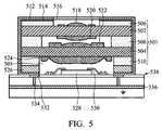
- FIG. 5shows an electronic assembly for an image sensing device of yet another embodiment of the invention.
- a conductive feetis attached to the lens set and the image sensing device is packaged as a chip on board (COB) structure in the embodiment.
- COBchip on board
- a lens set 501is provided.
- the lens set 501 in the embodimentis formed by wafer-level optics technology, and includes a first substrate 502 with a first surface 518 and a second surface 520 on opposite sides thereof and a second substrate 504 with a third surface 522 and a fourth surface 524 on opposite sides thereof. Note that the invention is not limited to the lens set including four surfaces and two substrates shown in the FIG. 5 .
- the lens setcan be single-sided lens or double-sided lens with a least one aperture.
- a first spacer 506is disposed on the first substrate 502
- a second spacer 508is interposed between the first substrate 502 and the second substrate 504
- a third spacer 510is disposed under the second substrate 504 .
- a conductive feet 526is bonded to the third spacer 510 of the lens set 501 , and the conductive feet 526 encloses a cavity 503 for receiving an image sensing chip 528 .
- the conductive feet 526can be formed of metal with compatible thermal expansion coefficient (CTE) to the lens set 501 .
- the image sensing chip 528is bonded to a printed circuit board (PCB) 538 to form a chip on board package structure (COB).
- a conductive wire 530is connected to a pad (not shown) on the image sensing chip and a pad on the printed circuit board 538 to provide electrical connection therebetween.
- a black coating layer 514such as black photoresist, is formed on a top side and a sidewall of the lens set 501 .
- an opaque conductive layer 512is formed on the top side and the sidewall of the lens set 501 , and the bottom side of the conductive feet 526 .
- the opaque conductive layer 512can be aluminum, copper, nickel, silver or stainless steel in the embodiment and is connected to pads 532 of a printed circuit board (PCB), and electrically connected to a grounding layer 536 through the pads 532 and plugs 534 in a printed circuit board (PCB) to provide ground shielding.
- a transparent conductive layer 516such as indium tin oxide (ITO) is formed on a portion of the top side of the lens set 501 . Due to the opaque conductive layer 512 connected to a grounding layer 536 , the assembled image sensing device of the embodiment of the invention can eliminate EMI from the assembled image sensing device.
- the opaque conductive layer on the lens setcan be connected to the pad of the PCB to provide ground shielding regardless of the chip packaging methods used, including a chip scale package (CSP), a ceramic leaded chip carrier (CLCC) or chip on board (COB). Therefore, the invention can provide more flexible application of image sensing devices.
- CSPchip scale package
- CLCCceramic leaded chip carrier
- COBchip on board
Landscapes
- Engineering & Computer Science (AREA)
- Multimedia (AREA)
- Signal Processing (AREA)
- Solid State Image Pick-Up Elements (AREA)
Abstract
Description
Claims (18)
Priority Applications (3)
| Application Number | Priority Date | Filing Date | Title |
|---|---|---|---|
| US12/553,362US8351219B2 (en) | 2009-09-03 | 2009-09-03 | Electronic assembly for an image sensing device |
| TW099103456ATWI411295B (en) | 2009-09-03 | 2010-02-05 | Image sensing component electronic device, wafer level lens group |
| CN2010101252891ACN102005437B (en) | 2009-09-03 | 2010-02-24 | Electronic device for image sensing element, wafer-level lens group |
Applications Claiming Priority (1)
| Application Number | Priority Date | Filing Date | Title |
|---|---|---|---|
| US12/553,362US8351219B2 (en) | 2009-09-03 | 2009-09-03 | Electronic assembly for an image sensing device |
Publications (2)
| Publication Number | Publication Date |
|---|---|
| US20110051390A1 US20110051390A1 (en) | 2011-03-03 |
| US8351219B2true US8351219B2 (en) | 2013-01-08 |
Family
ID=43624632
Family Applications (1)
| Application Number | Title | Priority Date | Filing Date |
|---|---|---|---|
| US12/553,362Active2030-12-18US8351219B2 (en) | 2009-09-03 | 2009-09-03 | Electronic assembly for an image sensing device |
Country Status (3)
| Country | Link |
|---|---|
| US (1) | US8351219B2 (en) |
| CN (1) | CN102005437B (en) |
| TW (1) | TWI411295B (en) |
Cited By (6)
| Publication number | Priority date | Publication date | Assignee | Title |
|---|---|---|---|---|
| US20110261253A1 (en)* | 2010-04-26 | 2011-10-27 | Hon Hai Precision Industry Co., Ltd. | Camera module |
| US20120146170A1 (en)* | 2009-06-08 | 2012-06-14 | Stmicroelectronics (Grenoble 2) Sas | Manufacturing of a camera module |
| US20150243703A1 (en)* | 2011-06-03 | 2015-08-27 | Visera Technologies Company Limited | Methods of fabricating camera module and spacer of a lens structure in the camera module |
| US20170208692A1 (en)* | 2014-07-25 | 2017-07-20 | Lg Innotek Co., Ltd | Printed circuit board |
| US10622526B2 (en)* | 2017-05-07 | 2020-04-14 | Yang Wang | Light emitting device and method for manufacturing light emitting device |
| US11063083B2 (en) | 2019-10-11 | 2021-07-13 | Omnivision Technologies, Inc. | Light-shielded cameras and methods of manufacture |
Families Citing this family (41)
| Publication number | Priority date | Publication date | Assignee | Title |
|---|---|---|---|---|
| CN101990058A (en)* | 2009-07-30 | 2011-03-23 | 鸿富锦精密工业(深圳)有限公司 | Method of coating wafer-level camera module and wafer-level camera module |
| JP5794032B2 (en)* | 2011-08-12 | 2015-10-14 | ソニー株式会社 | OPTICAL UNIT, OPTICAL UNIT MANUFACTURING METHOD, AND IMAGING DEVICE |
| US20130083229A1 (en)* | 2011-09-30 | 2013-04-04 | Omnivision Technologies, Inc. | Emi shield for camera module |
| CN103200474A (en)* | 2012-01-04 | 2013-07-10 | 苏州恒听电子有限公司 | Micro circuit board device used for minitype loudspeaker device |
| MX389501B (en) | 2012-07-26 | 2025-03-20 | Depuy Synthes Products Inc | CONTINUOUS VIDEO IN A LIGHT-POOR ENVIRONMENT |
| MX346174B (en) | 2012-07-26 | 2017-03-10 | Depuy Synthes Products Inc | YCBCR PULSED LIGHTING SCHEME IN A DEFICIENT LIGHT ENVIRONMENT. |
| KR20140019535A (en)* | 2012-08-06 | 2014-02-17 | 엘지이노텍 주식회사 | Camera module and electronic device |
| CN102881704A (en)* | 2012-10-18 | 2013-01-16 | 日月光半导体制造股份有限公司 | Light sensing type semiconductor packaging piece and manufacturing method thereof |
| JP6034725B2 (en)* | 2013-03-05 | 2016-11-30 | 太陽誘電株式会社 | The camera module |
| WO2014144947A1 (en) | 2013-03-15 | 2014-09-18 | Olive Medical Corporation | Super resolution and color motion artifact correction in a pulsed color imaging system |
| CA2906821A1 (en) | 2013-03-15 | 2014-09-18 | Olive Medical Corporation | Scope sensing in a light controlled environment |
| WO2014145249A1 (en) | 2013-03-15 | 2014-09-18 | Olive Medical Corporation | Controlling the integral light energy of a laser pulse |
| US9094593B2 (en) | 2013-07-30 | 2015-07-28 | Heptagon Micro Optics Pte. Ltd. | Optoelectronic modules that have shielding to reduce light leakage or stray light, and fabrication methods for such modules |
| CN109400847B (en)* | 2013-12-26 | 2021-05-18 | 株式会社大赛璐 | Curable composition for lens, and optical device |
| WO2015143453A1 (en) | 2014-03-21 | 2015-09-24 | Olive Medical Corporation | Card edge connector for an imaging sensor |
| CN103916577B (en)* | 2014-03-24 | 2018-06-15 | 南昌欧菲光电技术有限公司 | Electrostatic conducting element and the camera module with the electrostatic conducting element |
| CN103956366B (en)* | 2014-05-20 | 2017-03-29 | 苏州科阳光电科技有限公司 | Wafer stage chip encapsulating structure |
| US9467606B2 (en)* | 2014-06-10 | 2016-10-11 | Omnivision Technologies, Inc. | Wafer level stepped sensor holder |
| US9735135B2 (en)* | 2014-12-04 | 2017-08-15 | Pixart Imaging (Penang) Sdn. Bhd. | Optical sensor package and optical sensor assembly |
| KR102332768B1 (en)* | 2015-02-16 | 2021-11-30 | 삼성전자주식회사 | Camera device and electronic device therefof |
| TWI585870B (en)* | 2015-05-20 | 2017-06-01 | 精材科技股份有限公司 | Chip package and method of manufacturing same |
| US20180247962A1 (en)* | 2015-08-28 | 2018-08-30 | China Wafer Level Csp Co., Ltd. | Image sensor package structure and packaging method thereof |
| US10666841B2 (en)* | 2015-11-11 | 2020-05-26 | Boston Scientific Scimed, Inc. | Visualization device and related systems and methods |
| WO2017081840A1 (en)* | 2015-11-12 | 2017-05-18 | ソニー株式会社 | Solid-state imaging device and solid-state imaging apparatus |
| CN105472217B (en)* | 2015-12-01 | 2021-01-26 | 宁波舜宇光电信息有限公司 | Electrical support with EMI shielding conductive layer, camera module and assembly method thereof |
| WO2017092695A2 (en)* | 2015-12-01 | 2017-06-08 | 宁波舜宇光电信息有限公司 | Image capturing module and electrical support thereof |
| TWI746620B (en)* | 2016-09-23 | 2021-11-21 | 日商索尼半導體解決方案公司 | Camera module, manufacturing method and electronic machine |
| KR102645353B1 (en)* | 2016-12-23 | 2024-03-08 | 삼성전자주식회사 | Camera module |
| EP3707750B1 (en)* | 2017-11-07 | 2024-12-04 | AMS Sensors Singapore Pte. Ltd. | Optoelectronic modules having locking assemblies and methods for manufacturing the same |
| JP6780671B2 (en)* | 2018-03-15 | 2020-11-04 | オムロン株式会社 | Crew monitoring device |
| TWI678570B (en)* | 2018-06-06 | 2019-12-01 | 鴻海精密工業股份有限公司 | Connection structure and camera module using same |
| TWI681424B (en)* | 2018-06-11 | 2020-01-01 | 海華科技股份有限公司 | Optical element, optical component and optical module |
| JP2020047651A (en)* | 2018-09-14 | 2020-03-26 | キオクシア株式会社 | Semiconductor device |
| JP7019203B2 (en)* | 2018-09-21 | 2022-02-15 | 中芯集成電路(寧波)有限公司上海分公司 | Image sensor module and its manufacturing method |
| KR102333727B1 (en)* | 2018-09-21 | 2021-12-01 | 닝보 세미컨덕터 인터내셔널 코포레이션 (상하이 브랜치) | Image sensor module and manufacturing method thereof |
| CN109890188B (en)* | 2019-02-15 | 2021-03-23 | 华为技术有限公司 | Packaging assembly and electronic equipment |
| CN111863756B (en)* | 2019-04-24 | 2022-08-26 | 江苏长电科技股份有限公司 | Packaging structure and semiconductor device with same |
| US11206732B2 (en) | 2019-07-02 | 2021-12-21 | Waymo Llc | Reliable interconnect for camera image sensors |
| CN110783317A (en)* | 2019-10-11 | 2020-02-11 | 安徽国晶微电子有限公司 | Photosensitive chip packaging structure |
| USD928732S1 (en)* | 2020-03-20 | 2021-08-24 | Yubico Ab | Bezel for attaching sensor to a printed circuit board in a security key |
| CN112151562B (en)* | 2020-09-11 | 2023-08-22 | 安徽龙芯微科技有限公司 | Pad through-hole packaging equipment for image sensor chip processing |
Citations (17)
| Publication number | Priority date | Publication date | Assignee | Title |
|---|---|---|---|---|
| US5345324A (en)* | 1992-04-22 | 1994-09-06 | International Business Machines Corporation | Active matrix liquid crystal display device having two light shielding layers |
| US20030124762A1 (en)* | 2001-12-27 | 2003-07-03 | Nobuaki Hashimoto | Optical device and method of manufacturing the same, optical module, circuit board, and electronic instrument |
| US20050056769A1 (en)* | 2003-09-16 | 2005-03-17 | Wen-Ching Chen | Chip scale package structure for an image |
| US20060044450A1 (en)* | 2002-09-17 | 2006-03-02 | Koninklijke Philips Electronics, N.C. | Camera device, method of manufacturing a camera device, wafer scale package |
| US20060043886A1 (en)* | 2004-08-30 | 2006-03-02 | Au Optronics Corp. | Electro-luminescent display device and method for fabricating the same |
| US20060202293A1 (en)* | 2003-09-26 | 2006-09-14 | Danut Bogdan | Optical module and optical system |
| US20060226452A1 (en)* | 2005-04-08 | 2006-10-12 | Konica Minolta Opto, Inc. | Solid-state image pickup device and the manufacture method thereof |
| US20070090478A1 (en)* | 2005-10-18 | 2007-04-26 | Po-Hung Chen | Image sensor package structure |
| US20070216028A1 (en)* | 2006-03-14 | 2007-09-20 | Samsung Electronics Co., Ltd. | Micro-element package and manufacturing method thereof |
| US20080061425A1 (en)* | 2006-09-13 | 2008-03-13 | United Microdisplay Optronics Corp. | Chip package structure and fabricating method thereof |
| US20080164550A1 (en)* | 2007-01-08 | 2008-07-10 | Visera Technologies Company Limited | Electronic assembly for image sensor device and fabrication method thereof |
| US20080218623A1 (en)* | 2007-03-09 | 2008-09-11 | Hon Hai Precision Industry Co., Ltd. | Accurately-aligned camera module and method for making same |
| US20090134483A1 (en)* | 2007-11-23 | 2009-05-28 | Jui-Ping Weng | Electronic assembly for image sensor device |
| US20090256931A1 (en)* | 2008-04-11 | 2009-10-15 | Samsung Electronics Co., Ltd. | Camera module, method of manufacturing the same, and electronic system having the same |
| US20090321861A1 (en)* | 2008-06-26 | 2009-12-31 | Micron Technology, Inc. | Microelectronic imagers with stacked lens assemblies and processes for wafer-level packaging of microelectronic imagers |
| US20110032409A1 (en)* | 2007-12-19 | 2011-02-10 | Heptagon Oy | Optical module for a camera device, baffle substrate, wafer scale package, and manufacturing methods therefor |
| US20110050979A1 (en)* | 2007-12-19 | 2011-03-03 | Heptagon Oy | Optical module, wafer scale package, and method for manufacturing those |
Family Cites Families (1)
| Publication number | Priority date | Publication date | Assignee | Title |
|---|---|---|---|---|
| KR100664316B1 (en)* | 2004-12-23 | 2007-01-04 | 삼성전자주식회사 | Image sensor package, solid state imaging device and manufacturing method thereof |
- 2009
- 2009-09-03USUS12/553,362patent/US8351219B2/enactiveActive
- 2010
- 2010-02-05TWTW099103456Apatent/TWI411295B/enactive
- 2010-02-24CNCN2010101252891Apatent/CN102005437B/enactiveActive
Patent Citations (17)
| Publication number | Priority date | Publication date | Assignee | Title |
|---|---|---|---|---|
| US5345324A (en)* | 1992-04-22 | 1994-09-06 | International Business Machines Corporation | Active matrix liquid crystal display device having two light shielding layers |
| US20030124762A1 (en)* | 2001-12-27 | 2003-07-03 | Nobuaki Hashimoto | Optical device and method of manufacturing the same, optical module, circuit board, and electronic instrument |
| US20060044450A1 (en)* | 2002-09-17 | 2006-03-02 | Koninklijke Philips Electronics, N.C. | Camera device, method of manufacturing a camera device, wafer scale package |
| US20050056769A1 (en)* | 2003-09-16 | 2005-03-17 | Wen-Ching Chen | Chip scale package structure for an image |
| US20060202293A1 (en)* | 2003-09-26 | 2006-09-14 | Danut Bogdan | Optical module and optical system |
| US20060043886A1 (en)* | 2004-08-30 | 2006-03-02 | Au Optronics Corp. | Electro-luminescent display device and method for fabricating the same |
| US20060226452A1 (en)* | 2005-04-08 | 2006-10-12 | Konica Minolta Opto, Inc. | Solid-state image pickup device and the manufacture method thereof |
| US20070090478A1 (en)* | 2005-10-18 | 2007-04-26 | Po-Hung Chen | Image sensor package structure |
| US20070216028A1 (en)* | 2006-03-14 | 2007-09-20 | Samsung Electronics Co., Ltd. | Micro-element package and manufacturing method thereof |
| US20080061425A1 (en)* | 2006-09-13 | 2008-03-13 | United Microdisplay Optronics Corp. | Chip package structure and fabricating method thereof |
| US20080164550A1 (en)* | 2007-01-08 | 2008-07-10 | Visera Technologies Company Limited | Electronic assembly for image sensor device and fabrication method thereof |
| US20080218623A1 (en)* | 2007-03-09 | 2008-09-11 | Hon Hai Precision Industry Co., Ltd. | Accurately-aligned camera module and method for making same |
| US20090134483A1 (en)* | 2007-11-23 | 2009-05-28 | Jui-Ping Weng | Electronic assembly for image sensor device |
| US20110032409A1 (en)* | 2007-12-19 | 2011-02-10 | Heptagon Oy | Optical module for a camera device, baffle substrate, wafer scale package, and manufacturing methods therefor |
| US20110050979A1 (en)* | 2007-12-19 | 2011-03-03 | Heptagon Oy | Optical module, wafer scale package, and method for manufacturing those |
| US20090256931A1 (en)* | 2008-04-11 | 2009-10-15 | Samsung Electronics Co., Ltd. | Camera module, method of manufacturing the same, and electronic system having the same |
| US20090321861A1 (en)* | 2008-06-26 | 2009-12-31 | Micron Technology, Inc. | Microelectronic imagers with stacked lens assemblies and processes for wafer-level packaging of microelectronic imagers |
Cited By (9)
| Publication number | Priority date | Publication date | Assignee | Title |
|---|---|---|---|---|
| US20120146170A1 (en)* | 2009-06-08 | 2012-06-14 | Stmicroelectronics (Grenoble 2) Sas | Manufacturing of a camera module |
| US8575712B2 (en)* | 2009-06-08 | 2013-11-05 | Stmicroelectronics (Grenoble 2) Sas | Manufacturing of a camera module |
| US20110261253A1 (en)* | 2010-04-26 | 2011-10-27 | Hon Hai Precision Industry Co., Ltd. | Camera module |
| US20150243703A1 (en)* | 2011-06-03 | 2015-08-27 | Visera Technologies Company Limited | Methods of fabricating camera module and spacer of a lens structure in the camera module |
| US9502461B2 (en)* | 2011-06-03 | 2016-11-22 | Visera Technologies Company Limited | Methods of fabricating camera module and spacer of a lens structure in the camera module |
| US20170208692A1 (en)* | 2014-07-25 | 2017-07-20 | Lg Innotek Co., Ltd | Printed circuit board |
| US10064280B2 (en)* | 2014-07-25 | 2018-08-28 | Lg Innotek Co., Ltd. | Printed circuit board |
| US10622526B2 (en)* | 2017-05-07 | 2020-04-14 | Yang Wang | Light emitting device and method for manufacturing light emitting device |
| US11063083B2 (en) | 2019-10-11 | 2021-07-13 | Omnivision Technologies, Inc. | Light-shielded cameras and methods of manufacture |
Also Published As
| Publication number | Publication date |
|---|---|
| US20110051390A1 (en) | 2011-03-03 |
| CN102005437A (en) | 2011-04-06 |
| TW201110676A (en) | 2011-03-16 |
| CN102005437B (en) | 2012-09-19 |
| TWI411295B (en) | 2013-10-01 |
Similar Documents
| Publication | Publication Date | Title |
|---|---|---|
| US8351219B2 (en) | Electronic assembly for an image sensing device | |
| US7679167B2 (en) | Electronic assembly for image sensor device and fabrication method thereof | |
| US7829966B2 (en) | Electronic assembly for image sensor device | |
| CN103066061B (en) | Camera model and include the system of camera model | |
| KR100909970B1 (en) | Camera module | |
| US8902356B2 (en) | Image sensor module having image sensor package | |
| US8107005B2 (en) | Method of manufacturing an image sensor module | |
| US20110285890A1 (en) | Camera module | |
| KR101070058B1 (en) | Camera Module Package | |
| US7566854B2 (en) | Image sensor module | |
| KR20150030904A (en) | Camera module | |
| US8023019B2 (en) | Image-sensing chip package module for reducing its whole thickness | |
| JP2005348275A (en) | Image sensor and camera module | |
| US20050211888A1 (en) | Solid state imaging device | |
| US9111826B2 (en) | Image pickup device, image pickup module, and camera | |
| CN100544011C (en) | Image sensing device and manufacturing method thereof | |
| US20060289733A1 (en) | Stack-type image sensor module | |
| KR20080081726A (en) | Image sensor module and camera module having same | |
| US20140132813A1 (en) | Camera module having passive components | |
| JP2013005116A (en) | Camera module and electronic apparatus including the same | |
| KR100968971B1 (en) | Image sensor module | |
| HK1181919A (en) | Camera module and system comprising the same | |
| HK1181919B (en) | Camera module and system comprising the same | |
| KR20120066391A (en) | Camera module |
Legal Events
| Date | Code | Title | Description |
|---|---|---|---|
| AS | Assignment | Owner name:VISERA TECHNOLOGIES COMPANY LIMITED, TAIWAN Free format text:ASSIGNMENT OF ASSIGNORS INTEREST;ASSIGNORS:LIN, CHUN-CHI;DENG, JAU-JAN;CHEN, WEI-PING;REEL/FRAME:023191/0634 Effective date:20090821 | |
| AS | Assignment | Owner name:OMNIVISION TECHNOLOGIES, INC., CALIFORNIA Free format text:ASSIGNMENT OF ASSIGNORS INTEREST;ASSIGNOR:VISERA TECHNOLOGIES COMPANY LIMITED;REEL/FRAME:026563/0895 Effective date:20110624 | |
| AS | Assignment | Owner name:VISERA TECHNOLOGIES COMPANY LIMITED, TAIWAN Free format text:CORRECTIVE ASSIGNMENT TO CORRECT THE ASSIGNEE PREVIOUSLY RECORDED ON REEL 026563 FRAME 0895. ASSIGNOR(S) HEREBY CONFIRMS THE ASSIGNEES ARE OMNIVISION TECHNOLOGIES, INC. AND VISERA TECHNOLOGIES COMPANY LIMITED;ASSIGNOR:VISERA TECHNOLOGIES COMPANY LIMITED;REEL/FRAME:026736/0545 Effective date:20110624 Owner name:OMNIVISION TECHNOLOGIES, INC., CALIFORNIA Free format text:CORRECTIVE ASSIGNMENT TO CORRECT THE ASSIGNEE PREVIOUSLY RECORDED ON REEL 026563 FRAME 0895. ASSIGNOR(S) HEREBY CONFIRMS THE ASSIGNEES ARE OMNIVISION TECHNOLOGIES, INC. AND VISERA TECHNOLOGIES COMPANY LIMITED;ASSIGNOR:VISERA TECHNOLOGIES COMPANY LIMITED;REEL/FRAME:026736/0545 Effective date:20110624 | |
| STCF | Information on status: patent grant | Free format text:PATENTED CASE | |
| FPAY | Fee payment | Year of fee payment:4 | |
| MAFP | Maintenance fee payment | Free format text:PAYMENT OF MAINTENANCE FEE, 8TH YEAR, LARGE ENTITY (ORIGINAL EVENT CODE: M1552); ENTITY STATUS OF PATENT OWNER: LARGE ENTITY Year of fee payment:8 | |
| MAFP | Maintenance fee payment | Free format text:PAYMENT OF MAINTENANCE FEE, 12TH YEAR, LARGE ENTITY (ORIGINAL EVENT CODE: M1553); ENTITY STATUS OF PATENT OWNER: LARGE ENTITY Year of fee payment:12 |