US8350831B2 - Method and apparatus for detecting a multitouch event in an optical touch-sensitive device - Google Patents
Method and apparatus for detecting a multitouch event in an optical touch-sensitive deviceDownload PDFInfo
- Publication number
- US8350831B2 US8350831B2US13/059,817US200913059817AUS8350831B2US 8350831 B2US8350831 B2US 8350831B2US 200913059817 AUS200913059817 AUS 200913059817AUS 8350831 B2US8350831 B2US 8350831B2
- Authority
- US
- United States
- Prior art keywords
- beams
- touch point
- point
- predetermined
- candidate
- Prior art date
- Legal status (The legal status is an assumption and is not a legal conclusion. Google has not performed a legal analysis and makes no representation as to the accuracy of the status listed.)
- Active
Links
Images


Classifications
- G—PHYSICS
- G06—COMPUTING OR CALCULATING; COUNTING
- G06F—ELECTRIC DIGITAL DATA PROCESSING
- G06F3/00—Input arrangements for transferring data to be processed into a form capable of being handled by the computer; Output arrangements for transferring data from processing unit to output unit, e.g. interface arrangements
- G06F3/01—Input arrangements or combined input and output arrangements for interaction between user and computer
- G06F3/03—Arrangements for converting the position or the displacement of a member into a coded form
- G06F3/041—Digitisers, e.g. for touch screens or touch pads, characterised by the transducing means
- G06F3/0416—Control or interface arrangements specially adapted for digitisers
- G06F3/0418—Control or interface arrangements specially adapted for digitisers for error correction or compensation, e.g. based on parallax, calibration or alignment
- G06F3/04186—Touch location disambiguation
- G—PHYSICS
- G06—COMPUTING OR CALCULATING; COUNTING
- G06F—ELECTRIC DIGITAL DATA PROCESSING
- G06F3/00—Input arrangements for transferring data to be processed into a form capable of being handled by the computer; Output arrangements for transferring data from processing unit to output unit, e.g. interface arrangements
- G06F3/01—Input arrangements or combined input and output arrangements for interaction between user and computer
- G06F3/03—Arrangements for converting the position or the displacement of a member into a coded form
- G06F3/041—Digitisers, e.g. for touch screens or touch pads, characterised by the transducing means
- G06F3/0416—Control or interface arrangements specially adapted for digitisers
- G06F3/04166—Details of scanning methods, e.g. sampling time, grouping of sub areas or time sharing with display driving
- G—PHYSICS
- G06—COMPUTING OR CALCULATING; COUNTING
- G06F—ELECTRIC DIGITAL DATA PROCESSING
- G06F3/00—Input arrangements for transferring data to be processed into a form capable of being handled by the computer; Output arrangements for transferring data from processing unit to output unit, e.g. interface arrangements
- G06F3/01—Input arrangements or combined input and output arrangements for interaction between user and computer
- G06F3/03—Arrangements for converting the position or the displacement of a member into a coded form
- G06F3/041—Digitisers, e.g. for touch screens or touch pads, characterised by the transducing means
- G06F3/042—Digitisers, e.g. for touch screens or touch pads, characterised by the transducing means by opto-electronic means
- G06F3/0421—Digitisers, e.g. for touch screens or touch pads, characterised by the transducing means by opto-electronic means by interrupting or reflecting a light beam, e.g. optical touch-screen
- G—PHYSICS
- G06—COMPUTING OR CALCULATING; COUNTING
- G06F—ELECTRIC DIGITAL DATA PROCESSING
- G06F3/00—Input arrangements for transferring data to be processed into a form capable of being handled by the computer; Output arrangements for transferring data from processing unit to output unit, e.g. interface arrangements
- G06F3/01—Input arrangements or combined input and output arrangements for interaction between user and computer
- G06F3/03—Arrangements for converting the position or the displacement of a member into a coded form
- G06F3/041—Digitisers, e.g. for touch screens or touch pads, characterised by the transducing means
- G06F3/0416—Control or interface arrangements specially adapted for digitisers
- G06F3/0418—Control or interface arrangements specially adapted for digitisers for error correction or compensation, e.g. based on parallax, calibration or alignment
- G—PHYSICS
- G06—COMPUTING OR CALCULATING; COUNTING
- G06F—ELECTRIC DIGITAL DATA PROCESSING
- G06F3/00—Input arrangements for transferring data to be processed into a form capable of being handled by the computer; Output arrangements for transferring data from processing unit to output unit, e.g. interface arrangements
- G06F3/01—Input arrangements or combined input and output arrangements for interaction between user and computer
- G06F3/03—Arrangements for converting the position or the displacement of a member into a coded form
- G06F3/041—Digitisers, e.g. for touch screens or touch pads, characterised by the transducing means
- G06F3/042—Digitisers, e.g. for touch screens or touch pads, characterised by the transducing means by opto-electronic means
- G06F3/0428—Digitisers, e.g. for touch screens or touch pads, characterised by the transducing means by opto-electronic means by sensing at the edges of the touch surface the interruption of optical paths, e.g. an illumination plane, parallel to the touch surface which may be virtual
- G—PHYSICS
- G06—COMPUTING OR CALCULATING; COUNTING
- G06F—ELECTRIC DIGITAL DATA PROCESSING
- G06F3/00—Input arrangements for transferring data to be processed into a form capable of being handled by the computer; Output arrangements for transferring data from processing unit to output unit, e.g. interface arrangements
- G06F3/01—Input arrangements or combined input and output arrangements for interaction between user and computer
- G06F3/048—Interaction techniques based on graphical user interfaces [GUI]
- G06F3/0487—Interaction techniques based on graphical user interfaces [GUI] using specific features provided by the input device, e.g. functions controlled by the rotation of a mouse with dual sensing arrangements, or of the nature of the input device, e.g. tap gestures based on pressure sensed by a digitiser
- G06F3/0488—Interaction techniques based on graphical user interfaces [GUI] using specific features provided by the input device, e.g. functions controlled by the rotation of a mouse with dual sensing arrangements, or of the nature of the input device, e.g. tap gestures based on pressure sensed by a digitiser using a touch-screen or digitiser, e.g. input of commands through traced gestures
- G06F3/04883—Interaction techniques based on graphical user interfaces [GUI] using specific features provided by the input device, e.g. functions controlled by the rotation of a mouse with dual sensing arrangements, or of the nature of the input device, e.g. tap gestures based on pressure sensed by a digitiser using a touch-screen or digitiser, e.g. input of commands through traced gestures for inputting data by handwriting, e.g. gesture or text
- G—PHYSICS
- G06—COMPUTING OR CALCULATING; COUNTING
- G06F—ELECTRIC DIGITAL DATA PROCESSING
- G06F2203/00—Indexing scheme relating to G06F3/00 - G06F3/048
- G06F2203/041—Indexing scheme relating to G06F3/041 - G06F3/045
- G06F2203/04104—Multi-touch detection in digitiser, i.e. details about the simultaneous detection of a plurality of touching locations, e.g. multiple fingers or pen and finger
- G—PHYSICS
- G06—COMPUTING OR CALCULATING; COUNTING
- G06F—ELECTRIC DIGITAL DATA PROCESSING
- G06F2203/00—Indexing scheme relating to G06F3/00 - G06F3/048
- G06F2203/041—Indexing scheme relating to G06F3/041 - G06F3/045
- G06F2203/04108—Touchless 2D- digitiser, i.e. digitiser detecting the X/Y position of the input means, finger or stylus, also when it does not touch, but is proximate to the digitiser's interaction surface without distance measurement in the Z direction
- G—PHYSICS
- G06—COMPUTING OR CALCULATING; COUNTING
- G06F—ELECTRIC DIGITAL DATA PROCESSING
- G06F2203/00—Indexing scheme relating to G06F3/00 - G06F3/048
- G06F2203/048—Indexing scheme relating to G06F3/048
- G06F2203/04808—Several contacts: gestures triggering a specific function, e.g. scrolling, zooming, right-click, when the user establishes several contacts with the surface simultaneously; e.g. using several fingers or a combination of fingers and pen
Definitions
- the present inventionrelates to a method and apparatus for detecting a touch point in a touch-sensitive device.
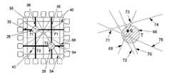
- optical emitters 14 , 22 and detectors 18 , 24are arranged along opposite edges of a rectangular touch sensitive surface 16 and an orthogonal grid is formed by the optical beams 12 , 20 transmitted between the emitters and the corresponding detectors.
- beammeans the light passing along a narrow optical path between an emitter and a detector, and does not imply that any given emitter necessarily emits light in one or more discrete, directed beams although, in the case of FIG. 1 , each emitter only emits light over a narrow angle to ensure that only the directly opposite detector receives light from it.
- the term “light”includes IR and UV radiation, and the term “optical” is to be interpreted accordingly.
- the touch sensitive surfacemay be an optically transparent planar waveguide through which the beams pass by total internal reflection, or a surface over which the beams pass in close proximity to the surface and substantially parallel to the surface.
- the material usedcould be a transparent sheet of plastic or glass.
- An objectsuch as a finger or a stylus coming into contact with the transparent waveguide will have a higher refractive index than the air normally surrounding the waveguide. Over the area of contact, the increase in refractive index will disturb the total internal reflection of the beams within the waveguide. The disruption of total internal reflection increases the light leakage from the waveguide, attenuating any beams passing through the position of the touch event. Correspondingly, the removal of the touching object will cause the attenuation of the passing beams to be reduced. Such changes in attenuation are detectable at the output of the associated detectors.
- a beamis deemed interrupted if its amplitude, as detected by the relevant detector, falls below a predetermined or adaptively calculated threshold value T h .
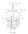
- the emitters 14 , 22 and detectors 18 , 24are driven by a controller 200 via drive circuits 210 .
- the controller 200which may, for example, comprise a suitably programmed microprocessor or a PLA, also serves to process the data output from the detectors, after analogue to digital conversion, to determine the location of a touch point.
- the beamsare scanned in sequence and logic in the CPU can determine the intersection point of one or more interrupted beams and deduce the position of the interrupting object.
- the objectmust be large enough to detectably attenuate at least one beam in one axis and at least one beam in the orthogonal axis, so resolution is typically quite poor unless large numbers of emitters and/or detectors are used.
- scanning the beamswe mean sampling the detector outputs to determine the amplitude of the, or each, beam falling on each detector.
- orthogonal grid of beamsis effective when at most one opaque object is to be located in the touch sensitive area because the central position of that object can be completely described by a pair of orthogonal coordinates yielded by the scanning process.
- U.S. Pat. No. 4,301,447discloses a mechanism for detecting the interruption of the beams between any given emitter and some or all of the detectors along the opposing edge of the touch sensitive surface for the purposes of increasing the resolution of the touch sensing mechanism.
- Patents EP 0601651A1 and U.S. Pat. No. 5,635,724disclose methods for processing the detector outputs from such a scanning system in order to resolve the centrelines of the shadows cast when an interrupting object is placed in the path of an emitter with a diverging pattern of radiation.
- the resolutionis improved, but there is no accommodation for multiple simultaneous touch events.
- the coordinates generated by such a system in the presence of more than one interrupting object 26 , 28can be ambiguous because the beams associated with one touch point could intersect with the beams of another touch point and indicate the possible presence of at least one false additional touch point.
- two pairs of interrupted orthogonal beamscould indicate between two and four simultaneous touch events at the corners of the rectangle described by the four intersecting beams.
- two touch events 26 and 28 at locations T 1 and T 2 respectively in the touch sensitive surface 30interrupt beams 32 and 34 in one axis and beams 36 and 38 in the other axis. It is evident from the drawing that with only this information, associated logic circuitry cannot determine with certainty whether there are touch events at locations T 1 and T 2 or at locations F 1 and F 2 or at some combination of these locations which is consistent with the interruption of the four beams 32 , 34 , 36 and 38 .
- IBM Technical Disclosure Bulletin Vol. 28, No. 4, September 1985 pages 1760-1762(“Enhanced Optical Touch Input Panel”), M. Johnson, discloses the use of a bitmap of the touch sensitive surface onto which is mapped the triangular shadow areas of such diverging interrupted beams from successively activated emitters around the periphery of the touch sensitive surface.
- the method disclosedconsists of initialising all of the bitmap points to the same value at the outset and setting the bitmap points to the opposite value at all the points along beams which are not interrupted when the first emitter is activated. Subsequently, the first emitter is deactivated and the next emitter is activated and again any points along beams, which are not interrupted are set to the opposite value to that set at initialisation.
- the final bitmapwill retain the initialised values only in those points which are traversed by beams which were interrupted for all emitter activation times and so are most likely to correspond to real touch events.
- a method for determining a touch point in a touch-sensitive optical devicecomprising a plurality of optical emitters and a plurality of optical detectors, the optical emitters and the optical detectors defining therebetween a plurality of optical beam paths forming an optical beam intersection pattern extending over an area, the method comprising the steps of:
- said step of assigningis based on a function of the degree of modulation of the predetermined other beams.
- the contributions of the predetermined other beamsare weighted in said function dependent on the degree of modulation.
- the weighting for each predetermined other beamdepends upon one or more of: the proximity of the predetermined other beam to the candidate touch point; the angle of the predetermined other beam to the angle of the beams defining the candidate touch point; and the number of predetermined other beams.
- the step of analyzingis based on predetermined other beam intersection points near to or coincident with said candidate touch point.
- the methodfurther comprises the step of retrieving stored data from a database defining the predetermined other beams or predetermined other beam intersections for each beam intersection point, said step of analyzing based at least in part on said stored data.
- the stored dataincludes respective weighting and/or proximity values relating to the predetermined other beams or predetermined other beam intersections.
- the beam intersection patternis symmetrical about at least one axis of the area of optical beam paths, wherein said step of retrieving comprises retrieving stored data regarding beams on one side of said at least one axis, the method further comprising the step of extrapolating the beam data for the beams on the symmetrically opposite side of said at least one axis based on said stored data.
- the methodfurther comprises the step of designating said modulation as an interruption of the beam if said modulation exceeds a threshold level, and wherein in said step of assigning, said candidate touch point is assigned at the intersection of a pair of interrupted beams.
- said threshold levelis an adaptive threshold level.
- said step of designatingcomprises comparing the detected modulation with a predefined modulation level for that touch point region.
- the methodcomprises the step of retrieving data indicative of a typical modulation level for an actual touch point for that touch point region.
- said datacomprises one or more of the following: the number of beams passing through the touch point region; the number of intersections of beams falling within the touch point region; or maximum modulation to be expected in the touch point region.
- the methodfurther comprises the step of grouping actual touch points into clusters based on a search radius distance from a cluster member to at least one other member of the same cluster.
- said beam intersection patternis non-uniform and said search radius distance varies according to the position of the cluster member in the beam intersection pattern.
- the methodfurther comprises the step of estimating the centre of a cluster as the average position of all of the cluster members.
- the methodfurther comprises the step of estimating the centre of a cluster as the centre of a bounding rectangle around the cluster.
- the methodfurther comprises the step of estimating the centre of a cluster as the average position of outlying cluster members.
- said estimation stepis based on a weighted average, the weights depending on the degree of modulation of the beams at each point contributing to the average.
- the methodfurther comprises the step of determining the orientation of a non-circular touch contact area.
- the orientationis determined by mathematically rotating at least two confirmed touch points lying on or near the perimeter of the contact area around the estimated centre of the contact area and determining the minimum or maximum average absolute value of the distance between each touch point and a fixed axis.
- the methodcomprises the steps of:
- said point validity valueis initialised to 0.
- step (iv)comprises subtracting a threshold value from said measured beam strength.
- step (viii)comprises dividing said point validity value by the number of predetermined other beams.
- the methodfurther comprises the step of storing an indication of said actual touch point in a validated point list.
- the methodfurther comprises the step of determining if a candidate touch point is near the boundary of a touch event, and wherein said steps of analyzing and determining whether the candidate touch point is an actual touch point are carried out only in respect of those candidate touch point near the boundary of a touch event.
- a touch-sensitive optical devicecomprising a plurality of optical emitters and a plurality of optical detectors, the optical emitters and the optical detectors arranged relative to a touchable surface such that energy transmitted by the emitters is received by the detectors along multiple intersecting beams which pass adjacent the surface, and wherein touching the surface at a beam causes a detectable modulation of the energy transmitted along the beam, the device further comprising a processing means operable to perform the following steps:
- a touch sensitive optical control devicecomprises a set of light emitters and a set of light detectors arranged relative to a touchable surface such that light transmitted by the emitters is received by the detectors along multiple intersecting beams which pass transversely of the surface and touching the surface at a beam causes a detectable modulation of the light transmitted along the beam, such modulation if sufficiently large being registered as an interruption of the beam by an associated processing means, wherein the processing means defines candidate touch points at the intersections of interrupted beams and confirms or not each candidate touch point as an actual touch point by examining predetermined other beams (test beams) near to or coincident with the candidate touch point.
- test beam intersection pointsmay optionally be examined to confirm each candidate touch point as an actual touch point.
- the inventionis especially valuable in a multi-touch system, where the intersection of two beams alone may be inconclusive.
- the inventionprovides a low cost optical touch overlay with high resolution and multi-touch capability.
- Embodiments of the inventionprovide further details about the touch points, such as the centre, size and orientation of each touch point contact area as well as the efficient calculation of these values.
- FIG. 1is a schematic diagram of a conventional optical touch sensitive overlay and associated circuitry with an orthogonal arrangement of beams extending between emitters and detectors.
- FIG. 2 ashows the ambiguity which can arise when there are multiple touch points in the overlay of FIG. 1 .
- FIG. 2 bshows the elimination of false touch points in the overlay of FIG. 1 using additional nearby beams.
- FIG. 3is a schematic diagram of an optical touch sensitive overlay used in an embodiment of the invention.
- FIG. 4shows how the axes of the emitters and detectors of FIG. 3 can be orientated relative to the touch sensitive surface for maximum coverage.
- FIG. 5 aillustrates the use of nearby beams to validate a candidate touch point.
- FIG. 5 billustrates the use of nearby beam intersections to validate a candidate touch point.
- FIG. 6 aillustrates the organisation of a lookup table containing beam information used in validation.
- FIG. 6 bis a flowchart of the steps carried out in a validation process.
- FIG. 6 cis a weight table used in validation calculations.
- FIG. 7 aillustrates the preferential validation of boundary points of the contact area of a touch event.
- FIG. 7 bis a modification of the flowchart of FIG. 6 b which implements the principle of FIG. 7 a.
- FIGS. 8 a and 8 bshow how data storage requirements can be reduced by taking advantage of beam symmetry.
- FIG. 9 ashows how validated points relating to a touch event may be gathered into a cluster.
- FIG. 9 bis a flowchart of the clustering process.
- FIG. 10shows a method of estimating the degree of rotational symmetry of a cluster and its orientation.
- FIG. 11shows how the orientation of a cluster which is substantially non-circular can be used as a control value.
- FIG. 12is an embodiment of the invention applied to a single axis scanning system.
- a plurality of beam intersectionsare tested for interruption, where the tested beams are coincident with, or close to, each indicated candidate touch point.
- the principleis shown in FIG. 2 b , where additional beams 40 and 42 , if present, can be used to determine the likelihood of touch events at locations F 1 and F 2 on the touch sensitive surface 30 of FIG. 2 a.
- the beam 40is near to, and almost coincident with, the intersection of the interrupted beams 32 and 38 , so anything other than a very small object present at location F 1 will interrupt beams 32 , 38 and 40 .
- the beam 42is almost coincident with the intersection of interrupted beams 34 and 36 at location F 2 .
- the status of these two additional beams 40 and 42along with the status of the additional beams 54 and 56 passing through T 1 and T 2 , can be used to determine without ambiguity at which of the locations T 1 , T 2 , F 1 and F 2 there are touch events.
- emitters with wide radiant angles and detectors with wide acceptance anglesare arranged around the entire periphery of a touch sensitive surface to maximise the number and angular span of beam angles available to resolve ambiguous beam intersections.
- FIG. 3where a set of intersecting beams 44 pass between emitters 46 with wide radiant angles and detectors 48 with wide acceptance angles across a touch sensitive surface 50 .
- the number of beams 44 available for touch detection and their closely spaced intersectionsoffers the potential to determine object positions with high resolution in those regions although the number of emitters 46 and detectors 48 is the same.
- the emitters and detectorsare equal in number and equally spaced, many of the intersections between beams will be coincident with other beam intersections, which is particularly useful for increasing the accuracy of detection.
- each emitter 46can be directed to be received optimally at the maximum number of detectors 48 by orienting the emitter 46 accordingly or by the use of lenses, waveguides or mirrors.
- the orientation of the acceptance angle of each detector 48can be similarly optimised.
- the array of emitters and detectorsis driven by drive circuits 210 and a controller 200 , generally such as shown and described with respect to FIG. 1 .
- FIG. 5 ashows a touch event 66 which includes a candidate touch point P at the intersection of beams 68 and 70 .
- a candidate touch pointwe mean the intersection point of two interrupted beams.
- a candidate touch pointcan be an actual touch point, as shown in FIG. 5 a where the touch point P is caused by actual interruption of the beams 68 and 70 at the touch event 66 , or it could be caused by the interruption in the beams by touch events elsewhere on the touch sensitive surface.
- two beams which have been interrupted in a way consistent with a touch eventare tested to see if they intersect and if so, the intersection of the pair is considered to be a candidate touch point.
- a candidate pointis validated (confirmed) or eliminated by inspection of coincident or nearby beams (test beams). If an attenuating object is actually present at the candidate touch point, any test beam passing through that point should be similarly interrupted. Test beams which are near to the candidate intersection point will typically exercise a greater influence on the validation process than those which are more distant.
- beams 72 , 74 and 76are tested to see if they are also interrupted and if so, the point P is deemed to be valid. Since none of the beams 72 , 74 or 76 is coincident with the intersection point P of beams 68 and 70 , a weighted sum of their status values is used to determine the likelihood that the candidate point P is valid. Beams 72 and 76 are both interrupted and only beam 74 is not interrupted, so because beams 72 and 76 are both nearer to the candidate touch point P, the present embodiment would deem point P to be valid.
- the weighting value associated with a test beam which is coincident with the candidate touch point, but not interruptedwill normally be set high enough to outweigh the combined validating effect of any number of nearby or coincident beams which are interrupted. This is to ensure that an uninterrupted beam passing through a point prevents that point becoming validated as a touch point. However, there may be circumstances (such as a low signal-to-noise ratio in the scanning mechanism) where a smaller difference between the negating effect of an uninterrupted beam and the validating effect of an interrupted beam is appropriate.
- the beams within close range of a candidate touch pointare tested to determine whether it represents a genuine touch event or not. If a limited number of beams are to be tested for each candidate point to minimise processing time, the beams selected should be chosen at least in part by their angles relative to the angles of the beams in the candidate point; testing with a wide range of beam angles increases the chance of eliminating a false touch point.
- the weighting values for a beamshould include some combination of proximity to candidate touch point, difference in angle from the beams defining the candidate touch point and the number (or density) of beams near to the candidate touch point. Weighting values can be calculated as needed or can be retrieved from lookup tables or lists.
- a candidate pointis validated (confirmed) or eliminated by inspection of coincident or nearby intersection points of beams.
- Test beam intersection points which are near to the candidate pointwill typically exercise a greater influence on the validation process than those which are more distant.
- FIG. 5 bshows intersection points (such as example points 71 and 73 ) which are near to the candidate touch point q which may be used in the validation or elimination of touch point q.
- the test intersection point 71at the intersection of beam 74 and beam 76 , is more distant from candidate touch point q than intersection point 73 at the intersection of beam 68 and beam 74 , and this typically results in the influence of test point 73 on the validation processing being greater than the influence of test point 71 .
- the candidate point qis validated as a real touch point if the nearby and coincident test intersection points are consistent with a touch at candidate touch point q.
- the criteria usedwill be similar to those used for nearby beams, such as the depth of modulation of the beams intersecting at the test intersection point, the angles of the beams intersecting at the test intersection point, the proximity of the test intersection point to the candidate touch point and the number (or density) of beams close to the candidate touch point.
- FIG. 6 ais an example of the structure of such a list.
- each beamcontains a record for every intersection with another beam, as long as there is no duplicate record for the intersection elsewhere in the list.
- Each intersection recordcontains the X and Y coordinates of the intersection and the identities of the nearby/coincident beams to be tested for a candidate touch point at this intersection to be validated. It also holds a weighting code for each test beam, which determines the influence of the test beam status on the validation of the candidate touch point.
- the listalso includes, in each intersection point record, a cluster search radius and a boundary point field, the purpose of which will be described later.
- Such a tablefacilitates the rapid testing of a candidate touch point against many local reference beams or points to see if it represents an actual interruption or is an artefact of other interruptions.
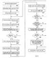
- FIG. 6 bis a flowchart of the steps carried out by the controller 200 in the present embodiment to eliminate or validate a candidate touch point, according to the principles described above.
- a parameter called the validity value of the pointis set to zero at step 602 .
- the identity of the first of the coincident/nearby test beams to be used in validating the candidate touch pointis fetched from the beam intersection list.
- the strength of this test beamis obtained. This value may be a 1-bit binary value of 0 or 1 (1 corresponding to full transmission between the emitter and the detector at each end of the beam) or a higher resolution value in the same range.
- an attenuation marginis calculated by subtracting the threshold value T h from the beam strength (the beam strength is normalised in the range 0-1 and T h is a value between 0 and 1 corresponding to full transmission and complete interruption respectively).
- the beam weight codeis fetched from the beam intersection list and at step 612 the weight code is converted to a weight value using a weight table ( FIG. 6 c ) and the sign of the attenuation margin.
- the weight valueis multiplied by the attenuation margin and the result added to the point validity value at step 616 .
- Step 618tests whether there are more test beams to be evaluated in respect of the current candidate touch point, and steps 604 to 616 are repeated for each test beam.
- step 620divides the cumulative point validity value by the number of test beams used to get the average. If the average is greater than zero, step 622 , the data for that touch point is validated and added to a validated point list, step 624 .
- the result of the processing shown in FIG. 6 bis a validated point list which contains information such as the X and Y coordinates of each point, along with the validity value of each point (a measure of confidence that the point is related to a real touch event) and various other values to be used in subsequent processing stages.
- FIG. 6 cshows an example of the two sets of values used to convert from a weighting code, held in the beam intersection list, to a weighting value used in the validation calculation.
- FIG. 6 cshows how the negating influence of an uninterrupted beam near to the candidate touch point can be made to be very much stronger than the validating effect of an interrupted beam the same distance from the candidate touch point to reduce the incidence of false positive point validations.
- FIG. 7 ashows two interrupted beams 78 and 80 intersecting and giving rise to a candidate touch point Q in touch area T.
- Another candidate touch point Ris formed by the intersection of interrupted beams 82 and 84 .
- These candidate points Q and Rcould be validated using the processing shown in FIG. 6 b , but more preferably with a version of the processing shown in FIG. 6 b modified such that at least one of the nearby beams is required not to be interrupted for the point to be validated as a touch point.
- the weighting code table curvesare likely to give almost equal weighting to nearby interrupted beams and to nearby uninterrupted beams.
- the vertical beams 82 and 86 and horizontal beams 84 and 88 near to candidate touch point Qare tested to validate point Q. Since only beam 86 is not interrupted, the weighted sum of the other interrupted beams will validate the point Q.
- the vertical beams 78 and 94 and horizontal beams 80 and 92are tested to validate candidate touch point R. However, since all four beams 74 , 94 , 80 and 92 are interrupted, the modified algorithm would eliminate candidate touch point R.
- the benefit of this modificationis that it has a preference for validating candidate touch points near the boundary of a touch event. This can be used to reduce the amount of data generated, particularly when the touch events have large contact areas. Also, most of the useful data about a touch event, such as the area of contact, can be determined just from the outlying points at its boundary.
- FIG. 7 bis a flowchart of the modified processing algorithm to favour the validation of points around the boundary of a touch event contact area.
- the controller softwarecould switch to this mode if the quantity of data being generated by the unmodified processing is excessive, owing to a large number of interrupted beams being detected.
- Step 601sets a parameter called the interrupted nearby beam count to zero.
- Step 609 Atest whether the beam is interrupted (beam strength less than T h ) and if so 1 is added to the interrupted nearby beam count, step 609 B.
- Step 619tests whether all the test beams are interrupted, and if so the candidate touch point is not validated.
- FIGS. 7 a , 7 b , 8 a , 8 b and 8 care representative of processing steps and data structures that may be applied to the validation of candidate touch points using nearby or coincident beams. It will be appreciated that these methods are also applicable to nearby or coincident test intersection points by reference to the beams which intersect at those test intersection points.
- FIG. 8 ashows how the symmetries in the beam pattern can be advantageously applied to reduce the storage required for data relating to beams and intersections of beams.
- the touch sensitive surface 96is surrounded by 16 emitters 98 and 16 detectors 100 . It is evident from the drawing that the intersecting beams 102 form a pattern which is symmetrical both horizontally and vertically. This means that the pattern of intersecting beams 102 in a single quadrant 104 of the touch sensitive surface 96 is representative of the pattern in the other three quadrants.
- This symmetrycan be used to reduce the storage space required by reference data structures associated with the beam pattern.
- the beam intersection list in FIG. 6 acould have approximately one-quarter of the number of entries required to represent the entire touch sensitive surface.
- the 1-bit Boundary point field in the intersection point headeris included to mark a beam intersection point which is along the boundary between at least two quadrants. These points need only be validated in one quadrant and ignored in all others.
- FIG. 8 bshows the beam line segments such as beam line segment 106 and the intersection points between beam line segments such as points 108 and 110 within a single quadrant 112 .
- Beam line segment 106is an example of a beam which only has a single intersection 114 at the boundary of the quadrant 112 before leaving the quadrant 112 . Intersections with other parts of the beam line segment 106 outside of the quadrant 112 are processed by applying axial symmetry to the data held about the quadrant 112 .
- the beam line segment 106continues outside of the quadrant 112 to complete a path between emitter E 15 and detector D 10 .
- Intersections with the section of beam line segment 106 which continues through the quadrant adjacent to the reference quadrant 112can be determined by an axial symmetry about the Y axis, so that the beam endpoints E 15 and D 10 are translated to E 6 and D 11 respectively.
- FIG. 8 bshows this reflected line segment 116 and the corresponding intersection points found within the reference quadrant 112 can be translated by performing the same axial symmetry about the Y axis to the values returned by lookup tables or lists relating to the reference quadrant 112 .
- Intersections with beam line segments in other quadrantsare handled in a similar manner.
- Beam 118 in FIG. 8 bintersects with beam 120 at the corner of the reference quadrant 112 . There are many other beam intersections at this point, and like other intersection points along the boundary of the reference quadrant 112 , it need only be validated when processing the reference quadrant 112 and ignored for all other quadrants.
- An example implementation of the configuration shown in FIG. 8 a with the complete set of intersecting beamshas a lookup table with data for 6261 unique intersection points
- an example implementation with a reference quadrant as shown in FIG. 8 bhas a quadrant lookup table with data for 1580 intersection points, the rest being derived by symmetry operations on the reference quadrant data.
- the beam densityvaries over the touch sensitive surface (as can be seen in FIGS. 3 , 4 and 8 ) and the minimum density is determined primarily by the spacing between the emitters and the spacing between the detectors. This spacing is chosen so that any real touch event is likely to generate several validated points.
- the validated pointsare gathered into clusters, where each cluster represents a touch contact area.
- a lookup tablecan be used to store the density of beams and/or beam intersection points for each region of the touch sensitive surface. This table will facilitate the validation processing for a candidate touch point by allowing the detected amount of modulation of beams or the intersection points of beams in the vicinity of the candidate touch point to be related to the possible amount of modulation of beams or intersection points of beams for that region of the touch sensitive surface.
- the tablecan store the values as a number of beams or beam intersection points for a given region of the touch sensitive surface.
- the stored valuesrepresent the maximum or typical modulation levels expected within the given region of the touch sensitive surface when a real touch exists within that region.
- the outline 122 of the contact area of the touch eventcontains several validated points such as points 124 , 126 and 128 which will be in the validated point list generated by the processing described in FIGS. 6 b and 7 b .
- the outline 122 of the touch event contact areaalso contains some points which were not validated, such as point 130 .
- the validated point listneed not be in any particular order, so a clustering algorithm is used to gather together by a cluster reference any validated points which are very likely to belong to the same touch event.
- an example validated point listmay have validated point 124 as its first entry. Initially, no cluster numbers will have been allocated to any points. Starting with point 124 as the seed point for a cluster, it is first assigned a cluster number. Next, a search is done within a radius 132 around the point 124 for other validated touch points, but which have not been assigned to a cluster. In this example, validated points 126 and 128 which have not been assigned to a cluster are found within the radius 132 of point 124 . The points 134 and 136 which were not validated are also within the radius 132 of point 124 , but are ignored.
- point 126is assigned to the same cluster as point 124 and a search is done within a radius 138 of point 126 for validated touch points which have not been assigned to a cluster. None are found, so the focus of the processing moves to point 128 and so on.
- the clustering algorithmmay use a maximum clustering search radius determined for the particular part of the touch sensitive surface which is being searched or for the particular point around which the search is to be done.
- the search radiusmay be calculated as needed or held in a lookup table or a list such as the list shown in FIG. 6 a.
- FIG. 9 bis a flowchart of the clustering process carried out by the controller 200 .
- the current cluster numberis set to 1, step 902 , and the first unclustered touch point identified, steps 904 and 906 .
- steps 904 and 906identifies the first touch point in the list.
- the current cluster numberis assigned to the identified unclustered touch point.
- the area within the search radiusis searched for an unclustered validated touch point and if found, step 912 , the original point (i.e.
- step 914the point found at step 906
- step 914the focus moves to the new point found at step 912 and the algorithm cycles through steps 908 to 916 until no further points are found at step 912 .
- step 918tests to see if there is a parent point for the last point found at step 912 . If so, the focus is moved to the parent point, steps 920 and 922 , and the algorithm cycles around the loop 908 to 916 for the parent point.
- step 924the algorithm returns to the next unclustered touch point, step 904 . At the end of this process, all points in the validated point list will have been assigned to a cluster.
- a validated touch pointmay be discarded from a cluster if all of the beam intersection points around it are also validated touch points.
- Small touch contact areas which generate a cluster with only a single validated touch pointcan still be valid, but the position resolution will be that of the underlying intersection pattern in the region of the touch event.
- clusters of small areamay be discarded as spurious. Excessively large clusters may also be discarded.
- clustersFurther processing of clusters can be performed to determine the centre point and size (span and area) of each cluster, its rotational symmetry and, if it is significantly non-symmetrical by rotation, its orientation.
- an average of the X ordinates and an average of the Y ordinates of the points in the clustercan be performed.
- the resulting average X and average Y valuescan be used as an estimated centre point. Since the distribution of beam intersection points over the touch sensing surface is not uniform, a more representative centre point may be estimated by averaging the X ordinates and Y ordinates of only the outlying members around the boundary of a cluster.
- an indication of the bounding area of the clusterby using the smallest and largest X ordinates of any points in the cluster and the smallest and largest Y ordinates of any points in the cluster.
- the depth of modulation of the beams at a cluster member pointcan be used as a weighting factor for improved resolution.
- the radial distance from the estimated centre of the cluster to the outlying points in the clustercan also be used to determine the span of the touch contact area.
- Well known methodscan be used to calculate the area of a cluster, such as dividing the bounding outline of the cluster into triangular polygons (the estimated centre of the cluster can be used as one apex of each triangle) and adding the areas of all of the polygons.
- FIGS. 10 a to 10 dshow an example method of estimating the degree of rotational symmetry of a cluster and its orientation.
- the validated points in the clusterare mathematically rotated by the controller around the estimated centre of the cluster by successive amounts over a 180 degree range. For each angle of rotation, the average absolute Y ordinate of the points in the rotated cluster is calculated and the minimum average value will be obtained when the orientation axis of the cluster is substantially aligned with the X axis. This process can be performed using all of the points in a cluster, or just the points on or near the perimeter of the cluster.
- the variation in the average absolute Y value through all of the test anglesindicates the degree of rotational uniformity of the cluster.
- a large variationindicates that the cluster shape is not approximately circular. Ideally, there will only be one pronounced minimum during the rotation to indicate that the cluster has a distinct main axis of orientation.
- the cluster orientationcan be used as an additional parameter to be passed to a processing system to which the touch overlay is connected, along with the size, centre location and other data relating to every touch event.
- Changes in cluster orientationcan be applied as a rotary motion to controls or other graphics which may be rendered on the associated display panel.
- a rotary audio level control drawn graphically on a display under the touch overlaycould be turned up by placing a finger over the displayed control substantially parallel to the touch overlay and, while remaining in contact with the touch overlay, turning the finger clockwise and causing the associated graphical control to point to a higher level value. Placing two fingers which are tightly together on the control and turning the whole hand will give a similar result.
- FIGS. 11 a to 11 eshow how the orientation of a cluster which is substantially non-circular can be used as a control value.
- FIG. 11 ashows the rotation between the two finger angles at position 1 and then turning the finger to arrive at position 2 .
- FIG. 11 bshows the validated point cluster rotation associated with the finger rotation shown in FIG. 11 a
- FIG. 11 cshows the orientation axis rotation derived from the cluster rotation shown in FIG. 11 b.
- FIG. 11 dshows an example rotary control graphic on an LCD or similar display device associated with the touch sensitive overlay.
- FIG. 11 eshows the example rotary control graphic image having been rotated by an amount linked to the rotation of the touching finger between position 1 and position 2 in FIG. 11 a.
- the angle between the centres of two separated clusterscan be used in a similar way.
- FIG. 12shows a single axis scanning system using the status of beams passing near to a candidate touch point at the intersection of at least two interrupted beams as additional data with which to validate the candidate touch point.
- a single axis scanning systemmeans a touch sensitive optical control device with emitters and detectors arranged only along opposite edges of a touch sensitive surface.
- an array of emitters 140 and detectors 142are arranged on two opposite sides of a rectangular touch sensitive surface 144 .
- a touch point 146 in FIG. 12interrupts the beam pairs at the intersection points 148 and 150 and also interrupts beams 152 and 154 .
- the intersection point 148is a candidate touch point which can be validated by testing beam 146 and beam 152 . In this example, both beam 146 and beam 152 are interrupted and the point 148 is validated.
- the intersection point 150is a candidate touch point which can be validated by testing beam 152 and beam 156 . In this case, the beam 152 is interrupted while beam 156 is not, so candidate touch point 150 is likely to be eliminated.
- candidate touch pointscan be generated from intersecting beams passing between a linear array of emitters along one side of the touch sensitive surface and a parallel array of detectors along the opposing side. Beams used for validating a candidate touch point can pass from the same array emitters to the same array of detectors, so a second axis of emitters and detectors is not necessarily required to implement the present invention. This facilitates robust detection of a touch with an absolute minimum number of emitters and detectors.
- a panel traversed by beamscan, in addition to the detection of touch events, detect the operation of mechanical control devices arranged along the beam path.
- a mechanical button controlmay be inserted along a beam path whereby the button control presents a minimal attenuation to optical energy when the button actuator is in its resting position, but introduces significant optical attenuation when the button actuator is pressed. This may be accomplished by introducing an opaque vane into the path of the beam when the button is pressed.
- Various mechanical designs for control devicesmay be used to modulate the optical energy passing along the beams such that the status of such control devices can be detected by processing the signals from the optical detectors.
- the present inventionis primarily intended for use with discrete light detectors such as phototransistors or photodiodes, it may be advantageously be applied to systems making use of light-dependent resistors, integrated linear arrays, cameras or other multi-element optical detection devices.
Landscapes
- Engineering & Computer Science (AREA)
- General Engineering & Computer Science (AREA)
- Theoretical Computer Science (AREA)
- Human Computer Interaction (AREA)
- Physics & Mathematics (AREA)
- General Physics & Mathematics (AREA)
- Position Input By Displaying (AREA)
Abstract
Description
- detecting a modulation of energy transmitted along each of a pair of optical beam paths;
- assigning a candidate touch point at the intersection of said pair of modulated beams;
- analyzing predetermined other beams near to or coincident with said candidate touch point; and
- responsive to said analysis, determining whether the candidate touch point is an actual touch point.
- (i) detect a modulation of energy transmitted along an optical beam path;
- (ii) assign a candidate touch point at the intersection of a pair of modulated beams;
- (iii) analyze predetermined other beams near to or coincident with said candidate touch point; and
- (iv) responsive to said analysis, determine whether the candidate touch point is an actual touch point.
Claims (24)
Applications Claiming Priority (5)
| Application Number | Priority Date | Filing Date | Title |
|---|---|---|---|
| IES20080652 | 2008-08-07 | ||
| IES2008/0652 | 2008-08-07 | ||
| IES20080827 | 2008-10-10 | ||
| IES2008/0827 | 2008-10-10 | ||
| PCT/EP2009/005736WO2010015408A1 (en) | 2008-08-07 | 2009-08-07 | Method and apparatus for detecting a multitouch event in an optical touch-sensitive device |
Related Parent Applications (2)
| Application Number | Title | Priority Date | Filing Date |
|---|---|---|---|
| PCT/EP2009/005736A-371-Of-InternationalWO2010015408A1 (en) | 2008-08-07 | 2009-08-07 | Method and apparatus for detecting a multitouch event in an optical touch-sensitive device |
| US13/689,456ContinuationUS8723840B2 (en) | 2008-08-07 | 2012-11-29 | Method and apparatus for detecting a multitouch event in an optical touch-sensitive device |
Related Child Applications (6)
| Application Number | Title | Priority Date | Filing Date |
|---|---|---|---|
| US13/369,444ContinuationUS8858139B2 (en) | 2012-02-09 | 2012-02-09 | Retainer device for vehicle cargo space |
| US13/460,709Continuation-In-PartUS8531435B2 (en) | 2008-08-07 | 2012-04-30 | Detecting multitouch events in an optical touch-sensitive device by combining beam information |
| US13/460,704Continuation-In-PartUS9063615B2 (en) | 2008-08-07 | 2012-04-30 | Detecting multitouch events in an optical touch-sensitive device using line images |
| US13/460,703Continuation-In-PartUS9092092B2 (en) | 2008-08-07 | 2012-04-30 | Detecting multitouch events in an optical touch-sensitive device using touch event templates |
| US13/689,444ContinuationUS8723839B2 (en) | 2008-08-07 | 2012-11-29 | Method and apparatus for detecting a multitouch event in an optical touch-sensitive device |
| US13/689,456ContinuationUS8723840B2 (en) | 2008-08-07 | 2012-11-29 | Method and apparatus for detecting a multitouch event in an optical touch-sensitive device |
Publications (2)
| Publication Number | Publication Date |
|---|---|
| US20110157096A1 US20110157096A1 (en) | 2011-06-30 |
| US8350831B2true US8350831B2 (en) | 2013-01-08 |
Family
ID=41334449
Family Applications (4)
| Application Number | Title | Priority Date | Filing Date |
|---|---|---|---|
| US13/059,817ActiveUS8350831B2 (en) | 2008-08-07 | 2009-08-07 | Method and apparatus for detecting a multitouch event in an optical touch-sensitive device |
| US13/689,444ActiveUS8723839B2 (en) | 2008-08-07 | 2012-11-29 | Method and apparatus for detecting a multitouch event in an optical touch-sensitive device |
| US13/689,456ActiveUS8723840B2 (en) | 2008-08-07 | 2012-11-29 | Method and apparatus for detecting a multitouch event in an optical touch-sensitive device |
| US14/221,564ActiveUS9335864B2 (en) | 2008-08-07 | 2014-03-21 | Method and apparatus for detecting a multitouch event in an optical touch-sensitive device |
Family Applications After (3)
| Application Number | Title | Priority Date | Filing Date |
|---|---|---|---|
| US13/689,444ActiveUS8723839B2 (en) | 2008-08-07 | 2012-11-29 | Method and apparatus for detecting a multitouch event in an optical touch-sensitive device |
| US13/689,456ActiveUS8723840B2 (en) | 2008-08-07 | 2012-11-29 | Method and apparatus for detecting a multitouch event in an optical touch-sensitive device |
| US14/221,564ActiveUS9335864B2 (en) | 2008-08-07 | 2014-03-21 | Method and apparatus for detecting a multitouch event in an optical touch-sensitive device |
Country Status (6)
| Country | Link |
|---|---|
| US (4) | US8350831B2 (en) |
| EP (1) | EP2338104B1 (en) |
| JP (1) | JP5378519B2 (en) |
| KR (1) | KR101593574B1 (en) |
| CN (1) | CN102171637B (en) |
| WO (1) | WO2010015408A1 (en) |
Cited By (35)
| Publication number | Priority date | Publication date | Assignee | Title |
|---|---|---|---|---|
| US20110163998A1 (en)* | 2002-11-04 | 2011-07-07 | Neonode, Inc. | Light-based touch screen with shift-aligned emitter and receiver lenses |
| US20110169780A1 (en)* | 2002-12-10 | 2011-07-14 | Neonode, Inc. | Methods for determining a touch location on a touch screen |
| US20120105377A1 (en)* | 2010-11-03 | 2012-05-03 | Toshiba Tec Kabushiki Kaisha | Apparatus and method for recognizing coordinates |
| US20120105375A1 (en)* | 2010-10-27 | 2012-05-03 | Kyocera Corporation | Electronic device |
| US20120212458A1 (en)* | 2008-08-07 | 2012-08-23 | Rapt Ip Limited | Detecting Multitouch Events in an Optical Touch-Sensitive Device by Combining Beam Information |
| US20120218229A1 (en)* | 2008-08-07 | 2012-08-30 | Rapt Ip Limited | Detecting Multitouch Events in an Optical Touch-Sensitive Device Using Touch Event Templates |
| US20120287083A1 (en)* | 2011-05-12 | 2012-11-15 | Yu-Yen Chen | Optical touch control device and optical touch control system |
| US20130076694A1 (en)* | 2011-09-26 | 2013-03-28 | Egalax_Empia Technology Inc. | Apparatus for detecting position by infrared rays and touch panel using the same |
| US8723840B2 (en) | 2008-08-07 | 2014-05-13 | Rapt Ip Limited | Method and apparatus for detecting a multitouch event in an optical touch-sensitive device |
| US20150042582A1 (en)* | 2012-03-26 | 2015-02-12 | Rndplus Co., Ltd. | Multi-touch screen device |
| US9063614B2 (en) | 2009-02-15 | 2015-06-23 | Neonode Inc. | Optical touch screens |
| US9158416B2 (en) | 2009-02-15 | 2015-10-13 | Neonode Inc. | Resilient light-based touch surface |
| US9164625B2 (en) | 2012-10-14 | 2015-10-20 | Neonode Inc. | Proximity sensor for determining two-dimensional coordinates of a proximal object |
| US9207800B1 (en) | 2014-09-23 | 2015-12-08 | Neonode Inc. | Integrated light guide and touch screen frame and multi-touch determination method |
| US20160085373A1 (en)* | 2014-09-18 | 2016-03-24 | Wistron Corporation | Optical touch sensing device and touch signal determination method thereof |
| US20160170563A1 (en)* | 2014-12-16 | 2016-06-16 | Rapt Ip Limited | Transient Deformation Detection for a Touch-Sensitive Surface |
| US9411430B2 (en) | 2008-06-19 | 2016-08-09 | Neonode Inc. | Optical touch screen using total internal reflection |
| US9684407B2 (en) | 2015-04-22 | 2017-06-20 | Samsung Electronics Co., Ltd. | Method and apparatus for determining shape and orientation of a touch object on handheld devices |
| US9741184B2 (en) | 2012-10-14 | 2017-08-22 | Neonode Inc. | Door handle with optical proximity sensors |
| US9916041B2 (en) | 2012-07-13 | 2018-03-13 | Rapt Ip Limited | Low power operation of an optical touch-sensitive device for detecting multitouch events |
| US9921661B2 (en) | 2012-10-14 | 2018-03-20 | Neonode Inc. | Optical proximity sensor and associated user interface |
| US9965101B2 (en) | 2014-09-02 | 2018-05-08 | Rapt Ip Limited | Instrument detection with an optical touch sensitive device |
| US10108301B2 (en) | 2014-09-02 | 2018-10-23 | Rapt Ip Limited | Instrument detection with an optical touch sensitive device, with associating contacts with active instruments |
| US10282034B2 (en) | 2012-10-14 | 2019-05-07 | Neonode Inc. | Touch sensitive curved and flexible displays |
| US10324565B2 (en) | 2013-05-30 | 2019-06-18 | Neonode Inc. | Optical proximity sensor |
| WO2019150194A1 (en) | 2018-01-23 | 2019-08-08 | Rapt Ip Limited | Compliant stylus interaction |
| WO2019159012A1 (en) | 2018-02-19 | 2019-08-22 | Rapt Ip Limited | Unwanted touch management in touch-sensitive devices |
| US10402017B2 (en) | 2014-09-02 | 2019-09-03 | Rapt Ip Limited | Instrument detection with an optical touch sensitive device |
| US10585530B2 (en) | 2014-09-23 | 2020-03-10 | Neonode Inc. | Optical proximity sensor |
| WO2020104847A1 (en) | 2018-11-19 | 2020-05-28 | Rapt Ip Limited | Stylus with contact sensor |
| WO2020201831A1 (en) | 2019-03-29 | 2020-10-08 | Rapt Ip Limited | Unwanted touch management in touch-sensitive devices |
| WO2020225605A1 (en) | 2019-05-03 | 2020-11-12 | Rapt Ip Limited | Waveguide-based image capture |
| WO2021105767A1 (en) | 2019-11-25 | 2021-06-03 | Beechrock Limited | Interaction touch objects |
| US11669210B2 (en) | 2020-09-30 | 2023-06-06 | Neonode Inc. | Optical touch sensor |
| US11842014B2 (en) | 2019-12-31 | 2023-12-12 | Neonode Inc. | Contactless touch input system |
Families Citing this family (83)
| Publication number | Priority date | Publication date | Assignee | Title |
|---|---|---|---|---|
| FR2930340B1 (en)* | 2008-04-22 | 2013-03-22 | Total Sa | METHOD FOR SAMPLING HYDROGEN SULFIDE |
| SE533704C2 (en) | 2008-12-05 | 2010-12-07 | Flatfrog Lab Ab | Touch sensitive apparatus and method for operating the same |
| US8341558B2 (en)* | 2009-09-16 | 2012-12-25 | Google Inc. | Gesture recognition on computing device correlating input to a template |
| JP2011081740A (en)* | 2009-10-09 | 2011-04-21 | Fujitsu Component Ltd | Optical touch panel |
| US9430079B2 (en)* | 2009-10-19 | 2016-08-30 | Flatfrog Laboratories Ab | Determining touch data for one or more objects on a touch surface |
| KR101103708B1 (en)* | 2010-02-18 | 2012-01-11 | 한국과학기술연구원 | Touch recognition device and touch recognition method using optical signal |
| CN101930322B (en)* | 2010-03-26 | 2012-05-23 | 深圳市天时通科技有限公司 | Identification method capable of simultaneously identifying a plurality of contacts of touch screen |
| US9383864B2 (en)* | 2010-03-31 | 2016-07-05 | Smart Technologies Ulc | Illumination structure for an interactive input system |
| US9557837B2 (en) | 2010-06-15 | 2017-01-31 | Pixart Imaging Inc. | Touch input apparatus and operation method thereof |
| CA2809722C (en) | 2010-09-02 | 2018-05-22 | Baanto International Ltd. | Systems and methods for sensing and tracking radiation blocking objects on a surface |
| TWI490756B (en)* | 2013-01-09 | 2015-07-01 | 原相科技股份有限公司 | Optical touch system |
| US20130271429A1 (en)* | 2010-10-06 | 2013-10-17 | Pixart Imaging Inc. | Touch-control system |
| WO2013005949A2 (en)* | 2011-07-01 | 2013-01-10 | 주식회사 알엔디플러스 | Multitouch recognizing device |
| KR101260341B1 (en)* | 2011-07-01 | 2013-05-06 | 주식회사 알엔디플러스 | Apparatus for sensing multi-touch on touch screen apparatus |
| WO2013062471A2 (en)* | 2011-10-27 | 2013-05-02 | Flatfrog Laboratories Ab | Touch determination by tomographic reconstruction |
| CN102289324B (en)* | 2011-09-15 | 2014-08-20 | 鸿富锦精密工业(深圳)有限公司 | Touch input device and electronic device with the same |
| TWI451312B (en)* | 2011-12-19 | 2014-09-01 | Pixart Imaging Inc | Optical touch device and light source assembly |
| US9639210B2 (en)* | 2011-12-22 | 2017-05-02 | Flatfrog Laboratories Ab | Touch determination with interaction compensation |
| US8294687B1 (en) | 2012-02-23 | 2012-10-23 | Cypress Semiconductor Corporation | False touch filtering for capacitance sensing systems |
| KR102053346B1 (en)* | 2012-04-30 | 2020-01-08 | 랩트 아이피 리미티드 | Detecting Multitouch Events in an Optical Touch-Sensitive Device using Touch Event Templates |
| WO2013176615A2 (en) | 2012-05-23 | 2013-11-28 | Flatfrog Laboratories Ab | Touch-sensitive apparatus with improved spatial resolution |
| WO2013176613A2 (en) | 2012-05-23 | 2013-11-28 | Flatfrog Laboratories Ab | Touch-sensitive apparatus with improved spatial resolution |
| US10168835B2 (en) | 2012-05-23 | 2019-01-01 | Flatfrog Laboratories Ab | Spatial resolution in touch displays |
| US9304622B2 (en)* | 2012-06-29 | 2016-04-05 | Parade Technologies, Ltd. | Touch orientation calculation |
| US9965090B2 (en) | 2012-06-29 | 2018-05-08 | Parade Technologies, Ltd. | Determination of touch orientation in a touch event |
| FR2993067B1 (en)* | 2012-07-06 | 2014-07-18 | Ece | DEVICE AND METHOD FOR INFRARED DETECTION WITH PREFIGIBLE MULTITOUCHER TOUCH CONTROL |
| US9405382B2 (en) | 2012-07-24 | 2016-08-02 | Rapt Ip Limited | Augmented optical waveguide for use in an optical touch sensitive device |
| US9857916B2 (en) | 2012-07-24 | 2018-01-02 | Flatfrog Laboratories Ab | Optical coupling in touch-sensing systems using diffusively transmitting element |
| JP5924197B2 (en)* | 2012-09-03 | 2016-05-25 | 沖電気工業株式会社 | Shading body detection device and operation display device |
| WO2014098740A1 (en) | 2012-12-17 | 2014-06-26 | Flatfrog Laboratories Ab | Optical coupling of light into touch-sensing systems |
| WO2014098743A1 (en) | 2012-12-17 | 2014-06-26 | Flatfrog Laboratories Ab | Optical coupling in touch-sensing systems |
| WO2014098742A1 (en) | 2012-12-17 | 2014-06-26 | Flatfrog Laboratories Ab | Edge-coupled touch-sensitive apparatus |
| US10365768B2 (en) | 2012-12-20 | 2019-07-30 | Flatfrog Laboratories Ab | TIR-based optical touch systems of projection-type |
| JP6117562B2 (en)* | 2013-02-13 | 2017-04-19 | ソニー株式会社 | Information processing apparatus, information processing method, and information processing system |
| CN103123555B (en)* | 2013-02-19 | 2016-12-28 | 创维光电科技(深圳)有限公司 | A kind of pattern recognition method based on infrared touch panel, device and infrared touch panel |
| US10019113B2 (en) | 2013-04-11 | 2018-07-10 | Flatfrog Laboratories Ab | Tomographic processing for touch detection |
| CN104216571A (en)* | 2013-05-31 | 2014-12-17 | 上海精研电子科技有限公司 | Touch screen and touch recognition method and device |
| EP3005048B1 (en)* | 2013-06-04 | 2019-11-06 | Neonode Inc. | Optical touch screens |
| WO2015005847A1 (en) | 2013-07-12 | 2015-01-15 | Flatfrog Laboratories Ab | Partial detect mode |
| KR102006266B1 (en)* | 2013-08-28 | 2019-08-01 | 엘지디스플레이 주식회사 | Apparatus and method of dividing light leakage of liquid crystal display device |
| CN104423724B (en)* | 2013-09-06 | 2019-07-26 | 联想(北京)有限公司 | Position of touch determines method, apparatus, circuit, pcb board and electronic equipment |
| EP3129858A4 (en) | 2013-11-22 | 2018-01-10 | FlatFrog Laboratories AB | A touch sensitive apparatus with improved spatial resolution |
| WO2015108480A1 (en) | 2014-01-16 | 2015-07-23 | Flatfrog Laboratories Ab | Improvements in tir-based optical touch systems of projection-type |
| US10146376B2 (en) | 2014-01-16 | 2018-12-04 | Flatfrog Laboratories Ab | Light coupling in TIR-based optical touch systems |
| TWI528246B (en)* | 2014-03-31 | 2016-04-01 | 緯創資通股份有限公司 | Flexible light sensing film, information capturing system, and information capturing method |
| US9582117B2 (en)* | 2014-04-28 | 2017-02-28 | Qualcomm Incorporated | Pressure, rotation and stylus functionality for interactive display screens |
| US9864470B2 (en) | 2014-05-30 | 2018-01-09 | Flatfrog Laboratories Ab | Enhanced interaction touch system |
| EP3161594A4 (en) | 2014-06-27 | 2018-01-17 | FlatFrog Laboratories AB | Detection of surface contamination |
| TWI529583B (en)* | 2014-12-02 | 2016-04-11 | 友達光電股份有限公司 | Touch system and touch detection method |
| TWI547848B (en)* | 2014-12-29 | 2016-09-01 | 緯創資通股份有限公司 | Method for defining effective pixels in image sensing array |
| EP3250993B1 (en) | 2015-01-28 | 2019-09-04 | FlatFrog Laboratories AB | Dynamic touch quarantine frames |
| US10318074B2 (en) | 2015-01-30 | 2019-06-11 | Flatfrog Laboratories Ab | Touch-sensing OLED display with tilted emitters |
| US10496227B2 (en) | 2015-02-09 | 2019-12-03 | Flatfrog Laboratories Ab | Optical touch system comprising means for projecting and detecting light beams above and inside a transmissive panel |
| US10401546B2 (en) | 2015-03-02 | 2019-09-03 | Flatfrog Laboratories Ab | Optical component for light coupling |
| CN106293261B (en)* | 2015-05-21 | 2019-07-12 | 青岛海信电器股份有限公司 | A kind of touch screen localization method, device and touch-screen equipment |
| US10698536B2 (en)* | 2015-07-08 | 2020-06-30 | Wistron Corporation | Method of detecting touch position and touch apparatus thereof |
| WO2017035650A1 (en)* | 2015-09-03 | 2017-03-09 | Smart Technologies Ulc | Transparent interactive touch system and method |
| CN106569642B (en)* | 2015-10-13 | 2020-10-02 | 鸿合科技股份有限公司 | Touch point identification method and system |
| KR102421141B1 (en)* | 2015-10-30 | 2022-07-14 | 삼성전자주식회사 | Apparatus and method for storing event signal and image and operating method of vision sensor for transmitting event signal to the apparatus |
| EP4075246B1 (en) | 2015-12-09 | 2024-07-03 | FlatFrog Laboratories AB | Stylus for optical touch system |
| CN106569643B (en)* | 2016-10-27 | 2019-12-31 | 青岛海信电器股份有限公司 | Method and device for positioning touch point of infrared touch screen |
| EP3545392A4 (en) | 2016-11-24 | 2020-07-29 | FlatFrog Laboratories AB | AUTOMATIC OPTIMIZATION OF TOUCH SIGNALS |
| KR20250020732A (en) | 2016-12-07 | 2025-02-11 | 플라트프로그 라보라토리즈 에이비 | An improved touch device |
| US10871896B2 (en)* | 2016-12-07 | 2020-12-22 | Bby Solutions, Inc. | Touchscreen with three-handed gestures system and method |
| US9910544B1 (en) | 2016-12-14 | 2018-03-06 | Cypress Semiconductor Corporation | Uniformity correction method for low cost and non-rectangular touch sensor matrices |
| CN106775084B (en)* | 2016-12-16 | 2019-04-16 | Oppo广东移动通信有限公司 | A kind of false-touch prevention method, device and mobile terminal of touch screen |
| CN110300950B (en) | 2017-02-06 | 2023-06-16 | 平蛙实验室股份公司 | Optical coupling in touch sensing systems |
| US10606414B2 (en) | 2017-03-22 | 2020-03-31 | Flatfrog Laboratories Ab | Eraser for touch displays |
| EP4036697A1 (en) | 2017-03-28 | 2022-08-03 | FlatFrog Laboratories AB | Optical touch sensing apparatus |
| US11256371B2 (en) | 2017-09-01 | 2022-02-22 | Flatfrog Laboratories Ab | Optical component |
| CN107728860B (en)* | 2017-10-19 | 2020-06-23 | 海信视像科技股份有限公司 | Touch point identification method and device of infrared touch screen and touch screen equipment |
| WO2019172826A1 (en) | 2018-03-05 | 2019-09-12 | Flatfrog Laboratories Ab | Improved touch-sensing apparatus |
| GB2607548A (en)* | 2018-05-18 | 2022-12-07 | 1004335 Ontario Inc Carrying On Business As A D Metro | Optical touch sensor devices and systems |
| WO2020080992A1 (en) | 2018-10-20 | 2020-04-23 | Flatfrog Laboratories Ab | Frame for a touch-sensitive device and tool therefor |
| CN109828685B (en)* | 2018-12-18 | 2020-12-15 | 深圳市德明利技术股份有限公司 | Distinguishing method, touch screen and mobile terminal of touch screen with water and tricky spots |
| WO2020153890A1 (en) | 2019-01-25 | 2020-07-30 | Flatfrog Laboratories Ab | A videoconferencing terminal and method of operating the same |
| IT201900007040A1 (en)* | 2019-05-21 | 2020-11-21 | Centro Di Ricerca Sviluppo E Studi Superiori In Sardegna Crs4 Srl Uninominale | System for detecting interactions with a surface |
| ES2991658T3 (en) | 2019-11-25 | 2024-12-04 | Flatfrog Lab Ab | A touch device |
| US12282653B2 (en) | 2020-02-08 | 2025-04-22 | Flatfrog Laboratories Ab | Touch apparatus with low latency interactions |
| US11893189B2 (en) | 2020-02-10 | 2024-02-06 | Flatfrog Laboratories Ab | Touch-sensing apparatus |
| KR102340281B1 (en) | 2020-02-19 | 2021-12-17 | 주식회사 픽셀스코프 | Method ahd device for motion recognizing with lider sensor |
| KR102329501B1 (en)* | 2020-10-05 | 2021-11-24 | 주식회사 디스플레이앤라이프 | Display device with non-contact touch screen |
| WO2022077243A1 (en)* | 2020-10-14 | 2022-04-21 | 深圳市康冠商用科技有限公司 | Touch signal processing method and system, and touch integrated machine |
Citations (72)
| Publication number | Priority date | Publication date | Assignee | Title |
|---|---|---|---|---|
| US3673327A (en) | 1970-11-02 | 1972-06-27 | Atomic Energy Commission | Touch actuable data input panel assembly |
| US3867628A (en) | 1973-07-30 | 1975-02-18 | Scientific Technology | Pulsed light receiver and method |
| US4067925A (en) | 1976-01-20 | 1978-01-10 | Sprecher & Schuh Ag | Electric insulator |
| US4243879A (en) | 1978-04-24 | 1981-01-06 | Carroll Manufacturing Corporation | Touch panel with ambient light sampling |
| US4247767A (en) | 1978-04-05 | 1981-01-27 | Her Majesty The Queen In Right Of Canada, As Represented By The Minister Of National Defence | Touch sensitive computer input device |
| US4254333A (en) | 1978-05-31 | 1981-03-03 | Bergstroem Arne | Optoelectronic circuit element |
| US4267443A (en) | 1978-04-24 | 1981-05-12 | Carroll Manufacturing Corporation | Photoelectric input apparatus |
| US4301447A (en) | 1979-12-12 | 1981-11-17 | Sperry Corporation | Scan control for light beam position indicator |
| US4384201A (en) | 1978-04-24 | 1983-05-17 | Carroll Manufacturing Corporation | Three-dimensional protective interlock apparatus |
| US4459476A (en) | 1982-01-19 | 1984-07-10 | Zenith Radio Corporation | Co-ordinate detection system |
| GB2133537A (en) | 1982-12-16 | 1984-07-25 | Glyben Automation Limited | Position detector system |
| US4467193A (en) | 1981-09-14 | 1984-08-21 | Carroll Manufacturing Corporation | Parabolic light emitter and detector unit |
| US4498001A (en) | 1982-07-26 | 1985-02-05 | At&T Bell Laboratories | Transimpedance amplifier for optical receivers |
| US4591710A (en) | 1983-07-11 | 1986-05-27 | Electro Mechanical Systems, Inc. | Ambient light and electromagnetic noise reduction circuit |
| GB2171195A (en) | 1985-02-15 | 1986-08-20 | Alps Electric Co Ltd | Photoelectric touch panels |
| US4645920A (en) | 1984-10-31 | 1987-02-24 | Carroll Touch, Inc. | Early fault detection in an opto-matrix touch input device |
| US4672364A (en) | 1984-06-18 | 1987-06-09 | Carroll Touch Inc | Touch input device having power profiling |
| US4684801A (en) | 1986-02-28 | 1987-08-04 | Carroll Touch Inc. | Signal preconditioning for touch entry device |
| US4703316A (en) | 1984-10-18 | 1987-10-27 | Tektronix, Inc. | Touch panel input apparatus |
| US4713534A (en) | 1986-02-18 | 1987-12-15 | Carroll Touch Inc. | Phototransistor apparatus with current injection ambient compensation |
| US4725726A (en) | 1985-07-09 | 1988-02-16 | Alps Electric Co., Ltd. | Optical coordinate input device having waveform shaping circuit |
| US4746770A (en)* | 1987-02-17 | 1988-05-24 | Sensor Frame Incorporated | Method and apparatus for isolating and manipulating graphic objects on computer video monitor |
| US4761637A (en) | 1984-06-18 | 1988-08-02 | Carroll Touch Inc. | Touch input device |
| US4794248A (en) | 1985-07-16 | 1988-12-27 | Otis Elevator Company | Detection device having energy transmitters located at vertically spaced apart points along movable doors |
| US4799044A (en) | 1986-02-18 | 1989-01-17 | Amp Incorporated | Phototransistor apparatus with current injection ambient compensation |
| EP0304820A2 (en) | 1987-08-25 | 1989-03-01 | Technomarket, L.P. | Control panel with display |
| US4818859A (en) | 1987-06-01 | 1989-04-04 | Carroll Touch Inc. | Low profile opto-device assembly with specific optoelectronic lead mount |
| US4855590A (en) | 1987-06-25 | 1989-08-08 | Amp Incorporated | Infrared touch input device having ambient compensation |
| US4893120A (en) | 1986-11-26 | 1990-01-09 | Digital Electronics Corporation | Touch panel using modulated light |
| US4899138A (en) | 1987-01-10 | 1990-02-06 | Pioneer Electronic Corporation | Touch panel control device with touch time and finger direction discrimination |
| US4912316A (en) | 1988-07-05 | 1990-03-27 | Wako Corporation | Detecting apparatus with resinous body |
| US4943806A (en) | 1984-06-18 | 1990-07-24 | Carroll Touch Inc. | Touch input device having digital ambient light sampling |
| US4963859A (en) | 1987-02-02 | 1990-10-16 | National Research Development Corporation | Method and apparatus for capturing information in drawing or writing |
| US4988983A (en) | 1988-09-02 | 1991-01-29 | Carroll Touch, Incorporated | Touch entry system with ambient compensation and programmable amplification |
| US4990901A (en) | 1987-08-25 | 1991-02-05 | Technomarket, Inc. | Liquid crystal display touch screen having electronics on one side |
| US5136156A (en) | 1988-11-01 | 1992-08-04 | Mitsubishi Denki Kabushiki Kaisha | Photoelectric switch |
| US5146081A (en) | 1989-03-11 | 1992-09-08 | Heikki Marttila Oy | Switching circuit for a contact display panel |
| EP0601651A1 (en) | 1992-12-10 | 1994-06-15 | Koninklijke Philips Electronics N.V. | Optical touch tablet based on sector cross bearing |
| US5355149A (en) | 1992-05-27 | 1994-10-11 | Spacelabs Medical, Inc. | Scanning system for touch screen keyboards |
| US5414413A (en) | 1988-06-14 | 1995-05-09 | Sony Corporation | Touch panel apparatus |
| US5635724A (en) | 1995-06-07 | 1997-06-03 | Intecolor | Method and apparatus for detecting the location of an object on a surface |
| US5714909A (en) | 1996-06-14 | 1998-02-03 | Sigmatel, Inc. | Transimpedance amplifier and method for constructing same |
| US5838308A (en) | 1991-04-17 | 1998-11-17 | U.S. Philips Corporation | Optical touch input device |
| US20020075243A1 (en)* | 2000-06-19 | 2002-06-20 | John Newton | Touch panel display system |
| US6429857B1 (en)* | 1999-12-02 | 2002-08-06 | Elo Touchsystems, Inc. | Apparatus and method to improve resolution of infrared touch systems |
| US6495832B1 (en) | 2000-03-15 | 2002-12-17 | Touch Controls, Inc. | Photoelectric sensing array apparatus and method of using same |
| US6556149B1 (en) | 1999-03-01 | 2003-04-29 | Canpolar East Inc. | Switches and joysticks using a non-electrical deformable pressure sensor |
| US6597348B1 (en) | 1998-12-28 | 2003-07-22 | Semiconductor Energy Laboratory Co., Ltd. | Information-processing device |
| US6765193B2 (en) | 2001-08-21 | 2004-07-20 | National Science And Technology Development Agency | Optical touch switch structures |
| US6803825B2 (en) | 2002-04-09 | 2004-10-12 | Microsemi Corporation | Pseudo-differential transimpedance amplifier |
| US20040252091A1 (en) | 2003-06-14 | 2004-12-16 | Massachusetts Institute Of Technology | Input device based on frustrated total internal reflection |
| US20040263482A1 (en) | 2001-11-02 | 2004-12-30 | Magnus Goertz | On a substrate formed or resting display arrangement |
| US6972753B1 (en) | 1998-10-02 | 2005-12-06 | Semiconductor Energy Laboratory Co., Ltd. | Touch panel, display device provided with touch panel and electronic equipment provided with display device |
| US20060114237A1 (en)* | 2004-11-17 | 2006-06-01 | Crockett Timothy W | Method and system for providing a frustrated total internal reflection touch interface |
| WO2006095320A2 (en) | 2005-03-10 | 2006-09-14 | Koninklijke Philips Electronics, N.V. | System and method for detecting the location, size and shape of multiple objects that interact with a touch screen display |
| US20060227120A1 (en) | 2005-03-28 | 2006-10-12 | Adam Eikman | Photonic touch screen apparatus and method of use |
| US20070052693A1 (en)* | 2005-08-29 | 2007-03-08 | Pioneer Corporation | Coordinate position detecting apparatus and control method thereof |
| US20070165008A1 (en) | 2006-01-17 | 2007-07-19 | International Business Machines Corporation | Compact infrared touch screen apparatus |
| US7265748B2 (en) | 2003-12-11 | 2007-09-04 | Nokia Corporation | Method and device for detecting touch pad input |
| US7295329B2 (en) | 2005-09-08 | 2007-11-13 | Avago Technologies Ecbu Ip (Singapore) Pte Ltd | Position detection system |
| CN101071356A (en) | 2007-06-15 | 2007-11-14 | 广东威创日新电子有限公司 | Infrared touch screen and its multi-point touch positioning method |
| CN101075168A (en) | 2007-06-22 | 2007-11-21 | 北京汇冠新技术有限公司 | Method for discriminating multiple points on infrared touch screen |
| US7310090B2 (en) | 2004-03-25 | 2007-12-18 | Avago Technologies Ecbm Ip (Singapore) Pte Ltd. | Optical generic switch panel |
| CN101110008A (en) | 2007-07-25 | 2008-01-23 | 广东威创日新电子有限公司 | Touch panel device and multi-point touch locating method |
| CN101149656A (en) | 2007-10-26 | 2008-03-26 | 广东威创视讯科技股份有限公司 | Infra red touch screen and multiple point touching positioning method |
| US7355593B2 (en) | 2004-01-02 | 2008-04-08 | Smart Technologies, Inc. | Pointer tracking across multiple overlapping coordinate input sub-regions defining a generally contiguous input region |
| US20080088603A1 (en) | 2006-10-16 | 2008-04-17 | O-Pen A/S | Interactive display system, tool for use with the system, and tool management apparatus |
| US7385170B1 (en) | 2004-08-24 | 2008-06-10 | Semiconductor Components Industries, Llc | Ambient light suppression circuit for photodiode receiver applications |
| US20080150906A1 (en)* | 2006-12-22 | 2008-06-26 | Grivna Edward L | Multi-axial touch-sensor device with multi-touch resolution |
| US20080192015A1 (en)* | 2007-02-14 | 2008-08-14 | Lumio | Enhanced Triangulation |
| US7538759B2 (en)* | 2004-05-07 | 2009-05-26 | Next Holdings Limited | Touch panel display system with illumination and detection provided from a single edge |
| US8167698B2 (en)* | 2006-09-13 | 2012-05-01 | Koninklijke Philips Electronics N.V. | Determining the orientation of an object placed on a surface |
Family Cites Families (40)
| Publication number | Priority date | Publication date | Assignee | Title |
|---|---|---|---|---|
| US4745770A (en)* | 1986-11-17 | 1988-05-24 | Shaker Tinning & Heating Co. | Heater/cooler unit |
| JPH07230352A (en)* | 1993-09-16 | 1995-08-29 | Hitachi Ltd | Touch position detection device and touch instruction processing device |
| JPH08147091A (en)* | 1994-11-22 | 1996-06-07 | Fujitsu Ltd | Multi-point input touch panel and its coordinate calculation method |
| US8479122B2 (en)* | 2004-07-30 | 2013-07-02 | Apple Inc. | Gestures for touch sensitive input devices |
| JP2000284899A (en)* | 1999-03-31 | 2000-10-13 | Fujitsu General Ltd | Touch panel multi-point operation correction device |
| US6703999B1 (en)* | 2000-11-13 | 2004-03-09 | Toyota Jidosha Kabushiki Kaisha | System for computer user interface |
| CN100511115C (en) | 2002-03-13 | 2009-07-08 | 平蛙实验室股份公司 | A touch pad, a stylus for use with the touch pad, and a method of operating the touch pad |
| JP2003330603A (en)* | 2002-05-13 | 2003-11-21 | Ricoh Co Ltd | Coordinate detecting device, coordinate detecting method, coordinate detecting program for causing a computer to execute the method, and recording medium storing the coordinate detecting program |
| JP4160810B2 (en)* | 2002-10-02 | 2008-10-08 | リコーエレメックス株式会社 | Coordinate detection device |
| WO2004081502A2 (en) | 2003-03-12 | 2004-09-23 | O-Pen Aps | A system and a method of determining the position of a radiation emitting element |
| US7442914B2 (en) | 2003-09-12 | 2008-10-28 | Flatfrog Laboratories Ab | System and method of determining a position of a radiation emitting element |
| ATE514991T1 (en) | 2003-09-12 | 2011-07-15 | Flatfrog Lab Ab | SYSTEM AND METHOD FOR DETERMINING A POSITION OF A RADIATION SCATTERING/REFLECTION ELEMENT |
| US20060256090A1 (en)* | 2005-05-12 | 2006-11-16 | Apple Computer, Inc. | Mechanical overlay |
| EP1907918A2 (en) | 2005-07-05 | 2008-04-09 | O-Pen ApS | A touch pad system |
| US8013845B2 (en) | 2005-12-30 | 2011-09-06 | Flatfrog Laboratories Ab | Optical touch pad with multilayer waveguide |
| US8218154B2 (en) | 2006-03-30 | 2012-07-10 | Flatfrog Laboratories Ab | System and a method of determining a position of a scattering/reflecting element on the surface of a radiation transmissive element |
| US8094136B2 (en) | 2006-07-06 | 2012-01-10 | Flatfrog Laboratories Ab | Optical touchpad with three-dimensional position determination |
| US8031186B2 (en) | 2006-07-06 | 2011-10-04 | Flatfrog Laboratories Ab | Optical touchpad system and waveguide for use therein |
| US7889184B2 (en) | 2007-01-05 | 2011-02-15 | Apple Inc. | Method, system and graphical user interface for displaying hyperlink information |
| US20080189046A1 (en) | 2007-02-02 | 2008-08-07 | O-Pen A/S | Optical tool with dynamic electromagnetic radiation and a system and method for determining the position and/or motion of an optical tool |
| US20110069018A1 (en)* | 2007-05-11 | 2011-03-24 | Rpo Pty Limited | Double Touch Inputs |
| JP4342572B2 (en)* | 2007-05-21 | 2009-10-14 | 株式会社リコー | Information input / output device, information input / output control method, recording medium, and program |
| TWI339808B (en) | 2007-09-07 | 2011-04-01 | Quanta Comp Inc | Method and system for distinguishing multiple touch points |
| US8716614B2 (en) | 2007-10-10 | 2014-05-06 | Flatfrog Laboratories Ab | Touch pad and a method of operating the touch pad |
| TW201007530A (en)* | 2008-06-23 | 2010-02-16 | Flatfrog Lab Ab | Detecting the location of an object on a touch surface |
| WO2010006885A2 (en) | 2008-06-23 | 2010-01-21 | Flatfrog Laboratories Ab | Detecting the location of an object on a touch surface |
| TW201005606A (en)* | 2008-06-23 | 2010-02-01 | Flatfrog Lab Ab | Detecting the locations of a plurality of objects on a touch surface |
| TW201013492A (en)* | 2008-06-23 | 2010-04-01 | Flatfrog Lab Ab | Determining the location of one or more objects on a touch surface |
| US8531435B2 (en)* | 2008-08-07 | 2013-09-10 | Rapt Ip Limited | Detecting multitouch events in an optical touch-sensitive device by combining beam information |
| KR101593574B1 (en)* | 2008-08-07 | 2016-02-18 | 랩트 아이피 리미티드 | Method and apparatus for detecting a multitouch event in an optical touch-sensitive device |
| TWI387914B (en)* | 2008-08-13 | 2013-03-01 | Au Optronics Corp | Projective capacitive touch apparatus, and method for identifying multi-touched positions |
| TWI378376B (en)* | 2008-09-23 | 2012-12-01 | Au Optronics Corp | Multi-touch positioning method for capacitive touch panel |
| US8570304B2 (en) | 2008-09-26 | 2013-10-29 | Hewlett-Packard Development Company, L.P. | Determining touch locations using disturbed light |
| KR101009278B1 (en)* | 2008-10-02 | 2011-01-18 | 한국과학기술연구원 | Optical recognition user input device and user input recognition method |
| SE533704C2 (en)* | 2008-12-05 | 2010-12-07 | Flatfrog Lab Ab | Touch sensitive apparatus and method for operating the same |
| US8619056B2 (en)* | 2009-01-07 | 2013-12-31 | Elan Microelectronics Corp. | Ghost resolution for a capacitive touch panel |
| JP5157025B2 (en)* | 2009-01-20 | 2013-03-06 | 日東電工株式会社 | Optical coordinate input device |
| KR101352319B1 (en)* | 2009-02-20 | 2014-01-16 | 엘지디스플레이 주식회사 | Detecting Method And Device of Touch Position, And Flat Panel Display Using It |
| TWI399677B (en)* | 2009-03-31 | 2013-06-21 | Arima Lasers Corp | Optical detection apparatus and method |
| US9430079B2 (en) | 2009-10-19 | 2016-08-30 | Flatfrog Laboratories Ab | Determining touch data for one or more objects on a touch surface |
- 2009
- 2009-08-07KRKR1020117005406Apatent/KR101593574B1/enactiveActive
- 2009-08-07USUS13/059,817patent/US8350831B2/enactiveActive
- 2009-08-07WOPCT/EP2009/005736patent/WO2010015408A1/enactiveApplication Filing
- 2009-08-07CNCN200980139612.6Apatent/CN102171637B/enactiveActive
- 2009-08-07EPEP09777732.0Apatent/EP2338104B1/enactiveActive
- 2009-08-07JPJP2011521484Apatent/JP5378519B2/enactiveActive
- 2012
- 2012-11-29USUS13/689,444patent/US8723839B2/enactiveActive
- 2012-11-29USUS13/689,456patent/US8723840B2/enactiveActive
- 2014
- 2014-03-21USUS14/221,564patent/US9335864B2/enactiveActive
Patent Citations (74)
| Publication number | Priority date | Publication date | Assignee | Title |
|---|---|---|---|---|
| US3673327A (en) | 1970-11-02 | 1972-06-27 | Atomic Energy Commission | Touch actuable data input panel assembly |
| US3867628A (en) | 1973-07-30 | 1975-02-18 | Scientific Technology | Pulsed light receiver and method |
| US4067925A (en) | 1976-01-20 | 1978-01-10 | Sprecher & Schuh Ag | Electric insulator |
| US4247767A (en) | 1978-04-05 | 1981-01-27 | Her Majesty The Queen In Right Of Canada, As Represented By The Minister Of National Defence | Touch sensitive computer input device |
| US4384201A (en) | 1978-04-24 | 1983-05-17 | Carroll Manufacturing Corporation | Three-dimensional protective interlock apparatus |
| US4267443A (en) | 1978-04-24 | 1981-05-12 | Carroll Manufacturing Corporation | Photoelectric input apparatus |
| US4243879A (en) | 1978-04-24 | 1981-01-06 | Carroll Manufacturing Corporation | Touch panel with ambient light sampling |
| US4254333A (en) | 1978-05-31 | 1981-03-03 | Bergstroem Arne | Optoelectronic circuit element |
| US4301447A (en) | 1979-12-12 | 1981-11-17 | Sperry Corporation | Scan control for light beam position indicator |
| US4467193A (en) | 1981-09-14 | 1984-08-21 | Carroll Manufacturing Corporation | Parabolic light emitter and detector unit |
| US4459476A (en) | 1982-01-19 | 1984-07-10 | Zenith Radio Corporation | Co-ordinate detection system |
| US4498001A (en) | 1982-07-26 | 1985-02-05 | At&T Bell Laboratories | Transimpedance amplifier for optical receivers |
| GB2133537A (en) | 1982-12-16 | 1984-07-25 | Glyben Automation Limited | Position detector system |
| US4591710A (en) | 1983-07-11 | 1986-05-27 | Electro Mechanical Systems, Inc. | Ambient light and electromagnetic noise reduction circuit |
| US4761637A (en) | 1984-06-18 | 1988-08-02 | Carroll Touch Inc. | Touch input device |
| US4943806A (en) | 1984-06-18 | 1990-07-24 | Carroll Touch Inc. | Touch input device having digital ambient light sampling |
| US4672364A (en) | 1984-06-18 | 1987-06-09 | Carroll Touch Inc | Touch input device having power profiling |
| US4703316A (en) | 1984-10-18 | 1987-10-27 | Tektronix, Inc. | Touch panel input apparatus |
| US4645920A (en) | 1984-10-31 | 1987-02-24 | Carroll Touch, Inc. | Early fault detection in an opto-matrix touch input device |
| GB2171195A (en) | 1985-02-15 | 1986-08-20 | Alps Electric Co Ltd | Photoelectric touch panels |
| US4725726A (en) | 1985-07-09 | 1988-02-16 | Alps Electric Co., Ltd. | Optical coordinate input device having waveform shaping circuit |
| US4794248A (en) | 1985-07-16 | 1988-12-27 | Otis Elevator Company | Detection device having energy transmitters located at vertically spaced apart points along movable doors |
| US4713534A (en) | 1986-02-18 | 1987-12-15 | Carroll Touch Inc. | Phototransistor apparatus with current injection ambient compensation |
| US4799044A (en) | 1986-02-18 | 1989-01-17 | Amp Incorporated | Phototransistor apparatus with current injection ambient compensation |
| US4684801A (en) | 1986-02-28 | 1987-08-04 | Carroll Touch Inc. | Signal preconditioning for touch entry device |
| US4893120A (en) | 1986-11-26 | 1990-01-09 | Digital Electronics Corporation | Touch panel using modulated light |
| US4899138A (en) | 1987-01-10 | 1990-02-06 | Pioneer Electronic Corporation | Touch panel control device with touch time and finger direction discrimination |
| US4963859A (en) | 1987-02-02 | 1990-10-16 | National Research Development Corporation | Method and apparatus for capturing information in drawing or writing |
| US4746770A (en)* | 1987-02-17 | 1988-05-24 | Sensor Frame Incorporated | Method and apparatus for isolating and manipulating graphic objects on computer video monitor |
| US4818859A (en) | 1987-06-01 | 1989-04-04 | Carroll Touch Inc. | Low profile opto-device assembly with specific optoelectronic lead mount |
| US4855590A (en) | 1987-06-25 | 1989-08-08 | Amp Incorporated | Infrared touch input device having ambient compensation |
| US4847606A (en) | 1987-08-25 | 1989-07-11 | Oak Industries Inc. | Control and display system |
| EP0304820A2 (en) | 1987-08-25 | 1989-03-01 | Technomarket, L.P. | Control panel with display |
| US4990901A (en) | 1987-08-25 | 1991-02-05 | Technomarket, Inc. | Liquid crystal display touch screen having electronics on one side |
| US5414413A (en) | 1988-06-14 | 1995-05-09 | Sony Corporation | Touch panel apparatus |
| US4912316A (en) | 1988-07-05 | 1990-03-27 | Wako Corporation | Detecting apparatus with resinous body |
| US4988983A (en) | 1988-09-02 | 1991-01-29 | Carroll Touch, Incorporated | Touch entry system with ambient compensation and programmable amplification |
| US5136156A (en) | 1988-11-01 | 1992-08-04 | Mitsubishi Denki Kabushiki Kaisha | Photoelectric switch |
| US5146081A (en) | 1989-03-11 | 1992-09-08 | Heikki Marttila Oy | Switching circuit for a contact display panel |
| US5838308A (en) | 1991-04-17 | 1998-11-17 | U.S. Philips Corporation | Optical touch input device |
| US5355149A (en) | 1992-05-27 | 1994-10-11 | Spacelabs Medical, Inc. | Scanning system for touch screen keyboards |
| EP0601651A1 (en) | 1992-12-10 | 1994-06-15 | Koninklijke Philips Electronics N.V. | Optical touch tablet based on sector cross bearing |
| US5635724A (en) | 1995-06-07 | 1997-06-03 | Intecolor | Method and apparatus for detecting the location of an object on a surface |
| US5714909A (en) | 1996-06-14 | 1998-02-03 | Sigmatel, Inc. | Transimpedance amplifier and method for constructing same |
| US6972753B1 (en) | 1998-10-02 | 2005-12-06 | Semiconductor Energy Laboratory Co., Ltd. | Touch panel, display device provided with touch panel and electronic equipment provided with display device |
| US6597348B1 (en) | 1998-12-28 | 2003-07-22 | Semiconductor Energy Laboratory Co., Ltd. | Information-processing device |
| US6556149B1 (en) | 1999-03-01 | 2003-04-29 | Canpolar East Inc. | Switches and joysticks using a non-electrical deformable pressure sensor |
| US6429857B1 (en)* | 1999-12-02 | 2002-08-06 | Elo Touchsystems, Inc. | Apparatus and method to improve resolution of infrared touch systems |
| US6495832B1 (en) | 2000-03-15 | 2002-12-17 | Touch Controls, Inc. | Photoelectric sensing array apparatus and method of using same |
| US20020075243A1 (en)* | 2000-06-19 | 2002-06-20 | John Newton | Touch panel display system |
| US6690363B2 (en) | 2000-06-19 | 2004-02-10 | Next Holdings Limited | Touch panel display system |
| US6765193B2 (en) | 2001-08-21 | 2004-07-20 | National Science And Technology Development Agency | Optical touch switch structures |
| US20040263482A1 (en) | 2001-11-02 | 2004-12-30 | Magnus Goertz | On a substrate formed or resting display arrangement |
| US6803825B2 (en) | 2002-04-09 | 2004-10-12 | Microsemi Corporation | Pseudo-differential transimpedance amplifier |
| US20040252091A1 (en) | 2003-06-14 | 2004-12-16 | Massachusetts Institute Of Technology | Input device based on frustrated total internal reflection |
| US7265748B2 (en) | 2003-12-11 | 2007-09-04 | Nokia Corporation | Method and device for detecting touch pad input |
| US7355593B2 (en) | 2004-01-02 | 2008-04-08 | Smart Technologies, Inc. | Pointer tracking across multiple overlapping coordinate input sub-regions defining a generally contiguous input region |
| US7310090B2 (en) | 2004-03-25 | 2007-12-18 | Avago Technologies Ecbm Ip (Singapore) Pte Ltd. | Optical generic switch panel |
| US7538759B2 (en)* | 2004-05-07 | 2009-05-26 | Next Holdings Limited | Touch panel display system with illumination and detection provided from a single edge |
| US7385170B1 (en) | 2004-08-24 | 2008-06-10 | Semiconductor Components Industries, Llc | Ambient light suppression circuit for photodiode receiver applications |
| US20060114237A1 (en)* | 2004-11-17 | 2006-06-01 | Crockett Timothy W | Method and system for providing a frustrated total internal reflection touch interface |
| WO2006095320A2 (en) | 2005-03-10 | 2006-09-14 | Koninklijke Philips Electronics, N.V. | System and method for detecting the location, size and shape of multiple objects that interact with a touch screen display |
| US20060227120A1 (en) | 2005-03-28 | 2006-10-12 | Adam Eikman | Photonic touch screen apparatus and method of use |
| US20070052693A1 (en)* | 2005-08-29 | 2007-03-08 | Pioneer Corporation | Coordinate position detecting apparatus and control method thereof |
| US7295329B2 (en) | 2005-09-08 | 2007-11-13 | Avago Technologies Ecbu Ip (Singapore) Pte Ltd | Position detection system |
| US20070165008A1 (en) | 2006-01-17 | 2007-07-19 | International Business Machines Corporation | Compact infrared touch screen apparatus |
| US8167698B2 (en)* | 2006-09-13 | 2012-05-01 | Koninklijke Philips Electronics N.V. | Determining the orientation of an object placed on a surface |
| US20080088603A1 (en) | 2006-10-16 | 2008-04-17 | O-Pen A/S | Interactive display system, tool for use with the system, and tool management apparatus |
| US20080150906A1 (en)* | 2006-12-22 | 2008-06-26 | Grivna Edward L | Multi-axial touch-sensor device with multi-touch resolution |
| US20080192015A1 (en)* | 2007-02-14 | 2008-08-14 | Lumio | Enhanced Triangulation |
| CN101071356A (en) | 2007-06-15 | 2007-11-14 | 广东威创日新电子有限公司 | Infrared touch screen and its multi-point touch positioning method |
| CN101075168A (en) | 2007-06-22 | 2007-11-21 | 北京汇冠新技术有限公司 | Method for discriminating multiple points on infrared touch screen |
| CN101110008A (en) | 2007-07-25 | 2008-01-23 | 广东威创日新电子有限公司 | Touch panel device and multi-point touch locating method |
| CN101149656A (en) | 2007-10-26 | 2008-03-26 | 广东威创视讯科技股份有限公司 | Infra red touch screen and multiple point touching positioning method |
Non-Patent Citations (13)
| Title |
|---|
| "Enhanced Optical Touch Input Panel," IBM Technical Disclosure Bulletin, Sep. 1985, pp. 1760-1762, vol. 28, No. 4. |
| "WPI Acc No. 2008-D85919/200828," Dialog (R) File 351: Derwent WPI, Thomson Reuters, 2011, 5 pages. |
| "WPI Acc No. 2008-D86320/200828," Dialog (R) File 351: Derwent WPI, Thomson Reuters, 2011, 3 pages. |
| "WPI Acc No. 2008-F03364/200835," Dialog (R) File 351: Derwent WPI, Thomson Reuters, 2011, 4 pages. |
| "WPI Acc No. 2008-F41190/200836," Dialog (R) File 351: Derwent WPI, Thomson Reuters, 2011, 3 pages. |
| Baumann, D.D., "Optical Data Input Device," IBM Technical Disclosure Bulletin, Mar. 1969, pp. 1281-1282, vol. 11, No. 10. |
| Callens, P., "Optical Keyboard Device and Technique," IBM Technical Disclosure Bulletin, Nov. 1983, pp. 2763-2764, vol. 26, No. 6. |
| Cummings, T.F., "Transparent Keyless Keyboard for Variable Terminal Applications," IBM Technical Disclosure Bulletin, Sep. 1977, pp. 1609-1611, vol. 20, No. 4. |
| Johnson M.et al., "Enhanced Optical Touch Input Panel," IP.COM PriorArt Database, Technical Disclosure, IP.COM Inc., Sep. 1, 1985, 3 Pages, West Henrietta, NY. |
| PCT International Preliminary Report on Patentability, PCT/EP2009/005736, Feb. 8, 2011, 11 pages. |
| PCT International Search Report and Written Opinion, PCT/EP2009/005736, Dec. 7, 2009, 10 pages. |
| PCT International Search Report and Written Opinion, PCT/EP2009/005739, Feb. 5, 2010, 7 Pages. |
| Thompson, D.R., "Finger Position Detect Method," IBM Technical Disclosure Bulletin, Dec. 1980, p. 3289, vol. 23, No. 7B. |
Cited By (68)
| Publication number | Priority date | Publication date | Assignee | Title |
|---|---|---|---|---|
| US9471170B2 (en)* | 2002-11-04 | 2016-10-18 | Neonode Inc. | Light-based touch screen with shift-aligned emitter and receiver lenses |
| US20110163998A1 (en)* | 2002-11-04 | 2011-07-07 | Neonode, Inc. | Light-based touch screen with shift-aligned emitter and receiver lenses |
| US8902196B2 (en) | 2002-12-10 | 2014-12-02 | Neonode Inc. | Methods for determining a touch location on a touch screen |
| US20110169780A1 (en)* | 2002-12-10 | 2011-07-14 | Neonode, Inc. | Methods for determining a touch location on a touch screen |
| US9411430B2 (en) | 2008-06-19 | 2016-08-09 | Neonode Inc. | Optical touch screen using total internal reflection |
| US10067609B2 (en) | 2008-08-07 | 2018-09-04 | Rapt Ip Limited | Detecting multitouch events in an optical touch-sensitive device using touch event templates |
| US9092092B2 (en)* | 2008-08-07 | 2015-07-28 | Rapt Ip Limited | Detecting multitouch events in an optical touch-sensitive device using touch event templates |
| US9552104B2 (en) | 2008-08-07 | 2017-01-24 | Rapt Ip Limited | Detecting multitouch events in an optical touch-sensitive device using touch event templates |
| US8531435B2 (en)* | 2008-08-07 | 2013-09-10 | Rapt Ip Limited | Detecting multitouch events in an optical touch-sensitive device by combining beam information |
| US20120212458A1 (en)* | 2008-08-07 | 2012-08-23 | Rapt Ip Limited | Detecting Multitouch Events in an Optical Touch-Sensitive Device by Combining Beam Information |
| US8723840B2 (en) | 2008-08-07 | 2014-05-13 | Rapt Ip Limited | Method and apparatus for detecting a multitouch event in an optical touch-sensitive device |
| US8723839B2 (en)* | 2008-08-07 | 2014-05-13 | Rapt Ip Limited | Method and apparatus for detecting a multitouch event in an optical touch-sensitive device |
| US9335864B2 (en)* | 2008-08-07 | 2016-05-10 | Rapt Ip Limited | Method and apparatus for detecting a multitouch event in an optical touch-sensitive device |
| US20140210792A1 (en)* | 2008-08-07 | 2014-07-31 | Rapt Ip Limited | Method and Apparatus For Detecting A Multitouch Event In An Optical Touch-Sensitive Device |
| US20120218229A1 (en)* | 2008-08-07 | 2012-08-30 | Rapt Ip Limited | Detecting Multitouch Events in an Optical Touch-Sensitive Device Using Touch Event Templates |
| US20190163325A1 (en)* | 2008-08-07 | 2019-05-30 | Rapt Ip Limited | Detecting multitouch events in an optical touch-sensitive device using touch event templates |
| US10795506B2 (en)* | 2008-08-07 | 2020-10-06 | Rapt Ip Limited | Detecting multitouch events in an optical touch- sensitive device using touch event templates |
| US9063614B2 (en) | 2009-02-15 | 2015-06-23 | Neonode Inc. | Optical touch screens |
| US9158416B2 (en) | 2009-02-15 | 2015-10-13 | Neonode Inc. | Resilient light-based touch surface |
| US9678601B2 (en) | 2009-02-15 | 2017-06-13 | Neonode Inc. | Optical touch screens |
| US9811163B2 (en) | 2009-02-15 | 2017-11-07 | Neonode Inc. | Elastic touch input surface |
| US20120105375A1 (en)* | 2010-10-27 | 2012-05-03 | Kyocera Corporation | Electronic device |
| US8786577B2 (en)* | 2010-11-03 | 2014-07-22 | Toshiba Tec Kabushiki Kaisha | Apparatus and method for recognizing coordinates |
| US20120105377A1 (en)* | 2010-11-03 | 2012-05-03 | Toshiba Tec Kabushiki Kaisha | Apparatus and method for recognizing coordinates |
| US20120287083A1 (en)* | 2011-05-12 | 2012-11-15 | Yu-Yen Chen | Optical touch control device and optical touch control system |
| US8537139B2 (en)* | 2011-05-12 | 2013-09-17 | Wistron Corporation | Optical touch control device and optical touch control system |
| US20130076694A1 (en)* | 2011-09-26 | 2013-03-28 | Egalax_Empia Technology Inc. | Apparatus for detecting position by infrared rays and touch panel using the same |
| US20150042582A1 (en)* | 2012-03-26 | 2015-02-12 | Rndplus Co., Ltd. | Multi-touch screen device |
| US9671882B2 (en)* | 2012-03-26 | 2017-06-06 | Rndplus Co., Ltd. | Multi-touch screen device |
| US9916041B2 (en) | 2012-07-13 | 2018-03-13 | Rapt Ip Limited | Low power operation of an optical touch-sensitive device for detecting multitouch events |
| US10949027B2 (en) | 2012-10-14 | 2021-03-16 | Neonode Inc. | Interactive virtual display |
| US10004985B2 (en) | 2012-10-14 | 2018-06-26 | Neonode Inc. | Handheld electronic device and associated distributed multi-display system |
| US11733808B2 (en) | 2012-10-14 | 2023-08-22 | Neonode, Inc. | Object detector based on reflected light |
| US11714509B2 (en) | 2012-10-14 | 2023-08-01 | Neonode Inc. | Multi-plane reflective sensor |
| US11379048B2 (en) | 2012-10-14 | 2022-07-05 | Neonode Inc. | Contactless control panel |
| US9921661B2 (en) | 2012-10-14 | 2018-03-20 | Neonode Inc. | Optical proximity sensor and associated user interface |
| US11073948B2 (en) | 2012-10-14 | 2021-07-27 | Neonode Inc. | Optical proximity sensors |
| US9741184B2 (en) | 2012-10-14 | 2017-08-22 | Neonode Inc. | Door handle with optical proximity sensors |
| US10928957B2 (en) | 2012-10-14 | 2021-02-23 | Neonode Inc. | Optical proximity sensor |
| US10802601B2 (en) | 2012-10-14 | 2020-10-13 | Neonode Inc. | Optical proximity sensor and associated user interface |
| US10496180B2 (en) | 2012-10-14 | 2019-12-03 | Neonode, Inc. | Optical proximity sensor and associated user interface |
| US10140791B2 (en) | 2012-10-14 | 2018-11-27 | Neonode Inc. | Door lock user interface |
| US10282034B2 (en) | 2012-10-14 | 2019-05-07 | Neonode Inc. | Touch sensitive curved and flexible displays |
| US9164625B2 (en) | 2012-10-14 | 2015-10-20 | Neonode Inc. | Proximity sensor for determining two-dimensional coordinates of a proximal object |
| US10534479B2 (en) | 2012-10-14 | 2020-01-14 | Neonode Inc. | Optical proximity sensors |
| US10324565B2 (en) | 2013-05-30 | 2019-06-18 | Neonode Inc. | Optical proximity sensor |
| US10108301B2 (en) | 2014-09-02 | 2018-10-23 | Rapt Ip Limited | Instrument detection with an optical touch sensitive device, with associating contacts with active instruments |
| US9965101B2 (en) | 2014-09-02 | 2018-05-08 | Rapt Ip Limited | Instrument detection with an optical touch sensitive device |
| US10402017B2 (en) | 2014-09-02 | 2019-09-03 | Rapt Ip Limited | Instrument detection with an optical touch sensitive device |
| US20160085373A1 (en)* | 2014-09-18 | 2016-03-24 | Wistron Corporation | Optical touch sensing device and touch signal determination method thereof |
| US10078396B2 (en)* | 2014-09-18 | 2018-09-18 | Wistron Corporation | Optical touch sensing device and touch signal determination method thereof |
| US9645679B2 (en) | 2014-09-23 | 2017-05-09 | Neonode Inc. | Integrated light guide and touch screen frame |
| US9207800B1 (en) | 2014-09-23 | 2015-12-08 | Neonode Inc. | Integrated light guide and touch screen frame and multi-touch determination method |
| US10585530B2 (en) | 2014-09-23 | 2020-03-10 | Neonode Inc. | Optical proximity sensor |
| US9791977B2 (en)* | 2014-12-16 | 2017-10-17 | Rapt Ip Limited | Transient deformation detection for a touch-sensitive surface |
| US20160170563A1 (en)* | 2014-12-16 | 2016-06-16 | Rapt Ip Limited | Transient Deformation Detection for a Touch-Sensitive Surface |
| US9684407B2 (en) | 2015-04-22 | 2017-06-20 | Samsung Electronics Co., Ltd. | Method and apparatus for determining shape and orientation of a touch object on handheld devices |
| WO2019150194A1 (en) | 2018-01-23 | 2019-08-08 | Rapt Ip Limited | Compliant stylus interaction |
| US11175767B2 (en) | 2018-02-19 | 2021-11-16 | Beechrock Limited | Unwanted touch management in touch-sensitive devices |
| WO2019159012A1 (en) | 2018-02-19 | 2019-08-22 | Rapt Ip Limited | Unwanted touch management in touch-sensitive devices |
| WO2020104847A1 (en) | 2018-11-19 | 2020-05-28 | Rapt Ip Limited | Stylus with contact sensor |
| WO2020201831A1 (en) | 2019-03-29 | 2020-10-08 | Rapt Ip Limited | Unwanted touch management in touch-sensitive devices |
| WO2020225605A1 (en) | 2019-05-03 | 2020-11-12 | Rapt Ip Limited | Waveguide-based image capture |
| WO2021105767A1 (en) | 2019-11-25 | 2021-06-03 | Beechrock Limited | Interaction touch objects |
| US11842014B2 (en) | 2019-12-31 | 2023-12-12 | Neonode Inc. | Contactless touch input system |
| US12299238B2 (en) | 2019-12-31 | 2025-05-13 | Neonode Inc. | Contactless touch input system |
| US11669210B2 (en) | 2020-09-30 | 2023-06-06 | Neonode Inc. | Optical touch sensor |
| US12147630B2 (en) | 2020-09-30 | 2024-11-19 | Neonode Inc. | Optical touch sensor |
Also Published As
| Publication number | Publication date |
|---|---|
| KR101593574B1 (en) | 2016-02-18 |
| US8723839B2 (en) | 2014-05-13 |
| CN102171637B (en) | 2015-08-12 |
| KR20110057146A (en) | 2011-05-31 |
| US9335864B2 (en) | 2016-05-10 |
| EP2338104B1 (en) | 2018-06-06 |
| JP5378519B2 (en) | 2013-12-25 |
| US20110157096A1 (en) | 2011-06-30 |
| JP2011530123A (en) | 2011-12-15 |
| US8723840B2 (en) | 2014-05-13 |
| WO2010015408A1 (en) | 2010-02-11 |
| EP2338104A1 (en) | 2011-06-29 |
| US20130127788A1 (en) | 2013-05-23 |
| CN102171637A (en) | 2011-08-31 |
| US20130127789A1 (en) | 2013-05-23 |
| US20140210792A1 (en) | 2014-07-31 |
Similar Documents
| Publication | Publication Date | Title |
|---|---|---|
| US8350831B2 (en) | Method and apparatus for detecting a multitouch event in an optical touch-sensitive device | |
| US10481737B2 (en) | Pen differentiation for touch display | |
| US11301089B2 (en) | Stylus identification | |
| JP5782446B2 (en) | Determination of contact data for one or more objects on the contact surface | |
| US8711125B2 (en) | Coordinate locating method and apparatus | |
| US20110012856A1 (en) | Methods for Operation of a Touch Input Device | |
| US20110090176A1 (en) | Determining the location of one or more objects on a touch surface | |
| JP2013508804A (en) | Extraction of contact data representing one or more objects on the contact surface | |
| US9367177B2 (en) | Method and system for determining true touch points on input touch panel using sensing modules | |
| CN101137956A (en) | System and method for detecting position, size and shape of multiple objects interacting with a touch screen display | |
| CN108663041B (en) | Method and device for drawing navigation map | |
| JP2013508851A (en) | Touch surface with two-dimensional compensation | |
| WO2011028169A1 (en) | Touch surface with a compensated signal profile | |
| JP2011530123A5 (en) | ||
| JP6071910B2 (en) | System and method for detecting and tracking radiation shielding on a surface | |
| JP2003202957A (en) | Coordinate detection method, program according to the method, and storage medium storing the program | |
| CN102902418B (en) | Touch point positioning method for optical touch panel and optical touch panel | |
| CN115904130A (en) | Optical touch module, optical touch method and touch terminal | |
| TW201303672A (en) | Touch point locating method for optical touch panel and optical touch panel | |
| HK1153830B (en) | Coordinate locating method and apparatus |
Legal Events
| Date | Code | Title | Description |
|---|---|---|---|
| AS | Assignment | Owner name:RAPT IP LIMITED, GIBRALTAR Free format text:ASSIGNMENT OF ASSIGNORS INTEREST;ASSIGNOR:DRUMM, OWEN;REEL/FRAME:027315/0396 Effective date:20110701 | |
| STCF | Information on status: patent grant | Free format text:PATENTED CASE | |
| AS | Assignment | Owner name:RAPT IP LIMITED, GIBRALTAR Free format text:ASSIGNMENT OF ASSIGNORS INTEREST;ASSIGNOR:DRUMM, OWEN;REEL/FRAME:030870/0160 Effective date:20120830 | |
| FPAY | Fee payment | Year of fee payment:4 | |
| FEPP | Fee payment procedure | Free format text:MAINTENANCE FEE REMINDER MAILED (ORIGINAL EVENT CODE: REM.); ENTITY STATUS OF PATENT OWNER: SMALL ENTITY | |
| FEPP | Fee payment procedure | Free format text:7.5 YR SURCHARGE - LATE PMT W/IN 6 MO, SMALL ENTITY (ORIGINAL EVENT CODE: M2555); ENTITY STATUS OF PATENT OWNER: SMALL ENTITY | |
| MAFP | Maintenance fee payment | Free format text:PAYMENT OF MAINTENANCE FEE, 8TH YR, SMALL ENTITY (ORIGINAL EVENT CODE: M2552); ENTITY STATUS OF PATENT OWNER: SMALL ENTITY Year of fee payment:8 | |
| AS | Assignment | Owner name:BEECHROCK LIMITED, ISLE OF MAN Free format text:ASSIGNMENT OF ASSIGNORS INTEREST;ASSIGNOR:RAPT IP LIMITED;REEL/FRAME:055270/0969 Effective date:20201112 | |
| FEPP | Fee payment procedure | Free format text:11.5 YR SURCHARGE- LATE PMT W/IN 6 MO, SMALL ENTITY (ORIGINAL EVENT CODE: M2556); ENTITY STATUS OF PATENT OWNER: SMALL ENTITY | |
| MAFP | Maintenance fee payment | Free format text:PAYMENT OF MAINTENANCE FEE, 12TH YR, SMALL ENTITY (ORIGINAL EVENT CODE: M2553); ENTITY STATUS OF PATENT OWNER: SMALL ENTITY Year of fee payment:12 |