US8350767B2 - Notch antenna having a low profile stripline feed - Google Patents
Notch antenna having a low profile stripline feedDownload PDFInfo
- Publication number
- US8350767B2 US8350767B2US12/126,418US12641808AUS8350767B2US 8350767 B2US8350767 B2US 8350767B2US 12641808 AUS12641808 AUS 12641808AUS 8350767 B2US8350767 B2US 8350767B2
- Authority
- US
- United States
- Prior art keywords
- conductive layer
- stripline
- base
- notch
- disposed
- Prior art date
- Legal status (The legal status is an assumption and is not a legal conclusion. Google has not performed a legal analysis and makes no representation as to the accuracy of the status listed.)
- Expired - Fee Related, expires
Links
- 239000000758substrateSubstances0.000claimsabstractdescription32
- 230000008878couplingEffects0.000claimsdescription13
- 238000010168coupling processMethods0.000claimsdescription13
- 238000005859coupling reactionMethods0.000claimsdescription13
- CUGLICQCTXWQNF-UHFFFAOYSA-N1,2-dichloro-3-(2,6-dichlorophenyl)benzeneChemical compoundClC1=CC=CC(C=2C(=CC=CC=2Cl)Cl)=C1ClCUGLICQCTXWQNF-UHFFFAOYSA-N0.000description8
- 239000011449brickSubstances0.000description3
- 239000000463materialSubstances0.000description3
- 239000007787solidSubstances0.000description3
- SXHLTVKPNQVZGL-UHFFFAOYSA-N1,2-dichloro-3-(3-chlorophenyl)benzeneChemical compoundClC1=CC=CC(C=2C(=C(Cl)C=CC=2)Cl)=C1SXHLTVKPNQVZGL-UHFFFAOYSA-N0.000description2
- RYGMFSIKBFXOCR-UHFFFAOYSA-NCopperChemical compound[Cu]RYGMFSIKBFXOCR-UHFFFAOYSA-N0.000description2
- 230000008901benefitEffects0.000description2
- 229910052802copperInorganic materials0.000description2
- 239000010949copperSubstances0.000description2
- 229910052782aluminiumInorganic materials0.000description1
- XAGFODPZIPBFFR-UHFFFAOYSA-NaluminiumChemical compound[Al]XAGFODPZIPBFFR-UHFFFAOYSA-N0.000description1
- 230000005540biological transmissionEffects0.000description1
- 230000001413cellular effectEffects0.000description1
- 239000011248coating agentSubstances0.000description1
- 238000000576coating methodMethods0.000description1
- 239000004020conductorSubstances0.000description1
- 230000017525heat dissipationEffects0.000description1
- 238000004519manufacturing processMethods0.000description1
- 229910052751metalInorganic materials0.000description1
- 239000002184metalSubstances0.000description1
- 238000001465metallisationMethods0.000description1
- 239000012811non-conductive materialSubstances0.000description1
- 230000001902propagating effectEffects0.000description1
- 239000010409thin filmSubstances0.000description1
Images


Classifications
- H—ELECTRICITY
- H01—ELECTRIC ELEMENTS
- H01Q—ANTENNAS, i.e. RADIO AERIALS
- H01Q13/00—Waveguide horns or mouths; Slot antennas; Leaky-waveguide antennas; Equivalent structures causing radiation along the transmission path of a guided wave
- H01Q13/10—Resonant slot antennas
- H01Q13/106—Microstrip slot antennas
- H—ELECTRICITY
- H01—ELECTRIC ELEMENTS
- H01Q—ANTENNAS, i.e. RADIO AERIALS
- H01Q21/00—Antenna arrays or systems
- H01Q21/0006—Particular feeding systems
- H01Q21/0025—Modular arrays
- H—ELECTRICITY
- H01—ELECTRIC ELEMENTS
- H01Q—ANTENNAS, i.e. RADIO AERIALS
- H01Q21/00—Antenna arrays or systems
- H01Q21/0006—Particular feeding systems
- H01Q21/0075—Stripline fed arrays
- H01Q21/0081—Stripline fed arrays using suspended striplines
- H—ELECTRICITY
- H01—ELECTRIC ELEMENTS
- H01Q—ANTENNAS, i.e. RADIO AERIALS
- H01Q21/00—Antenna arrays or systems
- H01Q21/06—Arrays of individually energised antenna units similarly polarised and spaced apart
- H01Q21/061—Two dimensional planar arrays
- H01Q21/064—Two dimensional planar arrays using horn or slot aerials
Definitions
- the present inventionrelates generally to electronically scanned array (ESA) antennas. More particularly, the invention relates to a notch antenna element having a low profile stripline feed.
- ESAelectronically scanned array
- ESA antennasare used for a wide range of applications including cellular telephone networks, telemetry systems and automotive, shipboard and airborne radar systems. ESA antennas capable of efficiently radiating over wide bandwidths enable systems having flexibility for multiple mode operation.
- UWBultra-wideband
- ESA antennasoften include an array of notch antenna elements. Each element includes an electrically conductive body having a slot. Generally, the slot includes a feed end which is positioned near a stripline feed and a radiating end which couples the RF signal in the stripline into the air or other medium.
- the striplineis typically embedded below the surface of a dielectric substrate and extends below the feed end of the slot to enable efficient coupling of an RF signal to be transmitted from the element.
- the notch antenna elementcan also be used to couple electromagnetic energy incident at the wide end of the slot into the stripline as a received RF signal.
- Various parametersaffect the frequency content of the RF signal propagating from the element including, for example, the geometries of the base of the notch antenna element and the aperture in a conductive coating on the adjacent surface of the dielectric substrate, and material properties of the dielectric substrate.
- Array antennas constructed of slot antennas and TEM hornsgenerally use vertical feeds that are easily accommodated by a brick architecture as is known in the art.
- a description of brick architectures and tile architecturesis provided in section II of the publication of Robert J. Mailloux, Proceedings of the IEEE, Vol. 80, No. 1, January 1992.
- array antennas constructed according to the brick architectureare deeper and heavier than array antennas employing the tile architecture where the distribution of RF signals is accomplished in one or more layers that are parallel to the antenna aperture plane.
- Conventional notch antennasrequire a feed that extends away from the antenna element so that layered connections are not practical.
- the inventionfeatures a notch antenna.
- the notch antennaincludes a planar dielectric substrate, a notch antenna element, a stripline and a conductive via.
- the planar dielectric substratehas an upper surface and a lower surface opposite the upper surface.
- the upper surfacehas a first conductive layer disposed thereon with a first opening therein.
- the lower surfacehas a second conductive layer disposed thereon with a second opening therein.
- the notch antenna elementis disposed on the first conductive layer at the first opening.
- the striplineis embedded in the planar dielectric substrate and has a length that extends under the notch antenna element.
- the striplineis adapted to couple an RF signal between the stripline and the notch antenna element.
- the conductive viais electrically coupled to the stripline and extends from the stripline to the opening in the second conductive layer. The RF signal is accessible at the lower surface of the planar dielectric substrate.
- the inventionfeatures an antenna array that includes a planar dielectric substrate, an array of notch antenna elements, a plurality of striplines and a plurality of conductive vias.
- the planar dielectric substratehas an upper surface and a lower surface opposite the upper surface.
- the upper surfacehas a conductive layer disposed thereon with a plurality of first openings therein.
- the lower surfacehas a conductive layer disposed thereon with a plurality of second openings therein.
- Each notch antenna elementis disposed on the conductive layer of the upper surface at a respective one of the first openings.
- the striplinesare embedded in the planar dielectric substrate.
- Each striplinehas a length that extends under a respective one of the notch antenna elements and is adapted to couple an RF signal between the stripline and the respective notch antenna element.
- Each conductive viais electrically coupled to a respective one of the striplines and extends from the respective stripline to a respective one of the second openings in the conductive layer on the lower surface. The RF signals are accessible at the lower surface of the planar dielectric substrate.
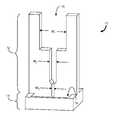
- FIG. 1is an isometric view of an embodiment of a notch antenna element according to the invention.
- FIG. 2A and FIG. 2Billustrate a cross-sectional view and a top view, respectively, of a notch antenna element mounted to a printed circuit board according to an embodiment of the invention.
- FIG. 3A and FIG. 3Billustrate a top view and a bottom view, respectively, of the printed circuit board depicted in FIG. 2 .
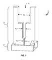
- FIG. 4illustrates a cross-sectional view of a notch antenna element mounted to a multi-layered printed circuit board according to another embodiment of the invention.
- FIG. 5illustrates a cross-sectional view of an embodiment of a two-dimensional multi-element step notch antenna array according to the invention.
- the inventionrelates to a notch antenna having a low profile stripline feed.
- Notch antenna elements fabricated from solid conductor materials and mounted on a printed circuit board (PCB) according to the inventionprovide superior heat dissipation when compared to conventional ESA antennas having vertical feeds.
- Thermally conductive viasi.e., “thermal vias” extending between the metallized surfaces of the PCB conduct heat generated by components surface mounted to the opposite side of the PCB from the notch antenna elements. Excess heat is removed by airflow passing over the antenna elements.
- system components and electrical routingcan be fabricated in a single PCB structure.
- conventional ESA antennasrequire mechanical connectors to couple the RF signals to or from each antenna element to other structures where the RF signals are distributed or processed.
- the total volume and weight of the ESA antenna of the inventionis substantially less than for a conventional ESA antenna.
- the notch antenna elementsare fabricated from lightweight nonconductive materials such as plastic and are coated with a conductive layer, making the ESA antenna advantageous for applications in which reduced weight is important.
- FIG. 1shows an isometric view of a notch antenna element 10 that can be used in an ESA antenna in accordance with the principles of the invention.
- the antenna element 10is fabricated as a solid aluminum piece and includes a vertical section 12 and a base 14 having an opening, i.e., base cavity 16 .
- the vertical section 12includes a stepped notch 18 having three distinct widths W 1 , W 2 and W 3 (generally M).
- W 1 , W 2 and W 3generally M
- Various parameters, including the notch widths W and the dimensions of the base cavity 16are selected to achieve acceptable impedance matching over a wide bandwidth.
- the notch antenna element 10has different notch geometries.
- the element 10can have a flared notch, a tapered notch or a linearly varying notch width as is known in the art.
- the particular notch configuration employedmay be determined according to performance requirements and manufacturing considerations.
- the notch antenna element 10is mounted to a printed circuit board (PCB) 20 as shown in the cross-sectional view of FIG. 2A . Only the lower portion of the base 14 is illustrated.
- the PCB 20includes a dielectric substrate 22 such as Arlon Copper Clad217, CLTE-XT, Rogers 4000 series or equivalent.
- the upper and lower surfaces of the dielectric substrate 22are coated by conductive layers 24 and 26 , respectively (e.g., metallization layers).
- the conductive layers 24 and 26are thin (e.g., 0.0007 in. thickness) copper layers.
- the region between the two conductive layers 24 and 26 directly beneath the base 14includes a number of electrically conductive vias 28 (shown as dashed lines as these vias do not lie in the cross-sectional plane of the figure).
- the electrically conductive vias 28are arranged along a perimeter bounding a cavity region in the dielectric substrate 22 .
- the perimeterhas lateral dimensions approximately equal to the lateral dimensions of the base cavity 16 .
- An electrically conductive RF signal via 30conducts an RF signal to be coupled to the notch antenna element 10 .
- the RF via 30passes vertically through an opening 32 in the lower conductive layer 26 and extends through most of the thickness t of the dielectric substrate 22 .
- a stripline 32extends horizontally from the top of the RF via 30 and is separated from the upper conductive layer 24 by a non-zero distance (e.g., 0.005 in.).
- the stripline 32has a length that is perpendicular to the slot 18 at the base 14 of the notch antenna element 10 and is electrically coupled to the upper conductive layer 24 at one end through a short vertical conductive segment 34 .
- the upper conductive layer 24includes an opening 38 beneath the slot 18 .
- a thin conductive layer 36(e.g., 0.0007 in. thick copper) is embedded in the dielectric substrate 22 and separated from the lower conductive layer 26 by a non-zero distance (e.g., 0.005 in.).
- FIG. 2Ba view of the upper surface of the PCB 20 as seen when looking down at a mounted notch antenna element 10 is shown.
- a small region of the upper conductive layer 24 and the upper surface of the dielectric substrate 22are visible as the base cavity is slightly larger and similarly shaped to the opening 38 .
- the length of the feed end of the slot 18is oriented vertically in the figure.
- FIG. 3Ashows a view of the upper conductive layer 24 with the opening 38 .
- the stripline 32is shown as a dashed linear feature that is embedded behind the upper conductive layer 24 , that is, in the dielectric substrate at a non-zero distance from the upper conductive layer 24 .
- FIG. 3Ba view looking up at the lower conductive layer 26 is shown.
- a stripline 40 extending laterally from the bottom of the RF via 30is separated from the lower conductive layer 26 by an opening 42 . Dashed circles illustrate the locations of the electrically conductive vias 28 that extend between the upper conductive layer 24 and the lower conductive layer 26 through the dielectric substrate 22 .
- FIG. 4shows a cross-sectional view of an embodiment of a notch antenna element mounted to a multi-layered PCB 46 in accordance with principles of the invention.
- the PCB 46includes multiple dielectric layers 48 A to 48 E (generally 48 ), an upper conductive layer 24 , four intermediate conductive layers 50 A to 50 D (generally 50 ), an embedded conductive layer 36 and a lower conductive layer 26 .
- the number of dielectric layers 48 and the number of intermediate conductive layers 50can be different.
- a number of electrically conductive vias 52extend vertically between the upper and lower conductive layers 24 and 26 .
- An RF via 54extends vertically through the upper three dielectric layers 48 A to 48 C to a distribution stripline 56 (only a small portion is visible) that extends horizontally within an opening in the third intermediate conductive layer 50 C in a manner similar to that shown for the stripline 40 of FIG. 3B .
- the distribution stripline 56conducts an RF signal between one or more locations or embedded components on the same layer of the multilayer PCB 46 and the notch antenna element.
- Embedded componentscan include distribution components, resistive elements, Wilkinson power dividers and hybrid couplers that are embedded in the dielectric layer 48 C or 48 D on the thin film distribution stripline 56 .
- the distribution stripline 56can be routed to an edge connector or other electrical coupling element attached to the PCB 46 to provide an efficient external connection.
- the external connectionmay be configured to receive an RF signal to be transmitted from the antenna element or to provide an RF signal received at the antenna element.
- Such signalsmay be processed in various manners by components disposed between the antenna element and the external connector.
- the RF via 54extends through the PCB 46 to a transmission line in the lower conductive layer 26 .
- larger componentsmay be surface mounted to the bottom of the PCB 46 and electrically coupled to other layers 50 or directly to the antenna element by RF vias 54 .
- Surface mounted componentscan generate significant heat therefore in some embodiments thermal vias are provided between the upper and lower conductive layers 24 and 26 .
- Thermal viaspass through the PCB 46 at locations that do not interfere with notch antenna elements, striplines and embedded and mounted components. Consequently, the thermal vias can have lateral dimensions (e.g., diameters) substantially greater than the dimensions of the RF vias 54 .
- the dimensions of the thermal viasmay be selected according to the desired thermal transfer capability to maintain required operational temperatures of the mounted components.
- FIG. 5illustrates a cross-sectional view of an embodiment of a two-dimensional multi-element step notch antenna array 60 according to the invention.
- the ESA antenna 60includes multiple rows of notch antenna elements 10 mounted to a multi-layer PCB 46 . Only five notch antenna elements 10 in a single row are illustrated for clarity.
- Each antenna element 10is mounted above a respective stripline and opening in the upper conductive surface as described above.
- electronic componentssuch as phase shifters, low noise amplifiers and mixers used in receiver mode operation, and attenuators and power amplifiers used for transmit mode operation are mounted on the lower conductive surface.
- componentscan be embedded in or between dielectric layers.
- antenna elements 10 fabricated as solid metal structurescan act as efficient heat sinks to remove excess heat generated by power amplifiers and other components.
Landscapes
- Waveguide Aerials (AREA)
- Details Of Aerials (AREA)
Abstract
Description
Claims (8)
Priority Applications (1)
| Application Number | Priority Date | Filing Date | Title |
|---|---|---|---|
| US12/126,418US8350767B2 (en) | 2007-05-30 | 2008-05-23 | Notch antenna having a low profile stripline feed |
Applications Claiming Priority (2)
| Application Number | Priority Date | Filing Date | Title |
|---|---|---|---|
| US94073907P | 2007-05-30 | 2007-05-30 | |
| US12/126,418US8350767B2 (en) | 2007-05-30 | 2008-05-23 | Notch antenna having a low profile stripline feed |
Publications (2)
| Publication Number | Publication Date |
|---|---|
| US20090322636A1 US20090322636A1 (en) | 2009-12-31 |
| US8350767B2true US8350767B2 (en) | 2013-01-08 |
Family
ID=40226748
Family Applications (1)
| Application Number | Title | Priority Date | Filing Date |
|---|---|---|---|
| US12/126,418Expired - Fee RelatedUS8350767B2 (en) | 2007-05-30 | 2008-05-23 | Notch antenna having a low profile stripline feed |
Country Status (2)
| Country | Link |
|---|---|
| US (1) | US8350767B2 (en) |
| WO (1) | WO2009005912A2 (en) |
Cited By (6)
| Publication number | Priority date | Publication date | Assignee | Title |
|---|---|---|---|---|
| US20190067823A1 (en)* | 2017-08-28 | 2019-02-28 | Raytheon Company | Surface mounted notch radiator with folded balun |
| US10541467B1 (en) | 2016-02-23 | 2020-01-21 | Massachusetts Institute Of Technology | Integrated coaxial notch antenna feed |
| US10833423B2 (en) | 2019-02-28 | 2020-11-10 | Massachusetts Institute Of Technology | Dual polarized notch antenna having low profile stripline feed |
| US10950929B2 (en)* | 2016-07-14 | 2021-03-16 | Massachusetts Institute Of Technology | Foam radiator |
| US10971824B2 (en)* | 2016-09-30 | 2021-04-06 | Ims Connector Systems Gmbh | Antenna element |
| US11476557B1 (en) | 2021-08-06 | 2022-10-18 | United States Of America As Represented By The Secretary Of The Navy | Dual-polarization heat-dissipating antenna array element |
Families Citing this family (23)
| Publication number | Priority date | Publication date | Assignee | Title |
|---|---|---|---|---|
| US8989837B2 (en) | 2009-12-01 | 2015-03-24 | Kyma Medical Technologies Ltd. | Methods and systems for determining fluid content of tissue |
| US9265438B2 (en) | 2008-05-27 | 2016-02-23 | Kyma Medical Technologies Ltd. | Locating features in the heart using radio frequency imaging |
| US9220420B2 (en) | 2010-07-21 | 2015-12-29 | Kyma Medical Technologies Ltd. | Implantable dielectrometer |
| US8860619B2 (en)* | 2011-09-20 | 2014-10-14 | Netgear, Inc. | Wireless device and multi-antenna system having dual open-slot radiators |
| US9093745B2 (en) | 2012-05-10 | 2015-07-28 | Apple Inc. | Antenna and proximity sensor structures having printed circuit and dielectric carrier layers |
| US9685707B2 (en)* | 2012-05-30 | 2017-06-20 | Raytheon Company | Active electronically scanned array antenna |
| US9635761B2 (en)* | 2013-07-15 | 2017-04-25 | Massachusetts Institute Of Technology | Sleeved coaxial printed circuit board vias |
| US10680324B2 (en)* | 2013-10-29 | 2020-06-09 | Zoll Medical Israel Ltd. | Antenna systems and devices and methods of manufacture thereof |
| KR102054200B1 (en)* | 2013-11-20 | 2020-01-23 | 삼성전자주식회사 | Microstrip patch antenna with cavity-backed structure including via-hole |
| US11013420B2 (en) | 2014-02-05 | 2021-05-25 | Zoll Medical Israel Ltd. | Systems, apparatuses and methods for determining blood pressure |
| US9958707B2 (en) | 2014-03-06 | 2018-05-01 | California Institute Of Technology | Systems and methods for implementing electrically tunable metasurfaces |
| US10249943B2 (en) | 2014-06-18 | 2019-04-02 | Massachusetts Institute Of Technology | Printed circuit board assembly with foam dielectric material |
| US9876283B2 (en) | 2014-06-19 | 2018-01-23 | Raytheon Company | Active electronically scanned array antenna |
| US11259715B2 (en) | 2014-09-08 | 2022-03-01 | Zoll Medical Israel Ltd. | Monitoring and diagnostics systems and methods |
| US10548485B2 (en) | 2015-01-12 | 2020-02-04 | Zoll Medical Israel Ltd. | Systems, apparatuses and methods for radio frequency-based attachment sensing |
| US9997827B2 (en) | 2016-03-03 | 2018-06-12 | Raytheon Company | Wideband array antenna and manufacturing methods |
| JP6747591B2 (en)* | 2017-05-30 | 2020-08-26 | 日立金属株式会社 | Planar array antenna and wireless communication module |
| US11020002B2 (en) | 2017-08-10 | 2021-06-01 | Zoll Medical Israel Ltd. | Systems, devices and methods for physiological monitoring of patients |
| WO2020176104A1 (en)* | 2019-02-28 | 2020-09-03 | Massachusetts Institute Of Technology | Dual polarized notch antenna having low profile stripline feed |
| EP3981045B1 (en)* | 2019-06-05 | 2025-05-07 | Ovzon Sweden AB | Antenna array |
| CN110676555B (en)* | 2019-10-22 | 2020-11-10 | 上海交通大学 | A heat sink antenna array structure |
| WO2022045947A1 (en)* | 2020-08-25 | 2022-03-03 | Saab Ab | A notch antenna structure |
| CN115473034A (en)* | 2022-09-19 | 2022-12-13 | 中国电子科技集团公司第十四研究所 | Metal slot line antenna based on strip line gap coupling |
Citations (16)
| Publication number | Priority date | Publication date | Assignee | Title |
|---|---|---|---|---|
| US5142255A (en)* | 1990-05-07 | 1992-08-25 | The Texas A&M University System | Planar active endfire radiating elements and coplanar waveguide filters with wide electronic tuning bandwidth |
| US5175560A (en) | 1991-03-25 | 1992-12-29 | Westinghouse Electric Corp. | Notch radiator elements |
| US5488380A (en) | 1991-05-24 | 1996-01-30 | The Boeing Company | Packaging architecture for phased arrays |
| US5949383A (en)* | 1997-10-20 | 1999-09-07 | Ericsson Inc. | Compact antenna structures including baluns |
| US6424313B1 (en) | 2000-08-29 | 2002-07-23 | The Boeing Company | Three dimensional packaging architecture for phased array antenna elements |
| US6621469B2 (en)* | 1999-04-26 | 2003-09-16 | Andrew Corporation | Transmit/receive distributed antenna systems |
| US6670930B2 (en)* | 2001-12-05 | 2003-12-30 | The Boeing Company | Antenna-integrated printed wiring board assembly for a phased array antenna system |
| US6963312B2 (en)* | 2001-09-04 | 2005-11-08 | Raytheon Company | Slot for decade band tapered slot antenna, and method of making and configuring same |
| US20060033207A1 (en)* | 2003-12-04 | 2006-02-16 | Sharp Kabushiki Kaisha | Microwave-monolithic-integrated-circuit-mounted substrate, transmitter device for transmission only and transceiver device for transmission/reception in microwave-band communication |
| US20060145927A1 (en)* | 2004-12-08 | 2006-07-06 | Won-Kyu Choi | PIFA and RFID tag using the same |
| US7095373B2 (en)* | 2004-05-25 | 2006-08-22 | Saga University | Planar array antenna |
| US20060273972A1 (en) | 2005-06-02 | 2006-12-07 | Chandler Cole A | Millimeter wave electronically scanned antenna |
| US20060290584A1 (en)* | 2005-06-22 | 2006-12-28 | Northrop Grumman Corporation | Hexagonal dual-pol notch array architecture having a triangular grid and concentric phase centers |
| US7180457B2 (en) | 2003-07-11 | 2007-02-20 | Raytheon Company | Wideband phased array radiator |
| US7417598B2 (en)* | 2006-11-08 | 2008-08-26 | The Boeing Company | Compact, low profile electronically scanned antenna |
| US7884768B2 (en)* | 2006-11-08 | 2011-02-08 | The Boeing Company | Compact, dual-beam phased array antenna architecture |
- 2008
- 2008-05-23USUS12/126,418patent/US8350767B2/ennot_activeExpired - Fee Related
- 2008-05-23WOPCT/US2008/064729patent/WO2009005912A2/enactiveApplication Filing
Patent Citations (16)
| Publication number | Priority date | Publication date | Assignee | Title |
|---|---|---|---|---|
| US5142255A (en)* | 1990-05-07 | 1992-08-25 | The Texas A&M University System | Planar active endfire radiating elements and coplanar waveguide filters with wide electronic tuning bandwidth |
| US5175560A (en) | 1991-03-25 | 1992-12-29 | Westinghouse Electric Corp. | Notch radiator elements |
| US5488380A (en) | 1991-05-24 | 1996-01-30 | The Boeing Company | Packaging architecture for phased arrays |
| US5949383A (en)* | 1997-10-20 | 1999-09-07 | Ericsson Inc. | Compact antenna structures including baluns |
| US6621469B2 (en)* | 1999-04-26 | 2003-09-16 | Andrew Corporation | Transmit/receive distributed antenna systems |
| US6424313B1 (en) | 2000-08-29 | 2002-07-23 | The Boeing Company | Three dimensional packaging architecture for phased array antenna elements |
| US6963312B2 (en)* | 2001-09-04 | 2005-11-08 | Raytheon Company | Slot for decade band tapered slot antenna, and method of making and configuring same |
| US6670930B2 (en)* | 2001-12-05 | 2003-12-30 | The Boeing Company | Antenna-integrated printed wiring board assembly for a phased array antenna system |
| US7180457B2 (en) | 2003-07-11 | 2007-02-20 | Raytheon Company | Wideband phased array radiator |
| US20060033207A1 (en)* | 2003-12-04 | 2006-02-16 | Sharp Kabushiki Kaisha | Microwave-monolithic-integrated-circuit-mounted substrate, transmitter device for transmission only and transceiver device for transmission/reception in microwave-band communication |
| US7095373B2 (en)* | 2004-05-25 | 2006-08-22 | Saga University | Planar array antenna |
| US20060145927A1 (en)* | 2004-12-08 | 2006-07-06 | Won-Kyu Choi | PIFA and RFID tag using the same |
| US20060273972A1 (en) | 2005-06-02 | 2006-12-07 | Chandler Cole A | Millimeter wave electronically scanned antenna |
| US20060290584A1 (en)* | 2005-06-22 | 2006-12-28 | Northrop Grumman Corporation | Hexagonal dual-pol notch array architecture having a triangular grid and concentric phase centers |
| US7417598B2 (en)* | 2006-11-08 | 2008-08-26 | The Boeing Company | Compact, low profile electronically scanned antenna |
| US7884768B2 (en)* | 2006-11-08 | 2011-02-08 | The Boeing Company | Compact, dual-beam phased array antenna architecture |
Non-Patent Citations (6)
| Title |
|---|
| "The Terminated Lossless Transmission Line," Microwave Engineering, Third Edition, David M. Pozar, pp. 57 to 64.* |
| Eric L. Holzman, "A Wide Band TEM Horn Array Radiator with a Novel Microstrip Feed", 2000 IEEE International Conference on Phased Array Systems and Technology. 2000. Proceedings., May 21-25, 2000, pp. 441-444. |
| International Search Report for corresponding PCT Appl. No. PCT/US08/64729 dated Dec. 12, 2008 (3 pgs). |
| K. Sigfrid Yngvesson, "Endfire Tapered Slot Antennas on Dielectric Substrates", IEEE Transactions on Antennas and Propagation, vol. AP-33, No. 12, Dec. 1985. |
| Raymond Tang, "Array Technology", Proceedings of the IEEE, vol. 80, No. 1, Jan. 1992. |
| Robert J. Mailloux, "Antenna Array Technology", Proceedings of the IEEE, vol. 80, No. 1, Jan. 1992. |
Cited By (8)
| Publication number | Priority date | Publication date | Assignee | Title |
|---|---|---|---|---|
| US10541467B1 (en) | 2016-02-23 | 2020-01-21 | Massachusetts Institute Of Technology | Integrated coaxial notch antenna feed |
| US10950929B2 (en)* | 2016-07-14 | 2021-03-16 | Massachusetts Institute Of Technology | Foam radiator |
| US10971824B2 (en)* | 2016-09-30 | 2021-04-06 | Ims Connector Systems Gmbh | Antenna element |
| US20190067823A1 (en)* | 2017-08-28 | 2019-02-28 | Raytheon Company | Surface mounted notch radiator with folded balun |
| WO2019045884A1 (en)* | 2017-08-28 | 2019-03-07 | Raytheon Company | Surface mounted notch radiator with folded balun |
| US10826186B2 (en)* | 2017-08-28 | 2020-11-03 | Raytheon Company | Surface mounted notch radiator with folded balun |
| US10833423B2 (en) | 2019-02-28 | 2020-11-10 | Massachusetts Institute Of Technology | Dual polarized notch antenna having low profile stripline feed |
| US11476557B1 (en) | 2021-08-06 | 2022-10-18 | United States Of America As Represented By The Secretary Of The Navy | Dual-polarization heat-dissipating antenna array element |
Also Published As
| Publication number | Publication date |
|---|---|
| WO2009005912A3 (en) | 2009-02-19 |
| US20090322636A1 (en) | 2009-12-31 |
| WO2009005912A2 (en) | 2009-01-08 |
Similar Documents
| Publication | Publication Date | Title |
|---|---|---|
| US8350767B2 (en) | Notch antenna having a low profile stripline feed | |
| Cheng et al. | W-band large-scale high-gain planar integrated antenna array | |
| US10749276B2 (en) | Spatial power-combining devices and antenna assemblies | |
| US9000996B2 (en) | Modular wideband antenna array | |
| AU2002334695B2 (en) | Slot coupled, polarized radiator | |
| US7446710B2 (en) | Integrated LTCC mm-wave planar array antenna with low loss feeding network | |
| US7187342B2 (en) | Antenna apparatus and method | |
| US5519408A (en) | Tapered notch antenna using coplanar waveguide | |
| US9402301B2 (en) | Vertical radio frequency module | |
| US9225070B1 (en) | Cavity backed aperture coupled dielectrically loaded waveguide radiating element with even mode excitation and wide angle impedance matching | |
| CA2594683C (en) | Array antenna including a monolithic antenna feed assembly and related methods | |
| US7324060B2 (en) | Power divider having unequal power division and antenna array feed network using such unequal power dividers | |
| US7436361B1 (en) | Low-loss dual polarized antenna for satcom and polarimetric weather radar | |
| EP1148583A1 (en) | Planar array antenna | |
| AU2002334695A1 (en) | Slot coupled, polarized radiator | |
| US20130082893A1 (en) | Co-phased, dual polarized antenna array with broadband and wide scan capability | |
| CN101277139A (en) | Broadband beam steering antenna | |
| WO2015135153A1 (en) | Array antenna | |
| CN110957574B (en) | A stripline-fed broadband millimeter-wave antenna unit | |
| CN114784489A (en) | Waveguide antenna assembly, radar, terminal and preparation method of waveguide antenna assembly | |
| CN111262025A (en) | Integrated Substrate Gap Waveguide Beam Scanning Leaky Wave Antenna | |
| IL208928A (en) | Wide band long slot array antenna using simple balun-less feed elements | |
| CN114843772B (en) | A dual-frequency, dual-circularly polarized, high-isolation Fabry-Perot cavity MIMO antenna and its processing method | |
| CN211670320U (en) | ISGW (integrated signal ground wire) beam scanning leaky-wave antenna | |
| WO2022105567A1 (en) | Dielectrically loaded printed dipole antenna |
Legal Events
| Date | Code | Title | Description |
|---|---|---|---|
| AS | Assignment | Owner name:MASSACHUSETTS INSTITUTE OF TECHNOLOGY, MASSACHUSET Free format text:ASSIGNMENT OF ASSIGNORS INTEREST;ASSIGNORS:BRIGHAM, GLENN A;DUFFY, SEAN M;HERD, JEFFREY;REEL/FRAME:021049/0404 Effective date:20080519 | |
| FEPP | Fee payment procedure | Free format text:PAYOR NUMBER ASSIGNED (ORIGINAL EVENT CODE: ASPN); ENTITY STATUS OF PATENT OWNER: SMALL ENTITY | |
| STCF | Information on status: patent grant | Free format text:PATENTED CASE | |
| AS | Assignment | Owner name:MASSACHUSETTS INSTITUTE OF TECHNOLOGY, MASSACHUSET Free format text:ASSIGNMENT OF ASSIGNORS INTEREST;ASSIGNOR:DAVIDOVITZ, MARAT;REEL/FRAME:029744/0603 Effective date:20041123 | |
| FEPP | Fee payment procedure | Free format text:PATENT HOLDER CLAIMS MICRO ENTITY STATUS, ENTITY STATUS SET TO MICRO (ORIGINAL EVENT CODE: STOM); ENTITY STATUS OF PATENT OWNER: SMALL ENTITY | |
| FPAY | Fee payment | Year of fee payment:4 | |
| FEPP | Fee payment procedure | Free format text:ENTITY STATUS SET TO SMALL (ORIGINAL EVENT CODE: SMAL); ENTITY STATUS OF PATENT OWNER: SMALL ENTITY | |
| MAFP | Maintenance fee payment | Free format text:PAYMENT OF MAINTENANCE FEE, 8TH YR, SMALL ENTITY (ORIGINAL EVENT CODE: M2552); ENTITY STATUS OF PATENT OWNER: SMALL ENTITY Year of fee payment:8 | |
| FEPP | Fee payment procedure | Free format text:MAINTENANCE FEE REMINDER MAILED (ORIGINAL EVENT CODE: REM.); ENTITY STATUS OF PATENT OWNER: SMALL ENTITY | |
| LAPS | Lapse for failure to pay maintenance fees | Free format text:PATENT EXPIRED FOR FAILURE TO PAY MAINTENANCE FEES (ORIGINAL EVENT CODE: EXP.); ENTITY STATUS OF PATENT OWNER: SMALL ENTITY | |
| STCH | Information on status: patent discontinuation | Free format text:PATENT EXPIRED DUE TO NONPAYMENT OF MAINTENANCE FEES UNDER 37 CFR 1.362 | |
| FP | Lapsed due to failure to pay maintenance fee | Effective date:20250108 |