US8350703B2 - RFID tags and processes for producing RFID tags - Google Patents
RFID tags and processes for producing RFID tagsDownload PDFInfo
- Publication number
- US8350703B2 US8350703B2US12/987,995US98799511AUS8350703B2US 8350703 B2US8350703 B2US 8350703B2US 98799511 AUS98799511 AUS 98799511AUS 8350703 B2US8350703 B2US 8350703B2
- Authority
- US
- United States
- Prior art keywords
- rfid tag
- conductive element
- integrated circuit
- rfid
- substrate
- Prior art date
- Legal status (The legal status is an assumption and is not a legal conclusion. Google has not performed a legal analysis and makes no representation as to the accuracy of the status listed.)
- Expired - Fee Related, expires
Links
Images


Classifications
- G—PHYSICS
- G06—COMPUTING OR CALCULATING; COUNTING
- G06K—GRAPHICAL DATA READING; PRESENTATION OF DATA; RECORD CARRIERS; HANDLING RECORD CARRIERS
- G06K19/00—Record carriers for use with machines and with at least a part designed to carry digital markings
- G06K19/06—Record carriers for use with machines and with at least a part designed to carry digital markings characterised by the kind of the digital marking, e.g. shape, nature, code
- G06K19/067—Record carriers with conductive marks, printed circuits or semiconductor circuit elements, e.g. credit or identity cards also with resonating or responding marks without active components
- G06K19/07—Record carriers with conductive marks, printed circuits or semiconductor circuit elements, e.g. credit or identity cards also with resonating or responding marks without active components with integrated circuit chips
- G06K19/077—Constructional details, e.g. mounting of circuits in the carrier
- G06K19/07749—Constructional details, e.g. mounting of circuits in the carrier the record carrier being capable of non-contact communication, e.g. constructional details of the antenna of a non-contact smart card
- G—PHYSICS
- G06—COMPUTING OR CALCULATING; COUNTING
- G06K—GRAPHICAL DATA READING; PRESENTATION OF DATA; RECORD CARRIERS; HANDLING RECORD CARRIERS
- G06K19/00—Record carriers for use with machines and with at least a part designed to carry digital markings
- G06K19/02—Record carriers for use with machines and with at least a part designed to carry digital markings characterised by the selection of materials, e.g. to avoid wear during transport through the machine
- G06K19/027—Record carriers for use with machines and with at least a part designed to carry digital markings characterised by the selection of materials, e.g. to avoid wear during transport through the machine the material being suitable for use as a textile, e.g. woven-based RFID-like labels designed for attachment to laundry items
- G—PHYSICS
- G06—COMPUTING OR CALCULATING; COUNTING
- G06K—GRAPHICAL DATA READING; PRESENTATION OF DATA; RECORD CARRIERS; HANDLING RECORD CARRIERS
- G06K19/00—Record carriers for use with machines and with at least a part designed to carry digital markings
- G06K19/06—Record carriers for use with machines and with at least a part designed to carry digital markings characterised by the kind of the digital marking, e.g. shape, nature, code
- G06K19/067—Record carriers with conductive marks, printed circuits or semiconductor circuit elements, e.g. credit or identity cards also with resonating or responding marks without active components
- G06K19/07—Record carriers with conductive marks, printed circuits or semiconductor circuit elements, e.g. credit or identity cards also with resonating or responding marks without active components with integrated circuit chips
- G06K19/077—Constructional details, e.g. mounting of circuits in the carrier
- G06K19/0772—Physical layout of the record carrier
- G06K19/07722—Physical layout of the record carrier the record carrier being multilayered, e.g. laminated sheets
- G—PHYSICS
- G06—COMPUTING OR CALCULATING; COUNTING
- G06K—GRAPHICAL DATA READING; PRESENTATION OF DATA; RECORD CARRIERS; HANDLING RECORD CARRIERS
- G06K19/00—Record carriers for use with machines and with at least a part designed to carry digital markings
- G06K19/06—Record carriers for use with machines and with at least a part designed to carry digital markings characterised by the kind of the digital marking, e.g. shape, nature, code
- G06K19/067—Record carriers with conductive marks, printed circuits or semiconductor circuit elements, e.g. credit or identity cards also with resonating or responding marks without active components
- G06K19/07—Record carriers with conductive marks, printed circuits or semiconductor circuit elements, e.g. credit or identity cards also with resonating or responding marks without active components with integrated circuit chips
- G06K19/077—Constructional details, e.g. mounting of circuits in the carrier
- G06K19/07749—Constructional details, e.g. mounting of circuits in the carrier the record carrier being capable of non-contact communication, e.g. constructional details of the antenna of a non-contact smart card
- G06K19/07758—Constructional details, e.g. mounting of circuits in the carrier the record carrier being capable of non-contact communication, e.g. constructional details of the antenna of a non-contact smart card arrangements for adhering the record carrier to further objects or living beings, functioning as an identification tag
- H—ELECTRICITY
- H01—ELECTRIC ELEMENTS
- H01L—SEMICONDUCTOR DEVICES NOT COVERED BY CLASS H10
- H01L24/00—Arrangements for connecting or disconnecting semiconductor or solid-state bodies; Methods or apparatus related thereto
- H01L24/01—Means for bonding being attached to, or being formed on, the surface to be connected, e.g. chip-to-package, die-attach, "first-level" interconnects; Manufacturing methods related thereto
- H01L24/18—High density interconnect [HDI] connectors; Manufacturing methods related thereto
- H01L24/23—Structure, shape, material or disposition of the high density interconnect connectors after the connecting process
- H01L24/24—Structure, shape, material or disposition of the high density interconnect connectors after the connecting process of an individual high density interconnect connector
- H—ELECTRICITY
- H01—ELECTRIC ELEMENTS
- H01L—SEMICONDUCTOR DEVICES NOT COVERED BY CLASS H10
- H01L24/00—Arrangements for connecting or disconnecting semiconductor or solid-state bodies; Methods or apparatus related thereto
- H01L24/80—Methods for connecting semiconductor or other solid state bodies using means for bonding being attached to, or being formed on, the surface to be connected
- H01L24/82—Methods for connecting semiconductor or other solid state bodies using means for bonding being attached to, or being formed on, the surface to be connected by forming build-up interconnects at chip-level, e.g. for high density interconnects [HDI]
- D—TEXTILES; PAPER
- D10—INDEXING SCHEME ASSOCIATED WITH SUBLASSES OF SECTION D, RELATING TO TEXTILES
- D10B—INDEXING SCHEME ASSOCIATED WITH SUBLASSES OF SECTION D, RELATING TO TEXTILES
- D10B2401/00—Physical properties
- D10B2401/18—Physical properties including electronic components
- H—ELECTRICITY
- H01—ELECTRIC ELEMENTS
- H01L—SEMICONDUCTOR DEVICES NOT COVERED BY CLASS H10
- H01L2224/00—Indexing scheme for arrangements for connecting or disconnecting semiconductor or solid-state bodies and methods related thereto as covered by H01L24/00
- H01L2224/01—Means for bonding being attached to, or being formed on, the surface to be connected, e.g. chip-to-package, die-attach, "first-level" interconnects; Manufacturing methods related thereto
- H01L2224/18—High density interconnect [HDI] connectors; Manufacturing methods related thereto
- H01L2224/23—Structure, shape, material or disposition of the high density interconnect connectors after the connecting process
- H01L2224/24—Structure, shape, material or disposition of the high density interconnect connectors after the connecting process of an individual high density interconnect connector
- H01L2224/241—Disposition
- H01L2224/24151—Connecting between a semiconductor or solid-state body and an item not being a semiconductor or solid-state body, e.g. chip-to-substrate, chip-to-passive
- H01L2224/24221—Connecting between a semiconductor or solid-state body and an item not being a semiconductor or solid-state body, e.g. chip-to-substrate, chip-to-passive the body and the item being stacked
- H01L2224/24225—Connecting between a semiconductor or solid-state body and an item not being a semiconductor or solid-state body, e.g. chip-to-substrate, chip-to-passive the body and the item being stacked the item being non-metallic, e.g. insulating substrate with or without metallisation
- H01L2224/24227—Connecting between a semiconductor or solid-state body and an item not being a semiconductor or solid-state body, e.g. chip-to-substrate, chip-to-passive the body and the item being stacked the item being non-metallic, e.g. insulating substrate with or without metallisation the HDI interconnect not connecting to the same level of the item at which the semiconductor or solid-state body is mounted, e.g. the semiconductor or solid-state body being mounted in a cavity or on a protrusion of the item
- H—ELECTRICITY
- H01—ELECTRIC ELEMENTS
- H01L—SEMICONDUCTOR DEVICES NOT COVERED BY CLASS H10
- H01L2224/00—Indexing scheme for arrangements for connecting or disconnecting semiconductor or solid-state bodies and methods related thereto as covered by H01L24/00
- H01L2224/74—Apparatus for manufacturing arrangements for connecting or disconnecting semiconductor or solid-state bodies and for methods related thereto
- H01L2224/76—Apparatus for connecting with build-up interconnects
- H01L2224/7615—Means for depositing
- H01L2224/76151—Means for direct writing
- H01L2224/76155—Jetting means, e.g. ink jet
- H—ELECTRICITY
- H01—ELECTRIC ELEMENTS
- H01L—SEMICONDUCTOR DEVICES NOT COVERED BY CLASS H10
- H01L2224/00—Indexing scheme for arrangements for connecting or disconnecting semiconductor or solid-state bodies and methods related thereto as covered by H01L24/00
- H01L2224/80—Methods for connecting semiconductor or other solid state bodies using means for bonding being attached to, or being formed on, the surface to be connected
- H01L2224/82—Methods for connecting semiconductor or other solid state bodies using means for bonding being attached to, or being formed on, the surface to be connected by forming build-up interconnects at chip-level, e.g. for high density interconnects [HDI]
- H01L2224/82009—Pre-treatment of the connector or the bonding area
- H01L2224/8203—Reshaping, e.g. forming vias
- H01L2224/82035—Reshaping, e.g. forming vias by heating means
- H01L2224/82039—Reshaping, e.g. forming vias by heating means using a laser
- H—ELECTRICITY
- H01—ELECTRIC ELEMENTS
- H01L—SEMICONDUCTOR DEVICES NOT COVERED BY CLASS H10
- H01L2224/00—Indexing scheme for arrangements for connecting or disconnecting semiconductor or solid-state bodies and methods related thereto as covered by H01L24/00
- H01L2224/80—Methods for connecting semiconductor or other solid state bodies using means for bonding being attached to, or being formed on, the surface to be connected
- H01L2224/82—Methods for connecting semiconductor or other solid state bodies using means for bonding being attached to, or being formed on, the surface to be connected by forming build-up interconnects at chip-level, e.g. for high density interconnects [HDI]
- H01L2224/821—Forming a build-up interconnect
- H01L2224/82101—Forming a build-up interconnect by additive methods, e.g. direct writing
- H01L2224/82102—Forming a build-up interconnect by additive methods, e.g. direct writing using jetting, e.g. ink jet
- H—ELECTRICITY
- H01—ELECTRIC ELEMENTS
- H01L—SEMICONDUCTOR DEVICES NOT COVERED BY CLASS H10
- H01L2924/00—Indexing scheme for arrangements or methods for connecting or disconnecting semiconductor or solid-state bodies as covered by H01L24/00
- H01L2924/01—Chemical elements
- H01L2924/01004—Beryllium [Be]
- H—ELECTRICITY
- H01—ELECTRIC ELEMENTS
- H01L—SEMICONDUCTOR DEVICES NOT COVERED BY CLASS H10
- H01L2924/00—Indexing scheme for arrangements or methods for connecting or disconnecting semiconductor or solid-state bodies as covered by H01L24/00
- H01L2924/01—Chemical elements
- H01L2924/01005—Boron [B]
- H—ELECTRICITY
- H01—ELECTRIC ELEMENTS
- H01L—SEMICONDUCTOR DEVICES NOT COVERED BY CLASS H10
- H01L2924/00—Indexing scheme for arrangements or methods for connecting or disconnecting semiconductor or solid-state bodies as covered by H01L24/00
- H01L2924/01—Chemical elements
- H01L2924/01027—Cobalt [Co]
- H—ELECTRICITY
- H01—ELECTRIC ELEMENTS
- H01L—SEMICONDUCTOR DEVICES NOT COVERED BY CLASS H10
- H01L2924/00—Indexing scheme for arrangements or methods for connecting or disconnecting semiconductor or solid-state bodies as covered by H01L24/00
- H01L2924/01—Chemical elements
- H01L2924/01033—Arsenic [As]
- H—ELECTRICITY
- H01—ELECTRIC ELEMENTS
- H01L—SEMICONDUCTOR DEVICES NOT COVERED BY CLASS H10
- H01L2924/00—Indexing scheme for arrangements or methods for connecting or disconnecting semiconductor or solid-state bodies as covered by H01L24/00
- H01L2924/01—Chemical elements
- H01L2924/01047—Silver [Ag]
- H—ELECTRICITY
- H01—ELECTRIC ELEMENTS
- H01L—SEMICONDUCTOR DEVICES NOT COVERED BY CLASS H10
- H01L2924/00—Indexing scheme for arrangements or methods for connecting or disconnecting semiconductor or solid-state bodies as covered by H01L24/00
- H01L2924/01—Chemical elements
- H01L2924/01051—Antimony [Sb]
- H—ELECTRICITY
- H01—ELECTRIC ELEMENTS
- H01L—SEMICONDUCTOR DEVICES NOT COVERED BY CLASS H10
- H01L2924/00—Indexing scheme for arrangements or methods for connecting or disconnecting semiconductor or solid-state bodies as covered by H01L24/00
- H01L2924/01—Chemical elements
- H01L2924/01079—Gold [Au]
- H—ELECTRICITY
- H01—ELECTRIC ELEMENTS
- H01L—SEMICONDUCTOR DEVICES NOT COVERED BY CLASS H10
- H01L2924/00—Indexing scheme for arrangements or methods for connecting or disconnecting semiconductor or solid-state bodies as covered by H01L24/00
- H01L2924/01—Chemical elements
- H01L2924/01082—Lead [Pb]
- H—ELECTRICITY
- H01—ELECTRIC ELEMENTS
- H01L—SEMICONDUCTOR DEVICES NOT COVERED BY CLASS H10
- H01L2924/00—Indexing scheme for arrangements or methods for connecting or disconnecting semiconductor or solid-state bodies as covered by H01L24/00
- H01L2924/013—Alloys
- H01L2924/014—Solder alloys
- H—ELECTRICITY
- H01—ELECTRIC ELEMENTS
- H01L—SEMICONDUCTOR DEVICES NOT COVERED BY CLASS H10
- H01L2924/00—Indexing scheme for arrangements or methods for connecting or disconnecting semiconductor or solid-state bodies as covered by H01L24/00
- H01L2924/06—Polymers
- H01L2924/078—Adhesive characteristics other than chemical
- H01L2924/07802—Adhesive characteristics other than chemical not being an ohmic electrical conductor
- H—ELECTRICITY
- H01—ELECTRIC ELEMENTS
- H01L—SEMICONDUCTOR DEVICES NOT COVERED BY CLASS H10
- H01L2924/00—Indexing scheme for arrangements or methods for connecting or disconnecting semiconductor or solid-state bodies as covered by H01L24/00
- H01L2924/10—Details of semiconductor or other solid state devices to be connected
- H01L2924/11—Device type
- H01L2924/12—Passive devices, e.g. 2 terminal devices
- H01L2924/1204—Optical Diode
- H01L2924/12042—LASER
- H—ELECTRICITY
- H01—ELECTRIC ELEMENTS
- H01L—SEMICONDUCTOR DEVICES NOT COVERED BY CLASS H10
- H01L2924/00—Indexing scheme for arrangements or methods for connecting or disconnecting semiconductor or solid-state bodies as covered by H01L24/00
- H01L2924/10—Details of semiconductor or other solid state devices to be connected
- H01L2924/11—Device type
- H01L2924/14—Integrated circuits
- H—ELECTRICITY
- H01—ELECTRIC ELEMENTS
- H01L—SEMICONDUCTOR DEVICES NOT COVERED BY CLASS H10
- H01L2924/00—Indexing scheme for arrangements or methods for connecting or disconnecting semiconductor or solid-state bodies as covered by H01L24/00
- H01L2924/15—Details of package parts other than the semiconductor or other solid state devices to be connected
- H01L2924/151—Die mounting substrate
- H01L2924/1515—Shape
- H01L2924/15153—Shape the die mounting substrate comprising a recess for hosting the device
- H—ELECTRICITY
- H01—ELECTRIC ELEMENTS
- H01L—SEMICONDUCTOR DEVICES NOT COVERED BY CLASS H10
- H01L2924/00—Indexing scheme for arrangements or methods for connecting or disconnecting semiconductor or solid-state bodies as covered by H01L24/00
- H01L2924/15—Details of package parts other than the semiconductor or other solid state devices to be connected
- H01L2924/151—Die mounting substrate
- H01L2924/15165—Monolayer substrate
- H—ELECTRICITY
- H01—ELECTRIC ELEMENTS
- H01L—SEMICONDUCTOR DEVICES NOT COVERED BY CLASS H10
- H01L2924/00—Indexing scheme for arrangements or methods for connecting or disconnecting semiconductor or solid-state bodies as covered by H01L24/00
- H01L2924/19—Details of hybrid assemblies other than the semiconductor or other solid state devices to be connected
- H01L2924/1901—Structure
- H01L2924/1904—Component type
- H01L2924/19041—Component type being a capacitor
- H—ELECTRICITY
- H01—ELECTRIC ELEMENTS
- H01L—SEMICONDUCTOR DEVICES NOT COVERED BY CLASS H10
- H01L2924/00—Indexing scheme for arrangements or methods for connecting or disconnecting semiconductor or solid-state bodies as covered by H01L24/00
- H01L2924/19—Details of hybrid assemblies other than the semiconductor or other solid state devices to be connected
- H01L2924/1901—Structure
- H01L2924/1904—Component type
- H01L2924/19042—Component type being an inductor
- H—ELECTRICITY
- H01—ELECTRIC ELEMENTS
- H01L—SEMICONDUCTOR DEVICES NOT COVERED BY CLASS H10
- H01L2924/00—Indexing scheme for arrangements or methods for connecting or disconnecting semiconductor or solid-state bodies as covered by H01L24/00
- H01L2924/30—Technical effects
- H01L2924/301—Electrical effects
- H01L2924/3011—Impedance
- Y—GENERAL TAGGING OF NEW TECHNOLOGICAL DEVELOPMENTS; GENERAL TAGGING OF CROSS-SECTIONAL TECHNOLOGIES SPANNING OVER SEVERAL SECTIONS OF THE IPC; TECHNICAL SUBJECTS COVERED BY FORMER USPC CROSS-REFERENCE ART COLLECTIONS [XRACs] AND DIGESTS
- Y10—TECHNICAL SUBJECTS COVERED BY FORMER USPC
- Y10T—TECHNICAL SUBJECTS COVERED BY FORMER US CLASSIFICATION
- Y10T29/00—Metal working
- Y10T29/49—Method of mechanical manufacture
- Y10T29/49002—Electrical device making
- Y10T29/49016—Antenna or wave energy "plumbing" making
- Y10T29/49018—Antenna or wave energy "plumbing" making with other electrical component
- Y—GENERAL TAGGING OF NEW TECHNOLOGICAL DEVELOPMENTS; GENERAL TAGGING OF CROSS-SECTIONAL TECHNOLOGIES SPANNING OVER SEVERAL SECTIONS OF THE IPC; TECHNICAL SUBJECTS COVERED BY FORMER USPC CROSS-REFERENCE ART COLLECTIONS [XRACs] AND DIGESTS
- Y10—TECHNICAL SUBJECTS COVERED BY FORMER USPC
- Y10T—TECHNICAL SUBJECTS COVERED BY FORMER US CLASSIFICATION
- Y10T29/00—Metal working
- Y10T29/49—Method of mechanical manufacture
- Y10T29/49002—Electrical device making
- Y10T29/49117—Conductor or circuit manufacturing
- Y10T29/49124—On flat or curved insulated base, e.g., printed circuit, etc.
- Y10T29/49155—Manufacturing circuit on or in base
Definitions
- Embodiments of the present inventionrelate generally to the Radio Frequency Identification (RFID) devices or tags and methods of making RFID devices or tags.
- RFIDRadio Frequency Identification
- Radio frequency identification (RFID) tagsallow for the remote identification of objects through the use of radio waves.
- Certain embodiments of the present inventions described hereare aimed at improving the present state of RFID technology by lowering assembly cost, by providing new and useful form factors, or by enabling new applications of RFID. While the designs and processes described here can be used to form many types of electronic assemblies (e.g. sensors or arrays for antennas or other devices which are not RFID tags), they are particularly useful for RFID tags, where cost, size, and form factor are desirable elements.
- RFID tagsare expanding into many applications from small merchandises to large merchandises. It is desirable to have the RFID tags be made as small as possible and as flexible as possible to enable the effective incorporation of the RFID tags into various merchandises. Also, it is desirable to have the RFID tags to be made as least expensive as possible to allow for wide integration of the RFID tags to into various merchandises.
- the exemplary embodiments of the present inventionpertain to a Radio Frequency Identification (RFID) tag.
- RFID tagcomprises a flexible substrate and an integrated circuit embedded within the flexible substrate. The top surface of the integrated circuit is coplanar with the flexible substrate. At least one conductive element is formed on the flexible substrate. The conductive element is electrically connected to the integrated circuit. The conductive element serves as an antenna for the RFID tag.
- an RFID tagcomprises a flexible substrate and an integrated circuit embedded within the flexible substrate.
- the top surface of the integrated circuitis coplanar with the flexible substrate.
- the integrated circuitis embedded within the flexible substrate using a fluidic self assembly (FSA) process.
- a planarization layeris formed over the flexible substrate and the integrated circuit.
- At least one conductive elementis formed on the flexible substrate and is electrically connected to the integrated circuit through at least one via created in the planarization layer. The conductive element serves as an antenna for the RFID tag.
- an RFID tagcomprises a flexible substrate and an integrated circuit embedded within the flexible substrate.
- the integrated circuithas a top surface that is coplanar with the flexible substrate.
- the conductive elementsare formed on the flexible substrate and electrically connected to the integrated circuit.
- the conductive elementsalso serve as an antenna for the RFID tag.
- the conductive elementsare formed on a top surface and bottom surface of the substrate. An electrical connection is provided to connect the conductive element on the bottom surface to the integrated circuit.
- an RFID tagcomprises an RFID integrated circuit deposited in a flexible substrate.
- a first antenna layeris coupled to the RFID integrated circuit.
- a second antenna layeris coupled to the RFID integrated circuit.
- the first antenna layeris above the RFID integrated circuit and the second antenna layer is below the RFID integrated.
- the RFID integrated circuitis coupled to the first antenna layer at the top of the RFID integrated circuit.
- the RFID integrated circuitis coupled to the second antenna layer at the bottom of the RFID integrated circuit.
- Another aspect of the inventionpertains to a method of assembling blocks where alignment is not critical.
- the methodincludes combining blocks, each containing a functional component, with a fluid to form a slurry.
- the slurryis then dispensed over a substrate having receptor holes, each of which is designed to receive one of the blocks.
- the relative size of each hole and blockis such that each block is not axially aligned relative to a perimeter of the receptor holes.
- Each blockis configured to include a bottom contact pad and a top contact pad that allow the functional component of the block to interconnect to conductive elements formed on the substrate even when each block is not axially aligned relative to the perimeter of the receptor holes.
- FIGS. 1-2compare actual sizes of exemplary RFID filaments or threads made in accordance with embodiments of the present invention to a U.S. dime;
- FIGS. 3-4illustrate in details an exemplary embodiment of an RFID tag having the form of a thread or filament
- FIGS. 5A-5Cillustrate more examples of an RFID tag having a filament structure using NanoBlockTM ICs as integrated circuit (NanoBlockTM is a trademark of Alien Technology Corporation);
- FIG. 6illustrates a densely-packed array of filament RFID tags formed on a flexible or plastic sheet
- FIG. 7illustrates an exemplary embodiment of an RFID tag
- FIG. 8illustrates another exemplary embodiment of an RFID tag
- FIGS. 9A-9Billustrate an exemplary embodiment of an RFID tag with top and bottom conductors forming an inductive loop
- FIG. 10illustrates exemplary dimensions of an RFID tag made in accordance with embodiments of the present invention.
- FIG. 11illustrates an exemplary embodiment of an RFID tag that does not require precise alignment and orientation when being deposited into a substrate
- FIG. 12illustrates an exemplary embodiment of assembling RFID tags in accordance with some embodiments of the present invention
- FIGS. 13A-13Billustrate another exemplary embodiment of assembling RFID tags in accordance with some embodiments of the present invention
- FIGS. 14A-14Billustrate an exemplary embodiment of assembling RFID tags wherein an FSA process is used to assemble the NanoBlockTM devices 110 into the holes in the substrate assembly;
- FIG. 15illustrates an exemplary embodiment of an RFID tag formed on a substrate and exemplary locations where the RFID tag can be cut for singulation;
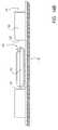
- FIG. 16illustrates a cross-sectional side view of singulated RFID tag
- FIG. 17illustrates exemplary cutting patterns for singulating RFID tags formed on a substrate
- FIG. 18illustrates a top-view and a cross-sectional view of a singulated RFID tag
- FIG. 19illustrates an RFID tag assembly that includes an inductor.
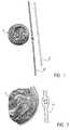
- FIGS. 1 and 2show photographic examples of electronic assemblies for RFID applications comparing the filament 10 and thread 20 of RFID to a U.S. dime.
- FIGS. 1 and 2show photographic examples of electronic assemblies for RFID applications comparing the filament 10 and thread 20 of RFID to a U.S. dime.
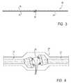
- an RFID tag 20comprises a flexible substrate 28 (in one embodiment, a plastic film), an integrated circuit 26 embedded within the flexible substrate 28 , and two conductive films 22 and 24 formed on top of the flexible or plastic substrate 28 .
- the conductive films 22 and 24are in electrical connection to the integrated circuit 26 that serve as antennas.
- FIG. 4shows a close up portion of the RFID tag 20 shown in FIG. 3 .
- the RFID tag 20includes a plurality of bonding pads 27 (or electrical connections) located on the integrated circuit (IC) 26 .
- the bonding padscan be placed around the center or the edges of the integrated circuit 26 , or at convenient locations on the integrated circuit.
- the two conductive films 22 and 24are connected to the integrated circuit 26 on opposite corners or in diagonal corners of the IC 26 .
- FIGS. 5A-5Cillustrate more examples of an RFID tag having a filament structure using a NanoBlockTM IC as an integrated circuit.
- NanoBlockTMis a trademark of Alien Technology Corporation. For clarity purposes, the printed conductors are not shown.
- FIGS. 5B-5Cshow the top and bottom view of the RFID tag.
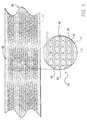
- a fluidic self assembly (FSA) processis used to form densely-packed array of filament tags on a flexible or plastic sheet.
- FSAis a process where a plurality of integrated circuit devices (such as NanoBlockTM ICs) are dispensed in a slurry. The slurry with the integrated circuits is dispensed over a substrate configured with receptors for the integrated circuits to be deposited therein. An example of this is shown in FIG. 6 . See U.S. Pat. No. 5,545,291 for a description of an FSA process.
- Each integrated circuitcan be a NanoBlockTM IC, which may be formed in the manner described in U.S. Patent Publication No. 2002/0127864-A1 and then placed into or on a receptor using an FSA process.
- FIG. 6is an illustration of one exemplary embodiment of a densely-packed array of filament tags on a substrate such as a plastic sheet 60 .
- a substratesuch as a plastic sheet 60 .
- Other substrate typesother than plastic can also be used.
- the substratecan have a form of a web substrate and is flexible.
- Each filament tagcan later be singulated to form an RFID tag.
- RFID integrated circuits 62are deposited in the plastic sheet 60 by FSA.
- Conductive traces 64are printed on at least one surface of the sheet to form antennas on the plastic sheet 60 .
- the conductive traces 64 that form the antennasare connected to the RFID integrated circuit 62 .
- the filament tagscan then be singulated to form individual RFID tags.
- An enlarged view 61shows an array of unsingulated filament tags on the plastic sheet 60 , where the array includes multiple RFID ICs 62 (deposited, through an FSA process, along lines formed by receptor locations on the plastic sheet which receive the RFID ICs) which are coupled to multiple conductive traces 64 .
- a singulation processis used to separate the array of tags into individual RFID tags; in one exemplary embodiment, the singulation process may be performed by mechanical cutting, sawing, punching, laser ablating, hot-blade knife cutting or other techniques.
- an individual RFID tagmay look like the RFID tag 20 shown in FIG. 3 . Exemplary dimensions of these tags produced from the plastic sheet 60 are described below and shown also in FIG. 10 . It can be seen from FIG. 6 that there are subarrays of RFID tags which are separated from each other by saw-tooth shaped gaps 63 .
- the ICs 62are deposited in lines which are parallel to the edges of the plastic sheet 60 which may be, in one exemplary embodiment, processed as a web material in a roll to roll web process, such as a type of process which is used to make paper.
- the printed conductive traces 64which are used to form the antenna elements for each tag, are formed at an oblique angle relative to the edges of the plastic sheet 60 . In the case of FIG. 6 , each conductive trace forms an angle of about 10°. This arrangement tends to optimize (e.g. maximize) the amount of filament RFID tags which can be fabricated in a given area of the plastic sheet 60 .
- the substrate containing the integrated circuitis made of plastic.
- the substratecan be made of other flexible materials as well.
- the thickness of the substrateis less than 1 mm, preferably less than 250 microns, and most preferably less than 125 microns.
- the width of the filament RFID tagis less than 5 mm, more preferably less than 3 mm, and could be less than 1 mm.
- the length of the RFID tag and the antenna formed on the RFID tag substratecan vary but should be at least 5 mm long, more preferably 10 mm long, and could even be as long as 100 mm. Thus, an RFID tag having this form factor will be long in length, thin in thickness and narrow in width.
- FIG. 10shows an example of the dimensions of the RFID tag filament relative to an IC, such as an RFID IC.
- the RFID tag assemblyis bonded to a nonconductive thread, and then woven into a fabric.
- the RFID tagcan be embedded in paper, with the flexible substrate of the RFID tag allowing the paper to remain flexible.
- the RFID tagcan be adhered to an adhesive material to allow it to attach to another item (e.g., clothing or other merchandise).
- the RFID tagSince the RFID tag is small, it can be hidden from view if desired.
- the RFID tagcould be hidden underneath an opaque surface.
- the RFID tagcan be colored black to make it difficult to see, or colored in a way as to blend in with its surroundings.
- the RFID tagcan be made black or be colored in such a way that makes the RFID tag matches the material that the RFID tag is incorporated into.
- a laminatemay be applied over the top surface (and/or the bottom surface) to protect the RFID tag from being cut out from the object into which it is embedded.
- the RFID tagcould be colored or metalized to stand out against its background in these applications. Thus, the RFID tag could have a distinct appearance that serves a purpose of authenticating the presences of the RFID tag.
- the RFID tagscan be used to authenticate or identify paper-based products, including currency, legal documents (e.g. a passport or a visa) or other valuable items.
- the thin size and flexibility characteristics of the RFID tagmake it possible to integrate the RFID tag into a label or tape, which can then be attached to an item to provide RFID tag capability.
- the RFID tagcan also be used to authenticate or identify non-paper items as well. For instance, the RFID tag's thin profile and small size make it easier to provide RFID tag capability to small, valuable items such as pharmaceuticals or electronic components.
- Such a tagcould be embedded within a container (such as embedded in a plastic container), or actually mixed in with the contents of a container.
- the RFID tagis deployed (or incorporated) or configured to deploy into another item in a way that the RFID tag spans into a three dimensional structure, e.g., an RFID thread bent into a curved RFID filament or thread or an RFID thread shaped or bent into a wrinkled RFID thread or otherwise an RFID tag shaped in a three dimensional structure.
- a three dimensional structuree.g., an RFID thread bent into a curved RFID filament or thread or an RFID thread shaped or bent into a wrinkled RFID thread or otherwise an RFID tag shaped in a three dimensional structure.
- FIG. 7shows, in a cross-sectional view, one construction of an RFID tag.
- An RFID tag shown in FIG. 7can be one of the RFID tag shown in FIG. 6 .
- an integrated circuit 71is deposited in a receptor hole 73 in the base film (a flexible or plastic substrate 75 ) using an FSA process.
- the integrated circuit 71is positioned or deposited such that it is coplanar with the flexible substrate 75 .
- coplanarrefers to a configuration where the integrated circuit 71 is deposited in the substrate 75 such that a surface of the integrated circuit 71 is flush with a surface of the substrate 75 .
- coplanarrefers to a configuration where the integrated circuit 71 is deposited in the substrate 75 such that a surface of the integrated circuit 71 is below a surface of the substrate 75 . In one embodiment, coplanar refers to a configuration where the integrated circuit 71 is deposited in the substrate 75 such that a top surface of the integrated circuit 71 shares essentially the same plane as the top surface of the substrate 75 .
- a planarization layer 77is formed on top of the substrate 75 and integrated circuit 71 . Via holes 72 are formed in the planarization layer to expose the contact pads (not shown) on the integrated circuit 71 .
- a metal interconnection 79(or metal traces) is then made to both provide a connection to the pads on the integrated circuit as well as to form antennas for the RFID tag. While photolithographic methods can be used to form the metal traces it is also possible to simply print conductive inks on the substrate 75 to form the antennas. This printing operation simultaneously forms an electrical connection to the integrated circuit 71 and forms the antenna elements.
- the RFID tag shown in FIG. 7may be similar to the tag 20 shown in FIG. 3 . It is to be noted that the RFID tag shown in FIG. 7 is not drawn to scale.
- a subtractive methodis used to form the antenna traces on the planarization layer.
- the subtractive methodincludes techniques such as chemical etching, laser ablation, and mechanical removal in which a continuous layer is first applied and then portions are etched away by chemical etching, laser ablation, or mechanical removal to create an appropriate pattern.
- an RFID tagis formed without a planarization layer.
- an integrated circuit 85is deposited in a receptor hole 73 in a substrate 83 (using an FSA process in one embodiment).
- a metal interconnection 81is formed directly on the top surface of the substrate 83 .
- No planarization layeris used in the RFID tag shown in FIG. 8 .
- the metal interconnection 81can be formed as a substantially continuous film over the substrate 83 and the integrated circuit 85 . An area (e.g., approximately in the center portion) on the integrated circuit 85 is left exposed.
- FIG. 9Ashows, in a cross-sectional view, another structure for an RFID filament (thread) tags, in which via holes 91 formed through a substrate 90 (e.g. a plastic substrate) provide access for electrical connection between a conductor 92 (e.g. an antenna element) formed on a top surface of the substrate 90 to a conductor 93 (e.g., an antenna element) formed on the bottom surface of the substrate 90 .
- a conductor 92e.g. an antenna element
- a conductor 93e.g., an antenna element
- the substrate 90includes an integrated circuit 94 which can be a NanoBlockTM IC.
- FIG. 9Adoes not show the presence of a top planarization layer, it should be recognized that it is possible to form an equivalent structure with a planarization layer as shown in FIG. 7 with via holes in the planarization layer and in the substrate to allow for electrical connection between the conductor on a top surface and a conductor on a bottom surface.
- FIG. 9Bshows a top view of the RFID tag of FIG. 9A .
- the IC 94is shown electrically connected to the conductors 92 formed on the top surface of the substrate 90 and to the conductor 93 formed on the bottom surface of the substrate 90 .
- the conductors 92 and 93may be printed on the substrate 90 or may be formed by other methods. In the example shown in FIG. 9B , the conductors 92 do not cover the entire top surface of the substrate 90 , and these conductors have been shown, for purposes of illustration, as transparent objects even though they may not be transparent.
- the conductor 93may or may not cover the entire bottom surface of the substrate 90 and may or may not be transparent.
- the via holes 91are shown adjacent the ends of the two top conductors 92 .
- the IC 94is coupled electrically to the conductors 92 through two bonding pads 94 A and 94 B on the IC 94 .
- the via holes 91may be created with laser ablation which drills through the plastic substrate.
- the top and bottom conductorsmay be electrically connected around the edges of the flexible substrate.
- One way of providing such a connectionis by coating or dipping the ends (or certain other portions which will not short circuit the IC) of the thread in a conductive ink.
- the electrical connection between the top and bottom conductorscan help prevent against damage to the IC 94 in the thread from electrostatic discharge and can also help to cancel reactance from the IC 94 .
- the RFID tag in FIG. 9Ahas the contact to the bottom conductor (through the via holes) configured or is used to match the impedance of the antenna elements and the RFID IC 94 .
- FIG. 10shows some illustrative dimensions for a filament RFID tag where the substrate which holds an IC 101 of the RFID tag is not shown.
- the substratemay be only minimally wider than the antenna elements 104 and 105 .
- the antenna elements 104 and 105are shown electrically coupled to the IC 101 through bonding pads 106 and 199 .
- the width of the RFID tagmay be equal to or slightly greater than the IC 101 (e.g. an RFID IC or a NanoBlockTM IC) contained within the RFID tag.
- the substratemay be slightly wider (e.g. about 0.10 mm or 0.20 mm wider) than the IC 101 or it may be substantially equal in width to the width of the IC 101 .
- the length of the RFID tagmay be at least 10 times the length of the IC 101 and more preferably may be at least 30 times the length of the IC 101 and could even be over 100 times the length of the IC 101 .
- the length of the RFID tagmay, in one embodiment, be optimized to cancel the electrical reactance of the RFID IC 101 in the RFID tag. Further, the structure of the antenna elements 104 and 105 may be designed to substantially or approximately match the impedance of the antenna elements to the input impedance of the RFID IC 101 .
- Exemplary RFID tags of the present inventioncan be formed from integrated circuits comprising two interconnection pads or more than two interconnection pads.
- RFID tags with three interconnection pads on the integrated circuit and RFID tags with four interconnection pads on the integrated circuitcan be used.
- one interconnection padserves as a local ground connection (which can still be attached to an antenna), one or more interconnection pads serve as an additional antenna connection, and one or more pads can be connected to an external capacitor or other electrical element to enhance the RFID tag performance.
- designs with 3 or 4 integrated circuit connection padscan be used in the designs and applications described herein.
- an RFID ICmay be created as a NanoBlockTM IC (e.g. using processes described in U.S. Patent Publication No. 2002/0127864-A1) or as a conventional IC (e.g. without the wedge-shaped sides of embodiments of a NanoBlockTM IC).
- FIG. 11illustrates an exemplary embodiment where an RFID IC can be assembled into a substrate where proper alignment or orientation of the RFID IC to be deposited into a receptor in the substrate is more relaxed or less stringent.
- an RFID IC 110is placed into a receptor 109 which includes a conductive element 117 that serves as an antenna element.
- the conductive element 117is thus located below the RFID IC 110 .
- This conductive element 117may be referred to as a bottom antenna and it is electrically coupled (resistively or capacitively) to the IC 110 .
- the RFID IC 110is also electrically coupled (resistively or capacitively) to a conductive element 107 which is above the RFID IC, and the conductive element 107 may be referred to as a top antenna.
- the RFID IC 110is electrically coupled to the top antenna through a contact 116 provided on a top surface of the RFID IC 110 and is electrically coupled to the bottom antenna through a contact 115 provided on a bottom surface of the RFID IC 110 .
- the IC bonding pads 137 and 136 on a top surface 114 of the IC 110make electrical contact, respectively, with a bottom contact 115 and a topside contact 116 .
- the bottom contact 115electrically connects with the bonding pad 137 and is wrapped around a side of the IC 110 (which resembles a block) and continues on the bottom side of the IC 110 .
- the IC 110is shown as having a wedge-shaped side but is will be appreciated that a rectangular-shaped side may also be used in certain embodiments.
- the size of the top contact 116 on a top surface of the RFID ICis significantly larger than a bonding pad 136 on the top of the RFID IC 110
- the size of the bottom contact 115 on the bottom surface of the RFIDis significantly larger than another bonding pad 137 on the top of the RFID IC 110
- the size of the top contact 116is about the same size as the entire top surface of the RFID IC 110
- the size of the bottom contact 115is about the same size as the entire bottom surface of the RFID IC 110 .
- the RFID IC 110includes an interconnect 115 a which extends from a bonding pad 137 on the top of the IC 110 , around a side of the IC 110 to the bottom of the IC 110 , and the bottom portion of this interconnect 115 a may be the bottom contact 115 .
- the RFID tagmay include a planarization layer or a dielectric layer (not shown) formed on top of the spacer layer 120 and the IC 110 similar to the RFID tag shown in FIG. 7 .
- the RFID IC 110is supported, in one embodiment, within a spacer layer 120 which is coupled to the top antenna 107 and to the bottom antenna 117 .
- the receptor or opening 109 in the spacer layer 120is considerably larger than the size of the RFID IC 110 .
- This opening 109is not designed to relatively precisely match the size of the block of the RFID IC 110 . Rather, the RFID IC 110 fits in the opening 109 without aligning to the perimeter of the opening 109 .
- the openingis at least 50% larger in area than the area of the bottom surface (or area of the top surface) of the block of the RFID IC 110 .
- the geometry of the opening 109does not need to match the geometry of the RFID IC 110 ; for example, the opening 109 may have a circular geometry and the RFID IC 110 may have a rectangular (e.g., square) geometry. Even though an FSA process may be used to place the RFID ICs 110 into the openings 109 , the RFID ICs 110 do not need to be aligned to the perimeter of the opening 109 . Thus, after an FSA process, the RFID ICs 110 may have different rotational orientations within the openings 109 .
- the RFID ICs 110 in this embodimentare designed to operate properly whether they are oriented up or down (relative to the layer of circuitry in the RFID IC 110 ) because there is only one electrical contact on a top surface of the RFID IC 110 (contact 116 ) and only one electrical contact on a bottom surface of the RFID IC 110 (contact 115 ). Since these contacts cover a large portion of both surfaces (top and bottom) of the RFID IC 110 and since there are no other electrical contacts on these surfaces, it is possible to deposit the RFID ICs 110 into the openings 109 without aligning them in the openings 109 and without needing to align small bonding pads on the RFID ICs 110 to interconnects on the top and bottom antennas.
- the embodiments discussedmay be used for thread tags or non-thread tags. These embodiments allow an FSA process in which blocks, each containing a functional element (e.g. an RFID IC), are mixed in a fluid to form a slurry and then the slurry is deposited onto a substrate having openings wherein the openings are substantially larger and/or having different shapes than the blocks and/or the perimeters of the blocks are not aligned with the perimeters of the openings after the FSA process is completed.
- a functional elemente.g. an RFID IC
- Exemplary methods for fabricating RFID thread tagsare detailed starting from pre-formed, two-terminal, RFID NanoBlockTM devices that have one electrical contact 116 located on the topside of the device and the other electrical contact 115 located on the bottom of the device.
- the methodsare amenable to implementation as a web based manufacturing process.
- an RFID NanoBlockTM device 110 with top and bottom electrical contacts 115 and 116 as shown in FIG. 11is provided.
- the electrical contacts 115 and 116may be formed from, or include a full or partial layer of, a conducting adhesive material, such as a silver-particle loaded thermal plastic or b-staged epoxy, low temperature solder, cold-weldable material such as gold, etc.
- a conducting adhesive materialsuch as a silver-particle loaded thermal plastic or b-staged epoxy, low temperature solder, cold-weldable material such as gold, etc.
- the electrical contacts 115 and 116may be covered by a thin layer of a non-conducting adhesive material, such as a PSA, hot-melt adhesive, etc, or non-conducting b-staged epoxy (in order to form, in one embodiment, a capacitive contact).
- the RFID NanoBlockTM device 110is deposited in a substrate to form an RFID tag.
- the RFID tagis formed on a web-base material or substrate and then singulated into an individual RFID tag.
- a plurality of RFID tagscan be formed on one substrate.
- FIG. 12illustrates an exemplary embodiment of assembling RFID tags in accordance with some embodiments of the present invention.
- an FSA processis used to assemble a plurality of RFID ICs into the substrate of the RFID tags.
- the spacer layer 120is adhered to a substrate that is a web-based material.
- a substrate 129 having one or more strips of a NanoBlockTM spacer layer 120 in which NanoBlockTM device receptor site holes 121 have been formedis provided.
- the substrate 129may have a form of a web substrate as shown in FIG. 12 .
- the cut-off end of the web substrateis to indicate that what is shown in the figure is a section from a long web (processed in a roll to roll web process, such as a paper making process).
- the holes 121have a circular shape. These circular holes 121 can be fabricated by punching, embossing, drilling, laser cutting or ablation, etc.
- the holes 121may have alternative geometries such as rectangular or square holes or have other regular shapes or even be irregularly shaped.
- the spacer layer 120may be coated on its front and/or back side with an adhesive material, such as a PSA, hot-melt adhesive, etc, or non-conducting b-staged epoxy or a UV-curable polymeric material (not shown).
- the thickness of this spacer layer 120 and the size of the holes 121are made such that no more than one NanoBlockTM device 110 will remain in each hole 121 after completion of the FSA process.
- the spacer layer 120 thicknesswould be selected to be approximately equal to the thickness of the NanoBlockTM devices 110 , and the hole diameter 121 could be in the range of 1.41 to 1.8 times the nominal NanoBlockTM device 110 width.
- a bottom-antenna layer 130is attached to the spacer layer 120 as illustrated in FIGS. 13A-13B .
- the bottom-antenna-layer 130is fabricated of a conducting material or is a layered structure that includes a conducting layer 131 .
- FIGS. 13A-13Bshow top and end-on views, respectively, of the bottom-antenna layer 130 .
- areas of one or both sides on the bottom-antenna-layer 130may be coated with an electrically conductive adhesive material (or non-conductive adhesive material in the case of a capacitive contact).
- the electrically conductive (or non-conductive) adhesive materialcan be applied by lamination or screen printing (or other suitable techniques) to the bottom-antenna-layer 130 .
- some areasincluding those that will contact either the top or bottom contacts of the NanoBlockTM devices 110 , may be coated with an electrically conductive adhesive such as the conducting adhesive strips 132 shown in FIGS. 13A and 13B (or a thin layer of a non-conducting adhesive in the case of a capacitive contact).
- the spacer layer 120(or a plurality of spacer layer strips 120 ) is attached to the bottom-antenna layer 130 by static pressure, lamination, etc., where one or more of the adhesive layers 132 discussed above bonds the pieces together.
- the spacer layer 120 and the bottom-antenna layer 130forms the substrate 129 for the RFID tag.
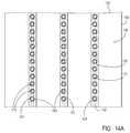
- an FSA processis used to assemble the NanoBlockTM devices 110 into the holes 121 in the substrate assembly.
- the ICs(such as NanoBlockTM devices 110 ) are mixed with a fluid to form a slurry and the slurry is dispensed over a substrate (such as bottom antenna layer 130 with layer 120 ), causing at least some of the ICs, shaped as blocks, to fall into and remain in the holes (e.g. holes 121 ) in the spacer layer 120 .
- FIGS. 14A and 14Bshow the result of an FSA process (or an alternative process) which was used to create the structure shown in these FIGS. 14A and 14B .
- the ICs 110are not axially aligned and are not rotationally aligned relative to their respective holes 121 ; thus, relative to the edge 133 , the ICs 110 have different rotational orientations and they also have, relative to their respective hole 121 , different axial positions within their respective hole 121 (e.g. some are positioned to the left of center, some are positioned to the right of center, etc.).
- the NanoBlockTM devices 110might now be attached to the substrate assembly by a hot-roll lamination process.
- the spacer layer 120is semi-transparent.
- the substrate assemblyincludes (as shown in FIG. 14A ) three strips of spacer layers 120 laminated onto a bottom antenna layer 130 . It is to be expected that more or less than three spacer layers 120 maybe included. In one embodiment, each strip of spacer layer 120 is aligned over one of the conducting adhesive strips 132 which are adhered onto the bottom antenna layer 130 .
- FIG. 14Bshows a close-up cross-section of a NanoBlockTM device 110 in a receptor site (hole 121 ) formed by an assembly of a strip of spacer layer (e.g. spacer layer 120 ) and the bottom antenna layer (e.g. layer 130 ).
- individual spacer layer strips 120are laminated over individual conducting adhesive strip 132 which is adhered on the bottom antenna layer 130 .
- the spacer layer strips 120are laminated over one continuous adhesive strip 132 .
- the adhesive layers 132 on the top and bottom of the spacer layer strip 120are employed to hold the assembly together, and the NanoBlockTM device 110 is held in place by a portion of the conducting adhesive strip 132 originally part of the bottom antenna layer 130 .
- a top antenna layer 135is laminated over the spacer layer 120 that has the RFID IC 110 deposited therein.
- the top antenna layer 135is fabricated of a conducting material or is a layered structure that includes a conducting layer 136 and has a structure, in one embodiment, which is similar to or the same as the structure of the bottom antenna layer 130 .
- the top antenna layer 135includes a conducting layer 136 , which may be supported on a plastic substrate (not shown) and conductive adhesive strips 132 adhered to the conducting layer 136 .
- the conductive adhesive strips 132 on the top antenna layermay be arranged in the same pattern as in the case of the bottom antenna layer (see, e.g. FIG. 14A ). With the presence of an adhesive layer that is conductive as the conductive adhesive strips 132 , the conducting layer 136 may be eliminated.
- top antenna layer 135may be coated with an electrically conductive or non-conductive adhesive material.
- some areas, including those that will contact either the top or bottom contact pads of the NanoBlockTM devices 110may be coated with an electrically conductive adhesive (e.g. conducting adhesive strips 132 ) or a thin layer of a non-conducting adhesive.
- the top antenna layer 135is laminated over the spacer layer 120 such that the conducting layer 136 makes electrical contact, resistive or capacitive, with any NanoBlockTM devices 110 present or deposited in the spacer layer 120 .
- the RFID tagsare formed on a web substrate.
- the web substrateincludes one or more spacer layer 120 each of which having receptors 121 for the RFID ICs 110 to be deposited therein. After the RFID ICs 110 are deposited and various layers laminated or formed as previously described, each individual RFID tag can be singulated from the web substrate.
- the web substrateis cut (e.g., in a web length-wise manner in order to separate sheets of connected RFID tags.
- FIG. 15illustrates two exemplary locations on the web substrate where an RFID tag formed can be singulated.
- FIG. 16illustrates an end-on view of a sheet that has an RFID tag singulated from the web substrate.
- the cutting operationmay be performed by mechanical cutting, sawing, punching, laser ablating, hot-blade knife cutting, gas-jet cutting, etc.
- FIG. 17illustrates a semi-transparent top-view of a sheet of connected RFID tags. On the left of the sheet is shown a bottom antenna layer 130 and on the right of the sheet is shown a top antenna layer 135 .
- a strip of spacer layer 120 having deposited therein a plurality of RFID IC 110is shown to be attached to the bottom-antenna layer 130 and the top-antenna layer 135 .
- Also shown in FIG. 17are two examples of how the RFID tags formed on a web substrate can be singulated.
- FIG. 18illustrates semi-transparent top-view and side view of a singulated or separated RFID tag cut using the cutting pattern A.
- the cutting operationmay be performed by mechanical cutting, sawing, punching, laser ablating, hot-blade knife cutting, gas jet cutting, etc. Cuts can be made straight across the sheets or in more complicated patterns in order to affect electrical characteristics of the resulting antenna or physical or design characteristics of the tags.
- holesmay also be formed in the antenna layers to affect form, function, and utility.
- FIG. 19An alternate tag assembly that includes an inductor in parallel with the NanoBlockTM device is shown in FIG. 19 .
- the RFID tagincludes one additional strip of conducting adhesive per spacer layer strip, applied to either the top or bottom antenna layer, and wide spacer layer strips.
- the inductor formedcan improve tag electrical performance.
- FIG. 19illustrates an end-on-view of an RFID tag in a sheet format.
- the RFID tagincludes a wide spacer layer 180 , an additional strip of conducting adhesive 183 , applied to either the bottom antenna layer 181 or top antenna layer 182 .
- the RFID tag assembly shown in FIG. 19is similar to the tag assembly shown in FIG. 15 and includes the bottom antenna layer 181 (which has a conducting layer which serves as the bottom antenna and a conducting adhesive strip which electrically connects the bottom antenna to the bottom contact on the RFID IC 110 ) and the top antenna layer 182 (which has a conducting layer which serves as the top antenna and a conducting adhesive strip which electrically connects the top antenna to the top contact on the IC 110 ) and a wide spacer layer 180 which includes an opening to receive the RFID IC 110 .
- the bottom antenna layer 181 and the top antenna layer 182are electrically joined along the added conducting adhesive 183 strip.
- the conduction path around the wide spacer layer 180forms an inductor loop in parallel with the RFID IC 110 (e.g., a NanoBlockTM device), thus enhancing electrical performance in certain embodiments.
Landscapes
- Engineering & Computer Science (AREA)
- Computer Hardware Design (AREA)
- Microelectronics & Electronic Packaging (AREA)
- Physics & Mathematics (AREA)
- General Physics & Mathematics (AREA)
- Theoretical Computer Science (AREA)
- Power Engineering (AREA)
- Textile Engineering (AREA)
- Details Of Aerials (AREA)
- Credit Cards Or The Like (AREA)
Abstract
Description
Claims (14)
Priority Applications (3)
| Application Number | Priority Date | Filing Date | Title |
|---|---|---|---|
| US12/987,995US8350703B2 (en) | 2003-03-24 | 2011-01-10 | RFID tags and processes for producing RFID tags |
| US13/730,105US8912907B2 (en) | 2003-03-24 | 2012-12-28 | RFID tags and processes for producing RFID tags |
| US14/559,695US9418328B2 (en) | 2003-03-24 | 2014-12-03 | RFID tags and processes for producing RFID tags |
Applications Claiming Priority (5)
| Application Number | Priority Date | Filing Date | Title |
|---|---|---|---|
| US45726303P | 2003-03-24 | 2003-03-24 | |
| US10/807,775US7253735B2 (en) | 2003-03-24 | 2004-03-23 | RFID tags and processes for producing RFID tags |
| US11/497,402US7489248B2 (en) | 2003-03-24 | 2006-07-31 | RFID tags and processes for producing RFID tags |
| US12/366,617US7868766B2 (en) | 2003-03-24 | 2009-02-05 | RFID tags and processes for producing RFID tags |
| US12/987,995US8350703B2 (en) | 2003-03-24 | 2011-01-10 | RFID tags and processes for producing RFID tags |
Related Parent Applications (2)
| Application Number | Title | Priority Date | Filing Date |
|---|---|---|---|
| US12/366,617DivisionUS7868766B2 (en) | 2003-03-24 | 2009-02-05 | RFID tags and processes for producing RFID tags |
| US12/366,617ContinuationUS7868766B2 (en) | 2003-03-24 | 2009-02-05 | RFID tags and processes for producing RFID tags |
Related Child Applications (1)
| Application Number | Title | Priority Date | Filing Date |
|---|---|---|---|
| US13/730,105ContinuationUS8912907B2 (en) | 2003-03-24 | 2012-12-28 | RFID tags and processes for producing RFID tags |
Publications (2)
| Publication Number | Publication Date |
|---|---|
| US20110186640A1 US20110186640A1 (en) | 2011-08-04 |
| US8350703B2true US8350703B2 (en) | 2013-01-08 |
Family
ID=32994822
Family Applications (6)
| Application Number | Title | Priority Date | Filing Date |
|---|---|---|---|
| US10/807,775Expired - Fee RelatedUS7253735B2 (en) | 2003-03-24 | 2004-03-23 | RFID tags and processes for producing RFID tags |
| US11/497,402Expired - Fee RelatedUS7489248B2 (en) | 2003-03-24 | 2006-07-31 | RFID tags and processes for producing RFID tags |
| US12/366,617Expired - LifetimeUS7868766B2 (en) | 2003-03-24 | 2009-02-05 | RFID tags and processes for producing RFID tags |
| US12/987,995Expired - Fee RelatedUS8350703B2 (en) | 2003-03-24 | 2011-01-10 | RFID tags and processes for producing RFID tags |
| US13/730,105Expired - LifetimeUS8912907B2 (en) | 2003-03-24 | 2012-12-28 | RFID tags and processes for producing RFID tags |
| US14/559,695Expired - Fee RelatedUS9418328B2 (en) | 2003-03-24 | 2014-12-03 | RFID tags and processes for producing RFID tags |
Family Applications Before (3)
| Application Number | Title | Priority Date | Filing Date |
|---|---|---|---|
| US10/807,775Expired - Fee RelatedUS7253735B2 (en) | 2003-03-24 | 2004-03-23 | RFID tags and processes for producing RFID tags |
| US11/497,402Expired - Fee RelatedUS7489248B2 (en) | 2003-03-24 | 2006-07-31 | RFID tags and processes for producing RFID tags |
| US12/366,617Expired - LifetimeUS7868766B2 (en) | 2003-03-24 | 2009-02-05 | RFID tags and processes for producing RFID tags |
Family Applications After (2)
| Application Number | Title | Priority Date | Filing Date |
|---|---|---|---|
| US13/730,105Expired - LifetimeUS8912907B2 (en) | 2003-03-24 | 2012-12-28 | RFID tags and processes for producing RFID tags |
| US14/559,695Expired - Fee RelatedUS9418328B2 (en) | 2003-03-24 | 2014-12-03 | RFID tags and processes for producing RFID tags |
Country Status (4)
| Country | Link |
|---|---|
| US (6) | US7253735B2 (en) |
| EP (1) | EP1606778A4 (en) |
| CN (1) | CN1764932B (en) |
| WO (1) | WO2004086289A2 (en) |
Cited By (4)
| Publication number | Priority date | Publication date | Assignee | Title |
|---|---|---|---|---|
| US20100187002A1 (en)* | 2009-01-29 | 2010-07-29 | Seung Seoup Lee | Method of attaching die using self-assembling monolayer and package substrate including die attached thereto using self-assembling monolayer |
| US20130000836A1 (en)* | 2011-07-01 | 2013-01-03 | Konica Minolta Business Technologies, Inc. | Production process of non-contact information recording medium |
| USD763833S1 (en) | 2014-10-01 | 2016-08-16 | Ohio State Innovation Foundation | RFID tag |
| US10685273B2 (en) | 2016-10-07 | 2020-06-16 | Avery Dennison Retail Information Services, Llc | Vibratory feeder systems for RFID elements |
Families Citing this family (204)
| Publication number | Priority date | Publication date | Assignee | Title |
|---|---|---|---|---|
| US6479395B1 (en)* | 1999-11-02 | 2002-11-12 | Alien Technology Corporation | Methods for forming openings in a substrate and apparatuses with these openings and methods for creating assemblies with openings |
| US6623579B1 (en)* | 1999-11-02 | 2003-09-23 | Alien Technology Corporation | Methods and apparatus for fluidic self assembly |
| US6951596B2 (en) | 2002-01-18 | 2005-10-04 | Avery Dennison Corporation | RFID label technique |
| US20030130912A1 (en) | 2002-01-04 | 2003-07-10 | Davis Tommy Lee | Equipment management system |
| US7224280B2 (en)* | 2002-12-31 | 2007-05-29 | Avery Dennison Corporation | RFID device and method of forming |
| JP3739752B2 (en) | 2003-02-07 | 2006-01-25 | 株式会社 ハリーズ | Small-piece transfer device capable of random-cycle shifting |
| US7253735B2 (en) | 2003-03-24 | 2007-08-07 | Alien Technology Corporation | RFID tags and processes for producing RFID tags |
| JP2005111973A (en)* | 2003-09-18 | 2005-04-28 | Konica Minolta Medical & Graphic Inc | Printing plate material, printing plate material roll, printing plate manufacturing method, printing method, and printing plate material manufacturing method |
| US7691009B2 (en)* | 2003-09-26 | 2010-04-06 | Radar Golf, Inc. | Apparatuses and methods relating to findable balls |
| US20080272885A1 (en)* | 2004-01-22 | 2008-11-06 | Mikoh Corporation | Modular Radio Frequency Identification Tagging Method |
| US7384496B2 (en)* | 2004-02-23 | 2008-06-10 | Checkpoint Systems, Inc. | Security tag system for fabricating a tag including an integrated surface processing system |
| US7019391B2 (en)* | 2004-04-06 | 2006-03-28 | Bao Tran | NANO IC packaging |
| KR100603761B1 (en)* | 2004-04-22 | 2006-07-24 | 삼성전자주식회사 | Microwave transponder |
| CN101427182B (en) | 2004-04-27 | 2011-10-19 | 伊利诺伊大学评议会 | Composite patterning equipment for soft lithography |
| US7268063B1 (en)* | 2004-06-01 | 2007-09-11 | University Of Central Florida | Process for fabricating semiconductor component |
| US8217381B2 (en) | 2004-06-04 | 2012-07-10 | The Board Of Trustees Of The University Of Illinois | Controlled buckling structures in semiconductor interconnects and nanomembranes for stretchable electronics |
| CN103646848B (en) | 2004-06-04 | 2018-06-05 | 伊利诺伊大学评议会 | The method of assembling printable semiconductor elements and manufacture electronic device |
| US7943491B2 (en) | 2004-06-04 | 2011-05-17 | The Board Of Trustees Of The University Of Illinois | Pattern transfer printing by kinetic control of adhesion to an elastomeric stamp |
| US7799699B2 (en) | 2004-06-04 | 2010-09-21 | The Board Of Trustees Of The University Of Illinois | Printable semiconductor structures and related methods of making and assembling |
| US7521292B2 (en) | 2004-06-04 | 2009-04-21 | The Board Of Trustees Of The University Of Illinois | Stretchable form of single crystal silicon for high performance electronics on rubber substrates |
| US20060020803A1 (en)* | 2004-07-06 | 2006-01-26 | Zih Corp. | Systems and methods for authentication of items or documents |
| US6957777B1 (en)* | 2004-09-21 | 2005-10-25 | Sheng-Chang Huang | Label to be attached on a plastic product formed in a mold and identifiable by a detecting device |
| US7500307B2 (en) | 2004-09-22 | 2009-03-10 | Avery Dennison Corporation | High-speed RFID circuit placement method |
| US7452748B1 (en) | 2004-11-08 | 2008-11-18 | Alien Technology Corporation | Strap assembly comprising functional block deposited therein and method of making same |
| AU2005322072A1 (en) | 2004-12-27 | 2006-07-06 | Quantum Paper, Inc. | Addressable and printable emissive display |
| US7712674B1 (en)* | 2005-02-22 | 2010-05-11 | Eigent Technologies Llc | RFID devices for verification of correctness, reliability, functionality and security |
| EP1851692A1 (en)* | 2005-02-23 | 2007-11-07 | Textilma Ag | Transponder-thread and application thereof |
| US7691280B2 (en)* | 2005-03-25 | 2010-04-06 | E. I. Du Pont De Nemours And Company | Ink jet printing of etchants and modifiers |
| US7623034B2 (en) | 2005-04-25 | 2009-11-24 | Avery Dennison Corporation | High-speed RFID circuit placement method and device |
| JP2008541441A (en)* | 2005-05-11 | 2008-11-20 | ストミクロエレクトロニクス・ソシエテ・アノニム | Silicon chip with inclined contact pads and electronic module comprising such a chip |
| JP4815891B2 (en)* | 2005-06-22 | 2011-11-16 | 株式会社日立製作所 | Wireless IC tag and antenna manufacturing method |
| US20060290498A1 (en)* | 2005-06-23 | 2006-12-28 | Ncr Corporation | Incorporation of RFID devices into labels |
| US7436305B2 (en)* | 2005-07-19 | 2008-10-14 | Checkpoint Systems, Inc. | RFID tags for pallets and cartons and system for attaching same |
| US7528727B2 (en)* | 2005-08-04 | 2009-05-05 | Sonoco Development, Inc. | Tracking device for polymeric packaging |
| US20070031992A1 (en)* | 2005-08-05 | 2007-02-08 | Schatz Kenneth D | Apparatuses and methods facilitating functional block deposition |
| WO2007025060A2 (en)* | 2005-08-25 | 2007-03-01 | Bae Systems Information And Electronics Systems Integration Inc. | Rfid tag and method and apparatus for manufacturing same |
| US7408463B2 (en) | 2005-09-30 | 2008-08-05 | Intel Corporation | Radio frequency identification tag |
| JP4896141B2 (en)* | 2005-10-06 | 2012-03-14 | テクスティルマ・アクチェンゲゼルシャフト | Narrow loom |
| US20070130754A1 (en)* | 2005-12-14 | 2007-06-14 | Michael Fein | Laser ablation prototyping of RFID antennas |
| US7555826B2 (en) | 2005-12-22 | 2009-07-07 | Avery Dennison Corporation | Method of manufacturing RFID devices |
| US8317107B2 (en)* | 2005-12-30 | 2012-11-27 | Intel Corporation | Chip-spacer integrated radio frequency ID tags, methods of making same, and systems containing same |
| US20070158804A1 (en)* | 2006-01-10 | 2007-07-12 | Semiconductor Energy Laboratory Co., Ltd. | Semiconductor device, manufacturing method of semiconductor device, and RFID tag |
| US20070159337A1 (en)* | 2006-01-12 | 2007-07-12 | Sdgi Holdings, Inc. | Modular RFID tag |
| EP1821241A3 (en)* | 2006-02-15 | 2008-07-23 | Assa Abloy AB | Hybrid frequency contactless transponder unit, module for and method of manufacturing |
| CA2655219A1 (en)* | 2006-07-24 | 2008-01-31 | Textilma Ag | Rfid tag |
| US7561107B2 (en) | 2006-09-07 | 2009-07-14 | Intelleflex Corporation | RFID device with microstrip antennas |
| US20080062046A1 (en)* | 2006-09-08 | 2008-03-13 | Intelleflex Corporation | Mounting structure for matching an rf integrated circuit with an antenna and rfid device implementing same |
| US10032102B2 (en) | 2006-10-31 | 2018-07-24 | Fiber Mountain, Inc. | Excess radio-frequency (RF) power storage in RF identification (RFID) tags, and related systems and methods |
| US8421626B2 (en)* | 2006-10-31 | 2013-04-16 | Corning Cable Systems, Llc | Radio frequency identification transponder for communicating condition of a component |
| US7772975B2 (en)* | 2006-10-31 | 2010-08-10 | Corning Cable Systems, Llc | System for mapping connections using RFID function |
| US9652708B2 (en) | 2006-10-31 | 2017-05-16 | Fiber Mountain, Inc. | Protocol for communications between a radio frequency identification (RFID) tag and a connected device, and related systems and methods |
| US7782202B2 (en) | 2006-10-31 | 2010-08-24 | Corning Cable Systems, Llc | Radio frequency identification of component connections |
| US9652709B2 (en) | 2006-10-31 | 2017-05-16 | Fiber Mountain, Inc. | Communications between multiple radio frequency identification (RFID) connected tags and one or more devices, and related systems and methods |
| US8264366B2 (en) | 2009-03-31 | 2012-09-11 | Corning Incorporated | Components, systems, and methods for associating sensor data with component location |
| US9652707B2 (en) | 2006-10-31 | 2017-05-16 | Fiber Mountain, Inc. | Radio frequency identification (RFID) connected tag communications protocol and related systems and methods |
| US8283683B2 (en) | 2006-11-07 | 2012-10-09 | Opto Tech Corporation | Chip-bonding light emitting diode chip |
| US20080106415A1 (en)* | 2006-11-08 | 2008-05-08 | Macsema, Inc. | Information tag |
| US7701352B2 (en)* | 2006-11-22 | 2010-04-20 | Avery Dennison Corporation | RFID label with release liner window, and method of making |
| US7667574B2 (en)* | 2006-12-14 | 2010-02-23 | Corning Cable Systems, Llc | Signal-processing systems and methods for RFID-tag signals |
| US7760094B1 (en) | 2006-12-14 | 2010-07-20 | Corning Cable Systems Llc | RFID systems and methods for optical fiber network deployment and maintenance |
| US8264355B2 (en) | 2006-12-14 | 2012-09-11 | Corning Cable Systems Llc | RFID systems and methods for optical fiber network deployment and maintenance |
| EP2104954B1 (en) | 2007-01-17 | 2022-03-16 | The Board of Trustees of the University of Illinois | Optical systems fabricated by printing-based assembly |
| US7893385B2 (en)* | 2007-03-01 | 2011-02-22 | James Neil Rodgers | Method for enhancing gain and range of an RFID antenna |
| US7547150B2 (en) | 2007-03-09 | 2009-06-16 | Corning Cable Systems, Llc | Optically addressed RFID elements |
| US7965186B2 (en) | 2007-03-09 | 2011-06-21 | Corning Cable Systems, Llc | Passive RFID elements having visual indicators |
| HK1109708A2 (en) | 2007-04-24 | 2008-06-13 | On Track Innovations Ltd. | Interface card and apparatus and process for the formation thereof |
| EP2000957A1 (en)* | 2007-05-21 | 2008-12-10 | Gemplus | Method of manufacturing a device comprising a radiofrequency transponder antenna with two terminal portions made on a single medium and device obtained |
| US8133768B2 (en) | 2007-05-31 | 2012-03-13 | Nthdegree Technologies Worldwide Inc | Method of manufacturing a light emitting, photovoltaic or other electronic apparatus and system |
| US8809126B2 (en) | 2007-05-31 | 2014-08-19 | Nthdegree Technologies Worldwide Inc | Printable composition of a liquid or gel suspension of diodes |
| US8852467B2 (en) | 2007-05-31 | 2014-10-07 | Nthdegree Technologies Worldwide Inc | Method of manufacturing a printable composition of a liquid or gel suspension of diodes |
| US8384630B2 (en) | 2007-05-31 | 2013-02-26 | Nthdegree Technologies Worldwide Inc | Light emitting, photovoltaic or other electronic apparatus and system |
| US9425357B2 (en) | 2007-05-31 | 2016-08-23 | Nthdegree Technologies Worldwide Inc. | Diode for a printable composition |
| US8889216B2 (en) | 2007-05-31 | 2014-11-18 | Nthdegree Technologies Worldwide Inc | Method of manufacturing addressable and static electronic displays |
| US9018833B2 (en) | 2007-05-31 | 2015-04-28 | Nthdegree Technologies Worldwide Inc | Apparatus with light emitting or absorbing diodes |
| US8415879B2 (en) | 2007-05-31 | 2013-04-09 | Nthdegree Technologies Worldwide Inc | Diode for a printable composition |
| US9419179B2 (en) | 2007-05-31 | 2016-08-16 | Nthdegree Technologies Worldwide Inc | Diode for a printable composition |
| US9343593B2 (en) | 2007-05-31 | 2016-05-17 | Nthdegree Technologies Worldwide Inc | Printable composition of a liquid or gel suspension of diodes |
| US8674593B2 (en) | 2007-05-31 | 2014-03-18 | Nthdegree Technologies Worldwide Inc | Diode for a printable composition |
| US8877101B2 (en) | 2007-05-31 | 2014-11-04 | Nthdegree Technologies Worldwide Inc | Method of manufacturing a light emitting, power generating or other electronic apparatus |
| US8846457B2 (en) | 2007-05-31 | 2014-09-30 | Nthdegree Technologies Worldwide Inc | Printable composition of a liquid or gel suspension of diodes |
| US9534772B2 (en) | 2007-05-31 | 2017-01-03 | Nthdegree Technologies Worldwide Inc | Apparatus with light emitting diodes |
| US7952261B2 (en) | 2007-06-29 | 2011-05-31 | Bayer Materialscience Ag | Electroactive polymer transducers for sensory feedback applications |
| DE102007043920A1 (en) | 2007-07-17 | 2009-01-22 | Merck Patent Gmbh | Functional material for printed electronic components |
| US20090033495A1 (en)* | 2007-08-03 | 2009-02-05 | Akash Abraham | Moldable radio frequency identification device |
| US7855697B2 (en)* | 2007-08-13 | 2010-12-21 | Corning Cable Systems, Llc | Antenna systems for passive RFID tags |
| TW200919327A (en)* | 2007-10-29 | 2009-05-01 | China Steel Corp | Three-dimensional wireless identification label adhered onto metal |
| US10262167B2 (en) | 2008-01-31 | 2019-04-16 | Smartrac Technology Fletcher, Inc. | Detachable radio frequency identification switch tag |
| TWI723953B (en) | 2008-03-05 | 2021-04-11 | 美國伊利諾大學理事會 | Stretchable and foldable electronic devices |
| US11288564B1 (en) | 2008-03-11 | 2022-03-29 | Impinj, Inc. | High-speed RFID tag assembly using impulse heating |
| US8188927B1 (en) | 2008-03-11 | 2012-05-29 | Impinj, Inc. | RFID tag assembly methods |
| US9436902B1 (en) | 2008-03-11 | 2016-09-06 | Impinj, International Ltd. | RFID integrated circuits with large contact pads |
| US8881373B1 (en) | 2008-03-11 | 2014-11-11 | Impinj, Inc. | Assembling a radio frequency identification (RFID) tag precursor |
| US9059074B2 (en)* | 2008-03-26 | 2015-06-16 | Stats Chippac Ltd. | Integrated circuit package system with planar interconnect |
| DE102008016274A1 (en)* | 2008-03-28 | 2009-10-01 | Smartrac Ip B.V. | Chip carrier for a transponder module and transponder module |
| US20090266736A1 (en)* | 2008-04-25 | 2009-10-29 | Drug Plastics & Glass Company, Inc. | Container having an identification device molded therein and method of making same |
| US8127477B2 (en) | 2008-05-13 | 2012-03-06 | Nthdegree Technologies Worldwide Inc | Illuminating display systems |
| US7992332B2 (en) | 2008-05-13 | 2011-08-09 | Nthdegree Technologies Worldwide Inc. | Apparatuses for providing power for illumination of a display object |
| EP2286445A1 (en)* | 2008-06-02 | 2011-02-23 | Nxp B.V. | Method for manufacturing an electronic device |
| JP2009294953A (en)* | 2008-06-05 | 2009-12-17 | Hitachi Ltd | Rfid thread, sheet with rfid thread and printing machine for sheet with rfid thread |
| US8946683B2 (en) | 2008-06-16 | 2015-02-03 | The Board Of Trustees Of The University Of Illinois | Medium scale carbon nanotube thin film integrated circuits on flexible plastic substrates |
| US8044861B2 (en)* | 2008-06-30 | 2011-10-25 | Harris Corporation | Electronic device with edge surface antenna elements and related methods |
| US8248208B2 (en) | 2008-07-15 | 2012-08-21 | Corning Cable Systems, Llc. | RFID-based active labeling system for telecommunication systems |
| US7884721B2 (en)* | 2008-08-25 | 2011-02-08 | James Edward Gibson | Devices for identifying and tracking wireless microphones |
| US8731405B2 (en) | 2008-08-28 | 2014-05-20 | Corning Cable Systems Llc | RFID-based systems and methods for collecting telecommunications network information |
| US20150227829A1 (en)* | 2008-08-29 | 2015-08-13 | David Finn | Laminates for security documents |
| US8389862B2 (en) | 2008-10-07 | 2013-03-05 | Mc10, Inc. | Extremely stretchable electronics |
| JP5646492B2 (en) | 2008-10-07 | 2014-12-24 | エムシー10 インコーポレイテッドMc10,Inc. | Stretchable integrated circuit and device with sensor array |
| US8886334B2 (en) | 2008-10-07 | 2014-11-11 | Mc10, Inc. | Systems, methods, and devices using stretchable or flexible electronics for medical applications |
| US8222799B2 (en)* | 2008-11-05 | 2012-07-17 | Bayer Materialscience Ag | Surface deformation electroactive polymer transducers |
| US20100139756A1 (en)* | 2008-12-10 | 2010-06-10 | Palo Alto Research Center Incorporated | Simultaneously Writing Bus Bars And Gridlines For Solar Cell |
| DE102009004491A1 (en) | 2009-01-09 | 2010-07-15 | Merck Patent Gmbh | Functional material for printed electronic components |
| EP2239793A1 (en) | 2009-04-11 | 2010-10-13 | Bayer MaterialScience AG | Electrically switchable polymer film structure and use thereof |
| US8525646B2 (en)* | 2009-04-20 | 2013-09-03 | Flextronics Ap, Llc | Miniature RFID tag |
| EP2430652B1 (en) | 2009-05-12 | 2019-11-20 | The Board of Trustees of the University of Illionis | Printed assemblies of ultrathin, microscale inorganic light emitting diodes for deformable and semitransparent displays |
| US20100301006A1 (en)* | 2009-05-29 | 2010-12-02 | Nilsson Peter L J | Method of Manufacturing an Electrical Component on a Substrate |
| US20100301005A1 (en)* | 2009-05-29 | 2010-12-02 | Nilsson Peter L J | Method of Manufacturing an Electrical Circuit on a Substrate |
| GB2472025A (en)* | 2009-07-21 | 2011-01-26 | Univ Manchester | Identification device |
| GB2472026A (en)* | 2009-07-21 | 2011-01-26 | Univ Manchester | Signalling device |
| FR2948796A1 (en)* | 2009-07-28 | 2011-02-04 | Ask Sa | RADIOFREQUENCY IDENTIFICATION DEVICE MEDIUM FOR A HYBRID CARD AND METHOD FOR MANUFACTURING THE SAME |
| WO2011041727A1 (en) | 2009-10-01 | 2011-04-07 | Mc10, Inc. | Protective cases with integrated electronics |
| US8469271B2 (en) | 2009-10-22 | 2013-06-25 | Intellipaper, Llc | Electronic storage devices, programming methods, and device manufacturing methods |
| US8523071B2 (en) | 2009-10-22 | 2013-09-03 | Intellipaper, Llc | Electronic assemblies and methods of forming electronic assemblies |
| US8469280B2 (en) | 2009-10-22 | 2013-06-25 | Intellipaper, Llc | Programming devices and programming methods |
| JP5403353B2 (en)* | 2009-11-11 | 2014-01-29 | 日立化成株式会社 | RFID tag manufacturing method |
| EP2507746B1 (en) | 2009-11-30 | 2015-10-14 | Corning Incorporated | Rfid condition latching |
| US9936574B2 (en) | 2009-12-16 | 2018-04-03 | The Board Of Trustees Of The University Of Illinois | Waterproof stretchable optoelectronics |
| US10918298B2 (en) | 2009-12-16 | 2021-02-16 | The Board Of Trustees Of The University Of Illinois | High-speed, high-resolution electrophysiology in-vivo using conformal electronics |
| US10441185B2 (en) | 2009-12-16 | 2019-10-15 | The Board Of Trustees Of The University Of Illinois | Flexible and stretchable electronic systems for epidermal electronics |
| EP2547258B1 (en) | 2010-03-17 | 2015-08-05 | The Board of Trustees of the University of Illionis | Implantable biomedical devices on bioresorbable substrates |
| DE102010012603B4 (en)* | 2010-03-24 | 2019-09-12 | Snaptrack, Inc. | Front end module and method for operation in different circuit environments |
| WO2011127183A2 (en) | 2010-04-07 | 2011-10-13 | Intellipaper , Llc | Memomy programming methods and memory programming devices |
| US8172468B2 (en) | 2010-05-06 | 2012-05-08 | Corning Incorporated | Radio frequency identification (RFID) in communication connections, including fiber optic components |
| US9442285B2 (en) | 2011-01-14 | 2016-09-13 | The Board Of Trustees Of The University Of Illinois | Optical component array having adjustable curvature |
| US12115374B2 (en) | 2011-01-28 | 2024-10-15 | Curonix Llc | Microwave field stimulator |
| CA2831062A1 (en) | 2011-01-28 | 2012-08-02 | Stimwave Technologies Incorporated | Neural stimulator system |
| WO2012115717A2 (en)* | 2011-02-24 | 2012-08-30 | Mcclung Guy L Iii | Nanotag indentification systems and methods |
| US9553254B2 (en) | 2011-03-01 | 2017-01-24 | Parker-Hannifin Corporation | Automated manufacturing processes for producing deformable polymer devices and films |
| EP2689284A4 (en) | 2011-03-22 | 2014-08-20 | Bayer Ip Gmbh | Electroactive polymer actuator lenticular system |
| WO2012138782A1 (en) | 2011-04-04 | 2012-10-11 | Stimwave Technologies Incorporated | Implantable lead |
| US9220897B2 (en) | 2011-04-04 | 2015-12-29 | Micron Devices Llc | Implantable lead |
| US10885418B2 (en) | 2011-05-06 | 2021-01-05 | Neology, Inc. | Detachable radio frequency identification switch tag |
| US11948035B2 (en) | 2011-05-06 | 2024-04-02 | Neology, Inc. | RFID switch tag |
| WO2012154605A2 (en) | 2011-05-06 | 2012-11-15 | Neology, Inc. | Rfid switch tag |
| US10102685B2 (en) | 2011-05-06 | 2018-10-16 | Neology, Inc. | Self declaring device for a vehicle using restrict traffic lanes |
| US9765934B2 (en) | 2011-05-16 | 2017-09-19 | The Board Of Trustees Of The University Of Illinois | Thermally managed LED arrays assembled by printing |
| JP2014523633A (en) | 2011-05-27 | 2014-09-11 | エムシー10 インコーポレイテッド | Electronic, optical and / or mechanical devices and systems and methods of manufacturing these devices and systems |
| WO2012167096A2 (en) | 2011-06-03 | 2012-12-06 | The Board Of Trustees Of The University Of Illinois | Conformable actively multiplexed high-density surface electrode array for brain interfacing |
| CN104080509B (en) | 2011-07-29 | 2017-09-08 | 米克伦设备有限责任公司 | Remote control for power or polarity selection of neurostimulators |
| WO2013025632A1 (en) | 2011-08-12 | 2013-02-21 | Stimwave Technologies Incorporated | Microwave field stimulator |
| ES2439508T3 (en)* | 2011-08-25 | 2014-01-23 | Textilma Ag | RFID chip module |
| CA2848998A1 (en) | 2011-09-15 | 2013-03-21 | Stimwave Technologies Incorporated | Relay module for implant |
| JP5912398B2 (en)* | 2011-10-18 | 2016-04-27 | アピックヤマダ株式会社 | RFID tag, RFID tag manufacturing method, and mold |
| KR101979354B1 (en) | 2011-12-01 | 2019-08-29 | 더 보오드 오브 트러스티스 오브 더 유니버시티 오브 일리노이즈 | Transient devices designed to undergo programmable transformations |
| EP2828901B1 (en) | 2012-03-21 | 2017-01-04 | Parker Hannifin Corporation | Roll-to-roll manufacturing processes for producing self-healing electroactive polymer devices |
| JP2015521303A (en) | 2012-03-30 | 2015-07-27 | ザ ボード オブ トラスティーズ オブ ザ ユニヴァーシ | An electronic device that can be attached to the surface and can be attached to an accessory |
| DE102012205768B4 (en)* | 2012-04-10 | 2019-02-21 | Smartrac Ip B.V. | Transponder layer and method for its production |
| US9165232B2 (en) | 2012-05-14 | 2015-10-20 | Corning Incorporated | Radio-frequency identification (RFID) tag-to-tag autoconnect discovery, and related methods, circuits, and systems |
| US8903502B2 (en) | 2012-05-21 | 2014-12-02 | Micron Devices Llc | Methods and devices for modulating excitable tissue of the exiting spinal nerves |
| US9761790B2 (en) | 2012-06-18 | 2017-09-12 | Parker-Hannifin Corporation | Stretch frame for stretching process |
| US9563832B2 (en) | 2012-10-08 | 2017-02-07 | Corning Incorporated | Excess radio-frequency (RF) power storage and power sharing RF identification (RFID) tags, and related connection systems and methods |
| US9171794B2 (en) | 2012-10-09 | 2015-10-27 | Mc10, Inc. | Embedding thin chips in polymer |
| WO2014066576A1 (en) | 2012-10-24 | 2014-05-01 | Bayer Intellectual Property Gmbh | Polymer diode |
| US9254393B2 (en) | 2012-12-26 | 2016-02-09 | Micron Devices Llc | Wearable antenna assembly |
| JP6052388B2 (en)* | 2013-02-22 | 2016-12-27 | 株式会社村田製作所 | Sensor tag and sensor tag manufacturing method |
| US8998101B2 (en) | 2013-02-27 | 2015-04-07 | Tata Consultancy Services Limited | RFID tag enabled article and a method therefor |
| US9379289B1 (en) | 2013-10-30 | 2016-06-28 | Automated Assembly Corporation | LEDs on adhesive transfer tape |
| US9897292B1 (en) | 2013-10-30 | 2018-02-20 | Automated Assembly Corporation | Solid-state lighting elements on adhesive transfer tape |
| US10402713B1 (en) | 2013-10-30 | 2019-09-03 | Automated Assembly Corporation | RF transponder on adhesive transfer tape |
| US10169698B1 (en) | 2013-10-30 | 2019-01-01 | Automated Assembly Corporation | RF transponder on adhesive transfer tape |
| USD770991S1 (en)* | 2013-11-05 | 2016-11-08 | Nok Corporation | Integrated circuit tag |
| CN110665114B (en) | 2014-05-12 | 2022-12-06 | 斯蒂维科技公司 | Remote RF power system with small size transmit antenna |
| US10204297B2 (en)* | 2014-10-06 | 2019-02-12 | Itire, Llc | Smart tag assembly for mounting on an object to be tracked |
| US10700052B2 (en) | 2015-01-12 | 2020-06-30 | Dolby Laboratories Licensing Corporation | Pixel tile structures and layouts |
| EP3298544B1 (en) | 2015-05-21 | 2022-11-09 | Smartrac Technology Fletcher, Inc. | Multi-frequency radio frequency identification tag |
| US11403506B2 (en) | 2015-05-21 | 2022-08-02 | Neology, Inc. | Detachable radio frequency identification switch tag |
| MX2017015587A (en) | 2015-06-01 | 2018-08-23 | Univ Illinois | Alternative approach to uv sensing. |
| AU2016270807A1 (en) | 2015-06-01 | 2017-12-14 | The Board Of Trustees Of The University Of Illinois | Miniaturized electronic systems with wireless power and near-field communication capabilities |
| US9984962B2 (en) | 2015-08-31 | 2018-05-29 | Arizona Board Of Regents On Behalf Of Arizona State University | Systems and methods for hybrid flexible electronics with rigid integrated circuits |
| US10925543B2 (en) | 2015-11-11 | 2021-02-23 | The Board Of Trustees Of The University Of Illinois | Bioresorbable silicon electronics for transient implants |
| GB201523093D0 (en)* | 2015-12-30 | 2016-02-10 | Univ Nottingham Trent | Electronic strip yarn |
| US11296398B2 (en) | 2016-10-06 | 2022-04-05 | Avery Dennison Retail Information Services Llc | Methods for creating RFID tags based on flexible antenna materials |
| WO2018094065A1 (en)* | 2016-11-16 | 2018-05-24 | Avery Dennison Retail Information Services, Llc | Programming and testing of wire rfid tags |
| CN110402078B (en)* | 2017-03-08 | 2022-07-12 | 爱科公司 | Bale identification assembly for restraining identification tag to bale of crop material |
| US10578495B2 (en)* | 2017-05-23 | 2020-03-03 | Barry Nicholson, JR. | Temperature measuring and logging slide |
| US20190171921A1 (en)* | 2017-12-01 | 2019-06-06 | Avery Dennison Retail Information Services, Llc | Flexible fabric tags using apertures in a substrate |
| AU2019215179B2 (en) | 2018-02-01 | 2024-11-07 | Curonix Llc | Systems and methods to sense stimulation electrode tissue impedance |
| US11282357B2 (en) | 2018-05-22 | 2022-03-22 | Tyco Fire & Security Gmbh | Elongate flexible tag |
| US10398873B1 (en) | 2018-07-20 | 2019-09-03 | Automated Assembly Corporation | Rolled substrate cable |
| US11551537B2 (en) | 2019-04-11 | 2023-01-10 | Nexite Ltd. | Wireless dual-mode identification tag |
| CN114844532B (en) | 2019-04-11 | 2024-06-07 | 奈克赛特公司 | Capacitor architecture for wireless communication tags |
| EP3871151A4 (en)* | 2019-05-08 | 2022-06-22 | Hewlett-Packard Development Company, L.P. | Kiosk device having storage bins |
| US12223814B2 (en) | 2019-09-16 | 2025-02-11 | Sensormatic Electronics, LLC | Security tag for textiles using conductive thread |
| GB2587033A (en)* | 2019-09-16 | 2021-03-17 | Payper Tech Limited | Printing substrate, method of manufacture, method of use, and computer system |
| US10783424B1 (en) | 2019-09-18 | 2020-09-22 | Sensormatic Electronics, LLC | Systems and methods for providing tags adapted to be incorporated with or in items |
| US11443160B2 (en) | 2019-09-18 | 2022-09-13 | Sensormatic Electronics, LLC | Systems and methods for laser tuning and attaching RFID tags to products |
| US11055588B2 (en) | 2019-11-27 | 2021-07-06 | Sensormatic Electronics, LLC | Flexible water-resistant sensor tag |
| US11694057B2 (en) | 2020-01-03 | 2023-07-04 | Sensormatic Electronics, LLC | RFID tag and method of making same |
| ES3034294T3 (en) | 2021-01-11 | 2025-08-14 | Nexite Ltd | Contactless and automatic operations of a retail store |
| DE102021102349A1 (en) | 2021-02-02 | 2022-08-04 | Manfred Rietzler | RFID tag for attaching to a piece of clothing |
| US11755874B2 (en) | 2021-03-03 | 2023-09-12 | Sensormatic Electronics, LLC | Methods and systems for heat applied sensor tag |
| EP4449301A1 (en) | 2021-12-13 | 2024-10-23 | Nexite Ltd. | Systems, methods, and devices for contactless and automatic operation of retail stores |
| US11869324B2 (en) | 2021-12-23 | 2024-01-09 | Sensormatic Electronics, LLC | Securing a security tag into an article |
| FR3150614A1 (en) | 2023-06-29 | 2025-01-03 | Paragon Identification | UHF radio tag and associated manufacturing process |
| WO2025188187A1 (en) | 2024-03-07 | 2025-09-12 | Collimetrix B.V. | Method and apparatus for manufacturing a flexible substrate including an rfid-tag |
Citations (241)
| Publication number | Priority date | Publication date | Assignee | Title |
|---|---|---|---|---|
| US2551591A (en) | 1944-11-17 | 1951-05-08 | Int Standard Electric Corp | Polyethylene bonded to copper by means of a layer of cuprous oxide integral with copper base |
| US3024151A (en) | 1957-09-30 | 1962-03-06 | Automated Circuits Inc | Printed electrical circuits and method of making the same |
| US3390308A (en) | 1966-03-31 | 1968-06-25 | Itt | Multiple chip integrated circuit assembly |
| US3440027A (en) | 1966-06-22 | 1969-04-22 | Frances Hugle | Automated packaging of semiconductors |
| US3458382A (en) | 1965-10-24 | 1969-07-29 | Schjeldahl Co G T | Laminator assembly |
| US3689991A (en) | 1968-03-01 | 1972-09-12 | Gen Electric | A method of manufacturing a semiconductor device utilizing a flexible carrier |
| US3708860A (en) | 1971-03-04 | 1973-01-09 | Eastman Kodak Co | Method and apparatus for chopping a plurality of articles and depositing the articles in complementary article receptors |
| US3724737A (en) | 1971-10-06 | 1973-04-03 | E Bodnar | Spreader for slit web material |
| US3891157A (en) | 1973-06-04 | 1975-06-24 | Beloit Corp | Slitting mechanism for winder |
| US3903590A (en) | 1973-03-10 | 1975-09-09 | Tokyo Shibaura Electric Co | Multiple chip integrated circuits and method of manufacturing the same |
| US3989575A (en) | 1975-04-16 | 1976-11-02 | Oliver Machinery Company | Split labeling apparatus |
| DE2810005A1 (en) | 1978-03-08 | 1979-09-20 | Egon P Schubert | Clothes line assembly - pivots on ceiling mountings to give upper and lower positions to free room space |
| US4331957A (en) | 1979-04-20 | 1982-05-25 | Bengt Enander | Transponder for use in locating avalanche victims |
| US4334672A (en) | 1979-06-25 | 1982-06-15 | Jos. Hunkeler Ag Fabrik Fur Graphische Maschinen | Apparatus for automatically applying sheet units to endless web |
| DE3203943A1 (en) | 1982-02-05 | 1983-08-25 | Karl 7631 Meißenheim Gallus | METHOD FOR CUTTING PHOTOSET FILMS OR THE LIKE. AND DEVICE FOR IMPLEMENTING THE METHOD |
| DE2810054C2 (en) | 1977-03-08 | 1987-02-12 | Matsushita Electric Industrial Co., Ltd., Kadoma, Osaka | Electronic circuit arrangement and method for its manufacture |
| US4670770A (en) | 1984-02-21 | 1987-06-02 | American Telephone And Telegraph Company | Integrated circuit chip-and-substrate assembly |
| DE8709503U1 (en) | 1987-07-10 | 1987-12-10 | Mayer, Helmut, 7342 Bad Ditzenbach | Golf ball |
| US4783695A (en) | 1986-09-26 | 1988-11-08 | General Electric Company | Multichip integrated circuit packaging configuration and method |
| US4783646A (en) | 1986-03-07 | 1988-11-08 | Kabushiki Kaisha Toshiba | Stolen article detection tag sheet, and method for manufacturing the same |
| US4795898A (en) | 1986-04-28 | 1989-01-03 | American Telephone And Telegraph Company | Personal memory card having a contactless interface using differential data transfer |
| US4818855A (en) | 1985-01-11 | 1989-04-04 | Indala Corporation | Identification system |
| US4857893A (en) | 1986-07-18 | 1989-08-15 | Bi Inc. | Single chip transponder device |
| US4918811A (en) | 1986-09-26 | 1990-04-24 | General Electric Company | Multichip integrated circuit packaging method |
| US4937653A (en) | 1988-07-21 | 1990-06-26 | American Telephone And Telegraph Company | Semiconductor integrated circuit chip-to-chip interconnection scheme |
| US4957776A (en) | 1988-01-14 | 1990-09-18 | Sanyo Electric Co., Ltd. | Method of manufacturing optical disc |
| US4990462A (en) | 1989-04-12 | 1991-02-05 | Advanced Micro Devices, Inc. | Method for coplanar integration of semiconductor ic devices |
| US5008213A (en) | 1988-12-09 | 1991-04-16 | The United States Of America As Represented By The Secretary Of The Air Force | Hybrid wafer scale microcircuit integration |
| US5032896A (en) | 1989-08-31 | 1991-07-16 | Hughes Aircraft Company | 3-D integrated circuit assembly employing discrete chips |
| US5048179A (en) | 1986-05-23 | 1991-09-17 | Ricoh Company, Ltd. | IC chip mounting method |
| US5049978A (en) | 1990-09-10 | 1991-09-17 | General Electric Company | Conductively enclosed hybrid integrated circuit assembly using a silicon substrate |
| US5083697A (en) | 1990-02-14 | 1992-01-28 | Difrancesco Louis | Particle-enhanced joining of metal surfaces |
| US5099227A (en) | 1989-07-18 | 1992-03-24 | Indala Corporation | Proximity detecting apparatus |
| US5138433A (en) | 1990-03-16 | 1992-08-11 | Kabushiki Kaisha Toshiba | Multi-chip package type semiconductor device |
| US5138436A (en) | 1990-11-16 | 1992-08-11 | Ball Corporation | Interconnect package having means for waveguide transmission of rf signals |
| US5188984A (en) | 1987-04-21 | 1993-02-23 | Sumitomo Electric Industries, Ltd. | Semiconductor device and production method thereof |
| US5205032A (en) | 1990-09-28 | 1993-04-27 | Kabushiki Kaisha Toshiba | Electronic parts mounting apparatus |
| US5212625A (en) | 1988-12-01 | 1993-05-18 | Akzo Nv | Semiconductor module having projecting cooling fin groups |
| US5221831A (en) | 1991-11-29 | 1993-06-22 | Indala Corporation | Flap-type portal reader |
| US5231751A (en) | 1991-10-29 | 1993-08-03 | International Business Machines Corporation | Process for thin film interconnect |
| US5241456A (en) | 1990-07-02 | 1993-08-31 | General Electric Company | Compact high density interconnect structure |
| USD343261S (en) | 1991-07-11 | 1994-01-11 | Indala Corporation | Transponder tag housing for attachment to the ear of an animal |
| EP0277606B1 (en) | 1987-02-02 | 1994-03-23 | International Business Machines Corporation | Full panel electronic packaging structure |
| US5298685A (en) | 1990-10-30 | 1994-03-29 | International Business Machines Corporation | Interconnection method and structure for organic circuit boards |
| US5353498A (en) | 1993-02-08 | 1994-10-11 | General Electric Company | Method for fabricating an integrated circuit module |
| USD353343S (en) | 1992-03-17 | 1994-12-13 | Indala Corporation | Identification transponder tag for fabric-type articles |
| US5373627A (en) | 1993-11-23 | 1994-12-20 | Grebe; Kurt R. | Method of forming multi-chip module with high density interconnections |
| US5378880A (en) | 1993-08-20 | 1995-01-03 | Indala Corporation | Housing structure for an access control RFID reader |
| US5382784A (en) | 1993-02-08 | 1995-01-17 | Indala Corporation | Hand-held dual technology identification tag reading head |
| US5382952A (en) | 1992-01-22 | 1995-01-17 | Indala Corporation | Transponder for proximity identification system |
| US5420757A (en) | 1993-02-11 | 1995-05-30 | Indala Corporation | Method of producing a radio frequency transponder with a molded environmentally sealed package |
| US5422513A (en) | 1992-10-16 | 1995-06-06 | Martin Marietta Corporation | Integrated circuit chip placement in a high density interconnect structure |
| US5430441A (en)* | 1993-10-12 | 1995-07-04 | Motorola, Inc. | Transponding tag and method |
| US5434751A (en) | 1994-04-11 | 1995-07-18 | Martin Marietta Corporation | Reworkable high density interconnect structure incorporating a release layer |
| US5444223A (en) | 1994-01-11 | 1995-08-22 | Blama; Michael J. | Radio frequency identification tag and method |
| US5514613A (en) | 1994-01-27 | 1996-05-07 | Integrated Device Technology | Parallel manufacturing of semiconductor devices and the resulting structure |
| US5517752A (en) | 1992-05-13 | 1996-05-21 | Fujitsu Limited | Method of connecting a pressure-connector terminal of a device with a terminal electrode of a substrate |
| US5528222A (en)* | 1994-09-09 | 1996-06-18 | International Business Machines Corporation | Radio frequency circuit and memory in thin flexible package |
| US5541613A (en) | 1994-11-03 | 1996-07-30 | Hughes Aircraft Company, Hughes Electronics | Efficient broadband antenna system using photonic bandgap crystals |
| US5545291A (en) | 1993-12-17 | 1996-08-13 | The Regents Of The University Of California | Method for fabricating self-assembling microstructures |
| US5554996A (en) | 1994-07-15 | 1996-09-10 | Motorola, Inc. | Antenna for communication device |
| US5557470A (en) | 1993-05-27 | 1996-09-17 | Nikon Corporation | Zoom lens system |
| US5565846A (en) | 1994-04-25 | 1996-10-15 | Indala Corporation | Reader system for waste bin pickup vehicles |
| US5566441A (en)* | 1993-03-11 | 1996-10-22 | British Technology Group Limited | Attaching an electronic circuit to a substrate |
| US5574470A (en)* | 1994-09-30 | 1996-11-12 | Palomar Technologies Corporation | Radio frequency identification transponder apparatus and method |
| US5612254A (en) | 1992-06-29 | 1997-03-18 | Intel Corporation | Methods of forming an interconnect on a semiconductor substrate |
| USD378578S (en) | 1994-02-25 | 1997-03-25 | Indala Corporation | Identification transponder tag |
| US5627931A (en) | 1996-05-28 | 1997-05-06 | Motorola | Optoelectronic transducer |
| US5645932A (en) | 1993-12-30 | 1997-07-08 | Kabushiki Kaisha Miyake | Circuit-like metallic foil sheet and the like and process for producing them |
| US5682143A (en)* | 1994-09-09 | 1997-10-28 | International Business Machines Corporation | Radio frequency identification tag |
| US5707902A (en) | 1995-02-13 | 1998-01-13 | Industrial Technology Research Institute | Composite bump structure and methods of fabrication |
| US5708419A (en)* | 1996-07-22 | 1998-01-13 | Checkpoint Systems, Inc. | Method of wire bonding an integrated circuit to an ultraflexible substrate |
| US5715594A (en) | 1994-07-15 | 1998-02-10 | National Semiconductor Corporation | Method of making removable computer peripheral cards having a solid one-piece housing |
| US5735040A (en) | 1991-12-26 | 1998-04-07 | Mitsubishi Denki Kabushiki Kaisha | Method of making IC card |
| US5745984A (en) | 1995-07-10 | 1998-05-05 | Martin Marietta Corporation | Method for making an electronic module |
| US5754110A (en) | 1996-03-07 | 1998-05-19 | Checkpoint Systems, Inc. | Security tag and manufacturing method |
| US5779839A (en) | 1992-06-17 | 1998-07-14 | Micron Communications, Inc. | Method of manufacturing an enclosed transceiver |
| US5798050A (en) | 1997-01-10 | 1998-08-25 | International Business Machines Corporation | Process for fabrication of a selectively filled flexible adhesive device for solderless connection of electronic modules to a substrate |
| EP0498703B1 (en) | 1991-02-04 | 1998-09-16 | France Telecom | Process and device to place chips into receptacles provided in a substrate using an adhesive |
| US5818348A (en) | 1995-03-13 | 1998-10-06 | Motorola, Inc. | Method and radio frequency identification system for a novel protocol for reliable communication |
| US5824186A (en) | 1993-12-17 | 1998-10-20 | The Regents Of The University Of California | Method and apparatus for fabricating self-assembling microstructures |
| DE19745648A1 (en) | 1997-10-15 | 1998-11-26 | Siemens Ag | Carrier element for contactless semiconductor chip-card |
| US5862117A (en) | 1997-03-12 | 1999-01-19 | Em Microelectronic-Marin Sa | Device, in particular a compact disc, comprising a data storage medium and an integrated circuit |
| US5904545A (en) | 1993-12-17 | 1999-05-18 | The Regents Of The University Of California | Apparatus for fabricating self-assembling microstructures |
| US5910770A (en) | 1997-08-22 | 1999-06-08 | Uni Electronics Industry Co., Ltd. | Tag for theft prevention |
| US5914862A (en) | 1995-05-19 | 1999-06-22 | Kasten Chase Applied Research Limited | Radio frequency identification tag |
| DE19534480C2 (en) | 1995-09-18 | 1999-11-11 | David Finn | IC card module for the production of an IC card and IC card with an IC card module |
| US5995006A (en) | 1995-09-05 | 1999-11-30 | Intermec Ip Corp. | Radio frequency tag |
| DE4427309C2 (en) | 1994-08-02 | 1999-12-02 | Ibm | Production of a carrier element module for installation in chip cards or other data carrier cards |
| JPH11353439A (en) | 1998-06-04 | 1999-12-24 | Dainippon Printing Co Ltd | Non-contact IC card, method of manufacturing the same, base for non-contact IC card |
| US6018299A (en) | 1998-06-09 | 2000-01-25 | Motorola, Inc. | Radio frequency identification tag having a printed antenna and method |
| US6019284A (en) | 1998-01-27 | 2000-02-01 | Viztec Inc. | Flexible chip card with display |
| US6031450A (en) | 1999-02-03 | 2000-02-29 | Huang; Tien-Tsai | Tire pressure alarm system with centrifugal force-controlled power switch |
| US6040773A (en) | 1995-10-11 | 2000-03-21 | Motorola, Inc. | Radio frequency identification tag arranged for magnetically storing tag state information |
| US6044046A (en) | 1996-04-26 | 2000-03-28 | Giesecke & Devrient Gmbh | CD with built-in chip |
| EP0992939A1 (en) | 1998-10-07 | 2000-04-12 | Fraunhofer-Gesellschaft Zur Förderung Der Angewandten Forschung E.V. | Method for fabricating a microtransponder |
| US6064116A (en) | 1997-06-06 | 2000-05-16 | Micron Technology, Inc. | Device for electrically or thermally coupling to the backsides of integrated circuit dice in chip-on-board applications |
| US6078791A (en) | 1992-06-17 | 2000-06-20 | Micron Communications, Inc. | Radio frequency identification transceiver and antenna |
| US6082600A (en) | 1997-03-08 | 2000-07-04 | Angus; June | Clipable article container |
| US6091332A (en) | 1998-06-09 | 2000-07-18 | Motorola, Inc. | Radio frequency identification tag having printed circuit interconnections |
| US6094173A (en) | 1997-04-18 | 2000-07-25 | Motorola, Inc. | Method and apparatus for detecting an RFID tag signal |
| US6094138A (en) | 1998-02-27 | 2000-07-25 | Motorola, Inc. | Integrated circuit assembly and method of assembly |
| US6100804A (en) | 1998-10-29 | 2000-08-08 | Intecmec Ip Corp. | Radio frequency identification system |
| JP2000231614A (en) | 1999-02-12 | 2000-08-22 | Omron Corp | Data carrier which can be read by electromagnetic wave |
| US6107920A (en) | 1998-06-09 | 2000-08-22 | Motorola, Inc. | Radio frequency identification tag having an article integrated antenna |
| US6122492A (en) | 1999-02-08 | 2000-09-19 | Motorola, Inc. | Adjustable radio frequency power amplifier and transmitter |
| DE19929610C1 (en) | 1999-06-28 | 2000-10-12 | Giesecke & Devrient Gmbh | Chip module for chip card has electrical component and contact bridge on one side of module carrier each coupled to contact surfaces on opposite side of module carrier via respective openings in latter |
| US6134130A (en) | 1999-07-19 | 2000-10-17 | Motorola, Inc. | Power reception circuits for a device receiving an AC power signal |
| US6133835A (en) | 1997-12-05 | 2000-10-17 | U.S. Philips Corporation | Identification transponder |
| US6133833A (en) | 1999-02-25 | 2000-10-17 | Motorola, Inc. | Wireless add-on keyboard system and method |
| US6140146A (en) | 1999-08-03 | 2000-10-31 | Intermec Ip Corp. | Automated RFID transponder manufacturing on flexible tape substrates |
| US6147605A (en) | 1998-09-11 | 2000-11-14 | Motorola, Inc. | Method and apparatus for an optimized circuit for an electrostatic radio frequency identification tag |
| US6147662A (en) | 1999-09-10 | 2000-11-14 | Moore North America, Inc. | Radio frequency identification tags and labels |
| US6164551A (en) | 1997-10-29 | 2000-12-26 | Meto International Gmbh | Radio frequency identification transponder having non-encapsulated IC chip |
| US6181287B1 (en) | 1997-03-10 | 2001-01-30 | Precision Dynamics Corporation | Reactively coupled elements in circuits on flexible substrates |
| US6189208B1 (en) | 1998-09-11 | 2001-02-20 | Polymer Flip Chip Corp. | Flip chip mounting technique |
| US6194119B1 (en) | 1999-01-15 | 2001-02-27 | 3M Innovative Properties Company | Thermal transfer element and process for forming organic electroluminescent devices |
| US6204163B1 (en) | 1998-04-13 | 2001-03-20 | Harris Corporation | Integrated circuit package for flip chip with alignment preform feature and method of forming same |
| US6206282B1 (en) | 1998-03-03 | 2001-03-27 | Pyper Products Corporation | RF embedded identification device |
| US6211572B1 (en) | 1995-10-31 | 2001-04-03 | Tessera, Inc. | Semiconductor chip package with fan-in leads |
| GB2341166B (en) | 1998-09-04 | 2001-04-18 | Denny Bros Printing | Adhesive labels and maunfacture thereof |
| US6222212B1 (en) | 1994-01-27 | 2001-04-24 | Integrated Device Technology, Inc. | Semiconductor device having programmable interconnect layers |
| US6219911B1 (en) | 1998-03-23 | 2001-04-24 | Polymer Flip Chip Corp. | Flip chip mounting technique |
| US20010000631A1 (en) | 1999-09-13 | 2001-05-03 | Felix Zandman | Chip scale surface mount package for semiconductor device and process of fabricating the same |
| US6229203B1 (en) | 1997-03-12 | 2001-05-08 | General Electric Company | Semiconductor interconnect structure for high temperature applications |
| US6229442B1 (en) | 2000-03-14 | 2001-05-08 | Motorola, Inc, | Radio frequency identification device having displacement current control and method thereof |
| US6232870B1 (en) | 1998-08-14 | 2001-05-15 | 3M Innovative Properties Company | Applications for radio frequency identification systems |
| US6236316B1 (en) | 1999-01-05 | 2001-05-22 | Motorola, Inc. | Transport device with openings for capacitive coupled readers |
| US6246327B1 (en)* | 1998-06-09 | 2001-06-12 | Motorola, Inc. | Radio frequency identification tag circuit chip having printed interconnection pads |
| EP1035503B1 (en) | 1999-01-23 | 2001-06-20 | X-ident GmbH | RFID-Transponder with printable surface |
| US6252508B1 (en) | 1995-10-11 | 2001-06-26 | Motorola, Inc. | Radio frequency identification tag arranged for magnetically storing tag state information |
| EP1111537A2 (en) | 1999-11-30 | 2001-06-27 | Siemens Aktiengesellschaft | Annular mobile data memory with coupling coil |
| JP2001175837A (en) | 1999-12-22 | 2001-06-29 | Toppan Printing Co Ltd | IC card |
| US6259408B1 (en) | 1999-11-19 | 2001-07-10 | Intermec Ip Corp. | RFID transponders with paste antennas and flip-chip attachment |
| US6262692B1 (en) | 1999-01-13 | 2001-07-17 | Brady Worldwide, Inc. | Laminate RFID label and method of manufacture |
| US6265977B1 (en) | 1998-09-11 | 2001-07-24 | Motorola, Inc. | Radio frequency identification tag apparatus and related method |
| US6268796B1 (en) | 1997-12-12 | 2001-07-31 | Alfred Gnadinger | Radio frequency identification transponder having integrated antenna |
| US6271801B2 (en) | 1997-05-01 | 2001-08-07 | Micron Technology, Inc. | Embedded circuits |
| US6275156B1 (en) | 2000-02-07 | 2001-08-14 | Westvaco Corporation | EAS ready paperboard |
| US6274391B1 (en) | 1992-10-26 | 2001-08-14 | Texas Instruments Incorporated | HDI land grid array packaged device having electrical and optical interconnects |
| US6275681B1 (en) | 1998-04-16 | 2001-08-14 | Motorola, Inc. | Wireless electrostatic charging and communicating system |
| US6274508B1 (en) | 1999-02-05 | 2001-08-14 | Alien Technology Corporation | Apparatuses and methods used in forming assemblies |
| US6281038B1 (en) | 1999-02-05 | 2001-08-28 | Alien Technology Corporation | Methods for forming assemblies |
| US6280544B1 (en) | 1999-04-21 | 2001-08-28 | Intermec Ip Corp. | RF tag application system |
| US6281794B1 (en) | 1998-01-02 | 2001-08-28 | Intermec Ip Corp. | Radio frequency transponder with improved read distance |
| US6282407B1 (en) | 1998-04-16 | 2001-08-28 | Motorola, Inc. | Active electrostatic transceiver and communicating system |
| FR2806029A1 (en) | 2000-03-09 | 2001-09-14 | Christian Antoine Fournier | Electronic cards, labels, etc. are produced continuously by extruding strip and then cutting to desired format or dimensions |
| US6291896B1 (en) | 1999-02-16 | 2001-09-18 | Alien Technology Corporation | Functionally symmetric integrated circuit die |
| US6297072B1 (en) | 1998-04-17 | 2001-10-02 | Interuniversitair Micro-Elktronica Centrum (Imec Vzw) | Method of fabrication of a microstructure having an internal cavity |
| US20010031514A1 (en) | 1993-12-17 | 2001-10-18 | Smith John Stephen | Method and apparatus for fabricating self-assembling microstructures |
| US20010030628A1 (en) | 1999-11-05 | 2001-10-18 | International Business Machines Corporation | Method for forming an antenna and a radio frequency transponder |
| US6309912B1 (en) | 2000-06-20 | 2001-10-30 | Motorola, Inc. | Method of interconnecting an embedded integrated circuit |
| US20010035759A1 (en) | 1998-03-30 | 2001-11-01 | Bernier William E. | Method and device for semiconductor testing using electrically conductive adhesives |
| US6313747B2 (en) | 1999-12-08 | 2001-11-06 | Checkpoint Manufacturing Japan Co., Ltd. | Resonant tag |
| US6320543B1 (en) | 1999-03-24 | 2001-11-20 | Nec Corporation | Microwave and millimeter wave circuit apparatus |
| US6320753B1 (en) | 1997-10-07 | 2001-11-20 | Oberthur Card Systems Sa | Integrated circuit board combining external contact zones and an antenna, and process for manufacturing such a board |
| EP0450950B1 (en) | 1990-04-05 | 2001-11-21 | Lockheed Martin Corporation | A flexible high density interconnect structure |
| US6329917B1 (en)* | 1997-01-25 | 2001-12-11 | Philip Noel Leonard | Identification or control arrangements |
| US20010055835A1 (en) | 2000-03-10 | 2001-12-27 | Pendse Rajendra D. | Flip chip interconnection structure |
| US20020001046A1 (en) | 1999-02-05 | 2002-01-03 | Jacobsen Jeffrey Jay | Apparatuses and methods for forming assemblies |
| US20020018357A1 (en) | 2000-07-07 | 2002-02-14 | Seiko Epson Corporation | Ferroelectric memory device and method of manufacturing the same |
| US6357005B1 (en) | 1996-07-26 | 2002-03-12 | Oberthur Card Systems Sa | System for the secure CD-ROM storage of data |
| US6366468B1 (en) | 2000-04-28 | 2002-04-02 | Hewlett-Packard Company | Self-aligned common carrier |
| US20020041234A1 (en) | 2000-05-22 | 2002-04-11 | Kuzma Peter J. | Trackable files and systems for using the same |
| US6384425B1 (en) | 1996-12-20 | 2002-05-07 | Infineon Technologies Ag | Nonconductive substrate forming a strip or a panel on which a multiplicity of carrier elements is formed |
| US6392213B1 (en) | 2000-10-12 | 2002-05-21 | The Charles Stark Draper Laboratory, Inc. | Flyer assembly |
| DE10017431C2 (en) | 2000-04-07 | 2002-05-23 | Melzer Maschinenbau Gmbh | Method and device for producing data carriers with an integrated transponder |
| US20020061392A1 (en) | 1999-03-16 | 2002-05-23 | Jeffrey Jay Jacobsen | Web process interconnect in electronic assemblies |
| US6395373B2 (en) | 1998-02-11 | 2002-05-28 | Avery Dennison Corporation | Label/tag with embedded signaling device and method and apparatus for making and using |
| EP0952543B1 (en) | 1996-12-17 | 2002-06-05 | Rohm Co., Ltd. | Semiconductor device and method for manufacturing the same |
| US6410415B1 (en) | 1999-03-23 | 2002-06-25 | Polymer Flip Chip Corporation | Flip chip mounting technique |
| US6417025B1 (en) | 2001-04-02 | 2002-07-09 | Alien Technology Corporation | Integrated circuit packages assembled utilizing fluidic self-assembly |
| US6420266B1 (en) | 1999-11-02 | 2002-07-16 | Alien Technology Corporation | Methods for creating elements of predetermined shape and apparatuses using these elements |
| US20020093396A1 (en) | 2000-11-30 | 2002-07-18 | Regents Of The University Of California | Fluidic self-assembly of active antenna |
| US20020097664A1 (en) | 1998-10-22 | 2002-07-25 | Hiroaki Ono | Optical disk and recording/reproduction apparatus using the same |
| US20020114587A1 (en) | 2001-02-21 | 2002-08-22 | Suresh Golwalkar | Apparatus for coupling a fiber optic cable to an optoelectronic device, a system including the apparatus, and a method of forming the same |
| US6448109B1 (en) | 2000-11-15 | 2002-09-10 | Analog Devices, Inc. | Wafer level method of capping multiple MEMS elements |
| US6451154B1 (en) | 2000-02-18 | 2002-09-17 | Moore North America, Inc. | RFID manufacturing concepts |
| US6459084B1 (en) | 1997-05-30 | 2002-10-01 | University Of Central Florida | Area receiver with antenna-coupled infrared sensors |
| US20020149107A1 (en) | 2001-02-02 | 2002-10-17 | Avery Dennison Corporation | Method of making a flexible substrate containing self-assembling microstructures |
| US20020167450A1 (en) | 1999-11-18 | 2002-11-14 | Siemens Ag | Mobile data carrier including a transponder having a surface wave component and a slot antenna |
| WO2002097724A1 (en) | 2001-05-31 | 2002-12-05 | Alien Technology Corporation | Multi-feature-size electronic structures |
| US6514790B1 (en) | 1998-09-03 | 2003-02-04 | Fraunhofer-Gesellschaft Zur Foerderung Der Angewandten Forschung E.V. | Method for handling a plurality of circuit chips |
| US20030029921A1 (en) | 2000-02-22 | 2003-02-13 | Masanori Akita | Noncontact id card or the like and method of manufacturing the same |
| US20030034400A1 (en) | 1998-11-12 | 2003-02-20 | Wenyu Han | Method and apparatus for impeding the counterfeiting of discs |
| US20030036249A1 (en) | 2001-08-06 | 2003-02-20 | Bauer Donald G. | Chip alignment and placement apparatus for integrated circuit, MEMS, photonic or other devices |
| US6523734B1 (en) | 1999-06-22 | 2003-02-25 | Omron Corporation | Method for joining wiring boards and manufacturing data carrier and device for mounting electronic component modules |
| US6528351B1 (en) | 2001-09-24 | 2003-03-04 | Jigsaw Tek, Inc. | Integrated package and methods for making same |
| US6530649B1 (en) | 2001-08-16 | 2003-03-11 | Hewlett-Packard Company | Hermetic seal in microelectronic devices |
| US20030054881A1 (en) | 2001-08-03 | 2003-03-20 | Igt | Player tracking communication mechanisms in a gaming machine |
| US6536674B2 (en) | 1999-11-29 | 2003-03-25 | Ask S.A. | Process for manufacturing a contactless smart card with an antenna support made of fibrous material |
| US6542444B1 (en) | 1999-03-29 | 2003-04-01 | Omd Productions Ag | Carrier card capable of storing information data in CD or DVD formats |
| US6549064B2 (en) | 2001-02-12 | 2003-04-15 | Matrics, Inc. | Efficient charge pump apparatus |
| EP1302893A1 (en) | 2001-10-16 | 2003-04-16 | X-ident GmbH | Opto-electronic data carrier with adhered transponder |
| US20030112192A1 (en) | 2000-07-18 | 2003-06-19 | King Patrick F. | Wireless communication device and method |
| US20030121986A1 (en) | 2000-06-06 | 2003-07-03 | Rafsec Oy | Method and an apparatus for manufacturing a smart label inlet web |
| US6590346B1 (en) | 2001-07-16 | 2003-07-08 | Alien Technology Corporation | Double-metal background driven displays |
| US20030136503A1 (en) | 2002-01-18 | 2003-07-24 | Avery Dennison Corporation | RFID label technique |
| US20030148555A1 (en) | 2000-04-04 | 2003-08-07 | Masanori Akita | Method of manufacturing cof package |
| US6653157B2 (en) | 2000-07-06 | 2003-11-25 | Seiko Epson Corporation | Manufacturing method for device including function block, and light transmitting device |
| EP1039543A3 (en) | 1999-03-24 | 2004-01-02 | Motorola, Inc. | Circuit chip connector and method of connecting a circuit chip |
| US6677186B1 (en) | 1999-03-12 | 2004-01-13 | Gemplus | Method for making an electronic device such as a contactless card |
| US6696785B2 (en) | 2000-07-07 | 2004-02-24 | Seiko Epson Corporation | Organic EL display and manufacturing method thereof, multi-holed substrate, electro-optic device and manufacturing method thereof, and electronic device |
| US20040037053A1 (en) | 2002-03-18 | 2004-02-26 | Masanori Akita | Noncontact ID card and method of manufacturing the same |
| US20040054594A1 (en) | 2002-09-12 | 2004-03-18 | Forster Ian J. | RFID security device for optical disc |
| US20040052202A1 (en) | 2002-09-13 | 2004-03-18 | Brollier Brian W. | RFID enabled information disks |
| US20040052203A1 (en) | 2002-09-13 | 2004-03-18 | Brollier Brian W. | Light enabled RFID in information disks |
| US6727970B2 (en) | 2001-06-25 | 2004-04-27 | Avery Dennison Corporation | Method of making a hybrid display device having a rigid substrate and a flexible substrate |
| US20040089408A1 (en) | 2001-04-25 | 2004-05-13 | Volker Brod | Method for connecting microchips to an antenna arranged on a support strip for producing a transponder |
| US20040142766A1 (en) | 2003-01-17 | 2004-07-22 | Chris Savarese | Apparatuses, methods and systems relating to findable golf balls |
| US6780696B1 (en) | 2000-09-12 | 2004-08-24 | Alien Technology Corporation | Method and apparatus for self-assembly of functional blocks on a substrate facilitated by electrode pairs |
| US6781508B2 (en) | 1996-07-30 | 2004-08-24 | Micron Technology Inc | Radio frequency data communications device with adjustable receiver sensitivity and method |
| US6794221B2 (en) | 2000-11-29 | 2004-09-21 | Hrl Laboratories, Llc | Method of placing elements into receptors in a substrate |
| US6816830B1 (en) | 1997-07-04 | 2004-11-09 | Xerox Corporation | Finite state data structures with paths representing paired strings of tags and tag combinations |
| US6844673B1 (en) | 2001-12-06 | 2005-01-18 | Alien Technology Corporation | Split-fabrication for light emitting display structures |
| US6850312B2 (en) | 1999-03-16 | 2005-02-01 | Alien Technology Corporation | Apparatuses and methods for flexible displays |
| US6853087B2 (en) | 2000-09-19 | 2005-02-08 | Nanopierce Technologies, Inc. | Component and antennae assembly in radio frequency identification devices |
| US6856086B2 (en) | 2001-06-25 | 2005-02-15 | Avery Dennison Corporation | Hybrid display device |
| US6863219B1 (en) | 2001-08-17 | 2005-03-08 | Alien Technology Corporation | Apparatuses and methods for forming electronic assemblies |
| US6867983B2 (en)* | 2002-08-07 | 2005-03-15 | Avery Dennison Corporation | Radio frequency identification device and method |
| US20050070375A1 (en) | 2003-09-26 | 2005-03-31 | Chris Savarese | Apparatuses and methods relating to findable balls |
| US20050093678A1 (en) | 2003-11-04 | 2005-05-05 | Forster Ian J. | RFID tag with enhanced readability |
| US6908295B2 (en) | 2000-06-16 | 2005-06-21 | Avery Dennison Corporation | Process and apparatus for embossing precise microstructures and embossing tool for making same |
| US6919680B2 (en) | 2000-07-07 | 2005-07-19 | Seiko Epson Corporation | Organic electroluminescent display and manufacturing method thereof, electro-optic device and manufacturing method thereof, and electronic device |
| EP1035418B1 (en) | 1999-02-09 | 2005-07-27 | Magnus Granhed | Encapsulated antenna in passive transponders |
| EP1014302B1 (en) | 1998-07-08 | 2005-09-21 | Dai Nippon Printing Co., Ltd. | Noncontact ic card and manufacture thereof |
| US6957481B1 (en) | 1998-03-09 | 2005-10-25 | Gemplus | Method for making contactless cards |
| US20050276210A1 (en) | 2004-05-17 | 2005-12-15 | Gotfried Reiter | Optical data carrier, method for producing an optical data carrier and a device for producing an optical data carrier |
| US20060012527A1 (en) | 2004-07-13 | 2006-01-19 | Manabu Kai | Radio tag antenna structure for an optical recording medium and a case for an optical recording medium with a radio tag antenna |
| US20060022287A1 (en) | 2004-07-29 | 2006-02-02 | Fujikura Ltd. | Semiconductor device and method for manufacturing the same |
| DE19840226B4 (en) | 1998-09-03 | 2006-02-23 | Fraunhofer-Gesellschaft zur Förderung der angewandten Forschung e.V. | Method of applying a circuit chip to a carrier |
| US7017807B2 (en) | 2003-09-08 | 2006-03-28 | Francis M. Claessens | Apparatus and method for detecting tampering with containers and preventing counterfeiting thereof |
| US7102520B2 (en) | 2002-12-31 | 2006-09-05 | Avery Dennison Corporation | RFID device and method of forming |
| US7120987B2 (en) | 2003-08-05 | 2006-10-17 | Avery Dennison Corporation | Method of making RFID device |
| US7158037B2 (en) | 2004-03-22 | 2007-01-02 | Avery Dennison Corporation | Low cost method of producing radio frequency identification tags with straps without antenna patterning |
| US20070031992A1 (en) | 2005-08-05 | 2007-02-08 | Schatz Kenneth D | Apparatuses and methods facilitating functional block deposition |
| EP1167068A4 (en) | 1999-10-08 | 2007-04-04 | Dainippon Printing Co Ltd | Non-contact data carrier and ic chip |
| US7236093B2 (en) | 2000-01-17 | 2007-06-26 | Upm Raflatac Oy | Method for the manufacture of a smart label inlet web, and a smart label inlet web |
| US7253735B2 (en)* | 2003-03-24 | 2007-08-07 | Alien Technology Corporation | RFID tags and processes for producing RFID tags |
| US7260247B2 (en) | 2002-12-25 | 2007-08-21 | Casio Computer Co., Ltd. | Card type device capable of reading fingerprint and fingerprint identification system |
| US7353598B2 (en) | 2004-11-08 | 2008-04-08 | Alien Technology Corporation | Assembly comprising functional devices and method of making same |
Family Cites Families (23)
| Publication number | Priority date | Publication date | Assignee | Title |
|---|---|---|---|---|
| EP0286660B1 (en) | 1986-09-26 | 1992-03-04 | General Electric Company | Method and configuration for testing electronic circuits and integrated circuit chips using a removable overlay layer |
| US5785181A (en)* | 1995-11-02 | 1998-07-28 | Clothestrak, Inc. | Permanent RFID garment tracking system |
| US6204555B1 (en) | 1996-10-10 | 2001-03-20 | Samsung Electronics Co., Ltd. | Microwave-frequency hybrid integrated circuit |
| DE19722327A1 (en) | 1997-05-28 | 1998-12-03 | Arsoma Druckmaschinen Gmbh | Method for producing a multilayer label and device for carrying out the method |
| US6002344A (en)* | 1997-11-21 | 1999-12-14 | Bandy; William R. | System and method for electronic inventory |
| DE19805282A1 (en) | 1998-02-10 | 1999-08-19 | Siemens Ag | Flat carrier with a display device |
| JP2002525904A (en) | 1998-09-17 | 2002-08-13 | トラクス, インコーポレイテッド | Moldable transceiver used with apparel |
| WO2000023994A1 (en) | 1998-10-16 | 2000-04-27 | Intermec Ip Corp. | Smart optical storage media |
| WO2000052109A1 (en) | 1999-03-02 | 2000-09-08 | Motorola Inc. | Electronic tag assembly and method therefor |
| GB9915331D0 (en) | 1999-06-30 | 1999-09-01 | World Golf Systems Limited | Golf balls |
| US6421013B1 (en)* | 1999-10-04 | 2002-07-16 | Amerasia International Technology, Inc. | Tamper-resistant wireless article including an antenna |
| WO2001026392A1 (en)* | 1999-10-06 | 2001-04-12 | Trimble Bradley G | Object locating system employing rf signaling |
| US6479395B1 (en) | 1999-11-02 | 2002-11-12 | Alien Technology Corporation | Methods for forming openings in a substrate and apparatuses with these openings and methods for creating assemblies with openings |
| FI111881B (en) | 2000-06-06 | 2003-09-30 | Rafsec Oy | Intelligent card path and process for its manufacture |
| FI112121B (en) | 2000-12-11 | 2003-10-31 | Rafsec Oy | Smart label web, process for making the same, method for making a carrier web and construction part for a smart label in a smart label web |
| US7000834B2 (en)* | 2001-02-21 | 2006-02-21 | International Business Machines Corporation | Method to address security and privacy issue of the use of RFID systems to track consumer products |
| KR20040105705A (en) | 2002-01-23 | 2004-12-16 | 에이리언 테크놀로지 코포레이션 | Apparatus incorporating small-feature-size and large-feature-size components and method for making same |
| ES2198216B1 (en) | 2002-07-02 | 2005-04-16 | Juan Carlos Instituto Cientifico Y Tecnologico De Navarra, S.A.(67%). | MEANS OF CULTURE OF MOTHER-PROGENITORS CELLS HUMAN AND ITS APPLICATIONS. |
| US20040005494A1 (en)* | 2002-07-05 | 2004-01-08 | Drake Javit A. | Chemical sensing in fuel cell systems |
| EP1537577A1 (en) | 2002-07-08 | 2005-06-08 | Koninklijke Philips Electronics N.V. | Information carrier drive device provided with a double antenna |
| US20040143505A1 (en)* | 2002-10-16 | 2004-07-22 | Aram Kovach | Method for tracking and disposition of articles |
| US6900731B2 (en)* | 2002-10-30 | 2005-05-31 | Bellsouth Intellectual Property Corporation | Method for monitoring and tracking objects |
| GB0309498D0 (en) | 2003-04-25 | 2003-06-04 | Avery Dennison Corp | Extended range RFID system |
- 2004
- 2004-03-23USUS10/807,775patent/US7253735B2/ennot_activeExpired - Fee Related
- 2004-03-24EPEP04758132Apatent/EP1606778A4/ennot_activeWithdrawn
- 2004-03-24WOPCT/US2004/009070patent/WO2004086289A2/enactiveApplication Filing
- 2004-03-24CNCN2004800078250Apatent/CN1764932B/ennot_activeExpired - Lifetime
- 2006
- 2006-07-31USUS11/497,402patent/US7489248B2/ennot_activeExpired - Fee Related
- 2009
- 2009-02-05USUS12/366,617patent/US7868766B2/ennot_activeExpired - Lifetime
- 2011
- 2011-01-10USUS12/987,995patent/US8350703B2/ennot_activeExpired - Fee Related
- 2012
- 2012-12-28USUS13/730,105patent/US8912907B2/ennot_activeExpired - Lifetime
- 2014
- 2014-12-03USUS14/559,695patent/US9418328B2/ennot_activeExpired - Fee Related
Patent Citations (272)
| Publication number | Priority date | Publication date | Assignee | Title |
|---|---|---|---|---|
| US2551591A (en) | 1944-11-17 | 1951-05-08 | Int Standard Electric Corp | Polyethylene bonded to copper by means of a layer of cuprous oxide integral with copper base |
| US3024151A (en) | 1957-09-30 | 1962-03-06 | Automated Circuits Inc | Printed electrical circuits and method of making the same |
| US3458382A (en) | 1965-10-24 | 1969-07-29 | Schjeldahl Co G T | Laminator assembly |
| US3390308A (en) | 1966-03-31 | 1968-06-25 | Itt | Multiple chip integrated circuit assembly |
| US3440027A (en) | 1966-06-22 | 1969-04-22 | Frances Hugle | Automated packaging of semiconductors |
| US3689991A (en) | 1968-03-01 | 1972-09-12 | Gen Electric | A method of manufacturing a semiconductor device utilizing a flexible carrier |
| US3708860A (en) | 1971-03-04 | 1973-01-09 | Eastman Kodak Co | Method and apparatus for chopping a plurality of articles and depositing the articles in complementary article receptors |
| US3724737A (en) | 1971-10-06 | 1973-04-03 | E Bodnar | Spreader for slit web material |
| US3903590A (en) | 1973-03-10 | 1975-09-09 | Tokyo Shibaura Electric Co | Multiple chip integrated circuits and method of manufacturing the same |
| US3891157A (en) | 1973-06-04 | 1975-06-24 | Beloit Corp | Slitting mechanism for winder |
| US3989575A (en) | 1975-04-16 | 1976-11-02 | Oliver Machinery Company | Split labeling apparatus |
| DE2810054C2 (en) | 1977-03-08 | 1987-02-12 | Matsushita Electric Industrial Co., Ltd., Kadoma, Osaka | Electronic circuit arrangement and method for its manufacture |
| DE2810005A1 (en) | 1978-03-08 | 1979-09-20 | Egon P Schubert | Clothes line assembly - pivots on ceiling mountings to give upper and lower positions to free room space |
| US4331957A (en) | 1979-04-20 | 1982-05-25 | Bengt Enander | Transponder for use in locating avalanche victims |
| US4334672A (en) | 1979-06-25 | 1982-06-15 | Jos. Hunkeler Ag Fabrik Fur Graphische Maschinen | Apparatus for automatically applying sheet units to endless web |
| DE3203943A1 (en) | 1982-02-05 | 1983-08-25 | Karl 7631 Meißenheim Gallus | METHOD FOR CUTTING PHOTOSET FILMS OR THE LIKE. AND DEVICE FOR IMPLEMENTING THE METHOD |
| DE3203943C2 (en) | 1982-02-05 | 1989-12-28 | Wilhelm Dahle Buero-Technik Gmbh & Co Kg, 8630 Coburg, De | |
| US4670770A (en) | 1984-02-21 | 1987-06-02 | American Telephone And Telegraph Company | Integrated circuit chip-and-substrate assembly |
| US4818855A (en) | 1985-01-11 | 1989-04-04 | Indala Corporation | Identification system |
| US4783646A (en) | 1986-03-07 | 1988-11-08 | Kabushiki Kaisha Toshiba | Stolen article detection tag sheet, and method for manufacturing the same |
| US4795898A (en) | 1986-04-28 | 1989-01-03 | American Telephone And Telegraph Company | Personal memory card having a contactless interface using differential data transfer |
| US5048179A (en) | 1986-05-23 | 1991-09-17 | Ricoh Company, Ltd. | IC chip mounting method |
| US4857893A (en) | 1986-07-18 | 1989-08-15 | Bi Inc. | Single chip transponder device |
| US4783695A (en) | 1986-09-26 | 1988-11-08 | General Electric Company | Multichip integrated circuit packaging configuration and method |
| US4918811A (en) | 1986-09-26 | 1990-04-24 | General Electric Company | Multichip integrated circuit packaging method |
| EP0277606B1 (en) | 1987-02-02 | 1994-03-23 | International Business Machines Corporation | Full panel electronic packaging structure |
| US5188984A (en) | 1987-04-21 | 1993-02-23 | Sumitomo Electric Industries, Ltd. | Semiconductor device and production method thereof |
| DE8709503U1 (en) | 1987-07-10 | 1987-12-10 | Mayer, Helmut, 7342 Bad Ditzenbach | Golf ball |
| US4957776A (en) | 1988-01-14 | 1990-09-18 | Sanyo Electric Co., Ltd. | Method of manufacturing optical disc |
| US4937653A (en) | 1988-07-21 | 1990-06-26 | American Telephone And Telegraph Company | Semiconductor integrated circuit chip-to-chip interconnection scheme |
| USRE35119E (en) | 1988-07-21 | 1995-12-12 | At&T Corp. | Textured metallic compression bonding |
| US5212625A (en) | 1988-12-01 | 1993-05-18 | Akzo Nv | Semiconductor module having projecting cooling fin groups |
| US5008213A (en) | 1988-12-09 | 1991-04-16 | The United States Of America As Represented By The Secretary Of The Air Force | Hybrid wafer scale microcircuit integration |
| US4990462A (en) | 1989-04-12 | 1991-02-05 | Advanced Micro Devices, Inc. | Method for coplanar integration of semiconductor ic devices |
| US5099227A (en) | 1989-07-18 | 1992-03-24 | Indala Corporation | Proximity detecting apparatus |
| US5032896A (en) | 1989-08-31 | 1991-07-16 | Hughes Aircraft Company | 3-D integrated circuit assembly employing discrete chips |
| US5083697A (en) | 1990-02-14 | 1992-01-28 | Difrancesco Louis | Particle-enhanced joining of metal surfaces |
| US5138433A (en) | 1990-03-16 | 1992-08-11 | Kabushiki Kaisha Toshiba | Multi-chip package type semiconductor device |
| EP0450950B1 (en) | 1990-04-05 | 2001-11-21 | Lockheed Martin Corporation | A flexible high density interconnect structure |
| US5241456A (en) | 1990-07-02 | 1993-08-31 | General Electric Company | Compact high density interconnect structure |
| US5049978A (en) | 1990-09-10 | 1991-09-17 | General Electric Company | Conductively enclosed hybrid integrated circuit assembly using a silicon substrate |
| US5205032A (en) | 1990-09-28 | 1993-04-27 | Kabushiki Kaisha Toshiba | Electronic parts mounting apparatus |
| US5298685A (en) | 1990-10-30 | 1994-03-29 | International Business Machines Corporation | Interconnection method and structure for organic circuit boards |
| US5435057A (en) | 1990-10-30 | 1995-07-25 | International Business Machines Corporation | Interconnection method and structure for organic circuit boards |
| US5138436A (en) | 1990-11-16 | 1992-08-11 | Ball Corporation | Interconnect package having means for waveguide transmission of rf signals |
| EP0498703B1 (en) | 1991-02-04 | 1998-09-16 | France Telecom | Process and device to place chips into receptacles provided in a substrate using an adhesive |
| USD343261S (en) | 1991-07-11 | 1994-01-11 | Indala Corporation | Transponder tag housing for attachment to the ear of an animal |
| US5231751A (en) | 1991-10-29 | 1993-08-03 | International Business Machines Corporation | Process for thin film interconnect |
| US5221831A (en) | 1991-11-29 | 1993-06-22 | Indala Corporation | Flap-type portal reader |
| US5735040A (en) | 1991-12-26 | 1998-04-07 | Mitsubishi Denki Kabushiki Kaisha | Method of making IC card |
| US5382952A (en) | 1992-01-22 | 1995-01-17 | Indala Corporation | Transponder for proximity identification system |
| USD353343S (en) | 1992-03-17 | 1994-12-13 | Indala Corporation | Identification transponder tag for fabric-type articles |
| US5517752A (en) | 1992-05-13 | 1996-05-21 | Fujitsu Limited | Method of connecting a pressure-connector terminal of a device with a terminal electrode of a substrate |
| US5779839A (en) | 1992-06-17 | 1998-07-14 | Micron Communications, Inc. | Method of manufacturing an enclosed transceiver |
| US6078791A (en) | 1992-06-17 | 2000-06-20 | Micron Communications, Inc. | Radio frequency identification transceiver and antenna |
| US5612254A (en) | 1992-06-29 | 1997-03-18 | Intel Corporation | Methods of forming an interconnect on a semiconductor substrate |
| US5422513A (en) | 1992-10-16 | 1995-06-06 | Martin Marietta Corporation | Integrated circuit chip placement in a high density interconnect structure |
| US6274391B1 (en) | 1992-10-26 | 2001-08-14 | Texas Instruments Incorporated | HDI land grid array packaged device having electrical and optical interconnects |
| US5353498A (en) | 1993-02-08 | 1994-10-11 | General Electric Company | Method for fabricating an integrated circuit module |
| US5382784A (en) | 1993-02-08 | 1995-01-17 | Indala Corporation | Hand-held dual technology identification tag reading head |
| US5420757A (en) | 1993-02-11 | 1995-05-30 | Indala Corporation | Method of producing a radio frequency transponder with a molded environmentally sealed package |
| US5566441A (en)* | 1993-03-11 | 1996-10-22 | British Technology Group Limited | Attaching an electronic circuit to a substrate |
| US5557470A (en) | 1993-05-27 | 1996-09-17 | Nikon Corporation | Zoom lens system |
| US5378880A (en) | 1993-08-20 | 1995-01-03 | Indala Corporation | Housing structure for an access control RFID reader |
| US5430441A (en)* | 1993-10-12 | 1995-07-04 | Motorola, Inc. | Transponding tag and method |
| US5373627A (en) | 1993-11-23 | 1994-12-20 | Grebe; Kurt R. | Method of forming multi-chip module with high density interconnections |
| US5904545A (en) | 1993-12-17 | 1999-05-18 | The Regents Of The University Of California | Apparatus for fabricating self-assembling microstructures |
| US5824186A (en) | 1993-12-17 | 1998-10-20 | The Regents Of The University Of California | Method and apparatus for fabricating self-assembling microstructures |
| US5783856A (en) | 1993-12-17 | 1998-07-21 | The Regents Of The University Of California | Method for fabricating self-assembling microstructures |
| US5545291A (en) | 1993-12-17 | 1996-08-13 | The Regents Of The University Of California | Method for fabricating self-assembling microstructures |
| US20010031514A1 (en) | 1993-12-17 | 2001-10-18 | Smith John Stephen | Method and apparatus for fabricating self-assembling microstructures |
| US6864570B2 (en) | 1993-12-17 | 2005-03-08 | The Regents Of The University Of California | Method and apparatus for fabricating self-assembling microstructures |
| US5645932A (en) | 1993-12-30 | 1997-07-08 | Kabushiki Kaisha Miyake | Circuit-like metallic foil sheet and the like and process for producing them |
| US5444223A (en) | 1994-01-11 | 1995-08-22 | Blama; Michael J. | Radio frequency identification tag and method |
| US6222212B1 (en) | 1994-01-27 | 2001-04-24 | Integrated Device Technology, Inc. | Semiconductor device having programmable interconnect layers |
| US5514613A (en) | 1994-01-27 | 1996-05-07 | Integrated Device Technology | Parallel manufacturing of semiconductor devices and the resulting structure |
| USD378578S (en) | 1994-02-25 | 1997-03-25 | Indala Corporation | Identification transponder tag |
| US5434751A (en) | 1994-04-11 | 1995-07-18 | Martin Marietta Corporation | Reworkable high density interconnect structure incorporating a release layer |
| US5565846A (en) | 1994-04-25 | 1996-10-15 | Indala Corporation | Reader system for waste bin pickup vehicles |
| US5554996A (en) | 1994-07-15 | 1996-09-10 | Motorola, Inc. | Antenna for communication device |
| US5715594A (en) | 1994-07-15 | 1998-02-10 | National Semiconductor Corporation | Method of making removable computer peripheral cards having a solid one-piece housing |
| DE4427309C2 (en) | 1994-08-02 | 1999-12-02 | Ibm | Production of a carrier element module for installation in chip cards or other data carrier cards |
| US5682143A (en)* | 1994-09-09 | 1997-10-28 | International Business Machines Corporation | Radio frequency identification tag |
| EP0855675A2 (en) | 1994-09-09 | 1998-07-29 | International Business Machines Corporation | Radio frequency circuit and memory in thin flexible package |
| US5528222A (en)* | 1994-09-09 | 1996-06-18 | International Business Machines Corporation | Radio frequency circuit and memory in thin flexible package |
| US5574470A (en)* | 1994-09-30 | 1996-11-12 | Palomar Technologies Corporation | Radio frequency identification transponder apparatus and method |
| US5541613A (en) | 1994-11-03 | 1996-07-30 | Hughes Aircraft Company, Hughes Electronics | Efficient broadband antenna system using photonic bandgap crystals |
| US5707902A (en) | 1995-02-13 | 1998-01-13 | Industrial Technology Research Institute | Composite bump structure and methods of fabrication |
| US5818348A (en) | 1995-03-13 | 1998-10-06 | Motorola, Inc. | Method and radio frequency identification system for a novel protocol for reliable communication |
| US6195858B1 (en) | 1995-05-19 | 2001-03-06 | Kasten Chase Applied Research Limited | Method of making a radio frequency identification tag |
| US5914862A (en) | 1995-05-19 | 1999-06-22 | Kasten Chase Applied Research Limited | Radio frequency identification tag |
| US5745984A (en) | 1995-07-10 | 1998-05-05 | Martin Marietta Corporation | Method for making an electronic module |
| US5995006A (en) | 1995-09-05 | 1999-11-30 | Intermec Ip Corp. | Radio frequency tag |
| DE19534480C2 (en) | 1995-09-18 | 1999-11-11 | David Finn | IC card module for the production of an IC card and IC card with an IC card module |
| US6252508B1 (en) | 1995-10-11 | 2001-06-26 | Motorola, Inc. | Radio frequency identification tag arranged for magnetically storing tag state information |
| US6040773A (en) | 1995-10-11 | 2000-03-21 | Motorola, Inc. | Radio frequency identification tag arranged for magnetically storing tag state information |
| US6211572B1 (en) | 1995-10-31 | 2001-04-03 | Tessera, Inc. | Semiconductor chip package with fan-in leads |
| US5754110A (en) | 1996-03-07 | 1998-05-19 | Checkpoint Systems, Inc. | Security tag and manufacturing method |
| US6044046A (en) | 1996-04-26 | 2000-03-28 | Giesecke & Devrient Gmbh | CD with built-in chip |
| US5627931A (en) | 1996-05-28 | 1997-05-06 | Motorola | Optoelectronic transducer |
| US5708419A (en)* | 1996-07-22 | 1998-01-13 | Checkpoint Systems, Inc. | Method of wire bonding an integrated circuit to an ultraflexible substrate |
| US6357005B1 (en) | 1996-07-26 | 2002-03-12 | Oberthur Card Systems Sa | System for the secure CD-ROM storage of data |
| US6781508B2 (en) | 1996-07-30 | 2004-08-24 | Micron Technology Inc | Radio frequency data communications device with adjustable receiver sensitivity and method |
| EP0952543B1 (en) | 1996-12-17 | 2002-06-05 | Rohm Co., Ltd. | Semiconductor device and method for manufacturing the same |
| US6384425B1 (en) | 1996-12-20 | 2002-05-07 | Infineon Technologies Ag | Nonconductive substrate forming a strip or a panel on which a multiplicity of carrier elements is formed |
| US5798050A (en) | 1997-01-10 | 1998-08-25 | International Business Machines Corporation | Process for fabrication of a selectively filled flexible adhesive device for solderless connection of electronic modules to a substrate |
| US6329917B1 (en)* | 1997-01-25 | 2001-12-11 | Philip Noel Leonard | Identification or control arrangements |
| US6082600A (en) | 1997-03-08 | 2000-07-04 | Angus; June | Clipable article container |
| US6181287B1 (en) | 1997-03-10 | 2001-01-30 | Precision Dynamics Corporation | Reactively coupled elements in circuits on flexible substrates |
| US6229203B1 (en) | 1997-03-12 | 2001-05-08 | General Electric Company | Semiconductor interconnect structure for high temperature applications |
| US5862117A (en) | 1997-03-12 | 1999-01-19 | Em Microelectronic-Marin Sa | Device, in particular a compact disc, comprising a data storage medium and an integrated circuit |
| US6094173A (en) | 1997-04-18 | 2000-07-25 | Motorola, Inc. | Method and apparatus for detecting an RFID tag signal |
| US6329213B1 (en) | 1997-05-01 | 2001-12-11 | Micron Technology, Inc. | Methods for forming integrated circuits within substrates |
| US6271801B2 (en) | 1997-05-01 | 2001-08-07 | Micron Technology, Inc. | Embedded circuits |
| US6459084B1 (en) | 1997-05-30 | 2002-10-01 | University Of Central Florida | Area receiver with antenna-coupled infrared sensors |
| US6064116A (en) | 1997-06-06 | 2000-05-16 | Micron Technology, Inc. | Device for electrically or thermally coupling to the backsides of integrated circuit dice in chip-on-board applications |
| US6816830B1 (en) | 1997-07-04 | 2004-11-09 | Xerox Corporation | Finite state data structures with paths representing paired strings of tags and tag combinations |
| US5910770A (en) | 1997-08-22 | 1999-06-08 | Uni Electronics Industry Co., Ltd. | Tag for theft prevention |
| US6320753B1 (en) | 1997-10-07 | 2001-11-20 | Oberthur Card Systems Sa | Integrated circuit board combining external contact zones and an antenna, and process for manufacturing such a board |
| DE19745648A1 (en) | 1997-10-15 | 1998-11-26 | Siemens Ag | Carrier element for contactless semiconductor chip-card |
| US6164551A (en) | 1997-10-29 | 2000-12-26 | Meto International Gmbh | Radio frequency identification transponder having non-encapsulated IC chip |
| US6133835A (en) | 1997-12-05 | 2000-10-17 | U.S. Philips Corporation | Identification transponder |
| US6268796B1 (en) | 1997-12-12 | 2001-07-31 | Alfred Gnadinger | Radio frequency identification transponder having integrated antenna |
| US6281794B1 (en) | 1998-01-02 | 2001-08-28 | Intermec Ip Corp. | Radio frequency transponder with improved read distance |
| US6019284A (en) | 1998-01-27 | 2000-02-01 | Viztec Inc. | Flexible chip card with display |
| US6395373B2 (en) | 1998-02-11 | 2002-05-28 | Avery Dennison Corporation | Label/tag with embedded signaling device and method and apparatus for making and using |
| US6094138A (en) | 1998-02-27 | 2000-07-25 | Motorola, Inc. | Integrated circuit assembly and method of assembly |
| US6206282B1 (en) | 1998-03-03 | 2001-03-27 | Pyper Products Corporation | RF embedded identification device |
| US6957481B1 (en) | 1998-03-09 | 2005-10-25 | Gemplus | Method for making contactless cards |
| US6219911B1 (en) | 1998-03-23 | 2001-04-24 | Polymer Flip Chip Corp. | Flip chip mounting technique |
| US20010035759A1 (en) | 1998-03-30 | 2001-11-01 | Bernier William E. | Method and device for semiconductor testing using electrically conductive adhesives |
| US6559666B2 (en) | 1998-03-30 | 2003-05-06 | International Business Machines Corporation | Method and device for semiconductor testing using electrically conductive adhesives |
| US6204163B1 (en) | 1998-04-13 | 2001-03-20 | Harris Corporation | Integrated circuit package for flip chip with alignment preform feature and method of forming same |
| US6275681B1 (en) | 1998-04-16 | 2001-08-14 | Motorola, Inc. | Wireless electrostatic charging and communicating system |
| US6282407B1 (en) | 1998-04-16 | 2001-08-28 | Motorola, Inc. | Active electrostatic transceiver and communicating system |
| US6297072B1 (en) | 1998-04-17 | 2001-10-02 | Interuniversitair Micro-Elktronica Centrum (Imec Vzw) | Method of fabrication of a microstructure having an internal cavity |
| JPH11353439A (en) | 1998-06-04 | 1999-12-24 | Dainippon Printing Co Ltd | Non-contact IC card, method of manufacturing the same, base for non-contact IC card |
| US6107920A (en) | 1998-06-09 | 2000-08-22 | Motorola, Inc. | Radio frequency identification tag having an article integrated antenna |
| US6246327B1 (en)* | 1998-06-09 | 2001-06-12 | Motorola, Inc. | Radio frequency identification tag circuit chip having printed interconnection pads |
| US6018299A (en) | 1998-06-09 | 2000-01-25 | Motorola, Inc. | Radio frequency identification tag having a printed antenna and method |
| US6091332A (en) | 1998-06-09 | 2000-07-18 | Motorola, Inc. | Radio frequency identification tag having printed circuit interconnections |
| EP1014302B1 (en) | 1998-07-08 | 2005-09-21 | Dai Nippon Printing Co., Ltd. | Noncontact ic card and manufacture thereof |
| US6232870B1 (en) | 1998-08-14 | 2001-05-15 | 3M Innovative Properties Company | Applications for radio frequency identification systems |
| US6486780B1 (en) | 1998-08-14 | 2002-11-26 | 3M Innovative Properties Company | Applications for radio frequency identification systems |
| DE19840226B4 (en) | 1998-09-03 | 2006-02-23 | Fraunhofer-Gesellschaft zur Förderung der angewandten Forschung e.V. | Method of applying a circuit chip to a carrier |
| US6514790B1 (en) | 1998-09-03 | 2003-02-04 | Fraunhofer-Gesellschaft Zur Foerderung Der Angewandten Forschung E.V. | Method for handling a plurality of circuit chips |
| GB2341166B (en) | 1998-09-04 | 2001-04-18 | Denny Bros Printing | Adhesive labels and maunfacture thereof |
| US6147605A (en) | 1998-09-11 | 2000-11-14 | Motorola, Inc. | Method and apparatus for an optimized circuit for an electrostatic radio frequency identification tag |
| US6189208B1 (en) | 1998-09-11 | 2001-02-20 | Polymer Flip Chip Corp. | Flip chip mounting technique |
| US6265977B1 (en) | 1998-09-11 | 2001-07-24 | Motorola, Inc. | Radio frequency identification tag apparatus and related method |
| EP0992939A1 (en) | 1998-10-07 | 2000-04-12 | Fraunhofer-Gesellschaft Zur Förderung Der Angewandten Forschung E.V. | Method for fabricating a microtransponder |
| US20020097664A1 (en) | 1998-10-22 | 2002-07-25 | Hiroaki Ono | Optical disk and recording/reproduction apparatus using the same |
| US6100804A (en) | 1998-10-29 | 2000-08-08 | Intecmec Ip Corp. | Radio frequency identification system |
| US20030034400A1 (en) | 1998-11-12 | 2003-02-20 | Wenyu Han | Method and apparatus for impeding the counterfeiting of discs |
| US6236316B1 (en) | 1999-01-05 | 2001-05-22 | Motorola, Inc. | Transport device with openings for capacitive coupled readers |
| US6262692B1 (en) | 1999-01-13 | 2001-07-17 | Brady Worldwide, Inc. | Laminate RFID label and method of manufacture |
| US6194119B1 (en) | 1999-01-15 | 2001-02-27 | 3M Innovative Properties Company | Thermal transfer element and process for forming organic electroluminescent devices |
| EP1035503B1 (en) | 1999-01-23 | 2001-06-20 | X-ident GmbH | RFID-Transponder with printable surface |
| US6031450A (en) | 1999-02-03 | 2000-02-29 | Huang; Tien-Tsai | Tire pressure alarm system with centrifugal force-controlled power switch |
| US7046328B2 (en) | 1999-02-05 | 2006-05-16 | Alien Technology Corporation | Apparatuses and methods for flexible displays |
| US6274508B1 (en) | 1999-02-05 | 2001-08-14 | Alien Technology Corporation | Apparatuses and methods used in forming assemblies |
| US6281038B1 (en) | 1999-02-05 | 2001-08-28 | Alien Technology Corporation | Methods for forming assemblies |
| US6665044B1 (en) | 1999-02-05 | 2003-12-16 | Alien Technology Corporation | Apparatuses and methods for forming electronic assemblies |
| US20020001046A1 (en) | 1999-02-05 | 2002-01-03 | Jacobsen Jeffrey Jay | Apparatuses and methods for forming assemblies |
| US6122492A (en) | 1999-02-08 | 2000-09-19 | Motorola, Inc. | Adjustable radio frequency power amplifier and transmitter |
| EP1035418B1 (en) | 1999-02-09 | 2005-07-27 | Magnus Granhed | Encapsulated antenna in passive transponders |
| JP2000231614A (en) | 1999-02-12 | 2000-08-22 | Omron Corp | Data carrier which can be read by electromagnetic wave |
| US6291896B1 (en) | 1999-02-16 | 2001-09-18 | Alien Technology Corporation | Functionally symmetric integrated circuit die |
| US6133833A (en) | 1999-02-25 | 2000-10-17 | Motorola, Inc. | Wireless add-on keyboard system and method |
| US6677186B1 (en) | 1999-03-12 | 2004-01-13 | Gemplus | Method for making an electronic device such as a contactless card |
| US6850312B2 (en) | 1999-03-16 | 2005-02-01 | Alien Technology Corporation | Apparatuses and methods for flexible displays |
| US7113250B2 (en) | 1999-03-16 | 2006-09-26 | Alien Technology Corporation | Apparatuses and methods for forming assemblies |
| US20020061392A1 (en) | 1999-03-16 | 2002-05-23 | Jeffrey Jay Jacobsen | Web process interconnect in electronic assemblies |
| US6468638B2 (en) | 1999-03-16 | 2002-10-22 | Alien Technology Corporation | Web process interconnect in electronic assemblies |
| US6410415B1 (en) | 1999-03-23 | 2002-06-25 | Polymer Flip Chip Corporation | Flip chip mounting technique |
| EP1039543A3 (en) | 1999-03-24 | 2004-01-02 | Motorola, Inc. | Circuit chip connector and method of connecting a circuit chip |
| US6320543B1 (en) | 1999-03-24 | 2001-11-20 | Nec Corporation | Microwave and millimeter wave circuit apparatus |
| US6542444B1 (en) | 1999-03-29 | 2003-04-01 | Omd Productions Ag | Carrier card capable of storing information data in CD or DVD formats |
| US6280544B1 (en) | 1999-04-21 | 2001-08-28 | Intermec Ip Corp. | RF tag application system |
| US6523734B1 (en) | 1999-06-22 | 2003-02-25 | Omron Corporation | Method for joining wiring boards and manufacturing data carrier and device for mounting electronic component modules |
| DE19929610C1 (en) | 1999-06-28 | 2000-10-12 | Giesecke & Devrient Gmbh | Chip module for chip card has electrical component and contact bridge on one side of module carrier each coupled to contact surfaces on opposite side of module carrier via respective openings in latter |
| US6134130A (en) | 1999-07-19 | 2000-10-17 | Motorola, Inc. | Power reception circuits for a device receiving an AC power signal |
| US6140146A (en) | 1999-08-03 | 2000-10-31 | Intermec Ip Corp. | Automated RFID transponder manufacturing on flexible tape substrates |
| US6147662A (en) | 1999-09-10 | 2000-11-14 | Moore North America, Inc. | Radio frequency identification tags and labels |
| US20010000631A1 (en) | 1999-09-13 | 2001-05-03 | Felix Zandman | Chip scale surface mount package for semiconductor device and process of fabricating the same |
| EP1167068A4 (en) | 1999-10-08 | 2007-04-04 | Dainippon Printing Co Ltd | Non-contact data carrier and ic chip |
| US6420266B1 (en) | 1999-11-02 | 2002-07-16 | Alien Technology Corporation | Methods for creating elements of predetermined shape and apparatuses using these elements |
| US20020127864A1 (en) | 1999-11-02 | 2002-09-12 | Smith John Stephen | Methods for creating elements of predetermined shape and apparatus using these elements |
| US20010030628A1 (en) | 1999-11-05 | 2001-10-18 | International Business Machines Corporation | Method for forming an antenna and a radio frequency transponder |
| US20020167450A1 (en) | 1999-11-18 | 2002-11-14 | Siemens Ag | Mobile data carrier including a transponder having a surface wave component and a slot antenna |
| US6259408B1 (en) | 1999-11-19 | 2001-07-10 | Intermec Ip Corp. | RFID transponders with paste antennas and flip-chip attachment |
| US6536674B2 (en) | 1999-11-29 | 2003-03-25 | Ask S.A. | Process for manufacturing a contactless smart card with an antenna support made of fibrous material |
| EP1111537A2 (en) | 1999-11-30 | 2001-06-27 | Siemens Aktiengesellschaft | Annular mobile data memory with coupling coil |
| EP1111537B1 (en) | 1999-11-30 | 2005-02-16 | Siemens Aktiengesellschaft | Annular mobile data memory with coupling coil |
| US6313747B2 (en) | 1999-12-08 | 2001-11-06 | Checkpoint Manufacturing Japan Co., Ltd. | Resonant tag |
| JP2001175837A (en) | 1999-12-22 | 2001-06-29 | Toppan Printing Co Ltd | IC card |
| US7236093B2 (en) | 2000-01-17 | 2007-06-26 | Upm Raflatac Oy | Method for the manufacture of a smart label inlet web, and a smart label inlet web |
| US6275156B1 (en) | 2000-02-07 | 2001-08-14 | Westvaco Corporation | EAS ready paperboard |
| US7014729B2 (en) | 2000-02-18 | 2006-03-21 | Moore Wallace North America, Inc. | RFID manufacturing concepts |
| US7045186B2 (en) | 2000-02-18 | 2006-05-16 | Moore North America, Inc. | RFID manufacturing concepts |
| US6451154B1 (en) | 2000-02-18 | 2002-09-17 | Moore North America, Inc. | RFID manufacturing concepts |
| US20030029921A1 (en) | 2000-02-22 | 2003-02-13 | Masanori Akita | Noncontact id card or the like and method of manufacturing the same |
| US6779733B2 (en) | 2000-02-22 | 2004-08-24 | Toray Engineering Company, Limited | Noncontact id card or the like and method of manufacturing the same |
| FR2806029A1 (en) | 2000-03-09 | 2001-09-14 | Christian Antoine Fournier | Electronic cards, labels, etc. are produced continuously by extruding strip and then cutting to desired format or dimensions |
| US20010055835A1 (en) | 2000-03-10 | 2001-12-27 | Pendse Rajendra D. | Flip chip interconnection structure |
| US6229442B1 (en) | 2000-03-14 | 2001-05-08 | Motorola, Inc, | Radio frequency identification device having displacement current control and method thereof |
| US6841419B2 (en) | 2000-04-04 | 2005-01-11 | Toray Engineering Company, Limited | Method of fabricating a COF utilizing a tapered IC chip and chip mounting hole |
| US20030148555A1 (en) | 2000-04-04 | 2003-08-07 | Masanori Akita | Method of manufacturing cof package |
| US20030089444A1 (en) | 2000-04-07 | 2003-05-15 | Roland Melzer | Method and apparatus for producing data carriers equipped with an integrated transponder |
| DE10017431C2 (en) | 2000-04-07 | 2002-05-23 | Melzer Maschinenbau Gmbh | Method and device for producing data carriers with an integrated transponder |
| US6366468B1 (en) | 2000-04-28 | 2002-04-02 | Hewlett-Packard Company | Self-aligned common carrier |
| US20020041234A1 (en) | 2000-05-22 | 2002-04-11 | Kuzma Peter J. | Trackable files and systems for using the same |
| US20030121986A1 (en) | 2000-06-06 | 2003-07-03 | Rafsec Oy | Method and an apparatus for manufacturing a smart label inlet web |
| US6908295B2 (en) | 2000-06-16 | 2005-06-21 | Avery Dennison Corporation | Process and apparatus for embossing precise microstructures and embossing tool for making same |
| US6309912B1 (en) | 2000-06-20 | 2001-10-30 | Motorola, Inc. | Method of interconnecting an embedded integrated circuit |
| US6653157B2 (en) | 2000-07-06 | 2003-11-25 | Seiko Epson Corporation | Manufacturing method for device including function block, and light transmitting device |
| US6696785B2 (en) | 2000-07-07 | 2004-02-24 | Seiko Epson Corporation | Organic EL display and manufacturing method thereof, multi-holed substrate, electro-optic device and manufacturing method thereof, and electronic device |
| US20020018357A1 (en) | 2000-07-07 | 2002-02-14 | Seiko Epson Corporation | Ferroelectric memory device and method of manufacturing the same |
| US6919680B2 (en) | 2000-07-07 | 2005-07-19 | Seiko Epson Corporation | Organic electroluminescent display and manufacturing method thereof, electro-optic device and manufacturing method thereof, and electronic device |
| US20030112192A1 (en) | 2000-07-18 | 2003-06-19 | King Patrick F. | Wireless communication device and method |
| US6780696B1 (en) | 2000-09-12 | 2004-08-24 | Alien Technology Corporation | Method and apparatus for self-assembly of functional blocks on a substrate facilitated by electrode pairs |
| US6853087B2 (en) | 2000-09-19 | 2005-02-08 | Nanopierce Technologies, Inc. | Component and antennae assembly in radio frequency identification devices |
| US6392213B1 (en) | 2000-10-12 | 2002-05-21 | The Charles Stark Draper Laboratory, Inc. | Flyer assembly |
| US6448109B1 (en) | 2000-11-15 | 2002-09-10 | Analog Devices, Inc. | Wafer level method of capping multiple MEMS elements |
| US20060210769A1 (en) | 2000-11-21 | 2006-09-21 | Susan Swindlehurst | Method of making a flexible substrate containing self-assembling microstructures |
| US6794221B2 (en) | 2000-11-29 | 2004-09-21 | Hrl Laboratories, Llc | Method of placing elements into receptors in a substrate |
| US20020093396A1 (en) | 2000-11-30 | 2002-07-18 | Regents Of The University Of California | Fluidic self-assembly of active antenna |
| US6611237B2 (en) | 2000-11-30 | 2003-08-26 | The Regents Of The University Of California | Fluidic self-assembly of active antenna |
| US20020149107A1 (en) | 2001-02-02 | 2002-10-17 | Avery Dennison Corporation | Method of making a flexible substrate containing self-assembling microstructures |
| US20030232174A1 (en) | 2001-02-02 | 2003-12-18 | Avery Dennison Corporation | Method of making a flexible substrate containing self-assembling microstructures |
| US6549064B2 (en) | 2001-02-12 | 2003-04-15 | Matrics, Inc. | Efficient charge pump apparatus |
| US20020114587A1 (en) | 2001-02-21 | 2002-08-22 | Suresh Golwalkar | Apparatus for coupling a fiber optic cable to an optoelectronic device, a system including the apparatus, and a method of forming the same |
| US6417025B1 (en) | 2001-04-02 | 2002-07-09 | Alien Technology Corporation | Integrated circuit packages assembled utilizing fluidic self-assembly |
| US20040089408A1 (en) | 2001-04-25 | 2004-05-13 | Volker Brod | Method for connecting microchips to an antenna arranged on a support strip for producing a transponder |
| US6606247B2 (en) | 2001-05-31 | 2003-08-12 | Alien Technology Corporation | Multi-feature-size electronic structures |
| US6985361B2 (en) | 2001-05-31 | 2006-01-10 | Alien Technology Corporation | Electronic devices with small functional elements supported on a carrier |
| WO2002097724A1 (en) | 2001-05-31 | 2002-12-05 | Alien Technology Corporation | Multi-feature-size electronic structures |
| US6856086B2 (en) | 2001-06-25 | 2005-02-15 | Avery Dennison Corporation | Hybrid display device |
| US6727970B2 (en) | 2001-06-25 | 2004-04-27 | Avery Dennison Corporation | Method of making a hybrid display device having a rigid substrate and a flexible substrate |
| US6590346B1 (en) | 2001-07-16 | 2003-07-08 | Alien Technology Corporation | Double-metal background driven displays |
| US20030054881A1 (en) | 2001-08-03 | 2003-03-20 | Igt | Player tracking communication mechanisms in a gaming machine |
| US20030036249A1 (en) | 2001-08-06 | 2003-02-20 | Bauer Donald G. | Chip alignment and placement apparatus for integrated circuit, MEMS, photonic or other devices |
| US6530649B1 (en) | 2001-08-16 | 2003-03-11 | Hewlett-Packard Company | Hermetic seal in microelectronic devices |
| US6863219B1 (en) | 2001-08-17 | 2005-03-08 | Alien Technology Corporation | Apparatuses and methods for forming electronic assemblies |
| US6528351B1 (en) | 2001-09-24 | 2003-03-04 | Jigsaw Tek, Inc. | Integrated package and methods for making same |
| EP1302893A1 (en) | 2001-10-16 | 2003-04-16 | X-ident GmbH | Opto-electronic data carrier with adhered transponder |
| US6844673B1 (en) | 2001-12-06 | 2005-01-18 | Alien Technology Corporation | Split-fabrication for light emitting display structures |
| US20030136503A1 (en) | 2002-01-18 | 2003-07-24 | Avery Dennison Corporation | RFID label technique |
| US7368032B2 (en) | 2002-01-18 | 2008-05-06 | Avery Dennison Corporation | RFID label technique |
| US6951596B2 (en) | 2002-01-18 | 2005-10-04 | Avery Dennison Corporation | RFID label technique |
| US7361251B2 (en) | 2002-01-18 | 2008-04-22 | Avery Dennison Corporation | RFID label technique |
| US20040037053A1 (en) | 2002-03-18 | 2004-02-26 | Masanori Akita | Noncontact ID card and method of manufacturing the same |
| US6867983B2 (en)* | 2002-08-07 | 2005-03-15 | Avery Dennison Corporation | Radio frequency identification device and method |
| US20040054594A1 (en) | 2002-09-12 | 2004-03-18 | Forster Ian J. | RFID security device for optical disc |
| US20040052203A1 (en) | 2002-09-13 | 2004-03-18 | Brollier Brian W. | Light enabled RFID in information disks |
| US20040052202A1 (en) | 2002-09-13 | 2004-03-18 | Brollier Brian W. | RFID enabled information disks |
| US7260247B2 (en) | 2002-12-25 | 2007-08-21 | Casio Computer Co., Ltd. | Card type device capable of reading fingerprint and fingerprint identification system |
| US7102520B2 (en) | 2002-12-31 | 2006-09-05 | Avery Dennison Corporation | RFID device and method of forming |
| US20040142766A1 (en) | 2003-01-17 | 2004-07-22 | Chris Savarese | Apparatuses, methods and systems relating to findable golf balls |
| US7253735B2 (en)* | 2003-03-24 | 2007-08-07 | Alien Technology Corporation | RFID tags and processes for producing RFID tags |
| US7868766B2 (en)* | 2003-03-24 | 2011-01-11 | Alien Technology Corporation | RFID tags and processes for producing RFID tags |
| US7120987B2 (en) | 2003-08-05 | 2006-10-17 | Avery Dennison Corporation | Method of making RFID device |
| US7017807B2 (en) | 2003-09-08 | 2006-03-28 | Francis M. Claessens | Apparatus and method for detecting tampering with containers and preventing counterfeiting thereof |
| US20050070375A1 (en) | 2003-09-26 | 2005-03-31 | Chris Savarese | Apparatuses and methods relating to findable balls |
| US7298330B2 (en) | 2003-11-04 | 2007-11-20 | Avery Dennison Corporation | RFID tag with enhanced readability |
| US20050093678A1 (en) | 2003-11-04 | 2005-05-05 | Forster Ian J. | RFID tag with enhanced readability |
| US7158037B2 (en) | 2004-03-22 | 2007-01-02 | Avery Dennison Corporation | Low cost method of producing radio frequency identification tags with straps without antenna patterning |
| US20050276210A1 (en) | 2004-05-17 | 2005-12-15 | Gotfried Reiter | Optical data carrier, method for producing an optical data carrier and a device for producing an optical data carrier |
| US20060012527A1 (en) | 2004-07-13 | 2006-01-19 | Manabu Kai | Radio tag antenna structure for an optical recording medium and a case for an optical recording medium with a radio tag antenna |
| US20060022287A1 (en) | 2004-07-29 | 2006-02-02 | Fujikura Ltd. | Semiconductor device and method for manufacturing the same |
| US7353598B2 (en) | 2004-11-08 | 2008-04-08 | Alien Technology Corporation | Assembly comprising functional devices and method of making same |
| US20070031992A1 (en) | 2005-08-05 | 2007-02-08 | Schatz Kenneth D | Apparatuses and methods facilitating functional block deposition |
Non-Patent Citations (19)
| Title |
|---|
| Electronics Review, Electronics, Jul. 24, 1967, pp. 36-28, 3 pages. |
| Gilleo, K., Handbook of Flexible Circuits, Chapter 2, Chapter 7, 1992, 11 pages. |
| Grossman, S.E., "Film-Carrier Technique Automates the Packaging of IC Chips", May 16, 1974, pp. 89-95, 7 pages. |
| Hannke, Bittner & Partner, Opposition to the Grant of EP1470528, filed with the EPO, dated Feb. 16, 2007. |
| IPRP Chapter 1, PCT Application No. PCT/US2005/002534, 9 pages, mailed Aug. 10, 2006. |
| IPRP Chapter I, PCT Application No. PCT/US2004/009070, 7 pages, mailed Oct. 13, 2005. |
| Kriebel, Frank, 2005, RFID Chip and Tag Assembly Challenges: Low Cost RFID IC Packaging and Assembly Workshop, Nov. 14, 2005, Munich, Germany, 12 pages. |
| Patstone, W., EDN, "Tape-Carrier Packaging Boasts Almost Unlimited Potential", Oct. 1974, A Cahners Publication, 8 pages. |
| PCT International Search Report for PCT Application No. PCT/US2005/002534, mailed Nov. 11, 2005, 7 pages. |
| PCT International Written Opinion, PCT Application No. PCT US02/16474, mailed Oct. 2002. |
| PCT International Written Opinion, PCT Application No. PCT/US03/02115, 4 pages, mailed Jul. 19, 2005. |
| PCT Notification of Transmittal of International Preliminary Examination report for PCT Application No. PCTUS02/16474, mailed Jul. 21, 2005, 5 pages. |
| PCT Notification of Transmittal of International Search Report and the Written Opinion of the International Searching Authority for PCT/US2004/09070 mailed Feb. 10, 2005, 12 pages. |
| PCT Notification of Transmittal of International Search Report and the Written Opinion of the International Searching Authority, or the Declaration for PCT/US2005/040772, mailed on Jul. 26, 2006, 15 pages. |
| PCT Search Report, PCT/US00/02348 mailed Apr. 5, 2000, 5 pages. |
| PCT Written Opinion Report for PCT Application No. PCT/US2005/002534, mailed Nov. 11, 2005, 7 pages. |
| Scrupski, S.E., "Ics on Film Strip Lead Themselves to Automatic Handling by Manufacturer and user, Too", Electronics, Feb. 1, 1971, pp. 44-48, 5 pages. |
| Supplementary European Search Report for European Application No. EP04758132, mailed Jun. 27, 2011, 3 pages. |
| Van Der Drift, et al., Philips Technical Review, "Integrated Circuits with Leads on Flexible Tape", vol. 34(4), 1974, pp. 85-95, 11 pages. |
Cited By (7)
| Publication number | Priority date | Publication date | Assignee | Title |
|---|---|---|---|---|
| US20100187002A1 (en)* | 2009-01-29 | 2010-07-29 | Seung Seoup Lee | Method of attaching die using self-assembling monolayer and package substrate including die attached thereto using self-assembling monolayer |
| US8656582B2 (en)* | 2009-01-29 | 2014-02-25 | Samsung Electro-Mechanics Co., Ltd. | Method of attaching die using self-assembling monolayer and package substrate including die attached thereto using self-assembling monolayer |
| US20130000836A1 (en)* | 2011-07-01 | 2013-01-03 | Konica Minolta Business Technologies, Inc. | Production process of non-contact information recording medium |
| US8844832B2 (en)* | 2011-07-01 | 2014-09-30 | Konica Minolta Business Technologies, Inc. | Production process of non-contact information recording medium |
| USD763833S1 (en) | 2014-10-01 | 2016-08-16 | Ohio State Innovation Foundation | RFID tag |
| USD809489S1 (en) | 2014-10-01 | 2018-02-06 | Ohio State Innovation Foundation | RFID tag |
| US10685273B2 (en) | 2016-10-07 | 2020-06-16 | Avery Dennison Retail Information Services, Llc | Vibratory feeder systems for RFID elements |
Also Published As
| Publication number | Publication date |
|---|---|
| US20110186640A1 (en) | 2011-08-04 |
| CN1764932A (en) | 2006-04-26 |
| WO2004086289A2 (en) | 2004-10-07 |
| US9418328B2 (en) | 2016-08-16 |
| US7253735B2 (en) | 2007-08-07 |
| EP1606778A2 (en) | 2005-12-21 |
| US20130265134A1 (en) | 2013-10-10 |
| EP1606778A4 (en) | 2011-07-27 |
| US20090167534A1 (en) | 2009-07-02 |
| US20150242739A1 (en) | 2015-08-27 |
| US7868766B2 (en) | 2011-01-11 |
| US8912907B2 (en) | 2014-12-16 |
| US20040188531A1 (en) | 2004-09-30 |
| CN1764932B (en) | 2012-05-23 |
| US7489248B2 (en) | 2009-02-10 |
| WO2004086289A3 (en) | 2005-04-14 |
| US20060267778A1 (en) | 2006-11-30 |
Similar Documents
| Publication | Publication Date | Title |
|---|---|---|
| US9418328B2 (en) | RFID tags and processes for producing RFID tags | |
| US8072333B2 (en) | RFID device and method of forming | |
| US7102520B2 (en) | RFID device and method of forming | |
| KR101058779B1 (en) | Low cost manufacturing of radio frequency identification tags with straps without antenna patterning | |
| CN100489889C (en) | RFID tag with bridge circuit assembly and methods of use | |
| CN101816066B (en) | Method and system for manufacturing electronic interface card and card manufactured using the method and system | |
| US6407669B1 (en) | RFID tag device and method of manufacturing | |
| JP4494771B2 (en) | Smart label and smart label web | |
| US7884726B2 (en) | Transfer tape strap process | |
| KR20080064728A (en) | IC chip mounting connector, antenna circuit, IC inlet, IC tag and capacitance adjustment method |
Legal Events
| Date | Code | Title | Description |
|---|---|---|---|
| AS | Assignment | Owner name:EAST WEST BANK, CALIFORNIA Free format text:SECURITY AGREEMENT;ASSIGNOR:ALIEN TECHNOLOGY CORPORATION;REEL/FRAME:027301/0190 Effective date:20070830 | |
| STCF | Information on status: patent grant | Free format text:PATENTED CASE | |
| AS | Assignment | Owner name:ALIEN TECHNOLOGY, LLC, CALIFORNIA Free format text:CHANGE OF NAME;ASSIGNOR:ALIEN TECHNOLOGY CORPORATION;REEL/FRAME:033888/0976 Effective date:20140917 | |
| AS | Assignment | Owner name:QUATROTEC, INC., DELAWARE Free format text:RELEASE BY SECURED PARTY;ASSIGNOR:EAST WEST BANK;REEL/FRAME:035122/0207 Effective date:20150303 Owner name:ALIEN TECHNOLOGY, LLC, FORMERLY KNOWN AS ALIEN TEC Free format text:RELEASE BY SECURED PARTY;ASSIGNOR:EAST WEST BANK;REEL/FRAME:035122/0207 Effective date:20150303 | |
| AS | Assignment | Owner name:RUIZHANG TECHNOLOGY LIMITED COMPANY, CHINA Free format text:ASSIGNMENT OF ASSIGNORS INTEREST;ASSIGNOR:ALIEN TECHNOLOGY, LLC;REEL/FRAME:035258/0817 Effective date:20150306 | |
| FPAY | Fee payment | Year of fee payment:4 | |
| FEPP | Fee payment procedure | Free format text:MAINTENANCE FEE REMINDER MAILED (ORIGINAL EVENT CODE: REM.); ENTITY STATUS OF PATENT OWNER: LARGE ENTITY | |
| LAPS | Lapse for failure to pay maintenance fees | Free format text:PATENT EXPIRED FOR FAILURE TO PAY MAINTENANCE FEES (ORIGINAL EVENT CODE: EXP.); ENTITY STATUS OF PATENT OWNER: LARGE ENTITY | |
| STCH | Information on status: patent discontinuation | Free format text:PATENT EXPIRED DUE TO NONPAYMENT OF MAINTENANCE FEES UNDER 37 CFR 1.362 | |
| FP | Lapsed due to failure to pay maintenance fee | Effective date:20210108 |