US8350583B2 - Probe-able voltage contrast test structures - Google Patents
Probe-able voltage contrast test structuresDownload PDFInfo
- Publication number
- US8350583B2 US8350583B2US12/539,732US53973209AUS8350583B2US 8350583 B2US8350583 B2US 8350583B2US 53973209 AUS53973209 AUS 53973209AUS 8350583 B2US8350583 B2US 8350583B2
- Authority
- US
- United States
- Prior art keywords
- floating
- tines
- probe
- switching devices
- grounded
- Prior art date
- Legal status (The legal status is an assumption and is not a legal conclusion. Google has not performed a legal analysis and makes no representation as to the accuracy of the status listed.)
- Expired - Fee Related, expires
Links
- 238000012360testing methodMethods0.000titleclaimsabstractdescription99
- 239000000523sampleSubstances0.000claimsabstractdescription75
- 238000007689inspectionMethods0.000claimsdescription24
- 230000005669field effectEffects0.000claimsdescription2
- 238000000034methodMethods0.000abstractdescription24
- 230000007547defectEffects0.000abstractdescription12
- WYTGDNHDOZPMIW-RCBQFDQVSA-NalstonineNatural productsC1=CC2=C3C=CC=CC3=NC2=C2N1C[C@H]1[C@H](C)OC=C(C(=O)OC)[C@H]1C2WYTGDNHDOZPMIW-RCBQFDQVSA-N0.000abstractdescription10
- 238000010586diagramMethods0.000description8
- 238000004519manufacturing processMethods0.000description4
- 230000000873masking effectEffects0.000description4
- 238000010894electron beam technologyMethods0.000description3
- 238000001514detection methodMethods0.000description2
- 238000002955isolationMethods0.000description2
- 235000012431wafersNutrition0.000description2
- 230000015572biosynthetic processEffects0.000description1
- 210000001520combAnatomy0.000description1
- 239000004020conductorSubstances0.000description1
- 238000011161developmentMethods0.000description1
- 238000005516engineering processMethods0.000description1
- 238000000605extractionMethods0.000description1
- 239000002184metalSubstances0.000description1
- 238000011165process developmentMethods0.000description1
- 239000004065semiconductorSubstances0.000description1
Images


Classifications
- G—PHYSICS
- G01—MEASURING; TESTING
- G01R—MEASURING ELECTRIC VARIABLES; MEASURING MAGNETIC VARIABLES
- G01R31/00—Arrangements for testing electric properties; Arrangements for locating electric faults; Arrangements for electrical testing characterised by what is being tested not provided for elsewhere
- G01R31/28—Testing of electronic circuits, e.g. by signal tracer
- G01R31/2851—Testing of integrated circuits [IC]
- G01R31/2884—Testing of integrated circuits [IC] using dedicated test connectors, test elements or test circuits on the IC under test
Definitions
- This inventionrelates to test structures for semiconductor fabrication, and more particularly to probe-able voltage contrast test structures for electrical testing and voltage contrast inspection, and a method for detecting defects using the same.
- Mask areaspace on the reticle is a precious resource used during technology development and manufacturing of integrated circuits. Mask sets may cost 1 million dollars or more. During process development a wide range of test structures for characterizing the yield and functionality of different circuit components must incorporated on each mask set. In addition, design IP must also be included to test out the building blocks for ICs that will be manufacturing for sale. During manufacturing, primarily chips that will be sold consume the entire mask area.
- probe-able test structurese.g., combs and serpentine patterns
- voltage contrast test structureswhich are used in line with a scanning electron microscope (SEM).
- SEMscanning electron microscope
- the voltage contrast test structuresprovide feedback on defectivity at a level shortly after defect formation. The exact location of each defect is also isolated using this technique.
- Probe-able test structuresare important because they enable a very large area to be tested quickly. Voltage contrast inspection is time consuming and so many wafers go without inspection. A greater number of wafers can be probed. Also using electrical probes, the exact resistance can be measured.
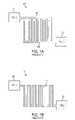
- FIGS. 1A and 1Bare diagrams illustrating conventional probe-able comb and serpentine structures, respectively.
- a conventional probe-able comb test structure 100is provided.
- the conventional probe-able comb test structure 100includes a plurality of probe pads 101 and 102 respectively connected to comb-like structures 103 and 104 .
- a conventional probe-able serpentine test structure 110is provided.
- the conventional probe-able serpentine test structure 110includes a plurality of probe pads 111 and 112 and a single meandering metal or wire 113 connected therebetween.
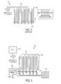
- FIG. 2illustrates a conventional voltage contrast test structure 200 .
- the conventional voltage contrast test structure 200includes a grounded comb 201 including a plurality of grounded tines 202 , and a plurality of floating tines 203 where each floating tine 203 is in between each grounded tine 202 . These floating tines 203 are independent to allow defect isolation. To test for a short, end portions of the floating tines 203 are scanned in a scan area 204 and if there is a bridge from any one of the floating tines 203 to any of the grounded tines 202 , the respective floating tine 203 becomes grounded.
- the masking areahas a limited amount of space.
- the probe-able test structures and the voltage contrast test structuretypically are allocated in separate areas since they are designed differently. Therefore, a large amount of space within the masking area is used to accommodate these test structures.
- Embodiments of the present inventionprovide probe-able voltage contrast comb and serpentine test structures which save space within the masking area. These test structures may be inspected for defects using voltage contrast inspection where the exact defect location may be isolated and/or they may be electrically probed. In addition to the saving space, the data from these techniques can be compared to ensure each technique is performing accurately and to more thoroughly characterize the defectivity.
- a test structurefor detecting defects within integrated circuits.
- the test structureincludes first, second and third probe pads, the first probe pad being connected to ground, a comb-like structure including a plurality of grounded tines connected to the first probe pad, and a plurality of floating tines, each floating tine provided in between the grounded tines.
- the test structurefurther includes a plurality of switching devices, each switching device coupled with an end portion of each floating tine, and connecting the floating tines to the second probe pad, and the third probe pad is a control pad connected to the plurality of switching devices, which controls on and off states of the switching devices during testing.
- a test structurefor detecting defects within integrated circuits.
- the test structureincludes first, second, third and fourth probe pads, the first probe pad being connected to ground, a comb-like structure including a plurality of grounded tines and connected to the first probe pad, and a plurality of floating tines, each floating tine provided in between the grounded tines and each floating tine connected together between the second and third probe pads.
- the test structurefurther includes a plurality of switching devices, each switching device connected to an end portion of each floating tine and connecting the floating tines to the second and third probe pads, and the fourth probe pad is a control pad connected to the plurality of switching devices, which controls on and off states of the switching devices during testing.
- a method of detecting shorts using a test structure having first and second probe pads and a plurality of grounded tines connected with the first probe padincludes pulling a gate of each of the plurality of switching devices down via a resistor, to turn off the plurality of the switching devices, disconnecting the plurality of floating tines from each other and the second probe pad.
- the methodfurther includes scanning the test structure via an electron beam inspection tool to detect floating tines in the plurality of grounded tines, and grounded tines in the plurality of floating tines.
- a method of detectingopens and shorts using a test structure having first, second and third probe pads and a plurality of grounded tines connected with the first probe pad.
- the methodincludes pulling a gate of each of the plurality of switching devices down via a resistor to turn off the switching devices, isolating the plurality of floating tines between the second probe pad and the third probe pad.
- the methodfurther includes scanning the test structure via an electron inspection tool and detecting opens in the grounded tines and shorts in the floating tines.
- FIGS. 1A and 1Bare diagrams illustrating conventional probe-able comb and serpentine test structures, respectively.
- FIG. 2is a diagram illustrating a conventional voltage contrast (VC) comb test structure.
- FIG. 3is a diagram illustrating a probe-able VC comb test structure that can be implemented within embodiments of the present invention.
- FIG. 4is a diagram illustrating an example of the probe-able VC comb test structure shown in FIG. 3 , having a short detected in-line with a voltage contrast inspection that can be implemented within embodiments of the present invention.
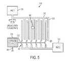
- FIG. 5is a diagram illustrating an example of the probe-able VC comb test structure shown in FIG. 3 , during an electrical test operation that can be implemented within alternative embodiments of the present invention.
- FIG. 6is a diagram illustrating a probe-able VC serpentine test structure that can be implemented within embodiments of the present invention.
- FIGS. 7A and 7Bare flowcharts respectively illustrating a method for detecting shorts using the probe-able VC comb test structure shown in FIG. 3 during in-line testing via an inspection scanning electron microscope (SEM) and end of line testing via a prober, in accordance with an embodiment of the present invention.
- SEMinspection scanning electron microscope
- FIGS. 8A and 8Bare flowcharts respectively illustrating a method for detecting opens and shorts using the VC serpentine test structure shown in FIG. 6 during in-line test via an inspection SEM and end of line testing via a prober, in accordance with an embodiment of the present invention.
- a probe-able VC comb test structure 300includes a plurality of probe pads (i.e., first and second probe pads 305 and 310 ), wherein the first probe pad 305 is connected to ground.
- the test structure 300further includes a comb-like structure (i.e., a grounded comb 315 ) which includes a plurality of grounded tines 320 .
- the test structure 300further includes a plurality of floating tines 325 . Each floating tine 325 is provided in between each grounded tine 320 for detection of shorts (as depicted in FIG. 4 , for example).
- the test structure 300further includes a plurality of active switching devices 330 corresponding to each of the plurality of floating tines 325 .
- Each switching device 330is coupled with an end portion of each floating tine 325 .
- the switching devices 330connect the plurality of floating tines 325 to the probe pad 310 , for selectively connecting the floating tines 325 together.
- the switching devices 330may each include an n-type field effect transistor (nFET). That is, each floating tine 325 is connected to a respective switching device 330 which is in turn connected to probe pad 310 such that all of the floating tines 325 are connected together and to probe pad 310 .
- the width of each of the floating tines 325is substantially similar to one another.
- the probe-able voltage contrast test structure 300further includes a third probe pad (i.e., a control pad 335 ) coupled to the switching devices 330 .
- the control pad 335controls an on/off state of the switching devices 330 .
- the probe-able voltage contrast test structure 300further includes a resistor 340 wherein the control pad 335 is connected through the resistor 340 to ground.
- Each gate 332 of the switching devices 330are connected to the control pad 335 and in turn connected to ground via the resistor 340 .
- the switching devices 330are forced off by the resistor 340 during voltage contrast inspection because the control pad 335 is connected through the resistor 340 to ground. Therefore, each floating tine 325 is isolated.
- a chargeis induced on the floating tines 325 to detect any shorts.
- the switching devices 330are used to transform the floating tines 325 (i.e., electrical nodes) of the VC comb test structure 300 or other test structure into a single electrical node which is connected to the probe pad 310 .
- An example of the detection of a shortwill now be discussed below with reference to FIG. 4 .
- FIG. 4is an example of the probe-able VC comb test structure 300 shown in FIG. 3 , having a short during voltage contrast inspection.
- the control pad 335controls the switching devices 330 to be in an off state. That is, the gates 332 of the switching devices 330 are pulled to ground through the resistor 340 so that the switching devices 330 are off during voltage contrast inspection. Therefore, each floating tine 325 is isolated.
- the gate 332 of each switching device 330may be tied to ground or a virtual ground through a resistor.
- the test structure 300is scanned with a scanning electron microscope (SEM) and the SEM induces a charge on all the electrically floating tines 325 while the grounded tines 320 remain in a grounded state.
- SEMscanning electron microscope
- the respective tine 325 abecomes grounded and turns bright.
- the grounded tines 320emit more electrons than the floating tines 325 under electron extraction conditions thereby causing them to appear brighter than the floating tines 325 .
- the other floating tines 325remain dark.
- FIG. 5is an example of the probe-able VC comb test structure 300 shown in FIG. 3 , during an electrical test operation.
- the switching devices 330are turned on by pulling the control pad 335 ‘high’ and all of the floating tines 325 which are normally isolated are shorted together and connected to the probe pad 310 whereas the grounded tines 320 are connected to the probe pad 305 .
- probe pad 310is checking for shorts and when a short 350 exists, all of the tines 325 become grounded.
- the control pad 335 connected to the gates 332 of all the switching devices 330is biased to a positive voltage greater than a threshold voltage, which may be approximately 0.15 volts (V).
- the control pad 335is on therefore turning the switching devices 330 on during probing. All the normally floating tines 325 are then shorted into “one large bottom comb”. The same short defect now causes the entire bottom comb to be shorted to the grounded comb 315 (as shown in FIG. 5 , for example).
- FIG. 6is a diagram illustrating a probe-able voltage contrast serpentine test structure 600 which tests for opens which may occur due to missing conductive material defects.
- the test structure 600includes a plurality of probe pads (i.e., first, second and third probe pads) 605 , 610 , and 615 .
- the first probe pad 605is connected to ground.
- the test structure 600further includes a grounded comb 617 including a plurality of grounded tines 620 which are connected to the first probe pad 605 .
- the test structure 600further includes a plurality of floating tines 625 . Each floating tine 625 is provided in between each grounded tine 620 and each floating tine 620 may be connected together between the second and third probe pads 610 and 615 .
- the test structure 600further includes a plurality of switching devices 630 .
- Each switching device 630is connected to an end portion of each floating tine 625 and connects the floating tines 625 to the second and third probe pads 610 and 615 .
- some of the switching devices 630i.e., switching devices 630 a , 630 b , 630 c and 630 d
- the remaining switching devices 630i.e., switching devices 630 e , 630 f and 630 g
- the switching devices 630may be nFETs.
- the probe-able voltage contrast serpentine test structure 600further includes a fourth probe pad (i.e., a control pad 635 ) connected to the plurality of switching devices 630 , which controls on and off states of the switching devices 630 .
- a fourth probe padi.e., a control pad 635
- gates 632 of the switching devices 630are all connected to the control pad 635 .
- the switching devices 630are in an off state and connected to ground through a resistor 640 connected to the control pad 635 , and opens are detected in the grounded tines 620 of the grounded comb 617 .
- the switching devices 630are switched to an on state by the control pad 635 and opens are detected in the floating tines 625 from the probe pad 610 to the probe pad 615 by measuring the resistance from the probe pad 610 to the probe pad 615 .
- FIGS. 7A and 7Bare flowcharts respectively illustrating a method for detecting shorts using the test structure shown in FIG. 3 during in-line testing via an inspection SEM and end of line testing via prober.
- in-line testingis performed via an inspection SEM.
- the methodis performed using a test structure having first and second probe pads and a plurality of grounded tines connected with the first probe pad.
- a gate of each of the plurality of switching devicesis pulled down via a resistor to turn off the plurality of switching devices, disconnecting the plurality of floating tines from each other and the second probe pad.
- the processmoves to operation 705 where the test structure is scanned via an electron beam inspection tool to detect floating tines in the plurality of grounded tines and grounded tines in the plurality of floating tines.
- end of line testingis performed via a prober.
- a control padis forced to a positive voltage greater than a threshold voltage to turn on the switching devices during probing, and to connect the isolated floating tines together and to the second probe pad.
- the processmoves to operation 715 , where a resistance is measured between the first and second probe pads to detect any shorts from the floating tines to the grounded tines via a prober.
- the threshold voltageis approximately 0.15 volts (V).
- FIGS. 8B and 8Bare flowcharts respectively illustrating a method for detecting opens and shorts using the test structure shown in FIG. 6 during in-line testing via an inspection SEM and end of line testing via a prober.
- in-line testingis performed via an inspection SEM.
- the methodis performed using a test structure having first, second and third probe pads and a plurality of grounded tines connected with the first probe pad.
- a gate of each of the plurality of switching devicesis pulled down via a resistor to turn off the switching devices, isolating the plurality of floating tines between the second probe pad and the third probe pad.
- the processmoves to operation 805 where the test structure is scanned via an electron beam inspection tool to detect opens in the grounded tines and shorts in the floating tines.
- end of line testingis performed via a prober.
- a control padis forced to a positive voltage greater than a threshold voltage to turn on the switching devices during probing, and to connect the floating tines together and to the second and third probe pads.
- the processmoves to operation 815 , where a resistance between the second and third probe pads is measured to detect opens in the floating tines and a resistance between the first and second probe pads is measured to detect shorts from the floating tines to the grounded tines via a prober.
- the same areais used for testing shorts and opens.
- the present inventionprovides the advantage of saving masking space. Further, the data generated from both these techniques may be compared to ensure that each technique is performing properly.
Landscapes
- Engineering & Computer Science (AREA)
- Computer Hardware Design (AREA)
- Microelectronics & Electronic Packaging (AREA)
- General Engineering & Computer Science (AREA)
- Physics & Mathematics (AREA)
- General Physics & Mathematics (AREA)
- Testing Or Measuring Of Semiconductors Or The Like (AREA)
- Tests Of Electronic Circuits (AREA)
Abstract
Description
This invention relates to test structures for semiconductor fabrication, and more particularly to probe-able voltage contrast test structures for electrical testing and voltage contrast inspection, and a method for detecting defects using the same.
Mask area (space on the reticle) is a precious resource used during technology development and manufacturing of integrated circuits. Mask sets may cost 1 million dollars or more. During process development a wide range of test structures for characterizing the yield and functionality of different circuit components must incorporated on each mask set. In addition, design IP must also be included to test out the building blocks for ICs that will be manufacturing for sale. During manufacturing, primarily chips that will be sold consume the entire mask area. Generally there is not enough room on a mask set to accommodate all the test structures and other designs that could provide value Two classes of test structures often included on mask sets are probe-able test structures (e.g., combs and serpentine patterns) which are used to test for shorts and opens using electrical probes, and voltage contrast test structures which are used in line with a scanning electron microscope (SEM). The voltage contrast test structures provide feedback on defectivity at a level shortly after defect formation. The exact location of each defect is also isolated using this technique. Probe-able test structures are important because they enable a very large area to be tested quickly. Voltage contrast inspection is time consuming and so many wafers go without inspection. A greater number of wafers can be probed. Also using electrical probes, the exact resistance can be measured.
Probe-able test structures and voltage contrast test structures are different in structure. Probe-able test structures require large probe pads, which are connect to two or more electrical nodes in the structure.FIGS. 1A and 1B are diagrams illustrating conventional probe-able comb and serpentine structures, respectively. As shown in FIG.1A, a conventional probe-ablecomb test structure 100 is provided. The conventional probe-ablecomb test structure 100 includes a plurality ofprobe pads like structures FIG. 1B , a conventional probe-ableserpentine test structure 110 is provided. The conventional probe-ableserpentine test structure 110, includes a plurality ofprobe pads wire 113 connected therebetween.
On the other hand, a voltage contrast test structure requires smaller electrical nodes for efficient defect isolation.FIG. 2 illustrates a conventional voltagecontrast test structure 200. The conventional voltagecontrast test structure 200 includes agrounded comb 201 including a plurality ofgrounded tines 202, and a plurality offloating tines 203 where eachfloating tine 203 is in between each groundedtine 202. Thesefloating tines 203 are independent to allow defect isolation. To test for a short, end portions of thefloating tines 203 are scanned in ascan area 204 and if there is a bridge from any one of thefloating tines 203 to any of thegrounded tines 202, the respectivefloating tine 203 becomes grounded.
The masking area has a limited amount of space. The probe-able test structures and the voltage contrast test structure typically are allocated in separate areas since they are designed differently. Therefore, a large amount of space within the masking area is used to accommodate these test structures.
Embodiments of the present invention provide probe-able voltage contrast comb and serpentine test structures which save space within the masking area. These test structures may be inspected for defects using voltage contrast inspection where the exact defect location may be isolated and/or they may be electrically probed. In addition to the saving space, the data from these techniques can be compared to ensure each technique is performing accurately and to more thoroughly characterize the defectivity.
According to an embodiment of the present invention, a test structure for detecting defects within integrated circuits is provided. The test structure includes first, second and third probe pads, the first probe pad being connected to ground, a comb-like structure including a plurality of grounded tines connected to the first probe pad, and a plurality of floating tines, each floating tine provided in between the grounded tines. The test structure further includes a plurality of switching devices, each switching device coupled with an end portion of each floating tine, and connecting the floating tines to the second probe pad, and the third probe pad is a control pad connected to the plurality of switching devices, which controls on and off states of the switching devices during testing.
According to another embodiment of the present invention, a test structure for detecting defects within integrated circuits is provided. The test structure includes first, second, third and fourth probe pads, the first probe pad being connected to ground, a comb-like structure including a plurality of grounded tines and connected to the first probe pad, and a plurality of floating tines, each floating tine provided in between the grounded tines and each floating tine connected together between the second and third probe pads. The test structure further includes a plurality of switching devices, each switching device connected to an end portion of each floating tine and connecting the floating tines to the second and third probe pads, and the fourth probe pad is a control pad connected to the plurality of switching devices, which controls on and off states of the switching devices during testing.
According to another embodiment of the present invention, a method of detecting shorts using a test structure having first and second probe pads and a plurality of grounded tines connected with the first probe pad. The method includes pulling a gate of each of the plurality of switching devices down via a resistor, to turn off the plurality of the switching devices, disconnecting the plurality of floating tines from each other and the second probe pad. The method further includes scanning the test structure via an electron beam inspection tool to detect floating tines in the plurality of grounded tines, and grounded tines in the plurality of floating tines.
According to yet another embodiment of the present invention, a method of detecting opens and shorts using a test structure having first, second and third probe pads and a plurality of grounded tines connected with the first probe pad is provided. The method includes pulling a gate of each of the plurality of switching devices down via a resistor to turn off the switching devices, isolating the plurality of floating tines between the second probe pad and the third probe pad. The method further includes scanning the test structure via an electron inspection tool and detecting opens in the grounded tines and shorts in the floating tines.
Additional features and advantages are realized through the techniques of the present invention. Other embodiments and aspects of the invention are described in detail herein and are considered a part of the claimed invention. For a better understanding of the invention with advantages and features, refer to the description and to the drawings.
The subject matter which is regarded as the invention is particularly pointed out and distinctly claimed in the claims at the conclusion of the specification. The foregoing and other objects, features, and advantages of the invention are apparent from the following detailed description taken in conjunction with the accompanying drawings in which:
The detailed description explains the preferred embodiments of the invention, together with advantages and features, by way of example with reference to the drawings.
Turning now to the drawings in greater detail, it will be seen that inFIG. 3 , there is a probe-able VC comb test structure according to an embodiment of the present invention. As shown inFIG. 3 , a probe-able VCcomb test structure 300 includes a plurality of probe pads (i.e., first andsecond probe pads 305 and310), wherein thefirst probe pad 305 is connected to ground. Thetest structure 300 further includes a comb-like structure (i.e., a grounded comb315) which includes a plurality of groundedtines 320. Thetest structure 300 further includes a plurality of floatingtines 325. Each floatingtine 325 is provided in between each groundedtine 320 for detection of shorts (as depicted inFIG. 4 , for example).
According to an embodiment of the present invention, thetest structure 300 further includes a plurality ofactive switching devices 330 corresponding to each of the plurality of floatingtines 325. Eachswitching device 330 is coupled with an end portion of each floatingtine 325. The switchingdevices 330 connect the plurality of floatingtines 325 to theprobe pad 310, for selectively connecting the floatingtines 325 together. According to an embodiment of the present invention, the switchingdevices 330 may each include an n-type field effect transistor (nFET). That is, each floatingtine 325 is connected to arespective switching device 330 which is in turn connected to probepad 310 such that all of the floatingtines 325 are connected together and to probepad 310. According to an embodiment of the present invention, the width of each of the floatingtines 325 is substantially similar to one another.
According to an embodiment of the present invention, the probe-able voltagecontrast test structure 300 further includes a third probe pad (i.e., a control pad335) coupled to theswitching devices 330. Thecontrol pad 335 controls an on/off state of theswitching devices 330. The probe-able voltagecontrast test structure 300 further includes aresistor 340 wherein thecontrol pad 335 is connected through theresistor 340 to ground. Eachgate 332 of theswitching devices 330 are connected to thecontrol pad 335 and in turn connected to ground via theresistor 340. According to the current embodiment, the switchingdevices 330 are forced off by theresistor 340 during voltage contrast inspection because thecontrol pad 335 is connected through theresistor 340 to ground. Therefore, each floatingtine 325 is isolated. A charge is induced on the floatingtines 325 to detect any shorts. The switchingdevices 330 are used to transform the floating tines325 (i.e., electrical nodes) of the VCcomb test structure 300 or other test structure into a single electrical node which is connected to theprobe pad 310. An example of the detection of a short will now be discussed below with reference toFIG. 4 .
During the in-line VC inspection, thetest structure 300 is scanned with a scanning electron microscope (SEM) and the SEM induces a charge on all the electrically floatingtines 325 while the groundedtines 320 remain in a grounded state. Further, as shown, when a short350 exists between a respective floating tine e.g., a floatingtine 325a, for example, and a groundedtine 320 adjacent to therespective tine 325a, therespective tine 325abecomes grounded and turns bright. The groundedtines 320 emit more electrons than the floatingtines 325 under electron extraction conditions thereby causing them to appear brighter than the floatingtines 325. The other floatingtines 325 remain dark.
According to an embodiment of the present invention, thetest structure 600 further includes a plurality of switching devices630. Each switching device630 is connected to an end portion of each floating tine625 and connects the floating tines625 to the second andthird probe pads devices devices
The probe-able voltage contrastserpentine test structure 600 further includes a fourth probe pad (i.e., a control pad635) connected to the plurality of switching devices630, which controls on and off states of the switching devices630. According to an embodiment of the present invention,gates 632 of the switching devices630 are all connected to thecontrol pad 635. During voltage contrast inspection, the switching devices630 are in an off state and connected to ground through aresistor 640 connected to thecontrol pad 635, and opens are detected in the groundedtines 620 of the groundedcomb 617. During probing, the switching devices630 are switched to an on state by thecontrol pad 635 and opens are detected in the floating tines625 from theprobe pad 610 to theprobe pad 615 by measuring the resistance from theprobe pad 610 to theprobe pad 615.
InFIG. 7A , in-line testing is performed via an inspection SEM. In this figure, the method is performed using a test structure having first and second probe pads and a plurality of grounded tines connected with the first probe pad. Atoperation 700, a gate of each of the plurality of switching devices is pulled down via a resistor to turn off the plurality of switching devices, disconnecting the plurality of floating tines from each other and the second probe pad. Fromoperation 700, the process moves tooperation 705 where the test structure is scanned via an electron beam inspection tool to detect floating tines in the plurality of grounded tines and grounded tines in the plurality of floating tines.
InFIG. 7B , end of line testing is performed via a prober. According to an embodiment of the present invention, atoperation 710, a control pad is forced to a positive voltage greater than a threshold voltage to turn on the switching devices during probing, and to connect the isolated floating tines together and to the second probe pad. Fromoperation 710, the process moves tooperation 715, where a resistance is measured between the first and second probe pads to detect any shorts from the floating tines to the grounded tines via a prober.
According to an embodiment of the present invention, the threshold voltage is approximately 0.15 volts (V).
InFIG. 8A , in-line testing is performed via an inspection SEM. In this figure, the method is performed using a test structure having first, second and third probe pads and a plurality of grounded tines connected with the first probe pad. Atoperation 800, a gate of each of the plurality of switching devices is pulled down via a resistor to turn off the switching devices, isolating the plurality of floating tines between the second probe pad and the third probe pad. Fromoperation 800, the process moves tooperation 805 where the test structure is scanned via an electron beam inspection tool to detect opens in the grounded tines and shorts in the floating tines.
InFIG. 8B , end of line testing is performed via a prober. According to an embodiment of the present invention, atoperation 810, a control pad is forced to a positive voltage greater than a threshold voltage to turn on the switching devices during probing, and to connect the floating tines together and to the second and third probe pads. Fromoperation 810, the process moves tooperation 815, where a resistance between the second and third probe pads is measured to detect opens in the floating tines and a resistance between the first and second probe pads is measured to detect shorts from the floating tines to the grounded tines via a prober.
According to an embodiment of the present invention, the same area is used for testing shorts and opens. Thus, the present invention provides the advantage of saving masking space. Further, the data generated from both these techniques may be compared to ensure that each technique is performing properly.
While the preferred embodiment to the invention has been described, it will be understood that those skilled in the art, both now and in the future, may make various improvements and enhancements which fall within the scope of the claims which follow. These claims should be construed to maintain the proper protection for the invention first described.
Claims (5)
1. A test structure comprising:
first, second and third probe pads, the first probe pad being connected to ground;
a comb-like structure including a plurality of grounded tines connected to the first probe pad;
a plurality of floating tines, each floating tine provided in between the grounded tines;
a plurality of switching devices, each switching device coupled with an end portion of each floating tine, and connecting the floating tines to the second probe pad; and
the third probe pad being a control pad connected to the plurality of switching devices, which controls on and off states of the switching devices during testing, wherein the control pad is connected through a resistor to ground, with gates of the switching devices being connected to the control pad and grounded via the resistor; and
during voltage contrast inspection, the switching devices are forced off by the resistor and a charge is induced on the floating tines to detect any shorts, and when a short exists between a respective floating tine and a grounded tine adjacent to the respective floating tine, the respective floating tine is grounded.
2. The test structure ofclaim 1 , wherein the switching devices are n-type field effect transistors.
3. The test structure ofclaim 1 , wherein the voltage contrast inspection is performed using a scanning electron microscope.
4. A test structure comprising:
first, second and third probe pads, the first probe pad being connected to ground;
a comb-like structure including a plurality of grounded tines connected to the first probe pad;
a plurality of floating tines, each floating tine provided in between the grounded tines;
a plurality of switching devices, each switching device coupled with an end portion of each floating tine, and connecting the floating tines to the second probe pad; and
the third probe pad being a control pad connected to the plurality of switching devices, which controls on and off states of the switching devices during testing, wherein the control pad is connected through a resistor to ground, with gates of the switching devices being connected to the control pad and grounded via the resistor; and
during probing, the switching devices are turned on, wherein when a short exists between a respective floating tine and a grounded tine adjacent to the respective floating tine, the plurality of the floating tines and the second probe pad are grounded.
5. The test structure ofclaim 4 , wherein during probing, the control pad is biased to a positive voltage greater than approximately 0.15 volts (V) to turn on the switching devices.
Priority Applications (4)
| Application Number | Priority Date | Filing Date | Title |
|---|---|---|---|
| US12/539,732US8350583B2 (en) | 2009-08-12 | 2009-08-12 | Probe-able voltage contrast test structures |
| US13/593,983US9097760B2 (en) | 2009-08-12 | 2012-08-24 | Probe-able voltage contrast test structures |
| US13/593,961US9213060B2 (en) | 2009-08-12 | 2012-08-24 | Probe-able voltage contrast test structures |
| US13/593,975US9103875B2 (en) | 2009-08-12 | 2012-08-24 | Probe-able voltage contrast test structures |
Applications Claiming Priority (1)
| Application Number | Priority Date | Filing Date | Title |
|---|---|---|---|
| US12/539,732US8350583B2 (en) | 2009-08-12 | 2009-08-12 | Probe-able voltage contrast test structures |
Related Child Applications (3)
| Application Number | Title | Priority Date | Filing Date |
|---|---|---|---|
| US13/593,975DivisionUS9103875B2 (en) | 2009-08-12 | 2012-08-24 | Probe-able voltage contrast test structures |
| US13/593,983DivisionUS9097760B2 (en) | 2009-08-12 | 2012-08-24 | Probe-able voltage contrast test structures |
| US13/593,961DivisionUS9213060B2 (en) | 2009-08-12 | 2012-08-24 | Probe-able voltage contrast test structures |
Publications (2)
| Publication Number | Publication Date |
|---|---|
| US20110037493A1 US20110037493A1 (en) | 2011-02-17 |
| US8350583B2true US8350583B2 (en) | 2013-01-08 |
Family
ID=43588220
Family Applications (4)
| Application Number | Title | Priority Date | Filing Date |
|---|---|---|---|
| US12/539,732Expired - Fee RelatedUS8350583B2 (en) | 2009-08-12 | 2009-08-12 | Probe-able voltage contrast test structures |
| US13/593,961Expired - Fee RelatedUS9213060B2 (en) | 2009-08-12 | 2012-08-24 | Probe-able voltage contrast test structures |
| US13/593,983Expired - Fee RelatedUS9097760B2 (en) | 2009-08-12 | 2012-08-24 | Probe-able voltage contrast test structures |
| US13/593,975Expired - Fee RelatedUS9103875B2 (en) | 2009-08-12 | 2012-08-24 | Probe-able voltage contrast test structures |
Family Applications After (3)
| Application Number | Title | Priority Date | Filing Date |
|---|---|---|---|
| US13/593,961Expired - Fee RelatedUS9213060B2 (en) | 2009-08-12 | 2012-08-24 | Probe-able voltage contrast test structures |
| US13/593,983Expired - Fee RelatedUS9097760B2 (en) | 2009-08-12 | 2012-08-24 | Probe-able voltage contrast test structures |
| US13/593,975Expired - Fee RelatedUS9103875B2 (en) | 2009-08-12 | 2012-08-24 | Probe-able voltage contrast test structures |
Country Status (1)
| Country | Link |
|---|---|
| US (4) | US8350583B2 (en) |
Cited By (16)
| Publication number | Priority date | Publication date | Assignee | Title |
|---|---|---|---|---|
| US9627371B1 (en) | 2016-04-04 | 2017-04-18 | Pdf Solutions, Inc. | Integrated circuit containing standard logic cells and library-compatible, NCEM-enabled fill cells, including at least via-open-configured, GATE-short-configured, GATECNT-short-configured, and AA-short-configured, NCEM-enabled fill cells |
| US9691672B1 (en) | 2015-12-16 | 2017-06-27 | Pdf Solutions, Inc. | Integrated circuit containing standard logic cells and library-compatible, NCEM-enabled fill cells, including at least via-open-configured, GATE-short-configured, GATECNT-short-configured, and metal-short-configured, NCEM-enabled fill cells |
| US9721938B1 (en) | 2016-04-04 | 2017-08-01 | Pdf Solutions, Inc. | Integrated circuit containing first and second DOEs of standard cell compatible, NCEM-enabled fill cells, with the first DOE including tip-to-tip short configured fill cells, and the second DOE including corner short configured fill cells |
| US9748153B1 (en) | 2017-03-29 | 2017-08-29 | Pdf Solutions, Inc. | Process for making and using a semiconductor wafer containing first and second does of standard cell compatible, NCEM-enabled fill cells, with the first DOE including side-to-side short configured fill cells, and the second DOE including tip-to-side short configure |
| US9768083B1 (en) | 2017-06-27 | 2017-09-19 | Pdf Solutions, Inc. | Process for making and using a semiconductor wafer containing first and second DOEs of standard cell compatible, NCEM-enabled fill cells, with the first DOE including merged-via open configured fill cells, and the second DOE including snake open configured fill cells |
| US9773774B1 (en) | 2017-03-30 | 2017-09-26 | Pdf Solutions, Inc. | Process for making and using a semiconductor wafer containing first and second DOEs of standard cell compatible, NCEM-enabled fill cells, with the first DOE including chamfer short configured fill cells, and the second DOE including corner short configured fill cells |
| US9786649B1 (en) | 2017-06-27 | 2017-10-10 | Pdf Solutions, Inc. | Process for making and using a semiconductor wafer containing first and second DOEs of standard cell compatible, NCEM-enabled fill cells, with the first DOE including via open configured fill cells, and the second DOE including stitch open configured fill cells |
| US9805994B1 (en) | 2015-02-03 | 2017-10-31 | Pdf Solutions, Inc. | Mesh-style NCEM pads, and process for making semiconductor dies, chips, and wafers using in-line measurements from such pads |
| US9865583B1 (en) | 2017-06-28 | 2018-01-09 | Pdf Solutions, Inc. | Process for making and using a semiconductor wafer containing first and second DOEs of standard cell compatible, NCEM-enabled fill cells, with the first DOE including snake open configured fill cells, and the second DOE including stitch open configured fill cells |
| US9929063B1 (en) | 2016-04-04 | 2018-03-27 | Pdf Solutions, Inc. | Process for making an integrated circuit that includes NCEM-Enabled, tip-to-side gap-configured fill cells, with NCEM pads formed from at least three conductive stripes positioned between adjacent gates |
| US10096530B1 (en) | 2017-06-28 | 2018-10-09 | Pdf Solutions, Inc. | Process for making and using a semiconductor wafer containing first and second DOEs of standard cell compatible, NCEM-enabled fill cells, with the first DOE including merged-via open configured fill cells, and the second DOE including stitch open configured fill cells |
| US10199289B1 (en) | 2015-02-03 | 2019-02-05 | Pdf Solutions, Inc. | Method for processing a semiconductor wafer using non-contact electrical measurements indicative of at least one chamfer short or leakage, at least one corner short or leakage, and at least one via open or resistance, where such measurements are obtained from non-contact pads associated with respective chamfer short, corner short, and via open test areas |
| US10593604B1 (en) | 2015-12-16 | 2020-03-17 | Pdf Solutions, Inc. | Process for making semiconductor dies, chips, and wafers using in-line measurements obtained from DOEs of NCEM-enabled fill cells |
| US10978438B1 (en) | 2015-12-16 | 2021-04-13 | Pdf Solutions, Inc. | IC with test structures and E-beam pads embedded within a contiguous standard cell area |
| US11315841B2 (en) | 2019-04-18 | 2022-04-26 | Samsung Electronics Co., Ltd. | Pattern design for integrated circuits and method for inspecting the pattern design for integrated circuits |
| US12444661B2 (en) | 2019-04-18 | 2025-10-14 | Samsung Electronics Co., Ltd. | Pattern design for integrated circuits and method for inspecting the pattern design for integrated circuits |
Families Citing this family (4)
| Publication number | Priority date | Publication date | Assignee | Title |
|---|---|---|---|---|
| US10276346B1 (en) | 2016-03-09 | 2019-04-30 | Kla-Tencor Corporation | Particle beam inspector with independently-controllable beams |
| CN107579016B (en)* | 2017-08-31 | 2018-09-14 | 长江存储科技有限责任公司 | A kind of interdigitated test structure |
| CN109490758B (en)* | 2018-12-12 | 2020-12-15 | 上海华力集成电路制造有限公司 | Short circuit failure positioning method |
| TWI696207B (en)* | 2019-03-04 | 2020-06-11 | 力晶積成電子製造股份有限公司 | Test structure for charged particle beam inspection and method for defect determination using the same |
Citations (33)
| Publication number | Priority date | Publication date | Assignee | Title |
|---|---|---|---|---|
| US4565966A (en) | 1983-03-07 | 1986-01-21 | Kollmorgen Technologies Corporation | Method and apparatus for testing of electrical interconnection networks |
| US5189306A (en) | 1992-03-24 | 1993-02-23 | International Business Machines Corporation | Grey-splice algorithm for electron beam lithography post-processor |
| US5266901A (en) | 1992-05-29 | 1993-11-30 | International Business Machines Corp. | Apparatus and method for resistive detection and waveform analysis of interconenction networks |
| US5539306A (en) | 1995-01-24 | 1996-07-23 | International Business Machines Corporation | Method and apparatus for testing electrical and electronic circuits |
| US6297644B1 (en) | 1999-03-04 | 2001-10-02 | Advanced Micro Devices, Inc. | Multipurpose defect test structure with switchable voltage contrast capability and method of use |
| US20020117696A1 (en)* | 2001-02-27 | 2002-08-29 | Toshikazu Hirai | Semiconductor switching device |
| US6452412B1 (en) | 1999-03-04 | 2002-09-17 | Advanced Micro Devices, Inc. | Drop-in test structure and methodology for characterizing an integrated circuit process flow and topography |
| US6509197B1 (en) | 1999-12-14 | 2003-01-21 | Kla-Tencor Corporation | Inspectable buried test structures and methods for inspecting the same |
| US6544802B1 (en) | 1999-10-16 | 2003-04-08 | Samsung Electronics Co., Ltd. | Wafer inspection system and method for selectively inspecting conductive pattern defects |
| US20030096436A1 (en) | 1999-12-14 | 2003-05-22 | Kla-Tencor Technologies Corporation | Test structures and methods for inspection of semiconductor integrated circuits |
| JP2004184257A (en) | 2002-12-04 | 2004-07-02 | Kura Gijutsu Kenkyusho:Kk | A circuit for detecting a small difference between two pairs of resistors or coils or capacitors, a position detecting device using the circuit, and an inspection device for detecting defects or presence or absence of conductors |
| US6815959B2 (en) | 2001-04-09 | 2004-11-09 | Kla-Tencor Technologies Corp. | Systems and methods for measuring properties of conductive layers |
| US6861666B1 (en) | 2001-10-17 | 2005-03-01 | Kla-Tencor Technologies Corporation | Apparatus and methods for determining and localization of failures in test structures using voltage contrast |
| JP2005210146A (en) | 2003-01-09 | 2005-08-04 | Kura Gijutsu Kenkyusho:Kk | Two circuit element minute difference detection circuit, position detection device using the same, magnetic substance or conductor defect inspection device |
| US7026175B2 (en) | 2004-03-29 | 2006-04-11 | Applied Materials, Inc. | High throughput measurement of via defects in interconnects |
| US7081758B2 (en) | 2001-08-14 | 2006-07-25 | Oki Electric Industry Co., Ltd. | Inspection pattern, inspection method, and inspection system for detection of latent defect of multi-layer wiring structure |
| US20060192904A1 (en) | 2002-10-03 | 2006-08-31 | Gilad Almogy | System and method for defect localization on electrical test structures |
| US20080032429A1 (en) | 2005-11-09 | 2008-02-07 | Da Chen | Methods, defect review tools, and systems for locating a defect in a defect review process |
| US7340703B2 (en) | 2004-08-02 | 2008-03-04 | Hazem Mahmoud Hegazy | Test structures and method for interconnect impedance property extraction |
| US20080100831A1 (en) | 2006-10-31 | 2008-05-01 | International Business Machines Corporation | Method, apparatus, and computer program product for optimizing inspection recipes using programmed defects |
| US20080217612A1 (en) | 2007-03-07 | 2008-09-11 | International Business Machines Corporation | Structure and method of mapping signal intensity to surface voltage for integrated circuit inspection |
| US20080237586A1 (en) | 2007-03-30 | 2008-10-02 | Min Chul Sun | Semiconductor Integrated Test Structures For Electron Beam Inspection of Semiconductor Wafers |
| US7456636B2 (en) | 2006-03-29 | 2008-11-25 | International Business Machines Corporation | Test structures and method of defect detection using voltage contrast inspection |
| US7474107B2 (en) | 2006-03-22 | 2009-01-06 | International Business Machines Corporation | Buried short location determination using voltage contrast inspection |
| US20090057644A1 (en) | 2007-08-24 | 2009-03-05 | Samsung Electronics Co., Ltd | Phase-change memory units, methods of forming the phase-change memory units, phase-change memory devices having the phase-change memory units and methods of manufacturung the phase-change memory devices |
| US7518190B2 (en) | 2006-03-22 | 2009-04-14 | International Business Machines Corporation | Grounding front-end-of-line structures on a SOI substrate |
| US20090096461A1 (en) | 2007-10-15 | 2009-04-16 | International Business Machines Corporation | Test structure and method for resistive open detection using voltage contrast inspection |
| US7592827B1 (en)* | 2007-01-12 | 2009-09-22 | Pdf Solutions, Inc. | Apparatus and method for electrical detection and localization of shorts in metal interconnect lines |
| US7683644B2 (en) | 2007-08-06 | 2010-03-23 | International Business Machines Corporation | Extrusion failure monitor structures |
| US7795879B2 (en) | 2005-10-28 | 2010-09-14 | Advantest Corporation | Testing apparatus |
| US20100279436A1 (en) | 2009-04-30 | 2010-11-04 | Taiwan Semiconductor Manufacturing Company, Ltd. | Inspection Method For Integrated Circuit Manufacturing Processes |
| US7927895B1 (en) | 2009-10-06 | 2011-04-19 | International Business Machines Corporation | Varying capacitance voltage contrast structures to determine defect resistance |
| US8039837B2 (en) | 2009-05-26 | 2011-10-18 | International Business Machines Corporation | In-line voltage contrast detection of PFET silicide encroachment |
Family Cites Families (2)
| Publication number | Priority date | Publication date | Assignee | Title |
|---|---|---|---|---|
| JP4272968B2 (en)* | 2003-10-16 | 2009-06-03 | エルピーダメモリ株式会社 | Semiconductor device and semiconductor chip control method |
| US8399266B2 (en) | 2011-01-25 | 2013-03-19 | International Business Machines Corporation | Test structure for detection of gap in conductive layer of multilayer gate stack |
- 2009
- 2009-08-12USUS12/539,732patent/US8350583B2/ennot_activeExpired - Fee Related
- 2012
- 2012-08-24USUS13/593,961patent/US9213060B2/ennot_activeExpired - Fee Related
- 2012-08-24USUS13/593,983patent/US9097760B2/ennot_activeExpired - Fee Related
- 2012-08-24USUS13/593,975patent/US9103875B2/ennot_activeExpired - Fee Related
Patent Citations (35)
| Publication number | Priority date | Publication date | Assignee | Title |
|---|---|---|---|---|
| US4565966A (en) | 1983-03-07 | 1986-01-21 | Kollmorgen Technologies Corporation | Method and apparatus for testing of electrical interconnection networks |
| US5189306A (en) | 1992-03-24 | 1993-02-23 | International Business Machines Corporation | Grey-splice algorithm for electron beam lithography post-processor |
| US5266901A (en) | 1992-05-29 | 1993-11-30 | International Business Machines Corp. | Apparatus and method for resistive detection and waveform analysis of interconenction networks |
| US5539306A (en) | 1995-01-24 | 1996-07-23 | International Business Machines Corporation | Method and apparatus for testing electrical and electronic circuits |
| US6297644B1 (en) | 1999-03-04 | 2001-10-02 | Advanced Micro Devices, Inc. | Multipurpose defect test structure with switchable voltage contrast capability and method of use |
| US6452412B1 (en) | 1999-03-04 | 2002-09-17 | Advanced Micro Devices, Inc. | Drop-in test structure and methodology for characterizing an integrated circuit process flow and topography |
| US6544802B1 (en) | 1999-10-16 | 2003-04-08 | Samsung Electronics Co., Ltd. | Wafer inspection system and method for selectively inspecting conductive pattern defects |
| US6921672B2 (en) | 1999-12-14 | 2005-07-26 | Kla-Tencor Technologies Corporation | Test structures and methods for inspection of semiconductor integrated circuits |
| US6509197B1 (en) | 1999-12-14 | 2003-01-21 | Kla-Tencor Corporation | Inspectable buried test structures and methods for inspecting the same |
| US20030096436A1 (en) | 1999-12-14 | 2003-05-22 | Kla-Tencor Technologies Corporation | Test structures and methods for inspection of semiconductor integrated circuits |
| US20020117696A1 (en)* | 2001-02-27 | 2002-08-29 | Toshikazu Hirai | Semiconductor switching device |
| US6815959B2 (en) | 2001-04-09 | 2004-11-09 | Kla-Tencor Technologies Corp. | Systems and methods for measuring properties of conductive layers |
| US7081758B2 (en) | 2001-08-14 | 2006-07-25 | Oki Electric Industry Co., Ltd. | Inspection pattern, inspection method, and inspection system for detection of latent defect of multi-layer wiring structure |
| US6861666B1 (en) | 2001-10-17 | 2005-03-01 | Kla-Tencor Technologies Corporation | Apparatus and methods for determining and localization of failures in test structures using voltage contrast |
| US20060192904A1 (en) | 2002-10-03 | 2006-08-31 | Gilad Almogy | System and method for defect localization on electrical test structures |
| JP2004184257A (en) | 2002-12-04 | 2004-07-02 | Kura Gijutsu Kenkyusho:Kk | A circuit for detecting a small difference between two pairs of resistors or coils or capacitors, a position detecting device using the circuit, and an inspection device for detecting defects or presence or absence of conductors |
| JP2005210146A (en) | 2003-01-09 | 2005-08-04 | Kura Gijutsu Kenkyusho:Kk | Two circuit element minute difference detection circuit, position detection device using the same, magnetic substance or conductor defect inspection device |
| US7026175B2 (en) | 2004-03-29 | 2006-04-11 | Applied Materials, Inc. | High throughput measurement of via defects in interconnects |
| US7340703B2 (en) | 2004-08-02 | 2008-03-04 | Hazem Mahmoud Hegazy | Test structures and method for interconnect impedance property extraction |
| US7795879B2 (en) | 2005-10-28 | 2010-09-14 | Advantest Corporation | Testing apparatus |
| US20080032429A1 (en) | 2005-11-09 | 2008-02-07 | Da Chen | Methods, defect review tools, and systems for locating a defect in a defect review process |
| US7518190B2 (en) | 2006-03-22 | 2009-04-14 | International Business Machines Corporation | Grounding front-end-of-line structures on a SOI substrate |
| US7474107B2 (en) | 2006-03-22 | 2009-01-06 | International Business Machines Corporation | Buried short location determination using voltage contrast inspection |
| US7456636B2 (en) | 2006-03-29 | 2008-11-25 | International Business Machines Corporation | Test structures and method of defect detection using voltage contrast inspection |
| US20080100831A1 (en) | 2006-10-31 | 2008-05-01 | International Business Machines Corporation | Method, apparatus, and computer program product for optimizing inspection recipes using programmed defects |
| US7592827B1 (en)* | 2007-01-12 | 2009-09-22 | Pdf Solutions, Inc. | Apparatus and method for electrical detection and localization of shorts in metal interconnect lines |
| US20080217612A1 (en) | 2007-03-07 | 2008-09-11 | International Business Machines Corporation | Structure and method of mapping signal intensity to surface voltage for integrated circuit inspection |
| US20080237586A1 (en) | 2007-03-30 | 2008-10-02 | Min Chul Sun | Semiconductor Integrated Test Structures For Electron Beam Inspection of Semiconductor Wafers |
| US7683644B2 (en) | 2007-08-06 | 2010-03-23 | International Business Machines Corporation | Extrusion failure monitor structures |
| US20090057644A1 (en) | 2007-08-24 | 2009-03-05 | Samsung Electronics Co., Ltd | Phase-change memory units, methods of forming the phase-change memory units, phase-change memory devices having the phase-change memory units and methods of manufacturung the phase-change memory devices |
| US20090096461A1 (en) | 2007-10-15 | 2009-04-16 | International Business Machines Corporation | Test structure and method for resistive open detection using voltage contrast inspection |
| US7733109B2 (en) | 2007-10-15 | 2010-06-08 | International Business Machines Corporation | Test structure for resistive open detection using voltage contrast inspection and related methods |
| US20100279436A1 (en) | 2009-04-30 | 2010-11-04 | Taiwan Semiconductor Manufacturing Company, Ltd. | Inspection Method For Integrated Circuit Manufacturing Processes |
| US8039837B2 (en) | 2009-05-26 | 2011-10-18 | International Business Machines Corporation | In-line voltage contrast detection of PFET silicide encroachment |
| US7927895B1 (en) | 2009-10-06 | 2011-04-19 | International Business Machines Corporation | Varying capacitance voltage contrast structures to determine defect resistance |
Non-Patent Citations (10)
| Title |
|---|
| EE Times, [online]; [retrieved on Oct. 18, 2011]; retrieved from the Internet http://eetimes.com/design/communications-design/401791 4/Accurate-Modeling-of-Spiral-Inductors-on-Silicon-for-Wireless-RFIC-Designs Jan Van Hese, "Accurate Modeling of Spiral Inductors on Silicon for Wireless RFIC Designs," EE Times-Design; pp. 1-9; 2001. |
| J.C. Lee, C.H. Chen, D. Su, J.H. Chuang, "Investigation of Sensitivity Improvement on Passive Voltage Contrast for Defect Isolation", Microelectronics Reliability, vol. 42, No. 9-11, pp. 1707-1710, 2002. |
| M. Javed et al., "RLC Circuit Response and Analysis (Using State Space Method)," IJCSNS International Journal of Computer Science and Network Security; vol. 8, No. 4, pp. 48-54, Apr. 2008. |
| M. Matsui, T. Odaka, H. Nagaishi, K. Sakurai, "Quantitative Measurement of Voltage contrast in SEM Images for In-Line Resistance Inspection of Wafers Manufactured for SRAM", Proceedings of the SPIE-The International Society for Optical Engineering, vol. 7272, pp. 72721D (8 pages), 2009. |
| M. Matsui, T. Odaka, H. Nagaishi, K. Sakurai, "Quantitative Measurement of Voltage contrast in SEM Images for In-Line Resistance Inspection of Wafers Manufactured for SRAM", Proceedings of the SPIE—The International Society for Optical Engineering, vol. 7272, pp. 72721D (8 pages), 2009. |
| M. Matsui, Z. Cheng, M. Nozoe, K. Torli, "Detecting Defects in Cu Metallization Structures by Electron-Beam Wafer Inspection", Journal of the Eletrochemical Society, vol. 151, No. 6, pp. G440-2, 2004. |
| O.D. Patterson, H. Wildman, D. Gal, K. Wu, "Detection of Resistive Shorts and Opens Using Voltage Contrast Inspection", Micro, vol. 24, No. 5, pp. 67-68, 2006. |
| Renee T. Mo; pending U.S. Appl. No. 13/013,133 entitled, "Test Structure for Detection of Gap in Conductive Layer of Multilayer Gate Stack,"; filed Jan. 25, 2011. |
| T. Sakai, N. Oda, T. Yokoyama, H. Kikuchi, H. Kitajima, "Defect Isolation and Characterization in Contact Array/Chain Structures by Using Voltage Contrast Effect", Conference Proceedings of IEEE International Symposium on Semiconductor Manufacturing Conference, Santa Clara, CA, Oct. 11-13, 1999., pp. 195-198. |
| Zhao et al.,"Fault-Coverage Analysis Techniques of Crosstalk in Chip Interconnects," IEEE Transactions on Computer-Aided Design of Integrated Circuits and Systems; vol. 22, No. 6, p. 770-782, Jun. 2003. |
Cited By (84)
| Publication number | Priority date | Publication date | Assignee | Title |
|---|---|---|---|---|
| US10199289B1 (en) | 2015-02-03 | 2019-02-05 | Pdf Solutions, Inc. | Method for processing a semiconductor wafer using non-contact electrical measurements indicative of at least one chamfer short or leakage, at least one corner short or leakage, and at least one via open or resistance, where such measurements are obtained from non-contact pads associated with respective chamfer short, corner short, and via open test areas |
| US10199285B1 (en) | 2015-02-03 | 2019-02-05 | Pdf Solutions, Inc. | Method for processing a semiconductor wafer using non-contact electrical measurements indicative of at least one tip-to-tip short or leakage, at least one side-to-side short or leakages, and at least one via respective tip-to-tip short, side-to-side short, and via open test areas |
| US9911649B1 (en) | 2015-02-03 | 2018-03-06 | Pdf Solutions, Inc. | Process for making and using mesh-style NCEM pads |
| US9805994B1 (en) | 2015-02-03 | 2017-10-31 | Pdf Solutions, Inc. | Mesh-style NCEM pads, and process for making semiconductor dies, chips, and wafers using in-line measurements from such pads |
| US10199286B1 (en) | 2015-02-03 | 2019-02-05 | Pdf Solutions, Inc. | Method for processing a semiconductor wafer using non-contact electrical measurements indicative of at least one tip-to-side short or leakage, at least one chamfer short or leakage, and at least one corner short or leakage, where such measurements are obtained from non-contact pads associated with respective tip-to-side short, chamfer short, and corner short test areas |
| US10199283B1 (en) | 2015-02-03 | 2019-02-05 | Pdf Solutions, Inc. | Method for processing a semiconductor wager using non-contact electrical measurements indicative of a resistance through a stitch, where such measurements are obtained by scanning a pad comprised of at least three parallel conductive stripes using a moving stage with beam deflection to account for motion of the stage |
| US10199293B1 (en) | 2015-02-03 | 2019-02-05 | Pdf Solutions, Inc. | Method for processing a semiconductor water using non-contact electrical measurements indicative of at least one tip-to-tip short or leakage, at least one side-to-side short or leakage, and at least one chamfer short or leakage, where such measurements are obtained from non-contact pads associated with respective tip-to-tip short, side to side short, and chamfer short test areas |
| US10199294B1 (en) | 2015-02-03 | 2019-02-05 | Pdf Solutions, Inc. | Method for processing a semiconductor wafer using non-contact electrical measurements indicative of a least one side-to-side short or leakage, at least one via-chamfer short or leakage, and at least one corner short or leakage, where such measurements are obtained from cells with respective side-to-side short, via-chamfer short, and corner short test areas, using a charged particle-beam inspector with beam deflection to account for motion of the stage |
| US10199287B1 (en) | 2015-02-03 | 2019-02-05 | Pdf Solutions, Inc. | Method for processing a semiconductor wafer using non-contact electrical measurements indicative of at least one tip-to-side short or leakage, at least one chamfer short or leakage, and at least one via open or resistance, where such measurements are obtained from non-contact pads associated with respective tip-to-side short, chamfer short, and via open test areas |
| US10211111B1 (en) | 2015-02-03 | 2019-02-19 | Pdf Solutions, Inc. | Method for processing a semiconductor wafer using non-contact electrical measurements indicative of at least one tip-to-tip short or leakage, at least one tip-to-side short or leakage, and at least one corner short or leakage, where such measurements are obtained from non-contact pads associated with respective tip-to-tip short, tip-to-side sort, and corner short test areas |
| US10199288B1 (en) | 2015-02-03 | 2019-02-05 | Pdf Solutions, Inc. | Method for processing a semiconductor wafer using non-contact electrical measurements indicative of at least one side-to-side short or leakage, at least one corner short or leakage, and at least one via open or resistance, where such measurements are obtained from non-contact pads associated with respective side-to-side short, corner short, and via open test areas |
| US10854522B1 (en) | 2015-02-03 | 2020-12-01 | Pdf Solutions, Inc. | Method for processing a semiconductor wafer using non-contact electrical measurements indicative of at least one tip-to-side short or leakage, at least one corner short or leakage, and at least one via open or resistance, where such measurements are obtained from non-contact pads associated with respective tip-to-side short, corner short, and via open test areas |
| US10777472B1 (en) | 2015-02-03 | 2020-09-15 | Pdf Solutions, Inc. | IC with test structures embedded within a contiguous standard cell area |
| US10199290B1 (en) | 2015-02-03 | 2019-02-05 | Pdf Solutions, Inc. | Method for processing a semiconductor wafer using non-contact electrical measurements indicative of at least one tip-to-tip short or leakage, at least one tip-to-side short or leakage, and at least one side-to-side short or leakage, where such measurements are obtained from cells with respective tip-to-tip short, tip-to-side short, and side-to-side short test areas, using a charged particle-beam inspector with beam deflection to account for motion of the stage |
| US10199284B1 (en) | 2015-02-03 | 2019-02-05 | Pdf Solutions, Inc. | Method for processing a semiconductor wafer using non-contact electrical measurements indicative of at least one tip-to-tip short or leakage, at least one tip-to-side short or leakage, and at least one chamfer short or leakage, where such measurements are obtained from non-contact pads associated with respective tip-to-tip short, tip-to-side short, and chamfer short test areas |
| US10290552B1 (en) | 2015-02-03 | 2019-05-14 | Pdf Solutions, Inc. | Methods for processing a semiconductor wafer using non-contact electrical measurements indicative of at least one tip-to-tip short or leakage, at least one via-chamfer short or leakage, and at least one corner short or leakage, where such measurements are obtained from cells with respective tip-to-tip short, via-chamfer short, and corner short test areas, using a charged particle-beam inspector with beam deflection to account for motion of the stage |
| US10211112B1 (en) | 2015-02-03 | 2019-02-19 | Pdf Solutions, Inc. | Method for processing a semiconductor wafer using non-contact electrical measurements indicative of at least one tip-to-tip short or leakage, at least one tip-to-side short or leakage, and at least one side-to-side short or leakage, where such measurements are obtained from non-contact pads associated with respective tip-to-tip short, tip-to-side short, and side-to-side short test areas |
| US9728553B1 (en) | 2015-12-16 | 2017-08-08 | Pdf Solutions, Inc. | Integrated circuit containing standard logic cells and library-compatible, NCEM-enabled fill cells, including at least via-open-configured, AACNT-short-configured, GATE-short-configured, and TS-short-configured, NCEM-enabled fill cells |
| US11075194B1 (en) | 2015-12-16 | 2021-07-27 | Pdf Solutions, Inc. | IC with test structures and E-beam pads embedded within a contiguous standard cell area |
| US11107804B1 (en) | 2015-12-16 | 2021-08-31 | Pdf Solutions, Inc. | IC with test structures and e-beam pads embedded within a contiguous standard cell area |
| US10593604B1 (en) | 2015-12-16 | 2020-03-17 | Pdf Solutions, Inc. | Process for making semiconductor dies, chips, and wafers using in-line measurements obtained from DOEs of NCEM-enabled fill cells |
| US9761573B1 (en) | 2015-12-16 | 2017-09-12 | Pdf Solutions, Inc. | Integrated circuit containing standard logic cells and library-compatible, NCEM-enabled fill cells, including at least via-open-configured, AACNT-short-configured, GATE-short-configured, and TS-short-configured, NCEM-enabled fill cells |
| US9741741B1 (en) | 2015-12-16 | 2017-08-22 | Pdf Solutions, Inc. | Integrated circuit containing standard logic cells and library-compatible, NCEM-enabled fill cells, including at least via-open-configured, AACNT-short-configured, GATE-short-configured, and GATECNT-short-configured, NCEM-enables fill cells |
| US10978438B1 (en) | 2015-12-16 | 2021-04-13 | Pdf Solutions, Inc. | IC with test structures and E-beam pads embedded within a contiguous standard cell area |
| US11018126B1 (en) | 2015-12-16 | 2021-05-25 | Pdf Solutions, Inc. | IC with test structures and e-beam pads embedded within a contiguous standard cell area |
| US9711421B1 (en) | 2015-12-16 | 2017-07-18 | Pdf Solutions, Inc. | Process for making semiconductor dies, chips, and wafers using in-line measurements obtained from DOEs of GATE-snake-open-configured, NCEM-enabled fill cells |
| US9984944B1 (en) | 2015-12-16 | 2018-05-29 | Pdf Solutions, Inc. | Integrated circuit containing DOEs of GATECNT-tip-to-side-short-configured, NCEM-enabled fill cells |
| US9831141B1 (en) | 2015-12-16 | 2017-11-28 | Pdf Solutions, Inc. | Integrated circuit containing DOEs of GATE-snake-open-configured, NCEM-enabled fill cells |
| US9691672B1 (en) | 2015-12-16 | 2017-06-27 | Pdf Solutions, Inc. | Integrated circuit containing standard logic cells and library-compatible, NCEM-enabled fill cells, including at least via-open-configured, GATE-short-configured, GATECNT-short-configured, and metal-short-configured, NCEM-enabled fill cells |
| US9793253B1 (en) | 2015-12-16 | 2017-10-17 | Pdf Solutions, Inc. | Integrated circuit containing standard logic cells and library-compatible, NCEM-enabled fill cells, including at least Via-open-configured, AACNT-short-configured, GATE-short-configured, and TS-short-configured NCEM-enabled fill cells |
| US9953889B1 (en) | 2015-12-16 | 2018-04-24 | Pdf Solutions, Inc. | Process for making semiconductor dies, chips, and wafers using non-contact measurements obtained from DOEs of NCEM-enabled fill cells on test wafers that include multiple means/steps for enabling NC detection of GATECNT-GATE via opens |
| US9799575B2 (en) | 2015-12-16 | 2017-10-24 | Pdf Solutions, Inc. | Integrated circuit containing DOEs of NCEM-enabled fill cells |
| US11081476B1 (en) | 2015-12-16 | 2021-08-03 | Pdf Solutions, Inc. | IC with test structures and e-beam pads embedded within a contiguous standard cell area |
| US11081477B1 (en) | 2015-12-16 | 2021-08-03 | Pdf Solutions, Inc. | IC with test structures and e-beam pads embedded within a contiguous standard cell area |
| US9905487B1 (en) | 2015-12-16 | 2018-02-27 | Pdf Solutions, Inc. | Process for making semiconductor dies, chips, and wafers using non-contact measurements obtained from DOEs of NCEM-enabled fill cells on test wafers that include multiple means/steps for enabling NC detection of V0 via opens |
| US9870966B1 (en) | 2015-12-16 | 2018-01-16 | Pdf Solutions, Inc. | Process for making semiconductor dies, chips and wafers using non-contact measurements obtained from DOEs of NCEM-enabled fill cells on test wafers that include multiple means/steps for enabling NC detection of AACNT-TS via opens |
| US9773773B1 (en) | 2016-04-04 | 2017-09-26 | Pdf Solutions, Inc. | Integrated circuit containing standard logic cells and library-compatible, NCEM-enabled fill cells, including at least chamfer-short-configured, AACNT-short-configured, GATE-short-configured, and GATECNT-short-configured, NCEM-enabled fill cells |
| US9761575B1 (en) | 2016-04-04 | 2017-09-12 | Pdf Solutions, Inc. | Integrated circuit containing standard logic cells and library-compatible, NCEM-enabled fill cells, including at least chamfer-short-configured, AACNT-short-configured, GATE-short-configured, and TS-short-configured, NCEM-enabled fill cells |
| US9825018B1 (en) | 2016-04-04 | 2017-11-21 | Pdf Solutions, Inc. | Integrated circuit containing first and second DOEs of standard cell compatible, NCEM-enabled fill cells, with the first DOE including tip-to-tip short configured fill cells, and the second DOE including chamfer short configured fill cells |
| US9870962B1 (en) | 2016-04-04 | 2018-01-16 | Pdf Solutions, Inc. | Integrated circuit including NCEM-enabled, interlayer overlap-configured fill cells, with NCEM pads formed from at least three conductive stripes positioned between adjacent gates |
| US9871028B1 (en) | 2016-04-04 | 2018-01-16 | Pdf Solutions, Inc. | Process for making and using a semiconductor wafer containing first and second DOEs of standard cell compatible, NCEM-enabled fill cells, with the first DOE including tip-to-tip short configured fill cells, and the second DOE including chamfer short configured fill cells |
| US9881843B1 (en) | 2016-04-04 | 2018-01-30 | Pdf Solutions, Inc. | Integrated circuit including NCEM-Enabled, tip-to-tip gap-configured fill cells, with NCEM pads formed from at least three conductive stripes positioned between adjacent gates |
| US9899276B1 (en) | 2016-04-04 | 2018-02-20 | Pdf Solutions, Inc. | Process for making an integrated circuit that includes NCEM-enabled, interlayer overlap-configured fill cells, with NCEM pads formed from at least three conductive stripes positioned between adjacent gates |
| US9905553B1 (en) | 2016-04-04 | 2018-02-27 | Pdf Solutions, Inc. | Integrated circuit containing standard logic cells and library-compatible, NCEM-enabled fill cells, including at least via-open-configured, AACNT-short-configured, GATECNT-short-configured, and metal-short-configured, NCEM-enabled fill cells |
| US9818660B1 (en) | 2016-04-04 | 2017-11-14 | Pdf Solutions, Inc. | Integrated circuit containing first and second DOEs of standard cell compatible, NCEM-enabled fill cells, with the first DOE including via open configured fill cells, and the second DOE including metal island open configured fill cells |
| US9818738B1 (en) | 2016-04-04 | 2017-11-14 | Pdf Solutions, Inc. | Integrated circuit containing first and second DOEs of standard cell compatible, NCEM-enabled fill cells with first DOE including tip-to-side short configured fill cells and second DOE including chamfer short configured fill cells |
| US9911670B1 (en) | 2016-04-04 | 2018-03-06 | Pdf Solutions, Inc. | Integrated circuit including NCEM-enabled, via-open/resistance-configured fill cells, with NCEM pads formed from at least three conductive stripes positioned between adjacent gate |
| US9911669B1 (en) | 2016-04-04 | 2018-03-06 | Pdf Solutions, Inc. | Integrated circuit including NCEM-enabled, diagonal gap-configured fill cells, with NCEM pads formed from at least three conductive stripes positioned between adjacent gates |
| US9911668B1 (en) | 2016-04-04 | 2018-03-06 | Pdf Solutions, Inc. | Integrated circuit including NCEM-enabled, corner gap-configured fill cells, with NCEM pads formed from at least three conductive stripes positioned between adjacent gates |
| US9922968B1 (en) | 2016-04-04 | 2018-03-20 | Pdf Solutions, Inc. | Process for making and using a semiconductor wafer containing first and second DOEs of standard cell compatible, NCEM-enabled fill cells, with the first DOE including side-to-side short configured fill cells, and the second DOE including chamfer short configured fill cells |
| US9922890B1 (en) | 2016-04-04 | 2018-03-20 | Pdf Solutions, Inc. | Integrated circuit including NCEM-enabled, snake-configured fill cells, with NCEM pads formed from at least three conductive stripes positioned between adjacent gates |
| US9929063B1 (en) | 2016-04-04 | 2018-03-27 | Pdf Solutions, Inc. | Process for making an integrated circuit that includes NCEM-Enabled, tip-to-side gap-configured fill cells, with NCEM pads formed from at least three conductive stripes positioned between adjacent gates |
| US9929136B1 (en) | 2016-04-04 | 2018-03-27 | Pdf Solutions, Inc. | Process for making and using a semiconductor wafer containing first and second DOEs of standard cell compatible, NCEM-Enabled fill cells, with the first DOE including tip-to-side short configured fill cells, and the second DOE including chamfer short configured fill cells |
| US9947601B1 (en) | 2016-04-04 | 2018-04-17 | Pdf Solutions, Inc. | Integrated circuit including NCEM-enabled, side-to-side gap-configured fill cells, with NCEM pads formed from at least three conductive stripes positioned between adjacent gates |
| US9799640B1 (en) | 2016-04-04 | 2017-10-24 | Pdf Solutions, Inc. | Integrated circuit containing first and second DOEs of standard cell compatible, NCEM-enabled fill cells, with the first DOE including chamfer short configured fill cells, and the second DOE including corner short configured fill cells |
| US9786648B1 (en) | 2016-04-04 | 2017-10-10 | Pdf Solutions, Inc. | Integrated circuit containing standard logic cells and library-compatible, NCEM-enabled fill cells, including at least chamfer-short-configured, AACNT-short-configured, GATECNT-short-configured, and TS-short-configured, NCEM-enabled fill cells |
| US10096529B1 (en) | 2016-04-04 | 2018-10-09 | Pdf Solutions, Inc. | Process for making and using a semiconductor wafer containing first and second DOEs of standard cell compatible, NCEM-enabled fill cells, with the first DOE including via open configured fill cells, and the second DOE including metal island open configured fill cells |
| US9627370B1 (en) | 2016-04-04 | 2017-04-18 | Pdf Solutions, Inc. | Integrated circuit containing standard logic cells and library-compatible, NCEM-enabled fill cells, including at least via-open-configured, GATE-short-configured, GATECNT-short-configured, and TS-short-configured, NCEM-enabled fill cells |
| US10109539B1 (en) | 2016-04-04 | 2018-10-23 | Pdf Solutions, Inc. | Integrated circuit including NCEM-enabled, tip-to-side gap-configured fill cells, with NCEM pads formed from at least three conductive stripes positioned between adjacent gates |
| US9646961B1 (en) | 2016-04-04 | 2017-05-09 | Pdf Solutions, Inc. | Integrated circuit containing standard logic cells and library-compatible, NCEM-enabled fill cells, including at least via-open-configured, AACNT-short-configured, TS-short-configured, and metal-short-configured, NCEM-enabled fill cells |
| US9786650B1 (en) | 2016-04-04 | 2017-10-10 | Pdf Solutions, Inc. | Process for making and using a semiconductor wafer containing first and second DOEs of standard cell compatible, NCEM-enabled fill cells, with the first DOE including snake open configured fill cells, and the second DOE including metal island open configured fill cells |
| US9785496B1 (en) | 2016-04-04 | 2017-10-10 | Pdf Solutions, Inc. | Process for making semiconductor dies, chips, and wafers using non-contact measurements obtained from DOEs of NCEM-enabled fill cells on wafers that include multiple steps for enabling NC detecteion of AACNT-TS via opens |
| US9780083B1 (en) | 2016-04-04 | 2017-10-03 | Pdf Solutions, Inc. | Integrated circuit containing standard logic cells and library-compatible, NCEM-enabled fill cells, including at least via-open-configured, TS-short-configured, metal-short configured, and AA-short-configured, NCEM-enabled fill cells |
| US9778974B1 (en) | 2016-04-04 | 2017-10-03 | Pdf Solutions, Inc. | Integrated circuit containing first and second DOEs of standard cell compatible, NCEM-enabled fill cells, with the first DOE including snake open configured fill cells, and the second DOE including metal island open configured fill cells |
| US9627371B1 (en) | 2016-04-04 | 2017-04-18 | Pdf Solutions, Inc. | Integrated circuit containing standard logic cells and library-compatible, NCEM-enabled fill cells, including at least via-open-configured, GATE-short-configured, GATECNT-short-configured, and AA-short-configured, NCEM-enabled fill cells |
| US9773775B1 (en) | 2016-04-04 | 2017-09-26 | Pdf Solutions, Inc. | Integrated circuit containing first and second DOEs of standard cell compatible, NCEM-enabled fill cells, with the first DOE including merged-via open configured fill cells, and the second DOE including snake open configured fill cells |
| US9653446B1 (en) | 2016-04-04 | 2017-05-16 | Pdf Solutions, Inc. | Integrated circuit containing standard logic cells and library-compatible, NCEM-enabled fill cells, including at least via-open-configured, AACNT-short-configured, TS-short-configured, and AA-short-configured, NCEM-enabled fill cells |
| US9768156B1 (en) | 2016-04-04 | 2017-09-19 | Pdf Solutions, Inc. | Integrated circuit containing first and second DOEs of standard cell compatible, NCEM-enabled fill cells, with the first DOE including side-to-side short configured fill cells, and the second DOE including chamfer short configured fill cells |
| US9766970B1 (en) | 2016-04-04 | 2017-09-19 | Pdf Solutions, Inc. | Integrated circuit containing first and second DOEs of standard cell compatible, NCEM-enabled fill cells, with the first DOE including merged-via open configured fill cells, and the second DOE including metal island open configured fill cells |
| US9711496B1 (en) | 2016-04-04 | 2017-07-18 | Pdf Solutions, Inc. | Integrated circuit containing first and second DOEs of standard cell compatible, NCEM-enabled fill cells, with the first DOE including side-to-side short configured fill cells, and the second DOE including tip-to-side short configured fill cells |
| US9721938B1 (en) | 2016-04-04 | 2017-08-01 | Pdf Solutions, Inc. | Integrated circuit containing first and second DOEs of standard cell compatible, NCEM-enabled fill cells, with the first DOE including tip-to-tip short configured fill cells, and the second DOE including corner short configured fill cells |
| US10269786B1 (en) | 2016-04-04 | 2019-04-23 | Pdf Solutions, Inc. | Integrated circuit containing first and second DOEs of standard Cell Compatible, NCEM-enabled Fill Cells, with the first DOE including tip-to-side short configured fill cells, and the second DOE including corner short configured fill cells |
| US9761574B1 (en) | 2016-04-04 | 2017-09-12 | Pdf Solutions, Inc. | Integrated circuit containing standard logic cells and library-compatible, NCEM-enabled fill cells, including at least via-open-configured, GATECNT-short-configured, metal-short-configured, and AA-short-configured, NCEM-enabled fill cells |
| US9761502B1 (en) | 2016-04-04 | 2017-09-12 | Pdf Solutions, Inc. | Integrated circuit containing first and second DOEs of standard cell compatible, NCEM-enabled fill cells, with the first DOE including via open configured fill cells, and the second DOE including merged-via configured fill cells |
| US9721937B1 (en) | 2016-04-04 | 2017-08-01 | Pdf Solutions, Inc. | Integrated circuit containing first and second does of standard cell compatible, NCEM-enabled fill cells, with the first DOE including side-to-side short configured fill cells, and the second DOE including tip-to-tip short configured fill cells |
| US9741703B1 (en) | 2016-04-04 | 2017-08-22 | Pdf Solutions, Inc. | Integrated circuit containing standard logic cells and ilbrary-compatible, NCEM-enabled fill cells, including at least via-open-configured, gate-short-configured, TS-short-configured, and AA-short-conigured, NCEM-enabled fill cells |
| US9748153B1 (en) | 2017-03-29 | 2017-08-29 | Pdf Solutions, Inc. | Process for making and using a semiconductor wafer containing first and second does of standard cell compatible, NCEM-enabled fill cells, with the first DOE including side-to-side short configured fill cells, and the second DOE including tip-to-side short configure |
| US9773774B1 (en) | 2017-03-30 | 2017-09-26 | Pdf Solutions, Inc. | Process for making and using a semiconductor wafer containing first and second DOEs of standard cell compatible, NCEM-enabled fill cells, with the first DOE including chamfer short configured fill cells, and the second DOE including corner short configured fill cells |
| US9768083B1 (en) | 2017-06-27 | 2017-09-19 | Pdf Solutions, Inc. | Process for making and using a semiconductor wafer containing first and second DOEs of standard cell compatible, NCEM-enabled fill cells, with the first DOE including merged-via open configured fill cells, and the second DOE including snake open configured fill cells |
| US9786649B1 (en) | 2017-06-27 | 2017-10-10 | Pdf Solutions, Inc. | Process for making and using a semiconductor wafer containing first and second DOEs of standard cell compatible, NCEM-enabled fill cells, with the first DOE including via open configured fill cells, and the second DOE including stitch open configured fill cells |
| US9865583B1 (en) | 2017-06-28 | 2018-01-09 | Pdf Solutions, Inc. | Process for making and using a semiconductor wafer containing first and second DOEs of standard cell compatible, NCEM-enabled fill cells, with the first DOE including snake open configured fill cells, and the second DOE including stitch open configured fill cells |
| US10096530B1 (en) | 2017-06-28 | 2018-10-09 | Pdf Solutions, Inc. | Process for making and using a semiconductor wafer containing first and second DOEs of standard cell compatible, NCEM-enabled fill cells, with the first DOE including merged-via open configured fill cells, and the second DOE including stitch open configured fill cells |
| US11315841B2 (en) | 2019-04-18 | 2022-04-26 | Samsung Electronics Co., Ltd. | Pattern design for integrated circuits and method for inspecting the pattern design for integrated circuits |
| US12444661B2 (en) | 2019-04-18 | 2025-10-14 | Samsung Electronics Co., Ltd. | Pattern design for integrated circuits and method for inspecting the pattern design for integrated circuits |
Also Published As
| Publication number | Publication date |
|---|---|
| US20110037493A1 (en) | 2011-02-17 |
| US20120319714A1 (en) | 2012-12-20 |
| US20120319715A1 (en) | 2012-12-20 |
| US9103875B2 (en) | 2015-08-11 |
| US9097760B2 (en) | 2015-08-04 |
| US20120319716A1 (en) | 2012-12-20 |
| US9213060B2 (en) | 2015-12-15 |
Similar Documents
| Publication | Publication Date | Title |
|---|---|---|
| US8350583B2 (en) | Probe-able voltage contrast test structures | |
| Donovan et al. | Early detection of electrical defects in deep trench capacitors using voltage contrast inspection | |
| US6297644B1 (en) | Multipurpose defect test structure with switchable voltage contrast capability and method of use | |
| KR101365193B1 (en) | Structure and method of mapping signal intensity to surface voltage for integrated circuit inspection | |
| US7749778B2 (en) | Addressable hierarchical metal wire test methodology | |
| US8138783B2 (en) | Testable integrated circuit and IC test method | |
| US7733099B2 (en) | Monitoring pattern for detecting a defect in a semiconductor device and method for detecting a defect | |
| JPH07159496A (en) | Device and method for inspecting integrated circuit | |
| US6239609B1 (en) | Reduced voltage quiescent current test methodology for integrated circuits | |
| JP2000068335A (en) | Film carrier tape and test method therefor | |
| CN108226750B (en) | Method for preventing probe card from burning | |
| US20060170104A1 (en) | Method and structure for defect monitoring of semiconductor devices using power bus wiring grids | |
| Johnson et al. | Probing SRAM Signals for Yield Management | |
| Zheng et al. | A novel nanoprobing analysis flow by using multi-probe configuration to localize silicide defect in MOSFET | |
| CN102420015A (en) | Method and testing device for detecting manufacturing defects in a memory array | |
| JP3654434B2 (en) | Test contact chain and related debugging method | |
| Johnson et al. | Distinguishing between electron-beam signals in probing of SRAM modules for yield management | |
| Nazakat et al. | Novel techniques of FIB edit on VDD routing in internal circuit for IDDQ leakage failure analysis | |
| US9478469B2 (en) | Integrated circuit comprising buffer chain | |
| Johnson et al. | Device Ioff Mapping—Analysis of Ring Oscillator by Optical Beam Induced Resistance Change | |
| McGinnis et al. | Residual EG Oxide in FinFET Analyses and Its Impact to Yield, Product Performance, and Transistor Reliability | |
| Ng et al. | Effective Defect Localization for Scan ATPG Failure through Layout Aware Analysis | |
| Huang et al. | Pin open failure diagnosed by EBC and TIVA | |
| KR100934793B1 (en) | Semiconductor device test method and apparatus and proper stress voltage detection method | |
| JP2004170126A (en) | Node logic fixing circuit and IDDQ test method |
Legal Events
| Date | Code | Title | Description |
|---|---|---|---|
| AS | Assignment | Owner name:INTERNATIONAL BUSINESS MACHINES CORPORATION, NEW Y Free format text:ASSIGNMENT OF ASSIGNORS INTEREST;ASSIGNORS:COTE, WILLIAM J.;FENG, YI;PATTERSON, OLIVER D.;SIGNING DATES FROM 20090810 TO 20090811;REEL/FRAME:023095/0190 | |
| REMI | Maintenance fee reminder mailed | ||
| LAPS | Lapse for failure to pay maintenance fees | ||
| STCH | Information on status: patent discontinuation | Free format text:PATENT EXPIRED DUE TO NONPAYMENT OF MAINTENANCE FEES UNDER 37 CFR 1.362 | |
| FP | Expired due to failure to pay maintenance fee | Effective date:20170108 |