US8349654B2 - Method of fabricating stacked packages with bridging traces - Google Patents
Method of fabricating stacked packages with bridging tracesDownload PDFInfo
- Publication number
- US8349654B2 US8349654B2US13/115,318US201113115318AUS8349654B2US 8349654 B2US8349654 B2US 8349654B2US 201113115318 AUS201113115318 AUS 201113115318AUS 8349654 B2US8349654 B2US 8349654B2
- Authority
- US
- United States
- Prior art keywords
- subassembly
- microelectronic
- contacts
- microelectronic element
- elements
- Prior art date
- Legal status (The legal status is an assumption and is not a legal conclusion. Google has not performed a legal analysis and makes no representation as to the accuracy of the status listed.)
- Active
Links
Images


Classifications
- H—ELECTRICITY
- H01—ELECTRIC ELEMENTS
- H01L—SEMICONDUCTOR DEVICES NOT COVERED BY CLASS H10
- H01L25/00—Assemblies consisting of a plurality of semiconductor or other solid state devices
- H01L25/03—Assemblies consisting of a plurality of semiconductor or other solid state devices all the devices being of a type provided for in a single subclass of subclasses H10B, H10D, H10F, H10H, H10K or H10N, e.g. assemblies of rectifier diodes
- H01L25/04—Assemblies consisting of a plurality of semiconductor or other solid state devices all the devices being of a type provided for in a single subclass of subclasses H10B, H10D, H10F, H10H, H10K or H10N, e.g. assemblies of rectifier diodes the devices not having separate containers
- H01L25/065—Assemblies consisting of a plurality of semiconductor or other solid state devices all the devices being of a type provided for in a single subclass of subclasses H10B, H10D, H10F, H10H, H10K or H10N, e.g. assemblies of rectifier diodes the devices not having separate containers the devices being of a type provided for in group H10D89/00
- H01L25/0657—Stacked arrangements of devices
- H—ELECTRICITY
- H01—ELECTRIC ELEMENTS
- H01L—SEMICONDUCTOR DEVICES NOT COVERED BY CLASS H10
- H01L23/00—Details of semiconductor or other solid state devices
- H01L23/12—Mountings, e.g. non-detachable insulating substrates
- H—ELECTRICITY
- H01—ELECTRIC ELEMENTS
- H01L—SEMICONDUCTOR DEVICES NOT COVERED BY CLASS H10
- H01L23/00—Details of semiconductor or other solid state devices
- H01L23/52—Arrangements for conducting electric current within the device in operation from one component to another, i.e. interconnections, e.g. wires, lead frames
- H—ELECTRICITY
- H01—ELECTRIC ELEMENTS
- H01L—SEMICONDUCTOR DEVICES NOT COVERED BY CLASS H10
- H01L24/00—Arrangements for connecting or disconnecting semiconductor or solid-state bodies; Methods or apparatus related thereto
- H01L24/01—Means for bonding being attached to, or being formed on, the surface to be connected, e.g. chip-to-package, die-attach, "first-level" interconnects; Manufacturing methods related thereto
- H01L24/18—High density interconnect [HDI] connectors; Manufacturing methods related thereto
- H01L24/23—Structure, shape, material or disposition of the high density interconnect connectors after the connecting process
- H01L24/24—Structure, shape, material or disposition of the high density interconnect connectors after the connecting process of an individual high density interconnect connector
- H—ELECTRICITY
- H01—ELECTRIC ELEMENTS
- H01L—SEMICONDUCTOR DEVICES NOT COVERED BY CLASS H10
- H01L2224/00—Indexing scheme for arrangements for connecting or disconnecting semiconductor or solid-state bodies and methods related thereto as covered by H01L24/00
- H01L2224/01—Means for bonding being attached to, or being formed on, the surface to be connected, e.g. chip-to-package, die-attach, "first-level" interconnects; Manufacturing methods related thereto
- H01L2224/02—Bonding areas; Manufacturing methods related thereto
- H01L2224/04—Structure, shape, material or disposition of the bonding areas prior to the connecting process
- H01L2224/0401—Bonding areas specifically adapted for bump connectors, e.g. under bump metallisation [UBM]
- H—ELECTRICITY
- H01—ELECTRIC ELEMENTS
- H01L—SEMICONDUCTOR DEVICES NOT COVERED BY CLASS H10
- H01L2224/00—Indexing scheme for arrangements for connecting or disconnecting semiconductor or solid-state bodies and methods related thereto as covered by H01L24/00
- H01L2224/01—Means for bonding being attached to, or being formed on, the surface to be connected, e.g. chip-to-package, die-attach, "first-level" interconnects; Manufacturing methods related thereto
- H01L2224/02—Bonding areas; Manufacturing methods related thereto
- H01L2224/04—Structure, shape, material or disposition of the bonding areas prior to the connecting process
- H01L2224/05—Structure, shape, material or disposition of the bonding areas prior to the connecting process of an individual bonding area
- H01L2224/05001—Internal layers
- H01L2224/05005—Structure
- H01L2224/05009—Bonding area integrally formed with a via connection of the semiconductor or solid-state body
- H—ELECTRICITY
- H01—ELECTRIC ELEMENTS
- H01L—SEMICONDUCTOR DEVICES NOT COVERED BY CLASS H10
- H01L2224/00—Indexing scheme for arrangements for connecting or disconnecting semiconductor or solid-state bodies and methods related thereto as covered by H01L24/00
- H01L2224/01—Means for bonding being attached to, or being formed on, the surface to be connected, e.g. chip-to-package, die-attach, "first-level" interconnects; Manufacturing methods related thereto
- H01L2224/02—Bonding areas; Manufacturing methods related thereto
- H01L2224/04—Structure, shape, material or disposition of the bonding areas prior to the connecting process
- H01L2224/05—Structure, shape, material or disposition of the bonding areas prior to the connecting process of an individual bonding area
- H01L2224/05001—Internal layers
- H01L2224/05099—Material
- H01L2224/051—Material with a principal constituent of the material being a metal or a metalloid, e.g. boron [B], silicon [Si], germanium [Ge], arsenic [As], antimony [Sb], tellurium [Te] and polonium [Po], and alloys thereof
- H01L2224/05138—Material with a principal constituent of the material being a metal or a metalloid, e.g. boron [B], silicon [Si], germanium [Ge], arsenic [As], antimony [Sb], tellurium [Te] and polonium [Po], and alloys thereof the principal constituent melting at a temperature of greater than or equal to 950°C and less than 1550°C
- H01L2224/05144—Gold [Au] as principal constituent
- H—ELECTRICITY
- H01—ELECTRIC ELEMENTS
- H01L—SEMICONDUCTOR DEVICES NOT COVERED BY CLASS H10
- H01L2224/00—Indexing scheme for arrangements for connecting or disconnecting semiconductor or solid-state bodies and methods related thereto as covered by H01L24/00
- H01L2224/01—Means for bonding being attached to, or being formed on, the surface to be connected, e.g. chip-to-package, die-attach, "first-level" interconnects; Manufacturing methods related thereto
- H01L2224/02—Bonding areas; Manufacturing methods related thereto
- H01L2224/04—Structure, shape, material or disposition of the bonding areas prior to the connecting process
- H01L2224/05—Structure, shape, material or disposition of the bonding areas prior to the connecting process of an individual bonding area
- H01L2224/05001—Internal layers
- H01L2224/05099—Material
- H01L2224/051—Material with a principal constituent of the material being a metal or a metalloid, e.g. boron [B], silicon [Si], germanium [Ge], arsenic [As], antimony [Sb], tellurium [Te] and polonium [Po], and alloys thereof
- H01L2224/05138—Material with a principal constituent of the material being a metal or a metalloid, e.g. boron [B], silicon [Si], germanium [Ge], arsenic [As], antimony [Sb], tellurium [Te] and polonium [Po], and alloys thereof the principal constituent melting at a temperature of greater than or equal to 950°C and less than 1550°C
- H01L2224/05147—Copper [Cu] as principal constituent
- H—ELECTRICITY
- H01—ELECTRIC ELEMENTS
- H01L—SEMICONDUCTOR DEVICES NOT COVERED BY CLASS H10
- H01L2224/00—Indexing scheme for arrangements for connecting or disconnecting semiconductor or solid-state bodies and methods related thereto as covered by H01L24/00
- H01L2224/01—Means for bonding being attached to, or being formed on, the surface to be connected, e.g. chip-to-package, die-attach, "first-level" interconnects; Manufacturing methods related thereto
- H01L2224/02—Bonding areas; Manufacturing methods related thereto
- H01L2224/04—Structure, shape, material or disposition of the bonding areas prior to the connecting process
- H01L2224/05—Structure, shape, material or disposition of the bonding areas prior to the connecting process of an individual bonding area
- H01L2224/0554—External layer
- H01L2224/0556—Disposition
- H01L2224/05568—Disposition the whole external layer protruding from the surface
- H—ELECTRICITY
- H01—ELECTRIC ELEMENTS
- H01L—SEMICONDUCTOR DEVICES NOT COVERED BY CLASS H10
- H01L2224/00—Indexing scheme for arrangements for connecting or disconnecting semiconductor or solid-state bodies and methods related thereto as covered by H01L24/00
- H01L2224/01—Means for bonding being attached to, or being formed on, the surface to be connected, e.g. chip-to-package, die-attach, "first-level" interconnects; Manufacturing methods related thereto
- H01L2224/02—Bonding areas; Manufacturing methods related thereto
- H01L2224/04—Structure, shape, material or disposition of the bonding areas prior to the connecting process
- H01L2224/05—Structure, shape, material or disposition of the bonding areas prior to the connecting process of an individual bonding area
- H01L2224/0554—External layer
- H01L2224/0556—Disposition
- H01L2224/0557—Disposition the external layer being disposed on a via connection of the semiconductor or solid-state body
- H—ELECTRICITY
- H01—ELECTRIC ELEMENTS
- H01L—SEMICONDUCTOR DEVICES NOT COVERED BY CLASS H10
- H01L2224/00—Indexing scheme for arrangements for connecting or disconnecting semiconductor or solid-state bodies and methods related thereto as covered by H01L24/00
- H01L2224/01—Means for bonding being attached to, or being formed on, the surface to be connected, e.g. chip-to-package, die-attach, "first-level" interconnects; Manufacturing methods related thereto
- H01L2224/10—Bump connectors; Manufacturing methods related thereto
- H01L2224/12—Structure, shape, material or disposition of the bump connectors prior to the connecting process
- H01L2224/13—Structure, shape, material or disposition of the bump connectors prior to the connecting process of an individual bump connector
- H01L2224/13001—Core members of the bump connector
- H01L2224/1302—Disposition
- H01L2224/13025—Disposition the bump connector being disposed on a via connection of the semiconductor or solid-state body
- H—ELECTRICITY
- H01—ELECTRIC ELEMENTS
- H01L—SEMICONDUCTOR DEVICES NOT COVERED BY CLASS H10
- H01L2224/00—Indexing scheme for arrangements for connecting or disconnecting semiconductor or solid-state bodies and methods related thereto as covered by H01L24/00
- H01L2224/01—Means for bonding being attached to, or being formed on, the surface to be connected, e.g. chip-to-package, die-attach, "first-level" interconnects; Manufacturing methods related thereto
- H01L2224/10—Bump connectors; Manufacturing methods related thereto
- H01L2224/12—Structure, shape, material or disposition of the bump connectors prior to the connecting process
- H01L2224/14—Structure, shape, material or disposition of the bump connectors prior to the connecting process of a plurality of bump connectors
- H01L2224/1401—Structure
- H01L2224/1403—Bump connectors having different sizes, e.g. different diameters, heights or widths
- H—ELECTRICITY
- H01—ELECTRIC ELEMENTS
- H01L—SEMICONDUCTOR DEVICES NOT COVERED BY CLASS H10
- H01L2224/00—Indexing scheme for arrangements for connecting or disconnecting semiconductor or solid-state bodies and methods related thereto as covered by H01L24/00
- H01L2224/01—Means for bonding being attached to, or being formed on, the surface to be connected, e.g. chip-to-package, die-attach, "first-level" interconnects; Manufacturing methods related thereto
- H01L2224/10—Bump connectors; Manufacturing methods related thereto
- H01L2224/15—Structure, shape, material or disposition of the bump connectors after the connecting process
- H01L2224/16—Structure, shape, material or disposition of the bump connectors after the connecting process of an individual bump connector
- H01L2224/161—Disposition
- H01L2224/16135—Disposition the bump connector connecting between different semiconductor or solid-state bodies, i.e. chip-to-chip
- H01L2224/16145—Disposition the bump connector connecting between different semiconductor or solid-state bodies, i.e. chip-to-chip the bodies being stacked
- H01L2224/16146—Disposition the bump connector connecting between different semiconductor or solid-state bodies, i.e. chip-to-chip the bodies being stacked the bump connector connecting to a via connection in the semiconductor or solid-state body
- H—ELECTRICITY
- H01—ELECTRIC ELEMENTS
- H01L—SEMICONDUCTOR DEVICES NOT COVERED BY CLASS H10
- H01L2224/00—Indexing scheme for arrangements for connecting or disconnecting semiconductor or solid-state bodies and methods related thereto as covered by H01L24/00
- H01L2224/01—Means for bonding being attached to, or being formed on, the surface to be connected, e.g. chip-to-package, die-attach, "first-level" interconnects; Manufacturing methods related thereto
- H01L2224/10—Bump connectors; Manufacturing methods related thereto
- H01L2224/15—Structure, shape, material or disposition of the bump connectors after the connecting process
- H01L2224/17—Structure, shape, material or disposition of the bump connectors after the connecting process of a plurality of bump connectors
- H01L2224/1701—Structure
- H01L2224/1703—Bump connectors having different sizes, e.g. different diameters, heights or widths
- H—ELECTRICITY
- H01—ELECTRIC ELEMENTS
- H01L—SEMICONDUCTOR DEVICES NOT COVERED BY CLASS H10
- H01L2224/00—Indexing scheme for arrangements for connecting or disconnecting semiconductor or solid-state bodies and methods related thereto as covered by H01L24/00
- H01L2224/01—Means for bonding being attached to, or being formed on, the surface to be connected, e.g. chip-to-package, die-attach, "first-level" interconnects; Manufacturing methods related thereto
- H01L2224/10—Bump connectors; Manufacturing methods related thereto
- H01L2224/15—Structure, shape, material or disposition of the bump connectors after the connecting process
- H01L2224/17—Structure, shape, material or disposition of the bump connectors after the connecting process of a plurality of bump connectors
- H01L2224/171—Disposition
- H01L2224/1718—Disposition being disposed on at least two different sides of the body, e.g. dual array
- H01L2224/17181—On opposite sides of the body
- H—ELECTRICITY
- H01—ELECTRIC ELEMENTS
- H01L—SEMICONDUCTOR DEVICES NOT COVERED BY CLASS H10
- H01L2224/00—Indexing scheme for arrangements for connecting or disconnecting semiconductor or solid-state bodies and methods related thereto as covered by H01L24/00
- H01L2224/01—Means for bonding being attached to, or being formed on, the surface to be connected, e.g. chip-to-package, die-attach, "first-level" interconnects; Manufacturing methods related thereto
- H01L2224/18—High density interconnect [HDI] connectors; Manufacturing methods related thereto
- H01L2224/23—Structure, shape, material or disposition of the high density interconnect connectors after the connecting process
- H01L2224/24—Structure, shape, material or disposition of the high density interconnect connectors after the connecting process of an individual high density interconnect connector
- H01L2224/2405—Shape
- H01L2224/24051—Conformal with the semiconductor or solid-state device
- H—ELECTRICITY
- H01—ELECTRIC ELEMENTS
- H01L—SEMICONDUCTOR DEVICES NOT COVERED BY CLASS H10
- H01L2224/00—Indexing scheme for arrangements for connecting or disconnecting semiconductor or solid-state bodies and methods related thereto as covered by H01L24/00
- H01L2224/01—Means for bonding being attached to, or being formed on, the surface to be connected, e.g. chip-to-package, die-attach, "first-level" interconnects; Manufacturing methods related thereto
- H01L2224/18—High density interconnect [HDI] connectors; Manufacturing methods related thereto
- H01L2224/23—Structure, shape, material or disposition of the high density interconnect connectors after the connecting process
- H01L2224/24—Structure, shape, material or disposition of the high density interconnect connectors after the connecting process of an individual high density interconnect connector
- H01L2224/241—Disposition
- H01L2224/24135—Connecting between different semiconductor or solid-state bodies, i.e. chip-to-chip
- H01L2224/24145—Connecting between different semiconductor or solid-state bodies, i.e. chip-to-chip the bodies being stacked
- H—ELECTRICITY
- H01—ELECTRIC ELEMENTS
- H01L—SEMICONDUCTOR DEVICES NOT COVERED BY CLASS H10
- H01L2224/00—Indexing scheme for arrangements for connecting or disconnecting semiconductor or solid-state bodies and methods related thereto as covered by H01L24/00
- H01L2224/01—Means for bonding being attached to, or being formed on, the surface to be connected, e.g. chip-to-package, die-attach, "first-level" interconnects; Manufacturing methods related thereto
- H01L2224/26—Layer connectors, e.g. plate connectors, solder or adhesive layers; Manufacturing methods related thereto
- H01L2224/31—Structure, shape, material or disposition of the layer connectors after the connecting process
- H01L2224/32—Structure, shape, material or disposition of the layer connectors after the connecting process of an individual layer connector
- H01L2224/321—Disposition
- H01L2224/32135—Disposition the layer connector connecting between different semiconductor or solid-state bodies, i.e. chip-to-chip
- H01L2224/32145—Disposition the layer connector connecting between different semiconductor or solid-state bodies, i.e. chip-to-chip the bodies being stacked
- H—ELECTRICITY
- H01—ELECTRIC ELEMENTS
- H01L—SEMICONDUCTOR DEVICES NOT COVERED BY CLASS H10
- H01L2224/00—Indexing scheme for arrangements for connecting or disconnecting semiconductor or solid-state bodies and methods related thereto as covered by H01L24/00
- H01L2224/73—Means for bonding being of different types provided for in two or more of groups H01L2224/10, H01L2224/18, H01L2224/26, H01L2224/34, H01L2224/42, H01L2224/50, H01L2224/63, H01L2224/71
- H01L2224/732—Location after the connecting process
- H01L2224/73201—Location after the connecting process on the same surface
- H01L2224/73203—Bump and layer connectors
- H01L2224/73204—Bump and layer connectors the bump connector being embedded into the layer connector
- H—ELECTRICITY
- H01—ELECTRIC ELEMENTS
- H01L—SEMICONDUCTOR DEVICES NOT COVERED BY CLASS H10
- H01L2224/00—Indexing scheme for arrangements for connecting or disconnecting semiconductor or solid-state bodies and methods related thereto as covered by H01L24/00
- H01L2224/73—Means for bonding being of different types provided for in two or more of groups H01L2224/10, H01L2224/18, H01L2224/26, H01L2224/34, H01L2224/42, H01L2224/50, H01L2224/63, H01L2224/71
- H01L2224/732—Location after the connecting process
- H01L2224/73251—Location after the connecting process on different surfaces
- H01L2224/73267—Layer and HDI connectors
- H—ELECTRICITY
- H01—ELECTRIC ELEMENTS
- H01L—SEMICONDUCTOR DEVICES NOT COVERED BY CLASS H10
- H01L2224/00—Indexing scheme for arrangements for connecting or disconnecting semiconductor or solid-state bodies and methods related thereto as covered by H01L24/00
- H01L2224/93—Batch processes
- H01L2224/94—Batch processes at wafer-level, i.e. with connecting carried out on a wafer comprising a plurality of undiced individual devices
- H—ELECTRICITY
- H01—ELECTRIC ELEMENTS
- H01L—SEMICONDUCTOR DEVICES NOT COVERED BY CLASS H10
- H01L2225/00—Details relating to assemblies covered by the group H01L25/00 but not provided for in its subgroups
- H01L2225/03—All the devices being of a type provided for in the same main group of the same subclass of class H10, e.g. assemblies of rectifier diodes
- H01L2225/04—All the devices being of a type provided for in the same main group of the same subclass of class H10, e.g. assemblies of rectifier diodes the devices not having separate containers
- H01L2225/065—All the devices being of a type provided for in the same main group of the same subclass of class H10
- H01L2225/06503—Stacked arrangements of devices
- H01L2225/06541—Conductive via connections through the device, e.g. vertical interconnects, through silicon via [TSV]
- H—ELECTRICITY
- H01—ELECTRIC ELEMENTS
- H01L—SEMICONDUCTOR DEVICES NOT COVERED BY CLASS H10
- H01L23/00—Details of semiconductor or other solid state devices
- H01L23/48—Arrangements for conducting electric current to or from the solid state body in operation, e.g. leads, terminal arrangements ; Selection of materials therefor
- H01L23/481—Internal lead connections, e.g. via connections, feedthrough structures
- H—ELECTRICITY
- H01—ELECTRIC ELEMENTS
- H01L—SEMICONDUCTOR DEVICES NOT COVERED BY CLASS H10
- H01L24/00—Arrangements for connecting or disconnecting semiconductor or solid-state bodies; Methods or apparatus related thereto
- H01L24/01—Means for bonding being attached to, or being formed on, the surface to be connected, e.g. chip-to-package, die-attach, "first-level" interconnects; Manufacturing methods related thereto
- H01L24/10—Bump connectors ; Manufacturing methods related thereto
- H01L24/15—Structure, shape, material or disposition of the bump connectors after the connecting process
- H01L24/16—Structure, shape, material or disposition of the bump connectors after the connecting process of an individual bump connector
- H—ELECTRICITY
- H01—ELECTRIC ELEMENTS
- H01L—SEMICONDUCTOR DEVICES NOT COVERED BY CLASS H10
- H01L2924/00—Indexing scheme for arrangements or methods for connecting or disconnecting semiconductor or solid-state bodies as covered by H01L24/00
- H01L2924/0001—Technical content checked by a classifier
- H01L2924/00014—Technical content checked by a classifier the subject-matter covered by the group, the symbol of which is combined with the symbol of this group, being disclosed without further technical details
Definitions
- the present inventiongenerally relates to stacked microelectronic packages and more particularly relates to stacked microelectronic packages fabricated at the wafer level and to methods of making such packages.
- Semiconductor chipsare flat bodies with contacts disposed on the front surface that are connected to the internal electrical circuitry of the chip itself. Semiconductor chips are typically packaged with substrates to form microelectronic packages having terminals that are electrically connected to the chip contacts. The package may then be connected to test equipment to determine whether the packaged device conforms to a desired performance standard. Once tested, the package may be connected to a larger circuit, e.g., a circuit in an electronic product such as a computer or a cell phone.
- the substrate materials used for packaging semiconductor chipsare selected for their compatibility with the processes used to form the packages. For example, during solder or other bonding operations, intense heat may be applied to the substrate. Accordingly, metal lead frames have been used as substrates. Laminate substrates have also been used to package microelectronic devices. Such substrates may include two to our alternating layers of fiberglass and epoxy, wherein successive fiberglass layers may be laid in traversing, e.g., orthogonal, directions. Optionally, heat resistive compounds such as bismaleimide triazine (ET) may be added to such laminate substrates.
- ETbismaleimide triazine
- Tapeshave been used as substrates to provide thinner microelectronic packages. Such tapes are typically provided in the form of sheets or rolls of sheets. For example, single and double sided sheets of copper-on-polyimide are commonly used. Polyimide based films offer good thermal and chemical stability and a low dielectric constant, while copper having high tensile strength, ductility, and flexure has been advantageously used in both flexible circuit and chip scale packaging applications. However, such tapes are relatively expensive, particularly as compared to lead frames and laminate substrates.
- Microelectronic packagesalso include wafer level packages, which provide a package for a semiconductor component that is fabricated while the die are still in a wafer form. The wafer is subject to a number of additional process steps to form the package structure and the wafer is then diced to free the individual die, with no additional fabrication steps being necessary. Wafer level processing provides an advantage in that the cost of the packaging processes are divided among the various die on the wafer, resulting in a very low price differential between the die and the component. Furthermore, the package footprint can be substantially similar to the die size, resulting in very efficient utilization of area on a printed circuit board (PCB) to which the die will eventually be attached. As a result of these features, die packaged in this manner are commonly referred to as wafer level chip scale package (WLCSP).
- WLCSPwafer level chip scale package
- the present inventionis directed to a microelectronic assembly that includes a first microelectronic element having a first rear surface.
- the assemblyfurther includes a second microelectronic element having a second rear surface.
- the second microelectronic elementis attached to the first microelectronic element so as to form a stacked package.
- the first rear surface of the first microelectronic elementfaces toward the second rear surface of the second microelectronic element.
- the assemblyincludes at least one bridging element.
- the first microelectronic element and second microelectronic elementeach have a front surface and a plurality of contacts exposed there at.
- the at least one bridging elementextends between the plurality of contacts of the first microelectronic element and the plurality of contacts of the second microelectronic element so as to electrically connect the two.
- the first microelectronic elementincludes a first edge and a second edge extending from the front surface to the rear surface of the first microelectronic element.
- the at least one bridging elementis disposed outside of the first edge and second edge.
- a plurality of traces exposed on the respective front surfaces of the first microelectronic element and second microelectronic elementmay be included as well. At least some of the plurality of traces extend from at least some of the plurality of contacts on the first microelectronic element to the at least one bridging element and at least some of the plurality of traces extend from at least some of the plurality of contacts of the second microelectronic element to the at least one bridging element.
- the microelectronic assemblyin certain embodiments includes an adhesive that attaches the first microelectronic element to the second microelectronic element.
- the first microelectronic elementincludes a first edge and a second edge.
- the at least one bridging elementis positioned between the first edge and the second edge.
- the second microelectronic elementmay have a first edge and a second edge such that the at least one bridging element is positioned between the first edge and the second edge of the second microelectronic element.
- the first microelectronic elementincludes a plurality of vias extending from the front face to the rear face and the at least one bridging element is disposed within at least one of the plurality of vias.
- the assemblymay further include a third microelectronic element having a front face and a rear face and a fourth microelectronic element having a rear face.
- the third and fourth microelectronic elementsare attached such that the rear face of the third microelectronic element faces toward the rear face of the fourth microelectronic element.
- the third microelectronic elementis also attached to the first second microelectronic element such that the front face of the third microelectronic element faces toward the front surface of the second microelectronic element.
- the present inventionis also directed to a method of assembling a stacked microelectronic assembly comprising the steps of forming a microelectronic assembly by stacking a first subassembly including a plurality of microelectronic elements onto a second subassembly including a plurality of microelectronic elements.
- the rear faces of the first subassembly and second subassemblyconfront one another.
- a plurality of contacts exposed at a front face of the first subassemblyis connected to a plurality of contacts exposed at a front face of the second subassembly.
- the first subassembly and second subassemblyeach may include saw lanes that are aligned during the step of forming the microelectronic assembly. And the method may include dicing through the saw lanes of the first and second subassemblies so as so form individual stacked units. At least some of the plurality of microelectronic elements of the first subassembly and the second subassembly have traces that extend from respective contacts to the saw lanes of the respective first and second subassemblies such that after the dicing step the traces are exposed.
- FIG. 1Ais a top view of a subassembly according to one embodiment of the present invention.
- FIG. 1Bis a cross-sectional view of the subassembly of FIG. 1A ;
- FIG. 2is a cross-sectional view of a plurality of subassemblies attached to one another to form a stacked assembly;
- FIG. 3is a cross-sectional view of the stacked assembly of FIG. 2 after the stacked assembly has been diced into individual units;
- FIG. 4is a cross-sectional view of individual units of FIG. 3 stacked upon each other.
- FIG. 5Ais a top view of a subassembly according to one embodiment of the present invention.
- FIG. 5Bis a cross-sectional view of the subassembly of FIG. 5A ;
- FIG. 6is a cross-sectional view of the subassembly of FIG. 5B at a later stage of assembly;
- FIG. 7is a cross-sectional view of a plurality of subassemblies of FIG. 6 attached to one another to form a stacked assembly;
- FIG. 8is a cross-sectional view of the stacked assembly of FIG. 7 after the stacked assembly has been diced into individual units;
- FIG. 9is a cross-sectional view of individual units of FIG. 8 stacked upon each other.
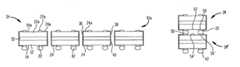
- FIGS. 1A and 1Billustrate a top view and a cross-sectional view, respectively of a wafer or first subassembly 10 .
- a portion of a first wafer or subassembly 10includes a plurality of microelectronic elements 12 , each positioned side by side and adjacent to one another.
- the first subassemblypreferably includes numerous rows of microelectronic elements 12 aligned along an X-axis and a Y-axis in various columns and rows.
- the microelectronic elements 12are formed integral with one another using conventional semiconductor process techniques.
- the present inventionis also applicable to reconstituted wafers.
- Each microelectronic element 12includes a front face 14 and an oppositely-facing rear face 16 .
- the microelectronic elements 12also include first edges 18 , second edges 20 , third edges 19 and fourth edges 21 , all of which extend from the front faces 14 to the rear faces 16 of the microelectronic elements 12 .
- a first edge 18 of one microelectronic element 12is attached to a second edge 20 of a second and adjacent microelectronic element 12 .
- the microelectronic elements 12 positioned within the middle of the first subassembly 10are bordered by an adjacent microelectronic element 12 at all four edges, as shown in FIG. 1A .
- the microelectronic elements 12 positioned at a first end 11 , a second end 13 , a third end 15 or a fourth end 17 of the waferhave at least one edge unencumbered by an additional microelectronic element.
- first wafer/subassembly 10may include any number of microelectronic elements including as little as one or as many as is desirable.
- Each of the microelectronic elements 12 in subassembly 10also include a plurality of contacts 22 exposed at their respective front faces 16 . Further, the contacts 22 are attached to traces 24 that extend from the contacts 22 to an edge of the microelectronic element.
- microelectronic 12 ′includes contact 22 ′ and trace 24 ′, which extends from contact 22 ′ to first edge 18 ′ of the microelectronic element 12 ′.
- microelectronic element 12 ′′includes contact 22 ′′ and trace 24 ′′, which extends from contact 22 ′′ to second edge 20 ′′ of microelectronic element 12 ′′.
- traces 24 ′ and 24 ′′actually are a unitary structure extending between contacts 22 ′ and 22 ′′ of adjacent microelectronic elements 12 ′, 12 ′′.
- traces 24 ′ and 24 ′′meet at the attachment point of microelectronic elements 12 ′ and 12 ′′, or at saw lane 23 ′.
- the first subassembly 10is positioned under a second wafer/subassembly 10 A.
- the second subassembly 10 Ais similarly constructed to the first subassembly 10 , and thus like elements will be given similar character references unless otherwise specified.
- the second assembly 10 Ais inverted such that contacts 22 A exposed at front faces 14 A of microelectronic elements 12 A face in an opposite direction as opposed to contacts 22 of subassembly 10 .
- the rear faces 16 A of subassembly 10 Aface towards the rear faces 16 of subassembly 10 .
- the stacked assembly 30consists of a plurality of microelectronic elements 12 , 12 A, oriented and aligned in various rows and columns.
- an adhesive layer 32is positioned between the rear faces 16 , 16 A and adhered thereto.
- the adhesive layer 32is preferably comprised of an adhesive, epoxy or the like, and once cured, maintains a connection between the two subassemblies 10 , 10 A, such that the subassemblies are attached to one another and form stacked assembly 30 .
- the two subassemblies 10 , 10 Amay be attached using other methods that do not involve the use of an adhesive such as directly attaching the rear faces 16 of the subassembly 10 to the rear faces 16 A of the second subassembly 10 A. For example, solder bonding, eutectic bonding, diffusion bonding or other known bonding procedures can be used.
- the stacked assembly 30is diced to form individual stacked units 34 using a mechanical cutting instrument not shown in the figures. Examples of such a mechanical cutting instrument can be found in U.S. Pat. Nos. 6,646,289 and 6,972,480, the disclosures of which are hereby incorporated by reference herein.
- the stacked assembly 30is diced at locations that correspond to saw lanes 23 , 23 A of the individual subassemblies 10 , 10 A and various edges of the microelectronic elements 12 , 12 A. Since the ends of the traces 24 , 24 A that are remote from the contacts 22 , 22 A are positioned within the saw lanes 23 , 23 A, the dicing of the stacked assembly 30 causes these ends to become exposed.
- Each individual stacked unit 34includes a microelectronic element 12 A disposed above a microelectronic element 12 and attached thereto by adhesive layer 32 .
- the respective front faces 14 , 14 A of the microelectronic elements 12 , 12 Aface in opposite directions as do the contacts 22 , 22 A of respective microelectronic elements.
- the individual stacked units 34include a first side wall 36 and a second side wall 38 that extend between the front faces 14 , 14 A of the microelectronic elements 12 and 12 A. Adjacent to both side walls 36 , 38 are the ends of the traces 24 , 24 A that are exposed after the dicing process.
- a trace bridge 40extends from a trace 40 across either side wall 36 or side wall 38 to a trace 24 A, and thereby electrically interconnects the two traces disposed on opposite faces of individual stacked units 34 .
- the traces bridgesextend about the edges of the microelectronic elements as well as the edges of the adhesive layer 32 that is exposed as a result of the dicing process.
- a contact 22is in electrical communication with a contact 22 A.
- a dielectric layer 41may be disposed onto the exposed edges of the microelectronic elements and adhesive layer so as to electrically isolate the trace bridges from the bodies of the microelectronic elements if desired.
- a mass of conductive material 42may be deposited onto contacts 22 so as to enable the individual stacked units 34 to be electrically connected to a substrate such as a circuit panel and the like.
- the mass of conductive material 42may be a ball of solder or similar material.
- individual stacked units 34 and 34 ′may be stacked one upon another with contacts of individual stacked unit 34 being electrically connected to contacts of individual stacked unit 34 ′ as shown in FIG. 4 .
- the contacts 50 exposed at a lower surface 52 of stacked unit 34is aligned with the contacts 50 ′ exposed at the top surface 54 ′ of stacked unit 34 ′
- the contacts 50 and 50 ′may then be electrically connected using a mass of conductive material 56 such as solder or attached to one another using other methods known to those in the art.
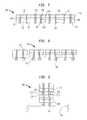
- a subassembly 110 including a plurality of microelectronic elements 112may be provided as shown in FIGS. 5A and 5B .
- Subassembly 110is similarly constructed as subassembly 10 and includes many of the same features. For this reason, like elements will be given similar character references unless otherwise specified.
- the microelectronic elements 112 of subassembly 110include a front face 114 and an oppositely-facing rear face 116 .
- each microelectronic element 112includes a first edge 118 , a second edge 120 , a third edge 119 and a fourth edge 121 extending between the front face 114 and rear face 116 .
- the locationswere one edge of a first microelectronic element abuts an edge of a second microelectronic element forms saw lanes 123 .
- the saw lanesmay be cut there through without damaging the individual microelectronic elements 112 of the subassembly 110 .
- demarcation linesare shown in FIGS. 5A to 5B for clarity of illustration, in practice a clear separation between adjacent microelectronic elements 112 may not be recognizable.
- Each microelectronic element 112also includes a plurality of contacts 122 exposed at their respective front face 114 .
- the subassembly 110is illustrated having four rows and three columns of microelectronic elements, the number of microelectronic elements may be as little as one and as many as is desirable.
- the subassembly 110is subjected to a mechanical cutting process that bores vias 130 through each of the microelectronic elements 112 .
- the viasextend from a rear face 116 to a front face 114 of each of the microelectronic elements.
- each of the vias 130is preferably aligned with a contact 122 exposed on the front face 114 of each of the microelectronic elements 112 such that the contacts 122 are not only exposed at the front faces 114 but also at the rear faces 116 .
- the vias 130are filled with a conductive material 131 such as a metal.
- the conductive material 131may for instance be formed from copper or a copper/gold alloy.
- a stacked assembly 132may be assembled by attaching the first subassembly 110 to a second subassembly 110 ′.
- the second subassembly 110 ′is similarly constructed as subassembly 110 and like features are described using similar character references unless otherwise specified.
- the second subassembly 110 ′is inverted such that the rear faces 116 ′ of the microelectronic elements 112 ′ of the second subassembly face toward the rear faces 116 of microelectronic elements 112 .
- the saw lanes 123 of subassembly 110are aligned with the saw lanes 123 ′ of second subassembly 110 ′ and the vias 130 , 130 ′ of each of the subassemblies are also aligned.
- the vias 130 to the vias 130 ′the contacts 122 of the microelectronic elements 112 are aligned with the contacts 122 ′ of the second subassembly and the conductive material 131 , 131 ′ of each of the vias 130 , 130 ′ are brought proximate to one another.
- a second conductive material 137may be utilized.
- masses of the second conductive material 137such as solder, are disposed in and around the vias 130 proximate the rear faces 116 of the microelectronic elements 112 and in contact with the conductive material 131 contained within the vias.
- the subassembly 110is then brought proximate with the second subassembly 110 ′ such that the second conductive material 137 is proximate vias 130 ′ and in contact with the conductive material 131 ′ of the second subassembly. As shown in FIG.
- this configurationcauses the contacts 122 to be electrically connected to contacts 122 ′ through the various conductive materials disposed within the vias 130 , 130 ′ and thus the conductive material 131 , 131 ′ act as electrical bridges between contacts 122 , 122 ′.
- a back fillsuch as encapsulant material 134 or an adhesive may be positioned between the two subassemblies 110 , 110 ′ to provide additional rigidity to the stacked assembly 132 .
- the conductive material 131 of subassembly 110may be directly adhered to the conductive material 131 ′ of the second subassembly 110 ′.
- the conductive material 130 , 130 ′is copper
- the copper in each via 130 , 130 ′is reflowed and allowed to contact the copper in an aligned via.
- the copper in adjacent vias 130 , 130 ′forms, not only an attachment area between the subassemblies but also an electrical connection between contacts 122 , 122 ′.
- the stacked assembly 132is now ready to be diced into individual stacked units 140 .
- a similar mechanical instrument(not shown in the figures) described previously is brought proximate the saw lanes 123 , 123 ′ of each of the subassemblies 110 , 110 ′.
- the mechanical toolis passed through the stacked assembly 132 at positions that correspond to the saw lanes 123 , 123 ′ thereby dissecting the stacked assembly into individual stacked units 140 .
- a mass of solder 142 or other conductive materialmay be disposed on exposed contacts 122 or 122 ′ so as to enable the individual stacked units 140 to be attached to a substrate such as a circuit panel.
- the stacked assembly 132may also be attached to a circuit panel without having to dice the assembly into individual units if desired.
- individual stacked units 140 and 140 ′may be stacked one upon another with the contacts of individual stacked unit 140 being electrically connected to contacts of individual stacked unit 140 ′.
- the contacts 150 exposed at a lower surface 152 of stacked unit 140are aligned with the contacts 150 ′ exposed at the top surface 154 ′ of stacked unit 140 ′
- the contacts 150 and 150 ′may then be electrically connected using a mass of conductive material 156 such as solder or attached to one another using other methods known to those in the art.
- the entire assembly 160may be attached to a substrate such as circuit panel 170 illustrated in FIG. 9 , which includes conductive pads 172 .
Landscapes
- Engineering & Computer Science (AREA)
- Microelectronics & Electronic Packaging (AREA)
- Power Engineering (AREA)
- Computer Hardware Design (AREA)
- Physics & Mathematics (AREA)
- Condensed Matter Physics & Semiconductors (AREA)
- General Physics & Mathematics (AREA)
- Wire Bonding (AREA)
- Dicing (AREA)
- Cooling Or The Like Of Semiconductors Or Solid State Devices (AREA)
Abstract
Description
Claims (4)
Priority Applications (1)
| Application Number | Priority Date | Filing Date | Title |
|---|---|---|---|
| US13/115,318US8349654B2 (en) | 2006-12-28 | 2011-05-25 | Method of fabricating stacked packages with bridging traces |
Applications Claiming Priority (2)
| Application Number | Priority Date | Filing Date | Title |
|---|---|---|---|
| US11/648,172US7952195B2 (en) | 2006-12-28 | 2006-12-28 | Stacked packages with bridging traces |
| US13/115,318US8349654B2 (en) | 2006-12-28 | 2011-05-25 | Method of fabricating stacked packages with bridging traces |
Related Parent Applications (1)
| Application Number | Title | Priority Date | Filing Date |
|---|---|---|---|
| US11/648,172DivisionUS7952195B2 (en) | 2006-12-28 | 2006-12-28 | Stacked packages with bridging traces |
Publications (2)
| Publication Number | Publication Date |
|---|---|
| US20110230013A1 US20110230013A1 (en) | 2011-09-22 |
| US8349654B2true US8349654B2 (en) | 2013-01-08 |
Family
ID=39488194
Family Applications (2)
| Application Number | Title | Priority Date | Filing Date |
|---|---|---|---|
| US11/648,172Active2028-08-23US7952195B2 (en) | 2006-12-28 | 2006-12-28 | Stacked packages with bridging traces |
| US13/115,318ActiveUS8349654B2 (en) | 2006-12-28 | 2011-05-25 | Method of fabricating stacked packages with bridging traces |
Family Applications Before (1)
| Application Number | Title | Priority Date | Filing Date |
|---|---|---|---|
| US11/648,172Active2028-08-23US7952195B2 (en) | 2006-12-28 | 2006-12-28 | Stacked packages with bridging traces |
Country Status (6)
| Country | Link |
|---|---|
| US (2) | US7952195B2 (en) |
| EP (1) | EP2097925B1 (en) |
| JP (1) | JP5567346B2 (en) |
| KR (1) | KR101454332B1 (en) |
| CN (1) | CN101595562B (en) |
| WO (1) | WO2008085391A2 (en) |
Families Citing this family (37)
| Publication number | Priority date | Publication date | Assignee | Title |
|---|---|---|---|---|
| US7901989B2 (en) | 2006-10-10 | 2011-03-08 | Tessera, Inc. | Reconstituted wafer level stacking |
| US8513789B2 (en) | 2006-10-10 | 2013-08-20 | Tessera, Inc. | Edge connect wafer level stacking with leads extending along edges |
| US7829438B2 (en) | 2006-10-10 | 2010-11-09 | Tessera, Inc. | Edge connect wafer level stacking |
| US7759166B2 (en)* | 2006-10-17 | 2010-07-20 | Tessera, Inc. | Microelectronic packages fabricated at the wafer level and methods therefor |
| US7952195B2 (en)* | 2006-12-28 | 2011-05-31 | Tessera, Inc. | Stacked packages with bridging traces |
| US8723332B2 (en)* | 2007-06-11 | 2014-05-13 | Invensas Corporation | Electrically interconnected stacked die assemblies |
| JP5572089B2 (en) | 2007-07-27 | 2014-08-13 | テッセラ,インコーポレイテッド | Reconfigured wafer stack packaging with pad extension after application |
| US8551815B2 (en) | 2007-08-03 | 2013-10-08 | Tessera, Inc. | Stack packages using reconstituted wafers |
| US8043895B2 (en) | 2007-08-09 | 2011-10-25 | Tessera, Inc. | Method of fabricating stacked assembly including plurality of stacked microelectronic elements |
| WO2009035849A2 (en) | 2007-09-10 | 2009-03-19 | Vertical Circuits, Inc. | Semiconductor die mount by conformal die coating |
| CN101999167B (en) | 2008-03-12 | 2013-07-17 | 伊文萨思公司 | Support mounted electrically interconnected die assembly |
| US7863159B2 (en) | 2008-06-19 | 2011-01-04 | Vertical Circuits, Inc. | Semiconductor die separation method |
| US9153517B2 (en) | 2008-05-20 | 2015-10-06 | Invensas Corporation | Electrical connector between die pad and z-interconnect for stacked die assemblies |
| JP5639052B2 (en) | 2008-06-16 | 2014-12-10 | テッセラ,インコーポレイテッド | Edge stacking at wafer level |
| WO2010104610A2 (en) | 2009-03-13 | 2010-09-16 | Tessera Technologies Hungary Kft. | Stacked microelectronic assemblies having vias extending through bond pads |
| WO2010151578A2 (en) | 2009-06-26 | 2010-12-29 | Vertical Circuits, Inc. | Electrical interconnect for die stacked in zig-zag configuration |
| JP5425584B2 (en)* | 2009-10-15 | 2014-02-26 | ルネサスエレクトロニクス株式会社 | Manufacturing method of semiconductor device |
| WO2011056668A2 (en) | 2009-10-27 | 2011-05-12 | Vertical Circuits, Inc. | Selective die electrical insulation additive process |
| US7915083B1 (en)* | 2009-10-28 | 2011-03-29 | Headway Technologies, Inc. | Method of manufacturing layered chip package |
| TWI544604B (en) | 2009-11-04 | 2016-08-01 | 英維瑟斯公司 | Stacked die assembly having reduced stress electrical interconnects |
| US8541887B2 (en) | 2010-09-03 | 2013-09-24 | Headway Technologies, Inc. | Layered chip package and method of manufacturing same |
| US8441112B2 (en)* | 2010-10-01 | 2013-05-14 | Headway Technologies, Inc. | Method of manufacturing layered chip package |
| US8618646B2 (en)* | 2010-10-12 | 2013-12-31 | Headway Technologies, Inc. | Layered chip package and method of manufacturing same |
| US8652877B2 (en) | 2010-12-06 | 2014-02-18 | Headway Technologies, Inc. | Method of manufacturing layered chip package |
| US8653639B2 (en)* | 2011-06-09 | 2014-02-18 | Headway Technologies, Inc. | Layered chip package and method of manufacturing same |
| US9007520B2 (en) | 2012-08-10 | 2015-04-14 | Nanchang O-Film Optoelectronics Technology Ltd | Camera module with EMI shield |
| US9001268B2 (en) | 2012-08-10 | 2015-04-07 | Nan Chang O-Film Optoelectronics Technology Ltd | Auto-focus camera module with flexible printed circuit extension |
| US9242602B2 (en) | 2012-08-27 | 2016-01-26 | Fotonation Limited | Rearview imaging systems for vehicle |
| KR102190382B1 (en)* | 2012-12-20 | 2020-12-11 | 삼성전자주식회사 | Semiconductor package |
| US9241400B2 (en) | 2013-08-23 | 2016-01-19 | Seagate Technology Llc | Windowed reference planes for embedded conductors |
| US9825002B2 (en) | 2015-07-17 | 2017-11-21 | Invensas Corporation | Flipped die stack |
| US9490195B1 (en) | 2015-07-17 | 2016-11-08 | Invensas Corporation | Wafer-level flipped die stacks with leadframes or metal foil interconnects |
| US9871019B2 (en) | 2015-07-17 | 2018-01-16 | Invensas Corporation | Flipped die stack assemblies with leadframe interconnects |
| US9508691B1 (en) | 2015-12-16 | 2016-11-29 | Invensas Corporation | Flipped die stacks with multiple rows of leadframe interconnects |
| US10566310B2 (en) | 2016-04-11 | 2020-02-18 | Invensas Corporation | Microelectronic packages having stacked die and wire bond interconnects |
| US9595511B1 (en) | 2016-05-12 | 2017-03-14 | Invensas Corporation | Microelectronic packages and assemblies with improved flyby signaling operation |
| US9728524B1 (en) | 2016-06-30 | 2017-08-08 | Invensas Corporation | Enhanced density assembly having microelectronic packages mounted at substantial angle to board |
Citations (227)
| Publication number | Priority date | Publication date | Assignee | Title |
|---|---|---|---|---|
| US4074342A (en) | 1974-12-20 | 1978-02-14 | International Business Machines Corporation | Electrical package for lsi devices and assembly process therefor |
| US4500905A (en) | 1981-09-30 | 1985-02-19 | Tokyo Shibaura Denki Kabushiki Kaisha | Stacked semiconductor device with sloping sides |
| JPS60160645A (en) | 1984-02-01 | 1985-08-22 | Hitachi Ltd | Laminated semiconductor integrated circuit device |
| US4765864A (en) | 1987-07-15 | 1988-08-23 | Sri International | Etching method for producing an electrochemical cell in a crystalline substrate |
| US4842699A (en) | 1988-05-10 | 1989-06-27 | Avantek, Inc. | Method of selective via-hole and heat sink plating using a metal mask |
| US4897708A (en) | 1986-07-17 | 1990-01-30 | Laser Dynamics, Inc. | Semiconductor wafer array |
| US4954875A (en) | 1986-07-17 | 1990-09-04 | Laser Dynamics, Inc. | Semiconductor wafer array with electrically conductive compliant material |
| US5322816A (en) | 1993-01-19 | 1994-06-21 | Hughes Aircraft Company | Method for forming deep conductive feedthroughs |
| US5343071A (en) | 1993-04-28 | 1994-08-30 | Raytheon Company | Semiconductor structures having dual surface via holes |
| FR2704690A1 (en) | 1993-04-27 | 1994-11-04 | Thomson Csf | Method for encapsulating semiconductor wafers, device obtained by this process and application to the interconnection of wafers in three dimensions. |
| US5412539A (en) | 1993-10-18 | 1995-05-02 | Hughes Aircraft Company | Multichip module with a mandrel-produced interconnecting decal |
| US5424245A (en) | 1994-01-04 | 1995-06-13 | Motorola, Inc. | Method of forming vias through two-sided substrate |
| US5426072A (en) | 1993-01-21 | 1995-06-20 | Hughes Aircraft Company | Process of manufacturing a three dimensional integrated circuit from stacked SOI wafers using a temporary silicon substrate |
| US5466634A (en) | 1994-12-20 | 1995-11-14 | International Business Machines Corporation | Electronic modules with interconnected surface metallization layers and fabrication methods therefore |
| US5563084A (en) | 1994-09-22 | 1996-10-08 | Fraunhofer-Gesellschaft zur F orderung der angewandten Forschung e.V. | Method of making a three-dimensional integrated circuit |
| US5571754A (en) | 1995-07-26 | 1996-11-05 | International Business Machines Corporation | Method of fabrication of endcap chip with conductive, monolithic L-connect for multichip stack |
| US5604673A (en) | 1995-06-07 | 1997-02-18 | Hughes Electronics | Low temperature co-fired ceramic substrates for power converters |
| US5608264A (en) | 1995-06-05 | 1997-03-04 | Harris Corporation | Surface mountable integrated circuit with conductive vias |
| US5614766A (en) | 1991-09-30 | 1997-03-25 | Rohm Co., Ltd. | Semiconductor device with stacked alternate-facing chips |
| US5618752A (en) | 1995-06-05 | 1997-04-08 | Harris Corporation | Method of fabrication of surface mountable integrated circuits |
| US5646067A (en) | 1995-06-05 | 1997-07-08 | Harris Corporation | Method of bonding wafers having vias including conductive material |
| US5656553A (en) | 1994-08-22 | 1997-08-12 | International Business Machines Corporation | Method for forming a monolithic electronic module by dicing wafer stacks |
| US5661087A (en) | 1994-06-23 | 1997-08-26 | Cubic Memory, Inc. | Vertical interconnect process for silicon segments |
| US5682062A (en) | 1995-06-05 | 1997-10-28 | Harris Corporation | System for interconnecting stacked integrated circuits |
| US5716759A (en) | 1993-09-02 | 1998-02-10 | Shellcase Ltd. | Method and apparatus for producing integrated circuit devices |
| US5767001A (en) | 1993-05-05 | 1998-06-16 | Siemens Aktiengesellschaft | Process for producing semiconductor components between which contact is made vertically |
| US5766984A (en) | 1994-09-22 | 1998-06-16 | Fraunhofer-Gesellschaft Zur Foerderung Der Angewandten Forschung | Method of making a vertical integrated circuit |
| US5804004A (en) | 1992-05-11 | 1998-09-08 | Nchip, Inc. | Stacked devices for multichip modules |
| US5814889A (en) | 1995-06-05 | 1998-09-29 | Harris Corporation | Intergrated circuit with coaxial isolation and method |
| US5817530A (en) | 1996-05-20 | 1998-10-06 | Micron Technology, Inc. | Use of conductive lines on the back side of wafers and dice for semiconductor interconnects |
| WO1998045130A1 (en) | 1997-04-04 | 1998-10-15 | Leedy Glenn J | Three dimensional structure memory |
| US5880010A (en) | 1994-07-12 | 1999-03-09 | Sun Microsystems, Inc. | Ultrathin electronics |
| EP0926723A1 (en) | 1997-11-26 | 1999-06-30 | STMicroelectronics S.r.l. | Process for forming front-back through contacts in micro-integrated electronic devices |
| WO1999040624A1 (en) | 1998-02-06 | 1999-08-12 | Shellcase Ltd. | Integrated circuit device |
| US5946545A (en) | 1994-03-30 | 1999-08-31 | Internatinal Business Machines Corporation | Semiconductor stack structures and fabrication/sparing methods utilizing programmable spare circuit |
| US5973386A (en) | 1996-02-16 | 1999-10-26 | Nec Corporation | Semiconductor substrate having silicon oxide layers formed between polysilicon layers |
| US6022758A (en) | 1994-07-10 | 2000-02-08 | Shellcase Ltd. | Process for manufacturing solder leads on a semiconductor device package |
| US6031274A (en) | 1996-10-11 | 2000-02-29 | Hamamatsu Photonics K.K. | Back irradiation type light-receiving device and method of making the same |
| US6040235A (en) | 1994-01-17 | 2000-03-21 | Shellcase Ltd. | Methods and apparatus for producing integrated circuit devices |
| US6103552A (en) | 1998-08-10 | 2000-08-15 | Lin; Mou-Shiung | Wafer scale packaging scheme |
| EP1041624A1 (en) | 1999-04-02 | 2000-10-04 | Interuniversitair Microelektronica Centrum Vzw | Method of transferring ultra-thin substrates and application of the method to the manufacture of a multilayer thin film device |
| US6130823A (en) | 1999-02-01 | 2000-10-10 | Raytheon E-Systems, Inc. | Stackable ball grid array module and method |
| US6177721B1 (en) | 1998-10-21 | 2001-01-23 | Hyundai Electronics Industries Co., Ltd | Chip stack-type semiconductor package and method for fabricating the same |
| US6177707B1 (en) | 1998-03-02 | 2001-01-23 | U.S. Philips Corporation | Semiconductor device comprising a glass supporting body onto which a substrate with semiconductor elements and a metalization is attached by means of an adhesive |
| JP2001035995A (en) | 1999-07-22 | 2001-02-09 | Seiko Epson Corp | Method for forming through hole in semiconductor chip |
| US6188129B1 (en) | 1997-03-24 | 2001-02-13 | Hyundai Electronics Industries Co., Ltd. | Stacked semiconductor chip package having external terminal pads and stackable chips having a protection layer |
| US6204562B1 (en) | 1999-02-11 | 2001-03-20 | United Microelectronics Corp. | Wafer-level chip scale package |
| US6228686B1 (en) | 1995-09-18 | 2001-05-08 | Tessera, Inc. | Method of fabricating a microelectronic assembly using sheets with gaps to define lead regions |
| US6261865B1 (en) | 1998-10-06 | 2001-07-17 | Micron Technology, Inc. | Multi chip semiconductor package and method of construction |
| JP2001217386A (en) | 2000-02-03 | 2001-08-10 | Seiko Epson Corp | Semiconductor device, method of manufacturing the same, and electronic device |
| US6277669B1 (en) | 1999-09-15 | 2001-08-21 | Industrial Technology Research Institute | Wafer level packaging method and packages formed |
| US20010024839A1 (en) | 1998-12-17 | 2001-09-27 | Lin Charles Wen Chyang | Bumpless flip chip assembly with strips-in-via and plating |
| US6340845B1 (en) | 1999-01-22 | 2002-01-22 | Nec Corporation | Memory package implementing two-fold memory capacity and two different memory functions |
| US6344401B1 (en) | 2000-03-09 | 2002-02-05 | Atmel Corporation | Method of forming a stacked-die integrated circuit chip package on a water level |
| US20020047199A1 (en) | 2000-09-11 | 2002-04-25 | Shinji Ohuchi | Semiconductor device, manufacturing method of semiconductor device, stack type semiconductor device, and manufacturing method of stack type semiconductor device |
| US6396710B1 (en) | 2000-05-12 | 2002-05-28 | Raytheon Company | High density interconnect module |
| US20020074637A1 (en) | 2000-12-19 | 2002-06-20 | Intel Corporation | Stacked flip chip assemblies |
| US20020109236A1 (en) | 2001-02-09 | 2002-08-15 | Samsung Electronics Co., Ltd. | Three-dimensional multi-chip package having chip selection pads and manufacturing method thereof |
| US20020113303A1 (en) | 2000-12-18 | 2002-08-22 | Kei Murayama | Mounting structure for semiconductor devices |
| US20020127775A1 (en) | 1999-12-23 | 2002-09-12 | Rambus Inc. | Redistributed bond pads in stacked integrated circuit die package |
| US20020132465A1 (en) | 1997-04-04 | 2002-09-19 | Elm Technology Corporation | Reconfigurable integrated circuit memory |
| US6472293B2 (en) | 1999-04-13 | 2002-10-29 | Oki Electric Industry Co., Ltd. | Method for manufacturing an interconnect structure for stacked semiconductor device |
| US6472247B1 (en) | 2000-06-26 | 2002-10-29 | Ricoh Company, Ltd. | Solid-state imaging device and method of production of the same |
| US20020171145A1 (en) | 2001-05-21 | 2002-11-21 | Akifumi Higuchi | BGA type semiconductor device, tape carrier for semiconductor device, and semiconductor device using said tape carrier |
| US6492201B1 (en) | 1998-07-10 | 2002-12-10 | Tessera, Inc. | Forming microelectronic connection components by electrophoretic deposition |
| US6498381B2 (en) | 2001-02-22 | 2002-12-24 | Tru-Si Technologies, Inc. | Semiconductor structures having multiple conductive layers in an opening, and methods for fabricating same |
| US6498387B1 (en) | 2000-02-15 | 2002-12-24 | Wen-Ken Yang | Wafer level package and the process of the same |
| US20030006494A1 (en) | 2001-07-03 | 2003-01-09 | Lee Sang Ho | Thin profile stackable semiconductor package and method for manufacturing |
| JP2003037758A (en) | 2001-01-12 | 2003-02-07 | Konica Corp | Imaging device |
| US6548391B1 (en) | 1999-05-27 | 2003-04-15 | Fraunhofer-Gesellschaft Zur Foerderung Der Angewandten Forschung E. V. | Method of vertically integrating electric components by means of back contacting |
| US6562653B1 (en) | 1999-01-11 | 2003-05-13 | Intel Corporation | Silicon interposer and multi-chip-module (MCM) with through substrate vias |
| US20030094683A1 (en) | 2001-11-16 | 2003-05-22 | Poo Chia Yong | Stackable semiconductor package and wafer level fabrication method |
| US6582991B1 (en) | 2000-12-14 | 2003-06-24 | Matsushita Electric Industrial Co., Ltd. | Semiconductor device and method for fabricating the same |
| JP2003208655A (en) | 2002-01-16 | 2003-07-25 | Hitachi Ltd | Automatic transaction equipment |
| US6608377B2 (en) | 2001-01-30 | 2003-08-19 | Samsung Electronics Co., Ltd. | Wafer level package including ground metal layer |
| US6607941B2 (en) | 2002-01-11 | 2003-08-19 | National Semiconductor Corporation | Process and structure improvements to shellcase style packaging technology |
| US6607938B2 (en) | 2001-07-19 | 2003-08-19 | Samsung Electronics Co., Ltd. | Wafer level stack chip package and method for manufacturing same |
| US6621155B1 (en) | 1999-12-23 | 2003-09-16 | Rambus Inc. | Integrated circuit device having stacked dies and impedance balanced transmission lines |
| US6624505B2 (en) | 1998-02-06 | 2003-09-23 | Shellcase, Ltd. | Packaged integrated circuits and methods of producing thereof |
| US20030209772A1 (en) | 2002-05-13 | 2003-11-13 | National Semiconductor Corporation | Electrical die contact structure and fabrication method |
| US6656827B1 (en) | 2002-10-17 | 2003-12-02 | Taiwan Semiconductor Manufacturing Co., Ltd. | Electrical performance enhanced wafer level chip scale package with ground |
| US20030233704A1 (en) | 2000-04-17 | 2003-12-25 | Miguel Castellote | Air massage system for bathtub |
| US20040014255A1 (en) | 2002-07-22 | 2004-01-22 | Grigg Ford B. | Thick solder mask for confining encapsulant material over selected locations of a substrate, assemblies including the solder mask, and methods |
| US20040016942A1 (en) | 2002-04-24 | 2004-01-29 | Seiko Epson Corporation | Semiconductor device and a method of manufacturing the same, a circuit board and an electronic apparatus |
| US6693358B2 (en) | 2000-10-23 | 2004-02-17 | Matsushita Electric Industrial Co., Ltd. | Semiconductor chip, wiring board and manufacturing process thereof as well as semiconductor device |
| JP2004063569A (en) | 2002-07-25 | 2004-02-26 | Seiko Epson Corp | Semiconductor device and its manufacturing method, circuit board, and electronic equipment |
| WO2004025727A1 (en) | 2002-09-10 | 2004-03-25 | Frank Niklaus | Method for sealing a microcavity and package comprising at least one microcavity |
| US6717254B2 (en) | 2001-02-22 | 2004-04-06 | Tru-Si Technologies, Inc. | Devices having substrates with opening passing through the substrates and conductors in the openings, and methods of manufacture |
| US6727576B2 (en) | 2001-10-31 | 2004-04-27 | Infineon Technologies Ag | Transfer wafer level packaging |
| US20040082114A1 (en) | 2002-10-29 | 2004-04-29 | Chih-Horng Horng | Fabrication method of window-type ball grid array semiconductor package |
| US6737300B2 (en) | 2001-01-24 | 2004-05-18 | Advanced Semiconductor Engineering, Inc. | Chip scale package and manufacturing method |
| US6743660B2 (en) | 2002-01-12 | 2004-06-01 | Taiwan Semiconductor Manufacturing Co., Ltd | Method of making a wafer level chip scale package |
| US20040104454A1 (en) | 2002-10-10 | 2004-06-03 | Rohm Co., Ltd. | Semiconductor device and method of producing the same |
| US6753205B2 (en) | 2001-09-13 | 2004-06-22 | Tru-Si Technologies, Inc. | Method for manufacturing a structure comprising a substrate with a cavity and a semiconductor integrated circuit bonded to a contact pad located in the cavity |
| US6753208B1 (en) | 1998-03-20 | 2004-06-22 | Mcsp, Llc | Wafer scale method of packaging integrated circuit die |
| US20040142509A1 (en) | 2002-09-24 | 2004-07-22 | Seiko Epson Corporation | Semiconductor device and method of manufacturing the same, circuit board, and electronic instrument |
| US20040155354A1 (en) | 2000-06-02 | 2004-08-12 | Seiko Epson Corporation | Semiconductor device, method of fabricating the same, stack-type semiconductor device, circuit board and electronic instrument |
| US6777767B2 (en) | 1999-12-10 | 2004-08-17 | Shellcase Ltd. | Methods for producing packaged integrated circuit devices & packaged integrated circuit devices produced thereby |
| US6784023B2 (en)* | 1996-05-20 | 2004-08-31 | Micron Technology, Inc. | Method of fabrication of stacked semiconductor devices |
| US20040169278A1 (en) | 2001-05-21 | 2004-09-02 | Kinsman Larry D. | Bumped die and wire bonded board-on-chip package |
| US6806559B2 (en) | 2002-04-22 | 2004-10-19 | Irvine Sensors Corporation | Method and apparatus for connecting vertically stacked integrated circuit chips |
| US20040222508A1 (en) | 2003-03-18 | 2004-11-11 | Akiyoshi Aoyagi | Semiconductor device, electronic device, electronic apparatus, method of manufacturing semiconductor device, and method of manufacturing electronic device |
| US20040221451A1 (en) | 2003-05-06 | 2004-11-11 | Micron Technology, Inc. | Method for packaging circuits and packaged circuits |
| EP1482553A2 (en) | 2003-05-26 | 2004-12-01 | Sanyo Electric Co., Ltd. | Semiconductor device and manufacturing method thereof |
| US6828175B2 (en) | 2002-08-29 | 2004-12-07 | Micron Technology, Inc. | Semiconductor component with backside contacts and method of fabrication |
| US20040251525A1 (en) | 2003-06-16 | 2004-12-16 | Shellcase Ltd. | Methods and apparatus for packaging integrated circuit devices |
| WO2004114397A1 (en) | 2003-06-20 | 2004-12-29 | Koninklijke Philips Electronics N.V. | Electronic device, assembly and methods of manufacturing an electronic device |
| US20050003649A1 (en) | 2003-06-09 | 2005-01-06 | Sanyo Electric Co., Ltd. | Semiconductor device and manufacturing method thereof |
| US6844619B2 (en) | 2000-12-01 | 2005-01-18 | Nec Corporation | Compact semiconductor device capable of mounting a plurality of semiconductor chips with high density and method of manufacturing the same |
| US20050012225A1 (en) | 2002-11-15 | 2005-01-20 | Choi Seung-Yong | Wafer-level chip scale package and method for fabricating and using the same |
| US20050046002A1 (en) | 2003-08-26 | 2005-03-03 | Kang-Wook Lee | Chip stack package and manufacturing method thereof |
| US6864172B2 (en) | 2002-06-18 | 2005-03-08 | Sanyo Electric Co., Ltd. | Manufacturing method of semiconductor device |
| US6867123B2 (en) | 2001-02-08 | 2005-03-15 | Renesas Technology Corp. | Semiconductor integrated circuit device and its manufacturing method |
| US20050056903A1 (en) | 2003-08-28 | 2005-03-17 | Satoshi Yamamoto | Semiconductor package and method of manufacturing same |
| US6870249B2 (en) | 2002-12-24 | 2005-03-22 | Oki Electric Industry Co., Ltd. | Semiconductor device and manufacturing method thereof |
| EP1519410A1 (en) | 2003-09-25 | 2005-03-30 | Interuniversitair Microelektronica Centrum vzw ( IMEC) | Method for producing electrical through hole interconnects and devices made thereof |
| US20050067680A1 (en) | 2003-09-30 | 2005-03-31 | Boon Suan Jeung | Castellated chip-scale packages and methods for fabricating the same |
| US20050073035A1 (en) | 2003-09-19 | 2005-04-07 | Moxham Stephen F. | Semiconductor component having stiffener and circuit decal and method of fabrication |
| US6878608B2 (en) | 2001-05-31 | 2005-04-12 | International Business Machines Corporation | Method of manufacture of silicon based package |
| JP2005101067A (en) | 2003-09-22 | 2005-04-14 | Sharp Corp | Substrate wiring structure and wiring forming method |
| US20050095835A1 (en) | 2003-09-26 | 2005-05-05 | Tessera, Inc. | Structure and method of making capped chips having vertical interconnects |
| US20050104179A1 (en) | 2003-07-03 | 2005-05-19 | Shellcase Ltd. | Methods and apparatus for packaging integrated circuit devices |
| US6897148B2 (en) | 2003-04-09 | 2005-05-24 | Tru-Si Technologies, Inc. | Electroplating and electroless plating of conductive materials into openings, and structures obtained thereby |
| US20050156330A1 (en) | 2004-01-21 | 2005-07-21 | Harris James M. | Through-wafer contact to bonding pad |
| DE102004039906A1 (en) | 2004-08-18 | 2005-08-18 | Infineon Technologies Ag | Electronic component with a number of integrated members, is formed by producing members with a surface that contains a circuit, and connecting components using bond wires |
| WO2005081315A2 (en) | 2004-02-18 | 2005-09-01 | Infineon Technologies Ag | Semiconductor component comprising a stack of semiconductor chips and method for producing the same |
| JP2005303031A (en) | 2004-04-13 | 2005-10-27 | Matsushita Electric Ind Co Ltd | Electronic circuit module, multilayer electronic circuit module, and method for manufacturing the same |
| US20050260794A1 (en) | 2002-09-03 | 2005-11-24 | Industrial Technology Research Institute | Method for fabrication of wafer level package incorporating dual compliant layers |
| US20050263866A1 (en) | 2004-05-27 | 2005-12-01 | Chang-Fegn Wan | Hermetic pacakging and method of manufacture and use therefore |
| US6972483B1 (en) | 2004-06-30 | 2005-12-06 | Hynix Semiconductor Inc. | Semiconductor package with improved thermal emission property |
| US20050287783A1 (en) | 2004-06-29 | 2005-12-29 | Kirby Kyle K | Microelectronic devices and methods for forming interconnects in microelectronic devices |
| US6984885B1 (en) | 2000-02-10 | 2006-01-10 | Renesas Technology Corp. | Semiconductor device having densely stacked semiconductor chips |
| US20060006488A1 (en) | 2004-06-30 | 2006-01-12 | Sony Corporation | Solid-state imaging device, camera and method of producing the solid-state imaging device |
| EP1619722A1 (en) | 2003-04-16 | 2006-01-25 | Hamamatsu Photonics K. K. | Method for manufacturing backside-illuminated optical sensor |
| US20060017161A1 (en) | 2004-07-22 | 2006-01-26 | Jae-Sik Chung | Semiconductor package having protective layer for re-routing lines and method of manufacturing the same |
| US20060043598A1 (en) | 2004-08-31 | 2006-03-02 | Kirby Kyle K | Methods of manufacture of a via structure comprising a plurality of conductive elements, semiconductor die, multichip module, and system including same |
| US20060046471A1 (en) | 2004-08-27 | 2006-03-02 | Kirby Kyle K | Methods for forming vias of varying lateral dimensions and semiconductor components and assemblies including same |
| US20060043556A1 (en) | 2004-08-25 | 2006-03-02 | Chao-Yuan Su | Stacked packaging methods and structures |
| US20060046348A1 (en) | 2004-09-01 | 2006-03-02 | Kang Byoung Y | Semiconductor chip packages and methods for fabricating the same |
| US20060043601A1 (en) | 2002-11-14 | 2006-03-02 | Wolfgang Pahl | Hermetically encapsulated component and waferscale method for the production thereof |
| US20060055050A1 (en) | 2004-09-10 | 2006-03-16 | Hideo Numata | Semiconductor device and manufacturing method thereof |
| US20060055061A1 (en) | 2004-09-02 | 2006-03-16 | Ryuji Hosokawa | Semiconductor device and a method of assembling a semiconductor device |
| US20060068580A1 (en) | 2004-09-28 | 2006-03-30 | Sharp Kabushiki Kaisha | Semiconductor device and fabrication method thereof |
| US20060079019A1 (en) | 2004-10-08 | 2006-04-13 | Easetech Korea Co., Ltd. | Method for manufacturing wafer level chip scale package using redistribution substrate |
| US20060076670A1 (en) | 2004-10-08 | 2006-04-13 | Lim Ohk K | Micro-electro-mechanical system (MEMS) package having metal sealing member |
| US7034401B2 (en) | 2003-12-17 | 2006-04-25 | Tru-Si Technologies, Inc. | Packaging substrates for integrated circuits and soldering methods |
| EP1653510A2 (en) | 2004-10-28 | 2006-05-03 | Sanyo Electric Co., Ltd. | Semiconductor device and manufacturing method of the same |
| US20060094165A1 (en) | 2004-10-29 | 2006-05-04 | Harry Hedler | Method for fabricating semiconductor components |
| US7049170B2 (en) | 2003-12-17 | 2006-05-23 | Tru-Si Technologies, Inc. | Integrated circuits and packaging substrates with cavities, and attachment methods including insertion of protruding contact pads into cavities |
| US20060115932A1 (en) | 1997-12-18 | 2006-06-01 | Farnworth Warren M | Method for fabricating semiconductor components with conductive vias |
| US20060138626A1 (en) | 2004-12-29 | 2006-06-29 | Tessera, Inc. | Microelectronic packages using a ceramic substrate having a window and a conductive surface region |
| EP1686627A1 (en) | 2005-01-28 | 2006-08-02 | Samsung Electro-Mechanics Co., Ltd. | Semiconductor package and method of manufacturing the same |
| US7087459B2 (en) | 2002-12-30 | 2006-08-08 | Dongbu Electronics Co., Ltd. | Method for packaging a multi-chip module of a semiconductor device |
| US20060175697A1 (en) | 2005-02-02 | 2006-08-10 | Tetsuya Kurosawa | Semiconductor device having semiconductor chips stacked and mounted thereon and manufacturing method thereof |
| US7115986B2 (en) | 2001-05-02 | 2006-10-03 | Micron Technology, Inc. | Flexible ball grid array chip scale packages |
| US20060220234A1 (en) | 2005-03-22 | 2006-10-05 | Tessera, Inc. | Wire bonded wafer level cavity package |
| US20060220262A1 (en) | 2005-04-04 | 2006-10-05 | Torsten Meyer | Stacked die package |
| US20060249829A1 (en) | 2005-04-08 | 2006-11-09 | Mitsuaki Katagiri | Stacked type semiconductor device |
| US20060258044A1 (en) | 2005-05-11 | 2006-11-16 | Infineon Technologies Ag | Method of manufacturing a semiconductor device comprising stacked chips and a corresponding semiconductor device |
| US20060292866A1 (en) | 2005-06-23 | 2006-12-28 | Borwick Robert L | Low temperature method for fabricating high-aspect ratio vias and devices fabricated by said method |
| US7160753B2 (en) | 2004-03-16 | 2007-01-09 | Voxtel, Inc. | Silicon-on-insulator active pixel sensors |
| EP1741668A2 (en) | 2005-07-05 | 2007-01-10 | Shinko Electric Industries Co., Ltd. | Method for encasing a MEMS device and packaged device |
| US20070007556A1 (en) | 2003-07-23 | 2007-01-11 | Hamamatsu Photonics K.K. | Backside-illuminated photodetector |
| US20070035001A1 (en) | 2005-08-11 | 2007-02-15 | Jochen Kuhmann | Chip scale package for a micro component |
| US20070045862A1 (en) | 2005-09-01 | 2007-03-01 | Micron Technology, Inc. | Stacked microelectronic devices and methods for manufacturing microelectronic devices |
| US20070045803A1 (en) | 2005-08-26 | 2007-03-01 | Micron Technology, Inc. | Microelectronic device packages, stacked microelectronic device packages, and methods for manufacturing microelectronic devices |
| US20070052050A1 (en) | 2005-09-07 | 2007-03-08 | Bart Dierickx | Backside thinned image sensor with integrated lens stack |
| US7215018B2 (en) | 2004-04-13 | 2007-05-08 | Vertical Circuits, Inc. | Stacked die BGA or LGA component assembly |
| US20070102802A1 (en) | 2003-09-19 | 2007-05-10 | Samsung Electronics Co., Ltd. | Single chip and stack-type chip semiconductor package and method of manufacturing the same |
| US20070126085A1 (en) | 2005-12-02 | 2007-06-07 | Nec Electronics Corporation | Semiconductor device and method of manufacturing the same |
| WO2007066409A1 (en) | 2005-12-09 | 2007-06-14 | Spansion Llc | Semiconductor device and its manufacturing method |
| US20070132082A1 (en) | 2005-12-12 | 2007-06-14 | Intel Corporation | Copper plating connection for multi-die stack in substrate package |
| EP1801866A2 (en) | 2002-11-05 | 2007-06-27 | Shinko Electric Industries Co., Ltd. | Semiconductor device and method of manufacturing the same |
| US20070148941A1 (en) | 2005-12-27 | 2007-06-28 | Tessera, Inc. | Microelectronic component with photo-imageable substrate |
| US20070158807A1 (en) | 2005-12-29 | 2007-07-12 | Daoqiang Lu | Edge interconnects for die stacking |
| US20070181989A1 (en) | 2006-02-08 | 2007-08-09 | Micron Technology, Inc. | Microelectronic devices, stacked microelectronic devices, and methods for manufacturing such devices |
| US20070190747A1 (en) | 2006-01-23 | 2007-08-16 | Tessera Technologies Hungary Kft. | Wafer level packaging to lidded chips |
| US7285865B2 (en) | 2005-07-15 | 2007-10-23 | Samsung Electronic Co., Ltd. | Micro-package, multi-stack micro-package, and manufacturing method therefor |
| US20070257350A1 (en) | 2003-11-19 | 2007-11-08 | Kang-Wook Lee | Wafer level stack structure for system-in-package and method thereof |
| US7312521B2 (en) | 2002-04-23 | 2007-12-25 | Sanyo Electric Co., Ltd. | Semiconductor device with holding member |
| US20080083976A1 (en) | 2006-10-10 | 2008-04-10 | Tessera, Inc. | Edge connect wafer level stacking |
| US20080083977A1 (en) | 2006-10-10 | 2008-04-10 | Tessera, Inc. | Edge connect wafer level stacking |
| US20080090333A1 (en) | 2006-10-17 | 2008-04-17 | Tessera, Inc. | Microelectronic packages fabricated at the wafer level and methods therefor |
| US20080099907A1 (en) | 2006-10-31 | 2008-05-01 | Tessera Technologies Hungary Kft. | Wafer-level fabrication of lidded chips with electrodeposited dielectric coating |
| US20080099900A1 (en) | 2006-10-31 | 2008-05-01 | Tessera Technologies Hungary Kft. | Wafer-level fabrication of lidded chips with electrodeposited dielectric coating |
| US20080116545A1 (en) | 2006-11-22 | 2008-05-22 | Tessera, Inc. | Packaged semiconductor chips |
| US20080116544A1 (en) | 2006-11-22 | 2008-05-22 | Tessera, Inc. | Packaged semiconductor chips with array |
| US7394152B2 (en) | 2006-11-13 | 2008-07-01 | China Wafer Level Csp Ltd. | Wafer level chip size packaged chip device with an N-shape junction inside and method of fabricating the same |
| US20080157327A1 (en) | 2007-01-03 | 2008-07-03 | Advanced Chip Engineering Technology Inc. | Package on package structure for semiconductor devices and method of the same |
| US20080166836A1 (en) | 2003-06-03 | 2008-07-10 | Casio Computer Co., Ltd. | Semiconductor package including connected upper and lower interconnections, and manufacturing method thereof |
| US7408249B2 (en) | 1998-02-06 | 2008-08-05 | Tessera Technologies Hungary Kft. | Packaged integrated circuits and methods of producing thereof |
| US20080246136A1 (en) | 2007-03-05 | 2008-10-09 | Tessera, Inc. | Chips having rear contacts connected by through vias to front contacts |
| US20080284041A1 (en) | 2007-05-18 | 2008-11-20 | Samsung Electronics Co., Ltd. | Semiconductor package with through silicon via and related method of fabrication |
| US20080308921A1 (en) | 2007-06-18 | 2008-12-18 | Jong Hoon Kim | Molded reconfigured wafer, stack package using the same, and method for manufacturing the stack package |
| US20080315407A1 (en) | 2007-06-20 | 2008-12-25 | Vertical Circuits, Inc. | Three-dimensional circuitry formed on integrated circuit device using two-dimensional fabrication |
| US20090009491A1 (en) | 2007-07-04 | 2009-01-08 | Grivna Edward L | Capacitive sensing control knob |
| WO2009017835A2 (en) | 2007-07-31 | 2009-02-05 | Tessera, Inc. | Semiconductor packaging process using through silicon vias |
| US20090032966A1 (en) | 2007-08-01 | 2009-02-05 | Jong Ho Lee | Method of fabricating a 3-D device and device made thereby |
| WO2009017758A2 (en) | 2007-07-27 | 2009-02-05 | Tessera, Inc. | Reconstituted wafer stack packaging with after-applied pad extensions |
| US20090039528A1 (en) | 2007-08-09 | 2009-02-12 | Tessera, Inc. | Wafer level stacked packages with individual chip selection |
| WO2009023462A1 (en) | 2007-08-10 | 2009-02-19 | Spansion Llc | Semiconductor device and method for manufacturing thereof |
| US7498661B2 (en) | 2003-03-25 | 2009-03-03 | Seiko Epson Corporation | Manufacturing method for semiconductor device, semiconductor device, and electronic apparatus |
| US20090067135A1 (en) | 2005-05-02 | 2009-03-12 | Advanced Systems Japan Inc. | Semiconductor Package Having Socket Function, Semiconductor Module, Electronic Circuit Module and Circuit Board with Socket |
| US7510928B2 (en) | 2006-05-05 | 2009-03-31 | Tru-Si Technologies, Inc. | Dielectric trenches, nickel/tantalum oxide structures, and chemical mechanical polishing techniques |
| US20090160065A1 (en) | 2006-10-10 | 2009-06-25 | Tessera, Inc. | Reconstituted Wafer Level Stacking |
| US20090166846A1 (en) | 2007-12-28 | 2009-07-02 | Micron Technology, Inc. | Pass-through 3d interconnect for microelectronic dies and associated systems and methods |
| US20090212381A1 (en) | 2008-02-26 | 2009-08-27 | Tessera, Inc. | Wafer level packages for rear-face illuminated solid state image sensors |
| US7622810B2 (en) | 2002-10-11 | 2009-11-24 | Sanyo Electric Co., Ltd. | Semiconductor device and manufacturing method thereof |
| US20090309235A1 (en) | 2008-06-11 | 2009-12-17 | Stats Chippac, Ltd. | Method and Apparatus for Wafer Level Integration Using Tapered Vias |
| US20090316378A1 (en) | 2008-06-16 | 2009-12-24 | Tessera Research Llc | Wafer level edge stacking |
| US7663213B2 (en) | 2006-11-13 | 2010-02-16 | China Wafer Level Csp Ltd. | Wafer level chip size packaged chip device with a double-layer lead structure and method of fabricating the same |
| US7662670B2 (en) | 2002-10-30 | 2010-02-16 | Sanyo Electric Co., Ltd. | Manufacturing method of semiconductor device |
| US7662710B2 (en) | 2006-09-26 | 2010-02-16 | Hymite A/S | Formation of through-wafer electrical interconnections and other structures using a thin dielectric membrane |
| US20100053407A1 (en) | 2008-02-26 | 2010-03-04 | Tessera, Inc. | Wafer level compliant packages for rear-face illuminated solid state image sensors |
| US20100065949A1 (en) | 2008-09-17 | 2010-03-18 | Andreas Thies | Stacked Semiconductor Chips with Through Substrate Vias |
| US20100164086A1 (en) | 2006-08-11 | 2010-07-01 | Sanyo Electric Co., Ltd. | Semiconductor device and manufacturing method thereof |
| US20100200966A1 (en) | 2002-09-17 | 2010-08-12 | Marcos Karnezos | Semiconductor multi-package module having package stacked over die-up flip chip ball grid array package and having wire bond interconnect between stacked packages |
| US20100219523A1 (en) | 2006-02-27 | 2010-09-02 | Seng Guan Chow | Stackable integrated circuit package system |
| US20100230795A1 (en) | 2009-03-13 | 2010-09-16 | Tessera Technologies Hungary Kft. | Stacked microelectronic assemblies having vias extending through bond pads |
| US7859115B2 (en) | 2008-11-07 | 2010-12-28 | Hynix Semiconductor Inc. | Semiconductor package for improving characteristics for transmitting signals and power |
| US20110024890A1 (en) | 2007-06-29 | 2011-02-03 | Stats Chippac, Ltd. | Stackable Package By Using Internal Stacking Modules |
| US20110039370A1 (en) | 2005-07-21 | 2011-02-17 | Shinko Electric Industries Co., Ltd. | Electronic parts packaging structure and method of manufacturing the same |
| US7944015B2 (en) | 2007-07-27 | 2011-05-17 | Sanyo Electric Co., Ltd. | Semiconductor device and method of manufacturing the same |
| US7952195B2 (en)* | 2006-12-28 | 2011-05-31 | Tessera, Inc. | Stacked packages with bridging traces |
| US7973416B2 (en) | 2008-05-12 | 2011-07-05 | Texas Instruments Incorporated | Thru silicon enabled die stacking scheme |
| US20110198722A1 (en) | 2007-08-16 | 2011-08-18 | Hynix Semiconductor Inc. | Semiconductor package through-electrode suitable for a stacked semiconductor package and semiconductor package having the same |
| US20110248410A1 (en) | 2007-08-03 | 2011-10-13 | Tessera, Inc. | Stack packages using reconstituted wafers |
Family Cites Families (4)
| Publication number | Priority date | Publication date | Assignee | Title |
|---|---|---|---|---|
| JPH08306724A (en)* | 1995-04-28 | 1996-11-22 | Matsushita Electron Corp | Semiconductor device, manufacturing method and its mounting method |
| KR100319608B1 (en)* | 1999-03-09 | 2002-01-05 | 김영환 | A stacked semiconductor package and the fabricating method thereof |
| JP4208840B2 (en)* | 2002-12-17 | 2009-01-14 | 富士通マイクロエレクトロニクス株式会社 | Semiconductor device |
| US7462925B2 (en)* | 2004-11-12 | 2008-12-09 | Macronix International Co., Ltd. | Method and apparatus for stacking electrical components using via to provide interconnection |
- 2006
- 2006-12-28USUS11/648,172patent/US7952195B2/enactiveActive
- 2007
- 2007-12-20JPJP2009544043Apatent/JP5567346B2/enactiveActive
- 2007-12-20KRKR1020097015570Apatent/KR101454332B1/enactiveActive
- 2007-12-20CNCN2007800504745Apatent/CN101595562B/enactiveActive
- 2007-12-20WOPCT/US2007/026095patent/WO2008085391A2/enactiveApplication Filing
- 2007-12-20EPEP07867901.6Apatent/EP2097925B1/enactiveActive
- 2011
- 2011-05-25USUS13/115,318patent/US8349654B2/enactiveActive
Patent Citations (283)
| Publication number | Priority date | Publication date | Assignee | Title |
|---|---|---|---|---|
| US4074342A (en) | 1974-12-20 | 1978-02-14 | International Business Machines Corporation | Electrical package for lsi devices and assembly process therefor |
| US4500905A (en) | 1981-09-30 | 1985-02-19 | Tokyo Shibaura Denki Kabushiki Kaisha | Stacked semiconductor device with sloping sides |
| JPS60160645A (en) | 1984-02-01 | 1985-08-22 | Hitachi Ltd | Laminated semiconductor integrated circuit device |
| US4897708A (en) | 1986-07-17 | 1990-01-30 | Laser Dynamics, Inc. | Semiconductor wafer array |
| US4954875A (en) | 1986-07-17 | 1990-09-04 | Laser Dynamics, Inc. | Semiconductor wafer array with electrically conductive compliant material |
| US4765864A (en) | 1987-07-15 | 1988-08-23 | Sri International | Etching method for producing an electrochemical cell in a crystalline substrate |
| US4842699A (en) | 1988-05-10 | 1989-06-27 | Avantek, Inc. | Method of selective via-hole and heat sink plating using a metal mask |
| US5614766A (en) | 1991-09-30 | 1997-03-25 | Rohm Co., Ltd. | Semiconductor device with stacked alternate-facing chips |
| US5804004A (en) | 1992-05-11 | 1998-09-08 | Nchip, Inc. | Stacked devices for multichip modules |
| US5322816A (en) | 1993-01-19 | 1994-06-21 | Hughes Aircraft Company | Method for forming deep conductive feedthroughs |
| US5426072A (en) | 1993-01-21 | 1995-06-20 | Hughes Aircraft Company | Process of manufacturing a three dimensional integrated circuit from stacked SOI wafers using a temporary silicon substrate |
| FR2704690A1 (en) | 1993-04-27 | 1994-11-04 | Thomson Csf | Method for encapsulating semiconductor wafers, device obtained by this process and application to the interconnection of wafers in three dimensions. |
| WO1994025987A1 (en) | 1993-04-27 | 1994-11-10 | Thomson-Csf | Semiconductor chip encapsulation method, device produced by this method and its application to three dimensional chip interconnection |
| US5343071A (en) | 1993-04-28 | 1994-08-30 | Raytheon Company | Semiconductor structures having dual surface via holes |
| US5767001A (en) | 1993-05-05 | 1998-06-16 | Siemens Aktiengesellschaft | Process for producing semiconductor components between which contact is made vertically |
| US5716759A (en) | 1993-09-02 | 1998-02-10 | Shellcase Ltd. | Method and apparatus for producing integrated circuit devices |
| US5412539A (en) | 1993-10-18 | 1995-05-02 | Hughes Aircraft Company | Multichip module with a mandrel-produced interconnecting decal |
| US5424245A (en) | 1994-01-04 | 1995-06-13 | Motorola, Inc. | Method of forming vias through two-sided substrate |
| US6040235A (en) | 1994-01-17 | 2000-03-21 | Shellcase Ltd. | Methods and apparatus for producing integrated circuit devices |
| US5946545A (en) | 1994-03-30 | 1999-08-31 | Internatinal Business Machines Corporation | Semiconductor stack structures and fabrication/sparing methods utilizing programmable spare circuit |
| US5661087A (en) | 1994-06-23 | 1997-08-26 | Cubic Memory, Inc. | Vertical interconnect process for silicon segments |
| US6022758A (en) | 1994-07-10 | 2000-02-08 | Shellcase Ltd. | Process for manufacturing solder leads on a semiconductor device package |
| US5880010A (en) | 1994-07-12 | 1999-03-09 | Sun Microsystems, Inc. | Ultrathin electronics |
| US5656553A (en) | 1994-08-22 | 1997-08-12 | International Business Machines Corporation | Method for forming a monolithic electronic module by dicing wafer stacks |
| US5563084A (en) | 1994-09-22 | 1996-10-08 | Fraunhofer-Gesellschaft zur F orderung der angewandten Forschung e.V. | Method of making a three-dimensional integrated circuit |
| US5766984A (en) | 1994-09-22 | 1998-06-16 | Fraunhofer-Gesellschaft Zur Foerderung Der Angewandten Forschung | Method of making a vertical integrated circuit |
| US5466634A (en) | 1994-12-20 | 1995-11-14 | International Business Machines Corporation | Electronic modules with interconnected surface metallization layers and fabrication methods therefore |
| US5682062A (en) | 1995-06-05 | 1997-10-28 | Harris Corporation | System for interconnecting stacked integrated circuits |
| US5646067A (en) | 1995-06-05 | 1997-07-08 | Harris Corporation | Method of bonding wafers having vias including conductive material |
| US5814889A (en) | 1995-06-05 | 1998-09-29 | Harris Corporation | Intergrated circuit with coaxial isolation and method |
| US5618752A (en) | 1995-06-05 | 1997-04-08 | Harris Corporation | Method of fabrication of surface mountable integrated circuits |
| US5608264A (en) | 1995-06-05 | 1997-03-04 | Harris Corporation | Surface mountable integrated circuit with conductive vias |
| US5604673A (en) | 1995-06-07 | 1997-02-18 | Hughes Electronics | Low temperature co-fired ceramic substrates for power converters |
| US5571754A (en) | 1995-07-26 | 1996-11-05 | International Business Machines Corporation | Method of fabrication of endcap chip with conductive, monolithic L-connect for multichip stack |
| US6228686B1 (en) | 1995-09-18 | 2001-05-08 | Tessera, Inc. | Method of fabricating a microelectronic assembly using sheets with gaps to define lead regions |
| US5973386A (en) | 1996-02-16 | 1999-10-26 | Nec Corporation | Semiconductor substrate having silicon oxide layers formed between polysilicon layers |
| US6784023B2 (en)* | 1996-05-20 | 2004-08-31 | Micron Technology, Inc. | Method of fabrication of stacked semiconductor devices |
| US5817530A (en) | 1996-05-20 | 1998-10-06 | Micron Technology, Inc. | Use of conductive lines on the back side of wafers and dice for semiconductor interconnects |
| US6031274A (en) | 1996-10-11 | 2000-02-29 | Hamamatsu Photonics K.K. | Back irradiation type light-receiving device and method of making the same |
| US6188129B1 (en) | 1997-03-24 | 2001-02-13 | Hyundai Electronics Industries Co., Ltd. | Stacked semiconductor chip package having external terminal pads and stackable chips having a protection layer |
| US7705466B2 (en) | 1997-04-04 | 2010-04-27 | Elm Technology Corporation | Three dimensional multi layer memory and control logic integrated circuit structure |
| US7474004B2 (en) | 1997-04-04 | 2009-01-06 | Elm Technology Corporation | Three dimensional structure memory |
| US7138295B2 (en) | 1997-04-04 | 2006-11-21 | Elm Technology Corporation | Method of information processing using three dimensional integrated circuits |
| US7193239B2 (en) | 1997-04-04 | 2007-03-20 | Elm Technology Corporation | Three dimensional structure integrated circuit |
| US6133640A (en) | 1997-04-04 | 2000-10-17 | Elm Technology Corporation | Three-dimensional structure memory |
| US20090230501A1 (en) | 1997-04-04 | 2009-09-17 | Leedy Glenn J | Three dimensional structure memory |
| US6551857B2 (en) | 1997-04-04 | 2003-04-22 | Elm Technology Corporation | Three dimensional structure integrated circuits |
| WO1998045130A1 (en) | 1997-04-04 | 1998-10-15 | Leedy Glenn J | Three dimensional structure memory |
| US5915167A (en) | 1997-04-04 | 1999-06-22 | Elm Technology Corporation | Three dimensional structure memory |
| US20090174082A1 (en) | 1997-04-04 | 2009-07-09 | Glenn J Leedy | Three dimensional structure memory |
| US6208545B1 (en) | 1997-04-04 | 2001-03-27 | Glenn J. Leedy | Three dimensional structure memory |
| US20020132465A1 (en) | 1997-04-04 | 2002-09-19 | Elm Technology Corporation | Reconfigurable integrated circuit memory |
| US20030173608A1 (en) | 1997-04-04 | 2003-09-18 | Elm Technology Corporation | Three dimensional structure integrated circuit |
| US6563224B2 (en) | 1997-04-04 | 2003-05-13 | Elm Technology Corporation | Three dimensional structure integrated circuit |
| US20090067210A1 (en) | 1997-04-04 | 2009-03-12 | Leedy Glenn J | Three dimensional structure memory |
| US7504732B2 (en) | 1997-04-04 | 2009-03-17 | Elm Technology Corporation | Three dimensional structure memory |
| US20090175104A1 (en) | 1997-04-04 | 2009-07-09 | Leedy Glenn J | Three dimensional structure memory |
| US6632706B1 (en) | 1997-04-04 | 2003-10-14 | Elm Technology Corporation | Three dimensional structure integrated circuit fabrication process |
| US20040070063A1 (en) | 1997-04-04 | 2004-04-15 | Elm Technology Corporation | Three dimensional structure integrated circuit |
| US20090219743A1 (en) | 1997-04-04 | 2009-09-03 | Leedy Glenn J | Three dimensional structure memory |
| US20090219742A1 (en) | 1997-04-04 | 2009-09-03 | Leedy Glenn J | Three dimensional structure memory |
| US20090219744A1 (en) | 1997-04-04 | 2009-09-03 | Leedy Glenn J | Three dimensional structure memory |
| US20090219772A1 (en) | 1997-04-04 | 2009-09-03 | Leedy Glenn J | Three dimensional structure memory |
| US20090218700A1 (en) | 1997-04-04 | 2009-09-03 | Leedy Glenn J | Three dimensional structure memory |
| EP0926723A1 (en) | 1997-11-26 | 1999-06-30 | STMicroelectronics S.r.l. | Process for forming front-back through contacts in micro-integrated electronic devices |
| US20060115932A1 (en) | 1997-12-18 | 2006-06-01 | Farnworth Warren M | Method for fabricating semiconductor components with conductive vias |
| US7408249B2 (en) | 1998-02-06 | 2008-08-05 | Tessera Technologies Hungary Kft. | Packaged integrated circuits and methods of producing thereof |
| WO1999040624A1 (en) | 1998-02-06 | 1999-08-12 | Shellcase Ltd. | Integrated circuit device |
| US6646289B1 (en) | 1998-02-06 | 2003-11-11 | Shellcase Ltd. | Integrated circuit device |
| US6624505B2 (en) | 1998-02-06 | 2003-09-23 | Shellcase, Ltd. | Packaged integrated circuits and methods of producing thereof |
| US6177707B1 (en) | 1998-03-02 | 2001-01-23 | U.S. Philips Corporation | Semiconductor device comprising a glass supporting body onto which a substrate with semiconductor elements and a metalization is attached by means of an adhesive |
| US6982475B1 (en) | 1998-03-20 | 2006-01-03 | Mcsp, Llc | Hermetic wafer scale integrated circuit structure |
| US6753208B1 (en) | 1998-03-20 | 2004-06-22 | Mcsp, Llc | Wafer scale method of packaging integrated circuit die |
| US6492201B1 (en) | 1998-07-10 | 2002-12-10 | Tessera, Inc. | Forming microelectronic connection components by electrophoretic deposition |
| US6103552A (en) | 1998-08-10 | 2000-08-15 | Lin; Mou-Shiung | Wafer scale packaging scheme |
| US6261865B1 (en) | 1998-10-06 | 2001-07-17 | Micron Technology, Inc. | Multi chip semiconductor package and method of construction |
| US6177721B1 (en) | 1998-10-21 | 2001-01-23 | Hyundai Electronics Industries Co., Ltd | Chip stack-type semiconductor package and method for fabricating the same |
| US20010024839A1 (en) | 1998-12-17 | 2001-09-27 | Lin Charles Wen Chyang | Bumpless flip chip assembly with strips-in-via and plating |
| US6562653B1 (en) | 1999-01-11 | 2003-05-13 | Intel Corporation | Silicon interposer and multi-chip-module (MCM) with through substrate vias |
| US6340845B1 (en) | 1999-01-22 | 2002-01-22 | Nec Corporation | Memory package implementing two-fold memory capacity and two different memory functions |
| US6130823A (en) | 1999-02-01 | 2000-10-10 | Raytheon E-Systems, Inc. | Stackable ball grid array module and method |
| US6204562B1 (en) | 1999-02-11 | 2001-03-20 | United Microelectronics Corp. | Wafer-level chip scale package |
| US20030060034A1 (en) | 1999-04-02 | 2003-03-27 | Imec Vzw, A Research Center In The Country Of Belgium | Method of transferring ultra-thin substrates and application of the method to the manufacture of a multi-layer thin film device |
| EP1041624A1 (en) | 1999-04-02 | 2000-10-04 | Interuniversitair Microelektronica Centrum Vzw | Method of transferring ultra-thin substrates and application of the method to the manufacture of a multilayer thin film device |
| US6472293B2 (en) | 1999-04-13 | 2002-10-29 | Oki Electric Industry Co., Ltd. | Method for manufacturing an interconnect structure for stacked semiconductor device |
| US6548391B1 (en) | 1999-05-27 | 2003-04-15 | Fraunhofer-Gesellschaft Zur Foerderung Der Angewandten Forschung E. V. | Method of vertically integrating electric components by means of back contacting |
| JP2001035995A (en) | 1999-07-22 | 2001-02-09 | Seiko Epson Corp | Method for forming through hole in semiconductor chip |
| US6277669B1 (en) | 1999-09-15 | 2001-08-21 | Industrial Technology Research Institute | Wafer level packaging method and packages formed |
| US6777767B2 (en) | 1999-12-10 | 2004-08-17 | Shellcase Ltd. | Methods for producing packaged integrated circuit devices & packaged integrated circuit devices produced thereby |
| US20020127775A1 (en) | 1999-12-23 | 2002-09-12 | Rambus Inc. | Redistributed bond pads in stacked integrated circuit die package |
| US6621155B1 (en) | 1999-12-23 | 2003-09-16 | Rambus Inc. | Integrated circuit device having stacked dies and impedance balanced transmission lines |
| JP2001217386A (en) | 2000-02-03 | 2001-08-10 | Seiko Epson Corp | Semiconductor device, method of manufacturing the same, and electronic device |
| US6984885B1 (en) | 2000-02-10 | 2006-01-10 | Renesas Technology Corp. | Semiconductor device having densely stacked semiconductor chips |
| US6498387B1 (en) | 2000-02-15 | 2002-12-24 | Wen-Ken Yang | Wafer level package and the process of the same |
| US6344401B1 (en) | 2000-03-09 | 2002-02-05 | Atmel Corporation | Method of forming a stacked-die integrated circuit chip package on a water level |
| US20030233704A1 (en) | 2000-04-17 | 2003-12-25 | Miguel Castellote | Air massage system for bathtub |
| US6396710B1 (en) | 2000-05-12 | 2002-05-28 | Raytheon Company | High density interconnect module |
| US20040155354A1 (en) | 2000-06-02 | 2004-08-12 | Seiko Epson Corporation | Semiconductor device, method of fabricating the same, stack-type semiconductor device, circuit board and electronic instrument |
| US6472247B1 (en) | 2000-06-26 | 2002-10-29 | Ricoh Company, Ltd. | Solid-state imaging device and method of production of the same |
| US20020047199A1 (en) | 2000-09-11 | 2002-04-25 | Shinji Ohuchi | Semiconductor device, manufacturing method of semiconductor device, stack type semiconductor device, and manufacturing method of stack type semiconductor device |
| US6693358B2 (en) | 2000-10-23 | 2004-02-17 | Matsushita Electric Industrial Co., Ltd. | Semiconductor chip, wiring board and manufacturing process thereof as well as semiconductor device |
| US6844619B2 (en) | 2000-12-01 | 2005-01-18 | Nec Corporation | Compact semiconductor device capable of mounting a plurality of semiconductor chips with high density and method of manufacturing the same |
| US6582991B1 (en) | 2000-12-14 | 2003-06-24 | Matsushita Electric Industrial Co., Ltd. | Semiconductor device and method for fabricating the same |
| US20020113303A1 (en) | 2000-12-18 | 2002-08-22 | Kei Murayama | Mounting structure for semiconductor devices |
| US20020074637A1 (en) | 2000-12-19 | 2002-06-20 | Intel Corporation | Stacked flip chip assemblies |
| JP2003037758A (en) | 2001-01-12 | 2003-02-07 | Konica Corp | Imaging device |
| US6737300B2 (en) | 2001-01-24 | 2004-05-18 | Advanced Semiconductor Engineering, Inc. | Chip scale package and manufacturing method |
| US6608377B2 (en) | 2001-01-30 | 2003-08-19 | Samsung Electronics Co., Ltd. | Wafer level package including ground metal layer |
| US6867123B2 (en) | 2001-02-08 | 2005-03-15 | Renesas Technology Corp. | Semiconductor integrated circuit device and its manufacturing method |
| US20020109236A1 (en) | 2001-02-09 | 2002-08-15 | Samsung Electronics Co., Ltd. | Three-dimensional multi-chip package having chip selection pads and manufacturing method thereof |
| US6498381B2 (en) | 2001-02-22 | 2002-12-24 | Tru-Si Technologies, Inc. | Semiconductor structures having multiple conductive layers in an opening, and methods for fabricating same |
| US7001825B2 (en) | 2001-02-22 | 2006-02-21 | Tru-Si Technologies, Inc. | Semiconductor structures having multiple conductive layers in an opening, and methods for fabricating same |
| US6717254B2 (en) | 2001-02-22 | 2004-04-06 | Tru-Si Technologies, Inc. | Devices having substrates with opening passing through the substrates and conductors in the openings, and methods of manufacture |
| US6958285B2 (en) | 2001-02-22 | 2005-10-25 | Tru-Si Technologies, Inc. | Methods of manufacturing devices having substrates with opening passing through the substrates and conductors in the openings |
| US6844241B2 (en) | 2001-02-22 | 2005-01-18 | Tru-Si Technologies, Inc. | Fabrication of semiconductor structures having multiple conductive layers in an opening |
| US7115986B2 (en) | 2001-05-02 | 2006-10-03 | Micron Technology, Inc. | Flexible ball grid array chip scale packages |
| US20020171145A1 (en) | 2001-05-21 | 2002-11-21 | Akifumi Higuchi | BGA type semiconductor device, tape carrier for semiconductor device, and semiconductor device using said tape carrier |
| US20040169278A1 (en) | 2001-05-21 | 2004-09-02 | Kinsman Larry D. | Bumped die and wire bonded board-on-chip package |
| US6878608B2 (en) | 2001-05-31 | 2005-04-12 | International Business Machines Corporation | Method of manufacture of silicon based package |
| US20030006494A1 (en) | 2001-07-03 | 2003-01-09 | Lee Sang Ho | Thin profile stackable semiconductor package and method for manufacturing |
| US6607938B2 (en) | 2001-07-19 | 2003-08-19 | Samsung Electronics Co., Ltd. | Wafer level stack chip package and method for manufacturing same |
| US6753205B2 (en) | 2001-09-13 | 2004-06-22 | Tru-Si Technologies, Inc. | Method for manufacturing a structure comprising a substrate with a cavity and a semiconductor integrated circuit bonded to a contact pad located in the cavity |
| US6727576B2 (en) | 2001-10-31 | 2004-04-27 | Infineon Technologies Ag | Transfer wafer level packaging |
| US20030094683A1 (en) | 2001-11-16 | 2003-05-22 | Poo Chia Yong | Stackable semiconductor package and wafer level fabrication method |
| US20030096454A1 (en) | 2001-11-16 | 2003-05-22 | Poo Chia Yong | Stackable semiconductor package and wafer level fabrication method |
| US6611052B2 (en) | 2001-11-16 | 2003-08-26 | Micron Technology, Inc. | Wafer level stackable semiconductor package |
| US6607941B2 (en) | 2002-01-11 | 2003-08-19 | National Semiconductor Corporation | Process and structure improvements to shellcase style packaging technology |
| US6743660B2 (en) | 2002-01-12 | 2004-06-01 | Taiwan Semiconductor Manufacturing Co., Ltd | Method of making a wafer level chip scale package |
| JP2003208655A (en) | 2002-01-16 | 2003-07-25 | Hitachi Ltd | Automatic transaction equipment |
| US6806559B2 (en) | 2002-04-22 | 2004-10-19 | Irvine Sensors Corporation | Method and apparatus for connecting vertically stacked integrated circuit chips |
| US7312521B2 (en) | 2002-04-23 | 2007-12-25 | Sanyo Electric Co., Ltd. | Semiconductor device with holding member |
| US20040016942A1 (en) | 2002-04-24 | 2004-01-29 | Seiko Epson Corporation | Semiconductor device and a method of manufacturing the same, a circuit board and an electronic apparatus |
| US20030209772A1 (en) | 2002-05-13 | 2003-11-13 | National Semiconductor Corporation | Electrical die contact structure and fabrication method |
| US6864172B2 (en) | 2002-06-18 | 2005-03-08 | Sanyo Electric Co., Ltd. | Manufacturing method of semiconductor device |
| US20040014255A1 (en) | 2002-07-22 | 2004-01-22 | Grigg Ford B. | Thick solder mask for confining encapsulant material over selected locations of a substrate, assemblies including the solder mask, and methods |
| US6984545B2 (en) | 2002-07-22 | 2006-01-10 | Micron Technology, Inc. | Methods of encapsulating selected locations of a semiconductor die assembly using a thick solder mask |
| JP2004063569A (en) | 2002-07-25 | 2004-02-26 | Seiko Epson Corp | Semiconductor device and its manufacturing method, circuit board, and electronic equipment |
| US20040155326A1 (en) | 2002-07-25 | 2004-08-12 | Seiko Epson Corporation | Semiconductor devices, and manufacturing methods, circuit substrates and electronic equipments for the same |
| US6828175B2 (en) | 2002-08-29 | 2004-12-07 | Micron Technology, Inc. | Semiconductor component with backside contacts and method of fabrication |
| US20050260794A1 (en) | 2002-09-03 | 2005-11-24 | Industrial Technology Research Institute | Method for fabrication of wafer level package incorporating dual compliant layers |
| WO2004025727A1 (en) | 2002-09-10 | 2004-03-25 | Frank Niklaus | Method for sealing a microcavity and package comprising at least one microcavity |
| US20100200966A1 (en) | 2002-09-17 | 2010-08-12 | Marcos Karnezos | Semiconductor multi-package module having package stacked over die-up flip chip ball grid array package and having wire bond interconnect between stacked packages |
| US20040142509A1 (en) | 2002-09-24 | 2004-07-22 | Seiko Epson Corporation | Semiconductor device and method of manufacturing the same, circuit board, and electronic instrument |
| US7005324B2 (en) | 2002-09-24 | 2006-02-28 | Seiko Epson Corporation | Method of fabricating stacked semiconductor chips |
| US20040104454A1 (en) | 2002-10-10 | 2004-06-03 | Rohm Co., Ltd. | Semiconductor device and method of producing the same |
| US7622810B2 (en) | 2002-10-11 | 2009-11-24 | Sanyo Electric Co., Ltd. | Semiconductor device and manufacturing method thereof |
| US6656827B1 (en) | 2002-10-17 | 2003-12-02 | Taiwan Semiconductor Manufacturing Co., Ltd. | Electrical performance enhanced wafer level chip scale package with ground |
| US20040082114A1 (en) | 2002-10-29 | 2004-04-29 | Chih-Horng Horng | Fabrication method of window-type ball grid array semiconductor package |
| US7662670B2 (en) | 2002-10-30 | 2010-02-16 | Sanyo Electric Co., Ltd. | Manufacturing method of semiconductor device |
| EP1801866A2 (en) | 2002-11-05 | 2007-06-27 | Shinko Electric Industries Co., Ltd. | Semiconductor device and method of manufacturing the same |
| US20060043601A1 (en) | 2002-11-14 | 2006-03-02 | Wolfgang Pahl | Hermetically encapsulated component and waferscale method for the production thereof |
| US20050012225A1 (en) | 2002-11-15 | 2005-01-20 | Choi Seung-Yong | Wafer-level chip scale package and method for fabricating and using the same |
| US6870249B2 (en) | 2002-12-24 | 2005-03-22 | Oki Electric Industry Co., Ltd. | Semiconductor device and manufacturing method thereof |
| US7087459B2 (en) | 2002-12-30 | 2006-08-08 | Dongbu Electronics Co., Ltd. | Method for packaging a multi-chip module of a semiconductor device |
| US20040222508A1 (en) | 2003-03-18 | 2004-11-11 | Akiyoshi Aoyagi | Semiconductor device, electronic device, electronic apparatus, method of manufacturing semiconductor device, and method of manufacturing electronic device |
| US7498661B2 (en) | 2003-03-25 | 2009-03-03 | Seiko Epson Corporation | Manufacturing method for semiconductor device, semiconductor device, and electronic apparatus |
| US7521360B2 (en) | 2003-04-09 | 2009-04-21 | Tru-Si Technologies, Inc. | Electroplating and electroless plating of conductive materials into openings, and structures obtained thereby |
| US6897148B2 (en) | 2003-04-09 | 2005-05-24 | Tru-Si Technologies, Inc. | Electroplating and electroless plating of conductive materials into openings, and structures obtained thereby |
| EP1619722A1 (en) | 2003-04-16 | 2006-01-25 | Hamamatsu Photonics K. K. | Method for manufacturing backside-illuminated optical sensor |
| US20040221451A1 (en) | 2003-05-06 | 2004-11-11 | Micron Technology, Inc. | Method for packaging circuits and packaged circuits |
| EP1482553A2 (en) | 2003-05-26 | 2004-12-01 | Sanyo Electric Co., Ltd. | Semiconductor device and manufacturing method thereof |
| US20080166836A1 (en) | 2003-06-03 | 2008-07-10 | Casio Computer Co., Ltd. | Semiconductor package including connected upper and lower interconnections, and manufacturing method thereof |
| US20050003649A1 (en) | 2003-06-09 | 2005-01-06 | Sanyo Electric Co., Ltd. | Semiconductor device and manufacturing method thereof |
| US20040251525A1 (en) | 2003-06-16 | 2004-12-16 | Shellcase Ltd. | Methods and apparatus for packaging integrated circuit devices |
| US6972480B2 (en) | 2003-06-16 | 2005-12-06 | Shellcase Ltd. | Methods and apparatus for packaging integrated circuit devices |
| WO2004114397A1 (en) | 2003-06-20 | 2004-12-29 | Koninklijke Philips Electronics N.V. | Electronic device, assembly and methods of manufacturing an electronic device |
| US20050104179A1 (en) | 2003-07-03 | 2005-05-19 | Shellcase Ltd. | Methods and apparatus for packaging integrated circuit devices |
| US7192796B2 (en) | 2003-07-03 | 2007-03-20 | Tessera Technologies Hungary Kft. | Methods and apparatus for packaging integrated circuit devices |
| US20070007556A1 (en) | 2003-07-23 | 2007-01-11 | Hamamatsu Photonics K.K. | Backside-illuminated photodetector |
| US20050046002A1 (en) | 2003-08-26 | 2005-03-03 | Kang-Wook Lee | Chip stack package and manufacturing method thereof |
| US20050056903A1 (en) | 2003-08-28 | 2005-03-17 | Satoshi Yamamoto | Semiconductor package and method of manufacturing same |
| US20070102802A1 (en) | 2003-09-19 | 2007-05-10 | Samsung Electronics Co., Ltd. | Single chip and stack-type chip semiconductor package and method of manufacturing the same |
| US20050073035A1 (en) | 2003-09-19 | 2005-04-07 | Moxham Stephen F. | Semiconductor component having stiffener and circuit decal and method of fabrication |
| JP2005101067A (en) | 2003-09-22 | 2005-04-14 | Sharp Corp | Substrate wiring structure and wiring forming method |
| EP1519410A1 (en) | 2003-09-25 | 2005-03-30 | Interuniversitair Microelektronica Centrum vzw ( IMEC) | Method for producing electrical through hole interconnects and devices made thereof |
| US20050095835A1 (en) | 2003-09-26 | 2005-05-05 | Tessera, Inc. | Structure and method of making capped chips having vertical interconnects |
| US20050067680A1 (en) | 2003-09-30 | 2005-03-31 | Boon Suan Jeung | Castellated chip-scale packages and methods for fabricating the same |
| US20070257350A1 (en) | 2003-11-19 | 2007-11-08 | Kang-Wook Lee | Wafer level stack structure for system-in-package and method thereof |
| US7186586B2 (en) | 2003-12-17 | 2007-03-06 | Tru-Si Technologies, Inc. | Integrated circuits and packaging substrates with cavities, and attachment methods including insertion of protruding contact pads into cavities |
| US7034401B2 (en) | 2003-12-17 | 2006-04-25 | Tru-Si Technologies, Inc. | Packaging substrates for integrated circuits and soldering methods |
| US7241675B2 (en) | 2003-12-17 | 2007-07-10 | Tru-Si Technologies, Inc. | Attachment of integrated circuit structures and other substrates to substrates with vias |
| US7241641B2 (en) | 2003-12-17 | 2007-07-10 | Tru-Si Technologies, Inc. | Attachment of integrated circuit structures and other substrates to substrates with vias |
| US7049170B2 (en) | 2003-12-17 | 2006-05-23 | Tru-Si Technologies, Inc. | Integrated circuits and packaging substrates with cavities, and attachment methods including insertion of protruding contact pads into cavities |
| US7060601B2 (en) | 2003-12-17 | 2006-06-13 | Tru-Si Technologies, Inc. | Packaging substrates for integrated circuits and soldering methods |
| US20050156330A1 (en) | 2004-01-21 | 2005-07-21 | Harris James M. | Through-wafer contact to bonding pad |
| WO2005081315A2 (en) | 2004-02-18 | 2005-09-01 | Infineon Technologies Ag | Semiconductor component comprising a stack of semiconductor chips and method for producing the same |
| US7160753B2 (en) | 2004-03-16 | 2007-01-09 | Voxtel, Inc. | Silicon-on-insulator active pixel sensors |
| US7215018B2 (en) | 2004-04-13 | 2007-05-08 | Vertical Circuits, Inc. | Stacked die BGA or LGA component assembly |
| JP2005303031A (en) | 2004-04-13 | 2005-10-27 | Matsushita Electric Ind Co Ltd | Electronic circuit module, multilayer electronic circuit module, and method for manufacturing the same |
| US20050263866A1 (en) | 2004-05-27 | 2005-12-01 | Chang-Fegn Wan | Hermetic pacakging and method of manufacture and use therefore |
| US20050287783A1 (en) | 2004-06-29 | 2005-12-29 | Kirby Kyle K | Microelectronic devices and methods for forming interconnects in microelectronic devices |
| US20060006488A1 (en) | 2004-06-30 | 2006-01-12 | Sony Corporation | Solid-state imaging device, camera and method of producing the solid-state imaging device |
| US6972483B1 (en) | 2004-06-30 | 2005-12-06 | Hynix Semiconductor Inc. | Semiconductor package with improved thermal emission property |
| US20060017161A1 (en) | 2004-07-22 | 2006-01-26 | Jae-Sik Chung | Semiconductor package having protective layer for re-routing lines and method of manufacturing the same |
| DE102004039906A1 (en) | 2004-08-18 | 2005-08-18 | Infineon Technologies Ag | Electronic component with a number of integrated members, is formed by producing members with a surface that contains a circuit, and connecting components using bond wires |
| US20060043556A1 (en) | 2004-08-25 | 2006-03-02 | Chao-Yuan Su | Stacked packaging methods and structures |
| US20060046471A1 (en) | 2004-08-27 | 2006-03-02 | Kirby Kyle K | Methods for forming vias of varying lateral dimensions and semiconductor components and assemblies including same |
| US20060043598A1 (en) | 2004-08-31 | 2006-03-02 | Kirby Kyle K | Methods of manufacture of a via structure comprising a plurality of conductive elements, semiconductor die, multichip module, and system including same |
| US7495316B2 (en) | 2004-08-31 | 2009-02-24 | Micron Technology, Inc. | Methods of forming conductive vias and methods of forming multichip modules including such conductive vias |
| KR20060020822A (en) | 2004-09-01 | 2006-03-07 | 동부아남반도체 주식회사 | Semiconductor chip package and manufacturing method thereof |
| US20060046348A1 (en) | 2004-09-01 | 2006-03-02 | Kang Byoung Y | Semiconductor chip packages and methods for fabricating the same |
| US20060055061A1 (en) | 2004-09-02 | 2006-03-16 | Ryuji Hosokawa | Semiconductor device and a method of assembling a semiconductor device |
| US20060055050A1 (en) | 2004-09-10 | 2006-03-16 | Hideo Numata | Semiconductor device and manufacturing method thereof |
| US20060068580A1 (en) | 2004-09-28 | 2006-03-30 | Sharp Kabushiki Kaisha | Semiconductor device and fabrication method thereof |
| US20060076670A1 (en) | 2004-10-08 | 2006-04-13 | Lim Ohk K | Micro-electro-mechanical system (MEMS) package having metal sealing member |
| US20060079019A1 (en) | 2004-10-08 | 2006-04-13 | Easetech Korea Co., Ltd. | Method for manufacturing wafer level chip scale package using redistribution substrate |
| EP1653510A2 (en) | 2004-10-28 | 2006-05-03 | Sanyo Electric Co., Ltd. | Semiconductor device and manufacturing method of the same |
| US20060094165A1 (en) | 2004-10-29 | 2006-05-04 | Harry Hedler | Method for fabricating semiconductor components |
| US20060138626A1 (en) | 2004-12-29 | 2006-06-29 | Tessera, Inc. | Microelectronic packages using a ceramic substrate having a window and a conductive surface region |
| EP1686627A1 (en) | 2005-01-28 | 2006-08-02 | Samsung Electro-Mechanics Co., Ltd. | Semiconductor package and method of manufacturing the same |
| US20070249095A1 (en) | 2005-01-28 | 2007-10-25 | Samsung Electro-Mechanics Co., Ltd. | Semiconductor package and method of manufacturing the same |
| US20060175697A1 (en) | 2005-02-02 | 2006-08-10 | Tetsuya Kurosawa | Semiconductor device having semiconductor chips stacked and mounted thereon and manufacturing method thereof |
| US20060220234A1 (en) | 2005-03-22 | 2006-10-05 | Tessera, Inc. | Wire bonded wafer level cavity package |
| US20060220262A1 (en) | 2005-04-04 | 2006-10-05 | Torsten Meyer | Stacked die package |
| US20060249829A1 (en) | 2005-04-08 | 2006-11-09 | Mitsuaki Katagiri | Stacked type semiconductor device |
| US20090067135A1 (en) | 2005-05-02 | 2009-03-12 | Advanced Systems Japan Inc. | Semiconductor Package Having Socket Function, Semiconductor Module, Electronic Circuit Module and Circuit Board with Socket |
| US20060258044A1 (en) | 2005-05-11 | 2006-11-16 | Infineon Technologies Ag | Method of manufacturing a semiconductor device comprising stacked chips and a corresponding semiconductor device |
| CN1913149A (en) | 2005-05-11 | 2007-02-14 | 英飞凌科技股份公司 | Method of manufacturing a semiconductor device comprising stacked chips and a corresponding semiconductor device |
| US7208345B2 (en) | 2005-05-11 | 2007-04-24 | Infineon Technologies Ag | Method of manufacturing a semiconductor device comprising stacked chips and a corresponding semiconductor device |
| US20060292866A1 (en) | 2005-06-23 | 2006-12-28 | Borwick Robert L | Low temperature method for fabricating high-aspect ratio vias and devices fabricated by said method |
| EP1741668A2 (en) | 2005-07-05 | 2007-01-10 | Shinko Electric Industries Co., Ltd. | Method for encasing a MEMS device and packaged device |
| US7285865B2 (en) | 2005-07-15 | 2007-10-23 | Samsung Electronic Co., Ltd. | Micro-package, multi-stack micro-package, and manufacturing method therefor |
| US20110039370A1 (en) | 2005-07-21 | 2011-02-17 | Shinko Electric Industries Co., Ltd. | Electronic parts packaging structure and method of manufacturing the same |
| US20070035001A1 (en) | 2005-08-11 | 2007-02-15 | Jochen Kuhmann | Chip scale package for a micro component |
| US20070045803A1 (en) | 2005-08-26 | 2007-03-01 | Micron Technology, Inc. | Microelectronic device packages, stacked microelectronic device packages, and methods for manufacturing microelectronic devices |
| US20070045862A1 (en) | 2005-09-01 | 2007-03-01 | Micron Technology, Inc. | Stacked microelectronic devices and methods for manufacturing microelectronic devices |
| US20070052050A1 (en) | 2005-09-07 | 2007-03-08 | Bart Dierickx | Backside thinned image sensor with integrated lens stack |
| US20070126085A1 (en) | 2005-12-02 | 2007-06-07 | Nec Electronics Corporation | Semiconductor device and method of manufacturing the same |
| US20120025364A1 (en) | 2005-12-09 | 2012-02-02 | Masataka Hoshino | Semiconductor device and method of manufacturing the same |
| WO2007066409A1 (en) | 2005-12-09 | 2007-06-14 | Spansion Llc | Semiconductor device and its manufacturing method |
| US20070132082A1 (en) | 2005-12-12 | 2007-06-14 | Intel Corporation | Copper plating connection for multi-die stack in substrate package |
| US20070148941A1 (en) | 2005-12-27 | 2007-06-28 | Tessera, Inc. | Microelectronic component with photo-imageable substrate |
| US20070158807A1 (en) | 2005-12-29 | 2007-07-12 | Daoqiang Lu | Edge interconnects for die stacking |
| US20070190747A1 (en) | 2006-01-23 | 2007-08-16 | Tessera Technologies Hungary Kft. | Wafer level packaging to lidded chips |
| US20070181989A1 (en) | 2006-02-08 | 2007-08-09 | Micron Technology, Inc. | Microelectronic devices, stacked microelectronic devices, and methods for manufacturing such devices |
| US20100219523A1 (en) | 2006-02-27 | 2010-09-02 | Seng Guan Chow | Stackable integrated circuit package system |
| US7510928B2 (en) | 2006-05-05 | 2009-03-31 | Tru-Si Technologies, Inc. | Dielectric trenches, nickel/tantalum oxide structures, and chemical mechanical polishing techniques |
| US20100164086A1 (en) | 2006-08-11 | 2010-07-01 | Sanyo Electric Co., Ltd. | Semiconductor device and manufacturing method thereof |
| US7662710B2 (en) | 2006-09-26 | 2010-02-16 | Hymite A/S | Formation of through-wafer electrical interconnections and other structures using a thin dielectric membrane |
| US20080083976A1 (en) | 2006-10-10 | 2008-04-10 | Tessera, Inc. | Edge connect wafer level stacking |
| US20080083977A1 (en) | 2006-10-10 | 2008-04-10 | Tessera, Inc. | Edge connect wafer level stacking |
| US7829438B2 (en) | 2006-10-10 | 2010-11-09 | Tessera, Inc. | Edge connect wafer level stacking |
| US20090160065A1 (en) | 2006-10-10 | 2009-06-25 | Tessera, Inc. | Reconstituted Wafer Level Stacking |
| US7901989B2 (en) | 2006-10-10 | 2011-03-08 | Tessera, Inc. | Reconstituted wafer level stacking |
| US8022527B2 (en) | 2006-10-10 | 2011-09-20 | Tessera, Inc. | Edge connect wafer level stacking |
| US8076788B2 (en) | 2006-10-10 | 2011-12-13 | Tessera, Inc. | Off-chip vias in stacked chips |
| US7759166B2 (en) | 2006-10-17 | 2010-07-20 | Tessera, Inc. | Microelectronic packages fabricated at the wafer level and methods therefor |
| US20080090333A1 (en) | 2006-10-17 | 2008-04-17 | Tessera, Inc. | Microelectronic packages fabricated at the wafer level and methods therefor |
| US20080099900A1 (en) | 2006-10-31 | 2008-05-01 | Tessera Technologies Hungary Kft. | Wafer-level fabrication of lidded chips with electrodeposited dielectric coating |
| US20080099907A1 (en) | 2006-10-31 | 2008-05-01 | Tessera Technologies Hungary Kft. | Wafer-level fabrication of lidded chips with electrodeposited dielectric coating |
| US7663213B2 (en) | 2006-11-13 | 2010-02-16 | China Wafer Level Csp Ltd. | Wafer level chip size packaged chip device with a double-layer lead structure and method of fabricating the same |
| US7394152B2 (en) | 2006-11-13 | 2008-07-01 | China Wafer Level Csp Ltd. | Wafer level chip size packaged chip device with an N-shape junction inside and method of fabricating the same |
| US20080116545A1 (en) | 2006-11-22 | 2008-05-22 | Tessera, Inc. | Packaged semiconductor chips |
| US20080116544A1 (en) | 2006-11-22 | 2008-05-22 | Tessera, Inc. | Packaged semiconductor chips with array |
| US7952195B2 (en)* | 2006-12-28 | 2011-05-31 | Tessera, Inc. | Stacked packages with bridging traces |
| US20080157327A1 (en) | 2007-01-03 | 2008-07-03 | Advanced Chip Engineering Technology Inc. | Package on package structure for semiconductor devices and method of the same |
| US20080246136A1 (en) | 2007-03-05 | 2008-10-09 | Tessera, Inc. | Chips having rear contacts connected by through vias to front contacts |
| US20100225006A1 (en) | 2007-03-05 | 2010-09-09 | Tessera, Inc. | Chips having rear contacts connected by through vias to front contacts |
| US20080284041A1 (en) | 2007-05-18 | 2008-11-20 | Samsung Electronics Co., Ltd. | Semiconductor package with through silicon via and related method of fabrication |
| US20080308921A1 (en) | 2007-06-18 | 2008-12-18 | Jong Hoon Kim | Molded reconfigured wafer, stack package using the same, and method for manufacturing the stack package |
| US20080315407A1 (en) | 2007-06-20 | 2008-12-25 | Vertical Circuits, Inc. | Three-dimensional circuitry formed on integrated circuit device using two-dimensional fabrication |
| US20110024890A1 (en) | 2007-06-29 | 2011-02-03 | Stats Chippac, Ltd. | Stackable Package By Using Internal Stacking Modules |
| US20090009491A1 (en) | 2007-07-04 | 2009-01-08 | Grivna Edward L | Capacitive sensing control knob |
| US7944015B2 (en) | 2007-07-27 | 2011-05-17 | Sanyo Electric Co., Ltd. | Semiconductor device and method of manufacturing the same |
| US20110006432A1 (en) | 2007-07-27 | 2011-01-13 | Tessera, Inc. | Reconstituted wafer stack packaging with after-applied pad extensions |
| WO2009017758A2 (en) | 2007-07-27 | 2009-02-05 | Tessera, Inc. | Reconstituted wafer stack packaging with after-applied pad extensions |
| US20090065907A1 (en) | 2007-07-31 | 2009-03-12 | Tessera, Inc. | Semiconductor packaging process using through silicon vias |
| WO2009017835A2 (en) | 2007-07-31 | 2009-02-05 | Tessera, Inc. | Semiconductor packaging process using through silicon vias |
| US20090032966A1 (en) | 2007-08-01 | 2009-02-05 | Jong Ho Lee | Method of fabricating a 3-D device and device made thereby |
| US20110248410A1 (en) | 2007-08-03 | 2011-10-13 | Tessera, Inc. | Stack packages using reconstituted wafers |
| US20090039528A1 (en) | 2007-08-09 | 2009-02-12 | Tessera, Inc. | Wafer level stacked packages with individual chip selection |
| US8043895B2 (en) | 2007-08-09 | 2011-10-25 | Tessera, Inc. | Method of fabricating stacked assembly including plurality of stacked microelectronic elements |
| WO2009023462A1 (en) | 2007-08-10 | 2009-02-19 | Spansion Llc | Semiconductor device and method for manufacturing thereof |
| US20110198722A1 (en) | 2007-08-16 | 2011-08-18 | Hynix Semiconductor Inc. | Semiconductor package through-electrode suitable for a stacked semiconductor package and semiconductor package having the same |
| US20090166846A1 (en) | 2007-12-28 | 2009-07-02 | Micron Technology, Inc. | Pass-through 3d interconnect for microelectronic dies and associated systems and methods |
| US20100053407A1 (en) | 2008-02-26 | 2010-03-04 | Tessera, Inc. | Wafer level compliant packages for rear-face illuminated solid state image sensors |
| US20090212381A1 (en) | 2008-02-26 | 2009-08-27 | Tessera, Inc. | Wafer level packages for rear-face illuminated solid state image sensors |
| US7973416B2 (en) | 2008-05-12 | 2011-07-05 | Texas Instruments Incorporated | Thru silicon enabled die stacking scheme |
| US20090309235A1 (en) | 2008-06-11 | 2009-12-17 | Stats Chippac, Ltd. | Method and Apparatus for Wafer Level Integration Using Tapered Vias |
| US20090316378A1 (en) | 2008-06-16 | 2009-12-24 | Tessera Research Llc | Wafer level edge stacking |
| US20100065949A1 (en) | 2008-09-17 | 2010-03-18 | Andreas Thies | Stacked Semiconductor Chips with Through Substrate Vias |
| US7859115B2 (en) | 2008-11-07 | 2010-12-28 | Hynix Semiconductor Inc. | Semiconductor package for improving characteristics for transmitting signals and power |
| US20100230795A1 (en) | 2009-03-13 | 2010-09-16 | Tessera Technologies Hungary Kft. | Stacked microelectronic assemblies having vias extending through bond pads |
Non-Patent Citations (34)
| Title |
|---|
| Bang, U.S. Appl. No. 60/030,463, filed Sep. 6, 2002. |
| Chinese Office Action for Application No. 200880109094.9 dated Jun. 30, 2011. |
| Communication from PCT/US2010/000777, dated Aug. 5, 2010. |
| International Search Report, PCT/US07/26095. |
| International Search Report, PCT/US08/09207, dated Jan. 16, 2009. |
| International Search Report, PCT/US2007/021552. |
| International Search Report, PCT/US2008/002659. |
| International Search Report, PCT/US2008/009353. |
| International Search Report, PCT/US2008/009356. |
| International Search Report, PCT/US2008/010746, date May 27, 2009. |
| International Search Report, PCT/US2009/003643, dated Aug. 28, 2009. |
| Japanese Office Action for JP2011-554055 dated Mar. 27, 2012. |
| Office Action from Chinese Application No. 2007800504745 dated Jul. 8, 2010. |
| Office Action from U.S. Appl. No. 11/704,713 mailed Apr. 10, 2012. |
| Office Action from U.S. Appl. No. 11/704,713 mailed Mar. 1, 2011. |
| Partial International Search Report, PCT/US2008/002659. |
| PCT/US08/09207, "Reconstituted Wafer Stack Packaging With After Applied Pad Extensions," filed Jul. 25, 2008. |
| Response to Office Action from U.S. Appl. No. 11/704,713 mailed Mar. 19, 2012. |
| U.S. Appl. No. 11/582,186. |
| U.S. Appl. No. 11/590,616, filed Oct. 31, 2006. |
| U.S. Appl. No. 11/704,713. |
| U.S. Appl. No. 11/789,694, filed Apr. 25, 2007. |
| U.S. Appl. No. 12/143,743, "Recontituted Wafer Level Stacking", filed Jun. 20, 2008. |
| U.S. Appl. No. 12/456,349. |
| U.S. Appl. No. 12/670,952. |
| U.S. Appl. No. 12/671,993. |
| U.S. Appl. No. 12/723,039. |
| U.S. Appl. No. 12/784,841. |
| U.S. Appl. No. 60/850,850. |
| U.S. Appl. No. 60/936,617. |
| U.S. Appl. No. 60/962,200. |
| U.S. Appl. No. 60/963,209. |
| U.S. Appl. No. 60/964,069. |
| U.S. Appl. No. 61/061,953. |
Also Published As
| Publication number | Publication date |
|---|---|
| CN101595562A (en) | 2009-12-02 |
| WO2008085391A2 (en) | 2008-07-17 |
| US7952195B2 (en) | 2011-05-31 |
| KR101454332B1 (en) | 2014-10-23 |
| EP2097925B1 (en) | 2020-11-04 |
| JP5567346B2 (en) | 2014-08-06 |
| KR20090128376A (en) | 2009-12-15 |
| JP2010515259A (en) | 2010-05-06 |
| US20110230013A1 (en) | 2011-09-22 |
| WO2008085391A3 (en) | 2008-09-12 |
| CN101595562B (en) | 2011-09-21 |
| US20080157323A1 (en) | 2008-07-03 |
| EP2097925A2 (en) | 2009-09-09 |
Similar Documents
| Publication | Publication Date | Title |
|---|---|---|
| US8349654B2 (en) | Method of fabricating stacked packages with bridging traces | |
| US8043895B2 (en) | Method of fabricating stacked assembly including plurality of stacked microelectronic elements | |
| US8461673B2 (en) | Edge connect wafer level stacking | |
| US9378967B2 (en) | Method of making a stacked microelectronic package | |
| US8373268B2 (en) | Semiconductor package including flip chip controller at bottom of die stack | |
| US7615409B2 (en) | Method of stacking and interconnecting semiconductor packages via electrical connectors extending between adjoining semiconductor packages | |
| US6855573B2 (en) | Integrated circuit package and manufacturing method therefor with unique interconnector | |
| US20070029650A1 (en) | Semiconductor package and package stacking structure and method using the same | |
| US7371607B2 (en) | Method of manufacturing semiconductor device and method of manufacturing electronic device | |
| US20070252260A1 (en) | Stacked die packages |
Legal Events
| Date | Code | Title | Description |
|---|---|---|---|
| AS | Assignment | Owner name:TESSERA, INC., CALIFORNIA Free format text:ASSIGNMENT OF ASSIGNORS INTEREST;ASSIGNOR:HABA, BELGACEM;REEL/FRAME:026358/0701 Effective date:20070413 | |
| STCF | Information on status: patent grant | Free format text:PATENTED CASE | |
| FPAY | Fee payment | Year of fee payment:4 | |
| AS | Assignment | Owner name:ROYAL BANK OF CANADA, AS COLLATERAL AGENT, CANADA Free format text:SECURITY INTEREST;ASSIGNORS:INVENSAS CORPORATION;TESSERA, INC.;TESSERA ADVANCED TECHNOLOGIES, INC.;AND OTHERS;REEL/FRAME:040797/0001 Effective date:20161201 | |
| AS | Assignment | Owner name:BANK OF AMERICA, N.A., NORTH CAROLINA Free format text:SECURITY INTEREST;ASSIGNORS:ROVI SOLUTIONS CORPORATION;ROVI TECHNOLOGIES CORPORATION;ROVI GUIDES, INC.;AND OTHERS;REEL/FRAME:053468/0001 Effective date:20200601 | |
| AS | Assignment | Owner name:TESSERA ADVANCED TECHNOLOGIES, INC, CALIFORNIA Free format text:RELEASE BY SECURED PARTY;ASSIGNOR:ROYAL BANK OF CANADA;REEL/FRAME:052920/0001 Effective date:20200601 Owner name:DTS LLC, CALIFORNIA Free format text:RELEASE BY SECURED PARTY;ASSIGNOR:ROYAL BANK OF CANADA;REEL/FRAME:052920/0001 Effective date:20200601 Owner name:INVENSAS BONDING TECHNOLOGIES, INC. (F/K/A ZIPTRONIX, INC.), CALIFORNIA Free format text:RELEASE BY SECURED PARTY;ASSIGNOR:ROYAL BANK OF CANADA;REEL/FRAME:052920/0001 Effective date:20200601 Owner name:INVENSAS CORPORATION, CALIFORNIA Free format text:RELEASE BY SECURED PARTY;ASSIGNOR:ROYAL BANK OF CANADA;REEL/FRAME:052920/0001 Effective date:20200601 Owner name:DTS, INC., CALIFORNIA Free format text:RELEASE BY SECURED PARTY;ASSIGNOR:ROYAL BANK OF CANADA;REEL/FRAME:052920/0001 Effective date:20200601 Owner name:FOTONATION CORPORATION (F/K/A DIGITALOPTICS CORPORATION AND F/K/A DIGITALOPTICS CORPORATION MEMS), CALIFORNIA Free format text:RELEASE BY SECURED PARTY;ASSIGNOR:ROYAL BANK OF CANADA;REEL/FRAME:052920/0001 Effective date:20200601 Owner name:TESSERA, INC., CALIFORNIA Free format text:RELEASE BY SECURED PARTY;ASSIGNOR:ROYAL BANK OF CANADA;REEL/FRAME:052920/0001 Effective date:20200601 Owner name:PHORUS, INC., CALIFORNIA Free format text:RELEASE BY SECURED PARTY;ASSIGNOR:ROYAL BANK OF CANADA;REEL/FRAME:052920/0001 Effective date:20200601 Owner name:IBIQUITY DIGITAL CORPORATION, MARYLAND Free format text:RELEASE BY SECURED PARTY;ASSIGNOR:ROYAL BANK OF CANADA;REEL/FRAME:052920/0001 Effective date:20200601 | |
| MAFP | Maintenance fee payment | Free format text:PAYMENT OF MAINTENANCE FEE, 8TH YEAR, LARGE ENTITY (ORIGINAL EVENT CODE: M1552); ENTITY STATUS OF PATENT OWNER: LARGE ENTITY Year of fee payment:8 |