US8349635B1 - Encapsulated MEMS device and method to form the same - Google Patents
Encapsulated MEMS device and method to form the sameDownload PDFInfo
- Publication number
- US8349635B1 US8349635B1US12/124,043US12404308AUS8349635B1US 8349635 B1US8349635 B1US 8349635B1US 12404308 AUS12404308 AUS 12404308AUS 8349635 B1US8349635 B1US 8349635B1
- Authority
- US
- United States
- Prior art keywords
- seal ring
- substrate
- silicon
- metal
- germanium
- Prior art date
- Legal status (The legal status is an assumption and is not a legal conclusion. Google has not performed a legal analysis and makes no representation as to the accuracy of the status listed.)
- Active, expires
Links
- 238000000034methodMethods0.000titleclaimsabstractdescription66
- 229910052751metalInorganic materials0.000claimsabstractdescription173
- 239000002184metalSubstances0.000claimsabstractdescription173
- 239000000758substrateSubstances0.000claimsabstractdescription148
- LEVVHYCKPQWKOP-UHFFFAOYSA-N[Si].[Ge]Chemical compound[Si].[Ge]LEVVHYCKPQWKOP-UHFFFAOYSA-N0.000claimsabstractdescription83
- 229910000577Silicon-germaniumInorganic materials0.000claimsabstractdescription80
- 239000000463materialSubstances0.000claimsdescription38
- 230000005496eutecticsEffects0.000claimsdescription19
- 230000003287optical effectEffects0.000claimsdescription7
- PCHJSUWPFVWCPO-UHFFFAOYSA-NgoldChemical compound[Au]PCHJSUWPFVWCPO-UHFFFAOYSA-N0.000claimsdescription6
- 229910052737goldInorganic materials0.000claimsdescription6
- 239000010931goldSubstances0.000claimsdescription6
- 229910045601alloyInorganic materials0.000claimsdescription5
- 239000000956alloySubstances0.000claimsdescription5
- 229910052782aluminiumInorganic materials0.000claimsdescription5
- XAGFODPZIPBFFR-UHFFFAOYSA-NaluminiumChemical compound[Al]XAGFODPZIPBFFR-UHFFFAOYSA-N0.000claimsdescription5
- VYZAMTAEIAYCRO-UHFFFAOYSA-NChromiumChemical compound[Cr]VYZAMTAEIAYCRO-UHFFFAOYSA-N0.000claimsdescription3
- RTAQQCXQSZGOHL-UHFFFAOYSA-NTitaniumChemical compound[Ti]RTAQQCXQSZGOHL-UHFFFAOYSA-N0.000claimsdescription3
- 229910052804chromiumInorganic materials0.000claimsdescription3
- 239000011651chromiumSubstances0.000claimsdescription3
- 239000010936titaniumSubstances0.000claimsdescription3
- 229910052719titaniumInorganic materials0.000claimsdescription3
- WFKWXMTUELFFGS-UHFFFAOYSA-NtungstenChemical compound[W]WFKWXMTUELFFGS-UHFFFAOYSA-N0.000claimsdescription3
- 229910052721tungstenInorganic materials0.000claimsdescription3
- 239000010937tungstenSubstances0.000claimsdescription3
- 238000000227grindingMethods0.000claimsdescription2
- 235000012431wafersNutrition0.000description22
- -1but not limited toSubstances0.000description11
- XUIMIQQOPSSXEZ-UHFFFAOYSA-NSiliconChemical compound[Si]XUIMIQQOPSSXEZ-UHFFFAOYSA-N0.000description10
- 229910052710siliconInorganic materials0.000description10
- 239000010703siliconSubstances0.000description10
- 239000012535impuritySubstances0.000description9
- VYPSYNLAJGMNEJ-UHFFFAOYSA-NSilicium dioxideChemical compoundO=[Si]=OVYPSYNLAJGMNEJ-UHFFFAOYSA-N0.000description8
- 229910052732germaniumInorganic materials0.000description8
- GNPVGFCGXDBREM-UHFFFAOYSA-Ngermanium atomChemical compound[Ge]GNPVGFCGXDBREM-UHFFFAOYSA-N0.000description8
- 239000004065semiconductorSubstances0.000description7
- 238000004519manufacturing processMethods0.000description6
- 239000004020conductorSubstances0.000description5
- 239000011521glassSubstances0.000description5
- 235000012239silicon dioxideNutrition0.000description5
- ZOXJGFHDIHLPTG-UHFFFAOYSA-NBoronChemical compound[B]ZOXJGFHDIHLPTG-UHFFFAOYSA-N0.000description4
- 238000000137annealingMethods0.000description4
- 229910052796boronInorganic materials0.000description4
- 239000002019doping agentSubstances0.000description4
- 238000001459lithographyMethods0.000description4
- KFZMGEQAYNKOFK-UHFFFAOYSA-NIsopropanolChemical compoundCC(C)OKFZMGEQAYNKOFK-UHFFFAOYSA-N0.000description3
- 239000002800charge carrierSubstances0.000description3
- 239000000356contaminantSubstances0.000description3
- 238000005530etchingMethods0.000description3
- 238000004377microelectronicMethods0.000description3
- 239000000377silicon dioxideSubstances0.000description3
- 239000007787solidSubstances0.000description3
- 239000010409thin filmSubstances0.000description3
- RYGMFSIKBFXOCR-UHFFFAOYSA-NCopperChemical compound[Cu]RYGMFSIKBFXOCR-UHFFFAOYSA-N0.000description2
- 208000032365Electromagnetic interferenceDiseases0.000description2
- PXHVJJICTQNCMI-UHFFFAOYSA-NNickelChemical compound[Ni]PXHVJJICTQNCMI-UHFFFAOYSA-N0.000description2
- 229910052581Si3N4Inorganic materials0.000description2
- 230000015572biosynthetic processEffects0.000description2
- 238000005229chemical vapour depositionMethods0.000description2
- 229910052802copperInorganic materials0.000description2
- 239000010949copperSubstances0.000description2
- 238000000151depositionMethods0.000description2
- 230000008021depositionEffects0.000description2
- 238000001514detection methodMethods0.000description2
- 238000005516engineering processMethods0.000description2
- 238000001704evaporationMethods0.000description2
- 230000008020evaporationEffects0.000description2
- 239000012212insulatorSubstances0.000description2
- 229910001092metal group alloyInorganic materials0.000description2
- 238000004806packaging method and processMethods0.000description2
- 238000000059patterningMethods0.000description2
- 238000007747platingMethods0.000description2
- 239000000047productSubstances0.000description2
- 239000010453quartzSubstances0.000description2
- 229910021332silicideInorganic materials0.000description2
- FVBUAEGBCNSCDD-UHFFFAOYSA-Nsilicide(4-)Chemical compound[Si-4]FVBUAEGBCNSCDD-UHFFFAOYSA-N0.000description2
- HQVNEWCFYHHQES-UHFFFAOYSA-Nsilicon nitrideChemical compoundN12[Si]34N5[Si]62N3[Si]51N64HQVNEWCFYHHQES-UHFFFAOYSA-N0.000description2
- 238000004544sputter depositionMethods0.000description2
- 238000007740vapor depositionMethods0.000description2
- OKTJSMMVPCPJKN-UHFFFAOYSA-NCarbonChemical compound[C]OKTJSMMVPCPJKN-UHFFFAOYSA-N0.000description1
- OAICVXFJPJFONN-UHFFFAOYSA-NPhosphorusChemical compound[P]OAICVXFJPJFONN-UHFFFAOYSA-N0.000description1
- BUGBHKTXTAQXES-UHFFFAOYSA-NSeleniumChemical compound[Se]BUGBHKTXTAQXES-UHFFFAOYSA-N0.000description1
- NINIDFKCEFEMDL-UHFFFAOYSA-NSulfurChemical compound[S]NINIDFKCEFEMDL-UHFFFAOYSA-N0.000description1
- 238000001994activationMethods0.000description1
- 229910052787antimonyInorganic materials0.000description1
- WATWJIUSRGPENY-UHFFFAOYSA-Nantimony atomChemical compound[Sb]WATWJIUSRGPENY-UHFFFAOYSA-N0.000description1
- 229910052785arsenicInorganic materials0.000description1
- RQNWIZPPADIBDY-UHFFFAOYSA-Narsenic atomChemical compound[As]RQNWIZPPADIBDY-UHFFFAOYSA-N0.000description1
- QVGXLLKOCUKJST-UHFFFAOYSA-Natomic oxygenChemical compound[O]QVGXLLKOCUKJST-UHFFFAOYSA-N0.000description1
- 230000004888barrier functionEffects0.000description1
- 239000006227byproductSubstances0.000description1
- 229910052799carbonInorganic materials0.000description1
- 150000001875compoundsChemical class0.000description1
- 238000011109contaminationMethods0.000description1
- 239000013078crystalSubstances0.000description1
- 229910021419crystalline siliconInorganic materials0.000description1
- 238000000708deep reactive-ion etchingMethods0.000description1
- 239000003989dielectric materialSubstances0.000description1
- 238000009792diffusion processMethods0.000description1
- 238000005538encapsulationMethods0.000description1
- 239000006023eutectic alloySubstances0.000description1
- 239000010408filmSubstances0.000description1
- 230000004927fusionEffects0.000description1
- 239000007789gasSubstances0.000description1
- 239000003292glueSubstances0.000description1
- 238000010438heat treatmentMethods0.000description1
- XLYOFNOQVPJJNP-UHFFFAOYSA-MhydroxideChemical compound[OH-]XLYOFNOQVPJJNP-UHFFFAOYSA-M0.000description1
- 229910052738indiumInorganic materials0.000description1
- APFVFJFRJDLVQX-UHFFFAOYSA-Nindium atomChemical compound[In]APFVFJFRJDLVQX-UHFFFAOYSA-N0.000description1
- 239000011810insulating materialSubstances0.000description1
- 238000003698laser cuttingMethods0.000description1
- 230000008018meltingEffects0.000description1
- 238000002844meltingMethods0.000description1
- 230000005012migrationEffects0.000description1
- 238000013508migrationMethods0.000description1
- 239000000203mixtureSubstances0.000description1
- 229910052759nickelInorganic materials0.000description1
- 229910052760oxygenInorganic materials0.000description1
- 239000001301oxygenSubstances0.000description1
- 229910052698phosphorusInorganic materials0.000description1
- 239000011574phosphorusSubstances0.000description1
- 238000005240physical vapour depositionMethods0.000description1
- 238000001020plasma etchingMethods0.000description1
- 229910052594sapphireInorganic materials0.000description1
- 239000010980sapphireSubstances0.000description1
- 238000007650screen-printingMethods0.000description1
- 229910052711seleniumInorganic materials0.000description1
- 239000011669seleniumSubstances0.000description1
- 239000000126substanceSubstances0.000description1
- 229910052717sulfurInorganic materials0.000description1
- 239000011593sulfurSubstances0.000description1
- 229910052714telluriumInorganic materials0.000description1
- PORWMNRCUJJQNO-UHFFFAOYSA-Ntellurium atomChemical compound[Te]PORWMNRCUJJQNO-UHFFFAOYSA-N0.000description1
- 230000000007visual effectEffects0.000description1
- 238000001039wet etchingMethods0.000description1
Images


Classifications
- G—PHYSICS
- G01—MEASURING; TESTING
- G01L—MEASURING FORCE, STRESS, TORQUE, WORK, MECHANICAL POWER, MECHANICAL EFFICIENCY, OR FLUID PRESSURE
- G01L9/00—Measuring steady of quasi-steady pressure of fluid or fluent solid material by electric or magnetic pressure-sensitive elements; Transmitting or indicating the displacement of mechanical pressure-sensitive elements, used to measure the steady or quasi-steady pressure of a fluid or fluent solid material, by electric or magnetic means
- G01L9/0001—Transmitting or indicating the displacement of elastically deformable gauges by electric, electro-mechanical, magnetic or electro-magnetic means
- G01L9/0008—Transmitting or indicating the displacement of elastically deformable gauges by electric, electro-mechanical, magnetic or electro-magnetic means using vibrations
- G01L9/0019—Transmitting or indicating the displacement of elastically deformable gauges by electric, electro-mechanical, magnetic or electro-magnetic means using vibrations of a semiconductive element
- B—PERFORMING OPERATIONS; TRANSPORTING
- B81—MICROSTRUCTURAL TECHNOLOGY
- B81B—MICROSTRUCTURAL DEVICES OR SYSTEMS, e.g. MICROMECHANICAL DEVICES
- B81B7/00—Microstructural systems; Auxiliary parts of microstructural devices or systems
- B81B7/0032—Packages or encapsulation
- B81B7/0035—Packages or encapsulation for maintaining a controlled atmosphere inside of the chamber containing the MEMS
- B81B7/0038—Packages or encapsulation for maintaining a controlled atmosphere inside of the chamber containing the MEMS using materials for controlling the level of pressure, contaminants or moisture inside of the package, e.g. getters
- B—PERFORMING OPERATIONS; TRANSPORTING
- B81—MICROSTRUCTURAL TECHNOLOGY
- B81B—MICROSTRUCTURAL DEVICES OR SYSTEMS, e.g. MICROMECHANICAL DEVICES
- B81B7/00—Microstructural systems; Auxiliary parts of microstructural devices or systems
- B81B7/0032—Packages or encapsulation
- B81B7/0064—Packages or encapsulation for protecting against electromagnetic or electrostatic interferences
- G—PHYSICS
- G01—MEASURING; TESTING
- G01C—MEASURING DISTANCES, LEVELS OR BEARINGS; SURVEYING; NAVIGATION; GYROSCOPIC INSTRUMENTS; PHOTOGRAMMETRY OR VIDEOGRAMMETRY
- G01C19/00—Gyroscopes; Turn-sensitive devices using vibrating masses; Turn-sensitive devices without moving masses; Measuring angular rate using gyroscopic effects
- G01C19/56—Turn-sensitive devices using vibrating masses, e.g. vibratory angular rate sensors based on Coriolis forces
- G01C19/5783—Mountings or housings not specific to any of the devices covered by groups G01C19/5607 - G01C19/5719
- G—PHYSICS
- G01—MEASURING; TESTING
- G01P—MEASURING LINEAR OR ANGULAR SPEED, ACCELERATION, DECELERATION, OR SHOCK; INDICATING PRESENCE, ABSENCE, OR DIRECTION, OF MOVEMENT
- G01P15/00—Measuring acceleration; Measuring deceleration; Measuring shock, i.e. sudden change of acceleration
- G01P15/02—Measuring acceleration; Measuring deceleration; Measuring shock, i.e. sudden change of acceleration by making use of inertia forces using solid seismic masses
- G01P15/08—Measuring acceleration; Measuring deceleration; Measuring shock, i.e. sudden change of acceleration by making use of inertia forces using solid seismic masses with conversion into electric or magnetic values
- G01P2015/0862—Measuring acceleration; Measuring deceleration; Measuring shock, i.e. sudden change of acceleration by making use of inertia forces using solid seismic masses with conversion into electric or magnetic values being provided with particular means being integrated into a MEMS accelerometer structure for providing particular additional functionalities to those of a spring mass system
- G01P2015/088—Measuring acceleration; Measuring deceleration; Measuring shock, i.e. sudden change of acceleration by making use of inertia forces using solid seismic masses with conversion into electric or magnetic values being provided with particular means being integrated into a MEMS accelerometer structure for providing particular additional functionalities to those of a spring mass system for providing wafer-level encapsulation
Definitions
- the inventionis in the field of Microelectromechanical Systems (MEMS).
- MEMSMicroelectromechanical Systems
- MEMS structureshave been playing an increasingly important role in consumer products.
- MEMS devicessuch as sensors, detectors and mirrors
- high quality MEMS oscillatorsmay be used in place of crystal oscillators to keep track of time and to provide a stable clock signal for digital integrated circuits.
- optimal performancemay depend on the ability to fine-tune the characteristics of various components of these MEMS structures.
- consistency requirements for the performance of MEMS devices(both intra-device and device-to-device) often dictate that the processes used to fabricate such MEMS devices need to be extremely sophisticated.
- a MEMS devicemay include a resonator or accelerometer fabricated on a substrate, each of which includes at least one element that must mechanically move relative to the substrate during operation. Freedom to move during operation would be lost if these elements were simply left embedded in a solid film deposited over the substrate, as is commonly done in the microelectronics industry. For this reason, a micromechanical structure must be released from the substrate so that it is not contained within a purely solid environment. However, a released micromechanical structure is fragile and must be protected with some form of package which isolates a microenvironment surrounding the micromechanical structure from a global environment surrounding the substrate.
- the packagemay further be hermetically sealed so that it can remain evacuated or pressurized with a gas or other fluidic media.
- One optionis encapsulating a device in a conventional “TO can,” well-known in the industry as a standard packaging method for a discrete device.
- this type of packagingis not wafer-level and is limited to stand-alone (discrete) devices, and therefore is expensive.
- an encapsulated MEMS device and a method to form an encapsulated MEMS deviceare described herein.
- FIG. 1Aillustrates a side-on cross-sectional view representing a MEMS structure having an encapsulated MEMS device, in accordance with an embodiment of the present invention.
- FIG. 1Billustrates a top-down cross-sectional view representing a MEMS structure having an encapsulated MEMS device, taken along axis a-a′ from FIG. 1A , in accordance with an embodiment of the present invention.
- FIG. 1Cillustrates a top-down cross-sectional view representing a MEMS structure having an encapsulated MEMS device, taken along axis b-b′ from FIG. 1A , in accordance with an embodiment of the present invention.
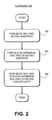
- FIG. 2is a Flowchart representing steps used in a method to form a MEMS structure having an encapsulated MEMS device, in accordance with an embodiment of the present invention.
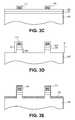
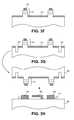
- FIGS. 3A-3Millustrate cross-sectional views representing a series of steps for fabricating a MEMS structure having an encapsulated MEMS device, in accordance with an embodiment of the present invention.
- FIG. 4illustrates a side-on cross-sectional view representing a MEMS structure having an encapsulated MEMS device, wherein a cap substrate is electrically coupled with a device substrate, in accordance with an embodiment of the present invention.
- FIG. 5illustrates a side-on cross-sectional view representing a MEMS structure having an encapsulated MEMS device, wherein a cap substrate includes an inlet, in accordance with an embodiment of the present invention.
- FIG. 6illustrates a top-down view of a wafer with widows cut therein for use in a die singulation approach, in accordance with an embodiment of the present invention.
- An apparatusmay include a first substrate having a silicon-germanium seal ring disposed thereon and a second substrate having a metal seal ring disposed thereon.
- the metal seal ringis aligned with and bonded to the silicon-germanium seal ring to provide a sealed cavity.
- a MEMS devicemay be housed in the sealed cavity.
- the metal seal ringis eutectically bonded to the silicon-germanium seal ring to provide the sealed cavity.
- a methodmay include forming a silicon-germanium seal ring on a first substrate and forming a metal seal ring on a second substrate.
- the metal seal ringis bonded to the silicon-germanium seal ring to form a bond and to provide a sealed cavity that houses a MEMS device.
- the metal seal ringis bonded to the silicon-germanium seal ring to form a eutectic bond between the metal seal ring and the silicon-germanium seal ring.
- Bonding a silicon-germanium seal ring to a metal seal ring to form a sealed cavity for a MEMS devicemay enable the fabrication of a low-contaminant cavity at a relatively low process temperature.
- a first waferis provided which houses a MEMS device inside of the region enclosed by a silicon-germanium seal ring.
- the first waferis bonded to a second wafer having a metal seal ring disposed thereon.
- the first waferis bonded to the second wafer via the silicon-germanium seal ring and the metal seal ring, respectively.
- the metal seal ringmay be composed of gold and may form a eutectic bond with the silicon-germanium seal ring at a process temperature less than 400 degrees Celsius.
- a sealed cavity(the space enclosed inside of the bonded seal rings) may thus be fabricated at a low process temperature.
- the MEMS device on the first waferis housed in a sealed cavity.
- a metal shielding layercan be included on the second wafer, inside of the region enclosed by the metal seal ring. Upon bonding of the first and second wafers, the metal shielding layer is included in the sealed cavity and is provided to mitigate electro-magnetic interference of a device housed in the sealed cavity. Furthermore, in one embodiment, the metal shielding layer can act as a getter layer to facilitate the removal or consumption of impurities that may be trapped in the sealed cavity. Finally, in accordance with an embodiment of the present invention, die singulation, using a set of windows formed in one of the wafers, can be carried out to provide isolated die from the bonded wafers. Such a die singulation approach may minimize the number of masks required for wafer alignment and bonding when isolating a plurality of individual die.
- a MEMS structureincludes an encapsulated MEMS device.
- FIGS. 1A-1Cillustrate cross-sectional views representing a MEMS structure having an encapsulated MEMS device, in accordance with an embodiment of the present invention.
- a MEMS structure 100includes a MEMS device 102 .
- a first (device) substrate 104has a silicon-germanium seal ring 106 disposed thereon.
- a second (cap) substrate 108has a metal seal ring 110 disposed thereon.
- metal seal ring 110is aligned with and bonded to silicon-germanium seal ring 106 and, in a specific embodiment, metal seal ring 110 is eutectically bonded to silicon-germanium seal ring 106 .
- a sealed cavity 112may be provided.
- sealed cavity 112houses MEMS device 102 , as depicted in FIG.
- a metal shielding layer 114is disposed on a surface of cap substrate 108 and is included inside of sealed cavity 112 .
- Contact pads 116are included on device substrate 104 , on the outside of sealed cavity 112 .
- Metal seal ring 110may be included in a metal seal ring stack 113 including a seed layer 118 and a dielectric layer 120 , both of which are depicted in FIG. 1A .
- Sealed cavity 112may seal off exposure of MEMS device 102 to the environment outside of sealed cavity 112 .
- sealed cavityis essentially free of contaminants, such as organic residues or moisture.
- sealed cavity 112is hermetically sealed from the environment outside of sealed cavity 112 .
- the pressure inside of sealed cavity 112is less than the pressure outside of sealed cavity 112 .
- the pressure inside of sealed cavity 112is less than approximately 100 mTorr and the pressure outside of sealed cavity 112 is approximately 1 atmosphere.
- the pressure inside of sealed cavity 112is approximately the same as the pressure outside of sealed cavity 112 .
- sealed cavity 112has a height (taken from the top surface of device substrate 104 to the surface of cap substrate 108 ) approximately in the range of 60-100 microns.
- MEMS device 102is included inside of the region enclosed by silicon-germanium seal ring 106 .
- contact pads 116are included on device substrate 104 , outside of the region enclosed by silicon-germanium seal ring 106 .
- MEMS device 102may be any device that falls within the scope of MEMS technologies.
- MEMS device 102may be any mechanical and electronic structure having a critical dimension of less than approximately 250 microns and fabricated above a substrate using lithography, deposition, and etching processes.
- MEMS device 102is a device such as, but not limited to, a resonator (such as an oscillator), a temperature sensor, a pressure sensor or an inertial sensor (such as an accelerometer or a gyroscope).
- MEMS device 102may have a suspended portion, as depicted in FIG. 1A .
- the suspended portion of MEMS device 102is a suspended feature having a resonant frequency.
- the suspended portionis a feature such as, but not limited to, a beam, a plate, a cantilever arm or a tuning fork.
- MEMS device 102includes a resonating feature 122 flanked by a driver electrode 124 and a sensor electrode 126 , as depicted in FIG. 1B .
- MEMS device 102may be formed from a material suitable to withstand a MEMS fabrication process.
- MEMS device 102is composed of a material such as, but not limited to, a semiconductor, in insulator or a conductor.
- MEMS device 102is composed of a semiconductor material such as, but not limited to, silicon, germanium, silicon-germanium, carbon-doped silicon, carbon-doped silicon-germanium or a III-V material.
- the semiconductor materialmay also be composed of dopant impurity atoms.
- MEMS device 102is composed of polycrystalline silicon-germanium with a germanium atomic concentration approximately in the range of 50-70% and boron dopant impurity atoms with a total atomic concentration approximately in the range of 1 ⁇ 10 18 -5 ⁇ 10 20 atoms/cm 3 .
- MEMS device 102may be composed of a semiconductor material that is formed by a relatively low temperature process.
- MEMS device 102is composed of a semiconductor material formed at a temperature less than approximately 450° C.
- MEMS device 102is composed of an insulating material such as, but not limited to, silicon dioxide, silicon nitride, silicon oxy-nitride or a high-K dielectric material.
- MEMS device 102is composed of a conductor and is formed from a material such as, but not limited to, copper, aluminum, a metal alloy or a metal silicide.
- Silicon-germanium seal ring 106may be composed of any ratio of silicon and germanium suitable for bonding and, in a specific embodiment, suitable for eutectic bonding.
- silicon-germanium seal ring 106is composed of essentially the same material as that of MEMS device 102 .
- silicon-germanium seal ring 106is composed of polycrystalline silicon-germanium with a germanium atomic concentration approximately in the range of 50-70% and boron dopant impurity atoms with a total atomic concentration approximately in the range of 1 ⁇ 10 18 -5 ⁇ 10 20 atoms/cm 3 .
- the width of silicon-germanium seal ring 106may be any width suitable to withstand bonding with metal seal ring 110 .
- the width of silicon-germanium seal ring 106is a width suitable to withstand eutectic bonding with metal seal ring 110 without permitting metal seal ring 110 to flow to the sides of silicon-germanium seal ring 106 during the eutectic bonding process.
- the width of the wall (x) of silicon-germanium seal ring 106is approximately in the range of 50-70 microns.
- the height of silicon-germanium seal ring 106(as measured from the top surface of device substrate 104 ) may be approximately the same as the height of MEMS device 102 .
- the height of silicon-germanium seal ring 106is approximately in the range of 0.5-10 microns.
- more than one MEMS deviceis included inside of the region enclosed by silicon-germanium seal ring 106 .
- Contact pads 116may be composed of any conductive material suitable to withstand a MEMS fabrication process.
- contact pads 116are composed of a material such as, but not limited to, a semiconductor material heavily doped with charge-carrier impurity atoms or a conductor.
- contact pads 116are composed of a heavily doped semiconductor material such as, but not limited to, silicon, germanium, silicon-germanium, carbon-doped silicon or a III-V material.
- contact pads 116are composed of a group IV material heavily doped with charge-carrier impurity atoms such as, but not limited to, boron, indium, phosphorus, arsenic or antimony.
- contact pads 116are composed of polycrystalline silicon-germanium with a germanium atomic concentration approximately in the range of 55-95% and boron dopant impurity atoms with a total atomic concentration approximately in the range of 1 ⁇ 10 20 -5 ⁇ 10 22 atoms/cm 3 .
- contact pads 116are composed of a group III-V material heavily doped with charge-carrier impurity atoms such as, but not limited to, carbon, silicon, germanium, oxygen, sulfur, selenium or tellurium.
- contact pads 116are composed of a conductor and are formed from a material such as, but not limited to, copper, aluminum, a metal alloy or a metal silicide.
- contact pads 116are composed of a material formed at a temperature less than approximately 450° C.
- contact pads 116may be composed of a material having a low resistivity.
- contact pads 116are composed of a material having a volume resistivity less than approximately 1 ⁇ 10 ⁇ 5 ohms ⁇ cm.
- Device substrate 104may be composed of any material suitable to withstand a MEMS fabrication process and to provide structural integrity for a MEMS structure having a suspended member.
- device substrate 104is composed of group IV-based materials such as, but not limited to, crystalline silicon, germanium or silicon-germanium.
- device substrate 104is composed of a III-V material.
- Device substrate 104may also include an insulating layer.
- the insulating layeris composed of a material such as, but not limited to, silicon dioxide, silicon nitride, silicon oxy-nitride or a high-k dielectric layer.
- device substrate 104may be composed essentially of an insulator material.
- device substrate 104is composed essentially of a material such as, but not limited to, glass, quartz or sapphire. Device substrate 104 may further incorporate an integrated circuit.
- device substrate 104includes a plurality of interconnect structures connecting a plurality of micro-electronic devices, both of which are disposed underneath MEMS device 102 .
- the plurality of micro-electronic devicesis a plurality of N-type and P-type transistors and the plurality of interconnect structures is a plurality of metal interconnects that tie the plurality of N-type and P-type transistors into an integrated circuit.
- Device substrate 104may further include conductive electrodes that contact underlying interconnect structures.
- device substrate 104includes a plug or via in contact with contact pads 116 .
- metal shielding layer 114is included inside of the region enclosed by metal seal ring stack 113 .
- Metal shielding layer 114may be composed of a material suitable to protect the performance of a device from electro-magnetic interference.
- metal shielding layeris composed of a material such as, but not limited to, titanium, tungsten, chromium or alloys thereof.
- metal shielding layeralso acts as a getter layer and is provided for removing impurities such as, but not limited to, organic residues or moisture, both of which may be contaminants or by-products in the fabrication and encapsulation of MEMS device 102 .
- Cap substrate 108on which metal shielding layer 114 is disposed, may be composed of any material suitable to support metal seal ring stack 113 and suitable to withstand a subsequent thinning process.
- cap substrate 108is composed of a material such as, but not limited to, silicon, glass, quartz or a III-V compound material.
- Metal seal ring 110may be composed of any material suitable for bonding with silicon-germanium ring 106 .
- metal seal ring 110forms a eutectic bond with silicon-germanium ring 106 and, therefore, the metal-silicon-germanium alloy formed therefrom is a eutectic alloy having a sharp melting point.
- metal seal ring 110is composed of a metal such as, but not limited to, gold, aluminum or alloys thereof.
- the width of metal seal ring 110may be any width suitable to withstand bonding with silicon-germanium ring 106 .
- the width of metal seal ring 110may be a width suitable to withstand eutectic bonding with silicon-germanium ring 106 without flowing from the top to the sides of silicon-germanium seal ring 106 during the eutectic bonding process.
- the width of the wall (y) of metal seal ring 110is smaller than the width of the wall (x) of silicon-germanium seal ring 106 .
- the width of the wall (y) of metal seal ring 110is approximately in the range of 20-40 microns.
- metal seal ring 110is disposed on seed layer 118 and dielectric layer 120 to form metal seal ring stack 113 , as depicted in FIG. 1A .
- the height of metal seal ring stack 113(as measured, e.g., from the surface of cap substrate 108 to the surface of metal seal ring 110 ) may be a height suitable to withstand a subsequent die singulation process and to permit MEMS device 102 to move freely.
- the combined height of metal seal ring stack 113 and silicon-germanium seal ring 106is approximately in the range of 60-100 microns.
- a MEMS deviceis included inside of the region enclosed by metal seal ring 110 .
- metal seal ring 110is disposed directly on cap substrate 108 .
- a MEMS structuremay be fabricated to include an encapsulated MEMS device.
- FIG. 2is a Flowchart 200 representing steps used in a method to form a MEMS structure having an encapsulated MEMS device, in accordance with an embodiment of the present invention.
- FIGS. 3A-3Millustrate cross-sectional views representing a series of steps for fabricating a MEMS structure having an encapsulated MEMS device, in accordance with an embodiment of the present invention.
- a first (metal) seal ringis formed on the top surface of a first (cap) substrate.
- cap substrate 308is provided.
- Cap substrate 308may be composed of a material described in association with cap substrate 108 from FIGS. 1A-1C .
- cap substrate 308has a thickness approximately in the range of 700-800 microns.
- a dielectric layer 301may be disposed on cap substrate 308 to provide a diffusion barrier for a subsequently formed sealed cavity.
- dielectric layer 301is composed of silicon dioxide formed either by chemical vapor deposition or thermal heating of a silicon substrate and has a thickness approximately in the range of 100-500 nanometers.
- a seed layer 303may be disposed on dielectric layer 301 to act as a glue layer during subsequent fabrication of a metal seal ring.
- seed layer 303is composed of a material such as, but not limited to, titanium, chromium, gold, tungsten, nickel or alloys thereof.
- seed layer 303is formed by chemical vapor deposition or physical vapor deposition and has a thickness approximately in the range of 10-200 nanometers.
- metal seal ring 310is formed above cap substrate 308 .
- metal seal ring 310is formed on seed layer 303 , as depicted in FIGS. 3 B and 3 B′.
- Metal seal ring 310may be composed of a material described in association with metal seal ring 110 from FIGS. 1A-1C .
- metal seal ring 310is formed first by blanket deposition by a technique such as, but not limited to, plating, evaporation, sputter deposition or vapor deposition and, subsequently, lithography and etch patterning.
- metal seal ring 310is formed directly, i.e. without the need for subsequent lithographic patterning, by a technique such as, but not limited to, lift-off, selective plating or screen printing.
- metal ring 310is formed to a thickness approximately in the range of 0.5-10 microns.
- the walls of metal seal ring 310may have a width (y) suitable for subsequent bonding to another seal ring.
- the walls of metal seal ring 310have a width (y) suitable for subsequent eutectic bonding to another seal ring without overflowing the surface of that other seal ring.
- the width of metal seal ring 310 as formedis predetermined to allow some room for expansion and/or misalignment during a subsequent eutectic bonding process.
- the as formed width (y) of the walls of metal seal ring 310is approximately in the range of 20-40 microns.
- the region 311 enclosed by metal seal ring 310may be any dimension suitable for encapsulating a MEMS device or a plurality of MEMS devices.
- the height (h) of metal seal ring 310may be extended to include the thicknesses of seed layer 303 , dielectric layer 301 and a recessed portion 305 of cap substrate 302 .
- a mask layer 330is patterned to cover metal seal ring 310 .
- mask layer 330is composed of photo-resist and is patterned by a lithography and etch process.
- seed layer 303 , dielectric layer 301 and cap substrate 302are patterned to form patterned seed layer 318 , patterned dielectric layer 320 , and recessed portion 305 in cap substrate 302 .
- seed layer 303 , dielectric layer 301 and cap substrate 302are patterned by a technique such as, but not limited to, reactive ion etching or wet etching, during which metal ring 310 is protected by mask layer 330 .
- a metal seal ring stack 313may be formed.
- Metal seal ring stack 313may be formed to a height (h) suitable to provide a cavity for a subsequently encapsulated MEMS device and to accommodate a sawing process during die singulation. In one embodiment, the height (h) of metal seal ring stack 313 is greater than approximately 60 microns.
- a metal shielding layermay be formed above cap substrate 302 , inside of the region enclosed by said metal seal ring stack 313 .
- a metal layer 340is deposited above the exposed surface of cap substrate 302 and above mask layer 330 .
- Metal layer 340may be composed of a material described in association with metal shielding layer 114 from FIGS. 1A-1C .
- metal layer 340is formed by a technique such as, but not limited to, sputtering, evaporation or vapor deposition and is formed to a thickness approximately in the range of 50-1000 nanometers. Referring to FIG.
- the portions of metal layer 340 above metal seal ring stack 313are removed to provide a metal shielding layer 314 .
- the portions of metal layer 340 above metal seal ring stack 313are removed by lifting-off mask 330 .
- a wet etch lift-off processis used to remove mask 330 and to provide metal shielding layer 314 .
- a set of trenches 350is formed in the top surface of cap substrate 302 , outside of the region enclosed by metal seal ring stack 313 .
- the set of trenches 350may ultimately be used to provide alignment marks for die singulation.
- the set of trenches 350may have a depth suitable for subsequently forming a set of windows in cap substrate 302 .
- cap substrate 302has a thickness in the range of 700-800 microns and each of the trenches of the set of trenches 350 is formed to a depth approximately in the range of 100-400 microns.
- the width of each of the trenches of the set of trenches 350may be selected to optimize a subsequent alignment process. In one embodiment, the width of each of the trenches of the set of trenches 350 is approximately in the range of 20-100 microns.
- the set of trenches 350is formed by a technique such as, but not limited to, laser cutting, deep reactive ion etching or partial dicing.
- a second (device) substrate 304is provided having a second seal ring 306 disposed thereon.
- a MEMS device 302 and contact pads 316may also be disposed on device substrate 302 , as depicted in FIG. 3H .
- Device substrate 304 , MEMS device 302 and contact pads 316may be composed of a material and may have a function described in association with device substrate 104 , MEMS device 102 and contact pads 116 from FIGS. 1A-1C .
- second seal ring 306is composed of silicon-germanium.
- second seal ring 306is pre-bond aligned with metal seal ring stack 313 on cap substrate 308 , as depicted in FIG. 3H .
- second seal ring 306is bonded to metal seal ring 310 to provide a sealed cavity 312 that houses MEMS device 302 .
- second seal ring 306is bonded to metal seal ring 310 to provide a eutectic bond between the two seal rings.
- metal seal ring 310is composed of gold
- second seal ring 306is composed of silicon-germanium and a eutectic bond is formed between the two seal rings at a temperature less than approximately 400 degrees Celsius.
- metal seal ring 310is composed of gold, second seal ring 306 is composed of silicon-germanium and a eutectic bond is formed between the two seal rings at a temperature of approximately 360 degrees Celsius.
- metal seal ring 310is composed of aluminum, second seal ring 306 is composed of silicon-germanium and a eutectic bond is formed between the two seal rings at a temperature less than approximately 450 degrees Celsius.
- an isopropyl alcohol vapor clean processis carried out on both cap substrate 308 and device substrate 304 immediately prior to bonding.
- cap substrate 308 and device substrate 304are aligned by optical key-to-key alignment.
- second seal ring 306is bonded to a glass seal ring, instead of a metal seal ring, to provide a bond between the two seal rings.
- the bondis a fusion bond and is formed by annealing at a temperature greater than approximately 600 degrees Celsius or at a temperature of approximately 400 degrees Celsius if the annealing is carried out in conjunction with a surface activation process step.
- the bondis an anodic bond and is formed by annealing at a temperature approximately in the range of 200-400 degrees Celsius while the seal rings are grounded with an applied voltage approximately in the range of 500-2000 Volts.
- the bondis a glass frit bond and is formed by using a thin glass layer and annealing at a temperature of approximately 415 degrees Celsius.
- metal seal ring 310is narrower than second seal ring 306 .
- metal seal ring 310has a starting width narrower than the rest of metal seal ring stack 313 , as depicted in FIGS. 3F-3H .
- the width of metal seal ring 310may be initially selected to accommodate expansion during eutectic bonding with second seal ring 306 and to accommodate any misalignment when bonding second seal ring 306 to metal seal ring stack 313 .
- any expansion or misalignmentis accommodated by a wider second seal ring 306 to prevent the migration or flow of metal to a location other than the top surface of second seal ring 306 .
- the use of a wider second seal ringprevents metal contamination of MEMS device 302 .
- the width of metal seal ring 310is initially formed to be narrower than the rest of metal seal ring stack 313 , but following bonding with second seal ring 306 , metal seal ring 310 has a width approximately equal to the width of metal seal ring stack 313 , as depicted in FIGS. 3F-3I . In that embodiment, the final width of metal seal ring 310 remains smaller than the width second seal ring 306 .
- metal seal ring 310is bonded to second seal ring 306 in a reduced pressure atmosphere, i.e. an atmosphere having a pressure less than the pressure of the environment in which a die incorporating MEMS device 302 will be used.
- metal seal ring 310is bonded to second seal ring 306 in an ambient pressure atmosphere, i.e. an atmosphere having a pressure similar to the pressure of the environment in which a die incorporating MEMS device 302 will be used.
- metal seal ring 310is bonded to second seal ring 306 in an increased pressure atmosphere, i.e. an atmosphere having a pressure greater than the pressure of the environment in which a die incorporating MEMS device 302 will be used.
- both cap substrate 308 and device substrate 304are thinned.
- both cap substrate 308 and device substrate 304are thinned to a thickness approximately in the range of 100-200 microns.
- cap substrate 308 and device substrate 304are thinned by grinding the bottom surface of each substrate.
- cap substrate 308is sufficiently thinned to expose the set of trenches 350 , providing a set of windows 360 in cap substrate 308 .
- cap substrate 308is diced along the set of windows 360 , outside of sealed cavity 312 .
- the set of windows 360is used as a set of alignment marks for the dicing of cap substrate 308 .
- the overall bonding processrequires one less mask step for alignment considerations.
- cap substrate 308is diced by sawing.
- device substrate 304is diced outside of the region enclosed by said second seal ring 306 , i.e. outside of sealed cavity 312 .
- a singulated die having a diced cap substrate 308 bonded to a diced device substrate 304is provided to encapsulate MEMS device 302 in sealed cavity 312 .
- a metal layer housed in a sealed cavitymay be used to electrically couple a cap substrate and a device substrate of a MEMS structure.
- FIG. 4illustrates a side-on cross-sectional view representing a MEMS structure having an encapsulated MEMS device, wherein a cap substrate is electrically coupled with a device substrate, in accordance with an embodiment of the present invention.
- a MEMS structure 400includes a MEMS device 402 .
- a first (device) substrate 404has a silicon-germanium seal ring 406 disposed thereon.
- a second (cap) substrate 408has a metal seal ring 410 disposed thereon.
- metal seal ring 410is aligned with and bonded to silicon-germanium seal ring 406 and, in a specific embodiment, metal seal ring 410 is eutectically bonded to silicon-germanium seal ring 406 .
- a sealed cavity 412is provided.
- sealed cavity 412houses MEMS device 402 , as depicted in FIG. 4 .
- Contact pads 416may be included on device substrate 404 , on the outside of sealed cavity 412 .
- Metal seal ring 410may be included in a metal seal ring stack 413 including a seed layer 418 and a dielectric layer 420 , both of which are depicted in FIG. 4 .
- a metal shielding layer 414is disposed on a surface of cap substrate 408 and is included inside of sealed cavity 412 .
- metal shielding layer 414extends along the sidewalls of metal seal ring stack 413 to electrically couple cap substrate 408 with device substrate 404 via metal seal ring 410 .
- the intra-cavity portion 414 A of metal shielding layer 414is electrically coupled to MEMS device 402 via metal seal ring 410 , silicon-germanium seal ring 406 and an interconnect 460 formed in device substrate 404 , as depicted in FIG. 4 .
- a thin film battery 470is housed in sealed cavity 412 on the side of cap substrate 408 .
- thin film battery 470is electrically coupled to MEMS device 402 via portions of metal shielding layer 414 which act as a portion of the terminals for thin film battery 470 .
- Other functionalitymay also be built in to cap substrate 408 .
- the extra-cavity portion 414 B of metal shielding layer 414is electrically coupled to device substrate 404 via metal seal ring 410 and silicon-germanium seal ring 406 .
- a grounding interconnect 480is provided for grounding device substrate 404 , and in a particular embodiment for grounding MEMS device 402 , as depicted in FIG. 4 .
- cap substrate 408includes circuitry disposed on or within its substrate body. The circuitry of cap substrate 408 may be coupled to various circuitry disposed on or within the substrate body of device substrate 404 , including circuitry connected to MEMS device 402 .
- an inletmay be included in a cap substrate to provide access to a MEMS device housed in a cavity formed by the cap substrate.
- FIG. 5illustrates a side-on cross-sectional view representing a MEMS structure having an encapsulated MEMS device, wherein a cap substrate includes an inlet, in accordance with an embodiment of the present invention.
- a MEMS structure 500includes a MEMS device 502 .
- a first (device) substrate 504is bonded to a second (cap) substrate 508 by a seal ring 510 .
- a cavity 512is disposed between device substrate 504 and cap substrate 508 , inside of seal ring 510 .
- MEMS device 502is housed above device substrate 504 and in cavity 512 .
- An inlet 590is disposed in cap substrate 508 , providing an opening to cavity 512 .
- inlet 590includes a V-groove profile having the wider portion closer to MEMS device 502 than the narrower portion, as depicted in FIG. 5 .
- the V-groove profileis formed by etching cap substrate 508 with a hydroxide-based etching solution prior to bonding cap substrate 508 to device substrate 504 .
- seal ring 510is composed of silicon-germanium.
- Inlet 590may be a feature formed in cap substrate 508 that exposes MEMS device 502 to the environment outside of cavity 512 and that permits a waveform 549 to propagate from outside of cavity 512 and into cavity 512 .
- inlet 590is a waveguide.
- inlet 590is disposed in cap substrate 508 to permit a sound wave to enter cavity 512 .
- MEMS device 502is a device such as, but not limited to, a pressure sensor, an acoustic sensor or a light sensor.
- a second inlet 592is disposed in cap substrate 508 and is also provided to permit the sound wave to enter cavity 512 , as depicted in FIG. 5 .
- inlet 590 and second inlet 592are arranged to provide a constructive interference 599 of the sound wave and, thus, are arranged in a grating pattern. Such a constructive interference may amplify the sound wave for improved detection by MEMS device 502 .
- MEMS device 502is included in an array of MEMS devices housed in cavity 512 .
- inlet 590is disposed in cap substrate 508 to permit an optical wave to enter cavity 512 .
- MEMS device 502is a device such as, but not limited to, a pressure sensor, an acoustic sensor or a light sensor.
- MEMS device 502is an optical sensor such as, but not limited to, an infra-red (IR) sensor.
- a second inlet 592is disposed in cap substrate 508 and is also provided to permit the optical wave to enter cavity 512 , as depicted in FIG. 5 .
- inlet 590 and second inlet 592are arranged to provide a constructive interference 599 of the optical wave and, thus, are arranged in a grating pattern. Such a constructive interference may amplify the optical wave for improved detection by MEMS device 502 .
- MEMS device 502is included in an array of MEMS devices housed in cavity 512 .
- a plurality of sealed cavitiesare fabricated from a plurality of metal seal ring and silicon-germanium seal ring pairings disposed on a pair of bonded wafers.
- a sealed cavityis provided for each single MEMS device on a device wafer.
- each sealed cavityhouses a group of MEMS devices.
- FIG. 4illustrates a top-down view of a wafer with widows cut therein for use in a die singulation approach, in accordance with an embodiment of the present invention.
- the backside of a wafer 602has thereon a grid 604 representing locations of individual die for singulation.
- Grid 604is merely provided for illustration purposes and is not necessarily included on the backside of wafer 602 .
- a set of windows 650is formed in wafer 602 .
- the set of windows 650may be formed by a technique and have dimensions similar to those described in association with windows 350 from FIGS. 3G-3J .
- a windowneed not be formed for each die.
- a sufficient number of windowsare provided to enable alignment in a dicing process, but sufficiently few are provided to minimize the impact to the structural integrity of wafer 602 , especially during a wafer thinning process, as described above.
- an apparatusincludes a first substrate having a silicon-germanium seal ring disposed thereon.
- a second substratehas a metal seal ring disposed thereon.
- the metal seal ringis aligned with and bonded to the silicon-germanium seal ring to provide a sealed cavity.
- a MEMS deviceis housed in the sealed cavity.
- the metal seal ringis eutectically bonded to the silicon-germanium seal ring to provide the sealed cavity.
- a methodin accordance with another embodiment of the present invention, includes forming a silicon-germanium seal ring on a first substrate.
- a metal seal ringis formed on a second substrate.
- the metal seal ringis bonded to the silicon-germanium seal ring to provide a sealed cavity that houses a MEMS device.
- the metal seal ringis bonded to the silicon-germanium seal ring to form a eutectic bond between the metal seal ring and the silicon-germanium seal ring.
Landscapes
- Engineering & Computer Science (AREA)
- Microelectronics & Electronic Packaging (AREA)
- Physics & Mathematics (AREA)
- General Physics & Mathematics (AREA)
- Computer Hardware Design (AREA)
- Electromagnetism (AREA)
- Radar, Positioning & Navigation (AREA)
- Remote Sensing (AREA)
- Micromachines (AREA)
Abstract
Description
Claims (24)
Priority Applications (1)
| Application Number | Priority Date | Filing Date | Title |
|---|---|---|---|
| US12/124,043US8349635B1 (en) | 2008-05-20 | 2008-05-20 | Encapsulated MEMS device and method to form the same |
Applications Claiming Priority (1)
| Application Number | Priority Date | Filing Date | Title |
|---|---|---|---|
| US12/124,043US8349635B1 (en) | 2008-05-20 | 2008-05-20 | Encapsulated MEMS device and method to form the same |
Publications (1)
| Publication Number | Publication Date |
|---|---|
| US8349635B1true US8349635B1 (en) | 2013-01-08 |
Family
ID=47427860
Family Applications (1)
| Application Number | Title | Priority Date | Filing Date |
|---|---|---|---|
| US12/124,043Active2029-08-01US8349635B1 (en) | 2008-05-20 | 2008-05-20 | Encapsulated MEMS device and method to form the same |
Country Status (1)
| Country | Link |
|---|---|
| US (1) | US8349635B1 (en) |
Cited By (113)
| Publication number | Priority date | Publication date | Assignee | Title |
|---|---|---|---|---|
| US20130017643A1 (en)* | 2011-07-11 | 2013-01-17 | Siliconware Precision Industries Co., Ltd. | Method for fabricating package structure having mems elements |
| US20130043564A1 (en)* | 2011-08-16 | 2013-02-21 | Lisa H. Karlin | Attaching a mems to a bonding wafer |
| US20130285170A1 (en)* | 2010-09-28 | 2013-10-31 | Taiwan Semiconductor Manufacturing Company, Ltd. | Multiple bonding in wafer level packaging |
| US20140077316A1 (en)* | 2012-04-10 | 2014-03-20 | Sand 9, Inc. | Wafer bonding and related methods and apparatus |
| US20150115376A1 (en)* | 2013-10-24 | 2015-04-30 | Analog Devices, Inc. | MEMS Device with Outgassing Shield |
| US20160023892A1 (en)* | 2014-07-22 | 2016-01-28 | Rf Micro Devices, Inc. | Radio frequency (rf) microelectromechanical systems (mems) devices with gold-doped silicon |
| US20160282609A1 (en)* | 2015-03-26 | 2016-09-29 | Seiko Epson Corporation | Electro-optical device, manufacturing method thereof, and electronic apparatus |
| CN105990129A (en)* | 2015-02-02 | 2016-10-05 | 中芯国际集成电路制造(上海)有限公司 | Semiconductor device and formation method thereof |
| US9630834B2 (en)* | 2014-06-16 | 2017-04-25 | InSense, Inc. | Wafer scale monolithic CMOS-integration of free- and non-free-standing Metal- and Metal alloy-based MEMS structures in a sealed cavity |
| US20170125627A1 (en)* | 2014-09-11 | 2017-05-04 | International Business Machines Corporation | Photodiode structures |
| US20170158489A1 (en)* | 2015-12-08 | 2017-06-08 | Robert Bosch Gmbh | Additional surface for stabilizing the internal cavity pressure over the lifetime |
| US20180069079A1 (en)* | 2016-09-02 | 2018-03-08 | Qualcomm Incorporated | Semiconductor devices including trap rich layer regions |
| US20180086664A1 (en)* | 2016-09-27 | 2018-03-29 | Vaon, Llc | Glass-sensor structures |
| US10005660B1 (en)* | 2017-02-15 | 2018-06-26 | Advanced Semiconductor Engineering, Inc. | Semiconductor package device including microelectromechanical system |
| RU2662061C1 (en)* | 2017-10-25 | 2018-07-23 | Федеральное государственное автономное образовательное учреждение высшего образования "Национальный исследовательский университет "Московский институт электронной техники" | Mems devices sealing method |
| US10081535B2 (en) | 2013-06-25 | 2018-09-25 | Analog Devices, Inc. | Apparatus and method for shielding and biasing in MEMS devices encapsulated by active circuitry |
| WO2018175208A1 (en)* | 2017-03-21 | 2018-09-27 | Invensas Bonding Technologies, Inc. | Seal for microelectronic assembly |
| US10361697B2 (en)* | 2016-12-23 | 2019-07-23 | Skyworks Solutions, Inc. | Switch linearization by compensation of a field-effect transistor |
| CN110164840A (en)* | 2019-05-28 | 2019-08-23 | 罕王微电子(辽宁)有限公司 | A kind of the Direct Bonding device and preparation process of integrated circuit and MEMS |
| US10515925B2 (en) | 2017-04-21 | 2019-12-24 | Invensas Bonding Technologies, Inc. | Die processing |
| US10515913B2 (en) | 2017-03-17 | 2019-12-24 | Invensas Bonding Technologies, Inc. | Multi-metal contact structure |
| US10522499B2 (en) | 2017-02-09 | 2019-12-31 | Invensas Bonding Technologies, Inc. | Bonded structures |
| US10529634B2 (en) | 2017-05-11 | 2020-01-07 | Invensas Bonding Technologies, Inc. | Probe methodology for ultrafine pitch interconnects |
| US10546832B2 (en) | 2016-12-21 | 2020-01-28 | Invensas Bonding Technologies, Inc. | Bonded structures |
| US10607937B2 (en) | 2015-12-18 | 2020-03-31 | Invensas Bonding Technologies, Inc. | Increased contact alignment tolerance for direct bonding |
| US10658313B2 (en) | 2017-12-11 | 2020-05-19 | Invensas Bonding Technologies, Inc. | Selective recess |
| US10727219B2 (en) | 2018-02-15 | 2020-07-28 | Invensas Bonding Technologies, Inc. | Techniques for processing devices |
| US10777533B2 (en) | 2012-08-30 | 2020-09-15 | Invensas Bonding Technologies, Inc. | Heterogeneous device |
| US10784191B2 (en) | 2017-03-31 | 2020-09-22 | Invensas Bonding Technologies, Inc. | Interface structures and methods for forming same |
| US10790262B2 (en) | 2018-04-11 | 2020-09-29 | Invensas Bonding Technologies, Inc. | Low temperature bonded structures |
| US10796936B2 (en) | 2016-12-22 | 2020-10-06 | Invensas Bonding Technologies, Inc. | Die tray with channels |
| US10840205B2 (en) | 2017-09-24 | 2020-11-17 | Invensas Bonding Technologies, Inc. | Chemical mechanical polishing for hybrid bonding |
| US10879226B2 (en) | 2016-05-19 | 2020-12-29 | Invensas Bonding Technologies, Inc. | Stacked dies and methods for forming bonded structures |
| US10879212B2 (en) | 2017-05-11 | 2020-12-29 | Invensas Bonding Technologies, Inc. | Processed stacked dies |
| US10896902B2 (en) | 2016-01-13 | 2021-01-19 | Invensas Bonding Technologies, Inc. | Systems and methods for efficient transfer of semiconductor elements |
| US10923408B2 (en) | 2017-12-22 | 2021-02-16 | Invensas Bonding Technologies, Inc. | Cavity packages |
| US10964664B2 (en) | 2018-04-20 | 2021-03-30 | Invensas Bonding Technologies, Inc. | DBI to Si bonding for simplified handle wafer |
| US10998292B2 (en) | 2018-06-13 | 2021-05-04 | Invensas Bonding Technologies, Inc. | Offset pads over TSV |
| US10998265B2 (en) | 2016-09-30 | 2021-05-04 | Invensas Bonding Technologies, Inc. | Interface structures and methods for forming same |
| US11004757B2 (en) | 2018-05-14 | 2021-05-11 | Invensas Bonding Technologies, Inc. | Bonded structures |
| US11011418B2 (en) | 2005-08-11 | 2021-05-18 | Invensas Bonding Technologies, Inc. | 3D IC method and device |
| US11011494B2 (en) | 2018-08-31 | 2021-05-18 | Invensas Bonding Technologies, Inc. | Layer structures for making direct metal-to-metal bonds at low temperatures in microelectronics |
| US11011503B2 (en) | 2017-12-15 | 2021-05-18 | Invensas Bonding Technologies, Inc. | Direct-bonded optoelectronic interconnect for high-density integrated photonics |
| US11056348B2 (en) | 2018-04-05 | 2021-07-06 | Invensas Bonding Technologies, Inc. | Bonding surfaces for microelectronics |
| US11056390B2 (en) | 2015-06-24 | 2021-07-06 | Invensas Corporation | Structures and methods for reliable packages |
| US11158573B2 (en) | 2018-10-22 | 2021-10-26 | Invensas Bonding Technologies, Inc. | Interconnect structures |
| US11158606B2 (en) | 2018-07-06 | 2021-10-26 | Invensas Bonding Technologies, Inc. | Molded direct bonded and interconnected stack |
| US11169326B2 (en) | 2018-02-26 | 2021-11-09 | Invensas Bonding Technologies, Inc. | Integrated optical waveguides, direct-bonded waveguide interface joints, optical routing and interconnects |
| US11171117B2 (en) | 2018-06-12 | 2021-11-09 | Invensas Bonding Technologies, Inc. | Interlayer connection of stacked microelectronic components |
| US11195748B2 (en) | 2017-09-27 | 2021-12-07 | Invensas Corporation | Interconnect structures and methods for forming same |
| US11205625B2 (en) | 2019-04-12 | 2021-12-21 | Invensas Bonding Technologies, Inc. | Wafer-level bonding of obstructive elements |
| US11203183B2 (en) | 2016-09-27 | 2021-12-21 | Vaon, Llc | Single and multi-layer, flat glass-sensor structures |
| US11205600B2 (en) | 2014-03-12 | 2021-12-21 | Invensas Corporation | Integrated circuits protected by substrates with cavities, and methods of manufacture |
| US11244920B2 (en) | 2018-12-18 | 2022-02-08 | Invensas Bonding Technologies, Inc. | Method and structures for low temperature device bonding |
| US11244916B2 (en) | 2018-04-11 | 2022-02-08 | Invensas Bonding Technologies, Inc. | Low temperature bonded structures |
| US11256004B2 (en) | 2018-03-20 | 2022-02-22 | Invensas Bonding Technologies, Inc. | Direct-bonded lamination for improved image clarity in optical devices |
| US11264345B2 (en) | 2015-08-25 | 2022-03-01 | Invensas Bonding Technologies, Inc. | Conductive barrier direct hybrid bonding |
| US11276676B2 (en) | 2018-05-15 | 2022-03-15 | Invensas Bonding Technologies, Inc. | Stacked devices and methods of fabrication |
| US11296044B2 (en) | 2018-08-29 | 2022-04-05 | Invensas Bonding Technologies, Inc. | Bond enhancement structure in microelectronics for trapping contaminants during direct-bonding processes |
| US11296053B2 (en) | 2019-06-26 | 2022-04-05 | Invensas Bonding Technologies, Inc. | Direct bonded stack structures for increased reliability and improved yield in microelectronics |
| US11348801B2 (en) | 2016-12-28 | 2022-05-31 | Invensas Bonding Technologies, Inc. | Processing stacked substrates |
| US11355404B2 (en) | 2019-04-22 | 2022-06-07 | Invensas Bonding Technologies, Inc. | Mitigating surface damage of probe pads in preparation for direct bonding of a substrate |
| US11367652B2 (en) | 2016-12-28 | 2022-06-21 | Invensas Bonding Technologies, Inc. | Microelectronic assembly from processed substrate |
| US11373963B2 (en) | 2019-04-12 | 2022-06-28 | Invensas Bonding Technologies, Inc. | Protective elements for bonded structures |
| US11380597B2 (en) | 2017-12-22 | 2022-07-05 | Invensas Bonding Technologies, Inc. | Bonded structures |
| US11385278B2 (en) | 2019-05-23 | 2022-07-12 | Invensas Bonding Technologies, Inc. | Security circuitry for bonded structures |
| US11387214B2 (en) | 2017-06-15 | 2022-07-12 | Invensas Llc | Multi-chip modules formed using wafer-level processing of a reconstituted wafer |
| US11393779B2 (en) | 2018-06-13 | 2022-07-19 | Invensas Bonding Technologies, Inc. | Large metal pads over TSV |
| CN114827881A (en)* | 2022-06-29 | 2022-07-29 | 绍兴中芯集成电路制造股份有限公司 | Back cavity forming method, device with back cavity, MEMS microphone and preparation method |
| US11462419B2 (en) | 2018-07-06 | 2022-10-04 | Invensas Bonding Technologies, Inc. | Microelectronic assemblies |
| US11467138B2 (en) | 2016-09-27 | 2022-10-11 | Vaon, Llc | Breathalyzer |
| US11476213B2 (en) | 2019-01-14 | 2022-10-18 | Invensas Bonding Technologies, Inc. | Bonded structures without intervening adhesive |
| US11515291B2 (en) | 2018-08-28 | 2022-11-29 | Adeia Semiconductor Inc. | Integrated voltage regulator and passive components |
| US11538781B2 (en) | 2020-06-30 | 2022-12-27 | Adeia Semiconductor Bonding Technologies Inc. | Integrated device packages including bonded structures |
| US11610846B2 (en) | 2019-04-12 | 2023-03-21 | Adeia Semiconductor Bonding Technologies Inc. | Protective elements for bonded structures including an obstructive element |
| US11621246B2 (en) | 2019-03-29 | 2023-04-04 | Adeia Semiconductor Technologies Llc | Diffused bitline replacement in stacked wafer memory |
| US11626363B2 (en) | 2016-12-29 | 2023-04-11 | Adeia Semiconductor Bonding Technologies Inc. | Bonded structures with integrated passive component |
| US11664357B2 (en) | 2018-07-03 | 2023-05-30 | Adeia Semiconductor Bonding Technologies Inc. | Techniques for joining dissimilar materials in microelectronics |
| US11694925B2 (en) | 2017-10-06 | 2023-07-04 | Adeia Semiconductor Bonding Technologies Inc. | Diffusion barrier collar for interconnects |
| US11710718B2 (en) | 2015-07-10 | 2023-07-25 | Adeia Semiconductor Technologies Llc | Structures and methods for low temperature bonding using nanoparticles |
| US11715730B2 (en) | 2017-03-16 | 2023-08-01 | Adeia Semiconductor Technologies Llc | Direct-bonded LED arrays including optical elements configured to transmit optical signals from LED elements |
| US11721653B2 (en) | 2019-12-23 | 2023-08-08 | Adeia Semiconductor Bonding Technologies Inc. | Circuitry for electrical redundancy in bonded structures |
| US11728273B2 (en) | 2020-09-04 | 2023-08-15 | Adeia Semiconductor Bonding Technologies Inc. | Bonded structure with interconnect structure |
| US11735523B2 (en) | 2020-05-19 | 2023-08-22 | Adeia Semiconductor Bonding Technologies Inc. | Laterally unconfined structure |
| US11742314B2 (en) | 2020-03-31 | 2023-08-29 | Adeia Semiconductor Bonding Technologies Inc. | Reliable hybrid bonded apparatus |
| US11762200B2 (en) | 2019-12-17 | 2023-09-19 | Adeia Semiconductor Bonding Technologies Inc. | Bonded optical devices |
| US11764177B2 (en) | 2020-09-04 | 2023-09-19 | Adeia Semiconductor Bonding Technologies Inc. | Bonded structure with interconnect structure |
| US11760059B2 (en) | 2003-05-19 | 2023-09-19 | Adeia Semiconductor Bonding Technologies Inc. | Method of room temperature covalent bonding |
| US11842894B2 (en) | 2019-12-23 | 2023-12-12 | Adeia Semiconductor Bonding Technologies Inc. | Electrical redundancy for bonded structures |
| US11862602B2 (en) | 2019-11-07 | 2024-01-02 | Adeia Semiconductor Technologies Llc | Scalable architecture for reduced cycles across SOC |
| US11862604B2 (en) | 2018-06-22 | 2024-01-02 | Adeia Semiconductor Inc. | Systems and methods for releveled bump planes for chiplets |
| US11876076B2 (en) | 2019-12-20 | 2024-01-16 | Adeia Semiconductor Technologies Llc | Apparatus for non-volatile random access memory stacks |
| US11881454B2 (en) | 2016-10-07 | 2024-01-23 | Adeia Semiconductor Inc. | Stacked IC structure with orthogonal interconnect layers |
| US11901281B2 (en) | 2019-03-11 | 2024-02-13 | Adeia Semiconductor Bonding Technologies Inc. | Bonded structures with integrated passive component |
| US11908739B2 (en) | 2017-06-05 | 2024-02-20 | Adeia Semiconductor Technologies Llc | Flat metal features for microelectronics applications |
| US11929347B2 (en) | 2020-10-20 | 2024-03-12 | Adeia Semiconductor Technologies Llc | Mixed exposure for large die |
| US11935907B2 (en) | 2014-12-11 | 2024-03-19 | Adeia Semiconductor Technologies Llc | Image sensor device |
| US11973056B2 (en) | 2016-10-27 | 2024-04-30 | Adeia Semiconductor Technologies Llc | Methods for low temperature bonding using nanoparticles |
| US12009338B2 (en) | 2020-03-19 | 2024-06-11 | Adeia Semiconductor Bonding Technologies Inc. | Dimension compensation control for directly bonded structures |
| US12074092B2 (en) | 2018-05-30 | 2024-08-27 | Adeia Semiconductor Inc. | Hard IP blocks with physically bidirectional passageways |
| US12080672B2 (en) | 2019-09-26 | 2024-09-03 | Adeia Semiconductor Bonding Technologies Inc. | Direct gang bonding methods including directly bonding first element to second element to form bonded structure without adhesive |
| US12113054B2 (en) | 2019-10-21 | 2024-10-08 | Adeia Semiconductor Technologies Llc | Non-volatile dynamic random access memory |
| US12142528B2 (en) | 2016-10-07 | 2024-11-12 | Adeia Semiconductor Inc. | 3D chip with shared clock distribution network |
| US12191267B2 (en) | 2019-03-01 | 2025-01-07 | Adeia Semiconductor Technologies, LLC | Nanowire bonding interconnect for fine-pitch microelectronics |
| US12211809B2 (en) | 2020-12-30 | 2025-01-28 | Adeia Semiconductor Bonding Technologies Inc. | Structure with conductive feature and method of forming same |
| US12248869B2 (en) | 2017-08-03 | 2025-03-11 | Adeia Semiconductor Inc. | Three dimensional circuit implementing machine trained network |
| US12272730B2 (en) | 2018-03-29 | 2025-04-08 | Adeia Semiconductor Inc. | Transistor level interconnection methodologies utilizing 3D interconnects |
| US12300634B2 (en) | 2021-08-02 | 2025-05-13 | Adeia Semiconductor Bonding Technologies Inc. | Protective semiconductor elements for bonded structures |
| US12341083B2 (en) | 2023-02-08 | 2025-06-24 | Adeia Semiconductor Bonding Technologies Inc. | Electronic device cooling structures bonded to semiconductor elements |
| US12374641B2 (en) | 2019-06-12 | 2025-07-29 | Adeia Semiconductor Bonding Technologies Inc. | Sealed bonded structures and methods for forming the same |
| US12381128B2 (en) | 2020-12-28 | 2025-08-05 | Adeia Semiconductor Bonding Technologies Inc. | Structures with through-substrate vias and methods for forming the same |
| US12406959B2 (en) | 2018-07-26 | 2025-09-02 | Adeia Semiconductor Bonding Technologies Inc. | Post CMP processing for hybrid bonding |
| US12424584B2 (en) | 2020-10-29 | 2025-09-23 | Adeia Semiconductor Bonding Technologies Inc. | Direct bonding methods and structures |
Citations (40)
| Publication number | Priority date | Publication date | Assignee | Title |
|---|---|---|---|---|
| US4992656A (en)* | 1987-10-26 | 1991-02-12 | Clauser John F | Rotation, acceleration, and gravity sensors using quantum-mechanical matter-wave interferometry with neutral atoms and molecules |
| US5656889A (en) | 1993-07-08 | 1997-08-12 | Futaba Denshi Kogyo Kabushiki Kaisha | Getter, getter device and fluorescent display device |
| US20020017834A1 (en)* | 2000-07-06 | 2002-02-14 | Macdonald Robert I. | Acoustically actuated mems devices |
| US6433401B1 (en)* | 1999-04-06 | 2002-08-13 | Analog Devices Imi, Inc. | Microfabricated structures with trench-isolation using bonded-substrates and cavities |
| US20020130916A1 (en)* | 2001-03-19 | 2002-09-19 | Xerox Corporation | Micro-fabricated shielded conductors |
| US20020179921A1 (en)* | 2001-06-02 | 2002-12-05 | Cohn Michael B. | Compliant hermetic package |
| US20030210453A1 (en)* | 2002-05-09 | 2003-11-13 | Nec Corporation | Optical device and a movable mirror driving method |
| US6658177B1 (en)* | 1999-12-13 | 2003-12-02 | Memlink Ltd. | Switching device and method of fabricating the same |
| US20040029360A1 (en)* | 2001-12-20 | 2004-02-12 | Geefay Frank S. | Wafer-level package with silicon gasket |
| US20040046245A1 (en)* | 2002-09-10 | 2004-03-11 | Minervini Anthony D. | Microelectromechanical system package with environmental and interference shield |
| US20040061618A1 (en)* | 2002-09-30 | 2004-04-01 | Martin Haueis | Sensing of mirror position in an optical switch |
| US20040077121A1 (en)* | 2002-04-22 | 2004-04-22 | Hiroshi Maeda | Solid-state imaging device and method of manufacturing said solid-state imaging device |
| US20040115856A1 (en)* | 2002-11-08 | 2004-06-17 | Jung Kyu-Dong | Method and apparatus for vacuum-mounting a micro electro mechanical system on a substrate |
| US20040150829A1 (en)* | 2001-04-17 | 2004-08-05 | Peter Koch | Interferometric arrangement for determining the transit time of light in a sample |
| US6777267B2 (en)* | 2002-11-01 | 2004-08-17 | Agilent Technologies, Inc. | Die singulation using deep silicon etching |
| US6777263B1 (en)* | 2003-08-21 | 2004-08-17 | Agilent Technologies, Inc. | Film deposition to enhance sealing yield of microcap wafer-level package with vias |
| US20040214380A1 (en)* | 2001-08-24 | 2004-10-28 | Jurgen Leib | Process for producing microelectromechanical components |
| US6822880B2 (en) | 2001-09-28 | 2004-11-23 | Raytheon Company | Multilayer thin film hydrogen getter and internal signal EMI shield for complex three dimensional electronic package components |
| US20050002084A1 (en)* | 2001-05-09 | 2005-01-06 | Wan Chang Feng | Micro-electro-mechanical systems torsional drive |
| US6897551B2 (en) | 2001-07-20 | 2005-05-24 | Saes Getters, S.P.A. | Support for microelectronic, microoptoelectronic or micromechanical devices |
| US20050167795A1 (en)* | 2002-12-27 | 2005-08-04 | Shinko Electric Industries Co., Ltd. | Electronic devices and its production methods |
| US20050168306A1 (en)* | 2000-11-29 | 2005-08-04 | Cohn Michael B. | MEMS device with integral packaging |
| US20050250253A1 (en)* | 2002-10-23 | 2005-11-10 | Cheung Kin P | Processes for hermetically packaging wafer level microscopic structures |
| US20060062420A1 (en)* | 2004-09-16 | 2006-03-23 | Sony Corporation | Microelectromechanical speaker |
| US20060076648A1 (en)* | 2004-09-27 | 2006-04-13 | Brian Gally | System and method for protecting microelectromechanical systems array using structurally reinforced back-plate |
| US20060076634A1 (en)* | 2004-09-27 | 2006-04-13 | Lauren Palmateer | Method and system for packaging MEMS devices with incorporated getter |
| US20060105503A1 (en)* | 2003-07-31 | 2006-05-18 | Xiaoyi Ding | Wafer-level sealed microdevice having trench isolation and methods for making the same |
| US7104129B2 (en) | 2004-02-02 | 2006-09-12 | Invensense Inc. | Vertically integrated MEMS structure with electronics in a hermetically sealed cavity |
| US7166910B2 (en)* | 2000-11-28 | 2007-01-23 | Knowles Electronics Llc | Miniature silicon condenser microphone |
| US20070189558A1 (en)* | 2004-03-09 | 2007-08-16 | Hiroshi Ogura | Electret condenser microphone |
| US7259032B2 (en)* | 2002-11-26 | 2007-08-21 | Murata Manufacturing Co., Ltd. | Hermetically sealing a package to include a barrier metal |
| US20070273728A1 (en)* | 2006-05-24 | 2007-11-29 | Stmicroelectronics, Inc. | Micro-fluidic structure and method of making |
| US20080089536A1 (en)* | 2006-10-11 | 2008-04-17 | Analog Devices, Inc. | Microphone Microchip Device with Differential Mode Noise Suppression |
| US20090041270A1 (en)* | 2004-12-06 | 2009-02-12 | Austriamicrosystems Ag | Mems Microphone And Method For Producing Said Microphone |
| US7560857B2 (en)* | 2006-08-29 | 2009-07-14 | Industrial Technology Research Institute | Package structure of MEMS microphone |
| US7615395B2 (en) | 2003-12-24 | 2009-11-10 | Cavendish Kinetics Limited | Method for containing a device and a corresponding device |
| US7633150B2 (en)* | 2005-07-13 | 2009-12-15 | Shinko Electric Industries Co., Ltd. | Semiconductor device and method for manufacturing semiconductor device |
| US7714274B2 (en)* | 2003-01-14 | 2010-05-11 | Georgia Tech Research Corporation | Integrated micro fuel processor and flow delivery infrastructure |
| US7897503B2 (en)* | 2005-05-12 | 2011-03-01 | The Board Of Trustees Of The University Of Arkansas | Infinitely stackable interconnect device and method |
| US7903831B2 (en)* | 2005-08-20 | 2011-03-08 | Bse Co., Ltd. | Silicon based condenser microphone and packaging method for the same |
- 2008
- 2008-05-20USUS12/124,043patent/US8349635B1/enactiveActive
Patent Citations (40)
| Publication number | Priority date | Publication date | Assignee | Title |
|---|---|---|---|---|
| US4992656A (en)* | 1987-10-26 | 1991-02-12 | Clauser John F | Rotation, acceleration, and gravity sensors using quantum-mechanical matter-wave interferometry with neutral atoms and molecules |
| US5656889A (en) | 1993-07-08 | 1997-08-12 | Futaba Denshi Kogyo Kabushiki Kaisha | Getter, getter device and fluorescent display device |
| US6433401B1 (en)* | 1999-04-06 | 2002-08-13 | Analog Devices Imi, Inc. | Microfabricated structures with trench-isolation using bonded-substrates and cavities |
| US6658177B1 (en)* | 1999-12-13 | 2003-12-02 | Memlink Ltd. | Switching device and method of fabricating the same |
| US20020017834A1 (en)* | 2000-07-06 | 2002-02-14 | Macdonald Robert I. | Acoustically actuated mems devices |
| US7166910B2 (en)* | 2000-11-28 | 2007-01-23 | Knowles Electronics Llc | Miniature silicon condenser microphone |
| US20050168306A1 (en)* | 2000-11-29 | 2005-08-04 | Cohn Michael B. | MEMS device with integral packaging |
| US20020130916A1 (en)* | 2001-03-19 | 2002-09-19 | Xerox Corporation | Micro-fabricated shielded conductors |
| US20040150829A1 (en)* | 2001-04-17 | 2004-08-05 | Peter Koch | Interferometric arrangement for determining the transit time of light in a sample |
| US20050002084A1 (en)* | 2001-05-09 | 2005-01-06 | Wan Chang Feng | Micro-electro-mechanical systems torsional drive |
| US20020179921A1 (en)* | 2001-06-02 | 2002-12-05 | Cohn Michael B. | Compliant hermetic package |
| US6897551B2 (en) | 2001-07-20 | 2005-05-24 | Saes Getters, S.P.A. | Support for microelectronic, microoptoelectronic or micromechanical devices |
| US20040214380A1 (en)* | 2001-08-24 | 2004-10-28 | Jurgen Leib | Process for producing microelectromechanical components |
| US6822880B2 (en) | 2001-09-28 | 2004-11-23 | Raytheon Company | Multilayer thin film hydrogen getter and internal signal EMI shield for complex three dimensional electronic package components |
| US20040029360A1 (en)* | 2001-12-20 | 2004-02-12 | Geefay Frank S. | Wafer-level package with silicon gasket |
| US20040077121A1 (en)* | 2002-04-22 | 2004-04-22 | Hiroshi Maeda | Solid-state imaging device and method of manufacturing said solid-state imaging device |
| US20030210453A1 (en)* | 2002-05-09 | 2003-11-13 | Nec Corporation | Optical device and a movable mirror driving method |
| US20040046245A1 (en)* | 2002-09-10 | 2004-03-11 | Minervini Anthony D. | Microelectromechanical system package with environmental and interference shield |
| US20040061618A1 (en)* | 2002-09-30 | 2004-04-01 | Martin Haueis | Sensing of mirror position in an optical switch |
| US20050250253A1 (en)* | 2002-10-23 | 2005-11-10 | Cheung Kin P | Processes for hermetically packaging wafer level microscopic structures |
| US6777267B2 (en)* | 2002-11-01 | 2004-08-17 | Agilent Technologies, Inc. | Die singulation using deep silicon etching |
| US20040115856A1 (en)* | 2002-11-08 | 2004-06-17 | Jung Kyu-Dong | Method and apparatus for vacuum-mounting a micro electro mechanical system on a substrate |
| US7259032B2 (en)* | 2002-11-26 | 2007-08-21 | Murata Manufacturing Co., Ltd. | Hermetically sealing a package to include a barrier metal |
| US20050167795A1 (en)* | 2002-12-27 | 2005-08-04 | Shinko Electric Industries Co., Ltd. | Electronic devices and its production methods |
| US7714274B2 (en)* | 2003-01-14 | 2010-05-11 | Georgia Tech Research Corporation | Integrated micro fuel processor and flow delivery infrastructure |
| US20060105503A1 (en)* | 2003-07-31 | 2006-05-18 | Xiaoyi Ding | Wafer-level sealed microdevice having trench isolation and methods for making the same |
| US6777263B1 (en)* | 2003-08-21 | 2004-08-17 | Agilent Technologies, Inc. | Film deposition to enhance sealing yield of microcap wafer-level package with vias |
| US7615395B2 (en) | 2003-12-24 | 2009-11-10 | Cavendish Kinetics Limited | Method for containing a device and a corresponding device |
| US7104129B2 (en) | 2004-02-02 | 2006-09-12 | Invensense Inc. | Vertically integrated MEMS structure with electronics in a hermetically sealed cavity |
| US20070189558A1 (en)* | 2004-03-09 | 2007-08-16 | Hiroshi Ogura | Electret condenser microphone |
| US20060062420A1 (en)* | 2004-09-16 | 2006-03-23 | Sony Corporation | Microelectromechanical speaker |
| US20060076634A1 (en)* | 2004-09-27 | 2006-04-13 | Lauren Palmateer | Method and system for packaging MEMS devices with incorporated getter |
| US20060076648A1 (en)* | 2004-09-27 | 2006-04-13 | Brian Gally | System and method for protecting microelectromechanical systems array using structurally reinforced back-plate |
| US20090041270A1 (en)* | 2004-12-06 | 2009-02-12 | Austriamicrosystems Ag | Mems Microphone And Method For Producing Said Microphone |
| US7897503B2 (en)* | 2005-05-12 | 2011-03-01 | The Board Of Trustees Of The University Of Arkansas | Infinitely stackable interconnect device and method |
| US7633150B2 (en)* | 2005-07-13 | 2009-12-15 | Shinko Electric Industries Co., Ltd. | Semiconductor device and method for manufacturing semiconductor device |
| US7903831B2 (en)* | 2005-08-20 | 2011-03-08 | Bse Co., Ltd. | Silicon based condenser microphone and packaging method for the same |
| US20070273728A1 (en)* | 2006-05-24 | 2007-11-29 | Stmicroelectronics, Inc. | Micro-fluidic structure and method of making |
| US7560857B2 (en)* | 2006-08-29 | 2009-07-14 | Industrial Technology Research Institute | Package structure of MEMS microphone |
| US20080089536A1 (en)* | 2006-10-11 | 2008-04-17 | Analog Devices, Inc. | Microphone Microchip Device with Differential Mode Noise Suppression |
Non-Patent Citations (7)
| Title |
|---|
| "Interference and Diffraction", http://web.pdx.edu/~bseipe1/203-CH23.pdf, (date unknown).* |
| "Interference and Diffraction", http://web.pdx.edu/˜bseipe1/203-CH23.pdf, (date unknown).* |
| "This Month in Physics History. May 1801: Thomas Young and the Nature of Light", APS Physics, vol. 17, No. 5, (May 2008).* |
| "Wave Optics, Interference", http://physics.ucsd.edu/students/courses/fall2009/physics1c/documents/5.1Two-slitinterference.pdf, (2009).* |
| CliffsNotes.com. Wave Optics. http://www.cliffsnotes.com/study-guide/topicArticleId-10453,articleId-10442.html, (Jun. 20, 2012).* |
| thefreedictionary.com. Interference. http://encyclopedia2.thefreedictionary.com/p/Interference%20(wave%20motion), (2012).* |
| Wolf, "The Opics of Microscope Image Formation", Methods in Cell Biology, 72, (2003): pp. 11-43.* |
Cited By (235)
| Publication number | Priority date | Publication date | Assignee | Title |
|---|---|---|---|---|
| US11760059B2 (en) | 2003-05-19 | 2023-09-19 | Adeia Semiconductor Bonding Technologies Inc. | Method of room temperature covalent bonding |
| US11515202B2 (en) | 2005-08-11 | 2022-11-29 | Adeia Semiconductor Bonding Technologies Inc. | 3D IC method and device |
| US11011418B2 (en) | 2005-08-11 | 2021-05-18 | Invensas Bonding Technologies, Inc. | 3D IC method and device |
| US11289372B2 (en) | 2005-08-11 | 2022-03-29 | Invensas Bonding Technologies, Inc. | 3D IC method and device |
| US20130285170A1 (en)* | 2010-09-28 | 2013-10-31 | Taiwan Semiconductor Manufacturing Company, Ltd. | Multiple bonding in wafer level packaging |
| US9873610B2 (en)* | 2010-09-28 | 2018-01-23 | Taiwan Semiconductor Manufacturing Company, Ltd. | Multiple bonding in wafer level packaging |
| US8633048B2 (en)* | 2011-07-11 | 2014-01-21 | Siliconware Precision Industries Co., Ltd. | Method for fabricating package structure having MEMS elements |
| US20130017643A1 (en)* | 2011-07-11 | 2013-01-17 | Siliconware Precision Industries Co., Ltd. | Method for fabricating package structure having mems elements |
| US8652865B2 (en)* | 2011-08-16 | 2014-02-18 | Freescale Semiconductor, Inc. | Attaching a MEMS to a bonding wafer |
| US20130043564A1 (en)* | 2011-08-16 | 2013-02-21 | Lisa H. Karlin | Attaching a mems to a bonding wafer |
| US20140077316A1 (en)* | 2012-04-10 | 2014-03-20 | Sand 9, Inc. | Wafer bonding and related methods and apparatus |
| US12199069B2 (en) | 2012-08-30 | 2025-01-14 | Adeia Semiconductor Bonding Technologies Inc. | Heterogeneous annealing method and device |
| US10777533B2 (en) | 2012-08-30 | 2020-09-15 | Invensas Bonding Technologies, Inc. | Heterogeneous device |
| US11631586B2 (en) | 2012-08-30 | 2023-04-18 | Adeia Semiconductor Bonding Technologies Inc. | Heterogeneous annealing method |
| US10081535B2 (en) | 2013-06-25 | 2018-09-25 | Analog Devices, Inc. | Apparatus and method for shielding and biasing in MEMS devices encapsulated by active circuitry |
| US9764946B2 (en)* | 2013-10-24 | 2017-09-19 | Analog Devices, Inc. | MEMs device with outgassing shield |
| US20150115376A1 (en)* | 2013-10-24 | 2015-04-30 | Analog Devices, Inc. | MEMS Device with Outgassing Shield |
| US11205600B2 (en) | 2014-03-12 | 2021-12-21 | Invensas Corporation | Integrated circuits protected by substrates with cavities, and methods of manufacture |
| US9630834B2 (en)* | 2014-06-16 | 2017-04-25 | InSense, Inc. | Wafer scale monolithic CMOS-integration of free- and non-free-standing Metal- and Metal alloy-based MEMS structures in a sealed cavity |
| US9475692B2 (en)* | 2014-07-22 | 2016-10-25 | Qorvo Us, Inc. | Radio frequency (RF) microelectromechanical systems (MEMS) devices with gold-doped silicon |
| US20160023892A1 (en)* | 2014-07-22 | 2016-01-28 | Rf Micro Devices, Inc. | Radio frequency (rf) microelectromechanical systems (mems) devices with gold-doped silicon |
| US10896992B2 (en) | 2014-09-11 | 2021-01-19 | International Business Machines Corporation | Photodiode structures |
| US10050171B2 (en)* | 2014-09-11 | 2018-08-14 | International Business Machines Corporation | Photodiode structures |
| US10141472B2 (en) | 2014-09-11 | 2018-11-27 | International Business Machines Corporation | Photodiode structures |
| US10615302B2 (en) | 2014-09-11 | 2020-04-07 | International Business Machines Corporation | Photodiode structures |
| US10622506B2 (en) | 2014-09-11 | 2020-04-14 | International Business Machines Corporation | Photodiode structures |
| US20170125627A1 (en)* | 2014-09-11 | 2017-05-04 | International Business Machines Corporation | Photodiode structures |
| US10424686B2 (en) | 2014-09-11 | 2019-09-24 | International Business Machines Corporation | Photodiode structures |
| US10453987B2 (en) | 2014-09-11 | 2019-10-22 | International Business Machines Corporation | Photodiode structures |
| US10964840B2 (en) | 2014-09-11 | 2021-03-30 | International Business Machines Corporation | Photodiode structures |
| US12324268B2 (en) | 2014-12-11 | 2025-06-03 | Adeia Semiconductor Technologies Llc | Image sensor device |
| US11935907B2 (en) | 2014-12-11 | 2024-03-19 | Adeia Semiconductor Technologies Llc | Image sensor device |
| CN105990129A (en)* | 2015-02-02 | 2016-10-05 | 中芯国际集成电路制造(上海)有限公司 | Semiconductor device and formation method thereof |
| CN105990129B (en)* | 2015-02-02 | 2019-07-02 | 中芯国际集成电路制造(上海)有限公司 | Semiconductor devices and forming method thereof |
| US10859814B2 (en) | 2015-03-26 | 2020-12-08 | Seiko Epson Corporation | Electro-optical device, manufacturing method thereof, and electronic apparatus |
| CN106019787A (en)* | 2015-03-26 | 2016-10-12 | 精工爱普生株式会社 | Electro-optical device, manufacturing method thereof, and electronic apparatus |
| US20160282609A1 (en)* | 2015-03-26 | 2016-09-29 | Seiko Epson Corporation | Electro-optical device, manufacturing method thereof, and electronic apparatus |
| US11056390B2 (en) | 2015-06-24 | 2021-07-06 | Invensas Corporation | Structures and methods for reliable packages |
| US11710718B2 (en) | 2015-07-10 | 2023-07-25 | Adeia Semiconductor Technologies Llc | Structures and methods for low temperature bonding using nanoparticles |
| US11830838B2 (en) | 2015-08-25 | 2023-11-28 | Adeia Semiconductor Bonding Technologies Inc. | Conductive barrier direct hybrid bonding |
| US12381168B2 (en) | 2015-08-25 | 2025-08-05 | Adeia Semiconductor Bonding Technologies Inc. | Conductive barrier direct hybrid bonding |
| US11264345B2 (en) | 2015-08-25 | 2022-03-01 | Invensas Bonding Technologies, Inc. | Conductive barrier direct hybrid bonding |
| US20170158489A1 (en)* | 2015-12-08 | 2017-06-08 | Robert Bosch Gmbh | Additional surface for stabilizing the internal cavity pressure over the lifetime |
| CN106946218A (en)* | 2015-12-08 | 2017-07-14 | 罗伯特·博世有限公司 | Additional facet for the stable hole internal pressure in service life |
| US10607937B2 (en) | 2015-12-18 | 2020-03-31 | Invensas Bonding Technologies, Inc. | Increased contact alignment tolerance for direct bonding |
| US10896902B2 (en) | 2016-01-13 | 2021-01-19 | Invensas Bonding Technologies, Inc. | Systems and methods for efficient transfer of semiconductor elements |
| US12113056B2 (en) | 2016-05-19 | 2024-10-08 | Adeia Semiconductor Bonding Technologies Inc. | Stacked dies and methods for forming bonded structures |
| US11658173B2 (en) | 2016-05-19 | 2023-05-23 | Adeia Semiconductor Bonding Technologies Inc. | Stacked dies and methods for forming bonded structures |
| US12266650B2 (en) | 2016-05-19 | 2025-04-01 | Adeia Semiconductor Bonding Technologies Inc. | Stacked dies and methods for forming bonded structures |
| US10879226B2 (en) | 2016-05-19 | 2020-12-29 | Invensas Bonding Technologies, Inc. | Stacked dies and methods for forming bonded structures |
| US11837596B2 (en) | 2016-05-19 | 2023-12-05 | Adeia Semiconductor Bonding Technologies Inc. | Stacked dies and methods for forming bonded structures |
| US20180069079A1 (en)* | 2016-09-02 | 2018-03-08 | Qualcomm Incorporated | Semiconductor devices including trap rich layer regions |
| US20180086664A1 (en)* | 2016-09-27 | 2018-03-29 | Vaon, Llc | Glass-sensor structures |
| US11467138B2 (en) | 2016-09-27 | 2022-10-11 | Vaon, Llc | Breathalyzer |
| US11203183B2 (en) | 2016-09-27 | 2021-12-21 | Vaon, Llc | Single and multi-layer, flat glass-sensor structures |
| US10998265B2 (en) | 2016-09-30 | 2021-05-04 | Invensas Bonding Technologies, Inc. | Interface structures and methods for forming same |
| US12218059B2 (en) | 2016-10-07 | 2025-02-04 | Adeia Semiconductor Inc. | Stacked IC structure with orthogonal interconnect layers |
| US12142528B2 (en) | 2016-10-07 | 2024-11-12 | Adeia Semiconductor Inc. | 3D chip with shared clock distribution network |
| US11881454B2 (en) | 2016-10-07 | 2024-01-23 | Adeia Semiconductor Inc. | Stacked IC structure with orthogonal interconnect layers |
| US12027487B2 (en) | 2016-10-27 | 2024-07-02 | Adeia Semiconductor Technologies Llc | Structures for low temperature bonding using nanoparticles |
| US11973056B2 (en) | 2016-10-27 | 2024-04-30 | Adeia Semiconductor Technologies Llc | Methods for low temperature bonding using nanoparticles |
| US12100684B2 (en) | 2016-12-21 | 2024-09-24 | Adeia Semiconductor Bonding Technologies Inc. | Bonded structures |
| US10879207B2 (en) | 2016-12-21 | 2020-12-29 | Invensas Bonding Technologies, Inc. | Bonded structures |
| US11670615B2 (en) | 2016-12-21 | 2023-06-06 | Adeia Semiconductor Bonding Technologies Inc. | Bonded structures |
| US10546832B2 (en) | 2016-12-21 | 2020-01-28 | Invensas Bonding Technologies, Inc. | Bonded structures |
| US10796936B2 (en) | 2016-12-22 | 2020-10-06 | Invensas Bonding Technologies, Inc. | Die tray with channels |
| US10361697B2 (en)* | 2016-12-23 | 2019-07-23 | Skyworks Solutions, Inc. | Switch linearization by compensation of a field-effect transistor |
| US12051621B2 (en) | 2016-12-28 | 2024-07-30 | Adeia Semiconductor Bonding Technologies Inc. | Microelectronic assembly from processed substrate |
| US11348801B2 (en) | 2016-12-28 | 2022-05-31 | Invensas Bonding Technologies, Inc. | Processing stacked substrates |
| US11367652B2 (en) | 2016-12-28 | 2022-06-21 | Invensas Bonding Technologies, Inc. | Microelectronic assembly from processed substrate |
| US12374556B2 (en) | 2016-12-28 | 2025-07-29 | Adeia Semiconductor Bonding Technologies Inc. | Processing stacked substrates |
| US11626363B2 (en) | 2016-12-29 | 2023-04-11 | Adeia Semiconductor Bonding Technologies Inc. | Bonded structures with integrated passive component |
| US12057383B2 (en) | 2016-12-29 | 2024-08-06 | Adeia Semiconductor Bonding Technologies Inc. | Bonded structures with integrated passive component |
| US10522499B2 (en) | 2017-02-09 | 2019-12-31 | Invensas Bonding Technologies, Inc. | Bonded structures |
| US10879210B2 (en) | 2017-02-09 | 2020-12-29 | Invensas Bonding Technologies, Inc. | Bonded structures |
| US10005660B1 (en)* | 2017-02-15 | 2018-06-26 | Advanced Semiconductor Engineering, Inc. | Semiconductor package device including microelectromechanical system |
| US12166024B2 (en) | 2017-03-16 | 2024-12-10 | Adeia Semiconductor Technologies Llc | Direct-bonded LED arrays drivers |
| US12199082B2 (en) | 2017-03-16 | 2025-01-14 | Adeia Semiconductor Technologies Llc | Method of direct-bonded optoelectronic devices |
| US11715730B2 (en) | 2017-03-16 | 2023-08-01 | Adeia Semiconductor Technologies Llc | Direct-bonded LED arrays including optical elements configured to transmit optical signals from LED elements |
| US11088099B2 (en) | 2017-03-17 | 2021-08-10 | Invensas Bonding Technologies, Inc. | Multi-metal contact structure in microelectronic component |
| US10515913B2 (en) | 2017-03-17 | 2019-12-24 | Invensas Bonding Technologies, Inc. | Multi-metal contact structure |
| US11894326B2 (en) | 2017-03-17 | 2024-02-06 | Adeia Semiconductor Bonding Technologies Inc. | Multi-metal contact structure |
| US10508030B2 (en) | 2017-03-21 | 2019-12-17 | Invensas Bonding Technologies, Inc. | Seal for microelectronic assembly |
| US12381119B2 (en) | 2017-03-21 | 2025-08-05 | Adeia Semiconductor Bonding Technologies Inc. | Seal for microelectronic assembly |
| US11257727B2 (en) | 2017-03-21 | 2022-02-22 | Invensas Bonding Technologies, Inc. | Seal for microelectronic assembly |
| US11417576B2 (en) | 2017-03-21 | 2022-08-16 | Invensas Bonding Technologies, Inc. | Seal for microelectronic assembly |
| US12322667B2 (en) | 2017-03-21 | 2025-06-03 | Adeia Semiconductor Bonding Technologies Inc. | Seal for microelectronic assembly |
| WO2018175208A1 (en)* | 2017-03-21 | 2018-09-27 | Invensas Bonding Technologies, Inc. | Seal for microelectronic assembly |
| US10784191B2 (en) | 2017-03-31 | 2020-09-22 | Invensas Bonding Technologies, Inc. | Interface structures and methods for forming same |
| US12431460B2 (en) | 2017-04-21 | 2025-09-30 | Adeia Semiconductor Bonding Technologies Inc. | Die processing |
| US10714449B2 (en) | 2017-04-21 | 2020-07-14 | Invensas Bonding Technologies, Inc. | Die processing |
| US10515925B2 (en) | 2017-04-21 | 2019-12-24 | Invensas Bonding Technologies, Inc. | Die processing |
| US11742315B2 (en) | 2017-04-21 | 2023-08-29 | Adeia Semiconductor Bonding Technologies Inc. | Die processing |
| US10985133B2 (en) | 2017-04-21 | 2021-04-20 | Invensas Bonding Technologies, Inc. | Die processing |
| US12068278B2 (en) | 2017-05-11 | 2024-08-20 | Adeia Semiconductor Bonding Technologies Inc. | Processed stacked dies |
| US10748824B2 (en) | 2017-05-11 | 2020-08-18 | Invensas Bonding Technologies, Inc. | Probe methodology for ultrafine pitch interconnects |
| US10529634B2 (en) | 2017-05-11 | 2020-01-07 | Invensas Bonding Technologies, Inc. | Probe methodology for ultrafine pitch interconnects |
| US11652083B2 (en) | 2017-05-11 | 2023-05-16 | Adeia Semiconductor Bonding Technologies Inc. | Processed stacked dies |
| US10879212B2 (en) | 2017-05-11 | 2020-12-29 | Invensas Bonding Technologies, Inc. | Processed stacked dies |
| US11908739B2 (en) | 2017-06-05 | 2024-02-20 | Adeia Semiconductor Technologies Llc | Flat metal features for microelectronics applications |
| US12374656B2 (en) | 2017-06-15 | 2025-07-29 | Adeia Semiconductor Bonding Technologies Inc. | Multi-chip modules formed using wafer-level processing of a reconstituted wafer |
| US11387214B2 (en) | 2017-06-15 | 2022-07-12 | Invensas Llc | Multi-chip modules formed using wafer-level processing of a reconstituted wafer |
| US12248869B2 (en) | 2017-08-03 | 2025-03-11 | Adeia Semiconductor Inc. | Three dimensional circuit implementing machine trained network |
| US12381173B2 (en) | 2017-09-24 | 2025-08-05 | Adeia Semiconductor Bonding Technologies Inc. | Direct hybrid bonding of substrates having microelectronic components with different profiles and/or pitches at the bonding interface |
| US10840205B2 (en) | 2017-09-24 | 2020-11-17 | Invensas Bonding Technologies, Inc. | Chemical mechanical polishing for hybrid bonding |
| US11552041B2 (en) | 2017-09-24 | 2023-01-10 | Adeia Semiconductor Bonding Technologies Inc. | Chemical mechanical polishing for hybrid bonding |
| US11195748B2 (en) | 2017-09-27 | 2021-12-07 | Invensas Corporation | Interconnect structures and methods for forming same |
| US12322650B2 (en) | 2017-10-06 | 2025-06-03 | Adeia Semiconductor Bonding Technologies Inc. | Diffusion barrier for interconnects |
| US11694925B2 (en) | 2017-10-06 | 2023-07-04 | Adeia Semiconductor Bonding Technologies Inc. | Diffusion barrier collar for interconnects |
| US12198981B2 (en) | 2017-10-06 | 2025-01-14 | Adeia Semiconductor Bonding Technologies Inc. | Diffusion barrier collar for interconnects |
| RU2662061C1 (en)* | 2017-10-25 | 2018-07-23 | Федеральное государственное автономное образовательное учреждение высшего образования "Национальный исследовательский университет "Московский институт электронной техники" | Mems devices sealing method |
| US10658313B2 (en) | 2017-12-11 | 2020-05-19 | Invensas Bonding Technologies, Inc. | Selective recess |
| US11011503B2 (en) | 2017-12-15 | 2021-05-18 | Invensas Bonding Technologies, Inc. | Direct-bonded optoelectronic interconnect for high-density integrated photonics |
| US11600542B2 (en) | 2017-12-22 | 2023-03-07 | Adeia Semiconductor Bonding Technologies Inc. | Cavity packages |
| US11380597B2 (en) | 2017-12-22 | 2022-07-05 | Invensas Bonding Technologies, Inc. | Bonded structures |
| US10923408B2 (en) | 2017-12-22 | 2021-02-16 | Invensas Bonding Technologies, Inc. | Cavity packages |
| US11948847B2 (en) | 2017-12-22 | 2024-04-02 | Adeia Semiconductor Bonding Technologies Inc. | Bonded structures |
| US11037919B2 (en) | 2018-02-15 | 2021-06-15 | Invensas Bonding Technologies, Inc. | Techniques for processing devices |
| US12406975B2 (en) | 2018-02-15 | 2025-09-02 | Adeia Semiconductor Bonding Technologies Inc. | Techniques for processing devices |
| US10727219B2 (en) | 2018-02-15 | 2020-07-28 | Invensas Bonding Technologies, Inc. | Techniques for processing devices |
| US11855064B2 (en) | 2018-02-15 | 2023-12-26 | Adeia Semiconductor Bonding Technologies Inc. | Techniques for processing devices |
| US11860415B2 (en) | 2018-02-26 | 2024-01-02 | Adeia Semiconductor Bonding Technologies Inc. | Integrated optical waveguides, direct-bonded waveguide interface joints, optical routing and interconnects |
| US12271032B2 (en) | 2018-02-26 | 2025-04-08 | Adeia Semiconductor Bonding Technologies Inc. | Integrated optical waveguides, direct-bonded waveguide interface joints, optical routing and interconnects |
| US11169326B2 (en) | 2018-02-26 | 2021-11-09 | Invensas Bonding Technologies, Inc. | Integrated optical waveguides, direct-bonded waveguide interface joints, optical routing and interconnects |
| US12270970B2 (en) | 2018-03-20 | 2025-04-08 | Adeia Semiconductor Bonding Technologies Inc. | Direct-bonded lamination for improved image clarity in optical devices |
| US11256004B2 (en) | 2018-03-20 | 2022-02-22 | Invensas Bonding Technologies, Inc. | Direct-bonded lamination for improved image clarity in optical devices |
| US12272730B2 (en) | 2018-03-29 | 2025-04-08 | Adeia Semiconductor Inc. | Transistor level interconnection methodologies utilizing 3D interconnects |
| US11056348B2 (en) | 2018-04-05 | 2021-07-06 | Invensas Bonding Technologies, Inc. | Bonding surfaces for microelectronics |
| US11804377B2 (en) | 2018-04-05 | 2023-10-31 | Adeia Semiconductor Bonding Technologies, Inc. | Method for preparing a surface for direct-bonding |
| US12341018B2 (en) | 2018-04-05 | 2025-06-24 | Adeia Semiconductor Bonding Technologies Inc. | Method for preparing a surface for direct-bonding |
| US11244916B2 (en) | 2018-04-11 | 2022-02-08 | Invensas Bonding Technologies, Inc. | Low temperature bonded structures |
| US10790262B2 (en) | 2018-04-11 | 2020-09-29 | Invensas Bonding Technologies, Inc. | Low temperature bonded structures |
| US12100676B2 (en) | 2018-04-11 | 2024-09-24 | Adeia Semiconductor Bonding Technologies Inc. | Low temperature bonded structures |
| US12046571B2 (en) | 2018-04-11 | 2024-07-23 | Adeia Semiconductor Bonding Technologies Inc. | Low temperature bonded structures |
| US11515279B2 (en) | 2018-04-11 | 2022-11-29 | Adeia Semiconductor Bonding Technologies Inc. | Low temperature bonded structures |
| US12132020B2 (en) | 2018-04-11 | 2024-10-29 | Adeia Semiconductor Bonding Technologies Inc. | Low temperature bonded structures |
| US10964664B2 (en) | 2018-04-20 | 2021-03-30 | Invensas Bonding Technologies, Inc. | DBI to Si bonding for simplified handle wafer |
| US12300662B2 (en) | 2018-04-20 | 2025-05-13 | Adeia Semiconductor Bonding Technologies Inc. | DBI to SI bonding for simplified handle wafer |
| US11791307B2 (en) | 2018-04-20 | 2023-10-17 | Adeia Semiconductor Bonding Technologies Inc. | DBI to SI bonding for simplified handle wafer |
| US12438122B2 (en) | 2018-04-20 | 2025-10-07 | Adeia Semiconductor Bonding Technologies Inc. | DBI to Si bonding for simplified handle wafer |
| US11004757B2 (en) | 2018-05-14 | 2021-05-11 | Invensas Bonding Technologies, Inc. | Bonded structures |
| US11955393B2 (en) | 2018-05-14 | 2024-04-09 | Adeia Semiconductor Bonding Technologies Inc. | Structures for bonding elements including conductive interface features |
| US12347820B2 (en) | 2018-05-15 | 2025-07-01 | Adeia Semiconductor Bonding Technologies Inc. | Stacked devices and methods of fabrication |
| US11916054B2 (en) | 2018-05-15 | 2024-02-27 | Adeia Semiconductor Bonding Technologies Inc. | Stacked devices and methods of fabrication |
| US11276676B2 (en) | 2018-05-15 | 2022-03-15 | Invensas Bonding Technologies, Inc. | Stacked devices and methods of fabrication |
| US12401011B2 (en) | 2018-05-15 | 2025-08-26 | Adeia Semiconductor Bonding Technologies Inc. | Stacked devices and methods of fabrication |
| US12074092B2 (en) | 2018-05-30 | 2024-08-27 | Adeia Semiconductor Inc. | Hard IP blocks with physically bidirectional passageways |
| US11171117B2 (en) | 2018-06-12 | 2021-11-09 | Invensas Bonding Technologies, Inc. | Interlayer connection of stacked microelectronic components |
| US11393779B2 (en) | 2018-06-13 | 2022-07-19 | Invensas Bonding Technologies, Inc. | Large metal pads over TSV |
| US12243851B2 (en) | 2018-06-13 | 2025-03-04 | Adeia Semiconductor Bonding Technologies Inc. | Offset pads over TSV |
| US12205926B2 (en) | 2018-06-13 | 2025-01-21 | Adeia Semiconductor Bonding Technologies Inc. | TSV as pad |
| US11728313B2 (en) | 2018-06-13 | 2023-08-15 | Adeia Semiconductor Bonding Technologies Inc. | Offset pads over TSV |
| US11749645B2 (en) | 2018-06-13 | 2023-09-05 | Adeia Semiconductor Bonding Technologies Inc. | TSV as pad |
| US10998292B2 (en) | 2018-06-13 | 2021-05-04 | Invensas Bonding Technologies, Inc. | Offset pads over TSV |
| US11955445B2 (en) | 2018-06-13 | 2024-04-09 | Adeia Semiconductor Bonding Technologies Inc. | Metal pads over TSV |
| US11862604B2 (en) | 2018-06-22 | 2024-01-02 | Adeia Semiconductor Inc. | Systems and methods for releveled bump planes for chiplets |
| US11664357B2 (en) | 2018-07-03 | 2023-05-30 | Adeia Semiconductor Bonding Technologies Inc. | Techniques for joining dissimilar materials in microelectronics |
| US11764189B2 (en) | 2018-07-06 | 2023-09-19 | Adeia Semiconductor Bonding Technologies Inc. | Molded direct bonded and interconnected stack |
| US11158606B2 (en) | 2018-07-06 | 2021-10-26 | Invensas Bonding Technologies, Inc. | Molded direct bonded and interconnected stack |
| US12341025B2 (en) | 2018-07-06 | 2025-06-24 | Adeia Semiconductor Bonding Technologies Inc. | Microelectronic assemblies |
| US11462419B2 (en) | 2018-07-06 | 2022-10-04 | Invensas Bonding Technologies, Inc. | Microelectronic assemblies |
| US12266640B2 (en) | 2018-07-06 | 2025-04-01 | Adeia Semiconductor Bonding Technologies Inc. | Molded direct bonded and interconnected stack |
| US11837582B2 (en) | 2018-07-06 | 2023-12-05 | Adeia Semiconductor Bonding Technologies Inc. | Molded direct bonded and interconnected stack |
| US12046482B2 (en) | 2018-07-06 | 2024-07-23 | Adeia Semiconductor Bonding Technologies, Inc. | Microelectronic assemblies |
| US12406959B2 (en) | 2018-07-26 | 2025-09-02 | Adeia Semiconductor Bonding Technologies Inc. | Post CMP processing for hybrid bonding |
| US11515291B2 (en) | 2018-08-28 | 2022-11-29 | Adeia Semiconductor Inc. | Integrated voltage regulator and passive components |
| US12278215B2 (en) | 2018-08-28 | 2025-04-15 | Adeia Semiconductor Inc. | Integrated voltage regulator and passive components |
| US11894345B2 (en) | 2018-08-28 | 2024-02-06 | Adeia Semiconductor Inc. | Integrated voltage regulator and passive components |
| US11967575B2 (en) | 2018-08-29 | 2024-04-23 | Adeia Semiconductor Bonding Technologies Inc. | Bond enhancement structure in microelectronics for trapping contaminants during direct-bonding processes |
| US11296044B2 (en) | 2018-08-29 | 2022-04-05 | Invensas Bonding Technologies, Inc. | Bond enhancement structure in microelectronics for trapping contaminants during direct-bonding processes |
| US12136605B2 (en) | 2018-08-31 | 2024-11-05 | Adeia Semiconductor Bonding Technologies Inc. | Layer structures for making direct metal-to-metal bonds at low temperatures in microelectronics and method for forming the same |
| US11011494B2 (en) | 2018-08-31 | 2021-05-18 | Invensas Bonding Technologies, Inc. | Layer structures for making direct metal-to-metal bonds at low temperatures in microelectronics |
| US11158573B2 (en) | 2018-10-22 | 2021-10-26 | Invensas Bonding Technologies, Inc. | Interconnect structures |
| US12125784B2 (en) | 2018-10-22 | 2024-10-22 | Adeia Semiconductor Bonding Technologies Inc. | Interconnect structures |
| US11756880B2 (en) | 2018-10-22 | 2023-09-12 | Adeia Semiconductor Bonding Technologies Inc. | Interconnect structures |
| US11244920B2 (en) | 2018-12-18 | 2022-02-08 | Invensas Bonding Technologies, Inc. | Method and structures for low temperature device bonding |
| US12154880B2 (en) | 2018-12-18 | 2024-11-26 | Adeia Semiconductor Bonding Technologies Inc. | Method and structures for low temperature device bonding |
| US11817409B2 (en) | 2019-01-14 | 2023-11-14 | Adeia Semiconductor Bonding Technologies Inc. | Directly bonded structures without intervening adhesive and methods for forming the same |
| US11476213B2 (en) | 2019-01-14 | 2022-10-18 | Invensas Bonding Technologies, Inc. | Bonded structures without intervening adhesive |
| US12191267B2 (en) | 2019-03-01 | 2025-01-07 | Adeia Semiconductor Technologies, LLC | Nanowire bonding interconnect for fine-pitch microelectronics |
| US11901281B2 (en) | 2019-03-11 | 2024-02-13 | Adeia Semiconductor Bonding Technologies Inc. | Bonded structures with integrated passive component |
| US12170268B2 (en) | 2019-03-29 | 2024-12-17 | Adeia Semiconductor Technologies Llc | Embedded metal lines |
| US11978724B2 (en) | 2019-03-29 | 2024-05-07 | Adeia Semiconductor Technologies Llc | Diffused bitline replacement in memory |
| US11621246B2 (en) | 2019-03-29 | 2023-04-04 | Adeia Semiconductor Technologies Llc | Diffused bitline replacement in stacked wafer memory |
| US11610846B2 (en) | 2019-04-12 | 2023-03-21 | Adeia Semiconductor Bonding Technologies Inc. | Protective elements for bonded structures including an obstructive element |
| US11728287B2 (en) | 2019-04-12 | 2023-08-15 | Adeia Semiconductor Bonding Technologies Inc. | Wafer-level bonding of obstructive elements |
| US11848284B2 (en) | 2019-04-12 | 2023-12-19 | Adeia Semiconductor Bonding Technologies Inc. | Protective elements for bonded structures |
| US12176303B2 (en) | 2019-04-12 | 2024-12-24 | Adeia Semiconductor Bonding Technologies Inc. | Wafer-level bonding of obstructive elements |
| US11205625B2 (en) | 2019-04-12 | 2021-12-21 | Invensas Bonding Technologies, Inc. | Wafer-level bonding of obstructive elements |
| US11373963B2 (en) | 2019-04-12 | 2022-06-28 | Invensas Bonding Technologies, Inc. | Protective elements for bonded structures |
| US12417950B2 (en) | 2019-04-22 | 2025-09-16 | Adeia Semiconductor Bonding Technologies Inc. | Mitigating surface damage of probe pads in preparation for direct bonding of a substrate |
| US11355404B2 (en) | 2019-04-22 | 2022-06-07 | Invensas Bonding Technologies, Inc. | Mitigating surface damage of probe pads in preparation for direct bonding of a substrate |
| US11978681B2 (en) | 2019-04-22 | 2024-05-07 | Adeia Semiconductor Bonding Technologies Inc. | Mitigating surface damage of probe pads in preparation for direct bonding of a substrate |
| US11385278B2 (en) | 2019-05-23 | 2022-07-12 | Invensas Bonding Technologies, Inc. | Security circuitry for bonded structures |
| US12174246B2 (en) | 2019-05-23 | 2024-12-24 | Adeia Semiconductor Bonding Technologies Inc. | Security circuitry for bonded structures |
| CN110164840A (en)* | 2019-05-28 | 2019-08-23 | 罕王微电子(辽宁)有限公司 | A kind of the Direct Bonding device and preparation process of integrated circuit and MEMS |
| US12374641B2 (en) | 2019-06-12 | 2025-07-29 | Adeia Semiconductor Bonding Technologies Inc. | Sealed bonded structures and methods for forming the same |
| US11955463B2 (en) | 2019-06-26 | 2024-04-09 | Adeia Semiconductor Bonding Technologies Inc. | Direct bonded stack structures for increased reliability and improved yield in microelectronics |
| US11296053B2 (en) | 2019-06-26 | 2022-04-05 | Invensas Bonding Technologies, Inc. | Direct bonded stack structures for increased reliability and improved yield in microelectronics |
| US12272677B2 (en) | 2019-06-26 | 2025-04-08 | Adeia Semiconductor Bonding Technologies Inc. | Direct bonded stack structures for increased reliability and improved yield in microelectronics |
| US12080672B2 (en) | 2019-09-26 | 2024-09-03 | Adeia Semiconductor Bonding Technologies Inc. | Direct gang bonding methods including directly bonding first element to second element to form bonded structure without adhesive |
| US12113054B2 (en) | 2019-10-21 | 2024-10-08 | Adeia Semiconductor Technologies Llc | Non-volatile dynamic random access memory |
| US11862602B2 (en) | 2019-11-07 | 2024-01-02 | Adeia Semiconductor Technologies Llc | Scalable architecture for reduced cycles across SOC |
| US12255176B2 (en) | 2019-11-07 | 2025-03-18 | Adeia Semiconductor Technologies Llc | Scalable architecture for reduced cycles across SOC |
| US12153222B2 (en) | 2019-12-17 | 2024-11-26 | Adeia Semiconductor Bonding Technologies Inc. | Bonded optical devices |
| US11762200B2 (en) | 2019-12-17 | 2023-09-19 | Adeia Semiconductor Bonding Technologies Inc. | Bonded optical devices |
| US12288771B2 (en) | 2019-12-20 | 2025-04-29 | Adeia Semiconductor Technologies Llc | Apparatus for non-volatile random access memory stacks |
| US11876076B2 (en) | 2019-12-20 | 2024-01-16 | Adeia Semiconductor Technologies Llc | Apparatus for non-volatile random access memory stacks |
| US12431449B2 (en) | 2019-12-23 | 2025-09-30 | Adeia Semiconductor Bonding Technologies Inc. | Circuitry for electrical redundancy in bonded structures |
| US11721653B2 (en) | 2019-12-23 | 2023-08-08 | Adeia Semiconductor Bonding Technologies Inc. | Circuitry for electrical redundancy in bonded structures |
| US12308332B2 (en) | 2019-12-23 | 2025-05-20 | Adeia Semiconductor Bonding Technologies Inc. | Circuitry for electrical redundancy in bonded structures |
| US12218107B2 (en) | 2019-12-23 | 2025-02-04 | Adeia Semiconductor Bonding Technologies Inc. | Electrical redundancy for bonded structures |
| US12046583B2 (en) | 2019-12-23 | 2024-07-23 | Adeia Semiconductor Bonding Technologies Inc. | Electrical redundancy for bonded structures |
| US11842894B2 (en) | 2019-12-23 | 2023-12-12 | Adeia Semiconductor Bonding Technologies Inc. | Electrical redundancy for bonded structures |
| US12009338B2 (en) | 2020-03-19 | 2024-06-11 | Adeia Semiconductor Bonding Technologies Inc. | Dimension compensation control for directly bonded structures |
| US12341125B2 (en) | 2020-03-19 | 2025-06-24 | Adeia Semiconductor Bonding Technologies Inc. | Dimension compensation control for directly bonded structures |
| US12300661B2 (en) | 2020-03-31 | 2025-05-13 | Adeia Semiconductor Bonding Technologies Inc. | Reliable hybrid bonded apparatus |
| US11742314B2 (en) | 2020-03-31 | 2023-08-29 | Adeia Semiconductor Bonding Technologies Inc. | Reliable hybrid bonded apparatus |
| US12033943B2 (en) | 2020-05-19 | 2024-07-09 | Adeia Semiconductor Bonding Technologies Inc. | Laterally unconfined structure |
| US11735523B2 (en) | 2020-05-19 | 2023-08-22 | Adeia Semiconductor Bonding Technologies Inc. | Laterally unconfined structure |
| US12046569B2 (en) | 2020-06-30 | 2024-07-23 | Adeia Semiconductor Bonding Technologies Inc. | Integrated device packages with integrated device die and dummy element |
| US11538781B2 (en) | 2020-06-30 | 2022-12-27 | Adeia Semiconductor Bonding Technologies Inc. | Integrated device packages including bonded structures |
| US11631647B2 (en) | 2020-06-30 | 2023-04-18 | Adeia Semiconductor Bonding Technologies Inc. | Integrated device packages with integrated device die and dummy element |
| US12322718B2 (en) | 2020-09-04 | 2025-06-03 | Adeia Semiconductor Bonding Technologies Inc. | Bonded structure with interconnect structure |
| US12176294B2 (en) | 2020-09-04 | 2024-12-24 | Adeia Semiconductor Bonding Technologies, Inc. | Bonded structure with interconnect structure |
| US11728273B2 (en) | 2020-09-04 | 2023-08-15 | Adeia Semiconductor Bonding Technologies Inc. | Bonded structure with interconnect structure |
| US11764177B2 (en) | 2020-09-04 | 2023-09-19 | Adeia Semiconductor Bonding Technologies Inc. | Bonded structure with interconnect structure |
| US11929347B2 (en) | 2020-10-20 | 2024-03-12 | Adeia Semiconductor Technologies Llc | Mixed exposure for large die |
| US12424584B2 (en) | 2020-10-29 | 2025-09-23 | Adeia Semiconductor Bonding Technologies Inc. | Direct bonding methods and structures |
| US12381128B2 (en) | 2020-12-28 | 2025-08-05 | Adeia Semiconductor Bonding Technologies Inc. | Structures with through-substrate vias and methods for forming the same |
| US12211809B2 (en) | 2020-12-30 | 2025-01-28 | Adeia Semiconductor Bonding Technologies Inc. | Structure with conductive feature and method of forming same |
| US12300634B2 (en) | 2021-08-02 | 2025-05-13 | Adeia Semiconductor Bonding Technologies Inc. | Protective semiconductor elements for bonded structures |
| CN114827881A (en)* | 2022-06-29 | 2022-07-29 | 绍兴中芯集成电路制造股份有限公司 | Back cavity forming method, device with back cavity, MEMS microphone and preparation method |
| CN114827881B (en)* | 2022-06-29 | 2023-03-24 | 绍兴中芯集成电路制造股份有限公司 | Back cavity forming method, device with back cavity, MEMS microphone and preparation method |
| US12341083B2 (en) | 2023-02-08 | 2025-06-24 | Adeia Semiconductor Bonding Technologies Inc. | Electronic device cooling structures bonded to semiconductor elements |
Similar Documents
| Publication | Publication Date | Title |
|---|---|---|
| US8349635B1 (en) | Encapsulated MEMS device and method to form the same | |
| US10486964B2 (en) | Method for forming a micro-electro mechanical system (MEMS) including bonding a MEMS substrate to a CMOS substrate via a blocking layer | |
| US10532926B2 (en) | Methods for CMOS-MEMS integrated devices with multiple sealed cavities maintained at various pressures | |
| US8629517B2 (en) | Wafer level packaging | |
| US7767484B2 (en) | Method for sealing and backside releasing of microelectromechanical systems | |
| EP3208231B1 (en) | Method of fabrication of ai/ge bonding in a wafer packaging environment | |
| US7923278B2 (en) | Integrated getter area for wafer level encapsulated microelectromechanical systems | |
| US9567206B2 (en) | Structures and formation methods of micro-electro mechanical system device | |
| US10155655B2 (en) | MEMS devices and fabrication methods thereof | |
| US10160640B2 (en) | Mechanisms for forming micro-electro mechanical system device | |
| US20080290494A1 (en) | Backside release and/or encapsulation of microelectromechanical structures and method of manufacturing same | |
| JP2011505264A (en) | Device with integrated circuit, encapsulated N / MEMS and method of manufacturing the same | |
| US20110221455A1 (en) | Micromechanical component and method for its production | |
| WO2013003784A2 (en) | Process for a sealed mems device with a portion exposed to the environment | |
| JP4539155B2 (en) | Manufacturing method of sensor system | |
| US11097942B2 (en) | Through silicon via (TSV) formation in integrated circuits | |
| US20230294978A1 (en) | Structure for microelectromechanical systems (mems) devices to control pressure at high temperature | |
| CN113364423B (en) | Piezoelectric MEMS resonator, forming method thereof and electronic equipment | |
| US7791183B1 (en) | Universal low cost MEM package | |
| JP2006201158A (en) | Sensor | |
| WO2022246749A1 (en) | Piezoelectric mems resonator and method for forming same, and electrical device | |
| JP2006186358A (en) | Sensor device | |
| JP2006126213A (en) | Sensor system |
Legal Events
| Date | Code | Title | Description |
|---|---|---|---|
| AS | Assignment | Owner name:SILICON CLOCKS, INC., CALIFORNIA Free format text:ASSIGNMENT OF ASSIGNORS INTEREST;ASSIGNORS:GAN, QING;QUEVY, EMMANUEL P.;REEL/FRAME:021093/0097 Effective date:20080519 | |
| AS | Assignment | Owner name:SILICON LABS SC, INC., CALIFORNIA Free format text:CHANGE OF NAME;ASSIGNOR:SILICON CLOCKS, INC.;REEL/FRAME:024369/0134 Effective date:20100423 | |
| AS | Assignment | Owner name:SILICON LABORATORIES INC., TEXAS Free format text:ASSIGNMENT OF ASSIGNORS INTEREST;ASSIGNOR:SILICON LABS SC, INC.;REEL/FRAME:025366/0466 Effective date:20101112 | |
| STCF | Information on status: patent grant | Free format text:PATENTED CASE | |
| FEPP | Fee payment procedure | Free format text:PAYOR NUMBER ASSIGNED (ORIGINAL EVENT CODE: ASPN); ENTITY STATUS OF PATENT OWNER: LARGE ENTITY | |
| FPAY | Fee payment | Year of fee payment:4 | |
| AS | Assignment | Owner name:SEMICONDUCTOR MANUFACTURING INTERNATIONAL (SHANGHA Free format text:ASSIGNMENT OF ASSIGNORS INTEREST;ASSIGNOR:SILICON LABORATORIES INC.;REEL/FRAME:039805/0895 Effective date:20160412 | |
| MAFP | Maintenance fee payment | Free format text:PAYMENT OF MAINTENANCE FEE, 8TH YEAR, LARGE ENTITY (ORIGINAL EVENT CODE: M1552); ENTITY STATUS OF PATENT OWNER: LARGE ENTITY Year of fee payment:8 |