US8349626B2 - Creation of low-relief texture for a photovoltaic cell - Google Patents
Creation of low-relief texture for a photovoltaic cellDownload PDFInfo
- Publication number
- US8349626B2 US8349626B2US12/729,878US72987810AUS8349626B2US 8349626 B2US8349626 B2US 8349626B2US 72987810 AUS72987810 AUS 72987810AUS 8349626 B2US8349626 B2US 8349626B2
- Authority
- US
- United States
- Prior art keywords
- silicon
- photovoltaic cell
- light
- etching
- less
- Prior art date
- Legal status (The legal status is an assumption and is not a legal conclusion. Google has not performed a legal analysis and makes no representation as to the accuracy of the status listed.)
- Expired - Fee Related, expires
Links
- 238000000034methodMethods0.000claimsabstractdescription72
- 229910052710siliconInorganic materials0.000claimsabstractdescription58
- 239000010703siliconSubstances0.000claimsabstractdescription58
- 238000005530etchingMethods0.000claimsabstractdescription43
- XUIMIQQOPSSXEZ-UHFFFAOYSA-NSiliconChemical compound[Si]XUIMIQQOPSSXEZ-UHFFFAOYSA-N0.000claimsdescription57
- 150000002500ionsChemical class0.000claimsdescription9
- 229910021421monocrystalline siliconInorganic materials0.000claimsdescription7
- 229910021419crystalline siliconInorganic materials0.000claims1
- 235000012431wafersNutrition0.000description50
- 239000000463materialSubstances0.000description28
- 229910017052cobaltInorganic materials0.000description16
- 239000010941cobaltSubstances0.000description16
- GUTLYIVDDKVIGB-UHFFFAOYSA-Ncobalt atomChemical compound[Co]GUTLYIVDDKVIGB-UHFFFAOYSA-N0.000description16
- 239000004065semiconductorSubstances0.000description16
- WGTYBPLFGIVFAS-UHFFFAOYSA-Mtetramethylammonium hydroxideChemical compound[OH-].C[N+](C)(C)CWGTYBPLFGIVFAS-UHFFFAOYSA-M0.000description16
- VYPSYNLAJGMNEJ-UHFFFAOYSA-NSilicium dioxideChemical compoundO=[Si]=OVYPSYNLAJGMNEJ-UHFFFAOYSA-N0.000description15
- KFZMGEQAYNKOFK-UHFFFAOYSA-NIsopropanolChemical compoundCC(C)OKFZMGEQAYNKOFK-UHFFFAOYSA-N0.000description12
- 239000002019doping agentSubstances0.000description11
- 238000004519manufacturing processMethods0.000description11
- 230000004888barrier functionEffects0.000description8
- RTAQQCXQSZGOHL-UHFFFAOYSA-NTitaniumChemical compound[Ti]RTAQQCXQSZGOHL-UHFFFAOYSA-N0.000description7
- 229910052814silicon oxideInorganic materials0.000description7
- 239000010936titaniumSubstances0.000description7
- 229910052719titaniumInorganic materials0.000description7
- KWYUFKZDYYNOTN-UHFFFAOYSA-MPotassium hydroxideChemical compound[OH-].[K+]KWYUFKZDYYNOTN-UHFFFAOYSA-M0.000description6
- HEMHJVSKTPXQMS-UHFFFAOYSA-MSodium hydroxideChemical compound[OH-].[Na+]HEMHJVSKTPXQMS-UHFFFAOYSA-M0.000description6
- 229910045601alloyInorganic materials0.000description6
- 239000000956alloySubstances0.000description6
- 229910021417amorphous siliconInorganic materials0.000description6
- 238000004299exfoliationMethods0.000description6
- KRHYYFGTRYWZRS-UHFFFAOYSA-NFluoraneChemical compoundFKRHYYFGTRYWZRS-UHFFFAOYSA-N0.000description5
- 239000004642PolyimideSubstances0.000description5
- 229920001721polyimidePolymers0.000description5
- 238000004140cleaningMethods0.000description4
- 239000007943implantSubstances0.000description4
- 239000000377silicon dioxideSubstances0.000description4
- 235000012239silicon dioxideNutrition0.000description4
- UFHFLCQGNIYNRP-UHFFFAOYSA-NHydrogenChemical compound[H][H]UFHFLCQGNIYNRP-UHFFFAOYSA-N0.000description3
- 239000001257hydrogenSubstances0.000description3
- 229910052739hydrogenInorganic materials0.000description3
- 229910021424microcrystalline siliconInorganic materials0.000description3
- QPJSUIGXIBEQAC-UHFFFAOYSA-Nn-(2,4-dichloro-5-propan-2-yloxyphenyl)acetamideChemical compoundCC(C)OC1=CC(NC(C)=O)=C(Cl)C=C1ClQPJSUIGXIBEQAC-UHFFFAOYSA-N0.000description3
- 229910021420polycrystalline siliconInorganic materials0.000description3
- 229910021332silicideInorganic materials0.000description3
- FVBUAEGBCNSCDD-UHFFFAOYSA-Nsilicide(4-)Chemical compound[Si-4]FVBUAEGBCNSCDD-UHFFFAOYSA-N0.000description3
- 239000000758substrateSubstances0.000description3
- 239000004094surface-active agentSubstances0.000description3
- XOJVVFBFDXDTEG-UHFFFAOYSA-NNorphytaneNatural productsCC(C)CCCC(C)CCCC(C)CCCC(C)CXOJVVFBFDXDTEG-UHFFFAOYSA-N0.000description2
- 229910052581Si3N4Inorganic materials0.000description2
- XLOMVQKBTHCTTD-UHFFFAOYSA-NZinc monoxideChemical compound[Zn]=OXLOMVQKBTHCTTD-UHFFFAOYSA-N0.000description2
- 238000000137annealingMethods0.000description2
- 230000003667anti-reflective effectEffects0.000description2
- 239000012298atmosphereSubstances0.000description2
- 239000003795chemical substances by applicationSubstances0.000description2
- 230000005684electric fieldEffects0.000description2
- 229910052734heliumInorganic materials0.000description2
- 239000001307heliumSubstances0.000description2
- 239000004816latexSubstances0.000description2
- 229920000126latexPolymers0.000description2
- 239000007788liquidSubstances0.000description2
- 229910052751metalInorganic materials0.000description2
- 239000002184metalSubstances0.000description2
- HQVNEWCFYHHQES-UHFFFAOYSA-Nsilicon nitrideChemical compoundN12[Si]34N5[Si]62N3[Si]51N64HQVNEWCFYHHQES-UHFFFAOYSA-N0.000description2
- 238000004544sputter depositionMethods0.000description2
- 238000002207thermal evaporationMethods0.000description2
- 229910052721tungstenInorganic materials0.000description2
- 229910001218Gallium arsenideInorganic materials0.000description1
- OAICVXFJPJFONN-UHFFFAOYSA-NPhosphorusChemical compound[P]OAICVXFJPJFONN-UHFFFAOYSA-N0.000description1
- 229910000577Silicon-germaniumInorganic materials0.000description1
- BQCADISMDOOEFD-UHFFFAOYSA-NSilverChemical compound[Ag]BQCADISMDOOEFD-UHFFFAOYSA-N0.000description1
- 229910004166TaNInorganic materials0.000description1
- 229910004200TaSiNInorganic materials0.000description1
- 229910001069Ti alloyInorganic materials0.000description1
- 229910008599TiWInorganic materials0.000description1
- ATJFFYVFTNAWJD-UHFFFAOYSA-NTinChemical compound[Sn]ATJFFYVFTNAWJD-UHFFFAOYSA-N0.000description1
- GWEVSGVZZGPLCZ-UHFFFAOYSA-NTitan oxideChemical compoundO=[Ti]=OGWEVSGVZZGPLCZ-UHFFFAOYSA-N0.000description1
- LEVVHYCKPQWKOP-UHFFFAOYSA-N[Si].[Ge]Chemical compound[Si].[Ge]LEVVHYCKPQWKOP-UHFFFAOYSA-N0.000description1
- 229910052785arsenicInorganic materials0.000description1
- RQNWIZPPADIBDY-UHFFFAOYSA-Narsenic atomChemical compound[As]RQNWIZPPADIBDY-UHFFFAOYSA-N0.000description1
- 230000000712assemblyEffects0.000description1
- 238000000429assemblyMethods0.000description1
- 230000003190augmentative effectEffects0.000description1
- 239000000969carrierSubstances0.000description1
- 238000006243chemical reactionMethods0.000description1
- 150000001875compoundsChemical class0.000description1
- 239000004020conductorSubstances0.000description1
- 238000007796conventional methodMethods0.000description1
- 238000001816coolingMethods0.000description1
- 239000013078crystalSubstances0.000description1
- 238000005520cutting processMethods0.000description1
- 230000007423decreaseEffects0.000description1
- 239000003989dielectric materialSubstances0.000description1
- 238000009792diffusion processMethods0.000description1
- 239000012530fluidSubstances0.000description1
- 238000009472formulationMethods0.000description1
- 239000007789gasSubstances0.000description1
- 229910052732germaniumInorganic materials0.000description1
- GNPVGFCGXDBREM-UHFFFAOYSA-Ngermanium atomChemical compound[Ge]GNPVGFCGXDBREM-UHFFFAOYSA-N0.000description1
- 239000011521glassSubstances0.000description1
- SWQJXJOGLNCZEY-UHFFFAOYSA-Nhelium atomChemical compound[He]SWQJXJOGLNCZEY-UHFFFAOYSA-N0.000description1
- -1helium ionsChemical class0.000description1
- 239000012535impuritySubstances0.000description1
- AMGQUBHHOARCQH-UHFFFAOYSA-Nindium;oxotinChemical compound[In].[Sn]=OAMGQUBHHOARCQH-UHFFFAOYSA-N0.000description1
- 230000000977initiatory effectEffects0.000description1
- 238000005468ion implantationMethods0.000description1
- 238000010884ion-beam techniqueMethods0.000description1
- 239000011159matrix materialSubstances0.000description1
- 239000013081microcrystalSubstances0.000description1
- 239000000203mixtureSubstances0.000description1
- 229910052750molybdenumInorganic materials0.000description1
- 229910021423nanocrystalline siliconInorganic materials0.000description1
- 229910052759nickelInorganic materials0.000description1
- 150000004767nitridesChemical class0.000description1
- 230000006911nucleationEffects0.000description1
- 238000010899nucleationMethods0.000description1
- 229910052698phosphorusInorganic materials0.000description1
- 239000011574phosphorusSubstances0.000description1
- 229920003223poly(pyromellitimide-1,4-diphenyl ether)Polymers0.000description1
- 238000002310reflectometryMethods0.000description1
- 238000001878scanning electron micrographMethods0.000description1
- 238000007650screen-printingMethods0.000description1
- 229910052709silverInorganic materials0.000description1
- 239000004332silverSubstances0.000description1
- 239000000126substanceSubstances0.000description1
- 229910052715tantalumInorganic materials0.000description1
- 229910052718tinInorganic materials0.000description1
- XOLBLPGZBRYERU-UHFFFAOYSA-Ntin dioxideChemical compoundO=[Sn]=OXOLBLPGZBRYERU-UHFFFAOYSA-N0.000description1
- 229910001887tin oxideInorganic materials0.000description1
- OGIDPMRJRNCKJF-UHFFFAOYSA-Ntitanium oxideInorganic materials[Ti]=OOGIDPMRJRNCKJF-UHFFFAOYSA-N0.000description1
- 239000012780transparent materialSubstances0.000description1
- WFKWXMTUELFFGS-UHFFFAOYSA-NtungstenChemical compound[W]WFKWXMTUELFFGS-UHFFFAOYSA-N0.000description1
- 239000010937tungstenSubstances0.000description1
- 238000009827uniform distributionMethods0.000description1
- 239000011787zinc oxideSubstances0.000description1
- 229910052726zirconiumInorganic materials0.000description1
Images


Classifications
- H—ELECTRICITY
- H10—SEMICONDUCTOR DEVICES; ELECTRIC SOLID-STATE DEVICES NOT OTHERWISE PROVIDED FOR
- H10F—INORGANIC SEMICONDUCTOR DEVICES SENSITIVE TO INFRARED RADIATION, LIGHT, ELECTROMAGNETIC RADIATION OF SHORTER WAVELENGTH OR CORPUSCULAR RADIATION
- H10F77/00—Constructional details of devices covered by this subclass
- H10F77/70—Surface textures, e.g. pyramid structures
- H10F77/703—Surface textures, e.g. pyramid structures of the semiconductor bodies, e.g. textured active layers
- H—ELECTRICITY
- H10—SEMICONDUCTOR DEVICES; ELECTRIC SOLID-STATE DEVICES NOT OTHERWISE PROVIDED FOR
- H10F—INORGANIC SEMICONDUCTOR DEVICES SENSITIVE TO INFRARED RADIATION, LIGHT, ELECTROMAGNETIC RADIATION OF SHORTER WAVELENGTH OR CORPUSCULAR RADIATION
- H10F71/00—Manufacture or treatment of devices covered by this subclass
- H10F71/139—Manufacture or treatment of devices covered by this subclass using temporary substrates
- Y—GENERAL TAGGING OF NEW TECHNOLOGICAL DEVELOPMENTS; GENERAL TAGGING OF CROSS-SECTIONAL TECHNOLOGIES SPANNING OVER SEVERAL SECTIONS OF THE IPC; TECHNICAL SUBJECTS COVERED BY FORMER USPC CROSS-REFERENCE ART COLLECTIONS [XRACs] AND DIGESTS
- Y02—TECHNOLOGIES OR APPLICATIONS FOR MITIGATION OR ADAPTATION AGAINST CLIMATE CHANGE
- Y02E—REDUCTION OF GREENHOUSE GAS [GHG] EMISSIONS, RELATED TO ENERGY GENERATION, TRANSMISSION OR DISTRIBUTION
- Y02E10/00—Energy generation through renewable energy sources
- Y02E10/50—Photovoltaic [PV] energy
Definitions
- the inventionrelates to methods of making low-relief texture at the surface of a thin lamina for use in a photovoltaic cell.
- the light-facing surface of a photovoltaic cellis perfectly planar, a high proportion of incident light may be reflected from the surface rather than entering the cell to be absorbed and converted to electric current.
- a planar reflective back surfacewill also tend to reflect light back out of the cell. Texturing the light-facing surface, the back surface, or both surfaces of a photovoltaic cell such that they are not perfectly planar will tend to refract or reflect incident light in a way that will generally improve conversion efficiency of the cell.
- the present inventionis defined by the following claims, and nothing in this section should be taken as a limitation on those claims.
- the inventionis directed to low-relief texture for use in a photovoltaic cell and methods of making such texture.
- a first aspect of the inventionprovides for a method to texture a surface of a photovoltaic cell, the method comprising: buffing a first surface of a silicon body; etching the buffed first surface; and fabricating the photovoltaic cell, wherein the first surface is a light-facing surface in the photovoltaic cell, wherein, after the etching step, at least fifty percent of the first surface has a peak-to-valley height less than about one micron and an average peak-to-peak distance of less than about one micron, and wherein, in the completed photovoltaic cell, average reflectance for light having wavelength between 375 and 1010 nm at the light-facing surface is no more than about five percent.
- Another aspect of the inventionprovides for a method to texture a surface of a photovoltaic cell, the method comprising: implanting ions in a silicon body to define a cleave plane; cleaving a silicon lamina from the silicon body at the cleave plane, creating a cleaved surface; buffing the cleaved surface; etching the buffed cleaved surface; and fabricating the photovoltaic cell, wherein the cleaved surface is a light-facing surface in the photovoltaic cell, wherein, after the etching step, at least fifty percent of the light-facing surface has a peak-to-valley height less than about one micron and an average peak-to-peak distance of less than about one micron, and wherein, in the completed photovoltaic cell, average reflectance for light having wavelength between 375 and 1010 nm at the light-facing surface is no more than about five percent.
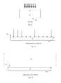
- FIG. 1is a cross-sectional view of a prior art photovoltaic cell.
- FIGS. 2 a - 2 dare cross-sectional views of stages of fabrication of a photovoltaic cell formed according to an embodiment of U.S. patent application Ser. No. 12/026,530.
- FIGS. 3 a and 3 bare cross-sectional views illustrating texturing the front or back surface of a prior art photovoltaic cell to increase the travel length of light within the cell.
- FIGS. 4 a - 4 care cross-sectional views illustrating conventional creation of surface texture for a prior art photovoltaic cell.
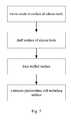
- FIG. 5is a flow chart summarizing steps in a method to create a textured surface according to an embodiment of the present invention.
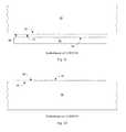
- FIGS. 6 a - 6 eare cross-sectional views illustration fabrication of a photovoltaic cell textured according to an embodiment of the present invention.
- FIG. 7is a flow chart summarizing steps in a method to create a textured surface according to another embodiment of the present invention.
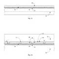
- FIG. 8is a cross-sectional view illustrating fabrication of a photovoltaic cell textured according to another embodiment of the present invention.
- a conventional prior art photovoltaic cellincludes a p ⁇ n diode; an example is shown in FIG. 1 .
- a depletion zoneforms at the p ⁇ n junction, creating an electric field.
- Incident photonsincident light is indicated by arrows
- electronstend to migrate toward the n region of the diode, while holes migrate toward the p region, resulting in current, called photocurrent.
- the dopant concentration of one regionwill be higher than that of the other, so the junction is either a p+/n ⁇ junction (as shown in FIG. 1 ) or a n+/p ⁇ junction.
- the more lightly doped regionis known as the base of the photovoltaic cell, while the more heavily doped region, of opposite conductivity type, is known as the emitter. Most carriers are generated within the base, and it is typically the thickest portion of the cell. The base and emitter together form the active region of the cell.
- the cellalso frequently includes a heavily doped contact region in electrical contact with the base, and of the same conductivity type, to improve current flow. In the example shown in FIG. 1 , the heavily doped contact region is n-type.
- Sivaram et al.U.S. patent application Ser. No. 12/026,530, “Method to Form a Photovoltaic Cell Comprising a Thin Lamina,” filed Feb. 5, 2008, owned by the assignee of the present invention and hereby incorporated by reference, describes fabrication of a photovoltaic cell comprising a thin semiconductor lamina formed of non-deposited semiconductor material.
- a semiconductor donor wafer 20is implanted through first surface 10 with one or more species of gas ions, for example hydrogen and/or helium ions.
- the implanted ionsdefine a cleave plane 30 within the semiconductor donor wafer.
- gas ionsfor example hydrogen and/or helium ions
- donor wafer 20is affixed at first surface 10 to receiver 60 .
- an annealcauses lamina 40 to cleave from donor wafer 20 at cleave plane 30 , creating second surface 62 .
- additional processing before and after the cleaving stepforms a photovoltaic cell comprising semiconductor lamina 40 , which is between about 0.2 and about 100 microns thick, for example between about 0.2 and about 50 microns, for example between about 1 and about 20 microns thick, in some embodiments between about 1 and about 10 microns thick, though any thickness within the named range is possible.
- Receiver 60may be a discrete receiver element having a maximum width no more than 50 percent greater than that of donor wafer 10 , and preferably about the same width, as described in Herner, U.S. patent application Ser. No. 12/057,265, “Method to Form a Photovoltaic Cell Comprising a Thin Lamina Bonded to a Discrete Receiver Element,” filed on Mar. 27, 2008, owned by the assignee of the present application and hereby incorporated by reference.
- a plurality of donor wafersmay be affixed to a single, larger receiver, and a lamina cleaved from each donor wafer.
- photovoltaic cellsrather than being formed from sliced wafers, are formed of thin semiconductor laminae without wasting silicon through kerf loss or by fabrication of an unnecessarily thick cell, thus reducing cost.
- the same donor wafercan be reused to form multiple laminae, further reducing cost, and may be resold after exfoliation of multiple laminae for some other use.
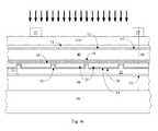
- FIG. 3 ait is well known to texture a light-facing surface 114 of a photovoltaic cell, reducing reflection and causing incident light to be refracted into the cell, as shown. Light may enter the cell, but may pass all the way through the cell without creating any electron-hole pairs, failing to generate any photocurrent and reducing the efficiency of the cell. To avoid allowing light to escape, typically the back surface of the cell is reflective, so that light that passes through the cell is reflected back into the cell from the back surface. Back surface 112 may be textured, as in FIG.
- etchingIn photovoltaic cells formed from monocrystalline wafers, it is conventional to create surface texture by etching the wafers with a crystallographically selective etchant.
- Selective etchantsincluding KOH, NaOH, and tetramethylammonium hydroxide (TMAH), for example, etch the (100) and (110) crystallographic planes of silicon at a higher rate than the (111) plane.
- TMAHtetramethylammonium hydroxide
- TMAHtetramethylammonium hydroxide
- pyramidsgradually begin to form. After sufficient time, the pyramids meet, and the etch rate slows. About 30 minutes or more of etching at the surface of a standard (100)-oriented wafer produces the regular pyramids of FIG. 4 c , which will typically have a peak-to-valley height on the order of a few microns to tens of microns. Such a surface, as described earlier, decreases reflection from the light-facing surface and increases travel length within the body of the photovoltaic cell.
- a methodis described to create surface texture for use in a photovoltaic cell.
- the surface texture of the present inventioncan be achieved with much shorter etching time, with much less silicon loss, than the conventional process.
- the resulting surfacehas low reflectance, and in general the relief produced is small, having an average peak-to-valley height of less than about 1 micron, generally less than about 0.8 microns, for example 0.5 microns or less. Peak-to-peak distance is small as well, less than about 1 micron, generally less than about 0.8 microns, for example 0.5 microns or less.
- This novel methodcan be performed either to texture a surface of a conventional silicon wafer having a thickness of 100 microns, 200 microns, or more; or to texture a surface of a thin lamina cleaved from a thicker body such as a silicon wafer, the lamina having a thickness between about 0.5 and about 20 microns, for example between about 0.5 and about 10 microns, as described by Sivaram et al., earlier incorporated.
- the sub-micron relief created by this methodis particularly well-suited to the thin lamina produced by the method of Sivaram.
- the method of the present inventionprovides the advantage of reduced etch time.
- a surface of a silicon bodyis first cleaned in a conventional cleaning step, for example by a hydrofluoric acid (HF) dip.
- a silicon oxide layeris grown on the silicon surface. This oxide can be allowed to grow simply by exposing the surface to atmosphere at room temperature, or can be chemically or thermally grown.
- the oxideshould be very thin, for example 100 angstroms or less, in most instances 50 angstroms or less. As will be understood, some silicon is consumed at the silicon surface to form the silicon oxide layer. In some embodiments, creation of the silicon oxide layer may be omitted.
- a buffing stepis performed at the silicon surface. This buffing step is performed with very little pressure applied, for example 0.5 psi or less. Buffing is performed with a lightly textured material. The powder-free latex used in a standard textured cleanroom glove is an appropriate buffing agent. Buffing is very brief, preferably with only one or two light passes performed over the silicon surface.
- a crystallographically selective etchantsuch as KOH or TMAH.
- a surfactantsuch as isopropyl alcohol (IPA) is included.
- IPAisopropyl alcohol
- the etchis allowed to proceed, then stopped after a predetermined period of time, which will vary with the etchant formulation and etch conditions, as will be described in greater detail later. In most embodiments, etching will take place for about twelve minutes or less. Very little silicon is lost during this etch. By weight, silicon loss per unit area is generally a total of about 0.3 mg/cm 2 or less at a textured surface.
- Etching at the buffed silicon surfacecreates low-relief texture.
- At least 50 percent, and generally at least 95 percent, of first surface 15has peak-to-valley height less than about one micron, for example less than about 0.8 micron, in some instances less than about 0.5 microns; and has average peak-to-peak distance less than about one micron, for example less than about 0.8 micron, in some instances less than about 0.5 micron.
- a photovoltaic cellis fabricated (specific fabrication examples will be provided) in which the textured surface is a light-facing surface, or, in some embodiments, a back surface. In the finished device, average reflectance for light having wavelength between 375 and 1010 nm at a light-facing surface is low, about 6 percent or less, for example about 5 percent or less. In some embodiments, reflectance is about 3.5 percent or less.
- buffingmay open small, uniformly distributed apertures in the oxide, where each oxide becomes a nucleation point during etching.
- the silicon dioxide layermay additionally serve to prevent scratches, or to otherwise lessen or distribute damage to the surface that might tend to create non-uniform etching.
- textureis created at the cleaved surface of the lamina using methods according to the present invention.
- a photovoltaic cellis fabricated, where the cleaved, textured surface serves as a light-facing surface in the completed device during normal operation.
- a method to texture a surface of a photovoltaic cellcomprising: buffing a first surface of a silicon body; etching the buffed first surface; and fabricating the photovoltaic cell, wherein the first surface is a light-facing surface in the photovoltaic cell, wherein, after the etching step, at least fifty percent of the first surface has a peak-to-valley height less than about one micron and an average peak-to-peak distance of less than about one micron, and wherein, in the completed photovoltaic cell, average reflectance for light having wavelength between 375 and 1010 nm at the light-facing surface is no more than about five percent.
- the silicon bodyis a thin lamina having a thickness between about 0.5 micron and about 10 microns.
- the silicon bodycan be a wafer, for example having a thickness of about 100 microns or more.
- a photovoltaic cellcomprising a silicon body having a light-facing surface having a textured portion, the textured portion having a peak-to-valley height less than about 1 micron and an average peak-to-peak distance of less than about 1 micron, wherein the textured portion is at least fifty percent of the area of the light-facing surface, wherein, in the completed cell, average reflectance for light having wavelength between 375 and 1010 nm is less than about five percent.
- An appropriate donor bodymay be a monocrystalline silicon wafer of any practical thickness, for example from about 200 to about 1000 microns thick. Typically the wafer has a ⁇ 100> orientation, though wafers of other orientations may be used. In alternative embodiments, the donor wafer may be thicker; maximum thickness is limited only by practicalities of wafer handling. Alternatively, polycrystalline or multicrystalline silicon may be used, as may microcrystalline silicon, or wafers or ingots of other semiconductor materials, including germanium, silicon germanium, or III-V or II-VI semiconductor compounds such as GaAs, InP, etc.
- multicrystallinetypically refers to semiconductor material having grains that are on the order of a millimeter or larger in size, while polycrystalline semiconductor material has smaller grains, on the order of a thousand angstroms.
- the grains of microcrystalline semiconductor materialare very small, for example 100 angstroms or so.
- Microcrystalline siliconfor example, may be fully crystalline or may include these microcrystals in an amorphous matrix.
- Multicrystalline or polycrystalline semiconductorsare understood to be completely or substantially crystalline. It will be appreciated by those skilled in the art that the term “monocrystalline silicon” as it is customarily used will not exclude silicon with occasional flaws or impurities such as conductivity-enhancing dopants.
- the process of forming monocrystalline silicongenerally results in circular wafers, but the donor body can have other shapes as well.
- cylindrical monocrystalline ingotsare often machined to an octagonal cross section prior to cutting wafers.
- Wafersmay also be other shapes, such as square.
- Square wafershave the advantage that, unlike circular or hexagonal wafers, they can be aligned edge-to-edge on a photovoltaic module with minimal unused gaps between them.
- the diameter or width of the wafermay be any standard or custom size. For simplicity this discussion will describe the use of a monocrystalline silicon wafer as the semiconductor donor body, but it will be understood that donor bodies of other types and materials can be used.
- donor wafer 20is a monocrystalline silicon wafer which is lightly to moderately doped to a first conductivity type.
- the present examplewill describe a relatively lightly n-doped wafer 20 but it will be understood that in this and other embodiments the dopant types can be reversed.
- Wafer 20may be doped to a concentration of between about 1 ⁇ 10 15 and about 1 ⁇ 10 18 dopant atoms/cm 3 , for example about 1 ⁇ 10 17 dopant atoms/cm 3 .
- Donor wafer 20may be, for example, solar- or semiconductor-grade silicon.
- First surface 10may be heavily doped to some depth to the same conductivity type as wafer 20 , forming heavily doped region 14 ; in this example, heavily doped region 14 is n-type.
- This doping stepcan be performed by any conventional method, including diffusion doping. Any conventional n-type dopant may be used, such as phosphorus or arsenic. Dopant concentration may be as desired, for example at least 1 ⁇ 10 18 dopant atoms/cm 3 , for example between about 1 ⁇ 10 18 and 1 ⁇ 10 21 dopant atoms/cm 3 .
- Doping and texturingcan be performed in any order, but since most texturing methods remove some thickness of silicon, it may be preferred to form heavily doped n-type region 14 following texturing. Heavily doped region 14 will provide electrical contact to the base region in the completed device.
- a dielectric layer 28is formed on first surface 10 .
- first surface 10will be the back of the completed photovoltaic cell, and a conductive material is to be formed on dielectric layer 28 .
- the reflectivity of the conductive layer to be formedis enhanced if dielectric layer 28 is relatively thick.
- dielectric layer 28is silicon dioxide, it may be between about 1000 and about 1500 angstroms thick, while if dielectric layer 28 is silicon nitride, it may be between about 700 and about 800 angstroms thick, for example about 750 angstroms.
- This layermay be grown or deposited by any suitable method.
- a grown oxide or nitride layer 28passivates first surface 10 better than if this layer is deposited.
- a first thickness of dielectric layer 28may be grown, while the rest is deposited.
- ionspreferably hydrogen or a combination of hydrogen and helium
- This implantmay be performed using the implanter described in Parrill et al., U.S. patent application Ser. No. 12/122,108, “Ion Implanter for Photovoltaic Cell Fabrication,” filed May 16, 2008; or those of Ryding et al., U.S. patent application Ser. No. 12/494,268, “Ion Implantation Apparatus and a Method for Fluid Cooling,” filed Jun. 30, 2009; or of Purser et al. U.S. patent application Ser. No.
- the overall depth of cleave plane 30is determined by several factors, including implant energy.
- the depth of cleave plane 30can be between about 0.2 and about 100 microns from first surface 10 , for example between about 0.5 and about 20 or about 50 microns, for example between about 1 and about 10 microns or between about 1 or 2 microns and about 5 or 6 microns.
- openings 33are formed in dielectric layer 28 by any appropriate method, for example by laser scribing or screen printing.
- the size of openings 33may be as desired, and will vary with dopant concentration, metal used for contacts, etc. In one embodiment, these openings may be about 40 microns square. Note that figures are not to scale.
- a cobalt or titanium layer 24is formed on dielectric layer 28 by any suitable method, for example by sputtering or thermal evaporation. This layer may have any desired thickness, for example between about 100 and about 400 angstroms, in some embodiments about 200 angstroms thick or less, for example about 100 angstroms. Layer 24 may be cobalt or titanium or an alloy thereof, for example, an alloy which is at least 90 atomic percent cobalt or titanium. Cobalt layer 24 is in immediate contact with first surface 10 of donor wafer 20 in vias 33 ; elsewhere it contacts dielectric layer 28 . In alternative embodiments, dielectric layer 28 is omitted, and titanium layer 24 is formed in immediate contact with donor wafer 20 at all points of first surface 10 .
- Non-reactive barrier layer 26is formed on and in immediate contact with cobalt layer 24 .
- This layeris formed by any suitable method, for example by sputtering or thermal evaporation.
- Non-reactive barrier layer 26may be any material, or stack of materials, that will not react with silicon, is conductive, and will provide an effective barrier to the low-resistance layer to be formed in a later step. Suitable materials for non-reactive barrier layer include TiN, TiW, W, Ta, TaN, TaSiN, Ni, Mo, Zr, or alloys thereof.
- the thickness of non-reactive barrier layer 26may range from, for example, between about 100 and about 3000 angstroms, for example between about 500 and about 1000 angstroms. In some embodiments this layer is about 700 angstroms thick.
- Low-resistance layer 22is formed on non-reactive barrier layer 26 .
- This layermay be, for example, cobalt, silver, or tungsten or alloys thereof.
- low-resistance layer 22is cobalt or an alloy that is at least 90 atomic percent cobalt, formed by any suitable method.
- Cobalt layer 22may be between about 5000 and about 20,000 angstroms thick, for example about 10,000 angstroms (1 micron) thick.
- an adhesion layer 32may be formed on low-resistance layer 22 .
- Adhesion layer 32is a material that will adhere to receiver element 60 , for example titanium or an alloy of titanium, for example an alloy which is at least 90 atomic percent titanium.
- adhesion layer 32can be a suitable dielectric material, such as Kapton or some other polyimide.
- adhesion layer 32is between about 100 and about 2000 angstroms, for example about 400 angstroms.
- Cobalt layer 24 , nonreactive barrier layer 26 , low-resistance layer 22 , and adhesion layer 32make up intermetal stack 21 .
- this receiver element 60will provide structural support to the thin lamina to be cleaved from donor wafer 20 at cleave plane 30 .
- this receiver elementcan be a rigid or semi-rigid material, such as glass, metal, semiconductor, etc., which is bonded to donor wafer 20 .
- the intermetal stack 21is disposed between donor wafer 20 and the receiver element.
- the receiver elementcan be a preformed sheet of polyimide, as described in Agarwal et al., U.S. patent application Ser. No.
- a receiver elementcan be constructed by applying or accreting a material or stack of materials to first surface 10 , or, in the example described, to a layer on or above first surface 10 , such as adhesion layer 32 .
- Agarwal et al.for example, describe forming a receiver element by applying liquid polyimide to an intermetal stack formed on a donor wafer, then curing the liquid polyimide to form a polyimide receiver element.
- a constructed receiver elementcould be formed of other suitable materials as well. This receiver element is formed from the material or stack of materials thus applied, and will have a final thickness of at least 50 microns.
- a receiver element 60is provided adhered to donor wafer 20 , with dielectric layer 28 , titanium layer 24 , non-reactive barrier layer 26 , low-resistance layer 22 , and adhesion layer 32 intervening.
- Receiver element 60may be a laminate structure, including layers of different materials.
- a thermal stepcauses lamina 40 to cleave from the donor wafer at the cleave plane.
- Cleavingis achieved in this example by exfoliation, which may be achieved at temperatures between, for example, about 350 and about 650 degrees C. In general, exfoliation proceeds more rapidly at higher temperature.
- the thickness of lamina 40is determined by the depth of cleave plane 30 . In many embodiments, the thickness of lamina 40 is between about 1 and about 10 microns, for example between about 2 and about 5 microns, for example about 4.5 microns.
- cobalt silicideis formed where first surface 10 of lamina 40 was exposed in vias 33 . If dielectric layer 28 was omitted, in general all of the cobalt of cobalt layer 24 will be consumed, forming a blanket of cobalt silicide.
- Second surface 62has been created by exfoliation. At this point texturing can be created at second surface 62 according to embodiments of the present invention.
- a standard cleanis performed at second surface 62 , for example by an HF dip.
- an oxide layer(not shown) is grown at second surface 62 .
- this thin oxide layerwill be a silicon oxide, generally silicon dioxide.
- This oxidewill be thin, generally about 100 angstroms thick or less, in some embodiments about 50 angstroms or less.
- the easiest method of forming this oxideis to simply expose second surface 62 to atmosphere at room temperature for a period of, for example, about two hours, allowing a native oxide to form.
- this oxidemay be grown by chemical or thermal methods, or silicon nitride may be grown instead. It is preferred that the oxide layer be of a material harder than the silicon surface. In alternative embodiments, some other suitable material can be deposited on second surface 62 , though clearly silicon oxide is most readily provided. In some embodiments, this step may be omitted.
- a buffing stepis carried out at surface 62 .
- Buffingshould be performed with a lightly textured material; a suitable material has proven to be textured latex of the type conventionally used in standard unpowdered cleanroom gloves.
- This buffing stepis best performed at very light pressure, for example less than about 0.5 psi. In general it has been found that very few passes over second surface 62 will be adequate, for example one, two, or three passes is preferred. In most embodiments the entire surface will be uniformly buffed. Satisfactory buffing can be achieved by, for example, lightly rubbing a gloved finger over second surface 62 .
- This processcan be automated for high-volume production by moving the lamina 40 and receiver element 60 past a stationary buffing material one, two, or more times, in a single direction or in a different direction on each pass.
- a buffing materialcan be moved over a stationary lamina-and-receiver-element assemblage, or both buffing material and lamina might move.
- the entire second surface 62will be buffed; in general at least 50 percent, usually at least 95 percent, will be buffed.
- etchingis performed with a crystallographically selective etchant such as KOH, TMAH, or NaOH.
- a surfactantsuch as IPA, or some other suitable agent to reduce surface tension, is also included.
- a satisfactory surfaceis produced after a relatively short time, for example twelve minutes or less, and etching may be stopped after this time.
- etch timemay be about ten minutes, eight minutes, or, in some embodiments, as short as five minutes or less. In other embodiments, etch time may be longer.
- Etchingmay be performed at relatively low temperature, for example between about 60 and about 80 degrees C., for example about 65 to about 75 degrees C. It may be found that this low temperature makes etching more controllable.
- the concentration of the surfactantsuch as IPA, may be, for example, between 5 and 20 percent.
- the concentration of TMAHmay be varied widely. In one embodiment it is about 2 percent. It is expected that TMAH concentration can be varied widely within conventional ranges to create a satisfactory textured surface, while the TMAH concentration will affect etch rate.
- second surface 62will have texture having a peak-to-valley height less than about 1 micron, with average peak-to-peak distance also less than about one micron, shown schematically in FIG. 6 d .
- the oxide layeris removed during the etch. Most often the peak-to-valley height and the average peak-to-peak distance are both about 0.8 micron or less, and may both be about 0.5 micron or less. Very little silicon has been lost at second surface 62 during this etch, typically about 0.3 mg/cm 2 or less.
- SEM imageshave revealed no apparent flat or untextured areas remaining at surface 62 . The profile of the texture seems to consist of imperfect or incomplete pyramids.
- second surface 62has been textured, for example at least 95 percent, or 50 percent or more.
- the thickness of lamina 40is generally between about 1 and about 10 microns.
- This etched surfacehas relatively low average reflectance for light having wavelength between 375 and 1010 nm, for example about 11 or 12 percent. Note that this texturing etch will generally serve to remove any surface damage caused by exfoliation of lamina 40 from the donor wafer.
- an annealmay be performed to repair damage caused to the crystal lattice throughout the body of lamina 40 during the implant step.
- Annealingmay be performed, for example, at 500 degrees C. or greater, for example at 550, 600, 650, 700 degrees C. or greater, at about 950 degrees C. or more.
- the structuremay be annealed, for example, at about 650 degrees C. for about 45 minutes, or at about 800 degrees for about two minutes, or at about 950 degrees for 60 seconds or less. In other embodiments, no damage anneal is performed.
- texturing stepscan be performed either before or after the damage anneal, so long as the damage anneal is not performed in between buffing and etching.
- any native oxide(not shown) has formed on second surface 62 during annealing, it may be removed by any conventional cleaning step, for example by an HF dip.
- a silicon layeris deposited on second surface 62 .
- This layer 74includes heavily doped silicon, and may be amorphous, microcrystalline, nanocrystalline, or polycrystalline silicon, or a stack including any combination of these. This layer or stack may have a thickness, for example, between about 50 and about 350 angstroms.
- FIG. 6 dshows an embodiment that includes intrinsic amorphous silicon layer 72 between second surface 62 and doped layer 74 . In other embodiments, layer 72 may be omitted.
- heavily doped silicon layer 74is doped p-type, opposite the conductivity type of lightly doped n-type lamina 40 , and serves as the emitter of the photovoltaic cell being formed, while lightly doped n-type lamina 40 comprises the base region. If included, layer 72 is sufficiently thin that it does not impede electrical connection between lamina 40 and doped silicon layer 74 . Note that in general deposited amorphous silicon is conformal; thus the texture at surface 62 is reproduced at the surfaces of silicon layers 72 and 74 .
- a transparent conductive oxide (TCO) layer 110is formed on heavily doped silicon layer 74 .
- Appropriate materials for TCO 110include indium tin oxide, as well as aluminum-doped zinc oxide, tin oxide, titanium oxide, etc.; this layer may be, for example, about 1000 angstroms thick, and serves as both a top electrode and an antireflective layer. In alternative embodiments, an additional antireflective layer (not shown) may be formed on top of TCO 110 .
- a photovoltaic cellhas been formed, including lightly doped n-type lamina 40 , which comprises the base of the cell, and heavily doped p-type amorphous silicon layer 74 , which serves as the emitter of the cell. Heavily doped n-type region 14 will improve electrical contact to the cell. Electrical contact must be made to both faces of the cell. This contact can be formed using a variety of methods, including those described in Petti et al., U.S. patent application Ser. No. 12/331,376, “Front Connected Photovoltaic Assembly and Associated Methods,” filed Dec. 9, 2008; and Petti et al., U.S. patent application Ser. No.
- FIG. 6 eshows completed photovoltaic assembly 80 , which includes a photovoltaic cell and receiver element 60 .
- heavily doped region 14may serve as the emitter, at first surface 10
- heavily doped silicon layer 74serves as a contact to the base region.
- Incident light(indicated by arrows) falls on TCO 110 , enters the cell at heavily doped p-type amorphous silicon layer 74 , enters lamina 40 at second surface 62 , and travels through lamina 40 .
- receiver element 60serves as a substrate.
- receiver element 60has, for example, a widest dimension about the same as that of lamina 40
- the receiver element 60 and lamina 40 , and associated layersform a photovoltaic assembly 80 .
- Multiple photovoltaic assemblies 80can be formed and affixed to a supporting substrate 90 or, alternatively, a supporting superstrate (not shown). Additional fabrication details of such a cell are provided in Herner, U.S. patent application Ser. No. 12/540,463, “Intermetal Stack for Use in a Photovoltaic Device,” filed Aug. 13, 2009, owned by the assignee of the present application and hereby incorporated by reference.
- average reflectance for light having wavelength between 375 and 1010 nm at light-facing surface 62will be no more than about six percent, generally no more than about five percent, for example about 3.5 percent.
- a method to texture a surface of a photovoltaic cellcomprising: implanting ions in a silicon body to define a cleave plane; cleaving a silicon lamina from the silicon body at the cleave plane, creating a cleaved surface; buffing the cleaved surface; etching the buffed cleaved surface; and fabricating the photovoltaic cell, wherein the cleaved surface is a light-facing surface in the photovoltaic cell, wherein, after the etching step, at least fifty percent of the light-facing surface has a peak-to-valley height less than about one micron and an average peak-to-peak distance of less than about one micron, and wherein, in the completed photovoltaic cell, average reflectance for light having wavelength between 375 and 1010 nm at the light-facing surface is no more than about five percent. Thickness of the lamina is between about 0.5 micron and about 10 microns.
- first surface 10 of the donor wafer 20before bonding or adhering to receiver element 60 .
- An intermetal stack 23is shown disposed between donor wafer 20 and receiver element 60 .
- the textured surface 10can be the light-facing surface in the finished device, where receiver element 60 serves as a superstrate; clearly in such an embodiment receiver element 60 , and intermetal stack 23 , will be formed of transparent materials. Fabrication of a device in which receiver element 60 serves as a superstrate in the completed device is described in Sivaram et al., earlier incorporated. Alternatively, in the completed device, as in the detailed example provided, first surface 10 can be the back surface of the cell. The texturing of the present invention will also provide advantage at this surface.
- the light-facing surface, created by cleavingcan be textured as well.
- the methods of the present inventioncan be used to provide texture at the light-facing or back surface, or both, of a photovoltaic cell made by more conventional means from a silicon wafer, for example having thickness of 100, 150, 200 microns or more.
- texture providing low reflectance and good refractioncan be created with very short etch times, in the range of five to twelve minutes as opposed to the conventional etch times of thirty minutes, one hour, or more.
- a pristine wafer surfacetypically has relief of no more than tens of angstroms, for example not exceeding 20 angstroms. Inclusion of the growth of a thin silicon oxide layer before buffing may be particularly useful in producing sub-micron texture according to embodiments of the present invention at such a polished, pristine surface.
Landscapes
- Photovoltaic Devices (AREA)
Abstract
Description
Claims (19)
Priority Applications (1)
| Application Number | Priority Date | Filing Date | Title |
|---|---|---|---|
| US12/729,878US8349626B2 (en) | 2010-03-23 | 2010-03-23 | Creation of low-relief texture for a photovoltaic cell |
Applications Claiming Priority (1)
| Application Number | Priority Date | Filing Date | Title |
|---|---|---|---|
| US12/729,878US8349626B2 (en) | 2010-03-23 | 2010-03-23 | Creation of low-relief texture for a photovoltaic cell |
Publications (2)
| Publication Number | Publication Date |
|---|---|
| US20110237013A1 US20110237013A1 (en) | 2011-09-29 |
| US8349626B2true US8349626B2 (en) | 2013-01-08 |
Family
ID=44656942
Family Applications (1)
| Application Number | Title | Priority Date | Filing Date |
|---|---|---|---|
| US12/729,878Expired - Fee RelatedUS8349626B2 (en) | 2010-03-23 | 2010-03-23 | Creation of low-relief texture for a photovoltaic cell |
Country Status (1)
| Country | Link |
|---|---|
| US (1) | US8349626B2 (en) |
Cited By (1)
| Publication number | Priority date | Publication date | Assignee | Title |
|---|---|---|---|---|
| US20150118785A1 (en)* | 2012-05-04 | 2015-04-30 | Akrion Systems, Llc | Method for consistently texturizing silicon wafers during solar cell wet chemical processing |
Families Citing this family (1)
| Publication number | Priority date | Publication date | Assignee | Title |
|---|---|---|---|---|
| US8349626B2 (en) | 2010-03-23 | 2013-01-08 | Gtat Corporation | Creation of low-relief texture for a photovoltaic cell |
Citations (74)
| Publication number | Priority date | Publication date | Assignee | Title |
|---|---|---|---|---|
| US3480473A (en) | 1966-06-24 | 1969-11-25 | Kewanee Oil Co | Method of producing polycrystalline photovoltaic cells |
| US4084985A (en) | 1977-04-25 | 1978-04-18 | The United States Of America As Represented By The Administrator Of The National Aeronautics And Space Administration | Method for producing solar energy panels by automation |
| US4137123A (en)* | 1975-12-31 | 1979-01-30 | Motorola, Inc. | Texture etching of silicon: method |
| US4144096A (en) | 1976-12-27 | 1979-03-13 | Kabushiki Kaisha Suwa Seikosha | Solar battery and method of manufacture |
| US4171561A (en) | 1976-12-01 | 1979-10-23 | Garlock Inc. | Molded lip seal with polytetrafluoroethylene liner and method for making the same |
| US4171997A (en) | 1977-05-06 | 1979-10-23 | Brown, Boveri & Cie, Ag. | Method of producing polycrystalline silicon components, particularly solar elements |
| US4200472A (en) | 1978-06-05 | 1980-04-29 | The Regents Of The University Of California | Solar power system and high efficiency photovoltaic cells used therein |
| US4240842A (en) | 1979-03-28 | 1980-12-23 | Solarex Corporation | Solar cell having contacts and antireflective coating |
| US4338481A (en) | 1980-10-02 | 1982-07-06 | Joseph Mandelkorn | Very thin silicon wafer base solar cell |
| US4450472A (en) | 1981-03-02 | 1984-05-22 | The Board Of Trustees Of The Leland Stanford Junior University | Method and means for improved heat removal in compact semiconductor integrated circuits and similar devices utilizing coolant chambers and microscopic channels |
| US4499658A (en) | 1983-09-06 | 1985-02-19 | Atlantic Richfield Company | Solar cell laminates |
| US4578526A (en) | 1983-08-01 | 1986-03-25 | Matsushita Electric Industrial Co., Ltd. | Solar module |
| US4830038A (en) | 1988-01-20 | 1989-05-16 | Atlantic Richfield Company | Photovoltaic module |
| US4836861A (en) | 1987-04-24 | 1989-06-06 | Tactical Fabs, Inc. | Solar cell and cell mount |
| US4897123A (en) | 1987-11-28 | 1990-01-30 | Mitsubishi Denki Kabushiki Kaisha | Solar cells and method for producing solar cells |
| US5034068A (en) | 1990-02-23 | 1991-07-23 | Spectrolab, Inc. | Photovoltaic cell having structurally supporting open conductive back electrode structure, and method of fabricating the cell |
| US5057163A (en) | 1988-05-04 | 1991-10-15 | Astropower, Inc. | Deposited-silicon film solar cell |
| US5273911A (en) | 1991-03-07 | 1993-12-28 | Mitsubishi Denki Kabushiki Kaisha | Method of producing a thin-film solar cell |
| US5279682A (en) | 1991-06-11 | 1994-01-18 | Mobil Solar Energy Corporation | Solar cell and method of making same |
| US5374564A (en) | 1991-09-18 | 1994-12-20 | Commissariat A L'energie Atomique | Process for the production of thin semiconductor material films |
| US5626688A (en) | 1994-12-01 | 1997-05-06 | Siemens Aktiengesellschaft | Solar cell with chalcopyrite absorber layer |
| US5723366A (en) | 1994-09-28 | 1998-03-03 | Sanyo Electric Co. Ltd. | Dry etching method, method of fabricating semiconductor device, and method of fabricating liquid crystal display device |
| US5966620A (en) | 1996-11-15 | 1999-10-12 | Canon Kabshiki Kaisha | Process for producing semiconductor article |
| US5985742A (en) | 1997-05-12 | 1999-11-16 | Silicon Genesis Corporation | Controlled cleavage process and device for patterned films |
| US6107213A (en) | 1996-02-01 | 2000-08-22 | Sony Corporation | Method for making thin film semiconductor |
| US6184111B1 (en) | 1998-06-23 | 2001-02-06 | Silicon Genesis Corporation | Pre-semiconductor process implant and post-process film separation |
| US6190937B1 (en) | 1996-12-27 | 2001-02-20 | Canon Kabushiki Kaisha | Method of producing semiconductor member and method of producing solar cell |
| JP2001077044A (en) | 1999-09-01 | 2001-03-23 | Japan Atom Energy Res Inst | Method for producing silicon-based crystal thin plate and method for producing substrate for photoelectric conversion element |
| US6207890B1 (en) | 1997-03-21 | 2001-03-27 | Sanyo Electric Co., Ltd. | Photovoltaic element and method for manufacture thereof |
| US6225192B1 (en) | 1996-05-15 | 2001-05-01 | Commissariat A L'energie Atomique | Method of producing a thin layer of semiconductor material |
| US6229165B1 (en) | 1997-08-29 | 2001-05-08 | Ntt Electronics Corporation | Semiconductor device |
| US6262358B1 (en) | 1999-02-18 | 2001-07-17 | Sharp Kabushiki Kaisha | Solar cell module and solar cell panel using the same |
| US6331208B1 (en) | 1998-05-15 | 2001-12-18 | Canon Kabushiki Kaisha | Process for producing solar cell, process for producing thin-film semiconductor, process for separating thin-film semiconductor, and process for forming semiconductor |
| US6403877B2 (en) | 1998-09-28 | 2002-06-11 | Sharp Kabushiki Kaisha | Space solar cell |
| US20020132449A1 (en) | 2001-03-16 | 2002-09-19 | Yukiko Iwasaki | Method for manufacturing a semiconductor film |
| US6500690B1 (en) | 1999-10-27 | 2002-12-31 | Kaneka Corporation | Method of producing a thin-film photovoltaic device |
| JP2003017723A (en) | 2001-06-29 | 2003-01-17 | Shin Etsu Handotai Co Ltd | Method of manufacturing semiconductor thin film and method of manufacturing solar cell |
| US6518596B1 (en) | 1999-11-04 | 2003-02-11 | Pacific Solar Pty Ltd. | Formation of contacts on thin films |
| US6530653B2 (en) | 2000-01-31 | 2003-03-11 | Picojet, Inc. | Ultrasonic bonding of ink-jet print head components |
| US6534382B1 (en) | 1996-12-18 | 2003-03-18 | Canon Kabushiki Kaisha | Process for producing semiconductor article |
| US6563133B1 (en) | 2000-08-09 | 2003-05-13 | Ziptronix, Inc. | Method of epitaxial-like wafer bonding at low temperature and bonded structure |
| US20030134489A1 (en) | 2002-01-16 | 2003-07-17 | Walter Schwarzenbach | Process for cleaving a wafer layer from a donor wafer |
| US6690014B1 (en) | 2000-04-25 | 2004-02-10 | Raytheon Company | Microbolometer and method for forming |
| US20040200520A1 (en) | 2003-04-10 | 2004-10-14 | Sunpower Corporation | Metal contact structure for solar cell and method of manufacture |
| US20040206390A1 (en) | 2000-04-10 | 2004-10-21 | Bhattacharya Raghu Nath | Preparation of CIGS-based solar cells using a buffered electrodeposition bath |
| US6825104B2 (en) | 1996-12-24 | 2004-11-30 | Interuniversitair Micro-Elektronica Centrum (Imec) | Semiconductor device with selectively diffused regions |
| US20050000561A1 (en) | 2001-10-30 | 2005-01-06 | Guy Baret | Photovoltaic cell assembly and the method of producing one such assembly |
| US6858462B2 (en) | 2000-04-11 | 2005-02-22 | Gratings, Inc. | Enhanced light absorption of solar cells and photodetectors by diffraction |
| US20060021565A1 (en) | 2004-07-30 | 2006-02-02 | Aonex Technologies, Inc. | GaInP / GaAs / Si triple junction solar cell enabled by wafer bonding and layer transfer |
| US7019339B2 (en) | 2001-04-17 | 2006-03-28 | California Institute Of Technology | Method of using a germanium layer transfer to Si for photovoltaic applications and heterostructure made thereby |
| US7056815B1 (en) | 2002-11-12 | 2006-06-06 | The Regents Of The University Of Michigan | Narrow energy band gap gallium arsenide nitride semi-conductors and an ion-cut-synthesis method for producing the same |
| US20070135013A1 (en) | 2001-09-12 | 2007-06-14 | Faris Sadeg M | Microchannel plate and method of manufacturing microchannel plate |
| US7238622B2 (en) | 2001-04-17 | 2007-07-03 | California Institute Of Technology | Wafer bonded virtual substrate and method for forming the same |
| JP2007250575A (en) | 2006-03-13 | 2007-09-27 | Shin Etsu Chem Co Ltd | Manufacturing method of substrate for photoelectric conversion element |
| US20070235074A1 (en) | 2006-03-17 | 2007-10-11 | Silicon Genesis Corporation | Method and structure for fabricating solar cells using a layer transfer process |
| US20070277874A1 (en) | 2006-05-31 | 2007-12-06 | David Francis Dawson-Elli | Thin film photovoltaic structure |
| US20080006319A1 (en)* | 2006-06-05 | 2008-01-10 | Martin Bettge | Photovoltaic and photosensing devices based on arrays of aligned nanostructures |
| US20080023061A1 (en) | 2006-07-28 | 2008-01-31 | Megawatt Solar, Inc. | Reflector assemblies, systems, and methods for collecting solar radiation for photovoltaic electricity generation |
| US20080070340A1 (en) | 2006-09-14 | 2008-03-20 | Nicholas Francis Borrelli | Image sensor using thin-film SOI |
| US20080160661A1 (en) | 2006-04-05 | 2008-07-03 | Silicon Genesis Corporation | Method and structure for fabricating solar cells using a layer transfer process |
| US20080179547A1 (en) | 2006-09-08 | 2008-07-31 | Silicon Genesis Corporation | Method and structure for fabricating solar cells using a thick layer transfer process |
| US20080188011A1 (en) | 2007-01-26 | 2008-08-07 | Silicon Genesis Corporation | Apparatus and method of temperature conrol during cleaving processes of thick film materials |
| US7462774B2 (en) | 2003-05-21 | 2008-12-09 | Nanosolar, Inc. | Photovoltaic devices fabricated from insulating nanostructured template |
| US20090142874A1 (en) | 2007-11-30 | 2009-06-04 | Semiconductor Energy Laboratory Co., Ltd. | Method for manufacturing photoelectric conversion device |
| US20090194162A1 (en) | 2008-02-05 | 2009-08-06 | Twin Creeks Technologies, Inc. | Method to form a photovoltaic cell comprising a thin lamina |
| US20090233394A1 (en) | 2004-07-02 | 2009-09-17 | Cree, Inc. | Led with substrate modifications for enhanced light extraction and method of making same |
| US20090293931A1 (en)* | 2008-05-30 | 2009-12-03 | Twin Creeks Technologies, Inc. | Asymmetric surface texturing for use in a photovoltaic cell and method of making |
| US20100029034A1 (en) | 2007-10-24 | 2010-02-04 | Mitsubishi Electric Corporation | Method of manufacturing solar cell |
| US20100087030A1 (en) | 2007-05-11 | 2010-04-08 | Jusung Engineering Co., Ltd. | Method, apparatus and system of manufacturing solar cell |
| US20100252110A1 (en)* | 2007-09-28 | 2010-10-07 | Fujifilm Corporation | Solar cell |
| US20110237013A1 (en) | 2010-03-23 | 2011-09-29 | Twin Creeks Technologies, Inc. | Creation of Low-Relief Texture for a Photovoltaic Cell |
| US8039396B2 (en) | 2007-07-31 | 2011-10-18 | Mitsubishi Electric Corporation | Method for manufacturing photovoltaic device |
| US20110272625A1 (en) | 2008-03-25 | 2011-11-10 | Kapila Wijekoon | Surface cleaning and texturing process for crystalline solar cells |
| US20120060915A1 (en) | 2009-03-17 | 2012-03-15 | Imec | Method for plasma texturing |
Family Cites Families (1)
| Publication number | Priority date | Publication date | Assignee | Title |
|---|---|---|---|---|
| US4174561A (en)* | 1976-02-09 | 1979-11-20 | Semicon, Inc. | Method of fabricating high intensity solar energy converter |
- 2010
- 2010-03-23USUS12/729,878patent/US8349626B2/ennot_activeExpired - Fee Related
Patent Citations (78)
| Publication number | Priority date | Publication date | Assignee | Title |
|---|---|---|---|---|
| US3480473A (en) | 1966-06-24 | 1969-11-25 | Kewanee Oil Co | Method of producing polycrystalline photovoltaic cells |
| US4137123A (en)* | 1975-12-31 | 1979-01-30 | Motorola, Inc. | Texture etching of silicon: method |
| US4171561A (en) | 1976-12-01 | 1979-10-23 | Garlock Inc. | Molded lip seal with polytetrafluoroethylene liner and method for making the same |
| US4144096A (en) | 1976-12-27 | 1979-03-13 | Kabushiki Kaisha Suwa Seikosha | Solar battery and method of manufacture |
| US4084985A (en) | 1977-04-25 | 1978-04-18 | The United States Of America As Represented By The Administrator Of The National Aeronautics And Space Administration | Method for producing solar energy panels by automation |
| US4171997A (en) | 1977-05-06 | 1979-10-23 | Brown, Boveri & Cie, Ag. | Method of producing polycrystalline silicon components, particularly solar elements |
| US4200472A (en) | 1978-06-05 | 1980-04-29 | The Regents Of The University Of California | Solar power system and high efficiency photovoltaic cells used therein |
| US4240842A (en) | 1979-03-28 | 1980-12-23 | Solarex Corporation | Solar cell having contacts and antireflective coating |
| US4338481A (en) | 1980-10-02 | 1982-07-06 | Joseph Mandelkorn | Very thin silicon wafer base solar cell |
| US4450472A (en) | 1981-03-02 | 1984-05-22 | The Board Of Trustees Of The Leland Stanford Junior University | Method and means for improved heat removal in compact semiconductor integrated circuits and similar devices utilizing coolant chambers and microscopic channels |
| US4578526A (en) | 1983-08-01 | 1986-03-25 | Matsushita Electric Industrial Co., Ltd. | Solar module |
| US4499658A (en) | 1983-09-06 | 1985-02-19 | Atlantic Richfield Company | Solar cell laminates |
| US4836861A (en) | 1987-04-24 | 1989-06-06 | Tactical Fabs, Inc. | Solar cell and cell mount |
| US4897123A (en) | 1987-11-28 | 1990-01-30 | Mitsubishi Denki Kabushiki Kaisha | Solar cells and method for producing solar cells |
| US4830038A (en) | 1988-01-20 | 1989-05-16 | Atlantic Richfield Company | Photovoltaic module |
| US5057163A (en) | 1988-05-04 | 1991-10-15 | Astropower, Inc. | Deposited-silicon film solar cell |
| US5034068A (en) | 1990-02-23 | 1991-07-23 | Spectrolab, Inc. | Photovoltaic cell having structurally supporting open conductive back electrode structure, and method of fabricating the cell |
| US5273911A (en) | 1991-03-07 | 1993-12-28 | Mitsubishi Denki Kabushiki Kaisha | Method of producing a thin-film solar cell |
| US5279682A (en) | 1991-06-11 | 1994-01-18 | Mobil Solar Energy Corporation | Solar cell and method of making same |
| US5374564A (en) | 1991-09-18 | 1994-12-20 | Commissariat A L'energie Atomique | Process for the production of thin semiconductor material films |
| US5723366A (en) | 1994-09-28 | 1998-03-03 | Sanyo Electric Co. Ltd. | Dry etching method, method of fabricating semiconductor device, and method of fabricating liquid crystal display device |
| US5626688A (en) | 1994-12-01 | 1997-05-06 | Siemens Aktiengesellschaft | Solar cell with chalcopyrite absorber layer |
| US6107213A (en) | 1996-02-01 | 2000-08-22 | Sony Corporation | Method for making thin film semiconductor |
| US6225192B1 (en) | 1996-05-15 | 2001-05-01 | Commissariat A L'energie Atomique | Method of producing a thin layer of semiconductor material |
| US5966620A (en) | 1996-11-15 | 1999-10-12 | Canon Kabshiki Kaisha | Process for producing semiconductor article |
| US6534382B1 (en) | 1996-12-18 | 2003-03-18 | Canon Kabushiki Kaisha | Process for producing semiconductor article |
| US6825104B2 (en) | 1996-12-24 | 2004-11-30 | Interuniversitair Micro-Elektronica Centrum (Imec) | Semiconductor device with selectively diffused regions |
| US6190937B1 (en) | 1996-12-27 | 2001-02-20 | Canon Kabushiki Kaisha | Method of producing semiconductor member and method of producing solar cell |
| US6207890B1 (en) | 1997-03-21 | 2001-03-27 | Sanyo Electric Co., Ltd. | Photovoltaic element and method for manufacture thereof |
| US6048411A (en) | 1997-05-12 | 2000-04-11 | Silicon Genesis Corporation | Silicon-on-silicon hybrid wafer assembly |
| US6146979A (en) | 1997-05-12 | 2000-11-14 | Silicon Genesis Corporation | Pressurized microbubble thin film separation process using a reusable substrate |
| US5985742A (en) | 1997-05-12 | 1999-11-16 | Silicon Genesis Corporation | Controlled cleavage process and device for patterned films |
| US6229165B1 (en) | 1997-08-29 | 2001-05-08 | Ntt Electronics Corporation | Semiconductor device |
| US6331208B1 (en) | 1998-05-15 | 2001-12-18 | Canon Kabushiki Kaisha | Process for producing solar cell, process for producing thin-film semiconductor, process for separating thin-film semiconductor, and process for forming semiconductor |
| US6184111B1 (en) | 1998-06-23 | 2001-02-06 | Silicon Genesis Corporation | Pre-semiconductor process implant and post-process film separation |
| US6403877B2 (en) | 1998-09-28 | 2002-06-11 | Sharp Kabushiki Kaisha | Space solar cell |
| US6262358B1 (en) | 1999-02-18 | 2001-07-17 | Sharp Kabushiki Kaisha | Solar cell module and solar cell panel using the same |
| JP2001077044A (en) | 1999-09-01 | 2001-03-23 | Japan Atom Energy Res Inst | Method for producing silicon-based crystal thin plate and method for producing substrate for photoelectric conversion element |
| US6500690B1 (en) | 1999-10-27 | 2002-12-31 | Kaneka Corporation | Method of producing a thin-film photovoltaic device |
| US6518596B1 (en) | 1999-11-04 | 2003-02-11 | Pacific Solar Pty Ltd. | Formation of contacts on thin films |
| US6530653B2 (en) | 2000-01-31 | 2003-03-11 | Picojet, Inc. | Ultrasonic bonding of ink-jet print head components |
| US20040206390A1 (en) | 2000-04-10 | 2004-10-21 | Bhattacharya Raghu Nath | Preparation of CIGS-based solar cells using a buffered electrodeposition bath |
| US6858462B2 (en) | 2000-04-11 | 2005-02-22 | Gratings, Inc. | Enhanced light absorption of solar cells and photodetectors by diffraction |
| US6690014B1 (en) | 2000-04-25 | 2004-02-10 | Raytheon Company | Microbolometer and method for forming |
| US6563133B1 (en) | 2000-08-09 | 2003-05-13 | Ziptronix, Inc. | Method of epitaxial-like wafer bonding at low temperature and bonded structure |
| US20020132449A1 (en) | 2001-03-16 | 2002-09-19 | Yukiko Iwasaki | Method for manufacturing a semiconductor film |
| US7238622B2 (en) | 2001-04-17 | 2007-07-03 | California Institute Of Technology | Wafer bonded virtual substrate and method for forming the same |
| US7019339B2 (en) | 2001-04-17 | 2006-03-28 | California Institute Of Technology | Method of using a germanium layer transfer to Si for photovoltaic applications and heterostructure made thereby |
| US20060208341A1 (en) | 2001-04-17 | 2006-09-21 | California Institute Of Technology | Bonded substrate and method of making same |
| JP2003017723A (en) | 2001-06-29 | 2003-01-17 | Shin Etsu Handotai Co Ltd | Method of manufacturing semiconductor thin film and method of manufacturing solar cell |
| US20070135013A1 (en) | 2001-09-12 | 2007-06-14 | Faris Sadeg M | Microchannel plate and method of manufacturing microchannel plate |
| US20050000561A1 (en) | 2001-10-30 | 2005-01-06 | Guy Baret | Photovoltaic cell assembly and the method of producing one such assembly |
| US20030134489A1 (en) | 2002-01-16 | 2003-07-17 | Walter Schwarzenbach | Process for cleaving a wafer layer from a donor wafer |
| US7056815B1 (en) | 2002-11-12 | 2006-06-06 | The Regents Of The University Of Michigan | Narrow energy band gap gallium arsenide nitride semi-conductors and an ion-cut-synthesis method for producing the same |
| US20040200520A1 (en) | 2003-04-10 | 2004-10-14 | Sunpower Corporation | Metal contact structure for solar cell and method of manufacture |
| US7462774B2 (en) | 2003-05-21 | 2008-12-09 | Nanosolar, Inc. | Photovoltaic devices fabricated from insulating nanostructured template |
| US20090233394A1 (en) | 2004-07-02 | 2009-09-17 | Cree, Inc. | Led with substrate modifications for enhanced light extraction and method of making same |
| US20060021565A1 (en) | 2004-07-30 | 2006-02-02 | Aonex Technologies, Inc. | GaInP / GaAs / Si triple junction solar cell enabled by wafer bonding and layer transfer |
| JP2007250575A (en) | 2006-03-13 | 2007-09-27 | Shin Etsu Chem Co Ltd | Manufacturing method of substrate for photoelectric conversion element |
| US20090061557A1 (en) | 2006-03-13 | 2009-03-05 | Shin-Etsu Chemical Co., Ltd | Method for manufacturing substrate for photoelectric conversion element |
| US20070235074A1 (en) | 2006-03-17 | 2007-10-11 | Silicon Genesis Corporation | Method and structure for fabricating solar cells using a layer transfer process |
| US20080160661A1 (en) | 2006-04-05 | 2008-07-03 | Silicon Genesis Corporation | Method and structure for fabricating solar cells using a layer transfer process |
| US20070277874A1 (en) | 2006-05-31 | 2007-12-06 | David Francis Dawson-Elli | Thin film photovoltaic structure |
| US20080006319A1 (en)* | 2006-06-05 | 2008-01-10 | Martin Bettge | Photovoltaic and photosensing devices based on arrays of aligned nanostructures |
| US20080023061A1 (en) | 2006-07-28 | 2008-01-31 | Megawatt Solar, Inc. | Reflector assemblies, systems, and methods for collecting solar radiation for photovoltaic electricity generation |
| US20080179547A1 (en) | 2006-09-08 | 2008-07-31 | Silicon Genesis Corporation | Method and structure for fabricating solar cells using a thick layer transfer process |
| US20080070340A1 (en) | 2006-09-14 | 2008-03-20 | Nicholas Francis Borrelli | Image sensor using thin-film SOI |
| US20080188011A1 (en) | 2007-01-26 | 2008-08-07 | Silicon Genesis Corporation | Apparatus and method of temperature conrol during cleaving processes of thick film materials |
| US20100087030A1 (en) | 2007-05-11 | 2010-04-08 | Jusung Engineering Co., Ltd. | Method, apparatus and system of manufacturing solar cell |
| US8039396B2 (en) | 2007-07-31 | 2011-10-18 | Mitsubishi Electric Corporation | Method for manufacturing photovoltaic device |
| US20100252110A1 (en)* | 2007-09-28 | 2010-10-07 | Fujifilm Corporation | Solar cell |
| US20100029034A1 (en) | 2007-10-24 | 2010-02-04 | Mitsubishi Electric Corporation | Method of manufacturing solar cell |
| US20090142874A1 (en) | 2007-11-30 | 2009-06-04 | Semiconductor Energy Laboratory Co., Ltd. | Method for manufacturing photoelectric conversion device |
| US20090194162A1 (en) | 2008-02-05 | 2009-08-06 | Twin Creeks Technologies, Inc. | Method to form a photovoltaic cell comprising a thin lamina |
| US20110272625A1 (en) | 2008-03-25 | 2011-11-10 | Kapila Wijekoon | Surface cleaning and texturing process for crystalline solar cells |
| US20090293931A1 (en)* | 2008-05-30 | 2009-12-03 | Twin Creeks Technologies, Inc. | Asymmetric surface texturing for use in a photovoltaic cell and method of making |
| US20120060915A1 (en) | 2009-03-17 | 2012-03-15 | Imec | Method for plasma texturing |
| US20110237013A1 (en) | 2010-03-23 | 2011-09-29 | Twin Creeks Technologies, Inc. | Creation of Low-Relief Texture for a Photovoltaic Cell |
Non-Patent Citations (29)
| Title |
|---|
| Agarwal et at. in "efficient production of silicon-on-insulator films by co-implantation of He+ with H+", Amer. Inst. of Physics, vol. 72, num. 9, pp. 1086-1088, Mar. 1998. |
| Amin, Nowshad et al., "Highly Efficient 1 Micron Thick CdTe Solar Cells with Textured TCOs", 2001, Solar Energy Materials & Solar Cells, 67, pp. 195-201. |
| Bergmann, et al. "Thin film solar cells on glass by transfer of monocrystalline Si films", 1999, International Journal of Photoenergy, ,vol. 1, pp. 1-5. |
| Brendel, Rolf, "Thin-film crystalline silicon mini-modules using porous Si for layer transfer", 2004, Solar Energy 77, pp. 969-982. |
| De Ceuster et al., "Low Cost, high volume production of >22% efficiency silicon solar cells," Proc. 22nd EUPVSEC, 2007, p. 816-819. |
| Extended European Search Report ffiled on Feb. 21, 2011 for EPO Application No. 09152012.2. |
| Extended European Search Report filed on Feb. 21, 2011 for EPO Application No. 09152007.2. |
| Fuller and Lane, Plasma Etching, Rochester Institue of Technology Microelectronic Engineering, May 15, 2006. |
| Griggs et al., "Design Approaches and Materials Processes for Ultrahigh Efficiency Lattice Mismatched Multi-junction Solar Cells," Proc. 4th WCPEC, Waikola, HA, 2006. |
| Kim et al, "Improved thermal stability of Ni silicide on Si (100) through reactive deposition of Ni," J. Vac. Sci. Tech. B 21, 319 (2003). |
| Mulligan et al., "Manufacture of Solar Cells with 21% Efficency," http://www.sunpowercorp.com/Smarter-Solar/The-SunPower-Advantage/~/media/Downloads/smarter-solar/bmpaper.ashx, Jun. 2004. |
| Mulligan et al., "Manufacture of Solar Cells with 21% Efficency," http://www.sunpowercorp.com/Smarter-Solar/The-SunPower-Advantage/˜/media/Downloads/smarter—solar/bmpaper.ashx, Jun. 2004. |
| Mulligan et al., "Reducing Silicon Consumption by Leveraging Cell Efficiency." Proc. 21st EUPVSEC, 2006, pp. 1301-1302. |
| Murarka, Silicides for VLSI Applications, Academic Press, New York, 1983. |
| Nolan et al., Modeling of agglomeration in polycrystalline thin films: Application to TiSi2 on a silicon substrate, J. Appl. Phys. 45, 720 (1992). |
| Poortmans, Jeff et al., "Thin Film Solar Cells: Fabrication, Characterization and applications", 2006, John Wiley & Sons Ltd, p. 72. |
| Rinke, T.J., et al., "Quasi-monocrystalline silicon for thin-film devices", May 1999, Applied Physics A, DOI 10.1007/s003399900078 , pp. 705-707. |
| Ruby et al, RIE-Texturing of Multicrystalline Silicon Solar Cells, University Center of Excellence for Photovoltaics Conference Papers, Jun. 2006, Georgia Institute of Technology. |
| Saadatmand et al., "Radiation Emission from Ion Implanters When Implanting Hydrogen and Deuterium," Proc. 1998 Intl. Conf. on Ion Implantation Tech., pp. 292-295, 1999. |
| Seidel et al., Anisotropic Etching of Crystalline Silicon in Alkaline Solutions, The Electrochemical Society, Inc., Nov. 1990, pp. 3612-3626, vol. 137, No. 11. |
| Singh, Jasprit; Semiconductor Devices: Basic Principles: Chapter 7: John Wiley 2001. |
| Taguchi et al., "An approach for the higher efficiency of HIT cells," Proc. IEEE-31, 31st IEE Photovoltaics Spec. Conf., Orlando, USA, Jan. 2005. |
| U.S. Appl. No. 12/026,530, filed Feb. 5, 2008, entitled "Method to Form a PHotovoltaic Cell Comprising Thin Lamina". |
| U.S. Appl. No. 12/057,265, filed Mar. 27, 2008, entitled "Method to Form a Photovoltaic Cell Comprising a Thin Lamina Bonded to a Discrete Receiver Element". |
| U.S. Appl. No. 12/122,108, filed May 16, 2008, entitled "Ion Implanter for Photovoltaic Cell Fabrication". |
| U.S. Appl. No. 12/130,241, filed May 30, 2008, entitled "Aysmmetric Surface Texturing for use in a PHotovoltaic Cell and Method of Making". |
| U.S. Appl. No. 12/189,158, filed Aug. 10, 2008, entitled "Photovoltaic Cell Comprising a Thin Lamina Having a Rear Junction and Method of Making". |
| U.S. Appl. No. 12/339,032, filed Dec. 18, 2008, entitled "Method for Making a Photovoltaic Cell Comprising Contact Regions Doped Through a Lamina". |
| Zhao et al., "Twenty-four percent efficient silicon solar cells with double layer antireflection coatings and reduced resistance loss," Appl Phys. Lett. 66 (26) Jun. 1995. |
Cited By (1)
| Publication number | Priority date | Publication date | Assignee | Title |
|---|---|---|---|---|
| US20150118785A1 (en)* | 2012-05-04 | 2015-04-30 | Akrion Systems, Llc | Method for consistently texturizing silicon wafers during solar cell wet chemical processing |
Also Published As
| Publication number | Publication date |
|---|---|
| US20110237013A1 (en) | 2011-09-29 |
Similar Documents
| Publication | Publication Date | Title |
|---|---|---|
| US8257995B2 (en) | Microwave anneal of a thin lamina for use in a photovoltaic cell | |
| US7964431B2 (en) | Method to make electrical contact to a bonded face of a photovoltaic cell | |
| US20110073175A1 (en) | Photovoltaic cell comprising a thin lamina having emitter formed at light-facing and back surfaces | |
| US8563352B2 (en) | Creation and translation of low-relief texture for a photovoltaic cell | |
| US8481845B2 (en) | Method to form a photovoltaic cell comprising a thin lamina | |
| US20120080083A1 (en) | Semiconductor assembly with a metal oxide layer having intermediate refractive index | |
| US20090242010A1 (en) | Method to Form a Photovoltaic Cell Comprising a Thin Lamina Bonded to a Discrete Receiver Element | |
| US8101451B1 (en) | Method to form a device including an annealed lamina and having amorphous silicon on opposing faces | |
| US8518724B2 (en) | Method to form a device by constructing a support element on a thin semiconductor lamina | |
| US7858430B2 (en) | Method for making a photovoltaic cell comprising contact regions doped through a lamina | |
| US20100326510A1 (en) | Thin semiconductor lamina adhered to a flexible substrate | |
| US20100330731A1 (en) | Method to form a thin semiconductor lamina adhered to a flexible substrate | |
| US9070801B2 (en) | Method to texture a lamina surface within a photovoltaic cell | |
| TWI401810B (en) | Solar battery | |
| US20130330871A1 (en) | Methods for texturing a semiconductor material | |
| US8536448B2 (en) | Zener diode within a diode structure providing shunt protection | |
| US20100224238A1 (en) | Photovoltaic cell comprising an mis-type tunnel diode | |
| US8501522B2 (en) | Intermetal stack for use in a photovoltaic cell | |
| US8349626B2 (en) | Creation of low-relief texture for a photovoltaic cell | |
| US8049104B2 (en) | Intermetal stack for use in a photovoltaic cell | |
| US8362356B2 (en) | Intermetal stack for use in a photovoltaic device | |
| US8148189B2 (en) | Formed ceramic receiver element adhered to a semiconductor lamina | |
| US20090242031A1 (en) | Photovoltaic Assembly Including a Conductive Layer Between a Semiconductor Lamina and a Receiver Element | |
| US20120258561A1 (en) | Low-Temperature Method for Forming Amorphous Semiconductor Layers | |
| US8633374B2 (en) | Photovoltaic cell comprising contact regions doped through a lamina |
Legal Events
| Date | Code | Title | Description |
|---|---|---|---|
| AS | Assignment | Owner name:SILICON VALLEY BANK, CALIFORNIA Free format text:SECURITY INTEREST;ASSIGNOR:TWIN CREEKS TECHNOLOGIES, INC.;REEL/FRAME:029124/0057 Effective date:20120914 | |
| AS | Assignment | Owner name:GTAT CORPORATION, NEW HAMPSHIRE Free format text:ASSIGNMENT OF ASSIGNORS INTEREST;ASSIGNORS:SILICON VALLEY BANK;TWIN CREEKS TECHNOLOGIES, INC.;REEL/FRAME:029275/0076 Effective date:20121108 | |
| AS | Assignment | Owner name:TWIN CREEKS TECHNOLOGIES, INC., CALIFORNIA Free format text:ASSIGNMENT OF ASSIGNORS INTEREST;ASSIGNORS:TANNER, DAVID;PRABHU, GOPALAKRISHNA;REEL/FRAME:029413/0514 Effective date:20121205 | |
| AS | Assignment | Owner name:TWIN CREEKS TECHNOLOGIES, INC., CALIFORNIA Free format text:ASSIGNMENT OF ASSIGNORS INTEREST;ASSIGNORS:LI, ZHIYONG;HILALI, MOHAMED M.;SIGNING DATES FROM 20121205 TO 20121206;REEL/FRAME:029436/0216 | |
| STCF | Information on status: patent grant | Free format text:PATENTED CASE | |
| CC | Certificate of correction | ||
| AS | Assignment | Owner name:NEUTRON THERAPEUTICS INC., MASSACHUSETTS Free format text:ASSIGNMENT OF ASSIGNORS INTEREST;ASSIGNOR:GTAT CORPORATION D/B/A GT ADVANCED TECHNOLOGIES;REEL/FRAME:037047/0004 Effective date:20151103 | |
| REMI | Maintenance fee reminder mailed | ||
| FPAY | Fee payment | Year of fee payment:4 | |
| SULP | Surcharge for late payment | ||
| FEPP | Fee payment procedure | Free format text:MAINTENANCE FEE REMINDER MAILED (ORIGINAL EVENT CODE: REM.); ENTITY STATUS OF PATENT OWNER: LARGE ENTITY | |
| LAPS | Lapse for failure to pay maintenance fees | Free format text:PATENT EXPIRED FOR FAILURE TO PAY MAINTENANCE FEES (ORIGINAL EVENT CODE: EXP.); ENTITY STATUS OF PATENT OWNER: LARGE ENTITY | |
| STCH | Information on status: patent discontinuation | Free format text:PATENT EXPIRED DUE TO NONPAYMENT OF MAINTENANCE FEES UNDER 37 CFR 1.362 | |
| FP | Lapsed due to failure to pay maintenance fee | Effective date:20210108 | |
| AS | Assignment | Owner name:NEUTRON THERAPEUTICS LLC, MASSACHUSETTS Free format text:CHANGE OF NAME;ASSIGNOR:NEUTRON THERAPEUTICS, INC.;REEL/FRAME:063662/0362 Effective date:20230227 |