US8346316B2 - Personal digital assistant - Google Patents
Personal digital assistantDownload PDFInfo
- Publication number
- US8346316B2 US8346316B2US12/384,328US38432809AUS8346316B2US 8346316 B2US8346316 B2US 8346316B2US 38432809 AUS38432809 AUS 38432809AUS 8346316 B2US8346316 B2US 8346316B2
- Authority
- US
- United States
- Prior art keywords
- touch panel
- carbon nanotube
- display screen
- transparent conductive
- personal digital
- Prior art date
- Legal status (The legal status is an assumption and is not a legal conclusion. Google has not performed a legal analysis and makes no representation as to the accuracy of the status listed.)
- Expired - Fee Related, expires
Links
Images


Classifications
- G—PHYSICS
- G06—COMPUTING OR CALCULATING; COUNTING
- G06F—ELECTRIC DIGITAL DATA PROCESSING
- G06F3/00—Input arrangements for transferring data to be processed into a form capable of being handled by the computer; Output arrangements for transferring data from processing unit to output unit, e.g. interface arrangements
- G06F3/01—Input arrangements or combined input and output arrangements for interaction between user and computer
- G06F3/03—Arrangements for converting the position or the displacement of a member into a coded form
- G06F3/041—Digitisers, e.g. for touch screens or touch pads, characterised by the transducing means
- G06F3/045—Digitisers, e.g. for touch screens or touch pads, characterised by the transducing means using resistive elements, e.g. a single continuous surface or two parallel surfaces put in contact
- G—PHYSICS
- G06—COMPUTING OR CALCULATING; COUNTING
- G06F—ELECTRIC DIGITAL DATA PROCESSING
- G06F1/00—Details not covered by groups G06F3/00 - G06F13/00 and G06F21/00
- G06F1/16—Constructional details or arrangements
- G06F1/1613—Constructional details or arrangements for portable computers
- G06F1/1626—Constructional details or arrangements for portable computers with a single-body enclosure integrating a flat display, e.g. Personal Digital Assistants [PDAs]
- G—PHYSICS
- G06—COMPUTING OR CALCULATING; COUNTING
- G06F—ELECTRIC DIGITAL DATA PROCESSING
- G06F1/00—Details not covered by groups G06F3/00 - G06F13/00 and G06F21/00
- G06F1/16—Constructional details or arrangements
- G06F1/1613—Constructional details or arrangements for portable computers
- G06F1/1633—Constructional details or arrangements of portable computers not specific to the type of enclosures covered by groups G06F1/1615 - G06F1/1626
- G06F1/1637—Details related to the display arrangement, including those related to the mounting of the display in the housing
- G06F1/1643—Details related to the display arrangement, including those related to the mounting of the display in the housing the display being associated to a digitizer, e.g. laptops that can be used as penpads
- G—PHYSICS
- G06—COMPUTING OR CALCULATING; COUNTING
- G06F—ELECTRIC DIGITAL DATA PROCESSING
- G06F2203/00—Indexing scheme relating to G06F3/00 - G06F3/048
- G06F2203/041—Indexing scheme relating to G06F3/041 - G06F3/045
- G06F2203/04107—Shielding in digitiser, i.e. guard or shielding arrangements, mostly for capacitive touchscreens, e.g. driven shields, driven grounds
- G—PHYSICS
- G06—COMPUTING OR CALCULATING; COUNTING
- G06F—ELECTRIC DIGITAL DATA PROCESSING
- G06F3/00—Input arrangements for transferring data to be processed into a form capable of being handled by the computer; Output arrangements for transferring data from processing unit to output unit, e.g. interface arrangements
- G06F3/01—Input arrangements or combined input and output arrangements for interaction between user and computer
- G06F3/03—Arrangements for converting the position or the displacement of a member into a coded form
- G06F3/041—Digitisers, e.g. for touch screens or touch pads, characterised by the transducing means
- G06F3/0416—Control or interface arrangements specially adapted for digitisers
Definitions
- the present disclosurerelates to personal digital assistants and, particularly, to a carbon nanotube based personal digital assistant.
- a typical personal digital assistantincludes a body, a display screen located on the body, and a touch panel located on the display screen.
- Different types of touch panelsincluding resistance, capacitance, infrared, and surface sound-wave types have been developed. Due to their high accuracy and low cost of production, resistance-type and capacitance-type touch panels have been widely used in PDAs.
- ITOindium tin oxide
- PDA touch panels employing ITOwill have low sensitivity and short lifetime.
- FIG. 1is a schematic view of a PDA in accordance with a first embodiment.
- FIG. 2is a control block diagram of the PDA of FIG. 1 .
- FIG. 3is an exploded, isometric view of a touch panel in the PDA of FIG. 1 .
- FIG. 4cross-sectional view of the touch panel of FIG. 3 once assembled.
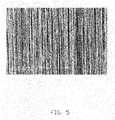
- FIG. 5is a Scanning Electron Microscope (SEM) image of a carbon nanotube film that can be utilized in the PDA.
- FIG. 6is a schematic structural view of a carbon nanotube segment.
- FIG. 7is a schematic cross-sectional view of the touch panel of the first embodiment used with a display screen, showing operation of the touch panel with a touch tool.
- FIG. 8is an exploded, isometric top view of a touch panel in the PDA according to a second embodiment.
- FIG. 9is a cross-sectional view of the touch panel of FIG. 8 taken along a line of VIII-VIII
- FIG. 10is a schematic cross-sectional view of the touch panel of the second embodiment used with a display screen, showing operation of the touch panel.
- the PDA 100includes a body 102 and a touch panel 10 .
- the body 102includes a display screen 104 .
- the touch panel 10is located on a surface of the display screen 104 .
- the body 102further includes a central processing unit (CPU) (not shown), a storage unit (not shown) and a control unit (not shown).
- the central processing unit, the storage unit, the control unit, and the display screen 104are all located in the body 102 .
- the storage unit, the central processing unit and the control unitcan be integrated on an integrated circuit board (not shown).
- the storage unit 170 and the control unit 150can be electrically connected to the central processing unit 160 by a conductive wire on the integrated circuit board.
- the display screen 104 and the touch panel 10are connected to the control unit 150 .
- the control unit 150can include a touch panel control unit, a display screen control unit and other functional control units used to correspondingly control the touch panel 10 , the display screen 104 , and other functions.
- the storage unit 170can be used to store data under control of the central processing unit.
- the storage unit 170can further include a read-only memory, a random access memory, and/or a programmable memory.
- the display screen 104can be selected from a group consisting of liquid crystal display screen, filed emission display screen and plasma display screen, electroluminescent display screen and vacuum fluorescent display screen.
- the display screen 104is a liquid crystal display screen.
- the display screen 104is located in the shell of the body 102 .
- the touch panel 10is configured for inputting signals.
- the touch panel 10can be spaced from the display screen 104 or installed directly on the display screen 104 .
- the touch panel 10can be adhered on the display screen 104 by an adhesive or the touch panel 10 and the display screen 104 are integrated, such as using a same base.
- the touch panel 10is installed directly on the display screen 104 .
- a keyboard(not shown) can be displayed on the display screen 104 .
- the touch panel 10can be a resistance-type or a capacitance-type touch panel.
- the touch panel 10 of the personal digital assistant 100is a resistance-type touch panel.
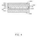
- the touch panel 10includes a first electrode plate 12 , a second electrode plate 14 , and a plurality of dot spacers 16 located between the first electrode plate 12 and the second electrode plate 14 .
- the first electrode plate 12includes a first substrate 120 , a first transparent conductive layer 122 , and two first-electrodes 124 .
- the first substrate 120includes a first surface 1202 and a second surface 1204 , each of which is substantially flat.
- the two first-electrodes 124 and the first transparent conductive layer 122are located on the first surface 1202 of the first substrate 120 .
- the two first-electrodes 124are located separately on opposite ends of the first transparent conductive layer 122 .
- a direction from one of the first-electrodes 124 across the first transparent conductive layer 122 to the other first electrode 124is defined as a first direction.
- the two first-electrodes 124are electrically connected to the first transparent conductive layer 122 .
- the second electrode plate 14includes a second substrate 140 as a support structure for a second transparent conductive layer 142 , and two second-electrodes 144 .
- the second substrate 140includes a first surface 1402 and a second surface 1404 , each of which is substantially flat.
- the two second-electrodes 144 and the second transparent conductive layer 142are located on the second surface 1404 of the second substrate 140 .
- the two second-electrodes 144are located separately on opposite ends of the second transparent conductive layer 142 .
- a direction from one of the second-electrodes 144 across the second transparent conductive layer 142 to the other second-electrodes 144is defined as a second direction, which is perpendicular to the first direction.
- the two second-electrodes 144are electrically connected to the second transparent conductive layer 142 . It is understood that when the touch panel 10 and the display screen 104 use a same base, the second transparent conductive layer 142 can be formed on a surface of the display screen 104 directly, and the second substrate 140 can be omitted.
- the first substrate 120is a transparent and flexible film or plate.
- the second substrate 140is a transparent plate.
- the first-electrodes 124 and the second-electrodes 144can be made of metal or any other suitable material.
- the first substrate 120is a polyester film
- the second substrate 140is a glass plate
- the first-electrodes 124 and second-electrodes 144are made of a conductive silver paste.
- An insulative layer 18is provided between the first and the second electrode plates 12 and 14 .
- the first electrode plate 12is located on the insulative layer 18 .
- the first transparent conductive layer 122is opposite to, but is spaced from, the second transparent conductive layer 142 .
- the dot spacers 16are separately located on the second transparent conductive layer 142 .
- a distance between the second electrode plate 14 and the first electrode plate 12can be in a range from about 2 to about 20 microns.
- the insulative layer 18 and the dot spacers 16are made of, for example, insulative resin or any other suitable insulative material. Therefore, insulation between the first electrode plate 12 and the second electrode plate 14 is provided by the insulative layer 18 and the dot spacers 16 .
- the dot spacers 16are optional, particularly when the touch panel 10 is relatively small. They serve as supports given the size of the span and the strength of the first electrode plate 12 and can be employed when needed.
- a transparent protective film 126is located on the second surface 1204 of the first substrate 120 of the first electrode plate 12 .
- the material of the transparent protective film 126can be selected from a group consisting of silicon nitrides, silicon dioxides, benzocyclobutenes, polyester films, and polyethylene terephthalates.
- the transparent protective film 126can be made of slick plastic and receive a surface hardening treatment to protect the first electrode plate 12 from being scratched when in use.
- At least one of the first transparent conductive layer 122 and the second transparent conductive layer 142includes a carbon nanotube layer.
- the carbon nanotube layeris substantially uniform in thickness and includes a plurality of carbon nanotubes uniformly distributed therein.
- the carbon nanotubes thereinare orderly or disorderly distributed.
- Disordered carbon nanotubesindicate a structure with carbon nanotubes arranged along many different directions, and the number of the carbon nanotubes in different directions is almost the same (e.g. uniform disorder).
- Ordered carbon nanotubesindicate a structure with carbon nanotubes arranged in consistently systematic manner, e.g., the carbon nanotubes are arranged approximately along a same direction or have two or more sections arranged approximately along a same direction.
- the carbon nanotube layerincludes at least one carbon nanotube film.
- the carbon nanotube filmcan be an ordered film or a disordered film. In the disordered film, the carbon nanotubes are disordered. The disordered film can be isotropic. The disordered carbon nanotubes are entangled with each other and/or attracted by van der Waals attractive therebetween.
- the carbon nanotubescan be substantially parallel to a surface of the carbon nanotube film. In the ordered film, the carbon nanotubes are primarily oriented along a same direction.
- the carbon nanotube layercan include at least two carbon nanotube films that overlap and/or stacked with each other.
- the carbon nanotube layeralso can include a plurality of coplanar carbon nanotube films.
- the plurality of coplanar carbon nanotube filmscan form a large area to make a large area touch panel.
- Carbon nanotubes in the carbon nanotube layercan be selected from a group consisting of single-walled, double-walled, and/or multi-walled carbon nanotubes. Diameters of the single-walled carbon nanotubes range from about 0.5 nanometers to about 50 nanometers. Diameters of the double-walled carbon nanotubes approximately range from about 1 nanometer to about 50 nanometers. Diameters of the multi-walled carbon nanotubes approximately range from about 1.5 nanometers to about 50 nanometers.
- carbon nanotubes in the carbon nanotube filmcan be in sections that are primarily aligned along the same direction.
- the directions in the different sectionscan be the same or different.
- the ordered filmcan be a drawn carbon nanotube film.
- the drawn carbon nanotube filmcan be formed by drawing from a carbon nanotube array. Referring to FIGS. 5 and 6 , the drawn carbon nanotube film can include a plurality of successively oriented carbon nanotube segments 143 joined end-to-end by van der Waals attractive force therebetween. Each carbon nanotube segment 143 includes a plurality of carbon nanotubes 145 parallel to each other, and combined by van der Waals attractive force therebetween.
- the carbon nanotube segments 143can vary in width, thickness, uniformity and shape.
- the carbon nanotubes 145 in the drawn carbon nanotube film 143are also oriented along a preferred orientation. A length and a width of the drawn carbon nanotube film can be arbitrarily set as desired.
- a thickness of the drawn carbon nanotube filmis in a range from about 0.5 nanometers to about 100 micrometers.
- the disordered filmcan be a flocculated carbon nanotube film.
- the flocculated carbon nanotube filmincludes a plurality of carbon nanotubes entangled with each other.
- a length of the carbon nanotubescan be a few microns to a few hundred microns.
- the adjacent carbon nanotubesare combined and entangled by van der Waals attractive force therebetween, thereby forming an entangled structure/microporous structure.
- the carbon nanotube filmis very microporous. Sizes of the micropores can be less than about 10 micrometers.
- carbon nanotube layer adopting the flocculated carbon nanotube film having a microporous structurecan have a high transparency. Thus it is conducive to use in the touch panel 10 .
- the ordered filmalso can be a pressed carbon nanotube film.
- the carbon nanotubes in the pressed carbon nanotube filmcan be overlapped with each other.
- the adjacent carbon nanotubesare combined and attracted by van der Waals attractive force, thereby forming a free-standing structure.
- the pressed carbon nanotube filmcan be formed by pressing a carbon nanotube array formed on a substrate.
- An angle between a primary alignment direction of the carbon nanotubes and the substratesuch that the angle is in a range from 0° to about 15°.
- the angleis closely related to pressure applied to the carbon nanotube array. The greater the pressure, the smaller the angle.
- the carbon nanotubes in the carbon nanotube pressed filmcan parallel to the surface of the pressed carbon nanotube film when the angle is 0°.
- the first transparent conductive layer 122 and the second transparent conductive layer 142both include a drawn carbon nanotube film.
- the drawn carbon nanotube filmincludes a plurality of successive and oriented carbon nanotube segments joined end to end by the van der Waals attractive force therebetween.
- the carbon nanotubes in the first transparent conductive layer 122can be oriented along a first direction
- the carbon nanotubes in the second transparent conductive layer 142can be oriented along a second, different direction. It is to be understood that some variation can occur in the orientation of the nanotubes in the drawn carbon nanotube film as can be seen in FIG. 5 .
- a thickness of the drawn carbon nanotube filmranges from about 0.5 nanometers to about 100 micrometers.
- a width of the drawn carbon nanotube filmranges from about 0.01 centimeters to about 10 meters.
- the touch panel 10can further include a shielding layer (not shown) located on the first surface 1402 of the second substrate 140 .
- the material of the shielding layercan be indium tin oxide, antimony tin oxide, carbon nanotube film, or other conductive materials.
- the shielding layeris a carbon nanotube film.
- the shielding layer carbon nanotube filmincludes a plurality of carbon nanotubes 145 , and the orientation of the carbon nanotubes 145 therein can be arbitrary or arranged along a same direction.
- the shielding layer carbon nanotube filmis connected to ground and plays a role of shielding and, thus, enables the touch panel 10 to operate without interference (e.g., electromagnetic interference).
- a passivation layer(not shown) can be further located on a surface of the shielding layer, on the side away from the second substrate 140 .
- the material of the passivation layercan, for example, be silicon nitride or silicon dioxide.
- the passivation layercan protect the shielding layer 22 from chemical or mechanical damage.
- 5Vare applied to each of the two first-electrodes 124 of the first electrode plate 12 and to each of the two second-electrodes 144 of the second electrode plate 14 .
- a useroperates the PDA 100 by pressing the first electrode plate 12 of the touch panel 10 with a finger, a pen/stylus 180 , or the like while visually observing the display screen 104 through the touch panel 10 .
- This pressingcauses a deformation of the first electrode plate 12 .
- the deformation of the first electrode plate 12causes a connection between the first transparent conductive layer 122 and the second conduction layer 142 of the second electrode plate 14 .
- Changes in voltages in the first direction of the first transparent conductive layer 142 and the second direction of the second transparent conductive layer 142can be detected by the touch panel controller of the control unit 150 . Then the control unit 150 transforms the changes in voltages into coordinates of the pressing point 182 , and sends the coordinates of the pressing point 182 to the central processing unit 160 .
- the central processing unit 160retrieves the command corresponding to the pressing point 182 from the storage unit 170 , and passes the command to the corresponding control unit of the control unit 150 .
- the control unit 150controls the display of the display screen 104 according to the command.
- the PDA 200includes a body and a touch panel 20 .
- the bodyincludes a display screen 204 .
- the touch panel 20is located on a surface of the display screen 204 .
- the bodyfurther includes a central processing unit (CPU) 260 , a storage unit 270 and a control unit 250 .
- the central processing unit 260 , the storage unit 270 , the control unit 250 , and the display screen 204are all located in the body.
- the storage unit 270 , the central processing unit 260 and the control unit 250can be integrated on an integrated circuit board (not shown).
- the storage unit 270 and the control unit 250can be electrically connected to the central processing unit 260 by a conductive wire on the integrated circuit board.
- the display screen 204 and the touch panel 20are connected to the control unit 250 .
- the control unit 250can include a touch panel control unit, a display screen control unit and other functional control units used to control the touch panel 20 , the display screen 204 and other functions and devices.
- the storage unit 270can be used to store the required data and operation results for the control of central processing unit.
- the storage unit 270can further include a read-only memory, a random access memory, and a
- the PDA 200 in the second embodimentis similar to the PDA 100 in the first embodiment. The difference is that, the touch panel 20 is a capacitance-type touch panel.
- the touch panel 20includes a substrate 22 , a transparent conductive layer 24 , a transparent protective layer 26 , and at least two electrodes 28 .
- the substrate 22has a first surface 221 and a second surface 222 at opposite sides thereof.
- the transparent conductive layer 24is located on the first surface 221 of the substrate 22 .
- the electrodes 28are located on the same side as the transparent conductive layer 24 and electrically connected with the transparent conductive layer 24 for forming an equipotential surface on the transparent conductive layer 24 .
- the transparent protective layer 26covers the electrodes 28 and the exposed surface of the transparent conductive layer 24 that faces away from the substrate 22 .
- the substrate 22has a planar structure or a curved structure.
- the material of the substrate 22can be selected from the group consisting of glass, quartz, diamond, and plastics. Understandably, the substrate 22 is made from a transparent material, e.g., either flexible or stiff, depending on whether a flexible device is desired or not.
- the substrate 22is used to support the transparent conductive layer 24 .
- the substrate 22can be the same as the first substrate 120 or second substrate 140 of the first embodiment.
- the transparent conductive layer 24includes a carbon nanotube layer.
- the carbon nanotube layerhas substantially a uniform thickness and includes a plurality of carbon nanotubes uniformly distributed therein.
- the carbon nanotubesare orderly or disorderly distributed in the carbon nanotube layer.
- the carbon nanotube layercan be the same as those disclosed in accordance with the first embodiment.
- the shape of the substrate 22 and the transparent conductive layer 24can be chosen according to the requirements of the touch filed of the touch panel 20 .
- the shape of the touch filedmay be triangular or rectangular, while other shapes can be used.
- the shapes of the touch filed, the substrate 22 , and the transparent conductive layer 24are all rectangular.
- the substrate 22is a glass substrate.
- the electrodes 28are strip-shaped and formed of silver, copper, or any alloy of at least one of such metals.
- the electrodes 28are located directly on a surface of the transparent conductive layer 24 that faces away from the substrate 22 .
- the electrodes 28are formed by one or more of spraying, electrical deposition, and electroless deposition methods.
- the electrodes 28can also be adhered to the surface of the transparent conductive layer 24 , e.g., by a silver-based slurry.
- the transparent protective layer 26is located on the electrodes 28 and the transparent conductive layer 24 .
- the material of the transparent protective layer 26can, e.g., be selected from a group consisting of silicon nitride, silicon dioxide, benzocyclobutenes, polyester film, and polyethylene terephthalate.
- the transparent protective layer 26can be a slick plastic film and receive a surface hardening treatment to protect the electrodes 28 and the transparent conductive layer 24 from being scratched when in use.
- the transparent protective layer 26is silicon dioxide.
- the hardness and thickness of the transparent protective layer 26are selected according to practical needs.
- the transparent protective layer 26is adhered to the transparent conductive layer 24 , e.g., via an adhesive.
- the touch panel 20can further include a shielding layer 230 located on the second surface 222 of the substrate 22 .
- the material of the shielding layer 230can be indium tin oxide, antimony tin oxide, carbon nanotube film, and/or another conductive material.
- the shielding layer 230is a carbon nanotube film.
- the shielding layer carbon nanotube filmincludes a plurality of carbon nanotubes, and the orientation of the carbon nanotubes therein may be arbitrarily determined.
- the carbon nanotubes in the shielding layer carbon nanotube filmare arranged along a same direction.
- the shielding layer carbon nanotube filmis connected to ground and acts as a shield, thus enabling the touch panel 20 to operate without interference (e.g., electromagnetic interference).
- a passivation layer 232can be located on and in contact with a surface of the shielding layer 230 that faces away from the substrate 22 .
- the material of the passivation layer 232can, for example, be silicon nitride or silicon dioxide.
- the passivation layer 232can protect the shielding layer 230 from chemical or mechanical damage.
- voltagesare applied to the electrodes 28 , by the control unit 250 .
- a useroperates the PDA 200 by pressing or touching the transparent protective layer 26 of the touch panel 20 with a touch tool (not shown), such as a finger, or an electrical pen/stylus, while visually observing the display screen 204 through the touch panel 20 .
- a coupling capacitanceforms between the user and the transparent conductive layer 24 .
- the coupling capacitanceis a conductor, and thus the touch tool takes away a little current from the touch point. Currents flowing through the four electrodes 28 cooperatively replace the current lost at the touch point.
- the quantity of current supplied by each electrode 28is directly proportional to the distances from the touch point to the electrodes 28 .
- the touch panel control unit in the control unit 250is used to calculate the proportion of the four supplied currents, thereby detecting coordinates of the touch point on the touch panel 20 . Then, the control unit 250 sends the coordinates of the touch point to the central processing unit 260 .
- the central processing unit 260accepts the coordinates of the touch point, takes out the command corresponding to the pressing point from the storage unit 270 , and passes it to the corresponding control unit of the control unit 250 .
- the control unit 250controls the display of the display screen 204 according to the command.
- the PDA employing the carbon nanotube filmhas a high transparency, thereby promoting improved brightness to the PDA.
Landscapes
- Engineering & Computer Science (AREA)
- Theoretical Computer Science (AREA)
- General Engineering & Computer Science (AREA)
- Computer Hardware Design (AREA)
- Human Computer Interaction (AREA)
- Physics & Mathematics (AREA)
- General Physics & Mathematics (AREA)
- Position Input By Displaying (AREA)
- Carbon And Carbon Compounds (AREA)
Abstract
Description
Claims (18)
Applications Claiming Priority (3)
| Application Number | Priority Date | Filing Date | Title |
|---|---|---|---|
| CN2008101420230ACN101655720B (en) | 2008-08-22 | 2008-08-22 | Personal digital assistant |
| CN200810142023.0 | 2008-08-22 | ||
| CN200810142023 | 2008-08-22 |
Publications (2)
| Publication Number | Publication Date |
|---|---|
| US20100048250A1 US20100048250A1 (en) | 2010-02-25 |
| US8346316B2true US8346316B2 (en) | 2013-01-01 |
Family
ID=41696870
Family Applications (1)
| Application Number | Title | Priority Date | Filing Date |
|---|---|---|---|
| US12/384,328Expired - Fee RelatedUS8346316B2 (en) | 2008-08-22 | 2009-04-02 | Personal digital assistant |
Country Status (3)
| Country | Link |
|---|---|
| US (1) | US8346316B2 (en) |
| JP (1) | JP2010049691A (en) |
| CN (1) | CN101655720B (en) |
Cited By (5)
| Publication number | Priority date | Publication date | Assignee | Title |
|---|---|---|---|---|
| US20100007625A1 (en)* | 2008-07-09 | 2010-01-14 | Tsinghua University | Touch panel, liquid crystal display screen using the same, and methods for making the touch panel and the liquid crystal display screen |
| US20100317409A1 (en)* | 2009-06-12 | 2010-12-16 | Tsinghua University | Carbon nanotube based flexible mobile phone |
| US20140022497A1 (en)* | 2012-07-23 | 2014-01-23 | Tianjin Funayuanchuang Technology Co.,Ltd. | Liquid crystal display module |
| US20140022464A1 (en)* | 2012-07-23 | 2014-01-23 | Tianjin Funayuanchuang Technology Co.,Ltd. | Liquid crystal display module |
| US8982301B2 (en)* | 2012-07-23 | 2015-03-17 | Tianjin Funayuanchuang Technology Co., Ltd. | Method for making liquid crystal display module |
Families Citing this family (12)
| Publication number | Priority date | Publication date | Assignee | Title |
|---|---|---|---|---|
| JP2011017626A (en)* | 2009-07-09 | 2011-01-27 | Sony Corp | Mechanical quantity detection member and mechanical quantity detection apparatus |
| USD641332S1 (en)* | 2010-01-06 | 2011-07-12 | Sony Ericsson Mobile Communications Ab | Mobile phone |
| CN101880035A (en) | 2010-06-29 | 2010-11-10 | 清华大学 | carbon nanotube structure |
| USD687024S1 (en)* | 2010-07-06 | 2013-07-30 | Sony Corporation | Information terminal |
| FR2963445B1 (en)* | 2010-08-02 | 2013-05-03 | Nanomade Concept | TOUCH SURFACE AND METHOD FOR MANUFACTURING SUCH SURFACE |
| USD645437S1 (en)* | 2010-11-16 | 2011-09-20 | Cheng Uei Precision Industry Co., Ltd. | Mobile phone |
| KR101330809B1 (en)* | 2011-08-03 | 2013-12-19 | 주식회사 팬택 | Touch panel and electronic device including the touch panel |
| TWI581135B (en)* | 2011-09-30 | 2017-05-01 | 加拿都公司 | Touch sensitive film, touch sensing device, and electronic device |
| USD716796S1 (en)* | 2012-12-12 | 2014-11-04 | Americhip, Inc. | Video tablet |
| USD756355S1 (en)* | 2013-11-20 | 2016-05-17 | Fujifilm Corporation | Personal digital assistance |
| USD756354S1 (en)* | 2013-11-20 | 2016-05-17 | Fujifilm Corporation | Personal digital assistance |
| WO2018051708A1 (en)* | 2016-09-13 | 2018-03-22 | コニカミノルタ株式会社 | Illuminating device |
Citations (176)
| Publication number | Priority date | Publication date | Assignee | Title |
|---|---|---|---|---|
| JPS61231626A (en) | 1985-04-05 | 1986-10-15 | Asahi Chem Ind Co Ltd | Conductive sheet for position detection |
| JPS6263332U (en) | 1985-10-11 | 1987-04-20 | ||
| US4659873A (en) | 1985-07-19 | 1987-04-21 | Elographics, Inc. | Fabric touch sensor and method of manufacture |
| JPS62182916U (en) | 1986-05-08 | 1987-11-20 | ||
| JPS62190524U (en) | 1986-05-26 | 1987-12-04 | ||
| US4922061A (en) | 1988-06-13 | 1990-05-01 | Tektronix, Inc. | Capacitive touch panel system with randomly modulated position measurement signal |
| US4933660A (en) | 1989-10-27 | 1990-06-12 | Elographics, Inc. | Touch sensor with touch pressure capability |
| US5181030A (en) | 1989-12-28 | 1993-01-19 | Gunze Limited | Input system including resistance film touch panel and pushed position detecting device |
| JPH0628090Y2 (en) | 1992-06-03 | 1994-08-03 | 健一 古谷 | Electrode structure in used needle processing equipment |
| TW242732B (en) | 1993-06-29 | 1995-03-11 | Victor Company Of Japan | Digital chrominance signal processing circuit |
| TW284963B (en) | 1995-02-17 | 1996-09-01 | Nippon Tobacco Sangyo Kk | |
| TW284927B (en) | 1993-05-27 | 1996-09-01 | Mabuchi Motor Co | |
| JPH1063404A (en) | 1996-08-27 | 1998-03-06 | Matsushita Electric Ind Co Ltd | Coordinate position input device |
| TW341684B (en) | 1996-07-15 | 1998-10-01 | Synaptics Inc | Object position detector |
| US5853877A (en) | 1996-05-31 | 1998-12-29 | Hyperion Catalysis International, Inc. | Method for disentangling hollow carbon microfibers, electrically conductive transparent carbon microfibers aggregation film amd coating for forming such film |
| US5861583A (en) | 1992-06-08 | 1999-01-19 | Synaptics, Incorporated | Object position detector |
| US5931764A (en) | 1998-06-24 | 1999-08-03 | Viztec, Inc. | Wearable device with flexible display |
| JP2001267782A (en) | 2000-03-21 | 2001-09-28 | Shimadzu Corp | Electromagnetic wave absorption shielding material |
| US6373472B1 (en) | 1995-10-13 | 2002-04-16 | Silviu Palalau | Driver control interface system |
| US20020089492A1 (en) | 2001-01-11 | 2002-07-11 | Young-Soo Ahn | Flat panel display with input device |
| US6423583B1 (en) | 2001-01-03 | 2002-07-23 | International Business Machines Corporation | Methodology for electrically induced selective breakdown of nanotubes |
| TW498266B (en) | 2000-08-03 | 2002-08-11 | Hantouch Com | Resistive film type transparent analog touch panel |
| JP2002278701A (en) | 2001-03-21 | 2002-09-27 | Nissha Printing Co Ltd | Touch panel |
| WO2002076724A1 (en) | 2001-03-26 | 2002-10-03 | Eikos, Inc. | Coatings containing carbon nanotubes |
| TW508652B (en) | 2001-10-03 | 2002-11-01 | Taiwan Semiconductor Mfg | Device and method for wafer drying |
| TW521227B (en) | 2000-03-31 | 2003-02-21 | Sharp Kk | Electrode substrate, method for producing the same and display device including the same |
| CN2539375Y (en) | 2002-04-15 | 2003-03-05 | 湖南三才光电信息材料有限公司 | High-stable flexible transparent conducting composite film |
| US20030122800A1 (en) | 2001-12-27 | 2003-07-03 | Lg, Philips Lcd Co., Ltd. | Touch panel liquid crystal display device and method of fabricating the same |
| US20030147041A1 (en) | 2001-12-27 | 2003-08-07 | Lg.Philips Lcd Co., Ltd | Method of fabricating liquid crystal display apparatus integrated with film type touch panel |
| US6628269B2 (en) | 2000-02-10 | 2003-09-30 | Nec Corporation | Touch panel input device capable of sensing input operation using a pen and a fingertip and method therefore |
| US6629833B1 (en) | 1998-05-15 | 2003-10-07 | Toyo Boseki Kabushiki Kaisha | Transparent conductive film and touch panel |
| CN1447279A (en) | 2003-03-18 | 2003-10-08 | 中国电子科技集团公司第五十五研究所 | High reliable touch screen and manufacturing technique |
| US20030189235A1 (en) | 2002-04-09 | 2003-10-09 | Hiroyuki Watanabe | Photoelectric conversion element and photoelectric conversion device |
| TW200403498A (en) | 2002-08-20 | 2004-03-01 | Samsung Electronics Co Ltd | Light guide plate and liquid crystal display having the same |
| US20040047038A1 (en) | 2002-09-10 | 2004-03-11 | Kai-Li Jiang | Optical polarizer and method for fabricating such optical polarizer |
| US20040053780A1 (en) | 2002-09-16 | 2004-03-18 | Jiang Kaili | Method for fabricating carbon nanotube yarn |
| US20040099438A1 (en) | 2002-05-21 | 2004-05-27 | Arthur David J. | Method for patterning carbon nanotube coating and carbon nanotube wiring |
| CN1501317A (en) | 2002-11-14 | 2004-06-02 | Lg.������Lcd����˾ | display device touch screen |
| CN1503195A (en) | 2002-11-20 | 2004-06-09 | Lg.������Lcd��ʽ���� | Digital Resistive Touch Panel |
| CN1509982A (en) | 2002-12-21 | 2004-07-07 | �廪��ѧ | A carbon nanotube array structure and its growth method |
| JP2004189573A (en) | 2002-12-13 | 2004-07-08 | Jfe Engineering Kk | Aggregate of carbon nanotubes and carbon nanotube installation device having the same |
| CN1519196A (en) | 2003-01-23 | 2004-08-11 | 南昌大学 | Fabrication method of aligned carbon nanotube film on soft substrate |
| CN2638143Y (en) | 2003-05-24 | 2004-09-01 | 江阴市华丽计算机网络工程有限公司 | Multifunctional PDA |
| JP2004253796A (en) | 2003-01-31 | 2004-09-09 | Takiron Co Ltd | Electromagnetic wave shielding structure |
| JP2004266272A (en) | 2003-02-14 | 2004-09-24 | Toray Ind Inc | Field effect transistor and liquid crystal display device using the same |
| US20040191157A1 (en) | 2003-03-31 | 2004-09-30 | Avetik Harutyunyan | Method for selective enrichment of carbon nanotubes |
| US20040251504A1 (en) | 2003-05-07 | 2004-12-16 | Sony Corporation | Field effect transistor and method for manufacturing the same |
| US20050110720A1 (en) | 2003-11-21 | 2005-05-26 | Hitachi Displays, Ltd. | Image display device |
| TWI233570B (en) | 2001-12-28 | 2005-06-01 | Lg Philips Lcd Co Ltd | Touch panel display apparatus and method of fabricating the same |
| CN2706973Y (en) | 2004-06-30 | 2005-06-29 | 陈凯 | Fingers-nipping gloves cell phone |
| JP2005176428A (en) | 2003-12-08 | 2005-06-30 | Japan Science & Technology Agency | Actuator element |
| TW200522366A (en) | 2003-11-19 | 2005-07-01 | Seiko Epson Corp | Method of manufacturing a thin film transistor, thin film transistor, thin film transistor circuit, electronic device, and electronic apparatus |
| JP2005182339A (en) | 2003-12-18 | 2005-07-07 | Kawaguchiko Seimitsu Co Ltd | Touch panel and screen input type display device therewith |
| JP2005222182A (en) | 2004-02-04 | 2005-08-18 | Citizen Watch Co Ltd | Position inputting device |
| US6947203B2 (en) | 2003-06-24 | 2005-09-20 | Seiko Epson Corporation | Electrophoretic dispersion, electrophoretic display device, method of manufacturing electrophoretic display device, and electronic system |
| US20050209392A1 (en) | 2003-12-17 | 2005-09-22 | Jiazhong Luo | Polymer binders for flexible and transparent conductive coatings containing carbon nanotubes |
| JP2005286158A (en) | 2004-03-30 | 2005-10-13 | Seiko Epson Corp | PATTERN FORMING METHOD, ELECTRONIC DEVICE, ITS MANUFACTURING METHOD, AND ELECTRONIC DEVICE |
| CN1690915A (en) | 2004-04-28 | 2005-11-02 | 秦建忠 | Double screen notebook computer |
| WO2005104141A1 (en) | 2004-04-20 | 2005-11-03 | Takiron Co., Ltd. | Touch panel-use transparent conductive molded product and touch panel |
| WO2005102924A1 (en) | 2004-04-19 | 2005-11-03 | Japan Science And Technology Agency | Carbon-based fine structure group, aggregate of carbon based fine structures, use thereof and method for preparation thereof |
| WO2006003245A1 (en) | 2004-07-06 | 2006-01-12 | Upm-Kymmene Corporation | Sensor product for electric field sensing |
| US20060010996A1 (en) | 2004-07-13 | 2006-01-19 | United States Of America As Represented By The Administrator Of The Nasa | Carbon nanotube-based sensor and method for continually sensing changes in a structure |
| US20060022221A1 (en) | 2004-07-29 | 2006-02-02 | International Business Machines Corporation | Integrated circuit chip utilizing oriented carbon nanotube conductive layers |
| TWI249134B (en) | 2003-07-23 | 2006-02-11 | Wintek Corp | Touch panel structure |
| TWI249708B (en) | 2004-09-09 | 2006-02-21 | Ind Tech Res Inst | Analog resistive touch panel without bias |
| CN1738018A (en) | 2005-08-18 | 2006-02-22 | 上海交通大学 | Method for Bonding Nanomaterials to Metal Electrodes |
| US20060044284A1 (en) | 2004-09-02 | 2006-03-02 | Koji Tanabe | Touch panel and the manufacturing method |
| CN1745302A (en) | 2003-01-30 | 2006-03-08 | 艾考斯公司 | Articles with dispersed conductive coatings |
| WO2006030981A1 (en) | 2004-09-17 | 2006-03-23 | National Institute Of Advanced Industrial Scienceand Technology | Transparent conductive carbon nanotube film and method for producing same |
| US20060077147A1 (en)* | 2004-09-27 | 2006-04-13 | Lauren Palmateer | System and method for protecting micro-structure of display array using spacers in gap within display device |
| TWI253846B (en) | 2005-03-28 | 2006-04-21 | Ind Tech Res Inst | Photo-sensing display unit |
| US20060097991A1 (en)* | 2004-05-06 | 2006-05-11 | Apple Computer, Inc. | Multipoint touchscreen |
| JP2006171336A (en) | 2004-12-15 | 2006-06-29 | Takiron Co Ltd | Transparent electrode member for image display, and the image display device |
| TW200622432A (en) | 2004-12-31 | 2006-07-01 | Hon Hai Prec Ind Co Ltd | Liquid crystal display device |
| US7071927B2 (en) | 1999-11-17 | 2006-07-04 | L-3 Communications Corporation | Resistive touch panel using removable, tensioned top layer |
| CN1803594A (en) | 2005-11-25 | 2006-07-19 | 清华大学 | Large-area ultra-thin carbon nanotube film and its preparation process |
| TWI258708B (en) | 2005-01-27 | 2006-07-21 | Apex Material Technology Corp | Resistive touch panel, and it manufacturing method |
| US20060171032A1 (en) | 2005-01-07 | 2006-08-03 | Kimihiko Nishioka | Medium exhibiting negative refraction, optical element, and optical system |
| CN1823320A (en) | 2003-06-14 | 2006-08-23 | 罗纳德·P·宾斯蒂德 | Improvements in touch technology |
| US20060188721A1 (en) | 2005-02-22 | 2006-08-24 | Eastman Kodak Company | Adhesive transfer method of carbon nanotube layer |
| US20060187369A1 (en) | 2004-05-13 | 2006-08-24 | Quanta Display Inc. | Liquid crystal display without storage capacitance electrode lines |
| US20060187213A1 (en) | 2005-02-21 | 2006-08-24 | Au Optronics Corp. | Electroluminescence display with touch panel |
| JP2006228818A (en) | 2005-02-15 | 2006-08-31 | Fujitsu Ltd | Method for forming carbon nanotube and method for manufacturing electronic device |
| JP2006243455A (en) | 2005-03-04 | 2006-09-14 | C's Lab Ltd | Map display method, map display program, and map display device |
| US20060213251A1 (en) | 2005-03-24 | 2006-09-28 | University Of Florida Research Foundation, Inc. | Carbon nanotube films for hydrogen sensing |
| JP2006269311A (en) | 2005-03-25 | 2006-10-05 | Toray Ind Inc | Transparent conductive film containing carbon nano-tube obtained by making metal-carrying carrier contact with carbon-containing organic compound |
| JP2006285068A (en) | 2005-04-04 | 2006-10-19 | Nikkiso Co Ltd | Conductive polarizing film |
| US20060240605A1 (en) | 2005-04-22 | 2006-10-26 | Hee-Sung Moon | Organic thin film transistor and method of fabricating the same |
| WO2006120803A1 (en) | 2005-05-10 | 2006-11-16 | Sumitomo Precision Products Co., Ltd | Highly thermally conductive composite material |
| US20060263588A1 (en) | 2005-04-28 | 2006-11-23 | Bussan Nanotech Research Institute Inc. | Transparent conductive film and coating composition therefor |
| US20060262055A1 (en) | 2005-01-26 | 2006-11-23 | Toshiba Matsushita Display Technology | Plane display device |
| WO2006126604A1 (en) | 2005-05-26 | 2006-11-30 | Gunze Limited | Transparent planar body and transparent touch switch |
| CN2844974Y (en) | 2005-12-08 | 2006-12-06 | 比亚迪股份有限公司 | Contact style liquid crystal display device |
| US20060274048A1 (en)* | 2005-06-02 | 2006-12-07 | Eastman Kodak Company | Touchscreen with conductive layer comprising carbon nanotubes |
| US20060275956A1 (en) | 2005-06-04 | 2006-12-07 | Gregory Konesky | Cross-linked carbon nanotubes |
| US20060274047A1 (en) | 2005-06-02 | 2006-12-07 | Eastman Kodak Company | Touchscreen with one carbon nanotube conductive layer |
| US20060274049A1 (en) | 2005-06-02 | 2006-12-07 | Eastman Kodak Company | Multi-layer conductor with carbon nanotubes |
| KR20060129977A (en) | 2006-09-08 | 2006-12-18 | 아이티엠 주식회사 | Highly durable resistive touch screen panel and its manufacturing method |
| CN1903793A (en) | 2005-07-26 | 2007-01-31 | 中国科学院物理研究所 | Carbon silicon composite material, its preparation method and use |
| WO2007012899A1 (en) | 2005-07-25 | 2007-02-01 | Plastic Logic Limited | Flexible touch screen display |
| TWM306694U (en) | 2006-03-15 | 2007-02-21 | Ushine Photonics Corp | Durable resistive touch screen |
| TW200710493A (en) | 2005-05-23 | 2007-03-16 | Ran-Hong Wang | Controlling polarization for liquid crystal displays |
| US7196463B2 (en) | 2003-08-06 | 2007-03-27 | Hitachi Displays, Ltd. | Emissive flat panel display having electron sources with high current density and low electric field strength |
| TW200713337A (en) | 2005-07-07 | 2007-04-01 | 3M Innovative Properties Co | Touch panel sensor |
| US20070075619A1 (en) | 2005-09-30 | 2007-04-05 | Tsinghua University | Field emission device and method for making the same |
| US20070081681A1 (en) | 2005-10-03 | 2007-04-12 | Xun Yu | Thin film transparent acoustic transducer |
| CN1948144A (en) | 2006-11-10 | 2007-04-18 | 清华大学 | Ultralong orientational carbon nano-tube filament/film and its preparation method |
| US20070085838A1 (en) | 2005-10-17 | 2007-04-19 | Ricks Theodore K | Method for making a display with integrated touchscreen |
| TW200717083A (en) | 2005-10-28 | 2007-05-01 | Hon Hai Prec Ind Co Ltd | Liquid crystal display and its manufacturing method |
| US20070099333A1 (en) | 2003-07-17 | 2007-05-03 | Seiko Epson Corporation | Thin-film transistor, method of producing thin-film transistor, electronic circuit, display, and electronic device |
| US7215329B2 (en) | 2001-10-10 | 2007-05-08 | Smk Corporation | Touch panel input device |
| CN1315362C (en) | 2003-06-27 | 2007-05-09 | 中国科学院上海硅酸盐研究所 | Carbon nano-pipe/ceramic composite material possessing microwave absorption function and its preparation method |
| JP2007112133A (en) | 2003-01-30 | 2007-05-10 | Takiron Co Ltd | Electroconductive shaped article |
| TW200719198A (en) | 2005-06-16 | 2007-05-16 | Nissha Printing | Housing component with illuminated switch and method of producing the same |
| JP2007123870A (en) | 2005-09-29 | 2007-05-17 | Matsushita Electric Ind Co Ltd | Flat panel display device and manufacturing method thereof |
| WO2007063751A1 (en) | 2005-11-29 | 2007-06-07 | Seiko Instruments Inc. | Process for producing display and method of laminating |
| WO2007066649A1 (en) | 2005-12-06 | 2007-06-14 | Mitsubishi Rayon Co., Ltd. | Carbon nanotube-containing composition, composite body, and their production methods |
| TW200722559A (en) | 2005-12-06 | 2007-06-16 | Ind Tech Res Inst | Metal nanodot arrays and fabrication methods thereof |
| CN1982209A (en) | 2005-12-16 | 2007-06-20 | 清华大学 | Carbon nano-tube filament and its production |
| WO2007022226A3 (en) | 2005-08-12 | 2007-06-21 | Cambrios Technologies Corp | Nanowires-based transparent conductors |
| JP2007161576A (en) | 2005-12-09 | 2007-06-28 | Kofukin Seimitsu Kogyo (Shenzhen) Yugenkoshi | Method for producing carbon nanotube array |
| US7242136B2 (en) | 2003-03-11 | 2007-07-10 | Lg Electronics Inc. | Front filter, and plasma display apparatus having the same |
| CN1996620A (en) | 2006-12-29 | 2007-07-11 | 清华大学 | Carbon nano tube film-based solar energy battery and its preparing method |
| TW200727163A (en) | 2006-01-06 | 2007-07-16 | Pan Jit Internat Inc | Antibacterial touch display device |
| US20070165004A1 (en) | 2006-01-17 | 2007-07-19 | World Properties, Inc. | Capacitive touch sensor with integral EL backlight |
| JP2007182546A (en) | 2005-12-06 | 2007-07-19 | Mitsubishi Rayon Co Ltd | Carbon nanotube-containing composition, composite, and production method thereof |
| JP2007182357A (en) | 2006-01-10 | 2007-07-19 | Nok Corp | Aftertreatment method of carbon material thin film |
| US20070182720A1 (en) | 2006-02-07 | 2007-08-09 | Shoji Fujii | Touch panel |
| KR20070081902A (en) | 2006-02-14 | 2007-08-20 | 삼성전자주식회사 | Liquid crystal display |
| DE202007006407U1 (en) | 2006-05-05 | 2007-09-06 | Philipp, Harald | Touch screen element |
| WO2007099975A1 (en) | 2006-02-28 | 2007-09-07 | Toyo Boseki Kabushiki Kaisha | Carbon nanotube assembly, carbon nanotube fiber and process for producing carbon nanotube fiber |
| JP2007229989A (en) | 2006-02-28 | 2007-09-13 | Takiron Co Ltd | Conductive molded body and its manufacturing method |
| US20070215841A1 (en) | 2004-05-14 | 2007-09-20 | Sonydeutschland Gmbh | Composite Materials Comprising Carbon Nanotubes and Metal Carbonates |
| TW200737414A (en) | 2006-03-23 | 2007-10-01 | Unimicron Technology Corp | Carbon nanotube field emitting display |
| TW200736979A (en) | 2006-03-17 | 2007-10-01 | Innolux Display Corp | Touch panel |
| TW200738558A (en) | 2006-01-03 | 2007-10-16 | Nano Proprietary Inc | Curing binder material for carbon nanotube electron emission cathodes |
| CN101059738A (en) | 2006-04-20 | 2007-10-24 | 铼宝科技股份有限公司 | Transparent touch screen with upward-emitting organic light-emitting diodes |
| JP2007310869A (en) | 2006-04-17 | 2007-11-29 | Matsushita Electric Ind Co Ltd | Input device control method and input device used therefor |
| US20070279556A1 (en) | 2005-05-23 | 2007-12-06 | Wang Ran-Hong R | Controlling polarization for liquid crystal displays |
| US20070296897A1 (en) | 2006-06-23 | 2007-12-27 | Tsinghua University | Liquid crystal cell assembly for liquid crystal display |
| US20080048996A1 (en) | 2006-08-11 | 2008-02-28 | Unidym, Inc. | Touch screen devices employing nanostructure networks |
| US7355592B2 (en) | 2002-12-24 | 2008-04-08 | Lg.Philips Lcd Co., Ltd. | Digital resistive type touch panel and fabrication method thereof |
| US20080088219A1 (en) | 2006-10-17 | 2008-04-17 | Samsung Electronics Co., Ltd. | Transparent carbon nanotube electrode using conductive dispersant and production method thereof |
| JP2008102968A (en) | 2007-12-28 | 2008-05-01 | Fujitsu Component Ltd | Touch panel |
| US20080129666A1 (en) | 2006-12-05 | 2008-06-05 | Susumu Shimotono | Method and Apparatus for Changing a Display Direction of a Screen of a Portable Electronic Device |
| US20080192014A1 (en) | 2007-02-08 | 2008-08-14 | Tyco Electronics Corporation | Touch screen using carbon nanotube electrodes |
| US20080238882A1 (en)* | 2007-02-21 | 2008-10-02 | Ramesh Sivarajan | Symmetric touch screen system with carbon nanotube-based transparent conductive electrode pairs |
| US20080248235A1 (en) | 2007-02-09 | 2008-10-09 | Tsinghua University | Carbon nanotube film structure and method for fabricating the same |
| US20080266273A1 (en) | 2007-04-24 | 2008-10-30 | White Electronic Designs Corp. | Interactive display system |
| US20090032777A1 (en) | 2005-06-07 | 2009-02-05 | Kuraray Co., Ltd. | Carbon nanotube dispersion liquid and transparent conductive film using same |
| US20090059151A1 (en) | 2007-09-03 | 2009-03-05 | Samsung Electronics Co., Ltd. | Liquid crystal display panel and manufacturintg method therreof |
| US20090056854A1 (en) | 2006-04-04 | 2009-03-05 | Top-Nanosis, Inc. | Method for manufacturing conductive composite material |
| US20090101488A1 (en) | 2007-10-23 | 2009-04-23 | Tsinghua University | Touch panel |
| JP2009104577A (en) | 2007-10-23 | 2009-05-14 | Kofukin Seimitsu Kogyo (Shenzhen) Yugenkoshi | Touch panel |
| US20090153511A1 (en) | 2007-12-12 | 2009-06-18 | Tsinghua University | Touch panel and display device using the same |
| US20090153513A1 (en) | 2007-12-14 | 2009-06-18 | Tsinghua University | Touch panel, method for making the same, and display device adopting the same |
| US20090153516A1 (en) | 2007-12-12 | 2009-06-18 | Tsinghua University | Touch panel, method for making the same, and display device adopting the same |
| TW200929638A (en) | 2007-12-21 | 2009-07-01 | Hon Hai Prec Ind Co Ltd | Touch panel, method for making the same, and displaying device adopting the same |
| TW200928914A (en) | 2007-12-31 | 2009-07-01 | Hon Hai Prec Ind Co Ltd | Touch panel and displaying device using the same |
| TW200929643A (en) | 2007-12-21 | 2009-07-01 | Hon Hai Prec Ind Co Ltd | Touch panel, method for making the same, and displaying device adopting the same |
| US20090167709A1 (en) | 2007-12-27 | 2009-07-02 | Tsinghua University | Touch panel and display device using the same |
| US20090293631A1 (en) | 2008-05-29 | 2009-12-03 | Zoran Radivojevic | Flexural deformation sensing device and a user interface using the same |
| US7630040B2 (en) | 2005-10-27 | 2009-12-08 | Tsinghua University | Liquid crystal display and manufacturing method therefor comprising alignment films of oriented carbon nanotubes |
| US20100001972A1 (en) | 2008-07-04 | 2010-01-07 | Tsinghua University | Touch Panel |
| US20100001975A1 (en) | 2008-07-04 | 2010-01-07 | Tsinghua University | Portable computer |
| US20100007619A1 (en) | 2008-07-09 | 2010-01-14 | Tsinghua University | Touch panel, liquid crystal display screen using the same, and methods for making the touch panel and the liquid crystal display screen |
| TW201005612A (en) | 2008-07-25 | 2010-02-01 | Hon Hai Prec Ind Co Ltd | Portable computer |
| US7662732B2 (en)* | 2006-05-26 | 2010-02-16 | Samsung Electronics Co., Ltd. | Method of preparing patterned carbon nanotube array and patterned carbon nanotube array prepared thereby |
| US7710649B2 (en) | 2007-03-30 | 2010-05-04 | Tsinghua University | Optical polarizer and method for fabricating the same |
| US20100171099A1 (en) | 2004-09-16 | 2010-07-08 | Atomate Corporation | Carbon Nanotube Transistor Structure |
| CN1998067B (en) | 2004-07-06 | 2010-07-14 | 毫微-专卖股份有限公司 | Activation of carbon nanotubes in field emission applications |
| US7796123B1 (en) | 2006-06-20 | 2010-09-14 | Eastman Kodak Company | Touchscreen with carbon nanotube conductive layers |
| US7825911B2 (en)* | 2006-03-27 | 2010-11-02 | Sanyo Electric Co., Ltd. | Touch sensor, touch pad and input device |
| US7854992B2 (en) | 2007-04-06 | 2010-12-21 | Tsinghua University | Conductive tape and method for making the same |
| US20110032196A1 (en) | 2009-08-07 | 2011-02-10 | Tsinghua University | Touch panel and display device using the same |
| US7947977B2 (en) | 2008-05-14 | 2011-05-24 | Tsinghua University | Thin film transistor |
Family Cites Families (3)
| Publication number | Priority date | Publication date | Assignee | Title |
|---|---|---|---|---|
| KR100456019B1 (en)* | 2002-07-02 | 2004-11-08 | 삼성전자주식회사 | Lcd assembly of pda |
| JP2005028821A (en)* | 2003-07-10 | 2005-02-03 | Sony Corp | Transparent conductive base and touch panel |
| JP2007011997A (en)* | 2005-07-04 | 2007-01-18 | Fujitsu Component Ltd | Touch panel |
- 2008
- 2008-08-22CNCN2008101420230Apatent/CN101655720B/ennot_activeExpired - Fee Related
- 2009
- 2009-04-02USUS12/384,328patent/US8346316B2/ennot_activeExpired - Fee Related
- 2009-08-24JPJP2009193178Apatent/JP2010049691A/enactivePending
Patent Citations (243)
| Publication number | Priority date | Publication date | Assignee | Title |
|---|---|---|---|---|
| JPS61231626A (en) | 1985-04-05 | 1986-10-15 | Asahi Chem Ind Co Ltd | Conductive sheet for position detection |
| US4659873A (en) | 1985-07-19 | 1987-04-21 | Elographics, Inc. | Fabric touch sensor and method of manufacture |
| JPS6263332U (en) | 1985-10-11 | 1987-04-20 | ||
| JPS62182916U (en) | 1986-05-08 | 1987-11-20 | ||
| JPS62190524U (en) | 1986-05-26 | 1987-12-04 | ||
| US4922061A (en) | 1988-06-13 | 1990-05-01 | Tektronix, Inc. | Capacitive touch panel system with randomly modulated position measurement signal |
| US4933660A (en) | 1989-10-27 | 1990-06-12 | Elographics, Inc. | Touch sensor with touch pressure capability |
| US5181030A (en) | 1989-12-28 | 1993-01-19 | Gunze Limited | Input system including resistance film touch panel and pushed position detecting device |
| JPH0628090Y2 (en) | 1992-06-03 | 1994-08-03 | 健一 古谷 | Electrode structure in used needle processing equipment |
| US5861583A (en) | 1992-06-08 | 1999-01-19 | Synaptics, Incorporated | Object position detector |
| TW284927B (en) | 1993-05-27 | 1996-09-01 | Mabuchi Motor Co | |
| TW242732B (en) | 1993-06-29 | 1995-03-11 | Victor Company Of Japan | Digital chrominance signal processing circuit |
| TW284963B (en) | 1995-02-17 | 1996-09-01 | Nippon Tobacco Sangyo Kk | |
| US6373472B1 (en) | 1995-10-13 | 2002-04-16 | Silviu Palalau | Driver control interface system |
| US5853877A (en) | 1996-05-31 | 1998-12-29 | Hyperion Catalysis International, Inc. | Method for disentangling hollow carbon microfibers, electrically conductive transparent carbon microfibers aggregation film amd coating for forming such film |
| TW341684B (en) | 1996-07-15 | 1998-10-01 | Synaptics Inc | Object position detector |
| JPH1063404A (en) | 1996-08-27 | 1998-03-06 | Matsushita Electric Ind Co Ltd | Coordinate position input device |
| US6629833B1 (en) | 1998-05-15 | 2003-10-07 | Toyo Boseki Kabushiki Kaisha | Transparent conductive film and touch panel |
| US5931764A (en) | 1998-06-24 | 1999-08-03 | Viztec, Inc. | Wearable device with flexible display |
| JP2002519754A (en) | 1998-06-24 | 2002-07-02 | ビズテック インコーポレイテッド | Wearing device with flexible display |
| US7071927B2 (en) | 1999-11-17 | 2006-07-04 | L-3 Communications Corporation | Resistive touch panel using removable, tensioned top layer |
| US6628269B2 (en) | 2000-02-10 | 2003-09-30 | Nec Corporation | Touch panel input device capable of sensing input operation using a pen and a fingertip and method therefore |
| JP2001267782A (en) | 2000-03-21 | 2001-09-28 | Shimadzu Corp | Electromagnetic wave absorption shielding material |
| TW521227B (en) | 2000-03-31 | 2003-02-21 | Sharp Kk | Electrode substrate, method for producing the same and display device including the same |
| TW498266B (en) | 2000-08-03 | 2002-08-11 | Hantouch Com | Resistive film type transparent analog touch panel |
| CN1484865A (en) | 2001-01-03 | 2004-03-24 | �Ҵ���˾ | Systems and methods for electrically induced breakdown of nanostructures |
| US6423583B1 (en) | 2001-01-03 | 2002-07-23 | International Business Machines Corporation | Methodology for electrically induced selective breakdown of nanotubes |
| US20020089492A1 (en) | 2001-01-11 | 2002-07-11 | Young-Soo Ahn | Flat panel display with input device |
| JP2002278701A (en) | 2001-03-21 | 2002-09-27 | Nissha Printing Co Ltd | Touch panel |
| WO2002076724A1 (en) | 2001-03-26 | 2002-10-03 | Eikos, Inc. | Coatings containing carbon nanotubes |
| CN1543399A (en) | 2001-03-26 | 2004-11-03 | Coatings containing carbon nanotubes | |
| CN1543399B (en) | 2001-03-26 | 2011-02-23 | 艾考斯公司 | Coatings containing carbon nanotubes |
| US7060241B2 (en) | 2001-03-26 | 2006-06-13 | Eikos, Inc. | Coatings comprising carbon nanotubes and methods for forming same |
| TW508652B (en) | 2001-10-03 | 2002-11-01 | Taiwan Semiconductor Mfg | Device and method for wafer drying |
| US7215329B2 (en) | 2001-10-10 | 2007-05-08 | Smk Corporation | Touch panel input device |
| US20030122800A1 (en) | 2001-12-27 | 2003-07-03 | Lg, Philips Lcd Co., Ltd. | Touch panel liquid crystal display device and method of fabricating the same |
| JP2003288164A (en) | 2001-12-27 | 2003-10-10 | Lg Phillips Lcd Co Ltd | Manufacturing method of integrated liquid crystal display device with film type touch panel |
| TWI234676B (en) | 2001-12-27 | 2005-06-21 | Lg Philips Lcd Co Ltd | Touch panel liquid crystal display device and method of fabricating the same |
| US20030147041A1 (en) | 2001-12-27 | 2003-08-07 | Lg.Philips Lcd Co., Ltd | Method of fabricating liquid crystal display apparatus integrated with film type touch panel |
| CN1292292C (en) | 2001-12-27 | 2006-12-27 | Lg.飞利浦Lcd有限公司 | Touch plate liquid crystal display device and its mfg. method |
| US6914640B2 (en) | 2001-12-27 | 2005-07-05 | Lg. Philips Lcd Co., Ltd. | Touch panel liquid crystal display device and method of fabricating the same |
| US7336261B2 (en) | 2001-12-28 | 2008-02-26 | Lg.Philips Lcd Co., Ltd. | Touch panel display apparatus and method of fabricating the same |
| TWI233570B (en) | 2001-12-28 | 2005-06-01 | Lg Philips Lcd Co Ltd | Touch panel display apparatus and method of fabricating the same |
| JP2003303978A (en) | 2002-04-09 | 2003-10-24 | Fuji Xerox Co Ltd | Photoelectric conversion element and photoelectric conversion device |
| US20030189235A1 (en) | 2002-04-09 | 2003-10-09 | Hiroyuki Watanabe | Photoelectric conversion element and photoelectric conversion device |
| CN2539375Y (en) | 2002-04-15 | 2003-03-05 | 湖南三才光电信息材料有限公司 | High-stable flexible transparent conducting composite film |
| US20040099438A1 (en) | 2002-05-21 | 2004-05-27 | Arthur David J. | Method for patterning carbon nanotube coating and carbon nanotube wiring |
| CN1671481A (en) | 2002-05-21 | 2005-09-21 | 艾考斯公司 | Method of patterning carbon nanotube coating and carbon nanotube wiring |
| CN1675580A (en) | 2002-08-20 | 2005-09-28 | 三星电子株式会社 | Light guide plate and liquid crystal display having the same |
| WO2004019119A1 (en) | 2002-08-20 | 2004-03-04 | Samsung Electronics Co., Ltd. | Light guide plate and liquid crystal display having the same |
| TW200403498A (en) | 2002-08-20 | 2004-03-01 | Samsung Electronics Co Ltd | Light guide plate and liquid crystal display having the same |
| US7054064B2 (en) | 2002-09-10 | 2006-05-30 | Tsinghua University | Optical polarizer and method for fabricating such optical polarizer |
| CN1482472A (en) | 2002-09-10 | 2004-03-17 | �廪��ѧ | A kind of polarizing element and its manufacturing method |
| US20040047038A1 (en) | 2002-09-10 | 2004-03-11 | Kai-Li Jiang | Optical polarizer and method for fabricating such optical polarizer |
| JP2004102217A (en) | 2002-09-10 | 2004-04-02 | Kofukin Seimitsu Kogyo (Shenzhen) Yugenkoshi | Polarizing element and method of manufacturing the same |
| CN1483667A (en) | 2002-09-16 | 2004-03-24 | �廪��ѧ | A carbon nanotube rope and its manufacturing method |
| US20040053780A1 (en) | 2002-09-16 | 2004-03-18 | Jiang Kaili | Method for fabricating carbon nanotube yarn |
| US7084933B2 (en) | 2002-11-14 | 2006-08-01 | Lg.Philips Lcd Co., Ltd. | Touch panel for display device |
| US20040105040A1 (en) | 2002-11-14 | 2004-06-03 | Oh Eui Yeol | Touch panel for display device |
| CN1501317A (en) | 2002-11-14 | 2004-06-02 | Lg.������Lcd����˾ | display device touch screen |
| US7348966B2 (en) | 2002-11-20 | 2008-03-25 | Lg.Philips Lcd Co., Ltd. | Digital resistive-type touch panel |
| CN1503195A (en) | 2002-11-20 | 2004-06-09 | Lg.������Lcd��ʽ���� | Digital Resistive Touch Panel |
| JP2004189573A (en) | 2002-12-13 | 2004-07-08 | Jfe Engineering Kk | Aggregate of carbon nanotubes and carbon nanotube installation device having the same |
| CN1509982A (en) | 2002-12-21 | 2004-07-07 | �廪��ѧ | A carbon nanotube array structure and its growth method |
| US20040136896A1 (en) | 2002-12-21 | 2004-07-15 | Liang Liu | Carbon annotate-based device and method for making carbon nanotube based device |
| US7355592B2 (en) | 2002-12-24 | 2008-04-08 | Lg.Philips Lcd Co., Ltd. | Digital resistive type touch panel and fabrication method thereof |
| CN1519196A (en) | 2003-01-23 | 2004-08-11 | 南昌大学 | Fabrication method of aligned carbon nanotube film on soft substrate |
| US20070065651A1 (en) | 2003-01-30 | 2007-03-22 | Glatkowski Paul J | Articles with protruding conductive coatings |
| CN1745302A (en) | 2003-01-30 | 2006-03-08 | 艾考斯公司 | Articles with dispersed conductive coatings |
| JP2007112133A (en) | 2003-01-30 | 2007-05-10 | Takiron Co Ltd | Electroconductive shaped article |
| JP2004253796A (en) | 2003-01-31 | 2004-09-09 | Takiron Co Ltd | Electromagnetic wave shielding structure |
| JP2004266272A (en) | 2003-02-14 | 2004-09-24 | Toray Ind Inc | Field effect transistor and liquid crystal display device using the same |
| US7242136B2 (en) | 2003-03-11 | 2007-07-10 | Lg Electronics Inc. | Front filter, and plasma display apparatus having the same |
| CN1447279A (en) | 2003-03-18 | 2003-10-08 | 中国电子科技集团公司第五十五研究所 | High reliable touch screen and manufacturing technique |
| US20040191157A1 (en) | 2003-03-31 | 2004-09-30 | Avetik Harutyunyan | Method for selective enrichment of carbon nanotubes |
| JP2006521998A (en) | 2003-03-31 | 2006-09-28 | 本田技研工業株式会社 | Method for selective concentration of carbon nanotubes |
| US20040251504A1 (en) | 2003-05-07 | 2004-12-16 | Sony Corporation | Field effect transistor and method for manufacturing the same |
| CN2638143Y (en) | 2003-05-24 | 2004-09-01 | 江阴市华丽计算机网络工程有限公司 | Multifunctional PDA |
| CN1823320A (en) | 2003-06-14 | 2006-08-23 | 罗纳德·P·宾斯蒂德 | Improvements in touch technology |
| US20060278444A1 (en) | 2003-06-14 | 2006-12-14 | Binstead Ronald P | Touch technology |
| TWI251710B (en) | 2003-06-24 | 2006-03-21 | Seiko Epson Corp | Electrophoretic dispersion, electrophoresis display device, method for manufacturing electrophoresis display device, and electronic appliance |
| US6947203B2 (en) | 2003-06-24 | 2005-09-20 | Seiko Epson Corporation | Electrophoretic dispersion, electrophoretic display device, method of manufacturing electrophoretic display device, and electronic system |
| CN1315362C (en) | 2003-06-27 | 2007-05-09 | 中国科学院上海硅酸盐研究所 | Carbon nano-pipe/ceramic composite material possessing microwave absorption function and its preparation method |
| US20070099333A1 (en) | 2003-07-17 | 2007-05-03 | Seiko Epson Corporation | Thin-film transistor, method of producing thin-film transistor, electronic circuit, display, and electronic device |
| TWI249134B (en) | 2003-07-23 | 2006-02-11 | Wintek Corp | Touch panel structure |
| US7196463B2 (en) | 2003-08-06 | 2007-03-27 | Hitachi Displays, Ltd. | Emissive flat panel display having electron sources with high current density and low electric field strength |
| TW200522366A (en) | 2003-11-19 | 2005-07-01 | Seiko Epson Corp | Method of manufacturing a thin film transistor, thin film transistor, thin film transistor circuit, electronic device, and electronic apparatus |
| US20050151195A1 (en) | 2003-11-19 | 2005-07-14 | Seiko Epson Corporation | Method of manufacturing a thin film transistor, thin film transistor, thin film transistor circuit, electronic device, and electronic apparatus |
| US20050110720A1 (en) | 2003-11-21 | 2005-05-26 | Hitachi Displays, Ltd. | Image display device |
| TW200518195A (en) | 2003-11-21 | 2005-06-01 | Hitachi Displays Ltd | Image display device |
| JP2005176428A (en) | 2003-12-08 | 2005-06-30 | Japan Science & Technology Agency | Actuator element |
| US20050209392A1 (en) | 2003-12-17 | 2005-09-22 | Jiazhong Luo | Polymer binders for flexible and transparent conductive coatings containing carbon nanotubes |
| JP2005182339A (en) | 2003-12-18 | 2005-07-07 | Kawaguchiko Seimitsu Co Ltd | Touch panel and screen input type display device therewith |
| JP2005222182A (en) | 2004-02-04 | 2005-08-18 | Citizen Watch Co Ltd | Position inputting device |
| JP2005286158A (en) | 2004-03-30 | 2005-10-13 | Seiko Epson Corp | PATTERN FORMING METHOD, ELECTRONIC DEVICE, ITS MANUFACTURING METHOD, AND ELECTRONIC DEVICE |
| US20080095694A1 (en) | 2004-04-19 | 2008-04-24 | Japan Science And Technology Agency | Carbon-Based Fine Structure Array, Aggregate of Carbon-Based Fine Structures, Use Thereof and Method for Preparation Thereof |
| WO2005102924A1 (en) | 2004-04-19 | 2005-11-03 | Japan Science And Technology Agency | Carbon-based fine structure group, aggregate of carbon based fine structures, use thereof and method for preparation thereof |
| US20080029292A1 (en) | 2004-04-20 | 2008-02-07 | Ryuji Takayama | Transparent Conductive Formed Article for a Touch Panel and Touch Panel |
| CN1947203A (en) | 2004-04-20 | 2007-04-11 | 他喜龙株式会社 | Touch panel-use transparent conductive molded product and touch panel |
| KR20070012414A (en) | 2004-04-20 | 2007-01-25 | 타키론 가부시기가이샤 | Transparent Conductive Molded Body for Touch Panel and Touch Panel |
| EP1739692A4 (en) | 2004-04-20 | 2008-03-05 | Takiron Co | Touch panel-use transparent conductive molded product and touch panel |
| WO2005104141A1 (en) | 2004-04-20 | 2005-11-03 | Takiron Co., Ltd. | Touch panel-use transparent conductive molded product and touch panel |
| CN1690915A (en) | 2004-04-28 | 2005-11-02 | 秦建忠 | Double screen notebook computer |
| US7663607B2 (en) | 2004-05-06 | 2010-02-16 | Apple Inc. | Multipoint touchscreen |
| CN1942853B (en) | 2004-05-06 | 2011-06-08 | 苹果公司 | Touch panel with transparent capacitive sensing medium, corresponding display device and computer system |
| US20060097991A1 (en)* | 2004-05-06 | 2006-05-11 | Apple Computer, Inc. | Multipoint touchscreen |
| TWI261716B (en) | 2004-05-13 | 2006-09-11 | Quanta Display Inc | Liquid crystal display apparatus and fabrication thereof |
| US20060187369A1 (en) | 2004-05-13 | 2006-08-24 | Quanta Display Inc. | Liquid crystal display without storage capacitance electrode lines |
| US20070215841A1 (en) | 2004-05-14 | 2007-09-20 | Sonydeutschland Gmbh | Composite Materials Comprising Carbon Nanotubes and Metal Carbonates |
| CN2706973Y (en) | 2004-06-30 | 2005-06-29 | 陈凯 | Fingers-nipping gloves cell phone |
| CN1998067B (en) | 2004-07-06 | 2010-07-14 | 毫微-专卖股份有限公司 | Activation of carbon nanotubes in field emission applications |
| WO2006003245A1 (en) | 2004-07-06 | 2006-01-12 | Upm-Kymmene Corporation | Sensor product for electric field sensing |
| US20060010996A1 (en) | 2004-07-13 | 2006-01-19 | United States Of America As Represented By The Administrator Of The Nasa | Carbon nanotube-based sensor and method for continually sensing changes in a structure |
| US20060022221A1 (en) | 2004-07-29 | 2006-02-02 | International Business Machines Corporation | Integrated circuit chip utilizing oriented carbon nanotube conductive layers |
| CN1744021A (en) | 2004-09-02 | 2006-03-08 | 松下电器产业株式会社 | Touch screen and manufacturing method thereof |
| US20060044284A1 (en) | 2004-09-02 | 2006-03-02 | Koji Tanabe | Touch panel and the manufacturing method |
| TWI249708B (en) | 2004-09-09 | 2006-02-21 | Ind Tech Res Inst | Analog resistive touch panel without bias |
| US20100171099A1 (en) | 2004-09-16 | 2010-07-08 | Atomate Corporation | Carbon Nanotube Transistor Structure |
| WO2006030981A1 (en) | 2004-09-17 | 2006-03-23 | National Institute Of Advanced Industrial Scienceand Technology | Transparent conductive carbon nanotube film and method for producing same |
| US20070298253A1 (en) | 2004-09-17 | 2007-12-27 | Kenji Hata | Transparent Conductive Carbon Nanotube Film and a Method for Producing the Same |
| US20060077147A1 (en)* | 2004-09-27 | 2006-04-13 | Lauren Palmateer | System and method for protecting micro-structure of display array using spacers in gap within display device |
| JP2006171336A (en) | 2004-12-15 | 2006-06-29 | Takiron Co Ltd | Transparent electrode member for image display, and the image display device |
| TW200622432A (en) | 2004-12-31 | 2006-07-01 | Hon Hai Prec Ind Co Ltd | Liquid crystal display device |
| US20060171032A1 (en) | 2005-01-07 | 2006-08-03 | Kimihiko Nishioka | Medium exhibiting negative refraction, optical element, and optical system |
| US20060262055A1 (en) | 2005-01-26 | 2006-11-23 | Toshiba Matsushita Display Technology | Plane display device |
| TWI258708B (en) | 2005-01-27 | 2006-07-21 | Apex Material Technology Corp | Resistive touch panel, and it manufacturing method |
| JP2006228818A (en) | 2005-02-15 | 2006-08-31 | Fujitsu Ltd | Method for forming carbon nanotube and method for manufacturing electronic device |
| US20060187213A1 (en) | 2005-02-21 | 2006-08-24 | Au Optronics Corp. | Electroluminescence display with touch panel |
| TWI267014B (en) | 2005-02-21 | 2006-11-21 | Au Optronics Corp | Organic light emitting diode display |
| US20060188721A1 (en) | 2005-02-22 | 2006-08-24 | Eastman Kodak Company | Adhesive transfer method of carbon nanotube layer |
| JP2008536710A (en) | 2005-02-22 | 2008-09-11 | イーストマン コダック カンパニー | Method for adhesion transfer of carbon nanotube layer |
| JP2006243455A (en) | 2005-03-04 | 2006-09-14 | C's Lab Ltd | Map display method, map display program, and map display device |
| US20060213251A1 (en) | 2005-03-24 | 2006-09-28 | University Of Florida Research Foundation, Inc. | Carbon nanotube films for hydrogen sensing |
| JP2006269311A (en) | 2005-03-25 | 2006-10-05 | Toray Ind Inc | Transparent conductive film containing carbon nano-tube obtained by making metal-carrying carrier contact with carbon-containing organic compound |
| TWI253846B (en) | 2005-03-28 | 2006-04-21 | Ind Tech Res Inst | Photo-sensing display unit |
| US7532182B2 (en) | 2005-03-28 | 2009-05-12 | Industrial Technology Research Institute | Image display with photo sensor |
| JP2006285068A (en) | 2005-04-04 | 2006-10-19 | Nikkiso Co Ltd | Conductive polarizing film |
| US20060240605A1 (en) | 2005-04-22 | 2006-10-26 | Hee-Sung Moon | Organic thin film transistor and method of fabricating the same |
| US20060263588A1 (en) | 2005-04-28 | 2006-11-23 | Bussan Nanotech Research Institute Inc. | Transparent conductive film and coating composition therefor |
| WO2006120803A1 (en) | 2005-05-10 | 2006-11-16 | Sumitomo Precision Products Co., Ltd | Highly thermally conductive composite material |
| TW200710493A (en) | 2005-05-23 | 2007-03-16 | Ran-Hong Wang | Controlling polarization for liquid crystal displays |
| US20070279556A1 (en) | 2005-05-23 | 2007-12-06 | Wang Ran-Hong R | Controlling polarization for liquid crystal displays |
| WO2006126604A1 (en) | 2005-05-26 | 2006-11-30 | Gunze Limited | Transparent planar body and transparent touch switch |
| US20080138589A1 (en) | 2005-05-26 | 2008-06-12 | Gunze Limited | Transparent Planar Body and Transparent Touch Switch |
| US7593004B2 (en) | 2005-06-02 | 2009-09-22 | Eastman Kodak Company | Touchscreen with conductive layer comprising carbon nanotubes |
| JP2008542953A (en) | 2005-06-02 | 2008-11-27 | イーストマン コダック カンパニー | Touch screen having a conductive layer containing carbon nanotubes |
| US20060274047A1 (en) | 2005-06-02 | 2006-12-07 | Eastman Kodak Company | Touchscreen with one carbon nanotube conductive layer |
| US7535462B2 (en)* | 2005-06-02 | 2009-05-19 | Eastman Kodak Company | Touchscreen with one carbon nanotube conductive layer |
| US20060274049A1 (en) | 2005-06-02 | 2006-12-07 | Eastman Kodak Company | Multi-layer conductor with carbon nanotubes |
| US20060274048A1 (en)* | 2005-06-02 | 2006-12-07 | Eastman Kodak Company | Touchscreen with conductive layer comprising carbon nanotubes |
| US20060275956A1 (en) | 2005-06-04 | 2006-12-07 | Gregory Konesky | Cross-linked carbon nanotubes |
| US20090032777A1 (en) | 2005-06-07 | 2009-02-05 | Kuraray Co., Ltd. | Carbon nanotube dispersion liquid and transparent conductive film using same |
| TW200719198A (en) | 2005-06-16 | 2007-05-16 | Nissha Printing | Housing component with illuminated switch and method of producing the same |
| TW200713337A (en) | 2005-07-07 | 2007-04-01 | 3M Innovative Properties Co | Touch panel sensor |
| WO2007012899A1 (en) | 2005-07-25 | 2007-02-01 | Plastic Logic Limited | Flexible touch screen display |
| CN1903793A (en) | 2005-07-26 | 2007-01-31 | 中国科学院物理研究所 | Carbon silicon composite material, its preparation method and use |
| WO2007022226A3 (en) | 2005-08-12 | 2007-06-21 | Cambrios Technologies Corp | Nanowires-based transparent conductors |
| TW200729241A (en) | 2005-08-12 | 2007-08-01 | Cambrios Technologies Corp | Nanowires-based transparent conductors |
| CN1738018A (en) | 2005-08-18 | 2006-02-22 | 上海交通大学 | Method for Bonding Nanomaterials to Metal Electrodes |
| JP2007123870A (en) | 2005-09-29 | 2007-05-17 | Matsushita Electric Ind Co Ltd | Flat panel display device and manufacturing method thereof |
| US20070075619A1 (en) | 2005-09-30 | 2007-04-05 | Tsinghua University | Field emission device and method for making the same |
| US20070081681A1 (en) | 2005-10-03 | 2007-04-12 | Xun Yu | Thin film transparent acoustic transducer |
| CN101248411B (en) | 2005-10-17 | 2011-05-25 | 财团法人工业技术研究院 | Method for manufacturing display with integrated touch screen |
| US20070085838A1 (en) | 2005-10-17 | 2007-04-19 | Ricks Theodore K | Method for making a display with integrated touchscreen |
| US7630040B2 (en) | 2005-10-27 | 2009-12-08 | Tsinghua University | Liquid crystal display and manufacturing method therefor comprising alignment films of oriented carbon nanotubes |
| TW200717083A (en) | 2005-10-28 | 2007-05-01 | Hon Hai Prec Ind Co Ltd | Liquid crystal display and its manufacturing method |
| CN1803594A (en) | 2005-11-25 | 2006-07-19 | 清华大学 | Large-area ultra-thin carbon nanotube film and its preparation process |
| US20090283211A1 (en) | 2005-11-29 | 2009-11-19 | Tsutomu Matsuhira | Method of Manufacturing a Display Device and Bonding Method |
| WO2007063751A1 (en) | 2005-11-29 | 2007-06-07 | Seiko Instruments Inc. | Process for producing display and method of laminating |
| TW200722559A (en) | 2005-12-06 | 2007-06-16 | Ind Tech Res Inst | Metal nanodot arrays and fabrication methods thereof |
| WO2007066649A1 (en) | 2005-12-06 | 2007-06-14 | Mitsubishi Rayon Co., Ltd. | Carbon nanotube-containing composition, composite body, and their production methods |
| US20100065788A1 (en) | 2005-12-06 | 2010-03-18 | Mitsubishi Rayon Co., Ltd. | Carbon nanotube-containing composition, composite, and methods for producing them |
| JP2007182546A (en) | 2005-12-06 | 2007-07-19 | Mitsubishi Rayon Co Ltd | Carbon nanotube-containing composition, composite, and production method thereof |
| CN2844974Y (en) | 2005-12-08 | 2006-12-06 | 比亚迪股份有限公司 | Contact style liquid crystal display device |
| JP2007161576A (en) | 2005-12-09 | 2007-06-28 | Kofukin Seimitsu Kogyo (Shenzhen) Yugenkoshi | Method for producing carbon nanotube array |
| US7704480B2 (en) | 2005-12-16 | 2010-04-27 | Tsinghua University | Method for making carbon nanotube yarn |
| CN1982209A (en) | 2005-12-16 | 2007-06-20 | 清华大学 | Carbon nano-tube filament and its production |
| JP2007161563A (en) | 2005-12-16 | 2007-06-28 | Kofukin Seimitsu Kogyo (Shenzhen) Yugenkoshi | Carbon nanotube muscle and method for producing the same |
| US20070262687A1 (en) | 2006-01-03 | 2007-11-15 | Nano-Proprietary, Inc. | Curing binder material for carbon nanotube electron emission cathodes |
| TW200738558A (en) | 2006-01-03 | 2007-10-16 | Nano Proprietary Inc | Curing binder material for carbon nanotube electron emission cathodes |
| TW200727163A (en) | 2006-01-06 | 2007-07-16 | Pan Jit Internat Inc | Antibacterial touch display device |
| JP2007182357A (en) | 2006-01-10 | 2007-07-19 | Nok Corp | Aftertreatment method of carbon material thin film |
| US20070165004A1 (en) | 2006-01-17 | 2007-07-19 | World Properties, Inc. | Capacitive touch sensor with integral EL backlight |
| CN101017417A (en) | 2006-02-07 | 2007-08-15 | 松下电器产业株式会社 | Touch panel |
| US20070182720A1 (en) | 2006-02-07 | 2007-08-09 | Shoji Fujii | Touch panel |
| KR20070081902A (en) | 2006-02-14 | 2007-08-20 | 삼성전자주식회사 | Liquid crystal display |
| WO2007099975A1 (en) | 2006-02-28 | 2007-09-07 | Toyo Boseki Kabushiki Kaisha | Carbon nanotube assembly, carbon nanotube fiber and process for producing carbon nanotube fiber |
| JP2007229989A (en) | 2006-02-28 | 2007-09-13 | Takiron Co Ltd | Conductive molded body and its manufacturing method |
| TWM306694U (en) | 2006-03-15 | 2007-02-21 | Ushine Photonics Corp | Durable resistive touch screen |
| TW200736979A (en) | 2006-03-17 | 2007-10-01 | Innolux Display Corp | Touch panel |
| US20080007535A1 (en) | 2006-03-17 | 2008-01-10 | Innolux Display Corp. | Touch panel having only two voltage input terminals |
| TW200737414A (en) | 2006-03-23 | 2007-10-01 | Unimicron Technology Corp | Carbon nanotube field emitting display |
| US7825911B2 (en)* | 2006-03-27 | 2010-11-02 | Sanyo Electric Co., Ltd. | Touch sensor, touch pad and input device |
| US20090056854A1 (en) | 2006-04-04 | 2009-03-05 | Top-Nanosis, Inc. | Method for manufacturing conductive composite material |
| JP2007310869A (en) | 2006-04-17 | 2007-11-29 | Matsushita Electric Ind Co Ltd | Input device control method and input device used therefor |
| CN101059738A (en) | 2006-04-20 | 2007-10-24 | 铼宝科技股份有限公司 | Transparent touch screen with upward-emitting organic light-emitting diodes |
| KR20070108077A (en) | 2006-05-05 | 2007-11-08 | 해럴드 필립 | Touch screen element |
| US20100271330A1 (en) | 2006-05-05 | 2010-10-28 | Atmel Corporation | Touch screen element |
| US20070257894A1 (en) | 2006-05-05 | 2007-11-08 | Harald Philipp | Touch Screen Element |
| JP2007299409A (en) | 2006-05-05 | 2007-11-15 | Philipp Harald | Touch screen element |
| DE202007006407U1 (en) | 2006-05-05 | 2007-09-06 | Philipp, Harald | Touch screen element |
| US7662732B2 (en)* | 2006-05-26 | 2010-02-16 | Samsung Electronics Co., Ltd. | Method of preparing patterned carbon nanotube array and patterned carbon nanotube array prepared thereby |
| US7796123B1 (en) | 2006-06-20 | 2010-09-14 | Eastman Kodak Company | Touchscreen with carbon nanotube conductive layers |
| US20070296897A1 (en) | 2006-06-23 | 2007-12-27 | Tsinghua University | Liquid crystal cell assembly for liquid crystal display |
| US20080048996A1 (en) | 2006-08-11 | 2008-02-28 | Unidym, Inc. | Touch screen devices employing nanostructure networks |
| KR20060129977A (en) | 2006-09-08 | 2006-12-18 | 아이티엠 주식회사 | Highly durable resistive touch screen panel and its manufacturing method |
| US20080088219A1 (en) | 2006-10-17 | 2008-04-17 | Samsung Electronics Co., Ltd. | Transparent carbon nanotube electrode using conductive dispersant and production method thereof |
| CN101165883B (en) | 2006-10-17 | 2010-11-10 | 三星电子株式会社 | Transparent carbon nanotube electrode using conductive dispersant and production method thereof |
| CN1948144A (en) | 2006-11-10 | 2007-04-18 | 清华大学 | Ultralong orientational carbon nano-tube filament/film and its preparation method |
| US20090208708A1 (en) | 2006-11-10 | 2009-08-20 | Fei Wei | Carbon-nanotube arrays, yarns, films and composites, and the methods for preparing the same |
| US20080129666A1 (en) | 2006-12-05 | 2008-06-05 | Susumu Shimotono | Method and Apparatus for Changing a Display Direction of a Screen of a Portable Electronic Device |
| JP2008139711A (en) | 2006-12-05 | 2008-06-19 | Lenovo Singapore Pte Ltd | Portable electronic device, method for changing display direction of screen, program, and storage medium |
| US20100078067A1 (en) | 2006-12-29 | 2010-04-01 | Yi Jia | Carbon nanotube film based solar cell and fabricating method thereof |
| CN1996620A (en) | 2006-12-29 | 2007-07-11 | 清华大学 | Carbon nano tube film-based solar energy battery and its preparing method |
| US20080192014A1 (en) | 2007-02-08 | 2008-08-14 | Tyco Electronics Corporation | Touch screen using carbon nanotube electrodes |
| CN101239712B (en) | 2007-02-09 | 2010-05-26 | 清华大学 | Carbon nanotube film structure and preparation method thereof |
| US20080248235A1 (en) | 2007-02-09 | 2008-10-09 | Tsinghua University | Carbon nanotube film structure and method for fabricating the same |
| US20080238882A1 (en)* | 2007-02-21 | 2008-10-02 | Ramesh Sivarajan | Symmetric touch screen system with carbon nanotube-based transparent conductive electrode pairs |
| US7710649B2 (en) | 2007-03-30 | 2010-05-04 | Tsinghua University | Optical polarizer and method for fabricating the same |
| US7854992B2 (en) | 2007-04-06 | 2010-12-21 | Tsinghua University | Conductive tape and method for making the same |
| US20080266273A1 (en) | 2007-04-24 | 2008-10-30 | White Electronic Designs Corp. | Interactive display system |
| US20090059151A1 (en) | 2007-09-03 | 2009-03-05 | Samsung Electronics Co., Ltd. | Liquid crystal display panel and manufacturintg method therreof |
| US20090101488A1 (en) | 2007-10-23 | 2009-04-23 | Tsinghua University | Touch panel |
| JP2009104577A (en) | 2007-10-23 | 2009-05-14 | Kofukin Seimitsu Kogyo (Shenzhen) Yugenkoshi | Touch panel |
| US20090153511A1 (en) | 2007-12-12 | 2009-06-18 | Tsinghua University | Touch panel and display device using the same |
| US20090153516A1 (en) | 2007-12-12 | 2009-06-18 | Tsinghua University | Touch panel, method for making the same, and display device adopting the same |
| US20090153513A1 (en) | 2007-12-14 | 2009-06-18 | Tsinghua University | Touch panel, method for making the same, and display device adopting the same |
| TW200929638A (en) | 2007-12-21 | 2009-07-01 | Hon Hai Prec Ind Co Ltd | Touch panel, method for making the same, and displaying device adopting the same |
| TW200929643A (en) | 2007-12-21 | 2009-07-01 | Hon Hai Prec Ind Co Ltd | Touch panel, method for making the same, and displaying device adopting the same |
| US20090167709A1 (en) | 2007-12-27 | 2009-07-02 | Tsinghua University | Touch panel and display device using the same |
| JP2008102968A (en) | 2007-12-28 | 2008-05-01 | Fujitsu Component Ltd | Touch panel |
| TW200928914A (en) | 2007-12-31 | 2009-07-01 | Hon Hai Prec Ind Co Ltd | Touch panel and displaying device using the same |
| US7947977B2 (en) | 2008-05-14 | 2011-05-24 | Tsinghua University | Thin film transistor |
| US20090293631A1 (en) | 2008-05-29 | 2009-12-03 | Zoran Radivojevic | Flexural deformation sensing device and a user interface using the same |
| US20100093247A1 (en) | 2008-07-04 | 2010-04-15 | Tsinghua University | Method for fabricating touch panel |
| US20100001975A1 (en) | 2008-07-04 | 2010-01-07 | Tsinghua University | Portable computer |
| US20100001976A1 (en) | 2008-07-04 | 2010-01-07 | Tsinghua University | Liquid crystal display screen |
| US20100001972A1 (en) | 2008-07-04 | 2010-01-07 | Tsinghua University | Touch Panel |
| US20100007624A1 (en) | 2008-07-09 | 2010-01-14 | Tsinghua University | Liquid Crystal Display Screen |
| US20100007625A1 (en) | 2008-07-09 | 2010-01-14 | Tsinghua University | Touch panel, liquid crystal display screen using the same, and methods for making the touch panel and the liquid crystal display screen |
| US20100007619A1 (en) | 2008-07-09 | 2010-01-14 | Tsinghua University | Touch panel, liquid crystal display screen using the same, and methods for making the touch panel and the liquid crystal display screen |
| TW201005612A (en) | 2008-07-25 | 2010-02-01 | Hon Hai Prec Ind Co Ltd | Portable computer |
| US20110032196A1 (en) | 2009-08-07 | 2011-02-10 | Tsinghua University | Touch panel and display device using the same |
Non-Patent Citations (15)
| Title |
|---|
| ASM Handbook."vol. 2 Properties and Selection: Nonferrous Alloys and Special-Purpose Materials".Apr. 2007; pp. 840-853. |
| Fan et al. "Self-Oriented Regular Arrays of Carbon Nanotubes and Their Field Emission Properties". Science, vol. 283, (1999); pp. 512-514. |
| George Gruner, "Carbon Nanonets Spark New Electronics", Scientific American, pp. 76-83, May, 2007. |
| Kai-Li Jiang, Qun-Qing Li, Shou-Shan Fan, "Continuous carbon nanotube yarns and their applications" , Physics, China, pp. 506-510,Aug. 31, 2003,32(8). |
| Kazuhiro Noda, Kohtaro Tanimura, Production of Transparent Conductive Films with Inserted SiO2 Anchor Layer, and Application to a Resistive Touch Panel, Electronics and Communications in Japan, Jul. 2001, p. 39-45, vol. 84. |
| Mei Zhang etal., "Strong Transparent, Multifunctional, Carbon Nanotube Sheets", Science, America, AAAS, vol. 309, pp. 1215-1219, Aug. 19, 2005. |
| R Colin Johnson, "Carbon nanotubes aim for cheap, durable touch screens", Aug. 2007 http://psroc.phys.ntu.edu.tw/bimonth/v27/615.pdf. |
| Ri Kurosawa, "Technology Trends of Capacitive Touch Panel", Technology and Development of Touch Panel, Amc, First Impression, pp. 54-64, Dec. 27, 2004. |
| Susuki et al. "Investigation of physical and electric properties of silver pastes as binder for thermoelectric materials". Review of Scientific Instruments,76,(2005);pp. 023907-1 to 023907-5. |
| Wu et al."Transparent, Conductive Carbon Nanotube Films".Science,vol. 305,(2004);pp. 1273-1276. |
| Xianglin Liu, "strong, transparent, multifunctional carbon nanotube sheets", pp. 720-721, Oct. 2005 http://www.eettaiwan.com/articleLogin.do?artId=8800474428&fromWhere=/ART-8800474428-480502-NT-95e7014f.HTM&catId=480502&newsType=NT&pageNo=null&encode=95e7014f. |
| Xianglin Liu, "strong, transparent, multifunctional carbon nanotube sheets", pp. 720-721, Oct. 2005 http://www.eettaiwan.com/articleLogin.do?artId=8800474428&fromWhere=/ART—8800474428—480502—NT—95e7014f.HTM&catId=480502&newsType=NT&pageNo=null&encode=95e7014f. |
| Yagasaki Takuya, Nakanishi Rou, "Resistance Film Type Touch Panel", Technologies and Developments of Touch Panels, Amc, First Impression, pp. 80-93, Dec. 27, 2004. |
| Yoshikazu Nakayama, "Technology Development of CNT Long Yarns and CNT Sheets", Nano Carbon Handbook, Japan TSN Inc, pp. 261-266, Jul. 17, 2007. |
| Yu Xiang, Technique of Touch Panel & the Production of Resistance-type Touch Panel Insulation Dot, Journal of Longyan Teachers College, p. 25-26, vol. 22, No. 6, 2004. |
Cited By (11)
| Publication number | Priority date | Publication date | Assignee | Title |
|---|---|---|---|---|
| US20100007625A1 (en)* | 2008-07-09 | 2010-01-14 | Tsinghua University | Touch panel, liquid crystal display screen using the same, and methods for making the touch panel and the liquid crystal display screen |
| US20100007624A1 (en)* | 2008-07-09 | 2010-01-14 | Tsinghua University | Liquid Crystal Display Screen |
| US8411052B2 (en)* | 2008-07-09 | 2013-04-02 | Tsinghua University | Touch panel, liquid crystal display screen using the same, and methods for making the touch panel and the liquid crystal display screen |
| US8411051B2 (en)* | 2008-07-09 | 2013-04-02 | Tsinghua University | Liquid crystal display screen |
| US20100317409A1 (en)* | 2009-06-12 | 2010-12-16 | Tsinghua University | Carbon nanotube based flexible mobile phone |
| US9077793B2 (en)* | 2009-06-12 | 2015-07-07 | Tsinghua University | Carbon nanotube based flexible mobile phone |
| US20140022497A1 (en)* | 2012-07-23 | 2014-01-23 | Tianjin Funayuanchuang Technology Co.,Ltd. | Liquid crystal display module |
| US20140022464A1 (en)* | 2012-07-23 | 2014-01-23 | Tianjin Funayuanchuang Technology Co.,Ltd. | Liquid crystal display module |
| US8982301B2 (en)* | 2012-07-23 | 2015-03-17 | Tianjin Funayuanchuang Technology Co., Ltd. | Method for making liquid crystal display module |
| US9036115B2 (en)* | 2012-07-23 | 2015-05-19 | Tianjin Funayuanchuang Technology Co., Ltd. | Liquid crystal display module |
| US9057904B2 (en)* | 2012-07-23 | 2015-06-16 | Tianjin Funayuanchuang Technology Co., Ltd. | Liquid crystal display module |
Also Published As
| Publication number | Publication date |
|---|---|
| JP2010049691A (en) | 2010-03-04 |
| CN101655720B (en) | 2012-07-18 |
| US20100048250A1 (en) | 2010-02-25 |
| CN101655720A (en) | 2010-02-24 |
Similar Documents
| Publication | Publication Date | Title |
|---|---|---|
| US8346316B2 (en) | Personal digital assistant | |
| US10901565B2 (en) | Portable computer | |
| US20100073322A1 (en) | Desktop computer | |
| US9983710B2 (en) | Carbon nanotube based flexible mobile phone | |
| US8260378B2 (en) | Mobile phone | |
| US8253701B2 (en) | Touch panel, method for making the same, and display device adopting the same | |
| US8237672B2 (en) | Touch panel and display device using the same | |
| US9304630B2 (en) | Touch panel | |
| US8253700B2 (en) | Touch panel and display device using the same | |
| US8766927B2 (en) | Touch panel and display device using the same | |
| US8325145B2 (en) | Touch panel and display device using the same | |
| US8248379B2 (en) | Touch panel, method for making the same, and display device adopting the same | |
| US8248380B2 (en) | Touch panel and display device using the same | |
| US20110115727A1 (en) | Display device and touch panel thereof | |
| US8866978B2 (en) | Display device and touch panel thereof | |
| EP2071438A2 (en) | Touch panel and display device using the same | |
| US8237673B2 (en) | Touch panel and display device using the same | |
| US20130141356A1 (en) | Touch panel | |
| US20130043116A1 (en) | Touch panel having conductive zone for avoiding false operation | |
| EP2073109A2 (en) | Touch panel and display device using the same | |
| CN101930305B (en) | Touch-screen and display device | |
| US8115742B2 (en) | Touch panel and display device using the same | |
| TWI481922B (en) | Personal digital assistant |
Legal Events
| Date | Code | Title | Description |
|---|---|---|---|
| AS | Assignment | Owner name:TSINGHUA UNIVERSITY,CHINA Free format text:ASSIGNMENT OF ASSIGNORS INTEREST;ASSIGNORS:JIANG, KAI-LI;LIU, LIANG;FAN, SHOU-SHAN;REEL/FRAME:022534/0607 Effective date:20090331 Owner name:HON HAI PRECISION INDUSTRY CO., LTD.,TAIWAN Free format text:ASSIGNMENT OF ASSIGNORS INTEREST;ASSIGNORS:JIANG, KAI-LI;LIU, LIANG;FAN, SHOU-SHAN;REEL/FRAME:022534/0607 Effective date:20090331 Owner name:HON HAI PRECISION INDUSTRY CO., LTD., TAIWAN Free format text:ASSIGNMENT OF ASSIGNORS INTEREST;ASSIGNORS:JIANG, KAI-LI;LIU, LIANG;FAN, SHOU-SHAN;REEL/FRAME:022534/0607 Effective date:20090331 Owner name:TSINGHUA UNIVERSITY, CHINA Free format text:ASSIGNMENT OF ASSIGNORS INTEREST;ASSIGNORS:JIANG, KAI-LI;LIU, LIANG;FAN, SHOU-SHAN;REEL/FRAME:022534/0607 Effective date:20090331 | |
| STCF | Information on status: patent grant | Free format text:PATENTED CASE | |
| FPAY | Fee payment | Year of fee payment:4 | |
| MAFP | Maintenance fee payment | Free format text:PAYMENT OF MAINTENANCE FEE, 8TH YEAR, LARGE ENTITY (ORIGINAL EVENT CODE: M1552); ENTITY STATUS OF PATENT OWNER: LARGE ENTITY Year of fee payment:8 | |
| FEPP | Fee payment procedure | Free format text:MAINTENANCE FEE REMINDER MAILED (ORIGINAL EVENT CODE: REM.); ENTITY STATUS OF PATENT OWNER: LARGE ENTITY | |
| LAPS | Lapse for failure to pay maintenance fees | Free format text:PATENT EXPIRED FOR FAILURE TO PAY MAINTENANCE FEES (ORIGINAL EVENT CODE: EXP.); ENTITY STATUS OF PATENT OWNER: LARGE ENTITY | |
| STCH | Information on status: patent discontinuation | Free format text:PATENT EXPIRED DUE TO NONPAYMENT OF MAINTENANCE FEES UNDER 37 CFR 1.362 | |
| FP | Lapsed due to failure to pay maintenance fee | Effective date:20250101 |