US8345427B2 - Module having at least two surfaces and at least one thermally conductive layer therebetween - Google Patents
Module having at least two surfaces and at least one thermally conductive layer therebetweenDownload PDFInfo
- Publication number
- US8345427B2 US8345427B2US12/939,915US93991510AUS8345427B2US 8345427 B2US8345427 B2US 8345427B2US 93991510 AUS93991510 AUS 93991510AUS 8345427 B2US8345427 B2US 8345427B2
- Authority
- US
- United States
- Prior art keywords
- module
- thermally conductive
- conductive layer
- pcb
- electrical contacts
- Prior art date
- Legal status (The legal status is an assumption and is not a legal conclusion. Google has not performed a legal analysis and makes no representation as to the accuracy of the status listed.)
- Expired - Lifetime, expires
Links
Images


Classifications
- H—ELECTRICITY
- H05—ELECTRIC TECHNIQUES NOT OTHERWISE PROVIDED FOR
- H05K—PRINTED CIRCUITS; CASINGS OR CONSTRUCTIONAL DETAILS OF ELECTRIC APPARATUS; MANUFACTURE OF ASSEMBLAGES OF ELECTRICAL COMPONENTS
- H05K1/00—Printed circuits
- H05K1/02—Details
- H05K1/0201—Thermal arrangements, e.g. for cooling, heating or preventing overheating
- H05K1/0203—Cooling of mounted components
- H—ELECTRICITY
- H05—ELECTRIC TECHNIQUES NOT OTHERWISE PROVIDED FOR
- H05K—PRINTED CIRCUITS; CASINGS OR CONSTRUCTIONAL DETAILS OF ELECTRIC APPARATUS; MANUFACTURE OF ASSEMBLAGES OF ELECTRICAL COMPONENTS
- H05K1/00—Printed circuits
- H05K1/02—Details
- H05K1/14—Structural association of two or more printed circuits
- H05K1/144—Stacked arrangements of planar printed circuit boards
- H—ELECTRICITY
- H05—ELECTRIC TECHNIQUES NOT OTHERWISE PROVIDED FOR
- H05K—PRINTED CIRCUITS; CASINGS OR CONSTRUCTIONAL DETAILS OF ELECTRIC APPARATUS; MANUFACTURE OF ASSEMBLAGES OF ELECTRICAL COMPONENTS
- H05K2201/00—Indexing scheme relating to printed circuits covered by H05K1/00
- H05K2201/10—Details of components or other objects attached to or integrated in a printed circuit board
- H05K2201/10007—Types of components
- H05K2201/10189—Non-printed connector
- H—ELECTRICITY
- H05—ELECTRIC TECHNIQUES NOT OTHERWISE PROVIDED FOR
- H05K—PRINTED CIRCUITS; CASINGS OR CONSTRUCTIONAL DETAILS OF ELECTRIC APPARATUS; MANUFACTURE OF ASSEMBLAGES OF ELECTRICAL COMPONENTS
- H05K2201/00—Indexing scheme relating to printed circuits covered by H05K1/00
- H05K2201/10—Details of components or other objects attached to or integrated in a printed circuit board
- H05K2201/10431—Details of mounted components
- H05K2201/1056—Metal over component, i.e. metal plate over component mounted on or embedded in PCB
- H—ELECTRICITY
- H05—ELECTRIC TECHNIQUES NOT OTHERWISE PROVIDED FOR
- H05K—PRINTED CIRCUITS; CASINGS OR CONSTRUCTIONAL DETAILS OF ELECTRIC APPARATUS; MANUFACTURE OF ASSEMBLAGES OF ELECTRICAL COMPONENTS
- H05K2201/00—Indexing scheme relating to printed circuits covered by H05K1/00
- H05K2201/20—Details of printed circuits not provided for in H05K2201/01 - H05K2201/10
- H05K2201/2018—Presence of a frame in a printed circuit or printed circuit assembly
- Y—GENERAL TAGGING OF NEW TECHNOLOGICAL DEVELOPMENTS; GENERAL TAGGING OF CROSS-SECTIONAL TECHNOLOGIES SPANNING OVER SEVERAL SECTIONS OF THE IPC; TECHNICAL SUBJECTS COVERED BY FORMER USPC CROSS-REFERENCE ART COLLECTIONS [XRACs] AND DIGESTS
- Y10—TECHNICAL SUBJECTS COVERED BY FORMER USPC
- Y10T—TECHNICAL SUBJECTS COVERED BY FORMER US CLASSIFICATION
- Y10T29/00—Metal working
- Y10T29/49—Method of mechanical manufacture
- Y10T29/49002—Electrical device making
- Y10T29/49117—Conductor or circuit manufacturing
- Y10T29/49124—On flat or curved insulated base, e.g., printed circuit, etc.
- Y10T29/4913—Assembling to base an electrical component, e.g., capacitor, etc.
Definitions
- the present inventionrelates generally to computer modules having a plurality of components mounted on two or more stacked printed circuit boards, and more specifically to high density memory modules using stacked printed circuit boards with heat dissipation structures.
- PCBsprinted circuit boards
- Each PCBhas one or more components (e.g., integrated circuits or ICs) mounted thereon, and the components can be mounted on one side or on both sides of the PCB.
- the PCBs of the moduleare stacked next to one another to increase the functionality of the module.
- board stackingis a method used to increase the memory density in memory subsystems.
- the techniqueis also used to increase the device density of other components, such as logic.
- Stackingenhances the capability of the module, particularly if components are assembled on each of the two sides of each of the stacked PCBs. In such configurations, the components mounted on one side of one PCB are positioned in close proximity to the components mounted on a neighboring side of a neighboring PCB.
- Stacking configurationscan cause problems due to power dissipation in the components which are in close proximity. Some or all of the components can generate significant amounts of heat, which can raise the temperature of the component itself or of the surrounding components of the module.
- the narrow air gap between the components on either side of the stacked PCBsprevents air flow which would otherwise keep the components within their specified operating temperature ranges.
- the raised temperature of these componentscan have harmful effects on the performance of the components, causing them to malfunction.
- Prior art systemsutilize heat spreaders to radiate the heat away from the heat-generating component and away from the surrounding components of the module.
- Such prior art heat spreadersare mounted over the heat-generating components.
- the prior art heat spreadersare typically mounted over components on an outside surface of the PCB (i.e., a surface away from a neighboring PCB). While these prior art heat spreaders can dissipate heat generated by the components on the outside surface of the PCB, components on the inside surfaces would remain hot.
- the components on the outside surface of the PCBare effectively cooled by air flowing across the components from a ventilation fan.
- the narrow air gap between the stacked PCBswould allow very little cool air from the ventilation fan to cool the components on the inside surfaces to within the specified operating temperatures.
- a moduleis electrically connectable to a computer system.
- the modulecomprises at least one multilayer structure having a plurality of electrical contacts which are electrically connectable to the computer system.
- the modulefurther comprises a first printed circuit board coupled to the at least one multilayer structure.
- the first printed circuit boardhas a first surface and a first plurality of components mounted on the first surface.
- the first plurality of componentsis in electrical communication with the electrical contacts.
- the modulefurther comprises a second printed circuit board coupled to the at least one multilayer structure.
- the second printed circuit boardhas a second surface and a second plurality of components mounted on the second surface.
- the second plurality of componentsis in electrical communication with the electrical contacts.
- the second surface of the second printed circuit boardfaces the first surface of the first printed circuit board.
- the modulefurther comprises at least one thermally conductive layer positioned between the first plurality of components and the second plurality of components.
- the at least one thermally conductive layeris in thermal communication with the first plurality of components, the second plurality
- a moduleis connectable to a computer system.
- the modulecomprises at least one multilayer structure connectable to the computer system.
- the modulefurther comprises a first printed circuit board in electrical communication with the at least one multilayer structure.
- the first printed circuit boardhas a first surface and a first plurality of components mounted on the first surface.
- the first plurality of componentsis in electrical communication with the computer system when the at least one multilayer structure is connected to the computer system.
- the modulefurther comprises a second printed circuit board in electrical communication with the at least one multilayer structure.
- the second printed circuit boardhas a second surface and a second plurality of components mounted on the second surface.
- the second plurality of componentsis in electrical communication with the computer system when the at least one multilayer structure is connected to the computer system.
- the second surfacefaces the first surface.
- the modulefurther comprises a heat spreader comprising at least one sheet of thermally conductive material.
- the heat spreaderis positioned between and in thermal communication with the first plurality of components and the second plurality of components.
- the heat spreaderis in thermal communication with the computer system when the at least one multilayer structure is connected to the computer system.
- a methodconducts heat away from a first plurality of components mounted on a first surface of a first printed circuit board and from a second plurality of components mounted on a second surface of a second printed circuit board.
- the methodcomprises coupling the first printed circuit board and the second printed circuit board to at least one multilayer structure.
- the first surfacefaces the second surface.
- the methodfurther comprises positioning a thermally conductive layer between the first plurality of components and the second plurality of components.
- the methodfurther comprises thermally coupling the thermally conductive layer to the first plurality of components, to the second plurality of components, and to the at least one multilayer structure.
- the methodfurther comprises electrically and thermally coupling the at least one multilayer structure to a computer system.
- a thermal pathwayis provided for heat to be removed from the first plurality of components and from the second plurality of components to the computer system through the at least one multilayer structure.
- a methodfabricates a module electrically connectable to a computer system.
- the methodcomprises providing at least one multilayer structure comprising at least one layer of thermally conductive material which is thermally coupled to the computer system when the at least one multilayer structure is electrically connected to the computer system.
- the methodfurther comprises mounting a first printed circuit board to the at least one multilayer structure.
- the first printed circuit boardhas a first surface and a first plurality of components mounted on the first surface.
- the first plurality of componentsis electrically coupled to the at least one multilayer structure and is thermally coupled to the at least one layer of thermally conductive material.
- the methodfurther comprises mounting a second printed circuit board to the at least one multilayer structure.
- the second printed circuit boardhas a second surface and a second plurality of components mounted on the second surface.
- the second plurality of componentsis electrically coupled to the at least one multilayer structure and is thermally coupled to the at least one layer of thermally conductive material.
- FIG. 1schematically illustrates a cross-sectional view of a module in accordance with certain embodiments described herein.
- FIG. 2schematically illustrates a cross-sectional view of an exemplary frame having multiple printed circuit boards (PCBs) in accordance with certain embodiments described herein.
- PCBsprinted circuit boards
- FIGS. 3A-3Cschematically illustrate an exemplary process for forming a riser PCB in accordance with certain embodiments described herein.
- FIG. 4Aschematically illustrates one side of an exemplary first PCB compatible with the exemplary frame schematically illustrated by FIG. 2 .
- FIG. 4Bschematically illustrates one side of an exemplary second PCB compatible with the exemplary frame schematically illustrated by FIG. 2 .
- FIG. 5schematically illustrates an exemplary module with the exemplary frame of FIG. 2 , a first PCB with a first plurality of components on a first surface, and a second PCB with a second plurality of components on a second surface facing the first surface.
- FIG. 6schematically illustrates an exemplary module with the exemplary frame of FIG. 2 , a first PCB with a first plurality of components on two surfaces, and a second PCB with a second plurality of components on two surfaces.
- FIG. 7is a flowchart of an exemplary method of fabricating a module which is electrically connectable to a computer system in accordance with certain embodiments described herein.
- FIG. 8is a flowchart of providing the frame in accordance with certain embodiments described herein.
- FIG. 9is a flowchart of mounting the first PCB to the frame in accordance with certain embodiments described herein.
- FIG. 10is a flowchart of mounting the second PCB to the frame in accordance with certain embodiments described herein.
- FIGS. 11A-11Cschematically illustrate exemplary PCBs with holes which fit onto corresponding pins of a jig.
- FIG. 12is a flowchart of an exemplary fabrication method using a jig having pins corresponding to the holes of the PCBs schematically illustrated by FIGS. 11A-11C .
- FIG. 13schematically illustrates a side view of exemplary electrical connections between the electrical contacts of the base PCB, the electrical contacts of the first riser PCB, and the electrical contacts of the first PCB.
- FIG. 14schematically illustrates an exemplary module having a thermally conductive piece which is positioned on the module along a portion of the opposite edge away from the edge connector.
- FIG. 15schematically illustrates an exemplary frame having a first portion and a second portion in accordance with embodiments described herein.
- FIG. 1schematically illustrates a cross-sectional view of a module 10 in accordance with certain embodiments described herein.
- the module 10comprises a frame 20 having an edge connector 22 with a plurality of electrical contacts 24 which are electrically connectable to a computer system (not shown).
- the module 10further comprises a first printed circuit board (PCB) 30 coupled to the frame 20 .
- the first PCB 30has a first surface 32 and a first plurality of components 34 mounted on the first surface 32 and electrically coupled to the electrical contacts 24 of the edge connector 22 .
- the module 10further comprises a second PCB 40 coupled to the frame 20 .
- the second PCB 40has a second surface 42 and a second plurality of components 44 mounted on the second surface 42 and electrically coupled to the electrical contacts 24 of the edge connector 22 .
- the second surface 42 of the second PCB 40faces the first surface 32 of the first PCB 30 .
- the module 10further comprises at least one thermally conductive layer 50 positioned between the first plurality of components 34 and the second plurality of components 44 .
- the at least one thermally conductive layer 50is thermally coupled to the first plurality of components 34 , to the second plurality of components 44 , and to the electrical contacts 24 of the edge connector 22 .
- the frame 20 of certain embodimentscomprises the edge connector 22 with the plurality of electrical contacts 24 , and further comprises a plurality of electrical contacts 26 (e.g., pads or solder balls) which are electrically connectable to the first PCB 30 and the second PCB 40 .
- the frame 20 of certain embodimentsprovides electrical conduits 28 from the electrical contacts 26 to the electrical contacts 24 of the edge connector 22 .
- the electrical contacts 24 of the edge connector 22are configured to be electrically connected to a corresponding socket of a PCB (e.g., motherboard) of the computer system.
- the electrical contacts 24are on a single side of the frame 20 , while in other embodiments, the electrical contacts 24 are on both sides of the frame 20 , as schematically illustrated by FIG.
- Exemplary materials for the electrical contacts 24 , 26 and the electrical conduits 28 compatible with embodiments described hereininclude, but are not limited to, aluminum, copper, gold-plated copper, and other conductive metals and alloys. Persons skilled in the art can select appropriate materials and configurations for the electrical contacts 24 of the edge connector 22 and the corresponding socket in accordance with embodiments described herein. In addition, persons skilled in the art can select appropriate materials and configurations of the electrical contacts 26 and electrical conduits 28 in accordance with embodiments described herein.
- the frame 20further comprises the at least one thermally conductive layer 50 which is thermally coupled to the edge connector 22 .
- the at least one thermally conductive layer 50comprises copper (e.g., “two-ounce” copper sheet corresponding to an areal density of two ounces per square foot), aluminum, carbon, or another sufficiently thermally conductive material.
- the at least one thermally conductive layer 50is substantially electrically conductive, while in other embodiments, the at least one thermally conductive layer 50 is substantially electrically insulative. While the embodiment schematically illustrated by FIG. 1 has one thermally conductive layer 50 , other embodiments have two, three, four, or more thermally conductive layers 50 .
- the thermal conductivity of the at least one thermally conductive layer 50increases with increasing thickness of the at least one thermally conductive layer 50 .
- the thickness of an exemplary thermally conductive layer 50 comprising copperis approximately 0.2 millimeter. Persons skilled in the art can select appropriate materials, thicknesses, and configurations for the at least one thermally conductive layer 50 in accordance with embodiments described herein.
- the frame 20comprises one or more PCBs which provide electrical conductivity from the edge connector 22 to the first PCB 30 and to the second PCB 40 .
- One or more of the PCBs of the frame 20 of certain embodimentsare multilayer structures formed by epoxy lamination of layers of electrically insulative materials and electrically conductive materials which form conductive traces, ground planes, voltage planes, embedded passive components, and vias. Examples of electrically insulative materials compatible with embodiments described herein include, but are not limited to, plastic, polyimide, fiberglass (e.g., FR4 material), and other dielectric materials.
- electrically conductive materials compatible with embodiments described hereininclude, but are not limited to, conductive polymers, conductive inks, copper, aluminum, and other metals and alloys.
- the electrically conductive materialis deposited onto a dielectric layer (e.g., by copper clad processes as are known to persons skilled in the art). Persons skilled in the art can select appropriate materials and techniques to fabricate PCBs compatible with embodiments described herein.
- FIG. 2schematically illustrates a cross-sectional view of an exemplary frame 20 having multiple PCBs in accordance with certain embodiments described herein.
- the frame 20comprises a base PCB 60 , a first riser PCB 70 , and a second riser PCB 80 .
- Certain embodiments of the frame 20comprise fewer than three PCBs, while other embodiments comprise more than three PCBs.
- the base PCB 60comprises the edge connector 22 and two thermally conductive layers 50 a , 50 b on either side of a dielectric layer 61 .
- the dielectric layer 61electrically insulates the two thermally conductive layers 50 a , 50 b from one another.
- the base PCB 60 of certain embodimentsprovides thermal conductivity between the thermally conductive layers 50 a , 50 b and the edge connector 22 .
- one thermally conductive layer 50 ais thermally coupled to a first set of electrical contacts 24 of the edge connector 22 and the other thermally conductive layer 50 b is thermally coupled to a second set of electrical contacts 24 of the edge connector 22 .
- the base PCB 60 of certain embodimentsfurther comprises a first plurality of electrical contacts 62 at a first surface 63 of the base PCB 60 which are electrically coupled to the edge connector 22 by electrical conduits 68 .
- the base PCB 60 of certain embodimentsalso comprises a second plurality of electrical contacts 64 at a second surface 65 of the base PCB 60 which are electrically coupled to the edge connector 22 by electrical conduits 69 .
- the first riser PCB 70 of certain embodimentscomprises a third plurality of electrical contacts 72 which are electrically coupled to the first plurality of electrical contacts 62 of the base PCB 60 and which are electrically connectable to the first PCB 30 .
- the first riser PCB 70has a thickness selected to space the first surface 32 of the first PCB 30 at a sufficient distance away from the base PCB 60 so that the first plurality of components 34 fit between the first surface 32 of the first PCB 30 and the at least one thermally conductive layer 50 of the base PCB 60 .
- the second riser PCB 80 of certain embodimentscomprises a fourth plurality of electrical contacts 82 which are electrically coupled to the second plurality of electrical contacts 64 of the base PCB 60 and which are electrically connectable to the second PCB 40 .
- the second riser PCB 80has a thickness selected to space the second surface 42 of the second PCB 40 at a sufficient distance away from the base PCB 60 so that the second plurality of components 44 fit between the second surface 42 of the second PCB 40 and the at least one thermally conductive layer 50 of the base PCB 60 .
- the first riser PCB 70is formed by a process schematically illustrated by FIGS. 3A-3C .
- a PCB 90is provided in which holes 92 are formed through the thickness of the PCB 90 .
- the holes 92are formed generally along an edge 94 of the PCB 90 , as schematically illustrated by FIG. 3A .
- Persons skilled in the artcan select appropriate methods of forming the holes 92 (e.g., laser drilling) in accordance with embodiments described herein.
- a plating layer 95 of a conductive materiale.g., copper
- the portions of the plating layer 95 corresponding to the holes 92are electrically insulated from one another (e.g., by spaces 98 ). Persons skilled in the art can select appropriate materials and methods (e.g., copper cladding, laser removal of extraneous plating material) for forming the plating layer 95 in accordance with embodiments described herein.
- the PCB 90is then cut along a line generally parallel to the edge 94 and across the holes 92 (e.g., the dashed line of FIG. 3B ). As schematically illustrated by FIG.
- the plated and cut holes 92 of the resultant structure of the first riser PCB 70form the third plurality of electrical contacts 72 which are electrically coupled to the first plurality of electrical contacts 62 of the base PCB 60 and which are electrically connectable to the first PCB 30 .
- a similar processis used to form the second riser PCB 80 and the fourth plurality of electrical contacts 82 in certain embodiments.
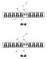
- FIG. 4Aschematically illustrates one side of an exemplary first PCB 30 compatible with the exemplary frame 20 schematically illustrated by FIG. 2 .
- the first PCB 30comprises a plurality of electrical contacts 36 along an edge 37 of the first PCB 30 .
- the plurality of electrical contacts 36are electrically coupled to a plurality of component contacts 38 which are connectable to the first plurality of components 34 .
- the plurality of electrical contacts 36 of the first PCB 30are electrically connectable to the third plurality of electrical contacts 72 of the first riser PCB 70 .
- the first PCB 30is configured to have components 34 only on one side, while in other embodiments, the first PCB 30 is configured to have components 34 on both sides.
- an exemplary second PCB 40comprises a plurality of electrical contacts 46 along an edge 47 of the second PCB 40 , with the plurality of electrical contacts 46 electrically coupled to a plurality of component contacts 48 which are connectable to the second plurality of components 44 .
- the plurality of electrical contacts 46 of the second PCB 40are electrically connectable to the fourth plurality of electrical contacts 82 of the second riser PCB 80 .
- the second PCB 40is configured to have components 44 only on one side, while in other embodiments, the second PCB 40 is configured to have components 44 on both sides.
- the first plurality of components 34 and/or the second plurality of components 44comprises integrated circuits having packaging which include but are not limited to, thin small-outline package (TSOP), ball-grid-array (BGA), fine-pitch BGA (FBGA), micro-BGA ( ⁇ BGA), mini-BGA (mBGA), and chip-scale packaging (CSP).
- TSOPthin small-outline package
- BGAball-grid-array
- FBGAfine-pitch BGA
- ⁇ BGAmicro-BGA
- mini-BGAmini-BGA
- CSPchip-scale packaging
- Memory components 34 , 44compatible with embodiments described herein, including but not limited to, random-access memory (RAM), dynamic random-access memory (DRAM), synchronous DRAM (SDRAM), and double-data-rate DRAM (e.g., DDR-1, DDR-2, DDR-3).
- DDR-1, DDR-2, DDR-3double-data-rate DRAM
- the component contacts 38 , 48are configured to be electrically connected to memory devices having BGA packaging.
- the components 34 , 44 of certain embodimentsfurther comprise other types of integrated circuits or electrical components, including, but not limited to, registers, clocks, and microprocessors.
- at least some of the components 34 of the first PCB 30are stacked (e.g., package stacked or die stacked) on one another, while in other embodiments, the components 34 of the first PCB 30 are not stacked on one another.
- at least some of the components 44 of the second PCB 40are stacked (e.g., package stacked or die stacked), while in other embodiments, the components 44 of the second PCB 40 are not stacked.
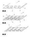
- FIG. 5schematically illustrates an exemplary module 10 with the exemplary frame 20 of FIG. 2 , a first PCB 30 with a first plurality of components 34 on a first surface 32 , and a second PCB 40 stacked with the first PCB 30 .
- the second PCB 40has a second plurality of components 44 on a second surface 42 facing the first surface 32 .
- the first PCB 30 and the second PCB 40are generally parallel to one another, while in other embodiments, the first PCB 30 and the second PCB 40 have a non-zero angle therebetween.
- the first PCB 30 of FIG. 5has component contacts 38 at the first surface 32 which are electrically connected to the corresponding components 34 and to the electrical contacts 36 at the end of the first PCB 30 .
- the electrical contacts 36 of the first PCB 30are electrically coupled to the electrical contacts 24 of the edge connector 22 through the electrical contacts 72 of the first riser PCB 70 , through the electrical contacts 62 of the base PCB 60 , and through the electrical conduits 68 of the base PCB 60 .
- the second PCB 40 of FIG. 5has component contacts 48 at the second surface 42 which are electrically connected to the corresponding components 44 and to the electrical contacts 46 at the end of the second PCB 40 . As schematically illustrated by FIG.
- the electrical contacts 46 of the second PCB 40are electrically coupled to the electrical contacts 24 of the edge connector 22 through the electrical contacts 82 of the second riser PCB 80 , through the electrical contacts 64 of the base PCB 60 , and through the electrical conduits 69 of the base PCB 60 .
- the first plurality of components 34are thermally coupled to the thermally conductive layer 50 a which is thermally coupled to a portion of the electrical contacts 24 of the edge connector 22 .
- the second plurality of components 44are thermally coupled to the thermally conductive layer 50 b which is thermally coupled to a portion of the electrical contacts 24 of the edge connector 22 .
- the thickness of the first riser PCB 70is selected to position the first surface 32 of the first PCB 30 at a desired distance from the thermally conductive layer 50 a .
- the thickness of the second riser PCB 80is selected to position the second surface 42 of the second PCB 40 at a desired distance from the thermally conductive layer 50 b .
- the at least one thermally conductive layer 50comprises a layer of a thermally conductive grease 50 c which contacts at least some of the components 34 , 44 and a corresponding one of the at least one thermally conductive layers 50 a , 50 b .
- the thermally conductive greaseprovides an improved thermal connection with the components 34 , 44 , thereby improving the heat transfer away from the components 34 , 44 .
- Persons skilled in the artcan select an appropriate thermally conductive grease 50 c in accordance with embodiments described herein.
- the module 10Upon connection of the exemplary module 10 schematically illustrated by FIG. 5 to a socket of a computer system motherboard, the module 10 provides a path for heat transfer from the first plurality of components 34 , through the thermally conductive grease 50 c and the thermally conductive layer 50 a , through the contacts 24 of the edge connector 22 , to the motherboard. Similarly, the module 10 provides a path for heat transfer from the second plurality of components 44 , through the thermally conductive grease 50 c and the thermally conductive layer 50 b , through the contacts 24 of the edge connector 22 , to the motherboard.
- certain embodimentsadvantageously do not utilize a separate thermal connection to other portions of the computer system (e.g., the chassis or enclosure) which may be inaccessible for this purpose.
- certain embodimentsadvantageously do not utilize separate heat spreaders on the outside surface of the module 10 which would otherwise increase the width of the module 10 .
- the at least one thermally conductive layer 50along with the electrical connections 24 of the edge connector 24 thereby serve as a heat spreader to dissipate heat from the components 34 , 44 .
- FIG. 6schematically illustrates an exemplary module 10 with the exemplary frame 20 of FIG. 2 , a first PCB 30 with a first plurality of components 34 on two surfaces, and a second PCB 40 with a second plurality of components 44 on two surfaces.
- the first PCB 30 of FIG. 6has component contacts 38 at both surfaces which are electrically connected to the corresponding components 34 and to the electrical contacts 36 at the end of the first PCB 30 .
- the components 34 on the first surface 32 of the first PCB 30are thermally coupled to the thermally conductive layer 50 a through a layer of thermally conductive grease 50 c .
- the components 34 on the opposite surface of the first PCB 30are not thermally coupled to the at least one thermally conductive layer 50 , while in other embodiments, the components 34 on the opposite surface of the first PCB 30 are thermally coupled to the at least one thermally conductive layer 50 .
- the second PCB 40 of FIG. 6has component contacts 48 at both surfaces which are electrically connected to the corresponding components 44 and to the electrical contacts 46 at the end of the first PCB 40 .
- the components 44 on the second surface 42 of the second PCB 40are thermally coupled to the thermally conductive layer 50 b through a layer of thermally conductive grease 50 c .
- the components 44 on the opposite surface of the second PCB 40are not thermally coupled to the at least one thermally conductive layer 50 , while in other embodiments, the components 44 on the opposite surface of the second PCB 40 are thermally coupled to the at least one thermally conductive layer 50 .
- Certain embodiments described hereinadvantageously provide stacked PCBs with improved thermal dissipation properties. Certain embodiments described herein advantageously provide memory modules with increased memory capacity while keeping the thickness of the memory module below a predetermined value. For example, for certain embodiments with components 34 , 44 comprising DDR2 DRAM integrated circuits with BGA packaging on both sides of each of the first PCB 30 and the second PCB 40 , the module 10 has a thickness of less than approximately 5.6 millimeters. Thus, certain embodiments advantageously allow use of the module 10 in cramped spaces. Certain embodiments advantageously reduce the cost of ventilation of the module 10 . Certain embodiments advantageously maintain temperatures of the components 34 , 44 within a desired operational temperature range.
- FIG. 7is a flowchart of an exemplary method 100 of fabricating a module 10 which is electrically connectable to a computer system in accordance with certain embodiments described herein. While the discussion of the method 100 herein refers to the structures schematically illustrated by FIGS. 2 , 5 , and 6 , persons skilled in the art recognize that other structures are also compatible with embodiments described herein.
- the method 100comprises providing a frame 20 comprising an edge connector 22 which is electrically connectable to the computer system.
- the frame 20further comprises at least one layer of thermally conductive material 50 which is thermally coupled to the edge connector 22 .
- the method 100further comprises mounting a first PCB 30 to the frame 20 .
- the first PCB 30has a first surface 32 and a first plurality of components 34 mounted thereon.
- the components 34are electrically coupled to the edge connector 22 and thermally coupled to the at least one layer of thermally conductive material 50 .
- the method 100further comprises mounting a second PCB 40 to the frame 20 .
- the second PCB 40has a second surface 42 and a second plurality of components 44 mounted thereon.
- the components 44are electrically coupled to the edge connector 22 and are thermally coupled to the at least one layer of thermally conductive material 50 .
- FIG. 8is a flowchart of providing the frame 20 in the operational block 110 in accordance with certain embodiments described herein.
- a base PCB 60is provided, wherein the base PCB 60 comprises the edge connector 22 , the at least one layer of thermally conductive material 50 , a plurality of electrical contacts 62 at a first surface 63 of the base PCB 60 , and a plurality of electrical contacts 64 at a second surface 65 of the base PCB 60 .
- the electrical contacts 62 , 64are electrically coupled to the edge connector 22 .
- a first riser PCB 70comprising a plurality of electrical contacts 72 is coupled to the base PCB 60 .
- coupling the first riser PCB 70 to the base PCB 60comprises electrically coupling the electrical contacts 72 of the first riser PCB 70 to the plurality of electrical contacts 62 at the first surface 63 of the base PCB 60 .
- a second riser PCB 80 comprising a plurality of electrical contacts 82is coupled to the base PCB 60 .
- coupling the second riser PCB 80 to the base PCB 60comprises electrically coupling the electrical contacts 82 of the second riser PCB 80 to the plurality of electrical contacts 64 at the second surface 65 of the base PCB 60 .
- FIG. 9is a flowchart of mounting the first PCB 30 to the frame 20 in the operational block 120 in accordance with certain embodiments described herein.
- the first PCB 30is provided, wherein the first PCB 30 comprises a plurality of components 34 , a plurality of electrical contacts 36 along an edge 37 of the first PCB 30 , and a plurality of component contacts 38 .
- the electrical contacts 36are electrically coupled to the components 34 through the component contacts 38 .
- the electrical contacts 36are electrically coupled to the electrical contacts 72 of the first riser PCB 70 .
- FIG. 10is a flowchart of mounting the second PCB 40 to the frame 20 in the operational block 130 in accordance with certain embodiments described herein.
- the second PCB 40is provided, wherein the second PCB 40 comprises a plurality of components 44 , a plurality of electrical contacts 46 along an edge 47 of the second PCB 40 , and a plurality of component contacts 48 .
- the electrical contacts 46are electrically coupled to the components 44 through the component contacts 48 .
- the electrical contacts 46are electrically coupled to the electrical contacts 82 of the second riser PCB 80 .
- each PCB used to fabricate the module 10has fiducial marks or structures which fit into a jig or other framework to facilitate orienting the PCBs relative to one another during fabrication.
- structures compatible with embodiments described hereininclude, but are not limited to, notches, ridges, pins, and holes.
- FIGS. 11A-11Cschematically illustrate exemplary PCBs with holes 150 which fit onto corresponding pins of a jig (not shown).
- FIG. 11Aschematically illustrates a first PCB 30 with a plurality of holes 150 at selected positions.
- FIG. 11Bschematically illustrates a first riser PCB 70 with a plurality of holes 150 at corresponding positions.
- FIG. 11Cschematically illustrates a base PCB 60 with a plurality of holes 150 at corresponding positions.
- each of the second PCB 40 and the second riser PCB 80 of certain embodimentshas a plurality of holes 150 at corresponding positions.
- Other embodimentshave different numbers of holes 150 at different positions than those schematically illustrated by FIGS. 11A-11C . Persons skilled in the art can select appropriate hole sizes and positions in accordance with embodiments described herein.
- FIG. 12is a flowchart of an exemplary fabrication method 200 using a jig having pins corresponding to the holes 150 of the PCBs schematically illustrated by FIGS. 11A-11C .
- the first PCB 30is placed on the jig with the pins extending through the holes 150 of the first PCB 30 .
- the first PCB 30is placed on the jig with the first surface 32 facing upwards.
- the first riser PCB 70is placed on the jig with the pins extending through the holes 150 of the first riser PCB 70 .
- the electrical contacts 72 of the first riser PCB 70are proximal to the electrical contacts 36 of the first PCB 30 .
- the base PCB 60is placed on the jig with the pins extending through the holes 150 of the base PCB 60 .
- the electrical contacts 62 of the base PCB 60are proximal to the electrical contacts 72 of the first riser PCB 70 .
- the at least one thermally conductive layer 50is thermally coupled to the components 34 of the first PCB 30 .
- a thermally conductive greaseis applied between the components 34 of the first PCB 30 and the at least one thermally conductive layer 50 prior to placing the base PCB 60 and the first PCB 30 together.
- the thermally conductive grease of certain embodimentsadvantageously facilitates thermal coupling between the components 34 and the at least one thermally conductive layer 50 of the frame 20 .
- the second riser PCB 80is placed on the jig with the pins extending through the holes 150 of the second riser PCB 80 .
- the electrical contacts 82 of the second riser PCB 80are proximal to the electrical contacts 64 of the base PCB 60 .
- the second PCB 40is placed on the jig with the pins extending through the holes 150 of the second PCB 40 .
- the electrical contacts 46 of the second PCB 40are proximal to the electrical contacts 82 of the second riser PCB 80 .
- the second PCB 40is placed on the jig with the second surface 42 facing downwards.
- the at least one thermally conductive layer 50is thermally coupled to the components 44 of the second PCB 40 .
- a thermally conductive greaseis applied between the top components 44 of the second PCB 40 and the at least one thermally conductive layer 50 prior to placing the base PCB 60 and the second PCB 40 together.
- the thermally conductive grease of certain embodimentsadvantageously facilitates thermal coupling between the components 44 and the at least one thermally conductive layer 50 of the frame 20 .
- the electrical contacts of the various PCBsare electrically coupled together to provide electrical conductivity between the edge connector 22 and the components 34 , 44 .
- the electrical contacts 36 of the first PCB 30are electrically coupled to the electrical contacts 72 of the first riser PCB 70 .
- the electrical contacts 72 of the first riser PCB 70are electrically coupled to the electrical contacts 62 of the base PCB 60 .
- the electrical contacts 64 of the base PCB 60are electrically coupled to the electrical contacts 82 of the second riser PCB 80 .
- the electrical contacts 82 of the second riser PCB 80are electrically coupled to the electrical contacts 46 of the second PCB 40 .
- Examples of methods of electrically coupling the respective electrical contactsinclude, but are not limited to, edge-bonded interconnects (as described more fully below), through-hole interconnects, male-female connections, J-clips, and flex circuitry. Persons skilled in the art can select appropriate methods of electrically coupling the respective electrical contacts in accordance with embodiments described herein.
- through-hole interconnectssuffer from various problems.
- solder joints used to provide the interconnectionare located between the two PCBs, so the solder joints are not visible and are not accessible for visual inspection.
- the through-hole interconnectsadd to the cost of manufacturing the module 10 .
- the through-hole interconnectsdo not provide reliable electrical interconnections between the two PCBs.
- each of the first riser PCB 70 and the second riser PCB 80has plated contacts in proximity to an edge of the PCB (e.g., either on the edge or cut into the edge, as schematically illustrated by FIG. 3C ).
- each of the operational blocks 262 , 264 , 266 , 268are performed by applying solder to the plated contacts and reflowing the solder using localized heating.
- localized heatingcertain such embodiments advantageously avoid exposing the components 34 , 44 to additional heat cycling, thereby reducing the probability of degradation or failure of the components 34 , 44 .
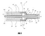
- FIG. 13schematically illustrates a side view of exemplary electrical connections between the electrical contacts 62 of the base PCB 60 , the electrical contacts 72 of the first riser PCB 70 , and the electrical contacts 36 of the first PCB 30 using edge-bonded interconnects.
- the plated electrical contacts 62 , 72 , 36 in proximity to the edge of the PCBsare wetted by the solder 160 , as schematically illustrated by FIG. 13 .
- the edge-bonded interconnects of certain embodimentsprovide vertical connections between two PCBs.
- applying the solder 160 to the outside surfaces of the electrical contacts 62 , 72 , 36advantageously permits visual inspection of the resultant electrical connections, thereby avoiding techniques such as x-ray analysis.
- the electrical connections between the electrical contacts 62 of the base PCB 60 and the electrical contacts 36 of the first PCB 30are advantageously facilitated in certain embodiments by the form of the electrical contacts 72 of the first riser PCB 70 , as schematically illustrated by FIG. 3C .
- Such structures for the electrical contacts 72provide recesses into which the solder 160 advantageously reflows upon localized heating.
- the edge-bonded interconnectsadvantageously simplify the module and board design, and reduce the cost of manufacturing the module and the board. By providing interconnects which can be visually inspected, certain embodiments utilizing edge-bonded interconnects advantageously facilitate identification of poor interconnections which can be rejected or reworked.
- the at least one thermally conductive layer 50comprises two thermally conductive layers 50 a , 50 b on either side of a dielectric layer 61 .
- FIGS. 2 , 5 , and 6schematically illustrate such embodiments.
- the two thermally conductive layers 50 a , 50 bare also electrically conductive
- the two thermally conductive layers 50 a , 50 bare thermally and electrically coupled to the same electrical contacts 22 of the edge connector 24 .
- the two thermally conductive layers 50 a , 50 bare thermally and electrically coupled to two separate sets of the electrical contacts 22 of the edge connector 24 .
- the two thermally conductive layers 50 a , 50 bare electrically isolated from one another.
- one thermally conductive layer 50 ais thermally and electrically coupled to the electrical contacts 22 corresponding to a ground plane while the other thermally conductive layer 50 b is thermally and electrically coupled to the electrical contacts 22 corresponding to a voltage plane.
- the frame 20comprises between approximately twenty to thirty electrical contacts 22 to ground and between approximately twenty to thirty electrical contacts 22 to a power voltage.
- the number of electrical contacts 22 used to provide the thermal pathis advantageously increased by connecting the thermally conductive layers 50 a , 50 b to different sets of electrical contacts 22 .
- Certain such embodimentsadvantageously provide a degree of electromagnetic interference (EMI) shielding of the components 34 , 44 of the module 10 .
- Certain other such embodimentsadvantageously provide capacitance between the two thermally conductive layers 50 a , 50 b which facilitates noise reduction of the voltage applied to the voltage plane.
- EMIelectromagnetic interference
- the module 10further comprises a thermally conductive piece 170 which is positioned on the module 10 along a portion of the opposite edge away from the edge connector 22 , as schematically illustrated by FIG. 14 .
- the piece 170is thermally coupled to the at least one thermally conductive layer 50 and provides a second thermal path for heat to transfer to the piece 170 from the components 34 , 44 , through the at least one thermally conductive layer 50 . The heat can then be dissipated away from the piece 170 by convection to the environment surrounding the module 10 .
- FIG. 15schematically illustrates an exemplary module 10 having a first frame portion 180 and a second frame portion 182 in accordance with embodiments described herein.
- the at least one thermally conductive layer 50extends from the first portion 180 of the frame 20 to the second portion 182 of the frame 20 .
- Each of the first PCB 30 and the second PCB 40is coupled to both the first portion 180 of the frame 20 and the second portion 182 of the frame 20 (e.g., by solder balls 184 ).
- the at least one thermally conductive layer 50is sandwiched between the components 34 of the first PCB 30 and the components 44 of the second PCB 40 .
Landscapes
- Engineering & Computer Science (AREA)
- Microelectronics & Electronic Packaging (AREA)
- Cooling Or The Like Of Electrical Apparatus (AREA)
Abstract
Description
Claims (32)
Priority Applications (2)
| Application Number | Priority Date | Filing Date | Title |
|---|---|---|---|
| US12/939,915US8345427B2 (en) | 2004-04-09 | 2010-11-04 | Module having at least two surfaces and at least one thermally conductive layer therebetween |
| US13/731,014US8971045B1 (en) | 2004-04-09 | 2012-12-30 | Module having at least one thermally conductive layer between printed circuit boards |
Applications Claiming Priority (7)
| Application Number | Priority Date | Filing Date | Title |
|---|---|---|---|
| US56100904P | 2004-04-09 | 2004-04-09 | |
| US58977704P | 2004-07-21 | 2004-07-21 | |
| US11/101,155US7254036B2 (en) | 2004-04-09 | 2005-04-07 | High density memory module using stacked printed circuit boards |
| US11/775,125US7375970B2 (en) | 2004-04-09 | 2007-07-09 | High density memory module using stacked printed circuit boards |
| US12/052,678US7630202B2 (en) | 2004-04-09 | 2008-03-20 | High density module having at least two substrates and at least one thermally conductive layer therebetween |
| US12/606,136US7839645B2 (en) | 2004-04-09 | 2009-10-26 | Module having at least two surfaces and at least one thermally conductive layer therebetween |
| US12/939,915US8345427B2 (en) | 2004-04-09 | 2010-11-04 | Module having at least two surfaces and at least one thermally conductive layer therebetween |
Related Parent Applications (1)
| Application Number | Title | Priority Date | Filing Date |
|---|---|---|---|
| US12/606,136ContinuationUS7839645B2 (en) | 2004-04-09 | 2009-10-26 | Module having at least two surfaces and at least one thermally conductive layer therebetween |
Related Child Applications (1)
| Application Number | Title | Priority Date | Filing Date |
|---|---|---|---|
| US13/731,014ContinuationUS8971045B1 (en) | 2004-04-09 | 2012-12-30 | Module having at least one thermally conductive layer between printed circuit boards |
Publications (2)
| Publication Number | Publication Date |
|---|---|
| US20110110047A1 US20110110047A1 (en) | 2011-05-12 |
| US8345427B2true US8345427B2 (en) | 2013-01-01 |
Family
ID=35942729
Family Applications (6)
| Application Number | Title | Priority Date | Filing Date |
|---|---|---|---|
| US11/101,155Active2025-10-29US7254036B2 (en) | 2004-04-09 | 2005-04-07 | High density memory module using stacked printed circuit boards |
| US11/775,125Expired - Fee RelatedUS7375970B2 (en) | 2004-04-09 | 2007-07-09 | High density memory module using stacked printed circuit boards |
| US12/052,678Expired - LifetimeUS7630202B2 (en) | 2004-04-09 | 2008-03-20 | High density module having at least two substrates and at least one thermally conductive layer therebetween |
| US12/606,136Expired - LifetimeUS7839645B2 (en) | 2004-04-09 | 2009-10-26 | Module having at least two surfaces and at least one thermally conductive layer therebetween |
| US12/939,915Expired - LifetimeUS8345427B2 (en) | 2004-04-09 | 2010-11-04 | Module having at least two surfaces and at least one thermally conductive layer therebetween |
| US13/731,014Expired - LifetimeUS8971045B1 (en) | 2004-04-09 | 2012-12-30 | Module having at least one thermally conductive layer between printed circuit boards |
Family Applications Before (4)
| Application Number | Title | Priority Date | Filing Date |
|---|---|---|---|
| US11/101,155Active2025-10-29US7254036B2 (en) | 2004-04-09 | 2005-04-07 | High density memory module using stacked printed circuit boards |
| US11/775,125Expired - Fee RelatedUS7375970B2 (en) | 2004-04-09 | 2007-07-09 | High density memory module using stacked printed circuit boards |
| US12/052,678Expired - LifetimeUS7630202B2 (en) | 2004-04-09 | 2008-03-20 | High density module having at least two substrates and at least one thermally conductive layer therebetween |
| US12/606,136Expired - LifetimeUS7839645B2 (en) | 2004-04-09 | 2009-10-26 | Module having at least two surfaces and at least one thermally conductive layer therebetween |
Family Applications After (1)
| Application Number | Title | Priority Date | Filing Date |
|---|---|---|---|
| US13/731,014Expired - LifetimeUS8971045B1 (en) | 2004-04-09 | 2012-12-30 | Module having at least one thermally conductive layer between printed circuit boards |
Country Status (1)
| Country | Link |
|---|---|
| US (6) | US7254036B2 (en) |
Cited By (7)
| Publication number | Priority date | Publication date | Assignee | Title |
|---|---|---|---|---|
| US8930647B1 (en) | 2011-04-06 | 2015-01-06 | P4tents1, LLC | Multiple class memory systems |
| US9158546B1 (en) | 2011-04-06 | 2015-10-13 | P4tents1, LLC | Computer program product for fetching from a first physical memory between an execution of a plurality of threads associated with a second physical memory |
| US9164679B2 (en) | 2011-04-06 | 2015-10-20 | Patents1, Llc | System, method and computer program product for multi-thread operation involving first memory of a first memory class and second memory of a second memory class |
| US9170744B1 (en) | 2011-04-06 | 2015-10-27 | P4tents1, LLC | Computer program product for controlling a flash/DRAM/embedded DRAM-equipped system |
| US9176671B1 (en) | 2011-04-06 | 2015-11-03 | P4tents1, LLC | Fetching data between thread execution in a flash/DRAM/embedded DRAM-equipped system |
| US9417754B2 (en) | 2011-08-05 | 2016-08-16 | P4tents1, LLC | User interface system, method, and computer program product |
| US12094803B2 (en) | 2021-04-21 | 2024-09-17 | Samsung Electronics Co., Ltd. | Solid state drive apparatus and data storage apparatus including the same |
Families Citing this family (73)
| Publication number | Priority date | Publication date | Assignee | Title |
|---|---|---|---|---|
| US20070164424A1 (en)* | 2003-04-02 | 2007-07-19 | Nancy Dean | Thermal interconnect and interface systems, methods of production and uses thereof |
| JP2007527105A (en)* | 2003-06-06 | 2007-09-20 | ハネウエル・インターナシヨナル・インコーポレーテツド | Thermal coupling system and manufacturing method thereof |
| KR20050022798A (en)* | 2003-08-30 | 2005-03-08 | 주식회사 이즈텍 | A system for analyzing bio chips using gene ontology, and a method thereof |
| US7916574B1 (en) | 2004-03-05 | 2011-03-29 | Netlist, Inc. | Circuit providing load isolation and memory domain translation for memory module |
| US7254036B2 (en)* | 2004-04-09 | 2007-08-07 | Netlist, Inc. | High density memory module using stacked printed circuit boards |
| US7616452B2 (en)* | 2004-09-03 | 2009-11-10 | Entorian Technologies, Lp | Flex circuit constructions for high capacity circuit module systems and methods |
| US7606049B2 (en)* | 2004-09-03 | 2009-10-20 | Entorian Technologies, Lp | Module thermal management system and method |
| US7443023B2 (en)* | 2004-09-03 | 2008-10-28 | Entorian Technologies, Lp | High capacity thin module system |
| US20060109631A1 (en)* | 2004-11-02 | 2006-05-25 | Data Device Corporation | Method and apparatus for connecting circuit cards employing a cooling technique to achieve desired temperature thresholds and card alignment |
| US8386722B1 (en) | 2008-06-23 | 2013-02-26 | Google Inc. | Stacked DIMM memory interface |
| US8060774B2 (en) | 2005-06-24 | 2011-11-15 | Google Inc. | Memory systems and memory modules |
| US8335894B1 (en) | 2008-07-25 | 2012-12-18 | Google Inc. | Configurable memory system with interface circuit |
| US8130560B1 (en) | 2006-11-13 | 2012-03-06 | Google Inc. | Multi-rank partial width memory modules |
| US10013371B2 (en) | 2005-06-24 | 2018-07-03 | Google Llc | Configurable memory circuit system and method |
| US7609567B2 (en) | 2005-06-24 | 2009-10-27 | Metaram, Inc. | System and method for simulating an aspect of a memory circuit |
| US8055833B2 (en) | 2006-10-05 | 2011-11-08 | Google Inc. | System and method for increasing capacity, performance, and flexibility of flash storage |
| US9507739B2 (en) | 2005-06-24 | 2016-11-29 | Google Inc. | Configurable memory circuit system and method |
| US8796830B1 (en) | 2006-09-01 | 2014-08-05 | Google Inc. | Stackable low-profile lead frame package |
| US8438328B2 (en) | 2008-02-21 | 2013-05-07 | Google Inc. | Emulation of abstracted DIMMs using abstracted DRAMs |
| US8359187B2 (en) | 2005-06-24 | 2013-01-22 | Google Inc. | Simulating a different number of memory circuit devices |
| US8244971B2 (en) | 2006-07-31 | 2012-08-14 | Google Inc. | Memory circuit system and method |
| US9171585B2 (en) | 2005-06-24 | 2015-10-27 | Google Inc. | Configurable memory circuit system and method |
| US9542352B2 (en) | 2006-02-09 | 2017-01-10 | Google Inc. | System and method for reducing command scheduling constraints of memory circuits |
| US7386656B2 (en) | 2006-07-31 | 2008-06-10 | Metaram, Inc. | Interface circuit system and method for performing power management operations in conjunction with only a portion of a memory circuit |
| US8327104B2 (en) | 2006-07-31 | 2012-12-04 | Google Inc. | Adjusting the timing of signals associated with a memory system |
| US20080028136A1 (en) | 2006-07-31 | 2008-01-31 | Schakel Keith R | Method and apparatus for refresh management of memory modules |
| US8081474B1 (en) | 2007-12-18 | 2011-12-20 | Google Inc. | Embossed heat spreader |
| US8111566B1 (en) | 2007-11-16 | 2012-02-07 | Google, Inc. | Optimal channel design for memory devices for providing a high-speed memory interface |
| US8041881B2 (en) | 2006-07-31 | 2011-10-18 | Google Inc. | Memory device with emulated characteristics |
| US8090897B2 (en) | 2006-07-31 | 2012-01-03 | Google Inc. | System and method for simulating an aspect of a memory circuit |
| US8397013B1 (en) | 2006-10-05 | 2013-03-12 | Google Inc. | Hybrid memory module |
| US8077535B2 (en) | 2006-07-31 | 2011-12-13 | Google Inc. | Memory refresh apparatus and method |
| US20080082763A1 (en) | 2006-10-02 | 2008-04-03 | Metaram, Inc. | Apparatus and method for power management of memory circuits by a system or component thereof |
| US8089795B2 (en) | 2006-02-09 | 2012-01-03 | Google Inc. | Memory module with memory stack and interface with enhanced capabilities |
| US7392338B2 (en) | 2006-07-31 | 2008-06-24 | Metaram, Inc. | Interface circuit system and method for autonomously performing power management operations in conjunction with a plurality of memory circuits |
| US7442050B1 (en) | 2005-08-29 | 2008-10-28 | Netlist, Inc. | Circuit card with flexible connection for memory module with heat spreader |
| WO2007028109A2 (en) | 2005-09-02 | 2007-03-08 | Metaram, Inc. | Methods and apparatus of stacking drams |
| US9632929B2 (en) | 2006-02-09 | 2017-04-25 | Google Inc. | Translating an address associated with a command communicated between a system and memory circuits |
| US7619893B1 (en) | 2006-02-17 | 2009-11-17 | Netlist, Inc. | Heat spreader for electronic modules |
| DE102006018874A1 (en)* | 2006-04-24 | 2007-10-25 | Infineon Technologies Ag | Circuit arrangement for coupling a voltage supply to a semiconductor component, method for producing the circuit arrangement and data processing apparatus comprising the circuit arrangement |
| WO2007142273A1 (en)* | 2006-06-08 | 2007-12-13 | International Business Machines Corporation | Highly heat conductive, flexible sheet |
| US7724589B2 (en) | 2006-07-31 | 2010-05-25 | Google Inc. | System and method for delaying a signal communicated from a system to at least one of a plurality of memory circuits |
| US7539024B1 (en)* | 2006-08-02 | 2009-05-26 | Chris Karabatsos | Active dual in line memory module connector with re-driven propagated signals |
| US8040683B2 (en)* | 2006-08-02 | 2011-10-18 | Urenschi Assets Limited Liability Company | Active dual in line memory module connector with re-driven propagated signals |
| US7615860B2 (en)* | 2007-04-19 | 2009-11-10 | Advanced Flexible Circuits Co., Ltd. | Rigid-flex printed circuit board with weakening structure |
| US8209479B2 (en) | 2007-07-18 | 2012-06-26 | Google Inc. | Memory circuit system and method |
| US8080874B1 (en) | 2007-09-14 | 2011-12-20 | Google Inc. | Providing additional space between an integrated circuit and a circuit board for positioning a component therebetween |
| JP4450070B2 (en)* | 2007-12-28 | 2010-04-14 | ソニー株式会社 | Electronics |
| US8198710B2 (en) | 2008-02-05 | 2012-06-12 | Fairchild Semiconductor Corporation | Folded leadframe multiple die package |
| US8154901B1 (en) | 2008-04-14 | 2012-04-10 | Netlist, Inc. | Circuit providing load isolation and noise reduction |
| US8787060B2 (en) | 2010-11-03 | 2014-07-22 | Netlist, Inc. | Method and apparatus for optimizing driver load in a memory package |
| US8018723B1 (en) | 2008-04-30 | 2011-09-13 | Netlist, Inc. | Heat dissipation for electronic modules |
| DE202010017690U1 (en) | 2009-06-09 | 2012-05-29 | Google, Inc. | Programming dimming terminating resistor values |
| US9128632B2 (en) | 2009-07-16 | 2015-09-08 | Netlist, Inc. | Memory module with distributed data buffers and method of operation |
| CN103650655B (en)* | 2011-06-28 | 2018-04-13 | 爱立信(中国)通信有限公司 | Electronic equipment with heat dissipation structure |
| US20130318269A1 (en) | 2012-05-22 | 2013-11-28 | Xockets IP, LLC | Processing structured and unstructured data using offload processors |
| US20130318084A1 (en) | 2012-05-22 | 2013-11-28 | Xockets IP, LLC | Processing structured and unstructured data using offload processors |
| US9378161B1 (en) | 2013-01-17 | 2016-06-28 | Xockets, Inc. | Full bandwidth packet handling with server systems including offload processors |
| US9250954B2 (en) | 2013-01-17 | 2016-02-02 | Xockets, Inc. | Offload processor modules for connection to system memory, and corresponding methods and systems |
| US10324841B2 (en) | 2013-07-27 | 2019-06-18 | Netlist, Inc. | Memory module with local synchronization |
| US20160105984A1 (en)* | 2014-10-09 | 2016-04-14 | International Rectifier Corporation | Power Unit with Conductive Slats |
| JP6601055B2 (en)* | 2015-08-20 | 2019-11-06 | 富士通株式会社 | Printed wiring board, electronic device and mounting method |
| US10098241B2 (en)* | 2015-10-23 | 2018-10-09 | International Business Machines Corporation | Printed circuit board with edge soldering for high-density packages and assemblies |
| KR102449193B1 (en) | 2015-12-04 | 2022-09-29 | 삼성전자주식회사 | Memory package including buffer, expandable memory module and multi-module memory system |
| US20170325327A1 (en)* | 2016-04-07 | 2017-11-09 | Massachusetts Institute Of Technology | Printed circuit board for high power components |
| US10679722B2 (en) | 2016-08-26 | 2020-06-09 | Sandisk Technologies Llc | Storage system with several integrated components and method for use therewith |
| US10312174B2 (en)* | 2016-08-29 | 2019-06-04 | Apple Inc. | Thermal management system |
| US10193248B2 (en) | 2016-08-31 | 2019-01-29 | Crystal Group, Inc. | System and method for retaining memory modules |
| US10199904B2 (en) | 2017-02-23 | 2019-02-05 | Schaft Inc. | Cooling a heat-generating electronic device |
| US10488898B2 (en)* | 2017-03-31 | 2019-11-26 | Microsoft Technology Licensing, Llc | Flexible heat spreader |
| US10734756B2 (en) | 2018-08-10 | 2020-08-04 | Crystal Group Inc. | DIMM/expansion card retention method for highly kinematic environments |
| JP7144732B2 (en)* | 2018-09-19 | 2022-09-30 | 株式会社デンソーウェーブ | laminated substrate |
| US11121504B2 (en)* | 2020-02-03 | 2021-09-14 | Rockwell Collins, Inc. | Circuit board separation mechanism |
Citations (115)
| Publication number | Priority date | Publication date | Assignee | Title |
|---|---|---|---|---|
| US3268772A (en) | 1963-03-26 | 1966-08-23 | North American Aviation Inc | Packaged electronic equipment |
| US3893161A (en) | 1974-02-04 | 1975-07-01 | Jr Albert Pesak | Frictionally engageable heat sink for solid state devices |
| US4535385A (en) | 1983-04-22 | 1985-08-13 | Cray Research, Inc. | Circuit module with enhanced heat transfer and distribution |
| US4628407A (en) | 1983-04-22 | 1986-12-09 | Cray Research, Inc. | Circuit module with enhanced heat transfer and distribution |
| US4849858A (en) | 1986-10-20 | 1989-07-18 | Westinghouse Electric Corp. | Composite heat transfer means |
| US4867235A (en) | 1986-10-20 | 1989-09-19 | Westinghouse Electric Corp. | Composite heat transfer means |
| US4872505A (en) | 1988-08-16 | 1989-10-10 | Ncr Corporation | Heat sink for an electronic device |
| US4887353A (en) | 1985-05-01 | 1989-12-19 | Amp Incorporated | Conduction cooled module connector system and method of making |
| US5060113A (en) | 1987-04-09 | 1991-10-22 | Raychem Corporation | Connector assembly |
| US5109318A (en) | 1990-05-07 | 1992-04-28 | International Business Machines Corporation | Pluggable electronic circuit package assembly with snap together heat sink housing |
| US5229916A (en) | 1992-03-04 | 1993-07-20 | International Business Machines Corporation | Chip edge interconnect overlay element |
| US5244023A (en) | 1991-09-11 | 1993-09-14 | Spies Albert L | Device for securing articles on or about the person |
| US5313097A (en) | 1992-11-16 | 1994-05-17 | International Business Machines, Corp. | High density memory module |
| US5343359A (en) | 1992-11-19 | 1994-08-30 | Cray Research, Inc. | Apparatus for cooling daughter boards |
| US5432913A (en) | 1990-09-21 | 1995-07-11 | Smits; Gerard D. | Computer system module |
| US5445869A (en) | 1993-01-21 | 1995-08-29 | Matsushita Electric Industrial Co., Ltd. | Composite flexible substrate |
| US5513135A (en) | 1994-12-02 | 1996-04-30 | International Business Machines Corporation | Synchronous memory packaged in single/dual in-line memory module and method of fabrication |
| US5731633A (en) | 1992-09-16 | 1998-03-24 | Gary W. Hamilton | Thin multichip module |
| US5739687A (en) | 1995-11-15 | 1998-04-14 | Oxford Instruments (Uk) Limited | Magnetic field generating assembly |
| US5754409A (en) | 1996-11-06 | 1998-05-19 | Dynamem, Inc. | Foldable electronic assembly module |
| US5784263A (en) | 1996-01-08 | 1998-07-21 | Intel Corporation | Connector with attachable daughter card retention system |
| US5812374A (en) | 1996-10-28 | 1998-09-22 | Shuff; Gregg Douglas | Electrical circuit cooling device |
| JP2821315B2 (en) | 1992-06-02 | 1998-11-05 | 日本電気株式会社 | Single inline module |
| US5892658A (en) | 1998-05-12 | 1999-04-06 | Lockhead Martin Corporation | VME eurocard triple printed wiring board single slot module assembly |
| US5901781A (en) | 1996-02-17 | 1999-05-11 | Arai; Seihachi | Heat radiator for electronic parts |
| US5949650A (en) | 1998-09-02 | 1999-09-07 | Hughes Electronics Corporation | Composite heat sink/support structure |
| US5949657A (en) | 1997-12-01 | 1999-09-07 | Karabatsos; Chris | Bottom or top jumpered foldable electronic assembly |
| US5966287A (en) | 1997-12-17 | 1999-10-12 | Intel Corporation | Clip on heat exchanger for a memory module and assembly method |
| US5986887A (en) | 1998-10-28 | 1999-11-16 | Unisys Corporation | Stacked circuit board assembly adapted for heat dissipation |
| US6002585A (en)* | 1997-06-03 | 1999-12-14 | Telefonaktiebolaget Lm Ericsson | Device and method for cooling and protecting electronics |
| US6021048A (en) | 1998-02-17 | 2000-02-01 | Smith; Gary W. | High speed memory module |
| US6025992A (en) | 1999-02-11 | 2000-02-15 | International Business Machines Corp. | Integrated heat exchanger for memory module |
| US6064575A (en) | 1998-05-12 | 2000-05-16 | Lockheed Martin Corporation | Circuit module assembly |
| US6151215A (en) | 1998-12-08 | 2000-11-21 | Alliedsignal Inc. | Single mount and cooling for two two-sided printed circuit boards |
| US6157541A (en) | 1997-12-30 | 2000-12-05 | Siemens Aktiengesellschaft | Stack arrangement for two semiconductor memory chips and printed board for accepting a plurality of such stack arrangements |
| US6173382B1 (en) | 1998-04-28 | 2001-01-09 | International Business Machines Corporation | Dynamic configuration of memory module using modified presence detect data |
| US6180881B1 (en) | 1998-05-05 | 2001-01-30 | Harlan Ruben Isaak | Chip stack and method of making same |
| US6201700B1 (en) | 2000-01-06 | 2001-03-13 | Ford Motor Company | Box design for maximum heat dissipation |
| JP2001077294A (en) | 1999-09-02 | 2001-03-23 | Nec Corp | Semiconductor device |
| US6208517B1 (en) | 1999-09-10 | 2001-03-27 | Legerity, Inc. | Heat sink |
| US6222739B1 (en) | 1998-01-20 | 2001-04-24 | Viking Components | High-density computer module with stacked parallel-plane packaging |
| US6297960B1 (en) | 1998-06-30 | 2001-10-02 | Micron Technology, Inc. | Heat sink with alignment and retaining features |
| US6381140B1 (en) | 1999-08-30 | 2002-04-30 | Witek Enterprise Co., Ltd. | Memory module |
| US6392305B1 (en) | 1999-03-31 | 2002-05-21 | Chih-Kung Huang | Chip scale package of semiconductor |
| US20020076959A1 (en) | 2000-12-20 | 2002-06-20 | George Lee | Card edge connector with safety ejector |
| US6423909B1 (en) | 2001-02-27 | 2002-07-23 | Hewlett-Packard Company | Circuit board construction for differential bus distribution |
| US6424532B2 (en) | 1998-06-12 | 2002-07-23 | Nec Corporation | Heat sink and memory module with heat sink |
| US6444921B1 (en) | 2000-02-03 | 2002-09-03 | Fujitsu Limited | Reduced stress and zero stress interposers for integrated-circuit chips, multichip substrates, and the like |
| US6449159B1 (en) | 2000-05-03 | 2002-09-10 | Rambus Inc. | Semiconductor module with imbedded heat spreader |
| US20020125039A1 (en) | 1999-05-25 | 2002-09-12 | Marketkar Nandu J. | Electromagnetic coupler alignment |
| US6507912B1 (en) | 1999-01-27 | 2003-01-14 | International Business Machines Corporation | Protection of biometric data via key-dependent sampling |
| US6510100B2 (en) | 2000-12-04 | 2003-01-21 | International Business Machines Corporation | Synchronous memory modules and memory systems with selectable clock termination |
| US6535387B2 (en) | 2001-06-28 | 2003-03-18 | Intel Corporation | Heat transfer apparatus |
| JP2003086760A (en) | 2001-09-12 | 2003-03-20 | Hitachi Ltd | Semiconductor device and method of manufacturing the same |
| JP2003086761A (en) | 2001-09-14 | 2003-03-20 | Casio Comput Co Ltd | Semiconductor device and manufacturing method thereof |
| US6576992B1 (en) | 2001-10-26 | 2003-06-10 | Staktek Group L.P. | Chip scale stacking system and method |
| US20030116835A1 (en) | 1999-02-26 | 2003-06-26 | Hitachi, Ltd. | Memory-module and a method of manufacturing the same |
| US6590282B1 (en) | 2002-04-12 | 2003-07-08 | Industrial Technology Research Institute | Stacked semiconductor package formed on a substrate and method for fabrication |
| US6665190B2 (en)* | 1992-09-16 | 2003-12-16 | James E. Clayton | Modular PC card which receives add-in PC card modules |
| US20030234443A1 (en) | 2001-10-26 | 2003-12-25 | Staktek Group, L.P. | Low profile stacking system and method |
| US6713854B1 (en) | 2000-10-16 | 2004-03-30 | Legacy Electronics, Inc | Electronic circuit module with a carrier having a mounting pad array |
| US6740821B1 (en) | 2002-03-01 | 2004-05-25 | Micron Technology, Inc. | Selectively configurable circuit board |
| US6757751B1 (en) | 2000-08-11 | 2004-06-29 | Harrison Gene | High-speed, multiple-bank, stacked, and PCB-mounted memory module |
| US6762942B1 (en) | 2002-09-05 | 2004-07-13 | Gary W. Smith | Break away, high speed, folded, jumperless electronic assembly |
| US20040218360A1 (en) | 2003-05-02 | 2004-11-04 | Delta Electronics, Inc. | Heat-dispersing fan module of electronic apparatus |
| US20040229402A1 (en) | 2001-10-26 | 2004-11-18 | Staktek Group, L.P. | Low profile chip scale stacking system and method |
| US20040236877A1 (en) | 1997-12-17 | 2004-11-25 | Lee A. Burton | Switch/network adapter port incorporating shared memory resources selectively accessible by a direct execution logic element and one or more dense logic devices in a fully buffered dual in-line memory module format (FB-DIMM) |
| US6833984B1 (en) | 2000-05-03 | 2004-12-21 | Rambus, Inc. | Semiconductor module with serial bus connection to multiple dies |
| US20040262737A1 (en) | 2000-05-03 | 2004-12-30 | Belgacem Haba | Semiconductor module |
| US20050018412A1 (en) | 2001-10-26 | 2005-01-27 | Staktek Group, L.P. | Pitch change and chip scale stacking system |
| US20050047776A1 (en) | 2002-04-18 | 2005-03-03 | Olympus Optical Co., Ltd. | Camera |
| US20050057911A1 (en) | 2003-09-15 | 2005-03-17 | Staktek Group, L.P. | Memory expansion and integrated circuit stacking system and method |
| US20050078457A1 (en) | 2003-10-09 | 2005-04-14 | Jackson Hsieh | Small memory card |
| US6956284B2 (en) | 2001-10-26 | 2005-10-18 | Staktek Group L.P. | Integrated circuit stacking system and method |
| US20050242423A1 (en) | 2001-10-26 | 2005-11-03 | Staktek Group, L.P. | Stacked module systems and methods |
| US20050259504A1 (en) | 2004-05-21 | 2005-11-24 | Paul Murtugh | DRAM interface circuits having enhanced skew, slew rate and impedance control |
| US20050263911A1 (en) | 2004-05-31 | 2005-12-01 | Yusuke Igarashi | Circuit device and manufacturing method thereof |
| US20050289287A1 (en) | 2004-06-11 | 2005-12-29 | Seung-Man Shin | Method and apparatus for interfacing between test system and embedded memory on test mode setting operation |
| US20060020740A1 (en) | 2004-07-22 | 2006-01-26 | International Business Machines Corporation | Multi-node architecture with daisy chain communication link configurable to operate in unidirectional and bidirectional modes |
| US20060050496A1 (en) | 2004-09-03 | 2006-03-09 | Staktek Group L.P. | Thin module system and method |
| US20060049500A1 (en) | 2004-09-03 | 2006-03-09 | Staktek Group L.P. | Thin module system and method |
| US20060049513A1 (en) | 2004-09-03 | 2006-03-09 | Staktek Group L.P. | Thin module system and method with thermal management |
| US20060048385A1 (en) | 2004-09-03 | 2006-03-09 | Staktek Group L.P. | Minimized profile circuit module systems and methods |
| US20060049512A1 (en) | 2004-09-03 | 2006-03-09 | Staktek Group L.P. | Thin module system and method with skew reduction |
| US20060050488A1 (en) | 2004-09-03 | 2006-03-09 | Staktel Group, L.P. | High capacity thin module system and method |
| US20060050498A1 (en) | 2004-09-03 | 2006-03-09 | Staktek Group L.P. | Die module system and method |
| US20060049502A1 (en) | 2004-09-03 | 2006-03-09 | Staktek Group, L.P. | Module thermal management system and method |
| US20060050592A1 (en) | 2004-09-03 | 2006-03-09 | Staktek Group L.P. | Compact module system and method |
| US20060050489A1 (en) | 2004-09-03 | 2006-03-09 | Staktek Group L.P. | Optimized mounting area circuit module system and method |
| US20060053345A1 (en) | 2004-09-03 | 2006-03-09 | Staktek Group L.P. | Thin module system and method |
| US7023701B2 (en) | 2003-05-05 | 2006-04-04 | Infineon Technologies, Ag | Device for cooling memory modules |
| US7030316B2 (en)* | 2004-01-30 | 2006-04-18 | Piranha Plastics | Insert molding electronic devices |
| US20060083043A1 (en) | 2003-11-17 | 2006-04-20 | Sun Microsystems, Inc. | Memory system topology |
| US20060090102A1 (en) | 2004-09-03 | 2006-04-27 | Wehrly James D Jr | Circuit module with thermal casing systems and methods |
| US20060090119A1 (en) | 2004-10-07 | 2006-04-27 | Qiujie Dong | System and method for implementing a Reed Solomon multiplication section from exclusive-OR logic |
| US20060091529A1 (en) | 2004-09-03 | 2006-05-04 | Staktek Group L.P. | High capacity thin module system and method |
| US20060095592A1 (en) | 2004-10-29 | 2006-05-04 | International Business Machines Corporation | Multi-channel memory architecture for daisy chained arrangements of nodes with bridging between memory channels |
| US20060111866A1 (en) | 2004-11-23 | 2006-05-25 | Leclerg Frank E | Method, apparatus, and system for memory read transaction biasing in mirrored mode to provide thermal management |
| US20060129888A1 (en) | 2004-09-03 | 2006-06-15 | Staktek Group L.P. | Circuit module turbulence enhacement systems and methods |
| US20060125067A1 (en) | 2004-09-03 | 2006-06-15 | Staktek Group L.P. | Flex circuit constructions for high capacity circuit module systems and methods |
| US7079396B2 (en) | 2004-06-14 | 2006-07-18 | Sun Microsystems, Inc. | Memory module cooling |
| US20060198238A1 (en) | 2004-09-03 | 2006-09-07 | Staktek Group L.P. | Modified core for circuit module system and method |
| US7106595B2 (en) | 2004-09-15 | 2006-09-12 | International Business Machines Corporation | Apparatus including a thermal bus on a circuit board for cooling components on a daughter card releasably attached to the circuit board |
| US20060203442A1 (en) | 2004-09-03 | 2006-09-14 | Staktek Group, L.P. | Memory module system and method |
| US20060250780A1 (en) | 2005-05-06 | 2006-11-09 | Staktek Group L.P. | System component interposer |
| US20060261449A1 (en) | 2005-05-18 | 2006-11-23 | Staktek Group L.P. | Memory module system and method |
| US7181167B2 (en) | 2001-11-21 | 2007-02-20 | Texas Instruments Incorporated | High data rate closed loop MIMO scheme combining transmit diversity and data multiplexing |
| US20070139897A1 (en) | 2005-12-19 | 2007-06-21 | Siva Raghuram | Circuit board arrangement including heat dissipater |
| US7254036B2 (en) | 2004-04-09 | 2007-08-07 | Netlist, Inc. | High density memory module using stacked printed circuit boards |
| US20070201208A1 (en) | 2006-02-27 | 2007-08-30 | Staktek Group L.P. | Active cooling methods and apparatus for modules |
| US7264992B2 (en)* | 2004-08-06 | 2007-09-04 | Paul Hsueh | Removable flash integrated memory module card and method of manufacture |
| US7304842B2 (en) | 2004-06-14 | 2007-12-04 | Cray Inc. | Apparatuses and methods for cooling electronic devices in computer systems |
| US20080116571A1 (en) | 2006-11-22 | 2008-05-22 | International Business Machines Corporation, Inc. | Structures to enhance cooling of computer memory modules |
| US20080123300A1 (en) | 2006-11-29 | 2008-05-29 | International Business Machines Corporation | Folded-sheet-metal heatsinks for closely packaged heat-producing devices |
| US7619893B1 (en) | 2006-02-17 | 2009-11-17 | Netlist, Inc. | Heat spreader for electronic modules |
Family Cites Families (11)
| Publication number | Priority date | Publication date | Assignee | Title |
|---|---|---|---|---|
| US6455930B1 (en)* | 1999-12-13 | 2002-09-24 | Lamina Ceramics, Inc. | Integrated heat sinking packages using low temperature co-fired ceramic metal circuit board technology |
| US6496375B2 (en)* | 2001-04-30 | 2002-12-17 | Hewlett-Packard Company | Cooling arrangement for high density packaging of electronic components |
| US6762939B2 (en)* | 2002-02-20 | 2004-07-13 | Intel Corporation | Thermal solution for a mezzanine card |
| US6721182B1 (en)* | 2002-10-10 | 2004-04-13 | Harris Corporation | Circuit card module including mezzanine card heat sink and related methods |
| US7089661B2 (en)* | 2003-04-11 | 2006-08-15 | Flex-P Industries Sdn Bhd. | Method for packaging small size memory cards |
| TW571613B (en)* | 2003-04-29 | 2004-01-11 | Quanta Comp Inc | Functional module built-in with heat dissipation fin |
| DE10328660B3 (en)* | 2003-06-26 | 2004-12-02 | Infineon Technologies Ag | Determining temperature of semiconductor wafer at instant of contact with sensor, records varying sensor output over time, to deduce initial wafer temperature |
| JP2006332436A (en)* | 2005-05-27 | 2006-12-07 | Shinko Electric Ind Co Ltd | Semiconductor module and heat sink for the same |
| US20070070607A1 (en)* | 2005-09-23 | 2007-03-29 | Staktek Group, L.P. | Applied heat spreader with cooling fin |
| US7400506B2 (en)* | 2006-07-11 | 2008-07-15 | Dell Products L.P. | Method and apparatus for cooling a memory device |
| US7939382B2 (en)* | 2007-06-28 | 2011-05-10 | Sandisk Corporation | Method of fabricating a semiconductor package having through holes for molding back side of package |
- 2005
- 2005-04-07USUS11/101,155patent/US7254036B2/enactiveActive
- 2007
- 2007-07-09USUS11/775,125patent/US7375970B2/ennot_activeExpired - Fee Related
- 2008
- 2008-03-20USUS12/052,678patent/US7630202B2/ennot_activeExpired - Lifetime
- 2009
- 2009-10-26USUS12/606,136patent/US7839645B2/ennot_activeExpired - Lifetime
- 2010
- 2010-11-04USUS12/939,915patent/US8345427B2/ennot_activeExpired - Lifetime
- 2012
- 2012-12-30USUS13/731,014patent/US8971045B1/ennot_activeExpired - Lifetime
Patent Citations (136)
| Publication number | Priority date | Publication date | Assignee | Title |
|---|---|---|---|---|
| US3268772A (en) | 1963-03-26 | 1966-08-23 | North American Aviation Inc | Packaged electronic equipment |
| US3893161A (en) | 1974-02-04 | 1975-07-01 | Jr Albert Pesak | Frictionally engageable heat sink for solid state devices |
| US4535385A (en) | 1983-04-22 | 1985-08-13 | Cray Research, Inc. | Circuit module with enhanced heat transfer and distribution |
| US4628407A (en) | 1983-04-22 | 1986-12-09 | Cray Research, Inc. | Circuit module with enhanced heat transfer and distribution |
| US4887353A (en) | 1985-05-01 | 1989-12-19 | Amp Incorporated | Conduction cooled module connector system and method of making |
| US4849858A (en) | 1986-10-20 | 1989-07-18 | Westinghouse Electric Corp. | Composite heat transfer means |
| US4867235A (en) | 1986-10-20 | 1989-09-19 | Westinghouse Electric Corp. | Composite heat transfer means |
| US5060113A (en) | 1987-04-09 | 1991-10-22 | Raychem Corporation | Connector assembly |
| US4872505A (en) | 1988-08-16 | 1989-10-10 | Ncr Corporation | Heat sink for an electronic device |
| US5109318A (en) | 1990-05-07 | 1992-04-28 | International Business Machines Corporation | Pluggable electronic circuit package assembly with snap together heat sink housing |
| US5432913A (en) | 1990-09-21 | 1995-07-11 | Smits; Gerard D. | Computer system module |
| US5244023A (en) | 1991-09-11 | 1993-09-14 | Spies Albert L | Device for securing articles on or about the person |
| US5229916A (en) | 1992-03-04 | 1993-07-20 | International Business Machines Corporation | Chip edge interconnect overlay element |
| JP2821315B2 (en) | 1992-06-02 | 1998-11-05 | 日本電気株式会社 | Single inline module |
| US6665190B2 (en)* | 1992-09-16 | 2003-12-16 | James E. Clayton | Modular PC card which receives add-in PC card modules |
| US6091145A (en) | 1992-09-16 | 2000-07-18 | Clayton; James E. | Thin multichip module including a connector frame socket |
| US6049975A (en) | 1992-09-16 | 2000-04-18 | Clayton; James E. | Method of forming a thin multichip module |
| US5731633A (en) | 1992-09-16 | 1998-03-24 | Gary W. Hamilton | Thin multichip module |
| US6232659B1 (en) | 1992-09-16 | 2001-05-15 | James E. Clayton | Thin multichip module |
| US5751553A (en) | 1992-09-16 | 1998-05-12 | Clayton; James E. | Thin multichip module including a connector frame socket having first and second apertures |
| US5313097A (en) | 1992-11-16 | 1994-05-17 | International Business Machines, Corp. | High density memory module |
| US5343359A (en) | 1992-11-19 | 1994-08-30 | Cray Research, Inc. | Apparatus for cooling daughter boards |
| US5445869A (en) | 1993-01-21 | 1995-08-29 | Matsushita Electric Industrial Co., Ltd. | Composite flexible substrate |
| US5513135A (en) | 1994-12-02 | 1996-04-30 | International Business Machines Corporation | Synchronous memory packaged in single/dual in-line memory module and method of fabrication |
| US5739687A (en) | 1995-11-15 | 1998-04-14 | Oxford Instruments (Uk) Limited | Magnetic field generating assembly |
| US5784263A (en) | 1996-01-08 | 1998-07-21 | Intel Corporation | Connector with attachable daughter card retention system |
| US5901781A (en) | 1996-02-17 | 1999-05-11 | Arai; Seihachi | Heat radiator for electronic parts |
| US5812374A (en) | 1996-10-28 | 1998-09-22 | Shuff; Gregg Douglas | Electrical circuit cooling device |
| US5754409A (en) | 1996-11-06 | 1998-05-19 | Dynamem, Inc. | Foldable electronic assembly module |
| US6002585A (en)* | 1997-06-03 | 1999-12-14 | Telefonaktiebolaget Lm Ericsson | Device and method for cooling and protecting electronics |
| US5949657A (en) | 1997-12-01 | 1999-09-07 | Karabatsos; Chris | Bottom or top jumpered foldable electronic assembly |
| US5966287A (en) | 1997-12-17 | 1999-10-12 | Intel Corporation | Clip on heat exchanger for a memory module and assembly method |
| US20040236877A1 (en) | 1997-12-17 | 2004-11-25 | Lee A. Burton | Switch/network adapter port incorporating shared memory resources selectively accessible by a direct execution logic element and one or more dense logic devices in a fully buffered dual in-line memory module format (FB-DIMM) |
| US6157541A (en) | 1997-12-30 | 2000-12-05 | Siemens Aktiengesellschaft | Stack arrangement for two semiconductor memory chips and printed board for accepting a plurality of such stack arrangements |
| US6222739B1 (en) | 1998-01-20 | 2001-04-24 | Viking Components | High-density computer module with stacked parallel-plane packaging |
| US6021048A (en) | 1998-02-17 | 2000-02-01 | Smith; Gary W. | High speed memory module |
| US6173382B1 (en) | 1998-04-28 | 2001-01-09 | International Business Machines Corporation | Dynamic configuration of memory module using modified presence detect data |
| US6180881B1 (en) | 1998-05-05 | 2001-01-30 | Harlan Ruben Isaak | Chip stack and method of making same |
| US6104613A (en) | 1998-05-12 | 2000-08-15 | Lockheed Martin Federal Systems, Inc. | VME eurocard double printed wiring card host circuit card circuit (module) assembly |
| US6064575A (en) | 1998-05-12 | 2000-05-16 | Lockheed Martin Corporation | Circuit module assembly |
| US5892658A (en) | 1998-05-12 | 1999-04-06 | Lockhead Martin Corporation | VME eurocard triple printed wiring board single slot module assembly |
| US6424532B2 (en) | 1998-06-12 | 2002-07-23 | Nec Corporation | Heat sink and memory module with heat sink |
| US6525943B2 (en) | 1998-06-30 | 2003-02-25 | Micron Technology, Inc. | Heat sink with alignment and retaining features |
| US6760224B2 (en) | 1998-06-30 | 2004-07-06 | Micron Technology, Inc. | Heat sink with alignment and retaining features |
| US6297960B1 (en) | 1998-06-30 | 2001-10-02 | Micron Technology, Inc. | Heat sink with alignment and retaining features |
| US5949650A (en) | 1998-09-02 | 1999-09-07 | Hughes Electronics Corporation | Composite heat sink/support structure |
| US5986887A (en) | 1998-10-28 | 1999-11-16 | Unisys Corporation | Stacked circuit board assembly adapted for heat dissipation |
| US6151215A (en) | 1998-12-08 | 2000-11-21 | Alliedsignal Inc. | Single mount and cooling for two two-sided printed circuit boards |
| US6507912B1 (en) | 1999-01-27 | 2003-01-14 | International Business Machines Corporation | Protection of biometric data via key-dependent sampling |
| US6025992A (en) | 1999-02-11 | 2000-02-15 | International Business Machines Corp. | Integrated heat exchanger for memory module |
| US20030116835A1 (en) | 1999-02-26 | 2003-06-26 | Hitachi, Ltd. | Memory-module and a method of manufacturing the same |
| US6392305B1 (en) | 1999-03-31 | 2002-05-21 | Chih-Kung Huang | Chip scale package of semiconductor |
| US20020125039A1 (en) | 1999-05-25 | 2002-09-12 | Marketkar Nandu J. | Electromagnetic coupler alignment |
| US6381140B1 (en) | 1999-08-30 | 2002-04-30 | Witek Enterprise Co., Ltd. | Memory module |
| JP2001077294A (en) | 1999-09-02 | 2001-03-23 | Nec Corp | Semiconductor device |
| US6208517B1 (en) | 1999-09-10 | 2001-03-27 | Legerity, Inc. | Heat sink |
| US6201700B1 (en) | 2000-01-06 | 2001-03-13 | Ford Motor Company | Box design for maximum heat dissipation |
| US6444921B1 (en) | 2000-02-03 | 2002-09-03 | Fujitsu Limited | Reduced stress and zero stress interposers for integrated-circuit chips, multichip substrates, and the like |
| US6449159B1 (en) | 2000-05-03 | 2002-09-10 | Rambus Inc. | Semiconductor module with imbedded heat spreader |
| US6833984B1 (en) | 2000-05-03 | 2004-12-21 | Rambus, Inc. | Semiconductor module with serial bus connection to multiple dies |
| US20040262737A1 (en) | 2000-05-03 | 2004-12-30 | Belgacem Haba | Semiconductor module |
| US6757751B1 (en) | 2000-08-11 | 2004-06-29 | Harrison Gene | High-speed, multiple-bank, stacked, and PCB-mounted memory module |
| US6713854B1 (en) | 2000-10-16 | 2004-03-30 | Legacy Electronics, Inc | Electronic circuit module with a carrier having a mounting pad array |
| US6510100B2 (en) | 2000-12-04 | 2003-01-21 | International Business Machines Corporation | Synchronous memory modules and memory systems with selectable clock termination |
| US20020076959A1 (en) | 2000-12-20 | 2002-06-20 | George Lee | Card edge connector with safety ejector |
| US6423909B1 (en) | 2001-02-27 | 2002-07-23 | Hewlett-Packard Company | Circuit board construction for differential bus distribution |
| US6535387B2 (en) | 2001-06-28 | 2003-03-18 | Intel Corporation | Heat transfer apparatus |
| US6765797B2 (en) | 2001-06-28 | 2004-07-20 | Intel Corporation | Heat transfer apparatus |
| JP2003086760A (en) | 2001-09-12 | 2003-03-20 | Hitachi Ltd | Semiconductor device and method of manufacturing the same |
| JP2003086761A (en) | 2001-09-14 | 2003-03-20 | Casio Comput Co Ltd | Semiconductor device and manufacturing method thereof |
| US20050018412A1 (en) | 2001-10-26 | 2005-01-27 | Staktek Group, L.P. | Pitch change and chip scale stacking system |
| US20050242423A1 (en) | 2001-10-26 | 2005-11-03 | Staktek Group, L.P. | Stacked module systems and methods |
| US7094632B2 (en) | 2001-10-26 | 2006-08-22 | Staktek Group L.P. | Low profile chip scale stacking system and method |
| US20040229402A1 (en) | 2001-10-26 | 2004-11-18 | Staktek Group, L.P. | Low profile chip scale stacking system and method |
| US20030234443A1 (en) | 2001-10-26 | 2003-12-25 | Staktek Group, L.P. | Low profile stacking system and method |
| US7053478B2 (en) | 2001-10-26 | 2006-05-30 | Staktek Group L.P. | Pitch change and chip scale stacking system |
| US6576992B1 (en) | 2001-10-26 | 2003-06-10 | Staktek Group L.P. | Chip scale stacking system and method |
| US20050146031A1 (en) | 2001-10-26 | 2005-07-07 | Staktek Group, L.P. | Low profile stacking system and method |
| US6956284B2 (en) | 2001-10-26 | 2005-10-18 | Staktek Group L.P. | Integrated circuit stacking system and method |
| US7181167B2 (en) | 2001-11-21 | 2007-02-20 | Texas Instruments Incorporated | High data rate closed loop MIMO scheme combining transmit diversity and data multiplexing |
| US6740821B1 (en) | 2002-03-01 | 2004-05-25 | Micron Technology, Inc. | Selectively configurable circuit board |
| US6590282B1 (en) | 2002-04-12 | 2003-07-08 | Industrial Technology Research Institute | Stacked semiconductor package formed on a substrate and method for fabrication |
| US20050047776A1 (en) | 2002-04-18 | 2005-03-03 | Olympus Optical Co., Ltd. | Camera |
| US6762942B1 (en) | 2002-09-05 | 2004-07-13 | Gary W. Smith | Break away, high speed, folded, jumperless electronic assembly |
| US20040218360A1 (en) | 2003-05-02 | 2004-11-04 | Delta Electronics, Inc. | Heat-dispersing fan module of electronic apparatus |
| US7023701B2 (en) | 2003-05-05 | 2006-04-04 | Infineon Technologies, Ag | Device for cooling memory modules |
| US20050057911A1 (en) | 2003-09-15 | 2005-03-17 | Staktek Group, L.P. | Memory expansion and integrated circuit stacking system and method |
| US20050078457A1 (en) | 2003-10-09 | 2005-04-14 | Jackson Hsieh | Small memory card |
| US20060083043A1 (en) | 2003-11-17 | 2006-04-20 | Sun Microsystems, Inc. | Memory system topology |
| US7030316B2 (en)* | 2004-01-30 | 2006-04-18 | Piranha Plastics | Insert molding electronic devices |
| US7630202B2 (en) | 2004-04-09 | 2009-12-08 | Netlist, Inc. | High density module having at least two substrates and at least one thermally conductive layer therebetween |
| US7375970B2 (en) | 2004-04-09 | 2008-05-20 | Netlist, Inc. | High density memory module using stacked printed circuit boards |
| US7254036B2 (en) | 2004-04-09 | 2007-08-07 | Netlist, Inc. | High density memory module using stacked printed circuit boards |
| US20050259504A1 (en) | 2004-05-21 | 2005-11-24 | Paul Murtugh | DRAM interface circuits having enhanced skew, slew rate and impedance control |
| US20050263911A1 (en) | 2004-05-31 | 2005-12-01 | Yusuke Igarashi | Circuit device and manufacturing method thereof |
| US20050289287A1 (en) | 2004-06-11 | 2005-12-29 | Seung-Man Shin | Method and apparatus for interfacing between test system and embedded memory on test mode setting operation |
| US7304842B2 (en) | 2004-06-14 | 2007-12-04 | Cray Inc. | Apparatuses and methods for cooling electronic devices in computer systems |
| US7079396B2 (en) | 2004-06-14 | 2006-07-18 | Sun Microsystems, Inc. | Memory module cooling |
| US20060020740A1 (en) | 2004-07-22 | 2006-01-26 | International Business Machines Corporation | Multi-node architecture with daisy chain communication link configurable to operate in unidirectional and bidirectional modes |
| US7264992B2 (en)* | 2004-08-06 | 2007-09-04 | Paul Hsueh | Removable flash integrated memory module card and method of manufacture |
| US20060050592A1 (en) | 2004-09-03 | 2006-03-09 | Staktek Group L.P. | Compact module system and method |
| US20060049512A1 (en) | 2004-09-03 | 2006-03-09 | Staktek Group L.P. | Thin module system and method with skew reduction |
| US20060050489A1 (en) | 2004-09-03 | 2006-03-09 | Staktek Group L.P. | Optimized mounting area circuit module system and method |
| US20060050497A1 (en) | 2004-09-03 | 2006-03-09 | Staktek Group L.P. | Buffered thin module system and method |
| US20060090102A1 (en) | 2004-09-03 | 2006-04-27 | Wehrly James D Jr | Circuit module with thermal casing systems and methods |
| US20060050496A1 (en) | 2004-09-03 | 2006-03-09 | Staktek Group L.P. | Thin module system and method |
| US20060091529A1 (en) | 2004-09-03 | 2006-05-04 | Staktek Group L.P. | High capacity thin module system and method |
| US20060049500A1 (en) | 2004-09-03 | 2006-03-09 | Staktek Group L.P. | Thin module system and method |
| US20060049513A1 (en) | 2004-09-03 | 2006-03-09 | Staktek Group L.P. | Thin module system and method with thermal management |
| US20060049502A1 (en) | 2004-09-03 | 2006-03-09 | Staktek Group, L.P. | Module thermal management system and method |
| US20060129888A1 (en) | 2004-09-03 | 2006-06-15 | Staktek Group L.P. | Circuit module turbulence enhacement systems and methods |
| US20060125067A1 (en) | 2004-09-03 | 2006-06-15 | Staktek Group L.P. | Flex circuit constructions for high capacity circuit module systems and methods |
| US20060050498A1 (en) | 2004-09-03 | 2006-03-09 | Staktek Group L.P. | Die module system and method |
| US20060050488A1 (en) | 2004-09-03 | 2006-03-09 | Staktel Group, L.P. | High capacity thin module system and method |
| US20060198238A1 (en) | 2004-09-03 | 2006-09-07 | Staktek Group L.P. | Modified core for circuit module system and method |
| US20060048385A1 (en) | 2004-09-03 | 2006-03-09 | Staktek Group L.P. | Minimized profile circuit module systems and methods |
| US20060203442A1 (en) | 2004-09-03 | 2006-09-14 | Staktek Group, L.P. | Memory module system and method |
| US20060053345A1 (en) | 2004-09-03 | 2006-03-09 | Staktek Group L.P. | Thin module system and method |
| US20070115017A1 (en) | 2004-09-03 | 2007-05-24 | Staktek Group L.P. | Thin Module System and Method |
| US20060050492A1 (en) | 2004-09-03 | 2006-03-09 | Staktek Group, L.P. | Thin module system and method |
| US20070111606A1 (en) | 2004-09-03 | 2007-05-17 | Staktek Group L.P., A Texas Limited Partnership | Buffered Thin Module System and Method |
| US7106595B2 (en) | 2004-09-15 | 2006-09-12 | International Business Machines Corporation | Apparatus including a thermal bus on a circuit board for cooling components on a daughter card releasably attached to the circuit board |
| US20060090119A1 (en) | 2004-10-07 | 2006-04-27 | Qiujie Dong | System and method for implementing a Reed Solomon multiplication section from exclusive-OR logic |
| US20060095592A1 (en) | 2004-10-29 | 2006-05-04 | International Business Machines Corporation | Multi-channel memory architecture for daisy chained arrangements of nodes with bridging between memory channels |
| US20060111866A1 (en) | 2004-11-23 | 2006-05-25 | Leclerg Frank E | Method, apparatus, and system for memory read transaction biasing in mirrored mode to provide thermal management |
| US20060250780A1 (en) | 2005-05-06 | 2006-11-09 | Staktek Group L.P. | System component interposer |
| US20070126124A1 (en) | 2005-05-18 | 2007-06-07 | Staktek Group L.P. | Memory Module System and Method |
| US20060261449A1 (en) | 2005-05-18 | 2006-11-23 | Staktek Group L.P. | Memory module system and method |
| US20070126125A1 (en) | 2005-05-18 | 2007-06-07 | Staktek Group L.P. | Memory Module System and Method |
| US20070139897A1 (en) | 2005-12-19 | 2007-06-21 | Siva Raghuram | Circuit board arrangement including heat dissipater |
| US7619893B1 (en) | 2006-02-17 | 2009-11-17 | Netlist, Inc. | Heat spreader for electronic modules |
| US20070201208A1 (en) | 2006-02-27 | 2007-08-30 | Staktek Group L.P. | Active cooling methods and apparatus for modules |
| US7289327B2 (en) | 2006-02-27 | 2007-10-30 | Stakick Group L.P. | Active cooling methods and apparatus for modules |
| US20080116571A1 (en) | 2006-11-22 | 2008-05-22 | International Business Machines Corporation, Inc. | Structures to enhance cooling of computer memory modules |
| US20080123300A1 (en) | 2006-11-29 | 2008-05-29 | International Business Machines Corporation | Folded-sheet-metal heatsinks for closely packaged heat-producing devices |
| US7474529B2 (en) | 2006-11-29 | 2009-01-06 | International Business Machines Corporation | Folded-sheet-metal heatsinks for closely packaged heat-producing devices |
Non-Patent Citations (1)
| Title |
|---|
| Shawn Hall et al., "Low Cost, High Performance Heatsinks for Closely Spaced Dimms," presentation to JEDEC, Dec. 5, 2006. |
Cited By (63)
| Publication number | Priority date | Publication date | Assignee | Title |
|---|---|---|---|---|
| US8930647B1 (en) | 2011-04-06 | 2015-01-06 | P4tents1, LLC | Multiple class memory systems |
| US9158546B1 (en) | 2011-04-06 | 2015-10-13 | P4tents1, LLC | Computer program product for fetching from a first physical memory between an execution of a plurality of threads associated with a second physical memory |
| US9164679B2 (en) | 2011-04-06 | 2015-10-20 | Patents1, Llc | System, method and computer program product for multi-thread operation involving first memory of a first memory class and second memory of a second memory class |
| US9170744B1 (en) | 2011-04-06 | 2015-10-27 | P4tents1, LLC | Computer program product for controlling a flash/DRAM/embedded DRAM-equipped system |
| US9176671B1 (en) | 2011-04-06 | 2015-11-03 | P4tents1, LLC | Fetching data between thread execution in a flash/DRAM/embedded DRAM-equipped system |
| US9182914B1 (en) | 2011-04-06 | 2015-11-10 | P4tents1, LLC | System, method and computer program product for multi-thread operation involving first memory of a first memory class and second memory of a second memory class |
| US9189442B1 (en) | 2011-04-06 | 2015-11-17 | P4tents1, LLC | Fetching data between thread execution in a flash/DRAM/embedded DRAM-equipped system |
| US9195395B1 (en) | 2011-04-06 | 2015-11-24 | P4tents1, LLC | Flash/DRAM/embedded DRAM-equipped system and method |
| US9223507B1 (en) | 2011-04-06 | 2015-12-29 | P4tents1, LLC | System, method and computer program product for fetching data between an execution of a plurality of threads |
| US9417754B2 (en) | 2011-08-05 | 2016-08-16 | P4tents1, LLC | User interface system, method, and computer program product |
| US10031607B1 (en) | 2011-08-05 | 2018-07-24 | P4tents1, LLC | System, method, and computer program product for a multi-pressure selection touch screen |
| US10120480B1 (en) | 2011-08-05 | 2018-11-06 | P4tents1, LLC | Application-specific pressure-sensitive touch screen system, method, and computer program product |
| US10146353B1 (en) | 2011-08-05 | 2018-12-04 | P4tents1, LLC | Touch screen system, method, and computer program product |
| US10156921B1 (en) | 2011-08-05 | 2018-12-18 | P4tents1, LLC | Tri-state gesture-equipped touch screen system, method, and computer program product |
| US10162448B1 (en) | 2011-08-05 | 2018-12-25 | P4tents1, LLC | System, method, and computer program product for a pressure-sensitive touch screen for messages |
| US10203794B1 (en) | 2011-08-05 | 2019-02-12 | P4tents1, LLC | Pressure-sensitive home interface system, method, and computer program product |
| US10209807B1 (en) | 2011-08-05 | 2019-02-19 | P4tents1, LLC | Pressure sensitive touch screen system, method, and computer program product for hyperlinks |
| US10209806B1 (en) | 2011-08-05 | 2019-02-19 | P4tents1, LLC | Tri-state gesture-equipped touch screen system, method, and computer program product |
| US10209809B1 (en) | 2011-08-05 | 2019-02-19 | P4tents1, LLC | Pressure-sensitive touch screen system, method, and computer program product for objects |
| US10209808B1 (en) | 2011-08-05 | 2019-02-19 | P4tents1, LLC | Pressure-based interface system, method, and computer program product with virtual display layers |
| US10222895B1 (en) | 2011-08-05 | 2019-03-05 | P4tents1, LLC | Pressure-based touch screen system, method, and computer program product with virtual display layers |
| US10222891B1 (en) | 2011-08-05 | 2019-03-05 | P4tents1, LLC | Setting interface system, method, and computer program product for a multi-pressure selection touch screen |
| US10222894B1 (en) | 2011-08-05 | 2019-03-05 | P4tents1, LLC | System, method, and computer program product for a multi-pressure selection touch screen |
| US10222892B1 (en) | 2011-08-05 | 2019-03-05 | P4tents1, LLC | System, method, and computer program product for a multi-pressure selection touch screen |
| US10222893B1 (en) | 2011-08-05 | 2019-03-05 | P4tents1, LLC | Pressure-based touch screen system, method, and computer program product with virtual display layers |
| US10275086B1 (en) | 2011-08-05 | 2019-04-30 | P4tents1, LLC | Gesture-equipped touch screen system, method, and computer program product |
| US10275087B1 (en) | 2011-08-05 | 2019-04-30 | P4tents1, LLC | Devices, methods, and graphical user interfaces for manipulating user interface objects with visual and/or haptic feedback |
| US10338736B1 (en) | 2011-08-05 | 2019-07-02 | P4tents1, LLC | Devices, methods, and graphical user interfaces for manipulating user interface objects with visual and/or haptic feedback |
| US10345961B1 (en) | 2011-08-05 | 2019-07-09 | P4tents1, LLC | Devices and methods for navigating between user interfaces |
| US10365758B1 (en) | 2011-08-05 | 2019-07-30 | P4tents1, LLC | Devices, methods, and graphical user interfaces for manipulating user interface objects with visual and/or haptic feedback |
| US10386960B1 (en) | 2011-08-05 | 2019-08-20 | P4tents1, LLC | Devices, methods, and graphical user interfaces for manipulating user interface objects with visual and/or haptic feedback |
| US10521047B1 (en) | 2011-08-05 | 2019-12-31 | P4tents1, LLC | Gesture-equipped touch screen system, method, and computer program product |
| US10534474B1 (en) | 2011-08-05 | 2020-01-14 | P4tents1, LLC | Gesture-equipped touch screen system, method, and computer program product |
| US10540039B1 (en) | 2011-08-05 | 2020-01-21 | P4tents1, LLC | Devices and methods for navigating between user interface |
| US10551966B1 (en) | 2011-08-05 | 2020-02-04 | P4tents1, LLC | Gesture-equipped touch screen system, method, and computer program product |
| US10592039B1 (en) | 2011-08-05 | 2020-03-17 | P4tents1, LLC | Gesture-equipped touch screen system, method, and computer program product for displaying multiple active applications |
| US10606396B1 (en) | 2011-08-05 | 2020-03-31 | P4tents1, LLC | Gesture-equipped touch screen methods for duration-based functions |
| US10642413B1 (en) | 2011-08-05 | 2020-05-05 | P4tents1, LLC | Gesture-equipped touch screen system, method, and computer program product |
| US10649571B1 (en) | 2011-08-05 | 2020-05-12 | P4tents1, LLC | Devices, methods, and graphical user interfaces for manipulating user interface objects with visual and/or haptic feedback |
| US10649580B1 (en) | 2011-08-05 | 2020-05-12 | P4tents1, LLC | Devices, methods, and graphical use interfaces for manipulating user interface objects with visual and/or haptic feedback |
| US10649579B1 (en) | 2011-08-05 | 2020-05-12 | P4tents1, LLC | Devices, methods, and graphical user interfaces for manipulating user interface objects with visual and/or haptic feedback |
| US10649581B1 (en) | 2011-08-05 | 2020-05-12 | P4tents1, LLC | Devices, methods, and graphical user interfaces for manipulating user interface objects with visual and/or haptic feedback |
| US10649578B1 (en) | 2011-08-05 | 2020-05-12 | P4tents1, LLC | Gesture-equipped touch screen system, method, and computer program product |
| US10656752B1 (en) | 2011-08-05 | 2020-05-19 | P4tents1, LLC | Gesture-equipped touch screen system, method, and computer program product |
| US10656754B1 (en) | 2011-08-05 | 2020-05-19 | P4tents1, LLC | Devices and methods for navigating between user interfaces |
| US10656753B1 (en) | 2011-08-05 | 2020-05-19 | P4tents1, LLC | Gesture-equipped touch screen system, method, and computer program product |
| US10656758B1 (en) | 2011-08-05 | 2020-05-19 | P4tents1, LLC | Gesture-equipped touch screen system, method, and computer program product |
| US10656756B1 (en) | 2011-08-05 | 2020-05-19 | P4tents1, LLC | Gesture-equipped touch screen system, method, and computer program product |
| US10656755B1 (en) | 2011-08-05 | 2020-05-19 | P4tents1, LLC | Gesture-equipped touch screen system, method, and computer program product |
| US10656759B1 (en) | 2011-08-05 | 2020-05-19 | P4tents1, LLC | Devices, methods, and graphical user interfaces for manipulating user interface objects with visual and/or haptic feedback |
| US10656757B1 (en) | 2011-08-05 | 2020-05-19 | P4tents1, LLC | Gesture-equipped touch screen system, method, and computer program product |
| US10664097B1 (en) | 2011-08-05 | 2020-05-26 | P4tents1, LLC | Devices, methods, and graphical user interfaces for manipulating user interface objects with visual and/or haptic feedback |
| US10671213B1 (en) | 2011-08-05 | 2020-06-02 | P4tents1, LLC | Devices, methods, and graphical user interfaces for manipulating user interface objects with visual and/or haptic feedback |
| US10671212B1 (en) | 2011-08-05 | 2020-06-02 | P4tents1, LLC | Gesture-equipped touch screen system, method, and computer program product |
| US10725581B1 (en) | 2011-08-05 | 2020-07-28 | P4tents1, LLC | Devices, methods and graphical user interfaces for manipulating user interface objects with visual and/or haptic feedback |
| US10782819B1 (en) | 2011-08-05 | 2020-09-22 | P4tents1, LLC | Gesture-equipped touch screen system, method, and computer program product |
| US10788931B1 (en) | 2011-08-05 | 2020-09-29 | P4tents1, LLC | Devices, methods, and graphical user interfaces for manipulating user interface objects with visual and/or haptic feedback |
| US10838542B1 (en) | 2011-08-05 | 2020-11-17 | P4tents1, LLC | Gesture-equipped touch screen system, method, and computer program product |
| US10936114B1 (en) | 2011-08-05 | 2021-03-02 | P4tents1, LLC | Gesture-equipped touch screen system, method, and computer program product |
| US10996787B1 (en) | 2011-08-05 | 2021-05-04 | P4tents1, LLC | Gesture-equipped touch screen system, method, and computer program product |
| US11061503B1 (en) | 2011-08-05 | 2021-07-13 | P4tents1, LLC | Devices, methods, and graphical user interfaces for manipulating user interface objects with visual and/or haptic feedback |
| US11740727B1 (en) | 2011-08-05 | 2023-08-29 | P4Tents1 Llc | Devices, methods, and graphical user interfaces for manipulating user interface objects with visual and/or haptic feedback |
| US12094803B2 (en) | 2021-04-21 | 2024-09-17 | Samsung Electronics Co., Ltd. | Solid state drive apparatus and data storage apparatus including the same |
Also Published As
| Publication number | Publication date |
|---|---|
| US20080316712A1 (en) | 2008-12-25 |
| US7375970B2 (en) | 2008-05-20 |
| US20110110047A1 (en) | 2011-05-12 |
| US7630202B2 (en) | 2009-12-08 |
| US20100110642A1 (en) | 2010-05-06 |
| US7254036B2 (en) | 2007-08-07 |
| US20060044749A1 (en) | 2006-03-02 |
| US7839645B2 (en) | 2010-11-23 |
| US20080007921A1 (en) | 2008-01-10 |
| US8971045B1 (en) | 2015-03-03 |
Similar Documents
| Publication | Publication Date | Title |
|---|---|---|
| US8345427B2 (en) | Module having at least two surfaces and at least one thermally conductive layer therebetween | |
| US7646093B2 (en) | Thermal management of dies on a secondary side of a package | |
| US7738249B2 (en) | Circuitized substrate with internal cooling structure and electrical assembly utilizing same | |
| CN101574024B (en) | Wiring board with built-in electronic component and heat dissipation method for wiring board with built-in electronic component | |
| US5933324A (en) | Apparatus for dissipating heat from a conductive layer in a circuit board | |
| US7742307B2 (en) | High performance power device | |
| US6480014B1 (en) | High density, high frequency memory chip modules having thermal management structures | |
| US20060072291A1 (en) | Surface mount heat sink | |
| US6243269B1 (en) | Centralized cooling interconnect for electronic packages | |
| US20040257772A1 (en) | Stack up assembly | |
| US20120181067A1 (en) | Circuit board | |
| US20090161318A1 (en) | Thermal management systems and methods | |
| EP0600590A1 (en) | Cooling electronic circuit assemblies | |
| CN112399709A (en) | Interposer printed circuit board for power module | |
| KR20160038304A (en) | Circuit board | |
| CN201213333Y (en) | A heat dissipation device, circuit board assembly device and communication equipment | |
| US11096290B2 (en) | Printed circuit board with edge soldering for high-density packages and assemblies | |
| KR20160120486A (en) | Circuit board and method of manufacturing the same | |
| US20140321062A1 (en) | Heat sink | |
| CN221748644U (en) | Circuit board and electronic device with heat dissipation structure | |
| US20060002092A1 (en) | Board mounted heat sink using edge plating | |
| US9107296B2 (en) | Thermo/electrical conductor arrangement for multilayer printed circuit boards | |
| JP2006135202A (en) | Heat dissipation structure of electronic equipment | |
| WO2025198502A1 (en) | Thermal via arrangement for printed circuit board and electronic device | |
| CN113923855A (en) | Circuit board |
Legal Events
| Date | Code | Title | Description |
|---|---|---|---|
| STCF | Information on status: patent grant | Free format text:PATENTED CASE | |
| AS | Assignment | Owner name:DBD CREDIT FUNDING LLC, NEW YORK Free format text:SECURITY AGREEMENT;ASSIGNOR:NETLIST, INC.;REEL/FRAME:030830/0945 Effective date:20130718 | |
| AS | Assignment | Owner name:SVIC NO. 28 NEW TECHNOLOGY BUSINESS INVESTMENT L.L.P., KOREA, REPUBLIC OF Free format text:SECURITY INTEREST;ASSIGNOR:NETLIST, INC.;REEL/FRAME:037150/0897 Effective date:20151118 Owner name:SVIC NO. 28 NEW TECHNOLOGY BUSINESS INVESTMENT L.L Free format text:SECURITY INTEREST;ASSIGNOR:NETLIST, INC.;REEL/FRAME:037150/0897 Effective date:20151118 | |
| AS | Assignment | Owner name:NETLIST, INC., CALIFORNIA Free format text:TERMINATION OF INTELLECTUAL PROPERTY SECURITY AGREEMENT;ASSIGNOR:DBD CREDIT FUNDING LLC;REEL/FRAME:037209/0158 Effective date:20151119 | |
| REMI | Maintenance fee reminder mailed | ||
| FEPP | Fee payment procedure | Free format text:PAT HOLDER NO LONGER CLAIMS SMALL ENTITY STATUS, ENTITY STATUS SET TO UNDISCOUNTED (ORIGINAL EVENT CODE: STOL); ENTITY STATUS OF PATENT OWNER: LARGE ENTITY | |
| FPAY | Fee payment | Year of fee payment:4 | |
| SULP | Surcharge for late payment | ||
| MAFP | Maintenance fee payment | Free format text:PAYMENT OF MAINTENANCE FEE, 8TH YEAR, LARGE ENTITY (ORIGINAL EVENT CODE: M1552); ENTITY STATUS OF PATENT OWNER: LARGE ENTITY Year of fee payment:8 | |
| AS | Assignment | Owner name:NETLIST, INC, CALIFORNIA Free format text:RELEASE BY SECURED PARTY;ASSIGNOR:SVIC. NO. 28 NEW TECHNOLOGY BUSINESS INVESTMENT L.L.P.;REEL/FRAME:065629/0328 Effective date:20231027 | |
| FEPP | Fee payment procedure | Free format text:11.5 YR SURCHARGE- LATE PMT W/IN 6 MO, LARGE ENTITY (ORIGINAL EVENT CODE: M1556); ENTITY STATUS OF PATENT OWNER: LARGE ENTITY | |
| MAFP | Maintenance fee payment | Free format text:PAYMENT OF MAINTENANCE FEE, 12TH YEAR, LARGE ENTITY (ORIGINAL EVENT CODE: M1553); ENTITY STATUS OF PATENT OWNER: LARGE ENTITY Year of fee payment:12 |