US8344610B2 - Scanning beam displays based on light-emitting screens having phosphors - Google Patents
Scanning beam displays based on light-emitting screens having phosphorsDownload PDFInfo
- Publication number
- US8344610B2 US8344610B2US13/205,582US201113205582AUS8344610B2US 8344610 B2US8344610 B2US 8344610B2US 201113205582 AUS201113205582 AUS 201113205582AUS 8344610 B2US8344610 B2US 8344610B2
- Authority
- US
- United States
- Prior art keywords
- phosphor
- light
- based phosphor
- fluorescent
- excitation
- Prior art date
- Legal status (The legal status is an assumption and is not a legal conclusion. Google has not performed a legal analysis and makes no representation as to the accuracy of the status listed.)
- Expired - Lifetime
Links
Images


Classifications
- C—CHEMISTRY; METALLURGY
- C09—DYES; PAINTS; POLISHES; NATURAL RESINS; ADHESIVES; COMPOSITIONS NOT OTHERWISE PROVIDED FOR; APPLICATIONS OF MATERIALS NOT OTHERWISE PROVIDED FOR
- C09K—MATERIALS FOR MISCELLANEOUS APPLICATIONS, NOT PROVIDED FOR ELSEWHERE
- C09K11/00—Luminescent, e.g. electroluminescent, chemiluminescent materials
- C09K11/08—Luminescent, e.g. electroluminescent, chemiluminescent materials containing inorganic luminescent materials
- G—PHYSICS
- G02—OPTICS
- G02B—OPTICAL ELEMENTS, SYSTEMS OR APPARATUS
- G02B1/00—Optical elements characterised by the material of which they are made; Optical coatings for optical elements
- G02B1/10—Optical coatings produced by application to, or surface treatment of, optical elements
- G—PHYSICS
- G03—PHOTOGRAPHY; CINEMATOGRAPHY; ANALOGOUS TECHNIQUES USING WAVES OTHER THAN OPTICAL WAVES; ELECTROGRAPHY; HOLOGRAPHY
- G03B—APPARATUS OR ARRANGEMENTS FOR TAKING PHOTOGRAPHS OR FOR PROJECTING OR VIEWING THEM; APPARATUS OR ARRANGEMENTS EMPLOYING ANALOGOUS TECHNIQUES USING WAVES OTHER THAN OPTICAL WAVES; ACCESSORIES THEREFOR
- G03B21/00—Projectors or projection-type viewers; Accessories therefor
- G03B21/54—Accessories
- G03B21/56—Projection screens
- G03B21/60—Projection screens characterised by the nature of the surface
- G—PHYSICS
- G09—EDUCATION; CRYPTOGRAPHY; DISPLAY; ADVERTISING; SEALS
- G09G—ARRANGEMENTS OR CIRCUITS FOR CONTROL OF INDICATING DEVICES USING STATIC MEANS TO PRESENT VARIABLE INFORMATION
- G09G3/00—Control arrangements or circuits, of interest only in connection with visual indicators other than cathode-ray tubes
- G09G3/02—Control arrangements or circuits, of interest only in connection with visual indicators other than cathode-ray tubes by tracing or scanning a light beam on a screen
- H—ELECTRICITY
- H01—ELECTRIC ELEMENTS
- H01J—ELECTRIC DISCHARGE TUBES OR DISCHARGE LAMPS
- H01J29/00—Details of cathode-ray tubes or of electron-beam tubes of the types covered by group H01J31/00
- H01J29/02—Electrodes; Screens; Mounting, supporting, spacing or insulating thereof
- H01J29/10—Screens on or from which an image or pattern is formed, picked up, converted or stored
- H01J29/18—Luminescent screens
- H01J29/30—Luminescent screens with luminescent material discontinuously arranged, e.g. in dots, in lines
- H—ELECTRICITY
- H04—ELECTRIC COMMUNICATION TECHNIQUE
- H04N—PICTORIAL COMMUNICATION, e.g. TELEVISION
- H04N9/00—Details of colour television systems
- H04N9/12—Picture reproducers
- H04N9/31—Projection devices for colour picture display, e.g. using electronic spatial light modulators [ESLM]
- H04N9/3129—Projection devices for colour picture display, e.g. using electronic spatial light modulators [ESLM] scanning a light beam on the display screen
- G—PHYSICS
- G02—OPTICS
- G02B—OPTICAL ELEMENTS, SYSTEMS OR APPARATUS
- G02B26/00—Optical devices or arrangements for the control of light using movable or deformable optical elements
- G02B26/08—Optical devices or arrangements for the control of light using movable or deformable optical elements for controlling the direction of light
- G02B26/10—Scanning systems
- G02B26/101—Scanning systems with both horizontal and vertical deflecting means, e.g. raster or XY scanners
- G—PHYSICS
- G09—EDUCATION; CRYPTOGRAPHY; DISPLAY; ADVERTISING; SEALS
- G09G—ARRANGEMENTS OR CIRCUITS FOR CONTROL OF INDICATING DEVICES USING STATIC MEANS TO PRESENT VARIABLE INFORMATION
- G09G2320/00—Control of display operating conditions
- G09G2320/02—Improving the quality of display appearance
- G09G2320/0238—Improving the black level
- G—PHYSICS
- G09—EDUCATION; CRYPTOGRAPHY; DISPLAY; ADVERTISING; SEALS
- G09G—ARRANGEMENTS OR CIRCUITS FOR CONTROL OF INDICATING DEVICES USING STATIC MEANS TO PRESENT VARIABLE INFORMATION
- G09G2320/00—Control of display operating conditions
- G09G2320/06—Adjustment of display parameters
- G09G2320/0693—Calibration of display systems
- G—PHYSICS
- G09—EDUCATION; CRYPTOGRAPHY; DISPLAY; ADVERTISING; SEALS
- G09G—ARRANGEMENTS OR CIRCUITS FOR CONTROL OF INDICATING DEVICES USING STATIC MEANS TO PRESENT VARIABLE INFORMATION
- G09G2360/00—Aspects of the architecture of display systems
- G09G2360/14—Detecting light within display terminals, e.g. using a single or a plurality of photosensors
- G09G2360/145—Detecting light within display terminals, e.g. using a single or a plurality of photosensors the light originating from the display screen
- G—PHYSICS
- G09—EDUCATION; CRYPTOGRAPHY; DISPLAY; ADVERTISING; SEALS
- G09G—ARRANGEMENTS OR CIRCUITS FOR CONTROL OF INDICATING DEVICES USING STATIC MEANS TO PRESENT VARIABLE INFORMATION
- G09G3/00—Control arrangements or circuits, of interest only in connection with visual indicators other than cathode-ray tubes
- G09G3/20—Control arrangements or circuits, of interest only in connection with visual indicators other than cathode-ray tubes for presentation of an assembly of a number of characters, e.g. a page, by composing the assembly by combination of individual elements arranged in a matrix no fixed position being assigned to or needed to be assigned to the individual characters or partial characters
- G09G3/2003—Display of colours
- G—PHYSICS
- G09—EDUCATION; CRYPTOGRAPHY; DISPLAY; ADVERTISING; SEALS
- G09G—ARRANGEMENTS OR CIRCUITS FOR CONTROL OF INDICATING DEVICES USING STATIC MEANS TO PRESENT VARIABLE INFORMATION
- G09G3/00—Control arrangements or circuits, of interest only in connection with visual indicators other than cathode-ray tubes
- G09G3/20—Control arrangements or circuits, of interest only in connection with visual indicators other than cathode-ray tubes for presentation of an assembly of a number of characters, e.g. a page, by composing the assembly by combination of individual elements arranged in a matrix no fixed position being assigned to or needed to be assigned to the individual characters or partial characters
- G09G3/2007—Display of intermediate tones
- G09G3/2011—Display of intermediate tones by amplitude modulation
- G—PHYSICS
- G09—EDUCATION; CRYPTOGRAPHY; DISPLAY; ADVERTISING; SEALS
- G09G—ARRANGEMENTS OR CIRCUITS FOR CONTROL OF INDICATING DEVICES USING STATIC MEANS TO PRESENT VARIABLE INFORMATION
- G09G3/00—Control arrangements or circuits, of interest only in connection with visual indicators other than cathode-ray tubes
- G09G3/20—Control arrangements or circuits, of interest only in connection with visual indicators other than cathode-ray tubes for presentation of an assembly of a number of characters, e.g. a page, by composing the assembly by combination of individual elements arranged in a matrix no fixed position being assigned to or needed to be assigned to the individual characters or partial characters
- G09G3/2007—Display of intermediate tones
- G09G3/2014—Display of intermediate tones by modulation of the duration of a single pulse during which the logic level remains constant
- G—PHYSICS
- G09—EDUCATION; CRYPTOGRAPHY; DISPLAY; ADVERTISING; SEALS
- G09G—ARRANGEMENTS OR CIRCUITS FOR CONTROL OF INDICATING DEVICES USING STATIC MEANS TO PRESENT VARIABLE INFORMATION
- G09G3/00—Control arrangements or circuits, of interest only in connection with visual indicators other than cathode-ray tubes
- G09G3/20—Control arrangements or circuits, of interest only in connection with visual indicators other than cathode-ray tubes for presentation of an assembly of a number of characters, e.g. a page, by composing the assembly by combination of individual elements arranged in a matrix no fixed position being assigned to or needed to be assigned to the individual characters or partial characters
- G09G3/2007—Display of intermediate tones
- G09G3/2018—Display of intermediate tones by time modulation using two or more time intervals
- G—PHYSICS
- G09—EDUCATION; CRYPTOGRAPHY; DISPLAY; ADVERTISING; SEALS
- G09G—ARRANGEMENTS OR CIRCUITS FOR CONTROL OF INDICATING DEVICES USING STATIC MEANS TO PRESENT VARIABLE INFORMATION
- G09G3/00—Control arrangements or circuits, of interest only in connection with visual indicators other than cathode-ray tubes
- G09G3/20—Control arrangements or circuits, of interest only in connection with visual indicators other than cathode-ray tubes for presentation of an assembly of a number of characters, e.g. a page, by composing the assembly by combination of individual elements arranged in a matrix no fixed position being assigned to or needed to be assigned to the individual characters or partial characters
- G09G3/2007—Display of intermediate tones
- G09G3/2077—Display of intermediate tones by a combination of two or more gradation control methods
- G09G3/2081—Display of intermediate tones by a combination of two or more gradation control methods with combination of amplitude modulation and time modulation
Definitions
- This applicationrelates to display systems that use screens with fluorescent materials to emit colored light under optical excitation, such as laser-based image and video displays and screen designs for such displays.
- projection displaysare designed to directly produce color images in different colors, such as red, green and blue and then project the color images on a screen.
- Such systemsare often referred to as “projection displays” where the screen is simply a surface to make the color images visible to a viewer.
- projection displaysmay use white light sources where white beams are filtered and modulated to produce images in red, green and blue colors.
- three light sources in red, green and bluemay be used to directly produce three beams in red, green and blue colors and the three beams are modulated to produce images in red, green and blue.
- Examples of such projection displaysinclude digital light processing (DLP) displays, liquid crystal on silicon (LCoS) displays, and grating light valve (GLV) displays.
- DLPdigital light processing
- LCDoSliquid crystal on silicon
- GLVgrating light valve
- GLV displaysuse three grating light valves to modulate red, green and blue laser beams, respectively, and use a beam scanner to produce the color images on a screen.
- Another example of laser-based projection displaysis described in U.S. Pat. No. 5,920,361 entitled “Methods and apparatus for image projection.”
- Projection displaysuse optical lens systems to image and project the color images on the screen.
- Some other image and video displaysuse a “direct” configuration where the screen itself includes light-producing color pixels to directly form color images in the screen.
- Such direct displayseliminate the optical lens systems for projecting the images and therefore can be made relatively smaller than projection displays with the same screen sizes.
- Examples of direct display systemsinclude plasma displays, liquid crystal displays (LCDs), light-emitting-diode (LED) displays (e.g., organic LED displays), and field-emission displays (FEDs).
- Each color pixel in such direct displaysincludes three adjacent color pixels which produce light in red, green and blue, respectively, by either directly emit colored light as in LED displays and FEDs or by filtering white light such as the LCDs.
- CRTcathode-ray tube
- CRT displaysuse scanning electron beams in a vacuum tube to excite color phosphors in red, green and blue colors on the screen to emit colored light to produce color images.
- CRT displayscan produce vivid colors and bright images with high resolutions, the use of cathode-ray tubes places severe technical limitations on the CRT displays and leads to dramatic decline in demand for CRT displays in recent years.
- This specificationdescribes phosphor compositions used in fluorescent layers for scanning beam displays.
- one aspect of the subject matter described in this specificationcan be embodied in a display device having a fluorescent layer that absorbs an excitation light at a single wavelength and emits visible light.
- the fluorescent layerincludes a plurality of parallel fluorescent stripes. At least three adjacent fluorescent stripes are made of three different fluorescent materials, which include a first fluorescent material that absorbs the excitation light and emits light of a first color, a second fluorescent material that absorbs the excitation light and emits light of a second color, and a third fluorescent material that absorbs the excitation light and emits light of a third color.
- a display devicehaving a fluorescent layer that absorbs the excitation light at a single wavelength and emits white light.
- Optical filtersare positioned relative to the fluorescent layer to receive the white light and to transmit light of different colors, respectively.
- the fluorescent materialscan include phosphor materials and non-phosphor materials such as organic materials.
- the phosphor materialscan further include an Oxide-based phosphor, a Silicate-based phosphor, a Phosphate-based phosphor, a Borate-based phosphor, an Aluminate-based phosphor, a Gallate-based phosphor, a Molybdate-based phosphor, a Tungstate-based phosphor, a Fluoride-based phosphor, a Sulfide-based phosphor, and a Sulfoselenide-based phosphor.
- the non-phosphor organic materialcan include Brilliantsulfoflavine FF, Basic yellow HG, Eosine, Rhodamine 6G, and Rhodamine B.
- the Oxide-based phosphorcan include (Y, Gd, La) 2 O 3 :(Eu, Sm, Ce, Bi); (Y, Gd, La)O 2 S:(Eu, Sm, Ce, Bi); (Y, Gd, La)VO 4 (Eu, Sm, Ce, Bi); 2SrO.0.84P 2 O 5 .0.16B 2 O 3 :Eu; SrLa 2 BeO 5 :Ce; 0.82BaO.6Al 2 O 3 :Eu; 1.29BaO.6Al 2 O 3 :Eu; (Ca, Zn) 2 GeO 4 :Mn; and (Tb (1-X-Y) (Y, La, Gd, Sm) X (Ce, Pr, Nd, Sm, Eu, Gd, Dy, Ho, Er, Tm, Yb, Lu) Y ) 3 (Al, Ga, In) 2 O 12 .
- the Silicate-based phosphorcan include (Mg, Ba, Sr, Ca, Zn) 2 SiO 4 :(Eu, Ce, Mn, Ti, Pb, Sn, Li, Pr); (Mg, Ba, Sr, Ca)SiO 4 :Eu, Ce, Mn, Ti, Pb, Sn, Li, Pr; (Mg, Ba, Sr, Ca)SiO 5 :Eu, Ce, Mn, Ti, Pb, Sn, Li, Pr; ZrSiO 4 :Pr; Ca 3 Sc 2 Si 3 O 12 :Ce; Y 2 SiO 5 :Tb; Y 2 Si 2 O 7 :Tb; CaMgSiO:Ce; Ca 2 MgSi 2 O 7 :Ce; (Ca, Sr) 2 Al 2 SiO 7 :Ce; SrAl 2 Si 2 O 5 :Eu; CaMgSi 2 O 5 :Eu; SrAl 10 SiO 20 :Eu;
- the Phosphate-based phosphorcan include Zn 2 (PO 4 ) 2 :Mn; (Mg, Ba, Ca, Sr) 5 (PO 4 ) 3 Cl:(Eu, Sm, Ce); and (Sr, Ca, Eu) 10 (PO 4 ) 6 Cl 2 .0.24B 2 O 3 .
- the Borate-based phosphorcan include (Y, Gd, La, Lu)BO 3 :Eu, Sm, Ce, Bi; Y(Mg, Ba, Ca, Sr) 3 (Al, Ga, In) 3 B 4 O 15 :Eu; and YCa 3 Ga 3 B 4 O 15 :Eu.
- the Aluminate-based phosphorcan include (Y, Gd) 3 Al 5 O 12 :(Eu, Ce, Pr); (Mg, Ba, Ca, Sr)MgAl 10 O 17 :(Eu, Mn); (Ca, Mg, Ba, Zn)Al 2 O 4 : (Mn, Eu, Dy); (Ba, Mg, Ca, Sr)MgAl 14 O 23 :Mn, Eu; (Mg, Ba, Ca, Sr)Al 12 O 19 :Mn; and BaMg 2 Al 16 O 27 :Eu, Mn.
- the Gallate-based phosphorcan include (Y, Gd) 3 Ga 5 O 12 :(Eu, Ce, Pr); (Ca, Mg, Ba, Zn)Ga 2 O 4 :(Mn, Eu, Dy); ZnGa 2 O 4 :Mn; and (Li 0.5 Ga 0.5 ) 0.5 Zn 0.5 Ga 2 O 4 .
- the Molybdate-based phosphorcan include (Li, K, Na, Ag)Eu (1-X) (Y, La, Gd) X Mo 2 O 5 and (Li, K, Na, Ag)Eu (1-X) (Y, La, Gd) X Mo 2 O 8 :Sm.
- the Tungstate-based phosphorcan include (Li, K, Na, Ag)Eu (1-X) (Y, La, Gd) X W 2 O 8 ; (Li, K, Na, Ag)Eu (1-X) (Y, La, Gd) X W 2 O 8 :Sm; and CaWO 4 :Tb, Pb.
- the Fluoride-based phosphorcan include (KF, MgF 2 ):Mn, MgF 2 :Mn, (Zn, Mg)F 2 :Mn; 3.5MgO.0.5MgF 2 .GeO 2 :Mn; and Mg 4 (F)(Ge, Sn)O 8 :Mn.
- the Sulfide-based phosphorcan include (Be, Mg, Ca, Sr, Ba, Zn)S:(Eu, Ce, Cu, Ag, Al, Au, Tb, Cl, Pr, Mn, Bi); (Be, Mg, Ca, Sr, Ba, Zn) (Al, Ga, In, Y, La, Gd) 2 S 4 :(Eu, Ce, Cu, Ag, Al, Tb, Cl, Pr, Mn); (Mg, Ca, Sr, Ba) 2 (Zn, Si, Ge, Sn)S 3 :Eu; and (Mg, Ca, Sr, Ba) 2 (Al, Ga, In, Y, La, Ga) 2 S 3 :Eu.
- the Sulfoselenide-based phosphorcan include (Be, Mg, Ca, Sr, Ba, Zn)Se X S 1-X :(Eu, Ce, Cu, Ag, Al, Tb, Cl, Pr, Mn) and (Be, Mg, Ca, Sr, Ba, Zn)(Al, Ga, In, Y, La, Gd) 2 (Se X S 1-X ) 4 :(Eu, Ce, Cu, Ag, Al, Tb, Cl, Pr, Mn).
- the fluorescent materialscan include (Mg, Ca, Sr, Ba)S:(Eu, Mn),(Mg, Ca, Sr, Ba)Se X S 1-X :(Eu, Mn),(Zn, Cd)S:Ag, Cl, (Zn, Cd)S:Cu, Al, (KF, MgF 2 ):Mn, MgF 2 :Mn, (Zn, Mg)F 2 :Mn, 3.5MgO.0.5MgF 2 .GeO 2 :Mn, (K, Li, Na)EuW 2 O 8 ,(Y, Gd, La) 2 O 3 : (Eu, Sm, Bi), (Y, Gd, La)O 2 S:Eu, Sm, Bi, (Y, Gd, La)BO 3 (Eu, Sm, Bi), (Y, Gd, La)VO 4 : (Eu, Sm, Bi), and CaAlSiN 3 :Eu.
- the fluorescent materialscan also include (Mg, Ca, Sr, Ba)(Al, Ga, In, Y, La, Gd) 2 S 4 :(Eu, Mn), (Mg, Ca, Sr, Ba)(Al, Ga, In, Y, La, Gd) 2 (Se X S 1-X ) 4 :(Eu, Mn), and (Ba, Sr, Ca)SiO 4 :(Eu, Mn).
- the fluorescent materialscan further include (Ba, Mg, Sr)Al 10 O 17 :(Eu, Mn) and (Sr, Ca, Ba, Mg) 10 (PO 4 ) 6 C 12 :Eu.
- the fluorescent layercan include a first optical absorbent material mixed in the first fluorescent material that absorbs light of the second and third colors and transmits light of the first color; a second optical absorbent material mixed in the second fluorescent material that absorbs light of the first and third colors and transmits light of the second color; and a third optical absorbent material mixed in the third fluorescent material that absorbs light of the first and second colors and transmits light of the third color.
- the first optical absorbent material, the second optical absorbent material, and the third optical absorbent materialcan substantially transmit the excitation light.
- the excitation lightcan be at an ultra violet wavelength.
- the excitation lightcan also be at a violet wavelength.
- the excitation lightcan further be at a wavelength less than about 420 nanometers.
- the fluorescent layercan include 8SrCO 3 .4CaCO 3 .11Al 2 O 3 .0.18Eu 2 O 3 ; 3Ca 3 (PO 4 ) 2 .Ca(F, Cl) 2 :Sb; 3Ca 3 (PO 4 ) 2 .Ca(F, Cl) 2 :Sb, Mn; 3Ca 3 (PO 4 ) 2 .Ca(F, Cl) 2 :Sb; BaO.TiO 2 P 2 O5; and MgWO4.
- the fluorescent layercan further include a mixture of ZnS:Ag with either (Zn, Cd)S:Cu, Al; ZnS:Cu, Al; or a combination of Zn 2 SiO 4 :Mn and (Zn, Mg) 3 (PO 4 ) 2 :Mn.
- FIG. 1shows an example scanning laser display system having a fluorescent screen made of laser-excitable phosphors emitting colored lights under excitation of a scanning laser beam that carries the image information to be displayed.
- FIGS. 2A and 2Bshow one example screen structure and the structure of color pixels on the screen in FIG. 1 .
- FIG. 3shows an example implementation of the laser module in FIG. 1 having multiple lasers that direct multiple laser beams on the screen.
- FIGS. 4A and 4Bshow scanning beam displays using fluorescent screens where a polygon scanner is positioned upstream from a galvo mirror along the propagation direction of an excitation beam.
- FIG. 5shows a fluorescent screen design with a contrast enhancement layer.
- FIG. 6Ashows a fluorescent screen design with a contrast enhancement material composition in each fluorescent stripe.
- FIG. 6B-Dshow the transmission characteristics for Red, Green, and Blue color pigments used as the contrast enhancement material in FIG. 6A .
- FIG. 7illustrates an example of a fluorescent screen design that has a contiguous and uniform layer of mixed phosphors that emits white light.
- FIG. 8shows a table of representative non-phosphor organic material useful as fluorescent material.
- This applicationdescribes scanning beam display systems that use screens with fluorescent materials to emit light under optical excitation to produce images, including laser video display systems.
- screen designs with fluorescent materialsare described.
- Screens with phosphor materials under excitation of one or more scanning excitation laser beamsare described in detail and are used as specific implementation examples of optically excited fluorescent materials in various system and device examples in this application.
- three different color phosphors that are optically excitable by the laser beam to respectively produce light in red, green, and blue colors suitable for forming color imagesmay be formed on the screen as pixel dots or periodic red, green and blue phosphor stripes in parallel.
- Various examples described in this applicationuse screens with parallel color phosphor stripes for emitting light in red, green, and blue to illustrate various features of the laser-based displays.
- Phosphor materialsare one type of fluorescent materials.
- Various described systems, devices and features in the examples that use phosphors as the fluorescent materialsare applicable to displays with screens made of other optically excitable, light-emitting, non-phosphor organic fluorescent materials.
- Examples of scanning beam display systems described hereuse at least one scanning laser beam to excite color light-emitting materials deposited on a screen to produce color images.
- the scanning laser beamis modulated to carry images in red, green and blue colors or in other visible colors and is controlled in such a way that the laser beam excites the color light-emitting materials in red, green and blue colors with images in red, green and blue colors, respectively.
- the scanning laser beamcarries the images but does not directly produce the visible light seen by a viewer. Instead, the color light-emitting fluorescent materials on the screen absorb the energy of the scanning laser beam and emit visible light in red, green and blue or other colors to generate actual color images seen by the viewer.
- Laser excitation of the fluorescent materials using one or more laser beams with energy sufficient to cause the fluorescent materials to emit light or to luminesceis one of various forms of optical excitation.
- the optical excitationmay be generated by a non-laser light source that is sufficiently energetic to excite the fluorescent materials used in the screen.
- non-laser excitation light sourcesinclude various light-emitting diodes (LEDs), light lamps and other light sources that produce light at a wavelength or a spectral band to excite a fluorescent material that converts the light of a higher energy into light of lower energy in the visible range.
- the excitation optical beam that excites a fluorescent material on the screencan be at a frequency or in a spectral range that is higher in frequency than the frequency of the emitted visible light by the fluorescent material. Accordingly, the excitation optical beam may be in the violet spectral range and the ultra violet (UV) spectral range, e.g., wavelengths under 420 nm.
- UV light or a UV laser beamis used as an example of the excitation light for a phosphor material or other fluorescent material and may be light at other wavelength.
- FIG. 1illustrates an example of a laser-based display system using a screen having color phosphor stripes.
- color phosphor dotsmay also be used to define the image pixels on the screen.
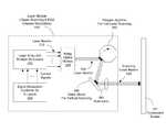
- the systemincludes a laser module 110 to produce and project at least one scanning laser beam 120 onto a screen 101 .
- the screen 101has parallel color phosphor stripes in the vertical direction where red phosphor absorbs the laser light to emit light in red, green phosphor absorbs the laser light to emit light in green and blue phosphor absorbs the laser light to emit light in blue. Adjacent three color phosphor stripes are in three different colors. One particular spatial color sequence of the stripes is shown in FIG. 1 as red, green and blue. Other color sequences may also be used.
- the laser beam 120is at the wavelength within the optical absorption bandwidth of the color phosphors and is usually at a wavelength shorter than the visible blue and the green and red colors for the color images.
- the color phosphorsmay be phosphors that absorb UV light in the spectral range from about 380 nm to about 420 nm to produce desired red, green and blue light.
- the laser module 110can include one or more lasers such as UV diode lasers to produce the beam 120 , a beam scanning mechanism to scan the beam 120 horizontally and vertically to render one image frame at a time on the screen 101 , and a signal modulation mechanism to modulate the beam 120 to carry the information for image channels for red, green and blue colors.
- Such display systemsmay be configured as rear projection systems where the viewer and the laser module 110 are on the opposite sides of the screen 101 .
- such display systemsmay be configured as front projection systems where the viewer and laser module 110 are on the same side of the screen 101 .
- FIG. 2Ashows an exemplary design of the screen 101 in FIG. 1 .
- the screen 101may include a rear substrate 201 which is transparent to the scanning laser beam 120 and faces the laser module 110 to receive the scanning laser beam 120 .
- a second front substrate 202is fixed relative to the rear substrate 201 and faces the viewer in a rear projection configuration.
- a color phosphor stripe layer 203is placed between the substrates 201 and 202 and includes phosphor stripes.
- the color phosphor stripes for emitting red, green and blue colorsare represented by “R”, “G” and “B,” respectively.
- the front substrate 202is transparent to the red, green and blue colors emitted by the phosphor stripes.
- the substrates 201 and 202may be made of various materials, including glass or plastic panels.
- Each color pixelincludes portions of three adjacent color phosphor stripes in the horizontal direction and its vertical dimension is defined by the beam spread of the laser beam 120 in the vertical direction. As such, each color pixel includes three subpixels of three different colors (e.g., the red, green and blue).
- the laser module 110scans the laser beam 120 one horizontal line at a time, e.g., from left to right and from top to bottom to fill the screen 101 .
- the laser module 110is fixed in position relative to the screen 101 so that the scanning of the beam 120 can be controlled in a predetermined manner to ensure proper alignment between the laser beam 120 and each pixel position on the screen 101 .
- the scanning laser beam 120is directed at the green phosphor stripe within a pixel to produce green light for that pixel.
- FIG. 2Bfurther shows the operation of the screen 101 in a view along the direction B-B perpendicular to the surface of the screen 101 . Since each color stripe is longitudinal in shape, the cross section of the beam 120 may be shaped to be elongated along the direction of the stripe to maximize the fill factor of the beam within each color stripe for a pixel. This may be achieved by using a beam shaping optical element in the laser module 110 .
- a laser source that is used to produce a scanning laser beam that excites a phosphor material on the screenmay be a single mode laser or a multimode laser.
- the lasermay also be a single mode along the direction perpendicular to the elongated direction phosphor stripes to have a small beam spread that is confined by the width of each phosphor stripe. Along the elongated direction of the phosphor stripes, this laser beam may have multiple modes to spread over a larger area than the beam spread in the direction across the phosphor stripe.
- This use of a laser beam with a single mode in one direction to have a small beam footprint on the screen and multiple modes in the perpendicular direction to have a larger footprint on the screenallows the beam to be shaped to fit the elongated color subpixel on the screen and to provide sufficient laser power in the beam via the multimodes to ensure sufficient brightness of the screen.
- Each of the fluorescent stripes in the fluorescent screen 101 in various examples described in this applicationis a fluorescent stripe that emits a designated color under optical excitation and can be a fluorescent stripe formed of a particular fluorescent material that emits the designed color as shown in the example in FIG. 2A .
- a fluorescent stripecan be constructed by a combination of a stripe color filter over a contiguous and uniform white fluorescent layer that is made of mixed phosphors that emit white light under optical excitation of the excitation light 120 .
- a filter layer of color filterssuch as stripes of red-transmitting, green-transmitting and blue-transmitting filters, is placed on the viewer side of the mixed phosphor layer to filter the white light and to produce colored output light.
- a fluorescent layerhas a composite structure with a filter layer and a contiguous fluorescent layer that emits white light.
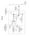
- a laser array 310 with multiple lasersis used to generate multiple laser beams 312 to simultaneously scan the screen 101 for enhanced display brightness.
- a signal modulation controller 320is provided to control and modulate the lasers in the laser array 310 so that the laser beams 312 are modulated to carry the image to be displayed on the screen 101 .
- the signal modulation controller 320can include a digital image processor that generates digital image signals for the three different color channels and laser driver circuits that produce laser control signals carrying the digital image signals.
- the laser control signalsare then applied to modulate the lasers, e.g., the currents for laser diodes, in the laser array 310 .
- the beam scanningcan be achieved by using a scanning mirror 340 such as a galvo mirror for the vertical scanning and a multi-facet polygon scanner 350 for the horizontal scanning.
- a scan lens 360can be used to project the scanning beams form the polygon scanner 350 onto the screen 101 .
- the scan lens 360is designed to image each laser in the laser array 310 onto the screen 101 .
- Each of the different reflective facets of the polygon scanner 350simultaneously scans N horizontal lines where N is the number of lasers.
- the laser beamsare first directed to the galvo mirror 340 and then from the galvo mirror 340 to the polygon scanner 350 .
- the output scanning beams 120are then projected onto the screen 101 .
- a relay optics module 330is placed in the optical path of the laser beams 312 to modify the spatial property of the laser beams 312 and to produce a closely packed bundle of beams 332 for scanning by the galvo mirror 340 and the polygon scanner 350 as the scanning beams 120 projected onto the screen 101 to excite the phosphors and to generate the images by colored light emitted by the phosphors.
- the laser beams 120are scanned spatially across the screen 101 to hit different color pixels at different times. Accordingly, each of the modulated beams 120 carries the image signals for the red, green and blue colors for each pixel at different times and for different pixels at different times. Hence, the beams 120 are coded with image information for different pixels at different times by the signal modulation controller 320 .
- the beam scanningthus maps the time-domain coded image signals in the beams 120 onto the spatial pixels on the screen 101 .
- the modulated laser beams 120can have each color pixel time equally divided into three sequential time slots for the three color subpixels for the three different color channels.
- the modulation of the beams 120may use pulse modulation techniques to produce desired grey scales in each color, a proper color combination in each pixel, and desired image brightness.
- the multiple beams 120are directed onto the screen 101 at different and adjacent vertical positions with two adjacent beams being spaced from each other on the screen 101 by one horizontal line of the screen 101 along the vertical direction.
- the beams 120may not be aligned with each other along the vertical direction on the screen 101 and may be at different positions on the screen 101 along the horizontal direction.
- the beams 120can only cover one portion of the screen 101 .
- the spinning of the polygon scanner 350causes the beams 120 from N lasers in the laser array 310 to scan one screen segment of N adjacent horizontal lines on the screen 101 .
- the galvo mirror 340is adjusted to a different fixed angular position so that the vertical positions of all N beams 120 are adjusted to scan the next adjacent screen segment of N horizontal lines. This process iterates until the entire screen 101 is scanned to produce a full screen display.
- FIG. 2Ashows one example which places the fluorescent layer 203 such as a color phosphor stripe layer between two substrates 201 and 202 .
- the screen 101couple as much light as possible in the incident scanning excitation beam 120 into the fluorescent layer with while maximizing the amount of the emitted light from the fluorescent layer that is directed towards the viewer side.
- a number of screen mechanismscan be implemented, either individually or in combination, in the screen 101 to enhance the screen performance, including efficient collection of the excitation light, maximization of fluorescent light directed towards the viewer side, enhancement of the screen contrast and reduction the screen glare.
- the structure and materials of the screen 101can be designed and selected to meet constraints on cost and other requirements for specific applications.
- the beam scanningis achieved by using the galvo mirror 340 for vertical scanning to direct an excitation beam to the polygon scanner 350 which in turn directs the excitation beam onto the screen 101 .
- the polygon scanner 350can be used to scan the excitation beam onto the galvo mirror 350 which further directs the beam to the screen 101 .
- FIGS. 4A and 4Bshow two examples of such scanning beam display systems in which the order of the polygon scanner 350 and the galvo mirror 340 is reversed from the order in FIG. 3 .
- the display in FIG. 4Buses N acousto optic modulators 410 to respectively modulate N continuous-wave (CW) excitation laser beams 312 from the laser array 310 to produce modulated laser beams 332 which carry image data.
- Other optical modulatorsmay also be used to replace the acousto optic modulators 410 .
- FIG. 5shows one example of a screen 500 that uses a contrast enhancement layer 510 on the viewer side of the fluorescent layer 520 .
- the fluorescent layer 520includes parallel phosphor stripes.
- the contrast enhancement layer 510also includes matching parallel stripes made of different materials.
- the matching stripe 511 in the contrast enhancement layer 510is made of a “red” material that transmits in a red spectral band covering the red light emitted by the red phosphor stripe 521 and absorbs or otherwise blocks other visible light including the green and blue light.
- the matching stripe in the contrast enhancement layer 510is made of a “green” material that transmits in a green spectral band covering the green light emitted by the green phosphor and absorbs or otherwise blocks other visible light including the red and blue light.
- the matching stripe in the contrast enhancement layer 510is made of a “blue” material that transmits in a blue spectral band covering the blue light emitted by the blue phosphor and absorbs or otherwise blocks other visible light including the green and red light.
- These matching parallel stripes in the contrast enhancement layer 510are labeled as “R,” “G” and “B,” respectively.
- the contrast enhancement layer 510includes different stripe filtering regions that spatially align with and match respective fluorescent regions along the direction perpendicular to the screen.
- Each filtering regiontransmits light of a color that is emitted by a corresponding matching fluorescent region and blocks light of other colors.
- Different filtering regions in the layer 510may be made of materials that absorb light of other colors different from the colors emitted by the respective matching fluorescent regions. Examples of suitable materials include dye-based colorants and pigment-based colorants.
- each filtering region in the contrast enhancement layer 510can be a multi-layer structure that effectuates a band-pass interference filter with a desired transmission band. Various designs and techniques may be used for designing and constructing such filters.
- the excitation light 120enters the fluorescent layer 520 to excite different phosphors to emit visible light of different colors.
- the emitted visible lighttransmits through the contrast enhancement layer 510 to reach the viewer.
- the ambient light 501 incident to the screen 800enters the contrast enhancement layer 510 and a portion of the incident ambient light 501 is reflected towards the viewer by passing through the contrast enhancement layer 510 for the second time. Therefore, the total optical output 502 towards the viewer includes image-carrying colored visible light emitted by the phosphor layer 520 and the reflected ambient light. This reflected ambient light does not carry image and thus tends to wash out the image produced at the phosphor layer 520 .
- the intensity of the reflected ambient lightis reduced by approximately two thirds of that of the received ambient light.
- the green and blue portions of the incident ambient light 501comprise approximately two thirds of the flux of the ambient light 501 entering a red subpixel.
- the green and blue portions of the incident ambient light 501are blocked by the contrast enhancement layer 510 .
- Only the red portion of the ambient light within the transmission band of the red filter material in the contrast enhancement layer 510transmits through the layer 510 and a part of the transmitted red ambient light is reflected back to the viewer. This part of the reflected ambient light is essentially the same color for the subpixel generated by the underlying color phosphor stripe and thus the color contrast is not adversely affected.
- each phosphor region in the fluorescent layer designcan be formed of a mixture of a fluorescent material and a color-selective absorbent material that transmits light emitted by the fluorescent material and absorbs light of other colors.
- FIG. 6Ashows another implementation that uses red, green, and blue phosphor materials with built-in contrast-enhancing capability for emitting red, green and blue light, respectively, in a common fluorescent layer 610 of parallel fluorescent stripes.
- the material for the red phosphor stripe 611is a mixture of a red phosphor capable of emitting red light and a red ink or pigment which transmits the red light and absorbs other light including the green and blue light.
- the red ink or pigmentcan have a transmission characteristic 630 as shown in FIG. 6B .
- the red ink or pigmentis mixed with the red phosphor, one of the notable characteristics is that the red ink or pigment substantially transmits ( ⁇ 100%) below the wavelength of around 420 nm in order to prevent absorbing the excitation light. Furthermore, the red ink or pigment can substantially transmit at a wavelength above around 580 nm to allow for the emitted red color from the red phosphors.
- the material for the green phosphor stripe 612is a mixture of a green phosphor emitting green light and a green ink or pigment which transmits the green light and absorbs other light including the red and blue light. Additionally, the green ink or pigment can have a transmission characteristic 640 as shown in FIG. 6C . Since the green ink or pigment is mixed with the green phosphor, one of the notable characteristics is that the green ink or pigment substantially transmits ( ⁇ 100%) below the wavelength of around 420 nm in order to prevent absorbing the excitation light. Furthermore, the green ink or pigment can substantially transmit at a wavelength window of above around 480 nm and below about 580 nm to allow for the emitted green color from the green phosphors.
- the material for the blue phosphor stripe 613is a mixture of a blue phosphor emitting blue light and a blue ink or pigment which transmits the blue light and absorbs other light including the red and green light. Additionally, the blue ink or pigment can have a transmission characteristic 650 as shown in FIG. 6D . Since the blue ink or pigment is mixed with the blue phosphor, one of the notable characteristics is that the blue ink or pigment substantially transmits ( ⁇ 100%) below the wavelength of around 480 nm in order to prevent absorbing the excitation light (below ⁇ 420 nm) and to allow for the emitted blue color from the blue phosphors.
- the contrast-enhancing fluorescent layer 610can be combined with various screen designs and configurations described in this application.
- the above described fluorescent screensuse different phosphor materials in different fluorescent stripes to produce different colors under excitation of the excitation light.
- different fluorescent stripescan be formed by the same fluorescent material that emits white light and can further include color filters to produce desired different colors from the fluorescent light.
- the contrast enhancement layer 510 in FIG. 5can be used to implement such color filters so that each color filter achieves both contrast enhancement and generation of a designated subpixel color.
- FIG. 7illustrates an example of a fluorescent screen design that has a contiguous and uniform layer 700 of mixed phosphors.
- This mixed phosphor layer 700is designed and constructed to emit white light under optical excitation of excitation light.
- the mixed phosphors in the mixed phosphor layer 700can be designed in various ways and a number of compositions for the mixed phosphors that emit white light are known and documented.
- Other non-phosphor fluorescent materials that emit white lightcan also be used for the layer 700 .
- a layer 510 of color filterssuch as stripes of red-transmitting, green-transmitting and blue-transmitting filters, is placed on the viewer side of the mixed phosphor layer 700 to filter the white light and to produce colored output towards the viewer.
- the layers 700 and 510are sandwiched between substrates 701 and 702 .
- the color filters in the layer 510may be implemented in various configurations, including in designs similar to the color filters used in color LCD panels.
- the filtertransmits the red light and absorbs light of other colors including green light and blue light.
- the screen structure in FIG. 7is simpler than other screen designs with different fluorescent stripes because the mixed phosphor layer 700 in FIG. 7 is a contiguous layer without striped spatial structures. This construction avoids alignment issues associated with aligning the filters in layer 510 with respective fluorescent stripes in the layer 520 in FIG. 5 .
- the substrate 701receives the excitation light and thus can be made of a material transparent to the excitation light, e.g., violet or UV light.
- the substrate 702faces the viewer and can be made of a material transparent to the colored light filtered by the filters in the layer 510 .
- the layer 510can be fabricated on the substrate 702 and the layer 700 can be fabricated on the substrate 701 .
- the two substrates 701 and 702can be engaged to each other to form the screen.
- an anti-reflection coating (AR)may be formed to improve the light transmission to the viewer.
- a hard protection layermay be formed over the second substrate 702 to protect the screen surface.
- UV-excitable non-phosphor organic material suitable of color or monochromatic screens described in this applicationmay be implemented with various material compositions.
- FIG. 8shows a table of representative organic materials, along with their chemical structures, colors, and fluorescent colors.
- the exemplary organic materialare Brilliantsulfoflavine FF, Basic yellow HG, Eosine, Rhodamine 6G, and Rhodamine B.
- any organic material capable of absorbing excitation lightsuch as UV light and emitting photons in the visible range at wavelengths longer than the excitation light wavelength can be used.
- UV-excitable phosphors suitable of color or monochromatic screens described in this applicationmay be implemented with various material compositions. Typically, such phosphors absorb excitation light such as UV light to emit photons in the visible range at wavelengths longer than the excitation light wavelength.
- excitation lightsuch as UV light
- red, green, and blue fluorescent materialsmay be ZnCdS:Ag, ZnS:Cu, and ZnS:Ag, respectively.
- TABLE 1lists some examples of phosphors that emit visible color light when excited by excitation light in the wavelength range from 380 nm to 415 nm described in various published patent documents. Various phosphors listed in TABLE 1 can also be excited by light from 450 nm to 470 nm. These and other phosphors can be used to implement the phosphor-based laser displays described in this application.
- phosphors described in the published PCT application No. WO 02/11173 A1are “Type I” phosphors with compositions of Eu-doped photoluminescent metal sulfides in form of MS:Eu where M is at least one of Ca, Sr, Ba, Mg and Zn, and “Type II” phosphors with compositions of metal thiometallate photoluminescent materials in form of M*N* 2 S 4 :Eu, Ce where M* is at least one of Ca, Sr, Ba, Mg and Zn, and N* is at least one of Al, Ga, In, Y, La and Gd.
- a photoluminescent metal sulfide MS(Type I phosphor) may include at least one of Ba, Mg, and Zn alone or in combination with at least one of Sr and Ca.
- a metal thiometallate photoluminescent materialmay be activated with at least one of europium (Eu) and cerium (Ce).
- Two or more of type I and type II phosphorsmay be combined, or one or more phosphors of type I and type II phosphors may be combined with other phosphors different from phosphors of type I and type II to form a phosphor blend to generate a color that may not be available from individual type I and type II phosphors.
- Such type II phosphorsemit light in the blue, green or green-yellow spectral range of the visible spectrum.
- the examples of phosphors described in U.S. Pat. No. 6,417,019include (Sr 1-u-v-x Mg u Ca v Ba x )(Ga 2-y-z AlIn z S 4 ):Eu 2+ , (Sr 1-u-v-x Mg u Ca v Ba x )(Ga.sub.2-y-z Al y In z S 4 ):Eu 2+ .
- the phosphor particlesmay be dispersed in a host material which is selected from, for example, materials including but not limited to epoxies, acrylic polymers, polycarbonates, silicone polymers, optical glasses, and chalcogenide glasses. Alternatively, such phosphors may be deposited on substrate surfaces as phosphor films.
- phosphors described in U.S. Patent Application Publication No. 2002/0185965include the phosphor powder mixed with the conventional curable silicone composition is a powder of (Y, Gd) 3 Al 5 O 12 :Ce (gadolinium and cerium doped yttrium aluminum garnet) particles available as product number QUMK58/F from Phosphor Technology Ltd., Nazeing, Essex, England.
- Particles of this phosphor materialhave a typical diameter of about 5 microns (Tm), range from 1 to 10 Tm, absorb light of wavelengths from about 430 nm to about 490 nm, and emit light in a broad band from about 510 nm to about 610 nm.
- the color of light emitted by an LED having a stenciled phosphor layeris determined, in part, by the concentration of phosphor particles in the luminescent stenciling composition.
- the phosphor particlesmay be mixed with the curable silicone polymer composition at concentrations ranging from about 20 grams of phosphor particles per 100 grams of silicone polymer composition to about 120 grams of phosphor particles per 100 grams of silicone polymer composition.
- the titanium dioxide particlesmay also be used as additives and dispersed in the silicone polymer composition at a concentration of about 1.5 grams of titanium dioxide per 100 grams of silicone polymer composition to about 5.0 grams of titanium dioxide per 100 grams of silicone polymer composition.
- the titanium dioxide particleswhich are approximately the same size as the phosphor particles, increase the scattering of excitation light and thus increase the absorption of that light by the phosphor particles.
- a thixotropic gelexhibits thixotropy, i.e., an apparent drop in viscosity when subjected to shear and a return to the original viscosity level when the shear force is removed. Consequently, a thixotropic gel behaves as a fluid when shaken, stirred, or otherwise disturbed and sets again to a gel when allowed to stand.
- the silica particlesmay be, e.g., particles of fumed silica, a colloidal form of silica made by combustion of chlorosilanes in a hydrogen-oxygen furnace. Fumed silica is chemically and physically stable at temperatures exceeding 120° C., transparent to visible light, and will impart satisfactory thixotropic properties to the luminescent stenciling composition at comparatively low concentrations. The grade of fumed silica used chosen to be compatible with non-polar materials.
- the fumed silicais M-5P grade CAB-O-SIL®. untreated amorphous fumed silica obtained from Cabot Corporation of Boston, Mass. This grade of fumed silica is hydrophobic and has an average surface area per unit mass of 200 ⁇ 15 m 2 /g.
- the M-5P grade fumed silica particlesare dispersed in the mixture of phosphor particles and silicone polymer composition with a conventional three roll mill at concentrations of about 1.5 grams of fumed silica per 100 grams of silicone polymer composition to about 4.5 grams of fumed silica per 100 grams of silicone polymer composition. As the concentration of fumed silica is increased, the stenciling composition becomes more thixotropic, i.e., more solid-like as an undisturbed gel.
- fumed silicahaving a surface area per unit mass either greater than or less than 200 ⁇ 15 m 2 /g.
- stenciling compositionsbecome more thixotropic as the surface area per unit mass of the fumed silica is increased.
- fumed silicas having lower surface area per unit massmust be used at higher concentrations.
- the required high concentrations of low surface area per unit mass fumed silicascan result in stenciling compositions having viscosities that are too high to be easily stenciled. Consequently, the fumed silica preferably has a surface area per unit mass greater than about 90 m 2 /g.
- the required concentration of fumed silicadecreases, but the fumed silica becomes more difficult to disperse in the silicone polymer composition.
- the examples of phosphors described in the PCT Patent Application Publication No. WO 01/24229include host materials and dopant ions.
- the host materialmay have an inorganic, ionic lattice structure (a “host lattice”) in which the dopant ion replaces a lattice ion.
- the dopantis capable of emitting light upon absorbing excitation radiation. Suitable dopants strongly absorb excitation radiation and efficiently convert this energy into emitted radiation.
- the dopantmay be a rare earth ion which absorbs and emits radiation via 4f-4f transitions, i.e. electronic transitions involving f-orbital energy levels.
- the first and second phosphorscomprise a host sulfide material, i.e. a lattice which includes sulfide ions.
- suitable host sulfide materialsinclude CaS, SrS and a thiogallates such as SrGa 2 S 4 .
- a phosphor mixturemay be formed by different rare earth ions that are excitable by one common blue energy source of a relatively narrow linewidth to emit light at two different energy ranges (e.g. red and green).
- the dopantis the same in the first and second phosphors with different host materials.
- the red and green emissions of the two phosphorscan be tuned by selecting an appropriate host material.
- the green phosphoris SrGa 2 S 4 :Eu.
- the red phosphoris selected from the group consisting of SrS:Eu and CaS:Eu.
- the examples of phosphors described in U.S. Patent Application Publication No. 2004/0263074include particles which are characterized as being capable of down-conversion, that is, after being stimulated (excitation) by relatively shorter wavelength light, they produce longer wavelength light (emission).
- the phosphor compositioncomprises at least one, typically at least two (or three, or four) types of phosphor particles, which each have their own emission characteristics. In an embodiment having at least two different types of phosphor particles, the first type of phosphor particle emits red light upon excitation, and the second type of phosphor particle emits green light upon excitation.
- typical phosphor particles suitable for use in the phosphor compositionmay comprise a material selected from SrS:Eu 2+ ; CaS:Eu 2+ ; CaS:Eu 2+ ,Mn 2+ ; (Zn, Cd)S:Ag + ; Mg 4 GeO 5.5 F:Mn 4+ ; Y 2 O 2 S:Eu 2+ , ZnS:Mn 2+ , and other phosphor materials having emission spectra in the red region of the visible spectrum upon excitation.
- typical phosphor particles suitable for use in the phosphor compositionmay comprise a material selected from SrGa 2 S 4 :Eu 2+ ; ZnS:Cu, Al and other phosphor materials having emission spectra in the green region of the visible spectrum upon excitation.
- blue emitting phosphor particlesmay be included in the phosphor composition in addition to the red- and green-emitting phosphors; suitable blue emitting phosphor particles may comprise, e.g. BaMg 2 Al 16 O 27 :Eu 2+ ,Mg or other phosphor materials having emission spectra in the blue region of the visible spectrum upon excitation.
- the phosphor compositionmay comprise a type of phosphor particles that is selected to produce yellow light upon excitation.
- phosphor particles suitable for use in the phosphor compositionmay include a material selected from (Y, Gd) 3 Al 5 O 12 :Ce, Pr and other phosphor materials having emission spectra in the yellow region of the visible spectrum upon excitation.
- Some suitable red-emitting phosphor particlesmay have a peak emission wavelength in the range of about 590 nm to about 650 nm.
- the phosphor particleshave a peak emission wavelength in the range of about 620 nm to about 650 nm, typically in the range of about 625 nm to about 645 nm, more typically in the range of about 630 nm to about 640 nm.
- the phosphor particleshave a peak emission wavelength in the range of about 590 nm to about 625 nm, typically in the range of about 600 nm to about 620 nm.
- the phosphor particlesmay emit light having a wavelength in the range of about 600 nm to about 650 nm, typically in the range of about 610 nm to about 640 nm, more typically in the range of about 610 nm to about 630 nm.
- Some suitable green-emitting phosphor particlesmay have a peak emission wavelength in the range of about 520 nm to about 550 nm.
- the phosphor particleshave a peak emission wavelength in the range of about 530 nm to about 550 nm, typically in the range of about 535 nm to about 545 nm.
- the phosphor particleshave a peak emission wavelength in the range of about 520 nm to about 535 nm.
- the phosphor particlesemit light having a wavelength in the range of about 520 nm to about 550 nm, typically in the range of about 535 nm to about 550 nm, or in the range of about 520 nm to about 535 nm.
- Some suitable blue-emitting phosphor particlestypically have a peak emission wavelength in the range of about 440 nm to about 490 nm.
- the phosphor particleshave a peak emission wavelength in the range of about 450 nm to about 470 nm, typically in the range of about 455 nm to about 465 nm.
- the phosphor particleshave a peak emission wavelength in the range of about 440 nm to about 450 nm, typically in the range of about 435 nm to about 445 nm.
- the phosphor particlesemit light having a wavelength in the range of about 440 nm to about 480 nm, typically in the range of about 450 nm to about 470 nm.
- Some suitable yellow-emitting phosphor particlestypically have a peak emission wavelength in the range of about 560 nm to about 580 nm.
- the phosphor particleshave a peak emission wavelength in the range of about 565 nm to about 575 nm.
- the phosphor particleshave a peak emission wavelength in the range of about 575 nm to about 585 nm.
- the phosphor particlesemit light having a wavelength in the range of about 560 nm to about 580 nm, typically in the range of about 565 nm to about 575 nm.
- the exact wavelength range for each of the above described type of phosphor particlesmay be determined by selection from available sources of phosphors, desired color attributes of the light emitting device (e.g. the ‘correlated color temperature’ of the emitted white light), choice of the excitation light such as the excitation wavelength, and the like.
- Useful phosphor materials and other informationmay be found in Mueller-Mach et al., “High Power Phosphor-Converted Light Emitting Diodes Based on III-Nitrides”, IEEE J. Sel. Top. Quant. Elec. 8(2):339 (2002).
- the examples of phosphors described in the published PCT Application No. PCT/US99/28279include Ba 2 MgSi 2 O 7 :Eu 2+ ; Ba 2 SiO 4 : Eu 2+ ; and (Sr, Ca, Ba)(Al, Ga) 2 S 4 : Eu 2+ , where the element following the colon represents an activator.
- x, y, and zare all nonzero.
- x and yare both nonzero.
- Examples of green emitting phosphorsmay have peak emissions between about 500 nm and about 555 nm.
- Ba 2 MgSi 2 O 7 :Eu 2+has a peak emission at about 495-505 nm, typically about 500 nm
- Ba 2 SiO 4 : Eu2+has a peak emission at about 500-510 nm, typically about 505 nm
- (Sr, Ca, Ba)(Al, Ga) 2 S 4 :Eu 2+has a peak emission at about 535-545 nm, typically about 540 nm.
- phosphors described in U.S. Patent Application Publication No. 2001/0050371include fluorescent materials that include a CaS phosphor activated by Eu, phosphors represented by AEu (1-x) Ln x B 2 O 8 where A is an element selected from the group consisting of Li, K, Na and Ag; Ln is an element selected from the group consisting of Y, La and Gd; and B is W or Mo; and x is number equal to or larger than 0, but smaller than 1.
- a CaS phosphor activated by Eu or a phorsphor of AEu (1-x) Ln x B 2 O 8may be mixed with a base polymer to form a transparent resin.
- a red phosphor that emits red lightmay be CaS activated by Eu or a compound expressed by a general formula AEu (1-x) Ln x B 2 O 8 .
- CaS activated by Euis excited by light of 420 to 600 nm and emits light of 570 to 690 nm which peaks at 630 nm.
- AEu (1-x) Ln x B 2 O 8is a phosphor which emits light near 614 nm by transition of Eu 3+ ions.
- the red phosphorscan be excited by light near 470 nm (blue) and or 540 nm (green) and can emit light near 620 nm (red).
- xis zero, the phosphor AEuB 2 O 8 is formed and exhibits the highest emission intensity near 615 nm (red).
- a yttrium aluminate phosphorcan be a stable oxide having a garnet structure in which Y-atoms of Y 3 Al 5 O 12 are substituted by Gd at part of their positions, particularly a phosphor which is excited by blue light (400 to 530 nm) to emit light of yellow to green region centering 550 nm.
- Activating elements to be added to the yttrium aluminate phosphorinclude, for example, cerium, europium, manganese, samarium, terbium, tin, chromium, etc.
- CeY x Gd 3-x Al 5 O 12 activated by Ce may be used.
- one, two or more kinds of such YAG phosphorsmay be mixed together to form a desired phosphor material.
- the examples of phosphors described in U.S. Pat. No. 6,252,254include YBO 3 :Ce 3+ ,Tb 3+ ; BaMgAl 10 O 17 :Eu 2+ ,Mn 2+ ; (Sr, Ca, Ba)(Al, Ga) 2 S 4 :Eu 2+ ; and Y 3 Al 5 O 12 :Ce 3+ ; and at least one of: Y 2 O 2 S:Eu 3+ ,Bi 3+ ; YVO 4 :Eu 3+ ,Bi 3+ ; SrS:Eu 2+ ; SrY 2 S 4 :Eu 2+ ; SrS:Eu 2+ ,Ce 3+ ,K + ; (Ca, Sr)S:Eu 2+ ; and CaLa 2 S 4 :Ce 3+ , where the element following the colon represents an activator.
- the SrS:Eu 2+ ,Ce 3+ ,K + phosphorwhen excited by blue light, emits a broadband spectrum including red light and green light.
- These phosphor compositionscan be used to produce white light with pleasing characteristics, such as a color temperature of 3000-4100° K, a color rendering index of greater than 70, typically greater than 80, for example about 83-87, and a device luminous efficacy of about 10-20 lumens per watt of input electric power when blue LED is used as the excitation source.
- phosphors described in U.S. Patent Application Publication No. 2002/0003233include a single crystal Cerium-doped Yttrium-Aluminum-Garnet (Y 3 Al 5 O 12 :Ce 3+ ) compound as a yellowish-light-emitting phosphor.
- Yttrium-Aluminum-Oxideswhich do not have garnet structures, such as monoklinic YalO and YalO-perovskite, may also be used as the host materials for the phosphors.
- Several lanthanides (Ln)may partly replace the Yttrium, such as in (Y, Ln)AlO, (Y, Ln)(Al, Ga)O.
- the lanthanidemay be, for example Lutethium (Lu).
- These host materialsmay be doped with single dopants such as Cerium (Ce), Praseodymium (Pr), Holmium (Ho), Ytterbium (Yb), and Europium (Eu), or with double dopants such as (Ce, Pr), (Ce, Ho), and (Eu, Pr) to form various phosphors.
- Y 3 Al 5 O 12 :Pr 3+are examples of single crystal phosphor materials.
- a phosphor listed aboveemits yellowish light by absorbing either bluish light or ultraviolet light having a wavelength that is shorter than or equal to about 460 nm.
- a YAG substrate doped with 4 mol % Cerium (Ce 3+ )can absorb light having a wavelength of about 410-460 nm and emit yellowish light having a peak wavelength of about 550-570 Tm. any.
- Part of the Yttrium in YAGmay be substituted by a lanthanide element such as Gadolinium (Gd).
- a phosphormay be (Y 0.75 Gd 0.25 ) AG:Ce.
- phosphors described in European Patent Application No. 1,150,361include a resin comprising a phosphor selected from the phosphor family chemically identified as (Sr, Ca, Ba)S:Eu 2+ .
- One phosphor selected from this familyis strontium sulfide doped with europium, which is chemically defined as SrS:Eu 2+ and has a peak emission at 610 nm.
- other types of phosphor converting elementsmay also be used, including phosphor-converting thin films, phosphor-converting substrates, or various combinations of these elements.
- phosphors described in U.S. Patent Application Publication No. 2002/0145685include a red phosphor SrS:Eu 2+ and a green phosphor SrGa 2 S 4 :Eu 2+ . These phosphors are excitable by the 460 nm blue light.
- the examples of phosphors described in U.S. Patent Application Publication No. 2005/0001225include rare-earth element doped oxide nitride phosphor or cerium ion doped lanthanum silicon nitride phosphor.
- a rare-earth element doped oxide nitride in the following examplesis a crystalline material, not including a glass material such as oxynitride glass. However, it may include a small amount of glass phase (e.g., less than 5%).
- a cerium ion doped lanthanum silicon nitride in the following examplesis a crystalline material, not including a glass material.
- One example of a first phosphoris single-phase 1-sialon phosphor that is represented by: Me X Si 12-(m+n) Al (m+n) OnN 16-n :Re1 y Re2 z .
- metal (Me)Me is one or more of Li, Ca, Mg, Y and lanthanide metals except for La and Ce
- lanthanide metal (Re1)Re1 is one or more of Ce, Pr, Eu, Tb, Yb and Er
- Re1is one or more of Ce, Pr, Eu, Tb, Yb and Er
- Re1lanthanide metal
- Re2lanthanide metal
- Memay be one or more of Ca, Y and lanthanide metals except for La and Ce.
- Memay be Ca or Nd.
- the lanthanide metal (Re1) used for replacingmay be Ce, Eu or Yb.
- two kinds of metals for replacingfor example, a combination of Eu and Er may be used.
- three kinds of metals for replacingfor example, a combination of Eu, Er and Yb may be used.
- the metal (Me)may be replaced by lanthanide metal Re1 and lanthanide metal Re2 as co-activator.
- the lanthanide metal Re2is dysprosium (Dy).
- the lanthanide metal Re1may be Eu.
- the metal (Me)replaced by one or more of Ce, Pr, Eu, Tb. Yb and Er (lanthanide metal (Re1)), or one or more of Ce, Pr, Eu, Tb, Yb and Er (lanthanide metal (Me) (Re1)) and Dy (lanthanide metal (Re2)
- the metalis not necessarily added and may be replaced by another metal.
- A-sialon (I-sialon)has a higher nitrogen content than oxynitride glass and is represented by: N x Si 12-(m ⁇ n) Al (m+n ⁇ ) O n N 16-n where x is a value obtained dividing (m) by a valence of metal (M).
- oxynitride glassis as described in prior art 3, such a phosphor that serves to shift the position of excitation/emission peak of conventional oxide system phosphors to the longer wavelength side by replacing oxygen atom surrounding the rare-metal element as luminescence center by nitrogen atom to relax the influence of surrounding atoms to electron of rare-metal element, and that has an excitation spectrum extending until visible region ( ⁇ 500 Tm).
- the metal (Me)is dissolved in the range of, at the minimum, one per three unit cells of I-sialon including four mass weights of (Si, Al) 3 (N, O) 4 to, at the maximum, one per one unit cell thereof.
- the solid solubility limitis generally, in case of bivalent metal (Me), 0.6 ⁇ m ⁇ 3.0 and O ⁇ n ⁇ 1.5 in the above formula and, in case of trivalent metal (Me), 0.9 ⁇ m ⁇ 4.5 and O ⁇ n ⁇ 1.5. It is estimated that, in a region except for those regions, single-phase I-sialon phosphor is not obtained.
- the interionic distance of lanthanide metal Re1 as luminescence center to replace part or all of metal (Me) and to serve as activatoris about 5 angstroms at the minimum. It is significantly greater than 3 to 4 angstroms in phosphor known thus far. Therefore, it can prevent a significant reduction in emission intensity due to concentration quenching generated when a high concentration of lanthanide metal as luminescence center is included in matrix material.
- the metal (Me)is replaced by lanthanide metal (Re2) as I-activator as well as lanthanide metal (Re1) as luminescence center. It is assumed that lanthanide metal (Re2) has two co-activation effects. One is sensitizer function and the other is to newly generate a carrier trap level to develop or improve the long persistence or to improve the thermal luminescence. Since the lanthanide metal Re2 is co-activator, it is suitable that the replacement amount thereof is generally 0.0 ⁇ z ⁇ 0.1 in the earlier formula.
- the single-phase I-sialon phosphorhas I-sialon as a matrix material, and is essentially different in composition and crystal structure from a phosphor having ⁇ -sialon as matrix material.
- ⁇ -sialonis represented by: Si 6-z Al z O z N 8-z (0 ⁇ z ⁇ 0.2), and it is solid solution of ⁇ -type silicon nitride where part of Si sites is replaced by Al and part of N sites is replaced by O.
- I-sialonis represented by: Me X Si 12-(m+n) Al (m+n) O n N 16-n , and it is a solid solution of I-type silicon nitride, where part of Si—N bonds is replaced by Al—N bond and a specific metal (Me) (Me is one or more of Li, Ca, Mg, Y and lanthanide metals except for La and Ce) invades between lattices and is dissolved therein.
- Mespecific metal
- the ⁇ -sialonhas a high oxygen content and the I-sialon has a high nitrogen content.
- a phosphoris synthesized using ⁇ -sialon as matrix material and adding one or more of rare-earth oxides of Ce, Pr, Eu, Tb, Yb and Er as luminescence center, it becomes a mixed material that has a compound including a rare-earth metal between ⁇ -sialon particles since the ⁇ -sialon does not dissolve metal.
- the metal (Me)(Me is one or more of Li, Ca, Mg, Y and lanthanide metals except for La and Ce) is taken and dissolved in the crystal structure and the metal (Me) is replaced by rare-earth metal, Ce, Pr, Eu, Tb, Yb and Er as luminescence center. Therefore, the oxide nitride phosphor composed of single-phase I-sialon structure can be obtained.
- composition and crystal structure of phosphordrastically changes by whether to use ⁇ -sialon or I-sialon as matrix material. This is reflected in emission characteristics of phosphor.
- a phosphor that is synthesized adding Er oxide to ⁇ -sialonradiates a blue luminescent light (410-440 nm).
- I-sialonas described later, rare-earth element doped oxide nitride phosphor radiates orange to red light (570-590 nm) due to the activation of Er.
- Eris taken in the crystal structure of I-sialon and, thereby, Er is influenced by nitrogen atom composing the crystal and, therefore, the elongation of light source wavelength, which is very difficult to realize in phosphor with oxide as matrix material, can be easily generated.
- the rare-earth element doped oxide nitride phosphoralso has the advantages of matrix material, I-sialon. Namely, I-sialon has excellent thermal and mechanical properties and can prevent the thermal relaxation phenomenon that causes a loss in excitation energy. Therefore, in the rare-earth element doped oxide nitride phosphor, a ratio of reduction in emission intensity according to rise of temperature becomes small. Thus, the temperature range available can be broadened as compared to the conventional phosphor.
- the rare-earth element doped oxide nitride phosphorcan be excited by ultraviolet rays to X-rays further electron beam, according to O/N ratio in its composition, selection of lanthanide metal Re1 to replace metal (Me), and existence of lanthanide metal Re2 as I-activator.
- an example of a second phosphoris a rare-earth element doped oxide nitride phosphor that contains I-sialon as main component (hereinafter referred to as mixture I-sialon phosphor).
- This second phosphorincludes I-sialon, which dissolves a rare-earth element allowing an increase in brightness of a white LED using blue LED chip as light source, ⁇ -sialon, and unreacted silicon nitride.
- a mixture material with a property equal to single-phase I-sialon phosphoris found that is composed of I-sialon that part of Ca site in I-sialon stabilized by Ca is replaced by one or more of rare-earth metal (M) (where M is Ce, Pr, Eu, Tb, Yb or Er), ⁇ -sialon and unreacted silicon nitride.
- Mis preferably Ce, Eu or Yb and further preferably Ce or Eu.
- the mixture I-sialon phosphorcan be produced adding less rare-earth element than the single-phase I-sialon phosphor. Thus, the material cost can be reduced. Further, since the mixture I-sialon phosphor also has I-sialon as matrix material like the single-phase I-sialon phosphor, it can have the advantages of matrix material I-sialon, i.e. good chemical, mechanical and thermal properties. Thus, it offers a stable and long-lifetime phosphor material. Due to these properties, it can suppress thermal relaxation phenomenon causing a loss in excitation energy. Therefore, in I-sialon with dissolved rare-earth element as well as Ca in this embodiment, a ratio of reduction in emission intensity according to rise of temperature becomes small. Thus, the temperature range available can be broadened as compared to the conventional phosphor.
- the mixture I-sialon phosphorcan be excited by ultraviolet rays to X-rays further electron beam, according to O/N ratio in its composition and selection of metal (M).
- the mixture I-sialon phosphoroffers a material that has an emission property equal to the single-phase I-sialon phosphor even when reducing the amount of rare-earth metal added.
- itis necessary to dissolve more than a certain amount of element.
- amounts of Ca and trivalent metal dissolvedare given x and y, respectively, a value of (x+y) is needed to be greater than 0.3 in thermodynamic equilibrium.
- the mixture I-sialon phosphorincludes an organ with ⁇ -sialon and unreacted silicon nitride remained other than single-phase I-sialon phosphor because of less addition amount and not reaching the thermodynamic equilibrium.
- the amount of added metal in the mixture I-sialon phosphoris in the range of 0.05 ⁇ (x+y) ⁇ 0.3, 0.02 ⁇ x ⁇ 0.27 and 0.03 ⁇ y ⁇ 0.3 in chemical composition of powder. If the amount of added metal is less than the lower limit, the amount of I-sialon lowers and the emission intensity lowers. If the amount of added metal is greater than the upper limit, only I-sialon remains. Therefore, the object of high brightness can be completed.
- the mixture I-sialon phosphorcan be obtained that is composed of: I-sialon of 40 weight % or more and 90 weight % or less; ⁇ -sialon of 5 weight % or more and 40 weight % or less; and unreacted silicon nitride of 5 weight % or more and 30 weight % or less.
- the reason why the emission intensity is high even with the unreacted silicon nitride includedis that I-sialon epitaxially grows on unreacted silicon nitride and its surface portion mainly responds to excitation light to offer an emission property substantially equal to only I-sialon.
- the rangemay be 0.15 ⁇ (x+y) ⁇ 0.3, 0.10 ⁇ x ⁇ 0.25 and 0.05 ⁇ y ⁇ 0.15.
- the mixture I-sialon phosphorcan be obtained that is composed of: I-sialon of 50 weight % or more and 90 weight % or less; ⁇ -sialon of 5 weight % or more and 30 weight % or less; and unreacted silicon nitride of 5 weight % or more and 20 weight % or less.
- the mixture I-sialon phosphorcan be obtained by, e.g., heating Si 3 N 4 -M 2 O 3 —CaO—AlN—Al 2 O 3 system mixed powder at 1650 to 1900° C. in inert gas atmosphere to get a sintered body, then powdering it. Since CaO is so instable that it easily reacts with moisture vapor in the air, it is generally obtained by adding in the form of calcium carbonate or calcium hydroxide, then making it CaO in the process of heating at high temperature.
- the chemical composition of mixture I-sialon phosphorcan be defined using the composition range of M-I-sialon, Ca—I-sialon and ⁇ -sialon. Namely, in the range of three composition lines of Si 3 N 4 -a(M 2 O 3 .9AlN), Si 3 N 4 -b(CaO.3AlN) and Si 3 N 4 -c(AlN.Al 2 O 3 ), it is defined 4 ⁇ 10 ⁇ 3 ⁇ a ⁇ 4 ⁇ 10 ⁇ 2 , 8 ⁇ 10 ⁇ 3 ⁇ b ⁇ 8 ⁇ 10 ⁇ 1 and 10 ⁇ 2 ⁇ c ⁇ 8 ⁇ 10 ⁇ 1 .
- a third phosphoris a cerium ion doped lanthanum silicon nitride phosphor: La 1-X Si 3 N 5 :xCe (doping amount x is 0 ⁇ x ⁇ 1), where lanthanum site is replaced in solid dissolution by cerium ion activator. If the doping amount is 0.1 ⁇ x ⁇ 0.5, it is ultraviolet light excitation phosphor and, if the doping amount is 0.0 ⁇ x ⁇ 0.2, it is electron beam excitation phosphor.
- Lanthanum silicon nitride (LaSi 3 N 5 )has an excellent thermal stability and serves to suppress the thermal relaxation phenomenon in the process of phosphor emission. Therefore, a loss in excitation energy can be reduced and a ratio of reduction in emission intensity according to rise of temperature becomes small. Thus, in the cerium ion doped lanthanum silicon nitride phosphor, the temperature range available can be broadened as compared to the conventional phosphor. Also, the lanthanum silicon nitride (Lasi 3 N 5 ) has excellent chemical stability and is light resistance.
- the cerium ion doped lanthanum silicon nitride phosphorsatisfies a blue chromaticity value and has excellent thermal stability, mechanical property and chemical stability. Therefore, it can have great potential in applications for fluorescent character display tube (VFD), field emission display (FED) etc. that may be used in severe environment.
- VFDfluorescent character display tube
- FEDfield emission display
- the examples of phosphors described in U.S. Pat. No. 5,998,925include a garnet fluorescent material comprising 1) at least one element selected from the group consisting of Y, Lu, Sc, La, Gd and Sm, and 2) at least one element selected from the group consisting of Al, Ga and In, and being activated with cerium.
- Y 3 Al 5 O 12 :Ce and Gd 3 In 5 O 12 :Ceare two examples. The presence of Y and Al enables a phosphoer to increase the luminance.
- part of Almay be substituted by Ga so that the proportion of Ga:Al is within the range from 1:1 to 4:6 and part of Y is substituted by Gd so that the proportion of Y:Gd is within the range from 4:1 to 2:3.
- phosphorexamples include (Re 1-r Sm r ) 3 (Al 1-s Ga s ) 5 O 12 :Ce, where 0 ⁇ r ⁇ 1 and 0 ⁇ s ⁇ 1 and Re is at least one selected from Y and Gd, (Y 1-p-q-r Gd p Ce q Sm r ) 3 (Al 1-s Ga s ) t O 12 as the phosphor, where 0 ⁇ p ⁇ 0.8, 0.003 ⁇ q ⁇ 0.2, 0.0003 ⁇ r ⁇ 0.08 and 0 ⁇ s ⁇ 1.
- a phosphormay include two or more yttrium-aluminum-garnet fluorescent materials, activated with cerium, of different compositions including Y and Al to control the emission spectrum of the phosphor.
- a phosphormay include a first fluorescent material represented by general formula Y 3 (Al 1-s Ga s ) 5 O 12 :Ce and a second fluorescent material represented by the formula Re 3 Al 5 O 12 :Ce, where 0 ⁇ s ⁇ 1 and Re is at least one selected from Y, Ga and La.
- two or more fluorescent materials of different compositionsrepresented by a general formula (Re 1-r Sm r ) 3 (Al 1-s Ga s ) 5 O 12 :Ce, where 0 ⁇ r ⁇ 1 and 0 ⁇ s ⁇ 1 and Re is at least one selected from Y and Gd may be used as the phosphor in order to control the emitted light to a desired wavelength.
- phosphors described in U.S. Pat. No. 6,765,237include phosphors that absorb UV light from about 380 to about 420 nm and emit visible light of different colors.
- a phosphor blendmay include a first phosphor comprising BaMg 2 Al 16 O 27 :Eu 2+ (BAM) and a second phosphor comprising (Tb.
- Ais a member selected from the group consisting of Y, La, Gd, and Sm
- REis a member selected from the group consisting of Ce, Pr, Nd, Sm, Eu, Gd, Dy, Ho, Er, Tm, Yb, and Lu
- Dis a member selected from the group consisting of Al, Ga, and In
- xis in the range from 0 to about 0.5
- yis in the range from about 0 to about 0.2
- zis in the range from about 4 to about 5.
- a phosphor blendmay include a first phosphor comprising Tb 3 Al 4.9 O 12 :Ce and a second phosphor selected from the group consisting of BaMg 2 Al 16 O 27 :Eu 2+ (BAM) and (Sr, Ba, Ca, mg) 5 (PO 4 ) 3 Cl: Eu 2+
- a rare earth element activated complex halide phosphorrepresented by the formula: BaF 2 .a BaX 2 .bMgF 2 .cBeF 2 .dMe II F 2 :eLn, where X is at least one halogen selected from the group consisting of chlorine, bromine and iodine; Me II is at least one divalent metal selected from the group consisting of: calcium and strontium; Ln is at least one rare earth element selected from the group consisting of: divalent europium (Eu 2+ ), cerium (Ce 3+ ) and terbium (Tb 3+ ), and a is in the range between 0.90 and 1.05, b is in the range of 0 to 1.2; c is in the range of between 0 and 1.2, and d is defined by the sum of c+d being in the range of between 0 and 1.2, and BeF 2 is present in an amount sufficient to effect a phosphor exhibiting a higher luminance than said phosphor absent BeF 2
- a cerium activated rare earth halophosphate phosphorhaving the formula: LnPO 4 .aLnX 3 :xCe 3+ in which Ln is at least one rare earth element selected from the group consisting of Y, La, Gd and Lu; X is at least one halogen selected from the group consisting of F, Cl, Br and I; and a and x are numbers satisfying the conditions of 0.1 ⁇ a ⁇ 10.0 and 0 ⁇ x ⁇ 0.2, respectively and exhibiting a higher stimulated emission upon excitation with a He—Ne laser of a wavelength 632.8 nm after exposure to X-rays at 80 KVp, than the phosphor wherein a is less than 0.1. See U.S. Pat. No. 4,661,419 for additional details.
- a mixed single-phase strontium and lanthanide oxide with a magnetolead type crystalline structurehaving the formula (I): Sr x Ln1 y1 Ln2 y2 Ln3 y3 M z A a B b O 19-k(I) in which Ln1 represents at least one trivalent element selected from lanthanum, gadolinium and yttrium; Ln2 represents at least one trivalent element selected from neodymium, praseodymium, erbium, holmium and thulium; Ln3 represents an element selected from bivalent europium or trivalent cerium with retention of electric neutrality by virtue of oxygen holes; M represents at least one bivalent metal selected from magnesium, manganese, and zinc; A represents at least one trivalent metal selected from aluminum and gallium; B represents at least one trivalent transition metal selected from chromium and titanium; x, y1, y2, y3, z, a, b and k represent numbers so that 0 ⁇
- a divalent europium activated alkaline earth metal halide phosphorhaving the formula: M II X 2 .aM II X′ 2 .bSiO:xEu 2+ in which M II is at least one alkaline earth metal selected from the group consisting of Ba, Sr and Ca; each of X and X′ is at least one halogen selected from the group consisting of Cl, Br and I, and X is not the same as X′; a and x are numbers satisfying the conditions of 0.1 ⁇ a ⁇ 10.0 and 0 ⁇ x ⁇ 0.2, respectively; and b is a number satisfying the condition of 0 ⁇ b ⁇ 3 ⁇ 10 ⁇ 2 . See U.S. Pat. No. 5,198,679 for additional details.
- a bright, short wavelength blue-violet phosphor for electro luminescent displayscomprising an alkaline-based halide as a host material and a rare earth as a dopant. See U.S. Pat. No. 5,602,445.
- the host alkaline chloridecan be chosen from the group II alkaline elements, particularly SrCl 2 or CaCl 2 , which, with a europium or cerium rare earth dopant, electroluminesces at a peak wavelength of 404 and 367 nanometers respectively.
- the resulting emissionshave CIE chromaticity coordinates which lie at the boundary of the visible range for the human eye thereby allowing a greater range of colors for full color flat panel electroluminescent displays.
- An inorganic thin film electroluminescent devicecomprising an inorganic light emission layer, a pair of electrodes and a pair of insulating layers, at least one of the electrodes being optically transparent, the light emission layer being positioned between the pair of insulating layers, each insulating layer being formed on an opposite side of the light emission layer, the pair of insulating layers being positioned between a light emission layer and the pair of electrodes, the light emission layer consisting essentially of inorganic material comprising a matrix of lanthanum fluoride doped with at least one member selected from the group consisting of: rare earth element metals and compounds thereof. See U.S. Pat. No. 5,648,181 for additional details.
- a radiographic phosphor screencomprising a support and, coated on the support, at least one layer forming a luminescent portion and an overcoat layer, the luminescent portion and overcoat layer including a binder that is transparent to X-radiation and emitted light and said luminescent portion including phosphor particles in a weight ratio of phosphor particles to binder of 7:1 to 25:1.
- the phosphorcomprises oxygen and a combination of species characterized by the relationship: (Ba 1-q M q )(Hf 1-z-e Zr z Mg e ): yT wherein M is selected from the group consisting of Ca and Sr and combinations thereof; T is Cu; q is from 0 to 0.15; z is from 0 to 1; e is from 0 to 0.10; z+e is from 0 to 1; an y is from 1 ⁇ 10 ⁇ 6 to 0.02. See U.S. Pat. No. 5,698,857 for additional details.
- a garnet fluorescent materialcomprising: 1) at least one element selected from the group consisting of Y, Lu, Se, La, Gd and Sm; and 2) at least one element selected from the group consisting of Al, Ga and In, and being activated with cerium.
- a wavelength-converting casting compositionfor converting a wavelength of ultraviolet, blue or green light emitted by an electroluminescent component, comprising: a) a transparent epoxy casting resin; b) an inorganic luminous substance pigment powder dispersed in the transparent epoxy resin, the pigment powder comprising luminous substance pigments from a phosphorus group having the general formula: A 3 B 5 X 12 :M, where A is an element selected from the group consisting of Y, Ca, Sr; B is an element selected from the group consisting of Al, Ga, Si; X is an element selected from the group consisting of O and S; and M is an element selected from the group consisting of Ce and Tb.
- the luminous substance pigmentshave grain sizes ⁇ 20 Tm and a mean grain diameter d 50 ⁇ 5 Tm. See U.S. Pat. No. 6,066,861 for additional details.
- UV-excitable phosphors for emitting green, red, and blue colorsare Ca 8 Mg(SiO 4 ) 4 Cl 2 :Eu 2+ , Mn 2+ ; Y 2 O 3 :Eu 3+ , Bi 3+ ; and Ba 2 (Sr, Ba, Ca) 5 (PO 4 ) 3 Cl:Eu 2+ (or BaMg 2 Al 16 O 27 : Eu 2+ ); respectively. See U.S. Pat. No. 6,255,670 for additional details.
- the U.S. Patent Application Publication No. 2004/0227465also discloses phosphors represented by Sr x Ba y Ca z SiO 4 :Eu 2+ in which x, y, and z are each independently any value between 0 and 2, including 0 and 2.
- divalent Euwhich serves as an activator, is present in any amount between 0.0001% and about 5% in mole percent based on the total molar weight of said composition.
- the activator, Eumay be present in any amount between 0.0001% and 5.00% in mole percent based on the total molar weight of the composition, including every thousandth percentage therebetween.
- the parameters x, y and zare 0.5 ⁇ x ⁇ 1.5; 0 ⁇ y ⁇ 0.5; and 0.5 ⁇ z ⁇ 1.5 in the above formula. In yet other implementations, the parameters x, y and z are 1.5 ⁇ x ⁇ 2.5; 0 ⁇ y ⁇ 0.5; and 0 ⁇ z ⁇ 0.5 in the above formula.
- the parameters x, y and zmay also be 1.0 ⁇ x ⁇ 2.0; 0 ⁇ y ⁇ 1.0; and 0 ⁇ z ⁇ 0.5 in the above formula.
- the above phosphor Sr x Ba y Ca z SiO 4 :Eu 2+may further include at least one additional element selected from the group consisting of: Ce, Mn, Ti, Pb, and Sn.
- such an additional elementis present in the phosphor in any amount between 0.0001% and 5.00% in mole percent based upon the total molar weight of the phosphor.
- the examples of phosphors described in U.S. Patent Application Publication No. 2005/0023962include ZnS x Se y :Cu, A in which x and y are each independently any value between 0 and 1 and A is at least one of Ag, Al, Ce, Tb, Cl, I, Mg, Mn.
- the monovalent Cu, which serves as the main activatormay be present in any amount between 0.0001% and about 5% in mole percent based on the total molar weight of said composition.
- the activator, Cumay be present in any amount between 0.0001% and 5.00% in mole percent based on the total molar weight of the composition, including every thousandth percentage therebetween.
- the parameters x, y and zare 0.5 ⁇ x ⁇ 1 and 0 ⁇ y ⁇ 0.5 in the above formula. In other implementations, the parameters x, y and z are 0 ⁇ x ⁇ 0.5 and 0 ⁇ y ⁇ 0.5 in the above formula. The parameters x, y and z may also be 0 ⁇ x ⁇ 0.5 and 0.5 ⁇ y ⁇ 1.0 in the above formula.
- phosphors described in U.S. Patent Application Publication No. 2005/023963include thioselenide and/or selenide-based fluorescent materials which are capable of absorbing with high efficiency blue, violet, or ultraviolet (UV) light and emitting light of a wavelength longer than that absorbed from the light source.
- phosphor materialsmay be manufactured to emit broad color spectra that can be tuned from blue to green to yellow and red emissions. Two or more phosphors may be mixed in order to achieve a specific, desired white color performance.
- the divalent Euwhich can serve as the main activator, may be present in any amount between 0.0001% and about 10% in mole percent based on the total molar weight of said composition.
- the activator, Eumay be present in any amount between 0.0001% and 10.00% in mole percent based on the total molar weight of the composition, including every thousandth percentage therebetween.
- the parameters x, y, and zare 0.5 ⁇ x ⁇ 1 and 0 ⁇ y ⁇ 0.5 in the above formula.
- the parameter x, y and zare 0 ⁇ x ⁇ 5 and 0.5 ⁇ y ⁇ 1.0 in the above formula.
- xis about 0 and y is about 1 in the above formula, or x is about 1 and y is about 0 in the above formula.
- the divalent Euwhich can serve as the main activator, may be present in any amount between 0.0001% and about 10% in mole percent based on the total molar weight of said composition.
- the activator, Eumay be present in any amount between 0.0001% and 10.00% in mole percent based on the total molar weight of the composition, including every thousandth percentage there between.
- M1comprises an element selected from the group consisting of: Be, Mg, Ca, Sr, Ba, Zn
- M2comprises an element selected from the group consisting of: Be, Mg, Ca, Sr, Ba, Zn
- Acomprises one or more elements selected from the group consisting of: Al, Ga, In, Y, La, and Gd
- Bcomprises one or more elements selected from the group consisting of: Eu, Ce, Cu, Ag, Al, Tb, Cl, Br, F, I, Mg, Pr, K, Na, and Mn.
- Bmay be present in any amount between 0.0001% and about 10% in mole percent based on the total molar weight of said composition, and wherein x and y are each independently any value between 0 and 1, subject to the provisos that the sum of x and y is equal to any number in the range of between about 0.75 and about 1.25, the sum of m and n is about 1, and M1 is different than M2.
- the parameters x and yare 0.5 ⁇ x ⁇ 1 and 0 ⁇ y ⁇ 0.5 in the above formula.
- the parameters x and yare 0 ⁇ x ⁇ 0.5 and 0 ⁇ y ⁇ 0.5, or 0 ⁇ x ⁇ 0.5 and 0.5 ⁇ y ⁇ 1.0, or x is about 0.75 and y is about 0.25, or x is about 0 and y is about 1, or x is about 1 and y is about 0 in the above formula.
- M1comprises an element selected from the group consisting of: Be, Mg, Ca, Sr, Ba, Zn
- M2comprises an element selected from the group consisting of: Be, Mg, Ca, Sr, Ba, Zn
- Acomprises one or more elements selected from the group consisting of: Al, Ga, In, Y, La, and Gd
- Bcomprises one or more elements selected from the group consisting of: Eu, Ce, Cu, Ag, Al, Th, Cl, Br, F, I, Mg, Pr, K, Na, and Mn.
- Bmay be present in any amount between 0.0001% and about 10% in mole percent based on the total molar weight of said composition, and wherein x and y are each independently any value between 0 and 1, subject to the provisos that the sum of x and y is equal to any number in the range of between about 0.75 and about 1.25, the sum of m and n is about 2, and M1 is different than M2.
- the parameters x and yare 0.5 ⁇ x ⁇ 1 and 0 ⁇ y ⁇ 0.5 in the above formula.
- the parametersare 0 ⁇ x ⁇ 0.5 and 0 ⁇ y ⁇ 0.5, or 0 ⁇ x ⁇ 0.5 and 0.5 ⁇ y ⁇ 1.0, or x is about 0.75 and y is about 0.25, or x is about 0 and y is about 1, or x is about 1 and y is about 0 in the above formula.
- the color generationis based on mixing of three primary colors of red, green, and blue.
- the described devices, systems, and techniquesmay use mixing of four or more colors to generate the desired colors.
- four different colorsmay be used.
- the screens shown in FIGS. 1 and 2use four different color phosphor stripes and each color pixel includes four sub color pixels.
- the display systems in FIGS. 23-25 under this 4-color schemecan use four monochromatic laser display modules in four different colors to produce the final color images on the common display screen.
- a phosphor screenwhich may be used as either a projection screen or a final viewing screen may be fabricated by various techniques.
- fabrication techniquesinclude, among others, the following: inkjet printing, painting, gravity settling, settling with compression, slurry, slurry with segregation, dusting, photo-tacky dusting, thin screen evaporation and sputtering, screen printing, pressed printing, pulsed laser deposition, centrifugal deposition, electrophoretic deposition, spraying, electrostatic dusting, tape transfer, reactive deposition, reactive evaporation, RF sputtering with ion implantation of activators, metal organic chemical vapor deposition (MOCVD), and atomic layer epitaxy.
- MOCVDmetal organic chemical vapor deposition
- the painting techniquesapply luminescent paints on a substrate, such as fluorescent, phosphorescent and self-luminous painting materials. Paints can be organic or inorganic in nature and are used with a vehicle such as lacquers or oils. Paints can be applied with a brush, roller or a spraying device. Stencils may be used to obtain detailed spatial patterns. Paints can also be applied via off-set printing methods. These fluorescence and phosphorescent paints can be excited via IR, visible or UV radiation. In the self luminous paints the source of the excitation is a radioactive material (ex. Radium) mixed with the paint.
- a radioactive materialex. Radium
- settling of phosphor slidesmay be achieved with a mixture of phosphor, a 1% barium acetate solution (in water), PS-6 potassium silicate and deionized water in a settling chamber.
- One recipeis to add 34 ml of the 1% barium acetate to the settling chamber.
- N. Yocom in the 1996 SID Seminar on Phosphor Screeningdiscussed nine steps for settling and aluminizing a phosphor screen which are 1. settle phosphor on a face plate, 2. a liquid cushion is decanted and siphoned off, 3. dry the settled screen, 4. bake the screen, 5. rewet the screen, 6. apply a filming material on top of water, 7. remove water, 8. evacuate and evaporate the aluminum layer, 9. bake the screen.
- the slurry methodsuse a phosphor-containing slurry to form a phosphor layer over a screen surface. See, e.g., Tatayama, Yamazaki, Kato & Tashima, European Patent Application #86302192.9, filed Mar. 25, 1986 by Sony.
- One of his recipesis to use 100 g of phosphor, 0.6 g of Aerosil, with 5 g of PVA and 0.5 g of ADC (ammonium dichromate) and 100 g of water to form the slurry.
- This slurryis then deposited near the center of the face of a CRT screen panel and the panel is rotated and tilted to spread the slurry over the inside of the face plate.
- a cascaded slurry systemmay be used an aging effect where the silicate concentration is set to be higher on the glass substrate side than that on the electron gun side.
- 3,025,161 entitled “Method of Forming Patterns” and issued Mar. 13, 1962discloses a dusting method where the phosphor is dusted more vigorously via a dry powder spray system onto a wet photo-resist prior to exposure.
- phosphorsare dusted on photo-tacky, coated dry surface and are exposed UV to allow the coating to become tacky.
- This tacky nature of the surface coatingcauses the phosphor in the exposed areas to be attached to the surface. See, Nonogaki, Tomita, Nishizawa, Akagi & Kohasji, “Dry Process for Phosphor Screen Fabrication of Multicolored Cathode Ray Tubes,” Research & Development in Japan, 1984, pp. 50-55.
- Phosphor screenscan also be made by settling the phosphors with compression. See, e.g., Oki K. & Ozawa L., A phosphor screen for high-resolution CRTs, Journal of the SID, Vol. 3, No. 2, September 1995, pp. 51-57 which describes settling with normal sedimentation techniques and a use of a mechanical press machine to reduce the voids in the screen for high resolution uses.
- High resolution screenscan be made by evaporating or sputtering the phosphor on the substrate.
- magnetron sputtering of ZnGa 2 O 4 onto BaTiO 3 ceramic sheetshave been used in thin film Electro-luminescent devices.
- Vacuum evaporation methodshave been used to deposit a thin layer of phosphor on a substrate such as a SrS:Ce, Cl, Ag, Mn layer.
- Phosphor screenscan also be made by screen printing techniques.
- a tight but spring-like cloth or metal meshis used with areas blocked by a lacquer and aligned above a substrate to be coated. The slurry mix is then mechanically pressed through the selected areas of the mesh on to the substrate and the mesh springs back to its original position after the phosphor paste is applied.
- photographic printing of patterns on a meshvery fine patterns can be screen printed.
- Morikawa et aldiscussed a method to achieve a smoother and better aging screen using a printing method plus screen compression. This compression method allows the manufacturer to achieve higher packing densities. See, Morikawa, Seko, Kamogawa & Shimojo, Study to Improve Flood Beam CRT for Giant Screen Display, Japan Display '92, pp 385-388.
- Laser pulsescan be directed to target materials and deposit the target materials on a screen.
- Greer et al in 1994reported a Pulsed Laser Deposition (PLD) of phosphor screens used in helmet mounted displays (HMD). See, Greer, J. A. et al., P-53 Thin Film Phosphors Prepared by Pulsed—Laser Deposition, SID 94 Digest, pp. 827-830.
- a rastered laser with a wavelength of 248 nmwas used to scan targets of Yttrium Aluminum Gallium Garnet phosphors and to deposit these materials on to sapphire substrates by ablation.
- a screen growth rate of one micron per hour and screens of a thickness up to 8 micronswere reported.
- a phosphor suspension in a solutioncan be deposited on a screen by using a centrifugal action. See, e.g., Mezner, L. Z., Zumer, M., Nemanic, V., Centrifugal Settling of High Resolution 1-in CRT Screens, SID Digest 1994, pp 520-522.
- CRT screenshave been made by this method where a stable phosphor suspension is made with a fine grain (less than 5 micron particle size) phosphor, a binder, electrolyte and in some cases a dispersing agent.
- the settling in the centrifugemay be set at 3000 rpm for 2 minutes to 4000 rpm for 3 minutes.
- Electrophoretic or Cataphoretic phosphor coatingscan be used to make high resolution phosphor screens.
- Schesingerdescribed an electrophoretic coating process where a conductive coated glass face plate is put in a solution of a phosphor and electrolyte and a metallic anode (situated about two inches from the face plate). Sclesinger et al., Design Development and Fabrication of Ultra High-Resolution Cathode Ray tube. Technical Report ECOM-00476-February 1969, pp 64-72. When a DC electric current of 20 ma is passed through the solution the phosphor screen is deposited on the cathode.
- wet or dry phosphorscan be sprayed on a substrate to form a phosphor screen.
- the nozzle of the spray guncan be changed to spray at various spray angles depending on the distance from the substrate and other constraints.
- a pressure potis used as in various spray systems to keep the pressure constant to the spray gun.
- the dry phosphoris sprayed on the screen face whose surface is coated with an adhesive binder.
- wet binders and dry binderscan be used.
- an organic bindersuch as nitrocellulose or PVA may be used.
- a binder which becomes tacky under UV radiation bombardmentmay also be used.
- Phosphor screenscan also be made by using a phosphor spray or dusting process in which the phosphor is charged and blown against a charged screen surface. The phosphors are then fixed to allow further processing.
- the U.S. Pat. No. 5,477,285 entitled “CRT developing apparatus” and issued Dec. 19, 1995describes a process where a tribo-electric gun is used to charge the phosphor, and the phosphor is fed to the panel using a hopper, an auger to transfer the material from the hopper to the venturi chamber. The venturi chamber dispenses the charged phosphor to the latent image on the panel.
- the phosphoris coated on a tape base with a layer to contain phosphor. Under the phosphor layer is a release layer and the phosphor and binder are pressed onto a substrate. The base tape is removed leaving the phosphor and binder. See, N. Yocom—1996 SID Seminar on Phosphor Screening.
- Vapor reaction processescan be used for fabricating phosphor layers such as ZnS phosphor layers. See, e.g., D. A. Cusano, Cathodo-, Photo-, and D. C-, Electro-luminescence in Zinc Sulfide Layers. Luminescence of Organic and Inorganic Materials Edited by Kallman & Spruch Wiley & Sons 1962, pp 494-522.
- the substrate to be coatedcan be heated to temperatures from 400-700 deg C.
- materials Zn, ZnCl 2 , MnCl 2 H 2 Sare continuously present during the formation of the phosphor layer. This process can also be used for fabricating electroluminescent screens.
- Transparent thin films of Y 2 O 2 S:Euhave been formed by a reactive evaporation process where the Yttrium metal is evaporated onto a substrate using an electron beam gun and excited SO 2 is introduced while simultaneously heating a crucible of EuCl 2 powder.
- RF sputtering and ion implantationfor forming phosphor screens
- the activator ionis implanted.
- N. M. Kalkhoran et al.Luminescence Study of Ion-Implanted, ZnGa 2 O 4 Thin Films on Flexible Organic Substrates, SID '97 Digest, pp 623-626
- RF sputteringwas used to form thin film electroluminescent screens where ZnGa 2 O 4 thin films were implanted on a flexible polyimide substrate with Mn, Eu to get green and red phosphor screens.
- the un-doped host materialwas used for the blue screen.
- MOCVDMetal Organic Chemical Vapor Deposition
- CaGa 2 S 4 :Ce phosphora MOCVD process for fabricatingscreens with the CaGa 2 S 4 :Ce phosphor was reported by Smith et. Al., in “Crystalline-As-Deposited CaGa2S4:Ce via Low Temperature Metal Organic Chemical Vapor Deposition”:SID Digest 1995, Vol. XXVI pp 728-731.
- Calcium metal-organicswere used in the form of Ca(2,2,6,6-tetramethyl-3,5-heptanedionate) 2 called Ca(thd) 2 .
- the CaSwas deposited using Ca(thd) 2 in an argon carrier gas and H 2 S.
- Atomic layer epitaxyhas been used to form luminescent screens for alternating current thin film electroluminescent displays. See, Lindsay McDonald and Anthony Lowe, Display Systems, Publisher John Wiley & Sons 1997 pp. 195 & 196.
- a substratewas heated to a high temperature (500° C.) and was exposed to low pressure chemical precursors for forming the screen layers.
- Zn and Mncan be used as part of the precursors for forming a ZnS:Mn layer.
- the reactoris evacuated and Sulfur is introduced.
- the epitaxy cycleis then started to form the layers.
- the phosphor materials used for screens described in this applicationmay be prepared as phosphor nanoscale powders where in the phosphor materials are nanoscale particles or grains of 500 nm or less to produce enhanced optical conversion efficiency.
- Such phosphor nanoscale powdersmay be prepared by forming a solution or slurry which comprises phosphor precursors and then firing the solid residue of the solution or slurry which comprises the phosphor precursors.
- the phosphor precursors in the form of nano-sized particles or grainshave a dimension less than 500 nm, preferably 200 nm or less, more preferably 100 nm or less, even more preferably 50 nm or less, and most preferably 10 nm or less.
- the nano-sized particlesmay have an average particle size of in the range from 1 nm to 500 nm, preferably 2 nm to 200 nm, more preferably 2 nm to 100 nm, even more preferably 2 nm to 50 nm, most preferably 3 nm to 10 nm.
- the nano-sized particles of the precursorwill also preferably have a uniform size distribution with a variation within a range, e.g., 10% or less.
- U.S. Pat. No. 6,576,156which is incorporated by reference in its entirety as part of this application, describes examples of phosphor nanoscale powders and fabrication techniques.
- phosphor nanoscale powdersmay be prepared by (1) forming a solution or slurry which contains nanosized particles of the phosphor precursors, (2) drying the solution or slurry to obtain a residue; and (3) firing the residue to form a phosphor nanoscale powder.
- Silicate-based Phosphors(Mg, Ba, Sr, Ca, Zn) 2 SiO 4 :Eu, Ce, Mn, Ti, Pb, Sn, Li, Pr; (Mg, Ba, Sr, Ca)SiO 4 :Eu, Ce, Mn, Ti, Pb, Sn, Li, Pr; (Mg, Ba, Sr, Ca)SiO 5 :Eu, Ce, Mn, Ti, Pb, Sn, Li, Pr; ZrSiO 4 :Pr; Ca 3 Sc 2 Si 3 O 12 :Ce; Y 2 SiO 5 :Tb; Y 2 Si 2 O 7 :Tb; CaMgSiO:Ce; Ca 2 MgSi 2 O 7 :Ce; (Ca, Sr) 2 Al 2 SiO 7 :Ce; SrAl 2 Si 2 O 8 :Eu; CaMgSi 2 O 6 :Eu; SrAl 10 SiO 20 :Eu; Sr 3
- the groupscan be Oxide-based phosphor, Silicate-based phosphor, Phosphate-based phosphor, Borate-based phosphor, Aluminate-based phosphor, Gallate-based phosphor, Molybdate-based phosphor, Tungstate-based phosphor, Fluoride-based phosphor, Sulfide-based phosphor, and Sulfoselenide-based phosphor.
- Mixtures of the phosphors or organic material described abovecan be used to adjust the CIE coordinates of the emitted light. These mixtures can include the following:
- a mixture of a few additional green phosphors with different composition to an existing green phosphorcan be used to adjust the CIE coordinates of the green components of the screen.
- a mixture of a few additional blue phosphors with different compositions to an existing blue phosphorcan be used to adjust the CIE coordinates of the blue components of the screen.
- the red, green, and blue phosphorscan be combined to achieve a white color.
- the exact amount of each color componentcan depend on factors such as the excitation wavelength of the light source, excitation intensity (e.g., power of the excitation source), the CIE chromaticity of component colors, the desired brightness of the “white” color.
- the white phosphor compositioncan be adjusted to accommodate for changes in the absorption characteristics of the phosphors at different excitation wavelengths.
- One example of obtaining a white phosphor mixturecan include combining ZnS:Ag with (Zn, Cd)S:Cu, Al.
- Another examplecan include combining ZnS:Ag with Zn 2 SiO 4 :Mn and (Zn, Mg) 3 (PO 4 ) 2 :Mn to achieve a white phosphor.
- white phosphor compositionscan include 8SrCO 3 .4CaCO 3 .11Al 2 O 3 .0.18Eu 2 O 3 ( ⁇ white); 3Ca 3 (PO 4 ) 2 .Ca(F, Cl) 2 :Sb ( ⁇ bluish white); 3Ca 3 (PO 4 ) 2 .Ca(F, Cl) 2 :Sb, Mn ( ⁇ white); 3Ca 3 (PO 4 ) 2 .Ca(F, Cl) 2 :Sb (warm white); BaO.TiO 2 P 2 O5 ( ⁇ bluish white); and MgWO4 ( ⁇ bluish white).
- Additional white phosphor compositionscan be obtained from commercial vendors such as GELCORE, LEUCHTSTOFFWERK, and PHILIPS.
- a white phosphor composition of Ca 2 NaV 3 Mg 2 O 12 :Eu 3+can be obtained from GELCORE.
- PHILIPShas demonstrated using a blue LED (emission wavelength ⁇ 460 nm-470 nm) to excite a combination of SrGa 2 S 4 :Eu and AE 2 Si 5 N 8 :Eu or a combination of SrGa 2 S 4 :Eu and AES:Eu to achieve white color.
Landscapes
- Engineering & Computer Science (AREA)
- Physics & Mathematics (AREA)
- Chemical & Material Sciences (AREA)
- General Physics & Mathematics (AREA)
- Optics & Photonics (AREA)
- Materials Engineering (AREA)
- Organic Chemistry (AREA)
- Inorganic Chemistry (AREA)
- Multimedia (AREA)
- Signal Processing (AREA)
- Computer Hardware Design (AREA)
- Theoretical Computer Science (AREA)
- Luminescent Compositions (AREA)
- Overhead Projectors And Projection Screens (AREA)
Abstract
Description
| TABLE 1 |
| Examples of Phosphors |
| Patent | |
| Publications # | Phosphor System(s) |
| WO 02/11173 A1 | MS:Eu; M = Ca, Sr, Ba, Mg, Zn |
| M*N*2S4:Eu, Ce; M* = Ca, Sr, Ba, Mg, Zn; N* = Al, Ga, In, Y, La, | |
| Gd | |
| US6417019B1 | (Sr1−u−v−xMguCavBax)(Ga2−y−zAlyInzS4):Eu2+ |
| US2002/0185965 | YAG:Gd, Ce, Pr, SrS, SrGa2S4 |
| WO 01/24229 A2 | CaS:Eu2+/Ce3+, SrS: Eu2+/Ce3+ |
| SrGa2S4:Eu2+/Ce3+ | |
| US Application | SrS:Eu2+; CaS:Eu2+; CaS:Eu2+, Mn2+; (Zn,Cd)S:Ag+; |
| 20040263074 | Mg4GeO5.5F:Mn4+; ZnS:Mn2+. |
| WO 00/33389 | Ba2MgSi2O7:Eu2+; Ba2SiO4:Eu2+; (Sr,Ca,Ba)(Al,Ga)2S4:Eu2+ |
| US20010050371 | (Li, K, Na, Ag)Eu(1−x)(Y, La, Gd;)x(W,Mo)2O8; YxGd3−xAl5O12:Ce |
| US6252254 B1 | YBO3:Ce3+, Tb3+; BaMgAl10O17:Eu2+, Mn2+; |
| (Sr,Ca,Ba)(Al,Ga)2S4:Eu2+; Y3Al5O12:Ce3+ | |
| Y2O2S:Eu3+, Bi3+; YVO4:Eu3+, Bi3+; SrS:Eu2+; SrY2S4:Eu2+; | |
| CaLa2S4:Ce3+; (CaSr)S:Eu2+ | |
| US2002/0003233 | Y—Al—O; (Y,Ln)—Al—O; (Y,Ln)—(Al,Ga)—O |
| SrGa2S4; SrS | |
| M—Si—N | |
| [Ce,Pr,Ho,Yb,Eu] | |
| EP 1150361 A1 | (Sr,Ca,Ba)S:Eu2+(SrS:Eu2+) |
| US 20020145685 | Display device using blue LED and red, green phosphors |
| SrS:Eu2+and SrGa2S4:Eu2+ | |
| US 20050001225 | (Li,Ca,Mg,Y)xSi12−(m+n)Al(m+n)OnN16−n: Ce, P, Eu, Tb, Yb, Er, Dy |
| U.S. Pat. No. 5,998,925 | (Y, Lu, Se, La, Gd, Sm)(Al, Ga)O:Ce |
| U.S. Pat. No. 6,765,237 | BaMg2Al16O27:Eu2+(BAM) and (Tb(1−x−y)(Y, La, Gd, Sm)x(Ce, Pr, |
| Nd, Sm, Eu, Gd, Dy, Ho, Er, Tm, Yb, Lu)y)3(Al, Ga, In)zO12 | |
| (TAG) | |
| US Application | SrxBayCazSiO4:Eu2+, Ce, Mn, Ti, Pb, Sn |
| 20040227465 | |
| US Application | ZnSe(x)S(1 −x):(Cu, Ag, Al, Ce, Tb, Cl, I, Mg, Mn) |
| 20050023962 | |
| US Application | (Be, Mg, Ca, Sr, Ba, Zn)(Al, Ga, In, Y, La, and |
| 20050023963 | Gd)2(SxSey)4:Eu, Ce, Cu, Ag, Al, Tb, Cl, Br, F, I, Mg, Pr, K, |
| Na, Mn | |
| TABLE 2 |
| Summary of Example Phosphors |
| Phosphor composition |
| Oxide-based Phosphors |
| (Y, Gd, La)2O3:Eu, Sm, Ce, Bi; (Y, Gd, La)O2S:Eu, Sm, Ce, Bi; (Y, |
| Gd, La)VO4:Eu, Sm, Ce, Bi; |
| 2SrO•0.84P2O5•0.16B2O3:Eu; SrLa2BeO5:Ce; 0.82BaO•6Al2O3:Eu; |
| 1.29BaO•6Al2O3:Eu; (Ca, Zn)2GeO4:Mn; |
| (Tb(1−X−Y)(Y, La, Gd, Sm)X(Ce, Pr, Nd, Sm, Eu, Gd, Dy, Ho, Er, Tm, |
| Yb, Lu)Y)3(Al, Ga, In)2O12. |
| Silicate-based Phosphors |
| (Mg, Ba, Sr, Ca, Zn)2SiO4:Eu, Ce, Mn, Ti, Pb, Sn, Li, Pr; (Mg, Ba, |
| Sr, Ca)SiO4:Eu, Ce, Mn, Ti, Pb, Sn, Li, Pr; (Mg, Ba, Sr, |
| Ca)SiO5:Eu, Ce, Mn, Ti, Pb, Sn, Li, Pr; |
| ZrSiO4:Pr; Ca3Sc2Si3O12:Ce; Y2SiO5:Tb; Y2Si2O7:Tb; CaMgSiO:Ce; |
| Ca2MgSi2O7:Ce; (Ca, Sr)2Al2SiO7:Ce; SrAl2Si2O8:Eu; CaMgSi2O6:Eu; |
| SrAl10SiO20:Eu; Sr3MgSi2O8:Eu; Sr1..3Mg0.7SiO4:Eu; (Ba, Sr, |
| Ca)3MgSi2O8:Eu; Y2SiO5:Ce; Sr2Si3O8•2SrCl2:Eu; BaSi2O5:Eu; |
| Sr3MgSi2O7:Eu. |
| Phosphate-based and Halophosphate-based Phosphors |
| Zn2(PO4)2:Mn; (Mg, Ba, Ca, Sr)5(PO4)3Cl:Eu, Sm, Ce; (Sr, Ca, |
| Eu)10(PO4)6Cl2•0.24B2O3. |
| Borate-based Phosphors |
| (Y, Gd, La, Lu)BO3:Eu, Sm, Ce, Bi; |
| Y(Mg, Ba, Ca, Sr)3(Al, Ga, In)3B4O15:Eu; YCa3Ga3B4O15:Eu |
| Aluminate-based and Gallate-based Phosphors |
| (Y, Gd)3(Al, Ga)5O12:Eu, Ce, Pr; (Mg, Ba, Ca, Sr)MgAl10O17:Eu, Mn; |
| (Ca, Mg, Ba, Zn)(Ga, Al)2O4:Mn, Eu, Dy; (Ba, Mg, Ca, |
| Sr)MgAl14O23:Mn, Eu; (Mg, Ba, Ca, Sr)Al12O19:Mn; |
| BaMg2Al16O27:Eu, Mn; ZnGa2O4:Mn; (Li0.5Ga0.5)0.5Zn0.5Ga2O4 |
| Molybdate-based and Tungstate-based Phosphors |
| (Li, K, Na, Ag)Eu(1−X)(Y, La, Gd)X(W, Mo)2O8; |
| (Li, K, Na, Ag)Eu(1−X)(Y, La, Gd)X(W, Mo)2O8:Sm; |
| CaWO4:Tb, Pb |
| Fluoride-based Phosphors |
| (KF, MgF2):Mn, MgF2:Mn, (Zn, Mg)F2:Mn; |
| 3.5MgO•0.5MgF2•GeO2:Mn; |
| Mg4(F)(Ge, Sn)O6:Mn; |
| Sulfide-based Phosphors |
| (Be, Mg, Ca, Sr, Ba, Zn)S:Eu, Ce, Cu, Ag, Al, Au, Tb, Cl, Pr, Mn, |
| Bi; |
| (Be, Mg, Ca, Sr, Ba, Zn)(Al, Ga, In, Y, La, Gd)2S4:Eu, Ce, Cu, Ag, |
| Al, Tb, Cl, Pr, Mn; |
| (Mg, Ca, Sr, Ba)2(Zn, Si, Ge, Sn)S3:Eu; |
| (Mg, Ca, Sr, Ba)2(Al, Ga, In, Y, La, Ga)2S3:Eu |
| Sulfoselenide-based Phosphors |
| (Be, Mg, Ca, Sr, Ba, Zn)SeXS1−X:Eu, Ce, Cu, Ag, Al, Tb, Cl, Pr, |
| Mn; |
| (Be, Mg, Ca, Sr, Ba, Zn)(Al, Ga, In, Y, La, Gd)2(SeXS1−X)4:Eu, Ce, |
| Cu, Ag, Al, Tb, Cl, Pr, Mn; |
Claims (17)
Priority Applications (1)
| Application Number | Priority Date | Filing Date | Title |
|---|---|---|---|
| US13/205,582US8344610B2 (en) | 2005-04-27 | 2011-08-08 | Scanning beam displays based on light-emitting screens having phosphors |
Applications Claiming Priority (12)
| Application Number | Priority Date | Filing Date | Title |
|---|---|---|---|
| US11/116,998US7474286B2 (en) | 2005-04-01 | 2005-04-27 | Laser displays using UV-excitable phosphors emitting visible colored light |
| US11/335,813US7791561B2 (en) | 2005-04-01 | 2006-01-18 | Display systems having screens with optical fluorescent materials |
| US11/337,170US7733310B2 (en) | 2005-04-01 | 2006-01-19 | Display screens having optical fluorescent materials |
| USPCT/US2006/011757 | 2006-03-31 | ||
| WOPCT/US2006/011757 | 2006-03-31 | ||
| PCT/US2006/011757WO2006107720A1 (en) | 2005-04-01 | 2006-03-31 | Display systems and devices having screens with optical fluorescent materials |
| US79841506P | 2006-05-05 | 2006-05-05 | |
| US79931606P | 2006-05-09 | 2006-05-09 | |
| US11/510,495US8089425B2 (en) | 2006-03-03 | 2006-08-24 | Optical designs for scanning beam display systems using fluorescent screens |
| US11/514,720US8000005B2 (en) | 2006-03-31 | 2006-08-31 | Multilayered fluorescent screens for scanning beam display systems |
| US11/553,971US7994702B2 (en) | 2005-04-27 | 2006-10-27 | Scanning beams displays based on light-emitting screens having phosphors |
| US13/205,582US8344610B2 (en) | 2005-04-27 | 2011-08-08 | Scanning beam displays based on light-emitting screens having phosphors |
Related Parent Applications (1)
| Application Number | Title | Priority Date | Filing Date |
|---|---|---|---|
| US11/553,971ContinuationUS7994702B2 (en) | 2005-04-27 | 2006-10-27 | Scanning beams displays based on light-emitting screens having phosphors |
Publications (2)
| Publication Number | Publication Date |
|---|---|
| US20110291554A1 US20110291554A1 (en) | 2011-12-01 |
| US8344610B2true US8344610B2 (en) | 2013-01-01 |
Family
ID=56290866
Family Applications (2)
| Application Number | Title | Priority Date | Filing Date |
|---|---|---|---|
| US11/553,971Active2027-10-25US7994702B2 (en) | 2005-04-27 | 2006-10-27 | Scanning beams displays based on light-emitting screens having phosphors |
| US13/205,582Expired - LifetimeUS8344610B2 (en) | 2005-04-27 | 2011-08-08 | Scanning beam displays based on light-emitting screens having phosphors |
Family Applications Before (1)
| Application Number | Title | Priority Date | Filing Date |
|---|---|---|---|
| US11/553,971Active2027-10-25US7994702B2 (en) | 2005-04-27 | 2006-10-27 | Scanning beams displays based on light-emitting screens having phosphors |
Country Status (1)
| Country | Link |
|---|---|
| US (2) | US7994702B2 (en) |
Cited By (1)
| Publication number | Priority date | Publication date | Assignee | Title |
|---|---|---|---|---|
| CN108919599A (en)* | 2018-08-01 | 2018-11-30 | 张家港康得新光电材料有限公司 | Projection film with include its optical projection system |
Families Citing this family (73)
| Publication number | Priority date | Publication date | Assignee | Title |
|---|---|---|---|---|
| US7821023B2 (en) | 2005-01-10 | 2010-10-26 | Cree, Inc. | Solid state lighting component |
| US9070850B2 (en) | 2007-10-31 | 2015-06-30 | Cree, Inc. | Light emitting diode package and method for fabricating same |
| US7474286B2 (en) | 2005-04-01 | 2009-01-06 | Spudnik, Inc. | Laser displays using UV-excitable phosphors emitting visible colored light |
| US8000005B2 (en) | 2006-03-31 | 2011-08-16 | Prysm, Inc. | Multilayered fluorescent screens for scanning beam display systems |
| US7994702B2 (en) | 2005-04-27 | 2011-08-09 | Prysm, Inc. | Scanning beams displays based on light-emitting screens having phosphors |
| US8669572B2 (en) | 2005-06-10 | 2014-03-11 | Cree, Inc. | Power lamp package |
| US20100220262A1 (en)* | 2008-08-05 | 2010-09-02 | The Regents Of The University Of California | Linearly polarized backlight source in conjunction with polarized phosphor emission screens for use in liquid crystal displays |
| US8451195B2 (en)* | 2006-02-15 | 2013-05-28 | Prysm, Inc. | Servo-assisted scanning beam display systems using fluorescent screens |
| US7675145B2 (en) | 2006-03-28 | 2010-03-09 | Cree Hong Kong Limited | Apparatus, system and method for use in mounting electronic elements |
| US9335006B2 (en)* | 2006-04-18 | 2016-05-10 | Cree, Inc. | Saturated yellow phosphor converted LED and blue converted red LED |
| US8748915B2 (en) | 2006-04-24 | 2014-06-10 | Cree Hong Kong Limited | Emitter package with angled or vertical LED |
| US7635915B2 (en) | 2006-04-26 | 2009-12-22 | Cree Hong Kong Limited | Apparatus and method for use in mounting electronic elements |
| JP4078374B2 (en)* | 2006-06-20 | 2008-04-23 | キヤノン株式会社 | Fluorescent screen substrate, image display device, and video reception display device |
| US8735920B2 (en) | 2006-07-31 | 2014-05-27 | Cree, Inc. | Light emitting diode package with optical element |
| US8367945B2 (en) | 2006-08-16 | 2013-02-05 | Cree Huizhou Opto Limited | Apparatus, system and method for use in mounting electronic elements |
| US8013506B2 (en)* | 2006-12-12 | 2011-09-06 | Prysm, Inc. | Organic compounds for adjusting phosphor chromaticity |
| US20080172197A1 (en)* | 2007-01-11 | 2008-07-17 | Motorola, Inc. | Single laser multi-color projection display with quantum dot screen |
| US9711703B2 (en) | 2007-02-12 | 2017-07-18 | Cree Huizhou Opto Limited | Apparatus, system and method for use in mounting electronic elements |
| EP1976304A1 (en)* | 2007-03-31 | 2008-10-01 | Sony Deutschland Gmbh | Method for image projection, image projecting apparatus and screen |
| US8556430B2 (en) | 2007-06-27 | 2013-10-15 | Prysm, Inc. | Servo feedback control based on designated scanning servo beam in scanning beam display systems with light-emitting screens |
| CA2703345C (en)* | 2007-10-22 | 2016-04-12 | Endocross Ltd. | Balloons and balloon catheter systems for treating vascular occlusions |
| US10256385B2 (en) | 2007-10-31 | 2019-04-09 | Cree, Inc. | Light emitting die (LED) packages and related methods |
| US8866169B2 (en) | 2007-10-31 | 2014-10-21 | Cree, Inc. | LED package with increased feature sizes |
| DE102007056342A1 (en) | 2007-11-22 | 2009-05-28 | Merck Patent Gmbh | Surface modified phosphor particles, useful e.g. for converting blue or near UV lying emission into visible white radiation, comprise luminescent particles containing silicate compounds |
| DE102007056343A1 (en)* | 2007-11-22 | 2009-05-28 | Litec Lll Gmbh | Surface-modified phosphors |
| USD633631S1 (en) | 2007-12-14 | 2011-03-01 | Cree Hong Kong Limited | Light source of light emitting diode |
| USD634863S1 (en) | 2008-01-10 | 2011-03-22 | Cree Hong Kong Limited | Light source of light emitting diode |
| US8049230B2 (en)* | 2008-05-16 | 2011-11-01 | Cree Huizhou Opto Limited | Apparatus and system for miniature surface mount devices |
| US8242525B2 (en)* | 2008-05-20 | 2012-08-14 | Lightscape Materials, Inc. | Silicate-based phosphors and LED lighting devices using the same |
| KR101127480B1 (en)* | 2008-07-03 | 2012-03-23 | 루시미아 주식회사 | Thin-film phosphor, device using it and preparation method thereof |
| US9425172B2 (en) | 2008-10-24 | 2016-08-23 | Cree, Inc. | Light emitter array |
| US8791471B2 (en) | 2008-11-07 | 2014-07-29 | Cree Hong Kong Limited | Multi-chip light emitting diode modules |
| US8368112B2 (en) | 2009-01-14 | 2013-02-05 | Cree Huizhou Opto Limited | Aligned multiple emitter package |
| US8415692B2 (en) | 2009-07-06 | 2013-04-09 | Cree, Inc. | LED packages with scattering particle regions |
| US8598809B2 (en) | 2009-08-19 | 2013-12-03 | Cree, Inc. | White light color changing solid state lighting and methods |
| US8017038B2 (en)* | 2009-09-04 | 2011-09-13 | Samsung Sdi Co., Ltd. | Green phosphor and plasma display panel including the same |
| US8511851B2 (en)* | 2009-12-21 | 2013-08-20 | Cree, Inc. | High CRI adjustable color temperature lighting devices |
| US8485669B2 (en) | 2010-01-29 | 2013-07-16 | Nec Display Solutions, Ltd. | Projector and illumination apparatus for same |
| US8469519B2 (en)* | 2010-06-16 | 2013-06-25 | Eastman Kodak Company | Projection apparatus providing reduced speckle artifacts |
| US8308982B2 (en) | 2010-08-31 | 2012-11-13 | General Electric Company | Alkaline and alkaline earth metal phosphate halides and phosphors |
| CN103079811B (en) | 2010-09-21 | 2016-08-17 | 法国圣戈班玻璃厂 | Glass plate as head up displays |
| WO2012077417A1 (en)* | 2010-12-08 | 2012-06-14 | 日本電気株式会社 | Video projection device, video projection method |
| WO2012082825A2 (en)* | 2010-12-17 | 2012-06-21 | Dolby Laboratories Licensing Corporation | Quantum dots for display panels |
| WO2012105484A1 (en)* | 2011-01-31 | 2012-08-09 | 日本電気株式会社 | Fluorescent screen and image display device comprising same |
| US9786811B2 (en) | 2011-02-04 | 2017-10-10 | Cree, Inc. | Tilted emission LED array |
| US9746760B2 (en)* | 2011-02-28 | 2017-08-29 | Ford Global Technologies, Llc | Video display with photo-luminescent dyes |
| MX343861B (en) | 2011-04-15 | 2016-11-25 | Saint Gobain | Method for producing a film having luminescent particles. |
| USD700584S1 (en) | 2011-07-06 | 2014-03-04 | Cree, Inc. | LED component |
| US10842016B2 (en) | 2011-07-06 | 2020-11-17 | Cree, Inc. | Compact optically efficient solid state light source with integrated thermal management |
| JP5820983B2 (en)* | 2011-08-01 | 2015-11-24 | パナソニックIpマネジメント株式会社 | Projection display device |
| JP2014531610A (en) | 2011-08-29 | 2014-11-27 | サン−ゴバン グラス フランスSaint−Gobain Glass France | Apparatus for generating a display image on a laminated glass plate |
| US8564004B2 (en) | 2011-11-29 | 2013-10-22 | Cree, Inc. | Complex primary optics with intermediate elements |
| CN103959136A (en)* | 2011-11-30 | 2014-07-30 | 瑞尔D股份有限公司 | Laser beam scanned display apparatus and method thereof |
| WO2014036501A2 (en)* | 2012-09-02 | 2014-03-06 | Global Tungsten & Powders Corp. | IMPROVED BRIGHTNESS OF CE-TB CONTAINING PHOSPHOR AT REDUCED Tb WEIGHT PERCENTAGE |
| DE102012112994A1 (en)* | 2012-12-21 | 2014-06-26 | Osram Opto Semiconductors Gmbh | headlamp device |
| FR3003629B1 (en)* | 2013-03-22 | 2016-07-15 | Valeo Vision | MULTIFUNCTION LIGHTING SYSTEM |
| DE102013205836A1 (en)* | 2013-04-03 | 2014-10-09 | Osram Opto Semiconductors Gmbh | vehicle light |
| KR20150033437A (en)* | 2013-09-24 | 2015-04-01 | 삼성디스플레이 주식회사 | Backlight assembly, display apparatus having the same and method of manufacturing the same |
| JP6384893B2 (en)* | 2013-10-23 | 2018-09-05 | 株式会社光波 | Single crystal phosphor and light emitting device |
| US10365407B2 (en)* | 2014-09-25 | 2019-07-30 | Prysm, Inc. | Optically excited phosphor display screens having coloring filtering pigments embedded in phosphor mixtures |
| WO2016154214A1 (en)* | 2015-03-23 | 2016-09-29 | Intematix Corporation | Photoluminescence color display |
| DE102016101506A1 (en) | 2016-01-28 | 2017-08-03 | Harting Ag & Co. Kg | USB device and USB system |
| JP6789536B2 (en)* | 2016-07-22 | 2020-11-25 | 国立大学法人京都大学 | Wavelength converter and light source device |
| JP6418208B2 (en)* | 2016-08-24 | 2018-11-07 | 日亜化学工業株式会社 | Nitride phosphor and light emitting device |
| US10294112B2 (en) | 2016-09-16 | 2019-05-21 | General Electric Company | Silicon compositions containing boron and methods of forming the same |
| US10787391B2 (en) | 2016-09-16 | 2020-09-29 | General Electric Company | Silicon-based materials containing boron |
| US10259716B2 (en) | 2016-09-16 | 2019-04-16 | General Electric Company | Boron doped rare earth metal oxide compound |
| US10214456B2 (en) | 2016-09-16 | 2019-02-26 | General Electric Company | Silicon compositions containing boron and methods of forming the same |
| WO2018114744A1 (en)* | 2016-12-20 | 2018-06-28 | Merck Patent Gmbh | A white light emitting solid state light source |
| KR102381866B1 (en)* | 2017-05-02 | 2022-04-04 | 서울바이오시스 주식회사 | Uv light emitting diode |
| DE102019106674A1 (en)* | 2019-03-15 | 2020-09-17 | OSRAM Opto Semiconductors Gesellschaft mit beschränkter Haftung | Device and method for projecting a plurality of focal points onto a surface |
| US12357382B2 (en)* | 2020-07-21 | 2025-07-15 | Gyrus Acmi, Inc. | Laser treatment using acoustic feedback |
| CN113548883B (en)* | 2021-07-08 | 2022-11-04 | 太原理工大学 | A kind of continuous white light transparent ceramic material with stable output and preparation method and application thereof |
Citations (75)
| Publication number | Priority date | Publication date | Assignee | Title |
|---|---|---|---|---|
| US3025161A (en) | 1955-06-27 | 1962-03-13 | Sylvania Electric Prod | Method of forming patterns |
| US3114065A (en) | 1955-09-06 | 1963-12-10 | Sam H Kaplan | Color image reproducer |
| US4512911A (en) | 1979-06-19 | 1985-04-23 | Kasei Optonix, Ltd. | Phosphor |
| EP0196862A2 (en) | 1985-03-26 | 1986-10-08 | Sony Corporation | Cathode ray tubes |
| US4661419A (en) | 1984-07-31 | 1987-04-28 | Fuji Photo Film Co., Ltd. | Phosphor and radiation image storage panel containing the same |
| US4979030A (en) | 1988-11-30 | 1990-12-18 | Pioneer Electronic Corporation | Color display apparatus |
| US5080467A (en) | 1989-03-03 | 1992-01-14 | Greyhawk Systems, Inc | Biphenyl derivatives for photostabilization in pulsed optical darkening apparatus and method |
| US5138441A (en) | 1989-07-07 | 1992-08-11 | Pioneer Electronic Corporation | Beam-index-type color display apparatus |
| US5140604A (en) | 1990-03-13 | 1992-08-18 | Quartz Et Silice | Mixed strontium and lanthanide oxides and a laser using monocrystals of these oxides |
| US5198679A (en) | 1984-11-16 | 1993-03-30 | Fuji Photo Film Co., Ltd. | Phosphor and image storage panel |
| US5473396A (en) | 1993-09-08 | 1995-12-05 | Matsushita Electric Industrial Co., Ltd. | Display apparatus and method of making the same |
| US5477285A (en) | 1993-10-06 | 1995-12-19 | Thomson Consumer Electronics, Inc. | CRT developing apparatus |
| US5587818A (en) | 1994-12-26 | 1996-12-24 | Samsung Display Devices Co., Ltd. | Three color LCD with a black matrix and red and/or blue filters on one substrate and with green filters and red and/or blue filters on the opposite substrate |
| US5594556A (en) | 1993-03-28 | 1997-01-14 | Scitex Corporation Ltd. | Scanner having a misalignment detector |
| US5602445A (en) | 1995-05-12 | 1997-02-11 | Oregon Graduate Institute Of Science And Technology | Blue-violet phosphor for use in electroluminescent flat panel displays |
| US5614961A (en) | 1993-02-03 | 1997-03-25 | Nitor | Methods and apparatus for image projection |
| US5648181A (en) | 1992-09-14 | 1997-07-15 | Fuji Xerox Co., Ltd. | Inorganic thin film electroluminescent device having a light emission layer |
| US5684552A (en) | 1993-12-24 | 1997-11-04 | Sharp Kabushiki Kaisha | Color liquid crystal display having a color filter composed of multilayer thin films |
| US5698857A (en) | 1995-12-19 | 1997-12-16 | Eastman Kodak Company | (Barium hafnate: Cu) phosphors and phosphor screens |
| WO1999041788A1 (en) | 1998-02-17 | 1999-08-19 | Sarnoff Corporation | Contrast enhancement for an electronic display device |
| US5976424A (en) | 1996-07-31 | 1999-11-02 | Minnesota Mining And Manufacturing Company | Method for making multilayer optical films having thin optical layers |
| US5998925A (en) | 1996-07-29 | 1999-12-07 | Nichia Kagaku Kogyo Kabushiki Kaisha | Light emitting device having a nitride compound semiconductor and a phosphor containing a garnet fluorescent material |
| US6010751A (en) | 1995-03-20 | 2000-01-04 | Delta V Technologies, Inc. | Method for forming a multicolor interference coating |
| US6057953A (en) | 1998-12-21 | 2000-05-02 | Xerox Corporation | Dual beam double pass raster output scanner |
| US6066861A (en) | 1996-09-20 | 2000-05-23 | Siemens Aktiengesellschaft | Wavelength-converting casting composition and its use |
| WO2000033389A1 (en) | 1998-11-30 | 2000-06-08 | General Electric Company | Light emitting device with phosphor having high luminous efficacy |
| JP2000180960A (en) | 1998-12-17 | 2000-06-30 | Sony Corp | Display device |
| US6168892B1 (en) | 1998-06-15 | 2001-01-02 | Konica Corporation | Method for forming color image |
| US6172810B1 (en) | 1999-02-26 | 2001-01-09 | 3M Innovative Properties Company | Retroreflective articles having polymer multilayer reflective coatings |
| WO2001011420A1 (en) | 1999-08-06 | 2001-02-15 | Rainbow Displays, Inc. | Design features optimized for tiled flat-panel displays |
| WO2001024229A2 (en) | 1999-09-27 | 2001-04-05 | Lumileds Lighting, U.S., Llc | Phosphor and white light led lamp using the phosphor |
| US6252254B1 (en) | 1998-02-06 | 2001-06-26 | General Electric Company | Light emitting device with phosphor composition |
| US6255670B1 (en) | 1998-02-06 | 2001-07-03 | General Electric Company | Phosphors for light generation from light emitting semiconductors |
| EP1127936A2 (en) | 2000-02-25 | 2001-08-29 | Sony Corporation | Luminescent crystal particle, luminescence crystal particle composition, display panel and flat-panel display |
| KR20010085943A (en) | 1998-10-20 | 2001-09-07 | 무네유키 가코우 | Optical filter |
| EP1150361A1 (en) | 2000-04-24 | 2001-10-31 | LumiLeds Lighting U.S., LLC | A light emitting diode device that emits white light |
| US20010050371A1 (en) | 2000-03-14 | 2001-12-13 | Tsutomu Odaki | Light-emitting diode device |
| US6333724B1 (en) | 1997-09-08 | 2001-12-25 | Kabushiki Kaisha Toshiba | Display device |
| US20020002449A1 (en) | 2000-06-30 | 2002-01-03 | Sinapse Graphic International | Interactive on-line diagnostics for printing |
| US20020003233A1 (en) | 1999-09-27 | 2002-01-10 | Mueller-Mach Regina B. | Light emitting diode (LED) device that produces white light by performing phosphor conversion on all of the primary radiation emitted by the light emitting structure of the LED device |
| US20020008854A1 (en) | 2000-03-20 | 2002-01-24 | Leigh Travis Adrian Robert | Waveguide display |
| WO2002011173A1 (en) | 2000-07-28 | 2002-02-07 | Osram Opto Semiconductors Gmbh | Luminescence conversion based light emitting diode and phosphors for wavelength conversion |
| US6417019B1 (en) | 2001-04-04 | 2002-07-09 | Lumileds Lighting, U.S., Llc | Phosphor converted light emitting diode |
| US20020145685A1 (en) | 2001-04-04 | 2002-10-10 | Regina Mueller-Mach | Blue backlight and phosphor layer for a color LCD |
| US20020185965A1 (en) | 2001-06-11 | 2002-12-12 | Lumileds Lighting, U.S., Llc | Phosphor-converted light emitting device |
| US6531230B1 (en) | 1998-01-13 | 2003-03-11 | 3M Innovative Properties Company | Color shifting film |
| US6576156B1 (en) | 1999-08-25 | 2003-06-10 | The United States Of America As Represented By The Secretary Of The Navy | Phosphors with nanoscale grain sizes and methods for preparing the same |
| US6765237B1 (en) | 2003-01-15 | 2004-07-20 | Gelcore, Llc | White light emitting device based on UV LED and phosphor blend |
| US6809347B2 (en) | 2000-12-28 | 2004-10-26 | Leuchtstoffwerk Breitungen Gmbh | Light source comprising a light-emitting element |
| US20040223100A1 (en) | 2003-05-05 | 2004-11-11 | 3M Innovative Properties Company | Structured transflectors for enhanced ambient and backlight operation of transmissive liquid crystal displays |
| US20040227465A1 (en) | 2003-05-17 | 2004-11-18 | Hisham Menkara | Light emitting device having silicate fluorescent phosphor |
| US20040263074A1 (en) | 2003-06-27 | 2004-12-30 | Baroky Tajul Arosh | White light emitting device |
| US20050001225A1 (en) | 2002-11-29 | 2005-01-06 | Toyoda Gosei Co., Ltd. | Light emitting apparatus and light emitting method |
| US20050023963A1 (en) | 2003-08-02 | 2005-02-03 | Hisham Menkara | Light emitting device having thio-selenide fluorescent phosphor |
| US20050023962A1 (en) | 2003-08-02 | 2005-02-03 | Hisham Menkara | Light emitting device having sulfoselenide fluorescent phosphor |
| US6900916B2 (en) | 1999-03-04 | 2005-05-31 | Fuji Photo Film Co., Ltd. | Color laser display apparatus having fluorescent screen scanned with modulated ultraviolet laser light |
| US6905220B2 (en) | 1995-06-26 | 2005-06-14 | 3M Innovative Properties Company | Backlight system with multilayer optical film reflector |
| US6916464B2 (en) | 2002-12-20 | 2005-07-12 | L'oreal | Sunscreen compositions |
| WO2005119797A1 (en) | 2004-06-03 | 2005-12-15 | Philips Intellectual Property & Standards Gmbh | Luminescent ceramic for a light emitting device |
| US20060076883A1 (en) | 2002-10-16 | 2006-04-13 | Hiroto Himaki | Oxynitide phosphor and production process thereof, and light-emitting device using oxynitride phosphor |
| US7064892B2 (en) | 1999-01-21 | 2006-06-20 | Asahi Glass Company, Limited | Dye combinations for multiple bandpass filters for video displays |
| US20060197922A1 (en) | 2005-03-03 | 2006-09-07 | Superimaging, Inc. | Display |
| US20060221021A1 (en) | 2005-04-01 | 2006-10-05 | Hajjar Roger A | Display systems having screens with optical fluorescent materials |
| WO2006107720A1 (en) | 2005-04-01 | 2006-10-12 | Spudnik, Inc. | Display systems and devices having screens with optical fluorescent materials |
| US20060227087A1 (en) | 2005-04-01 | 2006-10-12 | Hajjar Roger A | Laser displays using UV-excitable phosphors emitting visible colored light |
| US20070014318A1 (en) | 2005-04-01 | 2007-01-18 | Hajjar Roger A | Display screens having optical fluorescent materials |
| US20070046176A1 (en) | 2005-04-27 | 2007-03-01 | Spudnik,Inc. | Phosphor Compositions For Scanning Beam Displays |
| WO2007025973A1 (en) | 2005-08-30 | 2007-03-08 | Leuchtstoffwerk Breitungen Gmbh | Carbidonitridosilicate luminescent substance |
| US20070206258A1 (en) | 2006-03-03 | 2007-09-06 | Malyak Phillip H | Optical designs for scanning beam display systems using fluorescent screens |
| US20070228927A1 (en) | 2006-03-31 | 2007-10-04 | David Kindler | Multilayered fluorescent screens for scanning beam display systems |
| WO2007131195A2 (en) | 2006-05-05 | 2007-11-15 | Spudnik, Inc. | Phosphor compositions and other fluorescent materials for display systems and devices |
| US20080203901A1 (en) | 2006-12-12 | 2008-08-28 | Spudnik, Inc. | Organic compounds for adjusting phosphor chromaticity |
| US20080247020A1 (en) | 2007-04-06 | 2008-10-09 | Spudnik, Inc. | Post-objective scanning beam systems |
| US20090166584A1 (en) | 2006-02-02 | 2009-07-02 | Mitsubishi Chemical Corporation | Multinary oxynitride phosphor, and light emitting device, image display, illuminating device and phosphor-containing composition using the same, and multinary oxynitride |
| US20090243467A1 (en) | 2006-09-15 | 2009-10-01 | Mitsubishi Chemical Corporation | Phosphor and production method thereof, and phosphor-containing composition, light emitting device, image display and lighting system |
Family Cites Families (144)
| Publication number | Priority date | Publication date | Assignee | Title |
|---|---|---|---|---|
| US2439181A (en) | 1946-05-17 | 1948-04-06 | Rca Corp | Luminescent screen |
| US3556637A (en) | 1968-06-27 | 1971-01-19 | Minnesota Mining & Mfg | Reflex-reflecting aggregate and markers prepared therefrom |
| US3691482A (en) | 1970-01-19 | 1972-09-12 | Bell Telephone Labor Inc | Display system |
| US3652956A (en) | 1970-01-23 | 1972-03-28 | Bell Telephone Labor Inc | Color visual display |
| US3750189A (en) | 1971-10-18 | 1973-07-31 | Ibm | Light scanning and printing system |
| US4165154A (en) | 1976-10-05 | 1979-08-21 | Sanyo Electric Co., Ltd. | Projection screen assembly |
| US4166233A (en) | 1977-06-13 | 1979-08-28 | Rca Corporation | Phosphor screen for flat panel color display |
| US4307320B1 (en) | 1978-02-03 | 1993-12-28 | Kasei Optonix, Ltd. | Pigment coated phosphor and high contrast color television cathode ray tube using same |
| JPS5720712A (en) | 1980-07-15 | 1982-02-03 | Olympus Optical Co Ltd | F-theta lens |
| ATE24081T1 (en) | 1982-01-19 | 1986-12-15 | Cavendish Dwight Holdings Ltd | LIGHT PROJECTION DEVICE. |
| US4737840A (en) | 1983-07-31 | 1988-04-12 | Nec Home Electronics Ltd. | Color image projection apparatus with a screen including a shield plate, light-emitting layer and diffusion surface to expand viewing range of bright pictures |
| US4624528A (en) | 1985-02-21 | 1986-11-25 | Xerox Corporation | Scanning systems with polygon scanner having curved facets |
| FR2582858B1 (en) | 1985-06-04 | 1988-11-10 | Videocolor | METHOD AND APPARATUS FOR ILLUMINATING THE SLAB OF A COLORED TELEVISION TUBE FOR SCREEN FORMATION |
| US4923262A (en) | 1985-11-06 | 1990-05-08 | Holographix, Inc. | Scanner system having rotating deflector hologram |
| US4799103A (en) | 1986-10-10 | 1989-01-17 | Seton Health Care Foundation | Three-dimensional laser driven display apparatus |
| US5146355A (en) | 1986-10-23 | 1992-09-08 | Litton Systems Canada Limited | Transflective mode liquid crystal display with phosphor illumination |
| US4816920A (en) | 1986-11-18 | 1989-03-28 | General Scanning, Inc. | Planar surface scanning system |
| US5054866A (en) | 1988-12-29 | 1991-10-08 | Ricoh Company, Ltd. | Scanning optical apparatus |
| US4978202A (en) | 1989-05-12 | 1990-12-18 | Goldstar Co., Ltd. | Laser scanning system for displaying a three-dimensional color image |
| US5122905A (en) | 1989-06-20 | 1992-06-16 | The Dow Chemical Company | Relective polymeric body |
| JP2734154B2 (en) | 1990-01-17 | 1998-03-30 | 松下電器産業株式会社 | Post objective type scanning optical system and image forming apparatus using the same |
| JP2940055B2 (en)* | 1990-02-28 | 1999-08-25 | ソニー株式会社 | Laser drawing equipment |
| US5175637A (en) | 1990-04-05 | 1992-12-29 | Raychem Corporation | Displays having improved contrast |
| US5213918A (en) | 1990-12-12 | 1993-05-25 | North American Philips Corporation | Color reference CRT and method of making |
| US5094788A (en) | 1990-12-21 | 1992-03-10 | The Dow Chemical Company | Interfacial surface generator |
| US5182659A (en) | 1991-02-20 | 1993-01-26 | Holographix, Inc. | Holographic recording and scanning system and method |
| US5270842A (en) | 1991-02-20 | 1993-12-14 | Holographix, Inc. | Holographic recording and scanning system and method |
| US5136426A (en) | 1991-02-27 | 1992-08-04 | Advanced Laser Projection, Inc. | Light projection apparatus |
| JPH04305615A (en) | 1991-04-03 | 1992-10-28 | Matsushita Electric Ind Co Ltd | Anisotropic refracting power single lens |
| JPH04306630A (en) | 1991-04-04 | 1992-10-29 | Matsushita Electric Ind Co Ltd | Projection type tv device |
| US5166944A (en) | 1991-06-07 | 1992-11-24 | Advanced Laser Technologies, Inc. | Laser beam scanning apparatus and method |
| US6008925A (en) | 1991-06-07 | 1999-12-28 | Advanced Laser Technologies, Inc. | Light beam scanning apparatus and method |
| US5414521A (en) | 1991-09-12 | 1995-05-09 | Ansley; David A. | Dynamic distortion correction apparatus and method |
| JP2969407B2 (en) | 1992-03-02 | 1999-11-02 | 松下電器産業株式会社 | Post-objective scanning optical system and image forming apparatus |
| DE4234599A1 (en) | 1992-08-22 | 1994-02-24 | Sel Alcatel Ag | Optical transmitter |
| ES2134272T3 (en) | 1992-10-01 | 1999-10-01 | Advanced Laser Projection Inc | IMAGE MOVER. |
| US5269995A (en) | 1992-10-02 | 1993-12-14 | The Dow Chemical Company | Coextrusion of multilayer articles using protective boundary layers and apparatus therefor |
| US5477330A (en) | 1992-10-16 | 1995-12-19 | Printware, Inc. | Synchronization to a start-of-scan detection, and digital generation of variable frequencies, from a fixed-frequency fixed-phase frequency source in an image generator in order to highly accurately time the placement of pixels upon a scan line |
| US6463585B1 (en) | 1992-12-09 | 2002-10-08 | Discovery Communications, Inc. | Targeted advertisement using television delivery systems |
| CA2151154C (en)* | 1992-12-10 | 1999-01-26 | William E. Hintz | Production of heterologous proteins in filamentous fungi |
| US5442254A (en) | 1993-05-04 | 1995-08-15 | Motorola, Inc. | Fluorescent device with quantum contained particle screen |
| US5389324A (en) | 1993-06-07 | 1995-02-14 | The Dow Chemical Company | Layer thickness gradient control in multilayer polymeric bodies |
| US5882774A (en) | 1993-12-21 | 1999-03-16 | Minnesota Mining And Manufacturing Company | Optical film |
| US6175440B1 (en) | 1994-02-02 | 2001-01-16 | Advanced Laser Technologies, Inc. | Laser beam display |
| KR950033689A (en) | 1994-03-02 | 1995-12-26 | 오노 시게오 | Exposure apparatus and circuit pattern forming method using the same |
| US6101032A (en) | 1994-04-06 | 2000-08-08 | 3M Innovative Properties Company | Light fixture having a multilayer polymeric film |
| US5668662A (en) | 1994-05-12 | 1997-09-16 | Philips Electronics North America Corporation | Front projection screen with lenticular front surface |
| US5491578A (en) | 1994-12-19 | 1996-02-13 | Xerox Corporation | Optics for passive scan angle doubling |
| US5475524A (en) | 1994-12-19 | 1995-12-12 | Xerox Corporation | Optics for passive facet tracking and passive scan angle doubling |
| US5526166A (en) | 1994-12-19 | 1996-06-11 | Xerox Corporation | Optical system for the correction of differential scanline bow |
| US5633736A (en) | 1995-03-28 | 1997-05-27 | Eastman Kodak Company | Scan lens and an optical scanner system incorporating two deflectors |
| US5576097A (en) | 1995-04-24 | 1996-11-19 | Brite-Line Industries, Inc. | High brightness durable retro-reflecting microspheres and method of making the same |
| US5541731A (en) | 1995-04-28 | 1996-07-30 | International Business Machines Corporation | Interferometric measurement and alignment technique for laser scanners |
| US6080467A (en) | 1995-06-26 | 2000-06-27 | 3M Innovative Properties Company | High efficiency optical devices |
| US5699188A (en) | 1995-06-26 | 1997-12-16 | Minnesota Mining And Manufacturing Co. | Metal-coated multilayer mirror |
| US5666174A (en) | 1995-08-11 | 1997-09-09 | Cupolo, Iii; Anthony M. | Emissive liquid crystal display with liquid crystal between radiation source and phosphor layer |
| JP3268625B2 (en) | 1995-08-11 | 2002-03-25 | シャープ株式会社 | 3D image display device |
| JPH09114397A (en) | 1995-10-19 | 1997-05-02 | Mitsubishi Electric Corp | Display device and display device |
| JP3541576B2 (en) | 1995-10-25 | 2004-07-14 | ミノルタ株式会社 | Imaging optics |
| DE69636422T2 (en) | 1995-10-25 | 2007-02-15 | Toppan Printing Co. Ltd. | Lenticular sheet-shaped lens, transmitted-light projection screen or television with such a lens and manufacturing method of such a lens |
| DE19546013A1 (en) | 1995-12-09 | 1997-06-12 | Philips Patentverwaltung | Color picture screen with contrast-enhancing pigment |
| US5959296A (en) | 1996-06-24 | 1999-09-28 | Eastman Chemical Company | Scanners for reading near infrared fluorescent marks |
| GB2317290B (en) | 1996-09-11 | 2000-12-06 | Seos Displays Ltd | Image display apparatus |
| DE19645035C1 (en) | 1996-10-31 | 1998-04-30 | Siemens Ag | Multi-color light emitting image display device |
| US6154259A (en) | 1996-11-27 | 2000-11-28 | Photera Technologies, Inc. | Multi-beam laser scanning display system with speckle elimination |
| KR100199557B1 (en) | 1996-12-13 | 1999-06-15 | 손욱 | A phosphor layer used in the flickerless crt, and the making method of the phosphor layer |
| US6069599A (en) | 1997-03-24 | 2000-05-30 | National Research Council Of Canada | Field emission displays with focusing/deflection gates |
| US5973813A (en) | 1997-06-13 | 1999-10-26 | Asahi Kogaku Kogyo Kabushiki Kaisha | Reflection type optical scanning system |
| US6128131A (en) | 1997-11-13 | 2000-10-03 | Eastman Kodak Company | Scaleable tiled flat-panel projection color display |
| US6157490A (en) | 1998-01-13 | 2000-12-05 | 3M Innovative Properties Company | Optical film with sharpened bandedge |
| US6288817B2 (en) | 1998-01-21 | 2001-09-11 | Avanex Corporation | High duty cycle synchronized multi-line scanner |
| US6064417A (en) | 1998-03-31 | 2000-05-16 | Eastman Kodak Company | Laser printer using multiple sets of lasers with multiple wavelengths |
| JPH11305337A (en) | 1998-04-17 | 1999-11-05 | Seiko Epson Corp | Rear projection display |
| US6937221B2 (en) | 1998-08-05 | 2005-08-30 | Microvision, Inc. | Scanned beam display |
| US6134050A (en) | 1998-11-25 | 2000-10-17 | Advanced Laser Technologies, Inc. | Laser beam mixer |
| US20020005509A1 (en) | 1999-01-21 | 2002-01-17 | Chia-Chi Teng | Dye combinations for image enhancement filters for color video displays |
| US7088335B2 (en) | 1999-04-28 | 2006-08-08 | Novus Partners Llc | Methods and apparatus for ultra-violet stimulated displays |
| DE10044603A1 (en) | 1999-09-22 | 2001-04-05 | Eastman Kodak Co | Lenticulated lens material production process, in which film is electrostatically held on the profiling roll and edge knurling prevents streaking during wind-up |
| US6621593B1 (en) | 1999-10-01 | 2003-09-16 | Xerox Corporation | Scan line non-linearity correction using an aspheric element in a ROS system |
| US6717348B2 (en) | 1999-12-09 | 2004-04-06 | Fuji Photo Film Co., Ltd. | Display apparatus |
| US6219168B1 (en) | 1999-12-20 | 2001-04-17 | Xerox Corporation | Single rotating polygon mirror with adjacent facets having different tilt angles |
| US7181417B1 (en) | 2000-01-21 | 2007-02-20 | Microstrategy, Inc. | System and method for revenue generation in an automatic, real-time delivery of personalized informational and transactional data |
| JP2001209342A (en) | 2000-01-24 | 2001-08-03 | Matsushita Electric Ind Co Ltd | Video display device |
| JP2001210122A (en) | 2000-01-28 | 2001-08-03 | Matsushita Electric Ind Co Ltd | Illumination device, video display device, driving method of video display device, liquid crystal display panel, method of manufacturing liquid crystal display panel, driving method of liquid crystal display panel, array substrate, display device, viewfinder, and video camera |
| US6224216B1 (en) | 2000-02-18 | 2001-05-01 | Infocus Corporation | System and method employing LED light sources for a projection display |
| JP2001316664A (en) | 2000-03-03 | 2001-11-16 | Toray Ind Inc | Fluorescent paste and member for display and display |
| GB0006762D0 (en) | 2000-03-22 | 2000-05-10 | Smiths Industries Plc | Displays |
| US6522065B1 (en) | 2000-03-27 | 2003-02-18 | General Electric Company | Single phosphor for creating white light with high luminosity and high CRI in a UV led device |
| JP4004709B2 (en) | 2000-03-30 | 2007-11-07 | パイオニア株式会社 | Organic electroluminescence display panel and manufacturing method thereof |
| KR100390390B1 (en) | 2000-08-17 | 2003-07-07 | 광주과학기술원 | Phosphor Coating Method for Flat Display Using Electrophoretic Deposition and UV Lithography |
| KR100368808B1 (en) | 2000-09-25 | 2003-01-24 | 주식회사 레이시스 | Digital X-Ray apparatus |
| KR20040010549A (en) | 2000-10-27 | 2004-01-31 | 어드벤스드 레이저 테크놀러지스, 인크. | Light beam display with interlaced light beam scanning |
| JP3507474B2 (en) | 2001-01-11 | 2004-03-15 | キヤノン株式会社 | Optical scanning device and image forming apparatus using the same |
| US20020120916A1 (en) | 2001-01-16 | 2002-08-29 | Snider Albert Monroe | Head-up display system utilizing fluorescent material |
| US6819486B2 (en) | 2001-01-17 | 2004-11-16 | 3M Innovative Properties Company | Projection screen having elongated structures |
| US20020124250A1 (en) | 2001-03-02 | 2002-09-05 | Proehl Andrew M. | Hybrid advertising broadcast method |
| US7035299B2 (en) | 2001-03-29 | 2006-04-25 | Fuji Photo Film Co., Ltd. | Image forming apparatus |
| EP1256794A2 (en) | 2001-05-11 | 2002-11-13 | Fuji Photo Film Co., Ltd. | Biochemical analysis data producing method and scanner used thereof |
| DE10147040A1 (en) | 2001-09-25 | 2003-04-24 | Patent Treuhand Ges Fuer Elektrische Gluehlampen Mbh | Lighting unit with at least one LED as a light source |
| JP2003107383A (en) | 2001-09-27 | 2003-04-09 | Fuji Photo Film Co Ltd | Optical scanning device |
| JP4092911B2 (en) | 2001-12-21 | 2008-05-28 | 松下電器産業株式会社 | Method for manufacturing plasma display device |
| US6921148B2 (en) | 2002-01-30 | 2005-07-26 | Seiko Epson Corporation | Liquid drop discharge head, discharge method and discharge device; electro optical device, method of manufacture thereof, and device for manufacture thereof; color filter, method of manufacture thereof, and device for manufacture thereof; and device incorporating backing, method of manufacture thereof, and device for manufacture thereof |
| US20030184531A1 (en) | 2002-03-29 | 2003-10-02 | Sony Corporation | GLV engine for image display |
| US6777861B2 (en) | 2002-03-29 | 2004-08-17 | Sony Corporation | Color selector for emissive image display apparatus |
| US6947198B2 (en) | 2002-03-29 | 2005-09-20 | Sony Corporation | Emissive image display apparatus |
| JP4229629B2 (en) | 2002-04-08 | 2009-02-25 | フジノン株式会社 | Optical scanning device |
| US7301568B2 (en) | 2002-08-07 | 2007-11-27 | Smith Craig M | Cameras, other imaging devices, and methods having non-uniform image remapping using a small data-set of distortion vectors |
| US6809781B2 (en) | 2002-09-24 | 2004-10-26 | General Electric Company | Phosphor blends and backlight sources for liquid crystal displays |
| JP2004171950A (en) | 2002-11-20 | 2004-06-17 | Sony Corp | Display device and color cathode-ray tube |
| JP2004219480A (en) | 2003-01-09 | 2004-08-05 | Pentax Corp | Multi-beam scanner |
| US20040145312A1 (en) | 2003-01-27 | 2004-07-29 | 3M Innovative Properties Company | Phosphor based light source having a flexible short pass reflector |
| US7280246B2 (en) | 2003-02-12 | 2007-10-09 | Marvell International Technology Ltd. | Laser print apparatus that generates pulse width value and justification value based on pixels in a multi-bit image |
| US20040160516A1 (en) | 2003-02-19 | 2004-08-19 | Ford Eric Harlen | Light beam display employing polygon scan optics with parallel scan lines |
| US20040165642A1 (en) | 2003-04-30 | 2004-08-26 | Shaun Lamont | Laser mirror housing |
| US7090355B2 (en) | 2003-05-19 | 2006-08-15 | Superimaging, Inc. | System and method for a transparent color image display utilizing fluorescence conversion of nano particles and molecules |
| DE20308495U1 (en) | 2003-05-28 | 2004-09-30 | Patent-Treuhand-Gesellschaft für elektrische Glühlampen mbH | Conversion LED |
| US7268370B2 (en) | 2003-06-05 | 2007-09-11 | Matsushita Electric Industrial Co., Ltd. | Phosphor, semiconductor light emitting device, and fabrication method thereof |
| US7051415B2 (en)* | 2003-09-30 | 2006-05-30 | Poly-Clip System Corp. | Net rucking apparatus and method |
| US6987610B2 (en) | 2003-10-23 | 2006-01-17 | Hewlett-Packard Development Company, L.P. | Projection screen |
| EP1680708A4 (en) | 2003-11-03 | 2008-03-05 | Superimaging Inc | Light emitting material integrated into a substantially transparent substrate |
| WO2005043233A2 (en) | 2003-11-03 | 2005-05-12 | Superimaging, Inc. | Microstructures integrated into a transparent substrate which scatter incident light to display an image |
| US20050093818A1 (en) | 2003-11-05 | 2005-05-05 | Lightbay Networks Corporation | Dynamic laser projection display |
| US7302174B2 (en) | 2003-12-31 | 2007-11-27 | Symbol Technologies, Inc. | Method and apparatus for capturing images using a color laser projection display |
| US20060081793A1 (en) | 2004-01-26 | 2006-04-20 | Microvision, Inc. | Head-worn video display with viewing screen |
| US7213923B2 (en) | 2004-04-19 | 2007-05-08 | Superimaging, Inc. | Emission of visible light in response to absorption of excitation light |
| US7274508B2 (en) | 2004-10-15 | 2007-09-25 | Hewlett-Packard Development Company, L.P. | Reflective projection screen with angled sidewalls |
| JP4329740B2 (en) | 2004-10-22 | 2009-09-09 | セイコーエプソン株式会社 | Method for manufacturing organic electroluminescent device and organic electroluminescent device |
| US7283301B2 (en) | 2004-12-17 | 2007-10-16 | Palo Alto Research Center Incorporated | Emissive screen display with laser-based external addressing |
| US7514859B2 (en) | 2004-12-20 | 2009-04-07 | Hewlett-Packard Development Company, L.P. | Ultraviolet emitter display apparatus |
| US20060139580A1 (en) | 2004-12-29 | 2006-06-29 | Conner Arlie R | Illumination system using multiple light sources with integrating tunnel and projection systems using same |
| US20060221022A1 (en) | 2005-04-01 | 2006-10-05 | Roger Hajjar | Laser vector scanner systems with display screens having optical fluorescent materials |
| US20060262243A1 (en) | 2005-05-19 | 2006-11-23 | Lester Steven D | Display system and method using a solid state laser |
| US7239436B2 (en) | 2005-08-17 | 2007-07-03 | Texas Instruments Incorporated | Method for aligning consecutive scan lines on bi-directional scans of a resonant mirror |
| KR20070080985A (en) | 2006-02-09 | 2007-08-14 | 삼성전자주식회사 | Laser display device |
| US20070187580A1 (en) | 2006-02-14 | 2007-08-16 | Microvision, Inc. | Photoluminescent light sources, and scanned beam systems and methods of using same |
| US7884816B2 (en) | 2006-02-15 | 2011-02-08 | Prysm, Inc. | Correcting pyramidal error of polygon scanner in scanning beam display systems |
| US8451195B2 (en) | 2006-02-15 | 2013-05-28 | Prysm, Inc. | Servo-assisted scanning beam display systems using fluorescent screens |
| JP4759425B2 (en) | 2006-03-28 | 2011-08-31 | オリンパス株式会社 | Multiphoton excitation observation device |
| WO2007114918A2 (en) | 2006-04-04 | 2007-10-11 | Microvision, Inc. | Electronic display with photoluminescent wavelength conversion |
| US20080066107A1 (en) | 2006-09-12 | 2008-03-13 | Google Inc. | Using Viewing Signals in Targeted Video Advertising |
| US20080068295A1 (en) | 2006-09-19 | 2008-03-20 | Hajjar Roger A | Compensation for Spatial Variation in Displayed Image in Scanning Beam Display Systems Using Light-Emitting Screens |
| GB2460802B (en) | 2007-03-20 | 2012-09-05 | Prysm Inc | Delivering and displaying advertisment or other application data to display systems |
| CN101688979B (en) | 2007-05-17 | 2011-02-09 | Prysm公司 | Multilayer screen with luminous strips for scanning beam display systems |
| US7878657B2 (en) | 2007-06-27 | 2011-02-01 | Prysm, Inc. | Servo feedback control based on invisible scanning servo beam in scanning beam display systems with light-emitting screens |
- 2006
- 2006-10-27USUS11/553,971patent/US7994702B2/enactiveActive
- 2011
- 2011-08-08USUS13/205,582patent/US8344610B2/ennot_activeExpired - Lifetime
Patent Citations (81)
| Publication number | Priority date | Publication date | Assignee | Title |
|---|---|---|---|---|
| US3025161A (en) | 1955-06-27 | 1962-03-13 | Sylvania Electric Prod | Method of forming patterns |
| US3114065A (en) | 1955-09-06 | 1963-12-10 | Sam H Kaplan | Color image reproducer |
| US4512911A (en) | 1979-06-19 | 1985-04-23 | Kasei Optonix, Ltd. | Phosphor |
| US4661419A (en) | 1984-07-31 | 1987-04-28 | Fuji Photo Film Co., Ltd. | Phosphor and radiation image storage panel containing the same |
| US5198679A (en) | 1984-11-16 | 1993-03-30 | Fuji Photo Film Co., Ltd. | Phosphor and image storage panel |
| EP0196862A2 (en) | 1985-03-26 | 1986-10-08 | Sony Corporation | Cathode ray tubes |
| US4979030A (en) | 1988-11-30 | 1990-12-18 | Pioneer Electronic Corporation | Color display apparatus |
| US5080467A (en) | 1989-03-03 | 1992-01-14 | Greyhawk Systems, Inc | Biphenyl derivatives for photostabilization in pulsed optical darkening apparatus and method |
| US5138441A (en) | 1989-07-07 | 1992-08-11 | Pioneer Electronic Corporation | Beam-index-type color display apparatus |
| US5140604A (en) | 1990-03-13 | 1992-08-18 | Quartz Et Silice | Mixed strontium and lanthanide oxides and a laser using monocrystals of these oxides |
| US5648181A (en) | 1992-09-14 | 1997-07-15 | Fuji Xerox Co., Ltd. | Inorganic thin film electroluminescent device having a light emission layer |
| US5614961A (en) | 1993-02-03 | 1997-03-25 | Nitor | Methods and apparatus for image projection |
| US5920361A (en) | 1993-02-03 | 1999-07-06 | Nitor | Methods and apparatus for image projection |
| EP0884914A1 (en) | 1993-02-03 | 1998-12-16 | Nitor | Methods and apparatus for image projection |
| US5594556A (en) | 1993-03-28 | 1997-01-14 | Scitex Corporation Ltd. | Scanner having a misalignment detector |
| US5473396A (en) | 1993-09-08 | 1995-12-05 | Matsushita Electric Industrial Co., Ltd. | Display apparatus and method of making the same |
| US5477285A (en) | 1993-10-06 | 1995-12-19 | Thomson Consumer Electronics, Inc. | CRT developing apparatus |
| US5684552A (en) | 1993-12-24 | 1997-11-04 | Sharp Kabushiki Kaisha | Color liquid crystal display having a color filter composed of multilayer thin films |
| US5587818A (en) | 1994-12-26 | 1996-12-24 | Samsung Display Devices Co., Ltd. | Three color LCD with a black matrix and red and/or blue filters on one substrate and with green filters and red and/or blue filters on the opposite substrate |
| US6010751A (en) | 1995-03-20 | 2000-01-04 | Delta V Technologies, Inc. | Method for forming a multicolor interference coating |
| US5602445A (en) | 1995-05-12 | 1997-02-11 | Oregon Graduate Institute Of Science And Technology | Blue-violet phosphor for use in electroluminescent flat panel displays |
| US6905220B2 (en) | 1995-06-26 | 2005-06-14 | 3M Innovative Properties Company | Backlight system with multilayer optical film reflector |
| US5698857A (en) | 1995-12-19 | 1997-12-16 | Eastman Kodak Company | (Barium hafnate: Cu) phosphors and phosphor screens |
| US5998925A (en) | 1996-07-29 | 1999-12-07 | Nichia Kagaku Kogyo Kabushiki Kaisha | Light emitting device having a nitride compound semiconductor and a phosphor containing a garnet fluorescent material |
| US5976424A (en) | 1996-07-31 | 1999-11-02 | Minnesota Mining And Manufacturing Company | Method for making multilayer optical films having thin optical layers |
| US6066861A (en) | 1996-09-20 | 2000-05-23 | Siemens Aktiengesellschaft | Wavelength-converting casting composition and its use |
| US6333724B1 (en) | 1997-09-08 | 2001-12-25 | Kabushiki Kaisha Toshiba | Display device |
| US6531230B1 (en) | 1998-01-13 | 2003-03-11 | 3M Innovative Properties Company | Color shifting film |
| US6255670B1 (en) | 1998-02-06 | 2001-07-03 | General Electric Company | Phosphors for light generation from light emitting semiconductors |
| US6252254B1 (en) | 1998-02-06 | 2001-06-26 | General Electric Company | Light emitting device with phosphor composition |
| WO1999041788A1 (en) | 1998-02-17 | 1999-08-19 | Sarnoff Corporation | Contrast enhancement for an electronic display device |
| US6168892B1 (en) | 1998-06-15 | 2001-01-02 | Konica Corporation | Method for forming color image |
| US6532120B1 (en) | 1998-10-20 | 2003-03-11 | Fuji Photo Film Co., Ltd. | Optical filter |
| KR20010085943A (en) | 1998-10-20 | 2001-09-07 | 무네유키 가코우 | Optical filter |
| WO2000033389A1 (en) | 1998-11-30 | 2000-06-08 | General Electric Company | Light emitting device with phosphor having high luminous efficacy |
| JP2000180960A (en) | 1998-12-17 | 2000-06-30 | Sony Corp | Display device |
| US6057953A (en) | 1998-12-21 | 2000-05-02 | Xerox Corporation | Dual beam double pass raster output scanner |
| US7064892B2 (en) | 1999-01-21 | 2006-06-20 | Asahi Glass Company, Limited | Dye combinations for multiple bandpass filters for video displays |
| US6172810B1 (en) | 1999-02-26 | 2001-01-09 | 3M Innovative Properties Company | Retroreflective articles having polymer multilayer reflective coatings |
| US6900916B2 (en) | 1999-03-04 | 2005-05-31 | Fuji Photo Film Co., Ltd. | Color laser display apparatus having fluorescent screen scanned with modulated ultraviolet laser light |
| WO2001011420A1 (en) | 1999-08-06 | 2001-02-15 | Rainbow Displays, Inc. | Design features optimized for tiled flat-panel displays |
| US6576156B1 (en) | 1999-08-25 | 2003-06-10 | The United States Of America As Represented By The Secretary Of The Navy | Phosphors with nanoscale grain sizes and methods for preparing the same |
| US20020003233A1 (en) | 1999-09-27 | 2002-01-10 | Mueller-Mach Regina B. | Light emitting diode (LED) device that produces white light by performing phosphor conversion on all of the primary radiation emitted by the light emitting structure of the LED device |
| WO2001024229A2 (en) | 1999-09-27 | 2001-04-05 | Lumileds Lighting, U.S., Llc | Phosphor and white light led lamp using the phosphor |
| EP1127936A2 (en) | 2000-02-25 | 2001-08-29 | Sony Corporation | Luminescent crystal particle, luminescence crystal particle composition, display panel and flat-panel display |
| US20010050371A1 (en) | 2000-03-14 | 2001-12-13 | Tsutomu Odaki | Light-emitting diode device |
| US20020008854A1 (en) | 2000-03-20 | 2002-01-24 | Leigh Travis Adrian Robert | Waveguide display |
| EP1150361A1 (en) | 2000-04-24 | 2001-10-31 | LumiLeds Lighting U.S., LLC | A light emitting diode device that emits white light |
| US20020002449A1 (en) | 2000-06-30 | 2002-01-03 | Sinapse Graphic International | Interactive on-line diagnostics for printing |
| WO2002011173A1 (en) | 2000-07-28 | 2002-02-07 | Osram Opto Semiconductors Gmbh | Luminescence conversion based light emitting diode and phosphors for wavelength conversion |
| US6809347B2 (en) | 2000-12-28 | 2004-10-26 | Leuchtstoffwerk Breitungen Gmbh | Light source comprising a light-emitting element |
| US6417019B1 (en) | 2001-04-04 | 2002-07-09 | Lumileds Lighting, U.S., Llc | Phosphor converted light emitting diode |
| US20020145685A1 (en) | 2001-04-04 | 2002-10-10 | Regina Mueller-Mach | Blue backlight and phosphor layer for a color LCD |
| US20020185965A1 (en) | 2001-06-11 | 2002-12-12 | Lumileds Lighting, U.S., Llc | Phosphor-converted light emitting device |
| US20060076883A1 (en) | 2002-10-16 | 2006-04-13 | Hiroto Himaki | Oxynitide phosphor and production process thereof, and light-emitting device using oxynitride phosphor |
| US20050001225A1 (en) | 2002-11-29 | 2005-01-06 | Toyoda Gosei Co., Ltd. | Light emitting apparatus and light emitting method |
| US6916464B2 (en) | 2002-12-20 | 2005-07-12 | L'oreal | Sunscreen compositions |
| US6765237B1 (en) | 2003-01-15 | 2004-07-20 | Gelcore, Llc | White light emitting device based on UV LED and phosphor blend |
| US20040223100A1 (en) | 2003-05-05 | 2004-11-11 | 3M Innovative Properties Company | Structured transflectors for enhanced ambient and backlight operation of transmissive liquid crystal displays |
| US20040227465A1 (en) | 2003-05-17 | 2004-11-18 | Hisham Menkara | Light emitting device having silicate fluorescent phosphor |
| US20040263074A1 (en) | 2003-06-27 | 2004-12-30 | Baroky Tajul Arosh | White light emitting device |
| US20050023963A1 (en) | 2003-08-02 | 2005-02-03 | Hisham Menkara | Light emitting device having thio-selenide fluorescent phosphor |
| US20050023962A1 (en) | 2003-08-02 | 2005-02-03 | Hisham Menkara | Light emitting device having sulfoselenide fluorescent phosphor |
| WO2005119797A1 (en) | 2004-06-03 | 2005-12-15 | Philips Intellectual Property & Standards Gmbh | Luminescent ceramic for a light emitting device |
| US20060197922A1 (en) | 2005-03-03 | 2006-09-07 | Superimaging, Inc. | Display |
| US7474286B2 (en) | 2005-04-01 | 2009-01-06 | Spudnik, Inc. | Laser displays using UV-excitable phosphors emitting visible colored light |
| US20060227087A1 (en) | 2005-04-01 | 2006-10-12 | Hajjar Roger A | Laser displays using UV-excitable phosphors emitting visible colored light |
| US20070014318A1 (en) | 2005-04-01 | 2007-01-18 | Hajjar Roger A | Display screens having optical fluorescent materials |
| US20060221021A1 (en) | 2005-04-01 | 2006-10-05 | Hajjar Roger A | Display systems having screens with optical fluorescent materials |
| WO2006107720A1 (en) | 2005-04-01 | 2006-10-12 | Spudnik, Inc. | Display systems and devices having screens with optical fluorescent materials |
| US7994702B2 (en) | 2005-04-27 | 2011-08-09 | Prysm, Inc. | Scanning beams displays based on light-emitting screens having phosphors |
| US20070046176A1 (en) | 2005-04-27 | 2007-03-01 | Spudnik,Inc. | Phosphor Compositions For Scanning Beam Displays |
| US8007683B2 (en) | 2005-08-30 | 2011-08-30 | Leuchtstoffwerk Breitungen Gmbh | Carbidonitridosilicate luminescent substance |
| WO2007025973A1 (en) | 2005-08-30 | 2007-03-08 | Leuchtstoffwerk Breitungen Gmbh | Carbidonitridosilicate luminescent substance |
| US20090166584A1 (en) | 2006-02-02 | 2009-07-02 | Mitsubishi Chemical Corporation | Multinary oxynitride phosphor, and light emitting device, image display, illuminating device and phosphor-containing composition using the same, and multinary oxynitride |
| US20070206258A1 (en) | 2006-03-03 | 2007-09-06 | Malyak Phillip H | Optical designs for scanning beam display systems using fluorescent screens |
| US20070228927A1 (en) | 2006-03-31 | 2007-10-04 | David Kindler | Multilayered fluorescent screens for scanning beam display systems |
| WO2007131195A2 (en) | 2006-05-05 | 2007-11-15 | Spudnik, Inc. | Phosphor compositions and other fluorescent materials for display systems and devices |
| US20090243467A1 (en) | 2006-09-15 | 2009-10-01 | Mitsubishi Chemical Corporation | Phosphor and production method thereof, and phosphor-containing composition, light emitting device, image display and lighting system |
| US20080203901A1 (en) | 2006-12-12 | 2008-08-28 | Spudnik, Inc. | Organic compounds for adjusting phosphor chromaticity |
| US20080247020A1 (en) | 2007-04-06 | 2008-10-09 | Spudnik, Inc. | Post-objective scanning beam systems |
Non-Patent Citations (37)
| Title |
|---|
| {hacek over (Z)}upanc-Me{hacek over (z)}nar, L. and M. {hacek over (Z)}umer, "26.4:Preparation of P43 Suspension and Screen-Quality Evaluation in 1-in. CRTs", 1997 SID International Symposium Digest of Technical Papers ( SID '97 Digest), vol. XVIII, pp. 440-443 (May 1997). |
| Barry, T.L., "Equilibria and Eu2+ Luminescence of Subsolidus Phases Bounded by Ba3MgSi2O8, Sr3MgSi2O8, and Ca3MgSi2O8," J. Electrochem. Soc. 115(7): 733-738 (Jul. 1968). |
| Barry, T.L., "Fluorescence of Eu2+-Activated Phases in Binary Alkaline Earth Orthosilicate Systems," J. Electrochem. Soc. 115(11): 1181-1184 (Nov. 1968). |
| Cusano, D.A., "Cathodo-, Photo-, and D.C.-Electroluminescence in Zinc Sulfide Layers," Luminescence of Organic and Inorganic Materials, Kallman, H.P. and G.M. Spruch (Eds.), New York University, pp. 494-522 (1962). |
| Daud, A. et al., "Transparent Y2O2S:Eu3+ phosphor thin films grown by reactive evaporation and their luminescent properties," Journal of the Society for Information Display (SID), vol. 4, No. 3, pp. 193-196 (1996). |
| Donofrio, R.L. and C.H. Rehkopf, "Screen Weight Optimization," Journal of the Electrochemical Society, vol. 126, No. 9, pp. 1563-1567 (Sep. 1979). |
| Dorenbos, P., "5d-level energies of Ce3+ and the crystalline environment. III. Oxides containing ionic complexes," Phys. Rev. B. 64: 125117-1-125117-12 (2001). |
| Dorenbos, P., "Relating the energy of the [Xe]5d configuration of Ce3+ in inorganic compounds with anion polarizability and cation electronegativity," Phys. Rev. B. 65: 235110-1-235110-6 (2002). |
| European Search & Examination Report mailed on Jul. 25, 2012 for European Patent Application No. 12161355.8 (7 pages). |
| Greer, J.A. et al., "38.4: P-53 Thin Film Phosphors Prepared by Pulsed-Laser Deposition," 1994 SID International Symposium Digest of Technical Papers (SID '94 Digest) vol. XXV, pp. 827-830 (May 1994). |
| Hopkinson, R. G., "An Examination of Cathode-Ray-Tube Characteristics," The Journal of the Institute of Electrical Engineers, vol. 93, Part IIIa (Radiolocation), No. 5, pp. 779-794 (1946). |
| Huppertz, H. and W. Schnick, "Eu2Si5N8 and EuYbSi4N7. The First Nitridosilicates with a Divalent Rare Earth Metal," Acta Crystallographica, Section C., vol. 53: 1751-1753 (1997). |
| International Search Report and Written Opinion for PCT/US07/68286, filed May 4, 2007, published as WO 2007/131195 on Nov. 15, 2007,Southern California entitled "Phosphor Compositions for Scanning Beam Displays" (16 pages). |
| J�stel, T. et al., "Novel Phosphors and Phosphor Blends for white LEDs," Philips Corporation, slides presented at the Phosphor Global Summit, Scottsdale, Arizona (Mar. 2003) (26 slides). |
| Jüstel, T. et al., "Novel Phosphors and Phosphor Blends for white LEDs," Philips Corporation, slides presented at the Phosphor Global Summit, Scottsdale, Arizona (Mar. 2003) (26 slides). |
| Kalkhoran, N.M. et al., "LP-E: Late News Poster: Luminescence Study of Ion-Implanted ZnGa2O4 Thin Films on Flexible Organic Substrates," 1997 SID International Symposium Digest of Technical Papers (SID '97 Digest), vol. XXVIII, pp. 623-626 (May 1997). |
| Kim, J.M. et al. "6.3: Development of 4-in. Full Color FED, Devices," 1997 SID International Symposium Digest of Technical Papers ( SID '97 Digest), vol. XVIII, pp. 56-59 (May 1997). |
| McDonald, L. W. and A. C. Lowe (Eds.), Display Systems, Design Applications, John Wiley & Sons: Chichester, England, pp. 195-196 (1997). |
| Mezner, L.Z. et al., "P-23: Centrifugal Settling of High Resolution 1-in CRT Screens," 1994 SID International Symposium Digest of Technical Papers (SID '94 Digest), vol. XXV, pp. 520-522 (May 1994). |
| Morikawa, M. et al., "S11-3 Study to Improve the Flood-Beam CRT for Giant Screen Display," Proceedings of the Twelfth International Display Research Conference, Japan Display '92, Oct. 12-14, 1992, International Conference Center, Hiroshima, Japan pp. 385-388. |
| Mueller-Mach, R. and G.O. Mueller, "White light emitting diodes for illumination," in Light-Emitting Diodes: Research, Manufacturing, and Applications IV, H. Walter Yao et al. (Eds.), Proceeding of SPIE 3938: 30-41 (2000). |
| Mueller-Mach, R. et al., "High-Power Phosphor-Converted Light Emitting Diodes Based on III-Nitrides," IEEE Journal on Selected Topics in Quantum Electronics 8(2): 339-345 (Mar./Apr. 2002). |
| Nonogaki, S. et al., "Dry Process for Phosphor Screen Fabrication of Multicolored Cathode Ray Tubes," Research & Development in Japan, pp. 50-55 (1984). |
| Oki, K. and L. Ozawa, "A phosphor screen for high-resolution CRTs," Journal of the SID, vol. 3, No. 2, pp. 51-57 (Sep. 1995). |
| Poort, S.H.M. et al., "Optical properties of Eu2+-activated orthosilicates and orthophosphates," Journal of Alloys and Compounds 260: 93-97 (1997). |
| Pringsheim, P. and M. Vogel, Luminescence of Liquids and Solids and its Practical Applications, Interscience Publishers, Inc.: New York, N.Y., pp. 144-145 (1946). |
| Radkov, E. et al., "White light with UV LEDs," GELcore LLC, slides presented at the Phosphor Global Summit, Scottsdale, Arizona (Mar. 2003) (19 slides). |
| Radkov, E. et al., "White light with UV LEDs," Third International Conference on Solid State Lighting, Ian T. Ferguson et al. (Eds.), Proceedings of the SPIE, vol. 5187, pp. 171-177 (2004). |
| Schermerhorn, J.D. et al., "15.5: A Grooved Structure for a Large High-Resolution Color ACPDP," 1997 SID International Symposium Digest of Technical Papers ( SID '97 Digest), vol. XVII, pp. 229-232 (May 1997). |
| Schlesinger et al., "Screening," Design, Development, and Fabrication of Ultra-High-Resolution Cathode Ray tube. Technical Report ECOM-00476, pp. 64-72, Feb. 1969. |
| Schlieper, T., W. Milius, and W. Schnick, "Nitrido-Silicatse. II High Temperature Syntheses and Crystal Structures of Sr2Si5N8 and Ba2Si5N8," Z. Anorg. Allg. Chem. 621:1380-1384 (1995). |
| Smith, D.C. et. al., "32.5: Late-News Paper: Crystalline-As-Deposited CaGa2S4:Ce via Low Temperature Metal Organic Chemical Vapor Deposition," 1995 SID International Symposium Digest of Technical Papers (SID '95 Digest), vol. XXVI, pp. 728-731 (May 1995). |
| Starick, D. et al., "Silicate phosphors and their performance in white LEDs," Leuchtstoffwerk Breitungen GmbH, slides presented at the Phosphor Global Summit, Scottsdale, Arizona (Mar. 2003) (19 slides). |
| Supplementary European Search Report dated Dec. 3, 2009 for Application No. EP 07 76 1919, 5 pages. |
| Tian, Yongchi, "Phosphor Development for LED Lighting Products," Sarnoff Corporation, slides presented at the Phosphor Global Summit, Scottsdale, Arizona (Mar. 2003) (19 slides). |
| Yocom, P. N., "Future requirements of display phosphors from an historical perspective," Journal of the Society for Information Display (SID), Special Section: Papers from the First International Conference on the Science and Technology of Display Phosphors, vol. 4, No. 3, pp. 149-152 (Oct. 1996). |
| Yocom, P. N., "New green phosphors for plasma displays," Journal of the Society for Information Display (SID), Special Section: Papers from the First International Conference on the Science and Technology of Display Phosphors, vol. 4, No. 3, pp. 169-172 (Oct. 1996. |
Cited By (1)
| Publication number | Priority date | Publication date | Assignee | Title |
|---|---|---|---|---|
| CN108919599A (en)* | 2018-08-01 | 2018-11-30 | 张家港康得新光电材料有限公司 | Projection film with include its optical projection system |
Also Published As
| Publication number | Publication date |
|---|---|
| US20070046176A1 (en) | 2007-03-01 |
| US20110291554A1 (en) | 2011-12-01 |
| US7994702B2 (en) | 2011-08-09 |
Similar Documents
| Publication | Publication Date | Title |
|---|---|---|
| US8344610B2 (en) | Scanning beam displays based on light-emitting screens having phosphors | |
| US8013506B2 (en) | Organic compounds for adjusting phosphor chromaticity | |
| EP2021861B1 (en) | Phosphor compositions and other fluorescent materials for display systems and devices | |
| US8232957B2 (en) | Laser displays using phosphor screens emitting visible colored light | |
| US7791561B2 (en) | Display systems having screens with optical fluorescent materials | |
| US7733310B2 (en) | Display screens having optical fluorescent materials | |
| EP1866901B1 (en) | Display systems and devices having screens with optical fluorescent materials | |
| US5808409A (en) | Phosphor, cathode-ray tube, fluorescent lamp and radiation intensifying screen | |
| JP2023539329A (en) | Devices compatible with night vision equipment |
Legal Events
| Date | Code | Title | Description |
|---|---|---|---|
| AS | Assignment | Owner name:SPUDNIK, INC., CALIFORNIA Free format text:ASSIGNMENT OF ASSIGNORS INTEREST;ASSIGNORS:BUKESOV, SERGEY A.;HAJJAR, ROGER A.;REEL/FRAME:027463/0278 Effective date:20061109 Owner name:PRYSM, INC., CALIFORNIA Free format text:CHANGE OF NAME;ASSIGNOR:SPUDNIK, INC.;REEL/FRAME:027465/0067 Effective date:20100107 | |
| STCF | Information on status: patent grant | Free format text:PATENTED CASE | |
| FPAY | Fee payment | Year of fee payment:4 | |
| SULP | Surcharge for late payment | ||
| AS | Assignment | Owner name:KUWAIT INVESTMENT AUTHORITY, AS COLLATERAL AGENT, KUWAIT Free format text:SECURITY INTEREST;ASSIGNOR:PRYSM, INC.;REEL/FRAME:043432/0787 Effective date:20170630 Owner name:KUWAIT INVESTMENT AUTHORITY, AS COLLATERAL AGENT, Free format text:SECURITY INTEREST;ASSIGNOR:PRYSM, INC.;REEL/FRAME:043432/0787 Effective date:20170630 | |
| MAFP | Maintenance fee payment | Free format text:PAYMENT OF MAINTENANCE FEE, 8TH YR, SMALL ENTITY (ORIGINAL EVENT CODE: M2552); ENTITY STATUS OF PATENT OWNER: SMALL ENTITY Year of fee payment:8 | |
| AS | Assignment | Owner name:PRYSM SYSTEMS, INC., CALIFORNIA Free format text:ASSIGNMENT OF ASSIGNORS INTEREST;ASSIGNOR:PRYSM, INC.;REEL/FRAME:054365/0241 Effective date:20200923 | |
| AS | Assignment | Owner name:PRYSM SYSTEMS, INC., CALIFORNIA Free format text:ASSIGNMENT OF ASSIGNORS INTEREST;ASSIGNOR:PRYSM, INC.;REEL/FRAME:054487/0374 Effective date:20200923 | |
| AS | Assignment | Owner name:PRYSM SYSTEMS, INC., CALIFORNIA Free format text:CORRECTIVE ASSIGNMENT TO CORRECT THE APPLICATION NO. 13505582 PREVIOUSLY RECORDED AT REEL: 054365 FRAME: 241. ASSIGNOR(S) HEREBY CONFIRMS THE ASSIGNMENT;ASSIGNOR:PRYSM, INC.;REEL/FRAME:057679/0458 Effective date:20200923 | |
| FEPP | Fee payment procedure | Free format text:MAINTENANCE FEE REMINDER MAILED (ORIGINAL EVENT CODE: REM.); ENTITY STATUS OF PATENT OWNER: SMALL ENTITY | |
| FEPP | Fee payment procedure | Free format text:11.5 YR SURCHARGE- LATE PMT W/IN 6 MO, SMALL ENTITY (ORIGINAL EVENT CODE: M2556); ENTITY STATUS OF PATENT OWNER: SMALL ENTITY | |
| MAFP | Maintenance fee payment | Free format text:PAYMENT OF MAINTENANCE FEE, 12TH YR, SMALL ENTITY (ORIGINAL EVENT CODE: M2553); ENTITY STATUS OF PATENT OWNER: SMALL ENTITY Year of fee payment:12 | |
| AS | Assignment | Owner name:MSSL CONSOLIDATED INC., OHIO Free format text:ASSIGNMENT OF ASSIGNORS INTEREST;ASSIGNOR:PRYSM SYSTEMS, INC.;REEL/FRAME:070442/0135 Effective date:20250129 |