US8344242B2 - Multi-junction solar cells - Google Patents
Multi-junction solar cellsDownload PDFInfo
- Publication number
- US8344242B2 US8344242B2US12/147,027US14702708AUS8344242B2US 8344242 B2US8344242 B2US 8344242B2US 14702708 AUS14702708 AUS 14702708AUS 8344242 B2US8344242 B2US 8344242B2
- Authority
- US
- United States
- Prior art keywords
- cell
- sub
- solar
- junction
- substrate
- Prior art date
- Legal status (The legal status is an assumption and is not a legal conclusion. Google has not performed a legal analysis and makes no representation as to the accuracy of the status listed.)
- Active, expires
Links
- 239000000463materialSubstances0.000claimsabstractdescription110
- 239000000758substrateSubstances0.000claimsdescription150
- 239000002178crystalline materialSubstances0.000claimsdescription51
- 230000007547defectEffects0.000claimsdescription44
- 239000004065semiconductorSubstances0.000claimsdescription43
- 229910052710siliconInorganic materials0.000claimsdescription25
- 239000010703siliconSubstances0.000claimsdescription23
- 150000001875compoundsChemical class0.000claimsdescription10
- 239000003989dielectric materialSubstances0.000claimsdescription10
- 239000010410layerSubstances0.000description186
- 210000004027cellAnatomy0.000description168
- VYPSYNLAJGMNEJ-UHFFFAOYSA-NSilicium dioxideChemical compoundO=[Si]=OVYPSYNLAJGMNEJ-UHFFFAOYSA-N0.000description68
- 229910000530Gallium indium arsenideInorganic materials0.000description55
- 229910001218Gallium arsenideInorganic materials0.000description39
- JBRZTFJDHDCESZ-UHFFFAOYSA-NAsGaChemical compound[As]#[Ga]JBRZTFJDHDCESZ-UHFFFAOYSA-N0.000description37
- 239000000377silicon dioxideSubstances0.000description33
- 239000000872bufferSubstances0.000description27
- 229910052681coesiteInorganic materials0.000description23
- 229910052906cristobaliteInorganic materials0.000description23
- 229910052682stishoviteInorganic materials0.000description23
- 229910052905tridymiteInorganic materials0.000description23
- 238000010586diagramMethods0.000description22
- XUIMIQQOPSSXEZ-UHFFFAOYSA-NSiliconChemical compound[Si]XUIMIQQOPSSXEZ-UHFFFAOYSA-N0.000description21
- 238000000034methodMethods0.000description18
- 238000009736wettingMethods0.000description16
- 229910052751metalInorganic materials0.000description13
- 239000002184metalSubstances0.000description13
- 238000000151depositionMethods0.000description12
- 239000013078crystalSubstances0.000description11
- 238000010521absorption reactionMethods0.000description10
- 235000012239silicon dioxideNutrition0.000description10
- 238000000407epitaxyMethods0.000description9
- 239000002243precursorSubstances0.000description8
- 238000013459approachMethods0.000description7
- 229910052738indiumInorganic materials0.000description7
- 238000012545processingMethods0.000description7
- HQVNEWCFYHHQES-UHFFFAOYSA-Nsilicon nitrideChemical compoundN12[Si]34N5[Si]62N3[Si]51N64HQVNEWCFYHHQES-UHFFFAOYSA-N0.000description7
- 238000003917TEM imageMethods0.000description6
- 238000005336crackingMethods0.000description6
- 229910052733galliumInorganic materials0.000description6
- 239000007789gasSubstances0.000description6
- APFVFJFRJDLVQX-UHFFFAOYSA-Nindium atomChemical compound[In]APFVFJFRJDLVQX-UHFFFAOYSA-N0.000description6
- 239000012212insulatorSubstances0.000description6
- 230000008569processEffects0.000description6
- 239000011241protective layerSubstances0.000description6
- 230000006798recombinationEffects0.000description6
- 238000005215recombinationMethods0.000description6
- 229910005540GaPInorganic materials0.000description5
- GYHNNYVSQQEPJS-UHFFFAOYSA-NGalliumChemical compound[Ga]GYHNNYVSQQEPJS-UHFFFAOYSA-N0.000description5
- 125000004429atomChemical group0.000description5
- 230000008021depositionEffects0.000description5
- 229910052732germaniumInorganic materials0.000description5
- 239000003550markerSubstances0.000description5
- 230000000873masking effectEffects0.000description5
- IJGRMHOSHXDMSA-UHFFFAOYSA-NAtomic nitrogenChemical compoundN#NIJGRMHOSHXDMSA-UHFFFAOYSA-N0.000description4
- 229910052581Si3N4Inorganic materials0.000description4
- 229910004205SiNXInorganic materials0.000description4
- 239000004020conductorSubstances0.000description4
- 230000005611electricityEffects0.000description4
- GNPVGFCGXDBREM-UHFFFAOYSA-Ngermanium atomChemical compound[Ge]GNPVGFCGXDBREM-UHFFFAOYSA-N0.000description4
- 210000004692intercellular junctionAnatomy0.000description4
- 238000001459lithographyMethods0.000description4
- 238000004519manufacturing processMethods0.000description4
- 238000001228spectrumMethods0.000description4
- 241000252506CharaciformesSpecies0.000description3
- XYFCBTPGUUZFHI-UHFFFAOYSA-NPhosphineChemical compoundPXYFCBTPGUUZFHI-UHFFFAOYSA-N0.000description3
- 230000008901benefitEffects0.000description3
- 239000000969carrierSubstances0.000description3
- 238000004581coalescenceMethods0.000description3
- 239000002019doping agentSubstances0.000description3
- 238000001312dry etchingMethods0.000description3
- 230000000694effectsEffects0.000description3
- 230000007246mechanismEffects0.000description3
- 239000000203mixtureSubstances0.000description3
- 229910001020Au alloyInorganic materials0.000description2
- UFHFLCQGNIYNRP-UHFFFAOYSA-NHydrogenChemical compound[H][H]UFHFLCQGNIYNRP-UHFFFAOYSA-N0.000description2
- 229910000990Ni alloyInorganic materials0.000description2
- 229910008310Si—GeInorganic materials0.000description2
- QAOWNCQODCNURD-UHFFFAOYSA-NSulfuric acidChemical compoundOS(O)(=O)=OQAOWNCQODCNURD-UHFFFAOYSA-N0.000description2
- 229910052782aluminiumInorganic materials0.000description2
- XAGFODPZIPBFFR-UHFFFAOYSA-NaluminiumChemical compound[Al]XAGFODPZIPBFFR-UHFFFAOYSA-N0.000description2
- RBFQJDQYXXHULB-UHFFFAOYSA-NarsaneChemical compound[AsH3]RBFQJDQYXXHULB-UHFFFAOYSA-N0.000description2
- QVGXLLKOCUKJST-UHFFFAOYSA-Natomic oxygenChemical compound[O]QVGXLLKOCUKJST-UHFFFAOYSA-N0.000description2
- 230000005540biological transmissionEffects0.000description2
- 230000015572biosynthetic processEffects0.000description2
- 239000013590bulk materialSubstances0.000description2
- 230000008859changeEffects0.000description2
- 238000004140cleaningMethods0.000description2
- -1e.g.Inorganic materials0.000description2
- 238000005516engineering processMethods0.000description2
- 230000017525heat dissipationEffects0.000description2
- 239000001257hydrogenSubstances0.000description2
- 229910052739hydrogenInorganic materials0.000description2
- 238000005468ion implantationMethods0.000description2
- 229910052757nitrogenInorganic materials0.000description2
- 239000001301oxygenSubstances0.000description2
- 229910052760oxygenInorganic materials0.000description2
- 238000000059patterningMethods0.000description2
- 229910000073phosphorus hydrideInorganic materials0.000description2
- 238000000206photolithographyMethods0.000description2
- 238000000623plasma-assisted chemical vapour depositionMethods0.000description2
- 230000005855radiationEffects0.000description2
- 230000002829reductive effectEffects0.000description2
- 238000012546transferMethods0.000description2
- XLYOFNOQVPJJNP-UHFFFAOYSA-NwaterSubstancesOXLYOFNOQVPJJNP-UHFFFAOYSA-N0.000description2
- ZOXJGFHDIHLPTG-UHFFFAOYSA-NBoronChemical compound[B]ZOXJGFHDIHLPTG-UHFFFAOYSA-N0.000description1
- 208000012868OvergrowthDiseases0.000description1
- 241000183024Populus tremulaSpecies0.000description1
- 238000004458analytical methodMethods0.000description1
- 229910052785arsenicInorganic materials0.000description1
- RQNWIZPPADIBDY-UHFFFAOYSA-Narsenic atomChemical compound[As]RQNWIZPPADIBDY-UHFFFAOYSA-N0.000description1
- 229910000070arsenic hydrideInorganic materials0.000description1
- 238000010420art techniqueMethods0.000description1
- 238000004380ashingMethods0.000description1
- 230000004888barrier functionEffects0.000description1
- 229910052796boronInorganic materials0.000description1
- 238000004364calculation methodMethods0.000description1
- 150000001722carbon compoundsChemical class0.000description1
- 238000006243chemical reactionMethods0.000description1
- 238000005229chemical vapour depositionMethods0.000description1
- 230000001010compromised effectEffects0.000description1
- 230000001627detrimental effectEffects0.000description1
- 230000009977dual effectEffects0.000description1
- 230000002349favourable effectEffects0.000description1
- NBVXSUQYWXRMNV-UHFFFAOYSA-NfluoromethaneChemical groupFCNBVXSUQYWXRMNV-UHFFFAOYSA-N0.000description1
- HZXMRANICFIONG-UHFFFAOYSA-Ngallium phosphideChemical compound[Ga]#PHZXMRANICFIONG-UHFFFAOYSA-N0.000description1
- 229910021480group 4 elementInorganic materials0.000description1
- 229910021478group 5 elementInorganic materials0.000description1
- 239000007943implantSubstances0.000description1
- 238000002513implantationMethods0.000description1
- 238000011065in-situ storageMethods0.000description1
- 230000010354integrationEffects0.000description1
- 230000031700light absorptionEffects0.000description1
- 230000000670limiting effectEffects0.000description1
- 238000013178mathematical modelMethods0.000description1
- 239000011159matrix materialSubstances0.000description1
- 150000002739metalsChemical class0.000description1
- 150000004767nitridesChemical class0.000description1
- 238000005457optimizationMethods0.000description1
- 230000003647oxidationEffects0.000description1
- 238000007254oxidation reactionMethods0.000description1
- 125000004430oxygen atomChemical groupO*0.000description1
- 239000002245particleSubstances0.000description1
- 238000001020plasma etchingMethods0.000description1
- 238000005498polishingMethods0.000description1
- 238000004151rapid thermal annealingMethods0.000description1
- 239000002002slurrySubstances0.000description1
- 238000004544sputter depositionMethods0.000description1
- 239000000126substanceSubstances0.000description1
- 238000012360testing methodMethods0.000description1
- 230000005641tunnelingEffects0.000description1
- 230000035899viabilityEffects0.000description1
- 238000001039wet etchingMethods0.000description1
Images


Classifications
- H—ELECTRICITY
- H10—SEMICONDUCTOR DEVICES; ELECTRIC SOLID-STATE DEVICES NOT OTHERWISE PROVIDED FOR
- H10F—INORGANIC SEMICONDUCTOR DEVICES SENSITIVE TO INFRARED RADIATION, LIGHT, ELECTROMAGNETIC RADIATION OF SHORTER WAVELENGTH OR CORPUSCULAR RADIATION
- H10F77/00—Constructional details of devices covered by this subclass
- H10F77/10—Semiconductor bodies
- H10F77/16—Material structures, e.g. crystalline structures, film structures or crystal plane orientations
- H10F77/162—Non-monocrystalline materials, e.g. semiconductor particles embedded in insulating materials
- H—ELECTRICITY
- H01—ELECTRIC ELEMENTS
- H01L—SEMICONDUCTOR DEVICES NOT COVERED BY CLASS H10
- H01L21/00—Processes or apparatus adapted for the manufacture or treatment of semiconductor or solid state devices or of parts thereof
- H01L21/02—Manufacture or treatment of semiconductor devices or of parts thereof
- H01L21/02104—Forming layers
- H01L21/02365—Forming inorganic semiconducting materials on a substrate
- H01L21/02518—Deposited layers
- H01L21/02521—Materials
- H01L21/02538—Group 13/15 materials
- H01L21/02546—Arsenides
- H—ELECTRICITY
- H01—ELECTRIC ELEMENTS
- H01L—SEMICONDUCTOR DEVICES NOT COVERED BY CLASS H10
- H01L21/00—Processes or apparatus adapted for the manufacture or treatment of semiconductor or solid state devices or of parts thereof
- H01L21/02—Manufacture or treatment of semiconductor devices or of parts thereof
- H01L21/02104—Forming layers
- H01L21/02365—Forming inorganic semiconducting materials on a substrate
- H01L21/02518—Deposited layers
- H01L21/02609—Crystal orientation
- H—ELECTRICITY
- H01—ELECTRIC ELEMENTS
- H01L—SEMICONDUCTOR DEVICES NOT COVERED BY CLASS H10
- H01L21/00—Processes or apparatus adapted for the manufacture or treatment of semiconductor or solid state devices or of parts thereof
- H01L21/02—Manufacture or treatment of semiconductor devices or of parts thereof
- H01L21/02104—Forming layers
- H01L21/02365—Forming inorganic semiconducting materials on a substrate
- H01L21/02612—Formation types
- H01L21/02617—Deposition types
- H01L21/0262—Reduction or decomposition of gaseous compounds, e.g. CVD
- H—ELECTRICITY
- H10—SEMICONDUCTOR DEVICES; ELECTRIC SOLID-STATE DEVICES NOT OTHERWISE PROVIDED FOR
- H10F—INORGANIC SEMICONDUCTOR DEVICES SENSITIVE TO INFRARED RADIATION, LIGHT, ELECTROMAGNETIC RADIATION OF SHORTER WAVELENGTH OR CORPUSCULAR RADIATION
- H10F10/00—Individual photovoltaic cells, e.g. solar cells
- H10F10/10—Individual photovoltaic cells, e.g. solar cells having potential barriers
- H10F10/14—Photovoltaic cells having only PN homojunction potential barriers
- H10F10/142—Photovoltaic cells having only PN homojunction potential barriers comprising multiple PN homojunctions, e.g. tandem cells
- H—ELECTRICITY
- H10—SEMICONDUCTOR DEVICES; ELECTRIC SOLID-STATE DEVICES NOT OTHERWISE PROVIDED FOR
- H10F—INORGANIC SEMICONDUCTOR DEVICES SENSITIVE TO INFRARED RADIATION, LIGHT, ELECTROMAGNETIC RADIATION OF SHORTER WAVELENGTH OR CORPUSCULAR RADIATION
- H10F10/00—Individual photovoltaic cells, e.g. solar cells
- H10F10/10—Individual photovoltaic cells, e.g. solar cells having potential barriers
- H10F10/19—Photovoltaic cells having multiple potential barriers of different types, e.g. tandem cells having both PN and PIN junctions
- H—ELECTRICITY
- H10—SEMICONDUCTOR DEVICES; ELECTRIC SOLID-STATE DEVICES NOT OTHERWISE PROVIDED FOR
- H10F—INORGANIC SEMICONDUCTOR DEVICES SENSITIVE TO INFRARED RADIATION, LIGHT, ELECTROMAGNETIC RADIATION OF SHORTER WAVELENGTH OR CORPUSCULAR RADIATION
- H10F19/00—Integrated devices, or assemblies of multiple devices, comprising at least one photovoltaic cell covered by group H10F10/00, e.g. photovoltaic modules
- H10F19/40—Integrated devices, or assemblies of multiple devices, comprising at least one photovoltaic cell covered by group H10F10/00, e.g. photovoltaic modules comprising photovoltaic cells in a mechanically stacked configuration
- H—ELECTRICITY
- H10—SEMICONDUCTOR DEVICES; ELECTRIC SOLID-STATE DEVICES NOT OTHERWISE PROVIDED FOR
- H10F—INORGANIC SEMICONDUCTOR DEVICES SENSITIVE TO INFRARED RADIATION, LIGHT, ELECTROMAGNETIC RADIATION OF SHORTER WAVELENGTH OR CORPUSCULAR RADIATION
- H10F71/00—Manufacture or treatment of devices covered by this subclass
- H10F71/127—The active layers comprising only Group III-V materials, e.g. GaAs or InP
- H10F71/1276—The active layers comprising only Group III-V materials, e.g. GaAs or InP comprising growth substrates not made of Group III-V materials
- H—ELECTRICITY
- H10—SEMICONDUCTOR DEVICES; ELECTRIC SOLID-STATE DEVICES NOT OTHERWISE PROVIDED FOR
- H10F—INORGANIC SEMICONDUCTOR DEVICES SENSITIVE TO INFRARED RADIATION, LIGHT, ELECTROMAGNETIC RADIATION OF SHORTER WAVELENGTH OR CORPUSCULAR RADIATION
- H10F71/00—Manufacture or treatment of devices covered by this subclass
- H10F71/139—Manufacture or treatment of devices covered by this subclass using temporary substrates
- H—ELECTRICITY
- H01—ELECTRIC ELEMENTS
- H01L—SEMICONDUCTOR DEVICES NOT COVERED BY CLASS H10
- H01L21/00—Processes or apparatus adapted for the manufacture or treatment of semiconductor or solid state devices or of parts thereof
- H01L21/02—Manufacture or treatment of semiconductor devices or of parts thereof
- H01L21/02104—Forming layers
- H01L21/02365—Forming inorganic semiconducting materials on a substrate
- H01L21/02367—Substrates
- H01L21/0237—Materials
- H01L21/02373—Group 14 semiconducting materials
- H01L21/02381—Silicon, silicon germanium, germanium
- H—ELECTRICITY
- H01—ELECTRIC ELEMENTS
- H01L—SEMICONDUCTOR DEVICES NOT COVERED BY CLASS H10
- H01L21/00—Processes or apparatus adapted for the manufacture or treatment of semiconductor or solid state devices or of parts thereof
- H01L21/02—Manufacture or treatment of semiconductor devices or of parts thereof
- H01L21/02104—Forming layers
- H01L21/02365—Forming inorganic semiconducting materials on a substrate
- H01L21/02518—Deposited layers
- H01L21/02521—Materials
- H01L21/02524—Group 14 semiconducting materials
- H01L21/02532—Silicon, silicon germanium, germanium
- H—ELECTRICITY
- H01—ELECTRIC ELEMENTS
- H01L—SEMICONDUCTOR DEVICES NOT COVERED BY CLASS H10
- H01L21/00—Processes or apparatus adapted for the manufacture or treatment of semiconductor or solid state devices or of parts thereof
- H01L21/02—Manufacture or treatment of semiconductor devices or of parts thereof
- H01L21/02104—Forming layers
- H01L21/02365—Forming inorganic semiconducting materials on a substrate
- H01L21/02518—Deposited layers
- H01L21/02521—Materials
- H01L21/02538—Group 13/15 materials
- H01L21/02543—Phosphides
- H—ELECTRICITY
- H01—ELECTRIC ELEMENTS
- H01L—SEMICONDUCTOR DEVICES NOT COVERED BY CLASS H10
- H01L21/00—Processes or apparatus adapted for the manufacture or treatment of semiconductor or solid state devices or of parts thereof
- H01L21/02—Manufacture or treatment of semiconductor devices or of parts thereof
- H01L21/02104—Forming layers
- H01L21/02365—Forming inorganic semiconducting materials on a substrate
- H01L21/02612—Formation types
- H01L21/02617—Deposition types
- H01L21/02636—Selective deposition, e.g. simultaneous growth of mono- and non-monocrystalline semiconductor materials
- H01L21/02639—Preparation of substrate for selective deposition
- Y—GENERAL TAGGING OF NEW TECHNOLOGICAL DEVELOPMENTS; GENERAL TAGGING OF CROSS-SECTIONAL TECHNOLOGIES SPANNING OVER SEVERAL SECTIONS OF THE IPC; TECHNICAL SUBJECTS COVERED BY FORMER USPC CROSS-REFERENCE ART COLLECTIONS [XRACs] AND DIGESTS
- Y02—TECHNOLOGIES OR APPLICATIONS FOR MITIGATION OR ADAPTATION AGAINST CLIMATE CHANGE
- Y02E—REDUCTION OF GREENHOUSE GAS [GHG] EMISSIONS, RELATED TO ENERGY GENERATION, TRANSMISSION OR DISTRIBUTION
- Y02E10/00—Energy generation through renewable energy sources
- Y02E10/50—Photovoltaic [PV] energy
- Y02E10/544—Solar cells from Group III-V materials
- Y—GENERAL TAGGING OF NEW TECHNOLOGICAL DEVELOPMENTS; GENERAL TAGGING OF CROSS-SECTIONAL TECHNOLOGIES SPANNING OVER SEVERAL SECTIONS OF THE IPC; TECHNICAL SUBJECTS COVERED BY FORMER USPC CROSS-REFERENCE ART COLLECTIONS [XRACs] AND DIGESTS
- Y02—TECHNOLOGIES OR APPLICATIONS FOR MITIGATION OR ADAPTATION AGAINST CLIMATE CHANGE
- Y02E—REDUCTION OF GREENHOUSE GAS [GHG] EMISSIONS, RELATED TO ENERGY GENERATION, TRANSMISSION OR DISTRIBUTION
- Y02E10/00—Energy generation through renewable energy sources
- Y02E10/50—Photovoltaic [PV] energy
- Y02E10/548—Amorphous silicon PV cells
Definitions
- the present inventionrelates to multi-junction solar cells that convert sunlight to electricity.
- lattice matchingor quasi-lattice matching
- lattice matching in solar cellsreduces crystallographic defects that may cause non-radiative recombination of electron-hole pairs. (When pairs recombine before a p-n junction separates them, the efficiency of the solar cell diminishes.)
- the need for lattice-matchingstrongly influences selection of materials for use in solar cells and, as a result, efficiency may be compromised.
- Embodiments of the present inventionallows different materials in a multi-junction solar cell to be selected to increase the cell's performance without being constrained by the need for lattice-matching.
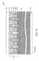
- Bandgaps and lattice constants of common III-V semiconductorsare indicated in FIG. 1 .
- solar cells using a substantially lattice-matched indium gallium phosphide/gallium arsenide/germanium (InGaP/GaAs/Ge) configurationillustrated with dashed lines in FIG. 1 ) formed on Ge substrates achieved the relatively high efficiency of 40.1% in converting sunlight into electricity.
- a solar cell's energy conversion efficiencyis the percentage of power converted (from absorbed light to electrical energy) and collected, when a solar cell is connected to an electrical circuit. This value may be calculated using a ratio of a maximum power point, P m , to the input light irradiance (E, in W/m 2 ) under standard test conditions (STC) and the surface area of the solar cell according to the following equation (A c in m 2 ).
- STCare typically a temperature of 25° C. and an irradiance of 1000 W/m 2 with an air mass of 1.5 (AM1.5) spectrum.
- a three-junction solar cell tailored to increase efficiency without regard for lattice matchingmay employ a configuration other than the aforementioned InGaP/GaAs/Ge configuration, because the bandgaps (shown in Table 1 below) of the lattice-matched materials offer a sub-optimal way of capturing the solar spectrum.
- the theoretical efficiency of a solar cellreaches its maximum when it absorbs each portion of the sun's spectrum with a material that has a bandgap close to the photon energy of the respective portion of the sun's spectrum. In the example of FIG.
- the 1.42 eV bandgap of GaAsis far from the bandgap of approximately 1.1 eV that was determined by modeling to be more suitable as the middle material in a three-junction cell with InGaP and Ge.
- the modelingincluded making a mathematical model of each sub-cell in which the bandgap is one of the variables, setting the currents equal to each other, and running an efficiency optimization algorithm varying each bandgap.
- the different photovoltaic cells that make up a multi-junction cellmay be referred to herein as “sub-cells,” Including photovoltaic sub-cells or solar sub-cells.
- a sub-cellis a fully functional photovoltaic cell, and multiple sub-cells are included in the devices described herein.
- the preferred bandgap of the materials of a sub-cell in a multi-junction solar cellis determined by several factors. If the bandgap in a sub-cell is too high, then photons with an energy below the bandgap may pass through the sub-cell without being absorbed, and the energy of that photon may be lost unless it is absorbed by a lower cell. If the bandgap of a sub-cell is too low, then more photons may be absorbed by that sub-cell, but the higher energy photons may be absorbed inefficiently. A preferred bandgap energy represents a compromise between these two effects.
- FIG. 2shows several possible combinations of materials for a three-junction solar cell with bandgaps that provide a theoretical ability to convert solar energy to electricity with 63.2% efficiency.
- Sisilicon
- ARTaspect ratio trapping
- Ge substratescontribute to the high cost of III-V solar cells: they are smaller and more expensive than Si substrates, and they rule out modern Si processing as a cost-reduction technique. Also, the limited supply of Ge substrates may restrict growth of the market for these devices.
- Misfit dislocationsterminate at the edge of a crystal or at a threading dislocation, i.e., a defect that propagates upward from the interface.
- threading dislocationslie along ⁇ 110> crystal directions; they typically approach the surface at a 45° angle to the substrate. Threading dislocations may degrade device performance and reliability. In solar cells, they may promote recombination of electrons and holes, thereby reducing efficiency.
- the threading dislocation density (TDD) in III-V materials grown directly on Siis typically approximately 10 9 /cm 2 .
- III-V filmstypically range from 450° C. to 800° C.
- the III-V material disposed thereovermay contract more than the Si.
- the substratemay bow in a concave manner, stressing and ultimately cracking the film.
- Graded buffer layersprovide a gradual change in lattice constant from the silicon substrate to the active region of the epitaxial material.
- the typical thickness of the graded buffer layer(10 micrometers ( ⁇ m) of epitaxial growth for a 4% lattice-mismatch) increases the expense of epitaxy and exacerbates cracking.
- Wafer bondinginvolves growing devices on lattice-matched substrates, then lifting off the devices and bonding them to a Si substrate. This approach is relatively costly and may be incompatible with modern Si processing. Furthermore, the difference between the thermal expansion coefficients of the bonded materials and the Si may lead to cracking.
- Selective epitaxy on mesa regionsis a technique that attempts to exploit the glissile behavior of some dislocations.
- the strategyincludes depositing III-V materials in mesa regions 10 to 100 ⁇ m in length, thereby providing a short path along which threading dislocations may glide to the edge of the region and remove themselves from the device.
- structures created by selective epitaxy on mesa regionstypically have a high TDD, above 10 8 /cm 2 , perhaps because selective epitaxy may not remove sessile (immobile) dislocations, which dominate when the lattice-mismatch exceeds 2%.
- embodiments of the inventionfeature a structure including a semiconductor substrate having a top surface and a bottom surface.
- a top insulator layeris disposed proximate the top surface of the substrate and defines a top opening.
- a bottom insulator layeris disposed proximate the bottom surface of the substrate and defines a bottom opening.
- a first crystalline layeris disposed within the top opening, the first crystalline layer being lattice-mismatched to the semiconductor substrate, with a majority of lattice-mismatch defects that arise at a surface of the first crystalline layer nearest the substrate terminating within the top opening.
- a second crystalline layeris disposed within the bottom opening. The second crystalline layer being lattice-mismatched to the semiconductor substrate, and a majority of lattice-mismatch defects arising at a surface of the second crystalline layer nearest the substrate terminate within the bottom opening.
- an embodiment of the inventionfeatures a structure including a substrate, and a first photovoltaic sub-cell formed above the substrate, including a first semiconductor material having a first lattice constant.
- a second photovoltaic sub-cellis formed below the first sub-cell, and includes a second semiconductor material having a second lattice constant different from the first lattice constant.
- a third photovoltaic sub-cellis formed below the second photovoltaic cell and below the substrate, and includes a third semiconductor material having a third lattice constant different from the second lattice constant.
- the first semiconductor materialincludes or consists essentially of a III-V compound
- the first photovoltaic sub-cellcomprises a first photovoltaic junction defined by the III-V compound.
- the second photovoltaic sub-cellmay include a second photovoltaic junction defined in the substrate.
- the first photovoltaic sub-cellincludes a first III-V compound
- the second photovoltaic sub-cellincludes or consists essentially of silicon
- the third photovoltaic cellincludes a second III-V compound.
- the substrateincludes silicon.
- a compositionally graded buffer layermay be disposed between the first and second photovoltaic sub-cells.
- a defect-trapping layermay be disposed between the first and second photovoltaic sub-cells, the defect-trapping layer including (i) a crystalline material comprising defects arising from lattice-mismatch of the crystalline material with an adjacent semiconductor material and (ii) a non-crystalline material, the defects terminating at the non-crystalline material.
- an embodiment of the inventionincludes a structure comprising includes a first photovoltaic sub-cell including a first semiconductor material having a first lattice constant and a first bandgap energy.
- a second photovoltaic sub-cellincludes a second semiconductor material having a second lattice constant different from the first lattice constant and a second bandgap energy lower than the first bandgap energy.
- a defect-trapping layeris disposed between the first and second photovoltaic sub-cells, and has a third bandgap energy higher than the second bandgap energy.
- the defect-trapping layerincludes a crystalline material proximate and in contact with a non-crystalline material, the crystalline material including defects terminating at the non-crystalline material.
- embodiments of the inventioninclude a structure featuring a first defect-trapping layer that includes a first crystalline material proximate and in contact with a first non-crystalline material, with the first crystalline material including defects arising from a lattice-mismatch of the first crystalline material to a first adjacent material, the defects terminating at the first non-crystalline material.
- a second defect-trapping layeris disposed below the first defect-trapping layer.
- the second defect-trapping layerincludes a second crystalline material proximate and in contact with a second non-crystalline material.
- the second crystalline materialincludes defects arising from a lattice-mismatch to a second adjacent material, the defects terminating at the second non-crystalline material.
- the first and second defect-trapping layersmay be disposed on opposite sides of a substrate, the substrate includes the first and second adjacent materials, which may be the same material.
- the first and second defect-trapping layersmay each be disposed above a substrate, which includes the first adjacent material, and the first crystalline material includes the second adjacent material.
- a solar cellis disposed between the first and second defect-trapping layers, below the second defect-trapping layer, or above the first defect-trapping layer.
- a first semiconductor layer having a first lattice constantis disposed above the first defect-trapping layer, and a second semiconductor layer having a second lattice constant different from the first lattice constant is disposed above the second defect-trapping layer.
- the inventionincludes a method of forming a photonic device.
- the methodincludes providing a substrate.
- a first active photonic device layer above the substrate, and a second active photonic device layeris formed below the substrate. Forming each of the first and second active photonic device layers includes epitaxial growth.
- the substratemay include a third photonic device layer.
- the first active photonic device layermay include a first solar cell junction and the second active photonic device layer may include a second solar cell junction.
- an embodiment of the inventionfeatures a multi-junction solar cell device.
- the deviceincludes a first solar cell including a first non-Si photovoltaic junction, a second solar cell disposed below the first solar cell and including a Si photovoltaic junction, and a third solar cell disposed below the second solar cell and second a second non-Si photovoltaic junction.
- embodiments of the inventionfeature a multi-junction solar cell device.
- the deviceincludes a first solar sub-cell having a first energy bandgap. It also includes a second solar sub-cell formed below the first solar sub-cell and having a second energy bandgap greater than the first energy bandgap and approximately equal to 1.1 eV.
- a third solar sub-cellis formed below the second solar cell and has a third energy bandgap greater than the second energy bandgap.
- the first energy bandgapmay be less than 1.1 eV, and preferably less than about 0.8 eV, and the third energy bandgap may be greater than 1.1 eV.
- the second bandgapis generally selected from a range of about 1.0 eV to about 1.2 eV.
- the third energy bandgapis generally greater than about 1.6 eV.
- FIG. 1is a graph illustrating the bandgaps and lattice constants of common lattice-matched III-V semiconductor materials
- FIG. 2is a graph illustrating selection of materials for a non-lattice-matched three-junction solar cell with bandgaps that provide a theoretical ability to convert solar energy to electricity with 63.2% efficiency;
- FIG. 3is a schematic diagram illustrating the basic principles of ART
- FIGS. 4 and 5are schematic diagrams illustrating facet formation adjacent a dielectric sidewall
- FIG. 6is a schematic diagram illustrating growth planes of a material formed by employing ART
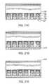
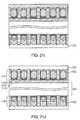
- FIGS. 7-10are schematic diagrams illustrating various samples formed by employing ART
- FIG. 11is a schematic diagram illustrating a three-junction solar-cell structure
- FIG. 12is a schematic diagram illustrating an ART structure for growing InGaP
- FIG. 13is a schematic diagram illustrating various growth modes of lattice-mismatched materials
- FIG. 14is a schematic diagram illustrating growth of wide bandgap InP below InGaAs in an ART region
- FIG. 15is a schematic diagram illustrating a structure for a single-junction InGaP solar cell
- FIG. 16is a schematic diagram illustrating an architecture for a single junction InGaAs solar cell
- FIG. 17is a schematic diagram illustrating a dual-junction InGaP/Si solar cell
- FIG. 18is a schematic diagram illustrating a dual-junction InGaAs/Si solar cell
- FIG. 19is a schematic diagram illustrating an alternative architecture for a single junction InGaAs solar cell utilizing a coalesced material
- FIG. 20is a schematic diagram illustrating an alternative embodiment of a InGaP/Si/InGaAs cell with a coalesced buffer region;
- FIGS. 21 a - 21 jare a series of schematic diagrams illustrating the fabrication of a three-junction InGaP/Si/InGaAs solar cell;
- FIG. 22is a schematic diagram illustrating a five-junction InGaP/GaAs/Si/GaAsSb/InGaAs solar cell;
- FIG. 23is a schematic diagram illustrating a three-junction InGaP/GaAs/InGaAs solar cell disposed over a Si substrate;
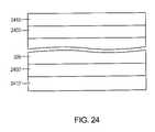
- FIG. 24is a schematic diagram illustrating a three-junction InGaP/Si/InGaAs solar cell incorporating InGaP graded buffer layers on both sides of a Si substrate;
- FIGS. 25 a - 25 bare schematic diagrams illustrating the use of wafer bonding or layer transfer to create a three-junction InGaP/Si Ge solar cell.
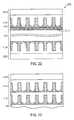
- FIGS. 26 a - 26 fare a series of schematic diagrams illustrating an alternative method for forming an ART structure.
- solar cellAs used herein, the terms “solar cell,” “photovoltaic cell,” and “photovoltaic sub-cell” each denote a structure having a photovoltaic junction, e.g., a p-n junction.
- a “photonic device layer”refers to a photoactive device, such as a solar cell.
- ARTenables solar-cell designers to select junction materials on the basis of their bandgaps without being constrained by their lattice constants. It also enables solar cell manufacturers to take advantage of inexpensive Si substrates and modern Si processing technologies. Multi-junction solar cells fabricated on Si substrates by ART also offer good mechanical strength, light weight, and superior heat dissipation in comparison to Ge substrates. The superior heat dissipation may be especially important in concentrator applications, since solar cells generally work less efficiently at elevated temperatures.
- ARTsubstantially eliminates problems from threading dislocations arising from a mismatch between the lattice constants of a film and an underlying substrate. It reduces stress due to the mismatch in thermal expansion coefficients, employs standard equipment, and does not require prohibitively expensive processes.
- an ART structuremay be formed in accordance with the following steps.
- a semiconductor substrate 300i.e., a semiconductor wafer, is provided.
- the semiconductor substrate 300may include a semiconductor material and may be, for example, a bulk silicon wafer, or a bulk germanium wafer.
- the substrate 300may include or consist essentially of a first semiconductor material, such as a group IV element, e.g., germanium or silicon.
- the substrate 300includes or consists essentially of (300) silicon.
- a dielectric layer 310including a dielectric material, i.e., a non-crystalline material such as SiO 2 is formed over the semiconductor substrate 300 .
- SiO 2is just one example of a dielectric material, and those of skill in the art may substitute other materials, such as SiN x , as appropriate, for example, to reduce recombination effects.
- the dielectric layer 310may be formed by a method known to one of skill in the art, e.g., thermal oxidation or plasma-enhanced chemical vapor deposition (PECVD) in a suitable system, such as the CENTURA ULTIMA manufactured by Applied Materials, based in Santa Clara, Calif.
- PECVDplasma-enhanced chemical vapor deposition
- the dielectric layermay have a thickness t 1 corresponding to a desired height of crystalline material to be deposited in an opening formed through the dielectric layer.
- the thickness t 1 of the dielectric layer 310may range from, e.g., 25 nm to 20 ⁇ m.
- a plurality of narrow, sub-micron-width openingsare defined in the dielectric layer 310 by conventional lithography and reactive ion etching, with the openings having dielectric sidewalls 325 .
- lithography and reactive ion etchingare defined in the dielectric layer 310 by conventional lithography and reactive ion etching, with the openings having dielectric sidewalls 325 .
- additional stepssuch as treating SiO 2 with a hydrogen plasma to passivate the sidewalls of the trench.
- a lattice-mismatched material 330is selectively grown within the opening 320 .
- the lattice-mismatched materialmay be, e.g., a semiconductor or Ge, grown in the opening by, e.g., selective epitaxy.
- the threading dislocations in the lattice-mismatched materialtypically slope towards the sidewalls of the opening and terminate when they reach the dielectric material, e.g., SiO 2 . Accordingly, a region of the epitaxial material near the top of the trench is preferably substantially free of dislocations.
- An ART structuremay be used as a defect-trapping layer in the solar cells discussed below.
- the ART structureincludes (i) a crystalline material including defects arising from lattice-mismatch of the crystalline material with an adjacent semiconductor material and (ii) a non-crystalline material, with the defects terminating at the non-crystalline material.
- the bond between a germanium atom and an oxygen atomrequires higher energy than the bond between two Ge atoms.
- the Ge—O bondis therefore less favorable, and, accordingly, is less likely to form. Accordingly, under typical growth conditions, the Ge atoms form a facet 400 , typically a ⁇ 111 ⁇ or ⁇ 113 ⁇ crystal plane, as shown in FIG. 4 .
- two crystal planese.g., ⁇ 111 ⁇ plane 500 , and ⁇ 100 ⁇ plane 500 ′ may grow simultaneously.
- the growth rate of the two planesmay be different. For example, in Ge the ⁇ 100 ⁇ plane grows faster than the ⁇ 111 ⁇ plane, as shown in FIG. 5 . Eventually the fast growth plane disappears because the crystal growth in the direction of the fast plane is limited by the growth rate of the slow growth plane, as also shown in FIG. 5 .
- thin regions of a marker material defining a marker layer 600may be interposed within the lattice-mismatched material 330 .
- thin Si—Ge regions, or “marker layers”may be interposed within a Ge matrix to provide contrast in TEM images.
- These marker layers 600appear as black chevrons in the schematic representation of a TEM micrograph in FIG. 6 .
- the Gegrows with a ⁇ 100 ⁇ crystal orientation in the lowest sector of the figure (below the letter A). Above that region, the angled black Si—Ge marker layers show that the Ge has transitioned to ⁇ 111 ⁇ growth planes or facets.
- the following behavior of a threading dislocation 610is observed:
- the crystal boundaryWhen the threading dislocation reaches a facet boundary, the crystal boundary typically redirects it in a direction perpendicular to the facet.
- the facetinclines the threading dislocation towards the sidewalls. All threading dislocations in a material having facets non-parallel to an underlying substrate, therefore, typically intersect a sidewall, if the sidewall is sufficiently high.
- the aspect ratio of the trenchi.e., the ratio of its height to its width, is preferably greater than about 1.
- the sidewallspreferably trap the dislocations, leaving a defect-free region of epitaxial material at the top of the trench. This approach substantially eliminates substrate interface defects in one lithography and one selective epitaxial growth step.
- FIG. 7a schematic diagram of a TEM image illustrates that Ge deposited in openings 320 , e.g., trenches 200 nm wide, may be free of defects 610 above a trapping region. Top-view (“plan-view”) TEM images of the material were then captured.
- FIG. 8a schematic diagram based on a TEM micrograph, illustrates the trapping of threading dislocations by SiO 2 sidewalls 325 , with the dislocations terminating at the sidewalls in the lower portion of the ART regions.
- a lower region of Ge containing the dislocationsmay be removed.
- the upper regionafter removal of the substrate 300 and dislocation 610 regions, may be free of defects.
- the Ge in the upper regionsmay contain no threading dislocations due to lattice-mismatch, no stacking faults, no twins (two-dimensional lattice imperfections), and no cracks.
- FIG. 10illustrates trenches filled with a crystalline material, e.g., GaAs, between dielectric, e.g., SiO 2 , sidewalls on substrate 300 , e.g., Si.
- the threading dislocations 610slant towards the sidewall 325 near the bottom of the trenches.
- the GaAsis free of defects above the dashed line.
- the use of ARThas been confirmed for the deposition of high-quality III-V materials on Si substrates, thereby confirming its viability for creating high-efficiency, low-cost multi-junction solar cells on Si substrates.
- the lattice and bandgap parameters of an embodiment of a solar cell with three junctions made from In 0.5 Ga 0.5 P (1.86 eV), Si (1.15 eV), and In 0.7 Ga 0.3 As (0.61 eV)are illustrated.
- This solar cellhas a theoretical maximum efficiency of 63.2%.
- This figureindicates that a device using InGaP material with 50% indium and 50% gallium is shown, but other concentrations of indium and gallium may be used to tune the bandgap and lattice constant of the material to improve the solar cell performance.
- the bandgaps for 70% indium and 30% galliumare shown, but other fractions of indium and gallium may be used in the InGaAs layer to tune the bandgap and lattice constant for improved performance.
- FIG. 11shows a three-junction solar-cell structure 1100 including a top ART region 1110 including InGaP regions with p-n junctions formed on the top of a silicon substrate 300 by ART, a p-n junction 1120 within the silicon substrate, and a bottom ART region 1130 including InGaAs regions with p-n junctions defined on the bottom surface of the silicon substrate by ART.
- the structuremay incorporate tunnel junctions to make electrical contact between the three sub-cells, i.e., the top ART region, the substrate, and the bottom ART region.
- the top ART region 1110may function as a first defect-trapping layer including a first crystalline material 330 (e.g., InGaP) proximate and in contact with a first non-crystalline material 310 (e.g., SiO 2 ).
- the first crystalline materialincludes defects 610 arising from a lattice-mismatch of the first crystalline material to a first adjacent material (e.g., the Si substrate 300 ); the defects terminate at the first non-crystalline material 310 .
- the top ART region 1110may include a wetting layer 1140 of, e.g., p + GaAs.
- the composition of the wetting layer 1140is selected such that it forms a high-quality, continuous layer over the underlying material, e.g., Si, to allow the subsequent growth of the first crystalline material, e.g., InGaP.
- the top ART regionmay also include a base 1145 of, e.g., p InGaP, and an emitter 1150 of, e.g., n + InGaP. InGaP may be selected because it has an appropriate bandgap.
- a photovoltaic junction 1152is defined by the interface between the base 1145 and the emitter 1150 .
- the InGaP material and In and Ga fractionsare chosen so that the material has a bandgap of about 1.86 eV.
- This bandgapis chosen so that the top sub-cell absorbs high energy photons efficiently but allows lower energy photons to pass through undisturbed.
- the emitteris highly doped n-type to provide low resistance from the InGaP to the top contact metal.
- the baseis lightly doped p-type so that the InGaP has a high minority-carrier lifetime, which is preferred so that electron-hole pairs do not recombine before they are separated by the p/n junction.
- the top ART regionmay have a thickness of e.g., about 1 to 5 ⁇ m.
- a top contact layer 1155e.g., a conductive material such as NiAu, may be disposed over the top ART region.
- the bottom ART region 1130may function as a second defect-trapping layer disposed below the first defect-trapping layer; the second defect-trapping layer includes a second crystalline material 330 ′ (e.g., InGaAs) proximate and in contact with a second non-crystalline material 310 ′ (e.g., SiO 2 ).
- the second crystalline materialincludes defects 610 ′ arising from a lattice-mismatch to a second adjacent material (e.g., the Si substrate); the defects terminate at the second non-crystalline material 310 ′.
- the bottom ART region 1130may include a wetting layer 1140 ′ of, e.g., n + GaAs, a bottom trapping region 1160 of, e.g., n + InP, an emitter 1150 ′ of, e.g., n + InGaAs, and a base 1145 ′ of p InGaAs, with a photovoltaic junction 1152 ′ defined by an interface between the emitter 1150 ′ of, e.g., n + InGaAs and the base 1145 ′ of, e.g., p InGaAs.
- the bottom ART region 1130may have a thickness of e.g., about 1 to 5 ⁇ m.
- a bottom contact layer 1155 ′e.g., a conductive material such as NiAu, may be disposed over the bottom ART region.
- a solar celli.e., p-n junction 1120
- the p-n junctionmay be defined, e.g., by an emitter 1167 of n + Si formed by, for example, ion implantation, in a p-type Si substrate, with the remainder of the substrate defining a base 1168 , the p-n junction 1120 being disposed between the emitter and the base.
- a tunnel junction 1170may be formed between the substrate 300 and the top ART region, and another tunnel junction 1170 ′ may be formed between the substrate and the bottom ART region.
- a tunnel junctionis a very highly doped p + /n + diode. The doping is sufficiently high for current to tunnel between the p + and n + layers, with the tunnel junction forming a low resistance contact between two adjacent layers. In other words, the doping is sufficiently high such that the p + /n + junction depletion region is small enough for tunneling to occur when the top ART region is exposed to light and, therefore, current flows through the top ART region. The current forward biases the tunnel junction.
- the tunnel junctionsmay be formed in III-V materials formed above and below the semiconductor substrate 300 .
- tunnel junctions 1170 , 1170 ′may be defined in the top and bottom portions of a Si substrate 300 . Then the doping in the silicon starting from the top of the silicon substrate may be as follows:
- a structuremay include additional solar cells disposed, e.g., below the second defect-trapping layer or above the first defect-trapping layer. In some embodiments, both the first and the second defect-trapping layers are disposed above a substrate.
- a large array (500,000 on a 12-inch substrate) of trenches 300 nm to 500 nm widecovers the surface of each die on a Si substrate.
- the trench widthcan vary over a broader range, such as from 180 nm to 5 ⁇ m.
- the distance between the trenchesmay be about 150 nm, below the wavelength of almost all of the solar radiation. This configuration may prevent solar radiation from passing between the trenches; therefore, the cell may absorb almost all of the incident light. While the 150 nm spacing is preferable for some criteria, the spacing may be substantially adjusted, based on application and/or material requirements.
- the ART based 3-junction solar-cell structure shown in FIG. 11operates as follows.
- Dislocationsmay cause absorption of sub-bandgap photons, but this sub-bandgap absorption does not significantly affect the performance of an ART-based cell.
- the absorption coefficient of InP and GaAs regions grown on siliconis approximately 5 ⁇ 10 3 /cm for photons with energies between 0 and 0.5 eV below the bandgap.
- the transmission through the trapping regionsis expected to be about 95%.
- the InGaPabsorbs about 33% of the photons before any of them enter a trapping region. The remaining 67% of the photons enter the trapping regions in the InGaP cell.
- the trapping regions in the InGaP cellnominally absorb about 5% of that 67%, or about 3.3% of all the incident solar photons.
- the remaining photonsthen pass through the silicon cell before they enter the trapping region in the InGaAs cell.
- the two upper (InGaP and Si) cellshave absorbed about 67% of all the incident solar photons. Only 33% of the total incident solar photons reach the trapping region in the InGaAs cell.
- the trapping regionsnominally absorb about 5% of that 33%, or about 1.7% of all the incident solar photons.
- ARTin solar cells may reduce the detrimental effect of dislocations.
- a dislocationcan induce recombination over a relatively long distance, e.g., up to about 10 ⁇ m.
- the use of ART to make solar cells in trenches 300 to 500 nm widereduces the sphere of influence of a defect significantly in comparison to a defect's influence in a bulk material or a film, since a dislocation cannot induce recombination in an adjacent trench.
- InGaP and InGaAs on silicon using ARTis an important part of the fabrication process used to create the triple junction cell shown in FIG. 11 .
- Techniques for forming InGaP and InGaAs on silicon using ARTare now described in greater detail.
- FIG. 12illustrates an embodiment of an ART structure for growing InGaP.
- a suitable Si substrate 300may be obtained, for example, from ATDF, a subsidiary of SEMATECH.
- p-type Si (001) substratesare offcut by 6° to avoid anti-phase domain boundaries.
- a relatively thick dielectric layer 310e.g., a thermal oxide having a thickness of 1 to 1.5 ⁇ m, is formed on the substrate.
- fluorocarbon residuemay be removed from the substrate surface by an oxygen plasma ashing step (800 W at 1.2 Torr for 30 minutes in an oxygen plasma asher.
- the residue removalmay be performed in, e.g., an ASPEN STRIP II system manufactured by Mattson Technology, Inc., based in Fremont, Calif.
- the patterned substrateis cleaned, for example in Piranha, SC2, and dilute HF solutions sequentially.
- Epitaxial lattice-mismatched material 330is selectively formed in the trench by, e.g., metal-organic chemical vapor deposition (MOCVD).
- MOCVDmetal-organic chemical vapor deposition
- the epitaxial lattice-mismatched material 330may include InGaP disposed over a wetting layer 1140 of GaAs.
- FIG. 13shows three possible growth modes of lattice-mismatched material 330 .
- FMFrank-Van der Merwe
- VWVolmer-Weber
- SKStranski-Krastanov
- InGaPtends to grow on Si in a non-planar mode, i.e., in either the second (VW) or third (SK) mode.
- Non-planar growthi.e., VW or SK mode
- This issueis addressed by depositing a wetting layer 1140 of, e.g., GaAs directly onto the Si substrate before depositing the InGaP.
- the GaAswill grow in 2D layers on Si, and InGaP will grow in 2D layers on GaAs.
- Table 2shows an exemplary set of conditions that may be adjusted for growing GaAs and InGaP.
- V-III Rate Material Gases Gas(° C.) (Torr) Ratio (nm/min) GaAs Triethyl H 2 330-400 50-100 50-100 6 Gallium (TEG), Arsine InGaP Trimethyl H 2 650-720 50-100 200-300 30 Indium (TMI), TMG, Phosphine
- the V/III ratiois defined as the ratio between the flow rate of a group V element in the group V precursor to the flow rate of the group III element in the group III precursor, and may be calculated as (V precursor flow rate/III precursor flow rate)*(fraction of V element in V precursor/fraction of III element in III precursor).
- the V-III ratiois equal to the number of group V atoms/second that enter a processing chamber divided by the number of group III atoms/second that enter the processing chamber.
- Growth conditionsmay be adjusted in a variety of ways, such as, for example:
- a high-bandgap InP trapping regionmay be interposed between the Si substrate and the InGaAs to avoid photon absorption in the trapping region of the lowest solar cell.
- the bandgap of the trapping regionis preferably significantly higher than the bandgap of the sub-cell below the trapping region. If photons are absorbed in the trapping region, they do not convert into electrical energy because they recombine in the dislocations in the trapping region. If the trapping region bandgap is large, photons tend to pass through it and are absorbed efficiently by an underlying the sub-cell.
- FIG. 14illustrates a structure in which a first crystalline material 330 , e.g., wide bandgap InP, is formed over a GaAs wetting layer 1140 disposed in a trench 320 . Subsequently, another crystalline material 1400 , e.g., InGaAs, is formed over the first crystalline material, e.g., InP. InP is used to trap defects, and has a large bandgap, so light is not absorbed in it. The InGaAs functions as a solar cell. Table 3 sets forth an exemplary set of conditions that may be adjusted for growing InP and InGaAs.
- a first crystalline material 330e.g., wide bandgap InP
- FIG. 15shows an exemplary architecture for a single-junction InGaP solar cell 1500 .
- FIG. 15 and other drawings of solar cells hereinare schematics, rather than precise drawings. They omit, for example, contact doping regions, window layers, and back surface field layers, whose presence would be readily apparent to those of skill in the art.
- the single-junction solar cell 1500includes a top ART region 1110 , as discussed with reference to FIG. 11 , and p + GaAs wetting layer 1140 disposed in a trench 320 over a p + Si substrate 300 .
- a base layer 1145 of p InGaPis disposed over the wetting layer, and an emitter layer 1150 of n + InGaP is disposed over the base layer, defining a photovoltaic junction 1152 therebetween.
- the top ART regionmay have a thickness of e.g., about 1 to 5 ⁇ m.
- a top contact layer 1155e.g., a conductive material such as NiAu, may be disposed over the top ART region.
- a bottom contact layer 1155 ′may be formed on the side of the Si substrate opposite the top ART region.
- the metals for the top and bottom contact layersare preferably selected to provide a low contact resistance with the adjacent semiconductor material.
- aluminumprovides a low contact resistance with doped silicon but not with III-V materials.
- aluminumis preferably used as a contact layer adjacent to doped silicon.
- the Si substrate 300may be doped p + and have a thickness of about 200 to 700 ⁇ m, with a preferred thickness of about 300 ⁇ m. Sunlight may impinge on the single-junction solar cell 1500 through the top contact layer 1155 .
- Trench widths, the layer thicknesses, and the doping levelsmay be varied to increase efficiency.
- the InGaP thicknessis between about 1 to 1.5 ⁇ m.
- FIG. 16shows an architecture for a single-junction InGaAs solar cell 1600 .
- trench widths, layer thicknesses and doping levelsmay be tailored to increase efficiency.
- the single-junction InGaAs solar cell 1600includes a bottom ART region 1130 , as discussed with reference to FIG. 11 , formed on an n + Si substrate 300 .
- the bottom ART region 1130may include a wetting layer 1140 ′ of, e.g., n + GaAs, a bottom trapping region 1160 of, e.g., n + InP, an emitter 1150 ′ of, e.g., n + InGaAs, and abase 1145 ′ of p InGaAs, with a photovoltaic junction 1152 ′ defined by an interface between the emitter 1150 ′ and base 1145 ′.
- the bottom ART region 1130may have a thickness of e.g., about 1 to 5 ⁇ m.
- a bottom contact layer 1155 ′e.g., a conductive material such as NiAu, may be disposed over the bottom ART region.
- a top contact layer 1155e.g., an Al layer, may be formed on the side of the Si substrate opposite the bottom ART region. Sunlight may impinge on the single-junction solar cell 1600 through the top contact layer 1155 .
- the InGaAs thicknessis between about 1 to 3 ⁇ m.
- the bottom ART region 1130may have a thickness of 1-5 ⁇ m.
- the substratemay have a thickness of about 300 ⁇ m.
- FIG. 17illustrates an embodiment of a dual-junction InGaP/Si cell 1700
- FIG. 18illustrates an embodiment of a dual-junction InGaAs/Si cell 1800
- the dual-junction InGaP/Si solar cell 1700includes a top ART region 1110 as described with reference to FIG. 11 and having a first photovoltaic junction 1152 , disposed over a substrate 300 defining a second junction.
- the substratemay be p-type Si, having a thickness of about 300 ⁇ m.
- An emitter region 1705 of n + Simay be formed in the substrate 300 by ion implantation.
- a base 1710may be defined by the remainder of the substrate 300 .
- a second photovoltaic junction 1720is formed between the emitter 1705 and the base 1710 .
- a tunnel junction 1170may be disposed between the top ART region 1110 and the emitter 1705 .
- a bottom metal layer 1155 ′e.g., Al, is formed on a backside of the substrate 300 .
- the top ART region 1110may be formed adjacent to the emitter 1705 .
- the dual junction solar cell 1800 of FIG. 18includes a first photovoltaic cell including a first semiconductor material having a first lattice constant and a first bandgap energy, e.g., Si.
- the first photovoltaic cellcorresponds to the Si substrate 300 , which includes an emitter 1705 of n + Si, a base 1710 of p-type Si, and a photovoltaic junction 1720 .
- a second photovoltaic cellincludes a second semiconductor material having a second lattice constant different from the first lattice constant and a second bandgap energy lower than the first bandgap energy.
- the second photovoltaic cellmay be formed adjacent to the base 1710 in, e.g., InGaAs, in a bottom ART region 1130 , as described with reference to FIG. 11 .
- the second photovoltaic cellmay include an emitter 1150 ′ of n + InGaAs and a base 1145 ′ of p InGaAs, with a junction 1152 ′ formed at the interface between the emitter and the base.
- a defect-trapping layer 1160is disposed between the first and second photovoltaic cells.
- the defect-trapping layerincludes, e.g., n + InP, a material having a third bandgap energy higher than the second bandgap energy.
- the defect-trapping layerincludes a crystalline material (e.g., InP) proximate a non-crystalline material 310 (e.g., SiO 2 ), with the crystalline material including defects terminating at the non-crystalline material.
- a solar cell architecturemay include a film that is grown until it overflows the trench 320 , as illustrated in FIG. 19 , to create an ART buffer layer 1900 .
- the illustrated embodimentdepicts a single-junction ART solar cell 1905 incorporating the ART buffer layer 1900 . Adjacent discrete regions of lattice-mismatched material coalesce to form a single continuous film, i.e., the ART buffer layer 1900 .
- a solar cell p-n junctionis then grown on the buffer layer.
- the solar cell p-n junctionmay include a base 1910 and an emitter 1920 , with a metal 1930 disposed thereover.
- the total thickness of the emitter, base, and dielectric layermay be about 1 to 5 ⁇ m.
- the structuremay be formed on a substrate 300 , e.g., Si, having a thickness of approximately 300 ⁇ m.
- a substrate 300e.g., Si
- sidewall recombinationdoes not diminish the solar cell performance because the active regions of the solar cell do not reside in the trench 320 .
- FIG. 19also illustrates a coalescence defect 1940 , the vertical dotted line emerging from the top of a SiO 2 sidewall 325 .
- These types of defectsmay appear in a selectively grown epitaxial film above a certain percentage of the SiO 2 pedestals, which may vary as a function of deposition conditions. Exemplary methods to reduce the density of these coalescence defects include:
- the ART buffer layeris formed from the primary solar cell material; e.g., InGaP on the top and InGaAs on the bottom.
- CMPchemical-mechanical-polishing
- FIG. 20shows an alternative embodiment that uses a coalesced buffer region to form a three junction InGaP/Si/InGaAs cell 2000 .
- a single junction ART solar cell 1905incorporates a ART buffer layer 1900 that includes p InGaP disposed over a wetting layer 1140 of p + GaAs formed in an opening defined in a dielectric material 310 .
- a base 1910 of, e.g., p + InGaPis disposed over the buffer layer 1900
- an emitter 1920 of e.g., n + InGaPis disposed over the base, with a photovoltaic junction 2020 being formed at the interface between the emitter layer 1920 and the base 1910 .
- the single junction ART solar cell 1905may have a thickness of e.g., 1 to 5 ⁇ m.
- a metal 1930 of, e.g., NiAu,is disposed over the single junction ART solar cell 1905 .
- the single junction ART solar cell 1905is formed over a substrate 300 of, e.g., p-type Si, having a thickness of about 700 ⁇ m.
- An emitter region 2030 of, e.g., n + Si,is defined in the substrate, with the remainder of the p-type Si substrate defining a base 2040 .
- a second photovoltaic junction 2020 ′is defined by an interface between the emitter 2030 and the base 2040 .
- Tunnel junctions 1170 , 1170 ′are formed on the top and bottom surfaces of the semiconductor substrate 300 .
- a second single-junction ART solar cell 1905 ′is disposed over a backside of the substrate 300 , adjacent the base 2040 .
- the cell 1905 ′includes a third photovoltaic junction 2020 ′, disposed between an emitter 1920 ′ of n + InGaAs and a base 1910 ′ of p-type InGaAs.
- An ART buffer layer 1900 ′may be formed over a trapping layer 1160 ′ of n+InP that is disposed over a wetting layer 1140 ′ of n + GaAs.
- an exemplary process for fabricating a three-junction InGaP/Si/InGaAs solar cellincludes the following steps:
- the resulting structurehas a top ART region 1110 , i.e., a first solar cell or photovoltaic cell, disposed above the substrate 300 .
- the first solar cellincludes a first semiconductor material having a first lattice constant, i.e., the first crystalline layer.
- the first semiconductor materialincludes a first III-V compound, and the first solar cell has a first photovoltaic junction 1152 defined by the III-V compound.
- a second solar cell or photovoltaic cellis disposed below the first solar cell, e.g., defined in the substrate 300 .
- the material of the second solar celle.g., silicon, has a second lattice constant mismatched with respect to the first semiconductor material.
- the second solar cellincludes an emitter 1705 and a base 1710 , with a second photovoltaic junction 2110 defined therebetween.
- a bottom ART region 1130i.e., a third solar cell or photovoltaic cell, is disposed below the second solar cell and below the substrate.
- the third solar cellincludes the second semiconductor material that is lattice-mismatched to the material of the second solar cell, e.g., a second III-V compound, and a photovoltaic junction 1152 ′.
- the first solar cellhas a first energy bandgap, e.g., less than 1.1 eV; in some embodiments, the first energy bandgap is less than about 0.8 eV.
- the second solar cellis disposed below the first solar cell and has a second energy bandgap greater than the first energy bandgap and approximately equal to a bandgap of silicon, i.e., 1.1 eV.
- the third solar cellis disposed below the second solar cell and has a third energy greater than the second energy bandgap, e.g., greater than 1.1 eV. In some embodiments, the third energy bandgap is greater than about 1.6 eV.
- FIG. 22illustrates a five-junction InGaP/GaAs/Si/GaAsSb/InGaAs solar cell 2200 .
- this embodimentuses ART on both sides of a Si substrate 300 that has a photovoltaic junction 2110 defined therein. ART is used to trap defects to facilitate forming two solar cells, i.e., a top ART cell 1110 containing GaAs and a bottom ART cell 1130 containing GaAsSb, above the top and bottom surfaces of the Si substrate, respectively.
- a fourth photovoltaic cell 2210e.g., an InGaP cell
- a fifth photovoltaic cell 2220is formed over the GaAsSb cell.
- the crystal lattices for these latter cell pairsare substantially matched to adjacent materials and thereby avoid lattice-mismatch defects.
- FIG. 23illustrates an embodiment in which ART is first used to form a first top ART region 1110 that traps defects arising from lattice-mismatch for an InGaAs solar cell, which has a nominal bandgap of about 0.7 eV, grown above a silicon substrate 300 . Then a second top ART region 1110 ′ is formed over the first top ART region.
- the second top ART regionincludes a GaAs solar cell with a nominal bandgap of about 1.4 eV.
- a third solar cell 2300including, e.g., n- and p-type InGaP, which has a nominal bandgap of about 1.8 eV, is grown above the second top ART region 1110 ′, i.e., over the GaAs cell.
- FIG. 24shows the use of compositionally graded top and bottom buffer layers 2400 , 2400 ′, e.g., InGaP graded buffer layers formed on both sides of a substrate 300 , e.g., a Si substrate, to facilitate a three-junction InGaP/Si/InGaAs solar cell.
- a substrate 300e.g., a Si substrate
- the graded buffer layers 2400 , 2400 ′each start with GaP formed adjacent the Si substrate (because GaP has a lattice constant that approximately matches that of Si).
- the graded buffer layer 2400On a top side of the Si substrate, the graded buffer layer 2400 includes GaP and is graded to a layer of (approximately) In 0.5 Ga 0.5 P, and on a bottom side, the graded buffer layer 2400 ′ includes GaP graded to an In x Ga 1-x P layer that has a lattice constant matched, at least approximately, to the lattice constant of InGaAs.
- the graded buffer layers 2400 , 2400 ′are disposed between the first (InGaP top photovoltaic cell 2410 ) and second (Si substrate 300 photovoltaic cell) photovoltaic cells, and the second (Si substrate 300 ) and third (InGaAs bottom photovoltaic cell 2410 ′) photovoltaic cells, respectively.
- Those of skill in the artunderstand the criteria for the selection of materials and other parameters such as thicknesses and growth conditions for the graded buffer layers.
- FIGS. 25 a and 25 billustrate an embodiment that uses wafer bonding or layer transfer to create a three-junction InGaP/Si/Ge solar cell 2500 .
- a single-junction Si solar cell 2510i.e., a first active photonic device layer
- a single-junction Ge solar cell 2520i.e., a second active photonic device layer
- An InGaP solar cell 2530is formed on a GaAs substrate 2540 . Wafer bonding techniques are then used to combine the Si, Ge, and InGaP solar cells 2510 , 2520 , and 2530 into a multi-junction solar cell 2500 , with the GaAs substrate 2540 being removed, for example, by wet etching.
- the first active photonic device layermay be formed in InGaP 2530 and bonded to a top surface of the Si substrate 2510 (including a solar cell).
- a second active photonic device layermaybe formed in Ge 2520 and bonded to a bottom surface of the Si substrate 2510 .
- a third active photonic device layermay be defined by the Si substrate 2510 .
- FIG. 25 billustrates an embodiment with a current path that flows from the InGaP cell 2530 through the Si cell 2510 and into the Ge cell 2520 .
- a dielectric layermay be included between each of the cells, in which case separate electrodes are used for each of the three cells.
- an ART regionmay be formed in, rather than over, a substrate.
- An exemplary processis illustrated in FIGS. 26 a - 26 f .
- a substrate 300e.g., a Si wafer, is provided.
- a masking layer 2600is formed over the substrate 300 .
- the masking layer 2600may include a thin layer of silicon dioxide 2610 and a thicker layer of silicon nitride 2620 disposed thereover.
- the silicon dioxide layermay about 100 nm thick and the silicon nitride layer may be about 1000 nm.
- the silicon dioxide layeris interposed between the silicon nitride layer and the substrate to reduce cracking of the nitride layer.
- the masking layeris patterned by a photolithographic patterning step, and openings 2630 are dry etched through the masking layer 2600 and into the substrate 300 .
- the openings 2630may be, e.g., trenches.
- the trench widthmay range from 20 nm to 20 ⁇ m and the depth is selected such that the trench aspect ratio (the ratio of the depth to the width) is ⁇ 1.
- a second silicon dioxide layer 2640is conformally deposited over the masking layer 2600 and along the sidewalls of the openings 2630 or grown along the sidewalls of the openings 2630 .
- a dry etch of the second silicon dioxide layer 2640is performed, removing the second dioxide layer 2640 from the silicon nitride 2620 and from the bottom portions 2650 of the openings, and leaving the second silicon dioxide layer 2640 on the sidewalls 2660 of the openings.
- a thin layer, about between 10 and 100 nm, optimally 25 nm, of silicon dioxidemay be grown over the silicon dioxide portions 2620 and the exposed bottom portions of the openings, and subsequently removed by a dip in HF. This thin silicon dioxide layer is grown and stripped to clean the surface of the bottom of the trench, thereby removing damage and carbon compounds left over after the trench dry etch.
- the resulting structureincludes openings 2630 defined in the substrate 300 , with silicon dioxide layers 2610 , 2640 disposed over the sidewalls of the openings and over the top surface of the substrate 300 .
- This configurationprovides an exposed crystalline surface suitable for epitaxial growth (i.e., the exposed substrate material in the bottom portions of the openings) and openings lined with a dielectric material, suitable for trapping defects by ART in lattice-mismatched crystalline material formed in the openings.
- lattice-mismatched material 330may be formed in the openings, and used to form the solar-cell structures described above.
Landscapes
- Engineering & Computer Science (AREA)
- Manufacturing & Machinery (AREA)
- Physics & Mathematics (AREA)
- Condensed Matter Physics & Semiconductors (AREA)
- General Physics & Mathematics (AREA)
- Computer Hardware Design (AREA)
- Microelectronics & Electronic Packaging (AREA)
- Power Engineering (AREA)
- Chemical & Material Sciences (AREA)
- Crystallography & Structural Chemistry (AREA)
- Materials Engineering (AREA)
- Photovoltaic Devices (AREA)
- Sustainable Energy (AREA)
- Life Sciences & Earth Sciences (AREA)
Abstract
Description
| TABLE 1 |
| Bandgaps of In0.5Ga0.5P, GaAs, and Ge |
| Material | Bandgap (eV) | ||
| In0.5Ga0.5P | 1.86 | ||
| GaAs | 1.42 | ||
| Ge | 0.66 | ||
- It rises vertically from the
substrate 300 through the region with the {100}crystal orientation 500′, toward the letter A. - At point A, the threading dislocation intersects the region with the {111}
crystal orientation 500. The facets of the crystal direct the threading dislocation to a direction normal to the {111} facet, toward the sidewall. - The threading dislocation reaches the SiO2sidewall and terminates.
- It rises vertically from the
- The stresses are small because the epitaxial layers are thin.
- The material may elastically accommodate stresses arising from thermal-expansion mismatch because the trenches are relatively narrow, in contrast to very wide trenches, in which material behavior may approximate that of a bulk film.
- The dielectric material of the sidewall, e.g., SiO2, tends to be more compliant than the semiconductor materials, and may serve as an expansion joint, stretching to accommodate the stress.
| p++ (tunnel junction) | 1170 | ||
| n++ (tunnel junction) | 1170 | ||
| n+(emitter) | 1167 | ||
| p (base) | 1168 | ||
| p++ (tunnel junction) | 1170′ | ||
| n++ (tunnel junction) | 1170′ | ||
- Sunlight first strikes the
InGaP material 330 of thetop ART cell 1110. InGaP absorbs photons with an energy of 1.82 eV or higher. Photons with an energy below 1.82 eV pass through the InGaP and enter theSi Substrate 300. - The photons that pass through the InGaP enter the top defect-trapping
region 1165. Preferably, absorption in this region is avoided or reduced because photogenerated carriers may recombine at the threadingdislocations 610. Because most of the top trapping region is created from InGaP, the trapping region will be transparent to the photons not absorbed by the region of InGaP above. While awetting layer 1140 of GaAs is provided to facilitate two-dimensional growth of InGaP above the Si, this layer is kept very thin to reduce absorption of photons passing through to the Si. Those of skill in the art will understand how to apply other materials to decrease absorption by the wetting layer. - Si absorbs photons with an energy of 1.15 eV or higher. Photons with an energy below 1.15 eV pass through the
Si substrate 300. - The photons that pass through the Si enter a second trapping region, i.e.,
bottom trapping region 1160. Again, the goal is to avoid absorption in this region because photogenerated carriers may recombine at the threading dislocations. Therefore, the trapping region is preferably created from InP, a high-bandgap material. The low-energy (≦1.15 eV) photons pass through the InP trapping into the InGaAs region. Since InP grows in a non-planar mode on Si, a thin GaAs wetting layer is preferably formed on the Si to grow two-dimensional layers of InP. The GaAs does not absorb the low-energy photons in this region because it has a wide bandgap. - The InGaAs will then absorb photons with an energy of 0.61 eV or higher, and the p-n junction in the InGaAs will separate the photogenerated electron-hole pairs.
- Sunlight first strikes the
T=e−αt
| TABLE 2 |
| Initial Conditions for Deposition of GaAs Wetting Layer and InGaP |
| Substrate | Reactor | Growth | ||||
| Precursor | Carrier | Temp. | Pressure | V-III | Rate | |
| Material | Gases | Gas | (° C.) | (Torr) | Ratio | (nm/min) |
| GaAs | Triethyl | H2 | 330-400 | 50-100 | 50-100 | 6 |
| Gallium | ||||||
| (TEG), | ||||||
| Arsine | ||||||
| InGaP | Trimethyl | H2 | 650-720 | 50-100 | 200-300 | 30 |
| Indium | ||||||
| (TMI), | ||||||
| TMG, | ||||||
| Phosphine | ||||||
The V/III ratio is defined as the ratio between the flow rate of a group V element in the group V precursor to the flow rate of the group III element in the group III precursor, and may be calculated as (V precursor flow rate/III precursor flow rate)*(fraction of V element in V precursor/fraction of III element in III precursor). In summary, the V-III ratio is equal to the number of group V atoms/second that enter a processing chamber divided by the number of group III atoms/second that enter the processing chamber.
- A pre-epitaxy bake of the substrate, e.g., in a temperature range of 800° to 1000° C.
- During growth, thermal cycle anneal at temperatures from room temperature to 800° C.
- To mitigate potential stacking fault defects as a result of thermal expansion coefficient mismatches between different materials such as InGaP, Si, and SiO2, treat one or more of the materials to change its thermal expansion properties, e.g., subject the SiO2to a thermal nitrogen treatment to render its thermal expansion coefficient closer to that of Si.
| TABLE 3 |
| Initial Conditions for Deposition of InP and InGaAs |
| Substrate | Reactor | Growth | ||||
| Precursor | Carrier | Temp. | Pressure | V-III | Rate | |
| Material | Gases | Gas | (° C.) | (Torr) | Ratio | (nm/min) |
| InP | TMI, PH3 | H2 | 620-720 | 70 | 100-200 | 30 |
| InGaAs | TMI, | H2 | 550-580 | 70 | 100-250 | 30 |
| TMG, | ||||||
| AsH3 | ||||||
- adjusting the MOCVD conditions, and
- reducing the density of the coalescence regions that may give rise to defects. To reduce the density of those regions, the length of the overgrowth area (Login
FIG. 19 ) may be increased, which means increasing the width of the SiO2pedestals.
- a slurry that attacks the surface and weakens chemical bonds,
- the size and material of the abrasive particles,
- the hardness of the pad,
- the down force,
- the rotational speed,
- the duration of the treatment, and
- a suitable post-CMP cleaning step.
- 1. A
crystalline semiconductor substrate 300 having atop surface 2100 and abottom surface 2100′, e.g., an 8- or 12-inch Si substrate, is provided. The substrate may be p-type, with an n+region emitter1705 implanted through the top surface, thereby defining an n+/psolar cell junction 2110 between theemitter 1705 and the base1710 (defined by the remainder of the substrate300). Alternatively, the n+ region emitter may be formed by epitaxial growth. The doping level for the n+ emitter may be relatively high, e.g., greater than 1×10¹⁹/cm3, while the doping level for the base may be relatively low, e.g., less than 1×10¹⁶/cm3. A topprotective layer 2115, e.g., a layer of SiNxhaving a thickness of e.g., 200 nm, is formed on thetop substrate surface 2100. - 2. The
bottom surface 2100′ or backside of the substrate is implanted with a p-type dopant, e.g., boron at a dose of 1×10¹⁴to 2×10¹⁵/cm2, preferably 1×10¹⁵/cm2, with an 5 to 20 keV energy, preferably 10 keV, 7° tilt, to form a thin p+ region, and then an n-type dopant, e.g., arsenic at a dose of 2×10¹⁵/cm2to 5×10¹⁵/cm2, preferably 5×10¹⁵/cm2, with an energy of 10 to 60 keV, preferably 20 keV, 7° tilt, thereby defining atunnel junction 1170. The dose, and energy of the two implants should be optimized so that the voltage drop across the tunnel junction is minimized for a given current. The n+ region is preferably shallow so that it does not compensate the deeper p+ region. - 3. A
bottom insulator layer 310′ is formed proximate thebottom surface 2100′ of the substrate by, e.g., depositing a 1 to 5 μm layer of SiO2on the backside of the substrate by CVD. A plurality ofbottom openings 320′, i.e., ART trenches, are formed through the bottom insulator layer by creating ART trenches in the SiO2are formed by lithography and dry etch. - 4. A second crystalline layer, i.e., a second lattice-mismatched
material 330′ is formed within the bottom openings by, e.g., growing an n+GaAs/InP buffer layer with a thickness between 10 nm and 1 micron (˜400 nm) (includingwetting layer 1140′ and trapping layer1160) and a p- and n-type InGaAs cell layer (1 to 5 μm) (including anemitter 1150′ and base1145′, withphotovoltaic junction 1152′ disposed therebetween) in one step in the same MOCVD reactor. The second crystalline layer is lattice-mismatched to the crystalline semiconductor substrate. A majority of defects arising at a surface of the second crystalline layer nearest the crystalline semiconductor substrate terminate within the respective bottom openings. - 5. A bottom
protective layer 2115′, e.g., a layer of SiNxhaving a thickness of about 200 nm, is deposited on the back side of the structure by CVD. - 6. The top
protective layer 2115 is removed from thetop surface 2100 of the substrate by, e.g., dry etching. The substrate is cleaned with a suitable wet clean, e.g., piranha (sulfuric acid, H2O2, and water) and an HF etch. - 7. A
top insulator layer 310 is formed proximate the top surface of the substrate by, e.g., depositing a 1 to 5 μm layer of SiO2on the top surface of the substrate by CVD. A plurality oftop openings 320 are defined in the top insulator layer by, e.g., the creation of ART trenches in the SiO2by lithography and dry etch. - 8. A first lattice-mismatched
material 330, i.e., a first crystalline layer, is formed within thetop openings 320 by, e.g., growing aGaAs wetting layer 1140 and aInGaP base layer 1145 in one step in the same reactor. The first crystalline layer is lattice-mismatched to the crystalline semiconductor substrate. A majority of defects arising at a surface of the first crystalline layer nearest the crystalline semiconductor substrate terminate within the respective top openings. - 9. A top
protective layer 2115, e.g., a layer of SiNxwith a thickness of between 50 nm and 500 nm, preferably about 200 nm is deposited on the top side of the structure by CVD. The bottomprotective layer 2115′ is removed from the backside of the substrate by a dry etch and a wet clean with, e.g., piranha and HF dip. - 10. A
bottom metal 1155′ is formed on the back side of the structure by e-beam deposition or sputtering. The bottom metal may include a suitable composition for forming a low resistance contact. For example, the bottom metal may include or consist of an Au/Ni alloy, having a thickness selected from a range of about 300 nm to about 1 μm, preferably about 500 nm. - 11. The top
protective layer 2115 is removed by, e.g., dry etching, and the top surface is cleaned with water. Atop metal 1155 is deposited over the structure. The top metal may be a metal suitable for forming a low-resistance contact with the adjacent semiconductor material. A suitable metal is, for example, an Au/Ni alloy, with a thickness selected from a range of about 500 nm to about 1 μm Contacts are patterned in themetal 1155 by photolithography and etch. Subsequently, an anneal with forming gas may be performed to improve the contacts. Forming gas is a mixture of up to 10% hydrogen in nitrogen; the anneal may be of sufficiently high temperature and duration to improve the contact, e.g., about 250° C. to 450° C., preferably about 400° C. for about 1 second to 5 minutes, preferably 1 minute in a rapid thermal annealing system. The anneal may also be performed in a conventional furnace for a longer duration.
Claims (11)
Priority Applications (2)
| Application Number | Priority Date | Filing Date | Title |
|---|---|---|---|
| US12/147,027US8344242B2 (en) | 2007-09-07 | 2008-06-26 | Multi-junction solar cells |
| US13/688,945US10002981B2 (en) | 2007-09-07 | 2012-11-29 | Multi-junction solar cells |
Applications Claiming Priority (3)
| Application Number | Priority Date | Filing Date | Title |
|---|---|---|---|
| US97080807P | 2007-09-07 | 2007-09-07 | |
| US98010307P | 2007-10-15 | 2007-10-15 | |
| US12/147,027US8344242B2 (en) | 2007-09-07 | 2008-06-26 | Multi-junction solar cells |
Related Child Applications (1)
| Application Number | Title | Priority Date | Filing Date |
|---|---|---|---|
| US13/688,945ContinuationUS10002981B2 (en) | 2007-09-07 | 2012-11-29 | Multi-junction solar cells |
Publications (2)
| Publication Number | Publication Date |
|---|---|
| US20090065047A1 US20090065047A1 (en) | 2009-03-12 |
| US8344242B2true US8344242B2 (en) | 2013-01-01 |
Family
ID=40430546
Family Applications (2)
| Application Number | Title | Priority Date | Filing Date |
|---|---|---|---|
| US12/147,027Active2031-04-18US8344242B2 (en) | 2007-09-07 | 2008-06-26 | Multi-junction solar cells |
| US13/688,945Active2031-06-11US10002981B2 (en) | 2007-09-07 | 2012-11-29 | Multi-junction solar cells |
Family Applications After (1)
| Application Number | Title | Priority Date | Filing Date |
|---|---|---|---|
| US13/688,945Active2031-06-11US10002981B2 (en) | 2007-09-07 | 2012-11-29 | Multi-junction solar cells |
Country Status (6)
| Country | Link |
|---|---|
| US (2) | US8344242B2 (en) |
| JP (2) | JP2010538495A (en) |
| KR (1) | KR101093588B1 (en) |
| CN (1) | CN101884117B (en) |
| DE (1) | DE112008002387B4 (en) |
| WO (1) | WO2009035746A2 (en) |
Cited By (15)
| Publication number | Priority date | Publication date | Assignee | Title |
|---|---|---|---|---|
| US8680576B2 (en)* | 2012-05-16 | 2014-03-25 | Taiwan Semiconductor Manufacturing Company, Ltd. | CMOS device and method of forming the same |
| US20140217499A1 (en)* | 2013-02-01 | 2014-08-07 | Taiwan Semiconductor Manufacturing Company, Ltd. | Methods for Forming Semiconductor Regions in Trenches |
| US20140264456A1 (en)* | 2013-03-15 | 2014-09-18 | Semiconductor Components Industries, Llc | Method of forming a high electron mobility semiconductor device |
| US9064699B2 (en) | 2013-09-30 | 2015-06-23 | Samsung Electronics Co., Ltd. | Methods of forming semiconductor patterns including reduced dislocation defects and devices formed using such methods |
| US20150255281A1 (en)* | 2013-08-16 | 2015-09-10 | International Business Machines Corporation | Silicon substrate preparation for selective iii-v epitaxy |
| US20170077330A1 (en)* | 2007-04-09 | 2017-03-16 | Taiwan Semiconductor Manufacturing Company, Ltd. | Photovoltaics on silicon |
| US20170213892A1 (en)* | 2013-06-28 | 2017-07-27 | Intel Corporation | NANOSTRUCTURES AND NANOFEATURES WITH Si (111) PLANES ON Si (100) WAFERS FOR III-N EPITAXY |
| US9934967B2 (en)* | 2008-09-19 | 2018-04-03 | Taiwan Semiconductor Manufacturing Co., Ltd. | Formation of devices by epitaxial layer overgrowth |
| US11063144B2 (en)* | 2018-03-23 | 2021-07-13 | Infineon Technologies Ag | Silicon carbide semiconductor component |
| US11342441B2 (en) | 2012-07-17 | 2022-05-24 | Unm Rainforest Innovations | Method of forming a seed area and growing a heteroepitaxial layer on the seed area |
| US11404269B2 (en)* | 2017-07-07 | 2022-08-02 | Seiko Epson Corporation | Single crystal substrate with undulating ridges and silicon carbide substrate |
| US20220416025A1 (en)* | 2018-04-22 | 2022-12-29 | Epinovatech Ab | Reinforced thin-film device |
| US12068726B2 (en) | 2020-02-14 | 2024-08-20 | Epinovatech Ab | Monolithic microwave integrated circuit front-end module |
| US12355442B2 (en) | 2020-03-13 | 2025-07-08 | Epinovatech Ab | Field-programmable gate array device |
| US12395027B2 (en) | 2020-05-07 | 2025-08-19 | Epinovatech Ab | Induction machine |
Families Citing this family (62)
| Publication number | Priority date | Publication date | Assignee | Title |
|---|---|---|---|---|
| US8324660B2 (en) | 2005-05-17 | 2012-12-04 | Taiwan Semiconductor Manufacturing Company, Ltd. | Lattice-mismatched semiconductor structures with reduced dislocation defect densities and related methods for device fabrication |
| US20070267722A1 (en)* | 2006-05-17 | 2007-11-22 | Amberwave Systems Corporation | Lattice-mismatched semiconductor structures with reduced dislocation defect densities and related methods for device fabrication |
| US9153645B2 (en) | 2005-05-17 | 2015-10-06 | Taiwan Semiconductor Manufacturing Company, Ltd. | Lattice-mismatched semiconductor structures with reduced dislocation defect densities and related methods for device fabrication |
| KR101329388B1 (en)* | 2005-07-26 | 2013-11-14 | 앰버웨이브 시스템즈 코포레이션 | Solutions for integrated circuit integration of alternative active area materials |
| US7638842B2 (en)* | 2005-09-07 | 2009-12-29 | Amberwave Systems Corporation | Lattice-mismatched semiconductor structures on insulators |
| WO2007112066A2 (en) | 2006-03-24 | 2007-10-04 | Amberwave Systems Corporation | Lattice-mismatched semiconductor structures and related methods for device fabrication |
| US8173551B2 (en)* | 2006-09-07 | 2012-05-08 | Taiwan Semiconductor Manufacturing Co., Ltd. | Defect reduction using aspect ratio trapping |
| WO2008039534A2 (en) | 2006-09-27 | 2008-04-03 | Amberwave Systems Corporation | Quantum tunneling devices and circuits with lattice- mismatched semiconductor structures |
| WO2008039495A1 (en) | 2006-09-27 | 2008-04-03 | Amberwave Systems Corporation | Tri-gate field-effect transistors formed by aspect ratio trapping |
| US8502263B2 (en) | 2006-10-19 | 2013-08-06 | Taiwan Semiconductor Manufacturing Company, Ltd. | Light-emitter-based devices with lattice-mismatched semiconductor structures |
| US7825328B2 (en) | 2007-04-09 | 2010-11-02 | Taiwan Semiconductor Manufacturing Company, Ltd. | Nitride-based multi-junction solar cell modules and methods for making the same |
| US8304805B2 (en) | 2009-01-09 | 2012-11-06 | Taiwan Semiconductor Manufacturing Company, Ltd. | Semiconductor diodes fabricated by aspect ratio trapping with coalesced films |
| US8237151B2 (en) | 2009-01-09 | 2012-08-07 | Taiwan Semiconductor Manufacturing Company, Ltd. | Diode-based devices and methods for making the same |
| US8329541B2 (en) | 2007-06-15 | 2012-12-11 | Taiwan Semiconductor Manufacturing Company, Ltd. | InP-based transistor fabrication |
| JP2010538495A (en) | 2007-09-07 | 2010-12-09 | アンバーウェーブ・システムズ・コーポレーション | Multi-junction solar cell |
| US8183667B2 (en) | 2008-06-03 | 2012-05-22 | Taiwan Semiconductor Manufacturing Co., Ltd. | Epitaxial growth of crystalline material |
| WO2009151979A2 (en)* | 2008-06-09 | 2009-12-17 | 4Power, Llc | High-efficiency solar cell structures and methods |
| US8274097B2 (en) | 2008-07-01 | 2012-09-25 | Taiwan Semiconductor Manufacturing Company, Ltd. | Reduction of edge effects from aspect ratio trapping |
| US8981427B2 (en) | 2008-07-15 | 2015-03-17 | Taiwan Semiconductor Manufacturing Company, Ltd. | Polishing of small composite semiconductor materials |
| US20100072515A1 (en) | 2008-09-19 | 2010-03-25 | Amberwave Systems Corporation | Fabrication and structures of crystalline material |
| US8253211B2 (en) | 2008-09-24 | 2012-08-28 | Taiwan Semiconductor Manufacturing Company, Ltd. | Semiconductor sensor structures with reduced dislocation defect densities |
| US8912428B2 (en)* | 2008-10-22 | 2014-12-16 | Epir Technologies, Inc. | High efficiency multijunction II-VI photovoltaic solar cells |
| US8629446B2 (en) | 2009-04-02 | 2014-01-14 | Taiwan Semiconductor Manufacturing Company, Ltd. | Devices formed from a non-polar plane of a crystalline material and method of making the same |
| US20110124146A1 (en)* | 2009-05-29 | 2011-05-26 | Pitera Arthur J | Methods of forming high-efficiency multi-junction solar cell structures |
| KR101643021B1 (en)* | 2009-06-05 | 2016-07-26 | 내셔날 인스티튜트 오브 어드밴스드 인더스트리얼 사이언스 앤드 테크놀로지 | Semiconductor substrate, photoelectric conversion device, method for manufacturing semiconductor substrate, and method for manufacturing photoelectric conversion device |
| US8575471B2 (en)* | 2009-08-31 | 2013-11-05 | Alliance For Sustainable Energy, Llc | Lattice matched semiconductor growth on crystalline metallic substrates |
| US8961687B2 (en)* | 2009-08-31 | 2015-02-24 | Alliance For Sustainable Energy, Llc | Lattice matched crystalline substrates for cubic nitride semiconductor growth |
| SG169922A1 (en)* | 2009-09-24 | 2011-04-29 | Taiwan Semiconductor Mfg | Improved semiconductor sensor structures with reduced dislocation defect densities and related methods for the same |
| US8614115B2 (en)* | 2009-10-30 | 2013-12-24 | International Business Machines Corporation | Photovoltaic solar cell device manufacture |
| US8507365B2 (en)* | 2009-12-21 | 2013-08-13 | Alliance For Sustainable Energy, Llc | Growth of coincident site lattice matched semiconductor layers and devices on crystalline substrates |
| US9559229B2 (en)* | 2009-12-31 | 2017-01-31 | Epistar Corporation | Multi-junction solar cell |
| CN102148266A (en)* | 2010-02-09 | 2011-08-10 | 晶元光电股份有限公司 | Multi-junction solar cell |
| JP5260592B2 (en)* | 2010-04-08 | 2013-08-14 | デクセリアルズ株式会社 | Protective element, battery control device, and battery pack |
| TWI562195B (en) | 2010-04-27 | 2016-12-11 | Pilegrowth Tech S R L | Dislocation and stress management by mask-less processes using substrate patterning and methods for device fabrication |
| KR101278117B1 (en)* | 2010-05-20 | 2013-06-24 | 아주대학교산학협력단 | Multi-Junction Solar Cells and Fabrication Method thereof |
| US8119494B1 (en)* | 2010-07-29 | 2012-02-21 | Taiwan Semiconductor Manufacturing Company, Ltd. | Defect-free hetero-epitaxy of lattice mismatched semiconductors |
| CN101950774A (en)* | 2010-08-17 | 2011-01-19 | 中国科学院苏州纳米技术与纳米仿生研究所 | Manufacturing method of GaInP/GaAs/InGaAsP/InGaAs four-junction solar battery |
| US20120103419A1 (en)* | 2010-10-27 | 2012-05-03 | The Regents Of The University Of California | Group-iii nitride solar cells grown on high quality group-iii nitride crystals mounted on foreign material |
| US11417788B2 (en)* | 2010-11-19 | 2022-08-16 | The Boeing Company | Type-II high bandgap tunnel junctions of InP lattice constant for multijunction solar cells |
| US9425249B2 (en) | 2010-12-01 | 2016-08-23 | Alliance For Sustainable Energy, Llc | Coincident site lattice-matched growth of semiconductors on substrates using compliant buffer layers |
| WO2012074523A1 (en) | 2010-12-01 | 2012-06-07 | Alliance For Sustainable Energy, Llc | Methods of producing free-standing semiconductors using sacrificial buffer layers and recyclable substrates |
| US8604330B1 (en) | 2010-12-06 | 2013-12-10 | 4Power, Llc | High-efficiency solar-cell arrays with integrated devices and methods for forming them |
| US20120180855A1 (en)* | 2011-01-19 | 2012-07-19 | Qualcomm Mems Technologies, Inc. | Photovoltaic devices and methods of forming the same |
| JP5548908B2 (en)* | 2011-03-04 | 2014-07-16 | 日本電信電話株式会社 | Manufacturing method of multi-junction solar cell |
| WO2012154675A1 (en)* | 2011-05-06 | 2012-11-15 | Alliance For Sustainable Energy, Llc | Photovoltaic device |
| WO2012177246A1 (en)* | 2011-06-22 | 2012-12-27 | Epir Technologies, Inc. | Mbe growth technique for group ii-vi inverted multijunction solar cells |
| KR20130054010A (en)* | 2011-11-16 | 2013-05-24 | 삼성전자주식회사 | Semiconductor device using iii-v group material and method of manufacturing the same |
| WO2013121926A1 (en)* | 2012-02-13 | 2013-08-22 | 東京エレクトロン株式会社 | Semiconductor device and method for manufacturing same |
| US8836016B2 (en)* | 2012-03-08 | 2014-09-16 | Taiwan Semiconductor Manufacturing Company, Ltd. | Semiconductor structures and methods with high mobility and high energy bandgap materials |
| CN102723404B (en)* | 2012-06-26 | 2015-04-01 | 中国科学院苏州纳米技术与纳米仿生研究所 | Method for preparing inverted-growth wide-spectrum absorption III-V multi-junction cell |
| CN102723405B (en)* | 2012-06-26 | 2015-03-04 | 中国科学院苏州纳米技术与纳米仿生研究所 | Method for preparing double-faced growth efficient wide-spectrum absorption multi-junction solar cell |
| JP6353845B2 (en)* | 2012-10-26 | 2018-07-04 | グロ アーベーGlo Ab | Manufacturing method of nanowire LED structure |
| US9142643B2 (en)* | 2012-11-15 | 2015-09-22 | Taiwan Semiconductor Manufacturing Company, Ltd. | Method for forming epitaxial feature |
| WO2014140082A1 (en) | 2013-03-13 | 2014-09-18 | Pilegrowth Tech S.R.L. | High efficiency solar cells on silicon substrates |
| US20150187578A1 (en)* | 2013-12-26 | 2015-07-02 | Macronix International Co., Ltd. | Method of forming silicon layer, and method of manufacturing flash memory |
| US9379184B1 (en) | 2015-02-18 | 2016-06-28 | International Business Machines Corporation | Secure chip with physically unclonable function |
| US9443940B1 (en)* | 2015-04-07 | 2016-09-13 | Globalfoundries Inc. | Defect reduction with rotated double aspect ratio trapping |
| US9754968B2 (en)* | 2015-04-30 | 2017-09-05 | International Business Machines Corporation | Structure and method to form III-V, Ge and SiGe fins on insulator |
| FR3038776B1 (en)* | 2015-07-10 | 2018-05-25 | Commissariat A L'energie Atomique Et Aux Energies Alternatives | PHOTOVOLTAIC CELL AND METHOD OF MANUFACTURING PHOTOVOLTAIC CELL |
| CN105261659A (en)* | 2015-11-12 | 2016-01-20 | 天津三安光电有限公司 | Solar cell and manufacturing method thereof |
| FR3047354B1 (en)* | 2016-01-29 | 2018-05-18 | Commissariat A L'energie Atomique Et Aux Energies Alternatives | PHOTOVOLTAIC CELL AND METHOD OF MANUFACTURING PHOTOVOLTAIC CELL |
| CN110364428B (en)* | 2018-04-11 | 2021-09-28 | 中国科学院物理研究所 | Germanium-silicon-based gallium arsenide material and preparation method and application thereof |
Citations (375)
| Publication number | Priority date | Publication date | Assignee | Title |
|---|---|---|---|---|
| US4307510A (en) | 1980-03-12 | 1981-12-29 | The United States Of America As Represented By The Administrator Of The National Aeronautics & Space Administration | Computer circuit card puller |
| US4322253A (en)* | 1980-04-30 | 1982-03-30 | Rca Corporation | Method of making selective crystalline silicon regions containing entrapped hydrogen by laser treatment |
| US4370510A (en) | 1980-09-26 | 1983-01-25 | California Institute Of Technology | Gallium arsenide single crystal solar cell structure and method of making |
| US4545109A (en) | 1983-01-21 | 1985-10-08 | Rca Corporation | Method of making a gallium arsenide field effect transistor |
| US4551394A (en) | 1984-11-26 | 1985-11-05 | Honeywell Inc. | Integrated three-dimensional localized epitaxial growth of Si with localized overgrowth of GaAs |
| US4651179A (en) | 1983-01-21 | 1987-03-17 | Rca Corporation | Low resistance gallium arsenide field effect transistor |
| US4727047A (en) | 1980-04-10 | 1988-02-23 | Massachusetts Institute Of Technology | Method of producing sheets of crystalline material |
| US4774205A (en) | 1986-06-13 | 1988-09-27 | Massachusetts Institute Of Technology | Monolithic integration of silicon and gallium arsenide devices |
| US4789643A (en) | 1986-09-25 | 1988-12-06 | Mitsubishi Denki Kabushiki Kaisha | Method of manufacturing a heterojunction bipolar transistor involving etch and refill |
| US4826784A (en) | 1987-11-13 | 1989-05-02 | Kopin Corporation | Selective OMCVD growth of compound semiconductor materials on silicon substrates |
| US4860081A (en) | 1984-06-28 | 1989-08-22 | Gte Laboratories Incorporated | Semiconductor integrated circuit structure with insulative partitions |
| GB2215514A (en) | 1988-03-04 | 1989-09-20 | Plessey Co Plc | Terminating dislocations in semiconductor epitaxial layers |
| US4876210A (en)* | 1987-04-30 | 1989-10-24 | The University Of Delaware | Solution growth of lattice mismatched and solubility mismatched heterostructures |
| EP0352472A2 (en) | 1988-07-25 | 1990-01-31 | Texas Instruments Incorporated | Heteroepitaxy of lattice-mismatched semiconductor materials |
| US4948456A (en) | 1989-06-09 | 1990-08-14 | Delco Electronics Corporation | Confined lateral selective epitaxial growth |
| US4963508A (en) | 1985-09-03 | 1990-10-16 | Daido Tokushuko Kabushiki Kaisha | Method of making an epitaxial gallium arsenide semiconductor wafer using a strained layer superlattice |
| US5032893A (en) | 1988-04-01 | 1991-07-16 | Cornell Research Foundation, Inc. | Method for reducing or eliminating interface defects in mismatched semiconductor eiplayers |
| US5034337A (en) | 1989-02-10 | 1991-07-23 | Texas Instruments Incorporated | Method of making an integrated circuit that combines multi-epitaxial power transistors with logic/analog devices |
| US5061644A (en) | 1988-12-22 | 1991-10-29 | Honeywell Inc. | Method for fabricating self-aligned semiconductor devices |
| US5079616A (en) | 1988-02-11 | 1992-01-07 | Gte Laboratories Incorporated | Semiconductor structure |
| US5091333A (en) | 1983-09-12 | 1992-02-25 | Massachusetts Institute Of Technology | Reducing dislocations in semiconductors utilizing repeated thermal cycling during multistage epitaxial growth |
| US5091767A (en) | 1991-03-18 | 1992-02-25 | At&T Bell Laboratories | Article comprising a lattice-mismatched semiconductor heterostructure |
| US5093699A (en) | 1990-03-12 | 1992-03-03 | Texas A & M University System | Gate adjusted resonant tunnel diode device and method of manufacture |
| US5098850A (en) | 1989-06-16 | 1992-03-24 | Canon Kabushiki Kaisha | Process for producing substrate for selective crystal growth, selective crystal growth process and process for producing solar battery by use of them |
| US5105247A (en) | 1990-08-03 | 1992-04-14 | Cavanaugh Marion E | Quantum field effect device with source extension region formed under a gate and between the source and drain regions |
| US5108947A (en) | 1989-01-31 | 1992-04-28 | Agfa-Gevaert N.V. | Integration of gaas on si substrates |
| US5156995A (en) | 1988-04-01 | 1992-10-20 | Cornell Research Foundation, Inc. | Method for reducing or eliminating interface defects in mismatched semiconductor epilayers |
| US5159413A (en) | 1990-04-20 | 1992-10-27 | Eaton Corporation | Monolithic integrated circuit having compound semiconductor layer epitaxially grown on ceramic substrate |
| US5166767A (en) | 1987-04-14 | 1992-11-24 | National Semiconductor Corporation | Sidewall contact bipolar transistor with controlled lateral spread of selectively grown epitaxial layer |
| US5223043A (en) | 1991-02-11 | 1993-06-29 | The United States Of America As Represented By The United States Department Of Energy | Current-matched high-efficiency, multijunction monolithic solar cells |
| US5236546A (en) | 1987-01-26 | 1993-08-17 | Canon Kabushiki Kaisha | Process for producing crystal article |
| US5238869A (en) | 1988-07-25 | 1993-08-24 | Texas Instruments Incorporated | Method of forming an epitaxial layer on a heterointerface |
| US5256594A (en) | 1989-06-16 | 1993-10-26 | Intel Corporation | Masking technique for depositing gallium arsenide on silicon |
| US5269876A (en) | 1987-01-26 | 1993-12-14 | Canon Kabushiki Kaisha | Process for producing crystal article |
| US5269852A (en) | 1991-05-27 | 1993-12-14 | Canon Kabushiki Kaisha | Crystalline solar cell and method for producing the same |
| US5272105A (en) | 1988-02-11 | 1993-12-21 | Gte Laboratories Incorporated | Method of manufacturing an heteroepitaxial semiconductor structure |
| US5281283A (en) | 1987-03-26 | 1994-01-25 | Canon Kabushiki Kaisha | Group III-V compound crystal article using selective epitaxial growth |
| US5285086A (en) | 1990-08-02 | 1994-02-08 | At&T Bell Laboratories | Semiconductor devices with low dislocation defects |
| US5295150A (en) | 1992-12-11 | 1994-03-15 | Eastman Kodak Company | Distributed feedback-channeled substrate planar semiconductor laser |
| US5403751A (en) | 1990-11-29 | 1995-04-04 | Canon Kabushiki Kaisha | Process for producing a thin silicon solar cell |
| US5405453A (en) | 1993-11-08 | 1995-04-11 | Applied Solar Energy Corporation | High efficiency multi-junction solar cell |
| US5407491A (en) | 1993-04-08 | 1995-04-18 | University Of Houston | Tandem solar cell with improved tunnel junction |
| US5410167A (en) | 1992-07-10 | 1995-04-25 | Fujitsu Limited | Semiconductor device with reduced side gate effect |
| US5417180A (en) | 1991-10-24 | 1995-05-23 | Rohm Co., Ltd. | Method for forming SOI structure |
| US5427976A (en) | 1991-03-27 | 1995-06-27 | Nec Corporation | Method of producing a semiconductor on insulating substrate, and a method of forming a transistor thereon |
| US5432120A (en) | 1992-12-04 | 1995-07-11 | Siemens Aktiengesellschaft | Method for producing a laterally limited single-crystal region with selective epitaxy and the employment thereof for manufacturing a bipolar transistor as well as a MOS transistor |
| US5438018A (en) | 1992-12-07 | 1995-08-01 | Fujitsu Limited | Method of making semiconductor device by selective epitaxial growth |
| US5461243A (en) | 1993-10-29 | 1995-10-24 | International Business Machines Corporation | Substrate for tensilely strained semiconductor |
| US5518953A (en) | 1991-09-24 | 1996-05-21 | Rohm Co., Ltd. | Method for manufacturing semiconductor device having grown layer on insulating layer |
| US5528209A (en) | 1995-04-27 | 1996-06-18 | Hughes Aircraft Company | Monolithic microwave integrated circuit and method |
| US5545586A (en) | 1990-11-27 | 1996-08-13 | Nec Corporation | Method of making a transistor having easily controllable impurity profile |
| US5548129A (en) | 1994-01-10 | 1996-08-20 | Hughes Aircraft Company | Quantum well structure with self-aligned gate and method of making the same |
| US5589696A (en) | 1991-10-15 | 1996-12-31 | Nec Corporation | Tunnel transistor comprising a semiconductor film between gate and source/drain |
| US5621227A (en) | 1995-07-18 | 1997-04-15 | Discovery Semiconductors, Inc. | Method and apparatus for monolithic optoelectronic integrated circuit using selective epitaxy |
| US5640022A (en) | 1993-08-27 | 1997-06-17 | Sanyo Electric Co., Inc. | Quantum effect device |
| US5710436A (en) | 1994-09-27 | 1998-01-20 | Kabushiki Kaisha Toshiba | Quantum effect device |
| US5717709A (en) | 1993-06-04 | 1998-02-10 | Sharp Kabushiki Kaisha | Semiconductor light-emitting device capable of having good stability in fundamental mode of oscillation, decreasing current leakage, and lowering oscillation threshold limit, and method of making the same |
| US5792679A (en) | 1993-08-30 | 1998-08-11 | Sharp Microelectronics Technology, Inc. | Method for forming silicon-germanium/Si/silicon dioxide heterostructure using germanium implant |
| US5825049A (en) | 1996-10-09 | 1998-10-20 | Sandia Corporation | Resonant tunneling device with two-dimensional quantum well emitter and base layers |
| US5825240A (en) | 1994-11-30 | 1998-10-20 | Massachusetts Institute Of Technology | Resonant-tunneling transmission line technology |
| US5849077A (en) | 1994-04-11 | 1998-12-15 | Texas Instruments Incorporated | Process for growing epitaxial silicon in the windows of an oxide-patterned wafer |
| US5853497A (en) | 1996-12-12 | 1998-12-29 | Hughes Electronics Corporation | High efficiency multi-junction solar cells |
| US5869845A (en) | 1997-06-26 | 1999-02-09 | Texas Instruments Incorporated | Resonant tunneling memory |
| US5883549A (en) | 1997-06-20 | 1999-03-16 | Hughes Electronics Corporation | Bipolar junction transistor (BJT)--resonant tunneling diode (RTD) oscillator circuit and method |
| US5886385A (en) | 1996-08-22 | 1999-03-23 | Kabushiki Kaisha Toshiba | Semiconductor device and manufacturing method thereof |
| US5903170A (en) | 1997-06-03 | 1999-05-11 | The Regents Of The University Of Michigan | Digital logic design using negative differential resistance diodes and field-effect transistors |
| US5953361A (en) | 1995-05-31 | 1999-09-14 | Siemens Aktiengesellschaft | DFB laser diode structure having complex optical grating coupling |
| US5966620A (en) | 1996-11-15 | 1999-10-12 | Canon Kabshiki Kaisha | Process for producing semiconductor article |
| US5998781A (en) | 1997-04-30 | 1999-12-07 | Sandia Corporation | Apparatus for millimeter-wave signal generation |
| US6011271A (en) | 1994-04-28 | 2000-01-04 | Fujitsu Limited | Semiconductor device and method of fabricating the same |
| US6015979A (en) | 1997-08-29 | 2000-01-18 | Kabushiki Kaisha Toshiba | Nitride-based semiconductor element and method for manufacturing the same |
| JP2000021789A (en) | 1997-08-29 | 2000-01-21 | Toshiba Corp | Nitride-based semiconductor device, light-emitting device and method of manufacturing the same |
| US6049098A (en) | 1995-04-27 | 2000-04-11 | Nec Corporation | Bipolar transistor having an emitter region formed of silicon carbide |
| US6083598A (en) | 1995-12-20 | 2000-07-04 | Kabushiki Kaisha Toshiba | Information recording medium, method for manufacturing the medium, and apparatus for manufacturing the medium |
| JP2000216432A (en) | 1999-01-20 | 2000-08-04 | Nichia Chem Ind Ltd | Gallium nitride based compound semiconductor device |
| US6100106A (en) | 1997-11-17 | 2000-08-08 | Nec Corporation | Fabrication of nitride semiconductor light-emitting device |
| US6110813A (en) | 1997-04-04 | 2000-08-29 | Matsushita Electric Industrial Co., Ltd. | Method for forming an ohmic electrode |
| US6111288A (en) | 1997-03-18 | 2000-08-29 | Kabushiki Kaisha Toshiba | Quantum tunneling effect device and semiconductor composite substrate |
| US6121542A (en) | 1996-05-17 | 2000-09-19 | Canon Kabushiki Kaisha | Photovoltaic device |
| JP2000286449A (en) | 1999-03-31 | 2000-10-13 | Toyoda Gosei Co Ltd | Iii nitride compound semiconductor device and its manufacture |
| JP2000299532A (en) | 1999-02-10 | 2000-10-24 | Nichia Chem Ind Ltd | Nitride semiconductor laser element |
| DE10017137A1 (en) | 1999-04-14 | 2000-10-26 | Siemens Ag | Novel silicon structure, used for solar cells or LCD TFTs, comprises a crystalline textured silicon thin film over a biaxially textured lattice-matched diffusion barrier buffer layer on a thermal expansion-matched inert substrate |
| US6150242A (en) | 1998-03-25 | 2000-11-21 | Texas Instruments Incorporated | Method of growing crystalline silicon overlayers on thin amorphous silicon oxide layers and forming by method a resonant tunneling diode |
| US6153010A (en) | 1997-04-11 | 2000-11-28 | Nichia Chemical Industries Ltd. | Method of growing nitride semiconductors, nitride semiconductor substrate and nitride semiconductor device |
| JP2001007447A (en) | 1999-06-18 | 2001-01-12 | Nichia Chem Ind Ltd | Nitride semiconductor laser element |
| US6191432B1 (en) | 1996-09-02 | 2001-02-20 | Kabushiki Kaisha Toshiba | Semiconductor device and memory device |
| JP2001102678A (en) | 1999-09-29 | 2001-04-13 | Toshiba Corp | Gallium nitride based compound semiconductor device |
| US6225650B1 (en) | 1997-03-25 | 2001-05-01 | Mitsubishi Cable Industries, Ltd. | GAN group crystal base member having low dislocation density, use thereof and manufacturing methods thereof |
| US6228691B1 (en) | 1999-06-30 | 2001-05-08 | Intel Corp. | Silicon-on-insulator devices and method for producing the same |
| US6229153B1 (en) | 1996-06-21 | 2001-05-08 | Wisconsin Alumni Research Corporation | High peak current density resonant tunneling diode |
| US6252287B1 (en) | 1999-05-19 | 2001-06-26 | Sandia Corporation | InGaAsN/GaAs heterojunction for multi-junction solar cells |
| US6252261B1 (en) | 1998-09-30 | 2001-06-26 | Nec Corporation | GaN crystal film, a group III element nitride semiconductor wafer and a manufacturing process therefor |
| US20010006249A1 (en) | 1997-09-16 | 2001-07-05 | Eugene A Fitzgerald | Co-planar si and ge composite substrate and method of producing same |
| US6271551B1 (en) | 1995-12-15 | 2001-08-07 | U.S. Philips Corporation | Si-Ge CMOS semiconductor device |
| JP2001257351A (en) | 2000-03-10 | 2001-09-21 | Toshiba Corp | Semiconductor device and manufacturing method thereof |
| US6300650B1 (en) | 1996-08-30 | 2001-10-09 | Ricoh Company, Ltd. | Optical semiconductor device having a multilayer reflection structure |
| US20010045604A1 (en) | 2000-05-25 | 2001-11-29 | Hitachi, Ltd. | Semiconductor device and manufacturing method |
| US6325850B1 (en) | 1997-10-20 | 2001-12-04 | CENTRE NATIONAL DE LA RECHERCHé SCIENTIFIQUE (CNRS) | Method for producing a gallium nitride epitaxial layer |
| US6339232B1 (en) | 1999-09-20 | 2002-01-15 | Kabushika Kaisha Toshiba | Semiconductor device |
| US6340788B1 (en)* | 1999-12-02 | 2002-01-22 | Hughes Electronics Corporation | Multijunction photovoltaic cells and panels using a silicon or silicon-germanium active substrate cell for space and terrestrial applications |
| US6342404B1 (en) | 1999-03-31 | 2002-01-29 | Toyoda Gosei Co., Ltd. | Group III nitride compound semiconductor device and method for producing |
| US20020011612A1 (en) | 2000-07-31 | 2002-01-31 | Kabushiki Kaisha Toshiba | Semiconductor device and method for manufacturing the same |
| US20020017642A1 (en) | 2000-08-01 | 2002-02-14 | Mitsubishi Materials Corporation | Semiconductor substrate, field effect transistor, method of forming SiGe layer and method of forming strained Si layer using same, and method of manufacturing field effect transistor |
| US6348096B1 (en) | 1997-03-13 | 2002-02-19 | Nec Corporation | Method for manufacturing group III-V compound semiconductors |
| US20020022290A1 (en) | 1999-10-14 | 2002-02-21 | Hua-Shuang Kong | Single step pendeo-and lateral epitaxial overgrowth of group III-nitride epitaxial layers with group III-nitride buffer layer and resulting structures |
| US6352942B1 (en) | 1999-06-25 | 2002-03-05 | Massachusetts Institute Of Technology | Oxidation of silicon on germanium |
| US20020030246A1 (en) | 2000-06-28 | 2002-03-14 | Motorola, Inc. | Structure and method for fabricating semiconductor structures and devices not lattice matched to the substrate |
| US6362071B1 (en) | 2000-04-05 | 2002-03-26 | Motorola, Inc. | Method for forming a semiconductor device with an opening in a dielectric layer |
| US20020036290A1 (en) | 2000-09-28 | 2002-03-28 | Kabushiki Kaisha Toshiba | Semiconductor device having MIS field effect transistors or three-dimensional structure |
| JP2002118255A (en) | 2000-07-31 | 2002-04-19 | Toshiba Corp | Semiconductor device and manufacturing method thereof |
| US20020047155A1 (en) | 2000-09-21 | 2002-04-25 | Babcock Jeffrey A. | Programmable neuron MOSFET on SOI |
| US6380051B1 (en) | 1998-06-24 | 2002-04-30 | Sharp Kabushiki Kaisha | Layered structure including a nitride compound semiconductor film and method for making the same |
| US6380590B1 (en) | 2001-02-22 | 2002-04-30 | Advanced Micro Devices, Inc. | SOI chip having multiple threshold voltage MOSFETs by using multiple channel materials and method of fabricating same |
| JP2002141553A (en) | 1995-02-23 | 2002-05-17 | Nichia Chem Ind Ltd | Nitride semiconductor light emitting device |
| US6403451B1 (en) | 2000-02-09 | 2002-06-11 | Noerh Carolina State University | Methods of fabricating gallium nitride semiconductor layers on substrates including non-gallium nitride posts |
| US20020084000A1 (en) | 1997-06-24 | 2002-07-04 | Eugene A. Fitzgerald | Controlling threading dislocation densities in Ge on Si using graded GeSi layers and planarization |
| JP2002241192A (en) | 2001-02-14 | 2002-08-28 | Toyoda Gosei Co Ltd | Semiconductor crystal manufacturing method and semiconductor light emitting device |
| US20020127427A1 (en) | 2001-01-02 | 2002-09-12 | Eastman Kodak Company | Organic light emitting diode devices with improved luminance efficiency |
| US6456214B1 (en) | 2000-09-27 | 2002-09-24 | Raytheon Company | High-speed comparator utilizing resonant tunneling diodes and associated method |
| US6458614B1 (en) | 1998-03-26 | 2002-10-01 | Murata Manufacturing Co., | Opto-electronic integrated circuit |
| JP2002293698A (en) | 2001-03-30 | 2002-10-09 | Toyoda Gosei Co Ltd | Semiconductor substrate manufacturing method and semiconductor element |
| US6475869B1 (en) | 2001-02-26 | 2002-11-05 | Advanced Micro Devices, Inc. | Method of forming a double gate transistor having an epitaxial silicon/germanium channel region |
| US20020168844A1 (en) | 2001-03-07 | 2002-11-14 | Nec Corporation | Group III-V compound semiconductor crystal structure and method of epitaxial growth of the same as well as semiconductor device including the same |
| US20020168802A1 (en) | 2001-05-14 | 2002-11-14 | Hsu Sheng Teng | SiGe/SOI CMOS and method of making the same |
| US20020179005A1 (en) | 1999-05-10 | 2002-12-05 | Masayoshi Koike | Method for manufacturing group III nitride compound semiconductor and a light-emitting device using group III nitride compound semiconductor |
| US6492216B1 (en) | 2002-02-07 | 2002-12-10 | Taiwan Semiconductor Manufacturing Company | Method of forming a transistor with a strained channel |
| US6500257B1 (en) | 1998-04-17 | 2002-12-31 | Agilent Technologies, Inc. | Epitaxial material grown laterally within a trench and method for producing same |
| US6503610B2 (en) | 2000-03-24 | 2003-01-07 | Sumitomo Chemical Company, Limited | Group III-V compound semiconductor and method of producing the same |
| US6512252B1 (en) | 1999-11-15 | 2003-01-28 | Matsushita Electric Industrial Co., Ltd. | Semiconductor device |
| US20030030117A1 (en) | 2001-05-22 | 2003-02-13 | Hitachi, Ltd. | Semiconductor device |
| US6521514B1 (en) | 1999-11-17 | 2003-02-18 | North Carolina State University | Pendeoepitaxial methods of fabricating gallium nitride semiconductor layers on sapphire substrates |
| US20030045017A1 (en) | 2001-09-06 | 2003-03-06 | Kazumasa Hiramatsu | Method for fabricating III-V Group compound semiconductor |
| US20030057486A1 (en) | 2001-09-27 | 2003-03-27 | International Business Machines Corporation | Fin field effect transistor with self-aligned gate |
| US20030064535A1 (en) | 2001-09-28 | 2003-04-03 | Kub Francis J. | Method of manufacturing a semiconductor device having a thin GaN material directly bonded to an optimized substrate |
| US20030070707A1 (en)* | 2001-10-12 | 2003-04-17 | King Richard Roland | Wide-bandgap, lattice-mismatched window layer for a solar energy conversion device |
| US6552259B1 (en) | 1999-10-18 | 2003-04-22 | Sharp Kabushiki Kaisha | Solar cell with bypass function and multi-junction stacked type solar cell with bypass function, and method for manufacturing these devices |
| US20030087462A1 (en) | 2001-11-02 | 2003-05-08 | Norikatsu Koide | Semiconductor light emitting device and method for producing the same |
| CN2550906Y (en) | 2002-05-27 | 2003-05-14 | 李映华 | Stereo light double side junction light battery |
| US20030089899A1 (en) | 2000-08-22 | 2003-05-15 | Lieber Charles M. | Nanoscale wires and related devices |
| US6566284B2 (en) | 2001-08-07 | 2003-05-20 | Hrl Laboratories, Llc | Method of manufacture for 80 nanometer diameter resonant tunneling diode with improved peak-to-valley ratio and resonant tunneling diode therefrom |
| JP2003163370A (en) | 2001-09-11 | 2003-06-06 | Toyoda Gosei Co Ltd | Manufacturing method of semiconductor crystal |
| US6576532B1 (en) | 2001-11-30 | 2003-06-10 | Motorola Inc. | Semiconductor device and method therefor |
| US6579463B1 (en) | 2000-08-18 | 2003-06-17 | The Regents Of The University Of Colorado | Tunable nanomasks for pattern transfer and nanocluster array formation |
| TW544930B (en) | 2001-09-11 | 2003-08-01 | Toyoda Gosei Kk | Method for producing semiconductor crystal |
| US6603172B1 (en) | 1996-06-17 | 2003-08-05 | Matsushita Electric Industrial Co., Ltd. | Semiconductor device and method of manufacturing the same |
| KR20030065631A (en) | 2002-01-30 | 2003-08-09 | 한국과학기술원 | Double-Gate FinFET |
| US6606335B1 (en) | 1998-07-14 | 2003-08-12 | Fujitsu Limited | Semiconductor laser, semiconductor device, and their manufacture methods |
| US20030155586A1 (en) | 1999-05-21 | 2003-08-21 | Toyoda Gosei Co., Ltd. | Methods and devices using group III nitride compound semiconductor |
| US6617643B1 (en) | 2002-06-28 | 2003-09-09 | Mcnc | Low power tunneling metal-oxide-semiconductor (MOS) device |
| US20030168002A1 (en) | 2001-11-16 | 2003-09-11 | Zaidi Saleem H. | Nanostructures for hetero-expitaxial growth on silicon substrates |
| US20030178681A1 (en) | 2002-03-19 | 2003-09-25 | Clark William F. | Strained fin FETs structure and method |
| US20030183827A1 (en) | 2001-06-13 | 2003-10-02 | Matsushita Electric Industrial Co., Ltd. | Nitride semiconductor, method for manufacturing the same and nitride semiconductor device |
| US20030203531A1 (en) | 2001-05-09 | 2003-10-30 | Vitaly Shchukin | Defect-free semiconductor templates for epitaxial growth and method of making same |
| US6645797B1 (en) | 2002-12-06 | 2003-11-11 | Advanced Micro Devices, Inc. | Method for forming fins in a FinFET device using sacrificial carbon layer |
| US20030227036A1 (en) | 2002-02-22 | 2003-12-11 | Naoharu Sugiyama | Semiconductor device |
| US20040005740A1 (en) | 2002-06-07 | 2004-01-08 | Amberwave Systems Corporation | Strained-semiconductor-on-insulator device structures |
| US20040012037A1 (en) | 2002-07-18 | 2004-01-22 | Motorola, Inc. | Hetero-integration of semiconductor materials on silicon |
| US6686245B1 (en) | 2002-12-20 | 2004-02-03 | Motorola, Inc. | Vertical MOSFET with asymmetric gate structure |
| US20040031979A1 (en) | 2002-06-07 | 2004-02-19 | Amberwave Systems Corporation | Strained-semiconductor-on-insulator device structures |
| US20040041932A1 (en) | 2002-08-27 | 2004-03-04 | Calvin Chao | Photoconductor-on-active-pixel (POAP) sensor utilizing a multi-layered radiation absorbing structure |
| US20040043584A1 (en) | 2002-08-27 | 2004-03-04 | Thomas Shawn G. | Semiconductor device and method of making same |
| US6703253B2 (en) | 2001-11-15 | 2004-03-09 | Sharp Kabushiki Kaisha | Method for producing semiconductor light emitting device and semiconductor light emitting device produced by such method |
| US6710368B2 (en) | 2001-10-01 | 2004-03-23 | Ken Scott Fisher | Quantum tunneling transistor |
| US6709982B1 (en) | 2002-11-26 | 2004-03-23 | Advanced Micro Devices, Inc. | Double spacer FinFET formation |
| JP3515974B2 (en) | 2001-06-13 | 2004-04-05 | 松下電器産業株式会社 | Nitride semiconductor, manufacturing method thereof and nitride semiconductor device |
| US6720196B2 (en) | 2001-05-11 | 2004-04-13 | Sanyo Electric Co., Ltd. | Nitride-based semiconductor element and method of forming nitride-based semiconductor |
| US20040072410A1 (en) | 1997-10-30 | 2004-04-15 | Kensaku Motoki | GaN single crystal substrate and method of making the same |
| US20040075105A1 (en) | 2002-08-23 | 2004-04-22 | Amberwave Systems Corporation | Semiconductor heterostructures having reduced dislocation pile-ups and related methods |
| US20040075464A1 (en) | 2002-07-08 | 2004-04-22 | Btg International Limited | Nanostructures and methods for manufacturing the same |
| US6727523B2 (en) | 1999-12-16 | 2004-04-27 | Sony Corporation | Method of manufacturing crystal of iii-v compounds of the nitride system, crystal substrate of iii-v compounds of the nitride system, crystal film of iii-v compounds of the nitride system, and method of manufacturing device |
| US20040087051A1 (en) | 2001-12-20 | 2004-05-06 | Matsushita Electric Industrial Co., Ltd. | Method of fabricating nitride based semiconductor substrate and method of fabricating nitride based semiconductor device |
| US20040121507A1 (en) | 2002-12-18 | 2004-06-24 | Bude Jeffrey Devin | Semiconductor devices with reduced active region deffects and unique contacting schemes |
| US20040118451A1 (en) | 2002-05-24 | 2004-06-24 | Wladyslaw Walukiewicz | Broad spectrum solar cell |
| US20040123796A1 (en) | 2001-02-14 | 2004-07-01 | Seiji Nagai | Production method for semiconductor crystal and semiconductor luminous element |
| US6762483B1 (en) | 2003-01-23 | 2004-07-13 | Advanced Micro Devices, Inc. | Narrow fin FinFET |
| JP2004200375A (en) | 2002-12-18 | 2004-07-15 | Matsushita Electric Ind Co Ltd | Semiconductor laser device and method of manufacturing the same |
| US20040142503A1 (en) | 2003-01-21 | 2004-07-22 | Samsung Electronics Co., Ltd. | Method of manufacturing highly efficient semiconductor device |
| US20040155249A1 (en) | 2003-01-28 | 2004-08-12 | Sony Corporation | Optical semiconductor apparatus |
| DE10320160A1 (en) | 2003-02-14 | 2004-08-26 | Osram Opto Semiconductors Gmbh | Production of semiconductor bodies for e.g. optoelectronic components comprises forming a mask layer on the substrate or on an initial layer having windows to the substrate, back-etching, and further processing |
| US6787864B2 (en) | 2002-09-30 | 2004-09-07 | Advanced Micro Devices, Inc. | Mosfets incorporating nickel germanosilicided gate and methods for their formation |
| US20040173812A1 (en) | 2003-03-07 | 2004-09-09 | Amberwave Systems Corporation | Shallow trench isolation process |
| US6794718B2 (en) | 2002-12-19 | 2004-09-21 | International Business Machines Corporation | High mobility crystalline planes in double-gate CMOS technology |
| US20040183078A1 (en) | 2003-03-21 | 2004-09-23 | Wang Tien Yang | Semiconductor light-emitting device and method for manufacturing the same |
| US20040185665A1 (en) | 2003-03-07 | 2004-09-23 | Fuji Electric Holdings Co., Ltd. | Fabrication method of semiconductor wafer |
| US20040188791A1 (en) | 2003-03-31 | 2004-09-30 | Ray-Hua Horng | Light emitting diode and method for producing the same |
| US6800910B2 (en) | 2002-09-30 | 2004-10-05 | Advanced Micro Devices, Inc. | FinFET device incorporating strained silicon in the channel region |
| US20040195624A1 (en) | 2003-04-04 | 2004-10-07 | National Taiwan University | Strained silicon fin field effect transistor |
| US6803598B1 (en) | 1999-05-07 | 2004-10-12 | University Of Delaware | Si-based resonant interband tunneling diodes and method of making interband tunneling diodes |
| US6812495B2 (en) | 2002-06-19 | 2004-11-02 | Massachusetts Institute Of Technology | Ge photodetectors |
| US6815241B2 (en) | 2002-09-25 | 2004-11-09 | Cao Group, Inc. | GaN structures having low dislocation density and methods of manufacture |
| US6815738B2 (en) | 2003-02-28 | 2004-11-09 | International Business Machines Corporation | Multiple gate MOSFET structure with strained Si Fin body |
| US20040227187A1 (en) | 2003-02-13 | 2004-11-18 | Zhiyuan Cheng | Integrated semiconductor device and method to make same |
| US6825534B2 (en) | 1999-06-04 | 2004-11-30 | International Business Machines Corporation | Semiconductor device on a combination bulk silicon and silicon-on-insulator (SOI) substrate |
| US20040247218A1 (en) | 2001-04-25 | 2004-12-09 | Ironside Charles Norman | Optoelectronic device |
| US6831350B1 (en) | 2003-10-02 | 2004-12-14 | Freescale Semiconductor, Inc. | Semiconductor structure with different lattice constant materials and method for forming the same |
| US20040256647A1 (en) | 2003-06-23 | 2004-12-23 | Sharp Laboratories Of America Inc. | Strained silicon finFET device |
| US20040256613A1 (en) | 2003-06-18 | 2004-12-23 | Katsuya Oda | Semiconductor device, semiconductor circuit module and manufacturing method of the same |
| US6835618B1 (en) | 2003-08-05 | 2004-12-28 | Advanced Micro Devices, Inc. | Epitaxially grown fin for FinFET |
| US20040262617A1 (en) | 2003-06-24 | 2004-12-30 | Hahm Hun Joo | White light emitting diode and method for manufacturing the same |
| US6838322B2 (en) | 2003-05-01 | 2005-01-04 | Freescale Semiconductor, Inc. | Method for forming a double-gated semiconductor device |
| US20050003572A1 (en) | 2003-04-30 | 2005-01-06 | Osram Opto Semiconductors Gmbh | Method for fabricating a plurality of semiconductor chips |
| US20050001216A1 (en) | 2000-10-18 | 2005-01-06 | Adkisson James W. | Method of fabricating semiconductor side wall fin |
| US6841808B2 (en) | 2000-06-23 | 2005-01-11 | Toyoda Gosei Co., Ltd. | Group III nitride compound semiconductor device and method for producing the same |
| US6841410B2 (en) | 2001-09-03 | 2005-01-11 | Nec Corporation | Method for forming group-III nitride semiconductor layer and group-III nitride semiconductor device |
| US20050009304A1 (en) | 1998-06-10 | 2005-01-13 | Tsvetanka Zheleva | Methods of fabricating gallium nitride semiconductor layers by lateral growth into trenches |
| US20050017351A1 (en) | 2003-06-30 | 2005-01-27 | Ravi Kramadhati V. | Silicon on diamond wafers and devices |
| US6849077B2 (en) | 2000-02-11 | 2005-02-01 | Evysio Medical Devices Ulc | Stent delivery system and method of use |
| US6849487B2 (en) | 2003-05-27 | 2005-02-01 | Motorola, Inc. | Method for forming an electronic structure using etch |
| US6855982B1 (en) | 2004-02-02 | 2005-02-15 | Advanced Micro Devices, Inc. | Self aligned double gate transistor having a strained channel region and process therefor |
| US6855990B2 (en) | 2002-11-26 | 2005-02-15 | Taiwan Semiconductor Manufacturing Co., Ltd | Strained-channel multiple-gate transistor |
| US6855583B1 (en) | 2003-08-05 | 2005-02-15 | Advanced Micro Devices, Inc. | Method for forming tri-gate FinFET with mesa isolation |
| US20050035410A1 (en) | 2003-08-15 | 2005-02-17 | Yee-Chia Yeo | Semiconductor diode with reduced leakage |
| US20050040444A1 (en) | 2003-08-22 | 2005-02-24 | International Business Machines Corporation | Strained-channel fin field effect transistor (FET) with a uniform channel thickness and separate gates |
| US20050045983A1 (en) | 2003-07-28 | 2005-03-03 | Takafumi Noda | Semiconductor device and method for manufacturing the same |
| US20050054164A1 (en) | 2003-09-09 | 2005-03-10 | Advanced Micro Devices, Inc. | Strained silicon MOSFETs having reduced diffusion of n-type dopants |
| US20050054180A1 (en) | 2003-09-09 | 2005-03-10 | Sang Han | Threading-dislocation-free nanoheteroepitaxy of Ge on Si using self-directed touch-down of Ge through a thin SiO2 layer |
| US6867433B2 (en) | 2003-04-30 | 2005-03-15 | Taiwan Semiconductor Manufacturing Company, Ltd. | Semiconductor-on-insulator chip incorporating strained-channel partially-depleted, fully-depleted, and multiple-gate transistors |
| US20050056892A1 (en) | 2003-09-15 | 2005-03-17 | Seliskar John J. | Fully-depleted castellated gate MOSFET device and method of manufacture thereof |
| US20050056827A1 (en) | 2003-09-15 | 2005-03-17 | Agency For Science, Technology And Research | CMOS compatible low band offset double barrier resonant tunneling diode |
| US6873009B2 (en) | 1999-05-13 | 2005-03-29 | Hitachi, Ltd. | Vertical semiconductor device with tunnel insulator in current path controlled by gate electrode |
| US20050073028A1 (en) | 2003-10-02 | 2005-04-07 | Grant John M. | Semiconductor device incorporating a defect controlled strained channel structure and method of making the same |
| US20050072995A1 (en) | 2003-10-06 | 2005-04-07 | Anthony Thomas C. | Magnetic memory |
| US6882051B2 (en) | 2001-03-30 | 2005-04-19 | The Regents Of The University Of California | Nanowires, nanostructures and devices fabricated therefrom |
| US6888181B1 (en) | 2004-03-18 | 2005-05-03 | United Microelectronics Corp. | Triple gate device having strained-silicon channel |
| US6887773B2 (en) | 2002-06-19 | 2005-05-03 | Luxtera, Inc. | Methods of incorporating germanium within CMOS process |
| US20050093154A1 (en) | 2003-07-25 | 2005-05-05 | Interuniversitair Microelektronica Centrum (Imec Vzw) | Multiple gate semiconductor device and method for forming same |
| US20050093021A1 (en) | 2003-10-31 | 2005-05-05 | Ouyang Qiqing C. | High mobility heterojunction complementary field effect transistors and methods thereof |
| US20050104156A1 (en) | 2003-11-13 | 2005-05-19 | Texas Instruments Incorporated | Forming a semiconductor structure in manufacturing a semiconductor device using one or more epitaxial growth processes |
| US20050104152A1 (en) | 2003-09-19 | 2005-05-19 | Snyder John P. | Schottky barrier integrated circuit |
| US6900502B2 (en) | 2003-04-03 | 2005-05-31 | Taiwan Semiconductor Manufacturing Company, Ltd. | Strained channel on insulator device |
| US6900070B2 (en) | 2002-04-15 | 2005-05-31 | The Regents Of The University Of California | Dislocation reduction in non-polar gallium nitride thin films |
| US20050118793A1 (en) | 2003-10-03 | 2005-06-02 | Snyder John P. | Schottky-barrier MOSFET manufacturing method using isotropic etch process |
| US20050118825A1 (en) | 2002-02-28 | 2005-06-02 | Kazuki Nishijima | Process for producing group III nitride compound semiconductor |
| US6902965B2 (en) | 2003-10-31 | 2005-06-07 | Taiwan Semiconductor Manufacturing Company, Ltd. | Strained silicon structure |
| US6902991B2 (en) | 2002-10-24 | 2005-06-07 | Advanced Micro Devices, Inc. | Semiconductor device having a thick strained silicon layer and method of its formation |
| US20050121688A1 (en) | 2003-12-03 | 2005-06-09 | Sumitomo Electric Industries, Ltd. | Light emitting device |
| US20050127451A1 (en) | 2003-12-05 | 2005-06-16 | Yoshinori Tsuchiya | Semiconductor device |
| US6909186B2 (en) | 2003-05-01 | 2005-06-21 | International Business Machines Corporation | High performance FET devices and methods therefor |
| US20050136626A1 (en) | 2003-06-30 | 2005-06-23 | Mike Morse | Methods of forming a high germanium concentration silicon germanium alloy by epitaxial lateral overgrowth and structures formed thereby |
| US20050139860A1 (en) | 2003-10-22 | 2005-06-30 | Snyder John P. | Dynamic schottky barrier MOSFET device and method of manufacture |
| US20050145941A1 (en) | 2004-01-07 | 2005-07-07 | International Business Machines Corporation | High performance strained silicon FinFETs device and method for forming same |
| US20050148161A1 (en) | 2004-01-02 | 2005-07-07 | Huajie Chen | Method of preventing surface roughening during hydrogen prebake of SiGe substrates |
| US20050145954A1 (en) | 2004-01-05 | 2005-07-07 | International Business Machines Corporation | Structures and methods for making strained mosfets |
| US6917068B1 (en) | 2002-06-21 | 2005-07-12 | Advanced Micro Devices, Inc. | Semiconductor device having conductive structures formed near a gate electrode |
| US6920159B2 (en) | 2002-11-29 | 2005-07-19 | Optitune Plc | Tunable optical source |
| US20050156202A1 (en) | 2004-01-17 | 2005-07-21 | Hwa-Sung Rhee | At least penta-sided-channel type of FinFET transistor |
| US6921982B2 (en) | 2003-07-21 | 2005-07-26 | International Business Machines Corporation | FET channel having a strained lattice structure along multiple surfaces |
| US6921673B2 (en) | 2001-03-27 | 2005-07-26 | Sony Corporation | Nitride semiconductor device and method of manufacturing the same |
| US20050164475A1 (en) | 2004-01-23 | 2005-07-28 | Martin Peckerar | Technique for perfecting the active regions of wide bandgap semiconductor nitride devices |
| US20050181549A1 (en) | 2004-02-17 | 2005-08-18 | Barr Alexander L. | Semiconductor structure having strained semiconductor and method therefor |
| US20050184302A1 (en) | 2000-04-04 | 2005-08-25 | Toshimasa Kobayashi | Nitride semiconductor device and method of manufacturing the same |
| US6936875B2 (en) | 2002-10-02 | 2005-08-30 | Renesas Technology Corp. | Insulated-gate field-effect transistor, method of fabricating same, and semiconductor device employing same |
| US6943407B2 (en) | 2003-06-17 | 2005-09-13 | International Business Machines Corporation | Low leakage heterojunction vertical transistors and high performance devices thereof |
| US6946683B2 (en) | 2002-01-28 | 2005-09-20 | Nichia Corporation | Opposed terminal structure having a nitride semiconductor element |
| US6949769B2 (en) | 2002-09-17 | 2005-09-27 | Taiwan Semiconductor Manufacturing Company, Ltd. | Suppression of MOSFET gate leakage current |
| US20050212051A1 (en) | 2003-04-16 | 2005-09-29 | Sarnoff Corporation | Low voltage silicon controlled rectifier (SCR) for electrostatic discharge (ESD) protection of silicon-on-insulator technologies |
| US20050211291A1 (en) | 2004-03-23 | 2005-09-29 | The Boeing Company | Solar cell assembly |
| US6951819B2 (en) | 2002-12-05 | 2005-10-04 | Blue Photonics, Inc. | High efficiency, monolithic multijunction solar cells containing lattice-mismatched materials and methods of forming same |
| US20050217565A1 (en) | 2002-05-28 | 2005-10-06 | Hacene Lahreche | Method for epitaxial growth of a gallium nitride film separated from its substrate |
| US6955969B2 (en) | 2003-09-03 | 2005-10-18 | Advanced Micro Devices, Inc. | Method of growing as a channel region to reduce source/drain junction capacitance |
| WO2005098963A1 (en) | 2004-03-31 | 2005-10-20 | Intel Corporation | A bulk non-planar transistor having a strained channel with enhanced mobility and methods of fabrication |
| US6958254B2 (en) | 2001-05-08 | 2005-10-25 | Btg International Limited | Method to produce germanium layers |
| US20050245095A1 (en) | 2002-04-15 | 2005-11-03 | The Regents Of The University Of California | Growth of planar reduced dislocation density m-plane gallium nitride by hydride vapor phase epitaxy |
| US20050263751A1 (en) | 2004-02-27 | 2005-12-01 | Hall Kimberley C | Non-magnetic semiconductor spin transistor |
| US6974733B2 (en) | 2003-06-16 | 2005-12-13 | Intel Corporation | Double-gate transistor with enhanced carrier mobility |
| US20050274409A1 (en)* | 2004-06-15 | 2005-12-15 | The Boeing Company | Multijunction solar cell having a lattice mismatched GrIII-GrV-X layer and a composition-graded buffer layer |
| US6977194B2 (en) | 2003-10-30 | 2005-12-20 | International Business Machines Corporation | Structure and method to improve channel mobility by gate electrode stress modification |
| US6982204B2 (en) | 2002-07-16 | 2006-01-03 | Cree, Inc. | Nitride-based transistors and methods of fabrication thereof using non-etched contact recesses |
| US6984571B1 (en) | 1999-10-01 | 2006-01-10 | Ziptronix, Inc. | Three dimensional device integration method and integrated device |
| US20060019462A1 (en) | 2004-07-23 | 2006-01-26 | International Business Machines Corporation | Patterned strained semiconductor substrate and device |
| US6991998B2 (en) | 2004-07-02 | 2006-01-31 | International Business Machines Corporation | Ultra-thin, high quality strained silicon-on-insulator formed by elastic strain transfer |
| US6995456B2 (en) | 2004-03-12 | 2006-02-07 | International Business Machines Corporation | High-performance CMOS SOI devices on hybrid crystal-oriented substrates |
| US6994751B2 (en) | 2001-02-27 | 2006-02-07 | Sanyo Electric Co., Ltd. | Nitride-based semiconductor element and method of forming nitride-based semiconductor |
| US6998684B2 (en) | 2004-03-31 | 2006-02-14 | International Business Machines Corporation | High mobility plane CMOS SOI |
| US7002175B1 (en) | 2004-10-08 | 2006-02-21 | Agency For Science, Technology And Research | Method of making resonant tunneling diodes and CMOS backend-process-compatible three dimensional (3-D) integration |
| US7001804B2 (en) | 2004-01-30 | 2006-02-21 | Atmel Germany Gmbh | Method of producing active semiconductor layers of different thicknesses in an SOI wafer |
| US20060049409A1 (en) | 2002-12-18 | 2006-03-09 | Rafferty Conor S | Method for forming integrated circuit utilizing dual semiconductors |
| WO2006025407A1 (en) | 2004-08-31 | 2006-03-09 | Akihiko Kikuchi | Light emitting element and its manufacturing method |
| US7015497B1 (en) | 2002-08-27 | 2006-03-21 | The Ohio State University | Self-aligned and self-limited quantum dot nanoswitches and methods for making same |
| US20060073681A1 (en) | 2004-09-08 | 2006-04-06 | Han Sang M | Nanoheteroepitaxy of Ge on Si as a foundation for group III-V and II-VI integration |
| US7033436B2 (en) | 2001-04-12 | 2006-04-25 | Sony Corporation | Crystal growth method for nitride semiconductor and formation method for semiconductor device |
| US7033936B1 (en) | 1999-08-17 | 2006-04-25 | Imperial Innovations Limited | Process for making island arrays |
| US7041178B2 (en) | 2000-02-16 | 2006-05-09 | Ziptronix, Inc. | Method for low temperature bonding and bonded structure |
| US20060105533A1 (en) | 2004-11-16 | 2006-05-18 | Chong Yung F | Method for engineering hybrid orientation/material semiconductor substrate |
| US20060113603A1 (en) | 2004-12-01 | 2006-06-01 | Amberwave Systems Corporation | Hybrid semiconductor-on-insulator structures and related methods |
| US20060112986A1 (en)* | 2004-10-21 | 2006-06-01 | Aonex Technologies, Inc. | Multi-junction solar cells and methods of making same using layer transfer and bonding techniques |
| US20060128124A1 (en) | 2002-12-16 | 2006-06-15 | Haskell Benjamin A | Growth of reduced dislocation density non-polar gallium nitride by hydride vapor phase epitaxy |
| US20060131606A1 (en) | 2004-12-18 | 2006-06-22 | Amberwave Systems Corporation | Lattice-mismatched semiconductor structures employing seed layers and related fabrication methods |
| US20060145264A1 (en) | 2005-01-05 | 2006-07-06 | Internaional Business Machines Corporation | Stressed field effect transistors on hybrid orientation substrate |
| US20060144435A1 (en) | 2002-05-21 | 2006-07-06 | Wanlass Mark W | High-efficiency, monolithic, multi-bandgap, tandem photovoltaic energy converters |
| US7078731B2 (en) | 2002-12-27 | 2006-07-18 | General Electric Company | Gallium nitride crystals and wafers and method of making |
| US7078299B2 (en) | 2003-09-03 | 2006-07-18 | Advanced Micro Devices, Inc. | Formation of finFET using a sidewall epitaxial layer |
| US20060160291A1 (en) | 2005-01-19 | 2006-07-20 | Sharp Laboratories Of America, Inc. | Integration of biaxial tensile strained NMOS and uniaxial compressive strained PMOS on the same wafer |
| US20060162768A1 (en) | 2002-05-21 | 2006-07-27 | Wanlass Mark W | Low bandgap, monolithic, multi-bandgap, optoelectronic devices |
| US20060166437A1 (en) | 2005-01-26 | 2006-07-27 | Micron Technology, Inc. | Isolation regions for semiconductor devices and their formation |
| US7084051B2 (en) | 2002-06-07 | 2006-08-01 | Sharp Kabushiki Kaisha | Manufacturing method for semiconductor substrate and manufacturing method for semiconductor device |
| US7084441B2 (en) | 2004-05-20 | 2006-08-01 | Cree, Inc. | Semiconductor devices having a hybrid channel layer, current aperture transistors and methods of fabricating same |
| US20060169987A1 (en) | 2005-01-13 | 2006-08-03 | Makoto Miura | Semiconductor device and manufacturing method thereof |
| US7088143B2 (en) | 2003-05-22 | 2006-08-08 | The Regents Of The University Of Michigan | Dynamic circuits having improved noise tolerance and method for designing same |
| US7087965B2 (en) | 2004-04-22 | 2006-08-08 | International Business Machines Corporation | Strained silicon CMOS on hybrid crystal orientations |
| US20060175601A1 (en) | 2000-08-22 | 2006-08-10 | President And Fellows Of Harvard College | Nanoscale wires and related devices |
| US7091561B2 (en) | 2003-06-13 | 2006-08-15 | Kabushiki Kaisha Toshiba | Field effect transistor and method of manufacturing the same |
| US20060189056A1 (en) | 2003-08-12 | 2006-08-24 | Chih-Hsin Ko | Strained channel complementary field-effect transistors and methods of manufacture |
| US7098508B2 (en) | 2003-08-25 | 2006-08-29 | International Business Machines Corporation | Ultra-thin silicon-on-insulator and strained-silicon-direct-on-insulator with hybrid crystal orientations |
| US20060205197A1 (en) | 2005-03-09 | 2006-09-14 | Siltron Inc. | Compound semiconductor devices and methods of manufacturing the same |
| US20060202276A1 (en) | 2005-03-08 | 2006-09-14 | Seiko Epson Corporation | Semiconductor device and method of making semiconductor devices |
| US20060211210A1 (en) | 2004-08-27 | 2006-09-21 | Rensselaer Polytechnic Institute | Material for selective deposition and etching |
| US7118987B2 (en) | 2004-01-29 | 2006-10-10 | Taiwan Semiconductor Manufacturing Co., Ltd. | Method of achieving improved STI gap fill with reduced stress |
| US7119402B2 (en) | 2003-09-05 | 2006-10-10 | Kabushiki Kaisha Toshiba | Field effect transistor and manufacturing method thereof |
| US7122733B2 (en) | 2002-09-06 | 2006-10-17 | The Boeing Company | Multi-junction photovoltaic cell having buffer layers for the growth of single crystal boron compounds |
| US7125785B2 (en) | 2004-06-14 | 2006-10-24 | International Business Machines Corporation | Mixed orientation and mixed material semiconductor-on-insulator wafer |
| EP1551063A4 (en) | 2002-06-04 | 2006-11-02 | Nitride Semiconductors Co Ltd | GALLIUM NITRIDE SEMICONDUCTOR DEVICE AND METHOD FOR MANUFACTURING THE SAME |
| US7132691B1 (en) | 1998-09-10 | 2006-11-07 | Rohm Co., Ltd. | Semiconductor light-emitting device and method for manufacturing the same |
| US7138292B2 (en) | 2003-09-10 | 2006-11-21 | Lsi Logic Corporation | Apparatus and method of manufacture for integrated circuit and CMOS device including epitaxially grown dielectric on silicon carbide |
| US7138302B2 (en) | 2004-01-12 | 2006-11-21 | Advanced Micro Devices, Inc. | Method of fabricating an integrated circuit channel region |
| US20060267047A1 (en) | 2005-05-26 | 2006-11-30 | Matsushita Electric Industrial Co., Ltd. | Hetero-junction bipolar transistor and manufacturing method of the same |
| US20060266281A1 (en) | 2004-05-18 | 2006-11-30 | Bernard Beaumont | Manufacturing gallium nitride substrates by lateral overgrowth through masks and devices fabricated thereof |
| US7145167B1 (en) | 2000-03-11 | 2006-12-05 | International Business Machines Corporation | High speed Ge channel heterostructures for field effect devices |
| US20060292719A1 (en) | 2005-05-17 | 2006-12-28 | Amberwave Systems Corporation | Lattice-mismatched semiconductor structures with reduced dislocation defect densities and related methods for device fabrication |
| US7160753B2 (en) | 2004-03-16 | 2007-01-09 | Voxtel, Inc. | Silicon-on-insulator active pixel sensors |
| US7164183B2 (en) | 2003-06-09 | 2007-01-16 | Canon Kabushiki Kaisha | Semiconductor substrate, semiconductor device, and method of manufacturing the same |
| US20070025670A1 (en) | 2005-08-01 | 2007-02-01 | Dong Pan | Method of fabricating Ge or SiGe/Si waveguide or photonic crystal structures by selective growth |
| US20070029643A1 (en) | 2003-03-21 | 2007-02-08 | Johnson Mark A L | Methods for nanoscale structures from optical lithography and subsequent lateral growth |
| US7176522B2 (en) | 2003-11-25 | 2007-02-13 | Taiwan Semiconductor Manufacturing Company, Ltd. | Semiconductor device having high drive current and method of manufacturing thereof |
| US7180134B2 (en) | 2004-01-30 | 2007-02-20 | Taiwan Semiconductor Manufacturing Company, Ltd. | Methods and structures for planar and multiple-gate transistors formed on SOI |
| US7179727B2 (en) | 2002-09-03 | 2007-02-20 | Advancesis Limited | Formation of lattice-tuning semiconductor substrates |
| US20070054465A1 (en) | 2005-09-07 | 2007-03-08 | Amberwave Systems Corporation | Lattice-mismatched semiconductor structures on insulators |
| US20070054467A1 (en) | 2005-09-07 | 2007-03-08 | Amberwave Systems Corporation | Methods for integrating lattice-mismatched semiconductor structure on insulators |
| US7198995B2 (en) | 2003-12-12 | 2007-04-03 | International Business Machines Corporation | Strained finFETs and method of manufacture |
| US7205604B2 (en) | 2001-03-13 | 2007-04-17 | International Business Machines Corporation | Ultra scalable high speed heterojunction vertical n-channel MISFETs and methods thereof |
| US20070099329A1 (en) | 2005-10-27 | 2007-05-03 | Sharp Laboratories Of America, Inc. | Method of fabricating a germanium photo detector on a high quality germanium epitaxial overgrowth layer |
| US20070105256A1 (en) | 2005-11-01 | 2007-05-10 | Massachusetts Institute Of Technology | Monolithically integrated light emitting devices |
| US20070102721A1 (en) | 2005-11-04 | 2007-05-10 | Denbaars Steven P | High light extraction efficiency light emitting diode (LED) |
| US7224033B2 (en) | 2005-02-15 | 2007-05-29 | International Business Machines Corporation | Structure and method for manufacturing strained FINFET |
| US7244958B2 (en) | 2004-06-24 | 2007-07-17 | International Business Machines Corporation | Integration of strained Ge into advanced CMOS technology |
| US7247534B2 (en) | 2003-11-19 | 2007-07-24 | International Business Machines Corporation | Silicon device on Si:C-OI and SGOI and method of manufacture |
| US20070181977A1 (en) | 2005-07-26 | 2007-08-09 | Amberwave Systems Corporation | Solutions for integrated circuit integration of alternative active area materials |
| US20070187796A1 (en) | 2006-02-10 | 2007-08-16 | Noble Device Technologies Corp. | Semiconductor photonic devices with enhanced responsivity and reduced stray light |
| US20070187668A1 (en) | 2006-02-16 | 2007-08-16 | Takashi Noguchi | Crystal substrates and methods of fabricating the same |
| US20070196987A1 (en) | 2006-02-21 | 2007-08-23 | Dureseti Chidambarrao | Pseudomorphic Si/SiGe/Si body device with embedded SiGe source/drain |
| US7262117B1 (en) | 2003-06-10 | 2007-08-28 | Luxtera, Inc. | Germanium integrated CMOS wafer and method for manufacturing the same |
| US7268058B2 (en) | 2004-01-16 | 2007-09-11 | Intel Corporation | Tri-gate transistors and methods to fabricate same |
| US20070267722A1 (en) | 2006-05-17 | 2007-11-22 | Amberwave Systems Corporation | Lattice-mismatched semiconductor structures with reduced dislocation defect densities and related methods for device fabrication |
| US20080001169A1 (en) | 2006-03-24 | 2008-01-03 | Amberwave Systems Corporation | Lattice-mismatched semiconductor structures and related methods for device fabrication |
| US20080070355A1 (en) | 2006-09-18 | 2008-03-20 | Amberwave Systems Corporation | Aspect ratio trapping for mixed signal applications |
| US20080073641A1 (en) | 2006-09-27 | 2008-03-27 | Amberwave Systems Corporation | Quantum tunneling devices and circuits with lattice-mismatched semiconductor structures |
| US20080073667A1 (en) | 2006-09-27 | 2008-03-27 | Amberwave Systems Corporation | Tri-gate field-effect transistors formed by aspect ratio trapping |
| US7361576B2 (en) | 2005-05-31 | 2008-04-22 | The Regents Of The University Of California | Defect reduction of non-polar and semi-polar III-Nitrides with sidewall lateral epitaxial overgrowth (SLEO) |
| US20080093622A1 (en) | 2006-10-19 | 2008-04-24 | Amberwave Systems Corporation | Light-Emitter-Based Devices with Lattice-Mismatched Semiconductor Structures |
| US20080099785A1 (en) | 2006-09-07 | 2008-05-01 | Amberwave Systems Coporation | Defect Reduction Using Aspect Ratio Trapping |
| US20080154197A1 (en) | 2006-12-20 | 2008-06-26 | Joel Brian Derrico | System and method for regulating the temperature of a fluid injected into a patient |
| US20080194078A1 (en) | 2007-02-08 | 2008-08-14 | Shin-Etsu Chemical Co., Ltd. | Method for manufacturing semiconductor substrate |
| US20080245400A1 (en) | 2007-04-09 | 2008-10-09 | Amberwave Systems Corporation | Nitride-based multi-junction solar cell modules and methods for making the same |
| US20080257409A1 (en) | 2007-04-09 | 2008-10-23 | Amberwave Systems Corporation | Photovoltaics on silicon |
| US7449379B2 (en) | 2003-08-05 | 2008-11-11 | Fujitsu Limited | Semiconductor device and method for fabricating the same |
| US20080286957A1 (en) | 2007-05-18 | 2008-11-20 | Samsung Electronics Co., Ltd. | Method forming epitaxial silicon structure |
| KR20090010284A (en) | 2007-07-23 | 2009-01-30 | 엘지이노텍 주식회사 | Semiconductor light emitting device and manufacturing method thereof |
| US20090039361A1 (en) | 2005-05-17 | 2009-02-12 | Amberwave Systems Corporation | Lattice-mismatched semiconductor structures with reduced dislocation defect densities and related methods for device fabrication |
| US20090042344A1 (en) | 2007-06-15 | 2009-02-12 | Amberwave Systems Corporation | InP-Based Transistor Fabrication |
| US20090072284A1 (en) | 2002-12-18 | 2009-03-19 | Noble Peak Vision Corp. | Image sensor comprising isolated germanium photodetectors integrated with a silicon substrate and silicon circuitry |
| US20090110898A1 (en) | 2007-10-31 | 2009-04-30 | International Business Machines Corporation | High resistivity soi base wafer using thermally annealed substrate |
| JP2009177167A (en) | 2007-12-28 | 2009-08-06 | Sumitomo Chemical Co Ltd | Semiconductor substrate, semiconductor substrate manufacturing method, and electronic device |
| US7582498B2 (en) | 2003-10-24 | 2009-09-01 | Momentive Performance Materials Inc. | Resonant cavity light emitting devices and associated method |
| US20090321882A1 (en) | 2008-06-03 | 2009-12-31 | Amberwave Systems Corporation | Epitazial growth of crystalline material |
| US20100012976A1 (en) | 2008-07-15 | 2010-01-21 | Amberwave Systems Corporation | Polishing of small composite semiconductor materials |
| US7655960B2 (en) | 2001-09-19 | 2010-02-02 | Sumito Electric Industries, Ltd. | A1xInyGa1-x-yN mixture crystal substrate, method of growing same and method of producing same |
| US20100025683A1 (en) | 2008-07-01 | 2010-02-04 | Amberwave Systems Corporation | Reduction of edge effects from aspect ration trapping |
| US20100072515A1 (en) | 2008-09-19 | 2010-03-25 | Amberwave Systems Corporation | Fabrication and structures of crystalline material |
| US20100078680A1 (en) | 2008-09-24 | 2010-04-01 | Amberwave Systems Corporation | Semiconductor sensor structures with reduced dislocation defect densities and related methods for the same |
| EP0817096B1 (en) | 1996-04-02 | 2010-07-14 | Texas Instruments Incorporated | Integrated circuit |
| US20100176371A1 (en) | 2009-01-09 | 2010-07-15 | Taiwan Semiconductor Manufacturing Company, Ltd. | Semiconductor Diodes Fabricated by Aspect Ratio Trapping with Coalesced Films |
| US20100176375A1 (en) | 2009-01-09 | 2010-07-15 | Taiwan Semiconductor Manufacturing Company, Ltd. | Diode-Based Devices and Methods for Making the Same |
| US20100216277A1 (en) | 2008-09-19 | 2010-08-26 | Taiwan Semiconductor Manufacturing Company, Ltd. | Formation of Devices by Epitaxial Layer Overgrowth |
| US20100252861A1 (en) | 2009-04-02 | 2010-10-07 | Taiwan Semiconductor Manufacturing Company, Ltd. | Devices Formed from a Non-Polar Plane of a Crystalline Material and Method of Making the Same |
| US20110049568A1 (en) | 2005-05-17 | 2011-03-03 | Taiwan Semiconductor Manufacturing Company, Ltd. | Lattice-Mismatched Semiconductor Structures with Reduced Dislocation Defect Densities and Related Methods for Device Fabrication |
Family Cites Families (27)
| Publication number | Priority date | Publication date | Assignee | Title |
|---|---|---|---|---|
| US4482422A (en)* | 1982-02-26 | 1984-11-13 | Rca Corporation | Method for growing a low defect monocrystalline layer on a mask |
| JPS59132119A (en)* | 1983-01-19 | 1984-07-30 | Nippon Telegr & Teleph Corp <Ntt> | Semiconductor wafer |
| US4575576A (en)* | 1984-11-07 | 1986-03-11 | The United States Of America As Represented By The United States Department Of Energy | Three-junction solar cell |
| JPS61294877A (en)* | 1985-06-24 | 1986-12-25 | Nippon Telegr & Teleph Corp <Ntt> | Semiconductor device |
| JPS63217672A (en)* | 1987-03-06 | 1988-09-09 | Nippon Telegr & Teleph Corp <Ntt> | composite semiconductor substrate |
| JPH0262090A (en) | 1988-08-29 | 1990-03-01 | Matsushita Electric Ind Co Ltd | Method for manufacturing optical semiconductor devices |
| JPH04315419A (en)* | 1991-04-12 | 1992-11-06 | Nec Corp | Insulating film/compound semiconductor lamination structure on element semiconductor substrate |
| JPH05343712A (en)* | 1992-06-05 | 1993-12-24 | Hitachi Ltd | Manufacture of tandem heterogeneous photoelectric conversion element |
| JPH07230952A (en) | 1994-02-16 | 1995-08-29 | Ricoh Co Ltd | Recrystallization method |
| US5549762A (en)* | 1995-01-13 | 1996-08-27 | International Rectifier Corporation | Photovoltaic generator with dielectric isolation and bonded, insulated wafer layers |
| US6150604A (en)* | 1995-12-06 | 2000-11-21 | University Of Houston | Quantum well thermophotovoltaic energy converter |
| JPH10126010A (en) | 1996-10-23 | 1998-05-15 | Ricoh Co Ltd | Method of manufacturing semiconductor laser device |
| JP3184115B2 (en) | 1997-04-11 | 2001-07-09 | 松下電器産業株式会社 | Ohmic electrode formation method |
| JP3047852B2 (en) | 1997-04-04 | 2000-06-05 | 松下電器産業株式会社 | Semiconductor device |
| JP3468082B2 (en) | 1998-02-26 | 2003-11-17 | 日亜化学工業株式会社 | Nitride semiconductor device |
| JP3338778B2 (en) | 1998-04-24 | 2002-10-28 | 日本電気株式会社 | Nitride compound semiconductor laser device |
| GB9912178D0 (en) | 1999-05-25 | 1999-07-28 | Univ Court Of The University O | Improved optical modulator |
| WO2000078554A1 (en)* | 1999-06-22 | 2000-12-28 | Omg Ag & Co. Kg | Laser marking compositions and method |
| JP2001196620A (en)* | 2000-01-11 | 2001-07-19 | Toyota Motor Corp | Tandem solar cells |
| US20020008234A1 (en) | 2000-06-28 | 2002-01-24 | Motorola, Inc. | Mixed-signal semiconductor structure, device including the structure, and methods of forming the device and the structure |
| WO2002009187A2 (en) | 2000-07-24 | 2002-01-31 | Motorola, Inc. | Heterojunction tunneling diodes and process for fabricating same |
| US20070137698A1 (en) | 2002-02-27 | 2007-06-21 | Wanlass Mark W | Monolithic photovoltaic energy conversion device |
| GB0326321D0 (en) | 2003-11-12 | 2003-12-17 | Univ Warwick | Formation of lattice-tuning semiconductor substrates |
| WO2005122267A2 (en) | 2004-06-03 | 2005-12-22 | The Regents Of The University Of California | Growth of planar reduced dislocation density m-plane gallium nitride by hydride vapor phase epitaxy |
| WO2006119305A2 (en)* | 2005-05-03 | 2006-11-09 | University Of Delaware | Ultra and very-high efficiency solar cells |
| US8426722B2 (en)* | 2006-10-24 | 2013-04-23 | Zetta Research and Development LLC—AQT Series | Semiconductor grain and oxide layer for photovoltaic cells |
| JP2010538495A (en) | 2007-09-07 | 2010-12-09 | アンバーウェーブ・システムズ・コーポレーション | Multi-junction solar cell |
- 2008
- 2008-06-26JPJP2010524067Apatent/JP2010538495A/enactivePending
- 2008-06-26CNCN2008801109678Apatent/CN101884117B/enactiveActive
- 2008-06-26WOPCT/US2008/068377patent/WO2009035746A2/enactiveApplication Filing
- 2008-06-26DEDE112008002387.5Tpatent/DE112008002387B4/enactiveActive
- 2008-06-26KRKR1020107006742Apatent/KR101093588B1/enactiveActive
- 2008-06-26USUS12/147,027patent/US8344242B2/enactiveActive
- 2012
- 2012-10-04JPJP2012222149Apatent/JP2013030798A/enactivePending
- 2012-11-29USUS13/688,945patent/US10002981B2/enactiveActive
Patent Citations (461)
| Publication number | Priority date | Publication date | Assignee | Title |
|---|---|---|---|---|
| US4307510A (en) | 1980-03-12 | 1981-12-29 | The United States Of America As Represented By The Administrator Of The National Aeronautics & Space Administration | Computer circuit card puller |
| US4727047A (en) | 1980-04-10 | 1988-02-23 | Massachusetts Institute Of Technology | Method of producing sheets of crystalline material |
| US4322253A (en)* | 1980-04-30 | 1982-03-30 | Rca Corporation | Method of making selective crystalline silicon regions containing entrapped hydrogen by laser treatment |
| US4370510A (en) | 1980-09-26 | 1983-01-25 | California Institute Of Technology | Gallium arsenide single crystal solar cell structure and method of making |
| US4545109A (en) | 1983-01-21 | 1985-10-08 | Rca Corporation | Method of making a gallium arsenide field effect transistor |
| US4651179A (en) | 1983-01-21 | 1987-03-17 | Rca Corporation | Low resistance gallium arsenide field effect transistor |
| US5091333A (en) | 1983-09-12 | 1992-02-25 | Massachusetts Institute Of Technology | Reducing dislocations in semiconductors utilizing repeated thermal cycling during multistage epitaxial growth |
| US4860081A (en) | 1984-06-28 | 1989-08-22 | Gte Laboratories Incorporated | Semiconductor integrated circuit structure with insulative partitions |
| US4551394A (en) | 1984-11-26 | 1985-11-05 | Honeywell Inc. | Integrated three-dimensional localized epitaxial growth of Si with localized overgrowth of GaAs |
| US4963508A (en) | 1985-09-03 | 1990-10-16 | Daido Tokushuko Kabushiki Kaisha | Method of making an epitaxial gallium arsenide semiconductor wafer using a strained layer superlattice |
| US4774205A (en) | 1986-06-13 | 1988-09-27 | Massachusetts Institute Of Technology | Monolithic integration of silicon and gallium arsenide devices |
| US4789643A (en) | 1986-09-25 | 1988-12-06 | Mitsubishi Denki Kabushiki Kaisha | Method of manufacturing a heterojunction bipolar transistor involving etch and refill |
| US5269876A (en) | 1987-01-26 | 1993-12-14 | Canon Kabushiki Kaisha | Process for producing crystal article |
| US5236546A (en) | 1987-01-26 | 1993-08-17 | Canon Kabushiki Kaisha | Process for producing crystal article |
| US5281283A (en) | 1987-03-26 | 1994-01-25 | Canon Kabushiki Kaisha | Group III-V compound crystal article using selective epitaxial growth |
| US5166767A (en) | 1987-04-14 | 1992-11-24 | National Semiconductor Corporation | Sidewall contact bipolar transistor with controlled lateral spread of selectively grown epitaxial layer |
| US4876210A (en)* | 1987-04-30 | 1989-10-24 | The University Of Delaware | Solution growth of lattice mismatched and solubility mismatched heterostructures |
| US4826784A (en) | 1987-11-13 | 1989-05-02 | Kopin Corporation | Selective OMCVD growth of compound semiconductor materials on silicon substrates |
| US5079616A (en) | 1988-02-11 | 1992-01-07 | Gte Laboratories Incorporated | Semiconductor structure |
| US5272105A (en) | 1988-02-11 | 1993-12-21 | Gte Laboratories Incorporated | Method of manufacturing an heteroepitaxial semiconductor structure |
| GB2215514A (en) | 1988-03-04 | 1989-09-20 | Plessey Co Plc | Terminating dislocations in semiconductor epitaxial layers |
| US5032893A (en) | 1988-04-01 | 1991-07-16 | Cornell Research Foundation, Inc. | Method for reducing or eliminating interface defects in mismatched semiconductor eiplayers |
| US5156995A (en) | 1988-04-01 | 1992-10-20 | Cornell Research Foundation, Inc. | Method for reducing or eliminating interface defects in mismatched semiconductor epilayers |
| US5959308A (en) | 1988-07-25 | 1999-09-28 | Texas Instruments Incorporated | Epitaxial layer on a heterointerface |
| US5238869A (en) | 1988-07-25 | 1993-08-24 | Texas Instruments Incorporated | Method of forming an epitaxial layer on a heterointerface |
| EP0352472A2 (en) | 1988-07-25 | 1990-01-31 | Texas Instruments Incorporated | Heteroepitaxy of lattice-mismatched semiconductor materials |
| US5061644A (en) | 1988-12-22 | 1991-10-29 | Honeywell Inc. | Method for fabricating self-aligned semiconductor devices |
| US5108947A (en) | 1989-01-31 | 1992-04-28 | Agfa-Gevaert N.V. | Integration of gaas on si substrates |
| US5034337A (en) | 1989-02-10 | 1991-07-23 | Texas Instruments Incorporated | Method of making an integrated circuit that combines multi-epitaxial power transistors with logic/analog devices |
| US4948456A (en) | 1989-06-09 | 1990-08-14 | Delco Electronics Corporation | Confined lateral selective epitaxial growth |
| US5256594A (en) | 1989-06-16 | 1993-10-26 | Intel Corporation | Masking technique for depositing gallium arsenide on silicon |
| US5098850A (en) | 1989-06-16 | 1992-03-24 | Canon Kabushiki Kaisha | Process for producing substrate for selective crystal growth, selective crystal growth process and process for producing solar battery by use of them |
| US5093699A (en) | 1990-03-12 | 1992-03-03 | Texas A & M University System | Gate adjusted resonant tunnel diode device and method of manufacture |
| US5159413A (en) | 1990-04-20 | 1992-10-27 | Eaton Corporation | Monolithic integrated circuit having compound semiconductor layer epitaxially grown on ceramic substrate |
| US5164359A (en) | 1990-04-20 | 1992-11-17 | Eaton Corporation | Monolithic integrated circuit having compound semiconductor layer epitaxially grown on ceramic substrate |
| US5356831A (en) | 1990-04-20 | 1994-10-18 | Eaton Corporation | Method of making a monolithic integrated circuit having compound semiconductor layer epitaxially grown on ceramic substrate |
| US5285086A (en) | 1990-08-02 | 1994-02-08 | At&T Bell Laboratories | Semiconductor devices with low dislocation defects |
| US5105247A (en) | 1990-08-03 | 1992-04-14 | Cavanaugh Marion E | Quantum field effect device with source extension region formed under a gate and between the source and drain regions |
| JP3202223B2 (en) | 1990-11-27 | 2001-08-27 | 日本電気株式会社 | Method for manufacturing transistor |
| US5545586A (en) | 1990-11-27 | 1996-08-13 | Nec Corporation | Method of making a transistor having easily controllable impurity profile |
| US5403751A (en) | 1990-11-29 | 1995-04-04 | Canon Kabushiki Kaisha | Process for producing a thin silicon solar cell |
| US5223043A (en) | 1991-02-11 | 1993-06-29 | The United States Of America As Represented By The United States Department Of Energy | Current-matched high-efficiency, multijunction monolithic solar cells |
| US5091767A (en) | 1991-03-18 | 1992-02-25 | At&T Bell Laboratories | Article comprising a lattice-mismatched semiconductor heterostructure |
| US5427976A (en) | 1991-03-27 | 1995-06-27 | Nec Corporation | Method of producing a semiconductor on insulating substrate, and a method of forming a transistor thereon |
| US5269852A (en) | 1991-05-27 | 1993-12-14 | Canon Kabushiki Kaisha | Crystalline solar cell and method for producing the same |
| US5518953A (en) | 1991-09-24 | 1996-05-21 | Rohm Co., Ltd. | Method for manufacturing semiconductor device having grown layer on insulating layer |
| US5589696A (en) | 1991-10-15 | 1996-12-31 | Nec Corporation | Tunnel transistor comprising a semiconductor film between gate and source/drain |
| US5417180A (en) | 1991-10-24 | 1995-05-23 | Rohm Co., Ltd. | Method for forming SOI structure |
| US5410167A (en) | 1992-07-10 | 1995-04-25 | Fujitsu Limited | Semiconductor device with reduced side gate effect |
| US5622891A (en) | 1992-07-10 | 1997-04-22 | Fujitsu Limited | Method of manufacturing semiconductor device with reduced side gate effect |
| US5432120A (en) | 1992-12-04 | 1995-07-11 | Siemens Aktiengesellschaft | Method for producing a laterally limited single-crystal region with selective epitaxy and the employment thereof for manufacturing a bipolar transistor as well as a MOS transistor |
| EP0600276B1 (en) | 1992-12-04 | 1998-08-05 | Siemens Aktiengesellschaft | Process for production of a laterally limited monocrystal area by selective epitaxy and its application for production of a bipolar transistor as well as well as a MOS-transistor |
| US5438018A (en) | 1992-12-07 | 1995-08-01 | Fujitsu Limited | Method of making semiconductor device by selective epitaxial growth |
| US5295150A (en) | 1992-12-11 | 1994-03-15 | Eastman Kodak Company | Distributed feedback-channeled substrate planar semiconductor laser |
| US5407491A (en) | 1993-04-08 | 1995-04-18 | University Of Houston | Tandem solar cell with improved tunnel junction |
| US5717709A (en) | 1993-06-04 | 1998-02-10 | Sharp Kabushiki Kaisha | Semiconductor light-emitting device capable of having good stability in fundamental mode of oscillation, decreasing current leakage, and lowering oscillation threshold limit, and method of making the same |
| US5640022A (en) | 1993-08-27 | 1997-06-17 | Sanyo Electric Co., Inc. | Quantum effect device |
| US5792679A (en) | 1993-08-30 | 1998-08-11 | Sharp Microelectronics Technology, Inc. | Method for forming silicon-germanium/Si/silicon dioxide heterostructure using germanium implant |
| US5461243A (en) | 1993-10-29 | 1995-10-24 | International Business Machines Corporation | Substrate for tensilely strained semiconductor |
| US5405453A (en) | 1993-11-08 | 1995-04-11 | Applied Solar Energy Corporation | High efficiency multi-junction solar cell |
| US5548129A (en) | 1994-01-10 | 1996-08-20 | Hughes Aircraft Company | Quantum well structure with self-aligned gate and method of making the same |
| US5849077A (en) | 1994-04-11 | 1998-12-15 | Texas Instruments Incorporated | Process for growing epitaxial silicon in the windows of an oxide-patterned wafer |
| US6011271A (en) | 1994-04-28 | 2000-01-04 | Fujitsu Limited | Semiconductor device and method of fabricating the same |
| US6235547B1 (en) | 1994-04-28 | 2001-05-22 | Fujitsu Limited | Semiconductor device and method of fabricating the same |
| US5710436A (en) | 1994-09-27 | 1998-01-20 | Kabushiki Kaisha Toshiba | Quantum effect device |
| US5825240A (en) | 1994-11-30 | 1998-10-20 | Massachusetts Institute Of Technology | Resonant-tunneling transmission line technology |
| JP2002141553A (en) | 1995-02-23 | 2002-05-17 | Nichia Chem Ind Ltd | Nitride semiconductor light emitting device |
| US6049098A (en) | 1995-04-27 | 2000-04-11 | Nec Corporation | Bipolar transistor having an emitter region formed of silicon carbide |
| US5528209A (en) | 1995-04-27 | 1996-06-18 | Hughes Aircraft Company | Monolithic microwave integrated circuit and method |
| US5953361A (en) | 1995-05-31 | 1999-09-14 | Siemens Aktiengesellschaft | DFB laser diode structure having complex optical grating coupling |
| US5621227A (en) | 1995-07-18 | 1997-04-15 | Discovery Semiconductors, Inc. | Method and apparatus for monolithic optoelectronic integrated circuit using selective epitaxy |
| US6271551B1 (en) | 1995-12-15 | 2001-08-07 | U.S. Philips Corporation | Si-Ge CMOS semiconductor device |
| US6083598A (en) | 1995-12-20 | 2000-07-04 | Kabushiki Kaisha Toshiba | Information recording medium, method for manufacturing the medium, and apparatus for manufacturing the medium |
| EP0817096B1 (en) | 1996-04-02 | 2010-07-14 | Texas Instruments Incorporated | Integrated circuit |
| US6121542A (en) | 1996-05-17 | 2000-09-19 | Canon Kabushiki Kaisha | Photovoltaic device |
| US6603172B1 (en) | 1996-06-17 | 2003-08-05 | Matsushita Electric Industrial Co., Ltd. | Semiconductor device and method of manufacturing the same |
| US20040016921A1 (en) | 1996-06-21 | 2004-01-29 | Wisconsin Alumni Research Foundation | High peak current density resonant tunneling diode |
| US6229153B1 (en) | 1996-06-21 | 2001-05-08 | Wisconsin Alumni Research Corporation | High peak current density resonant tunneling diode |
| US5886385A (en) | 1996-08-22 | 1999-03-23 | Kabushiki Kaisha Toshiba | Semiconductor device and manufacturing method thereof |
| US6300650B1 (en) | 1996-08-30 | 2001-10-09 | Ricoh Company, Ltd. | Optical semiconductor device having a multilayer reflection structure |
| US6191432B1 (en) | 1996-09-02 | 2001-02-20 | Kabushiki Kaisha Toshiba | Semiconductor device and memory device |
| US5825049A (en) | 1996-10-09 | 1998-10-20 | Sandia Corporation | Resonant tunneling device with two-dimensional quantum well emitter and base layers |
| US5966620A (en) | 1996-11-15 | 1999-10-12 | Canon Kabshiki Kaisha | Process for producing semiconductor article |
| US5853497A (en) | 1996-12-12 | 1998-12-29 | Hughes Electronics Corporation | High efficiency multi-junction solar cells |
| US20020066403A1 (en) | 1997-03-13 | 2002-06-06 | Nec Corporation | Method for manufacturing group III-V compound semiconductors |
| US6348096B1 (en) | 1997-03-13 | 2002-02-19 | Nec Corporation | Method for manufacturing group III-V compound semiconductors |
| US6111288A (en) | 1997-03-18 | 2000-08-29 | Kabushiki Kaisha Toshiba | Quantum tunneling effect device and semiconductor composite substrate |
| US6320220B1 (en) | 1997-03-18 | 2001-11-20 | Kabushiki Kaisha Toshiba | Quantum tunneling effect device and semiconductor composite substrate |
| US6225650B1 (en) | 1997-03-25 | 2001-05-01 | Mitsubishi Cable Industries, Ltd. | GAN group crystal base member having low dislocation density, use thereof and manufacturing methods thereof |
| US6274889B1 (en) | 1997-04-04 | 2001-08-14 | Matsushita Electric Industrial Co., Ltd. | Method for forming ohmic electrode, and semiconductor device |
| US6110813A (en) | 1997-04-04 | 2000-08-29 | Matsushita Electric Industrial Co., Ltd. | Method for forming an ohmic electrode |
| US6153010A (en) | 1997-04-11 | 2000-11-28 | Nichia Chemical Industries Ltd. | Method of growing nitride semiconductors, nitride semiconductor substrate and nitride semiconductor device |
| US6756611B2 (en) | 1997-04-11 | 2004-06-29 | Nichia Chemical Industries, Ltd. | Nitride semiconductor growth method, nitride semiconductor substrate, and nitride semiconductor device |
| US20020046693A1 (en) | 1997-04-11 | 2002-04-25 | Nichia Chemical Industries, Ltd. | Nitride semiconductor growth method, nitride semiconductor substrate, and nitride semiconductor device |
| US5998781A (en) | 1997-04-30 | 1999-12-07 | Sandia Corporation | Apparatus for millimeter-wave signal generation |
| US5903170A (en) | 1997-06-03 | 1999-05-11 | The Regents Of The University Of Michigan | Digital logic design using negative differential resistance diodes and field-effect transistors |
| US5883549A (en) | 1997-06-20 | 1999-03-16 | Hughes Electronics Corporation | Bipolar junction transistor (BJT)--resonant tunneling diode (RTD) oscillator circuit and method |
| US7250359B2 (en) | 1997-06-24 | 2007-07-31 | Massachusetts Institute Of Technology | Controlling threading dislocation densities in Ge on Si using graded GeSi layers and planarization |
| US20020084000A1 (en) | 1997-06-24 | 2002-07-04 | Eugene A. Fitzgerald | Controlling threading dislocation densities in Ge on Si using graded GeSi layers and planarization |
| US5869845A (en) | 1997-06-26 | 1999-02-09 | Texas Instruments Incorporated | Resonant tunneling memory |
| US6015979A (en) | 1997-08-29 | 2000-01-18 | Kabushiki Kaisha Toshiba | Nitride-based semiconductor element and method for manufacturing the same |
| JP2000021789A (en) | 1997-08-29 | 2000-01-21 | Toshiba Corp | Nitride-based semiconductor device, light-emitting device and method of manufacturing the same |
| US20010006249A1 (en) | 1997-09-16 | 2001-07-05 | Eugene A Fitzgerald | Co-planar si and ge composite substrate and method of producing same |
| US6325850B1 (en) | 1997-10-20 | 2001-12-04 | CENTRE NATIONAL DE LA RECHERCHé SCIENTIFIQUE (CNRS) | Method for producing a gallium nitride epitaxial layer |
| US20040072410A1 (en) | 1997-10-30 | 2004-04-15 | Kensaku Motoki | GaN single crystal substrate and method of making the same |
| US6100106A (en) | 1997-11-17 | 2000-08-08 | Nec Corporation | Fabrication of nitride semiconductor light-emitting device |
| US6150242A (en) | 1998-03-25 | 2000-11-21 | Texas Instruments Incorporated | Method of growing crystalline silicon overlayers on thin amorphous silicon oxide layers and forming by method a resonant tunneling diode |
| US6458614B1 (en) | 1998-03-26 | 2002-10-01 | Murata Manufacturing Co., | Opto-electronic integrated circuit |
| US6500257B1 (en) | 1998-04-17 | 2002-12-31 | Agilent Technologies, Inc. | Epitaxial material grown laterally within a trench and method for producing same |
| US7195993B2 (en) | 1998-06-10 | 2007-03-27 | North Carolina State University | Methods of fabricating gallium nitride semiconductor layers by lateral growth into trenches |
| US20050009304A1 (en) | 1998-06-10 | 2005-01-13 | Tsvetanka Zheleva | Methods of fabricating gallium nitride semiconductor layers by lateral growth into trenches |
| US6380051B1 (en) | 1998-06-24 | 2002-04-30 | Sharp Kabushiki Kaisha | Layered structure including a nitride compound semiconductor film and method for making the same |
| US6606335B1 (en) | 1998-07-14 | 2003-08-12 | Fujitsu Limited | Semiconductor laser, semiconductor device, and their manufacture methods |
| US7132691B1 (en) | 1998-09-10 | 2006-11-07 | Rohm Co., Ltd. | Semiconductor light-emitting device and method for manufacturing the same |
| US6252261B1 (en) | 1998-09-30 | 2001-06-26 | Nec Corporation | GaN crystal film, a group III element nitride semiconductor wafer and a manufacturing process therefor |
| JP2000216432A (en) | 1999-01-20 | 2000-08-04 | Nichia Chem Ind Ltd | Gallium nitride based compound semiconductor device |
| JP2000299532A (en) | 1999-02-10 | 2000-10-24 | Nichia Chem Ind Ltd | Nitride semiconductor laser element |
| US20020070383A1 (en) | 1999-03-31 | 2002-06-13 | Naoki Shibata | Group III nitride compound semiconductor device and method for producing the same |
| US6982435B2 (en) | 1999-03-31 | 2006-01-03 | Toyoda Gosei Co., Ltd. | Group III nitride compound semiconductor device and method for producing the same |
| JP2000286449A (en) | 1999-03-31 | 2000-10-13 | Toyoda Gosei Co Ltd | Iii nitride compound semiconductor device and its manufacture |
| US6342404B1 (en) | 1999-03-31 | 2002-01-29 | Toyoda Gosei Co., Ltd. | Group III nitride compound semiconductor device and method for producing |
| DE10017137A1 (en) | 1999-04-14 | 2000-10-26 | Siemens Ag | Novel silicon structure, used for solar cells or LCD TFTs, comprises a crystalline textured silicon thin film over a biaxially textured lattice-matched diffusion barrier buffer layer on a thermal expansion-matched inert substrate |
| US6803598B1 (en) | 1999-05-07 | 2004-10-12 | University Of Delaware | Si-based resonant interband tunneling diodes and method of making interband tunneling diodes |
| US6645295B1 (en) | 1999-05-10 | 2003-11-11 | Toyoda Gosei Co., Ltd. | Method for manufacturing group III nitride compound semiconductor and a light-emitting device using group III nitride compound semiconductor |
| US20020179005A1 (en) | 1999-05-10 | 2002-12-05 | Masayoshi Koike | Method for manufacturing group III nitride compound semiconductor and a light-emitting device using group III nitride compound semiconductor |
| US6873009B2 (en) | 1999-05-13 | 2005-03-29 | Hitachi, Ltd. | Vertical semiconductor device with tunnel insulator in current path controlled by gate electrode |
| US6252287B1 (en) | 1999-05-19 | 2001-06-26 | Sandia Corporation | InGaAsN/GaAs heterojunction for multi-junction solar cells |
| US20030155586A1 (en) | 1999-05-21 | 2003-08-21 | Toyoda Gosei Co., Ltd. | Methods and devices using group III nitride compound semiconductor |
| US6825534B2 (en) | 1999-06-04 | 2004-11-30 | International Business Machines Corporation | Semiconductor device on a combination bulk silicon and silicon-on-insulator (SOI) substrate |
| JP2001007447A (en) | 1999-06-18 | 2001-01-12 | Nichia Chem Ind Ltd | Nitride semiconductor laser element |
| US6635110B1 (en) | 1999-06-25 | 2003-10-21 | Massachusetts Institute Of Technology | Cyclic thermal anneal for dislocation reduction |
| US6352942B1 (en) | 1999-06-25 | 2002-03-05 | Massachusetts Institute Of Technology | Oxidation of silicon on germanium |
| US6228691B1 (en) | 1999-06-30 | 2001-05-08 | Intel Corp. | Silicon-on-insulator devices and method for producing the same |
| US7033936B1 (en) | 1999-08-17 | 2006-04-25 | Imperial Innovations Limited | Process for making island arrays |
| US6339232B1 (en) | 1999-09-20 | 2002-01-15 | Kabushika Kaisha Toshiba | Semiconductor device |
| JP2001102678A (en) | 1999-09-29 | 2001-04-13 | Toshiba Corp | Gallium nitride based compound semiconductor device |
| US6984571B1 (en) | 1999-10-01 | 2006-01-10 | Ziptronix, Inc. | Three dimensional device integration method and integrated device |
| US20040082150A1 (en) | 1999-10-14 | 2004-04-29 | Hua-Shuang Kong | Single step pendeo-and lateral epitaxial overgrowth of group III-nitride epitaxial layers with group III-nitride buffer layer and resulting structures |
| US6812053B1 (en) | 1999-10-14 | 2004-11-02 | Cree, Inc. | Single step pendeo- and lateral epitaxial overgrowth of Group III-nitride epitaxial layers with Group III-nitride buffer layer and resulting structures |
| US20030207518A1 (en) | 1999-10-14 | 2003-11-06 | Hua-Shuang Kong | Single step pendeo- and lateral epitaxial overgrowth of Group III-nitride epitaxial layers with Group III-nitride buffer layer and resulting structures |
| US20020022290A1 (en) | 1999-10-14 | 2002-02-21 | Hua-Shuang Kong | Single step pendeo-and lateral epitaxial overgrowth of group III-nitride epitaxial layers with group III-nitride buffer layer and resulting structures |
| US6955977B2 (en) | 1999-10-14 | 2005-10-18 | Cree, Inc. | Single step pendeo-and lateral epitaxial overgrowth of group III-nitride epitaxial layers with group III-nitride buffer layer and resulting structures |
| US6552259B1 (en) | 1999-10-18 | 2003-04-22 | Sharp Kabushiki Kaisha | Solar cell with bypass function and multi-junction stacked type solar cell with bypass function, and method for manufacturing these devices |
| US6753555B2 (en) | 1999-11-15 | 2004-06-22 | Matsushita Electric Industrial Co., Ltd. | DTMOS device having low threshold voltage |
| US7205586B2 (en) | 1999-11-15 | 2007-04-17 | Matsushita Electric Industrial Co., Ltd. | Semiconductor device having SiGe channel region |
| US6512252B1 (en) | 1999-11-15 | 2003-01-28 | Matsushita Electric Industrial Co., Ltd. | Semiconductor device |
| US6521514B1 (en) | 1999-11-17 | 2003-02-18 | North Carolina State University | Pendeoepitaxial methods of fabricating gallium nitride semiconductor layers on sapphire substrates |
| US6340788B1 (en)* | 1999-12-02 | 2002-01-22 | Hughes Electronics Corporation | Multijunction photovoltaic cells and panels using a silicon or silicon-germanium active substrate cell for space and terrestrial applications |
| US6727523B2 (en) | 1999-12-16 | 2004-04-27 | Sony Corporation | Method of manufacturing crystal of iii-v compounds of the nitride system, crystal substrate of iii-v compounds of the nitride system, crystal film of iii-v compounds of the nitride system, and method of manufacturing device |
| US6403451B1 (en) | 2000-02-09 | 2002-06-11 | Noerh Carolina State University | Methods of fabricating gallium nitride semiconductor layers on substrates including non-gallium nitride posts |
| US6849077B2 (en) | 2000-02-11 | 2005-02-01 | Evysio Medical Devices Ulc | Stent delivery system and method of use |
| US7041178B2 (en) | 2000-02-16 | 2006-05-09 | Ziptronix, Inc. | Method for low temperature bonding and bonded structure |
| JP2001257351A (en) | 2000-03-10 | 2001-09-21 | Toshiba Corp | Semiconductor device and manufacturing method thereof |
| US7145167B1 (en) | 2000-03-11 | 2006-12-05 | International Business Machines Corporation | High speed Ge channel heterostructures for field effect devices |
| US6503610B2 (en) | 2000-03-24 | 2003-01-07 | Sumitomo Chemical Company, Limited | Group III-V compound semiconductor and method of producing the same |
| US20050184302A1 (en) | 2000-04-04 | 2005-08-25 | Toshimasa Kobayashi | Nitride semiconductor device and method of manufacturing the same |
| US6362071B1 (en) | 2000-04-05 | 2002-03-26 | Motorola, Inc. | Method for forming a semiconductor device with an opening in a dielectric layer |
| US20010045604A1 (en) | 2000-05-25 | 2001-11-29 | Hitachi, Ltd. | Semiconductor device and manufacturing method |
| US6841808B2 (en) | 2000-06-23 | 2005-01-11 | Toyoda Gosei Co., Ltd. | Group III nitride compound semiconductor device and method for producing the same |
| US20020030246A1 (en) | 2000-06-28 | 2002-03-14 | Motorola, Inc. | Structure and method for fabricating semiconductor structures and devices not lattice matched to the substrate |
| US20020011612A1 (en) | 2000-07-31 | 2002-01-31 | Kabushiki Kaisha Toshiba | Semiconductor device and method for manufacturing the same |
| JP2002118255A (en) | 2000-07-31 | 2002-04-19 | Toshiba Corp | Semiconductor device and manufacturing method thereof |
| US20020017642A1 (en) | 2000-08-01 | 2002-02-14 | Mitsubishi Materials Corporation | Semiconductor substrate, field effect transistor, method of forming SiGe layer and method of forming strained Si layer using same, and method of manufacturing field effect transistor |
| US6579463B1 (en) | 2000-08-18 | 2003-06-17 | The Regents Of The University Of Colorado | Tunable nanomasks for pattern transfer and nanocluster array formation |
| US20030089899A1 (en) | 2000-08-22 | 2003-05-15 | Lieber Charles M. | Nanoscale wires and related devices |
| US20060175601A1 (en) | 2000-08-22 | 2006-08-10 | President And Fellows Of Harvard College | Nanoscale wires and related devices |
| US6407425B1 (en) | 2000-09-21 | 2002-06-18 | Texas Instruments Incorporated | Programmable neuron MOSFET on SOI |
| US20020047155A1 (en) | 2000-09-21 | 2002-04-25 | Babcock Jeffrey A. | Programmable neuron MOSFET on SOI |
| US6456214B1 (en) | 2000-09-27 | 2002-09-24 | Raytheon Company | High-speed comparator utilizing resonant tunneling diodes and associated method |
| US20020036290A1 (en) | 2000-09-28 | 2002-03-28 | Kabushiki Kaisha Toshiba | Semiconductor device having MIS field effect transistors or three-dimensional structure |
| US20050001216A1 (en) | 2000-10-18 | 2005-01-06 | Adkisson James W. | Method of fabricating semiconductor side wall fin |
| US20020127427A1 (en) | 2001-01-02 | 2002-09-12 | Eastman Kodak Company | Organic light emitting diode devices with improved luminance efficiency |
| US20040123796A1 (en) | 2001-02-14 | 2004-07-01 | Seiji Nagai | Production method for semiconductor crystal and semiconductor luminous element |
| JP2002241192A (en) | 2001-02-14 | 2002-08-28 | Toyoda Gosei Co Ltd | Semiconductor crystal manufacturing method and semiconductor light emitting device |
| US6380590B1 (en) | 2001-02-22 | 2002-04-30 | Advanced Micro Devices, Inc. | SOI chip having multiple threshold voltage MOSFETs by using multiple channel materials and method of fabricating same |
| US6475869B1 (en) | 2001-02-26 | 2002-11-05 | Advanced Micro Devices, Inc. | Method of forming a double gate transistor having an epitaxial silicon/germanium channel region |
| US6994751B2 (en) | 2001-02-27 | 2006-02-07 | Sanyo Electric Co., Ltd. | Nitride-based semiconductor element and method of forming nitride-based semiconductor |
| US6809351B2 (en) | 2001-03-07 | 2004-10-26 | Nec Corporation | Group III-V compound semiconductor crystal structure and method of epitaxial growth of the same as well as semiconductor device including the same |
| US20020168844A1 (en) | 2001-03-07 | 2002-11-14 | Nec Corporation | Group III-V compound semiconductor crystal structure and method of epitaxial growth of the same as well as semiconductor device including the same |
| US7205604B2 (en) | 2001-03-13 | 2007-04-17 | International Business Machines Corporation | Ultra scalable high speed heterojunction vertical n-channel MISFETs and methods thereof |
| US6921673B2 (en) | 2001-03-27 | 2005-07-26 | Sony Corporation | Nitride semiconductor device and method of manufacturing the same |
| US6996147B2 (en) | 2001-03-30 | 2006-02-07 | The Regents Of The University Of California | Methods of fabricating nanostructures and nanowires and devices fabricated therefrom |
| US6882051B2 (en) | 2001-03-30 | 2005-04-19 | The Regents Of The University Of California | Nanowires, nanostructures and devices fabricated therefrom |
| JP2002293698A (en) | 2001-03-30 | 2002-10-09 | Toyoda Gosei Co Ltd | Semiconductor substrate manufacturing method and semiconductor element |
| US7033436B2 (en) | 2001-04-12 | 2006-04-25 | Sony Corporation | Crystal growth method for nitride semiconductor and formation method for semiconductor device |
| US20040247218A1 (en) | 2001-04-25 | 2004-12-09 | Ironside Charles Norman | Optoelectronic device |
| US6958254B2 (en) | 2001-05-08 | 2005-10-25 | Btg International Limited | Method to produce germanium layers |
| US20030203531A1 (en) | 2001-05-09 | 2003-10-30 | Vitaly Shchukin | Defect-free semiconductor templates for epitaxial growth and method of making same |
| US20040150001A1 (en) | 2001-05-09 | 2004-08-05 | Vitaly Shchukin | Defect-free semiconductor templates for epitaxial growth |
| US6784074B2 (en) | 2001-05-09 | 2004-08-31 | Nsc-Nanosemiconductor Gmbh | Defect-free semiconductor templates for epitaxial growth and method of making same |
| US7101444B2 (en) | 2001-05-09 | 2006-09-05 | Nl Nanosemiconductor Gmbh | Defect-free semiconductor templates for epitaxial growth |
| US6720196B2 (en) | 2001-05-11 | 2004-04-13 | Sanyo Electric Co., Ltd. | Nitride-based semiconductor element and method of forming nitride-based semiconductor |
| US20020168802A1 (en) | 2001-05-14 | 2002-11-14 | Hsu Sheng Teng | SiGe/SOI CMOS and method of making the same |
| US20030030117A1 (en) | 2001-05-22 | 2003-02-13 | Hitachi, Ltd. | Semiconductor device |
| US20030183827A1 (en) | 2001-06-13 | 2003-10-02 | Matsushita Electric Industrial Co., Ltd. | Nitride semiconductor, method for manufacturing the same and nitride semiconductor device |
| JP3515974B2 (en) | 2001-06-13 | 2004-04-05 | 松下電器産業株式会社 | Nitride semiconductor, manufacturing method thereof and nitride semiconductor device |
| US20030230759A1 (en) | 2001-08-07 | 2003-12-18 | Stephen Thomas | 80 nanometer diameter resonant tunneling diode with improved peak-to-valley ratio |
| US6566284B2 (en) | 2001-08-07 | 2003-05-20 | Hrl Laboratories, Llc | Method of manufacture for 80 nanometer diameter resonant tunneling diode with improved peak-to-valley ratio and resonant tunneling diode therefrom |
| US6841410B2 (en) | 2001-09-03 | 2005-01-11 | Nec Corporation | Method for forming group-III nitride semiconductor layer and group-III nitride semiconductor device |
| US20030045017A1 (en) | 2001-09-06 | 2003-03-06 | Kazumasa Hiramatsu | Method for fabricating III-V Group compound semiconductor |
| JP2003163370A (en) | 2001-09-11 | 2003-06-06 | Toyoda Gosei Co Ltd | Manufacturing method of semiconductor crystal |
| TW544930B (en) | 2001-09-11 | 2003-08-01 | Toyoda Gosei Kk | Method for producing semiconductor crystal |
| US7655960B2 (en) | 2001-09-19 | 2010-02-02 | Sumito Electric Industries, Ltd. | A1xInyGa1-x-yN mixture crystal substrate, method of growing same and method of producing same |
| US20040092060A1 (en) | 2001-09-27 | 2004-05-13 | Gambino Jeffrey P. | FIN field effect transistor with self-aligned gate |
| US20030057486A1 (en) | 2001-09-27 | 2003-03-27 | International Business Machines Corporation | Fin field effect transistor with self-aligned gate |
| US20030064535A1 (en) | 2001-09-28 | 2003-04-03 | Kub Francis J. | Method of manufacturing a semiconductor device having a thin GaN material directly bonded to an optimized substrate |
| US6710368B2 (en) | 2001-10-01 | 2004-03-23 | Ken Scott Fisher | Quantum tunneling transistor |
| US20030070707A1 (en)* | 2001-10-12 | 2003-04-17 | King Richard Roland | Wide-bandgap, lattice-mismatched window layer for a solar energy conversion device |
| US20030087462A1 (en) | 2001-11-02 | 2003-05-08 | Norikatsu Koide | Semiconductor light emitting device and method for producing the same |
| US6703253B2 (en) | 2001-11-15 | 2004-03-09 | Sharp Kabushiki Kaisha | Method for producing semiconductor light emitting device and semiconductor light emitting device produced by such method |
| US20030168002A1 (en) | 2001-11-16 | 2003-09-11 | Zaidi Saleem H. | Nanostructures for hetero-expitaxial growth on silicon substrates |
| US6835246B2 (en) | 2001-11-16 | 2004-12-28 | Saleem H. Zaidi | Nanostructures for hetero-expitaxial growth on silicon substrates |
| US6576532B1 (en) | 2001-11-30 | 2003-06-10 | Motorola Inc. | Semiconductor device and method therefor |
| US20040087051A1 (en) | 2001-12-20 | 2004-05-06 | Matsushita Electric Industrial Co., Ltd. | Method of fabricating nitride based semiconductor substrate and method of fabricating nitride based semiconductor device |
| US6946683B2 (en) | 2002-01-28 | 2005-09-20 | Nichia Corporation | Opposed terminal structure having a nitride semiconductor element |
| KR20030065631A (en) | 2002-01-30 | 2003-08-09 | 한국과학기술원 | Double-Gate FinFET |
| US6492216B1 (en) | 2002-02-07 | 2002-12-10 | Taiwan Semiconductor Manufacturing Company | Method of forming a transistor with a strained channel |
| US20030227036A1 (en) | 2002-02-22 | 2003-12-11 | Naoharu Sugiyama | Semiconductor device |
| US7128846B2 (en) | 2002-02-28 | 2006-10-31 | Toyoda Gosei Co., Ltd. | Process for producing group III nitride compound semiconductor |
| US20050118825A1 (en) | 2002-02-28 | 2005-06-02 | Kazuki Nishijima | Process for producing group III nitride compound semiconductor |
| US6767793B2 (en) | 2002-03-19 | 2004-07-27 | International Business Machines Corporation | Strained fin FETs structure and method |
| US20030178677A1 (en) | 2002-03-19 | 2003-09-25 | International Business Machines Corporation | Strained fin fets structure and method |
| US20030178681A1 (en) | 2002-03-19 | 2003-09-25 | Clark William F. | Strained fin FETs structure and method |
| US6849884B2 (en) | 2002-03-19 | 2005-02-01 | International Business Machines Corporation | Strained Fin FETs structure and method |
| US6900070B2 (en) | 2002-04-15 | 2005-05-31 | The Regents Of The University Of California | Dislocation reduction in non-polar gallium nitride thin films |
| US20050245095A1 (en) | 2002-04-15 | 2005-11-03 | The Regents Of The University Of California | Growth of planar reduced dislocation density m-plane gallium nitride by hydride vapor phase epitaxy |
| US20060144435A1 (en) | 2002-05-21 | 2006-07-06 | Wanlass Mark W | High-efficiency, monolithic, multi-bandgap, tandem photovoltaic energy converters |
| US20060162768A1 (en) | 2002-05-21 | 2006-07-27 | Wanlass Mark W | Low bandgap, monolithic, multi-bandgap, optoelectronic devices |
| US7217882B2 (en) | 2002-05-24 | 2007-05-15 | Cornell Research Foundation, Inc. | Broad spectrum solar cell |
| US20040118451A1 (en) | 2002-05-24 | 2004-06-24 | Wladyslaw Walukiewicz | Broad spectrum solar cell |
| CN2550906Y (en) | 2002-05-27 | 2003-05-14 | 李映华 | Stereo light double side junction light battery |
| US20050217565A1 (en) | 2002-05-28 | 2005-10-06 | Hacene Lahreche | Method for epitaxial growth of a gallium nitride film separated from its substrate |
| EP1551063A4 (en) | 2002-06-04 | 2006-11-02 | Nitride Semiconductors Co Ltd | GALLIUM NITRIDE SEMICONDUCTOR DEVICE AND METHOD FOR MANUFACTURING THE SAME |
| US7372066B2 (en) | 2002-06-04 | 2008-05-13 | Nitride Semiconductors Co., Ltd. | Gallium nitride compound semiconductor device and manufacturing method |
| US6995430B2 (en) | 2002-06-07 | 2006-02-07 | Amberwave Systems Corporation | Strained-semiconductor-on-insulator device structures |
| US20050280103A1 (en) | 2002-06-07 | 2005-12-22 | Amberwave Systems Corporation | Strained-semiconductor-on-insulator finFET device structures |
| US7084051B2 (en) | 2002-06-07 | 2006-08-01 | Sharp Kabushiki Kaisha | Manufacturing method for semiconductor substrate and manufacturing method for semiconductor device |
| US20060197124A1 (en) | 2002-06-07 | 2006-09-07 | Amberwave Systems Corporation | Double gate strained-semiconductor-on-insulator device structures |
| US20060186510A1 (en) | 2002-06-07 | 2006-08-24 | Amberwave Systems Corporation | Strained-semiconductor-on-insulator bipolar device structures |
| US20060197123A1 (en) | 2002-06-07 | 2006-09-07 | Amberwave Systems Corporation | Methods for forming strained-semiconductor-on-insulator bipolar device structures |
| US7420201B2 (en) | 2002-06-07 | 2008-09-02 | Amberwave Systems Corporation | Strained-semiconductor-on-insulator device structures with elevated source/drain regions |
| US20040005740A1 (en) | 2002-06-07 | 2004-01-08 | Amberwave Systems Corporation | Strained-semiconductor-on-insulator device structures |
| US20060197126A1 (en) | 2002-06-07 | 2006-09-07 | Amberwave Systems Corporation | Methods for forming structures including strained-semiconductor-on-insulator devices |
| US20040031979A1 (en) | 2002-06-07 | 2004-02-19 | Amberwave Systems Corporation | Strained-semiconductor-on-insulator device structures |
| US7109516B2 (en) | 2002-06-07 | 2006-09-19 | Amberwave Systems Corporation | Strained-semiconductor-on-insulator finFET device structures |
| US7074623B2 (en) | 2002-06-07 | 2006-07-11 | Amberwave Systems Corporation | Methods of forming strained-semiconductor-on-insulator finFET device structures |
| US6812495B2 (en) | 2002-06-19 | 2004-11-02 | Massachusetts Institute Of Technology | Ge photodetectors |
| US6887773B2 (en) | 2002-06-19 | 2005-05-03 | Luxtera, Inc. | Methods of incorporating germanium within CMOS process |
| US7012298B1 (en) | 2002-06-21 | 2006-03-14 | Advanced Micro Devices, Inc. | Non-volatile memory device |
| US6917068B1 (en) | 2002-06-21 | 2005-07-12 | Advanced Micro Devices, Inc. | Semiconductor device having conductive structures formed near a gate electrode |
| US6617643B1 (en) | 2002-06-28 | 2003-09-09 | Mcnc | Low power tunneling metal-oxide-semiconductor (MOS) device |
| US20040075464A1 (en) | 2002-07-08 | 2004-04-22 | Btg International Limited | Nanostructures and methods for manufacturing the same |
| US6982204B2 (en) | 2002-07-16 | 2006-01-03 | Cree, Inc. | Nitride-based transistors and methods of fabrication thereof using non-etched contact recesses |
| US20040012037A1 (en) | 2002-07-18 | 2004-01-22 | Motorola, Inc. | Hetero-integration of semiconductor materials on silicon |
| US20040075105A1 (en) | 2002-08-23 | 2004-04-22 | Amberwave Systems Corporation | Semiconductor heterostructures having reduced dislocation pile-ups and related methods |
| US20060009012A1 (en) | 2002-08-23 | 2006-01-12 | Amberwave Systems Corporation | Methods of fabricating semiconductor heterostructures |
| US7049627B2 (en) | 2002-08-23 | 2006-05-23 | Amberwave Systems Corporation | Semiconductor heterostructures and related methods |
| US7015497B1 (en) | 2002-08-27 | 2006-03-21 | The Ohio State University | Self-aligned and self-limited quantum dot nanoswitches and methods for making same |
| US20040041932A1 (en) | 2002-08-27 | 2004-03-04 | Calvin Chao | Photoconductor-on-active-pixel (POAP) sensor utilizing a multi-layered radiation absorbing structure |
| US20040043584A1 (en) | 2002-08-27 | 2004-03-04 | Thomas Shawn G. | Semiconductor device and method of making same |
| US7179727B2 (en) | 2002-09-03 | 2007-02-20 | Advancesis Limited | Formation of lattice-tuning semiconductor substrates |
| US7122733B2 (en) | 2002-09-06 | 2006-10-17 | The Boeing Company | Multi-junction photovoltaic cell having buffer layers for the growth of single crystal boron compounds |
| US6949769B2 (en) | 2002-09-17 | 2005-09-27 | Taiwan Semiconductor Manufacturing Company, Ltd. | Suppression of MOSFET gate leakage current |
| US6815241B2 (en) | 2002-09-25 | 2004-11-09 | Cao Group, Inc. | GaN structures having low dislocation density and methods of manufacture |
| US6787864B2 (en) | 2002-09-30 | 2004-09-07 | Advanced Micro Devices, Inc. | Mosfets incorporating nickel germanosilicided gate and methods for their formation |
| US6800910B2 (en) | 2002-09-30 | 2004-10-05 | Advanced Micro Devices, Inc. | FinFET device incorporating strained silicon in the channel region |
| US6936875B2 (en) | 2002-10-02 | 2005-08-30 | Renesas Technology Corp. | Insulated-gate field-effect transistor, method of fabricating same, and semiconductor device employing same |
| US6902991B2 (en) | 2002-10-24 | 2005-06-07 | Advanced Micro Devices, Inc. | Semiconductor device having a thick strained silicon layer and method of its formation |
| US6709982B1 (en) | 2002-11-26 | 2004-03-23 | Advanced Micro Devices, Inc. | Double spacer FinFET formation |
| US6855990B2 (en) | 2002-11-26 | 2005-02-15 | Taiwan Semiconductor Manufacturing Co., Ltd | Strained-channel multiple-gate transistor |
| US6920159B2 (en) | 2002-11-29 | 2005-07-19 | Optitune Plc | Tunable optical source |
| US6951819B2 (en) | 2002-12-05 | 2005-10-04 | Blue Photonics, Inc. | High efficiency, monolithic multijunction solar cells containing lattice-mismatched materials and methods of forming same |
| US6645797B1 (en) | 2002-12-06 | 2003-11-11 | Advanced Micro Devices, Inc. | Method for forming fins in a FinFET device using sacrificial carbon layer |
| US20060128124A1 (en) | 2002-12-16 | 2006-06-15 | Haskell Benjamin A | Growth of reduced dislocation density non-polar gallium nitride by hydride vapor phase epitaxy |
| JP2004200375A (en) | 2002-12-18 | 2004-07-15 | Matsushita Electric Ind Co Ltd | Semiconductor laser device and method of manufacturing the same |
| US7012314B2 (en) | 2002-12-18 | 2006-03-14 | Agere Systems Inc. | Semiconductor devices with reduced active region defects and unique contacting schemes |
| US20060057825A1 (en) | 2002-12-18 | 2006-03-16 | Agere Systems Inc. | Semiconductor devices with reduced active region defects and unique contacting schemes |
| US20090072284A1 (en) | 2002-12-18 | 2009-03-19 | Noble Peak Vision Corp. | Image sensor comprising isolated germanium photodetectors integrated with a silicon substrate and silicon circuitry |
| US20060049409A1 (en) | 2002-12-18 | 2006-03-09 | Rafferty Conor S | Method for forming integrated circuit utilizing dual semiconductors |
| US20040121507A1 (en) | 2002-12-18 | 2004-06-24 | Bude Jeffrey Devin | Semiconductor devices with reduced active region deffects and unique contacting schemes |
| US7297569B2 (en) | 2002-12-18 | 2007-11-20 | Noble Device Technologies Corporation | Semiconductor devices with reduced active region defects and unique contacting schemes |
| US6794718B2 (en) | 2002-12-19 | 2004-09-21 | International Business Machines Corporation | High mobility crystalline planes in double-gate CMOS technology |
| US6686245B1 (en) | 2002-12-20 | 2004-02-03 | Motorola, Inc. | Vertical MOSFET with asymmetric gate structure |
| US7078731B2 (en) | 2002-12-27 | 2006-07-18 | General Electric Company | Gallium nitride crystals and wafers and method of making |
| US20040142503A1 (en) | 2003-01-21 | 2004-07-22 | Samsung Electronics Co., Ltd. | Method of manufacturing highly efficient semiconductor device |
| US6762483B1 (en) | 2003-01-23 | 2004-07-13 | Advanced Micro Devices, Inc. | Narrow fin FinFET |
| US20040155249A1 (en) | 2003-01-28 | 2004-08-12 | Sony Corporation | Optical semiconductor apparatus |
| US20040227187A1 (en) | 2003-02-13 | 2004-11-18 | Zhiyuan Cheng | Integrated semiconductor device and method to make same |
| DE10320160A1 (en) | 2003-02-14 | 2004-08-26 | Osram Opto Semiconductors Gmbh | Production of semiconductor bodies for e.g. optoelectronic components comprises forming a mask layer on the substrate or on an initial layer having windows to the substrate, back-etching, and further processing |
| US6815738B2 (en) | 2003-02-28 | 2004-11-09 | International Business Machines Corporation | Multiple gate MOSFET structure with strained Si Fin body |
| US20040185665A1 (en) | 2003-03-07 | 2004-09-23 | Fuji Electric Holdings Co., Ltd. | Fabrication method of semiconductor wafer |
| US20040173812A1 (en) | 2003-03-07 | 2004-09-09 | Amberwave Systems Corporation | Shallow trench isolation process |
| US6960781B2 (en) | 2003-03-07 | 2005-11-01 | Amberwave Systems Corporation | Shallow trench isolation process |
| US20050205859A1 (en) | 2003-03-07 | 2005-09-22 | Amberwave Systems Corporation | Shallow trench isolation process |
| US20070029643A1 (en) | 2003-03-21 | 2007-02-08 | Johnson Mark A L | Methods for nanoscale structures from optical lithography and subsequent lateral growth |
| US20040183078A1 (en) | 2003-03-21 | 2004-09-23 | Wang Tien Yang | Semiconductor light-emitting device and method for manufacturing the same |
| US7061065B2 (en) | 2003-03-31 | 2006-06-13 | National Chung-Hsing University | Light emitting diode and method for producing the same |
| US20040188791A1 (en) | 2003-03-31 | 2004-09-30 | Ray-Hua Horng | Light emitting diode and method for producing the same |
| US6900502B2 (en) | 2003-04-03 | 2005-05-31 | Taiwan Semiconductor Manufacturing Company, Ltd. | Strained channel on insulator device |
| US20040195624A1 (en) | 2003-04-04 | 2004-10-07 | National Taiwan University | Strained silicon fin field effect transistor |
| US20050212051A1 (en) | 2003-04-16 | 2005-09-29 | Sarnoff Corporation | Low voltage silicon controlled rectifier (SCR) for electrostatic discharge (ESD) protection of silicon-on-insulator technologies |
| US6867433B2 (en) | 2003-04-30 | 2005-03-15 | Taiwan Semiconductor Manufacturing Company, Ltd. | Semiconductor-on-insulator chip incorporating strained-channel partially-depleted, fully-depleted, and multiple-gate transistors |
| US20050003572A1 (en) | 2003-04-30 | 2005-01-06 | Osram Opto Semiconductors Gmbh | Method for fabricating a plurality of semiconductor chips |
| US20050156169A1 (en) | 2003-05-01 | 2005-07-21 | International Business Machines Corporation | High performance FET devices and methods thereof |
| US20050161711A1 (en) | 2003-05-01 | 2005-07-28 | International Business Machines Corporation | High performance FET devices and methods thereof |
| US6838322B2 (en) | 2003-05-01 | 2005-01-04 | Freescale Semiconductor, Inc. | Method for forming a double-gated semiconductor device |
| US6909186B2 (en) | 2003-05-01 | 2005-06-21 | International Business Machines Corporation | High performance FET devices and methods therefor |
| US7088143B2 (en) | 2003-05-22 | 2006-08-08 | The Regents Of The University Of Michigan | Dynamic circuits having improved noise tolerance and method for designing same |
| US6849487B2 (en) | 2003-05-27 | 2005-02-01 | Motorola, Inc. | Method for forming an electronic structure using etch |
| US7164183B2 (en) | 2003-06-09 | 2007-01-16 | Canon Kabushiki Kaisha | Semiconductor substrate, semiconductor device, and method of manufacturing the same |
| US7262117B1 (en) | 2003-06-10 | 2007-08-28 | Luxtera, Inc. | Germanium integrated CMOS wafer and method for manufacturing the same |
| US7091561B2 (en) | 2003-06-13 | 2006-08-15 | Kabushiki Kaisha Toshiba | Field effect transistor and method of manufacturing the same |
| US6974733B2 (en) | 2003-06-16 | 2005-12-13 | Intel Corporation | Double-gate transistor with enhanced carrier mobility |
| US6943407B2 (en) | 2003-06-17 | 2005-09-13 | International Business Machines Corporation | Low leakage heterojunction vertical transistors and high performance devices thereof |
| US20040256613A1 (en) | 2003-06-18 | 2004-12-23 | Katsuya Oda | Semiconductor device, semiconductor circuit module and manufacturing method of the same |
| US7095043B2 (en) | 2003-06-18 | 2006-08-22 | Hitachi, Ltd. | Semiconductor device, semiconductor circuit module and manufacturing method of the same |
| US20040256647A1 (en) | 2003-06-23 | 2004-12-23 | Sharp Laboratories Of America Inc. | Strained silicon finFET device |
| US7045401B2 (en) | 2003-06-23 | 2006-05-16 | Sharp Laboratories Of America, Inc. | Strained silicon finFET device |
| US20040262617A1 (en) | 2003-06-24 | 2004-12-30 | Hahm Hun Joo | White light emitting diode and method for manufacturing the same |
| US20050017351A1 (en) | 2003-06-30 | 2005-01-27 | Ravi Kramadhati V. | Silicon on diamond wafers and devices |
| US20050136626A1 (en) | 2003-06-30 | 2005-06-23 | Mike Morse | Methods of forming a high germanium concentration silicon germanium alloy by epitaxial lateral overgrowth and structures formed thereby |
| US6921982B2 (en) | 2003-07-21 | 2005-07-26 | International Business Machines Corporation | FET channel having a strained lattice structure along multiple surfaces |
| US20050093154A1 (en) | 2003-07-25 | 2005-05-05 | Interuniversitair Microelektronica Centrum (Imec Vzw) | Multiple gate semiconductor device and method for forming same |
| US20050045983A1 (en) | 2003-07-28 | 2005-03-03 | Takafumi Noda | Semiconductor device and method for manufacturing the same |
| US6855583B1 (en) | 2003-08-05 | 2005-02-15 | Advanced Micro Devices, Inc. | Method for forming tri-gate FinFET with mesa isolation |
| US6835618B1 (en) | 2003-08-05 | 2004-12-28 | Advanced Micro Devices, Inc. | Epitaxially grown fin for FinFET |
| US7449379B2 (en) | 2003-08-05 | 2008-11-11 | Fujitsu Limited | Semiconductor device and method for fabricating the same |
| US20060189056A1 (en) | 2003-08-12 | 2006-08-24 | Chih-Hsin Ko | Strained channel complementary field-effect transistors and methods of manufacture |
| US20050035410A1 (en) | 2003-08-15 | 2005-02-17 | Yee-Chia Yeo | Semiconductor diode with reduced leakage |
| US20050040444A1 (en) | 2003-08-22 | 2005-02-24 | International Business Machines Corporation | Strained-channel fin field effect transistor (FET) with a uniform channel thickness and separate gates |
| US20050205932A1 (en) | 2003-08-22 | 2005-09-22 | International Business Machines Corporation | Strained-channel Fin field effect transistor (FET) with a uniform channel thickness and separate gates |
| US7098508B2 (en) | 2003-08-25 | 2006-08-29 | International Business Machines Corporation | Ultra-thin silicon-on-insulator and strained-silicon-direct-on-insulator with hybrid crystal orientations |
| US6955969B2 (en) | 2003-09-03 | 2005-10-18 | Advanced Micro Devices, Inc. | Method of growing as a channel region to reduce source/drain junction capacitance |
| US7078299B2 (en) | 2003-09-03 | 2006-07-18 | Advanced Micro Devices, Inc. | Formation of finFET using a sidewall epitaxial layer |
| US7119402B2 (en) | 2003-09-05 | 2006-10-10 | Kabushiki Kaisha Toshiba | Field effect transistor and manufacturing method thereof |
| US20050054164A1 (en) | 2003-09-09 | 2005-03-10 | Advanced Micro Devices, Inc. | Strained silicon MOSFETs having reduced diffusion of n-type dopants |
| US20050054180A1 (en) | 2003-09-09 | 2005-03-10 | Sang Han | Threading-dislocation-free nanoheteroepitaxy of Ge on Si using self-directed touch-down of Ge through a thin SiO2 layer |
| US7138292B2 (en) | 2003-09-10 | 2006-11-21 | Lsi Logic Corporation | Apparatus and method of manufacture for integrated circuit and CMOS device including epitaxially grown dielectric on silicon carbide |
| US7211864B2 (en) | 2003-09-15 | 2007-05-01 | Seliskar John J | Fully-depleted castellated gate MOSFET device and method of manufacture thereof |
| US20050056827A1 (en) | 2003-09-15 | 2005-03-17 | Agency For Science, Technology And Research | CMOS compatible low band offset double barrier resonant tunneling diode |
| US20050056892A1 (en) | 2003-09-15 | 2005-03-17 | Seliskar John J. | Fully-depleted castellated gate MOSFET device and method of manufacture thereof |
| US20050104152A1 (en) | 2003-09-19 | 2005-05-19 | Snyder John P. | Schottky barrier integrated circuit |
| US6919258B2 (en) | 2003-10-02 | 2005-07-19 | Freescale Semiconductor, Inc. | Semiconductor device incorporating a defect controlled strained channel structure and method of making the same |
| US20050073028A1 (en) | 2003-10-02 | 2005-04-07 | Grant John M. | Semiconductor device incorporating a defect controlled strained channel structure and method of making the same |
| US7015517B2 (en) | 2003-10-02 | 2006-03-21 | Freescale Semiconductor, Inc. | Semiconductor device incorporating a defect controlled strained channel structure and method of making the same |
| US6831350B1 (en) | 2003-10-02 | 2004-12-14 | Freescale Semiconductor, Inc. | Semiconductor structure with different lattice constant materials and method for forming the same |
| US20050118793A1 (en) | 2003-10-03 | 2005-06-02 | Snyder John P. | Schottky-barrier MOSFET manufacturing method using isotropic etch process |
| US20050072995A1 (en) | 2003-10-06 | 2005-04-07 | Anthony Thomas C. | Magnetic memory |
| US20050139860A1 (en) | 2003-10-22 | 2005-06-30 | Snyder John P. | Dynamic schottky barrier MOSFET device and method of manufacture |
| US7582498B2 (en) | 2003-10-24 | 2009-09-01 | Momentive Performance Materials Inc. | Resonant cavity light emitting devices and associated method |
| US6977194B2 (en) | 2003-10-30 | 2005-12-20 | International Business Machines Corporation | Structure and method to improve channel mobility by gate electrode stress modification |
| US6902965B2 (en) | 2003-10-31 | 2005-06-07 | Taiwan Semiconductor Manufacturing Company, Ltd. | Strained silicon structure |
| US20050093021A1 (en) | 2003-10-31 | 2005-05-05 | Ouyang Qiqing C. | High mobility heterojunction complementary field effect transistors and methods thereof |
| US20050104156A1 (en) | 2003-11-13 | 2005-05-19 | Texas Instruments Incorporated | Forming a semiconductor structure in manufacturing a semiconductor device using one or more epitaxial growth processes |
| US7247534B2 (en) | 2003-11-19 | 2007-07-24 | International Business Machines Corporation | Silicon device on Si:C-OI and SGOI and method of manufacture |
| US7176522B2 (en) | 2003-11-25 | 2007-02-13 | Taiwan Semiconductor Manufacturing Company, Ltd. | Semiconductor device having high drive current and method of manufacturing thereof |
| US20050121688A1 (en) | 2003-12-03 | 2005-06-09 | Sumitomo Electric Industries, Ltd. | Light emitting device |
| US20050127451A1 (en) | 2003-12-05 | 2005-06-16 | Yoshinori Tsuchiya | Semiconductor device |
| US7198995B2 (en) | 2003-12-12 | 2007-04-03 | International Business Machines Corporation | Strained finFETs and method of manufacture |
| US20050148161A1 (en) | 2004-01-02 | 2005-07-07 | Huajie Chen | Method of preventing surface roughening during hydrogen prebake of SiGe substrates |
| US7247912B2 (en) | 2004-01-05 | 2007-07-24 | International Business Machines Corporation | Structures and methods for making strained MOSFETs |
| US20050145954A1 (en) | 2004-01-05 | 2005-07-07 | International Business Machines Corporation | Structures and methods for making strained mosfets |
| US20050145941A1 (en) | 2004-01-07 | 2005-07-07 | International Business Machines Corporation | High performance strained silicon FinFETs device and method for forming same |
| US7138302B2 (en) | 2004-01-12 | 2006-11-21 | Advanced Micro Devices, Inc. | Method of fabricating an integrated circuit channel region |
| US7268058B2 (en) | 2004-01-16 | 2007-09-11 | Intel Corporation | Tri-gate transistors and methods to fabricate same |
| US20050156202A1 (en) | 2004-01-17 | 2005-07-21 | Hwa-Sung Rhee | At least penta-sided-channel type of FinFET transistor |
| US20050164475A1 (en) | 2004-01-23 | 2005-07-28 | Martin Peckerar | Technique for perfecting the active regions of wide bandgap semiconductor nitride devices |
| US7118987B2 (en) | 2004-01-29 | 2006-10-10 | Taiwan Semiconductor Manufacturing Co., Ltd. | Method of achieving improved STI gap fill with reduced stress |
| US7001804B2 (en) | 2004-01-30 | 2006-02-21 | Atmel Germany Gmbh | Method of producing active semiconductor layers of different thicknesses in an SOI wafer |
| US7180134B2 (en) | 2004-01-30 | 2007-02-20 | Taiwan Semiconductor Manufacturing Company, Ltd. | Methods and structures for planar and multiple-gate transistors formed on SOI |
| US6855982B1 (en) | 2004-02-02 | 2005-02-15 | Advanced Micro Devices, Inc. | Self aligned double gate transistor having a strained channel region and process therefor |
| US20050181549A1 (en) | 2004-02-17 | 2005-08-18 | Barr Alexander L. | Semiconductor structure having strained semiconductor and method therefor |
| US20050263751A1 (en) | 2004-02-27 | 2005-12-01 | Hall Kimberley C | Non-magnetic semiconductor spin transistor |
| US6995456B2 (en) | 2004-03-12 | 2006-02-07 | International Business Machines Corporation | High-performance CMOS SOI devices on hybrid crystal-oriented substrates |
| US7160753B2 (en) | 2004-03-16 | 2007-01-09 | Voxtel, Inc. | Silicon-on-insulator active pixel sensors |
| US6888181B1 (en) | 2004-03-18 | 2005-05-03 | United Microelectronics Corp. | Triple gate device having strained-silicon channel |
| US20050211291A1 (en) | 2004-03-23 | 2005-09-29 | The Boeing Company | Solar cell assembly |
| WO2005098963A1 (en) | 2004-03-31 | 2005-10-20 | Intel Corporation | A bulk non-planar transistor having a strained channel with enhanced mobility and methods of fabrication |
| US7154118B2 (en) | 2004-03-31 | 2006-12-26 | Intel Corporation | Bulk non-planar transistor having strained enhanced mobility and methods of fabrication |
| US6998684B2 (en) | 2004-03-31 | 2006-02-14 | International Business Machines Corporation | High mobility plane CMOS SOI |
| US7087965B2 (en) | 2004-04-22 | 2006-08-08 | International Business Machines Corporation | Strained silicon CMOS on hybrid crystal orientations |
| US20060266281A1 (en) | 2004-05-18 | 2006-11-30 | Bernard Beaumont | Manufacturing gallium nitride substrates by lateral overgrowth through masks and devices fabricated thereof |
| US7084441B2 (en) | 2004-05-20 | 2006-08-01 | Cree, Inc. | Semiconductor devices having a hybrid channel layer, current aperture transistors and methods of fabricating same |
| US7125785B2 (en) | 2004-06-14 | 2006-10-24 | International Business Machines Corporation | Mixed orientation and mixed material semiconductor-on-insulator wafer |
| US20050274409A1 (en)* | 2004-06-15 | 2005-12-15 | The Boeing Company | Multijunction solar cell having a lattice mismatched GrIII-GrV-X layer and a composition-graded buffer layer |
| US7244958B2 (en) | 2004-06-24 | 2007-07-17 | International Business Machines Corporation | Integration of strained Ge into advanced CMOS technology |
| US6991998B2 (en) | 2004-07-02 | 2006-01-31 | International Business Machines Corporation | Ultra-thin, high quality strained silicon-on-insulator formed by elastic strain transfer |
| US20060019462A1 (en) | 2004-07-23 | 2006-01-26 | International Business Machines Corporation | Patterned strained semiconductor substrate and device |
| US20060211210A1 (en) | 2004-08-27 | 2006-09-21 | Rensselaer Polytechnic Institute | Material for selective deposition and etching |
| US20070248132A1 (en) | 2004-08-31 | 2007-10-25 | Akihiko Kikuchi | Light Emitting Element and Method of Manufacturing the Same |
| WO2006025407A1 (en) | 2004-08-31 | 2006-03-09 | Akihiko Kikuchi | Light emitting element and its manufacturing method |
| EP1796180A1 (en) | 2004-08-31 | 2007-06-13 | Akihiko Kikuchi | Light emitting element and its manufacturing method |
| US20060073681A1 (en) | 2004-09-08 | 2006-04-06 | Han Sang M | Nanoheteroepitaxy of Ge on Si as a foundation for group III-V and II-VI integration |
| US7002175B1 (en) | 2004-10-08 | 2006-02-21 | Agency For Science, Technology And Research | Method of making resonant tunneling diodes and CMOS backend-process-compatible three dimensional (3-D) integration |
| US20060112986A1 (en)* | 2004-10-21 | 2006-06-01 | Aonex Technologies, Inc. | Multi-junction solar cells and methods of making same using layer transfer and bonding techniques |
| US20060105533A1 (en) | 2004-11-16 | 2006-05-18 | Chong Yung F | Method for engineering hybrid orientation/material semiconductor substrate |
| US20060113603A1 (en) | 2004-12-01 | 2006-06-01 | Amberwave Systems Corporation | Hybrid semiconductor-on-insulator structures and related methods |
| US20060131606A1 (en) | 2004-12-18 | 2006-06-22 | Amberwave Systems Corporation | Lattice-mismatched semiconductor structures employing seed layers and related fabrication methods |
| US20060145264A1 (en) | 2005-01-05 | 2006-07-06 | Internaional Business Machines Corporation | Stressed field effect transistors on hybrid orientation substrate |
| US20060169987A1 (en) | 2005-01-13 | 2006-08-03 | Makoto Miura | Semiconductor device and manufacturing method thereof |
| US20060160291A1 (en) | 2005-01-19 | 2006-07-20 | Sharp Laboratories Of America, Inc. | Integration of biaxial tensile strained NMOS and uniaxial compressive strained PMOS on the same wafer |
| US20060166437A1 (en) | 2005-01-26 | 2006-07-27 | Micron Technology, Inc. | Isolation regions for semiconductor devices and their formation |
| US7344942B2 (en) | 2005-01-26 | 2008-03-18 | Micron Technology, Inc. | Isolation regions for semiconductor devices and their formation |
| US7224033B2 (en) | 2005-02-15 | 2007-05-29 | International Business Machines Corporation | Structure and method for manufacturing strained FINFET |
| US20060202276A1 (en) | 2005-03-08 | 2006-09-14 | Seiko Epson Corporation | Semiconductor device and method of making semiconductor devices |
| US20060205197A1 (en) | 2005-03-09 | 2006-09-14 | Siltron Inc. | Compound semiconductor devices and methods of manufacturing the same |
| US20090039361A1 (en) | 2005-05-17 | 2009-02-12 | Amberwave Systems Corporation | Lattice-mismatched semiconductor structures with reduced dislocation defect densities and related methods for device fabrication |
| US20060292719A1 (en) | 2005-05-17 | 2006-12-28 | Amberwave Systems Corporation | Lattice-mismatched semiconductor structures with reduced dislocation defect densities and related methods for device fabrication |
| US20110049568A1 (en) | 2005-05-17 | 2011-03-03 | Taiwan Semiconductor Manufacturing Company, Ltd. | Lattice-Mismatched Semiconductor Structures with Reduced Dislocation Defect Densities and Related Methods for Device Fabrication |
| US20060267047A1 (en) | 2005-05-26 | 2006-11-30 | Matsushita Electric Industrial Co., Ltd. | Hetero-junction bipolar transistor and manufacturing method of the same |
| US7361576B2 (en) | 2005-05-31 | 2008-04-22 | The Regents Of The University Of California | Defect reduction of non-polar and semi-polar III-Nitrides with sidewall lateral epitaxial overgrowth (SLEO) |
| US7626246B2 (en) | 2005-07-26 | 2009-12-01 | Amberwave Systems Corporation | Solutions for integrated circuit integration of alternative active area materials |
| US20070181977A1 (en) | 2005-07-26 | 2007-08-09 | Amberwave Systems Corporation | Solutions for integrated circuit integration of alternative active area materials |
| US20070025670A1 (en) | 2005-08-01 | 2007-02-01 | Dong Pan | Method of fabricating Ge or SiGe/Si waveguide or photonic crystal structures by selective growth |
| US20070054467A1 (en) | 2005-09-07 | 2007-03-08 | Amberwave Systems Corporation | Methods for integrating lattice-mismatched semiconductor structure on insulators |
| US20070054465A1 (en) | 2005-09-07 | 2007-03-08 | Amberwave Systems Corporation | Lattice-mismatched semiconductor structures on insulators |
| US7638842B2 (en) | 2005-09-07 | 2009-12-29 | Amberwave Systems Corporation | Lattice-mismatched semiconductor structures on insulators |
| US20070099329A1 (en) | 2005-10-27 | 2007-05-03 | Sharp Laboratories Of America, Inc. | Method of fabricating a germanium photo detector on a high quality germanium epitaxial overgrowth layer |
| US20070099315A1 (en) | 2005-10-27 | 2007-05-03 | Sharp Laboratories Of America, Inc. | Germanium photo detector having planar surface through germanium epitaxial overgrowth |
| US20070105335A1 (en) | 2005-11-01 | 2007-05-10 | Massachusetts Institute Of Technology | Monolithically integrated silicon and III-V electronics |
| US20070105274A1 (en) | 2005-11-01 | 2007-05-10 | Massachusetts Institute Of Technology | Monolithically integrated semiconductor materials and devices |
| US20070105256A1 (en) | 2005-11-01 | 2007-05-10 | Massachusetts Institute Of Technology | Monolithically integrated light emitting devices |
| US20070102721A1 (en) | 2005-11-04 | 2007-05-10 | Denbaars Steven P | High light extraction efficiency light emitting diode (LED) |
| US20070187796A1 (en) | 2006-02-10 | 2007-08-16 | Noble Device Technologies Corp. | Semiconductor photonic devices with enhanced responsivity and reduced stray light |
| US20070187668A1 (en) | 2006-02-16 | 2007-08-16 | Takashi Noguchi | Crystal substrates and methods of fabricating the same |
| US20070196987A1 (en) | 2006-02-21 | 2007-08-23 | Dureseti Chidambarrao | Pseudomorphic Si/SiGe/Si body device with embedded SiGe source/drain |
| US7777250B2 (en) | 2006-03-24 | 2010-08-17 | Taiwan Semiconductor Manufacturing Company, Ltd. | Lattice-mismatched semiconductor structures and related methods for device fabrication |
| US20100213511A1 (en) | 2006-03-24 | 2010-08-26 | Taiwan Semiconductor Manufacturing Company, Ltd. | Lattice-Mismatched Semiconductor Structures and Related Methods for Device Fabrication |
| US20080001169A1 (en) | 2006-03-24 | 2008-01-03 | Amberwave Systems Corporation | Lattice-mismatched semiconductor structures and related methods for device fabrication |
| US20070267722A1 (en) | 2006-05-17 | 2007-11-22 | Amberwave Systems Corporation | Lattice-mismatched semiconductor structures with reduced dislocation defect densities and related methods for device fabrication |
| US20080099785A1 (en) | 2006-09-07 | 2008-05-01 | Amberwave Systems Coporation | Defect Reduction Using Aspect Ratio Trapping |
| US20080070355A1 (en) | 2006-09-18 | 2008-03-20 | Amberwave Systems Corporation | Aspect ratio trapping for mixed signal applications |
| US20080073667A1 (en) | 2006-09-27 | 2008-03-27 | Amberwave Systems Corporation | Tri-gate field-effect transistors formed by aspect ratio trapping |
| US20110086498A1 (en) | 2006-09-27 | 2011-04-14 | Taiwan Semiconductor Manufacturing Company, Ltd. | Quantum Tunneling Devices and Circuits with Lattice-Mismatched Semiconductor Structures |
| US7799592B2 (en) | 2006-09-27 | 2010-09-21 | Taiwan Semiconductor Manufacturing Company, Ltd. | Tri-gate field-effect transistors formed by aspect ratio trapping |
| US7875958B2 (en) | 2006-09-27 | 2011-01-25 | Taiwan Semiconductor Manufacturing Company, Ltd. | Quantum tunneling devices and circuits with lattice-mismatched semiconductor structures |
| US20080073641A1 (en) | 2006-09-27 | 2008-03-27 | Amberwave Systems Corporation | Quantum tunneling devices and circuits with lattice-mismatched semiconductor structures |
| US20080187018A1 (en) | 2006-10-19 | 2008-08-07 | Amberwave Systems Corporation | Distributed feedback lasers formed via aspect ratio trapping |
| US20080093622A1 (en) | 2006-10-19 | 2008-04-24 | Amberwave Systems Corporation | Light-Emitter-Based Devices with Lattice-Mismatched Semiconductor Structures |
| US20080154197A1 (en) | 2006-12-20 | 2008-06-26 | Joel Brian Derrico | System and method for regulating the temperature of a fluid injected into a patient |
| US20080194078A1 (en) | 2007-02-08 | 2008-08-14 | Shin-Etsu Chemical Co., Ltd. | Method for manufacturing semiconductor substrate |
| US20110011438A1 (en) | 2007-04-09 | 2011-01-20 | Taiwan Semiconductor Manufacturing Company, Ltd. | Nitride-Based Multi-Junction Solar Cell Modules and Methods for Making the Same |
| US20080245400A1 (en) | 2007-04-09 | 2008-10-09 | Amberwave Systems Corporation | Nitride-based multi-junction solar cell modules and methods for making the same |
| US20080257409A1 (en) | 2007-04-09 | 2008-10-23 | Amberwave Systems Corporation | Photovoltaics on silicon |
| US7825328B2 (en) | 2007-04-09 | 2010-11-02 | Taiwan Semiconductor Manufacturing Company, Ltd. | Nitride-based multi-junction solar cell modules and methods for making the same |
| US20080286957A1 (en) | 2007-05-18 | 2008-11-20 | Samsung Electronics Co., Ltd. | Method forming epitaxial silicon structure |
| US20090042344A1 (en) | 2007-06-15 | 2009-02-12 | Amberwave Systems Corporation | InP-Based Transistor Fabrication |
| KR20090010284A (en) | 2007-07-23 | 2009-01-30 | 엘지이노텍 주식회사 | Semiconductor light emitting device and manufacturing method thereof |
| US20090110898A1 (en) | 2007-10-31 | 2009-04-30 | International Business Machines Corporation | High resistivity soi base wafer using thermally annealed substrate |
| JP2009177167A (en) | 2007-12-28 | 2009-08-06 | Sumitomo Chemical Co Ltd | Semiconductor substrate, semiconductor substrate manufacturing method, and electronic device |
| US20100308376A1 (en) | 2007-12-28 | 2010-12-09 | Sumitomo Chemical Company, Limited | Semiconductor wafer, semiconductor wafer manufacturing method, and electronic device |
| US20090321882A1 (en) | 2008-06-03 | 2009-12-31 | Amberwave Systems Corporation | Epitazial growth of crystalline material |
| US20100025683A1 (en) | 2008-07-01 | 2010-02-04 | Amberwave Systems Corporation | Reduction of edge effects from aspect ration trapping |
| US20100012976A1 (en) | 2008-07-15 | 2010-01-21 | Amberwave Systems Corporation | Polishing of small composite semiconductor materials |
| US20100216277A1 (en) | 2008-09-19 | 2010-08-26 | Taiwan Semiconductor Manufacturing Company, Ltd. | Formation of Devices by Epitaxial Layer Overgrowth |
| US20100072515A1 (en) | 2008-09-19 | 2010-03-25 | Amberwave Systems Corporation | Fabrication and structures of crystalline material |
| US8034697B2 (en) | 2008-09-19 | 2011-10-11 | Taiwan Semiconductor Manufacturing Company, Ltd. | Formation of devices by epitaxial layer overgrowth |
| US20100078680A1 (en) | 2008-09-24 | 2010-04-01 | Amberwave Systems Corporation | Semiconductor sensor structures with reduced dislocation defect densities and related methods for the same |
| US20100176375A1 (en) | 2009-01-09 | 2010-07-15 | Taiwan Semiconductor Manufacturing Company, Ltd. | Diode-Based Devices and Methods for Making the Same |
| US20100176371A1 (en) | 2009-01-09 | 2010-07-15 | Taiwan Semiconductor Manufacturing Company, Ltd. | Semiconductor Diodes Fabricated by Aspect Ratio Trapping with Coalesced Films |
| US20100252861A1 (en) | 2009-04-02 | 2010-10-07 | Taiwan Semiconductor Manufacturing Company, Ltd. | Devices Formed from a Non-Polar Plane of a Crystalline Material and Method of Making the Same |
Non-Patent Citations (282)
| Title |
|---|
| "Communication pursuant to Article 94(3) EPC," Application No. 06 770 525.1-2203, Applicant: Taiwan Semiconductor Company, Ltd., Feb. 17, 2011, 4 pages. |
| "Resonant-Tunneling Diode," Complete Guide to Semiconductor Devices, Chapter 10. |
| 68 Applied Physics Letters 7, pp. 774-779 (1999). |
| Ames, "Intel Says More Efficient Chips are Coming," PC World, available at: http://www.pcworld.com/printable/article/id,126044/printable.html (Jun. 12, 2006); 4 pages. |
| Asano, T. et al., "AlGalnN laser diodes grown on an ELO-GaN substrate vs. on a sapphire substrate," 2000 IEEE Semiconductor Laser Conference, Conference Digest, pp. 109-110. |
| Asaoka, et al., "Observation of 1 f x/noise of GaInP/GaAs triple barrier resonant tunneling diodes,"AIP Conf. Proc., vol. 780, Issue 1, 2005, pp. 492-495. |
| Ashby, C.I.H. et al., "Low-dislocation-density GaN from a single growth on a textured substrate." Applied Physics Letters, v 77, n 20, Nov. 13, 2000, pp. 3233-3235. |
| Ashley et al., "Heternogeneous InSb Quantum Well Transistors on Silicon for ultra-high speed, low power logic applications," 43 Electronics Letters 14 (Jul. 2007). |
| Bai et al, "Study of the defect elimination mechanisms in aspect ratio trapping Ge growth," Appl. Phys. Letters, vol. 90 (2007). |
| Bakkers et al., "Epitaxial Growth on InP Nanowires on Germanium," Nature Materials, vol. 3 (Nov. 2004), pp. 769-773. |
| Baron et al., "Chemical Vapor Deposition of Ge Nanocrystals on SiO2," Applied Physics Letters, vol. 83, No. 7 (Aug. 18, 2003), pp. 1444-1446. |
| Bean et al., "GexSi1-x/Si strained-later superlattice grown by molecular beam epitaxy," J. Vac. Sci. Tech. A (2)2, pp. 436-440 (1984). |
| Beckett et al., "Towards a reconfigurable nanocomputer platform," ACM Int'l. Conf. Proceeding Series, vol. 19, pp. 141-150 (2002). |
| Beltz et al., "A Theoretical Model for Threading Dislocation Reduction During Selective Area Growth," Materials Science and Engineering, A234-236 (1997), pp. 794-797. |
| Belyaev, et al., "Resonance and current instabilities in AIN/GaN resonant tunneling diodes," 21 Physica E 2-4, 2004, pp. 752-755. |
| Berg, J., "Electrical Characterization of Silicon Nanogaps," Doktorsavhandlingar vid Chalmers Tekniska Hagskola, 2005, No. 2355, 2 pages. |
| Bergman et al. "RTD/CMOS Nanoelectronic Circuits: Thin-Film InP-based Resonant Tunneling Diodes Integrated with CMOS circuits," 20 Electron Device Letters 3, pp. 119-122 (1999). |
| Blakeslee, "The Use of Superlattices to Block the Propogation of Dislocations in Semiconductors," Mat. Res. Soc. Symp. Proc. 148, pp. 217-227. |
| Bogumilowicz et al., "Chemical Vapour Etching of Si, SiGe and Ge with HCL: Applications to the Formation of Thin Relaxed SiGe Buffers and to the Revelation of Threading Dislocations," 20 Semicond. Sci. Tech. 2005, pp. 127-134. |
| Borland, J.O., "Novel device structures by selective epitaxial growth (SEG)," 1987 International Electron Devices Meeting pp. 12-15. |
| Bryskiewicz, T., "Dislocation filtering in SiGe and InGaAs buffer layers grown by selective lateral overgrowth method," Applied Physics Letters, v 66, n 10, Mar. 6, 1995, pp. 1237-1239. |
| Burenkov et al., "Corner Effect in Double and Triple Gate FinFETs" European solid-state device research, 33rd Conference on Essderc '03 Sep. 16-18, 2003, Piscataway, NJ, USA, IEEE, vol. 16, pp. 135-138, XPo10676716. |
| Bushroa, A.R. et al., "Lateral epitaxial overgrowth and reduction in defect density of 3C-SiC on patterned Si substrates," Journal of Crystal Growth, v 271, Oct. 15, 2004, pp. 200-206. |
| Calado, et al., "Modeling of a resonant tunneling diode optical modulator," University of Algarve, Department of Electronics and Electrical Engineering, 2005, pp. 96-99. |
| Campo et al., "Comparison of Etching Processes of Silicon and Germanium in SF6-O2 Radio-Frequency Plasma," 13 Journal of Vac. Sci. Tech., B-2, 1995, pp. 235-241. |
| Cannon et al., "Monolithic Si-based Technology for Optical Receiver Circuits," Proceedings of SPIE, vol. 4999 (2003), pp. 145-155. |
| Chan et al., "Influence of metalorganic Sources on the Composition Uniformity of Selectively Grown GaxIn1-xP," Jpn J. Appl. Phys., vol. 33 (1994) pp. 4812-4819. |
| Chang et al. "3-D simulation of strained Si/SiGe heterojunction FinFETs" Semiconductor Device Research Symposium, Dec. 10-12, 2003, pp. 176-177. |
| Chang et al., "Epitaxial Lateral Overgrowth of Wide Dislocation-Free GaAs on Si Substrates," Electrochemical Soc'y Proceedings, vol. 97-21, pp. 196-200. |
| Chang, Y.S. et al., "Effect of growth temperature on epitaxial lateral overgrowth of GaAs on Si substrate," Journal of Crystal Growth 174, Apr. 1997, p. 630-34. |
| Chau et al., "Opportunities and Challenges of III-V Nanoelectronics for Future High-Speed, Low Power Logic Applications," IEEE CSIC Digest, pp. 17-20 (2005). |
| Chen, Y. et al., "Dislocation reduction in GaN thin films via lateral overgrowth from trenches," Applied Physics Letters, v 75, n 14, Oct. 4, 1999, pp. 2062-2063. |
| Chengrong, et al., "DBRTD with a high PVCR and a peak current density at room temperature," Chinese Journal of Semiconductors vol. 26, No. 10, Oct. 2005, pp. 1871-1874. |
| Choi et al., "Monolithic Integration of GaAs/AlGaAs Double-Heterostructure LED's and Si MOSFET's," Electon Device Letters, v. EDL-7, No. 9 (1986). |
| Choi et al., "Monolithic Integration of GaAs/AlGaAs LED and Si Driver Circuit," 9 Electron Device Letters 10 (1988). |
| Choi et al., "Monolithic Integration of Si MOSFET's and GaAs MESFET's," Electron Device Letters, v. EDL-7, No. 4 (1986). |
| Choi, et al., "Low-voltage low-power K-band balanced RTD-based MMIC VCO," 2006 IEEE, Department of EECS, Korea Advanced Institute of Science and Technology, 2006, pp. 743-746. |
| Cloutier et al., "Optical gain and stimulated emission in periodic nanopatterned crystalline silicon," Nature Materials, Nov. 2005. |
| Currie et al., "Carrier Mobilities and Process Stability of Strained Si n- and p-MOSFETs on SiGe Virtual Substrates," J. Vac. Sci. Tech. B 19(6), pp. 2268-2279 (2001). |
| Dadgar et al., "MOVPE Growth of GaN on Si (111) Substrates," Journal of Crystal Growth, 248 (2003) pp. 556-562. |
| Datta et al., "Silicon and III-V Nanoelectronics," IEEE Int'l. Conf. on Indium Phosphide & Related Mat., pp. 7-8 (2005). |
| Datta et al., "Ultrahigh-Speed 0.5 V Supply Voltage In0.7Ga0.3As Quantum-Well Transistors on Silicon Substrate," 28 Electron Device Letters 8, pp. 685-687 (2007). |
| Davis, R.F. et al., "Lateral epitaxial overgrowth of and defect reduction in GaN thin films," 1998 IEEE Lasers and Electro-Optics Society Annual Meeting,pp. 360-361. |
| de Boeck et al., "The fabrication on a novel composite GaAs/SiO2 nucleation layer on silicon for heteroepitaxial overgrowth by molecular beam epitaxy," Mat. Sci. and Engineering, B9 (1991), pp. 137-141. |
| Donaton et al., "Design and Fabrication of MOSFETs with a Reverse Embedded SiGe (Rev. e-SiGe) Structure," 2006 IEDM, pp. 465-468. |
| Dong et al., "Selective area growth of InP through narrow openings by MOCVD and its application to InP HBT," 2003 International Conference on Indium Phosphide and Related Materials, pp. 389-392. |
| Dong, Y., et al, "Selective area growth of InP through narrow openings by MOCVD and its application to InP HBT," 2003 International Conference on Indium Phosphide and Related Materials, May 12-16, 2003, pp. 389-392. |
| Dong-Ho Kim et al., "GaN nano epitaxial lateral overgrowth on holographically patterned substrates," 2003 International Symposium on Compound Semiconductors, pp. 27-28. |
| Epitaxial Lateral Overgrowth of GaAs on a Si Substrate, 28 Jap. J. App. Physics 3, pp. L337-L339 (Mar. 1989). |
| European Patent Office, Extended European Search Report and Search Opinion dated Jan. 26, 2011 in EP Patent Application No. 10003084.0-2203 (9 pages). |
| European Search Report issued by the European Patent Office on Dec. 15, 2010 in European Patent Application No. 10002884.4 (10 pages). |
| Examination Report in European Patent Application No. 06800414.2, mailed Mar. 5, 2009 (3 pages). |
| Fang et al., "Electrically pumped hybrid AlGalnAs-silicon evanescent laser," 14 Optics Express 20, pp. 9203-9210 (2006). |
| Feltin, E. et al., "Epitaxial lateral overgrowth of GaN on Si (111)," Journal of Applied Physics, v 93, n 1, Jan. 1, 2003, p. 182-5. |
| Feng et al., "Integration of Germanium-on-Insulator and Silicon MOSFETs on a Silicon Substrate," 27 Electron Device Letters 11, pp. 911-913 (2006). |
| Fiorenza et al., "Film Thickness Constraints for Manufacturable Strained Silicon CMOS," 19 Semiconductor Sci. Technol., pp. L4 (2004). |
| Fischer et al., "Elastic stress relaxation in SiGe epilayers on patterned Si substrates," 75 Journal of Applied Physics 1, pp. 657-659 (1994). |
| Fischer et al., "State of stress and critical thickness of Strained small-area SiGe layers," Phys. Stat. Sol. (a) 171, pp. 475-485 (1999). |
| Fitzgerald et al., "Elimination of Dislocations in Heteroepitaxial MBE and RTCVD GexSi1-x Grown on Patterned Si Substrates," Journal of Electronic Materials, vol. 19, No. 9 (1990), pp. 949-955. |
| Fitzgerald et al., "Nucleation Mechanisms and the Elimination of Misfit Dislocations at Mismatched Interfaces by Reduction in Growth Area," J. Applied Phys., vol. 65, No. 6, ( Mar. 15, 1989), pp. 2220-2237. |
| Fitzgerald et al., "Structure and recombination in InGaAs/GaAs heterostructures," 63 Journal of Applied Physics 3, pp. 693-703 (1988). |
| Fitzgerald et al., "Totally relaxed GexSi1-x layers with low threading dislocation densities grown on Si Substrates," 59 Applied Physics Letters 7, pp. 811-813 (1991). |
| Fitzgerald et at., "Epitaxial Necking in GaAs Grown on Pre-patterned Si Substrates," Journal of Electronic Materials, vol. 20, No. 10 (1991), pp. 839-853. |
| Fitzgerald, "The Effect of Substrate Growth Area on Misfit and Threading Dislocation Densities in Mismatched Heterostructures," J. Vac. Sci. Technol. B, vol. 7, No. 4 (Jul./Aug. 1989), pp. 782-788. |
| Follstaedt, et al. "Formation of cavities in GaAs in InGaAs," Nuclear Instruments and Methods in Physics Reserach B, 160, p. 476-498, 2000.* |
| Gallagher et al., "Development of the magnetic tunnel junction MRAM at IBM: From first junctions to a 16-Mb MRAM demonstrator chip," 50 IBM J. Research & Dev. 1 (2006). |
| Gallas et al, "Influence of Doping on Facet Formation at the SiO2/Si Interface," Surface Sci. 440, pp. 41-48 (1999). |
| Geppert, L., "Quantum transistors: toward nanoelectronics," IEEE Spectrum, pp. 46-51 (Sep. 2000). |
| Gibbon et al., "Selective-area low-pressure MOCVD of GalnAsP and related materials on planar InP substrates" Semicond Sci Tech. 8, pp. 998-1010 (1993). |
| Gibbons, "Ion implantation in semiconductors-Part II: Damage and Production and annealing," IEEE, vol. 60, No. 9, 1972.* |
| Glew et al., "New DFB grating structure using dopant-induced refractive index step," J. Crystal Growth 261 (2004) pp. 349-354. |
| Golka, et al., "Negative differential resistance in dislocation-free GaN/AlGan double-barrier diodes grown on bulk GaN," 88 Applied Physics Letters 17, Apr. 2006, pp. 172106-1-172106-3. |
| Goodnick, S.M., "Radiation Physics and Reliability Issues in III-V Compound Semiconductor Nanoscale Heterostructure Devices," Final Technical Report, Arizona State Univ. Dept. Electrical & Computer Eng, 80 pages, 1996-1999. |
| Gould et al., "Magnetic resonant tunneling diodes as voltage-controlled spin selectors," 241 Phys. Stat. Sol. (B) 3, pp. 700-703 (2004). |
| Groenert et al., "Monolithic integration of room-temperature cw GaAs/AlGaAs lasers on Si substrates via relaxed graded GeSi buffer layers," 93 J. Appl. Phys. 362 (2003). |
| Gruber, et al., "Semimagnetic Resonant Tunneling Diodes for Electron Spin Manipulation," Nanostructures: Physics & Technology, 8th International Symposium, 2000, pp. 483-486. |
| Gustafsson et al., "Cathodoluminescence from relaxed GexSi1-x grown by heteroepitaxial lateral overgrowth," J. Crystal Growth 141 (1994), pp. 363-370. |
| Gustafsson et al., "Investigations of high quality GexSi1-x grown by heteroepitaxial lateral overgrowth using cathodoluminescence," Inst. Phys. Conf. Ser. No. 134: Section 11, pp. 675-678 (1993). |
| Hammerschmidt, "Intel to Use Trigate Transistors from 2009 on," EETIMES Online, available at: http://www.eetimes.com/showArticle.jhtml?articleID=189400035 (Jun. 12, 2006). 1 page. |
| Hasegawa, et al., "Sensing Terahertz Signals with III-V Quantum Nanostructures," Quantum Sensing: Evolution and Revolution from Past to Future, SPIE 2003, pp. 96-105. |
| Hayafuji et al., Jap. J. Appl. Phys. 29, pp. 2371 (1990). |
| Hayashi, et al. "InGaAs quantum wells on wafer-bonded InP/GaAs substrates," J. Appl. Phys. 98, 093526, 2005.* |
| Hersee, et al., "The Controlled Growth of GaN Nanowires," Nano Letters, vol. 6, No. 8 (2006), pp. 1808-1811. |
| Hiramatsu, K. et al., "Fabrication and characterization of low defect density GaN using facet-controlled epitaxial lateral overgrowth (FACELO)," Journal of Crystal Growth, v 221, Dec. 2000, pp. 316-326. |
| Hollander et al., "Strain and Misfit Dislocation Density in Finite Lateral Size Si1-xGex Films Grown by Sective Epitaxy," Thin Solid Films, vol. 292, (1997) pp. 213-217. |
| Hu et al., "Growth of Well-Aligned Carbon Nanotube arrays on Silicon Substrates using Porous Alumina Film as a Nanotemplate," 79 App. Physics Letters 19 (2001). |
| Huang et al., "Electron and Hole Mobility Enhancement in Strained SOI by Wafer Bonding," 49 IEEE Trans. on Electron Devices 9, pp. 1566-1570 (2002). |
| Hydrick et al., "Chemical Mechanical Polishing of Epitaxial Germanium on SiO2-patterned Si(001) Substrates," ECS Transactions, 16 (10), 2008, (pp. 237-248). |
| Intel Press Release, "Intel's Tri-Gate Transistor to Enable Next Era in Energy-Efficient Performance," Intel Corporation (Jun. 12, 2006). 2 pages. |
| Intel to Develop Tri-Gate Transistors Based Processors, available at: http://news.techwhack.com/3822/tri-gate-transistors/ (Jun. 13, 2006) 6 pages. |
| International Preliminary Report on Patentability for International Application No. PCT/US07/020777, mailed Apr. 9, 2009 (12 pages). |
| International Preliminary Report on Patentability for International Application No. PCT/US07/021023, mailed Apr. 9, 2009 (8 pages). |
| International Preliminary Report on Patentability for International Application No. PCT/US07/022392, mailed Apr. 30, 2009 (14 pages). |
| International Preliminary Report on Patentability for International Application No. PCT/US2006/019152, mailed Nov. 29, 2007 (7 pages). |
| International Preliminary Report on Patentability for International Application No. PCT/US2007/019568, mailed Mar. 19, 2009 (7 pages). |
| International Preliminary Report on Patentability for International Application No. PCT/US2007/020181, mailed Apr. 2, 2009 (9 pages). |
| International Search Report and Written Opinion for International Application No. PCT/US07/020777, mailed Feb. 8, 2008 (18 pages). |
| International Search Report and Written Opinion for International Application No. PCT/US07/022392, mailed Apr. 11, 2008 (20 pages). |
| International Search Report and Written Opinion for International Application No. PCT/US2006/033859, dated Sep. 12, 2007 (22 pages). |
| International Search Report and Written Opinion for International Application No. PCT/US2007/019568, mailed Feb. 6, 2008 (13 pages). |
| International Search Report and Written Opinion for International Application No. PCT/US2007/020181, dated Jan. 25, 2008 (15 pages). |
| International Search Report and Written Opinion for International Application No. PCT/US2007/021023 mailed Jun. 6, 2008, 10 pages. |
| International Search Report and Written Opinion for International Application No. PCT/US2008/068377, mailed Jul. 6, 2009, 19 pages. |
| International Search Report and Written Opinion for International Application PCT/US2007/007373, dated Oct. 5, 2007 (13 pages). |
| International Search Report and Written Opinion for Patent Application No. PCT/US2006/019152, dated Oct. 19, 2006 (11 pages). |
| International Search Report and Written Opinion for Patent Application No. PCT/US2006/029247, dated May 7, 2007 (18 pages). |
| International Search Report for International Application No. PCT/US2006/019152, mailed May 17, 2005. 11 pages. |
| International Technology Roadmap for Semiconductors-Front End Processes, pp. 1-62 (2005). |
| Ipri, A.C. et al., "MONO/POLY technology for fabricating low-capacitance CMOS integrated circuits," IEEE Transactions on Electron Devices, vol. 35, No. 8, pp. 1382-1383, Aug. 1988. |
| IPRP for International Application No. PCT/US2006/029247, mailed Feb. 7, 2008 (12 pages). |
| IPRP for International Application No. PCT/US2006/033859, mailed Mar. 20, 2008 (14 pages). |
| Ishibashi, et al., "3rd Topical Workshop on Heterostructure Microelectronics for Information Systems Applications," Aug.-Sep. 1998, 115 pages. |
| Ishitani et al., "Facet Formation in Selective Silicon Epitaxial Growth," 24 Jap. J. Appl. Phys. 10, pp. 1267-1269 (1985). |
| Ismail et al., "High-quality GaAs on sawtooth-patterned Si substrates," 59 Applied Physics Letters 19, pp. 2418-2420 (1991). |
| Jain et al., "Stresses in strained GeSi stripes and quantum structures: calculation using the finite element method and determination using micro-Raman and other measurements," Thin Solid Films 292 (1997) pp. 218-226. |
| Jeong, et al., "Performance improvement of InP-based differential HBT VCO using the resonant tunneling diode," 2006 International Conf. on Indium Phosphide and Related Mat. Conf. Proc., pp. 42-45. |
| Jing Wang et al., "Fabrication of patterned sapphire substrate by wet chemical etching for maskless lateral overgrowth of GaN," Journal of the Electrochemical Society, v. 153, n. 3, Mar. 2006, p. C182-5. |
| Ju, W. et al. , "Epitaxial lateral overgrowth of gallium nitride on silicon substrate," Journal of Crystal Growth, v. 263, Mar. 1, 2004, p. 30-4. |
| Kamins et al., "Kinetics of Selective Epitaxial Depostion of Si1-xGex," Hewlett-Packard Company, Palo Alto, CA, Appl. Phys. Lett. 61 (6), Aug. 10, 1992 (pp. 669-671). |
| Kamiyama, S. et al., "UV laser diode with 350.9-nm-lasing wavelength grown by hetero-epitaxial-lateral overgrowth technology," IEEE Journal of Selected Topics in Quantum Electronics, vol. 11, No. 5, pp. 1069-1073, Sep.-Oct. 2005. |
| Kamiyama, S. et al., "UV light-emitting diode fabricated on hetero-ELO-grown Al0.22Ga0.78N with low dislocation density," Physica Status Solidi A, v 192, n 2, Aug. 2002, pp. 296-300. |
| Kawai, et al., "Epitaxial Growth of InN Films and InN Nano-Columns by RF-MBE," The Institute of Electronics, Information and Communication Engineers, Gijutsu Kenkyu, vol. 13, No. 343 (CPM2003 102-116), 2003, pp. 33-37. |
| Kazi et al., "Realization of GaAs/AlGaAs Lasers on Si Substrates Using Epitaxial Lateral Overgrowth by Metalorganic Chemical Vapor Deposition," Jpn. J. Appl. Physics, vol. 40 (2001), pp. 4903-4906. |
| Kidoguchi, I. et al., "Air-bridged lateral epitaxial overgrowth of GaN thin films," Applied Physics Letters, v 76, n 25, Jun. 19, 2000, p. 3768-70. |
| Kim et al., "Silicon-Based Field-Induced Band-to-Band Tunneling Effect Transistor," IEEE Electron Device Letters, No. 25, No. 6, 2004, pp. 439-441. |
| Kimura et al., "Vibronic Fine Structure Found in the Blue Luminescence from Silicon Nanocolloids," Jpn. J. Appl. Physics, vol. 38 (1999), pp. 609-612. |
| Klapper, "Generation and Propagation of Dislocations During Crystal Growth," Mat. Chem. and Phys. 66, pp. 101-109 (2000). |
| Knall et al., Threading Dislocations in GaAs Grown with Free Sidewalls on Si mesas, J Vac. Sci. Technol. B, vol. 12, No. 6, (Nov./Dec. 1994) pp. 3069-3074. |
| Kollonitsch, et al., "Improved Structure and Performance of the GaAsSb/InP Interface in a Resonant Tunneling Diode," Journal of Crystal Growth, vol. 287, 2006, pp. 536-540. |
| Krishnamurthy, et al., "I-V characteristics in resonant tunneling devices: Difference Equation Method," Journal of Applied Physics, vol. 84, Issue 9, Condensed Matter: Electrical and Magnetic Properties (PACS 70-76), 1998, 9 pages. |
| Krost et al., "GaN-based Optoelectronics on Silicon Substrates," Materials Science & Engineering, B93 (2002) pp. 77-84. |
| Kusakabe, K. et al., Characterization of Overgrown GaN layers on Nano-Columns Grown by RF-Molecular Beam Epitaxy, Japan, Journal of Applied Physics, Part 2, vol. 40, No. 3A, 2001, pp. L192-L194. |
| Kushida, K. et al., "Epitaxial growth of PbTiO3 films on SrTiO3 by RF magnetron sputtering," IEEE Transactions on Ultrasonics, Ferroelectrics and Frequency Control, vol. 38, No. 6, pp. 656-662, Nov. 1991. |
| Kwok K Ng, Complete Guide to Semiconductor Devices, 2nd ed., Chapter 18 (2002). |
| Kwok, "Barrier-Injection Transit Time Diode, Complete Guide to Semiconductor Devices," 2nd ed., Chapter 18, 2002, pp. 137-144. |
| Lammers, "Trigate and High-k stack up vs. planar," EETIMES Online, available at: http://www.eetimes.com/showArticle.jhtml?articleID=188703323&pgno=2&printable=true (Jun. 12, 2006). 2 pages. |
| Langdo et al., "High Quality Ge on Si by Epitaxial Necking," Applied Physics Letters, vol. 76, No. 25 (Jun. 20, 2000), pp. 3700-3702. |
| Langdo, "Selective SiGe Nanostructures," Ph.D. Thesis, Massachusetts Institute of Technology (2001). |
| Lee et al., "Strained-relieved, Dislocation-free InxGa1-xAs/GaAs(001) Heterostructure by Nanoscale-patterned Growth," Applied Physics Letters, vol. 85, No. 18 (Nov. 1, 2004), pp. 4181-4183. |
| Lee, S.C. et al., "Growth of GaN on a nanoscale periodic faceted Si substrate by metal organic vapor phase epitaxy," 2003 International Symposium on Compound Semiconductors: Post-Conference Proceedings, pp. 15-21. |
| Li et al, "Heteropitaxy of High-quality Ge on Si by Nanoscale Ge seeds Grown through a Thin Layer of SiO2," Applied Physics Letters, vol. 85, No. 11 (Sep. 13, 2004), pp. 1928-1930. |
| Li et al., "Monolithic Integration of GaAs/InGaAs Lasers on Virtual Ge Substrates via Aspect-Ratio Trapping," Journal of The Electrochemical Society, vol. 156, No. 7, 2009, pp. H574-H578. |
| Li et al., "Morphological Evolution and Strain Relaxation of Ge Islands Grown on Chemically Oxidized Si(100) by Molecular-beam Epitaxy," Journal of Applied Physics, vol. 98, (2005), pp. 073504-1-073504-8. |
| Li et al., "Selective Growth of Ge on Si(100) through vias of SiO2 Nanotemplate Using Solid Source Molecular Beam Epitaxy," Applied Physics Letters, vol. 83, No. 24 (Dec. 15, 2003), pp. 5032-5034. |
| Li et al., Defect Reduction of GaAs Epitaxy on Si (001) Using Selective Aspect Ratio Trapping, 91 Applied Physics Letters 021114-1-021114-3 (2007). |
| Liang et al., "Critical Thickness Enhancement of Epitaxial SiGe films Grown on Small Structures," Journal of Applied Physics, vol. 97, (2005) pp. 043519-1-043519-7. |
| Lim et al., "Facet Evolution in Selective Epitaxial Growth of Si by cold-wall ultrahigh vacuum chemical vapor deposition," J. Vac. Sci. Tech. B 22(2), p. 682 (2004). |
| Liu et al., "High Quality Single-crystal Ge on Insulator by Liquid-phase Epitaxy on Si Substrates," Applied Physics Letters, vol. 84, No. 14, (Apr. 4, 2004) pp. 2563-2565. |
| Liu et al., "Rapid Melt Growth of Germanium Crystals with Self-Aligned Microcrucibles on Si Substrates," Journal of the Electrochemical Society, vol. 152, No. 8, (2005) G688-G693. |
| Loo et al., "Successful Selective Epitaxial Si1-xGe, Deposition Process for HBT-BiCMOS and high Mobility Heterojunction pMOS Applications," 150 J. Electrochem. Soc'y 10, pp. G638-G647 (2003). |
| Lourdudoss, S. et al., "Semi-insulating epitaxial layers for optoelectronic devices," 2000 IEEE International Semiconducting and Insulating Materials Conference, pp. 171-178, 2000. |
| Luan et al., "High-quality Ge Epilayers on Si with Low Threading-dislocation Densities," Applied Phsics Letters, vol. 75, No. 19, (Nov. 8, 1999) pp. 2909-2911. |
| Luan, "Ge Photodectors for Si Microphotonics," Ph.D. Thesis, Massachusetts Institute of Technology, Feb. 2001. |
| Lubnow et al., "Effect of III/V-Compound Epitaxy on Si Metal-Oxide-Semiconductor Circuits," Jpn. J. Applied Phys., vol. 33 (1994) pp. 3628-3634. |
| Luo et al., Enhancement of (IN,Ga)N Light-Emitting Diode Performance by Laser Liftoff and Transfer Sapphire to Silicon, IEEE Photonics Technology Letters, vol. 14, No. 10, 2002, pp. 1400-1402. |
| Luryi et al., "New Approach to the High Quality Epitaxial Growth of Latticed-mismatch Materials," Appl. Phys. Lett., vol. 49, No. 3, (Jul. 21, 1986) 140-142. |
| Ma, et al., "A small signal equivalent circuit model for resonant tunneling diode," Chinese Physics Letters, vol. 23, No. 8, Aug. 2006, pp. 2292-2295. |
| Ma, et al., "Fabrication of an AlAs/In0.53/Ga0.47/As/InAs resonant tunneling diode on InP substrate for high-speed circuit applications," 27 Chinese J. Semiiconductors 6, Jun. 2006, pp. 959-962. |
| Maekawa, et al., "High PVCR Si/Si1-x/Gex DW RTD formed with a new triple-layer buffer," Materials Science in Semiconductor Processing, vol. 8, 2005, pp. 417-421. |
| Maezawa, et al., "InP-based resonant tunneling diode/HEMT integrated circuits for ultrahigh-speed operation," IEEE Nagoya University, Institute for Advanced Research, 2006, pp. 252-257. |
| Maezawa, et al., "Metamorphic resonant tunneling diodes and its application to chaos generator ICs," 44 Jap. J. Applied Physics, Part 1, No. 7A, Jul. 2005, pp. 4790-4794. |
| Martinez et al., "Characterization of GaAs Conformal Layers Grown by Hydride Vapour Phase Epitaxy on Si Substrates by Microphotoluminescence Cathodoluminescence and microRaman," Journal of Crystal Growth, vol. 210 (2000) pp. 198-202. |
| Matsunaga et al., "A New Way to Achieve Dislocation-free Heteroepitaxial Growth by Molecular Beam Epitaxy: Vertical Microchannel Epitaxy," Journal of Crystal Growth, 237-239 (2002) pp. 1460-1465. |
| Matthews et al., "Defects in Epitaxial Multilayers—Misfit Dislocations," J. Crystal Growth 27, pp. 118-125 (1974). |
| Monroy et al., "High UV/visible contrast photodiodes based on epitaxial lateral overgrown GaN layers," Electronics Letters, vol. 35, No. 17, pp. 1488-1489, Aug. 19, 1999. |
| Nakano, K. et al., "Epitaxial lateral overgrowth of AIN layers on patterned sapphire substrates," Source: Physica Status Solidi A, v 203, n 7, May 2006, pp. 1632-1635. |
| Nam et al., "Lateral Epitaxy of Low Defect Density GaN Layers via Organometallic Vapor Phase Epitaxy," Appl. Phys. Letters, vol. 71, No. 18, (Nov. 3, 1997) pp. 2638-2640. |
| Naoi et al, "Epitaxial Lateral Overgrowth of GaN on Selected-area Si(111) Substrate with Nitrided Si Mask," Journal of Crystal Growth, vol. 248, (2003) pp. 573-577. |
| Naritsuka et al., "InP Layer Grown on (001) Silicon Substrate by Epitaxial Lateral Overgrowth," Jpn. J. Appl. Physics, vol. 34 (1995), pp. L1432-L1435. |
| Naritsuka et al., "Vertical Cavity Surface Emitting Laser Fabricated on GaAs Laterally Grown on Si Substrate," Electrochemical Soc'y Proc. vol. 97-21, pp. 86-90. |
| Neudeck et al., "Novel silicon epitaxy for advanced MOSFET devices," 2000 IEDM Technical Digest, pp. 169-172. |
| Neumann et a., "Growth of III-V resonant tunneling diode on Si Substrate with LP-MOVPE," J. of Crystal Growth 248, pp. 380-383 (2003). |
| Noborisaka, J., et al., "Catalyst-free growth of GaAs nanowires by selective-area metalorganic vapor-phase epitaxy," Applied Physics Letters, vol. 86, May 16, 2005, pp. 213102-1-213102-3. |
| Noborisaka, J., et al., "Fabrication and characterization of freestanding GaAs/AlGaAs core-shell nanowires and AlGaAs nanotubes by suing selective-area metalorganic vapor phase epitaxy," Applied Physics Letters, vol. 87, Aug. 24, 2005, pp. 093109-1-093109-3. |
| Noda, et al., "Current-voltage characteristics in double-barrier resonant tunneling diodes with embedded GaAs quantum rings," Physica E 32, 2006, pp. 550-553. |
| Norman, A.G. et al., "Characterization of MOCVD lateral epitaxial overgrown III-V semiconductor layers on GaAs substrates," 2003 International Symposium on Compound Semiconductors, pp. 45-46. |
| Notification of Transmittal of the International Search Report and the Written Opinion of the International Searching Authority for PCT/US2010/029552, Applicant: Taiwan Semiconductor Manufacturing Company, Ltd., May 26, 2010, 14 pages. |
| Oehrlein et al., "Studies of the Reactive Ion Etching of SiGe Alloys," J. Vac. Sci. Tech, A9, No. 3, May/Jun. 1991, pp. 768-774. |
| Orihashi, et al., "Experimental and theoretical characteristics of sub-terahertz and terahertz oscillations of resonant tunneling diodes integrated with slot antennas," 44 Jap. J. Applied Physics, Part 1, No. 11, Nov. 2005, pp. 7809-7815. |
| Parillaud et al, "High Quality InP on Si by Conformal Growth," Appl. Phys. Lett., vol. 68, No. 19 (May 6, 1996) pp. 2654-2656. |
| Park et al., "Defect Reduction and Its Mechanism of Selective Ge Epitaxy in Trenches on Si(001) Substrates Using Aspect Ratio Trapping," Mat. Res. Soc'y Symp. Proc., vol. 994 (2007). |
| Park et al., "Defect Reduction of Selective Ge Epitaxy in Trenches on Si(001) Substrates using Aspect Ratio Trapping," 90 Appl. Physics Letters (2007). |
| Park et al., "Fabrication of Low-Defectivity, Compressively Strained Geon Si0.2Ge0.8 Structures Using Aspect Ratio Trapping," Journal of The Electrochemical Society, vol. 156, No. 4, 2009, pp. H249-H254. |
| Park et al., "Growth of Ge Thick Layers on Si(001) Substrates Using Reduced Pressure Chemical Vapor Deposition," 45 Japanese J. Applied Physics 11, pp. 8581-8585 (2006). |
| Partial International Search for International Application No. PCT/US2006/033859, 7 pages. |
| Partial International Search Report for International Application No. PCT/US2008/004564 completed Jul. 22, 2009, mailed Oct. 16, 2009, 5 pages. |
| Partial International Search Report for International Application No. PCT/US2008/068377, mailed Apr. 7, 2009. |
| PCT International Search Report of PCT/US2009/057493, from PCT/ISA/210, mailed Mar. 22, 2010, Applicant: Amberwave System Corporation et al., 2 pages. |
| Pidin et al., "MOSFET Current Drive Optimization Using Silicon Nitride Capping Layer for 65-nm Technology Node," 2004 Symp. on VLSI Technology, Dig. Tech. Papers, pp. 54-55. |
| Piffault, N. et al., "Assessment of the strain of InP films on Si obtained by HVPE conformal growth," Sixth International Conference on Indium Phosphide and Related Materials, Conference Proceedings., pp. 155-158, Mar. 27-31, 1994. |
| Pribat et al., "High Quality GaAs on Si by Conformal Growth," Appl. Phys. Lett., vol. 60, No. 17 (Apr. 27, 1992) pp. 2144-2146. |
| Prost, et al., "High-speed InP-based resonant tunneling diode on silicon substrate," Proceedings of the 31st European Solid-State Device Research Conf., 2005, pp. 257-260. |
| Prost, W., ed. QUDOS Technical Report 2002-2004. |
| Radulovic, et al., "Transient Quantum Drift-Diffusion Modelling of Resonant Tunneling Heterostructure Nanodevices," Physics of Semiconductors: 27th International Conference on the Physics of Semiconductors—ICPS-27, Jun. 2005 AIP Conf. Proc., pp. 1485-1486. |
| Reed et al., "Realization of a three-terminal resonant tunneling device: the bipolar quantum resonant tunneling transistor," 54 Appl. Phys. Letters 11, pp. 1034 (1989). |
| Ren, D. et al., "Low-dislocation-density, nonplanar GaN templates for buried heterostructure lasers grown by lateral epitaxial overgrowth," Applied Physics Letters, v 86, Mar. 14, 2005, 111901-1-111901-3. |
| Rim et al., "Enhanced Hole Mobilities in Surface-channel Strained-Si p-MOSFETs," 1995 IEDM, pp. 517-520. |
| Rim et al., "Fabrication and mobility characteristics of ultra-thin strained Si Directly on Insulator (SSDOI) MOSFETs," 2003 IEDM Tech. Dig., pp. 49-52. |
| Ringel et al., "Single-junction InGaP/GaAs Solar Cells Grown on Si Substrates with SiGe Buffer Layers," Prog. Photovolt.: Res. & Appl. 2002; 10:417-426. |
| Rosenblad et al., "A Plasma Process for Ultrafast Deposition of SiGe Graded Buffer Layers," 76 Applied Physics Letters 4, pp. 427-429 (2000). |
| Sakai, "Defect Structure in Selectively Grown GaN films with low threading dislocation density," Appl. Physics Letters 71(16), pp. 2259-2261 (1997). |
| Sakai, "Transmission electron microscopy of defects in GaN films formed by epitaxial lateral overgrowth," 73 App. Physics Letters 4, pp. 481-483 (1998). |
| Sakawa et al., "Effect of Si Doping on Epitaxial Lateral Overgrowth of GaAs on GaAs-Coated Si Substrate," Jpn. J. Appl. Physics, vol. 31 (1992), pp. L359-L361. |
| Sangwoo Pae et al., "Multiple layers of silicon-on-insulator islands fabrication by selective epitaxial growth," IEEE Electron Device Letters, vol. 20, No. 5, pp. 194-196, May 1999. |
| Sass, et al., "Strain in GaP/GaAs and GaAs/GaP resonant tunneling heterostructures," Journal of Crystal Growth, vol. 248, Feb. 2003, pp. 375-379. |
| Schaub, J.D. et al., "Resonant-cavity-enhanced high-speed Si photodiode grown by epitaxial lateral overgrowth," IEEE Photonics Technology Letters, vol. 11, No. 12, pp. 1647-1649, Dec. 1999. |
| Seabaugh et al., "Promise of Tunnel Diode Integrated Circuits," Tunnel Diode and CMOS/HBT Integration Workshop, Dec. 9, 1999, Naval Research Laboratory. |
| Shahidi, G. et al., "Fabrication of CMOS on ultrathin SOI obtained by epitaxial lateral overgrowth and chemical-mechanical polishing," 1990 IEDM Technical Digest., pp. 587-590. |
| Shichijo et al., "Co-Integration of GaAs MESFET & Si CMOS Circuits," 9 Elec. Device Letters 9 (1988). |
| Shubert, E.F., "Resonant tunneling diode (RTD) structures," Rensselear Polytechnic Institute, 2003, pp. 1-14. |
| Siekkinen, J.W. et al., "Selective epitaxial growth silicon bipolar transistors for material characterization," IEEE Transactions on Electron Devices, vol. 35, No. 10, pp. 1640-1644, Oct. 1988. |
| Su et al., "Catalytic Growth of Group III-nitride Nanowires and Nanostructures by Metalorganic Chemical Vapor Deposition," Applied Physics Letters, vol. 86 (2005) pp. 013105-1-013105-3. |
| Su et al., "New planar self-aligned double-gate fully-depleted P-MOSFETs using epitaxial lateral overgrowth (ELO) and selectively grown source/drain (S/D)," 2000 IEEE International SOI Conference, pp. 110-111. |
| Sudirgo et al., "Si-Based Resonant Interband Tunnel Diode/CMOS Integrated Memory Circuits," Rochester Institute of Technology, IEEE, 2006, pp. 109-112. |
| Suhara, et al, "Characterization of argon fast atom beam source and its application to the fabrication of resonant tunneling diodes," 2005 International Microprocesses and Nanotechnology Conf. Di. Of Papers, 2005, pp. 132-133. |
| Sun et al., "Room-temperature observation of electron resonant tunneling through InAs/AlAs quantum dots," 9 Electrochemical and Solid-State Letters 5, May 2006, pp. G167-G170. |
| Sun et al., "Thermal strain in Indium Phosphide on silicon obtained by Epitaxial Lateral Overgrowth," 94 J. of Applied Physics 4, pp. 2746-2748 (2003). |
| Sun et al., Electron resonant tunneling through InAs/GaAs quantum dots embedded in a Schottky diode with an AIAs insertion layer, 153 J. Electrochemical Society 153, 2006, pp. G703-G706. |
| Sun, Y. et al., "Temporally resolved growth of InP in the openings off-oriented from [110] direction," 2000 International Conference on Indium Phosphide and Related Materials, Conference Proceedings, pp. 227-230. |
| Sun, Y.T. et al., "InGaAsP multi-quantum wells at 1.5 μm wavelength grown on indium phosphide templates on silicon," 2003 International Conference on Indium Phosphide and Related Materials, pp. 277-280. |
| Sun, Y.T.; Lourdudoss, S., "Sulfur doped indium phosphide on silicon substrate grown by epitaxial lateral overgrowth," 2004 International Conference on Indium Phosphide and Related Materials, pp. 334-337. |
| Sun, Y.T.; Napierala, J.; Lourdudoss, S., "Selective area growth of InP on InP precoated silicon substrate by hydride vapor phase epitaxy," 2002 International Conference on Indium Phosphide and Related Materials Conference, pp. 339-342. |
| Suryanarayanan, G. et al., "Microstructure of lateral epitaxial overgrown InAs on (100) GaAs substrates," Applied Physics Letters, v 83, n 10, Sep. 8, 2003, p. 1977-9. |
| Suzuki, et al., "Mutual injection locking between sub-THz oscillating resonant tunneling diodes," Japan Science and Technology Agency, IEEE, Joint 30th International Conference on Infrared and Millimeter Waves & 13th International Conference on Terahertz Electronics, 2005, pp. 150-151. |
| Takasuka et al., "AlGaAs/InGaAs DFB Laser by One-Time Selective MOCVD Growth on a Grating Substrate," 43 Jap. J. App. Phys. 4B (2004) pp. 2019-2022. |
| Takasuka et al., "InGaAs/AlGaAs Quantum Wire DFB Buried HeteroStructure Laser Diode by One-Time Selective MOCVD on Ridge Substrate," 43 Jap. J. App. Phys. 4B (2005) pp. 2546-2548. |
| Tamura et al., "Heteroepitaxy on high-quality GaAs on Si for Optical Interconnections on Si Chip," Proceedings of the SPIE, vol. 2400, pp. 128-139 (1995). |
| Tamura et al., "Threading Dislocations in GaAs on Pre-patterned Si and in Post-patterned GaAs on Si," Journal of Crystal Growth, vol. 147, (1995) pp. 264-273. |
| Tanaka et al., "Structural Characterization of GaN Laterally Overgrown on a (111) Si Substrate," Applied Physics Letters, vol. 79, No. 7 (Aug. 13, 2001) pp. 955-957. |
| Thean et al., "Uniaxial-Biaxial Hybridization for Super-Critical Strained-Si Directly on Insulator (SC-SSOI) PMOS with Different Channel Orientations," IEEE, pp. 1-4 (2005). |
| Thelander, et al., "Heterostructures incorporated in one-dimensional semiconductor materials and devices," Physics of Semiconductors, vol. 171, 2002, 1 page. Abstract Only. |
| Thompson et al., "A Logic Nanotechnology Featuring Strained-Silicon," 25 IEEE Electron Device Letters 4, pp. 191-193 (2004). |
| Ting, et al., "Modeling Spin-Dependent Transport in InAS/GaSb/AlSb Resonant Tunneling Structures," J. Computational Electronics, 2002, pp. 147-151. |
| Tomiya, "Dependency of crystallographic tilt and defect distribution of mask material in epitaxial lateral overgrown GaN layers," Applied Physics Letters vol. 77, No. 5, pp. 636-638. |
| Tomiya, S. et al., "Dislocation related issues in the degradation of GaN-based laser diodes," IEEE Journal of Selected Topics in Quantum Electronics, vol. 10, No. 6, pp. 1277-1286, Nov.-Dec. 2004. |
| Tran et al., "Growth and Characterization of InP on Silicon by MOCVD," Journal of Crystal Growth, vol. 121, (1992) pp. 365-372. |
| Tsai, et al., "InP/InGaAs resonant tunneling diode with six-route negative differential resistances," 13th European Gallium Arsenide and other Compound Semiconductors Application Symp., 2006, pp. 421-423. |
| Tsang, W. et al., "The heteroepitaxial ridge-overgrown distributed feedback laser," IEEE Journal of Quantum Electronics, vol. QE-21, No. 6, pp. 519-526, Jun. 1985. |
| Tsaur, B.-Y. et al., "Low-dislocation-density GaAs epilayers grown on Ge-coated Si substrates by means of lateral epitaxial overgrowth," Applied Physics Letters, v 41, n 4, Aug. 15, 1982, 347-9. |
| Tseng et al., "Effects of Isolation Materials on Facet Formation for Silicon Selective Epitaxial Growth," 71 Appl. Phys. Letters 16, pp. 2328 (1997). |
| Tsuji et al., "Selective Epitaxial Growth of GaAs on Si with Strained Sort-period Superlattices by Molecular Beam Epitaxy under Atomic Hydrogen Irradiation," J. Vac. Sci. Technol. B., vol. 22, No. 3, (May/Jun. 2004) pp. 1428-1431. |
| Ujiie, et al., Epitaxial Lateral Overgrowth of GaAs on a Si Substrate, 28, Japan, Journal of Applied Physics, vol. 3, Mar. 1989, pp. L337-L339. |
| Usuda et al., "Strain relaxation of strained-Si layers on SiGe-on-insulator (SGOI) structures after mesa isolation," Applied Surface Sci. 224, pp. 113-116 (2004). |
| Usui et al., "Thick GaN Epitaxial Growth with Low Dislocation Density by Hydride Vapor Phase Epitazy," 36 Jap. J. of Applied Physics, pp. L899-L902 (1997). |
| Vanamu et al., "Epitaxial Growth of High-quality Ge Films on Nanostructured Silicon Substrates," Applied Physics Letters, vol. 88, (2006) pp. 204104-1-204104-3. |
| Vanamu et al., "Growth of High Quality Ge/Si1-xGex on Nano-scale Patterned Si Structures," J. Vac. Sci. Techn. B, vol. 23, No. 4, (Jul./Aug. 2005) pp. 1622-1629. |
| Vanamu et al., "Heteroepitaxial Growth on Microscale Patterned Silicon Structures," Journal of Crystal Growth, vol. 280, (2005) pp. 66-74. |
| Vanamu et al., "Improving Ge/SixGe1-x Film Quality through Growth onto Patterned Silicon Substrates," Advances in Electronics Manufacturing Technology, V-EMT 1:25 (Nov. 8, 2004), pp. 1-4. |
| Ventury et al., "First Demonstration of AIGaN/GaN Heterostructure Field Effect Transistor on GaN grown by lateral epitaxial overgrowth (LEO)," Inst. Phys. Conf. Ser. No. 162: Ch. 5, pp. 177-183. |
| Vescan et al., "Lateral confinement by low pressure chemical vapor deposition-based selective epitaxial growth of Si1-xGex/Si nanostructures," 81 J. of Applied Physics 10, pp. 6709-6715 (1997). |
| Walker, et al., "Magnetotunneling spectroscopy of ring-shaped (InGa)As quantum dots: Evidence of excited states with 2pz character," 32 Physica E 1-2, May 2006, pp. 57-60. |
| Watanabe, et al., "Fluoride resonant tunneling diodes on Si substrates," IEEE International Semiconductor Device Research Symp. Dec. 2005, pp. 177-178. |
| Wernersson et al., "InAs Epitaxial Lateral growth of W Masks," Journal of Crystal Growth, vol. 280 (2005) pp. 81-86. |
| Williams et al., "Etch Rates for Micromachining Processing—Part II," Journal of Microelectromechanical Systems, vol. 4, 1996, pp. 761-778. |
| Williams et al., "Etch Rates for Micromachining Processing—Part II," Journal of Microelectromechnical Systems, vol. 5, No. 4, Dec. 1996, pp. 256-269. |
| Wu et al., "Enhancement-mode InP n-channel metal-oxide-semiconductor field-effect-transistors with atomic-layer-deposited AI2O3 dielectrics," Applied Physics Letters 91, 022108-022110 (2007). |
| Wu et al., "Inversion-type enhancement-mode InP MOSFETs with ALD AI2O3, HfAIO nanolaminates as high-k gate dielectrics," Proceedings of the 65th Device Research Conf., 2007, pp. 49-52. |
| Wu et al., Gross-Sectional Scanning/Tunneling Microscopy Investigations of Cleaned III-V Heterostructures, Technical report, Dec. 1996, 7 pages. |
| Wuu, D.S. et al., "Defect reduction and efficiency improvement of near-ultraviolet emitters via laterally overgrown GaN on a GaN/patterned sapphire template," Applied Physics Letters, v 89, n 16, Oct. 16, 2006, pp. 161105-1-161105-3. |
| Xie et al., "From Porous Si to Patterned Si Substrate: Can Misfit Strain Energy in a Continuous Heteroepitaxial Film Be Reduced?" J Va. Sci. Technol. B, vol. 8, No. 2, (Mar./Apr. 1990) pp. 227-231. |
| Xu et al., "Spin-filter devices based on resonant tunneling antisymmetrical magnetic semiconductor hybrid structures," 84 App. Phys. Letters 11, pp. 1955-1957 (2004). |
| Yamaguchi et al., "Analysis for Dislocation Density Reduction in Selective Area Grown GaAs Films on Si Substrates," Appl. Phys. Lett. vol. 56, No. 1, (Jan. 1, 1990) pp. 27-29. |
| Yamaguchi et al., "Defect Reduction Effects in GaAs on Si Substrates by Thermal Annealing," Appl. Phys. Letters 53(23), pp. 2293 (1988). |
| Yamaguchi et al., "GaAs Solar Cells Grown on Si Substrates for Space Use," Prog. Photovolt.: Res. Appl. 2001; 9:191-201. |
| Yamaguchi et al., "Super-high-efficiency Multi-junction Solar Cells," Prog. Photovolt.: Res. Appl. 2005; 13:125-132. |
| Yamamoto et al., "Optimization of InP/Si Heteroepitaxial Growth Conditions Using Organometallic Vapor Phase Epitaxy," Journal of Crystal Growth, vol. 96, (1989) pp. 369-377. |
| Yang et al., "High Performance CMOS Fabricated on Hybrid Substrate with Different Crystal Orientations," 2003 IEDM Tech. Dig., pp. 453-456. |
| Yang et al., "Selective Area Deposited Blue GaN-InGaN Multiple-quantum Well Light Emitting Diodes over Silicon Substrates," Applied Physics Letter, vol. 76, No. 3, (Jan. 17, 2000) pp. 273-275. |
| Yanlong, et al., "Monolithically fabricated OEICs using RTD and MSM," Chinese Journal Semiconductors vol. 27, No. 4, Apr. 2006, pp. 641-645. |
| Yili, et al., "Physics-based hydrodynamic simulation of direct current characteristics in DBRTD," 29 Chinese J. Electron Devices 2, Jun. 2006, pp. 365-368. |
| Yin et al., "Ultrathin Strained-SOI by Stress Balance on Compliant Substrates and FET Performance," 52 IEEE Trans. on Electron Devices 10, pp. 2207-2214 (2005). |
| Ying-Long, et al., "Resonant tunneling diodes and high electron mobility transistors integrated on GaAs substrates," Chinese Physics Letters 23, vol. 3, Mar. 2006, pp. 697-700. |
| Yoon et al., "Selective Growth of Ge Islands on Noanometer-scale Patterned SiO2/Si Substrate by Molecular Beam Epitaxy," Applied Physics Letters, vol. 89 (2006) pp. 063107-1-063107-3. |
| Yoshizawa et al., "Growth of self-Organized GaN Nanostructures on AI 2O3 (0001) by RF-Radial Source Molecular Beam Epitaxy", Japan, Journal of Applied Phsyics, Part 2, vol. 36, No. 4B, 1997, pp. L459-L462. |
| Zamir et al., "Thermal Microcrack Distribution Control in GaN Layers on Si Substrates by Lateral Confined Epitaxy," Applied Physics Letters, vol. 78, No. 3, (Jan. 15, 2001) pp. 288-290. |
| Zang, K.Y. et al., "Nanoheteroepitaxial lateral overgrowth of GaN on nanoporous Si(111)," Applied Physics Letters, v 88, n 14, Apr. 3, 2006, p. 141925. |
| Zang, K.Y. et al., "Nanoscale lateral epitaxial overgrowth of GaN on Si (111)," Applied Physics Letters, v 87, Nov. 7, 2005, p. 193106-1-193106-3. |
| Zela et al., "Single-crystalline Ge Grown Epitaxially on Oxidized and Reduced Ge/Si (100) Islands," Journal of Crystal Growth, vol. 263 (2004) pp. 90-93. |
| Zhang et al., "Removal of Threading Dislocations from Patterned Heteroepitaxial Semiconductors by Glide to Sidewalls," Journal of Electronic Materials, vol. 27, No. 11, (1998) pp. 1248-1253. |
| Zhang et al., "Strain Status of Self-assembled InAs Quantum Dots," Applied Physics Letters, vol. 77, No. 9, (Aug. 28, 2000) pp. 1295-1297. |
| Zheleva, T.S.; Ok-Hyun Nam; Ashmawi, W.M.; Griffin, J.D.; Davis, R.F., "Lateral epitaxy and dislocation density reduction in selectively grown GaN structures," Journal of Crystal Growth, v 222, n 4, Feb. 2001, p. 706-18. |
| Zubia et al., "Initial Nanoheteroepitaxial Growth of GaAs on Si(100) by OMVPE." Journal of Electronic Materials, vol. 30, No. 7, (2001) pp. 812-816. |
Cited By (26)
| Publication number | Priority date | Publication date | Assignee | Title |
|---|---|---|---|---|
| US20170077330A1 (en)* | 2007-04-09 | 2017-03-16 | Taiwan Semiconductor Manufacturing Company, Ltd. | Photovoltaics on silicon |
| US10680126B2 (en)* | 2007-04-09 | 2020-06-09 | Taiwan Semiconductor Manufacturing Company, Ltd. | Photovoltaics on silicon |
| US9934967B2 (en)* | 2008-09-19 | 2018-04-03 | Taiwan Semiconductor Manufacturing Co., Ltd. | Formation of devices by epitaxial layer overgrowth |
| US8927362B2 (en) | 2012-05-16 | 2015-01-06 | Taiwan Semiconductor Manufacturing Company, Ltd. | CMOS device and method of forming the same |
| US8680576B2 (en)* | 2012-05-16 | 2014-03-25 | Taiwan Semiconductor Manufacturing Company, Ltd. | CMOS device and method of forming the same |
| US11349011B2 (en) | 2012-07-17 | 2022-05-31 | Unm Rainforest Innovations | Method of making heteroepitaxial structures and device formed by the method |
| US11342442B2 (en) | 2012-07-17 | 2022-05-24 | Unm Rainforest Innovations | Semiconductor product comprising a heteroepitaxial layer grown on a seed area of a nanostructured pedestal |
| US11374106B2 (en) | 2012-07-17 | 2022-06-28 | Unm Rainforest Innovations | Method of making heteroepitaxial structures and device formed by the method |
| US11456370B2 (en) | 2012-07-17 | 2022-09-27 | Unm Rainforest Innovations | Semiconductor product comprising a heteroepitaxial layer grown on a seed area of a nanostructured pedestal |
| US11342441B2 (en) | 2012-07-17 | 2022-05-24 | Unm Rainforest Innovations | Method of forming a seed area and growing a heteroepitaxial layer on the seed area |
| US11342438B1 (en) | 2012-07-17 | 2022-05-24 | Unm Rainforest Innovations | Device with heteroepitaxial structure made using a growth mask |
| US9123633B2 (en)* | 2013-02-01 | 2015-09-01 | Taiwan Semiconductor Manufacturing Company, Ltd. | Methods for forming semiconductor regions in trenches |
| US9780174B2 (en) | 2013-02-01 | 2017-10-03 | Taiwan Semiconductor Manufacturing Company, Ltd. | Methods for forming semiconductor regions in trenches |
| US20140217499A1 (en)* | 2013-02-01 | 2014-08-07 | Taiwan Semiconductor Manufacturing Company, Ltd. | Methods for Forming Semiconductor Regions in Trenches |
| US20140264456A1 (en)* | 2013-03-15 | 2014-09-18 | Semiconductor Components Industries, Llc | Method of forming a high electron mobility semiconductor device |
| US20170213892A1 (en)* | 2013-06-28 | 2017-07-27 | Intel Corporation | NANOSTRUCTURES AND NANOFEATURES WITH Si (111) PLANES ON Si (100) WAFERS FOR III-N EPITAXY |
| US20150255281A1 (en)* | 2013-08-16 | 2015-09-10 | International Business Machines Corporation | Silicon substrate preparation for selective iii-v epitaxy |
| US9064699B2 (en) | 2013-09-30 | 2015-06-23 | Samsung Electronics Co., Ltd. | Methods of forming semiconductor patterns including reduced dislocation defects and devices formed using such methods |
| US11404269B2 (en)* | 2017-07-07 | 2022-08-02 | Seiko Epson Corporation | Single crystal substrate with undulating ridges and silicon carbide substrate |
| US11063144B2 (en)* | 2018-03-23 | 2021-07-13 | Infineon Technologies Ag | Silicon carbide semiconductor component |
| US20220416025A1 (en)* | 2018-04-22 | 2022-12-29 | Epinovatech Ab | Reinforced thin-film device |
| US12009431B2 (en)* | 2018-04-22 | 2024-06-11 | Epinovatech Ab | Reinforced thin-film device |
| US12382656B2 (en) | 2018-04-22 | 2025-08-05 | Epinovatech Ab | Reinforced thin-film device |
| US12068726B2 (en) | 2020-02-14 | 2024-08-20 | Epinovatech Ab | Monolithic microwave integrated circuit front-end module |
| US12355442B2 (en) | 2020-03-13 | 2025-07-08 | Epinovatech Ab | Field-programmable gate array device |
| US12395027B2 (en) | 2020-05-07 | 2025-08-19 | Epinovatech Ab | Induction machine |
Also Published As
| Publication number | Publication date |
|---|---|
| US20090065047A1 (en) | 2009-03-12 |
| US10002981B2 (en) | 2018-06-19 |
| WO2009035746A3 (en) | 2009-08-13 |
| CN101884117B (en) | 2013-10-02 |
| WO2009035746A2 (en) | 2009-03-19 |
| CN101884117A (en) | 2010-11-10 |
| KR101093588B1 (en) | 2011-12-15 |
| JP2010538495A (en) | 2010-12-09 |
| JP2013030798A (en) | 2013-02-07 |
| DE112008002387B4 (en) | 2022-04-07 |
| US20130081684A1 (en) | 2013-04-04 |
| DE112008002387T5 (en) | 2010-06-24 |
| KR20100100749A (en) | 2010-09-15 |
Similar Documents
| Publication | Publication Date | Title |
|---|---|---|
| US8344242B2 (en) | Multi-junction solar cells | |
| US10367107B2 (en) | Multijunction photovoltaic device having an Si barrier between cells | |
| US10680126B2 (en) | Photovoltaics on silicon | |
| US9368671B2 (en) | Bifacial tandem solar cells | |
| KR101991767B1 (en) | Solar cell having an emitter region with wide bandgap semiconductor material | |
| EP2399300B1 (en) | Method for forming a photovoltaic cell | |
| US8912424B2 (en) | Multi-junction photovoltaic device and fabrication method | |
| US20130056053A1 (en) | Solar cell | |
| US20140196774A1 (en) | Multi-junction iii-v solar cell | |
| McClure et al. | Gallium Arsenide Solar Cells Grown on Polycrystalline Germanium Substrates by Aluminum-Induced Crystallization |
Legal Events
| Date | Code | Title | Description |
|---|---|---|---|
| AS | Assignment | Owner name:AMBERWAVE SYSTEMS CORPORATION, NEW HAMPSHIRE Free format text:ASSIGNMENT OF ASSIGNORS INTEREST;ASSIGNORS:FIORENZA, JAMES;LOCHTEFELD, ANTHONY;REEL/FRAME:021593/0356;SIGNING DATES FROM 20080917 TO 20080923 Owner name:AMBERWAVE SYSTEMS CORPORATION, NEW HAMPSHIRE Free format text:ASSIGNMENT OF ASSIGNORS INTEREST;ASSIGNORS:FIORENZA, JAMES;LOCHTEFELD, ANTHONY;SIGNING DATES FROM 20080917 TO 20080923;REEL/FRAME:021593/0356 | |
| AS | Assignment | Owner name:TAIWAN SEMICONDUCTOR MANUFACTURING COMPANY, LTD., Free format text:ASSIGNMENT OF ASSIGNORS INTEREST;ASSIGNOR:AMBERWAVE SYSTEMS CORPORATION;REEL/FRAME:023775/0111 Effective date:20091122 Owner name:TAIWAN SEMICONDUCTOR MANUFACTURING COMPANY, LTD.,T Free format text:ASSIGNMENT OF ASSIGNORS INTEREST;ASSIGNOR:AMBERWAVE SYSTEMS CORPORATION;REEL/FRAME:023775/0111 Effective date:20091122 | |
| STCF | Information on status: patent grant | Free format text:PATENTED CASE | |
| FPAY | Fee payment | Year of fee payment:4 | |
| MAFP | Maintenance fee payment | Free format text:PAYMENT OF MAINTENANCE FEE, 8TH YEAR, LARGE ENTITY (ORIGINAL EVENT CODE: M1552); ENTITY STATUS OF PATENT OWNER: LARGE ENTITY Year of fee payment:8 |