US8344238B2 - Self-cleaning protective coatings for use with photovoltaic cells - Google Patents
Self-cleaning protective coatings for use with photovoltaic cellsDownload PDFInfo
- Publication number
- US8344238B2 US8344238B2US11/315,523US31552305AUS8344238B2US 8344238 B2US8344238 B2US 8344238B2US 31552305 AUS31552305 AUS 31552305AUS 8344238 B2US8344238 B2US 8344238B2
- Authority
- US
- United States
- Prior art keywords
- self
- photovoltaic cell
- layer
- cleaning
- albedo
- Prior art date
- Legal status (The legal status is an assumption and is not a legal conclusion. Google has not performed a legal analysis and makes no representation as to the accuracy of the status listed.)
- Expired - Fee Related, expires
Links
Images


Classifications
- H—ELECTRICITY
- H10—SEMICONDUCTOR DEVICES; ELECTRIC SOLID-STATE DEVICES NOT OTHERWISE PROVIDED FOR
- H10F—INORGANIC SEMICONDUCTOR DEVICES SENSITIVE TO INFRARED RADIATION, LIGHT, ELECTROMAGNETIC RADIATION OF SHORTER WAVELENGTH OR CORPUSCULAR RADIATION
- H10F77/00—Constructional details of devices covered by this subclass
- H10F77/30—Coatings
- H10F77/306—Coatings for devices having potential barriers
- H10F77/311—Coatings for devices having potential barriers for photovoltaic cells
- H—ELECTRICITY
- H02—GENERATION; CONVERSION OR DISTRIBUTION OF ELECTRIC POWER
- H02S—GENERATION OF ELECTRIC POWER BY CONVERSION OF INFRARED RADIATION, VISIBLE LIGHT OR ULTRAVIOLET LIGHT, e.g. USING PHOTOVOLTAIC [PV] MODULES
- H02S40/00—Components or accessories in combination with PV modules, not provided for in groups H02S10/00 - H02S30/00
- H02S40/10—Cleaning arrangements
- H—ELECTRICITY
- H10—SEMICONDUCTOR DEVICES; ELECTRIC SOLID-STATE DEVICES NOT OTHERWISE PROVIDED FOR
- H10F—INORGANIC SEMICONDUCTOR DEVICES SENSITIVE TO INFRARED RADIATION, LIGHT, ELECTROMAGNETIC RADIATION OF SHORTER WAVELENGTH OR CORPUSCULAR RADIATION
- H10F10/00—Individual photovoltaic cells, e.g. solar cells
- H10F10/10—Individual photovoltaic cells, e.g. solar cells having potential barriers
- H10F10/16—Photovoltaic cells having only PN heterojunction potential barriers
- H10F10/167—Photovoltaic cells having only PN heterojunction potential barriers comprising Group I-III-VI materials, e.g. CdS/CuInSe2 [CIS] heterojunction photovoltaic cells
- H—ELECTRICITY
- H10—SEMICONDUCTOR DEVICES; ELECTRIC SOLID-STATE DEVICES NOT OTHERWISE PROVIDED FOR
- H10F—INORGANIC SEMICONDUCTOR DEVICES SENSITIVE TO INFRARED RADIATION, LIGHT, ELECTROMAGNETIC RADIATION OF SHORTER WAVELENGTH OR CORPUSCULAR RADIATION
- H10F19/00—Integrated devices, or assemblies of multiple devices, comprising at least one photovoltaic cell covered by group H10F10/00, e.g. photovoltaic modules
- H10F19/40—Integrated devices, or assemblies of multiple devices, comprising at least one photovoltaic cell covered by group H10F10/00, e.g. photovoltaic modules comprising photovoltaic cells in a mechanically stacked configuration
- H—ELECTRICITY
- H10—SEMICONDUCTOR DEVICES; ELECTRIC SOLID-STATE DEVICES NOT OTHERWISE PROVIDED FOR
- H10F—INORGANIC SEMICONDUCTOR DEVICES SENSITIVE TO INFRARED RADIATION, LIGHT, ELECTROMAGNETIC RADIATION OF SHORTER WAVELENGTH OR CORPUSCULAR RADIATION
- H10F19/00—Integrated devices, or assemblies of multiple devices, comprising at least one photovoltaic cell covered by group H10F10/00, e.g. photovoltaic modules
- H10F19/80—Encapsulations or containers for integrated devices, or assemblies of multiple devices, having photovoltaic cells
- H—ELECTRICITY
- H10—SEMICONDUCTOR DEVICES; ELECTRIC SOLID-STATE DEVICES NOT OTHERWISE PROVIDED FOR
- H10F—INORGANIC SEMICONDUCTOR DEVICES SENSITIVE TO INFRARED RADIATION, LIGHT, ELECTROMAGNETIC RADIATION OF SHORTER WAVELENGTH OR CORPUSCULAR RADIATION
- H10F77/00—Constructional details of devices covered by this subclass
- H10F77/10—Semiconductor bodies
- H10F77/14—Shape of semiconductor bodies; Shapes, relative sizes or dispositions of semiconductor regions within semiconductor bodies
- H10F77/147—Shapes of bodies
- H—ELECTRICITY
- H10—SEMICONDUCTOR DEVICES; ELECTRIC SOLID-STATE DEVICES NOT OTHERWISE PROVIDED FOR
- H10F—INORGANIC SEMICONDUCTOR DEVICES SENSITIVE TO INFRARED RADIATION, LIGHT, ELECTROMAGNETIC RADIATION OF SHORTER WAVELENGTH OR CORPUSCULAR RADIATION
- H10F77/00—Constructional details of devices covered by this subclass
- H10F77/30—Coatings
- H10F77/306—Coatings for devices having potential barriers
- H10F77/311—Coatings for devices having potential barriers for photovoltaic cells
- H10F77/315—Coatings for devices having potential barriers for photovoltaic cells the coatings being antireflective or having enhancing optical properties
- H—ELECTRICITY
- H10—SEMICONDUCTOR DEVICES; ELECTRIC SOLID-STATE DEVICES NOT OTHERWISE PROVIDED FOR
- H10F—INORGANIC SEMICONDUCTOR DEVICES SENSITIVE TO INFRARED RADIATION, LIGHT, ELECTROMAGNETIC RADIATION OF SHORTER WAVELENGTH OR CORPUSCULAR RADIATION
- H10F77/00—Constructional details of devices covered by this subclass
- H10F77/40—Optical elements or arrangements
- H10F77/42—Optical elements or arrangements directly associated or integrated with photovoltaic cells, e.g. light-reflecting means or light-concentrating means
- H10F77/488—Reflecting light-concentrating means, e.g. parabolic mirrors or concentrators using total internal reflection
- H—ELECTRICITY
- H01—ELECTRIC ELEMENTS
- H01L—SEMICONDUCTOR DEVICES NOT COVERED BY CLASS H10
- H01L2924/00—Indexing scheme for arrangements or methods for connecting or disconnecting semiconductor or solid-state bodies as covered by H01L24/00
- H01L2924/0001—Technical content checked by a classifier
- H01L2924/0002—Not covered by any one of groups H01L24/00, H01L24/00 and H01L2224/00
- H—ELECTRICITY
- H01—ELECTRIC ELEMENTS
- H01L—SEMICONDUCTOR DEVICES NOT COVERED BY CLASS H10
- H01L2924/00—Indexing scheme for arrangements or methods for connecting or disconnecting semiconductor or solid-state bodies as covered by H01L24/00
- H01L2924/095—Indexing scheme for arrangements or methods for connecting or disconnecting semiconductor or solid-state bodies as covered by H01L24/00 with a principal constituent of the material being a combination of two or more materials provided in the groups H01L2924/013 - H01L2924/0715
- H01L2924/097—Glass-ceramics, e.g. devitrified glass
- H01L2924/09701—Low temperature co-fired ceramic [LTCC]
- Y—GENERAL TAGGING OF NEW TECHNOLOGICAL DEVELOPMENTS; GENERAL TAGGING OF CROSS-SECTIONAL TECHNOLOGIES SPANNING OVER SEVERAL SECTIONS OF THE IPC; TECHNICAL SUBJECTS COVERED BY FORMER USPC CROSS-REFERENCE ART COLLECTIONS [XRACs] AND DIGESTS
- Y02—TECHNOLOGIES OR APPLICATIONS FOR MITIGATION OR ADAPTATION AGAINST CLIMATE CHANGE
- Y02E—REDUCTION OF GREENHOUSE GAS [GHG] EMISSIONS, RELATED TO ENERGY GENERATION, TRANSMISSION OR DISTRIBUTION
- Y02E10/00—Energy generation through renewable energy sources
- Y02E10/50—Photovoltaic [PV] energy
- Y02E10/52—PV systems with concentrators
- Y—GENERAL TAGGING OF NEW TECHNOLOGICAL DEVELOPMENTS; GENERAL TAGGING OF CROSS-SECTIONAL TECHNOLOGIES SPANNING OVER SEVERAL SECTIONS OF THE IPC; TECHNICAL SUBJECTS COVERED BY FORMER USPC CROSS-REFERENCE ART COLLECTIONS [XRACs] AND DIGESTS
- Y02—TECHNOLOGIES OR APPLICATIONS FOR MITIGATION OR ADAPTATION AGAINST CLIMATE CHANGE
- Y02E—REDUCTION OF GREENHOUSE GAS [GHG] EMISSIONS, RELATED TO ENERGY GENERATION, TRANSMISSION OR DISTRIBUTION
- Y02E10/00—Energy generation through renewable energy sources
- Y02E10/50—Photovoltaic [PV] energy
- Y02E10/541—CuInSe2 material PV cells
- Y—GENERAL TAGGING OF NEW TECHNOLOGICAL DEVELOPMENTS; GENERAL TAGGING OF CROSS-SECTIONAL TECHNOLOGIES SPANNING OVER SEVERAL SECTIONS OF THE IPC; TECHNICAL SUBJECTS COVERED BY FORMER USPC CROSS-REFERENCE ART COLLECTIONS [XRACs] AND DIGESTS
- Y10—TECHNICAL SUBJECTS COVERED BY FORMER USPC
- Y10T—TECHNICAL SUBJECTS COVERED BY FORMER US CLASSIFICATION
- Y10T428/00—Stock material or miscellaneous articles
- Y10T428/31504—Composite [nonstructural laminate]
- Y10T428/3154—Of fluorinated addition polymer from unsaturated monomers
- Y—GENERAL TAGGING OF NEW TECHNOLOGICAL DEVELOPMENTS; GENERAL TAGGING OF CROSS-SECTIONAL TECHNOLOGIES SPANNING OVER SEVERAL SECTIONS OF THE IPC; TECHNICAL SUBJECTS COVERED BY FORMER USPC CROSS-REFERENCE ART COLLECTIONS [XRACs] AND DIGESTS
- Y10—TECHNICAL SUBJECTS COVERED BY FORMER USPC
- Y10T—TECHNICAL SUBJECTS COVERED BY FORMER US CLASSIFICATION
- Y10T428/00—Stock material or miscellaneous articles
- Y10T428/31504—Composite [nonstructural laminate]
- Y10T428/31551—Of polyamidoester [polyurethane, polyisocyanate, polycarbamate, etc.]
Definitions
- This inventiongenerally relates to photovoltaic cell assemblies for converting photovoltaic energy into electrical energy and more particularly to improved photovoltaic cell energy conversion by maintaining the high albedo of the surrounding environment of photovoltaic cells.
- Photovoltaic cellscomprise semiconductor junctions such as p-n junctions. It is known that light with photon energy greater than the band gap of an absorbing semiconductor layer in a semiconductor junction is absorbed by the layer. Such absorption causes optical excitation and the release of free electrons and free holes in the semiconductor. Because of the potential difference that exists at a semiconductor junction (e.g., a p-n junction), these released holes and electrons move across the junction in opposite directions and thereby give rise to flow of an electric current that is capable of delivering power to an external circuit.
- a semiconductor junctione.g., a p-n junction
- J amp cm -2The flow of carriers into the external circuit constitutes an electrical current density, J amp cm -2 , which, under short-circuit conditions, is known as the short-circuit current density, J sc .
- the separation of the charges (holes and electrons)sets up a potential difference between the two ends of the material, ⁇ , which under open circuit conditions is known as the open-circuit voltage, ⁇ oc . It is desirable to maximize both J sc and ⁇ oc .
- J sc and ⁇ ocare optimized when the junction semiconductor absorber has a band gap of about 1.4 electron volts (eV).
- photovoltaic cellsare made of silicon.
- cells made of other materialse.g., cadmium sulfide and gallium arsenide, have also been developed and tested.
- Crystalline siliconhas traditionally been a favored material since it has a band gap of approximately 1.1 eV and thus favorably responds to the electromagnetic energy of the solar spectrum.
- thin film photovoltaic cells made of materials other than siliconhave been explored and used.
- photovoltaic cellsare fabricated as separate physical entities with light gathering surface areas on the order of 4-6 cm 2 or larger. For this reason, it is standard practice for power generating applications to mount the cells in a flat array on a supporting substrate or panel so that their light gathering surfaces provide an approximation of a single large light gathering surface. Also, since each cell itself generates only a small amount of power, the required voltage and/or current is realized by interconnecting the cells of the array in a series and/or parallel matrix.
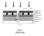
- FIG. 1The structure of a conventional prior art photovoltaic cell panel is shown in FIG. 1 . Because of the large range in the thickness of the different layers, they are depicted schematically. Moreover, FIG. 1 is highly schematized so that it will represent the features of both “thick-film” photovoltaic cells and “thin-film” photovoltaic cells.
- photovoltaic cells that use an indirect band gap material to absorb lightare typically configured as “thick-film” photovoltaic cells because a thick film of the absorber layer is required to absorb a sufficient amount of light.
- Photovoltaic cells that use direct band gap materials to absorb lightare typically configured as “thin-film” photovoltaic cells because only a thin layer of the direct band-gap material is need to absorb a sufficient amount of light.
- Layer (element) 102is the substrate. Glass or metal is a common substrate. In thin-film photovoltaic cells, substrate 102 can be-a polymer-based backing, metal, or glass. In some instances, there is an encapsulation layer, not shown, coating substrate 102 .
- Layer 104is the back electrical contact for the photovoltaic cell. It makes ohmic contact with the absorber layer of semiconductor junction 106 .
- Layer 106is the semiconductor absorber layer. In many but not all cases, it is a p-type semiconductor. Absorber layer 106 is thick enough to absorb light.
- Layer 108is the semiconductor junction partner-that completes the formation of a p-n junction, which is a common type of junction found in photovoltaic cells. In a photovoltaic cell based on a p-n junction, when absorber 106 is a p-type doped material, junction partner 108 is an n-type doped material. Conversely, when layer 106 is an n-type doped material, layer 108 is a p-type doped material. Generally, junction partner 108 is much thinner than absorber 106 . For example, in some instances junction partner 108 has a thickness of about 0.05 microns. Junction partner 108 is highly transparent to solar radiation. Junction partner 108 is also known as the window layer, since it lets the light pass down to absorber layer 106 .
- layers 106 and 108can be made from the same semiconductor material but have different carrier types (dopants) and/or carrier concentrations in order to give the two layers their distinct p-type and n-type properties.
- dopantscopper-indium-gallium-diselenide
- the use of CdS to form layer 108has resulted in high efficiency cells.
- Other materials that can be used for layer 108include, but are not limited to, SnO 2 , ZnO, ZrO 2 and doped ZnO.
- Layer 110is the top transparent electrode, which completes the functioning cell. Layer 110 is used to draw current away from the junction since junction partner 108 is generally too resistive to serve this function. As such, layer 110 should be highly conductive and transparent to light. Layer 110 can in fact be a comb-like structure of metal printed onto layer 108 rather than forming a discrete layer. Layer 110 is typically a transparent conductive oxide (TCO) such as zinc oxide (ZnO), indium-tin-oxide (ITO), or tin oxide (SnO 2 ). However, even when a TCO layer is present, a bus bar network 114 is typically needed to draw off current since the TCO has too much resistance to efficiently perform this function in larger photovoltaic cells.
- TCOtransparent conductive oxide
- ZnOzinc oxide
- ITOindium-tin-oxide
- SnO 2tin oxide
- Network 114shortens the distance charger carriers must move in the TCO layer in order to reach the metal contact, thereby reducing resistive losses.
- the metal bus barsalso termed grid lines, can be made of any reasonably conductive metal such as, for example, silver, steel or aluminum. There is design a tradeoff in network 114 between thicker grid lines that are more electrically conductive but block more light, and thin grid lines that are less electrically conductive but block less light.
- the metal barsare preferably configured in a comb-like arrangement to permit light rays through TCO layer 110 .
- Bus bar network layer 114 and TCO layer 110combined, act as a single metallurgical unit, functionally interfacing with a first ohmic contact to form a current collection circuit.
- Layer 112is an antireflection (AR) coating, which can allow a significant amount of extra light into the cell. Depending on the intended use of the cell, it might be deposited directly on the top conductor (as illustrated), or on a separate cover glass, or both. Ideally, the AR coating reduces the reflection of the cell to very near zero over the spectral region that photoelectric absorption occurs, and at the same time increases the reflection in the other spectral regions to reduce heating.
- ARantireflection
- Photovoltaic cellstypically produce only a small voltage.
- silicon based photovoltaic cellsproduce a voltage of about 0.6 volts (V).
- V0.6 volts
- photovoltaic cellsare interconnected in series or parallel in order to get a reasonable voltage.
- voltages of individual cellsadd together while current remains the same.
- photovoltaic cells arranged in seriesreduce the amount of current flow through such cells, compared to analogous photovoltaic cells arrange in parallel, thereby improving efficiency.
- the arrangement of photovoltaic cells in seriesis accomplished using interconnects 116 .
- an interconnect 116places the first electrode of one photovoltaic cell in electrical communication with the counterelectrode of an adjoining photovoltaic cell.
- conventional photovoltaic cellsare typically in the form of a plate structure. Although such cells are highly efficient when they are smaller, larger planar photovoltaic cells have reduced efficiency because it is harder to make the semiconductor films that form the junction in such photovoltaic cells uniform. Furthermore, the occurrence of pinholes and similar flaws increase in larger planar photovoltaic cells. These features can cause shunts across the junction.
- junction typeDetailed descriptions of various types of photovoltaic cells within the scope of the present invention, as defined by junction type, are in Section 5.4, below.
- photovoltaic cellsfunction by converting solar radiation into electrical energy.
- efficiency of a specific type of photovoltaic cellis proportional to the amount of photovoltaic radiation that is absorbed by the cell.
- Such absorptionis influenced by numerous conditions including but not limited to cloud cover, location, geographic latitude, and time of the day. For example, an extremely cloudy day reduces the amount of photovoltaic radiation available for absorption by a photovoltaic cell system.
- workershave developed photovoltaic cell architectures such as the bi-facial photovoltaic array that has both a front and a back panel.
- U.S. Pat. No. 5,990,413 to Ortabasi et al.describes such photovoltaic cell panels.
- the goal of the bi-facial designis to take advantage of both direct solar radiation and albedo.
- Albedois the fraction of incident electromagnetic radiation reflected by a surface. Albedo measures the reflectivity of a surface or body. It is the ratio of electromagnetic radiation reflected to the amount incident upon it. This ratio is a percentage that ranges anywhere from zero percent to one hundred percent. The amount of albedo a material exhibits is a function of its physical properties. Albedo is a product of the reflection of the incident solar radiation by the surroundings of the photovoltaic cells, such as sand, snow, water, rocks, grass, and buildings. Albedo is strongly dependent upon the nature of the environment. For example, albedo due to fresh snow can be higher than seventy percent while albedo due to large bodies of water is less than ten percent. In some instances, enhanced albedo improves the efficiency of existing photovoltaic cell assemblies.
- cleaning albedo surfacesis a necessary task in order to maintain the albedo properties of such surfaces
- cleaning of photovoltaic cell panels themselvesis necessary as well.
- cleaninghas the same drawbacks as the cleaning of albedo surfaces. Namely, such cleaning is time consuming, can degrade the material properties of the panels through adverse interaction (chemical, abrasive, or otherwise) with the cleaning agents, and is expensive.
- cleaningmay be necessary since any debris build up on photovoltaic cell panel surfaces adversely affects their efficiency.
- the present inventionprovides systems and methods for maintaining the efficiency of photovoltaic cells.
- the present inventionprovides systems and methods for maintaining self-cleaning albedo surfaces and self-cleaning photovoltaic cell panels.
- Self-cleaning albedo surfaces and photovoltaic cell panelsare produced by applying one or more layers of self-cleaning material onto the surface of photovoltaic cell panels as well as albedo surfaces. In this way, the drawbacks found in the prior art, namely laborious time consuming cleaning and repainting efforts, are minimized, thereby yielding a more efficient cost effective photovoltaic cell system.
- One aspect of the inventionprovides a photovoltaic cell system comprising a plurality of photovoltaic cell assemblies.
- Each assembly in the plurality of photovoltaic cell assembliescomprises a front side. Each of these front sides is configured to receive electromagnetic energy.
- Each of the photovoltaic assemblies in the plurality of photovoltaic assembliesis configured to convert electromagnetic energy into an electrical current.
- the photovoltaic cell systemfurther comprises an albedo surface configured to reflect electromagnetic energy on one or more photovoltaic cell assemblies in the plurality of photovoltaic cell assemblies.
- the albedo surfacecomprises a high albedo layer and a self-cleaning layer disposed on the high albedo layer.
- the self-cleaning layercomprises a photocatalytic material, Ti-hydroxyapetite, anatase TiO 2 , brookitein TiO 2 or rutile TiO 2 . In some embodiments, the self-cleaning layer comprises between 1 percent TiO 2 and 90 percent TiO 2 by weight. In some embodiments, the self-cleaning layer comprises ZnO, SnO 2 , SrTiO 3 , WO 3 , Bi 2 O 3 , Fe 2 O 3 , TEFLON®, polytetrafluoroethylene or polychlorotrifluoroethylene. In some embodiments, the self-cleaning layer is formed from perotitanium solution or perox-modified anatase sol.
- the self-cleaning layercomprises a plurality of nano-particles.
- Such nano-particlescan comprise, for example SiO 2 , TiO 2 , Al 2 O 3 , ZrO 2 or SnO 2 , silica, or any combination thereof.
- the self-cleaning layercomprises (100-X)CaF 2 -(X)TiO 2 , where X is the molar percentage of TiO 2 and X is between 1 percent and 50 percent.
- the self-cleaning layercomprises a composite of CaF 2 and TiO 2 .
- a photovoltaic cell systemcomprising a plurality of photovoltaic cell assemblies.
- Each assembly in the plurality of photovoltaic cell assembliescomprises a base, a solar cell panel attached to the base, and a self-cleaning albedo device attached to the base.
- the self-cleaning albedo devicecomprises a flexible substrate, a high albedo layer, and a self-cleaning layer.
- the high albedo layeris disposed on the flexible substrate and the self-cleaning layer is disposed on the high albedo layer.
- a photovoltaic cell system in accordance with this aspect of the inventioncomprises a retractable roller mounted on the base of an assembly in the plurality of photovoltaic assemblies for retracting the self-cleaning albedo device into a roll.
- the self-cleaning albedo devicehas an open configuration and a closed configuration. The self-cleaning albedo device is rolled up in the retractable roller when the self-cleaning albedo device is in the closed position. The self-cleaning albedo device is extended in a downward gradient away from the base when the self-cleaning albedo device is in the open position.
- the self-cleaning layercomprises a photocatalytic material, Ti-hydroxyapetite, anatase TiO 2 , rutile TiO 2 or brookitein TiO 2 . In some embodiments, the self-cleaning layer comprises between 1 percent TiO 2 and 90 percent TiO 2 by weight. In some embodiments, the self-cleaning layer comprises ZnO, SnO 2 , SrTiO 3 , WO 3 , Bi 2 O 3 , Fe 2 O 3 , TEFLON®, polytetrafluoroethylene or polychlorotrifluoroethylene. In some embodiments, the self-cleaning layer is formed from perotitanium solution or perox-modified anatase sol.
- the self-cleaning layercomprises a plurality of nano-particles.
- Such nano-particlescan comprise, for example SiO 2 , TiO 2 , Al 2 O 3 , ZrO 2 or SnO 2 , silica, or any combination thereof.
- the self-cleaning layercomprises (100-X)CaF 2 -(X)TiO 2 , where X is the molar percentage of TiO 2 and X is between 1 percent and 50 percent.
- the self-cleaning layercomprises a composite of CaF 2 and TiO 2 .
- Still another aspect of the present inventionprovides an albedo protective composite for use with photovoltaic cells.
- the albedo compositecomprises a high albedo layer and a self-cleaning layer.
- the high albedo layerhas an albedo value of twenty percent or greater, twenty-five percent or greater, thirty percent or greater, thirty-five percent or greater, forty percent or greater, forty-five percent or greater, fifty percent or greater, or fifty-five percent or greater.
- the high albedo layerhas an albedo of sixty percent or greater, sixty-five percent or greater, seventy percent or greater, seventy-five percent or greater, eighty percent or greater, eighty -five percent or greater, ninety percent or greater or ninety-five percent or greater.
- the self-cleaning layercan be made of any of the materials described in relation to self-cleaning layers of other aspects of the invention described above.
- FIG. 1depicts a photovoltaic cell in accordance with the prior art.
- FIG. 2Adepicts a perspective view of a photovoltaic cell assembly in accordance with one embodiment of the present invention.
- FIG. 2Bdepicts a cross-sectional view of a photovoltaic cell assembly with portable self-cleaning albedo surfaces in accordance with one embodiment of the present invention.
- FIG. 3illustrates a bifacial photovoltaic cell assembly in accordance with an embodiment of the present invention.
- FIG. 4depicts a process for maintaining albedo surfaces and solar cells in accordance with one aspect of the present invention.
- FIG. 5depicts various junction types in photovoltaic cell systems in accordance with embodiments of the present invention.
- FIG. 6Adepicts a self-cleaning mechanism in a photocatalytic protective layer in accordance with an embodiment of the present invention.
- FIG. 6Bdepicts a hydrophilic mechanism in a photocatalytic self-cleaning protective layer in accordance with an embodiment of the present invention.
- FIG. 7depicts a self-cleaning mechanism of a non-photocatalytic hydrophobic protective layer in accordance with an embodiment of the present invention.
- the present inventionprovides systems and materials to improve photovoltaic cell performance by implementing a self-cleaning function on photovoltaic cells and/or on albedo surfaces in the vicinity of photovoltaic cell assemblies.
- One aspect of the inventionprovides materials for protecting albedo surfaces that surround photovoltaic cell assemblies, thereby maximizing energy input into the photovoltaic cell assemblies.
- Another aspect of the inventionprovides materials for self-cleaning photovoltaic cell panels, thereby maintaining their efficiency.
- a third aspect of the present inventionprovides designs for portable albedo collecting devices that are associated with photovoltaic cell assemblies to optimize energy efficiency.
- an albedo collector systemin accordance with the present invention comprises photovoltaic cell panels 210 and panel support systems 216 .
- photovoltaic cell panels 210are bifacial.
- each photovoltaic panel 210has a back surface 214 in addition to a front surface 212 .
- the present inventionis not limited to bifacial photovoltaic cell panels.
- Photovoltaic cell panels 210are generally mounted on a surface 202 , such as the Earth. Surface 202 is typically not reflective enough to produce a high albedo effect.
- high albedo layer 206that is comprised of a high albedo layer 206 of material such as white paint, white sand, white gravel, white reflective plastic, or any combination thereof.
- high albedo layer 206has an albedo of seventy percent or more, eight percent or more, ninety percent or more, ninety-five percent or more, or ninety eight percent or more.
- high albedo layer 206is coated with a self-cleaning layer 208 thereby alleviating the need for cleaning high albedo layer 206 .
- self-cleaning layer 208is a single layer.
- self-cleaning layer 208is, in fact, a plurality of layers.
- each such layercan made of the same or a different compound.
- Compounds that can be used to make self-cleaning layer 208are described below and include photo and non-photocatalytic materials, both hydrophobic and non-hydrophobic.
- the thickness of self-cleaning layer 208is not greater than 0.2 ⁇ m. With such a thickness, coloring of self-cleaning layer 208 due to the interference of light can be avoided. Moreover, self-cleaning layer 208 is more transparent when the layer is made thinner. Thus, in some embodiments, self-cleaning layer 208 is not greater than 0.1 ⁇ m.
- an optional reflector wall 204is used. Like ground 202 , optional reflector wall 204 is coated with high albedo layer 206 ′ such as white paint
- this high albedo layer 206 ′is coated with a self-cleaning layer 208 ′ so that high albedo layer 206 ′ does not have to be cleaned on a regular basis.
- the materials that can be used to form self-cleaning layer 208 ′are the same as those that can be used to form self-cleaning layer 208 .
- any description of a possible composition of self-cleaning layer 208is also a description of a possible composition for layer 208 ′.
- self-cleaning layer 208 and/or 208 ′is one or more layers of a photocatalytic material, such as titanium dioxide or titanium-based nanoparticles, and/or a hydrophobic coating, such as a silicone and/or acrylic resin.
- a photocatalytic materialsuch as titanium dioxide or titanium-based nanoparticles
- a hydrophobic coatingsuch as a silicone and/or acrylic resin.
- FIG. 3demonstrates this architecture.
- FIG. 3illustrates a bi-facial photovoltaic cell 300 .
- Substrate 102 , back-electrode 104 , absorber 106 , window layer 108 , top-electrode 110 , and optional bus bar network 114are as described above in conjunction with Fig. 1 .
- the assemblyis encapsulated with a material 302 , such as EVA, and encased by panels 304 .
- Panels 304are typically made of glass or a plastic such as TEDLAR®.
- FIG. 3is drawn as a bifacial assembly, the invention is not so limited. Photovoltaic cells that include just one absorbing face benefit from the advantages of the present invention as well.
- photovoltaic cell panel 300is coated with a self-cleaning layer 306 .
- self-cleaning layer 306is one or more layers of a photocatalytic material, such as titanium dioxide or titanium-based nanoparticles, and/or a non-photocatalytic hydrophobic coating, such as a blend of a silicone and/or acrylic resin.
- the thickness of self-cleaning layer 306is not greater than 0.2 ⁇ m. With such a thickness, coloring of self-cleaning layer 306 due to the interference of light can be avoided.
- self-cleaning layer 306is more transparent when the layer is made thinner. Thus, in some embodiments, self-cleaning layer 306 is not greater than 0.1 ⁇ m.
- the junctions in solar cells in FIG. 3are illustrated as a planar, the invention is not so limited. Within panels 304 and encapsulation layer 302 , the solar cell junctions can adopt any know solar cell configuration, include planar (as shown), wire based, or rod based. As such, in some embodiments, panels 304 encase a series of parallel wires, where each wire comprises an elongated back electrode core 104 , absorber 106 , window layer 108 , and top electrode 110 layers all circumferentially disposed on the elongated back electrode core 104 .
- each elongated solar cell in the plurality of elongated solar cellscomprises (i) a conductive core configured as a first electrode, (ii) a semiconductor junction circumferentially disposed on the conductive core, and (iii) a transparent conductive oxide layer disposed on the semiconductor junction.
- Elongated solar cells in the plurality of elongated solar cellsare geometrically arranged in a parallel or a near parallel manner thereby forming a planar array having a first face and a second face.
- the plurality of elongated solar cellsis arranged such that one or more elongated solar cells in the plurality of elongated solar cells do not contact adjacent elongated solar cells.
- the solar cell assemblyfurther comprises a plurality of electrode strips. Each respective electrode strip in the plurality of electrode strips is lengthwise disposed on a first side of a corresponding elongated solar cell in the plurality of elongated solar cells. The first side of the solar cell is part of the first face of the planar array.
- the solar cell assemblyfurther comprises a transparent electrically insulating substrate (panel 304 ) that covers all or a portion of the first face of the planar array.
- a first and second elongated solar cell in the plurality of elongated solar cellsare electrically connected in series by an electrical contact that connects the first electrode of the first elongated solar cell to the corresponding electrode strip of the second elongated solar cell.
- the plurality of elongated solar cellsis configured to receive direct light from the first face and the second face of the planar array.
- the flowchart depicted in FIG. 4illustrates two general approaches that improve the efficiency of photovoltaic cell assemblies.
- the first approachas depicted by steps 420 through 428 , aims to improve the amount of light energy delivered to photovoltaic systems.
- the first approachoperates on self-cleaning layer 208 as depicted in FIG. 2A .
- This approachincludes the addition of one or more albedo layers to enhance the albedo effect of surfaces in the vicinity of solar cell panels ( 424 ); protecting such albedo layers ( 426 ), and addition of a self-cleaning function to such layers ( 428 ).
- Practice of these stepscauses additional solar energy to be absorbed by photovoltaic systems in the form of albedo energy.
- the second approachaims to maintain the general energy conversion efficiency of existing photovoltaic systems (solar cells).
- This second approachoperates directly on solar cell panels such as those disclosed in FIG. 2A .
- This second approachinvolves maintaining the energy conversion efficiency of solar cell panels ( 410 ) and the addition of a self-cleaning to such solar cell panels ( 412 ).
- Novel systems and methodsfor example, as summarized by steps 430 , 432 , and 434 of FIG. 4 , operate on either albedo surfaces, as illustrated in FIG. 2 , and solar cells, as illustrated in FIG. 3 , to help improve efficiency.
- Aspects of steps 430 , 432 , and 434include adding a photocatalytic coating 610 to solar cells or albedo surfaces and/or a hydrophobic coating (e.g., micro- or nano-structured) to the same.
- Both photocatalytic and non-photocatalytic materialscan be used to realize self-cleaning albedo surfaces. Such materials can be either hydrophobic or hydrophilic.
- Some specific embodiments of the present inventionprovide a self-cleaning layer 208 comprising a photocatalytic material. As illustrated in FIG. 2 , self-cleaning layer 208 is applied over high albedo layer 206 .
- Some embodiments of the present inventionprovide a self-cleaning layer 208 that comprises a non-photocatalytic hydrophobic material.
- the photocatalytic or non-photocatalytic materialis transparent, it can be used in layer 306 ( FIG. 3 ) of solar cell assemblies.
- Photocatalytic materialis activated by solar radiation in a process termed photocatalysis. Such activation causes the surface to be hydrophilic.
- Titanium dioxide or titaniae.g., TiO 2
- TiO 2is a known photocatalysts. The preparation of TiO 2 is described, for example, in U.S. Pat. No. 6,699,317, which is hereby incorporated herein by reference in its entirety.
- TiO 2exists in at least three natural mineral forms: anatase, rutile or brookitein TiO 2 . Among the three natural mineral forms, anatase is the most photoactive. Because of its unique properties, anatase is a highly favored photocatalytic material.
- TiO 2can be used to form layer 306 ( FIG. 3 ) and/or self-cleaning layer 208 ( FIG. 2A and FIG. 2B ). In some embodiments of the present invention, TiO 2 , in the form of anatase, is present in layers 208 and 306 .
- Photocatalytic coatingscomprise materials that are light radiation sensitive.
- One such photocatalytic coatingis TiO 2 .
- the mechanism for a light-activated self-cleaning layer 208 and/or 306 made of a material such as TiO 2is illustrated in FIG. 6A .
- the mechanism illustrated in FIG. 6Adepicts TiO 2 will be appreciated, although it is not so limited. In fact, the mechanism explains a broad range of photocatalytic materials of which TiO 2 is just one example.
- the photocatalytic material, TiO 2 for exampleis chemically activated by solar light or ultraviolet (UV) radiation. Electrons in TiO 2 are excited by UV radiation.
- the resulting roaming electrons (e ⁇ )leave behind holes (h + ).
- Water, dirt, and other forms of debrisdeposit on the coated surface and either react with the electrons or donate their own electrons to fill the holes.
- This exchange in electronsgenerates highly reactive materials such as H 2 O 2 , OH ⁇ , and free oxygen radicals.
- the impurity or contaminant in the deposited layeris gradually decomposed.
- Photocatalytic material 610such as TiO 2
- resin 620for example, to form self-cleaning layer 208 .
- self-cleaning layer 208When exposed to UV radiation, water molecules on the surface of self-cleaning layer 208 are chemisorbed by both photocatalyst 610 and resin 620 . As a result, the surface of self-cleaning layer 208 becomes increasingly hydrophilic. Water spreads over the surface in a thin film instead of forming droplets. The decomposed organic and inorganic debris then gets washed away when exposed to water (e.g., rain). Thus, photocatalytic materials render a surface self-cleaning by chemically breaking up dirt and causing it to wash away Some photocatalytic materials in accordance with the present invention are hydrophobic rather than hydrophilic. In some embodiments, the self-cleaning surface has combined hydrophilic and hydrophobic properties.
- U.S. Pat. No. 6,337,129 to Watanabe et al.which is hereby incorporated herein by reference in its entirety, describes bi-characteristic coating compositions that can be used in layers 306 in accordance with the present invention.
- TiO 2has a band gap of 3.2 eV, which allows the oxide to absorb light with wavelengths shorter than 385 nm. Solar radiation, however, contains only a very narrow wavelength range of such high energy rays.
- Systems and methodshave been developed to render TiO 2 more photoactive to radiation with longer wavelengths and hence less energy.
- the photocatalytic property of TiO 2can be altered by adding dopant, such as metallic ions like Ce. Ce retards the phase transition from reactive anatase to inert rutile so that the photocatalytic coating layer remains more sensitive to UV radiation for a longer time.
- the Ce-doped TiO 2 nano particleshave better band gap and modified solar absorption.
- layers 306 and/or self-cleaning 208comprise doped TiO 2 .
- layers 306 and/or self-cleaning layer 208comprise anatase, TiO 2 , rutile TiO 2 , brookitein TiO 2 , anatase sol, peroxo-modified anatase (Kon Corporation, Kishima-gun, Saga-prefecture Japan), and peroxotitanium acid (Kon Corporation).
- layers 306 and/or self-cleaning layer 208comprise ZnO, SnO 2 , SrTiO 3 , WO 3 , Bi 2 O 3 , Fe 2 O 3 , or any combination thereof.
- inorganic oxidesare combined with photocatalysts 610 to form self-cleaning layer 208 .
- the inorganic oxidesinclude, but are not limited to silica, alumina, water glass, silicate, aluminosilicate, zirconia, ceria, tin oxide, calcia, magnesia, amorphous titania and other metal oxides.
- such materialsare hydrophilified by photocatalytic action of the photocatalytic oxide.
- the present inventionprovides no limits on the amount of photocatalytic materials present in layers 208 and 306 .
- the amount of the photocatalytic material in layer 208 and/or 306can be between 1 percent and 90 percent by weight, between 20 percent and 70 percent by weight, or between 20 percent and 50 percent by weight.
- the balance of such layers 208 and 306comprises optional resin 620 ( FIG. 6B ), optional inorganic oxides 630 ( FIG. 6B ) and any other filler materials, at all possible combinations of ratios.
- layer 208 and/or 306be hydrophilic.
- Ti-hydroxyapatiteobtained, for example, by using titanium to replace calcium in Ca-hydroxyapatite (CaHAP), shares the same photocatalytic properties as TiO 2 .
- TiHAPis different from a composite of TiO 2 and hydroxyapatite. It has a low refractive index and high UV adsorption power, but it does not provide the photo-induced hydrophilicity ( Nonami et al., Mater. Res. Bull., 33, pp 125, 1998, which is hereby incorporated herein by reference in its entirety). Nevertheless, although it is not hydrophilic, Ti-hydroxyapatite (TiHAP) is a suitable material for use in self-cleaning layer 208 and/or 306 in accordance with embodiments of the present invention.
- self-cleaning layer 208 and/or 306has both hydrophilic and hydrophobic properties.
- self-cleaning layer 208comprises a photocatalytic oxide 610 and resin 620 .
- Resincomprises a silicone resin or silica, and a water-repellent fluororesin.
- the silicone or silica and the water-repellent fluororesinare present in a microscopically dispersed and exposed state on the surface of self-cleaning layer 208 and/or 306 .
- self-cleaning layer 208comprises a photocatalytic oxide (e.g., 610 of FIG. 6B ), supporting resin (e.g., 620 of FIG. 6B ), and optional inorganic oxide (e.g., 630 of FIG. 6B ) have been described.
- exemplary photocatalytic oxides, supporting resins, and optional inorganic oxides of the present inventioninclude, but are not limited to, any chemically stable combination of compounds listed in Table 1 below.
- Photocatalytic materialse.g., 610 of FIG. 6B
- Photocatalytic oxidesanatase TiO 2 rutile TiO 2 brookitein TiO 2 ZnO SnO 2 SrTiO 3 WO 3 Bi 2 O 3 Fe 2 O 3 peroxotitanium acid peroxo-modified anatase sol
- Resinse.g., 620 of FIG.
- silicone resin or silica methyltrimethoxysilanefor imparting methyltriethoxysilane hydrophilic or methyltrichlorosilane hydrophobic properties) methyltribromosilane methyltriisopropoxysilane methyl-tri-t-butoxysilane ethyltrimethoxysilane ethyltriethoxysilane ethyltrichlorosilane ethyltribromosilane ethyltriisopropoxysilane ethyl-tri-t-butoxysilane n-propyltrimethoxysilane n-propyltriethoxysilane n-propyltrichlorosilane n-propyltribromosilane n-propyltriisopropoxysilane n-propyl-tri-t-butoxysilane n-hexyltrimethoxysilane n-hexyltrimethoxys
- a transparent coatingis used for layer 306 and/or self-cleaning layer 208 .
- the photocatalytic coating materialsare available as water-based solutions (e.g., Titernal W, Fushimi Co. Mizoguchi, Sanda City, Hyogo Japan) or ethanol-based solutions (e.g., Titernal E, Fushimi Co.). In some embodiments, such solutions are sprayed onto high albedo layer 206 and panel 304 in order to form self-cleaning layers 208 and/or 306 .
- self-cleaning layer 208 and/or layer 306is formed using a reverse micelle dip coating method in which a transparent nano-crystalline TiO 2 thin film is deposited.
- a surfactante.g., Triton X-100
- a co-surfactante.g., hexanol
- a continuous phasee.g., cyclohexane
- titanium isopropoxideare mixed together.
- the solutionis applied to the proper surface (e.g., surface 304 ), for example, by dip coating. After drying and calcination in air, a multifunctional thin film of nano-crystalline TiO 2 is formed.
- application of the micelle solution in order to form self-cleaning layer 208 and/or layer 306comprises removing excess solution, padding the surface, and heating the surface (e.g., to over 90° C). See, for example, Daoud et al., 2004, J. Am. Ceram. Soc. 87, p. 953-555, which is hereby incorporated herein by reference in its entirety.
- self-cleaning layer 208 and/or layer 306is formed from a peroxotitanium acid solution.
- the solutioncomprises peroxotitanium acid anywhere from 0.3% by weight up to the maximum allowed by the solubility of peroxotitanium acid in solution.
- examples of such a solutioninclude, but are not limited to, PTA-85 and PTA-170 (Green Millennium, Los Angeles, Calif.), which comprises peroxotitanium acid at 0.85% and 1.7% by weight, respectively.
- self-cleaning layer 208 and/or layer 306is a self-cleaning photocatalytic coating material formed from peroxo-modified anatase sol.
- the solutioncomprises from peroxo-modified anatase sol anywhere from 0.3% by weight up to the maximum allowed by the solubility of peroxo-modified anatase sol in solution. Examples of such a solution include, but are not limited to, peroxo-modified anatase sol (Green Millennium, Los Angeles, Calif.) at 0.85% and 2.2% by weight, respectively.
- self-cleaning layer 208 and/or layer 306is a self-cleaning photocatalytic coating material formed from a mixture of peroxo-modified anatase sol and peroxotitanium acid.
- the solutioncomprises peroxo-modified anatase sol and peroxotitanium acid anywhere from 0.3% by weight up to the maximum allowed by the solubility of these compounds in solution.
- the mixture of peroxo-modified anatase sol and peroxotitanium acidcomprises two components at any ratio.
- TPX-85 and TPX-220Green Millennium, Los Angeles, Calif.
- peroxo-modified anatase soland peroxotitanium acid at 0.85% and 2.2% by weight, respectively.
- a hybrid systemis used to apply self-cleaning layer 208 and/or layer 306 when such a layer is made from anatase TiO 2 .
- the hybrid systemutilizes an inert sol-gel coating and a layer of anatase TiO 2 on top.
- a sol-gel layer 620acts to adhere nano-sized TiO 2 particles 610 .
- Layer 620also acts as a barrier to protect high albedo layer 206 from photocatalytic reactions.
- a suitable transparent coating of TiO 2is applied by methods such as painting (e.g., spraying, roller painting, etc., followed by optional heat treatment) to form self-cleaning layer 208 and/or 306 .
- layer 306 and/or self-cleaning layer 208comprises TiHAP, and is applied as a spray paint.
- layer 306 and 304is purchased as an assembled composite comprising a glass pane (layer 304 ) that has already been coated with a photocatalytic layer 306 . Examples of such assembled composites include, but are not limited to, ACTIVTM glass from Pilkington Holdings Inc. (Toledo, Ohio).
- a coating of an amorphous form of titaniais deposited and then calcined to thereby transform by phase transition the amorphous titania into crystalline titania (e.g., anatase, rutile or, brookitein).
- crystalline titaniae.g., anatase, rutile or, brookitein.
- high albedo layer 206is highly heat resistant (e.g., white gravel, white sand, white cement, etc.).
- Formation of amorphous titaniacan be carried out by one of the following methods.
- titanium alkoxideUpon drying, hydrolysis of titanium alkoxide will be completed to result in the formation of titanium hydroxide which then undergoes dehydration polymerization whereby a layer of amorphous titania is formed on the surface of the substrate (e.g., on layer 206 ).
- other organic compounds of titaniumsuch as chelate of titanium or acetate of titanium may be employed.
- Amorphous Titaniafrom Inorganic Titanium Compound.
- An acidic aqueous solution of an inorganic compound of titaniumsuch as TiCl 4 or Ti(SO 4 ) 2 is applied to the surface of a substrate by spray coating, flow coating, spin coating, dip coating, or roll coating.
- the substrateis then dried at a temperature of 100-200° C. to subject the inorganic compound of titanium to hydrolysis and dehydration polymerization to form a layer of amorphous titania on the surface of the substrate.
- amorphous titaniamay be formed on the surface of the substrate by chemical vapor deposition of TiCl 4 .
- Amorphous titaniacan be deposited on the surface of the substrate (e.g., onto layer 206 ) by bombarding a target of metallic titanium with an electron beam in an oxidizing atmosphere.
- Calcination of amorphous titaniacan be carried out at a temperature at least higher than the crystallization temperature of anatase. Upon calcination at a temperature of 400-500° C. or more, amorphous titania can be transformed into the anatase form of titania. Upon calcination at a temperature of 600-700° C. or more, amorphous titania can be transformed into the rutile form of titania.
- layer 208 and/or 306comprises a mixture of titania and silica.
- the ratio of silica to the sum of titania and silicacan be 5-90%, preferably 10-70%, more preferably 10-50%.
- the formation of a layer 208 and/or 306 comprised of silica-blended titaniacan be carried out by any of the following methods.
- a suspension containing particles of the anatase form or rutile form of titania and particles of silicais applied to panel 304 and/or high albedo layer 206 , followed by sintering at a temperature less than the softening point of panel 304 and or high albedo layer 206 .
- a mixture of a precursor of amorphous silicae.g., tetraalkoxysilane such as tetraethoxysilane, tetraisopropoxysilane, tetra-n-propoxysilane, tetrabuthoxysilane, and tetramethoxysilane; silanol formed by hydrolysis of tetraalkoxysilane; or polysiloxane having a mean molecular weight of less than 3000) and a crystalline titania sol is applied to panel 304 and/or high albedo layer 206 and is subjected to hydrolysis where desired to form silanol, followed by heating at a temperature higher than about 100° C.
- amorphous silicae.g., tetraalkoxysilane such as tetraethoxysilane, tetraisopropoxysilane, tetra-n-propoxysilane, te
- silanolto subject the silanol to dehydration polymerization to thereby form a photocatalytic coating wherein titania particles are bound by amorphous silica.
- dehydration polymerization of silanolis carried out at a temperature higher than about 200° C., polymerization of silanol is accomplished to a high degree so that the alkali resistance of the photocatalytic coating is enhanced.
- a suspension comprised of particles of silica dispersed in a solution of a precursor of amorphous titaniae.g., an organic compound of titanium such as alkoxide, chelate or acetate of titanium; or an inorganic compound of titanium such as TiCl 4 and Ti(SO 4 ) 2
- a precursor of amorphous titaniae.g., an organic compound of titanium such as alkoxide, chelate or acetate of titanium; or an inorganic compound of titanium such as TiCl 4 and Ti(SO 4 ) 2
- the precursoris subjected to hydrolysis and dehydration polymerization at a temperature ranging from the ambient temperature to 200° C. to thereby form a thin film of amorphous titania such that particles of silica are dispersed.
- the thin filmis heated at a temperature higher than the crystallization temperature of titania but lower than the softening point of the substrate to thereby transform amorphous titania into crystalline titania by
- a precursor of amorphous titaniae.g., an organic compound of titanium such as an alkoxide, chelate or acetate of titanium; or an inorganic compound of titanium such as TiCl 4 or Ti(SO 4 ) 2
- a precursor of amorphous silicae.g., a tetraalkoxysilane such as tetraethoxysilane, tetraisopropoxysilane, tetra-n-propoxy-silane, tetrabuthoxysilane, or tetramethoxysilane; a hydrolyzate thereof, e.g., silanol; or a polysiloxane having a mean molecular weight of less than 3000) and the mixture is applied to panel 304 and/or high albedo layer 206 .
- a tetraalkoxysilanesuch as tetraethoxysilane, tetraisopropoxys
- these precursorsare subjected to hydrolysis and dehydration polymerization to form a thin film made of a mixture of amorphous titania and amorphous silica. Thereafter, the thin film is heated at a temperature higher than the crystallization temperature of titania but lower than the softening point of panel 304 and/or high albedo layer 206 to thereby transform amorphous titania into crystalline titania by phase transition.
- layer 208 and/or layer 306comprises a mixture of titania and tin oxide.
- the ratio of tin oxide to the sum of titania and tin oxidecan be 1-95% by weight, preferably 1-50% by weight.
- Formation of a layer 208 and/or layer 306 comprised of tin oxide-blended titaniacan be carried out by any of the following methods.
- a suspension containing particles of the anatase form or rutile form of titania and particles of tin oxideis applied to panel 304 and/or high albedo layer 206 , followed by sintering at a temperature less than the softening point of panel 304 and/or high albedo layer 206 .
- a suspension comprised of particles of tin oxide dispersed in a solution of a precursor of amorphous titaniae.g., an organic compound of titanium such as alkoxide, chelate or acetate of titanium; or an inorganic compound of titanium such as TiCl 4 or Ti(So 4 ) 2
- a precursor of amorphous titaniae.g., an organic compound of titanium such as alkoxide, chelate or acetate of titanium; or an inorganic compound of titanium such as TiCl 4 or Ti(So 4 ) 2
- the precursoris subjected to hydrolysis and dehydration polymerization at a temperature ranging from the ambient temperature to 200° C. to thereby form a thin film of amorphous titania such that particles of tin oxide are dispersed within the film.
- the thin filmis heated at a temperature higher than the crystallization temperature of titania but lower than the softening point of panel 304 and/or high albedo layer 206 to thereby transform amorphous titania into crystalline titania by phase transition.
- layer 208 and/or layer 306is a coating composition wherein particles of a photocatalyst are dispersed in a film forming element of uncured or partially cured silicone (organopolysiloxane) or a precursor thereof.
- the coating compositionis applied on panel 304 and/or high albedo layer 206 and the film-forming element is then subjected to curing.
- the organic groups bonded to the silicon atoms of the silicone moleculesare substituted with hydroxyl groups under the photocatalytic action of the photocatalyst.
- the photocatalyst-containing silicone paintcan be cured at ambient temperature or at a relatively low temperature, this method can be applied to a substrate formed of a non-heat-resistant material such as plastics.
- the coating composition containing the photocatalystcan be applied whenever desired by way of brush painting, spray coating, roll coating and the like on any existing substrate requiring superhydrophilification of the surface.
- layer 208 and/or 306is doped with a metal such as Ag, Cu and Zn.
- a metalsuch as Ag, Cu or Zn
- Doping of the layer with a metal such as Ag, Cu or Zncan be carried out by adding a soluble salt of such metal to a suspension containing particles of the photocatalyst, the resultant solution being used to form layer 208 and/or 306 .
- a soluble salt of such metalcan be applied thereon and can be subjected to irradiation of light to deposit the metal by photoreduction.
- layer 208 and/or 306 doped with a metal such as Ag, Cu or Znis capable of killing bacteria adhered to the surface. Moreover, it is believed that doped layers 208 and/or 306 inhibit growth of microorganisms such as mold, algae and moss. As a result, albedo surface 206 and/or panel 304 are clean for a longer period.
- layer 208 and/or 306can additionally be doped with a metal of the platinum group such as Pt, Pd, Rh, Ru or Ir. These metals can be similarly doped into the composition used to make layer 208 and/or 306 by photoreduction deposition or by addition of a soluble salt.
- a layer 208 and/or 306 doped with a metal of the platinum groupdevelops an enhanced photocatalytic redox activity so that decomposition of contaminants adhering on the surface is promoted.
- layer 208 and 206is a single combined layer comprising white paint that is doped with any of the photoactive materials described in this section. Properties of suitable white paints are described in the section below.
- combined layer 208 / 206is one or more layers of white paint that has been doped with TiO 2 , anatase TiO 2 , rutile TiO 2 , brookitein TiO 2 , ZnO, SnO 2 , SrTiO 3 , WO 3 , Bi 2 O 3 , or Fe 2 O 3 , or any combination of such dopants. In some embodiments, care is taken to ensure that such dopants are in the uppermost part of combined layer 208 / 206 by adding the dopant particles (e.g., TiO 2 ) while the paint is still wet.
- dopant particlese.g., TiO 2
- layer 208 and/or 306is administered using a hot aerosol layering operation.
- a hot aerosol layering operationSuch processes have been developed by companies such as Nextrom (Duluth, Georgia and Camarillo, Calif.).
- the hot aerosol processis based on the combustion of liquid raw materials in an atmospheric flame. As the precursor liquid is atomized, the droplets containing the raw materials and solvent evaporate, and finally condense again to become homogeneous, nano-sized particles, that are deposited on layer 206 and/or 304 .
- self-cleaning layers 208 and 306are self-cleaned through mechanisms other than a primary photocatalytic mechanism.
- self-cleaning layers 208 and/or 306have a self-cleaning property through some mechanism independent of a photocatalytic property. This does not necessarily mean that such layers do not include photocatalytic materials and that some self-cleaning functionality is present in such materials.
- some of the compositions of matter described in this sectionare photocatalytic. However, in each instance, the compositions in this section provide a self-cleaning functionality by way of a mechanism that is additional to or lieu of a photocatalytic mechanism.
- self-cleaning layer 208 and/or layer 306is a hydrophobic material.
- a drop of water touches a solid surfaceboth the solid surface and the drop are surrounded by air at the same time ( FIG. 7A ).
- the interactions at this “three-phase boundary”determine the shape of the drop and how well or poorly the liquid spreads over the solid surface, in other words, how well it wets the solid substrate.
- One way of measuring thisis the contact angle ⁇ ( FIG. 7A ).
- TeflonWhen a drop of water contacts a cleaned glass surface, the contact angle ⁇ is around 15 degrees whereas by comparison, the same drop of water is on a Teflon coated surface forms a contact angle of 109° .
- Teflonabsorbs light in the upper visible and UV ranges (Seres et al., 1994, Opt. Eng. 33, p. 3031-3033, which is hereby incorporated herein by reference in its entirety) and in the infrared region between 6 ⁇ m to 8 ⁇ m (Hollahan et al., 1974, Applied Opt. 13, p. 1844-1849, which is hereby incorporated herein by reference in its entirety).
- Such absorptioncompromises the efficiency of solar energy conversion. Therefore, the use of TEFLON® coating for use as self-cleaning layers 208 and/or 306 may be limited.
- TEFLON® materialis a water repellant coating constructed from a composite material of CaF 2 and TiO 2 , as described by Tsai et al., in U.S. Pat. No. 6,383,629, which is hereby incorporated herein by reference in its entirety. Though the composite material of CaF 2 and TiO 2 does not have a contact angle ⁇ that is significantly better than that of Teflon, it does not have the optical limitations of Teflon material.
- self-cleaning layer 208 and/or layer 306is made of polytetrafluoroethylene (PTFE) [—CF 2 —CF 2 —] n or polychlorotrifluoroethylene (PCTFE) [—CF 2 —CFCl—] n .
- PTFEpolytetrafluoroethylene
- PCTFEpolychlorotrifluoroethylene
- self-cleaning layer 208comprises a Teflon TEFLON® coating. See, for example, U.S. Pat. No. 4,869,922 to D'Agositno, U.S. Pat. No. 4,410,563 to Richter and Dibble, as well as Hollahan et al., Applied Opt. 13, p.
- self-cleaning layer 208comprises CaF 2 and TiO 2 .
- self-cleaning layer 208comprises a material having a chemical formula (100-X)CaF 2 —(X)TiO 2 , where X is the molar percentage of TiO 2 .
- Xis between 1 percent and 50 percent.
- Xis between 2 percent and 45 percent.
- Xis between 10 percent and 30 percent.
- the Lotus-Effectis used to provide desired self-cleaning properties like that found in plant leaves such as the Sacred Water Lilly ( Nelumbo nucifera ).
- the Lotus-Effectis based on the interaction between a solid surface (lotus leaf) and its environment (water droplets), and is therefore a surface phenomenon. Electron microscopy study of the lotus leaves revealed that they have “rough” surfaces of small humps and some fronds (e.g., 710 in FIG. 7C ). In addition, the surfaces of the lotus leaves are coated by hydrophobic wax-like material (e.g. 720 in FIG. 7C ).
- self-cleaning layer 208 and/or layer 306is a rough surface comprising hydrophobic nano- or micro-structured surfaces as illustrated in FIG. 7B .
- such structured surfacescause water to have a contact angle ⁇ that exceeds 160 degree.
- the size of the surface structurese.g., 710 in FIG. 7C ) ranges from several nanometers up to 50 microns.
- hydrophobic coatingse.g., 720 in FIG. 7C
- such “rough” surfacesare effectively hydrophobic.
- Spherical water dropletsroll off such surfaces (e.g., self-cleaning layer 208 or layer 306 in FIG. 7B and 7C ). Therefore, they remain dry even when it is raining.
- the materials used to make surface structures 710 and hydrophobic coatings 720are transparent. Such materials can therefore be used to form layer 306 on solar cells in addition to forming a self-cleaning layer 208 on high albedo layer 206 .
- Particles 710can be obtained in commercially available sizes and or by a precipitation processes such as, for example, by a pyrogenic process. Alternatively, particles 710 can be obtained be obtained from a gaseous starting material that is converted into a pulverulent substance.
- Particles 710can be any combination of the materials listed in Table 2 below.
- particles 710comprise oxides such as SiO 2 , TiO 2 , Al 2 O 3 , ZrO 2 or SnO 2 . These oxides are typically pyrogenically prepared oxides.
- particles 710are pyrogenic silica with an average primary particle size in the range between about 7 nm and 40 nm.
- particles 710comprise a silicate, a doped silicate, a mineral, a metal oxide, a silica, a polymer, and/or a coated metal powder.
- particles 710comprise fumed silica, precipitated silica, or a pulverulent polymer, e.g., a cryogenically milled or spray-dried polytetrafluoroethylene (PTFE).
- PTFEpolytetrafluoroethylene
- self-cleaning layer 208is LOTUSANTM paint (Sto, Germany).
- the paintcan be applied with brush, roller, or proper spray equipment.
- the LOTUSANTM paintcomprises 1-5% triethoxy (2, 4, 4-trimethylpentyl) silane, 15-40% Cristobalite (SiO 2 ), and 10-30% TiO 2 , by weight.
- the self-cleaning layeris a hydrophilic paint that comprises an acrylic resin, an acryl-silicone resin, an aqueous silicone, a block copolymer of silicone resin and acrylic resin, an acryl-styrene resin, an ethylene oxide of sorbitan fatty acid, an ester of sorbitan fatty acid, an acetate of urethane, a cross-linked urethane of polycarbonatediol and/or polyisocyanate, or a cross-linked polymer of alkylester polyacrylate.
- self-cleaning layer 208is a water-repellant paint containing polytetrafluoroethylene (PFTE).
- PFTEpolytetrafluoroethylene
- TiO 2 and other photocatalytic oxidesare found in Various hydrophobic coating materials listed herein, it is not because of their possible Photocatalystic properties. Rather, such oxides provide roughness and control the Formation of micro- or nano- structured surfaces.
- Exemplary materials for use in layers 208 and 306 in which photoactivity is not the primary basis for self-cleaningComponent Exemplary materials 1. Teflon Coating polytetrafluoroethylene (PTFE) polychlorotrifluoroethylene (PCTFE) 2. Composite inorganic coating CaF 2 and TiO 2 3. Coating based on Lotus Effect 3a. Structural forming material inorganic substances metal oxides mixed oxides silicates sulfates phosphates borates metal sulfides oxosulfides selenides sulfoselenides metal nitrides oxide nitrides Organic substances nanoscale organic polymeric particles nanoscale organic polymeric particles containing fluorine. 3b. Hydrophobic coating particles comprising PTFE or any other suitable hydrophobic materials
- high albedo layer 206 and self-cleaning layer 208form a single self-cleaning high albedo layer.
- the self-cleaning property in such a layercan be rendered by either a photocatalytic or hydrophobic mechanism.
- One embodiment in accordance with this aspect of the inventionis the application of white LOTUSANTM paint as a single combined layer 206 / 208 .
- device 220is attached to the base of photovoltaic cell supporting system 216 .
- device 220comprises a substrate 222 with a high albedo layer 206 disposed thereon.
- substrate 222is made of a highly flexible material that can be rolled or folded up.
- a high albedo layer 206for example, a layer of white paint or any of the materials described for layer 206 in preceding sections, is disposed on substrate 222 .
- flexible substrate 222is itself a high albedo material.
- High albedo layer 206is not necessary embodiments of device 220 where the substrate 222 has high albedo (e.g. albedo greater than ninety percent).
- self-cleaning layer 208is disposed on high albedo layer 206 (or directly onto flexible substrate 222 in instances where flexible substrate 222 possesses albedo properties and thus high albedo layer 206 is not present).
- device 220comprises a single layer of MYLAR® or any of a number of other low-cost plastics that can be manufactured with high albedo.
- flexible substrate 222is optional and often is not included.
- self-cleaning layer 208is not present as well.
- each solar cell assemblyincludes a respective device 220 as illustrated in FIG. 2B .
- device 220is rolled down the gradient. Thus, any water that lands on device 220 rolls down the gradient rather than collecting on the surface and forming water spots.
- device 220is a folded assembly instead of the roll-up type. Regardless of whether assembly 220 is of the roll-up type or the fold-up type, the assembly 220 will preferably attach to hooks on the bottom of each photovoltaic cell supporting system 216 in order to allow the device 220 to be removed to make room for maintenance.
- device 220is a plastic sheet that can be easily rolled or folded away, stored and assembled with any existing photovoltaic cell system. See Section 5.5 for more description of photovoltaic cell systems that can be used in the present invention.
- device 220is a self-cleaning albedo plastic sheet that can be rolled or folded out and attached to the base 216 of the photovoltaic cell support 216 by a hinge mechanism.
- substrate 222is a board that can be easily stored and assembled in any existing photovoltaic cell systems.
- High albedo layer 206for example a layer of white paint, is disposed upon substrate 222 .
- a self-cleaning layer 208is then disposed upon high albedo layer 206 .
- Some embodiments of the present inventionprovide a photovoltaic cell system comprising a plurality of photovoltaic cell assemblies.
- Each assembly in the plurality of photovoltaic cell assembliescomprises a base, a solar cell panel attached to the base, and a self-cleaning albedo device (e.g., device 220 of FIG. 2B ), attached to the base.
- the self-cleaning albedo devicecomprises a flexible substrate (e.g., 222 of FIG. 2B ), a high albedo layer (e.g., layer 206 of FIG. 2B ), and a self-cleaning layer (e.g., layer 208 of FIG. 2B ).
- the photovoltaic systemfurther comprises a retractable roller mounted on the base for retracting the self-cleaning albedo device into a roll.
- the self-cleaning albedo devicehas an open configuration and a closed configuration. The self-cleaning albedo device is rolled up in the retractable roller when the self-cleaning albedo device is in the closed position. Further, the self-cleaning albedo device is extended in a downward gradient away from the base when the self-cleaning albedo device is in the open position.
- semiconductor junction 510is a heterojunction between an absorber layer 502 , disposed on conductive core 510 , and a junction partner layer 510 , disposed on absorber layer 502 .
- Layers 502 and 504are composed of different semiconductors with different band gaps and electron affinities such that junction partner layer 510 has a larger band gap than absorber layer 502 .
- absorber layer 502is p-doped and junction partner layer 510 is n-doped.
- TCO layer 512is n + -doped.
- absorber layer 502is n-doped and junction partner layer 510 is p-doped.
- TCO layer 512is p + -doped.
- the semiconductors listed in Pandey, 1996, Handbook of semiconductor Electrodeposition , Marcel Dekker Inc., Appendix 5, which is hereby incorporated herein by reference in its entirety,are used to form semiconductor junction 510 .
- absorber layer 502is a group I-III-VI 2 compound such as copper indium di-selenide (CuInSe 2 ; also known as CIS).
- absorber layer 502is a group I-III-VI 2 ternary compound selected from the group consisting of CdGeAs 2 , ZnSnAs 2 , CuInTe 2 , AgInTe 2 , CuInSe 2 , CuGaTe 2 , ZnGeAs 2 , CdSnP 2 , AgInSe 2 , AgGaTe 2 , CuInS 2 , CdSiAs 2 , ZnSnP 2 , CdGeP 2 , ZnSnAs 2 , CuGaSe 2 , AgGaSe 2 , AgInS 2 , ZnGeP 2 , ZnSiAs 2 , ZnSiP 2 , CdGeP 2 , ZnSnAs 2 , CuG
- junction partner layer 510is CdS, ZnS, ZnSe, or CdZnS.
- absorber layer 502is p-type CIS and junction partner layer 510 is n-type CdS, ZnS, ZnSe, or CdZnS.
- Such semiconductor junctions 510are described in Chapter 6 of Bube, 1998, Photovoltaic Materials , Imperial College Press, London, which is hereby incorporated herein by reference in its entirety.
- absorber layer 502is copper-indium-gallium-diselenide (CIGS). In some embodiments, absorber layer 502 is copper-indium-gallium-diselenide (CIGS) and junction partner layer 510 is CdS, ZnS, ZnSe, or CdZnS. In some embodiments, absorber layer 502 is p-type CIGS and junction partner layer 510 is n-type CdS, ZnS, ZnSe, or CdZnS.
- CIGScopper-indium-gallium-diselenide
- junction partner layer 510is CdS, ZnS, ZnSe, or CdZnS.
- semiconductor junction 510comprises amorphous silicon. In some embodiments, this is an n/n type heterojunction.
- layer 514comprises SnO 2 (Sb)
- layer 512comprises undoped amorphous silicon
- layer 510comprises n+ doped amorphous silicon.
- semiconductor junction 510is a p-i-n type junction.
- layer 514is p + doped amorphous silicon
- layer 512is undoped amorphous silicon
- layer 510is n + amorphous silicon.
- Such semiconductor junctions 510are described in Chapter 3 of Bube, Photovoltaic Materials, 1998, Imperial College Press, London, which is hereby incorporated herein by reference in its entirety.
- semiconductor junction 510is based upon thin-film polycrystalline.
- layer 510is a p-doped polycrystalline silicon
- layer 512is depleted polycrystalline silicon
- layer 514is n-doped polycrystalline silicon.
- semiconductor junctionsare described in Green, 1995, Silicon Solar Cells: Advanced Principles & Practice , Centre for Photovoltaic Devices and Systems, University of New South Wales, Sydney; and Bube, 1998, Photovoltaic Materials , pp. 57-66, Imperial College Press, London, which is hereby incorporated herein by reference in its entirety.
- semiconductor junctions 510based upon p-type microcrystalline Si:H and microcrystalline Si:C:H in an amorphous Si:H photovoltaic cell are used. Such semiconductor junctions are described in Bube, 1998, Photovoltaic Materials , pp. 66-67, Imperial College Press, London, and the references cited therein, which is hereby incorporated herein by reference in its entirety.
- semiconductor junctions 510are based upon gallium arsenide (GaAs) or other III-V materials such as InP, AlSb, and CdTe.
- GaAsis a direct-band gap material having a band gap of 1.43 eV and can absorb 97% of AM 1 radiation in a thickness of about two microns.
- Suitable type III-V junctions that can serve as semiconductor junctions 510 of the present inventionare described in Chapter 4 of Bube, 1998, Photovoltaic Materials , Imperial College Press, London, which is hereby incorporated herein by reference in its entirety.
- semiconductor junction 510is a hybrid multijunction photovoltaic cells such as a GaAs/Si mechanically stacked multijunction as described by Gee and Virshup, 1988, 20 th IEEE Photovoltaic Specialist Conference , IEEE Publishing, New York, p. 754, which is hereby incorporated herein by reference in its entirety, a GaAs/CuInSe 2 MSMJ four-terminal device, consisting of a GaAs thin film top cell and a ZnCdS/CuInSe 2 thin bottom cell described by Stanbery et al., 19 th IEEE Photovoltaic Specialist Conference , IEEE Publishing, New York, p.
- a hybrid multijunction photovoltaic cellssuch as a GaAs/Si mechanically stacked multijunction as described by Gee and Virshup, 1988, 20 th IEEE Photovoltaic Specialist Conference , IEEE Publishing, New York, p. 754, which is hereby incorporated herein by reference in its entirety, a GaAs/CuInSe 2
- semiconductor junctions 510are based upon II-VI compounds that can be prepared in either the n-type or the p-type form. Accordingly, in some embodiments, referring to FIG. 5C , semiconductor junction 510 is a p-n heterojunction in which layers 520 and 540 are any combination set forth in the following table or alloys thereof.
- semiconductor junctions 510that are made from thin semiconductor films are preferred, the invention is not so limited. In some embodiments semiconductor junctions 510 is based upon crystalline silicon. For example, referring to FIG. 5D , in some embodiments, semiconductor junction 510 comprises a layer of p-type crystalline silicon 540 and a layer of n-type crystalline silicon 550 . Methods for manufacturing crystalline silicon semiconductor junctions 510 are described in Chapter 2 of Bube, Photovoltaic Materials, 1998, Imperial College Press, London, which is which is hereby incorporated herein by reference in its entirety.
- the self-cleaning surfaces of the present inventioncan be used with a wide variety of photovoltaic types including, but not limited to, wire-shaped, tube-shaped and flat panel-shaped.
- the self-cleaning surfaces of the present inventioncan be used with mono-facial, bi-facial, and multi-facial photovoltaic cells.
- the self-cleaning surfaces of the present inventioncan be used with moveable as well as stationary photovoltaic cells.
- the self-cleaning surfaces of the present inventioncan be used with photovoltaic cells having any of the junction types described in Section 5.4.
- the photovoltaic cells of the present inventioncan be used with photovoltaic cell concentrators.
- photovoltaic cells 210there is no limit to the types and architectures of photovoltaic cells 210 ( FIG. 2 ) that can benefit from the self-cleaning layers 208 and 306 of the present invention.
- Representative photovoltaic cells 210include, but are not limited to any of the photovoltaic cells described in U.S. Pat. Nos.
- Still another type of photovoltaic cell that can benefit from the self-cleaning layers of the present inventionare the type of photovoltaic cells found in U.S. Pat. No. 6,762,359 B2 to Asia et al., which is hereby incorporated herein by reference in its entirety, in which a photovoltaic cell including a p-type layer and an n-type layer is disclosed.
- Still another type of photovoltaic cell that can benefit from the self-cleaning layers of the present inventionis the type of photovoltaic cells found in U.S. Pat. No.
- Still another type of photovoltaic cell that can benefit from the self-cleaning layers of the present inventionare the type of photovoltaic cells found in Japanese Patent Application Kokai Publication Number S59-125670, Toppan Printing Company, published Jul. 20, 1984 (hereinafter “S59-125670”), which is hereby incorporated herein by reference in its entirety, in which a rod-shaped photovoltaic cell is disclosed.
- Photovoltaic cellthat can benefit from the self-cleaning layers of the present invention is the type of photovoltaic cells found in German Unexamined Patent Application DE 43 39 547 A1 to Twin Solar-Technik Anlagens-GmbH, published May 24, 1995, (hereinafter “Twin Solar”), which is hereby incorporated herein by reference in its entirety, in which a plurality of rod-shaped photovoltaic cells arranged in a parallel manner inside a transparent sheet, which forms the body of the photovoltaic cell.
- One aspect of the inventionprovides a photovoltaic cell system comprising a plurality of photovoltaic cell assemblies.
- Each assembly in the plurality of photovoltaic cell assembliescomprises a front side and a back side. Each of these front sides and back sides is configured to receive electromagnetic energy.
- Each of the photovoltaic assemblies in the plurality of photovoltaic assembliesis configured to convert electromagnetic energy into an electrical current.
- Each respective photovoltaic cell assembly in the plurality of photovoltaic cell assembliesfurther comprises a first self-cleaning layer disposed on the corresponding front side of the respective photovoltaic cell assembly.
- each respective photovoltaic cell assembly in the plurality of photovoltaic cell assembliesfurther comprises a second self-cleaning layer disposed on the corresponding back side of the respective photovoltaic cell assembly.
- the first self-cleaning layer and/or the second self-cleaning layeris one or more layers of photocatalytic coating, nano-particles and/or titanium oxide.
- the first self-cleaning layer and/or the second self-cleaning layeris a hydrophobic layer.
Landscapes
- Photovoltaic Devices (AREA)
- Paints Or Removers (AREA)
Abstract
Description
| TABLE 1 |
| Exemplary materials for assembling |
| Component | Exemplary materials |
| 1. Photocatalytic materials | |
| (e.g., 610 of FIG. 6B) | |
| photocatalytic oxides | anatase TiO2 |
| rutile TiO2 | |
| brookitein TiO2 | |
| ZnO | |
| SnO2 | |
| SrTiO3 | |
| WO3 | |
| Bi2O3 | |
| Fe2O3 | |
| peroxotitanium acid | |
| peroxo-modified anatase sol | |
| Apatite derivatives | Ti-HAP |
| 2. Resins | |
| (e.g., 620 of FIG. 6B) | |
| silicone resin or silica | methyltrimethoxysilane |
| (for imparting | methyltriethoxysilane |
| hydrophilic or | methyltrichlorosilane |
| hydrophobic properties) | methyltribromosilane |
| methyltriisopropoxysilane | |
| methyl-tri-t-butoxysilane | |
| ethyltrimethoxysilane | |
| ethyltriethoxysilane | |
| ethyltrichlorosilane | |
| ethyltribromosilane | |
| ethyltriisopropoxysilane | |
| ethyl-tri-t-butoxysilane | |
| n-propyltrimethoxysilane | |
| n-propyltriethoxysilane | |
| n-propyltrichlorosilane | |
| n-propyltribromosilane | |
| n-propyltriisopropoxysilane | |
| n-propyl-tri-t-butoxysilane | |
| n-hexyltrimethoxysilane | |
| n-hexyltriethoxysilane | |
| n-hexytrichlorosilane | |
| n-hexyltribromosilane | |
| n-hexyltriisopropoxysilane | |
| n-hexyl-tri-t-butoxysilane | |
| n-decyltrimethoxysilane | |
| n-decyltriethoxysilane | |
| n-decyltrichlorosilane | |
| n-decyltribromosilane | |
| n-decyltriisopropoxysilane | |
| n-decyl-tri-t-butoxysilane | |
| n-octatrimethoxysilane | |
| n-octatriethoxysilane | |
| n-octatrichlorosilane | |
| n-octatribromosilane | |
| n-octatriisopropoxysilane | |
| n-octa-tri-t-butoxysilane | |
| phenyltrimethoxysilane | |
| phenyltriethoxysilane | |
| phenyltrichlorosilane | |
| phenyltribromosilane | |
| phenyltriisopropoxysilane | |
| phenyl-t-butoxysilane | |
| dimethyldichlorosilane | |
| dimethyldibromosilane | |
| dimethyldimethoxysilane | |
| dimethyldiethoxysilane | |
| diphenyldichlorosilane | |
| diphenyldibromosilane | |
| diphenyldimethoxysilane | |
| diphenyldiethoxysilane | |
| phenylmethyldichlorosilane | |
| phenylmethyldibromosilane | |
| phenylmethyldimethoxysilane | |
| phenylmethyldiethoxysilane | |
| vinyltrichlorosilane | |
| vinyltribromosilane | |
| vinyltrimethoxysilane | |
| vinyltriethoxysilane | |
| vinyltriisopropoxysilane | |
| vinyl-tri-t-butoxysilane | |
| trifluoropropyltrichlorosilane | |
| trifluoropropyltribromosilane | |
| trifluoropropyltrimethoxysilane | |
| trifluoropropyltriethoxysilane | |
| trifluoropropyltriisopropoxysilane | |
| trifluoropropyl-tri-t-butoxysilane | |
| γ-glycidoxypropylmethyldimethoxysilane | |
| γ-glycidoxypropylmethyldiethoxysilane | |
| γ-glycidoxypropyltrimethoxysilane | |
| γ-glycidoxypropyltriethoxysilane | |
| γ-glycidoxypropyltriisopropoxysilane | |
| γ-glycidoxypropyl-tri-t-butoxysilane | |
| γ-methacryloxypropylmethyldimethoxysilane | |
| γ-methacryloxypropylmethyldiethoxysilane | |
| γ-methacryloxypropyltrimethoxysilane | |
| γ-methacryloxypropyltriethoxysilane | |
| γ-methacryloxypropyltriisopropoxysilane | |
| γ-methacryloxypropyl-tri-t-butoxysilane | |
| γ-aminopropylmethyldimethoxysilane | |
| γ-aminopropylmethyldiethoxysilane | |
| γ-aminopropyltrimethoxysilane | |
| γ-aminopropyltriethoxysilane | |
| γ-aminopropyltriisopropoxysilane | |
| γ-aminopropyl-tri-t-butoxysilane | |
| γ-mercaptopropylmethyldimethoxysilane | |
| γ-mercaptopropylmethyldiethoxysilane | |
| γ-mercaptopropyltrimethoxysilane | |
| γ-mercaptopropyltriethoxysilane | |
| γ-mercaptopropyltriisopropoxysilane | |
| γ-mercaptopropyl-tri-t-butoxysilane | |
| β-(3,4-poxycyclohexyl)ethyltrimethoxysilane | |
| β-(3,4-epoxycyclohexyl)ethyltriethoxysilane | |
| water-repellent fluoro- | polytetrafluoroethylene |
| resin | polyvinylidene fluoride |
| polyvinyl fluoride | |
| polychlorotrifluoroethylene | |
| tetrafluoroethylene/hexafluoropropylene | |
| copolymer | |
| ethylene/tetrafluoroethylene copolymer | |
| ethylene/chlorotrifluoroethylene copolymer | |
| tetrafluoroethylene/perfluoroalkyl vinyl ether | |
| copolymer | |
| perfluorocyclo polymer | |
| vinyl ether/fluoroolefin copolymer | |
| vinyl ester/fluoroolefin copolymer | |
| tetrafluoroethylene/vinyl ether copolymer | |
| chlorotrifluoroethylene/vinyl ether | |
| copolymer | |
| urethane-crosslinked tetrafluoroethylene | |
| epoxy-crosslinked tetrafluoroethylene | |
| acryl-crosslinked tetrafluoroethylene | |
| melamine-crosslinked tetrafluoroethylene | |
| 3. Inorganic oxide | silica |
| (e.g., | alumina |
| of FIG. 6B) | water glass |
| silicate | |
| aluminosilicate | |
| zirconia | |
| ceria | |
| tin oxide | |
| calcia | |
| magnesia | |
| amorphous titania | |
| TABLE 2 |
| Exemplary materials for use in |
| photoactivity is not the primary basis for self-cleaning |
| Component | Exemplary materials |
| 1. Teflon Coating | polytetrafluoroethylene (PTFE) |
| polychlorotrifluoroethylene (PCTFE) | |
| 2. Composite inorganic coating | CaF2and TiO2 |
| 3. Coating based on Lotus Effect | |
| 3a. Structural forming material | |
| inorganic substances | metal oxides |
| mixed oxides | |
| silicates | |
| sulfates | |
| phosphates | |
| borates | |
| metal sulfides | |
| oxosulfides | |
| selenides | |
| sulfoselenides | |
| metal nitrides | |
| oxide nitrides | |
| Organic substances | nanoscale organic polymeric particles |
| nanoscale organic polymeric particles | |
| containing fluorine. | |
| 3b. Hydrophobic coating | particles comprising PTFE or any other |
| suitable hydrophobic materials | |
| Layer 540 | |||
| n-CdSe | p-CdTe | ||
| n-ZnCdS | p-CdTe | ||
| n-ZnSSe | p-CdTe | ||
| p-ZnTe | n-CdSe | ||
| n-CdS | p-CdTe | ||
| n-CdS | p-ZnTe | ||
| p-ZnTe | n-CdTe | ||
| n-ZnSe | p-CdTe | ||
| n-ZnSe | p-ZnTe | ||
| n-ZnS | p-CdTe | ||
| n-ZnS | p-ZnTe | ||
Claims (18)
Priority Applications (4)
| Application Number | Priority Date | Filing Date | Title |
|---|---|---|---|
| US11/315,523US8344238B2 (en) | 2005-07-19 | 2005-12-21 | Self-cleaning protective coatings for use with photovoltaic cells |
| PCT/US2006/028103WO2007012026A1 (en) | 2005-07-19 | 2006-07-19 | Self-cleaning coatings |
| US12/875,059US20100326495A1 (en) | 2005-07-19 | 2010-09-02 | Self-cleaning protective coatings for use with photovoltaic cells |
| US12/880,098US20110000539A1 (en) | 2005-07-19 | 2010-09-11 | Self-cleaning protective coatings for use with photovoltaic cells |
Applications Claiming Priority (2)
| Application Number | Priority Date | Filing Date | Title |
|---|---|---|---|
| US70098205P | 2005-07-19 | 2005-07-19 | |
| US11/315,523US8344238B2 (en) | 2005-07-19 | 2005-12-21 | Self-cleaning protective coatings for use with photovoltaic cells |
Related Child Applications (2)
| Application Number | Title | Priority Date | Filing Date |
|---|---|---|---|
| US12/875,059ContinuationUS20100326495A1 (en) | 2005-07-19 | 2010-09-02 | Self-cleaning protective coatings for use with photovoltaic cells |
| US12/880,098DivisionUS20110000539A1 (en) | 2005-07-19 | 2010-09-11 | Self-cleaning protective coatings for use with photovoltaic cells |
Publications (2)
| Publication Number | Publication Date |
|---|---|
| US20070017567A1 US20070017567A1 (en) | 2007-01-25 |
| US8344238B2true US8344238B2 (en) | 2013-01-01 |
Family
ID=37398719
Family Applications (3)
| Application Number | Title | Priority Date | Filing Date |
|---|---|---|---|
| US11/315,523Expired - Fee RelatedUS8344238B2 (en) | 2005-07-19 | 2005-12-21 | Self-cleaning protective coatings for use with photovoltaic cells |
| US12/875,059AbandonedUS20100326495A1 (en) | 2005-07-19 | 2010-09-02 | Self-cleaning protective coatings for use with photovoltaic cells |
| US12/880,098AbandonedUS20110000539A1 (en) | 2005-07-19 | 2010-09-11 | Self-cleaning protective coatings for use with photovoltaic cells |
Family Applications After (2)
| Application Number | Title | Priority Date | Filing Date |
|---|---|---|---|
| US12/875,059AbandonedUS20100326495A1 (en) | 2005-07-19 | 2010-09-02 | Self-cleaning protective coatings for use with photovoltaic cells |
| US12/880,098AbandonedUS20110000539A1 (en) | 2005-07-19 | 2010-09-11 | Self-cleaning protective coatings for use with photovoltaic cells |
Country Status (2)
| Country | Link |
|---|---|
| US (3) | US8344238B2 (en) |
| WO (1) | WO2007012026A1 (en) |
Cited By (10)
| Publication number | Priority date | Publication date | Assignee | Title |
|---|---|---|---|---|
| US20110209746A1 (en)* | 2009-09-06 | 2011-09-01 | Hanzhong Zhang | Tubular Photovoltaic Device and Method of Making |
| US20110224066A1 (en)* | 2008-09-29 | 2011-09-15 | Carrier Corporation | Catalytic substrates and methods for creating catalytic coatings for indoor air quality applications |
| US9616235B2 (en) | 2005-08-01 | 2017-04-11 | Ebr Systems, Inc. | Efficiently delivering acoustic stimulation energy to tissue |
| WO2018102184A1 (en)* | 2016-11-29 | 2018-06-07 | Christopher Dwight BARNES | An improved solar panel system |
| US10374546B2 (en) | 2017-01-03 | 2019-08-06 | Saudi Arabian Oil Company | Maintaining a solar power module |
| US10396708B2 (en) | 2017-01-03 | 2019-08-27 | Saudi Arabian Oil Company | Maintaining a solar power module |
| US10469027B2 (en) | 2017-01-03 | 2019-11-05 | Saudi Arabian Oil Company | Maintaining a solar power module |
| US10828400B2 (en) | 2014-06-10 | 2020-11-10 | The Research Foundation For The State University Of New York | Low temperature, nanostructured ceramic coatings |
| US11411531B2 (en) | 2019-04-17 | 2022-08-09 | PASCO Ventures LLC | Cleaning method for solar panels |
| US11884578B2 (en) | 2019-09-20 | 2024-01-30 | Ongc Energy Centre Trust | Method for preparing efficient and scalable self-cleaning coating |
Families Citing this family (101)
| Publication number | Priority date | Publication date | Assignee | Title |
|---|---|---|---|---|
| US20080047599A1 (en)* | 2006-03-18 | 2008-02-28 | Benyamin Buller | Monolithic integration of nonplanar solar cells |
| US8017247B2 (en)* | 2007-03-30 | 2011-09-13 | Alcoa Inc. | Self cleaning aluminum alloy substrates |
| US8093493B2 (en)* | 2007-04-30 | 2012-01-10 | Solyndra Llc | Volume compensation within a photovoltaic device |
| US8106292B2 (en) | 2007-04-30 | 2012-01-31 | Solyndra Llc | Volume compensation within a photovoltaic device |
| US20080295884A1 (en)* | 2007-05-29 | 2008-12-04 | Sharma Pramod K | Method of making a photovoltaic device or front substrate with barrier layer for use in same and resulting product |
| US7910220B2 (en)* | 2007-07-25 | 2011-03-22 | Alcoa Inc. | Surfaces and coatings for the removal of carbon dioxide |
| CN101369467B (en)* | 2007-08-13 | 2013-01-09 | 鸿富锦精密工业(深圳)有限公司 | Protection screen and preparation method thereof, and display equipment adopting the protection screen |
| DE102008045997A1 (en)* | 2007-10-23 | 2009-04-30 | Bluenergy Ag | Encapsulated solar cell |
| US20090223554A1 (en)* | 2008-03-05 | 2009-09-10 | Emcore Corporation | Dual Sided Photovoltaic Package |
| ITNA20080048A1 (en)* | 2008-07-30 | 2010-01-31 | Flavio Riccelli | THERMO-PHOTOVOLTAIC LAMINAR PANEL |
| US20150075599A1 (en)* | 2013-09-19 | 2015-03-19 | Zena Technologies, Inc. | Pillar structured multijunction photovoltaic devices |
| US8748799B2 (en) | 2010-12-14 | 2014-06-10 | Zena Technologies, Inc. | Full color single pixel including doublet or quadruplet si nanowires for image sensors |
| US7846866B2 (en)* | 2008-09-09 | 2010-12-07 | Guardian Industries Corp. | Porous titanium dioxide coatings and methods of forming porous titanium dioxide coatings having improved photocatalytic activity |
| US8647652B2 (en)* | 2008-09-09 | 2014-02-11 | Guardian Industries Corp. | Stable silver colloids and silica-coated silver colloids, and methods of preparing stable silver colloids and silica-coated silver colloids |
| US20100062265A1 (en)* | 2008-09-09 | 2010-03-11 | Guardian Industries Corp. | Titanium Dioxide Coatings and Methods of Forming Titanium Dioxide Coatings Having Reduced Crystallite Size |
| US20100062032A1 (en)* | 2008-09-09 | 2010-03-11 | Guardian Industries Corp. | Doped Titanium Dioxide Coatings and Methods of Forming Doped Titanium Dioxide Coatings |
| ITNA20080063A1 (en)* | 2008-10-30 | 2010-04-30 | Flavio Riccelli | REFLECTIVE MULTIFACIAL PHOTOVOLTAIC SYSTEM |
| US8545899B2 (en)* | 2008-11-03 | 2013-10-01 | Guardian Industries Corp. | Titanium dioxide coatings having roughened surfaces and methods of forming titanium dioxide coatings having roughened surfaces |
| DE102008056792B4 (en)* | 2008-11-11 | 2018-06-28 | Schott Ag | Method for applying a porous self-cleaning anti-reflection coating and glass with this anti-reflection coating and use of a self-cleaning porous anti-reflection coating |
| EP2192091A1 (en)* | 2008-12-01 | 2010-06-02 | ETH Zurich | Process for providing super-hydrophilic properties to a substrate |
| TW201030994A (en)* | 2009-02-12 | 2010-08-16 | Nexpower Technology Corp | Two sided light absorbing type solar cell |
| TW201034210A (en)* | 2009-03-10 | 2010-09-16 | Everphoton Energy Corp | Light-concentrating type solar power generation module that is easy to maintain |
| DE202009006085U1 (en) | 2009-04-28 | 2010-09-23 | ILZHÖFER, Werner | Arrangement for generating electricity |
| EP2278624A1 (en) | 2009-07-24 | 2011-01-26 | University College Cork-National University of Ireland, Cork | Conducting self-cleaning materials and process for producing same |
| US8617665B2 (en)* | 2009-08-03 | 2013-12-31 | Alcoa, Inc. | Self-cleaning substrates and methods for making the same |
| WO2011017479A2 (en) | 2009-08-05 | 2011-02-10 | E. I. Du Pont De Nemours And Company | Barrier-coated thin-film photovoltaic cells |
| US20110076450A1 (en)* | 2009-09-29 | 2011-03-31 | Sharma Pramod K | Titanium dioxide coatings and methods of forming improved titanium dioxide coatings |
| US10319870B2 (en)* | 2009-11-02 | 2019-06-11 | International Business Machines Corporation | Photovoltaic module with a controllable infrared protection layer |
| WO2011073033A2 (en)* | 2009-12-15 | 2011-06-23 | Siemens Aktiengesellschaft | Solar power generator |
| US8114197B2 (en)* | 2009-12-22 | 2012-02-14 | Hollingsworth & Vose Company | Filter media and articles including dendrimers and/or other components |
| WO2011092670A2 (en)* | 2010-01-29 | 2011-08-04 | Volotek Sa | Intelligent & self-cleaning solar panels |
| US8871845B2 (en)* | 2010-04-30 | 2014-10-28 | Battelle Memorial Institute | Composition for easy to clean surfaces |
| US20110277819A1 (en)* | 2010-05-11 | 2011-11-17 | Bakersun | Bifacial thin film solar panel and methods for producing the same |
| DE102010017246A1 (en)* | 2010-06-04 | 2011-12-08 | Solibro Gmbh | Solar cell module and manufacturing method therefor |
| IT1401483B1 (en) | 2010-07-29 | 2013-07-26 | I Agenzia Spaziale Italiana As | PROCESS OF MANUFACTURING OF ELEMENTS FOR HOUSING AND / OR INDUSTRIAL STRUCTURES ON THE LUNAR AND / OR MARTIAL SOIL |
| US9118272B2 (en)* | 2010-09-08 | 2015-08-25 | Momentive Performance Materials Inc. | Light trapping photovoltaic cells |
| US20120067396A1 (en)* | 2010-09-17 | 2012-03-22 | Visvamohan Yegnashankaran | Hydrophobic Solar Concentrator and Method of Using and Forming the Hydrophobic Solar Concentrator |
| US8357553B2 (en) | 2010-10-08 | 2013-01-22 | Guardian Industries Corp. | Light source with hybrid coating, device including light source with hybrid coating, and/or methods of making the same |
| US9441087B2 (en) | 2010-10-15 | 2016-09-13 | Solvay Specialty Polymers Italy S.P.A. | Fluoropolymer composition |
| KR101960978B1 (en) | 2010-10-15 | 2019-03-21 | 솔베이 스페셜티 폴리머스 이태리 에스.피.에이. | Multilayer assembly |
| US9893223B2 (en) | 2010-11-16 | 2018-02-13 | Suncore Photovoltaics, Inc. | Solar electricity generation system |
| CN102479846A (en)* | 2010-11-24 | 2012-05-30 | 吉富新能源科技(上海)有限公司 | Coating type solar cell and manufacturing method thereof |
| US9337361B2 (en)* | 2010-11-26 | 2016-05-10 | Semiconductor Energy Laboratory Co., Ltd. | Photoelectric conversion device and manufacturing method thereof |
| CN102214717B (en)* | 2011-01-28 | 2013-03-27 | 常州南洲新能源研发中心有限公司 | Compounding process of solar energy and thermoelectricity integrated silicon battery compound board |
| CN103262282B (en) | 2011-02-01 | 2017-02-08 | 南佛罗里达大学 | A partially-sprayed layer organic solar photovoltaic cell using a self-assembled monolayer and method of manufacture |
| CA2827659A1 (en) | 2011-03-08 | 2012-09-13 | University Of South Florida | Inverted organic solar microarray for applications in microelectromechanical systems |
| WO2012138992A2 (en)* | 2011-04-06 | 2012-10-11 | The Trustees Of The University Of Pennsylvania | Design and manufacture of hydrophobic surfaces |
| JP2015043113A (en)* | 2011-12-26 | 2015-03-05 | 旭硝子株式会社 | High-resistance laminated body and front plate for tactile sensor |
| US9082914B2 (en)* | 2012-01-13 | 2015-07-14 | Gaurdian Industries Corp. | Photovoltaic module including high contact angle coating on one or more outer surfaces thereof, and/or methods of making the same |
| KR101316734B1 (en)* | 2012-02-06 | 2013-10-10 | 한국과학기술연구원 | Hydrophobic substrate with anti-reflective property and method for manufacturing the same, and solar cell module comprising the same |
| US20130199609A1 (en)* | 2012-02-06 | 2013-08-08 | Scuint Corporation | Solar Cell Connector |
| US20130319502A1 (en)* | 2012-05-31 | 2013-12-05 | Aqt Solar, Inc. | Bifacial Stack Structures for Thin-Film Photovoltaic Cells |
| US8756739B1 (en) | 2012-10-01 | 2014-06-24 | Taft Instruments, Inc. | Automatic solar power surface-cleaner |
| ITTO20120994A1 (en)* | 2012-11-16 | 2014-05-17 | Photovoltaic Systems S R L | REFLECTIVE COVER FOR PHOTOVOLTAIC SYSTEMS |
| JP5981325B2 (en)* | 2012-11-30 | 2016-08-31 | 京セラ株式会社 | Solar power system |
| JP2014143376A (en)* | 2013-01-25 | 2014-08-07 | Sony Corp | Semiconductor device and method for manufacturing semiconductor device |
| WO2014165609A1 (en)* | 2013-04-02 | 2014-10-09 | Energy Related Devices, Inc. | Photovoltaic module mounting to rubber tires |
| US20140352751A1 (en)* | 2013-05-31 | 2014-12-04 | Tsmc Solar Ltd. | Solar cell or tandem solar cell and method of forming same |
| US9799883B2 (en)* | 2013-06-10 | 2017-10-24 | Shailesh Upreti | Bio-mineralized cathode and anode materials for electrochemical cell |
| CN103701405A (en)* | 2013-12-13 | 2014-04-02 | 华北电力大学 | Solar power supply system applied to snow-covered plateau |
| CN103725081A (en)* | 2013-12-31 | 2014-04-16 | 张锦碧 | Water-borne paint aid and preparation method thereof |
| EP3102641B1 (en)* | 2014-02-03 | 2020-03-18 | Hemmelrath Technologies GmbH | Paints, lacquers or other coating agents comprising an anti-pin-hole additive, and production and use of said additive |
| SG11201609720QA (en)* | 2014-05-22 | 2016-12-29 | Solar Cubed Dev Llc | Full spectrum electro-magnetic energy system |
| CN104086092B (en)* | 2014-06-30 | 2016-06-22 | 华南理工大学 | A kind of Superhydrophilic self-cleaning antifog laminated film and preparation method thereof and application |
| CN104231916B (en)* | 2014-09-30 | 2016-08-24 | 东南大学 | A kind of transparent hydrophobic nano coating and spraying preparation method thereof |
| US10993441B2 (en) | 2014-11-04 | 2021-05-04 | Allied Bioscience, Inc. | Antimicrobial coatings comprising organosilane homopolymers |
| MX394197B (en) | 2014-11-04 | 2025-03-24 | Allied Bioscience Inc | Composition and method to form a self decontaminating surface |
| US10258046B2 (en) | 2014-11-04 | 2019-04-16 | Allied Bioscience, Inc. | Antimicrobial coatings comprising quaternary silanes |
| US10980236B2 (en) | 2014-11-04 | 2021-04-20 | Allied Bioscience, Inc. | Broad spectrum antimicrobial coatings comprising combinations of organosilanes |
| JP6409135B2 (en) | 2015-02-11 | 2018-10-17 | アライド バイオサイエンス, インコーポレイテッド | Antimicrobial coating and method for forming it |
| CN104804365B (en)* | 2015-04-28 | 2018-01-26 | 上海锦湖日丽塑料有限公司 | It is low to distribute self-cleaning type ABS and preparation method thereof |
| US9654053B2 (en) | 2015-09-01 | 2017-05-16 | Sun Energy, Inc. | Solar module support structure |
| CN105176425B (en)* | 2015-10-28 | 2017-11-07 | 京东方科技集团股份有限公司 | A kind of sealant composition and preparation method thereof |
| WO2017081538A2 (en)* | 2015-11-12 | 2017-05-18 | Garcia Sampayo Rosario | Photovoltaic device assembly that facilitates cleaning and component replacement and improves operating temperature conditions |
| CN105810768B (en)* | 2016-04-14 | 2017-11-21 | 珠海格力电器股份有限公司 | Double-glass assembly |
| CN107285352A (en)* | 2017-06-13 | 2017-10-24 | 深圳市雄韬电源科技股份有限公司 | The preparation method and applications of nano aluminium oxide |
| WO2019051438A1 (en) | 2017-09-11 | 2019-03-14 | The Research Foundation For The State University Of New York | Systems and methods for self-cleaning solar panels using an electrodynamic shield |
| US10490682B2 (en)* | 2018-03-14 | 2019-11-26 | National Mechanical Group Corp. | Frame-less encapsulated photo-voltaic solar panel supporting solar cell modules encapsulated within multiple layers of optically-transparent epoxy-resin materials |
| WO2019212718A1 (en)* | 2018-05-02 | 2019-11-07 | Allied Bioscience, Inc. | Antimicrobial coatings comprising quaternary silanes |
| EP3573113B1 (en)* | 2018-05-24 | 2020-04-15 | Solyco Technology GmbH | Photovoltaic module |
| DE102018215657B4 (en)* | 2018-09-14 | 2021-07-01 | Deutsches Zentrum für Luft- und Raumfahrt e.V. | Mirror panel for a solar power plant as well as a solar power plant |
| CN109539105A (en)* | 2018-10-22 | 2019-03-29 | 扬州新思路光电科技有限公司 | LED solar street light |
| CN110079223A (en)* | 2019-05-15 | 2019-08-02 | 王崧 | It is a kind of it is high adherency, low permeable photovoltaic cell component packaging EVA adhesive film |
| CN110346543B (en)* | 2019-06-04 | 2021-10-01 | 浙江和谐光催化科技有限公司 | Method for evaluating performance of photocatalytic self-cleaning coating for building exterior wall |
| EP4070386A2 (en) | 2019-12-04 | 2022-10-12 | Universiteit Twente | Photovoltaic solar power plant assembly comprising an optical structure for redirecting light |
| IT202000001441A1 (en)* | 2020-01-24 | 2021-07-24 | Marco Zani | SOLAR PANEL FOR SIMPLIFIED CLEANING |
| CN111334100B (en)* | 2020-03-16 | 2022-05-24 | 日升运维河北新能源有限公司 | Super-hydrophilic coating agent for front side of photovoltaic module, preparation method and application method |
| CN111883613B (en)* | 2020-07-10 | 2022-04-05 | 上海纳米技术及应用国家工程研究中心有限公司 | A method for preparing fluorine-containing self-cleaning coatings on field solar panels |
| CN112452861B (en)* | 2020-11-04 | 2022-03-25 | 江苏天烁数字科技有限公司 | Artificial intelligence-based ice and snow removal adjusting method and device for photovoltaic cleaning robot |
| CN112468081B (en)* | 2020-12-01 | 2024-09-24 | 成都恒云高科科技有限公司 | Solar panel self-cleaning device |
| CN112500747A (en)* | 2020-12-02 | 2021-03-16 | 江苏诺米新材料科技有限公司 | Self-cleaning weather-resistant fluorocarbon aluminum veneer and preparation method thereof |
| CN112708345A (en)* | 2021-01-21 | 2021-04-27 | 蒋勇 | Nano self-cleaning antibacterial coating and preparation process thereof |
| US11063556B1 (en)* | 2021-03-24 | 2021-07-13 | 8Me Nova, Llc | Systems and methods for improved bifacial solar modeling |
| CN113061357B (en)* | 2021-03-25 | 2022-06-03 | 三峡大学 | A kind of antireflection hydrophobic coating and preparation method thereof |
| CN115260922B (en)* | 2022-08-01 | 2023-10-31 | 晶科能源股份有限公司 | Film and photovoltaic modules |
| CN115889400B (en)* | 2022-09-26 | 2024-05-31 | 华南师范大学 | A method for photocatalytic degradation of PET plastic |
| US20240162851A1 (en)* | 2022-11-14 | 2024-05-16 | Season Energy Technology Co., Ltd. | Sun-Tracking Solar Power Generating Apparatus and the Solar Panel Thereof |
| EP4630241A1 (en)* | 2022-12-06 | 2025-10-15 | Thrace Nonwovens & Geosynthetics S.A. | Groundcover for enhancement of albedo effect |
| CN117025076B (en)* | 2023-09-11 | 2024-01-30 | 天津大学 | A self-cleaning anti-reflective nanofilm and its preparation method |
| WO2025163516A1 (en)* | 2024-02-01 | 2025-08-07 | Master Societa' Semplice | A composition for treating solar and/or photovoltaic panels |
| CN118684431A (en)* | 2024-08-28 | 2024-09-24 | 福莱特玻璃集团股份有限公司 | Photovoltaic glass glaze and preparation method thereof and photovoltaic glass |
Citations (96)
| Publication number | Priority date | Publication date | Assignee | Title |
|---|---|---|---|---|
| US2984775A (en) | 1958-07-09 | 1961-05-16 | Hoffman Electronics Corp | Ruggedized solar cell and process for making the same or the like |
| US3005862A (en) | 1958-09-15 | 1961-10-24 | Int Rectifier Corp | Solar battery mounting means |
| US3046324A (en) | 1961-01-16 | 1962-07-24 | Hoffman Electronics Corp | Alloyed photovoltaic cell and method of making the same |
| US3976508A (en) | 1974-11-01 | 1976-08-24 | Mobil Tyco Solar Energy Corporation | Tubular solar cell devices |
| US3990914A (en) | 1974-09-03 | 1976-11-09 | Sensor Technology, Inc. | Tubular solar cell |
| FR2327643A1 (en) | 1975-10-09 | 1977-05-06 | Commissariat Energie Atomique | LUMINOUS ENERGY INTO ELECTRICAL ENERGY CONVERTER |
| US4078944A (en) | 1975-09-08 | 1978-03-14 | Mobil Tyco Solar Energy Corporation | Encapsulated solar cell assembly |
| US4113531A (en) | 1976-10-26 | 1978-09-12 | Hughes Aircraft Company | Process for fabricating polycrystalline inp-cds solar cells |
| US4217148A (en) | 1979-06-18 | 1980-08-12 | Rca Corporation | Compensated amorphous silicon solar cell |
| US4292092A (en) | 1980-06-02 | 1981-09-29 | Rca Corporation | Laser processing technique for fabricating series-connected and tandem junction series-connected solar cells into a solar battery |
| DE3209548A1 (en) | 1982-03-16 | 1983-10-20 | Siemens AG, 1000 Berlin und 8000 München | Solar cell arrangement in thin-layer construction made from semiconductor material, and process for the fabrication thereof |
| JPS59125670A (en) | 1983-01-06 | 1984-07-20 | Toppan Printing Co Ltd | solar cells |
| JPS59143377A (en) | 1983-02-05 | 1984-08-16 | Toyobo Co Ltd | Thread type solar battery |
| JPS59144177A (en) | 1983-02-07 | 1984-08-18 | Seiko Epson Corp | Solar battery |
| WO1984004425A1 (en) | 1983-04-25 | 1984-11-08 | Inst Microtechnique De L Unive | Large surface photovoltaic cell and production method thereof |
| US4686323A (en) | 1986-06-30 | 1987-08-11 | The Standard Oil Company | Multiple cell, two terminal photovoltaic device employing conductively adhered cells |
| US4783373A (en) | 1986-04-18 | 1988-11-08 | Optical Coating Laboratory, Inc. | Article with thin film coating having an enhanced emissivity and reduced absorption of radiant energy |
| US4913744A (en) | 1987-01-13 | 1990-04-03 | Helmut Hoegl | Solar cell arrangement |
| US5344496A (en) | 1992-11-16 | 1994-09-06 | General Dynamics Corporation, Space Systems Division | Lightweight solar concentrator cell array |
| DE4339547A1 (en) | 1993-11-19 | 1995-05-24 | Twin Solar Technik Entwicklung | Photovoltaic electricity generation by solar cells |
| DE4343514A1 (en) | 1993-12-20 | 1995-06-22 | Peter Pelz | Roof or wall element fitted with solar module |
| US5437736A (en) | 1994-02-15 | 1995-08-01 | Cole; Eric D. | Semiconductor fiber solar cells and modules |
| DE4406760A1 (en) | 1994-03-02 | 1995-09-07 | Twin Solar Technik Entwicklung | Transparent photovoltaic solar cell module |
| WO1997023572A1 (en) | 1995-12-22 | 1997-07-03 | Toto Ltd. | Photocatalytic process for making surface hydrophilic and composite material having photocatalytically hydrophilic surface |
| JPH10212809A (en) | 1997-01-30 | 1998-08-11 | Toto Ltd | Building material for external wall |
| WO1998041480A1 (en) | 1997-03-14 | 1998-09-24 | Ppg Industries Ohio, Inc. | Photocatalytically-activated self-cleaning article and method of making same |
| WO1999005231A1 (en) | 1997-07-22 | 1999-02-04 | Rhodia Chimie | Dispersion of titanium particles comprising a binder based on polyorganosiloxane |
| DE19732876A1 (en) | 1997-07-30 | 1999-02-04 | Reitstall Icking Gmbh | Photovoltaic solar energy module |
| US5902416A (en) | 1993-08-27 | 1999-05-11 | Twin Solar-Technik Entwicklungs-Gmbh | Element of a photovoltaic solar cell and a process for the production thereof as well as the arrangement thereof in a solar cell |
| US5990413A (en) | 1996-06-19 | 1999-11-23 | Ortabasi; Ugur | Bifacial lightweight array for solar power |
| US6013372A (en) | 1995-03-20 | 2000-01-11 | Toto, Ltd. | Method for photocatalytically rendering a surface of a substrate superhydrophilic, a substrate with superhydrophilic photocatalytic surface, and method of making thereof |
| US6107564A (en) | 1997-11-18 | 2000-08-22 | Deposition Sciences, Inc. | Solar cell cover and coating |
| WO2000075087A1 (en) | 1999-06-08 | 2000-12-14 | Pilkington Plc | Process for the production of photocatalytic coatings on substrates |
| US6165256A (en) | 1996-07-19 | 2000-12-26 | Toto Ltd. | Photocatalytically hydrophilifiable coating composition |
| US6217999B1 (en) | 1997-12-26 | 2001-04-17 | Nihon Yamamura Glass Co., Ltd. | Photochemical reactor element containing microcapsulated titanium dioxide photocatalyst |
| US6238738B1 (en) | 1996-08-13 | 2001-05-29 | Libbey-Owens-Ford Co. | Method for depositing titanium oxide coatings on flat glass |
| US6258620B1 (en) | 1997-10-15 | 2001-07-10 | University Of South Florida | Method of manufacturing CIGS photovoltaic devices |
| US6274890B1 (en)* | 1997-01-15 | 2001-08-14 | Kabushiki Kaisha Toshiba | Semiconductor light emitting device and its manufacturing method |
| US6291762B1 (en) | 1999-12-08 | 2001-09-18 | Industrial Technology Research Institute | Dust-proof and weather resistant photovoltaic module and fabricating method thereof |
| US6294723B2 (en) | 1998-02-26 | 2001-09-25 | Hitachi, Ltd. | Photovoltaic device, photovoltaic module and establishing method of photovoltaic system |
| US6303229B2 (en) | 1998-04-10 | 2001-10-16 | Matsushita Electric Works, Ltd. | Hydrophilic inorganic coating film and composition made from alkoxysilane and silica |
| US6337129B1 (en)* | 1997-06-02 | 2002-01-08 | Toto Ltd. | Antifouling member and antifouling coating composition |
| US6352758B1 (en) | 1998-05-04 | 2002-03-05 | 3M Innovative Properties Company | Patterned article having alternating hydrophilic and hydrophobic surface regions |
| US6355873B1 (en) | 2000-06-21 | 2002-03-12 | Ball Semiconductor, Inc. | Spherical shaped solar cell fabrication and panel assembly |
| US6359210B2 (en) | 1998-05-28 | 2002-03-19 | Tecstar Power System, Inc. | Solar cell having an integral monolithically grown bypass diode |
| WO2002045143A1 (en) | 2000-11-29 | 2002-06-06 | Origin Energy Retail Limited | Semiconductor wafer processing to increase the usable planar surface area |
| US6410843B1 (en) | 1999-11-22 | 2002-06-25 | Sanyo Electric Co., Ltd. | Solar cell module |
| US6447123B2 (en) | 1999-06-25 | 2002-09-10 | Gentex Corporation | Electrochromic device having a self-cleaning hydrophilic coating |
| US20020130311A1 (en) | 2000-08-22 | 2002-09-19 | Lieber Charles M. | Doped elongated semiconductors, growing such semiconductors, devices including such semiconductors and fabricating such devices |
| US6455465B1 (en) | 1998-08-18 | 2002-09-24 | Fuji Kihan Co., Ltd. | Photocatalyst coated products and a method for producing a photocatalyst layer |
| US20020180909A1 (en) | 2001-03-26 | 2002-12-05 | Lubart Neil D. | Device having reflective and transmissive properties |
| US6524664B1 (en) | 1996-03-21 | 2003-02-25 | Toto Ltd. | Photocatalytically hydrophilifying and hydrophobifying material |
| US6537379B1 (en) | 2000-01-13 | 2003-03-25 | Hrl Laboratories, Llc | Photocatalytic coating and method for cleaning spacecraft surfaces |
| US6548751B2 (en) | 2000-12-12 | 2003-04-15 | Solarflex Technologies, Inc. | Thin film flexible solar cell |
| US6555739B2 (en) | 2001-09-10 | 2003-04-29 | Ekla-Tek, Llc | Photovoltaic array and method of manufacturing same |
| US6569520B1 (en) | 2000-03-21 | 2003-05-27 | 3M Innovative Properties Company | Photocatalytic composition and method for preventing algae growth on building materials |
| WO2003049201A1 (en) | 2001-12-04 | 2003-06-12 | Origin Energy Solar Pty Ltd | Method of making thin silicon sheets for solar cells |
| US20030121544A1 (en) | 2000-03-02 | 2003-07-03 | Nippon Sheet Glass Co., Ltd. | Photoelectric conversion device |
| US6645569B2 (en) | 2001-01-30 | 2003-11-11 | The Procter & Gamble Company | Method of applying nanoparticles |
| US6673433B1 (en) | 1998-10-19 | 2004-01-06 | Toto Ltd. | Stainproof material and method for manufacturing the same, and coating composition and apparatus thereof |
| US6680135B2 (en) | 1995-09-15 | 2004-01-20 | Saint-Gobain Glass France | Substrate with a photocatalytic coating |
| US6679978B2 (en) | 2002-02-22 | 2004-01-20 | Afg Industries, Inc. | Method of making self-cleaning substrates |
| US6680040B1 (en) | 1998-12-21 | 2004-01-20 | Catalysts & Chemicals Industries Co., Ltd. | Sol having fine particles dispersed and method for preparing |
| US6692794B2 (en) | 2000-10-03 | 2004-02-17 | Murakami Corporation | Composite and manufacturing method therefor |
| US6706963B2 (en) | 2002-01-25 | 2004-03-16 | Konarka Technologies, Inc. | Photovoltaic cell interconnection |
| US6706959B2 (en) | 2000-11-24 | 2004-03-16 | Clean Venture 21 Corporation | Photovoltaic apparatus and mass-producing apparatus for mass-producing spherical semiconductor particles |
| US20040063320A1 (en) | 2002-09-30 | 2004-04-01 | Hollars Dennis R. | Manufacturing apparatus and method for large-scale production of thin-film solar cells |
| US6716513B1 (en) | 1999-03-09 | 2004-04-06 | Toto Ltd. | Hydrophilic member, method for preparation thereof, and coating agent and apparatus for preparation thereof |
| US6762359B2 (en) | 2001-01-15 | 2004-07-13 | Fuji Machine Mfg. Co., Ltd. | Photovoltaic panel and method of producing same |
| WO2004061417A2 (en) | 2002-12-26 | 2004-07-22 | Genorx, Inc. | Device structure for closely spaced electrodes |
| US6777091B2 (en) | 2000-03-22 | 2004-08-17 | Nippon Sheet Glass Co., Ltd. | Substrate with photocatalytic film and method for producing the same |
| US6806414B2 (en) | 2001-05-09 | 2004-10-19 | Canon Kabushiki Kaisha | Photovoltaic elements |
| US6811884B2 (en) | 2002-12-24 | 2004-11-02 | Ppg Industries Ohio, Inc. | Water repellant surface treatment and treated articles |
| US6816297B1 (en) | 1999-06-25 | 2004-11-09 | Gentex Corporation | Electrochromic mirror having a self-cleaning hydrophilic coating |
| WO2004100252A1 (en) | 2003-05-09 | 2004-11-18 | Origin Energy Solar Pty Ltd | Separating and assembling semiconductor strips |
| US6830785B1 (en) | 1995-03-20 | 2004-12-14 | Toto Ltd. | Method for photocatalytically rendering a surface of a substrate superhydrophilic, a substrate with a superhydrophilic photocatalytic surface, and method of making thereof |
| US6846512B2 (en) | 2001-01-30 | 2005-01-25 | The Procter & Gamble Company | System and method for cleaning and/or treating vehicles and the surfaces of other objects |
| US20050040374A1 (en) | 2002-01-25 | 2005-02-24 | Konarka Technologies, Inc. | Photovoltaic fibers |
| US20050049158A1 (en)* | 2003-08-29 | 2005-03-03 | Cai Ru Xiong | Coating surface |
| US6866937B2 (en) | 2000-08-22 | 2005-03-15 | Central Glass Company, Limited | Glass plate with oxide film and process for producing same |
| WO2005034149A2 (en) | 2003-10-02 | 2005-04-14 | Scheuten Glasgroep | Spherical or grain-shaped semiconductor element for use in solar cells and method for producing the same; method for producing a solar cell comprising said semiconductor element and solar cell |
| US6881505B2 (en) | 1998-03-20 | 2005-04-19 | Glaverbel | Coated substrate with high reflectance |
| US6884753B2 (en) | 2002-05-27 | 2005-04-26 | Sumitomo Chemical Company, Limited | Method for producing ceramic dispersion composition |
| US6890645B2 (en) | 2000-06-21 | 2005-05-10 | Fuji Photo Film B.V. | Photocatalytic sheet or film and its manufacturing process |
| US20050098202A1 (en) | 2003-11-10 | 2005-05-12 | Maltby Robert E.Jr. | Non-planar photocell |
| US6902653B2 (en) | 1999-11-22 | 2005-06-07 | Titan Technologies | Apparatus and method for photocatalytic purification and disinfection of fluids |
| WO2005056870A1 (en) | 2003-12-09 | 2005-06-23 | Asahi Glass Company, Limited | Ti OXIDE FILM EXHIBITING PHOTOCATALYTIC ACTIVITY UPON VISIBLE LIGHT IRRADIATION AND PROCESS FOR PRODUCING THE SAME |
| US6921579B2 (en) | 2000-09-11 | 2005-07-26 | Cardinal Cg Company | Temporary protective covers |
| WO2005071760A1 (en) | 2004-01-23 | 2005-08-04 | Origin Energy Solar Pty Ltd | Solar panel |
| US6929862B2 (en) | 1999-06-08 | 2005-08-16 | Libbey-Owens-Ford Co. | Coated substrates |
| US6940008B2 (en) | 1998-02-05 | 2005-09-06 | Canon Kabushiki Kaisha | Semiconductor device, solar cell module, and methods for their dismantlement |
| US6971948B2 (en) | 2001-02-08 | 2005-12-06 | Cardinal Cg Company | Method and apparatus for removing coatings applied to surfaces of a substrate |
| US6974611B2 (en) | 2002-06-25 | 2005-12-13 | Sumitomo Chemical Company, Limited | Titanium oxide dispersion composition, and method and container for preserving the same |
| WO2006015430A1 (en) | 2004-08-09 | 2006-02-16 | The Australian National University | Solar cell (sliver) sub-module formation |
| US20060086384A1 (en) | 2002-06-21 | 2006-04-27 | Josuke Nakata | Light receiving or light emitting device and itsd production method |
| US20060185714A1 (en) | 2005-02-05 | 2006-08-24 | Samsung Electronics Co., Ltd. | Flexible solar cell and method of producing the same |
Family Cites Families (12)
| Publication number | Priority date | Publication date | Assignee | Title |
|---|---|---|---|---|
| US4020827A (en)* | 1975-08-20 | 1977-05-03 | Paul D. Harrigan | Solar energy collecting system |
| US4249520A (en)* | 1978-12-26 | 1981-02-10 | Orillion Alfred G | Pyramidal energy collector system |
| US4282394A (en)* | 1979-10-24 | 1981-08-04 | The Boeing Company | Underwing reflector solar array |
| US5216551A (en)* | 1990-02-16 | 1993-06-01 | Asahi Kogaku Kogyo K.K. | Surface reflector |
| US5455465A (en)* | 1993-11-04 | 1995-10-03 | Alcatel Canada, Inc. | Rapid transit car electrical coupling apparatus and method |
| US5538563A (en)* | 1995-02-03 | 1996-07-23 | Finkl; Anthony W. | Solar energy concentrator apparatus for bifacial photovoltaic cells |
| EP0927060B1 (en)* | 1996-09-23 | 2009-04-01 | Best Vascular, Inc. | Intraluminal radiation treatment system |
| US6034319A (en)* | 1998-07-30 | 2000-03-07 | Falbel; Gerald | Immersed photovoltaic solar power system |
| JP2001202040A (en)* | 2000-01-17 | 2001-07-27 | Three M Innovative Properties Co | Reflection material, method for manufacturing reflection material and internally illuminated device |
| JP3184827B1 (en)* | 2000-05-11 | 2001-07-09 | 市光工業株式会社 | Visible light responsive photocatalyst |
| DE60043940D1 (en)* | 2000-12-28 | 2010-04-15 | Bosch Transmission Technology | belts |
| US20050139256A1 (en)* | 2003-12-31 | 2005-06-30 | Korman Charles S. | Solar cell assembly for use in an outer space environment or a non-earth environment |
- 2005
- 2005-12-21USUS11/315,523patent/US8344238B2/ennot_activeExpired - Fee Related
- 2006
- 2006-07-19WOPCT/US2006/028103patent/WO2007012026A1/enactiveApplication Filing
- 2010
- 2010-09-02USUS12/875,059patent/US20100326495A1/ennot_activeAbandoned
- 2010-09-11USUS12/880,098patent/US20110000539A1/ennot_activeAbandoned
Patent Citations (102)
| Publication number | Priority date | Publication date | Assignee | Title |
|---|---|---|---|---|
| US2984775A (en) | 1958-07-09 | 1961-05-16 | Hoffman Electronics Corp | Ruggedized solar cell and process for making the same or the like |
| US3005862A (en) | 1958-09-15 | 1961-10-24 | Int Rectifier Corp | Solar battery mounting means |
| US3046324A (en) | 1961-01-16 | 1962-07-24 | Hoffman Electronics Corp | Alloyed photovoltaic cell and method of making the same |
| US3990914A (en) | 1974-09-03 | 1976-11-09 | Sensor Technology, Inc. | Tubular solar cell |
| US3976508A (en) | 1974-11-01 | 1976-08-24 | Mobil Tyco Solar Energy Corporation | Tubular solar cell devices |
| US4078944A (en) | 1975-09-08 | 1978-03-14 | Mobil Tyco Solar Energy Corporation | Encapsulated solar cell assembly |
| FR2327643A1 (en) | 1975-10-09 | 1977-05-06 | Commissariat Energie Atomique | LUMINOUS ENERGY INTO ELECTRICAL ENERGY CONVERTER |
| US4113531A (en) | 1976-10-26 | 1978-09-12 | Hughes Aircraft Company | Process for fabricating polycrystalline inp-cds solar cells |
| US4217148A (en) | 1979-06-18 | 1980-08-12 | Rca Corporation | Compensated amorphous silicon solar cell |
| US4292092A (en) | 1980-06-02 | 1981-09-29 | Rca Corporation | Laser processing technique for fabricating series-connected and tandem junction series-connected solar cells into a solar battery |
| DE3209548A1 (en) | 1982-03-16 | 1983-10-20 | Siemens AG, 1000 Berlin und 8000 München | Solar cell arrangement in thin-layer construction made from semiconductor material, and process for the fabrication thereof |
| JPS59125670A (en) | 1983-01-06 | 1984-07-20 | Toppan Printing Co Ltd | solar cells |
| JPS59143377A (en) | 1983-02-05 | 1984-08-16 | Toyobo Co Ltd | Thread type solar battery |
| JPS59144177A (en) | 1983-02-07 | 1984-08-18 | Seiko Epson Corp | Solar battery |
| WO1984004425A1 (en) | 1983-04-25 | 1984-11-08 | Inst Microtechnique De L Unive | Large surface photovoltaic cell and production method thereof |
| US4783373A (en) | 1986-04-18 | 1988-11-08 | Optical Coating Laboratory, Inc. | Article with thin film coating having an enhanced emissivity and reduced absorption of radiant energy |
| US4686323A (en) | 1986-06-30 | 1987-08-11 | The Standard Oil Company | Multiple cell, two terminal photovoltaic device employing conductively adhered cells |
| US4913744A (en) | 1987-01-13 | 1990-04-03 | Helmut Hoegl | Solar cell arrangement |
| US5344496A (en) | 1992-11-16 | 1994-09-06 | General Dynamics Corporation, Space Systems Division | Lightweight solar concentrator cell array |
| US5902416A (en) | 1993-08-27 | 1999-05-11 | Twin Solar-Technik Entwicklungs-Gmbh | Element of a photovoltaic solar cell and a process for the production thereof as well as the arrangement thereof in a solar cell |
| DE4339547A1 (en) | 1993-11-19 | 1995-05-24 | Twin Solar Technik Entwicklung | Photovoltaic electricity generation by solar cells |
| DE4343514A1 (en) | 1993-12-20 | 1995-06-22 | Peter Pelz | Roof or wall element fitted with solar module |
| US5437736A (en) | 1994-02-15 | 1995-08-01 | Cole; Eric D. | Semiconductor fiber solar cells and modules |
| DE4406760A1 (en) | 1994-03-02 | 1995-09-07 | Twin Solar Technik Entwicklung | Transparent photovoltaic solar cell module |
| US6013372A (en) | 1995-03-20 | 2000-01-11 | Toto, Ltd. | Method for photocatalytically rendering a surface of a substrate superhydrophilic, a substrate with superhydrophilic photocatalytic surface, and method of making thereof |
| US6830785B1 (en) | 1995-03-20 | 2004-12-14 | Toto Ltd. | Method for photocatalytically rendering a surface of a substrate superhydrophilic, a substrate with a superhydrophilic photocatalytic surface, and method of making thereof |
| US6680135B2 (en) | 1995-09-15 | 2004-01-20 | Saint-Gobain Glass France | Substrate with a photocatalytic coating |
| US6846556B2 (en) | 1995-09-15 | 2005-01-25 | Saint-Gobain Glass France | Substrate with a photocatalytic coating |
| WO1997023572A1 (en) | 1995-12-22 | 1997-07-03 | Toto Ltd. | Photocatalytic process for making surface hydrophilic and composite material having photocatalytically hydrophilic surface |
| US6524664B1 (en) | 1996-03-21 | 2003-02-25 | Toto Ltd. | Photocatalytically hydrophilifying and hydrophobifying material |
| US5990413A (en) | 1996-06-19 | 1999-11-23 | Ortabasi; Ugur | Bifacial lightweight array for solar power |
| US6165256A (en) | 1996-07-19 | 2000-12-26 | Toto Ltd. | Photocatalytically hydrophilifiable coating composition |
| US6238738B1 (en) | 1996-08-13 | 2001-05-29 | Libbey-Owens-Ford Co. | Method for depositing titanium oxide coatings on flat glass |
| US6274890B1 (en)* | 1997-01-15 | 2001-08-14 | Kabushiki Kaisha Toshiba | Semiconductor light emitting device and its manufacturing method |
| JPH10212809A (en) | 1997-01-30 | 1998-08-11 | Toto Ltd | Building material for external wall |
| WO1998041480A1 (en) | 1997-03-14 | 1998-09-24 | Ppg Industries Ohio, Inc. | Photocatalytically-activated self-cleaning article and method of making same |
| US6413581B1 (en) | 1997-03-14 | 2002-07-02 | Ppg Industries Ohio, Inc. | Photocatalytically-activated self-cleaning article and method of making same |
| US6337129B1 (en)* | 1997-06-02 | 2002-01-08 | Toto Ltd. | Antifouling member and antifouling coating composition |
| WO1999005231A1 (en) | 1997-07-22 | 1999-02-04 | Rhodia Chimie | Dispersion of titanium particles comprising a binder based on polyorganosiloxane |
| DE19732876A1 (en) | 1997-07-30 | 1999-02-04 | Reitstall Icking Gmbh | Photovoltaic solar energy module |
| US6258620B1 (en) | 1997-10-15 | 2001-07-10 | University Of South Florida | Method of manufacturing CIGS photovoltaic devices |
| US6107564A (en) | 1997-11-18 | 2000-08-22 | Deposition Sciences, Inc. | Solar cell cover and coating |
| US6217999B1 (en) | 1997-12-26 | 2001-04-17 | Nihon Yamamura Glass Co., Ltd. | Photochemical reactor element containing microcapsulated titanium dioxide photocatalyst |
| US6940008B2 (en) | 1998-02-05 | 2005-09-06 | Canon Kabushiki Kaisha | Semiconductor device, solar cell module, and methods for their dismantlement |
| US6294723B2 (en) | 1998-02-26 | 2001-09-25 | Hitachi, Ltd. | Photovoltaic device, photovoltaic module and establishing method of photovoltaic system |
| US6881505B2 (en) | 1998-03-20 | 2005-04-19 | Glaverbel | Coated substrate with high reflectance |
| US6303229B2 (en) | 1998-04-10 | 2001-10-16 | Matsushita Electric Works, Ltd. | Hydrophilic inorganic coating film and composition made from alkoxysilane and silica |
| US6352758B1 (en) | 1998-05-04 | 2002-03-05 | 3M Innovative Properties Company | Patterned article having alternating hydrophilic and hydrophobic surface regions |
| US6359210B2 (en) | 1998-05-28 | 2002-03-19 | Tecstar Power System, Inc. | Solar cell having an integral monolithically grown bypass diode |
| US6455465B1 (en) | 1998-08-18 | 2002-09-24 | Fuji Kihan Co., Ltd. | Photocatalyst coated products and a method for producing a photocatalyst layer |
| US6673433B1 (en) | 1998-10-19 | 2004-01-06 | Toto Ltd. | Stainproof material and method for manufacturing the same, and coating composition and apparatus thereof |
| US6680040B1 (en) | 1998-12-21 | 2004-01-20 | Catalysts & Chemicals Industries Co., Ltd. | Sol having fine particles dispersed and method for preparing |
| US6716513B1 (en) | 1999-03-09 | 2004-04-06 | Toto Ltd. | Hydrophilic member, method for preparation thereof, and coating agent and apparatus for preparation thereof |
| US6840061B1 (en) | 1999-06-08 | 2005-01-11 | Libbey-Owens-Ford Co. | Coatings on substrates |
| US6929862B2 (en) | 1999-06-08 | 2005-08-16 | Libbey-Owens-Ford Co. | Coated substrates |
| WO2000075087A1 (en) | 1999-06-08 | 2000-12-14 | Pilkington Plc | Process for the production of photocatalytic coatings on substrates |
| US6816297B1 (en) | 1999-06-25 | 2004-11-09 | Gentex Corporation | Electrochromic mirror having a self-cleaning hydrophilic coating |
| US6447123B2 (en) | 1999-06-25 | 2002-09-10 | Gentex Corporation | Electrochromic device having a self-cleaning hydrophilic coating |
| US6902653B2 (en) | 1999-11-22 | 2005-06-07 | Titan Technologies | Apparatus and method for photocatalytic purification and disinfection of fluids |
| US6410843B1 (en) | 1999-11-22 | 2002-06-25 | Sanyo Electric Co., Ltd. | Solar cell module |
| US6291762B1 (en) | 1999-12-08 | 2001-09-18 | Industrial Technology Research Institute | Dust-proof and weather resistant photovoltaic module and fabricating method thereof |
| US6537379B1 (en) | 2000-01-13 | 2003-03-25 | Hrl Laboratories, Llc | Photocatalytic coating and method for cleaning spacecraft surfaces |
| US20030121544A1 (en) | 2000-03-02 | 2003-07-03 | Nippon Sheet Glass Co., Ltd. | Photoelectric conversion device |
| US6881701B2 (en) | 2000-03-21 | 2005-04-19 | 3M Innovative Properties Company | Photocatalytic composition and method for preventing algae growth on building materials |
| US6569520B1 (en) | 2000-03-21 | 2003-05-27 | 3M Innovative Properties Company | Photocatalytic composition and method for preventing algae growth on building materials |
| US6777091B2 (en) | 2000-03-22 | 2004-08-17 | Nippon Sheet Glass Co., Ltd. | Substrate with photocatalytic film and method for producing the same |
| US6355873B1 (en) | 2000-06-21 | 2002-03-12 | Ball Semiconductor, Inc. | Spherical shaped solar cell fabrication and panel assembly |
| US6890645B2 (en) | 2000-06-21 | 2005-05-10 | Fuji Photo Film B.V. | Photocatalytic sheet or film and its manufacturing process |
| US6866937B2 (en) | 2000-08-22 | 2005-03-15 | Central Glass Company, Limited | Glass plate with oxide film and process for producing same |
| US20020130311A1 (en) | 2000-08-22 | 2002-09-19 | Lieber Charles M. | Doped elongated semiconductors, growing such semiconductors, devices including such semiconductors and fabricating such devices |
| US6921579B2 (en) | 2000-09-11 | 2005-07-26 | Cardinal Cg Company | Temporary protective covers |
| US6692794B2 (en) | 2000-10-03 | 2004-02-17 | Murakami Corporation | Composite and manufacturing method therefor |
| US6706959B2 (en) | 2000-11-24 | 2004-03-16 | Clean Venture 21 Corporation | Photovoltaic apparatus and mass-producing apparatus for mass-producing spherical semiconductor particles |
| WO2002045143A1 (en) | 2000-11-29 | 2002-06-06 | Origin Energy Retail Limited | Semiconductor wafer processing to increase the usable planar surface area |
| US6548751B2 (en) | 2000-12-12 | 2003-04-15 | Solarflex Technologies, Inc. | Thin film flexible solar cell |
| US6762359B2 (en) | 2001-01-15 | 2004-07-13 | Fuji Machine Mfg. Co., Ltd. | Photovoltaic panel and method of producing same |
| US6846512B2 (en) | 2001-01-30 | 2005-01-25 | The Procter & Gamble Company | System and method for cleaning and/or treating vehicles and the surfaces of other objects |
| US6645569B2 (en) | 2001-01-30 | 2003-11-11 | The Procter & Gamble Company | Method of applying nanoparticles |
| US6863933B2 (en) | 2001-01-30 | 2005-03-08 | The Procter And Gamble Company | Method of hydrophilizing materials |
| US6872444B2 (en) | 2001-01-30 | 2005-03-29 | The Procter & Gamble Company | Enhancement of color on surfaces |
| US6971948B2 (en) | 2001-02-08 | 2005-12-06 | Cardinal Cg Company | Method and apparatus for removing coatings applied to surfaces of a substrate |
| US20020180909A1 (en) | 2001-03-26 | 2002-12-05 | Lubart Neil D. | Device having reflective and transmissive properties |
| US6806414B2 (en) | 2001-05-09 | 2004-10-19 | Canon Kabushiki Kaisha | Photovoltaic elements |
| US6555739B2 (en) | 2001-09-10 | 2003-04-29 | Ekla-Tek, Llc | Photovoltaic array and method of manufacturing same |
| WO2003049201A1 (en) | 2001-12-04 | 2003-06-12 | Origin Energy Solar Pty Ltd | Method of making thin silicon sheets for solar cells |
| US20050040374A1 (en) | 2002-01-25 | 2005-02-24 | Konarka Technologies, Inc. | Photovoltaic fibers |
| US6706963B2 (en) | 2002-01-25 | 2004-03-16 | Konarka Technologies, Inc. | Photovoltaic cell interconnection |
| US6679978B2 (en) | 2002-02-22 | 2004-01-20 | Afg Industries, Inc. | Method of making self-cleaning substrates |
| US6884753B2 (en) | 2002-05-27 | 2005-04-26 | Sumitomo Chemical Company, Limited | Method for producing ceramic dispersion composition |
| US20060086384A1 (en) | 2002-06-21 | 2006-04-27 | Josuke Nakata | Light receiving or light emitting device and itsd production method |
| US6974611B2 (en) | 2002-06-25 | 2005-12-13 | Sumitomo Chemical Company, Limited | Titanium oxide dispersion composition, and method and container for preserving the same |
| US20040063320A1 (en) | 2002-09-30 | 2004-04-01 | Hollars Dennis R. | Manufacturing apparatus and method for large-scale production of thin-film solar cells |
| US6811884B2 (en) | 2002-12-24 | 2004-11-02 | Ppg Industries Ohio, Inc. | Water repellant surface treatment and treated articles |
| WO2004061417A2 (en) | 2002-12-26 | 2004-07-22 | Genorx, Inc. | Device structure for closely spaced electrodes |
| WO2004100252A1 (en) | 2003-05-09 | 2004-11-18 | Origin Energy Solar Pty Ltd | Separating and assembling semiconductor strips |
| US20050049158A1 (en)* | 2003-08-29 | 2005-03-03 | Cai Ru Xiong | Coating surface |
| WO2005034149A2 (en) | 2003-10-02 | 2005-04-14 | Scheuten Glasgroep | Spherical or grain-shaped semiconductor element for use in solar cells and method for producing the same; method for producing a solar cell comprising said semiconductor element and solar cell |
| US20050098202A1 (en) | 2003-11-10 | 2005-05-12 | Maltby Robert E.Jr. | Non-planar photocell |
| WO2005056870A1 (en) | 2003-12-09 | 2005-06-23 | Asahi Glass Company, Limited | Ti OXIDE FILM EXHIBITING PHOTOCATALYTIC ACTIVITY UPON VISIBLE LIGHT IRRADIATION AND PROCESS FOR PRODUCING THE SAME |
| WO2005071760A1 (en) | 2004-01-23 | 2005-08-04 | Origin Energy Solar Pty Ltd | Solar panel |
| WO2006015430A1 (en) | 2004-08-09 | 2006-02-16 | The Australian National University | Solar cell (sliver) sub-module formation |
| US20060185714A1 (en) | 2005-02-05 | 2006-08-24 | Samsung Electronics Co., Ltd. | Flexible solar cell and method of producing the same |
Non-Patent Citations (89)
| Title |
|---|
| "Tangram Technology Ltd.-Polymer Data File-PMMA" website, http:www.tangram.co.uk/T1-Polymer-PMMA.html from Jan. 12, 2002. Available from www.archive.org. 7 pages. |
| Abdel-Motaleb et al., 1983, "Theory of Rod and Half Rod Concentrator Solar Cells," 5th E.C. Photovoltaic Solar Energy Conference: 250-256. |
| Almonacid et al., 1984, "Photovoltaic Static Concentrator Analysis," Solar Cells 13: 163-178. |
| Almonacid et al., 1987, "Analysis of a Photovoltaic Static Concentrator Prototype," Solar & Wind Technology 4: 145-149. |
| Basu et al., 1991, "Field Studies of Performance & Relability of Heterogeneous Photo-Voltaic Modules of Optimum Array Design," IEEE: 689-694. |
| Birkmire et al., 2005, "Cu(InGa)Se2 Solar Cells on a Flexible Polymer Web," Prog. Photovolt 13: 141-148. |
| Blaker et al., 2004, "Bright Future for Sliver Cell Technology," PEI Magazine; 26-30. |
| Bube, 1998, "Photovoltaic Materials," Properties of Semiconductor Materials 1: 1-277. |
| Calleja et al., 1983, "Bifacial Cell of p+in+Behavior," IEEE Mediterranean Electrotechnical Conference 2. |
| Chaisitak et al., 2000, "Improvement in Performances of ZnO:B/i-ZnO/Cu(InGa)Se2 Solar Cells by Surface Treatments for Cu(InGa)Se2," The Japan Society of Applied Physics 39: 1660-1664. |
| Chevalier et al., 1979, "Advances in Theory, Fabrication and Applications of Bifacial Solar Cells," 2nd E.C. Photovoltaic Solar Energy Conference: 817-823. |
| Chieng et al., 1993, "Computer Simulation of Enhanced Output from Bifacial Photovoltaic Modules," Progress in Photovoltaics: Research and Application 1: 293-299. |
| Collares-Pereira et al., 1986, "A Novel Combination of Low Concentration CPC Collectors with Bifacial Photovoltaic Cells," Seventh E.C. Photovoltaic Solar Energy Conference: 1226-1228. |
| Collares-Pereira et al., 1989, "Amorphous Silicon Photovoltaic Solar Cells-Inexpensive, High-Yield Optical Designs," ASME 111: 112-116. |
| Cuevas et al., 1982, "50 Per Cent More Output Power from an Albedo-collecting Flat Panel Using Bifacial Solar Cells," Solar Energy 29: 419-420. |
| Delahoy et al., 2004, "New technologies for CIGS photovoltaics," Solar Energy 77: 785-793. |
| Dhere et al., 2004, "Large area CIGS2 thin film solar cells on foils: nucleus of a pilot plant," Solar Energy 77: 697-703. |
| Edmonds, 1990, "The Performance of Bifacial Solar Cells in Static Solar Concentrators," Solar Energy Materials 21: 173-190. |
| Fernandez et al., 2005, "Photoelectrochemical characterization of the Cu(in,Ga)S2 thin film prepared by evaporation," Solar Energy Materials & Solar Cells 85: 251-259. |
| Feteha et al., 2001, "Optimum design for bifacial silicon solar cells," Renewable Energy 22: 269-274. |
| Harding et al., 1979, "Production and Properties of Selective Surfaces Coated Onto Glass Tubes by a Magnetron Sputtering System," Sun II Proceedings of the International Solar Energy Society 3: 1912-1916. |
| Harding, 1977, "Improvements in a dc reactive sputtering system for coating tubes," J. Vac. Sci. Technol., 14: 1313-1315. |
| Herz et al., 2005, "CIGS Solar Modules Contacted by Conducting Adhesives and Ultrasonic Welding," 20th European Photovoltaic Solar Energy Conference, Barcelona, Spain: 1910-1913. |
| Hoshi et al., 1983, "Thin Film Coating Techniques on Wires and Inner Walls of Small Tubes via Cylindrical Magnetron Sputtering," Electrical Engineering in Japan 103: 16-22. |
| Inazu et al., 2005, "Cu(In,A1)S2 Thin Film Solar Cell," Japanese Journal of Applied Physics 44: 1204-1207. |
| Jaeger et al., 1993, "Performance of Bifacial Mis-inversion Layer Solar cells Encapsulated in Novel Albedo Collecting Modules," Proc 7th European Phtov. Solar Energy Conf ., Sevilla, p. 806 (1986): 1235-1239. |
| Jebaraj et al., 2004, "A review of energy models," Renewable and Sustainable Energy Reviews 10: 281-311. |
| Jensen et al., 2003, "Back Contact Cracking During Fabrication of CIGS Solar Cells on Polyimide Substrates," NREL/CD, 877-881. |
| Joge et al., 2002, "Applications and Field Tests of Bifacial Solar Modules," IEEE: 1549-1552. |
| Joliet et al., 1985, "Laser-induced Synthesis of Thin CuInSe2 Films," Appl. Phys. Lett. 46: 266-267. |
| Kerr et al., 2004, "Reliability Testing of Sliver Modules and Effects of Partial Shading on Power Output," Sliver Reliable Testing, Electron Device Letters 25, 37. |
| Khosrofian et al., 1983, "Measurement of a Gaussian Laser Beam Diameter Through the Direct Inversion of Knife-edge Data," Applied Optics 22: 3406-3410. |
| Krenzinger et al., 1985, "Albedo Collection for Bifacial Photovoltaic Panels, (A Study of Many Practical Configurations)," 6th E.C. Photovoltaic Solar Energy Conference: 397-401. |
| Krenzinger et al., 1986, "Estimation of Radiation Incident on Bifacial Albedo-Collecting Panels," Int. J. Solar Energy 4: 297-319. |
| Lambin et al., 1983, "Complete calculation of the electric potential produced by a pair of current source and sink energizing a circular finite-length cylindera)," J. Appl. Phys. 54(7): 4174-4184. |
| Lifante et al., 1982, "Luminescent Solar Concentrators as Bifacial Captors," Solar Cells 8: 355-360. |
| Lincoln et al., 1980, "Adapting conventional sputtering equipment for coating long tubes and strips," J. Vac. Sci. Technol. 17: 1252-1253. |
| Lorenzo et al., 1984, "Experimental Comparison Between Several Photovoltaic Panels, Regarding the Solar Energy Collection," 17th IEEE Photovoltaic Specialists Conference: 1066-1069. |
| Lugue et al., 1980, "New Concepts for Static Concentration of Direct and Diffuse Radiation," 3rd E.C. Photovoltaic Solar Energy Conference: 396-400. |
| Lugue et al., 1983, "Albedo Collection in Bifacial Panels," Solar Energy and the Arab World First Arab International Solar Energy Conference, Kuwait, Dec. 2-8, 1983: 226-230. |
| Lugue et al., 2003, "Handbook of Photovoltaic Science and Engineering," Wiley, 1-662. |
| Lugue, 1984, "Static Concentrators: A Venture to Meet the Low Cost Target in Photovoltaics," Solar Cells 12: 141-145. |
| Lugue, 1984-1985, "Diffusing Reflectors for Bifacial Photovoltaic Panels," Solar Cells 13: 277-292. |
| Luigi Cassar, 1998, "Photocatalysts of Cementitious Materials: Clean Buildings and Clean Air," Mrs. Bulletin, May 2004: 328-331. |
| Malbranche et al., Winter 2000-2001, "The Three Ways to Exploit Solar Energy," CLEFS CEA No. 44: 25-37. |
| Mauk et al., 2003, "Deposition, Recrystallization, and Epitaxy of Silicon, Germanium, and GaAs on Fibers and Methal Wires for Optoelectronic Device Applications," Materials Research Society 736: 127-132. |
| Miñano 1984, "Design of Static Concentrators wit hthe Receiver Immersed in a Dielectric Tube," 1st E.C. Conference on Solar Heating: 599-603. |
| Miñano et al., 1983, "Limit of concentration under extended nonhomogeneous light sources," Applied Optics 22: 2751-2760. |
| Miñano et al., 1986, "Small Concentrators for Photovoltaic Static Concentration Applications," 7th E.C. Photovoltaic Solar Energy Conference: 890-894. |
| Miyazaki et al., 2004, "Efficiency Improvement of Cu(inGa)Se2 Thin Film Solar Cells with a High Ga Composition Using Rapid Thermal Annealing," Japanese Journal of Applied Physics 43: 4244-4247. |
| Moehlecke et al., 1991, "Modules Assembled with Diffuse Reflectors for Photovoltaic Bifacial Cells," 10th European Photovolatic Solar Energy Conference 967-970. |
| Nakada et al., 2004, "Novel device structure for Cu(in,Ga)Se2 thin film solar cells using transparent conducting oxide back and front contacts," Solar Energy 77: 739-747. |
| Oria et al., 1985, "Improvement of the Albedo Collecting Effect by Varying the Rotation Axis in a Bifacial Polar Tracker," Proc. Melecon vol. IV: 125-128. |
| Oria et al., 1988, "A Good Combination: Tracking of the Sun in Polar Axis and Bifacial Photovoltaic Modules," Solar & Wind Technology 5: 629-636. |
| Ortabasi et al., 1988, "An Evaluation of Some Generic Low Concentration of PV Modules Utilizing a Novel Bifacial Solar Cell," 8th E.C. Photovoltaic Solar Energy Conference: 310-314. |
| Ortabasi et al., 1988, "Low Concentration Photovoltaic Module Design Using Bifacial Solar Cells," 20th IEEE Photovoltaic Specialists Conference: 1324-1326. |
| Ortabasi, 1997, "Performance of a 2x Cusp Concentrator PV Module Using Bifacial Solar Cells," IEEE, 26th PVSC, Sep. 30-Oct. 3, 1997; Anaheim, California: 1177-1181. |
| Otoma et al., 1991, "Growth of CuGaS2 by Alternating-source-feeding MOVPE," Journal of Crystal Growth 115: 807-810. |
| Pandy et al., 1996, "Handbook of Semiconductor Electrodeposition," Applied Physics: 1-285. |
| Pantoja-Lopez et al., 1986, "100 kWp Experimental Photovoltaic Solar Power Plant," SunWorld 10: 17-20. |
| Parada et al., 1991, "Construction and Measurement of a Prototype of P.V. Module With Static Concentration," 10th E.C. Photovoltaic Solar Energy Conference: 975-978. |
| Pearce, 1970, "A Thick Film Vacuum Deposition System for Microwave Tube Component Coating," Papers presented at the United Engineering Center-NYC, Sep. 23-24, 1970, IEEE Conference Record of 1970 Conference on Electron Device Techniques: 208-211. |
| Photon International 2004-The Photovoltaic Magazine, "Saving with slivers": 29-31. |
| Proskurkin et al., 1993, "New Types of Zinc-Aluminum Alloy Coatings and Methods of Depositing Them on Rolled Products and Pipes," International Standard Serial No. 23: 36-39. |
| Rabl, 1981, "Yearly Average Performance of the Principal Solar Collector Types," Solar Energy vol. 27. No. 3: 215-233. |
| Rojahn et al., 2001, "Photovoltaics on Wire," Materials Research Society 664: A2.1.1-A2.1.6. |
| Romeo, 2002, "Growth and Characterization of High Efficiency CdTe/CDS Solar Cells," Dissertation submitted to the Swiss Federal Institute of Technology Zurich: 1-103. |
| Roussillon et al., 2004, "Back contact and reach-through diode effects in thin-film photovoltaics," Journal of Applied Physics 96: 7283-7288. |
| Sala et al., 1983, "Albedo Collecting Photovoltaic Bifacial Panels," 5th E.C. Photovoltaic Solar Energy Conference, Athens, Greece: 565-567. |
| Sala et al., 1983, "Albedo Collecting Photovoltaic Module," IEEE Mediterranean Electrotechnical Conference 2: D10.08. |
| Sala et al., 1983, "Albedo Collecting Photovoltaic Panels," 5th E.C. Photovoltaic Solar Energy Conference: 565-569. |
| Sala et al., 1983, "Measured Values of the Effective Efficiency of Albedo Collecting Flat Bifacial Panels," IEEE Mediterranean Electrotechnical Conference 2: D10.09. |
| Sala, et al., 1984, "Performance of an Albedo Collecting Bifacial Flat Module," 17th IEEE Photovoltaic Specialists Conference: 507-512. |
| Sang et al., 2001, "Performance Improvement of CIGS-based Modules by Depositing High-quality Ga-doped ZnO Windows with Magnetron Sputtering," Solar Energy Materials & Solar Cells 67: 237-245. |
| Scheidt et al., 2004, "Optical second harmonic imaging of zinc oxide thin films grown by metal organic chemical vapour deposition (MOCVD)," Phys. Stat. Sol. (c) 1: 2243-2249. |
| Simpson et al., 2004, "Manufacturing Process Advancements for Flexible CIGS PV on Stainless Foil," Department of Energy Solar Program Review Meeting Oct. 25-28. |
| Stanbery, 2002, "Copper Indium Selenides and Related materials for Photovoltaic Devices," Critical Reviews in Solid State and Materials Sciences, 27(2): 73-117. |
| Stock et al., "Sliver Cell Prior Art Review," Mar. 5, 2006 dialog search: 1-3. |
| Stolt et al., 1994, "CIS Solar Cells with ZnO Windows Deposited by ALE," Photovoltaic Energ yConversion, 1994., Conference Record of the IEEE Photovoltaic Specialists Conference-1984: 250-253. |
| Trupke, T. et al., "Improving solar cell efficiencies by down-conversion of high-energy photons" J. Appl. Phys. 92, 1668-1674. |
| Tsidulko, 1989, "Matrix Solar Cell with Built-In Radiation Concentrator," Geliotekhnika 25:1: 27-30. |
| Uematsu et al., 2001, "Design and Characterization of Flat-Plate Static-Concentrator Photovoltaic Modules," Solar Energy Materials & Solar Cells 67:441-448. |
| Uematsu et al., 2001, "Fabrication and Characterization of a Flat-Plate Static-Concentrator Photovoltaic Module," Solar Energy Materials & Solar Cells 67:425-434. |
| Verlinden et al., 2005, "Update on Sliver Solar Cell Technology and Modules," 31st IEEE Photovoltaic Specialist Conference, Orlando: 1007-1010. |
| Weber et al., 2003, "Modelling of Sliver® Modules Incorporating a Lambertian Rear Reflector," 3rd World Conference on Photovoltaic Solar Energy Conversion; http://hdl.handle.net/1885/42615. |
| Weber et al., 2004, "The Effect of Bifacial Sliver® Module Orientation of Energy Production," IEEE Electron Device Letters 25 37. |
| Weber et al., 2005, "Sliver® Solar Cells," 31st IEEE Photovoltaic Specialist Conference, Orlando: 991-994. |
| Yoon et al., 2004, "Characterization of a Molybdenum Electrode Deposited by Sputtering and Its Effect on Cu(in,Ga)Se2 Solar Cells," Journal of the Korean Physical Society 45: 1114-1118. |
| Young et al., 2002, "A New Thin-Film CuGase2/Cu(In,Ga)Se2 Bifacial, Tandem Solar Cell With Both Junctions Formed Simultaneously," 29th IEEE PV Specialists Conference-New Orleans, Louisiana May 20-24, 2002: 608-611. |
Cited By (17)
| Publication number | Priority date | Publication date | Assignee | Title |
|---|---|---|---|---|
| US10576287B2 (en) | 2005-08-01 | 2020-03-03 | Ebr Systems, Inc. | Efficiently delivering acoustic stimulation energy to tissue |
| US9616235B2 (en) | 2005-08-01 | 2017-04-11 | Ebr Systems, Inc. | Efficiently delivering acoustic stimulation energy to tissue |
| US9855429B2 (en) | 2005-08-01 | 2018-01-02 | Ebr Systems, Inc. | Efficiently delivering acoustic stimulation energy to tissue |
| US20110224066A1 (en)* | 2008-09-29 | 2011-09-15 | Carrier Corporation | Catalytic substrates and methods for creating catalytic coatings for indoor air quality applications |
| US9095636B2 (en)* | 2008-09-29 | 2015-08-04 | Carrier Corporation | Catalytic substrates and methods for creating catalytic coatings for indoor air quality applications |
| US20110209746A1 (en)* | 2009-09-06 | 2011-09-01 | Hanzhong Zhang | Tubular Photovoltaic Device and Method of Making |
| US10828400B2 (en) | 2014-06-10 | 2020-11-10 | The Research Foundation For The State University Of New York | Low temperature, nanostructured ceramic coatings |
| US12201753B2 (en) | 2014-06-10 | 2025-01-21 | The Research Foundation For The State University Of New York | Low temperature, nanostructured ceramic coatings |
| WO2018102184A1 (en)* | 2016-11-29 | 2018-06-07 | Christopher Dwight BARNES | An improved solar panel system |
| US10396708B2 (en) | 2017-01-03 | 2019-08-27 | Saudi Arabian Oil Company | Maintaining a solar power module |
| US10469027B2 (en) | 2017-01-03 | 2019-11-05 | Saudi Arabian Oil Company | Maintaining a solar power module |
| US10374546B2 (en) | 2017-01-03 | 2019-08-06 | Saudi Arabian Oil Company | Maintaining a solar power module |
| US10658970B2 (en) | 2017-01-03 | 2020-05-19 | Saudi Arabian Oil Company | Maintaining a solar power module |
| US10771009B2 (en) | 2017-01-03 | 2020-09-08 | Saudi Arabian Oil Company | Maintaining a solar power module |
| US10892706B2 (en) | 2017-01-03 | 2021-01-12 | Saudi Arabian Oil Company | Maintaining a solar power module |
| US11411531B2 (en) | 2019-04-17 | 2022-08-09 | PASCO Ventures LLC | Cleaning method for solar panels |
| US11884578B2 (en) | 2019-09-20 | 2024-01-30 | Ongc Energy Centre Trust | Method for preparing efficient and scalable self-cleaning coating |
Also Published As
| Publication number | Publication date |
|---|---|
| US20110000539A1 (en) | 2011-01-06 |
| WO2007012026A1 (en) | 2007-01-25 |
| US20070017567A1 (en) | 2007-01-25 |
| US20100326495A1 (en) | 2010-12-30 |
Similar Documents
| Publication | Publication Date | Title |
|---|---|---|
| US8344238B2 (en) | Self-cleaning protective coatings for use with photovoltaic cells | |
| US7947893B2 (en) | Solar cell and solar cell module | |
| US20140313574A1 (en) | Nanoparticle films for use as solar cell back reflectors and other applications | |
| JP5125169B2 (en) | Photovoltaic device | |
| EP2302699A2 (en) | Solar cell with pigmented dielectric reflector | |
| US9343609B2 (en) | Mesoscopic optoelectronic devices comprising arrays of semiconductor pillars deposited from a suspension and production method thereof | |
| EP2728623B1 (en) | Thin film solar cell and method for manufacturing same | |
| US20160293781A1 (en) | Three dimensional anti-reflection nanocone film | |
| CN112582543A (en) | Perovskite solar cell | |
| KR101602922B1 (en) | Transparent colored solar cell | |
| KR101971398B1 (en) | Bifacial CdS/CdTe thin film solar cell and method for the same | |
| KR101634620B1 (en) | Preparation method of metal oxide photoelectrode, the metal oxide photoelectrode thereby, and Perovskite solar cells comprising the same | |
| KR102582124B1 (en) | Solar cell and fabrication method thereof | |
| Vargas-Bernal | Nanocoatings for Energy Generation and Conservation of Solar Cells | |
| KR102293742B1 (en) | Protective film for Solar Cell and preparation method thereof | |
| Deshpande et al. | Review of hybrid solar cells based on CdSe and TiO2 materials | |
| WO2002037576A2 (en) | Semiconductor device and method for producing the same | |
| JP2017123392A (en) | Optical power generation element | |
| KR101628957B1 (en) | Patterned grid electrode and thin film solar cell using the same, and a method of manufacturing them | |
| LU103254B1 (en) | Patterned optoelectronic module | |
| Pathirane | Flexible 3-Dimensional Hybrid ZnO Nanowire/a-Si: H Thin-Film Solar Cells | |
| Kim et al. | Efficiency improvement of flexible Cu (In, Ga) Se 2 solar cells by integrating a micro-prism array transferred to soft-polydimethylsiloxane | |
| Farah Khaleda | Synthesis and characterization of hybrid organic coating system to reduce thermal degradation of solar cells/Farah Khaleda Mohd Zaini | |
| WO2013182352A2 (en) | Solar module and method for the production thereof | |
| Zaini | Synthesis and Characterization of Hybrid Organic Coating System to Reduce Thermal Degradation of Solar Cells |
Legal Events
| Date | Code | Title | Description |
|---|---|---|---|
| AS | Assignment | Owner name:SOLYNDRA, INC., CALIFORNIA Free format text:ASSIGNMENT OF ASSIGNORS INTEREST;ASSIGNORS:GRONET, CHRIS M.;TRUMAN, JAMES K.;REEL/FRAME:017729/0654 Effective date:20060317 | |
| AS | Assignment | Owner name:HSH NORDBANK AG, NEW YORK BRANCH, AS COLLATERAL AG Free format text:SECURITY AGREEMENT;ASSIGNOR:SOLYNDRA, INC.;REEL/FRAME:019229/0936 Effective date:20070406 | |
| AS | Assignment | Owner name:SOLYNDRA, INC., CALIFORNIA Free format text:TERMINATION OF SECURITY INTEREST IN PATENTS;ASSIGNOR:HSH NORDBANK AG, NEW YORK BRANCH;REEL/FRAME:022678/0278 Effective date:20090430 | |
| AS | Assignment | Owner name:ARGONAUT VENTURES I, L.L.C.,OKLAHOMA Free format text:SECURITY AGREEMENT;ASSIGNOR:SOLYNDRA, INC.;REEL/FRAME:024547/0671 Effective date:20100617 Owner name:ARGONAUT VENTURES I, L.L.C., OKLAHOMA Free format text:SECURITY AGREEMENT;ASSIGNOR:SOLYNDRA, INC.;REEL/FRAME:024547/0671 Effective date:20100617 | |
| AS | Assignment | Owner name:SOLYNDRA LLC, CALIFORNIA Free format text:ASSIGNMENT OF ASSIGNORS INTEREST;ASSIGNOR:SOLYNDRA, INC.;REEL/FRAME:025847/0962 Effective date:20110223 | |
| AS | Assignment | Owner name:U.S. BANK NATIONAL ASSOCIATION, NEW YORK Free format text:SECURITY AGREEMENT;ASSIGNOR:SOLYNDRA LLC (FORMERLY KNOWN AS SOLYNDRA FAB 2 LLC);REEL/FRAME:025881/0712 Effective date:20110223 | |
| AS | Assignment | Owner name:U.S. BANK NATIONAL ASSOCIATION, NEW YORK Free format text:SECURITY AGREEMENT;ASSIGNOR:SOLYNDRA LLC;REEL/FRAME:025919/0070 Effective date:20110223 | |
| STCF | Information on status: patent grant | Free format text:PATENTED CASE | |
| AS | Assignment | Owner name:SOLYNDRA RESIDUAL TRUST, CALIFORNIA Free format text:ORDER CONFIRMING DEBTOR'S AMENDED JOINT CHAPTER 11 PLAN;ASSIGNOR:SOLYNDRA LLC;REEL/FRAME:031424/0748 Effective date:20121022 Owner name:SOLYNDRA RESIDUAL TRUST, CALIFORNIA Free format text:BANKRUPTCY COURT/ORDER CONFIRMING DEBTORS' AMENDED JOINT CHAPTER 11 PLAN;ASSIGNOR:SOLYNDRA LLC;REEL/FRAME:031693/0147 Effective date:20121022 | |
| AS | Assignment | Owner name:SOLYNDRA RESIDUAL TRUST, CALIFORNIA Free format text:ORDER CONFIRMING DEBTOR'S AMENDED JOINT CHAPTER 11 PLAN;ASSIGNOR:SOLYNDRA LLC;REEL/FRAME:031448/0645 Effective date:20121022 | |
| REMI | Maintenance fee reminder mailed | ||
| AS | Assignment | Owner name:BARNES, CHRISTOPHER, CALIFORNIA Free format text:ASSIGNMENT OF ASSIGNORS INTEREST;ASSIGNORS:SOLYNDRA LLC;SOLYNDRA RESIDUAL TRUST;REEL/FRAME:040028/0367 Effective date:20161011 | |
| FPAY | Fee payment | Year of fee payment:4 | |
| SULP | Surcharge for late payment | ||
| FEPP | Fee payment procedure | Free format text:MAINTENANCE FEE REMINDER MAILED (ORIGINAL EVENT CODE: REM.); ENTITY STATUS OF PATENT OWNER: SMALL ENTITY | |
| LAPS | Lapse for failure to pay maintenance fees | Free format text:PATENT EXPIRED FOR FAILURE TO PAY MAINTENANCE FEES (ORIGINAL EVENT CODE: EXP.); ENTITY STATUS OF PATENT OWNER: SMALL ENTITY | |
| STCH | Information on status: patent discontinuation | Free format text:PATENT EXPIRED DUE TO NONPAYMENT OF MAINTENANCE FEES UNDER 37 CFR 1.362 | |
| FP | Lapsed due to failure to pay maintenance fee | Effective date:20210101 |