US8339474B2 - Gain controlled threshold in denoising filter for image signal processing - Google Patents
Gain controlled threshold in denoising filter for image signal processingDownload PDFInfo
- Publication number
- US8339474B2 US8339474B2US12/194,697US19469708AUS8339474B2US 8339474 B2US8339474 B2US 8339474B2US 19469708 AUS19469708 AUS 19469708AUS 8339474 B2US8339474 B2US 8339474B2
- Authority
- US
- United States
- Prior art keywords
- information
- gain
- image
- image information
- filter
- Prior art date
- Legal status (The legal status is an assumption and is not a legal conclusion. Google has not performed a legal analysis and makes no representation as to the accuracy of the status listed.)
- Expired - Fee Related, expires
Links
Images


Classifications
- H—ELECTRICITY
- H04—ELECTRIC COMMUNICATION TECHNIQUE
- H04N—PICTORIAL COMMUNICATION, e.g. TELEVISION
- H04N23/00—Cameras or camera modules comprising electronic image sensors; Control thereof
- H04N23/70—Circuitry for compensating brightness variation in the scene
- H04N23/72—Combination of two or more compensation controls
- H—ELECTRICITY
- H04—ELECTRIC COMMUNICATION TECHNIQUE
- H04N—PICTORIAL COMMUNICATION, e.g. TELEVISION
- H04N23/00—Cameras or camera modules comprising electronic image sensors; Control thereof
- H04N23/80—Camera processing pipelines; Components thereof
- H04N23/81—Camera processing pipelines; Components thereof for suppressing or minimising disturbance in the image signal generation
Definitions
- the present inventionrelates in general to image noise reduction, and more specifically to a gain controlled threshold in a denoising filter for image signal processing.
- Noise reductionis a key component in any imaging system.
- Noise filteringmay be applied at various steps of an image signal processing (ISP) chain.
- ISPimage signal processing
- post-processingat the output of the ISP chain, denoising reduces any residual noise prior to encoding.
- Noise in the imageis caused by many factors including noise generated by the sensor and in the ISP chain.
- external manual control by the userwas used to adjust parameters in the processing chain including those associated with denoising filters.
- the usermade external adjustments in an attempt to improve the quality of the image displayed on the camera monitor. Such subjective manual adjustment was inconvenient, time-consuming, and error prone often resulting in less than optimal image quality.
- FIG. 1is a simplified block diagram of an image processing system implemented according to an exemplary embodiment, which applies a gain controlled threshold value (TH) in a denoising filter to reduce noise and increase quality of processed images;
- THgain controlled threshold value
- FIG. 2is a block diagram providing additional details of the ISP circuit coupled to a converter and a denoising filter implemented according to an exemplary embodiment
- FIG. 3shows a table mapping the light levels (lux), the individual color component values G R , G Gr , G Gb , and G B , and the corresponding total gain G T with the corresponding gamma ( ⁇ ) and select SEL values; and
- FIG. 4is a block diagram illustrating a converter implemented according to an alternative embodiment of the converter of FIG. 2 which may be used as the converter of FIG. 1 .
- FIG. 1is a simplified block diagram of an image processing system 100 implemented according to an exemplary embodiment, which applies a gain controlled threshold value (TH) in a denoising filter 113 to reduce noise and increase quality of processed images.
- Input light signalsare focused by a lens 101 onto an image sensor 103 .
- the image sensor 103is any suitable type of device for sensing an image or video as known to those skilled in the art, such as a CMOS (complementary metal oxide semiconductor) array or CCD (charged-coupled device) array or the like.
- the image sensor 103outputs raw image (RI) information, which is provided to an input of an analog gain circuit 105 .
- CMOScomplementary metal oxide semiconductor
- CCDcharged-coupled device
- the image sensor 103typically has a maximum resolution capability although the resolution of the system may be reduced so that the RI information has a lower resolution.
- the analog gain circuit 105amplifies the RI information and provides amplified image information to an input of an analog to digital (A/D) converter 107 .
- the A/D converter 107digitizes the analog image information and provides digital image information to an input of a digital gain circuit 109 .
- the digital gain circuit 109digitally amplifies the digital image information and provides gain adjusted image (GAI) information to an input of an image signal processor (ISP) circuit 111 .
- GAIgain adjusted image
- the ISP circuit 111performs various signal processing functions on the GAI information for ultimately providing a processed image signal to an input of the denoising filter 113 and to one data input of a two-input multiplexer (MUX) 115 .
- the output of the denoising filter 113provides a filtered image signal to the other data input of the MUX 115 , having its output providing a selected output image signal.
- the MUX 115receives a select signal SEL at its select input.
- the output imagemay be provided to a camera monitor or the like (e.g., liquid crystal display or LCD monitor or the like, not shown), or may be stored, or otherwise may be encoded depending upon the particular configuration.
- the ISP circuit 111evaluates the GAI information and adaptively adjusts the integration time (I) and gain information (GI) stored in a memory 117 .
- the gain information GIincludes an analog gain (G A ) and a digital gain (G D ).
- the adjusted integration time Iis fed back to the image sensor 103 to adjust the amount of time for which the image sensor 103 is exposed per image frame.
- the ISP circuit 111further adjusts the analog gain G A applied by the analog gain circuit 105 and adjusts the digital gain G D applied by the digital gain circuit 109 . In this manner, the I, G A , and G D signals are adjusted in a feedback loop for automatic exposure and gain adjustment of the input image.
- the integration time Iis not considered part of the gain information GI although it may affect the amount of gain applied. For example, in lower light conditions the integration time I may be increased to increase the amount of light to the image sensor 103 which enables reduction of the amount of gain applied to the input image. It is noted, however, that it may be desired to keep the integration time I as small as possible in an effort to keep the frame rate as high as possible to avoid other problematic issues, such as blurring of the image.
- the ISP circuit 111increases the analog gain G A and the digital gain G D in an attempt to achieve the desired gain level.
- noiseis introduced into the image signal at various stages of the image processing system 100 .
- the noise levelis a function of various factors, including factors associated with the image sensor 103 (e.g., type, resolution, quality, etc.), the level of illumination (“lux” level) of the input image, image color factors, image frequency factors, the amount of analog gain (noise level increases with increased analog gain), quantization error in the A/D converter 107 , amount of digital gain (noise level increases with increased digital gain), noise internally generated by processing within the ISP circuit 111 , etc.
- the processed image at the output of the ISP circuit 111contains a certain level of noise.
- the denoising filter 113filters the processed image to provide a filtered image with a reduced amount of noise to provide an improved image.
- the gain informationincluding the analog gain G A and the digital gain G D , may be used to provide an appropriate threshold value TH applied to the denoising filter 113 to reduce noise and improve image quality.
- the analog gain G A and the digital gain G Dare provided to respective inputs of a converter circuit 119 .
- the converter circuit 119outputs the threshold value TH to the denoising filter 113 based on the gain information provided by the ISP circuit 111 .
- the denoising filter 113filters the processed image based on the provided threshold value TH to provide the filtered image at optimized image quality.
- the denoising filter 113may be bypassed. In one embodiment, for example, certain levels of the threshold value corresponding to minimal filtering such that denoise filtering is unnecessary or otherwise not desired. For example, if the processed image quality is sufficiently high, additional denoise filtering may actually depreciate image quality (e.g., cause image blurring and the like).
- the converter circuit 119provides a select (SEL) signal which is provided to a select input of the MUX 115 for selecting between the processed image signal and the filtered image signal.
- certain levels of the threshold value THindicate that filtering is desired so that the converter circuit 119 asserts the SEL signal to select the filtered image signal. If the threshold value TH indicates that filtering is not desired or otherwise unnecessary, then the converter circuit 119 asserts the SEL signal to select the processed image signal to bypass filtering.
- the level of illumination of the input imagehas a relatively high impact on the noise level of the processed image.
- the gain levels and amount of processingis minimized so that the relative noise level of the image is reduced.
- gain levelsare increased, and additional processing noise is introduced resulting in relative high noise level of the processed image.
- the gain values G A and G Dare mapped to a particular lux level or range of lux levels of the input image.
- a lux level greater than or equal to a particular lux threshold (LTH)indicates that filtering is not necessary or otherwise not desired.
- denoise filteringmay blur an image with a relatively high illumination (e.g., ⁇ LTH lux).
- a relatively high illuminatione.g., ⁇ LTH lux
- denoise filtering using the threshold value THis applied to the image.
- LTH300.
- the RI informationis in the form of raw Bayer data as understood by those skilled in the art in which raw Bayer data includes red, green and blue color components. It is noted that alternative input image data formats other than the Bayer pattern are contemplated including those currently available and those newly developed in the future.
- the Bayer patternis used for purposes of illustration.
- the GAI informationis a gain adjusted Bayer image. According to the Bayer image configuration, every other pixel row of each frame includes red and green color components (e.g., RGRGRG . . . ) and the remaining alternating rows include blue and green color components (e.g., GBGBGB . . . ).
- the raw Bayer dataincludes four separate color component channels, including a Gr channel for green components in each red/green row, a Gb channel for green components in each green/blue row, an R channel for the red components and a B channel for the blue components.
- the analog gain G Aincludes four separate analog gain values including two green analog gain values G GrA and G GbA , a red analog gain component G RA , and a blue analog gain component G BA .
- the digital gain G Dincludes four corresponding digital gain values including two green digital gain values G GrD and G GbD , a red digital gain component G RD , and a blue digital gain component G BD .
- the integration time Iis fed back to the image sensor 103 to adjust the frame rate as previously described.
- the four analog gain valuesare fed back to adjust four different analog gain channels within the analog gain circuit 105 associated with the four color components, respectively.
- the four digital gain valuesare fed back to adjust four different digital gain channels within the digital gain circuit 109 associated with the four color components, respectively.
- the total gain G Tis associated with the conversion to luma components (Y) as noted below in which the individual color components are weighted relative to each other.
- the coefficients 77, 150, and 29are exemplary only and other coefficients may be used depending upon various factors, such as the particular implementation, equipment, data sensors, input image format, etc.
- the threshold THmay further be determined by a subband size N for wavelet-based filtering.
- Na subband size for wavelet-based filtering.
- the initial subband sizeis based on the largest of the two dimensions of the image sensor 103 .
- the dimensionis divided by two so that the resulting subband size is divided by four for each progressive wavelet level for 2-D wavelet decomposition.
- the subband size Ntherefore, is determined by the image resolution and the decomposition level, where the image resolution and decomposition level may be provided by the camera or other equipment incorporating the image processing system 100 .
- the subband size Nmay be conveyed internally by mapping resolution or may otherwise be user-defined.
- the subband size Nis also shown provided to the denoising filter 113 .
- the image processing system 100may be implemented as any combination of hardware and software.
- the image sensor 103 , the analog and digital gain circuits 105 and 109 , the A/D converter 107 and the ISP circuit 111are implemented in hardware.
- the memory 117may be implemented using any suitable type of memory device, such as random access memory (RAM), double data rate (DDR) memory, synchronous dynamic RAM (SDRAM), embedded DRAM (EDRAM), synchronous RAM (SRAM), registers, etc.
- RAMrandom access memory
- DDRdouble data rate
- SDRAMsynchronous dynamic RAM
- EDRAMembedded DRAM
- SRAMsynchronous RAM
- registersetc.
- the integration time and each gain valueis stored and updated within a register and fed back to the gain blocks and the gain values are forwarded to the converter 119 .
- the converter 119 and the denoising filter 113may also be implemented as any combination of hardware and software depending upon the particular configuration.
- the converter 119includes a memory including a lookup table which provides the SEL and TH values based on the combination of the G A and G D values received from the ISP circuit 111 .
- the values stored in the lookup tableare determined empirically for a given type of image sensor. For example, a series of images with various lighting conditions are processed through the image processing system 100 during off-line experimentation to vary the I, G A and G D values across respective ranges and the TH level providing the best filtered image is stored.
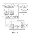
- FIG. 2is a block diagram providing additional details of the ISP circuit 111 coupled to a converter 210 and a denoising filter 214 implemented according to an exemplary embodiment.
- the converter 210illustrates an exemplary embodiment of the converter 119 and the denoising filter 214 illustrates and exemplary embodiment of the denoising filter 113 .
- the GAI informationis provided to an input of a color processing circuit 201 and to an input of an RGB statistics circuit 203 .
- the color processor circuit 201incorporates various color processing functions, such as, for example, a demosaicing function, gamma color correction, color space conversion (CSC), etc.
- the demosaicing functioninterpolates the RG and GB components into RGB components or pixels as understood by those skilled in the art.
- the color space conversionconverts the RGB components into luma (Y) and chrominance (UV) components.
- the luma component Yis provided to a luminance histogram circuit 207
- the YUV componentsare provided to remaining ISP circuitry 205 for further ISP processing as understood by those skilled in the art.
- the remaining ISP circuitry 205provides the processed image to the input of the denoising filter 214 .
- the RGB statistics circuit 203determines average values, minimum values, maximum values, etc. of the RGB color components of the GAI information and provides statistical information ST to an input of an automatic white balance and automatic exposure control (AWB/AEC) circuit 209 .
- AVB/AECautomatic white balance and automatic exposure control
- the luminance histogram circuit 207determines and provides light intensity (LI) information to another input of the AWB/AEC circuit 209 .
- the LI informationis in the form of a luminance histogram which identifies the number of pixels or components at each of a spectrum of light intensity levels.
- the AWB/AEC circuit 209uses the RGB statistics ST and the LI information to calculate appropriate values for the integration time and individual gain values of the gain information GI.
- the AWB/AEC circuit 209updates the integration time and the analog and digital gain components stored within the memory 117 , which outputs the updated integration time to the image sensor 103 , and which outputs the gain information GI to the analog and digital gain circuits 105 and 109 , and the converter 210 as previously described.
- the gain information GIis provided to an index circuit 212 which converts the gain information GI received from the ISP 111 to the total gain value G T .
- the gain value GTis used as an index provided to an input of a lookup table 211 storing noise characteristic estimates or gamma ( ⁇ ) values and corresponding SEL values.
- the total gain G Tis determined from these values and used as an index to map to the corresponding gamma value.
- the index circuit 212may be implemented in any of many different ways. In one embodiment, for example, the index circuit 212 calculates the individual component gain values according to the equations 1-4, averages the green gain values according to equation (5), and then calculates the total gain according to equation (6).
- the selected gamma value ⁇is provided to one input of a threshold circuit 213 which receives the subband size N at another input and which provides the threshold value TH at its output.
- the converter 119is a lookup table directly mapping the gain information GI to the threshold values in which the subband size N is used as part of the input index rather than to a separate threshold circuit.
- the denoising filter 214is implemented as a wavelet-based denoising filter including a forward discrete wavelet transform filter 215 , a threshold application circuit 217 , and a inverse discrete wavelet transform filter 219 .
- the processed imageis provided to an input of the forward discrete wavelet transform filter 215 , which receives the subband size N via another input and which outputs a series of wavelet (W) values collectively forming a wavelet transform representation of the processed image.
- the wavelet values Ware provided to an input of the threshold application circuit 217 , which receives the threshold value TH via another input and which provides adjusted wavelet values AW to an input of the inverse discrete wavelet transform filter 219 .
- the inverse discrete wavelet transform filter 219converts the adjusted wavelet values AW into the low lux filtered image.
- the threshold application circuit 217replaces each of the wavelet values AW that are less than the threshold value TH with a corresponding zero (0) value.
- the wavelet values W that are equal to or greater than the threshold value THpass through the threshold application circuit 217 unmodified.
- the forward and inverse discrete wavelet transformscan be implemented as separable transforms, or as 2-Dimensional transformation, or as a filter bank.
- FIG. 3shows a table 300 mapping the light levels (lux), the individual color component values G R , G Gr , G Gb , and G B , and the corresponding total gain G T with the corresponding gamma value ⁇ and select SEL values.
- the amount of gammais empirically determined at each of different light levels. The total gain calculation is then used to determine the corresponding location within the table 300 . In one embodiment, if the actual determined total gain value falls between values in the table, the actual gamma value may be determined by interpolation. For example, if the total gain is about 19, then the gamma value is about 4.
- the gamma valueis one (1) and denoise filtering is bypassed.
- the SEL value for 300 lux or moreis “0” indicating selection of the processed image rather than the filtered image.
- the gamma valueis greater than one and denoise filtering is selected.
- the SEL value for light level less than 300 luxis “1” so that the filtered image is selected.
- subband size Nmay be incorporated into the table 300 and that gain may also be mapped directly to the threshold value rather than to gamma values.
- the index circuit 212may be incorporated into the gamma conversion circuit 403 providing a direct conversion between the gain information GI and the gamma value ⁇ .
- the gamma ⁇is provided to the threshold circuit 213 to determine the corresponding threshold value TH.
- the conversion circuit 119may be implemented as an arithmetic calculation circuit which converts the gain information GI directly to the gamma value ⁇ and which converts the gamma value ⁇ into the corresponding threshold value TH based on the provided subband size N.
- Lhas a value of approximately 6.71.
- the converter 401has the advantage of replacing the memory circuitry implementing the lookup table 211 with a relatively simple arithmetic calculation circuit.
- An image processing systemincludes an image processor, a converter and a filter.
- the image processorreceives first image information, processes the first image information into second image information, and extracts gain information from the first image information.
- the converterconverts the gain information into a filter threshold.
- the filterfilters the second image information using the filter threshold to provide filtered image information.
- the gain informationis indicative of the amount of illumination of the first image information and thus the noise level of the input image.
- the gain informationmay include analog and digital gain information.
- the convertermay further provide a select value based on the gain information, where the select value is used to select between the second image information and the filtered image information.
- the second image informationmay be selected when the gain information indicates sufficient illumination.
- the convertermay be a lookup table storing a filter threshold values based on the gain information.
- the convertermay alternatively be a lookup table storing a noise characteristic estimates based on the gain information and a threshold circuit.
- the threshold circuitmultiplies a selected noise characteristic estimate from the lookup table by a multiple based on a subband size to provide the filter threshold.
- the convertermay alternatively be an arithmetic calculation circuit which converts the gain information into a total gain, and which converts the total gain into a noise characteristic estimate. Alternatively, the arithmetic calculation circuit may directly convert to the filter threshold.
- the filtermay be a wavelet-based denoising filter.
- the filterincludes a forward discrete wavelet transform filter, a threshold circuit, and an inverse discrete wavelet transform filter.
- the forward discrete wavelet transform filterprovides wavelet values
- the threshold circuitreceives the wavelet values and provides adjusted wavelet values
- the inverse discrete wavelet transform filterreceives the adjusted wavelet values and provides the filtered image information.
- a method of processing image informationincludes processing first image information into second image information, determining gain information from the first image information during processing, converting the gain information into a filter threshold, and filtering the second image information using the filter threshold to provide filtered image information.
- the methodmay include selecting the filtered image information when the gain information indicates an illumination level below a predetermined illumination threshold, and selecting the second image information when the gain information indicates an illumination level above the predetermined threshold.
- the methodmay include providing the gain information to a lookup table storing filter thresholds.
- the methodmay include providing the gain information to a lookup table storing gamma values, and determining the filter threshold based on a selected gamma value and a subband size.
- the methodmay include determining a total gain value from the gain information and converting the total gain value into a gamma value.
- the methodmay include transforming the second image information into wavelet values, replacing wavelet values less than the filter threshold with a zero value and otherwise passing the wavelet values to provide adjusted wavelet values, and transforming the adjusted wavelet values into the filtered image information.
Landscapes
- Engineering & Computer Science (AREA)
- Multimedia (AREA)
- Signal Processing (AREA)
- Image Processing (AREA)
Abstract
Description
GR=GRA*GRD, (1)
a gain value for blue components according to the following equation (2):
GB=GBA*GBD, (2)
a gain value for green components in red rows according to the following equation (3):
GGr=GGrA*GGrD, (3)
and a gain value for green components in blue rows according to the following equation (4):
GGb=GGbA*GGbD, (4)
in which an asterisk “*” denotes multiplication. In one embodiment, the separate green components GGrand GGbare averaged to provide a general gain value for green components in the image according to the following equation (5):
GG=(GGr+GGb)/2 (5)
The gain values GR, GB, and GGmay then be used to determine a total gain value GTaccording to the following equation (6):
GT=(77*GR+150*GG+29*GB) (6)
The total gain GTis associated with the conversion to luma components (Y) as noted below in which the individual color components are weighted relative to each other. The coefficients 77, 150, and 29 are exemplary only and other coefficients may be used depending upon various factors, such as the particular implementation, equipment, data sensors, input image format, etc.
γ=f{GGr,GGb,GB,GR} (7)
As noted above, the total gain GTis determined from these values and used as an index to map to the corresponding gamma value. The
TH=γ√{square root over (2 log2N)} (8)
in which the square-root function is the Donoho threshold value understood by those skilled in the art and N in the subband size as previously described. In an alternative embodiment, the
Claims (20)
Priority Applications (1)
| Application Number | Priority Date | Filing Date | Title |
|---|---|---|---|
| US12/194,697US8339474B2 (en) | 2008-08-20 | 2008-08-20 | Gain controlled threshold in denoising filter for image signal processing |
Applications Claiming Priority (1)
| Application Number | Priority Date | Filing Date | Title |
|---|---|---|---|
| US12/194,697US8339474B2 (en) | 2008-08-20 | 2008-08-20 | Gain controlled threshold in denoising filter for image signal processing |
Publications (2)
| Publication Number | Publication Date |
|---|---|
| US20100045820A1 US20100045820A1 (en) | 2010-02-25 |
| US8339474B2true US8339474B2 (en) | 2012-12-25 |
Family
ID=41696008
Family Applications (1)
| Application Number | Title | Priority Date | Filing Date |
|---|---|---|---|
| US12/194,697Expired - Fee RelatedUS8339474B2 (en) | 2008-08-20 | 2008-08-20 | Gain controlled threshold in denoising filter for image signal processing |
Country Status (1)
| Country | Link |
|---|---|
| US (1) | US8339474B2 (en) |
Cited By (1)
| Publication number | Priority date | Publication date | Assignee | Title |
|---|---|---|---|---|
| US20160071252A1 (en)* | 2014-09-04 | 2016-03-10 | Dong-Hoon Kim | Image processing device, image processing system and method for image processing |
Families Citing this family (10)
| Publication number | Priority date | Publication date | Assignee | Title |
|---|---|---|---|---|
| US8436914B2 (en)* | 2008-11-07 | 2013-05-07 | Cisco Technology, Inc. | Method for automatic exposure control within a video capture device |
| US7978231B2 (en)* | 2008-11-07 | 2011-07-12 | Cisco Technology, Inc. | Method for automatic exposure control within a video capture device |
| JP5419659B2 (en)* | 2009-12-04 | 2014-02-19 | キヤノン株式会社 | Imaging device |
| KR101669819B1 (en) | 2010-11-11 | 2016-10-27 | 삼성전자주식회사 | Filtering apparatus and method for processing depth image for high precision restoration |
| CN105659582B (en)* | 2013-10-31 | 2020-03-27 | 富士胶片株式会社 | Signal processing device, imaging device, parameter generation method, and signal processing method |
| CN104504652A (en)* | 2014-10-10 | 2015-04-08 | 中国人民解放军理工大学 | Image denoising method capable of quickly and effectively retaining edge and directional characteristics |
| US10861127B1 (en) | 2019-09-17 | 2020-12-08 | Gopro, Inc. | Image and video processing using multiple pipelines |
| JP2022183102A (en)* | 2021-05-28 | 2022-12-08 | 三星電子株式会社 | Image sensor including image signal processor and method of operation thereof |
| CN113487522A (en)* | 2021-09-08 | 2021-10-08 | 深圳市诚识科技有限公司 | Multi-channel switching noise reduction method for image communication |
| CN117351216B (en)* | 2023-12-05 | 2024-02-02 | 成都宜图智享信息科技有限公司 | Image self-adaptive denoising method based on supervised deep learning |
Citations (9)
| Publication number | Priority date | Publication date | Assignee | Title |
|---|---|---|---|---|
| US3971065A (en) | 1975-03-05 | 1976-07-20 | Eastman Kodak Company | Color imaging array |
| US5530474A (en)* | 1991-09-05 | 1996-06-25 | Canon Kabushiki Kaisha | White balance correction device with correction signal limiting device |
| US20020027604A1 (en)* | 1999-12-20 | 2002-03-07 | Ching-Yu Hung | Digital still camera system and method |
| US20040234153A1 (en)* | 2001-09-11 | 2004-11-25 | Yoshihiro Nakami | Image processing using object information |
| US20050036707A1 (en)* | 2000-11-09 | 2005-02-17 | Canon Kabushiki Kaisha | Image processing apparatus and its method, program and storage medium |
| US7136095B2 (en) | 2002-06-03 | 2006-11-14 | Sharp Laboratories Of America, Inc. | Digital image system and method for noise compensation |
| US7206455B1 (en)* | 2003-08-20 | 2007-04-17 | Eastman Kodak Company | Adaptive setting of wavelet sub-band thresholds for low-light image denoising |
| US20080225147A1 (en)* | 2003-10-31 | 2008-09-18 | Masumi Dakemoto | Image Pickup Apparatus |
| US20100328544A1 (en)* | 2009-06-29 | 2010-12-30 | Alan Hendrickson | Digital Signal Processor (DSP) Architecture For A Hybrid Television Tuner |
Family Cites Families (21)
| Publication number | Priority date | Publication date | Assignee | Title |
|---|---|---|---|---|
| US5199165A (en)* | 1991-12-13 | 1993-04-06 | Hewlett-Packard Company | Heat pipe-electrical interconnect integration method for chip modules |
| US5579207A (en)* | 1994-10-20 | 1996-11-26 | Hughes Electronics | Three-dimensional integrated circuit stacking |
| US6088227A (en)* | 1995-06-07 | 2000-07-11 | Smiths Industries Aerospace And Defense Systems, Inc. | Heat sink with integrated buss bar |
| SE511425C2 (en)* | 1996-12-19 | 1999-09-27 | Ericsson Telefon Ab L M | Packing device for integrated circuits |
| US6351393B1 (en)* | 1999-07-02 | 2002-02-26 | International Business Machines Corporation | Electronic package for electronic components and method of making same |
| US6215681B1 (en)* | 1999-11-09 | 2001-04-10 | Agile Systems Inc. | Bus bar heat sink |
| JP4608763B2 (en)* | 2000-11-09 | 2011-01-12 | 日本電気株式会社 | Semiconductor device |
| US6800930B2 (en)* | 2002-07-31 | 2004-10-05 | Micron Technology, Inc. | Semiconductor dice having back side redistribution layer accessed using through-silicon vias, and assemblies |
| US7012414B1 (en)* | 2004-08-19 | 2006-03-14 | Coldwatt, Inc. | Vertically packaged switched-mode power converter |
| US7419852B2 (en)* | 2004-08-27 | 2008-09-02 | Micron Technology, Inc. | Low temperature methods of forming back side redistribution layers in association with through wafer interconnects, semiconductor devices including same, and assemblies |
| US7271482B2 (en)* | 2004-12-30 | 2007-09-18 | Micron Technology, Inc. | Methods for forming interconnects in microelectronic workpieces and microelectronic workpieces formed using such methods |
| TW200820402A (en)* | 2006-10-26 | 2008-05-01 | Chipmos Technologies Inc | Stacked chip packaging with heat sink struct |
| US20080284037A1 (en)* | 2007-05-15 | 2008-11-20 | Andry Paul S | Apparatus and Methods for Constructing Semiconductor Chip Packages with Silicon Space Transformer Carriers |
| US8586465B2 (en)* | 2007-06-07 | 2013-11-19 | United Test And Assembly Center Ltd | Through silicon via dies and packages |
| US7592697B2 (en)* | 2007-08-27 | 2009-09-22 | Intel Corporation | Microelectronic package and method of cooling same |
| US20090057867A1 (en)* | 2007-08-30 | 2009-03-05 | Vincent Hool | Integrated Circuit Package with Passive Component |
| US8106505B2 (en)* | 2007-10-31 | 2012-01-31 | International Business Machines Corporation | Assembly including plural through wafer vias, method of cooling the assembly and method of fabricating the assembly |
| US8110415B2 (en)* | 2008-04-03 | 2012-02-07 | International Business Machines Corporation | Silicon based microchannel cooling and electrical package |
| US7939945B2 (en)* | 2008-04-30 | 2011-05-10 | Intel Corporation | Electrically conductive fluid interconnects for integrated circuit devices |
| KR101025013B1 (en)* | 2008-08-20 | 2011-03-25 | 한국전자통신연구원 | Manufacturing method of laminated package with improved through via formation method |
| JP5357510B2 (en)* | 2008-10-31 | 2013-12-04 | 株式会社日立製作所 | Semiconductor integrated circuit device |
- 2008
- 2008-08-20USUS12/194,697patent/US8339474B2/ennot_activeExpired - Fee Related
Patent Citations (9)
| Publication number | Priority date | Publication date | Assignee | Title |
|---|---|---|---|---|
| US3971065A (en) | 1975-03-05 | 1976-07-20 | Eastman Kodak Company | Color imaging array |
| US5530474A (en)* | 1991-09-05 | 1996-06-25 | Canon Kabushiki Kaisha | White balance correction device with correction signal limiting device |
| US20020027604A1 (en)* | 1999-12-20 | 2002-03-07 | Ching-Yu Hung | Digital still camera system and method |
| US20050036707A1 (en)* | 2000-11-09 | 2005-02-17 | Canon Kabushiki Kaisha | Image processing apparatus and its method, program and storage medium |
| US20040234153A1 (en)* | 2001-09-11 | 2004-11-25 | Yoshihiro Nakami | Image processing using object information |
| US7136095B2 (en) | 2002-06-03 | 2006-11-14 | Sharp Laboratories Of America, Inc. | Digital image system and method for noise compensation |
| US7206455B1 (en)* | 2003-08-20 | 2007-04-17 | Eastman Kodak Company | Adaptive setting of wavelet sub-band thresholds for low-light image denoising |
| US20080225147A1 (en)* | 2003-10-31 | 2008-09-18 | Masumi Dakemoto | Image Pickup Apparatus |
| US20100328544A1 (en)* | 2009-06-29 | 2010-12-30 | Alan Hendrickson | Digital Signal Processor (DSP) Architecture For A Hybrid Television Tuner |
Cited By (2)
| Publication number | Priority date | Publication date | Assignee | Title |
|---|---|---|---|---|
| US20160071252A1 (en)* | 2014-09-04 | 2016-03-10 | Dong-Hoon Kim | Image processing device, image processing system and method for image processing |
| US9595086B2 (en)* | 2014-09-04 | 2017-03-14 | Samsung Electronics Co., Ltd. | Image processing device, image processing system and method for image processing |
Also Published As
| Publication number | Publication date |
|---|---|
| US20100045820A1 (en) | 2010-02-25 |
Similar Documents
| Publication | Publication Date | Title |
|---|---|---|
| US8339474B2 (en) | Gain controlled threshold in denoising filter for image signal processing | |
| US7102669B2 (en) | Digital color image pre-processing | |
| US8471932B2 (en) | Spatial filtering for image signal processing | |
| US8743233B2 (en) | Sensitivity-settable image capture apparatus | |
| EP3308534A1 (en) | Color filter array scaler | |
| CN102170530B (en) | Signal processing device and method, solid image capture device and electronic information device | |
| US8154629B2 (en) | Noise canceling circuit, noise canceling method, and solid-state imaging device | |
| EP1987666A2 (en) | Adaptive image filter for filtering image information | |
| US20130329004A1 (en) | Method of and Apparatus for Image Enhancement | |
| US8411943B2 (en) | Method and apparatus for image signal color correction with reduced noise | |
| WO2019104047A1 (en) | Global tone mapping | |
| US7538808B2 (en) | Method and system for luminance noise filtering | |
| US8189066B2 (en) | Image processing apparatus, image processing method, and computer-readable medium | |
| JP4678218B2 (en) | Imaging apparatus and image processing method | |
| US20130114895A1 (en) | Joint Color Channel Image Noise Filtering and Edge Enhancement in the Bayer Domain | |
| JP7491998B2 (en) | Adaptive image data linearization for HDR image sensors - Patents.com | |
| JP5743918B2 (en) | Image processing device | |
| JP2008124653A (en) | Image signal processing apparatus, image signal processing program, and image signal processing method | |
| JP6047686B2 (en) | Imaging device | |
| US20080292209A1 (en) | Dynamic Range Compensation-Dependent Noise Reduction | |
| JP4797949B2 (en) | Imaging apparatus, image processing apparatus, method, and program | |
| JP2015139082A (en) | Image processing apparatus, image processing method, program, and electronic apparatus | |
| US8755622B2 (en) | Image processing apparatus, image processing method, and program | |
| JP2004048562A (en) | Noise reduction circuit and imaging apparatus | |
| WO2016200480A1 (en) | Color filter array scaler |
Legal Events
| Date | Code | Title | Description |
|---|---|---|---|
| AS | Assignment | Owner name:FREESCALE SEMICONDUCTOR, INC.,TEXAS Free format text:ASSIGNMENT OF ASSIGNORS INTEREST;ASSIGNORS:PRIETO, YOLANDA;SAKAUYE, MILES A.;YAN, YONG;AND OTHERS;SIGNING DATES FROM 20080808 TO 20080814;REEL/FRAME:021415/0634 Owner name:FREESCALE SEMICONDUCTOR, INC., TEXAS Free format text:ASSIGNMENT OF ASSIGNORS INTEREST;ASSIGNORS:PRIETO, YOLANDA;SAKAUYE, MILES A.;YAN, YONG;AND OTHERS;SIGNING DATES FROM 20080808 TO 20080814;REEL/FRAME:021415/0634 | |
| AS | Assignment | Owner name:CITIBANK, N.A.,NEW YORK Free format text:SECURITY AGREEMENT;ASSIGNOR:FREESCALE SEMICONDUCTOR, INC.;REEL/FRAME:021936/0772 Effective date:20081107 Owner name:CITIBANK, N.A., NEW YORK Free format text:SECURITY AGREEMENT;ASSIGNOR:FREESCALE SEMICONDUCTOR, INC.;REEL/FRAME:021936/0772 Effective date:20081107 | |
| AS | Assignment | Owner name:CITIBANK, N.A., AS COLLATERAL AGENT,NEW YORK Free format text:SECURITY AGREEMENT;ASSIGNOR:FREESCALE SEMICONDUCTOR, INC.;REEL/FRAME:024397/0001 Effective date:20100413 Owner name:CITIBANK, N.A., AS COLLATERAL AGENT, NEW YORK Free format text:SECURITY AGREEMENT;ASSIGNOR:FREESCALE SEMICONDUCTOR, INC.;REEL/FRAME:024397/0001 Effective date:20100413 | |
| FEPP | Fee payment procedure | Free format text:PAYOR NUMBER ASSIGNED (ORIGINAL EVENT CODE: ASPN); ENTITY STATUS OF PATENT OWNER: LARGE ENTITY | |
| STCF | Information on status: patent grant | Free format text:PATENTED CASE | |
| AS | Assignment | Owner name:CITIBANK, N.A., AS NOTES COLLATERAL AGENT, NEW YORK Free format text:SECURITY AGREEMENT;ASSIGNOR:FREESCALE SEMICONDUCTOR, INC.;REEL/FRAME:030633/0424 Effective date:20130521 Owner name:CITIBANK, N.A., AS NOTES COLLATERAL AGENT, NEW YOR Free format text:SECURITY AGREEMENT;ASSIGNOR:FREESCALE SEMICONDUCTOR, INC.;REEL/FRAME:030633/0424 Effective date:20130521 | |
| AS | Assignment | Owner name:CITIBANK, N.A., AS NOTES COLLATERAL AGENT, NEW YORK Free format text:SECURITY AGREEMENT;ASSIGNOR:FREESCALE SEMICONDUCTOR, INC.;REEL/FRAME:031591/0266 Effective date:20131101 Owner name:CITIBANK, N.A., AS NOTES COLLATERAL AGENT, NEW YOR Free format text:SECURITY AGREEMENT;ASSIGNOR:FREESCALE SEMICONDUCTOR, INC.;REEL/FRAME:031591/0266 Effective date:20131101 | |
| AS | Assignment | Owner name:FREESCALE SEMICONDUCTOR, INC., TEXAS Free format text:PATENT RELEASE;ASSIGNOR:CITIBANK, N.A., AS COLLATERAL AGENT;REEL/FRAME:037354/0757 Effective date:20151207 Owner name:FREESCALE SEMICONDUCTOR, INC., TEXAS Free format text:PATENT RELEASE;ASSIGNOR:CITIBANK, N.A., AS COLLATERAL AGENT;REEL/FRAME:037356/0553 Effective date:20151207 | |
| AS | Assignment | Owner name:MORGAN STANLEY SENIOR FUNDING, INC., MARYLAND Free format text:ASSIGNMENT AND ASSUMPTION OF SECURITY INTEREST IN PATENTS;ASSIGNOR:CITIBANK, N.A.;REEL/FRAME:037486/0517 Effective date:20151207 | |
| AS | Assignment | Owner name:MORGAN STANLEY SENIOR FUNDING, INC., MARYLAND Free format text:ASSIGNMENT AND ASSUMPTION OF SECURITY INTEREST IN PATENTS;ASSIGNOR:CITIBANK, N.A.;REEL/FRAME:037518/0292 Effective date:20151207 | |
| AS | Assignment | Owner name:NORTH STAR INNOVATIONS INC., CALIFORNIA Free format text:ASSIGNMENT OF ASSIGNORS INTEREST;ASSIGNOR:FREESCALE SEMICONDUCTOR, INC.;REEL/FRAME:037694/0264 Effective date:20151002 | |
| AS | Assignment | Owner name:MORGAN STANLEY SENIOR FUNDING, INC., MARYLAND Free format text:SECURITY AGREEMENT SUPPLEMENT;ASSIGNOR:NXP B.V.;REEL/FRAME:038017/0058 Effective date:20160218 | |
| FPAY | Fee payment | Year of fee payment:4 | |
| AS | Assignment | Owner name:MORGAN STANLEY SENIOR FUNDING, INC., MARYLAND Free format text:CORRECTIVE ASSIGNMENT TO CORRECT THE REMOVE APPLICATION 12092129 PREVIOUSLY RECORDED ON REEL 038017 FRAME 0058. ASSIGNOR(S) HEREBY CONFIRMS THE SECURITY AGREEMENT SUPPLEMENT;ASSIGNOR:NXP B.V.;REEL/FRAME:039361/0212 Effective date:20160218 | |
| AS | Assignment | Owner name:NXP B.V., NETHERLANDS Free format text:PATENT RELEASE;ASSIGNOR:MORGAN STANLEY SENIOR FUNDING, INC.;REEL/FRAME:039707/0471 Effective date:20160805 | |
| AS | Assignment | Owner name:NXP, B.V., F/K/A FREESCALE SEMICONDUCTOR, INC., NETHERLANDS Free format text:RELEASE BY SECURED PARTY;ASSIGNOR:MORGAN STANLEY SENIOR FUNDING, INC.;REEL/FRAME:040925/0001 Effective date:20160912 Owner name:NXP, B.V., F/K/A FREESCALE SEMICONDUCTOR, INC., NE Free format text:RELEASE BY SECURED PARTY;ASSIGNOR:MORGAN STANLEY SENIOR FUNDING, INC.;REEL/FRAME:040925/0001 Effective date:20160912 | |
| AS | Assignment | Owner name:NXP B.V., NETHERLANDS Free format text:RELEASE BY SECURED PARTY;ASSIGNOR:MORGAN STANLEY SENIOR FUNDING, INC.;REEL/FRAME:040928/0001 Effective date:20160622 | |
| AS | Assignment | Owner name:MORGAN STANLEY SENIOR FUNDING, INC., MARYLAND Free format text:CORRECTIVE ASSIGNMENT TO CORRECT THE REMOVE PATENTS 8108266 AND 8062324 AND REPLACE THEM WITH 6108266 AND 8060324 PREVIOUSLY RECORDED ON REEL 037518 FRAME 0292. ASSIGNOR(S) HEREBY CONFIRMS THE ASSIGNMENT AND ASSUMPTION OF SECURITY INTEREST IN PATENTS;ASSIGNOR:CITIBANK, N.A.;REEL/FRAME:041703/0536 Effective date:20151207 | |
| AS | Assignment | Owner name:MORGAN STANLEY SENIOR FUNDING, INC., MARYLAND Free format text:CORRECTIVE ASSIGNMENT TO CORRECT THE REMOVE APPLICATION 12681366 PREVIOUSLY RECORDED ON REEL 039361 FRAME 0212. ASSIGNOR(S) HEREBY CONFIRMS THE SECURITY AGREEMENT SUPPLEMENT;ASSIGNOR:NXP B.V.;REEL/FRAME:042762/0145 Effective date:20160218 Owner name:MORGAN STANLEY SENIOR FUNDING, INC., MARYLAND Free format text:CORRECTIVE ASSIGNMENT TO CORRECT THE REMOVE APPLICATION 12681366 PREVIOUSLY RECORDED ON REEL 038017 FRAME 0058. ASSIGNOR(S) HEREBY CONFIRMS THE SECURITY AGREEMENT SUPPLEMENT;ASSIGNOR:NXP B.V.;REEL/FRAME:042985/0001 Effective date:20160218 | |
| AS | Assignment | Owner name:SHENZHEN XINGUODU TECHNOLOGY CO., LTD., CHINA Free format text:CORRECTIVE ASSIGNMENT TO CORRECT THE TO CORRECT THE APPLICATION NO. FROM 13,883,290 TO 13,833,290 PREVIOUSLY RECORDED ON REEL 041703 FRAME 0536. ASSIGNOR(S) HEREBY CONFIRMS THE THE ASSIGNMENT AND ASSUMPTION OF SECURITYINTEREST IN PATENTS.;ASSIGNOR:MORGAN STANLEY SENIOR FUNDING, INC.;REEL/FRAME:048734/0001 Effective date:20190217 | |
| AS | Assignment | Owner name:NXP B.V., NETHERLANDS Free format text:RELEASE BY SECURED PARTY;ASSIGNOR:MORGAN STANLEY SENIOR FUNDING, INC.;REEL/FRAME:050745/0001 Effective date:20190903 | |
| AS | Assignment | Owner name:MORGAN STANLEY SENIOR FUNDING, INC., MARYLAND Free format text:CORRECTIVE ASSIGNMENT TO CORRECT THE REMOVE APPLICATION 12298143 PREVIOUSLY RECORDED ON REEL 042985 FRAME 0001. ASSIGNOR(S) HEREBY CONFIRMS THE SECURITY AGREEMENT SUPPLEMENT;ASSIGNOR:NXP B.V.;REEL/FRAME:051029/0001 Effective date:20160218 Owner name:MORGAN STANLEY SENIOR FUNDING, INC., MARYLAND Free format text:CORRECTIVE ASSIGNMENT TO CORRECT THE REMOVE APPLICATION 12298143 PREVIOUSLY RECORDED ON REEL 042762 FRAME 0145. ASSIGNOR(S) HEREBY CONFIRMS THE SECURITY AGREEMENT SUPPLEMENT;ASSIGNOR:NXP B.V.;REEL/FRAME:051145/0184 Effective date:20160218 Owner name:MORGAN STANLEY SENIOR FUNDING, INC., MARYLAND Free format text:CORRECTIVE ASSIGNMENT TO CORRECT THE REMOVE APPLICATION 12298143 PREVIOUSLY RECORDED ON REEL 039361 FRAME 0212. ASSIGNOR(S) HEREBY CONFIRMS THE SECURITY AGREEMENT SUPPLEMENT;ASSIGNOR:NXP B.V.;REEL/FRAME:051029/0387 Effective date:20160218 Owner name:MORGAN STANLEY SENIOR FUNDING, INC., MARYLAND Free format text:CORRECTIVE ASSIGNMENT TO CORRECT THE REMOVE APPLICATION12298143 PREVIOUSLY RECORDED ON REEL 042985 FRAME 0001. ASSIGNOR(S) HEREBY CONFIRMS THE SECURITY AGREEMENT SUPPLEMENT;ASSIGNOR:NXP B.V.;REEL/FRAME:051029/0001 Effective date:20160218 Owner name:MORGAN STANLEY SENIOR FUNDING, INC., MARYLAND Free format text:CORRECTIVE ASSIGNMENT TO CORRECT THE REMOVE APPLICATION12298143 PREVIOUSLY RECORDED ON REEL 039361 FRAME 0212. ASSIGNOR(S) HEREBY CONFIRMS THE SECURITY AGREEMENT SUPPLEMENT;ASSIGNOR:NXP B.V.;REEL/FRAME:051029/0387 Effective date:20160218 Owner name:MORGAN STANLEY SENIOR FUNDING, INC., MARYLAND Free format text:CORRECTIVE ASSIGNMENT TO CORRECT THE REMOVE APPLICATION 12298143 PREVIOUSLY RECORDED ON REEL 038017 FRAME 0058. ASSIGNOR(S) HEREBY CONFIRMS THE SECURITY AGREEMENT SUPPLEMENT;ASSIGNOR:NXP B.V.;REEL/FRAME:051030/0001 Effective date:20160218 Owner name:MORGAN STANLEY SENIOR FUNDING, INC., MARYLAND Free format text:CORRECTIVE ASSIGNMENT TO CORRECT THE REMOVE APPLICATION12298143 PREVIOUSLY RECORDED ON REEL 042762 FRAME 0145. ASSIGNOR(S) HEREBY CONFIRMS THE SECURITY AGREEMENT SUPPLEMENT;ASSIGNOR:NXP B.V.;REEL/FRAME:051145/0184 Effective date:20160218 | |
| AS | Assignment | Owner name:MORGAN STANLEY SENIOR FUNDING, INC., MARYLAND Free format text:CORRECTIVE ASSIGNMENT TO CORRECT THE REMOVE APPLICATION11759915 AND REPLACE IT WITH APPLICATION 11759935 PREVIOUSLY RECORDED ON REEL 037486 FRAME 0517. ASSIGNOR(S) HEREBY CONFIRMS THE ASSIGNMENT AND ASSUMPTION OF SECURITYINTEREST IN PATENTS;ASSIGNOR:CITIBANK, N.A.;REEL/FRAME:053547/0421 Effective date:20151207 | |
| AS | Assignment | Owner name:NXP B.V., NETHERLANDS Free format text:CORRECTIVE ASSIGNMENT TO CORRECT THE REMOVEAPPLICATION 11759915 AND REPLACE IT WITH APPLICATION11759935 PREVIOUSLY RECORDED ON REEL 040928 FRAME 0001. ASSIGNOR(S) HEREBY CONFIRMS THE RELEASE OF SECURITYINTEREST;ASSIGNOR:MORGAN STANLEY SENIOR FUNDING, INC.;REEL/FRAME:052915/0001 Effective date:20160622 | |
| AS | Assignment | Owner name:NXP, B.V. F/K/A FREESCALE SEMICONDUCTOR, INC., NETHERLANDS Free format text:CORRECTIVE ASSIGNMENT TO CORRECT THE REMOVEAPPLICATION 11759915 AND REPLACE IT WITH APPLICATION11759935 PREVIOUSLY RECORDED ON REEL 040925 FRAME 0001. ASSIGNOR(S) HEREBY CONFIRMS THE RELEASE OF SECURITYINTEREST;ASSIGNOR:MORGAN STANLEY SENIOR FUNDING, INC.;REEL/FRAME:052917/0001 Effective date:20160912 | |
| FEPP | Fee payment procedure | Free format text:MAINTENANCE FEE REMINDER MAILED (ORIGINAL EVENT CODE: REM.); ENTITY STATUS OF PATENT OWNER: LARGE ENTITY | |
| LAPS | Lapse for failure to pay maintenance fees | Free format text:PATENT EXPIRED FOR FAILURE TO PAY MAINTENANCE FEES (ORIGINAL EVENT CODE: EXP.); ENTITY STATUS OF PATENT OWNER: LARGE ENTITY | |
| STCH | Information on status: patent discontinuation | Free format text:PATENT EXPIRED DUE TO NONPAYMENT OF MAINTENANCE FEES UNDER 37 CFR 1.362 | |
| FP | Lapsed due to failure to pay maintenance fee | Effective date:20201225 |