US8339102B2 - System and method for regulating loading on an integrated circuit power supply - Google Patents
System and method for regulating loading on an integrated circuit power supplyDownload PDFInfo
- Publication number
- US8339102B2 US8339102B2US10/986,799US98679904AUS8339102B2US 8339102 B2US8339102 B2US 8339102B2US 98679904 AUS98679904 AUS 98679904AUS 8339102 B2US8339102 B2US 8339102B2
- Authority
- US
- United States
- Prior art keywords
- load
- charge pump
- volatile memory
- voltage
- memory device
- Prior art date
- Legal status (The legal status is an assumption and is not a legal conclusion. Google has not performed a legal analysis and makes no representation as to the accuracy of the status listed.)
- Active, expires
Links
Images


Classifications
- G—PHYSICS
- G11—INFORMATION STORAGE
- G11C—STATIC STORES
- G11C5/00—Details of stores covered by group G11C11/00
- G11C5/14—Power supply arrangements, e.g. power down, chip selection or deselection, layout of wirings or power grids, or multiple supply levels
- G11C5/143—Detection of memory cassette insertion or removal; Continuity checks of supply or ground lines; Detection of supply variations, interruptions or levels ; Switching between alternative supplies
- H—ELECTRICITY
- H02—GENERATION; CONVERSION OR DISTRIBUTION OF ELECTRIC POWER
- H02M—APPARATUS FOR CONVERSION BETWEEN AC AND AC, BETWEEN AC AND DC, OR BETWEEN DC AND DC, AND FOR USE WITH MAINS OR SIMILAR POWER SUPPLY SYSTEMS; CONVERSION OF DC OR AC INPUT POWER INTO SURGE OUTPUT POWER; CONTROL OR REGULATION THEREOF
- H02M3/00—Conversion of DC power input into DC power output
- H02M3/02—Conversion of DC power input into DC power output without intermediate conversion into AC
- H02M3/04—Conversion of DC power input into DC power output without intermediate conversion into AC by static converters
- H02M3/06—Conversion of DC power input into DC power output without intermediate conversion into AC by static converters using resistors or capacitors, e.g. potential divider
- H02M3/07—Conversion of DC power input into DC power output without intermediate conversion into AC by static converters using resistors or capacitors, e.g. potential divider using capacitors charged and discharged alternately by semiconductor devices with control electrode, e.g. charge pumps
- H02M3/073—Charge pumps of the Schenkel-type
Definitions
- the present inventionrelates to Voltage/Current sources in general, and more particularly, to a method and apparatus for driving a load or for adjusting a load driven by a voltage or current source.
- Non-volatile memory (“NVM”) arrayssuch as erasable, programmable read only memory (EPROM) or flash memory arrays, or electrically erasable, programmable read only memory (EEPROM) arrays, require high positive or negative voltages to program and erase memory cells of the array. Typically, these voltages are higher than the voltage supplied for other operations (Vdd). Voltage/Current sources are generally used to boost on-chip voltages above the supply voltage Vdd to reach the voltages required for programming or erasing. A charge pump may be used as a voltage/current source.
- a charge pumpmay comprise cascaded stages that progressively boost the output voltage to higher levels.
- the charge pumpmay progressively store an increasing charge on a capacitor that is part of a capacitor-diode combination, with several such stages being placed together in a network to obtain the desired increase in voltage.
- FIG. 1illustrates four stages of a commonly used four-stage charge pump architecture, called a four-phased-clock, threshold-voltage-canceling pump architecture (see Umezawa, IEEE Journal of Solid State Circuits, Vol. 27, 1992, page 1540).
- the charge pump circuitincludes a plurality of charge transfer transistors (reference letters m 1 ) connected in series. In FIG. 1 , four such charge transfer transistors are shown, labeled m 1 , m 2 , m 3 and m 4 .
- Charge transfer transistors m 1may use, but are not limited to, CMOS (complementary metal oxide semiconductor) technology, being either n-channel or p-channel (NMOS or PMOS) field effect transistors (FETs).
- FIG. 1illustrates a positive charge pump based on NMOS.
- voltage/current sourcessuch as charge pumps
- memory devicessuch as EPROM, Flash or EEPROM memory devices
- many memory cellsmay require a high voltage at the same time, for example, to perform program and erase operations.
- the current drawn by the the NVM cellmay vary significantly based on factors such as voltage, temperature, process corners, number of program/erase cycles already passed, etc. If the total current of many NVM cells exceeds the capacity of the voltage/current source, then the voltage/current source may not be able to supply the required voltage to perform the operation of the memory device.
- an appropriate regulation apparatusmay be used to control and provide a desired voltage at the output of the voltage/current source.
- a regulation methodmay be used to enhance the operation of the charge pump. This may be accomplished by using a regulator to regulate the pump output.
- a regulatormay typically adjust the capability of the charge pump according to the required current of the load. Thus, for example, if the current of the load exceeds a maximum value, the regulator may not be able to adjust the charge pump and it may stay in saturation.
- one known method for providing regulation of the output of a charge pumpsuffers from the drawback of current inefficiency.
- the regulated output voltage of charge pump 100which is driven to load 120 is fed into a voltage divider 102 and compared to a reference voltage (Vref) 104 at operational amplifier 106 .
- Vrefreference voltage
- the regulation of the output of charge pump 100is achieved by shunting the output to ground 108 .
- charge pump 100operates at minimum energy, e.g., low Vdd
- the current dissipated through ground 108is, likewise, low.
- charge pump 100operates at higher energy conditions, e.g., high Vdd, current is dissipated through ground 108 , resulting in inefficient operation of the regulating system of FIG. 2 .
- a load adjustment circuitcomprising a power source to supply power to a load and a control unit to control a property of said load, wherein said control unit adjusts said property of the load based on a signal received from said power source.
- a method of adjusting a loadcomprising supplying power to a load and determining whether the power supplied to said load is greater than a maximum threshold and if so, adjusting a property of said load to decrease the power supplied to said load.
- FIG. 1is a simplified circuit diagram of a commonly used charge pump architecture including a four-phased charge pump;
- FIG. 2is a block diagram illustration of a commonly used shunting system for charge pump output voltage regulation
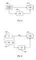
- FIG. 3is a simplified block diagram illustration of an apparatus for adjusting a load in accordance with some embodiments of the present invention
- FIG. 4is a simplified block diagram illustration of a regulated apparatus for adjusting a load in accordance with some embodiments of the present invention.
- FIG. 5is a flow chart illustration of a method to adjust a load, in accordance with some embodiments of the present invention.
- FIG. 3is a simplified block diagram illustration of an apparatus for adjusting a load supplied by a voltage/current source in accordance with some embodiments of the present invention.
- Some embodiments of the present inventionmay include a power source 300 , which power may, for example, be used to boost on-chip voltages above the supply voltage Vdd. In some embodiments, the output of power source 300 may be used to reach voltages required for programming or erasing memory cells.
- the power sourcemay drive a load 310 .
- Control unit 320may adjust a property of load 310 .
- power source 300may be a constant voltage/current source. Control unit 320 may receive signals relating to the power supplied to load 310 and accordingly adjust a property of load 310 to increase or decrease its power consumption.
- the property of the loadmay be its size.
- load 310may be a segmented virtual ground array having connectable cells or groups of cells.
- adjusting the size of the loadmay entail connecting or disconnecting a word line or a bit line within load 310 .
- Other properties of the load being driven that may be adjusted by control unit 320are the output impedance, e.g., the number of connected bit lines, or the number of connected memory cells.
- FIG. 4is a simplified block diagram illustration of a regulated apparatus for adjusting a load in accordance with some embodiments of the present invention.
- control unit 420may generate an overload signal, triggering an adjustment mechanism to adjust a property of load 410 , for example, in order to decrease the power required by the load 410 .
- the maximum thresholdmay, for example, correspond to the maximum voltage that the power source 400 is capable of supplying, thereby avoiding frequent exhaustion of the power source.
- Control unit 420may incrementally adjust one or more properties of load 410 based on such overload signal, until the overload signal is no longer generated.
- regulator 430may operate in conjunction with control unit 420 .
- Regulator 430may regulate the operation of the power source 400 .
- the power sourcemay be adjusted, and in other instances of overload, the load may be adjusted, and in yet other instances, both may be adjusted.
- the choicemay depend on a variety of factors, for example, mode of operation or other operating conditions.
- an overload signalmay be generated, for example, from regulator 430 to control unit 420 .
- the adjustment of loadin accordance with some embodiments of the invention may be performed by using an array architecture described in U.S. Pat. No. 5,963,465 titled “A SYMMETRIC SEGMENTED MEMORY ARRAY ARCHITECTURE”.
- a load unitmay comprise a portion of an area in the array, and therefore, adjusting the load may be performed without adding additional circuitry.
- FIG. 5is a flow chart illustration of a method to adjust a load, in accordance with some embodiments of the present invention.
- the control unitmay set an initial load.
- the control unitmay initially connect the voltage/current source to a minimum number of load units, for example, one load unit, or to a maximum number of load units, for example, the memory array (block 1000 ).
- a load unitmay, for example, be a block or sub-array of memory cells, one or a number of word lines or bit lines, or an individual memory cell.
- the “overload” signalmay not be set, for example, by an overload bit being at a “0” logic level, and the number of load units driven by the power source may be increased (blocks 2000 and 4000 ).
- the “overload” signalmay be set, for example, by adjusted an overload bit to a “1” logic level. In such case, as long as the charge pump is connected to more than one load unit, the amount of load units may be decreased (blocks 5000 and 6000 ). Accordingly, the size of the load may be established (block 7000 ).
- the method of the present inventionmay define an optimal load parameter.
- the optimal load parametermay be the lesser of the total size of the load, for example, all memory cells in an array being driven, or the maximum load that the power source is able to drive simultaneously.
- the optimal load parametermay, for example, be used as a default parameter in the operation of the present invention.
- the optimal powermay be determined every number of cycles of operation of the load or it may be reset when the “overload” signal is set from active to inactive, for example, when an overload bit is changed from “1” to “0”.
- the loadmay be further adjusted due to fabrication parameters such as process corners (e.g. cells with extreme characteristics), temperature changes, Vdd and load current fluctuation.
- the voltage/current source of embodiments of the present inventionmay be any suitable power source, for example, a constant voltage/current source or one or more charge pumps to boost on-chip voltages above the supply voltage Vdd to reach the voltages required for programming or erasing.
- a constant voltage/current source or one or more charge pumpsto boost on-chip voltages above the supply voltage Vdd to reach the voltages required for programming or erasing.
- the present inventionmay be practiced with other Voltage/Current sources in addition to or in place of such one or more charge pumps.
- Some embodiments of the present inventionbenefit from a significant reduction in the on-chip area required for a power source, such as a charge pump, for example, by requiring a reduced number of capacitors to boost voltages above the supply voltage Vdd to reach the voltages required for programming or erasing.
- a power sourcesuch as a charge pump
- the fluctuation of a loadmay be covered by added capacitors to boost the voltage above the supply voltage Vdd.
- the fluctuation of the loadmay be covered by adapting the load to the voltage/current source.
Landscapes
- Engineering & Computer Science (AREA)
- Power Engineering (AREA)
- Dc-Dc Converters (AREA)
- Read Only Memory (AREA)
- Continuous-Control Power Sources That Use Transistors (AREA)
Abstract
Description
Claims (15)
Priority Applications (1)
| Application Number | Priority Date | Filing Date | Title |
|---|---|---|---|
| US10/986,799US8339102B2 (en) | 2004-02-10 | 2004-11-15 | System and method for regulating loading on an integrated circuit power supply |
Applications Claiming Priority (2)
| Application Number | Priority Date | Filing Date | Title |
|---|---|---|---|
| US54287104P | 2004-02-10 | 2004-02-10 | |
| US10/986,799US8339102B2 (en) | 2004-02-10 | 2004-11-15 | System and method for regulating loading on an integrated circuit power supply |
Publications (2)
| Publication Number | Publication Date |
|---|---|
| US20050174709A1 US20050174709A1 (en) | 2005-08-11 |
| US8339102B2true US8339102B2 (en) | 2012-12-25 |
Family
ID=35062388
Family Applications (1)
| Application Number | Title | Priority Date | Filing Date |
|---|---|---|---|
| US10/986,799Active2026-04-13US8339102B2 (en) | 2004-02-10 | 2004-11-15 | System and method for regulating loading on an integrated circuit power supply |
Country Status (2)
| Country | Link |
|---|---|
| US (1) | US8339102B2 (en) |
| DE (1) | DE102005006131A1 (en) |
Cited By (9)
| Publication number | Priority date | Publication date | Assignee | Title |
|---|---|---|---|---|
| US20110221405A1 (en)* | 2010-03-09 | 2011-09-15 | Primarion Inc. | Methods and apparatus for calibration of power converters |
| US10348191B2 (en)* | 2015-11-25 | 2019-07-09 | Psemi Corporation | Switched-capacitor network packaged with load |
| US11901817B2 (en) | 2013-03-15 | 2024-02-13 | Psemi Corporation | Protection of switched capacitor power converter |
| US12107495B2 (en) | 2015-07-08 | 2024-10-01 | Psemi Corporation | Switched-capacitor power converters |
| US12212232B2 (en) | 2013-03-15 | 2025-01-28 | Psemi Corporation | Power supply for gate driver in switched-capacitor circuit |
| US12237765B2 (en) | 2015-03-13 | 2025-02-25 | Psemi Corporation | DC-DC transformer with inductor for the facilitation of adiabatic inter-capacitor charge transport |
| US12341424B2 (en) | 2011-05-05 | 2025-06-24 | Psemi Corporation | Power converters with modular stages |
| US12381482B2 (en) | 2011-05-05 | 2025-08-05 | Psemi Corporation | Power converter with modular stages connected by floating terminals |
| US12438135B2 (en) | 2011-10-18 | 2025-10-07 | Psemi Corporation | Multilayer power, converter with devices having reduced lateral current |
Families Citing this family (2)
| Publication number | Priority date | Publication date | Assignee | Title |
|---|---|---|---|---|
| US9618996B2 (en)* | 2013-09-11 | 2017-04-11 | Electronics And Telecommunications Research Institute | Power capping apparatus and method |
| US20160091950A1 (en)* | 2014-09-26 | 2016-03-31 | Apple Inc. | Peak current management |
Citations (79)
| Publication number | Priority date | Publication date | Assignee | Title |
|---|---|---|---|---|
| US4961010A (en) | 1989-05-19 | 1990-10-02 | National Semiconductor Corporation | Output buffer for reducing switching induced noise |
| US5029063A (en) | 1989-03-25 | 1991-07-02 | Eurosil Electronic Gmbh | MOSFET multiplying circuit |
| US5081371A (en) | 1990-11-07 | 1992-01-14 | U.S. Philips Corp. | Integrated charge pump circuit with back bias voltage reduction |
| US5142495A (en) | 1989-03-10 | 1992-08-25 | Intel Corporation | Variable load for margin mode |
| US5142496A (en) | 1991-06-03 | 1992-08-25 | Advanced Micro Devices, Inc. | Method for measuring VT 's less than zero without applying negative voltages |
| US5276646A (en) | 1990-09-25 | 1994-01-04 | Samsung Electronics Co., Ltd. | High voltage generating circuit for a semiconductor memory circuit |
| US5280420A (en) | 1992-10-02 | 1994-01-18 | National Semiconductor Corporation | Charge pump which operates on a low voltage power supply |
| US5381374A (en) | 1992-01-09 | 1995-01-10 | Kabushiki Kaisha Toshiba | Memory cell data output circuit having improved access time |
| US5422847A (en)* | 1992-03-04 | 1995-06-06 | Kabushiki Kaisha Toshiba | Non-volatile memory controlling apparatus |
| EP0693781A1 (en) | 1994-07-13 | 1996-01-24 | United Microelectronics Corporation | Grounding method for eliminating process antenna effect |
| US5534804A (en) | 1995-02-13 | 1996-07-09 | Advanced Micro Devices, Inc. | CMOS power-on reset circuit using hysteresis |
| US5553030A (en) | 1993-09-10 | 1996-09-03 | Intel Corporation | Method and apparatus for controlling the output voltage provided by a charge pump circuit |
| US5559687A (en) | 1993-06-21 | 1996-09-24 | Sgs-Thomson Microelectronics, S.R.L. | Voltage multiplier for high output current with stabilized output voltage |
| US5581252A (en) | 1994-10-13 | 1996-12-03 | Linear Technology Corporation | Analog-to-digital conversion using comparator coupled capacitor digital-to-analog converters |
| US5612642A (en) | 1995-04-28 | 1997-03-18 | Altera Corporation | Power-on reset circuit with hysteresis |
| US5636288A (en) | 1995-02-16 | 1997-06-03 | Paradigm Electronics Inc. | Standby power circuit arrangement |
| US5663907A (en) | 1996-04-25 | 1997-09-02 | Bright Microelectronics, Inc. | Switch driver circuit for providing small sector sizes for negative gate erase flash EEPROMS using a standard twin-well CMOS process |
| US5672959A (en) | 1996-04-12 | 1997-09-30 | Micro Linear Corporation | Low drop-out voltage regulator having high ripple rejection and low power consumption |
| US5675280A (en) | 1993-06-17 | 1997-10-07 | Fujitsu Limited | Semiconductor integrated circuit device having built-in step-down circuit for stepping down external power supply voltage |
| US5708608A (en) | 1995-12-28 | 1998-01-13 | Hyundai Electronics Industries Cp., Ltd. | High-speed and low-noise output buffer |
| US5717581A (en) | 1994-06-30 | 1998-02-10 | Sgs-Thomson Microelectronics, Inc. | Charge pump circuit with feedback control |
| US5726946A (en) | 1994-06-02 | 1998-03-10 | Mitsubishi Denki Kabushiki Kaisha | Semiconductor integrated circuit device having hierarchical power source arrangement |
| EP0843398A2 (en) | 1996-11-18 | 1998-05-20 | WaferScale Integration Inc. | Backup battery switch |
| US5760634A (en) | 1996-09-12 | 1998-06-02 | United Microelectronics Corporation | High speed, low noise output buffer |
| US5808506A (en) | 1996-10-01 | 1998-09-15 | Information Storage Devices, Inc. | MOS charge pump generation and regulation method and apparatus |
| US5815435A (en) | 1995-10-10 | 1998-09-29 | Information Storage Devices, Inc. | Storage cell for analog recording and playback |
| US5847441A (en) | 1996-05-10 | 1998-12-08 | Micron Technology, Inc. | Semiconductor junction antifuse circuit |
| US5880620A (en) | 1997-04-22 | 1999-03-09 | Xilinx, Inc. | Pass gate circuit with body bias control |
| US5889721A (en)* | 1997-08-21 | 1999-03-30 | Integrated Silicon Solution, Inc. | Method and apparatus for operating functions relating to memory and/or applications that employ memory in accordance with available power |
| US5903031A (en) | 1995-07-04 | 1999-05-11 | Matsushita Electric Industrial Co., Ltd. | MIS device, method of manufacturing the same, and method of diagnosing the same |
| US5910924A (en) | 1996-08-27 | 1999-06-08 | Hitachi, Ltd. | Semiconductor integrated circuit including voltage converter effective at low operational voltages |
| US5946258A (en) | 1998-03-16 | 1999-08-31 | Intel Corporation | Pump supply self regulation for flash memory cell pair reference circuit |
| US5963412A (en) | 1997-11-13 | 1999-10-05 | Advanced Micro Devices, Inc. | Process induced charging damage control device |
| US6005423A (en) | 1994-02-10 | 1999-12-21 | Xilinx, Inc. | Low current power-on reset circuit |
| US6028324A (en) | 1997-03-07 | 2000-02-22 | Taiwan Semiconductor Manufacturing Company | Test structures for monitoring gate oxide defect densities and the plasma antenna effect |
| US6040610A (en) | 1997-04-08 | 2000-03-21 | Kabushiki Kaisha Toshiba | Semiconductor device |
| US6064251A (en) | 1997-08-27 | 2000-05-16 | Integrated Silicon Solution, Inc. | System and method for a low voltage charge pump with large output voltage range |
| US6075402A (en) | 1996-10-11 | 2000-06-13 | Sgs-Thomson Microelectronics S.R.L. | Positive charge pump |
| US6081456A (en) | 1999-02-04 | 2000-06-27 | Tower Semiconductor Ltd. | Bit line control circuit for a memory array using 2-bit non-volatile memory cells |
| US6094095A (en) | 1998-06-29 | 2000-07-25 | Cypress Semiconductor Corp. | Efficient pump for generating voltages above and/or below operating voltages |
| US6107862A (en) | 1997-02-28 | 2000-08-22 | Seiko Instruments Inc. | Charge pump circuit |
| US6118207A (en) | 1997-11-12 | 2000-09-12 | Deka Products Limited Partnership | Piezo-electric actuator operable in an electrolytic fluid |
| US6130574A (en) | 1997-01-24 | 2000-10-10 | Siemens Aktiengesellschaft | Circuit configuration for producing negative voltages, charge pump having at least two circuit configurations and method of operating a charge pump |
| US6130572A (en) | 1997-01-23 | 2000-10-10 | Stmicroelectronics S.R.L. | NMOS negative charge pump |
| US6150800A (en) | 1998-09-16 | 2000-11-21 | Matsushita Electric Industrial Co., Ltd. | Power circuit including inrush current limiter, and integrated circuit including the power circuit |
| US6154081A (en) | 1999-06-15 | 2000-11-28 | Delphi Technologies, Inc. | Load circuit having extended reverse voltage protection |
| US6157242A (en) | 1998-03-19 | 2000-12-05 | Sharp Kabushiki Kaisha | Charge pump for operation at a wide range of power supply voltages |
| US6188211B1 (en) | 1998-05-13 | 2001-02-13 | Texas Instruments Incorporated | Current-efficient low-drop-out voltage regulator with improved load regulation and frequency response |
| US6198342B1 (en) | 1998-12-08 | 2001-03-06 | Sharp Kabushiki Kaisha | Charge pump circuit simple in construction and free from trouble even at low voltage |
| US6208200B1 (en) | 1997-07-14 | 2001-03-27 | Sony Corporation | Level shift circuit with low voltage operation |
| JP2001118392A (en) | 1993-08-27 | 2001-04-27 | Toshiba Corp | Nonvolatile semiconductor memory and data programming method thereof |
| US6246555B1 (en) | 2000-09-06 | 2001-06-12 | Prominenet Communications Inc. | Transient current and voltage protection of a voltage regulator |
| US6285614B1 (en) | 1997-11-21 | 2001-09-04 | Stmicroelectronics S.R.L. | Voltage regulator for single feed voltage memory circuits, and flash type memory in particular |
| US6297974B1 (en) | 1999-09-27 | 2001-10-02 | Intel Corporation | Method and apparatus for reducing stress across capacitors used in integrated circuits |
| US6339556B1 (en) | 1999-11-15 | 2002-01-15 | Nec Corporation | Semiconductor memory device |
| US20020024332A1 (en)* | 2000-06-09 | 2002-02-28 | Gardner Jay Warren | Methods and apparatus for controlling electric appliances during reduced power conditions |
| US6353356B1 (en) | 1999-08-30 | 2002-03-05 | Micron Technology, Inc. | High voltage charge pump circuits |
| US6356469B1 (en) | 2000-09-14 | 2002-03-12 | Fairchild Semiconductor Corporation | Low voltage charge pump employing optimized clock amplitudes |
| US6359501B2 (en) | 2000-02-11 | 2002-03-19 | Windbond Eelctronics Corp. | Charge-pumping circuits for a low-supply voltage |
| US6400209B1 (en) | 1999-08-05 | 2002-06-04 | Fujitsu Limited | Switch circuit with back gate voltage control and series regulator |
| US6433624B1 (en) | 2000-11-30 | 2002-08-13 | Intel Corporation | Threshold voltage generation circuit |
| US6452438B1 (en) | 2000-12-28 | 2002-09-17 | Intel Corporation | Triple well no body effect negative charge pump |
| US20020145483A1 (en)* | 1997-05-27 | 2002-10-10 | Bouisse Gerard Jean Louis | Circuit and method for impedance matching |
| US20020145465A1 (en) | 2001-04-05 | 2002-10-10 | Joseph Shor | Efficient charge pump apparatus and method for operating the same |
| US20020167827A1 (en)* | 2001-01-29 | 2002-11-14 | Hiroyuki Umeda | Power supply apparatus |
| US20030076159A1 (en) | 2001-10-24 | 2003-04-24 | Shor Joseph S. | Stack element circuit |
| US6577514B2 (en) | 2001-04-05 | 2003-06-10 | Saifun Semiconductors Ltd. | Charge pump with constant boosted output voltage |
| US20030107428A1 (en)* | 2001-11-09 | 2003-06-12 | Stmicroelectronics S.R.L. | Low power charge pump circuit |
| US6608526B1 (en) | 2002-04-17 | 2003-08-19 | National Semiconductor Corporation | CMOS assisted output stage |
| US6614295B2 (en) | 2000-12-28 | 2003-09-02 | Nec Corporation | Feedback-type amplifier circuit and driver circuit |
| US6627555B2 (en) | 1999-06-18 | 2003-09-30 | Saifun Semiconductors Ltd. | Method and circuit for minimizing the charging effect during manufacture of semiconductor devices |
| US20030202411A1 (en) | 2002-04-29 | 2003-10-30 | Shigekazu Yamada | System for control of pre-charge levels in a memory device |
| US6654296B2 (en) | 2001-07-23 | 2003-11-25 | Samsung Electronics Co., Ltd. | Devices, circuits and methods for dual voltage generation using single charge pump |
| US6665769B2 (en) | 2001-04-05 | 2003-12-16 | Saifun Semiconductors Ltd. | Method and apparatus for dynamically masking an N-bit memory array having individually programmable cells |
| US6677805B2 (en) | 2001-04-05 | 2004-01-13 | Saifun Semiconductors Ltd. | Charge pump stage with body effect minimization |
| US20040012990A1 (en)* | 2002-07-18 | 2004-01-22 | Hynix Semiconductor Inc. | Voltage generator for flash memory device |
| US20040070906A1 (en)* | 2002-10-15 | 2004-04-15 | Kohout James A. | Synchronous buck and boost regulator power reduction circuit using high side sensing |
| US20040151034A1 (en) | 2003-01-30 | 2004-08-05 | Shor Joseph S. | Method and circuit for operating a memory cell using a single charge pump |
| US7085152B2 (en)* | 2003-12-29 | 2006-08-01 | Intel Corporation | Memory system segmented power supply and control |
Family Cites Families (5)
| Publication number | Priority date | Publication date | Assignee | Title |
|---|---|---|---|---|
| JP3778316B2 (en)* | 1997-05-22 | 2006-05-24 | パイオニア株式会社 | Optical pickup device |
| US6145081A (en)* | 1998-02-02 | 2000-11-07 | Verance Corporation | Method and apparatus for preventing removal of embedded information in cover signals |
| US6107852A (en)* | 1998-05-19 | 2000-08-22 | International Business Machines Corporation | Method and device for the reduction of latch insertion delay |
| US6356459B1 (en)* | 2000-07-07 | 2002-03-12 | Honeywell International Inc. | Method and apparatus for EMI shielding of electrical components |
| US6854296B1 (en)* | 2004-01-23 | 2005-02-15 | Sara Lee Corporation | Bi-ply fabric construction and apparel formed therefrom |
- 2004
- 2004-11-15USUS10/986,799patent/US8339102B2/enactiveActive
- 2005
- 2005-02-10DEDE102005006131Apatent/DE102005006131A1/ennot_activeWithdrawn
Patent Citations (79)
| Publication number | Priority date | Publication date | Assignee | Title |
|---|---|---|---|---|
| US5142495A (en) | 1989-03-10 | 1992-08-25 | Intel Corporation | Variable load for margin mode |
| US5029063A (en) | 1989-03-25 | 1991-07-02 | Eurosil Electronic Gmbh | MOSFET multiplying circuit |
| US4961010A (en) | 1989-05-19 | 1990-10-02 | National Semiconductor Corporation | Output buffer for reducing switching induced noise |
| US5276646A (en) | 1990-09-25 | 1994-01-04 | Samsung Electronics Co., Ltd. | High voltage generating circuit for a semiconductor memory circuit |
| US5081371A (en) | 1990-11-07 | 1992-01-14 | U.S. Philips Corp. | Integrated charge pump circuit with back bias voltage reduction |
| US5142496A (en) | 1991-06-03 | 1992-08-25 | Advanced Micro Devices, Inc. | Method for measuring VT 's less than zero without applying negative voltages |
| US5381374A (en) | 1992-01-09 | 1995-01-10 | Kabushiki Kaisha Toshiba | Memory cell data output circuit having improved access time |
| US5422847A (en)* | 1992-03-04 | 1995-06-06 | Kabushiki Kaisha Toshiba | Non-volatile memory controlling apparatus |
| US5280420A (en) | 1992-10-02 | 1994-01-18 | National Semiconductor Corporation | Charge pump which operates on a low voltage power supply |
| US5675280A (en) | 1993-06-17 | 1997-10-07 | Fujitsu Limited | Semiconductor integrated circuit device having built-in step-down circuit for stepping down external power supply voltage |
| US5559687A (en) | 1993-06-21 | 1996-09-24 | Sgs-Thomson Microelectronics, S.R.L. | Voltage multiplier for high output current with stabilized output voltage |
| JP2001118392A (en) | 1993-08-27 | 2001-04-27 | Toshiba Corp | Nonvolatile semiconductor memory and data programming method thereof |
| US5553030A (en) | 1993-09-10 | 1996-09-03 | Intel Corporation | Method and apparatus for controlling the output voltage provided by a charge pump circuit |
| US6005423A (en) | 1994-02-10 | 1999-12-21 | Xilinx, Inc. | Low current power-on reset circuit |
| US5726946A (en) | 1994-06-02 | 1998-03-10 | Mitsubishi Denki Kabushiki Kaisha | Semiconductor integrated circuit device having hierarchical power source arrangement |
| US5717581A (en) | 1994-06-30 | 1998-02-10 | Sgs-Thomson Microelectronics, Inc. | Charge pump circuit with feedback control |
| EP0693781A1 (en) | 1994-07-13 | 1996-01-24 | United Microelectronics Corporation | Grounding method for eliminating process antenna effect |
| US5581252A (en) | 1994-10-13 | 1996-12-03 | Linear Technology Corporation | Analog-to-digital conversion using comparator coupled capacitor digital-to-analog converters |
| US5534804A (en) | 1995-02-13 | 1996-07-09 | Advanced Micro Devices, Inc. | CMOS power-on reset circuit using hysteresis |
| US5636288A (en) | 1995-02-16 | 1997-06-03 | Paradigm Electronics Inc. | Standby power circuit arrangement |
| US5612642A (en) | 1995-04-28 | 1997-03-18 | Altera Corporation | Power-on reset circuit with hysteresis |
| US5903031A (en) | 1995-07-04 | 1999-05-11 | Matsushita Electric Industrial Co., Ltd. | MIS device, method of manufacturing the same, and method of diagnosing the same |
| US5815435A (en) | 1995-10-10 | 1998-09-29 | Information Storage Devices, Inc. | Storage cell for analog recording and playback |
| US5708608A (en) | 1995-12-28 | 1998-01-13 | Hyundai Electronics Industries Cp., Ltd. | High-speed and low-noise output buffer |
| US5672959A (en) | 1996-04-12 | 1997-09-30 | Micro Linear Corporation | Low drop-out voltage regulator having high ripple rejection and low power consumption |
| US5663907A (en) | 1996-04-25 | 1997-09-02 | Bright Microelectronics, Inc. | Switch driver circuit for providing small sector sizes for negative gate erase flash EEPROMS using a standard twin-well CMOS process |
| US5847441A (en) | 1996-05-10 | 1998-12-08 | Micron Technology, Inc. | Semiconductor junction antifuse circuit |
| US5910924A (en) | 1996-08-27 | 1999-06-08 | Hitachi, Ltd. | Semiconductor integrated circuit including voltage converter effective at low operational voltages |
| US5760634A (en) | 1996-09-12 | 1998-06-02 | United Microelectronics Corporation | High speed, low noise output buffer |
| US5808506A (en) | 1996-10-01 | 1998-09-15 | Information Storage Devices, Inc. | MOS charge pump generation and regulation method and apparatus |
| US6075402A (en) | 1996-10-11 | 2000-06-13 | Sgs-Thomson Microelectronics S.R.L. | Positive charge pump |
| EP0843398A2 (en) | 1996-11-18 | 1998-05-20 | WaferScale Integration Inc. | Backup battery switch |
| US6130572A (en) | 1997-01-23 | 2000-10-10 | Stmicroelectronics S.R.L. | NMOS negative charge pump |
| US6130574A (en) | 1997-01-24 | 2000-10-10 | Siemens Aktiengesellschaft | Circuit configuration for producing negative voltages, charge pump having at least two circuit configurations and method of operating a charge pump |
| US6107862A (en) | 1997-02-28 | 2000-08-22 | Seiko Instruments Inc. | Charge pump circuit |
| US6028324A (en) | 1997-03-07 | 2000-02-22 | Taiwan Semiconductor Manufacturing Company | Test structures for monitoring gate oxide defect densities and the plasma antenna effect |
| US6040610A (en) | 1997-04-08 | 2000-03-21 | Kabushiki Kaisha Toshiba | Semiconductor device |
| US5880620A (en) | 1997-04-22 | 1999-03-09 | Xilinx, Inc. | Pass gate circuit with body bias control |
| US20020145483A1 (en)* | 1997-05-27 | 2002-10-10 | Bouisse Gerard Jean Louis | Circuit and method for impedance matching |
| US6208200B1 (en) | 1997-07-14 | 2001-03-27 | Sony Corporation | Level shift circuit with low voltage operation |
| US5889721A (en)* | 1997-08-21 | 1999-03-30 | Integrated Silicon Solution, Inc. | Method and apparatus for operating functions relating to memory and/or applications that employ memory in accordance with available power |
| US6064251A (en) | 1997-08-27 | 2000-05-16 | Integrated Silicon Solution, Inc. | System and method for a low voltage charge pump with large output voltage range |
| US6118207A (en) | 1997-11-12 | 2000-09-12 | Deka Products Limited Partnership | Piezo-electric actuator operable in an electrolytic fluid |
| US5963412A (en) | 1997-11-13 | 1999-10-05 | Advanced Micro Devices, Inc. | Process induced charging damage control device |
| US6285614B1 (en) | 1997-11-21 | 2001-09-04 | Stmicroelectronics S.R.L. | Voltage regulator for single feed voltage memory circuits, and flash type memory in particular |
| US5946258A (en) | 1998-03-16 | 1999-08-31 | Intel Corporation | Pump supply self regulation for flash memory cell pair reference circuit |
| US6157242A (en) | 1998-03-19 | 2000-12-05 | Sharp Kabushiki Kaisha | Charge pump for operation at a wide range of power supply voltages |
| US6188211B1 (en) | 1998-05-13 | 2001-02-13 | Texas Instruments Incorporated | Current-efficient low-drop-out voltage regulator with improved load regulation and frequency response |
| US6094095A (en) | 1998-06-29 | 2000-07-25 | Cypress Semiconductor Corp. | Efficient pump for generating voltages above and/or below operating voltages |
| US6150800A (en) | 1998-09-16 | 2000-11-21 | Matsushita Electric Industrial Co., Ltd. | Power circuit including inrush current limiter, and integrated circuit including the power circuit |
| US6198342B1 (en) | 1998-12-08 | 2001-03-06 | Sharp Kabushiki Kaisha | Charge pump circuit simple in construction and free from trouble even at low voltage |
| US6081456A (en) | 1999-02-04 | 2000-06-27 | Tower Semiconductor Ltd. | Bit line control circuit for a memory array using 2-bit non-volatile memory cells |
| US6154081A (en) | 1999-06-15 | 2000-11-28 | Delphi Technologies, Inc. | Load circuit having extended reverse voltage protection |
| US6627555B2 (en) | 1999-06-18 | 2003-09-30 | Saifun Semiconductors Ltd. | Method and circuit for minimizing the charging effect during manufacture of semiconductor devices |
| US6400209B1 (en) | 1999-08-05 | 2002-06-04 | Fujitsu Limited | Switch circuit with back gate voltage control and series regulator |
| US6353356B1 (en) | 1999-08-30 | 2002-03-05 | Micron Technology, Inc. | High voltage charge pump circuits |
| US6297974B1 (en) | 1999-09-27 | 2001-10-02 | Intel Corporation | Method and apparatus for reducing stress across capacitors used in integrated circuits |
| US6339556B1 (en) | 1999-11-15 | 2002-01-15 | Nec Corporation | Semiconductor memory device |
| US6359501B2 (en) | 2000-02-11 | 2002-03-19 | Windbond Eelctronics Corp. | Charge-pumping circuits for a low-supply voltage |
| US20020024332A1 (en)* | 2000-06-09 | 2002-02-28 | Gardner Jay Warren | Methods and apparatus for controlling electric appliances during reduced power conditions |
| US6246555B1 (en) | 2000-09-06 | 2001-06-12 | Prominenet Communications Inc. | Transient current and voltage protection of a voltage regulator |
| US6356469B1 (en) | 2000-09-14 | 2002-03-12 | Fairchild Semiconductor Corporation | Low voltage charge pump employing optimized clock amplitudes |
| US6433624B1 (en) | 2000-11-30 | 2002-08-13 | Intel Corporation | Threshold voltage generation circuit |
| US6452438B1 (en) | 2000-12-28 | 2002-09-17 | Intel Corporation | Triple well no body effect negative charge pump |
| US6614295B2 (en) | 2000-12-28 | 2003-09-02 | Nec Corporation | Feedback-type amplifier circuit and driver circuit |
| US20020167827A1 (en)* | 2001-01-29 | 2002-11-14 | Hiroyuki Umeda | Power supply apparatus |
| US6577514B2 (en) | 2001-04-05 | 2003-06-10 | Saifun Semiconductors Ltd. | Charge pump with constant boosted output voltage |
| US20020145465A1 (en) | 2001-04-05 | 2002-10-10 | Joseph Shor | Efficient charge pump apparatus and method for operating the same |
| US6665769B2 (en) | 2001-04-05 | 2003-12-16 | Saifun Semiconductors Ltd. | Method and apparatus for dynamically masking an N-bit memory array having individually programmable cells |
| US6677805B2 (en) | 2001-04-05 | 2004-01-13 | Saifun Semiconductors Ltd. | Charge pump stage with body effect minimization |
| US6654296B2 (en) | 2001-07-23 | 2003-11-25 | Samsung Electronics Co., Ltd. | Devices, circuits and methods for dual voltage generation using single charge pump |
| US20030076159A1 (en) | 2001-10-24 | 2003-04-24 | Shor Joseph S. | Stack element circuit |
| US20030107428A1 (en)* | 2001-11-09 | 2003-06-12 | Stmicroelectronics S.R.L. | Low power charge pump circuit |
| US6608526B1 (en) | 2002-04-17 | 2003-08-19 | National Semiconductor Corporation | CMOS assisted output stage |
| US20030202411A1 (en) | 2002-04-29 | 2003-10-30 | Shigekazu Yamada | System for control of pre-charge levels in a memory device |
| US20040012990A1 (en)* | 2002-07-18 | 2004-01-22 | Hynix Semiconductor Inc. | Voltage generator for flash memory device |
| US20040070906A1 (en)* | 2002-10-15 | 2004-04-15 | Kohout James A. | Synchronous buck and boost regulator power reduction circuit using high side sensing |
| US20040151034A1 (en) | 2003-01-30 | 2004-08-05 | Shor Joseph S. | Method and circuit for operating a memory cell using a single charge pump |
| US7085152B2 (en)* | 2003-12-29 | 2006-08-01 | Intel Corporation | Memory system segmented power supply and control |
Non-Patent Citations (4)
| Title |
|---|
| Fotouhi. "An Efficient CMOS Line Driver for 1.544-Mb/s T1 and 2 048-Mb/s E1 Applications", IEEE Journal of Solid-State Circuits, 2003, pp. 226-236, vol. 38. |
| Klinke, et al , "A Very-High-Slew-Rate CMOS Operational Amplifier", IEEE Journal of Solid-State Circuits, 1989, pp. 744-746, vol. 24. |
| Martin, "Improved Circuits for the Realization of Switched-Capacitor Fillers", IEEE Transactions on Circuits and Systems, Apr. 1980, pp. 237-244, vol. CAS-27. |
| Shor, et al , "paper WA2 04 01-Self regulated Four-Phased Charge Pump with Boosted Wells", ISCAS 2002, 2002. |
Cited By (13)
| Publication number | Priority date | Publication date | Assignee | Title |
|---|---|---|---|---|
| US20110221405A1 (en)* | 2010-03-09 | 2011-09-15 | Primarion Inc. | Methods and apparatus for calibration of power converters |
| US8972216B2 (en)* | 2010-03-09 | 2015-03-03 | Infineon Technologies Austria Ag | Methods and apparatus for calibration of power converters |
| US10483847B2 (en) | 2010-03-09 | 2019-11-19 | Infineon Technologies Austria Ag | Power converter calibration method and apparatus |
| US12381482B2 (en) | 2011-05-05 | 2025-08-05 | Psemi Corporation | Power converter with modular stages connected by floating terminals |
| US12341424B2 (en) | 2011-05-05 | 2025-06-24 | Psemi Corporation | Power converters with modular stages |
| US12438135B2 (en) | 2011-10-18 | 2025-10-07 | Psemi Corporation | Multilayer power, converter with devices having reduced lateral current |
| US12113438B2 (en) | 2013-03-15 | 2024-10-08 | Psemi Corporation | Protection of switched capacitor power converter |
| US12143010B2 (en) | 2013-03-15 | 2024-11-12 | Psemi Corporation | Protection of switched capacitor power converter |
| US12212232B2 (en) | 2013-03-15 | 2025-01-28 | Psemi Corporation | Power supply for gate driver in switched-capacitor circuit |
| US11901817B2 (en) | 2013-03-15 | 2024-02-13 | Psemi Corporation | Protection of switched capacitor power converter |
| US12237765B2 (en) | 2015-03-13 | 2025-02-25 | Psemi Corporation | DC-DC transformer with inductor for the facilitation of adiabatic inter-capacitor charge transport |
| US12107495B2 (en) | 2015-07-08 | 2024-10-01 | Psemi Corporation | Switched-capacitor power converters |
| US10348191B2 (en)* | 2015-11-25 | 2019-07-09 | Psemi Corporation | Switched-capacitor network packaged with load |
Also Published As
| Publication number | Publication date |
|---|---|
| DE102005006131A1 (en) | 2005-10-27 |
| US20050174709A1 (en) | 2005-08-11 |
Similar Documents
| Publication | Publication Date | Title |
|---|---|---|
| US8149045B2 (en) | Variable stage charge pump and method for providing boosted output voltage | |
| US6842383B2 (en) | Method and circuit for operating a memory cell using a single charge pump | |
| US7642836B2 (en) | Systems and methods for minimizing static leakage of an integrated circuit | |
| US6927441B2 (en) | Variable stage charge pump | |
| US7116155B2 (en) | High voltage ripple reduction and substrate protection | |
| US6041011A (en) | Booster circuit and semiconductor memory device having the same | |
| KR100543659B1 (en) | Active Driver for Internal Voltage Generation | |
| US5663918A (en) | Method and apparatus for detecting and selecting voltage supplies for flash memory | |
| JP2020510397A (en) | Low dropout regulator | |
| JP4221274B2 (en) | Semiconductor integrated circuit and power supply voltage / substrate bias control circuit | |
| US8339102B2 (en) | System and method for regulating loading on an integrated circuit power supply | |
| US20170083034A1 (en) | Voltage regulator using a multi-power and gain-boosting technique and mobile devices including the same | |
| US7863967B2 (en) | Multistage regulator for charge-pump boosted voltage applications | |
| US9847716B2 (en) | Apparatuses and methods for mixed charge pumps with voltage regulator circuits | |
| US7714637B2 (en) | Negative potential discharge circuit and method thereof | |
| US5659516A (en) | Voltage regulator for non-volatile semiconductor electrically programmable memory devices | |
| US7529115B2 (en) | Ferroelectric memory device, electronic apparatus, and ferroelectric memory device driving method | |
| JP4225789B2 (en) | System and method for high-speed switching of analog voltages for large capacitive loads | |
| US6922360B2 (en) | Drain pump for flash memory | |
| US20110298499A1 (en) | Internal voltage generator and integrated circuit device including the same | |
| US11797039B2 (en) | Non-volatile memory device | |
| US11062760B1 (en) | Memory device including data input/output circuit | |
| Cabrini et al. | High-efficiency regulated charge pump for non-volatile memories | |
| CN114977778A (en) | Charge pump circuit, method of operating the same, and semiconductor device including the same | |
| HK1015520A1 (en) | Variable stage charge pump |
Legal Events
| Date | Code | Title | Description |
|---|---|---|---|
| AS | Assignment | Owner name:SAIFUN SEMICONDUCTORS LTD., ISRAEL Free format text:ASSIGNMENT OF ASSIGNORS INTEREST;ASSIGNORS:KUSHNARENKO, ALEXANDER;NITZAN, IFAT;REEL/FRAME:016764/0628 Effective date:20041111 | |
| STCF | Information on status: patent grant | Free format text:PATENTED CASE | |
| AS | Assignment | Owner name:SPANSION ISRAEL LTD, ISRAEL Free format text:CHANGE OF NAME;ASSIGNOR:SAIFUN SEMICONDUCTORS LTD;REEL/FRAME:029751/0803 Effective date:20100728 | |
| FPAY | Fee payment | Year of fee payment:4 | |
| AS | Assignment | Owner name:MORGAN STANLEY SENIOR FUNDING, INC., NEW YORK Free format text:SECURITY INTEREST;ASSIGNOR:CYPRESS SEMICONDUCTOR CORPORATION;REEL/FRAME:039676/0237 Effective date:20160805 | |
| AS | Assignment | Owner name:MORGAN STANLEY SENIOR FUNDING, NEW YORK Free format text:CORRECTIVE ASSIGNMENT TO CORRECT THE FOLLOWING NUMBERS 6272046,7277824,7282374,7286384,7299106,7337032,7460920,7519447 PREVIOUSLY RECORDED ON REEL 039676 FRAME 0237. ASSIGNOR(S) HEREBY CONFIRMS THE SECURITY INTEREST;ASSIGNOR:CYPRESS SEMICONDUCTOR CORPORATION;REEL/FRAME:047797/0854 Effective date:20171229 | |
| MAFP | Maintenance fee payment | Free format text:PAYMENT OF MAINTENANCE FEE, 8TH YEAR, LARGE ENTITY (ORIGINAL EVENT CODE: M1552); ENTITY STATUS OF PATENT OWNER: LARGE ENTITY Year of fee payment:8 | |
| AS | Assignment | Owner name:SPANSION LLC, CALIFORNIA Free format text:RELEASE BY SECURED PARTY;ASSIGNOR:MUFG UNION BANK, N.A.;REEL/FRAME:059410/0438 Effective date:20200416 Owner name:CYPRESS SEMICONDUCTOR CORPORATION, CALIFORNIA Free format text:RELEASE BY SECURED PARTY;ASSIGNOR:MUFG UNION BANK, N.A.;REEL/FRAME:059410/0438 Effective date:20200416 | |
| MAFP | Maintenance fee payment | Free format text:PAYMENT OF MAINTENANCE FEE, 12TH YEAR, LARGE ENTITY (ORIGINAL EVENT CODE: M1553); ENTITY STATUS OF PATENT OWNER: LARGE ENTITY Year of fee payment:12 |