US8338886B2 - Semiconductor device with (110)-oriented silicon - Google Patents
Semiconductor device with (110)-oriented siliconDownload PDFInfo
- Publication number
- US8338886B2 US8338886B2US13/328,179US201113328179AUS8338886B2US 8338886 B2US8338886 B2US 8338886B2US 201113328179 AUS201113328179 AUS 201113328179AUS 8338886 B2US8338886 B2US 8338886B2
- Authority
- US
- United States
- Prior art keywords
- layer
- type semiconductor
- semiconductor layer
- trench
- type
- Prior art date
- Legal status (The legal status is an assumption and is not a legal conclusion. Google has not performed a legal analysis and makes no representation as to the accuracy of the status listed.)
- Active
Links
Images


Classifications
- H—ELECTRICITY
- H10—SEMICONDUCTOR DEVICES; ELECTRIC SOLID-STATE DEVICES NOT OTHERWISE PROVIDED FOR
- H10D—INORGANIC ELECTRIC SEMICONDUCTOR DEVICES
- H10D62/00—Semiconductor bodies, or regions thereof, of devices having potential barriers
- H10D62/40—Crystalline structures
- H10D62/405—Orientations of crystalline planes
- H—ELECTRICITY
- H01—ELECTRIC ELEMENTS
- H01L—SEMICONDUCTOR DEVICES NOT COVERED BY CLASS H10
- H01L21/00—Processes or apparatus adapted for the manufacture or treatment of semiconductor or solid state devices or of parts thereof
- H01L21/70—Manufacture or treatment of devices consisting of a plurality of solid state components formed in or on a common substrate or of parts thereof; Manufacture of integrated circuit devices or of parts thereof
- H01L21/71—Manufacture of specific parts of devices defined in group H01L21/70
- H01L21/76—Making of isolation regions between components
- H01L21/762—Dielectric regions, e.g. EPIC dielectric isolation, LOCOS; Trench refilling techniques, SOI technology, use of channel stoppers
- H01L21/7624—Dielectric regions, e.g. EPIC dielectric isolation, LOCOS; Trench refilling techniques, SOI technology, use of channel stoppers using semiconductor on insulator [SOI] technology
- H01L21/76251—Dielectric regions, e.g. EPIC dielectric isolation, LOCOS; Trench refilling techniques, SOI technology, use of channel stoppers using semiconductor on insulator [SOI] technology using bonding techniques
- H01L21/76254—Dielectric regions, e.g. EPIC dielectric isolation, LOCOS; Trench refilling techniques, SOI technology, use of channel stoppers using semiconductor on insulator [SOI] technology using bonding techniques with separation/delamination along an ion implanted layer, e.g. Smart-cut, Unibond
- H—ELECTRICITY
- H10—SEMICONDUCTOR DEVICES; ELECTRIC SOLID-STATE DEVICES NOT OTHERWISE PROVIDED FOR
- H10D—INORGANIC ELECTRIC SEMICONDUCTOR DEVICES
- H10D12/00—Bipolar devices controlled by the field effect, e.g. insulated-gate bipolar transistors [IGBT]
- H10D12/01—Manufacture or treatment
- H10D12/031—Manufacture or treatment of IGBTs
- H10D12/032—Manufacture or treatment of IGBTs of vertical IGBTs
- H10D12/038—Manufacture or treatment of IGBTs of vertical IGBTs having a recessed gate, e.g. trench-gate IGBTs
- H—ELECTRICITY
- H10—SEMICONDUCTOR DEVICES; ELECTRIC SOLID-STATE DEVICES NOT OTHERWISE PROVIDED FOR
- H10D—INORGANIC ELECTRIC SEMICONDUCTOR DEVICES
- H10D18/00—Thyristors
- H10D18/01—Manufacture or treatment
- H—ELECTRICITY
- H10—SEMICONDUCTOR DEVICES; ELECTRIC SOLID-STATE DEVICES NOT OTHERWISE PROVIDED FOR
- H10D—INORGANIC ELECTRIC SEMICONDUCTOR DEVICES
- H10D30/00—Field-effect transistors [FET]
- H10D30/01—Manufacture or treatment
- H10D30/021—Manufacture or treatment of FETs having insulated gates [IGFET]
- H10D30/028—Manufacture or treatment of FETs having insulated gates [IGFET] of double-diffused metal oxide semiconductor [DMOS] FETs
- H10D30/0291—Manufacture or treatment of FETs having insulated gates [IGFET] of double-diffused metal oxide semiconductor [DMOS] FETs of vertical DMOS [VDMOS] FETs
- H10D30/0297—Manufacture or treatment of FETs having insulated gates [IGFET] of double-diffused metal oxide semiconductor [DMOS] FETs of vertical DMOS [VDMOS] FETs using recessing of the gate electrodes, e.g. to form trench gate electrodes
- H—ELECTRICITY
- H10—SEMICONDUCTOR DEVICES; ELECTRIC SOLID-STATE DEVICES NOT OTHERWISE PROVIDED FOR
- H10D—INORGANIC ELECTRIC SEMICONDUCTOR DEVICES
- H10D30/00—Field-effect transistors [FET]
- H10D30/60—Insulated-gate field-effect transistors [IGFET]
- H10D30/64—Double-diffused metal-oxide semiconductor [DMOS] FETs
- H10D30/66—Vertical DMOS [VDMOS] FETs
- H10D30/668—Vertical DMOS [VDMOS] FETs having trench gate electrodes, e.g. UMOS transistors
- H—ELECTRICITY
- H10—SEMICONDUCTOR DEVICES; ELECTRIC SOLID-STATE DEVICES NOT OTHERWISE PROVIDED FOR
- H10D—INORGANIC ELECTRIC SEMICONDUCTOR DEVICES
- H10D64/00—Electrodes of devices having potential barriers
- H10D64/111—Field plates
- H10D64/117—Recessed field plates, e.g. trench field plates or buried field plates
- H—ELECTRICITY
- H10—SEMICONDUCTOR DEVICES; ELECTRIC SOLID-STATE DEVICES NOT OTHERWISE PROVIDED FOR
- H10D—INORGANIC ELECTRIC SEMICONDUCTOR DEVICES
- H10D64/00—Electrodes of devices having potential barriers
- H10D64/20—Electrodes characterised by their shapes, relative sizes or dispositions
- H10D64/23—Electrodes carrying the current to be rectified, amplified, oscillated or switched, e.g. sources, drains, anodes or cathodes
- H10D64/251—Source or drain electrodes for field-effect devices
- H10D64/252—Source or drain electrodes for field-effect devices for vertical or pseudo-vertical devices
- H—ELECTRICITY
- H10—SEMICONDUCTOR DEVICES; ELECTRIC SOLID-STATE DEVICES NOT OTHERWISE PROVIDED FOR
- H10D—INORGANIC ELECTRIC SEMICONDUCTOR DEVICES
- H10D64/00—Electrodes of devices having potential barriers
- H10D64/20—Electrodes characterised by their shapes, relative sizes or dispositions
- H10D64/27—Electrodes not carrying the current to be rectified, amplified, oscillated or switched, e.g. gates
- H10D64/311—Gate electrodes for field-effect devices
- H10D64/411—Gate electrodes for field-effect devices for FETs
- H10D64/511—Gate electrodes for field-effect devices for FETs for IGFETs
- H10D64/512—Disposition of the gate electrodes, e.g. buried gates
- H10D64/513—Disposition of the gate electrodes, e.g. buried gates within recesses in the substrate, e.g. trench gates, groove gates or buried gates
- H—ELECTRICITY
- H01—ELECTRIC ELEMENTS
- H01L—SEMICONDUCTOR DEVICES NOT COVERED BY CLASS H10
- H01L21/00—Processes or apparatus adapted for the manufacture or treatment of semiconductor or solid state devices or of parts thereof
- H01L21/02—Manufacture or treatment of semiconductor devices or of parts thereof
- H01L21/04—Manufacture or treatment of semiconductor devices or of parts thereof the devices having potential barriers, e.g. a PN junction, depletion layer or carrier concentration layer
- H01L21/18—Manufacture or treatment of semiconductor devices or of parts thereof the devices having potential barriers, e.g. a PN junction, depletion layer or carrier concentration layer the devices having semiconductor bodies comprising elements of Group IV of the Periodic Table or AIIIBV compounds with or without impurities, e.g. doping materials
- H01L21/30—Treatment of semiconductor bodies using processes or apparatus not provided for in groups H01L21/20 - H01L21/26
- H01L21/302—Treatment of semiconductor bodies using processes or apparatus not provided for in groups H01L21/20 - H01L21/26 to change their surface-physical characteristics or shape, e.g. etching, polishing, cutting
- H01L21/306—Chemical or electrical treatment, e.g. electrolytic etching
- H01L21/30604—Chemical etching
- H01L21/30608—Anisotropic liquid etching
Definitions
- the present inventionrelates in general to semiconductor devices, and more particularly to a method and structure for making trench FETs in (110)-oriented silicon.
- Solid state switchesinclude, for example, the power metal-oxide-semiconductor field effect transistor (power MOSFET), the insulated-gate bipolar transistor (IGBT), and various types of thyristors.
- power MOSFETpower metal-oxide-semiconductor field effect transistor
- IGBTinsulated-gate bipolar transistor
- thyristorsvarious types of thyristors.
- the switching speed, on-resistance, breakdown voltage, and power dissipation of a typical MOSFETare influenced by the layout, dimensions, and materials. Industry design practice has sought to keep the on-resistance of the MOSFET as low as possible to lower conducting power loss and increase current densities.
- the on-resistanceis composed of several resistances such as channel resistance, drift region (e.g., epitaxial layer) resistance, and substrate resistance.
- the on-resistance of such a vertical power MOSFET(as well as other MOSFETs) is directly influenced by the type and dimensions of materials used to form the drain to source conduction path. Therefore, for a vertical power device, such as a power MOSFET, the substrate is a critical performance element.
- various techniquesare described for combining higher hole mobility in the (110) P-type material and low resistivity of heavily doped (110) P-type material to improve device properties of P-type vertical semiconductor devices.
- a methodfor forming a semiconductor device on a heavily doped P-type (110) semiconductor layer.
- the methodincludes providing a first P-type semiconductor layer, which is characterized by a surface crystal orientation of (110) and a first conductivity, and is heavily doped.
- the methodalso includes forming a second P-type semiconductor layer overlying the first P-type semiconductor layer.
- the second P-type semiconductor layerhas a surface crystal orientation of (110) and is characterized by a lower conductivity than the first conductivity.
- the methodfurther includes forming a top conductor layer overlying the second P-type semiconductor layer, and forming a bottom conductor layer underlying the first P-type semiconductor layer.
- a current conduction from the top conductor layer to the bottom conductor layer and through the second p-type semiconductor layeris characterized by a hole mobility along a ⁇ 110> crystalline orientation and on a (110) crystalline plane.
- the methodincludes providing a first support substrate and forming a P-type heavily doped (110) silicon layer overlying the first support substrate. At least a top layer of the first support substrate is removable by a selective etching process with respect to the P-type heavily doped (110) silicon layer. Then a vertical semiconductor device structure is formed in and over the P-type heavily doped (110) silicon layer.
- the device structureincludes a top metal layer and is characterized by a current conduction on a (110) plane and in a ⁇ 110> direction.
- the methodincludes bonding a second support substrate to the top metal layer and removing the first support substrate using a selective etching process to expose a surface of the P-type heavily doped (110) silicon layer.
- the methodalso includes providing a metal layer in contact with the surface of P-type heavily doped (110) silicon layer and removing the second support substrate.
- the first support substrateincludes an oxide layer overlying a silicon substrate, which is characterized by (100) crystalline orientation, P-type conductivity, and light doping.
- the P-type heavily doped (110) silicon layeris formed as follows. A P-type heavily doped (110) silicon layer is formed overlying a first silicon substrate which is a lightly doped P-type (110) substrate. A first oxide layer is formed overlying the P-type heavily doped (110) silicon layer. Hydrogen ions are implanted into the heavily doped (110) silicon layer to form a region therein sufficiently weakened by the hydrogen to allow cleaving the heavily doped (110) silicon layer along the region to form an upper (110) layer and a lower (110) layer.
- a second oxide layeris formed overlying the first support silicon substrate.
- the methodincludes bonding the first substrate to the first support silicon substrate and cleaving the P-type heavily doped (110) silicon layer along the region leaving the lower layer bonded to the second silicon dioxide layer overlying the first support silicon substrate.
- the lower (110) layeris characterized by P-type conductivity and heavy doping.
- the first support substrateis removed by grinding the silicon substrate, etching the remaining silicon substrate using the oxide layer as an etch stop, and etching the oxide layer using the P-type heavily doped (110) silicon layer as an etch stop.
- the first support substrateincludes a silicon substrate characterized by (110) crystalline orientation, P-type conductivity, and light doping, and the P-type heavily doped (110) silicon layer is formed using an epitaxial process or an ion implantation process.
- the first support substrateis removed by grinding the silicon substrate and etching the remaining silicon substrate using the heavily doped P-type silicon as a etch stop.
- the first support silicon substratecan be removed using a wet etching process including KOH or EDP.
- a vertical semiconductor devicein accordance with another embodiment of the invention, includes a bottom conductive layer and a first P-type semiconductor layer overlying the bottom conductor layer.
- the first P-type semiconductor layeris heavily doped and is characterized by a surface crystal orientation of (110) and a first conductivity.
- the vertical semiconductor deviceincludes a second P-type semiconductor layer having overlying the first P-type semiconductor layer.
- the second semiconductor layeris also P-type and is characterized by a lower conductivity than the first conductivity.
- a top metal layeroverlies the second P-type semiconductor layer and forms a top contact to the device.
- a current conduction from the top metal layer to the bottom metal layer and through the second P-type semiconductor layeris characterized by a hole mobility along a ⁇ 110> crystalline orientation and on (110) crystalline plane.
- the first P-type semiconductor layeris characterized by a doping concentration of 1E17/cm 3 or higher. In another embodiment, the first P-type semiconductor layer is characterized by a doping concentration higher than 6E19/cm 3 .
- the vertical semiconductor deviceincludes a trench gate MOSFET which includes a trench extends into the second P-type semiconductor region.
- a gate dielectric layerlines sidewalls and bottom of the trench.
- the trench gate MOSFETincludes a gate electrode over the gate dielectric in the trench and P-type source regions flanking each side of the gate electrode in the trench.
- the MOSFETalso includes a P-type drift region, an n-type body region extending over the drift region, and P-type source regions in the body region adjacent to the trench.
- the vertical semiconductor deviceincludes a shielded gate trench MOSFET which includes a trench extending into the second semiconductor layer.
- a shield dielectriclines sidewalls and a bottom surface of the trench.
- the shielded gate trench MOSFETincludes a shield electrode in a lower portion of the trench and is insulated from the second semiconductor layer by the shield dielectric.
- An inter-electrode dielectricoverlies the shield electrode, and a gate dielectric lines upper portions of trench sidewalls.
- the shielded gate trench MOSFETalso includes a gate electrode in an upper portion of the trench over the inter-electrode dielectric.
- the gate electrodeis insulated from the second semiconductor layer by the gate dielectric.
- the second semiconductor layerincludes a P-type drift region, an n-type body region extending over the drift region, and P-type source regions in the body region adjacent to the trench.
- FIG. 1is a simplified cross-sectional view diagram illustrating a P-type trench gate MOSFET in accordance with an embodiment of the invention
- FIG. 2is a simplified cross-sectional view diagram illustrating a P-type shielded gate trench MOSFET in accordance with another embodiment of the invention
- FIGS. 3A and 3Bare simplified view diagrams illustrating crystalline orientations in a (110) wafer in accordance with embodiments of the invention.
- FIGS. 4A-4Fare simplified cross-sectional view diagrams illustrating a simplified process flow for forming a heavily doped P-type (110) oriented substrate structure according to another embodiment of the present invention
- FIGS. 5A-5Hare simplified cross-sectional view diagrams illustrating a process flow for forming a vertical device using a heavily doped P-type (110) oriented substrate according to an embodiment of the present invention
- FIG. 6is a simplified diagram illustrating variations in silicon etch rate as a function of boron concentration according to an embodiment of the present invention.
- FIGS. 7A-7Gare simplified cross-sectional view diagrams illustrating another process flow for forming a vertical device using a heavily doped P-type (110) oriented substrate according to an alternative embodiment of the present invention.
- various techniquesare described for forming vertical devices using P-type (110) oriented silicon material that provides increased hole mobility in current conduction on a (110) plane and in the ⁇ 110> direction and heavily doped P-type regions for both reducing substrate resistance and forming a good ohm-contact.
- a layer of heavily doped (110) silicon materialis formed and then transferred to a support substrate. Following vertical device fabrication, the support substrate is replaced with a metal contact layer to the heavily doped (110) silicon material.
- a layer of heavily doped (110) silicon materialis formed on a lightly doped (110) silicon substrate. After device fabrication, the substrate is removed using a selective etching process after initial mechanical-grinding. Accordingly, embodiments of the invention combine higher hole mobility in the (110) P-type material and low resistivity of heavily doped (110) P-type material to improve device properties of P-type vertical semiconductor devices.
- the present inventionincludes various features, which may be used. These features include the following:
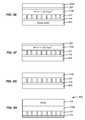
- FIG. 1is a simplified cross-sectional view diagram illustrating a P-type trench gate MOSFET 100 in accordance with an embodiment of the invention. It is to be understood, however, that the principle techniques of the present invention apply to both discrete devices as well as integrated circuits using any processing technology. As with all other figures described herein, it is to be understood that the relative dimensions and sizes of various elements and components depicted in the figures do not exactly reflect actual dimensions and are for illustrative purposes only. As shown, MOSFET 100 includes gate electrodes G that are formed inside trenches 102 . The trenches 102 extend from the top surface of an N ⁇ well body region 104 terminating in a P-type drift or epitaxial region 106 .
- the trenches 102are lined with thin dielectric layers 108 and are substantially covered with conductive material 110 , such as doped polysilicon.
- P-type source regions 112are formed inside the N ⁇ well body region 104 adjacent trenches 102 .
- MOSFET 100includes a N+ body region 117 formed inside the N ⁇ well body region 104 .
- MOSFET 100includes a metal source layer 116 .
- a drain terminal D for MOSFET 100is coupled to a metal substrate 118 disposed on a P-type heavily doped silicon layer 114 .
- the epitaxial layer 106 and body region 104form a semiconductor structure layer 107 disposed on the heavily doped P-type silicon layer 114 .
- FIG. 2is a simplified cross-sectional view diagram illustrating a P-type shielded gate trench MOSFET 200 in accordance with an embodiment of the invention.
- MOSFET 200includes gate electrodes G that are formed inside trenches 202 .
- the trenches 202extend from the top surface of an N ⁇ well body region 204 terminating in a P-type drift or epitaxial region 206 .
- the upper portions of trenches 202are lined with thin gate dielectric layers 208 and are substantially covered with conductive material 210 , such as doped polysilicon, which form the gate electrodes G.
- Shielded gate electrodes 211are insulated from lower portions of the trenches 202 with shield dielectric layers 209 .
- P-type source regions 212are formed inside the N ⁇ well body region 204 adjacent trenches 202 .
- MOSFET 200includes a N+ body region 217 formed inside the N ⁇ well body region 204 .
- MOSFET 200includes a metal source layer 216 .
- a drain terminal D for MOSFET 200is coupled to a metal substrate 218 disposed on a P-type heavily doped silicon layer 214 .
- the epitaxial layer 206 and body region 204form a semiconductor structure layer 207 disposed on the heavily doped P-type silicon layer 214 .
- Rdsonon-resistance
- Q gdgate-to-drain charge
- a methodis provided to fabricate p-channel trench MOSFET device on (110)-oriented silicon wafers with flat (notch) in crystallographic ⁇ 110> direction to reduce the channel resistance. It is known that the hole mobility in the inversion layer can be more than doubled on silicon (110) plane in ⁇ 110> direction ((110)/ ⁇ 110>) than on (100) plane in ⁇ 100> direction ((100)/ ⁇ 100>).
- a relationship between hole mobility and channel resistancecan be expressed in the following equation.
- R chL Z ⁇ ⁇ ⁇ p ⁇ C ox ⁇ ( V G - V T )
- Lis the channel length
- Zis the channel width
- C oxis the gate oxide capacitance per unit area
- V Gis the gate voltage
- ⁇ pis the hole mobility in channel region
- V Tis the threshold voltage.
- the (110)/ ⁇ 110> configurationcan be realized by using (110)-oriented silicon wafers with flat (notch) parallel to the ⁇ 110> crystallographic direction.
- the vertical trenches on this type of wafershave both trench bottom and side wall on (110) planes and the direction of current flow from the trench top to the trench bottom (channel direction) is in the ⁇ 110> direction.
- the present inventionprovides a method for making p-channel trench MOSFET devices on a (110)-oriented silicon substrate with reduced the channel resistance.
- the inventionalso provides a method for reducing drain resistance with heavily doped (110)-oriented silicon substrate.
- a process flow for forming a power device using a heavily doped P-type (110) substrate structureis outlined next.
- An epi layer with a resistivity less than 100 m ⁇ -cm (dopant concentration >1 ⁇ 10 17 cm ⁇ 3 ) and a thickness less than 3.0 ⁇ mis grown on the lightly doped (110) orientation silicon substrate.
- a thermal silicon dioxide layer with a thickness of 400 ⁇ 500 ⁇is grown on the top of the epi layer.
- Hydrogen ions/moleculesare implanted through the silicon dioxide layer at a dose of 3 ⁇ 10 16 cm ⁇ 2 and energy of 60-170 KeV.
- this waferis called the seed wafer hereafter.
- the seed waferis then bonded to another silicon wafer (support substrate) which is topped with a thermal silicon dioxide layer of 1000-2500 ⁇ in thickness, using wafer direct bonding technique performed at room temperature.
- the bonded wafer pairis then subjected to the two-step low temperature annealing procedure.
- the first anneal at 150-300° C. for 10-20 hoursis used for the fusion bond pre-strengthening, and the second anneal at 450° C. for 45 minutes serves for the separation of the heavily boron doped (110)-layer of the seed wafer along the cleaving plane defined by the hydrogen implantation energy.
- the thickness of the transferred heavily boron doped (110)-layeris defined therefore by the energy of the hydrogen implant and range from 0.5 to 1.5 ⁇ m in a specific embodiment.
- FIGS. 4A-4Fare simplified cross-sectional view diagrams illustrating a process flow for forming a heavily doped P-type (110) substrate structure according to an embodiment of the present invention.
- FIG. 4Aillustrates a cross-sectional view of a seed (110) silicon material 402 , which may be doped by dopants such as Boron.
- silicon material 402may be a lightly doped P-type silicon substrate.
- heavily doped layer 404may be formed by implanting dopants in silicon material 402 . Then a thermal silicon oxide layer 406 with a thickness of 400 ⁇ 500 ⁇ is grown on the top of heavily doped layer 404 . Hydrogen ions/molecules are implanted through the silicon dioxide layer at a dose of 3 ⁇ 10 16 cm ⁇ 2 and energy of 60-170 KeV.
- the wafer including layers 402 , 404 , and 406is referred to as the seed wafer 407 hereafter.
- the hydrogen implantcreates a hydrogen rich region 405 delineated as the dotted line in the epi layer 404 .
- An exemplary process for doping hydrogen ions into a silicon substrateis disclosed in U.S. Pat. No. 5,374,564, by Bruel, incorporated herein by reference in its entirety.
- the concentration of hydrogen ionsis provided at a sufficient depth and energy potential to form a hydrogen rich region, or cleavable region, 405 , having an exemplary thickness of between about 1-2 ⁇ m. Because of hydrogen embrittlement, the cleavable region 405 lattice is weaker than non-hydrogen doped silicon lattice.
- FIG. 4Billustrates a cross-sectional view of one embodiment of a first support substrate 308 accordance with embodiments of the invention.
- the first support substrate 308is a (100) silicon substrate.
- the (100) silicon substrateis covered by a silicon dioxide (SiO 2 ) layer 305 .
- the SiO 2 layer 305is used as an etch stop layer and may be virtually any thickness that may be used to advantage.
- the SiO 2 layer 305may be about between 1000 and 2500 ⁇ .
- the SiO 2 layer 305may be about between 2500 and 4000 ⁇ .
- the SiO 2 layer 305may be grown or deposited on the support substrate 308 using virtually any SiO 2 layer formation process.
- the SiO 2 layer 305may be grown using a thermal oxidation process.
- the first support substrate 308 and oxide layer 305is bonded to seed wafer 407 including layers 402 , 404 , and 406 as shown in FIG. 4A .
- oxide layers 305 and 406are bonded together in the bonding process to form oxide layer 306 .
- the bondingcan be carried out using any of a number of bonding techniques. For example, after a wet chemical and de-ionized (DI) water treatment to render the SiO 2 layers 305 and 406 with a hydrophilic surface, the SiO 2 layer 305 and the seed wafer 407 may be bonded at room temperature using conventional bonding techniques.
- DIwet chemical and de-ionized
- a cleaving processis performed to divide the epi layer 404 into two separate layers 114 A and 114 B.
- the cleaving processleaves a lower layer 114 B of heavily doped (110) P-type silicon on the first support substrate 308 and a remaining layer portion 114 A of the epi layer on the seed silicon material 402 .
- the cleavingmay be carried out using any number of cleaving processes to break the lattice structure of the cleavable region 405 .
- the cleaving processincludes annealing the seed wafer 407 and the initial substrate 308 at a temperature of between 150 and 300° C. for about 5 hours to 10 hours.
- the cleaving processincludes annealing the seed wafer 407 and the first support substrate 308 at a temperature of about 450° C. for about 15 minutes.
- the bonded wafer pairis subjected to a two-step low temperature annealing procedure.
- the first anneal at 150-300° C. for 10-20 hoursis used for the fusion bond pre-strengthening, and the second anneal at 450° C. for 45 minutes serves for the separation of the heavily boron doped (110)-layer of the seed wafer along the cleaving plane defined by the hydrogen implantation energy.
- the thickness of the transferred heavily boron doped (110)-layeris defined therefore by energy of the hydrogen implant and range from 0.5 to 1.5 ⁇ m in a specific embodiment.
- FIGS. 4E and 4Fare simplified cross-sectional view diagrams illustrating the two parts formed in the cleaving process described in FIG. 4D .
- a composite material 420is formed which includes lightly doped P-type (110) silicon wafer 402 and a heavily P-type doped (110) epi layer 114 A.
- composite material 420can be used to form another seed wafer, such as seed wafer 407 in FIG. 4A , and used repeatedly in a process as described in FIGS. 4A-4D .
- FIG. 4Fshows a composite material 430 , which includes heavily doped P-type (110) layer 114 B overlying an oxide layer now labeled 306 which overlies the first support substrate 308 .
- layer 114 Bhas a resistivity of 8 m ⁇ -cm, which is much lower than that of commercially available (110) silicon wafers. In one embodiment this layer is used in forming a vertical device and provides a good ohm contact for backside meta layer. An example of a method for forming a vertical device is discussed below.
- FIGS. 5A-5Hare simplified cross-sectional view diagrams illustrating a process flow for forming a vertical device using a heavily doped P-type (110) oriented substrate according to an embodiment of the present invention.
- FIG. 5Aillustrates a cross-sectional view of one embodiment of the semiconductor process structure 430 of FIG. 4F with heavily doped P-type (110) silicon layer 114 B over an oxide layer 306 which in turn overlies support layer 308 .
- support layer 308may be a lightly doped (100) silicon layer.
- layer 114 Bhas a doping concentration of 1E17/cm 3 or higher.
- the structure in FIG. 5Amay be formed using a process described in FIGS. 4A-4F .
- the structure in FIG. 5Amay be formed using another method.
- a lightly doped P-type (110) epitaxial layer 106is formed on the doped P-type (110) silicon layer 114 B.
- the cleaved doped silicon layer 114 Bmay be pretreated in a CVD chamber to prepare the silicon layer 114 B for the epitaxial layer 106 formation. The pretreatment may be used to generate a more uniform surface.
- semiconductor devices 702are formed in and over epitaxial layer 106 and form semiconductor structure layer 107 .
- the formation of the semiconductor structure layer 107may be done by any conventional semiconductor structure formation techniques.
- the semiconductor structures 702may be formed on and/or within the epitaxial layer 106 using conventional semiconductor structure fabrication steps such as layering, patterning, and doping.
- the semiconductor structures 702may also be formed on and/or formed integral to the doped silicon layer 114 B.
- semiconductor structure layer 107may include trench gate MOSFET structures as discussed above in connection with FIG. 1 .
- each semiconductor structures 702is a trench gate MOSFET.
- each semiconductor structures 702is a shielded gate trench MOSFET.
- the metal layer 116is formed on the semiconductor structures 702 .
- the metal layer 116may be applied using virtually any process some of which are described herein.
- the initial substrate 308 , SiO 2 layer 306 , doped silicon layer 114 B, and semiconductor structure layer 107together form another intermediate semiconductor processing structure 507 .
- a second support substrate 802for example, a glass wafer, is mounted to metal layer 116 over the semiconductor structure layer 107 to support the semiconductor process structure 507 for processing.
- second support substrate 802is mounted to the semiconductor process structures 507 using a UV releasable double sided tape, which provides an adhesive bond sufficient in strength to securely hold the intermediate semiconductor process structure for processing.
- the initial support layer 308for example, a (100) silicon substrate, is thinned by a substrate thinning process.
- the initial substrate 308is thinned using a mechanical thinning process such as mechanical polishing/grinding to form a thinner substrate 308 A.
- the initial substrate 308may be thinned, e.g., to about 8 mils to make it faster to remove with chemicals.
- the remaining substrate 308 Ais removed using a substrate etching process.
- the substrate 308 Ais removed by chemically etching the substrate 308 A with a chemical etching process using the buried SiO 2 layer 306 as an etch stop layer.
- the SiO 2 layer 306is configured to stop the chemical etching process, silicon layer 114 B and the semiconductor structure layer 107 remain untouched by the chemical used to etch the initial substrate 308 A.
- the chemical etchingmay be done by any process to remove the initial substrate 308 A.
- the etching processmay be done with chemicals such as acid, hydroxides, and the like, that remove the initial substrate 308 A, but do not etch the buried SiO 2 layer 306 .
- the chemical etching process to remove the initial substrate 308 Amay be illustrated with the following chemical formula: Si+OH ⁇ +2H 2 O ⁇ SiO 2 (OH) 2 ⁇ +H 2 Where SiO 2 (OH) 2 ⁇ is a soluble complex.
- the SiO 2 layer 306is removed by an etching process.
- the buried SiO 2 layer 306may be chemically etched using a solution of HF.
- the heavily doped (110) silicon layer 114 Bis used as the etch stop.
- the SiO 2 layer 306may be etched with a 49 wt % HF solution at room temperature. This particular solution may etch the SiO 2 layer 306 at about 2.5 ⁇ m/min.
- the etching process for removing layer 306can be illustrated with the following chemical equation: SiO 2 +6HF ⁇ H 2 SiF 6 (aq)+2H 2 O
- a metal substrate 118is formed on the doped silicon layer 114 B.
- the metal substrate 118may be formed using virtually any process, such as electroplating and/or using deposition processes such as plasma vapor deposition (PVD), chemical vapor deposition (CVD), and the like.
- the metal substrate 118may be electroplated on the doped silicon layer 114 B.
- the metal substrate 118may include virtually any metal or conductor that may be used to advantage such as copper, aluminum, or alloys such as solder, and the like.
- support layer 802is removed.
- the support layer 802may be removed using any number of techniques.
- the support layer 802may be removed using an ultra violet light process where the bonding tape is configured to release when exposed to a sufficient amount of UV light for a predetermined duration.
- the semiconductor process structure 500 in FIG. 5Hmay be diced into individual devices (dies) in accordance with embodiments of the invention.
- the present inventionprovides a method for fabricating p-channel trench MOSFET device on (110)-oriented silicon material to facilitate hole current conduction in the ⁇ 110> direction to reduce channel resistance.
- the vertical trenches on this type of wafershave both trench bottom and side wall on (110) planes and the direction of current flow from the trench top to the trench bottom (channel direction) is in the ⁇ 110> direction.
- the methodcan be used to form a vertical device, such as trench gate MOSFET or shielded gate trench MOSFET, in which a current conduction in the vertical direction is enhanced. For example, in FIG.
- a currentmay be conducted between metal layers 116 and 118 and through device layer 107 , where device layer 107 may include a trench gate MOSFET or a shielded gate trench MOSFET. In alternative embodiment, device layer 107 may also include other vertical devices such as diodes or IGBTs.
- FIG. 6is a simplified diagram illustrating a relationship between etch rate of a silicon substrate and its boron concentration according to an embodiment of the present invention.
- This diagramis merely an example, which should not unduly limit the scope of the claims herein.
- the etch rate of silicondecreases sharply as its boron concentration is increased above about 1 ⁇ 10 19 cm ⁇ 3 .
- etching rate differencebetween heavily and lightly boron doped silicon substrates with either KOH or ehtylenediamine/pytocatechol/water (EDP).
- the etching rate at boron concentration ⁇ 1 ⁇ 10 19 cm ⁇ 3is about 20 ⁇ m/hr, compared to that of 0.1 ⁇ m/hr at the boron concentration of 1 ⁇ 10 20 cm ⁇ 3 .
- the etching rate differencecan be as large as 200 times.
- a similar etching rate differencehas been observed in KOH chemistry as well. This etching difference will enable the heavily boron doped silicon layer as etching stop.
- This etch selectivity between lightly doped P-type silicon and heavily doped P-type siliconis used advantageously in a method in an embodiment of the present invention.
- FIGS. 7A-7Gare simplified cross-sectional view diagrams illustrating another process flow for forming a vertical device using a heavily doped P-type (110) oriented substrate according to an alternative embodiment of the present invention.
- a heavily boron doped (110) layer 114(with concentration >6 ⁇ 10 19 cm ⁇ 3 ) is epitaxially grown or formed through boron implant on (110) oriented silicon wafer 708 .
- an epi processcan be carried out at 1060° C. with a B 2 H 6 doping species (mixing with H 2 at a concentration of 5000 ppm).
- heavily doped layer 114may be formed by boron ion implantation.
- the implantcan be of 60 KeV with a dose of 1 ⁇ 10 16 cm ⁇ 2 for half an hour to create a heavily doped silicon layer.
- the desired device epi layer 106is grown as shown in FIG. 7B .
- the waferthen undergoes the device fabrication process to build the device.
- device layer 107 and metal layer 116are formed, which may include trench gate MOSFET or shielded gate trench MOSFET, or other vertical devices, such as described in FIGS. 5A-5H .
- the finished waferis then bonded to a support substrate 802 , e.g., a glass carrier as shown in FIG. 7D , and ready for substrate transfer.
- FIG. 7Ethe majority (e.g. 90%) of support substrate silicon wafer 708 is removed through mechanical grinding and acid etching until certain thickness of lightly doped (110) oriented silicon wafer 708 A is left, such as 5 ⁇ m. The final 5 ⁇ m thick silicon 708 A is removed by EDP or KOH. Due to the high selectivity of the EDP/KOH etching, the silicon etching will stop at the heavily doped boron silicon 114 . In FIG. 7F , this wafer is then ready for the backside metal deposition 118 and supporting metal transferring by removing the glass substrate 802 , resulting in the device structure shown in FIG. 7G .
- the methodinclude certain processes, such as vertical device fabrication, support layer bonding, metal deposition, etc, similar to corresponding processes described above in connection with FIGS. 5A-5H .
- FIGS. 7A-7Gare simplified diagrams illustrating an alternative method for forming vertical devices in (110) P-type silicon for enhanced hole mobility which also provides heavily-doped (110) P-type drain regions and metal layers for reducing resistance. As shown, the process is simplified by etch selectivity between heavily doped P-type silicon and lightly doped P-type silicon.
- reducing oxide growth rate and adding additional hydrogen annealingcan further reduce the D it and fixed oxide charge and improve gate oxide integrity.
Landscapes
- Engineering & Computer Science (AREA)
- Microelectronics & Electronic Packaging (AREA)
- Condensed Matter Physics & Semiconductors (AREA)
- General Physics & Mathematics (AREA)
- Manufacturing & Machinery (AREA)
- Computer Hardware Design (AREA)
- Physics & Mathematics (AREA)
- Power Engineering (AREA)
- Chemical & Material Sciences (AREA)
- Chemical Kinetics & Catalysis (AREA)
- General Chemical & Material Sciences (AREA)
- Electrodes Of Semiconductors (AREA)
- Recrystallisation Techniques (AREA)
Abstract
Description
- 1. High mobility p-channel device is realized on the (110)/<110> crystallographically configured silicon wafer to achieve the high hole mobility in the inversion layer;
- 2. The contribution of the lightly doped (110) silicon substrate to device on-resistance is reduced; and
- 3. A (110) oriented silicon-on-metal (SOM) structure allows to substantially improve Rdson without increasing gate charge at the vertical power trench devices.
where L is the channel length, Z is the channel width, Coxis the gate oxide capacitance per unit area, VGis the gate voltage, μpis the hole mobility in channel region, and VTis the threshold voltage. The p-channel devices built on (110)/<110> crystallographically configured wafers thus have much reduced the Rchdue to improved μp.
Si+OH−+2H2O→SiO2(OH)2−+H2
Where SiO2(OH)2− is a soluble complex.
SiO2+6HF→H2SiF6(aq)+2H2O
| TABLE 1 |
| Physical properties of Silicon |
| Surface | |||||
| Density | Available | Ditat mid-gap | |||
| Orientation | 1/cm2 | Bonds 1/cm2 | 1/cm2-eV | ||
| (100) | 6.8 × 10¹⁴ | 6.8 × 10¹⁴ | 2 × 10¹⁰ | ||
| (110) | 9.6 × 10¹⁴ | 9.6 × 10¹⁴ | |||
| (111) | 7.85 × 10¹⁴ | 11.8 × 10¹⁴ | 2 × 10¹¹ | ||
Claims (21)
Priority Applications (1)
| Application Number | Priority Date | Filing Date | Title |
|---|---|---|---|
| US13/328,179US8338886B2 (en) | 2007-09-27 | 2011-12-16 | Semiconductor device with (110)-oriented silicon |
Applications Claiming Priority (3)
| Application Number | Priority Date | Filing Date | Title |
|---|---|---|---|
| US97573907P | 2007-09-27 | 2007-09-27 | |
| US12/174,030US8101500B2 (en) | 2007-09-27 | 2008-07-16 | Semiconductor device with (110)-oriented silicon |
| US13/328,179US8338886B2 (en) | 2007-09-27 | 2011-12-16 | Semiconductor device with (110)-oriented silicon |
Related Parent Applications (1)
| Application Number | Title | Priority Date | Filing Date |
|---|---|---|---|
| US12/174,030DivisionUS8101500B2 (en) | 2007-09-27 | 2008-07-16 | Semiconductor device with (110)-oriented silicon |
Publications (2)
| Publication Number | Publication Date |
|---|---|
| US20120086051A1 US20120086051A1 (en) | 2012-04-12 |
| US8338886B2true US8338886B2 (en) | 2012-12-25 |
Family
ID=40511813
Family Applications (2)
| Application Number | Title | Priority Date | Filing Date |
|---|---|---|---|
| US12/174,030Active2030-11-06US8101500B2 (en) | 2007-09-27 | 2008-07-16 | Semiconductor device with (110)-oriented silicon |
| US13/328,179ActiveUS8338886B2 (en) | 2007-09-27 | 2011-12-16 | Semiconductor device with (110)-oriented silicon |
Family Applications Before (1)
| Application Number | Title | Priority Date | Filing Date |
|---|---|---|---|
| US12/174,030Active2030-11-06US8101500B2 (en) | 2007-09-27 | 2008-07-16 | Semiconductor device with (110)-oriented silicon |
Country Status (5)
| Country | Link |
|---|---|
| US (2) | US8101500B2 (en) |
| KR (1) | KR20100084525A (en) |
| CN (1) | CN101861652B (en) |
| TW (1) | TWI459473B (en) |
| WO (1) | WO2009042547A1 (en) |
Families Citing this family (36)
| Publication number | Priority date | Publication date | Assignee | Title |
|---|---|---|---|---|
| US7635637B2 (en)* | 2005-07-25 | 2009-12-22 | Fairchild Semiconductor Corporation | Semiconductor structures formed on substrates and methods of manufacturing the same |
| JP2008108785A (en)* | 2006-10-23 | 2008-05-08 | Nec Electronics Corp | Semiconductor device and manufacturing method thereof |
| US8564057B1 (en)* | 2007-01-09 | 2013-10-22 | Maxpower Semiconductor, Inc. | Power devices, structures, components, and methods using lateral drift, fixed net charge, and shield |
| KR101287787B1 (en) | 2007-09-12 | 2013-07-18 | 쇼와 덴코 가부시키가이샤 | EPITAXIAL SiC SINGLE CRYSTAL SUBSTRATE AND METHOD FOR MANUFACTURING EPITAXIAL SiC SINGLE CRYSTAL SUBSTRATE |
| US8101500B2 (en) | 2007-09-27 | 2012-01-24 | Fairchild Semiconductor Corporation | Semiconductor device with (110)-oriented silicon |
| US8183628B2 (en)* | 2007-10-29 | 2012-05-22 | Unisantis Electronics Singapore Pte Ltd. | Semiconductor structure and method of fabricating the semiconductor structure |
| JP5317343B2 (en)* | 2009-04-28 | 2013-10-16 | ユニサンティス エレクトロニクス シンガポール プライベート リミテッド | Semiconductor device and manufacturing method thereof |
| US8598650B2 (en)* | 2008-01-29 | 2013-12-03 | Unisantis Electronics Singapore Pte Ltd. | Semiconductor device and production method therefor |
| US20100044827A1 (en)* | 2008-08-22 | 2010-02-25 | Kinik Company | Method for making a substrate structure comprising a film and substrate structure made by same method |
| US8039877B2 (en)* | 2008-09-09 | 2011-10-18 | Fairchild Semiconductor Corporation | (110)-oriented p-channel trench MOSFET having high-K gate dielectric |
| US8278702B2 (en)* | 2008-09-16 | 2012-10-02 | Fairchild Semiconductor Corporation | High density trench field effect transistor |
| JP5356970B2 (en)* | 2009-10-01 | 2013-12-04 | ユニサンティス エレクトロニクス シンガポール プライベート リミテッド | Semiconductor device |
| US8546893B2 (en)* | 2010-01-12 | 2013-10-01 | Mohamed N. Darwish | Devices, components and methods combining trench field plates with immobile electrostatic charge |
| JP4912513B2 (en) | 2010-03-08 | 2012-04-11 | ユニサンティス エレクトロニクス シンガポール プライベート リミテッド | Solid-state imaging device |
| US8487357B2 (en) | 2010-03-12 | 2013-07-16 | Unisantis Electronics Singapore Pte Ltd. | Solid state imaging device having high sensitivity and high pixel density |
| JP5066590B2 (en) | 2010-06-09 | 2012-11-07 | ユニサンティス エレクトロニクス シンガポール プライベート リミテッド | Semiconductor device and manufacturing method thereof |
| JP5087655B2 (en) | 2010-06-15 | 2012-12-05 | ユニサンティス エレクトロニクス シンガポール プライベート リミテッド | Semiconductor device and manufacturing method thereof |
| US20120168819A1 (en)* | 2011-01-03 | 2012-07-05 | Fabio Alessio Marino | Semiconductor pillar power MOS |
| JP2012204395A (en)* | 2011-03-23 | 2012-10-22 | Toshiba Corp | Semiconductor device and manufacturing method of the same |
| US8564034B2 (en) | 2011-09-08 | 2013-10-22 | Unisantis Electronics Singapore Pte. Ltd. | Solid-state imaging device |
| US8669601B2 (en) | 2011-09-15 | 2014-03-11 | Unisantis Electronics Singapore Pte. Ltd. | Method for producing semiconductor device and semiconductor device having pillar-shaped semiconductor |
| US8772175B2 (en) | 2011-12-19 | 2014-07-08 | Unisantis Electronics Singapore Pte. Ltd. | Method for manufacturing semiconductor device and semiconductor device |
| US8916478B2 (en) | 2011-12-19 | 2014-12-23 | Unisantis Electronics Singapore Pte. Ltd. | Method for manufacturing semiconductor device and semiconductor device |
| US8748938B2 (en) | 2012-02-20 | 2014-06-10 | Unisantis Electronics Singapore Pte. Ltd. | Solid-state imaging device |
| ITMI20122226A1 (en)* | 2012-12-21 | 2014-06-22 | St Microelectronics Srl | REALIZATION OF ELECTRONIC DEVICES IN A WAFER IN SEMICONDUCTOR MATERIAL WITH TRINCEE HAVING DIFFERENT DIRECTIONS |
| KR20140142887A (en)* | 2013-06-05 | 2014-12-15 | 에스케이하이닉스 주식회사 | 3 Dimension Semiconductor Device And Method of Manufacturing The same |
| WO2015152904A1 (en)* | 2014-04-01 | 2015-10-08 | Empire Technology Development Llc | Vertical transistor with flashover protection |
| US9406750B2 (en) | 2014-11-19 | 2016-08-02 | Empire Technology Development Llc | Output capacitance reduction in power transistors |
| US9646886B1 (en)* | 2015-12-30 | 2017-05-09 | International Business Machines Corporation | Tailored silicon layers for transistor multi-gate control |
| WO2017189746A1 (en) | 2016-04-27 | 2017-11-02 | Gen-Probe Incorporated | Blood cell lysis reagent |
| US10777670B2 (en)* | 2018-06-25 | 2020-09-15 | Pakal Technologies, Inc. | Vertical insulated gate turn-off thyristor with intermediate p+ layer in p-base formed using epitaxial layer |
| US11295949B2 (en)* | 2019-04-01 | 2022-04-05 | Vishay SIliconix, LLC | Virtual wafer techniques for fabricating semiconductor devices |
| KR102798340B1 (en) | 2019-05-16 | 2025-04-23 | 삼성전자주식회사 | Semiconductor device |
| EP3761357A1 (en)* | 2019-07-04 | 2021-01-06 | Infineon Technologies Austria AG | Semiconductor device |
| FR3110283B1 (en)* | 2020-05-18 | 2022-04-15 | Soitec Silicon On Insulator | Process for manufacturing a semiconductor-on-insulator substrate for radio frequency applications |
| CN116504817B (en)* | 2023-06-29 | 2023-09-19 | 上海陆芯电子科技有限公司 | RC-IGBT structure with fast switching speed and low loss and preparation method thereof |
Citations (43)
| Publication number | Priority date | Publication date | Assignee | Title |
|---|---|---|---|---|
| US4616408A (en) | 1982-11-24 | 1986-10-14 | Hewlett-Packard Company | Inversely processed resistance heater |
| US5344524A (en) | 1993-06-30 | 1994-09-06 | Honeywell Inc. | SOI substrate fabrication |
| US5374564A (en) | 1991-09-18 | 1994-12-20 | Commissariat A L'energie Atomique | Process for the production of thin semiconductor material films |
| US5391257A (en) | 1993-12-10 | 1995-02-21 | Rockwell International Corporation | Method of transferring a thin film to an alternate substrate |
| US5455202A (en) | 1993-01-19 | 1995-10-03 | Hughes Aircraft Company | Method of making a microelectric device using an alternate substrate |
| US5494835A (en) | 1993-12-23 | 1996-02-27 | Commissariat A L'energie Atomique | Process for the production of a relief structure on a semiconductor material support |
| US5528058A (en) | 1986-03-21 | 1996-06-18 | Advanced Power Technology, Inc. | IGBT device with platinum lifetime control and reduced gaw |
| US5714395A (en) | 1995-09-13 | 1998-02-03 | Commissariat A L'energie Atomique | Process for the manufacture of thin films of semiconductor material |
| US5811348A (en) | 1995-02-02 | 1998-09-22 | Sony Corporation | Method for separating a device-forming layer from a base body |
| US5877070A (en) | 1997-05-31 | 1999-03-02 | Max-Planck Society | Method for the transfer of thin layers of monocrystalline material to a desirable substrate |
| US5882987A (en) | 1997-08-26 | 1999-03-16 | International Business Machines Corporation | Smart-cut process for the production of thin semiconductor material films |
| US5998833A (en) | 1998-10-26 | 1999-12-07 | North Carolina State University | Power semiconductor devices having improved high frequency switching and breakdown characteristics |
| US6033489A (en) | 1998-05-29 | 2000-03-07 | Fairchild Semiconductor Corp. | Semiconductor substrate and method of making same |
| US6140210A (en) | 1997-09-26 | 2000-10-31 | Shin-Etsu Handotai Co., Ltd. | Method of fabricating an SOI wafer and SOI wafer fabricated thereby |
| US6372608B1 (en) | 1996-08-27 | 2002-04-16 | Seiko Epson Corporation | Separating method, method for transferring thin film device, thin film device, thin film integrated circuit device, and liquid crystal display device manufactured by using the transferring method |
| US6391744B1 (en) | 1997-03-19 | 2002-05-21 | The United States Of America As Represented By The National Security Agency | Method of fabricating a non-SOI device on an SOI starting wafer and thinning the same |
| US6392290B1 (en) | 2000-04-07 | 2002-05-21 | Siliconix Incorporated | Vertical structure for semiconductor wafer-level chip scale packages |
| US6429481B1 (en) | 1997-11-14 | 2002-08-06 | Fairchild Semiconductor Corporation | Field effect transistor and method of its manufacture |
| US6455398B1 (en) | 1999-07-16 | 2002-09-24 | Massachusetts Institute Of Technology | Silicon on III-V semiconductor bonding for monolithic optoelectronic integration |
| US20020142548A1 (en) | 2001-03-28 | 2002-10-03 | Masaru Takaishi | Semiconductor device and method for manufacturing the same |
| US6468923B1 (en) | 1999-03-26 | 2002-10-22 | Canon Kabushiki Kaisha | Method of producing semiconductor member |
| US6500732B1 (en) | 1999-08-10 | 2002-12-31 | Silicon Genesis Corporation | Cleaving process to fabricate multilayered substrates using low implantation doses |
| US6562647B2 (en) | 1999-09-13 | 2003-05-13 | Vishay Intertechnology, Inc. | Chip scale surface mount package for semiconductor device and process of fabricating the same |
| US20030183876A1 (en) | 2002-03-26 | 2003-10-02 | Yutaka Takafuji | Semiconductor device and manufacturing method thereof, SOI substrate and display device using the same, and manufacturing method of the SOI substrate |
| US6635534B2 (en) | 2000-06-05 | 2003-10-21 | Fairchild Semiconductor Corporation | Method of manufacturing a trench MOSFET using selective growth epitaxy |
| US20040036121A1 (en) | 2002-08-22 | 2004-02-26 | Takaaki Aoki | Semiconductor device and a method of producing the same |
| US6713813B2 (en) | 2001-01-30 | 2004-03-30 | Fairchild Semiconductor Corporation | Field effect transistor having a lateral depletion structure |
| US20040140479A1 (en) | 2003-01-10 | 2004-07-22 | Takeshi Akatsu | Compliant substrate for a heteroepitaxial structure and method for making same |
| US20050017291A1 (en) | 2003-05-30 | 2005-01-27 | Infineon Technologies Ag | Semiconductor structure and method for fabricating such a structure |
| US20050167742A1 (en) | 2001-01-30 | 2005-08-04 | Fairchild Semiconductor Corp. | Power semiconductor devices and methods of manufacture |
| US6939781B2 (en) | 2003-06-27 | 2005-09-06 | Freescale Semiconductor, Inc. | Method of manufacturing a semiconductor component that includes self-aligning a gate electrode to a field plate |
| US20060058210A1 (en) | 2004-09-15 | 2006-03-16 | The Procter & Gamble Company | Wet wipe lotions comprising particulate material |
| US7033891B2 (en) | 2002-10-03 | 2006-04-25 | Fairchild Semiconductor Corporation | Trench gate laterally diffused MOSFET devices and methods for making such devices |
| US20060108635A1 (en)* | 2004-11-23 | 2006-05-25 | Alpha Omega Semiconductor Limited | Trenched MOSFETS with part of the device formed on a (110) crystal plane |
| US7052974B2 (en) | 2001-12-04 | 2006-05-30 | Shin-Etsu Handotai Co., Ltd. | Bonded wafer and method of producing bonded wafer |
| US20060214222A1 (en) | 2003-05-20 | 2006-09-28 | Ashok Challa | Power semiconductor devices and methods of manufacture |
| US20060273386A1 (en) | 2005-05-26 | 2006-12-07 | Hamza Yilmaz | Trench-gate field effect transistors and methods of forming the same |
| US20070020884A1 (en)* | 2005-07-25 | 2007-01-25 | Qi Wang | Semiconductor structures formed on substrates and methods of manufacturing the same |
| US20070032020A1 (en) | 2005-06-29 | 2007-02-08 | Grebs Thomas E | Structures and methods for forming shielded gate field effect transistors |
| US20070190728A1 (en) | 2006-02-10 | 2007-08-16 | Sreevatsa Sreekantham | Low resistance gate for power mosfet applications and method of manufacture |
| US20070262360A1 (en) | 2005-12-22 | 2007-11-15 | Deva Pattanayak | High mobility power metal-oxide semiconductor field-effect transistors |
| US20080261379A1 (en) | 2007-04-20 | 2008-10-23 | Semiconductor Energy Laboratory Co., Ltd. | Method for manufacturing SOI substrate and semiconductor device |
| US8039877B2 (en) | 2008-09-09 | 2011-10-18 | Fairchild Semiconductor Corporation | (110)-oriented p-channel trench MOSFET having high-K gate dielectric |
Family Cites Families (2)
| Publication number | Priority date | Publication date | Assignee | Title |
|---|---|---|---|---|
| US7078722B2 (en)* | 2004-09-20 | 2006-07-18 | International Business Machines Corporation | NFET and PFET devices and methods of fabricating same |
| US8101500B2 (en) | 2007-09-27 | 2012-01-24 | Fairchild Semiconductor Corporation | Semiconductor device with (110)-oriented silicon |
- 2008
- 2008-07-16USUS12/174,030patent/US8101500B2/enactiveActive
- 2008-09-22WOPCT/US2008/077240patent/WO2009042547A1/enactiveApplication Filing
- 2008-09-22KRKR1020107009063Apatent/KR20100084525A/ennot_activeCeased
- 2008-09-22CNCN2008801094901Apatent/CN101861652B/ennot_activeExpired - Fee Related
- 2008-09-26TWTW097137173Apatent/TWI459473B/enactive
- 2011
- 2011-12-16USUS13/328,179patent/US8338886B2/enactiveActive
Patent Citations (46)
| Publication number | Priority date | Publication date | Assignee | Title |
|---|---|---|---|---|
| US4616408A (en) | 1982-11-24 | 1986-10-14 | Hewlett-Packard Company | Inversely processed resistance heater |
| US5528058A (en) | 1986-03-21 | 1996-06-18 | Advanced Power Technology, Inc. | IGBT device with platinum lifetime control and reduced gaw |
| US5374564A (en) | 1991-09-18 | 1994-12-20 | Commissariat A L'energie Atomique | Process for the production of thin semiconductor material films |
| US5455202A (en) | 1993-01-19 | 1995-10-03 | Hughes Aircraft Company | Method of making a microelectric device using an alternate substrate |
| US5344524A (en) | 1993-06-30 | 1994-09-06 | Honeywell Inc. | SOI substrate fabrication |
| US5391257A (en) | 1993-12-10 | 1995-02-21 | Rockwell International Corporation | Method of transferring a thin film to an alternate substrate |
| US5494835A (en) | 1993-12-23 | 1996-02-27 | Commissariat A L'energie Atomique | Process for the production of a relief structure on a semiconductor material support |
| US5811348A (en) | 1995-02-02 | 1998-09-22 | Sony Corporation | Method for separating a device-forming layer from a base body |
| US5714395A (en) | 1995-09-13 | 1998-02-03 | Commissariat A L'energie Atomique | Process for the manufacture of thin films of semiconductor material |
| US6372608B1 (en) | 1996-08-27 | 2002-04-16 | Seiko Epson Corporation | Separating method, method for transferring thin film device, thin film device, thin film integrated circuit device, and liquid crystal display device manufactured by using the transferring method |
| US6391744B1 (en) | 1997-03-19 | 2002-05-21 | The United States Of America As Represented By The National Security Agency | Method of fabricating a non-SOI device on an SOI starting wafer and thinning the same |
| US5877070A (en) | 1997-05-31 | 1999-03-02 | Max-Planck Society | Method for the transfer of thin layers of monocrystalline material to a desirable substrate |
| US5882987A (en) | 1997-08-26 | 1999-03-16 | International Business Machines Corporation | Smart-cut process for the production of thin semiconductor material films |
| US6140210A (en) | 1997-09-26 | 2000-10-31 | Shin-Etsu Handotai Co., Ltd. | Method of fabricating an SOI wafer and SOI wafer fabricated thereby |
| US6828195B2 (en) | 1997-11-14 | 2004-12-07 | Fairchild Semiconductor Corporation | Method of manufacturing a trench transistor having a heavy body region |
| US6429481B1 (en) | 1997-11-14 | 2002-08-06 | Fairchild Semiconductor Corporation | Field effect transistor and method of its manufacture |
| US6033489A (en) | 1998-05-29 | 2000-03-07 | Fairchild Semiconductor Corp. | Semiconductor substrate and method of making same |
| US5998833A (en) | 1998-10-26 | 1999-12-07 | North Carolina State University | Power semiconductor devices having improved high frequency switching and breakdown characteristics |
| US6468923B1 (en) | 1999-03-26 | 2002-10-22 | Canon Kabushiki Kaisha | Method of producing semiconductor member |
| US6455398B1 (en) | 1999-07-16 | 2002-09-24 | Massachusetts Institute Of Technology | Silicon on III-V semiconductor bonding for monolithic optoelectronic integration |
| US6500732B1 (en) | 1999-08-10 | 2002-12-31 | Silicon Genesis Corporation | Cleaving process to fabricate multilayered substrates using low implantation doses |
| US6562647B2 (en) | 1999-09-13 | 2003-05-13 | Vishay Intertechnology, Inc. | Chip scale surface mount package for semiconductor device and process of fabricating the same |
| US6392290B1 (en) | 2000-04-07 | 2002-05-21 | Siliconix Incorporated | Vertical structure for semiconductor wafer-level chip scale packages |
| US6635534B2 (en) | 2000-06-05 | 2003-10-21 | Fairchild Semiconductor Corporation | Method of manufacturing a trench MOSFET using selective growth epitaxy |
| US20050167742A1 (en) | 2001-01-30 | 2005-08-04 | Fairchild Semiconductor Corp. | Power semiconductor devices and methods of manufacture |
| US6713813B2 (en) | 2001-01-30 | 2004-03-30 | Fairchild Semiconductor Corporation | Field effect transistor having a lateral depletion structure |
| US20020142548A1 (en) | 2001-03-28 | 2002-10-03 | Masaru Takaishi | Semiconductor device and method for manufacturing the same |
| US7052974B2 (en) | 2001-12-04 | 2006-05-30 | Shin-Etsu Handotai Co., Ltd. | Bonded wafer and method of producing bonded wafer |
| US20030183876A1 (en) | 2002-03-26 | 2003-10-02 | Yutaka Takafuji | Semiconductor device and manufacturing method thereof, SOI substrate and display device using the same, and manufacturing method of the SOI substrate |
| US20040036121A1 (en) | 2002-08-22 | 2004-02-26 | Takaaki Aoki | Semiconductor device and a method of producing the same |
| US7033891B2 (en) | 2002-10-03 | 2006-04-25 | Fairchild Semiconductor Corporation | Trench gate laterally diffused MOSFET devices and methods for making such devices |
| US20040140479A1 (en) | 2003-01-10 | 2004-07-22 | Takeshi Akatsu | Compliant substrate for a heteroepitaxial structure and method for making same |
| US20060214222A1 (en) | 2003-05-20 | 2006-09-28 | Ashok Challa | Power semiconductor devices and methods of manufacture |
| US20050017291A1 (en) | 2003-05-30 | 2005-01-27 | Infineon Technologies Ag | Semiconductor structure and method for fabricating such a structure |
| US6939781B2 (en) | 2003-06-27 | 2005-09-06 | Freescale Semiconductor, Inc. | Method of manufacturing a semiconductor component that includes self-aligning a gate electrode to a field plate |
| US20060058210A1 (en) | 2004-09-15 | 2006-03-16 | The Procter & Gamble Company | Wet wipe lotions comprising particulate material |
| US20060108635A1 (en)* | 2004-11-23 | 2006-05-25 | Alpha Omega Semiconductor Limited | Trenched MOSFETS with part of the device formed on a (110) crystal plane |
| US20060273386A1 (en) | 2005-05-26 | 2006-12-07 | Hamza Yilmaz | Trench-gate field effect transistors and methods of forming the same |
| US20070032020A1 (en) | 2005-06-29 | 2007-02-08 | Grebs Thomas E | Structures and methods for forming shielded gate field effect transistors |
| US20070020884A1 (en)* | 2005-07-25 | 2007-01-25 | Qi Wang | Semiconductor structures formed on substrates and methods of manufacturing the same |
| US7635637B2 (en) | 2005-07-25 | 2009-12-22 | Fairchild Semiconductor Corporation | Semiconductor structures formed on substrates and methods of manufacturing the same |
| US20100052046A1 (en) | 2005-07-25 | 2010-03-04 | Fairchild Semiconductor Corporation | Semiconductor structures formed on substrates and methods of manufacturing the same |
| US20070262360A1 (en) | 2005-12-22 | 2007-11-15 | Deva Pattanayak | High mobility power metal-oxide semiconductor field-effect transistors |
| US20070190728A1 (en) | 2006-02-10 | 2007-08-16 | Sreevatsa Sreekantham | Low resistance gate for power mosfet applications and method of manufacture |
| US20080261379A1 (en) | 2007-04-20 | 2008-10-23 | Semiconductor Energy Laboratory Co., Ltd. | Method for manufacturing SOI substrate and semiconductor device |
| US8039877B2 (en) | 2008-09-09 | 2011-10-18 | Fairchild Semiconductor Corporation | (110)-oriented p-channel trench MOSFET having high-K gate dielectric |
Non-Patent Citations (7)
| Title |
|---|
| Bruel, M., "Silicon on Insulator Material Technology", Electronics Letters, Jul. 6, 1995, vol. 31, No. 14, pp. 1201-1202. |
| Celler, C.K. et al., "Frontiers of silicon-on-insulator", Journal of Applied Physics, vol. 93, No. 9, pp. 4955-4978. |
| Green, M. L., "Nucleation and growth of atomic layer deposited HfO2 gate dielectric layers on chemical oxide (Si-O-H) and thermal oxide (SiO2 or Si-O-N) underlayers", Journal of Applied Physics, vol. 92, No. 12, Dec. 12, 2002, pp. 7168-7174. |
| Irie et al., "In-Plane Mobility Anisotrophy and Universality Undeer Uni-axial Strains in n- and p-MOS Inversion Layers on (100), (110), and (111) Si," IEEE pp. 9.5.1 to 9.5.4 (2004). |
| Sze, S.M., eds. Physics of Semiconductor Devices, 2nd Edition, pp. 380-390, John Wiley and Sons, New York, 1981. |
| Tong, Q.Y. et al., "Layer splitting process in hydrogen-implanted Si, Ge, SiC, and diamond substrates", Mar. 17, 1997, Appl. Phys. Lett., vol. 70, No. 11, pp. 1390-1392. |
| Tong, Q.Y. et al., "Layer Transfer by Bonding and Layer Splitting", 1999, Semiconductor Wafer Bonding: Science and Technology, John Wiley & Sons, Inc., pp. 161-165. |
Also Published As
| Publication number | Publication date |
|---|---|
| TWI459473B (en) | 2014-11-01 |
| US8101500B2 (en) | 2012-01-24 |
| US20120086051A1 (en) | 2012-04-12 |
| KR20100084525A (en) | 2010-07-26 |
| CN101861652A (en) | 2010-10-13 |
| US20090179259A1 (en) | 2009-07-16 |
| CN101861652B (en) | 2013-06-12 |
| TW200924077A (en) | 2009-06-01 |
| WO2009042547A1 (en) | 2009-04-02 |
Similar Documents
| Publication | Publication Date | Title |
|---|---|---|
| US8338886B2 (en) | Semiconductor device with (110)-oriented silicon | |
| US8039877B2 (en) | (110)-oriented p-channel trench MOSFET having high-K gate dielectric | |
| US11495489B2 (en) | Method for forming a semiconductor-on-insulator (SOI) substrate | |
| US9117836B2 (en) | Silicon carbide semiconductor device and manufacturing method thereof | |
| US20100052046A1 (en) | Semiconductor structures formed on substrates and methods of manufacturing the same | |
| CN101584029B (en) | Process for manufacturing semiconductor device | |
| US10410911B2 (en) | Buried insulator regions and methods of formation thereof | |
| TW201137985A (en) | Multi-gate semiconductor device with self-aligned epitaxial source and drain | |
| WO2012009927A1 (en) | Process for producing soi super junction ldmos structure completely eliminating effect of substrate assisted depletion | |
| US9570441B2 (en) | Semiconductor device with thermally grown oxide layer between field and gate electrode and method of manufacturing | |
| US9570613B2 (en) | Structure and formation method of FinFET device | |
| JP2001127289A (en) | Semiconductor device and method of manufacturing semiconductor device | |
| TW200903806A (en) | Power MOSFET structure and manufacturing method for the same | |
| US10121859B2 (en) | Method of manufacturing semiconductor devices with transistor cells and semiconductor device | |
| US6858499B2 (en) | Method for fabrication of MOSFET with buried gate | |
| US8039401B2 (en) | Structure and method for forming hybrid substrate | |
| KR101336219B1 (en) | Fully Depleted SOI Device with Buried Doping Layer | |
| US20250280576A1 (en) | Semiconductor component and method for production | |
| CN116344574A (en) | Ultra-thin silicon-on-insulator device and method of forming the same | |
| JP2000223721A (en) | High breakdown voltage semiconductor device and method of manufacturing the same |
Legal Events
| Date | Code | Title | Description |
|---|---|---|---|
| STCF | Information on status: patent grant | Free format text:PATENTED CASE | |
| FPAY | Fee payment | Year of fee payment:4 | |
| AS | Assignment | Owner name:DEUTSCHE BANK AG NEW YORK BRANCH, AS COLLATERAL AGENT, NEW YORK Free format text:PATENT SECURITY AGREEMENT;ASSIGNOR:FAIRCHILD SEMICONDUCTOR CORPORATION;REEL/FRAME:040075/0644 Effective date:20160916 Owner name:DEUTSCHE BANK AG NEW YORK BRANCH, AS COLLATERAL AG Free format text:PATENT SECURITY AGREEMENT;ASSIGNOR:FAIRCHILD SEMICONDUCTOR CORPORATION;REEL/FRAME:040075/0644 Effective date:20160916 | |
| MAFP | Maintenance fee payment | Free format text:PAYMENT OF MAINTENANCE FEE, 8TH YEAR, LARGE ENTITY (ORIGINAL EVENT CODE: M1552); ENTITY STATUS OF PATENT OWNER: LARGE ENTITY Year of fee payment:8 | |
| AS | Assignment | Owner name:SEMICONDUCTOR COMPONENTS INDUSTRIES, LLC, ARIZONA Free format text:ASSIGNMENT OF ASSIGNORS INTEREST;ASSIGNOR:FAIRCHILD SEMICONDUCTOR CORPORATION;REEL/FRAME:057694/0374 Effective date:20210722 | |
| AS | Assignment | Owner name:FAIRCHILD SEMICONDUCTOR CORPORATION, ARIZONA Free format text:RELEASE BY SECURED PARTY;ASSIGNOR:DEUTSCHE BANK AG NEW YORK BRANCH;REEL/FRAME:057969/0206 Effective date:20211027 | |
| AS | Assignment | Owner name:DEUTSCHE BANK AG NEW YORK BRANCH, AS COLLATERAL AGENT, NEW YORK Free format text:SECURITY INTEREST;ASSIGNOR:SEMICONDUCTOR COMPONENTS INDUSTRIES, LLC;REEL/FRAME:058871/0799 Effective date:20211028 | |
| AS | Assignment | Owner name:FAIRCHILD SEMICONDUCTOR CORPORATION, ARIZONA Free format text:RELEASE OF SECURITY INTEREST IN PATENTS RECORDED AT REEL 040075, FRAME 0644;ASSIGNOR:DEUTSCHE BANK AG NEW YORK BRANCH, AS COLLATERAL AGENT;REEL/FRAME:064070/0536 Effective date:20230622 Owner name:SEMICONDUCTOR COMPONENTS INDUSTRIES, LLC, ARIZONA Free format text:RELEASE OF SECURITY INTEREST IN PATENTS RECORDED AT REEL 040075, FRAME 0644;ASSIGNOR:DEUTSCHE BANK AG NEW YORK BRANCH, AS COLLATERAL AGENT;REEL/FRAME:064070/0536 Effective date:20230622 | |
| AS | Assignment | Owner name:FAIRCHILD SEMICONDUCTOR CORPORATION, ARIZONA Free format text:RELEASE OF SECURITY INTEREST IN PATENTS RECORDED AT REEL 058871, FRAME 0799;ASSIGNOR:DEUTSCHE BANK AG NEW YORK BRANCH, AS COLLATERAL AGENT;REEL/FRAME:065653/0001 Effective date:20230622 Owner name:SEMICONDUCTOR COMPONENTS INDUSTRIES, LLC, ARIZONA Free format text:RELEASE OF SECURITY INTEREST IN PATENTS RECORDED AT REEL 058871, FRAME 0799;ASSIGNOR:DEUTSCHE BANK AG NEW YORK BRANCH, AS COLLATERAL AGENT;REEL/FRAME:065653/0001 Effective date:20230622 | |
| MAFP | Maintenance fee payment | Free format text:PAYMENT OF MAINTENANCE FEE, 12TH YEAR, LARGE ENTITY (ORIGINAL EVENT CODE: M1553); ENTITY STATUS OF PATENT OWNER: LARGE ENTITY Year of fee payment:12 |