US8338809B2 - Ultraviolet reflector with coolant gas holes and method - Google Patents
Ultraviolet reflector with coolant gas holes and methodDownload PDFInfo
- Publication number
- US8338809B2 US8338809B2US13/164,745US201113164745AUS8338809B2US 8338809 B2US8338809 B2US 8338809B2US 201113164745 AUS201113164745 AUS 201113164745AUS 8338809 B2US8338809 B2US 8338809B2
- Authority
- US
- United States
- Prior art keywords
- reflector
- ultraviolet lamp
- ultraviolet
- lamp
- dichroic coating
- Prior art date
- Legal status (The legal status is an assumption and is not a legal conclusion. Google has not performed a legal analysis and makes no representation as to the accuracy of the status listed.)
- Active
Links
Images


Classifications
- H—ELECTRICITY
- H01—ELECTRIC ELEMENTS
- H01L—SEMICONDUCTOR DEVICES NOT COVERED BY CLASS H10
- H01L21/00—Processes or apparatus adapted for the manufacture or treatment of semiconductor or solid state devices or of parts thereof
- H01L21/67—Apparatus specially adapted for handling semiconductor or electric solid state devices during manufacture or treatment thereof; Apparatus specially adapted for handling wafers during manufacture or treatment of semiconductor or electric solid state devices or components ; Apparatus not specifically provided for elsewhere
- H01L21/67005—Apparatus not specifically provided for elsewhere
- H01L21/67011—Apparatus for manufacture or treatment
- H01L21/67098—Apparatus for thermal treatment
- H01L21/67115—Apparatus for thermal treatment mainly by radiation
- G—PHYSICS
- G21—NUCLEAR PHYSICS; NUCLEAR ENGINEERING
- G21K—TECHNIQUES FOR HANDLING PARTICLES OR IONISING RADIATION NOT OTHERWISE PROVIDED FOR; IRRADIATION DEVICES; GAMMA RAY OR X-RAY MICROSCOPES
- G21K1/00—Arrangements for handling particles or ionising radiation, e.g. focusing or moderating
- G21K1/06—Arrangements for handling particles or ionising radiation, e.g. focusing or moderating using diffraction, refraction or reflection, e.g. monochromators
- G21K1/062—Devices having a multilayer structure
- B—PERFORMING OPERATIONS; TRANSPORTING
- B82—NANOTECHNOLOGY
- B82Y—SPECIFIC USES OR APPLICATIONS OF NANOSTRUCTURES; MEASUREMENT OR ANALYSIS OF NANOSTRUCTURES; MANUFACTURE OR TREATMENT OF NANOSTRUCTURES
- B82Y10/00—Nanotechnology for information processing, storage or transmission, e.g. quantum computing or single electron logic
- H—ELECTRICITY
- H01—ELECTRIC ELEMENTS
- H01L—SEMICONDUCTOR DEVICES NOT COVERED BY CLASS H10
- H01L21/00—Processes or apparatus adapted for the manufacture or treatment of semiconductor or solid state devices or of parts thereof
- H01L21/67—Apparatus specially adapted for handling semiconductor or electric solid state devices during manufacture or treatment thereof; Apparatus specially adapted for handling wafers during manufacture or treatment of semiconductor or electric solid state devices or components ; Apparatus not specifically provided for elsewhere
- H01L21/67005—Apparatus not specifically provided for elsewhere
- H01L21/67011—Apparatus for manufacture or treatment
- H01L21/67017—Apparatus for fluid treatment
- H01L21/67028—Apparatus for fluid treatment for cleaning followed by drying, rinsing, stripping, blasting or the like
- H01L21/67034—Apparatus for fluid treatment for cleaning followed by drying, rinsing, stripping, blasting or the like for drying
- G—PHYSICS
- G21—NUCLEAR PHYSICS; NUCLEAR ENGINEERING
- G21K—TECHNIQUES FOR HANDLING PARTICLES OR IONISING RADIATION NOT OTHERWISE PROVIDED FOR; IRRADIATION DEVICES; GAMMA RAY OR X-RAY MICROSCOPES
- G21K2201/00—Arrangements for handling radiation or particles
- G21K2201/06—Arrangements for handling radiation or particles using diffractive, refractive or reflecting elements
- G21K2201/064—Arrangements for handling radiation or particles using diffractive, refractive or reflecting elements having a curved surface
- G—PHYSICS
- G21—NUCLEAR PHYSICS; NUCLEAR ENGINEERING
- G21K—TECHNIQUES FOR HANDLING PARTICLES OR IONISING RADIATION NOT OTHERWISE PROVIDED FOR; IRRADIATION DEVICES; GAMMA RAY OR X-RAY MICROSCOPES
- G21K2201/00—Arrangements for handling radiation or particles
- G21K2201/06—Arrangements for handling radiation or particles using diffractive, refractive or reflecting elements
- G21K2201/065—Arrangements for handling radiation or particles using diffractive, refractive or reflecting elements provided with cooling means
- G—PHYSICS
- G21—NUCLEAR PHYSICS; NUCLEAR ENGINEERING
- G21K—TECHNIQUES FOR HANDLING PARTICLES OR IONISING RADIATION NOT OTHERWISE PROVIDED FOR; IRRADIATION DEVICES; GAMMA RAY OR X-RAY MICROSCOPES
- G21K2201/00—Arrangements for handling radiation or particles
- G21K2201/06—Arrangements for handling radiation or particles using diffractive, refractive or reflecting elements
- G21K2201/067—Construction details
Definitions
- Embodiments of the present apparatus and methodrelate generally to the ultraviolet treatment of a substrate.
- layers of dielectric, semiconducting, and conducting materialsare formed on a substrate such as a semiconductor wafer, glass panel or metal panel. These layers are then processed to form features such as electrical interconnects, dielectric layers, gates and electrodes.
- ultraviolet radiationcan be used to treat the layers or features formed on the substrate.
- ultraviolet radiationcan be used in rapid thermal processing (RTP) to rapidly heat a layer formed on the substrate.
- RTPrapid thermal processing
- Ultraviolet radiationis also used to promote condensation and polymerization of polymeric layers.
- Ultraviolet radiationcan also be used to generate stressed film layers. Ultraviolet radiation can also be used to activate gases to clean a chamber.
- UV radiationis used to treat films of silicon oxide, silicon carbide, or carbon-doped silicon oxide.
- materialssuch as silicon oxide (SiO x ), silicon carbide (SiC), and silicon-oxygen-carbon (SiOC x ) films are used as dielectric layers in the fabrication of semiconductor devices.
- Chemical vapor deposition (CVD) methodsare often used to deposit these films, and involve promoting a thermal or plasma based reaction between a silicon supplying source and an oxygen supplying source in a CVD chamber.
- watercan be formed as a by-product of the CVD or other reaction.
- watercan be formed in the deposition of silicon-oxygen-carbon or silicon carbide films by CVD processes that use an organosilane source which includes at least one Si—C bond.
- the process-generated watercan be physically absorbed into the films as moisture or incorporated into the deposited film as Si—OH chemical bond, both of which are undesirable.
- Ultraviolet radiationcan be used to treat these films to cure and densify the deposited CVD film.
- ultraviolet treatmentreduces the overall thermal budget of an individual wafer and speeds up the fabrication process.
- a number of ultraviolet curing chambershave been developed which can be used to effectively cure films deposited on substrates 38 , such as, for example, U.S. application Ser. No.: 11/124,908, filed May 9, 2005, and published as Patent Application Publication No. U.S. 2006/0251827 A1 entitled “Tandem UV Chamber for Curing Dielectric Materials” which is assigned to Applied Materials, Inc., of Santa Clara, Calif. and incorporated by reference herein and in its entirety.
- a reflector for an ultraviolet lampcan be used in a substrate processing apparatus.
- the reflectorcomprises a centrally positioned longitudinal strip and first and second side reflectors.
- the longitudinal striphas a plurality of through holes therein to direct a coolant gas toward the ultraviolet lamp and a curved reflective surface with a dichroic coating.
- the first and second side reflectorsare positioned on either side of the centrally positioned reflector to form a parabolic-type surface with the centrally positioned reflector.
- the first and second side reflectorseach have an arcuate reflective surface with the dichroic coating.
- a substrate process chambercomprises a substrate support and ultraviolet lamp module comprising (i) an elongated ultraviolet lamp spaced apart from the substrate support, the ultraviolet lamp configured to transmit ultraviolet light toward the substrate support; and (ii) a primary reflector comprising: (1) a centrally positioned reflector comprising a longitudinal strip having a plurality of through holes therein and a curved reflective surface with a dichroic coating; and (2) first and second side reflectors that are positioned on either side of the centrally positioned reflector to form a parabolic-type surface with the centrally positioned reflector, the first and second side reflectors each having an arcuate reflective surface with the dichroic coating.
- a method of treating a substrate with ultraviolet radiationcomprises providing a substrate in a process zone.
- An ultraviolet lampis energized to generate ultraviolet radiation.
- a primary reflectoris supported behind the ultraviolet lamp and comprises (i) a centrally positioned reflector comprising a longitudinal strip having a plurality of through holes therein to direct a coolant gas toward the ultraviolet lamp, and a curved reflective surface with a dichroic coating; and (ii) first and second side reflectors that are positioned on either side of the centrally positioned reflector to form a parabolic-type surface with the centrally positioned reflector, the first and second side reflectors each having an arcuate reflective surface with the dichroic coating.
- a plurality of streams of coolant gasare directed through holes in the curved reflective surface to cool the ultraviolet lamp.
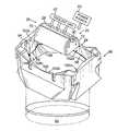
- FIG. 1is a schematic perspective view of an embodiment of an ultraviolet (UV) lamp module comprising a UV lamp and a primary reflector positioned above a quartz window and a substrate;
- UVultraviolet
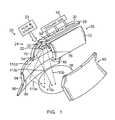
- FIG. 2is a top perspective view of the UV lamp module and a reflector assembly comprising primary and secondary reflectors;
- FIG. 3Ais a perspective view of a central reflector looking up at the curved reflective surface of the reflector, showing a portion of the reflector holder, and the coolant gas flow through the holes of the central reflector and over the UV lamp;
- FIG. 3Bis a side view of the central reflector taken along viewing line 3 B in FIG. 3A , showing the gas flow through the holes and around the UV lamp;
- FIGS. 4A and 4Bare computer modeled diagrams of the coolant gas in a conventional system ( FIG. 4A ) and through the holes of a central reflector and around a UV lamp ( FIG. 4B );
- FIG. 5is a schematic cross-sectional view of a tandem chamber according to an embodiment of the present invention.
- FIG. 6is a schematic top plan view of a substrate processing apparatus according to an embodiment of the present invention.
- UV lamp module 20that can generate ultraviolet radiation to treat substrates 38 such as semiconducting wafers, displays, and solar panels, is shown in FIG. 1 .
- the UV lamp module 20comprises a UV lamp 22 that emits ultraviolet radiation.
- the UV lamp 22can include any UV source such as a mercury microwave arc lamp, pulsed xenon flash lamp, or high-efficiency UV light emitting diode array.
- the UV lamp 22is a sealed plasma bulb filled with a gas such as xenon (Xe) or mercury (Hg), and which is excited by an external power source 23 such as a microwave generator that includes a magnetron and a transformer to energize filaments of the magnetron.
- Xexenon
- Hgmercury
- the UV lamp 22can include a filament which is powered by a power source 23 (shown schematically) that supplies direct current to the filament.
- the UV lamp 22can also be powered by a power source 23 comprising a radio frequency (RF) energy source that can excite the gas within the UV lamp 22 .
- RFradio frequency
- the UV lamp 22is shown as an elongated cylindrical bulb for illustrative purposes; however, UV lamps 22 having other shapes can also be used, such as spherical lamps or arrays of lamps, as would be apparent to one of ordinary skill in the art.
- a suitable UV lamp 22is commercially available from, for example, Nordson Corporation in Westlake, Ohio; or from Miltec UV Company in Stevenson, Md.
- the UV lamp 22includes a single elongated UV H+ bulb from Miltec UV Company.
- the UV lamp 22may include two or more separate elongated bulbs.
- the lamp module 20includes a reflector assembly 24 that includes a primary reflector 26 that partially surrounds the UV lamp 22 of the ultraviolet lamp module 20 .
- the primary reflector 26comprises a central reflector 28 that is centrally positioned behind, and in a spaced relationship with respect to, the UV lamp 22 .
- the central reflector 28comprises a longitudinal strip 30 that extends the length of the ultraviolet lamp, as shown in FIGS. 3A and 3B .
- the longitudinal strip 30has a curved reflective surface 32 that is an interior surface and which faces the back of the UV lamp 22 to reflect backward directed rays of ultraviolet radiation emitted by the UV lamp 22 towards the substrate 38 .
- the curved reflective surface 32 of the longitudinal strip 30is an arcuate surface that can be circular, elliptical, or parabolic.
- the curved reflective surface 32comprises a circular surface with a radius of curvature of at least about 2 cm and less than about 5 cm or even from about 3 to about 4 cm.
- the longitudinal strip 30also has a back surface 34 , which can be flat, or can be curved to match the curvature of the curved reflective surface 32 .
- the longitudinal strip 30is made from a material that allows transmission of infrared radiation and microwaves, and which reflects ultraviolet radiation.
- the longitudinal strip 30comprises quartz.
- an elongated preform of quartzcan be machined to form the longitudinal strip 30 .
- Conventional machining techniques, such as CNC,can be used to machine a cast quartz preform to obtain the desired shape of the longitudinal strip 30 including the curved reflective surface 32 on the front of the strip 30 .
- the curved reflective surface 32is formed by polishing the interior facing surface using conventional polishing methods so that at least 95% of the surface 32 is free of wrinkles and cracks.
- a dichroic coating 36can also be applied to the curved reflective surface 32 of the longitudinal strip 30 to reflect a higher percentage of the backward directed ultraviolet rays toward the substrate 38 .
- the dichroic coating 36is a thin-film filter that selectively passes through light having a small range of wavelengths while reflecting other wavelengths.
- the dichroic coating 36comprises a multilayer film composed of different dielectric materials.
- the different dielectric materialscan include a plurality of layers having alternating high and low refractive indices, and which are arranged and selected so that the dichroic coating 36 does not reflect all of the damaging heat-generating infrared radiation emitted by the UV lamp 22 , but instead allows some of this radiation to pass into the longitudinal strip 30 .
- the quartz material of the strip 30transmits infrared light and the dichroic coating 36 reflects ultraviolet light emitted by the UV lamp 22 . Since the dichroic coating is non-metallic, microwave radiation applied to the UV lamp 22 from a power source (not shown) that is downwardly incident on the backside of the quartz does not significantly interact with, or get absorbed by, the modulated layers and is readily transmitted for ionizing the gas in the UV lamp 22 .
- a secondary reflective coatingmay also be applied to the back surface 34 to reflect back any ultraviolet radiation that passes through the curved reflective surface 32 at the front of the longitudinal strip 30 , or to more rapidly dissipate heat accumulated in the longitudinal strip 30 from exposure to the ultraviolet radiation.
- a plurality of through holes 40are provided in the longitudinal strip 30 .
- the holes 40extend from the back surface 34 to the curved reflective surface 32 to allow a coolant gas 42 to be injected from an external coolant gas source toward the UV lamp 22 .
- the holes 40include first holes 44 having a first diameter that is larger than a second diameter of the second holes 46 .
- the first and second holes 44 , 46are lined along a central axis 48 of the longitudinal strip 30 .
- the first holes 44can have a diameter of from about 0.2 mm to about 4 mm
- the second holes 46can have a diameter of from about 6 mm to about 12 mm.
- the total number of first holes 44can range from about 10 to about 50, and the total number of second holes 46 can range from about 2 to about 6.
- the edges of the holes 44 , 46can be angled or sloped to cause the coolant gas 42 to be injected toward the UV lamp 22 .
- a suitable anglecan range from about 10° to about 45°, such as 25°.
- each end 50 a,b of the longitudinal strip 30 of the central reflector 28comprises an end tab 52 a,b .
- a reflector holder 54comprises end holders 56 a,b that each have a cutout 58 a,b that is shaped so that each end tab 52 a,b of the central reflector 28 fits into a cutout 58 a,b of an end holder 56 a,b , as shown in FIGS. 3A and 3B , to hold the central reflector 28 in place behind the UV lamp 22 .
- the reflector holder 54can be made of a polymer, such as Teflon® DuPont de Nemours Company, Delaware.
- the end tabs 52 a,bare wedge-shaped tabs that fit into corresponding wedge-shaped cutouts 58 a,b of the end holders 56 a,b .
- the wedge-shaped tabs 52 a,bcan also have inclined surfaces 60 that match the slope of corresponding inclined surfaces 62 of the wedge-shaped cutouts 58 a,b of the end holders 56 a,b . This allows the central reflector 28 to be seated from behind the reflector assembly 24 in to the wedge-shaped cutouts 58 a,b of the end holders 56 a,b to support the central reflector 28 .
- the flow across a UV lamp 22 using a conventional systemprovides cooling flow that is less focused on the UV lamp 22 surface.
- the flow of coolant gas 42 across a UV lamp 22 when the gas is passed through the first and second holes 44 , 46 of the central reflector 28demonstrates that the cooling flow is effectively direct to the critical top spot of UV lamp 22 .
- Thisprovides a 45 ° C. lower surface temperature on the UV lamp 22 (from 648° C. to 603° C.).
- CADalyzer®available from ESI, France.
- the simulation modelused an iterative process that simulated thermal distribution under the given flow condition. While an exemplary modeling simulation is provided, it should be understood that the claimed invention covers modeled versions other than that which is described herein.
- the reflector assembly 24can also include first and second side reflectors 70 , 72 , which are positioned on either side of the central reflector 28 .
- the first and second side reflectors 70 , 72can also be made of cast quartz, and have an interior surface that is an arcuate reflective surface 74 , 76 , respectively.
- the arcuate reflective surfaces 74 , 76can also have a dichroic coating 36 thereon, which is the same coating material as that used for the central reflector 28 .
- the reflector assembly 24comprising the central reflector 28 and first and second side reflectors 70 , 72 , forms an elongated resonant cavity having a parabolic-type surface 80 that meets at a vertex above the UV lamp 22 , which traverses the length of the longitudinal strip 30 of central reflector 28 , as shown in FIG. 1 .
- Each of the first and second side reflectors 70 , 72extends longitudinally beyond the length of the UV lamp 22 .
- any of the central and side reflectors 28 , 70 , 72may be elliptical or parabolic reflectors, or include a combination of both elliptical and parabolic reflective portions.
- Elliptical reflectorscan fit in a smaller resonant cavity for the same width of light beam than parabolic reflectors and can also achieve superior light uniformity as compared to parabolic reflectors.
- reflectors 28 , 70 , 72 having both elliptical and parabolic sectionsallow more flexibility in creating reflection patterns tailored to an application. Further, an elliptical reflector need not have a true or perfect ellipse shape.
- a reflector that has a partial or semi-elliptical shape that does not have a clearly defined focal pointis also referred to as an elliptical reflector.
- a parabolic reflectorneed not have a true or perfect parabolic shape.
- a reflector that has a partial or semi-parabolic shape that reflects rays that are not exactly parallelis also referred to as a parabolic reflector.
- the reflectors 28 , 70 , 72are shown as separate unconnected panels as an illustrative embodiment, the invention is not limited to the same, and the reflectors 28 , 70 and 72 can be connected as a single U-shaped component that may or may not include longitudinal apertures.
- the reflector assembly 24controls the irradiance profile from the UV lamp 22 and can compensate for direct light non-uniformity (irradiance along a UV lamp is a function of distance from the center of the source).
- the first and second side reflectors 70 , 72have arcuate reflective surfaces 74 , 76 which are opposing symmetric reflective surfaces.
- asymmetric pairs of side reflectorscan also be used as described.
- the reflector assembly 24can also include a secondary reflector 90 in addition to the primary reflector 26 , as shown in FIGS. 1 and 2 .
- the secondary reflector 90further channels and redirects UV radiation that would otherwise fall outside the boundary of the primary reflector's flood pattern so that this reflected radiation impinges upon the substrate 38 being treated to increase the intensity of the energy radiating the substrate 38 .
- the secondary reflector 90represents a complex shape that can be customized to a particular UV lamp 22 and/or primary reflector 26 .
- the secondary reflector 90can also be customized (in conjunction with the primary reflectors 26 when used) to particular irradiance profiles and uniformity levels depending on the requirements of an application.
- the secondary reflector 90can be designed to generate an edge high irradiance profile in order to compensate for a heater thermal profile that is center high. Also, the secondary reflector 90 will generally be designed to generate different irradiation patterns depending on whether it is used with a stationary or rotational lamp as discussed below.
- the secondary reflector 90alters the flood pattern of UV lamp 22 from a substantially rectangular area to a substantially circular shape 92 that corresponds to the substantially circular semiconductor substrate 38 being exposed.
- the secondary reflector 90includes an upper portion 94 and a lower portion 96 which meet at a vertex 98 that extends around the interior perimeter of the reflector 90 .
- Upper portion 94includes a semicircular cutout 100 to allow unobstructed flow of cooling air to the UV lamp 22 .
- the upper portion 94also includes two opposing and generally inward sloping (from the top) longitudinal surfaces 102 a,b and two opposing transverse surfaces 102 c,d .
- Transverse surfaces 102 c,dare generally vertical and have a convex surface along the transverse direction. Longitudinal surfaces 102 a,b are generally concave along the longitudinal direction.
- Lower portion 96which is positioned directly below upper portion 94 , includes two opposing and generally outward sloping (from the top) surfaces 104 a and two opposing generally outward sloping transverse surfaces 104 b .
- the surfaces 104 a,bare at a reduced angle (relative to the vertical) than surfaces 102 a,b .
- the longitudinal surfaces 102 a,bare generally concave along the longitudinal direction while opposing transverse surfaces 102 c,b are generally convex (with a notable exception being in corners 108 where the lower portion of surfaces 102 a,b meets the lower portion of surfaces 102 c,d along the transverse direction.
- FIG. 1Simplified reflection paths for UV radiation emitted from the UV lamp 22 and reflected by the primary and secondary reflectors 26 , 90 , respectively, are shown in FIG. 1 . As shown, the combination of the primary reflector 26 and the secondary reflector 90 allows substantially all UV radiation emitted by lamp 22 to be directed towards and impinge upon the substrate 38 .
- the radiation from the lamp 22can impinge upon the substrate 38 by different exemplary paths, which include a path 110 a that strikes substrate 38 directly without being reflected from either the primary reflector 26 or secondary reflector 90 , a path 110 b that strikes the substrate 38 after being reflected by the central reflector 28 , a path 110 c that strikes the substrate 38 after being reflected by the first side reflector 70 , a path 110 d that strikes the substrate 38 after being reflected by the upper portion 94 of the secondary reflector 90 , and a path 110 e that strikes substrate 38 after being reflected by the lower portion 96 of the secondary reflector 90 .
- the paths 110 a - eare exemplary paths only and that many other reflection paths will be generated directly from the lamp 22 , or reflected from the primary reflector 26 or secondary reflector 90 .
- the ultraviolet lamp module 20 as described hereincan be used in many different types of substrate processing apparatus including, for example, semiconductor processing apparatus, solar panel processing apparatus, and display processing apparatus.
- An exemplary substrate processing apparatus 200which can be used to process semiconductor wafers such as silicon or compound semiconductor wafers, is shown in FIGS. 5 and 6 .
- the apparatus 200illustrates one embodiment of a ProducerTM processing system, commercially available from Applied Materials, Inc., of Santa Clara, Calif.
- the apparatus 200is a self-contained system having the necessary processing utilities supported on a mainframe structure 202 , as shown in FIG. 5 .
- the apparatus 200generally includes: a cassette loading chamber 204 , where substrate cassettes 206 a,b are supported to allow loading and unloading of substrates 38 into and from a loadlock chamber 208 ; a transfer chamber 210 housing a substrate handler 214 ; and a series of tandem process chambers 216 a - c that are mounted on the transfer chamber 210 .
- a utility end 220houses the support utilities needed for operation of the apparatus 200 , such as a gas panel 222 , and a power distribution panel 224 .
- Each of the tandem process chambers 216 a - cincludes process zones 218 a,b (as shown for chamber 216 b ) capable of processing substrates 38 a,b , respectively.
- the two process zones 218 a,bshare a common supply of gases, common pressure control and common process gas exhaust/pumping system, allowing rapid conversion between different configurations.
- the arrangement and combination of chambers 216 a - cmay be altered for purposes of performing specific process steps.
- Any of the tandem process chambers 216 a - ccan include a lid as described below that includes one or more UV lamps 22 for use to treat material on a substrate 38 and/or for a chamber cleaning process.
- all three of the tandem process chambers 216 a - chave UV lamps 22 and are configured as UV curing chambers to run in parallel for maximum throughput.
- all of the tandem process chambers 216 a - cmay not be configured as UV treatment chambers, and the apparatus 200 can be adapted to have chambers that perform other processes such as chemical vapor deposition (CVD), physical vapor deposition (PVD), etch, or combinations of these processes and UV treatment performed in the same chamber.
- the apparatus 200can be configured with one of the tandem process chambers 216 a - c as a CVD chamber for depositing materials, such as a low dielectric constant (K) film, on a substrate 38 .
- FIG. 6An embodiment of a tandem process chamber 216 of the apparatus 200 that is configured for UV treatment of substrates 38 , such as semiconducting wafers, is shown in FIG. 6 .
- the process chamber 216includes a body 230 and a lid 234 that can be hinged to the body 230 . Coupled to the lid 234 are two housings 238 a,b that are each coupled to inlets 240 a,b along with outlets 242 a,b for passing a coolant gas through an interior of the housings 238 a,b .
- the coolant gasis obtained from a coolant gas source 244 , via the pipes 246 a,b , and flow controllers 248 a,b , and the coolant gas can be at room temperature or lower, such as approximately 22° C.
- the coolant gas source 244provides coolant gas at a sufficient pressure and flow rate to the inlets 240 a,b to ensure proper operation of the UV lamps 22 and/or power sources for the lamps associated with the tandem process chamber 216 a - c . Details of a cooling module that can be used in conjunction with tandem process chamber 216 can be found in commonly assigned U.S. application Ser. No. 11/556,642, entitled “Nitrogen Enriched Cooling Air Module for UV Curing System,” filed on Nov.
- the formation of ozonecan be avoided by cooling the lamps with oxygen-free coolant gas (e.g., nitrogen, argon or helium).
- the coolant gas source 244provides a coolant gas comprising nitrogen at a flow rate of from about 200 to 2000 sccm.
- the outlets 242 a,breceive the exhausted coolant gas from the housings 238 a,b , which is collected by a common exhaust system (not shown) that can include a scrubber to remove ozone potentially generated by the UV bulbs depending on bulb selection.
- Each of the housings 238 a,bcovers one of two UV lamps 22 disposed respectively above two process zones 218 a,b defined within the body 230 . While a single UV lamp 22 is shown above each of the process zones 218 a,b , it should be noted that multiple UV lamps 22 can be used to increase the total irradiation, as for example described in U.S. Patent Publication No. U.S. 2007/0257205 A1, entitled, “APPARATUS AND METHOD FOR TREATING A SUBSTRATE WITH UV RADIATION USING PRIMARY AND SECONDARY REFLECTORS,” filed on Mar. 15, 2007, which is incorporated by reference herein in its entirety.
- Each of the housings 238 a,bcomprises an upper housing 252 a,b in which the UV lamp 22 is positioned, and a lower housing 256 a,b in which the secondary reflector 90 is placed.
- a disc 255 a,bhaving a plurality of teeth 257 a,b , respectively, that grip a corresponding belt (not shown) that couples the disc to a spindle (not shown) which in turn is operatively coupled to a motor (not shown).
- the discs 255 a,bbelts, spindle, and motor allow the upper housings 252 a,b (and the UV lamps 22 mounted therein) to be rotated relative to a substrate 38 a,b positioned on a the substrate support 254 a,b .
- Each secondary reflector 90is attached to the bottom of respective disc 255 a,b by a bracket (not shown) which allows the secondary reflectors 90 to rotate within the lower housings 256 a,b along with the upper housings 252 a,b and UV lamps 22 .
- Rotating the UV lamp 22 relative to the substrate 38 a,b being exposedimproves the uniformity of exposure across the surface of the substrate.
- the UV lamps 22can be rotated at least 180 degrees relative to the substrate 38 a,b being exposed, and in other embodiments the UV lamps 22 can be rotated 270 degrees or even a full 360 degrees.
- Each of the process zones 218 a,bincludes a substrate support 254 a,b for supporting a substrate 38 a,b within the process zones 218 a,b .
- the supports 254 a,bcan be heated, and can be made from ceramic or metal such as aluminum.
- the supports 254 a,bcouple to stems 258 a,b that extend through a bottom of the body 230 and are operated by drive systems 260 a,b to move the supports 254 a,b in the process zones 218 a,b toward and away from the UV lamps 22 .
- the drive systems 260 a,bcan also rotate and/or translate the supports 254 a,b during curing to further enhance uniformity of substrate illumination.
- Adjustable positioning of the supports 254 a,balso enables control of volatile cure by-product and purge and clean gas flow patterns and residence times in addition to potential fine tuning of incident UV irradiance levels on the substrate 38 depending on the nature of the light delivery system design considerations, such as focal length.
- the UV lamp 22is an elongated cylindrical sealed plasma bulb filled with mercury for excitation by a power source (not shown).
- the power sourceis a microwave generator that includes a magnetron and a transformer to energize filaments of the magnetrons.
- a kilowatt microwave power sourcegenerates microwaves is adjacent to an aperture (not shown) in the housings 238 a,b and transmits microwaves through the aperture which are applied to a UV lamp 22 .
- a power source that provides up to 6000 Watts of microwave powercan generate up to about 100 W of UV light from each of the UV lamps 22 .
- the UV lamp 22emits UV light across a broad band of wavelengths from 170 nm to 400 nm.
- UV light emitted by the UV lamps 22can be tuned to predominantly generate broadband UV light above 200 nm to avoid ozone generation during UV treatment processes.
- each UV lamp 22enters one of the process zones 218 a,b by passing through windows 264 a,b disposed in apertures in the lid 234 .
- the windows 264 a,bare made of a synthetic quartz glass and have sufficient thickness to maintain vacuum without cracking.
- the windows 264 a,bcan be made from OH free fused silica that transmits UV light down to approximately 150 nm.
- the lid 234seals to the body 230 so that the windows 264 a,b are sealed to the lid 234 to provide process zones 218 a having volumes capable of maintaining pressures from approximately 1 Torr to approximately 650 Torr.
- Process gasesenter the process zones 218 a,b via one of two inlet passages 262 a,b and exit the process zones 218 a,b via the common exhaust port 266 . Also, the coolant gas supplied to the interior of the housings 238 a,b circulates past the UV lamps 22 but is isolated from the process zones 218 a,b by the windows 264 a,b.
- the supports 254 a,bare heated to between 350° C. and 500° C., and the process zones 218 a,b are maintained at a gas pressure of from about 1 to about 10 Torr to enhance heat transfer to the substrate 38 from the supports 254 a,b .
- heliumis introduced at a flow rate of 14 slm at a pressure of 8 Torr in each of the tandem chambers 216 a - c (7 slm per side of the twin) via each of the inlet passages 262 a,b .
- the cure processescan also use nitrogen (N 2 ) or argon (Ar) instead of or in mixture with helium (He).
- N 2nitrogen
- Arargon
- the purge gasremoves curing by-products, promotes uniform heat transfer across the substrates 38 a,b , and minimizes residue build up on the surfaces within the process zones 218 a,b .
- Hydrogencan also be added to remove some methyl groups from films on the substrates 38 and to scavenge oxygen released during curing.
- the curing processuses a pulsed UV lamp 22 which can comprise a pulsed xenon flash lamp.
- the process zones 218 a,bare maintained under vacuum at pressures of from about 10 mTorr to about 700 Torr, while the substrates 38 a,b are exposed to pulses of UV light from the UV lamps 22 .
- the pulsed UV lamps 22can provide a tuned output frequency of the UV light for various applications.
- a cleaning processcan also be performed in the process zones 218 a,b .
- the temperature of the supports 254 a,bcan be raised to between about 100° C. to about 600° C.
- elemental oxygenreacts with hydrocarbons and carbon species that are present on the surfaces of the process zones 218 a,b to form carbon monoxide and carbon dioxide that can be pumped out or exhausted through the exhaust port 266 .
- a cleaning gassuch as oxygen can be exposed to UV radiation at selected wavelengths to generate ozone in situ.
- the power sourcescan be turned on to provide UV light emission from the UV lamps 22 in the desired wavelengths, preferably about 184.9 nm and about 253.7 nm when the cleaning gas is oxygen.
- UV radiation wavelengthsenhance cleaning with oxygen because oxygen absorbs the 184.9 nm wavelength and generates ozone and elemental oxygen, and the 253.7 nm wavelength is absorbed by the ozone, which devolves into both oxygen gas as well as elemental oxygen.
- process gascomprising 5 slm of ozone and oxygen (13 wt % ozone in oxygen) was flowed into the tandem process chambers 216 a,b , split evenly within each process zone 218 a,b to generate sufficient oxygen radicals to clean deposits from surfaces within the process zones 218 a,b .
- the O 3 moleculescan also attack various organic residues. The remaining O 2 molecules do not remove the hydrocarbon deposits on the surfaces within the process zones 218 a,b .
- a sufficient cleaning processcan be performed with a 20-minute cleaning process at 8 Torr after curing six pairs of substrates 38 a,b.
Landscapes
- Engineering & Computer Science (AREA)
- Physics & Mathematics (AREA)
- Chemical & Material Sciences (AREA)
- Nanotechnology (AREA)
- Mathematical Physics (AREA)
- Theoretical Computer Science (AREA)
- Crystallography & Structural Chemistry (AREA)
- Spectroscopy & Molecular Physics (AREA)
- General Engineering & Computer Science (AREA)
- High Energy & Nuclear Physics (AREA)
- Computer Hardware Design (AREA)
- Condensed Matter Physics & Semiconductors (AREA)
- General Physics & Mathematics (AREA)
- Manufacturing & Machinery (AREA)
- Microelectronics & Electronic Packaging (AREA)
- Power Engineering (AREA)
- Toxicology (AREA)
- Health & Medical Sciences (AREA)
- Physical Or Chemical Processes And Apparatus (AREA)
- Arrangement Of Elements, Cooling, Sealing, Or The Like Of Lighting Devices (AREA)
- Chemical Vapour Deposition (AREA)
- Exposure Of Semiconductors, Excluding Electron Or Ion Beam Exposure (AREA)
Abstract
Description
This application is a Continuation of U.S. patent application Ser. No.: 12/255,609 filed on Oct. 21, 2008 now U.S. Pat. No. 7,964,858 to Yang et al., which is incorporated by reference herein and in its entirety.
Embodiments of the present apparatus and method relate generally to the ultraviolet treatment of a substrate.
In the manufacture of integrated circuits, displays, and solar panels, layers of dielectric, semiconducting, and conducting materials are formed on a substrate such as a semiconductor wafer, glass panel or metal panel. These layers are then processed to form features such as electrical interconnects, dielectric layers, gates and electrodes. In other processes, ultraviolet radiation can be used to treat the layers or features formed on the substrate. For example, ultraviolet radiation can be used in rapid thermal processing (RTP) to rapidly heat a layer formed on the substrate. Ultraviolet radiation is also used to promote condensation and polymerization of polymeric layers.
Ultraviolet radiation can also be used to generate stressed film layers. Ultraviolet radiation can also be used to activate gases to clean a chamber.
In one application, ultraviolet (UV) radiation is used to treat films of silicon oxide, silicon carbide, or carbon-doped silicon oxide. For example, commonly assigned U.S. Pat. Nos. 6,566,278 and 6,614,181, both incorporated by reference herein and in their entireties, describe the use of ultraviolet light for the treatment of silicon-oxygen-carbon films. Materials such as silicon oxide (SiOx), silicon carbide (SiC), and silicon-oxygen-carbon (SiOCx) films are used as dielectric layers in the fabrication of semiconductor devices. Chemical vapor deposition (CVD) methods are often used to deposit these films, and involve promoting a thermal or plasma based reaction between a silicon supplying source and an oxygen supplying source in a CVD chamber. In some of these processes, water can be formed as a by-product of the CVD or other reaction. For example, water can be formed in the deposition of silicon-oxygen-carbon or silicon carbide films by CVD processes that use an organosilane source which includes at least one Si—C bond. The process-generated water can be physically absorbed into the films as moisture or incorporated into the deposited film as Si—OH chemical bond, both of which are undesirable.
Ultraviolet radiation can be used to treat these films to cure and densify the deposited CVD film. Advantageously, ultraviolet treatment reduces the overall thermal budget of an individual wafer and speeds up the fabrication process. A number of ultraviolet curing chambers have been developed which can be used to effectively cure films deposited onsubstrates 38, such as, for example, U.S. application Ser. No.: 11/124,908, filed May 9, 2005, and published as Patent Application Publication No. U.S. 2006/0251827 A1 entitled “Tandem UV Chamber for Curing Dielectric Materials” which is assigned to Applied Materials, Inc., of Santa Clara, Calif. and incorporated by reference herein and in its entirety. In such ultraviolet processes, it is desirable to increase the intensity of the ultraviolet radiation to provide faster curing times and shorter process cycles. However, increasing the ultraviolet radiation by using high-power sources or other means also increases the heat generated within the chamber. This excessive heat can have adverse effects on the features being processed on the substrates and can also shorten the life of the ultraviolet sources themselves.
For reasons including these and other deficiencies, and despite the development of various UV curing chambers and techniques, further improvements in ultraviolet treatment technology are continuously being sought.
A reflector for an ultraviolet lamp can be used in a substrate processing apparatus. The reflector comprises a centrally positioned longitudinal strip and first and second side reflectors. The longitudinal strip has a plurality of through holes therein to direct a coolant gas toward the ultraviolet lamp and a curved reflective surface with a dichroic coating. The first and second side reflectors are positioned on either side of the centrally positioned reflector to form a parabolic-type surface with the centrally positioned reflector. The first and second side reflectors each have an arcuate reflective surface with the dichroic coating.
A substrate process chamber comprises a substrate support and ultraviolet lamp module comprising (i) an elongated ultraviolet lamp spaced apart from the substrate support, the ultraviolet lamp configured to transmit ultraviolet light toward the substrate support; and (ii) a primary reflector comprising: (1) a centrally positioned reflector comprising a longitudinal strip having a plurality of through holes therein and a curved reflective surface with a dichroic coating; and (2) first and second side reflectors that are positioned on either side of the centrally positioned reflector to form a parabolic-type surface with the centrally positioned reflector, the first and second side reflectors each having an arcuate reflective surface with the dichroic coating.
A method of treating a substrate with ultraviolet radiation comprises providing a substrate in a process zone. An ultraviolet lamp is energized to generate ultraviolet radiation. A primary reflector is supported behind the ultraviolet lamp and comprises (i) a centrally positioned reflector comprising a longitudinal strip having a plurality of through holes therein to direct a coolant gas toward the ultraviolet lamp, and a curved reflective surface with a dichroic coating; and (ii) first and second side reflectors that are positioned on either side of the centrally positioned reflector to form a parabolic-type surface with the centrally positioned reflector, the first and second side reflectors each having an arcuate reflective surface with the dichroic coating. A plurality of streams of coolant gas are directed through holes in the curved reflective surface to cool the ultraviolet lamp.
These features, aspects and advantages of the present invention will become better understood with regard to the following description, appended claims, and accompanying drawings, which illustrate examples of the invention. However, it is to be understood that each of the features can be used in the invention in general, not merely in the context of the particular drawings, and the invention includes any combination of these features, where:
An embodiment of a ultraviolet (UV)lamp module 20 that can generate ultraviolet radiation to treatsubstrates 38 such as semiconducting wafers, displays, and solar panels, is shown inFIG. 1 . TheUV lamp module 20 comprises aUV lamp 22 that emits ultraviolet radiation. TheUV lamp 22 can include any UV source such as a mercury microwave arc lamp, pulsed xenon flash lamp, or high-efficiency UV light emitting diode array. In one version, theUV lamp 22 is a sealed plasma bulb filled with a gas such as xenon (Xe) or mercury (Hg), and which is excited by anexternal power source 23 such as a microwave generator that includes a magnetron and a transformer to energize filaments of the magnetron. In another embodiment, theUV lamp 22 can include a filament which is powered by a power source23 (shown schematically) that supplies direct current to the filament. TheUV lamp 22 can also be powered by apower source 23 comprising a radio frequency (RF) energy source that can excite the gas within theUV lamp 22. TheUV lamp 22 is shown as an elongated cylindrical bulb for illustrative purposes; however,UV lamps 22 having other shapes can also be used, such as spherical lamps or arrays of lamps, as would be apparent to one of ordinary skill in the art. Asuitable UV lamp 22 is commercially available from, for example, Nordson Corporation in Westlake, Ohio; or from Miltec UV Company in Stevenson, Md. In one version, theUV lamp 22 includes a single elongated UV H+ bulb from Miltec UV Company. TheUV lamp 22 may include two or more separate elongated bulbs.
Thelamp module 20 includes areflector assembly 24 that includes aprimary reflector 26 that partially surrounds theUV lamp 22 of theultraviolet lamp module 20. Theprimary reflector 26 comprises acentral reflector 28 that is centrally positioned behind, and in a spaced relationship with respect to, theUV lamp 22. Thecentral reflector 28 comprises alongitudinal strip 30 that extends the length of the ultraviolet lamp, as shown inFIGS. 3A and 3B . Thelongitudinal strip 30 has a curvedreflective surface 32 that is an interior surface and which faces the back of theUV lamp 22 to reflect backward directed rays of ultraviolet radiation emitted by theUV lamp 22 towards thesubstrate 38. The curvedreflective surface 32 of thelongitudinal strip 30 is an arcuate surface that can be circular, elliptical, or parabolic. In one version, the curvedreflective surface 32 comprises a circular surface with a radius of curvature of at least about 2 cm and less than about 5 cm or even from about 3 to about 4 cm. Thelongitudinal strip 30 also has aback surface 34, which can be flat, or can be curved to match the curvature of the curvedreflective surface 32.
Thelongitudinal strip 30 is made from a material that allows transmission of infrared radiation and microwaves, and which reflects ultraviolet radiation. In one version, thelongitudinal strip 30 comprises quartz. For example, an elongated preform of quartz can be machined to form thelongitudinal strip 30. Conventional machining techniques, such as CNC, can be used to machine a cast quartz preform to obtain the desired shape of thelongitudinal strip 30 including the curvedreflective surface 32 on the front of thestrip 30. Thereafter, the curvedreflective surface 32 is formed by polishing the interior facing surface using conventional polishing methods so that at least 95% of thesurface 32 is free of wrinkles and cracks.
Optionally, adichroic coating 36 can also be applied to the curvedreflective surface 32 of thelongitudinal strip 30 to reflect a higher percentage of the backward directed ultraviolet rays toward thesubstrate 38. Thedichroic coating 36 is a thin-film filter that selectively passes through light having a small range of wavelengths while reflecting other wavelengths. In one embodiment, thedichroic coating 36 comprises a multilayer film composed of different dielectric materials. For example, the different dielectric materials can include a plurality of layers having alternating high and low refractive indices, and which are arranged and selected so that thedichroic coating 36 does not reflect all of the damaging heat-generating infrared radiation emitted by theUV lamp 22, but instead allows some of this radiation to pass into thelongitudinal strip 30. The quartz material of thestrip 30 transmits infrared light and thedichroic coating 36 reflects ultraviolet light emitted by theUV lamp 22. Since the dichroic coating is non-metallic, microwave radiation applied to theUV lamp 22 from a power source (not shown) that is downwardly incident on the backside of the quartz does not significantly interact with, or get absorbed by, the modulated layers and is readily transmitted for ionizing the gas in theUV lamp 22.
Typically, no coating is applied to theback surface 34 of thelongitudinal strip 30. However, a secondary reflective coating (not shown) may also be applied to theback surface 34 to reflect back any ultraviolet radiation that passes through the curvedreflective surface 32 at the front of thelongitudinal strip 30, or to more rapidly dissipate heat accumulated in thelongitudinal strip 30 from exposure to the ultraviolet radiation.
A plurality of throughholes 40 are provided in thelongitudinal strip 30. Theholes 40 extend from theback surface 34 to the curvedreflective surface 32 to allow acoolant gas 42 to be injected from an external coolant gas source toward theUV lamp 22. Theholes 40 includefirst holes 44 having a first diameter that is larger than a second diameter of the second holes46. The first andsecond holes central axis 48 of thelongitudinal strip 30. For example, thefirst holes 44 can have a diameter of from about 0.2 mm to about 4 mm, and thesecond holes 46 can have a diameter of from about 6 mm to about 12 mm. As another example, the total number offirst holes 44 can range from about 10 to about 50, and the total number ofsecond holes 46 can range from about 2 to about 6. In addition, the edges of theholes coolant gas 42 to be injected toward theUV lamp 22. A suitable angle can range from about 10° to about 45°, such as 25°.
In one embodiment, each end50a,bof thelongitudinal strip 30 of thecentral reflector 28 comprises anend tab 52a,b. Areflector holder 54 comprisesend holders 56a,bthat each have acutout 58a,bthat is shaped so that eachend tab 52a,bof thecentral reflector 28 fits into acutout 58a,bof anend holder 56a,b, as shown inFIGS. 3A and 3B , to hold thecentral reflector 28 in place behind theUV lamp 22. Thereflector holder 54 can be made of a polymer, such as Teflon® DuPont de Nemours Company, Delaware. In one version, theend tabs 52a,bare wedge-shaped tabs that fit into corresponding wedge-shapedcutouts 58a,bof theend holders 56a,b. The wedge-shapedtabs 52a,bcan also haveinclined surfaces 60 that match the slope of correspondinginclined surfaces 62 of the wedge-shapedcutouts 58a,bof theend holders 56a,b. This allows thecentral reflector 28 to be seated from behind thereflector assembly 24 in to the wedge-shapedcutouts 58a,bof theend holders 56a,bto support thecentral reflector 28.
Computer modeled graphs were used to determine the bulb surface temperature based on the flow distribution of gas across a conventional UV source assembly (FIG. 4A ) and across an embodiment of aUV lamp module 20 comprising acentral reflector 28 having the first holes44 (FIG. 3B ). By contrast, the conventional system comprises a rectangular central reflector plate without holes. In the conventional system the cooling flow sweeps uniformly past the bulb surfaces on the two sides. However, since the bulb temperature is not uniform, some hot spot areas get less cooling power while other cold areas get excessive cooling flow. As seen from these figures, a substantially enhanced gas flow is obtained using thecentral reflector 28 with theholes 40 positioned behind theUV lamp 22 as compared to a conventional system. As shown inFIG. 4A , the flow across aUV lamp 22 using a conventional system provides cooling flow that is less focused on theUV lamp 22 surface. In contrast, the flow ofcoolant gas 42 across aUV lamp 22 when the gas is passed through the first andsecond holes central reflector 28, as shown inFIG. 4B , demonstrates that the cooling flow is effectively direct to the critical top spot ofUV lamp 22. This provides a45° C. lower surface temperature on the UV lamp22 (from 648° C. to 603° C.). These graphs were modeled using a commercially available Monte Carlo Flow simulation program, CADalyzer®, available from ESI, France. The simulation model used an iterative process that simulated thermal distribution under the given flow condition. While an exemplary modeling simulation is provided, it should be understood that the claimed invention covers modeled versions other than that which is described herein.
In the version shown inFIGS. 1 and 2 , in addition to thecentral reflector 28, thereflector assembly 24 can also include first andsecond side reflectors central reflector 28. The first andsecond side reflectors reflective surface reflective surfaces dichroic coating 36 thereon, which is the same coating material as that used for thecentral reflector 28. Thereflector assembly 24, comprising thecentral reflector 28 and first andsecond side reflectors type surface 80 that meets at a vertex above theUV lamp 22, which traverses the length of thelongitudinal strip 30 ofcentral reflector 28, as shown inFIG. 1 . Each of the first andsecond side reflectors UV lamp 22.
Any of the central andside reflectors reflectors reflectors reflectors
Thereflector assembly 24 controls the irradiance profile from theUV lamp 22 and can compensate for direct light non-uniformity (irradiance along a UV lamp is a function of distance from the center of the source). In the embodiment shown, in which asingle UV lamp 22 is used to irradiate asubstrate 38, the first andsecond side reflectors reflective surfaces more UV lamps 22 are used to irradiate asubstrate 38, asymmetric pairs of side reflectors (not shown) can also be used as described.
Thereflector assembly 24 can also include asecondary reflector 90 in addition to theprimary reflector 26, as shown inFIGS. 1 and 2 . Thesecondary reflector 90 further channels and redirects UV radiation that would otherwise fall outside the boundary of the primary reflector's flood pattern so that this reflected radiation impinges upon thesubstrate 38 being treated to increase the intensity of the energy radiating thesubstrate 38. Thesecondary reflector 90 represents a complex shape that can be customized to aparticular UV lamp 22 and/orprimary reflector 26. Thesecondary reflector 90 can also be customized (in conjunction with theprimary reflectors 26 when used) to particular irradiance profiles and uniformity levels depending on the requirements of an application. For example, in some embodiments, thesecondary reflector 90 can be designed to generate an edge high irradiance profile in order to compensate for a heater thermal profile that is center high. Also, thesecondary reflector 90 will generally be designed to generate different irradiation patterns depending on whether it is used with a stationary or rotational lamp as discussed below.
As shown inFIG. 2 , thesecondary reflector 90 alters the flood pattern ofUV lamp 22 from a substantially rectangular area to a substantiallycircular shape 92 that corresponds to the substantiallycircular semiconductor substrate 38 being exposed. Thesecondary reflector 90 includes anupper portion 94 and alower portion 96 which meet at avertex 98 that extends around the interior perimeter of thereflector 90.Upper portion 94 includes asemicircular cutout 100 to allow unobstructed flow of cooling air to theUV lamp 22. Theupper portion 94 also includes two opposing and generally inward sloping (from the top)longitudinal surfaces 102a,band two opposingtransverse surfaces 102c,d.Transverse surfaces 102c,dare generally vertical and have a convex surface along the transverse direction.Longitudinal surfaces 102a,bare generally concave along the longitudinal direction.
Simplified reflection paths for UV radiation emitted from theUV lamp 22 and reflected by the primary andsecondary reflectors FIG. 1 . As shown, the combination of theprimary reflector 26 and thesecondary reflector 90 allows substantially all UV radiation emitted bylamp 22 to be directed towards and impinge upon thesubstrate 38. The radiation from thelamp 22 can impinge upon thesubstrate 38 by different exemplary paths, which include apath 110athat strikessubstrate 38 directly without being reflected from either theprimary reflector 26 orsecondary reflector 90, apath 110bthat strikes thesubstrate 38 after being reflected by thecentral reflector 28, apath 110cthat strikes thesubstrate 38 after being reflected by thefirst side reflector 70, apath 110dthat strikes thesubstrate 38 after being reflected by theupper portion 94 of thesecondary reflector 90, and apath 110ethat strikessubstrate 38 after being reflected by thelower portion 96 of thesecondary reflector 90. It is to be understood that the paths110a-eare exemplary paths only and that many other reflection paths will be generated directly from thelamp 22, or reflected from theprimary reflector 26 orsecondary reflector 90.
Theultraviolet lamp module 20 as described herein can be used in many different types of substrate processing apparatus including, for example, semiconductor processing apparatus, solar panel processing apparatus, and display processing apparatus. An exemplarysubstrate processing apparatus 200, which can be used to process semiconductor wafers such as silicon or compound semiconductor wafers, is shown inFIGS. 5 and 6 . Theapparatus 200 illustrates one embodiment of a Producer™ processing system, commercially available from Applied Materials, Inc., of Santa Clara, Calif. Theapparatus 200 is a self-contained system having the necessary processing utilities supported on amainframe structure 202, as shown inFIG. 5 . Theapparatus 200 generally includes: acassette loading chamber 204, wheresubstrate cassettes 206a,bare supported to allow loading and unloading ofsubstrates 38 into and from aloadlock chamber 208; atransfer chamber 210 housing asubstrate handler 214; and a series oftandem process chambers 216a-cthat are mounted on thetransfer chamber 210. Autility end 220 houses the support utilities needed for operation of theapparatus 200, such as agas panel 222, and apower distribution panel 224.
Each of thetandem process chambers 216a-cincludesprocess zones 218a,b(as shown forchamber 216b) capable of processingsubstrates 38a,b, respectively. The twoprocess zones 218a,bshare a common supply of gases, common pressure control and common process gas exhaust/pumping system, allowing rapid conversion between different configurations. The arrangement and combination ofchambers 216a-cmay be altered for purposes of performing specific process steps. Any of thetandem process chambers 216a-ccan include a lid as described below that includes one ormore UV lamps 22 for use to treat material on asubstrate 38 and/or for a chamber cleaning process. In the embodiment shown, all three of thetandem process chambers 216a-chaveUV lamps 22 and are configured as UV curing chambers to run in parallel for maximum throughput. However, in alternative embodiments, all of thetandem process chambers 216a-cmay not be configured as UV treatment chambers, and theapparatus 200 can be adapted to have chambers that perform other processes such as chemical vapor deposition (CVD), physical vapor deposition (PVD), etch, or combinations of these processes and UV treatment performed in the same chamber. For example, theapparatus 200 can be configured with one of thetandem process chambers 216a-cas a CVD chamber for depositing materials, such as a low dielectric constant (K) film, on asubstrate 38.
An embodiment of atandem process chamber 216 of theapparatus 200 that is configured for UV treatment ofsubstrates 38, such as semiconducting wafers, is shown inFIG. 6 . Theprocess chamber 216 includes abody 230 and alid 234 that can be hinged to thebody 230. Coupled to thelid 234 are twohousings 238a,bthat are each coupled to inlets240a,balong withoutlets 242a,bfor passing a coolant gas through an interior of thehousings 238a,b. The coolant gas is obtained from acoolant gas source 244, via thepipes 246a,b, and flow controllers248a,b, and the coolant gas can be at room temperature or lower, such as approximately 22° C. Thecoolant gas source 244 provides coolant gas at a sufficient pressure and flow rate to the inlets240a,bto ensure proper operation of theUV lamps 22 and/or power sources for the lamps associated with thetandem process chamber 216a-c. Details of a cooling module that can be used in conjunction withtandem process chamber 216 can be found in commonly assigned U.S. application Ser. No. 11/556,642, entitled “Nitrogen Enriched Cooling Air Module for UV Curing System,” filed on Nov. 3, 2006, which is incorporated by reference herein and in its entirety. The formation of ozone can be avoided by cooling the lamps with oxygen-free coolant gas (e.g., nitrogen, argon or helium). In one version, thecoolant gas source 244 provides a coolant gas comprising nitrogen at a flow rate of from about 200 to 2000 sccm. Theoutlets 242a,breceive the exhausted coolant gas from thehousings 238a,b, which is collected by a common exhaust system (not shown) that can include a scrubber to remove ozone potentially generated by the UV bulbs depending on bulb selection.
Each of thehousings 238a,bcovers one of twoUV lamps 22 disposed respectively above twoprocess zones 218a,bdefined within thebody 230. While asingle UV lamp 22 is shown above each of theprocess zones 218a,b, it should be noted thatmultiple UV lamps 22 can be used to increase the total irradiation, as for example described in U.S. Patent Publication No. U.S. 2007/0257205 A1, entitled, “APPARATUS AND METHOD FOR TREATING A SUBSTRATE WITH UV RADIATION USING PRIMARY AND SECONDARY REFLECTORS,” filed on Mar. 15, 2007, which is incorporated by reference herein in its entirety. Each of thehousings 238a,bcomprises anupper housing 252a,bin which theUV lamp 22 is positioned, and alower housing 256a,bin which thesecondary reflector 90 is placed. In the version shown, adisc 255a,bhaving a plurality ofteeth 257a,b, respectively, that grip a corresponding belt (not shown) that couples the disc to a spindle (not shown) which in turn is operatively coupled to a motor (not shown). Thediscs 255a,b, belts, spindle, and motor allow theupper housings 252a,b(and theUV lamps 22 mounted therein) to be rotated relative to asubstrate 38a,bpositioned on a thesubstrate support 254a,b. Eachsecondary reflector 90 is attached to the bottom ofrespective disc 255a,bby a bracket (not shown) which allows thesecondary reflectors 90 to rotate within thelower housings 256a,balong with theupper housings 252a,bandUV lamps 22. Rotating theUV lamp 22 relative to thesubstrate 38a,bbeing exposed improves the uniformity of exposure across the surface of the substrate. In one embodiment, theUV lamps 22 can be rotated at least 180 degrees relative to thesubstrate 38a,bbeing exposed, and in other embodiments theUV lamps 22 can be rotated 270 degrees or even a full 360 degrees.
Each of theprocess zones 218a,bincludes asubstrate support 254a,bfor supporting asubstrate 38a,bwithin theprocess zones 218a,b. Thesupports 254a,bcan be heated, and can be made from ceramic or metal such as aluminum. Preferably, thesupports 254a,bcouple to stems258a,bthat extend through a bottom of thebody 230 and are operated bydrive systems 260a,bto move thesupports 254a,bin theprocess zones 218a,btoward and away from theUV lamps 22. Thedrive systems 260a,bcan also rotate and/or translate thesupports 254a,bduring curing to further enhance uniformity of substrate illumination. Adjustable positioning of thesupports 254a,balso enables control of volatile cure by-product and purge and clean gas flow patterns and residence times in addition to potential fine tuning of incident UV irradiance levels on thesubstrate 38 depending on the nature of the light delivery system design considerations, such as focal length.
In the version shown, theUV lamp 22 is an elongated cylindrical sealed plasma bulb filled with mercury for excitation by a power source (not shown). In one version, the power source is a microwave generator that includes a magnetron and a transformer to energize filaments of the magnetrons. In one version, a kilowatt microwave power source generates microwaves is adjacent to an aperture (not shown) in thehousings 238a,band transmits microwaves through the aperture which are applied to aUV lamp 22. A power source that provides up to 6000 Watts of microwave power can generate up to about 100 W of UV light from each of theUV lamps 22. In one version, theUV lamp 22 emits UV light across a broad band of wavelengths from 170 nm to 400 nm. The gases in theUV lamp 22 determines the wavelengths emitted, and since shorter wavelengths tend to generate ozone when oxygen is present, UV light emitted by theUV lamps 22 can be tuned to predominantly generate broadband UV light above 200 nm to avoid ozone generation during UV treatment processes.
The UV light emitted from eachUV lamp 22 enters one of theprocess zones 218a,bby passing throughwindows 264a,bdisposed in apertures in thelid 234. In one version, thewindows 264a,bare made of a synthetic quartz glass and have sufficient thickness to maintain vacuum without cracking. For example, thewindows 264a,bcan be made from OH free fused silica that transmits UV light down to approximately 150 nm. Thelid 234 seals to thebody 230 so that thewindows 264a,bare sealed to thelid 234 to provideprocess zones 218ahaving volumes capable of maintaining pressures from approximately 1 Torr to approximately 650 Torr. Process gases enter theprocess zones 218a,bvia one of twoinlet passages 262a,band exit theprocess zones 218a,bvia thecommon exhaust port 266. Also, the coolant gas supplied to the interior of thehousings 238a,bcirculates past theUV lamps 22 but is isolated from theprocess zones 218a,bby thewindows 264a,b.
An exemplary ultraviolet treatment process, in which a low-k dielectric material comprising silicon-oxygen-carbon is cured, will now be described. For such curing processes, thesupports 254a,bare heated to between 350° C. and 500° C., and theprocess zones 218a,bare maintained at a gas pressure of from about 1 to about 10 Torr to enhance heat transfer to thesubstrate 38 from thesupports 254a,b. In the curing process, helium is introduced at a flow rate of 14 slm at a pressure of 8 Torr in each of thetandem chambers 216a-c(7 slm per side of the twin) via each of theinlet passages 262a,b. For some embodiments, the cure processes can also use nitrogen (N2) or argon (Ar) instead of or in mixture with helium (He). The purge gas removes curing by-products, promotes uniform heat transfer across thesubstrates 38a,b, and minimizes residue build up on the surfaces within theprocess zones 218a,b. Hydrogen can also be added to remove some methyl groups from films on thesubstrates 38 and to scavenge oxygen released during curing.
In another embodiment, the curing process uses apulsed UV lamp 22 which can comprise a pulsed xenon flash lamp. Theprocess zones 218a,bare maintained under vacuum at pressures of from about 10 mTorr to about 700 Torr, while thesubstrates 38a,bare exposed to pulses of UV light from theUV lamps 22. Thepulsed UV lamps 22 can provide a tuned output frequency of the UV light for various applications.
A cleaning process can also be performed in theprocess zones 218a,b. In this process, the temperature of thesupports 254a,bcan be raised to between about 100° C. to about 600° C. In the cleaning process, elemental oxygen reacts with hydrocarbons and carbon species that are present on the surfaces of theprocess zones 218a,bto form carbon monoxide and carbon dioxide that can be pumped out or exhausted through theexhaust port 266. A cleaning gas such as oxygen can be exposed to UV radiation at selected wavelengths to generate ozone in situ. The power sources can be turned on to provide UV light emission from theUV lamps 22 in the desired wavelengths, preferably about 184.9 nm and about 253.7 nm when the cleaning gas is oxygen. These UV radiation wavelengths enhance cleaning with oxygen because oxygen absorbs the 184.9 nm wavelength and generates ozone and elemental oxygen, and the 253.7 nm wavelength is absorbed by the ozone, which devolves into both oxygen gas as well as elemental oxygen. In one version of a cleaning process, process gas comprising 5 slm of ozone and oxygen (13 wt % ozone in oxygen) was flowed into thetandem process chambers 216a,b, split evenly within eachprocess zone 218a,bto generate sufficient oxygen radicals to clean deposits from surfaces within theprocess zones 218a,b. The O3molecules can also attack various organic residues. The remaining O2molecules do not remove the hydrocarbon deposits on the surfaces within theprocess zones 218a,b. A sufficient cleaning process can be performed with a 20-minute cleaning process at 8 Torr after curing six pairs ofsubstrates 38a,b.
Although exemplary embodiments of the present invention are shown and described, those of ordinary skill in the art may devise other embodiments which incorporate the present invention, and which are also within the scope of the present invention. Furthermore, the terms “below”, “above”, “bottom”, “top”, “up”, “down”, “first” and “second” and other relative or positional terms are shown with respect to the exemplary embodiments in the figures are interchangeable. Therefore, the appended claims should not be limited to the descriptions of the preferred versions, materials, or spatial arrangements described herein to illustrate the invention.
Claims (23)
1. An ultraviolet lamp reflector for an ultraviolet lamp, the ultraviolet reflector comprising:
(a) a centrally positioned reflector comprising a longitudinal strip having:
(i) a plurality of through holes therein to direct a coolant gas toward the ultraviolet lamp, and
(ii) a curved reflective surface with a dichroic coating; and
(b) first and second side reflectors that are positioned on either side of the centrally positioned reflector to form a parabolic-type surface with the centrally positioned reflector, the first and second side reflectors each having an arcuate reflective surface with the dichroic coating.
2. A reflector according toclaim 1 wherein the dichroic coating reflects ultraviolet light emitted by the UV lamp and passes through light having other wavelengths.
3. A reflector according toclaim 1 wherein the dichroic coating comprises a multilayer film composed of different dielectric materials.
4. A reflector according toclaim 1 wherein the dichroic coating comprises a first layer of a material having a first refractive index, and a second layer of a material having a second refractive index which is lower than the first refractive index.
5. A reflector according toclaim 1 wherein the first and second side reflectors form a parabolic-type surface with the centrally positioned reflector that meets at a vertex traversing a length of the longitudinal strip.
6. A reflector according toclaim 1 wherein the longitudinal strip extends the length of the ultraviolet lamp.
7. A reflector according toclaim 1 wherein the curved reflective surface comprises a radius of curvature of at least about 2 cm.
8. A reflector according toclaim 1 wherein the plurality of through holes comprises first holes having a first diameter and second holes having a second diameter, the first diameter being larger than the second diameter.
9. A reflector according toclaim 1 wherein the plurality of through holes comprise edges that are angled or sloped.
10. A reflector according toclaim 1 wherein the longitudinal strip comprises a pair of end tabs.
11. A reflector according toclaim 10 comprising polymeric end holders that each have a cutout sized to fit an end tab.
12. A reflector according toclaim 1 comprising quartz.
13. A reflector assembly comprising the reflector ofclaim 1 , wherein the centrally positioned reflector and the first and second side reflectors constitute a primary reflector and further comprising a secondary reflector comprising upper and lower sections, each of which includes opposing longitudinal surfaces having ends, and opposing transverse surfaces extending between the ends of the longitudinal surfaces.
14. An ultraviolet lamp module comprising the reflector assembly ofclaim 13 , and further comprising an elongated ultraviolet lamp.
15. A substrate process chamber comprising:
(1) a substrate support; and
(2) an ultraviolet lamp module according toclaim 14 .
16. A substrate process chamber comprising:
(a) a substrate support; and
(b) an ultraviolet lamp module comprising:
(i) an elongated ultraviolet lamp spaced apart from the substrate support, the ultraviolet lamp configured to transmit ultraviolet light toward the substrate support; and
(ii) a primary reflector comprising:
(1) a centrally positioned reflector comprising a longitudinal strip having a plurality of through holes therein and a curved reflective surface with a dichroic coating; and
(2) first and second side reflectors that are positioned on either side of the centrally positioned reflector to form a parabolic-type surface with the centrally positioned reflector, the first and second side reflectors each having an arcuate reflective surface with the dichroic coating.
17. A chamber according toclaim 16 wherein the dichroic coating reflects ultraviolet light emitted by the ultraviolet lamp and passes through light having other wavelengths.
18. A chamber according toclaim 16 wherein the dichroic coating comprises a multilayer film composed of different dielectric materials.
19. A chamber according toclaim 16 wherein the dichroic coating comprises a first layer of a material having a first refractive index, and a second layer of a material having a second refractive index which is lower than the first refractive index.
20. A chamber according toclaim 16 wherein the central reflector comprises quartz.
21. A method of treating a substrate with ultraviolet radiation, the method comprising:
(a) providing a substrate in a process zone;
(b) energizing an ultraviolet lamp to generate ultraviolet radiation;
(c) supporting behind the ultraviolet lamp, a primary reflector comprising:
(i) a centrally positioned reflector comprising a longitudinal strip having a plurality of through holes therein to direct a coolant gas toward the ultraviolet lamp, and a curved reflective surface with a dichroic coating; and
(ii) first and second side reflectors that are positioned on either side of the centrally positioned reflector to form a parabolic-type surface with the centrally positioned reflector, the first and second side reflectors each having an arcuate reflective surface with the dichroic coating; and
(d) directing a plurality of streams of coolant gas through the through holes in the curved reflective surface to cool the ultraviolet lamp.
22. A method according toclaim 21 comprising directing coolant gas comprising nitrogen.
23. A method according toclaim 21 comprising exposing a layer of low-k dielectric material formed on the substrate to the ultraviolet radiation to cure the low-k dielectric layer.
Priority Applications (1)
| Application Number | Priority Date | Filing Date | Title |
|---|---|---|---|
| US13/164,745US8338809B2 (en) | 2008-10-21 | 2011-06-20 | Ultraviolet reflector with coolant gas holes and method |
Applications Claiming Priority (2)
| Application Number | Priority Date | Filing Date | Title |
|---|---|---|---|
| US12/255,609US7964858B2 (en) | 2008-10-21 | 2008-10-21 | Ultraviolet reflector with coolant gas holes and method |
| US13/164,745US8338809B2 (en) | 2008-10-21 | 2011-06-20 | Ultraviolet reflector with coolant gas holes and method |
Related Parent Applications (1)
| Application Number | Title | Priority Date | Filing Date |
|---|---|---|---|
| US12/255,609ContinuationUS7964858B2 (en) | 2008-10-21 | 2008-10-21 | Ultraviolet reflector with coolant gas holes and method |
Publications (2)
| Publication Number | Publication Date |
|---|---|
| US20110248183A1 US20110248183A1 (en) | 2011-10-13 |
| US8338809B2true US8338809B2 (en) | 2012-12-25 |
Family
ID=42107912
Family Applications (2)
| Application Number | Title | Priority Date | Filing Date |
|---|---|---|---|
| US12/255,609Active2029-06-04US7964858B2 (en) | 2008-10-21 | 2008-10-21 | Ultraviolet reflector with coolant gas holes and method |
| US13/164,745ActiveUS8338809B2 (en) | 2008-10-21 | 2011-06-20 | Ultraviolet reflector with coolant gas holes and method |
Family Applications Before (1)
| Application Number | Title | Priority Date | Filing Date |
|---|---|---|---|
| US12/255,609Active2029-06-04US7964858B2 (en) | 2008-10-21 | 2008-10-21 | Ultraviolet reflector with coolant gas holes and method |
Country Status (6)
| Country | Link |
|---|---|
| US (2) | US7964858B2 (en) |
| JP (1) | JP5401551B2 (en) |
| KR (1) | KR101244243B1 (en) |
| CN (3) | CN102187441B (en) |
| TW (1) | TWI374452B (en) |
| WO (1) | WO2010048237A2 (en) |
Cited By (315)
| Publication number | Priority date | Publication date | Assignee | Title |
|---|---|---|---|---|
| US20190304821A1 (en)* | 2018-03-29 | 2019-10-03 | Asm Ip Holding B.V. | Substrate rack and a substrate processing system and method |
| US10590535B2 (en) | 2017-07-26 | 2020-03-17 | Asm Ip Holdings B.V. | Chemical treatment, deposition and/or infiltration apparatus and method for using the same |
| US10600673B2 (en) | 2015-07-07 | 2020-03-24 | Asm Ip Holding B.V. | Magnetic susceptor to baseplate seal |
| US10604847B2 (en) | 2014-03-18 | 2020-03-31 | Asm Ip Holding B.V. | Gas distribution system, reactor including the system, and methods of using the same |
| US10612136B2 (en) | 2018-06-29 | 2020-04-07 | ASM IP Holding, B.V. | Temperature-controlled flange and reactor system including same |
| US10643826B2 (en) | 2016-10-26 | 2020-05-05 | Asm Ip Holdings B.V. | Methods for thermally calibrating reaction chambers |
| US10643904B2 (en) | 2016-11-01 | 2020-05-05 | Asm Ip Holdings B.V. | Methods for forming a semiconductor device and related semiconductor device structures |
| US10655221B2 (en) | 2017-02-09 | 2020-05-19 | Asm Ip Holding B.V. | Method for depositing oxide film by thermal ALD and PEALD |
| US10658181B2 (en) | 2018-02-20 | 2020-05-19 | Asm Ip Holding B.V. | Method of spacer-defined direct patterning in semiconductor fabrication |
| US10658205B2 (en) | 2017-09-28 | 2020-05-19 | Asm Ip Holdings B.V. | Chemical dispensing apparatus and methods for dispensing a chemical to a reaction chamber |
| US10665452B2 (en) | 2016-05-02 | 2020-05-26 | Asm Ip Holdings B.V. | Source/drain performance through conformal solid state doping |
| US10672636B2 (en) | 2017-08-09 | 2020-06-02 | Asm Ip Holding B.V. | Cassette holder assembly for a substrate cassette and holding member for use in such assembly |
| US10685834B2 (en) | 2017-07-05 | 2020-06-16 | Asm Ip Holdings B.V. | Methods for forming a silicon germanium tin layer and related semiconductor device structures |
| US10683571B2 (en) | 2014-02-25 | 2020-06-16 | Asm Ip Holding B.V. | Gas supply manifold and method of supplying gases to chamber using same |
| US10692741B2 (en) | 2017-08-08 | 2020-06-23 | Asm Ip Holdings B.V. | Radiation shield |
| US10707106B2 (en) | 2011-06-06 | 2020-07-07 | Asm Ip Holding B.V. | High-throughput semiconductor-processing apparatus equipped with multiple dual-chamber modules |
| US10714335B2 (en) | 2017-04-25 | 2020-07-14 | Asm Ip Holding B.V. | Method of depositing thin film and method of manufacturing semiconductor device |
| US10714350B2 (en) | 2016-11-01 | 2020-07-14 | ASM IP Holdings, B.V. | Methods for forming a transition metal niobium nitride film on a substrate by atomic layer deposition and related semiconductor device structures |
| US10714315B2 (en) | 2012-10-12 | 2020-07-14 | Asm Ip Holdings B.V. | Semiconductor reaction chamber showerhead |
| US10714385B2 (en) | 2016-07-19 | 2020-07-14 | Asm Ip Holding B.V. | Selective deposition of tungsten |
| US10720322B2 (en) | 2016-02-19 | 2020-07-21 | Asm Ip Holding B.V. | Method for forming silicon nitride film selectively on top surface |
| US10720331B2 (en) | 2016-11-01 | 2020-07-21 | ASM IP Holdings, B.V. | Methods for forming a transition metal nitride film on a substrate by atomic layer deposition and related semiconductor device structures |
| US10734223B2 (en) | 2017-10-10 | 2020-08-04 | Asm Ip Holding B.V. | Method for depositing a metal chalcogenide on a substrate by cyclical deposition |
| US10731249B2 (en) | 2018-02-15 | 2020-08-04 | Asm Ip Holding B.V. | Method of forming a transition metal containing film on a substrate by a cyclical deposition process, a method for supplying a transition metal halide compound to a reaction chamber, and related vapor deposition apparatus |
| US10734497B2 (en) | 2017-07-18 | 2020-08-04 | Asm Ip Holding B.V. | Methods for forming a semiconductor device structure and related semiconductor device structures |
| US10734244B2 (en) | 2017-11-16 | 2020-08-04 | Asm Ip Holding B.V. | Method of processing a substrate and a device manufactured by the same |
| US10741385B2 (en) | 2016-07-28 | 2020-08-11 | Asm Ip Holding B.V. | Method and apparatus for filling a gap |
| US10755923B2 (en) | 2018-07-03 | 2020-08-25 | Asm Ip Holding B.V. | Method for depositing silicon-free carbon-containing film as gap-fill layer by pulse plasma-assisted deposition |
| US10755922B2 (en) | 2018-07-03 | 2020-08-25 | Asm Ip Holding B.V. | Method for depositing silicon-free carbon-containing film as gap-fill layer by pulse plasma-assisted deposition |
| US10770336B2 (en) | 2017-08-08 | 2020-09-08 | Asm Ip Holding B.V. | Substrate lift mechanism and reactor including same |
| US10767789B2 (en) | 2018-07-16 | 2020-09-08 | Asm Ip Holding B.V. | Diaphragm valves, valve components, and methods for forming valve components |
| US10770286B2 (en) | 2017-05-08 | 2020-09-08 | Asm Ip Holdings B.V. | Methods for selectively forming a silicon nitride film on a substrate and related semiconductor device structures |
| US10784102B2 (en) | 2016-12-22 | 2020-09-22 | Asm Ip Holding B.V. | Method of forming a structure on a substrate |
| US10787741B2 (en) | 2014-08-21 | 2020-09-29 | Asm Ip Holding B.V. | Method and system for in situ formation of gas-phase compounds |
| US10797133B2 (en) | 2018-06-21 | 2020-10-06 | Asm Ip Holding B.V. | Method for depositing a phosphorus doped silicon arsenide film and related semiconductor device structures |
| US10804098B2 (en) | 2009-08-14 | 2020-10-13 | Asm Ip Holding B.V. | Systems and methods for thin-film deposition of metal oxides using excited nitrogen-oxygen species |
| US10811256B2 (en) | 2018-10-16 | 2020-10-20 | Asm Ip Holding B.V. | Method for etching a carbon-containing feature |
| US10818758B2 (en) | 2018-11-16 | 2020-10-27 | Asm Ip Holding B.V. | Methods for forming a metal silicate film on a substrate in a reaction chamber and related semiconductor device structures |
| USD900036S1 (en) | 2017-08-24 | 2020-10-27 | Asm Ip Holding B.V. | Heater electrical connector and adapter |
| US10832903B2 (en) | 2011-10-28 | 2020-11-10 | Asm Ip Holding B.V. | Process feed management for semiconductor substrate processing |
| US10829852B2 (en) | 2018-08-16 | 2020-11-10 | Asm Ip Holding B.V. | Gas distribution device for a wafer processing apparatus |
| US10844486B2 (en) | 2009-04-06 | 2020-11-24 | Asm Ip Holding B.V. | Semiconductor processing reactor and components thereof |
| US10847366B2 (en) | 2018-11-16 | 2020-11-24 | Asm Ip Holding B.V. | Methods for depositing a transition metal chalcogenide film on a substrate by a cyclical deposition process |
| US10844484B2 (en) | 2017-09-22 | 2020-11-24 | Asm Ip Holding B.V. | Apparatus for dispensing a vapor phase reactant to a reaction chamber and related methods |
| US10847365B2 (en) | 2018-10-11 | 2020-11-24 | Asm Ip Holding B.V. | Method of forming conformal silicon carbide film by cyclic CVD |
| US10847371B2 (en) | 2018-03-27 | 2020-11-24 | Asm Ip Holding B.V. | Method of forming an electrode on a substrate and a semiconductor device structure including an electrode |
| USD903477S1 (en) | 2018-01-24 | 2020-12-01 | Asm Ip Holdings B.V. | Metal clamp |
| US10854498B2 (en) | 2011-07-15 | 2020-12-01 | Asm Ip Holding B.V. | Wafer-supporting device and method for producing same |
| US10851456B2 (en) | 2016-04-21 | 2020-12-01 | Asm Ip Holding B.V. | Deposition of metal borides |
| US10858737B2 (en) | 2014-07-28 | 2020-12-08 | Asm Ip Holding B.V. | Showerhead assembly and components thereof |
| US10865475B2 (en) | 2016-04-21 | 2020-12-15 | Asm Ip Holding B.V. | Deposition of metal borides and silicides |
| US10867788B2 (en) | 2016-12-28 | 2020-12-15 | Asm Ip Holding B.V. | Method of forming a structure on a substrate |
| US10867786B2 (en) | 2018-03-30 | 2020-12-15 | Asm Ip Holding B.V. | Substrate processing method |
| US10872771B2 (en) | 2018-01-16 | 2020-12-22 | Asm Ip Holding B. V. | Method for depositing a material film on a substrate within a reaction chamber by a cyclical deposition process and related device structures |
| US10883175B2 (en) | 2018-08-09 | 2021-01-05 | Asm Ip Holding B.V. | Vertical furnace for processing substrates and a liner for use therein |
| US10892156B2 (en) | 2017-05-08 | 2021-01-12 | Asm Ip Holding B.V. | Methods for forming a silicon nitride film on a substrate and related semiconductor device structures |
| US10896820B2 (en) | 2018-02-14 | 2021-01-19 | Asm Ip Holding B.V. | Method for depositing a ruthenium-containing film on a substrate by a cyclical deposition process |
| US10910262B2 (en) | 2017-11-16 | 2021-02-02 | Asm Ip Holding B.V. | Method of selectively depositing a capping layer structure on a semiconductor device structure |
| US10914004B2 (en) | 2018-06-29 | 2021-02-09 | Asm Ip Holding B.V. | Thin-film deposition method and manufacturing method of semiconductor device |
| US10923344B2 (en) | 2017-10-30 | 2021-02-16 | Asm Ip Holding B.V. | Methods for forming a semiconductor structure and related semiconductor structures |
| US10928731B2 (en) | 2017-09-21 | 2021-02-23 | Asm Ip Holding B.V. | Method of sequential infiltration synthesis treatment of infiltrateable material and structures and devices formed using same |
| US10934619B2 (en) | 2016-11-15 | 2021-03-02 | Asm Ip Holding B.V. | Gas supply unit and substrate processing apparatus including the gas supply unit |
| US10941490B2 (en) | 2014-10-07 | 2021-03-09 | Asm Ip Holding B.V. | Multiple temperature range susceptor, assembly, reactor and system including the susceptor, and methods of using the same |
| USD913980S1 (en) | 2018-02-01 | 2021-03-23 | Asm Ip Holding B.V. | Gas supply plate for semiconductor manufacturing apparatus |
| US10975470B2 (en) | 2018-02-23 | 2021-04-13 | Asm Ip Holding B.V. | Apparatus for detecting or monitoring for a chemical precursor in a high temperature environment |
| US11004977B2 (en) | 2017-07-19 | 2021-05-11 | Asm Ip Holding B.V. | Method for depositing a group IV semiconductor and related semiconductor device structures |
| US11001925B2 (en) | 2016-12-19 | 2021-05-11 | Asm Ip Holding B.V. | Substrate processing apparatus |
| US11018002B2 (en) | 2017-07-19 | 2021-05-25 | Asm Ip Holding B.V. | Method for selectively depositing a Group IV semiconductor and related semiconductor device structures |
| US11018047B2 (en) | 2018-01-25 | 2021-05-25 | Asm Ip Holding B.V. | Hybrid lift pin |
| US11015245B2 (en) | 2014-03-19 | 2021-05-25 | Asm Ip Holding B.V. | Gas-phase reactor and system having exhaust plenum and components thereof |
| US11022879B2 (en) | 2017-11-24 | 2021-06-01 | Asm Ip Holding B.V. | Method of forming an enhanced unexposed photoresist layer |
| US11024523B2 (en) | 2018-09-11 | 2021-06-01 | Asm Ip Holding B.V. | Substrate processing apparatus and method |
| US11031242B2 (en) | 2018-11-07 | 2021-06-08 | Asm Ip Holding B.V. | Methods for depositing a boron doped silicon germanium film |
| USD922229S1 (en) | 2019-06-05 | 2021-06-15 | Asm Ip Holding B.V. | Device for controlling a temperature of a gas supply unit |
| US11049751B2 (en) | 2018-09-14 | 2021-06-29 | Asm Ip Holding B.V. | Cassette supply system to store and handle cassettes and processing apparatus equipped therewith |
| US11056567B2 (en) | 2018-05-11 | 2021-07-06 | Asm Ip Holding B.V. | Method of forming a doped metal carbide film on a substrate and related semiconductor device structures |
| US11056344B2 (en) | 2017-08-30 | 2021-07-06 | Asm Ip Holding B.V. | Layer forming method |
| US11053591B2 (en) | 2018-08-06 | 2021-07-06 | Asm Ip Holding B.V. | Multi-port gas injection system and reactor system including same |
| US11069510B2 (en) | 2017-08-30 | 2021-07-20 | Asm Ip Holding B.V. | Substrate processing apparatus |
| US11081345B2 (en) | 2018-02-06 | 2021-08-03 | Asm Ip Holding B.V. | Method of post-deposition treatment for silicon oxide film |
| US11087997B2 (en) | 2018-10-31 | 2021-08-10 | Asm Ip Holding B.V. | Substrate processing apparatus for processing substrates |
| US11094582B2 (en) | 2016-07-08 | 2021-08-17 | Asm Ip Holding B.V. | Selective deposition method to form air gaps |
| US11094546B2 (en) | 2017-10-05 | 2021-08-17 | Asm Ip Holding B.V. | Method for selectively depositing a metallic film on a substrate |
| US11101370B2 (en) | 2016-05-02 | 2021-08-24 | Asm Ip Holding B.V. | Method of forming a germanium oxynitride film |
| US11114283B2 (en) | 2018-03-16 | 2021-09-07 | Asm Ip Holding B.V. | Reactor, system including the reactor, and methods of manufacturing and using same |
| US11114294B2 (en) | 2019-03-08 | 2021-09-07 | Asm Ip Holding B.V. | Structure including SiOC layer and method of forming same |
| USD930782S1 (en) | 2019-08-22 | 2021-09-14 | Asm Ip Holding B.V. | Gas distributor |
| US11127589B2 (en) | 2019-02-01 | 2021-09-21 | Asm Ip Holding B.V. | Method of topology-selective film formation of silicon oxide |
| US11127617B2 (en) | 2017-11-27 | 2021-09-21 | Asm Ip Holding B.V. | Storage device for storing wafer cassettes for use with a batch furnace |
| USD931978S1 (en) | 2019-06-27 | 2021-09-28 | Asm Ip Holding B.V. | Showerhead vacuum transport |
| US11139191B2 (en) | 2017-08-09 | 2021-10-05 | Asm Ip Holding B.V. | Storage apparatus for storing cassettes for substrates and processing apparatus equipped therewith |
| US11139308B2 (en) | 2015-12-29 | 2021-10-05 | Asm Ip Holding B.V. | Atomic layer deposition of III-V compounds to form V-NAND devices |
| US11158513B2 (en) | 2018-12-13 | 2021-10-26 | Asm Ip Holding B.V. | Methods for forming a rhenium-containing film on a substrate by a cyclical deposition process and related semiconductor device structures |
| USD935572S1 (en) | 2019-05-24 | 2021-11-09 | Asm Ip Holding B.V. | Gas channel plate |
| US11171025B2 (en) | 2019-01-22 | 2021-11-09 | Asm Ip Holding B.V. | Substrate processing device |
| US11205585B2 (en) | 2016-07-28 | 2021-12-21 | Asm Ip Holding B.V. | Substrate processing apparatus and method of operating the same |
| US11217444B2 (en) | 2018-11-30 | 2022-01-04 | Asm Ip Holding B.V. | Method for forming an ultraviolet radiation responsive metal oxide-containing film |
| US11222772B2 (en) | 2016-12-14 | 2022-01-11 | Asm Ip Holding B.V. | Substrate processing apparatus |
| USD940837S1 (en) | 2019-08-22 | 2022-01-11 | Asm Ip Holding B.V. | Electrode |
| US11227782B2 (en) | 2019-07-31 | 2022-01-18 | Asm Ip Holding B.V. | Vertical batch furnace assembly |
| US11227789B2 (en) | 2019-02-20 | 2022-01-18 | Asm Ip Holding B.V. | Method and apparatus for filling a recess formed within a substrate surface |
| US11230766B2 (en) | 2018-03-29 | 2022-01-25 | Asm Ip Holding B.V. | Substrate processing apparatus and method |
| US11232963B2 (en) | 2018-10-03 | 2022-01-25 | Asm Ip Holding B.V. | Substrate processing apparatus and method |
| US11233133B2 (en) | 2015-10-21 | 2022-01-25 | Asm Ip Holding B.V. | NbMC layers |
| US11242598B2 (en) | 2015-06-26 | 2022-02-08 | Asm Ip Holding B.V. | Structures including metal carbide material, devices including the structures, and methods of forming same |
| US11251040B2 (en) | 2019-02-20 | 2022-02-15 | Asm Ip Holding B.V. | Cyclical deposition method including treatment step and apparatus for same |
| US11251068B2 (en) | 2018-10-19 | 2022-02-15 | Asm Ip Holding B.V. | Substrate processing apparatus and substrate processing method |
| USD944946S1 (en) | 2019-06-14 | 2022-03-01 | Asm Ip Holding B.V. | Shower plate |
| US11270899B2 (en) | 2018-06-04 | 2022-03-08 | Asm Ip Holding B.V. | Wafer handling chamber with moisture reduction |
| US11274369B2 (en) | 2018-09-11 | 2022-03-15 | Asm Ip Holding B.V. | Thin film deposition method |
| US11282698B2 (en) | 2019-07-19 | 2022-03-22 | Asm Ip Holding B.V. | Method of forming topology-controlled amorphous carbon polymer film |
| US11286558B2 (en) | 2019-08-23 | 2022-03-29 | Asm Ip Holding B.V. | Methods for depositing a molybdenum nitride film on a surface of a substrate by a cyclical deposition process and related semiconductor device structures including a molybdenum nitride film |
| US11286562B2 (en) | 2018-06-08 | 2022-03-29 | Asm Ip Holding B.V. | Gas-phase chemical reactor and method of using same |
| US11289326B2 (en) | 2019-05-07 | 2022-03-29 | Asm Ip Holding B.V. | Method for reforming amorphous carbon polymer film |
| USD947913S1 (en) | 2019-05-17 | 2022-04-05 | Asm Ip Holding B.V. | Susceptor shaft |
| US11295980B2 (en) | 2017-08-30 | 2022-04-05 | Asm Ip Holding B.V. | Methods for depositing a molybdenum metal film over a dielectric surface of a substrate by a cyclical deposition process and related semiconductor device structures |
| USD948463S1 (en) | 2018-10-24 | 2022-04-12 | Asm Ip Holding B.V. | Susceptor for semiconductor substrate supporting apparatus |
| US11306395B2 (en) | 2017-06-28 | 2022-04-19 | Asm Ip Holding B.V. | Methods for depositing a transition metal nitride film on a substrate by atomic layer deposition and related deposition apparatus |
| USD949319S1 (en) | 2019-08-22 | 2022-04-19 | Asm Ip Holding B.V. | Exhaust duct |
| US11315794B2 (en) | 2019-10-21 | 2022-04-26 | Asm Ip Holding B.V. | Apparatus and methods for selectively etching films |
| US11339476B2 (en) | 2019-10-08 | 2022-05-24 | Asm Ip Holding B.V. | Substrate processing device having connection plates, substrate processing method |
| US11342216B2 (en) | 2019-02-20 | 2022-05-24 | Asm Ip Holding B.V. | Cyclical deposition method and apparatus for filling a recess formed within a substrate surface |
| US11345999B2 (en) | 2019-06-06 | 2022-05-31 | Asm Ip Holding B.V. | Method of using a gas-phase reactor system including analyzing exhausted gas |
| US11355338B2 (en) | 2019-05-10 | 2022-06-07 | Asm Ip Holding B.V. | Method of depositing material onto a surface and structure formed according to the method |
| US11361990B2 (en) | 2018-05-28 | 2022-06-14 | Asm Ip Holding B.V. | Substrate processing method and device manufactured by using the same |
| US11374112B2 (en) | 2017-07-19 | 2022-06-28 | Asm Ip Holding B.V. | Method for depositing a group IV semiconductor and related semiconductor device structures |
| US11378337B2 (en) | 2019-03-28 | 2022-07-05 | Asm Ip Holding B.V. | Door opener and substrate processing apparatus provided therewith |
| US11390945B2 (en) | 2019-07-03 | 2022-07-19 | Asm Ip Holding B.V. | Temperature control assembly for substrate processing apparatus and method of using same |
| US11390950B2 (en) | 2017-01-10 | 2022-07-19 | Asm Ip Holding B.V. | Reactor system and method to reduce residue buildup during a film deposition process |
| US11390946B2 (en) | 2019-01-17 | 2022-07-19 | Asm Ip Holding B.V. | Methods of forming a transition metal containing film on a substrate by a cyclical deposition process |
| US11393690B2 (en) | 2018-01-19 | 2022-07-19 | Asm Ip Holding B.V. | Deposition method |
| US11401605B2 (en) | 2019-11-26 | 2022-08-02 | Asm Ip Holding B.V. | Substrate processing apparatus |
| US11410851B2 (en) | 2017-02-15 | 2022-08-09 | Asm Ip Holding B.V. | Methods for forming a metallic film on a substrate by cyclical deposition and related semiconductor device structures |
| US11414760B2 (en) | 2018-10-08 | 2022-08-16 | Asm Ip Holding B.V. | Substrate support unit, thin film deposition apparatus including the same, and substrate processing apparatus including the same |
| US11424119B2 (en) | 2019-03-08 | 2022-08-23 | Asm Ip Holding B.V. | Method for selective deposition of silicon nitride layer and structure including selectively-deposited silicon nitride layer |
| US11430674B2 (en) | 2018-08-22 | 2022-08-30 | Asm Ip Holding B.V. | Sensor array, apparatus for dispensing a vapor phase reactant to a reaction chamber and related methods |
| US11430640B2 (en) | 2019-07-30 | 2022-08-30 | Asm Ip Holding B.V. | Substrate processing apparatus |
| US11437241B2 (en) | 2020-04-08 | 2022-09-06 | Asm Ip Holding B.V. | Apparatus and methods for selectively etching silicon oxide films |
| US11443926B2 (en) | 2019-07-30 | 2022-09-13 | Asm Ip Holding B.V. | Substrate processing apparatus |
| US11447864B2 (en) | 2019-04-19 | 2022-09-20 | Asm Ip Holding B.V. | Layer forming method and apparatus |
| US11447861B2 (en) | 2016-12-15 | 2022-09-20 | Asm Ip Holding B.V. | Sequential infiltration synthesis apparatus and a method of forming a patterned structure |
| USD965044S1 (en) | 2019-08-19 | 2022-09-27 | Asm Ip Holding B.V. | Susceptor shaft |
| US11453943B2 (en) | 2016-05-25 | 2022-09-27 | Asm Ip Holding B.V. | Method for forming carbon-containing silicon/metal oxide or nitride film by ALD using silicon precursor and hydrocarbon precursor |
| USD965524S1 (en) | 2019-08-19 | 2022-10-04 | Asm Ip Holding B.V. | Susceptor support |
| US11469098B2 (en) | 2018-05-08 | 2022-10-11 | Asm Ip Holding B.V. | Methods for depositing an oxide film on a substrate by a cyclical deposition process and related device structures |
| US11473195B2 (en) | 2018-03-01 | 2022-10-18 | Asm Ip Holding B.V. | Semiconductor processing apparatus and a method for processing a substrate |
| US11476109B2 (en) | 2019-06-11 | 2022-10-18 | Asm Ip Holding B.V. | Method of forming an electronic structure using reforming gas, system for performing the method, and structure formed using the method |
| US11482533B2 (en) | 2019-02-20 | 2022-10-25 | Asm Ip Holding B.V. | Apparatus and methods for plug fill deposition in 3-D NAND applications |
| US11482418B2 (en) | 2018-02-20 | 2022-10-25 | Asm Ip Holding B.V. | Substrate processing method and apparatus |
| US11482412B2 (en) | 2018-01-19 | 2022-10-25 | Asm Ip Holding B.V. | Method for depositing a gap-fill layer by plasma-assisted deposition |
| US11488854B2 (en) | 2020-03-11 | 2022-11-01 | Asm Ip Holding B.V. | Substrate handling device with adjustable joints |
| US11488819B2 (en) | 2018-12-04 | 2022-11-01 | Asm Ip Holding B.V. | Method of cleaning substrate processing apparatus |
| US11495459B2 (en) | 2019-09-04 | 2022-11-08 | Asm Ip Holding B.V. | Methods for selective deposition using a sacrificial capping layer |
| US11492703B2 (en) | 2018-06-27 | 2022-11-08 | Asm Ip Holding B.V. | Cyclic deposition methods for forming metal-containing material and films and structures including the metal-containing material |
| US11499226B2 (en) | 2018-11-02 | 2022-11-15 | Asm Ip Holding B.V. | Substrate supporting unit and a substrate processing device including the same |
| US11501968B2 (en) | 2019-11-15 | 2022-11-15 | Asm Ip Holding B.V. | Method for providing a semiconductor device with silicon filled gaps |
| US11499222B2 (en) | 2018-06-27 | 2022-11-15 | Asm Ip Holding B.V. | Cyclic deposition methods for forming metal-containing material and films and structures including the metal-containing material |
| US11515187B2 (en) | 2020-05-01 | 2022-11-29 | Asm Ip Holding B.V. | Fast FOUP swapping with a FOUP handler |
| US11515188B2 (en) | 2019-05-16 | 2022-11-29 | Asm Ip Holding B.V. | Wafer boat handling device, vertical batch furnace and method |
| US11521851B2 (en) | 2020-02-03 | 2022-12-06 | Asm Ip Holding B.V. | Method of forming structures including a vanadium or indium layer |
| US11527403B2 (en) | 2019-12-19 | 2022-12-13 | Asm Ip Holding B.V. | Methods for filling a gap feature on a substrate surface and related semiconductor structures |
| US11527400B2 (en) | 2019-08-23 | 2022-12-13 | Asm Ip Holding B.V. | Method for depositing silicon oxide film having improved quality by peald using bis(diethylamino)silane |
| US11530876B2 (en) | 2020-04-24 | 2022-12-20 | Asm Ip Holding B.V. | Vertical batch furnace assembly comprising a cooling gas supply |
| US11532757B2 (en) | 2016-10-27 | 2022-12-20 | Asm Ip Holding B.V. | Deposition of charge trapping layers |
| US11530483B2 (en) | 2018-06-21 | 2022-12-20 | Asm Ip Holding B.V. | Substrate processing system |
| US11551912B2 (en) | 2020-01-20 | 2023-01-10 | Asm Ip Holding B.V. | Method of forming thin film and method of modifying surface of thin film |
| US11551925B2 (en) | 2019-04-01 | 2023-01-10 | Asm Ip Holding B.V. | Method for manufacturing a semiconductor device |
| US11557474B2 (en) | 2019-07-29 | 2023-01-17 | Asm Ip Holding B.V. | Methods for selective deposition utilizing n-type dopants and/or alternative dopants to achieve high dopant incorporation |
| USD975665S1 (en) | 2019-05-17 | 2023-01-17 | Asm Ip Holding B.V. | Susceptor shaft |
| US11562901B2 (en) | 2019-09-25 | 2023-01-24 | Asm Ip Holding B.V. | Substrate processing method |
| US11572620B2 (en) | 2018-11-06 | 2023-02-07 | Asm Ip Holding B.V. | Methods for selectively depositing an amorphous silicon film on a substrate |
| US11581186B2 (en) | 2016-12-15 | 2023-02-14 | Asm Ip Holding B.V. | Sequential infiltration synthesis apparatus |
| US11587815B2 (en) | 2019-07-31 | 2023-02-21 | Asm Ip Holding B.V. | Vertical batch furnace assembly |
| US11587814B2 (en) | 2019-07-31 | 2023-02-21 | Asm Ip Holding B.V. | Vertical batch furnace assembly |
| US11594600B2 (en) | 2019-11-05 | 2023-02-28 | Asm Ip Holding B.V. | Structures with doped semiconductor layers and methods and systems for forming same |
| US11594450B2 (en) | 2019-08-22 | 2023-02-28 | Asm Ip Holding B.V. | Method for forming a structure with a hole |
| USD979506S1 (en) | 2019-08-22 | 2023-02-28 | Asm Ip Holding B.V. | Insulator |
| US11605528B2 (en) | 2019-07-09 | 2023-03-14 | Asm Ip Holding B.V. | Plasma device using coaxial waveguide, and substrate treatment method |
| USD980814S1 (en) | 2021-05-11 | 2023-03-14 | Asm Ip Holding B.V. | Gas distributor for substrate processing apparatus |
| USD980813S1 (en) | 2021-05-11 | 2023-03-14 | Asm Ip Holding B.V. | Gas flow control plate for substrate processing apparatus |
| US11610775B2 (en) | 2016-07-28 | 2023-03-21 | Asm Ip Holding B.V. | Method and apparatus for filling a gap |
| US11610774B2 (en) | 2019-10-02 | 2023-03-21 | Asm Ip Holding B.V. | Methods for forming a topographically selective silicon oxide film by a cyclical plasma-enhanced deposition process |
| US11615970B2 (en) | 2019-07-17 | 2023-03-28 | Asm Ip Holding B.V. | Radical assist ignition plasma system and method |
| USD981973S1 (en) | 2021-05-11 | 2023-03-28 | Asm Ip Holding B.V. | Reactor wall for substrate processing apparatus |
| US11626316B2 (en) | 2019-11-20 | 2023-04-11 | Asm Ip Holding B.V. | Method of depositing carbon-containing material on a surface of a substrate, structure formed using the method, and system for forming the structure |
| US11626308B2 (en) | 2020-05-13 | 2023-04-11 | Asm Ip Holding B.V. | Laser alignment fixture for a reactor system |
| US11629406B2 (en) | 2018-03-09 | 2023-04-18 | Asm Ip Holding B.V. | Semiconductor processing apparatus comprising one or more pyrometers for measuring a temperature of a substrate during transfer of the substrate |
| US11629407B2 (en) | 2019-02-22 | 2023-04-18 | Asm Ip Holding B.V. | Substrate processing apparatus and method for processing substrates |
| US11637011B2 (en) | 2019-10-16 | 2023-04-25 | Asm Ip Holding B.V. | Method of topology-selective film formation of silicon oxide |
| US11637014B2 (en) | 2019-10-17 | 2023-04-25 | Asm Ip Holding B.V. | Methods for selective deposition of doped semiconductor material |
| US11639811B2 (en) | 2017-11-27 | 2023-05-02 | Asm Ip Holding B.V. | Apparatus including a clean mini environment |
| US11639548B2 (en) | 2019-08-21 | 2023-05-02 | Asm Ip Holding B.V. | Film-forming material mixed-gas forming device and film forming device |
| US11646204B2 (en) | 2020-06-24 | 2023-05-09 | Asm Ip Holding B.V. | Method for forming a layer provided with silicon |
| US11643724B2 (en) | 2019-07-18 | 2023-05-09 | Asm Ip Holding B.V. | Method of forming structures using a neutral beam |
| US11644758B2 (en) | 2020-07-17 | 2023-05-09 | Asm Ip Holding B.V. | Structures and methods for use in photolithography |
| US11646184B2 (en) | 2019-11-29 | 2023-05-09 | Asm Ip Holding B.V. | Substrate processing apparatus |
| US11646205B2 (en) | 2019-10-29 | 2023-05-09 | Asm Ip Holding B.V. | Methods of selectively forming n-type doped material on a surface, systems for selectively forming n-type doped material, and structures formed using same |
| US11649546B2 (en) | 2016-07-08 | 2023-05-16 | Asm Ip Holding B.V. | Organic reactants for atomic layer deposition |
| US11658035B2 (en) | 2020-06-30 | 2023-05-23 | Asm Ip Holding B.V. | Substrate processing method |
| US11658030B2 (en) | 2017-03-29 | 2023-05-23 | Asm Ip Holding B.V. | Method for forming doped metal oxide films on a substrate by cyclical deposition and related semiconductor device structures |
| US11658029B2 (en) | 2018-12-14 | 2023-05-23 | Asm Ip Holding B.V. | Method of forming a device structure using selective deposition of gallium nitride and system for same |
| US11664267B2 (en) | 2019-07-10 | 2023-05-30 | Asm Ip Holding B.V. | Substrate support assembly and substrate processing device including the same |
| US11664245B2 (en) | 2019-07-16 | 2023-05-30 | Asm Ip Holding B.V. | Substrate processing device |
| US11664199B2 (en) | 2018-10-19 | 2023-05-30 | Asm Ip Holding B.V. | Substrate processing apparatus and substrate processing method |
| US11674220B2 (en) | 2020-07-20 | 2023-06-13 | Asm Ip Holding B.V. | Method for depositing molybdenum layers using an underlayer |
| US11680839B2 (en) | 2019-08-05 | 2023-06-20 | Asm Ip Holding B.V. | Liquid level sensor for a chemical source vessel |
| USD990441S1 (en) | 2021-09-07 | 2023-06-27 | Asm Ip Holding B.V. | Gas flow control plate |
| US11685991B2 (en) | 2018-02-14 | 2023-06-27 | Asm Ip Holding B.V. | Method for depositing a ruthenium-containing film on a substrate by a cyclical deposition process |
| USD990534S1 (en) | 2020-09-11 | 2023-06-27 | Asm Ip Holding B.V. | Weighted lift pin |
| US11688603B2 (en) | 2019-07-17 | 2023-06-27 | Asm Ip Holding B.V. | Methods of forming silicon germanium structures |
| US11705333B2 (en) | 2020-05-21 | 2023-07-18 | Asm Ip Holding B.V. | Structures including multiple carbon layers and methods of forming and using same |
| US11718913B2 (en) | 2018-06-04 | 2023-08-08 | Asm Ip Holding B.V. | Gas distribution system and reactor system including same |
| US11725277B2 (en) | 2011-07-20 | 2023-08-15 | Asm Ip Holding B.V. | Pressure transmitter for a semiconductor processing environment |
| US11725280B2 (en) | 2020-08-26 | 2023-08-15 | Asm Ip Holding B.V. | Method for forming metal silicon oxide and metal silicon oxynitride layers |
| US11735422B2 (en) | 2019-10-10 | 2023-08-22 | Asm Ip Holding B.V. | Method of forming a photoresist underlayer and structure including same |
| US11742198B2 (en) | 2019-03-08 | 2023-08-29 | Asm Ip Holding B.V. | Structure including SiOCN layer and method of forming same |
| US11742189B2 (en) | 2015-03-12 | 2023-08-29 | Asm Ip Holding B.V. | Multi-zone reactor, system including the reactor, and method of using the same |
| US11767589B2 (en) | 2020-05-29 | 2023-09-26 | Asm Ip Holding B.V. | Substrate processing device |
| US11769682B2 (en) | 2017-08-09 | 2023-09-26 | Asm Ip Holding B.V. | Storage apparatus for storing cassettes for substrates and processing apparatus equipped therewith |
| US11776846B2 (en) | 2020-02-07 | 2023-10-03 | Asm Ip Holding B.V. | Methods for depositing gap filling fluids and related systems and devices |
| US11781221B2 (en) | 2019-05-07 | 2023-10-10 | Asm Ip Holding B.V. | Chemical source vessel with dip tube |
| US11781243B2 (en) | 2020-02-17 | 2023-10-10 | Asm Ip Holding B.V. | Method for depositing low temperature phosphorous-doped silicon |
| US11804364B2 (en) | 2020-05-19 | 2023-10-31 | Asm Ip Holding B.V. | Substrate processing apparatus |
| US11814747B2 (en) | 2019-04-24 | 2023-11-14 | Asm Ip Holding B.V. | Gas-phase reactor system-with a reaction chamber, a solid precursor source vessel, a gas distribution system, and a flange assembly |
| US11823866B2 (en) | 2020-04-02 | 2023-11-21 | Asm Ip Holding B.V. | Thin film forming method |
| US11823876B2 (en) | 2019-09-05 | 2023-11-21 | Asm Ip Holding B.V. | Substrate processing apparatus |
| US11821078B2 (en) | 2020-04-15 | 2023-11-21 | Asm Ip Holding B.V. | Method for forming precoat film and method for forming silicon-containing film |
| US11827981B2 (en) | 2020-10-14 | 2023-11-28 | Asm Ip Holding B.V. | Method of depositing material on stepped structure |
| US11830730B2 (en) | 2017-08-29 | 2023-11-28 | Asm Ip Holding B.V. | Layer forming method and apparatus |
| US11828707B2 (en) | 2020-02-04 | 2023-11-28 | Asm Ip Holding B.V. | Method and apparatus for transmittance measurements of large articles |
| US11830738B2 (en) | 2020-04-03 | 2023-11-28 | Asm Ip Holding B.V. | Method for forming barrier layer and method for manufacturing semiconductor device |
| US11840761B2 (en) | 2019-12-04 | 2023-12-12 | Asm Ip Holding B.V. | Substrate processing apparatus |
| US11876356B2 (en) | 2020-03-11 | 2024-01-16 | Asm Ip Holding B.V. | Lockout tagout assembly and system and method of using same |
| US11873557B2 (en) | 2020-10-22 | 2024-01-16 | Asm Ip Holding B.V. | Method of depositing vanadium metal |
| US11887857B2 (en) | 2020-04-24 | 2024-01-30 | Asm Ip Holding B.V. | Methods and systems for depositing a layer comprising vanadium, nitrogen, and a further element |
| US11885023B2 (en) | 2018-10-01 | 2024-01-30 | Asm Ip Holding B.V. | Substrate retaining apparatus, system including the apparatus, and method of using same |
| USD1012873S1 (en) | 2020-09-24 | 2024-01-30 | Asm Ip Holding B.V. | Electrode for semiconductor processing apparatus |
| US11885013B2 (en) | 2019-12-17 | 2024-01-30 | Asm Ip Holding B.V. | Method of forming vanadium nitride layer and structure including the vanadium nitride layer |
| US11885020B2 (en) | 2020-12-22 | 2024-01-30 | Asm Ip Holding B.V. | Transition metal deposition method |
| US11891696B2 (en) | 2020-11-30 | 2024-02-06 | Asm Ip Holding B.V. | Injector configured for arrangement within a reaction chamber of a substrate processing apparatus |
| US11898243B2 (en) | 2020-04-24 | 2024-02-13 | Asm Ip Holding B.V. | Method of forming vanadium nitride-containing layer |
| US11901179B2 (en) | 2020-10-28 | 2024-02-13 | Asm Ip Holding B.V. | Method and device for depositing silicon onto substrates |
| US11915929B2 (en) | 2019-11-26 | 2024-02-27 | Asm Ip Holding B.V. | Methods for selectively forming a target film on a substrate comprising a first dielectric surface and a second metallic surface |
| US11923181B2 (en) | 2019-11-29 | 2024-03-05 | Asm Ip Holding B.V. | Substrate processing apparatus for minimizing the effect of a filling gas during substrate processing |
| US11929251B2 (en) | 2019-12-02 | 2024-03-12 | Asm Ip Holding B.V. | Substrate processing apparatus having electrostatic chuck and substrate processing method |
| US11946137B2 (en) | 2020-12-16 | 2024-04-02 | Asm Ip Holding B.V. | Runout and wobble measurement fixtures |
| US11961741B2 (en) | 2020-03-12 | 2024-04-16 | Asm Ip Holding B.V. | Method for fabricating layer structure having target topological profile |
| US11959168B2 (en) | 2020-04-29 | 2024-04-16 | Asm Ip Holding B.V. | Solid source precursor vessel |
| US11967488B2 (en) | 2013-02-01 | 2024-04-23 | Asm Ip Holding B.V. | Method for treatment of deposition reactor |
| USD1023959S1 (en) | 2021-05-11 | 2024-04-23 | Asm Ip Holding B.V. | Electrode for substrate processing apparatus |
| US11976359B2 (en) | 2020-01-06 | 2024-05-07 | Asm Ip Holding B.V. | Gas supply assembly, components thereof, and reactor system including same |
| US11987881B2 (en) | 2020-05-22 | 2024-05-21 | Asm Ip Holding B.V. | Apparatus for depositing thin films using hydrogen peroxide |
| US11986868B2 (en) | 2020-02-28 | 2024-05-21 | Asm Ip Holding B.V. | System dedicated for parts cleaning |
| US11993843B2 (en) | 2017-08-31 | 2024-05-28 | Asm Ip Holding B.V. | Substrate processing apparatus |
| US11993847B2 (en) | 2020-01-08 | 2024-05-28 | Asm Ip Holding B.V. | Injector |
| US11996309B2 (en) | 2019-05-16 | 2024-05-28 | Asm Ip Holding B.V. | Wafer boat handling device, vertical batch furnace and method |
| US11996289B2 (en) | 2020-04-16 | 2024-05-28 | Asm Ip Holding B.V. | Methods of forming structures including silicon germanium and silicon layers, devices formed using the methods, and systems for performing the methods |
| US11996292B2 (en) | 2019-10-25 | 2024-05-28 | Asm Ip Holding B.V. | Methods for filling a gap feature on a substrate surface and related semiconductor structures |
| US12009224B2 (en) | 2020-09-29 | 2024-06-11 | Asm Ip Holding B.V. | Apparatus and method for etching metal nitrides |
| US12009241B2 (en) | 2019-10-14 | 2024-06-11 | Asm Ip Holding B.V. | Vertical batch furnace assembly with detector to detect cassette |
| US12006572B2 (en) | 2019-10-08 | 2024-06-11 | Asm Ip Holding B.V. | Reactor system including a gas distribution assembly for use with activated species and method of using same |
| US12020934B2 (en) | 2020-07-08 | 2024-06-25 | Asm Ip Holding B.V. | Substrate processing method |
| US12027365B2 (en) | 2020-11-24 | 2024-07-02 | Asm Ip Holding B.V. | Methods for filling a gap and related systems and devices |
| US12025484B2 (en) | 2018-05-08 | 2024-07-02 | Asm Ip Holding B.V. | Thin film forming method |
| US12033885B2 (en) | 2020-01-06 | 2024-07-09 | Asm Ip Holding B.V. | Channeled lift pin |
| US12040177B2 (en) | 2020-08-18 | 2024-07-16 | Asm Ip Holding B.V. | Methods for forming a laminate film by cyclical plasma-enhanced deposition processes |
| US12040200B2 (en) | 2017-06-20 | 2024-07-16 | Asm Ip Holding B.V. | Semiconductor processing apparatus and methods for calibrating a semiconductor processing apparatus |
| US12040199B2 (en) | 2018-11-28 | 2024-07-16 | Asm Ip Holding B.V. | Substrate processing apparatus for processing substrates |
| US12051602B2 (en) | 2020-05-04 | 2024-07-30 | Asm Ip Holding B.V. | Substrate processing system for processing substrates with an electronics module located behind a door in a front wall of the substrate processing system |
| US12051567B2 (en) | 2020-10-07 | 2024-07-30 | Asm Ip Holding B.V. | Gas supply unit and substrate processing apparatus including gas supply unit |
| US12057314B2 (en) | 2020-05-15 | 2024-08-06 | Asm Ip Holding B.V. | Methods for silicon germanium uniformity control using multiple precursors |
| US12074022B2 (en) | 2020-08-27 | 2024-08-27 | Asm Ip Holding B.V. | Method and system for forming patterned structures using multiple patterning process |
| US12087586B2 (en) | 2020-04-15 | 2024-09-10 | Asm Ip Holding B.V. | Method of forming chromium nitride layer and structure including the chromium nitride layer |
| US12106944B2 (en) | 2020-06-02 | 2024-10-01 | Asm Ip Holding B.V. | Rotating substrate support |
| US12107005B2 (en) | 2020-10-06 | 2024-10-01 | Asm Ip Holding B.V. | Deposition method and an apparatus for depositing a silicon-containing material |
| US12112940B2 (en) | 2019-07-19 | 2024-10-08 | Asm Ip Holding B.V. | Method of forming topology-controlled amorphous carbon polymer film |
| US12125700B2 (en) | 2020-01-16 | 2024-10-22 | Asm Ip Holding B.V. | Method of forming high aspect ratio features |
| US12129545B2 (en) | 2020-12-22 | 2024-10-29 | Asm Ip Holding B.V. | Precursor capsule, a vessel and a method |
| US12131885B2 (en) | 2020-12-22 | 2024-10-29 | Asm Ip Holding B.V. | Plasma treatment device having matching box |
| US12148609B2 (en) | 2020-09-16 | 2024-11-19 | Asm Ip Holding B.V. | Silicon oxide deposition method |
| US12154824B2 (en) | 2020-08-14 | 2024-11-26 | Asm Ip Holding B.V. | Substrate processing method |
| US12159788B2 (en) | 2020-12-14 | 2024-12-03 | Asm Ip Holding B.V. | Method of forming structures for threshold voltage control |
| US12169361B2 (en) | 2019-07-30 | 2024-12-17 | Asm Ip Holding B.V. | Substrate processing apparatus and method |
| US12173404B2 (en) | 2020-03-17 | 2024-12-24 | Asm Ip Holding B.V. | Method of depositing epitaxial material, structure formed using the method, and system for performing the method |
| US12195852B2 (en) | 2020-11-23 | 2025-01-14 | Asm Ip Holding B.V. | Substrate processing apparatus with an injector |
| US12209308B2 (en) | 2020-11-12 | 2025-01-28 | Asm Ip Holding B.V. | Reactor and related methods |
| US12211742B2 (en) | 2020-09-10 | 2025-01-28 | Asm Ip Holding B.V. | Methods for depositing gap filling fluid |
| US12218000B2 (en) | 2020-09-25 | 2025-02-04 | Asm Ip Holding B.V. | Semiconductor processing method |
| US12218269B2 (en) | 2020-02-13 | 2025-02-04 | Asm Ip Holding B.V. | Substrate processing apparatus including light receiving device and calibration method of light receiving device |
| USD1060598S1 (en) | 2021-12-03 | 2025-02-04 | Asm Ip Holding B.V. | Split showerhead cover |
| US12217954B2 (en) | 2020-08-25 | 2025-02-04 | Asm Ip Holding B.V. | Method of cleaning a surface |
| US12217946B2 (en) | 2020-10-15 | 2025-02-04 | Asm Ip Holding B.V. | Method of manufacturing semiconductor device, and substrate treatment apparatus using ether-CAT |
| US12221357B2 (en) | 2020-04-24 | 2025-02-11 | Asm Ip Holding B.V. | Methods and apparatus for stabilizing vanadium compounds |
| US12230531B2 (en) | 2018-04-09 | 2025-02-18 | Asm Ip Holding B.V. | Substrate supporting apparatus, substrate processing apparatus including the same, and substrate processing method |
| US12243757B2 (en) | 2020-05-21 | 2025-03-04 | Asm Ip Holding B.V. | Flange and apparatus for processing substrates |
| US12241158B2 (en) | 2020-07-20 | 2025-03-04 | Asm Ip Holding B.V. | Method for forming structures including transition metal layers |
| US12243747B2 (en) | 2020-04-24 | 2025-03-04 | Asm Ip Holding B.V. | Methods of forming structures including vanadium boride and vanadium phosphide layers |
| US12243742B2 (en) | 2020-04-21 | 2025-03-04 | Asm Ip Holding B.V. | Method for processing a substrate |
| US12240760B2 (en) | 2016-03-18 | 2025-03-04 | Asm Ip Holding B.V. | Aligned carbon nanotubes |
| US12247286B2 (en) | 2019-08-09 | 2025-03-11 | Asm Ip Holding B.V. | Heater assembly including cooling apparatus and method of using same |
| US12255053B2 (en) | 2020-12-10 | 2025-03-18 | Asm Ip Holding B.V. | Methods and systems for depositing a layer |
| US12252785B2 (en) | 2019-06-10 | 2025-03-18 | Asm Ip Holding B.V. | Method for cleaning quartz epitaxial chambers |
| US12266524B2 (en) | 2020-06-16 | 2025-04-01 | Asm Ip Holding B.V. | Method for depositing boron containing silicon germanium layers |
| US12272527B2 (en) | 2018-05-09 | 2025-04-08 | Asm Ip Holding B.V. | Apparatus for use with hydrogen radicals and method of using same |
| US12276023B2 (en) | 2017-08-04 | 2025-04-15 | Asm Ip Holding B.V. | Showerhead assembly for distributing a gas within a reaction chamber |
| US12278129B2 (en) | 2020-03-04 | 2025-04-15 | Asm Ip Holding B.V. | Alignment fixture for a reactor system |
| US12288710B2 (en) | 2020-12-18 | 2025-04-29 | Asm Ip Holding B.V. | Wafer processing apparatus with a rotatable table |
| US12322591B2 (en) | 2020-07-27 | 2025-06-03 | Asm Ip Holding B.V. | Thin film deposition process |
| US12378665B2 (en) | 2018-10-26 | 2025-08-05 | Asm Ip Holding B.V. | High temperature coatings for a preclean and etch apparatus and related methods |
| US12406846B2 (en) | 2020-05-26 | 2025-09-02 | Asm Ip Holding B.V. | Method for depositing boron and gallium containing silicon germanium layers |
| US12410515B2 (en) | 2020-01-29 | 2025-09-09 | Asm Ip Holding B.V. | Contaminant trap system for a reactor system |
| US12431354B2 (en) | 2020-07-01 | 2025-09-30 | Asm Ip Holding B.V. | Silicon nitride and silicon oxide deposition methods using fluorine inhibitor |
| US12428726B2 (en) | 2019-10-08 | 2025-09-30 | Asm Ip Holding B.V. | Gas injection system and reactor system including same |
| US12431334B2 (en) | 2020-02-13 | 2025-09-30 | Asm Ip Holding B.V. | Gas distribution assembly |
| US12444599B2 (en) | 2021-12-08 | 2025-10-14 | Asm Ip Holding B.V. | Method for forming an ultraviolet radiation responsive metal oxide-containing film |
Families Citing this family (43)
| Publication number | Priority date | Publication date | Assignee | Title |
|---|---|---|---|---|
| US20100242299A1 (en)* | 2003-01-09 | 2010-09-30 | Con-Trol-Cure, Inc. | Uv curing system and process |
| JP5423205B2 (en)* | 2008-08-29 | 2014-02-19 | 東京エレクトロン株式会社 | Deposition equipment |
| JP5445044B2 (en)* | 2008-11-14 | 2014-03-19 | 東京エレクトロン株式会社 | Deposition equipment |
| US8314408B2 (en) | 2008-12-31 | 2012-11-20 | Draka Comteq, B.V. | UVLED apparatus for curing glass-fiber coatings |
| US8617347B2 (en)* | 2009-08-06 | 2013-12-31 | Applied Materials, Inc. | Vacuum processing chambers incorporating a moveable flow equalizer |
| JP5257328B2 (en)* | 2009-11-04 | 2013-08-07 | 東京エレクトロン株式会社 | Substrate processing apparatus, substrate processing method, and storage medium |
| JP5310512B2 (en)* | 2009-12-02 | 2013-10-09 | 東京エレクトロン株式会社 | Substrate processing equipment |
| JP5553588B2 (en)* | 2009-12-10 | 2014-07-16 | 東京エレクトロン株式会社 | Deposition equipment |
| JP5909039B2 (en)* | 2010-04-06 | 2016-04-26 | 株式会社小森コーポレーション | Wrapping paper printing machine |
| EP2388239B1 (en) | 2010-05-20 | 2017-02-15 | Draka Comteq B.V. | Curing apparatus employing angled UV-LEDs |
| US8871311B2 (en) | 2010-06-03 | 2014-10-28 | Draka Comteq, B.V. | Curing method employing UV sources that emit differing ranges of UV radiation |
| CN103038572B (en)* | 2010-07-16 | 2016-09-14 | 诺信公司 | For producing lamp system and the method for ultraviolet light |
| JP5868405B2 (en)* | 2010-07-30 | 2016-02-24 | ケーエルエー−テンカー コーポレイション | Inclined illuminator for inspecting manufactured substrates |
| DK2418183T3 (en) | 2010-08-10 | 2018-11-12 | Draka Comteq Bv | Method of curing coated glass fibers which provides increased UVLED intensity |
| US8309421B2 (en) | 2010-11-24 | 2012-11-13 | Applied Materials, Inc. | Dual-bulb lamphead control methodology |
| KR101488659B1 (en) | 2012-03-06 | 2015-02-02 | 코닝정밀소재 주식회사 | High frequency heating apparatus |
| KR101290570B1 (en)* | 2012-03-06 | 2013-07-31 | 삼성코닝정밀소재 주식회사 | High frequency heating apparatus |
| US20150219308A1 (en)* | 2012-08-23 | 2015-08-06 | Koninklijke Philips N.V. | Lighting device with a LED and an improved reflective collimator |
| JP6186799B2 (en)* | 2013-03-28 | 2017-08-30 | 岩崎電気株式会社 | Irradiator |
| JP6171483B2 (en)* | 2013-03-29 | 2017-08-02 | 岩崎電気株式会社 | Irradiation device |
| KR20150143802A (en)* | 2013-04-17 | 2015-12-23 | 에이에스엠엘 네델란즈 비.브이. | Radiation collector, cooling system and lithographic apparatus |
| US9132448B2 (en)* | 2013-10-23 | 2015-09-15 | Miltec Corporation | Apparatus for radiant energy curing of a coating |
| US9433973B1 (en)* | 2015-06-15 | 2016-09-06 | Taiwan Semiconductor Manufacturing Co., Ltd. | UV curing apparatus |
| DE102015212969B4 (en)* | 2015-07-10 | 2019-04-18 | Koenig & Bauer Ag | UV irradiation device |
| US20170358446A1 (en)* | 2016-06-13 | 2017-12-14 | Taiwan Semiconductor Manufacturing Co., Ltd. | Wafer processing apparatus and wafer processing method using the same |
| US10446420B2 (en)* | 2016-08-19 | 2019-10-15 | Applied Materials, Inc. | Upper cone for epitaxy chamber |
| CN108091588B (en)* | 2016-11-21 | 2019-05-31 | 北京北方华创微电子装备有限公司 | A kind of annealing process, processing chamber and annealing device |
| CN108662444B (en)* | 2017-03-30 | 2021-01-05 | 深圳市优绿源科技有限公司 | Ultraviolet LED light source device |
| CN106896543B (en)* | 2017-04-14 | 2019-09-13 | 武汉华星光电技术有限公司 | A kind of ultraviolet curing device |
| KR102328781B1 (en)* | 2018-03-23 | 2021-11-22 | 한양대학교 산학협력단 | Reflector and light sintering apparatus comprising the same |
| CN108848578A (en)* | 2018-08-01 | 2018-11-20 | 绵阳力洋英伦科技有限公司 | A kind of closure double-paraboloid spherical surface thin plate heated at high speed device and reflecting surface processing method |
| KR102179827B1 (en)* | 2018-08-06 | 2020-11-17 | 곽주현 | Curing device |
| JP7342112B2 (en)* | 2018-09-24 | 2023-09-11 | アプライド マテリアルズ インコーポレイテッド | Atomic oxygen and ozone equipment for cleaning and surface treatment |
| EP3986607A4 (en)* | 2019-06-24 | 2023-05-10 | The University of British Columbia | MULTIPLE REFLECTOR PHOTOREACTOR FOR CONTROLLED FLUID IRRRADATION |
| JP7304768B2 (en)* | 2019-08-16 | 2023-07-07 | 株式会社Screenホールディングス | Heat treatment equipment and method for cleaning heat treatment equipment |
| JP7248954B2 (en)* | 2019-08-29 | 2023-03-30 | 岩崎電気株式会社 | Low pressure mercury lamp unit |
| DE102021000458A1 (en) | 2020-03-20 | 2021-12-30 | Kastriot Merlaku | Air sterilizer |
| DE102020003124A1 (en) | 2020-03-20 | 2021-09-23 | Kastriot Merlaku | Virus protection device for an air flow / ventilation device or ventilation system or air conditioning system |
| CN111532024B (en)* | 2020-03-26 | 2021-12-28 | 东莞市汇创智能装备有限公司 | UV curing machine and UV lamp box thereof |
| TWI756761B (en)* | 2020-04-06 | 2022-03-01 | 香港商正揚科技有限公司 | Ultraviolet curing device |
| US11744913B2 (en)* | 2020-11-05 | 2023-09-05 | Bolb Inc. | Fluid conduit disinfector |
| JP7611694B2 (en) | 2020-12-24 | 2025-01-10 | マークテック株式会社 | UV irradiation equipment, UV irradiation system |
| US20240288220A1 (en)* | 2023-02-24 | 2024-08-29 | Applied Materials, Inc. | Convective substrate cooling with minimal pressure change |
Citations (29)
| Publication number | Priority date | Publication date | Assignee | Title |
|---|---|---|---|---|
| US4048490A (en) | 1976-06-11 | 1977-09-13 | Union Carbide Corporation | Apparatus for delivering relatively cold UV to a substrate |
| US5959306A (en) | 1996-02-08 | 1999-09-28 | Bright Solutions, Inc. | Portable light source and system for use in leak detection |
| US6098637A (en) | 1998-03-03 | 2000-08-08 | Applied Materials, Inc. | In situ cleaning of the surface inside a vacuum processing chamber |
| US6630682B2 (en) | 2000-03-13 | 2003-10-07 | Victor J. Shanley | Combination UV inspection light and flashlight |
| WO2003088324A2 (en) | 2002-04-11 | 2003-10-23 | Applied Materials, Inc. | Method and apparatus for wafer cleaning |
| US20040061079A1 (en) | 2000-12-20 | 2004-04-01 | Justin Thompson | Novel ultraviolet curing system and bulb |
| US20040087184A1 (en) | 2000-04-04 | 2004-05-06 | Applied Materials Inc., A Delaware Corporation | Ionic additives for extreme low dielectric constant chemical formulations |
| US20050095859A1 (en) | 2003-11-03 | 2005-05-05 | Applied Materials, Inc. | Precursor delivery system with rate control |
| US20050250346A1 (en) | 2004-05-06 | 2005-11-10 | Applied Materials, Inc. | Process and apparatus for post deposition treatment of low k dielectric materials |
| US20060022154A1 (en)* | 2004-07-29 | 2006-02-02 | Schmitkons James W | Shuttered lamp assembly and method of cooling the lamp assembly |
| US20060105106A1 (en) | 2004-11-16 | 2006-05-18 | Applied Materials, Inc. | Tensile and compressive stressed materials for semiconductors |
| JP2006147782A (en) | 2004-11-18 | 2006-06-08 | Toshiba Ceramics Co Ltd | Microwave heating ceramic heater for semiconductor substrates |
| US7091137B2 (en)* | 2001-12-14 | 2006-08-15 | Applied Materials | Bi-layer approach for a hermetic low dielectric constant layer for barrier applications |
| US20060251827A1 (en) | 2005-05-09 | 2006-11-09 | Applied Materials, Inc. | Tandem uv chamber for curing dielectric materials |
| US20060286774A1 (en) | 2005-06-21 | 2006-12-21 | Applied Materials. Inc. | Method for forming silicon-containing materials during a photoexcitation deposition process |
| WO2007002040A2 (en) | 2005-06-21 | 2007-01-04 | Applied Materials, Inc. | Method for forming silicon-containing materials during a photoexcitation deposition process |
| JP2007157583A (en) | 2005-12-07 | 2007-06-21 | Ushio Inc | Light irradiation device |
| US20070228289A1 (en) | 2006-03-17 | 2007-10-04 | Applied Materials, Inc. | Apparatus and method for exposing a substrate to uv radiation while monitoring deterioration of the uv source and reflectors |
| US20070232083A1 (en) | 2006-03-29 | 2007-10-04 | Takaharu Itani | Apparatus and method for manufacturing semiconductor devices |
| WO2007117583A2 (en) | 2006-04-07 | 2007-10-18 | Applied Materials Inc. | Cluster tool for epitaxial film formation |
| US20070252500A1 (en) | 2006-04-27 | 2007-11-01 | Ranish Joseph M | Substrate processing chamber with dielectric barrier discharge lamp assembly |
| US20070257205A1 (en) | 2006-03-17 | 2007-11-08 | Applied Materials, Inc. | Apparatus and method for treating a substrate with uv radiation using primary and secondary reflectors |
| US20070256635A1 (en) | 2006-05-02 | 2007-11-08 | Applied Materials, Inc. A Delaware Corporation | UV activation of NH3 for III-N deposition |
| US20070259110A1 (en)* | 2006-05-05 | 2007-11-08 | Applied Materials, Inc. | Plasma, uv and ion/neutral assisted ald or cvd in a batch tool |
| US20070286963A1 (en)* | 2005-05-09 | 2007-12-13 | Applied Materials, Inc. | Apparatus and method for exposing a substrate to a rotating irradiance pattern of uv radiation |
| WO2008005773A2 (en) | 2006-07-03 | 2008-01-10 | Applied Materials, Inc. | Cluster tool for advanced front-end processing |
| US20080067425A1 (en)* | 2006-03-17 | 2008-03-20 | Applied Materials, Inc. | Apparatus and method for exposing a substrate to uv radiation using asymmetric reflectors |
| US20080067416A1 (en) | 2006-05-01 | 2008-03-20 | Applied Materials, Inc. | UV assisted thermal processing |
| JP2008130888A (en) | 2006-11-22 | 2008-06-05 | Dainippon Screen Mfg Co Ltd | Heat treatment equipment |
Family Cites Families (8)
| Publication number | Priority date | Publication date | Assignee | Title |
|---|---|---|---|---|
| JPH02189805A (en)* | 1989-01-17 | 1990-07-25 | Ushio Inc | Microwave excitation type electrodeless light emitting device |
| US6118130A (en)* | 1998-11-18 | 2000-09-12 | Fusion Uv Systems, Inc. | Extendable focal length lamp |
| DE10196030T1 (en)* | 2000-04-07 | 2003-03-27 | Nordson Corp | Microwave excited ultraviolet lamp system with improved lamp cooling |
| KR20030096733A (en)* | 2002-06-17 | 2003-12-31 | 삼성전자주식회사 | Ultraviolet irradiation equipment |
| DE202005002740U1 (en)* | 2005-02-19 | 2005-06-02 | Visplay International Ag | Article e.g. clothing, holding device for shop, has holders with fixing units for fixing sockets to itself, support carriers each with plugging part inserted into corresponding socket, and locking unit to engage plug-in part into sleeve |
| JP5026846B2 (en)* | 2006-04-28 | 2012-09-19 | 東海ゴム工業株式会社 | Rubber member with aluminum metal product and manufacturing method thereof |
| JP5459944B2 (en)* | 2006-11-13 | 2014-04-02 | 大日本スクリーン製造株式会社 | Surface shape measuring device, stress measuring device, surface shape measuring method and stress measuring method |
| JP4621699B2 (en)* | 2007-02-13 | 2011-01-26 | 株式会社東芝 | Spent fuel storage rack |
- 2008
- 2008-10-21USUS12/255,609patent/US7964858B2/enactiveActive
- 2009
- 2009-10-20CNCN2009801423975Apatent/CN102187441B/ennot_activeExpired - Fee Related
- 2009-10-20KRKR1020117011748Apatent/KR101244243B1/ennot_activeExpired - Fee Related
- 2009-10-20JPJP2011532341Apatent/JP5401551B2/ennot_activeExpired - Fee Related
- 2009-10-20TWTW098135450Apatent/TWI374452B/enactive
- 2009-10-20CNCN2013101903877Apatent/CN103337274A/enactivePending
- 2009-10-20CNCN2013103861559Apatent/CN103400627A/enactivePending
- 2009-10-20WOPCT/US2009/061391patent/WO2010048237A2/enactiveApplication Filing
- 2011
- 2011-06-20USUS13/164,745patent/US8338809B2/enactiveActive
Patent Citations (39)
| Publication number | Priority date | Publication date | Assignee | Title |
|---|---|---|---|---|
| US4048490A (en) | 1976-06-11 | 1977-09-13 | Union Carbide Corporation | Apparatus for delivering relatively cold UV to a substrate |
| US5959306A (en) | 1996-02-08 | 1999-09-28 | Bright Solutions, Inc. | Portable light source and system for use in leak detection |
| US6355935B1 (en) | 1996-02-08 | 2002-03-12 | Bright Solutions, Inc. | Portable light source and system for use in leak detection |
| US6098637A (en) | 1998-03-03 | 2000-08-08 | Applied Materials, Inc. | In situ cleaning of the surface inside a vacuum processing chamber |
| US6630682B2 (en) | 2000-03-13 | 2003-10-07 | Victor J. Shanley | Combination UV inspection light and flashlight |
| US20040087184A1 (en) | 2000-04-04 | 2004-05-06 | Applied Materials Inc., A Delaware Corporation | Ionic additives for extreme low dielectric constant chemical formulations |
| US20040061079A1 (en) | 2000-12-20 | 2004-04-01 | Justin Thompson | Novel ultraviolet curing system and bulb |
| US7091137B2 (en)* | 2001-12-14 | 2006-08-15 | Applied Materials | Bi-layer approach for a hermetic low dielectric constant layer for barrier applications |
| WO2003088324A2 (en) | 2002-04-11 | 2003-10-23 | Applied Materials, Inc. | Method and apparatus for wafer cleaning |
| US20050095859A1 (en) | 2003-11-03 | 2005-05-05 | Applied Materials, Inc. | Precursor delivery system with rate control |
| US20050250346A1 (en) | 2004-05-06 | 2005-11-10 | Applied Materials, Inc. | Process and apparatus for post deposition treatment of low k dielectric materials |
| US20060022154A1 (en)* | 2004-07-29 | 2006-02-02 | Schmitkons James W | Shuttered lamp assembly and method of cooling the lamp assembly |
| US7077547B2 (en)* | 2004-07-29 | 2006-07-18 | Nordson Corporation | Shuttered lamp assembly and method of cooling the lamp assembly |
| US20060105106A1 (en) | 2004-11-16 | 2006-05-18 | Applied Materials, Inc. | Tensile and compressive stressed materials for semiconductors |
| WO2006055459A2 (en) | 2004-11-16 | 2006-05-26 | Applied Materials, Inc. | Tensile and compressive stressed materials for semiconductors |
| JP2006147782A (en) | 2004-11-18 | 2006-06-08 | Toshiba Ceramics Co Ltd | Microwave heating ceramic heater for semiconductor substrates |
| US20060251827A1 (en) | 2005-05-09 | 2006-11-09 | Applied Materials, Inc. | Tandem uv chamber for curing dielectric materials |
| US7777198B2 (en)* | 2005-05-09 | 2010-08-17 | Applied Materials, Inc. | Apparatus and method for exposing a substrate to a rotating irradiance pattern of UV radiation |
| US20070286963A1 (en)* | 2005-05-09 | 2007-12-13 | Applied Materials, Inc. | Apparatus and method for exposing a substrate to a rotating irradiance pattern of uv radiation |
| US7663121B2 (en)* | 2005-05-09 | 2010-02-16 | Applied Materials, Inc. | High efficiency UV curing system |
| WO2007002040A2 (en) | 2005-06-21 | 2007-01-04 | Applied Materials, Inc. | Method for forming silicon-containing materials during a photoexcitation deposition process |
| US20060286774A1 (en) | 2005-06-21 | 2006-12-21 | Applied Materials. Inc. | Method for forming silicon-containing materials during a photoexcitation deposition process |
| JP2007157583A (en) | 2005-12-07 | 2007-06-21 | Ushio Inc | Light irradiation device |
| US20080067425A1 (en)* | 2006-03-17 | 2008-03-20 | Applied Materials, Inc. | Apparatus and method for exposing a substrate to uv radiation using asymmetric reflectors |
| US20070228618A1 (en)* | 2006-03-17 | 2007-10-04 | Applied Materials, Inc. | Apparatus and method for exposing a substrate to uv radiation using a reflector having both elliptical and parabolic reflective sections |
| US7692171B2 (en)* | 2006-03-17 | 2010-04-06 | Andrzei Kaszuba | Apparatus and method for exposing a substrate to UV radiation using asymmetric reflectors |
| US20070257205A1 (en) | 2006-03-17 | 2007-11-08 | Applied Materials, Inc. | Apparatus and method for treating a substrate with uv radiation using primary and secondary reflectors |
| US7589336B2 (en)* | 2006-03-17 | 2009-09-15 | Applied Materials, Inc. | Apparatus and method for exposing a substrate to UV radiation while monitoring deterioration of the UV source and reflectors |
| US20070228289A1 (en) | 2006-03-17 | 2007-10-04 | Applied Materials, Inc. | Apparatus and method for exposing a substrate to uv radiation while monitoring deterioration of the uv source and reflectors |
| US7566891B2 (en)* | 2006-03-17 | 2009-07-28 | Applied Materials, Inc. | Apparatus and method for treating a substrate with UV radiation using primary and secondary reflectors |
| US20070232083A1 (en) | 2006-03-29 | 2007-10-04 | Takaharu Itani | Apparatus and method for manufacturing semiconductor devices |
| US20070286956A1 (en) | 2006-04-07 | 2007-12-13 | Applied Materials, Inc. | Cluster tool for epitaxial film formation |
| WO2007117583A2 (en) | 2006-04-07 | 2007-10-18 | Applied Materials Inc. | Cluster tool for epitaxial film formation |
| US20070252500A1 (en) | 2006-04-27 | 2007-11-01 | Ranish Joseph M | Substrate processing chamber with dielectric barrier discharge lamp assembly |
| US20080067416A1 (en) | 2006-05-01 | 2008-03-20 | Applied Materials, Inc. | UV assisted thermal processing |
| US20070256635A1 (en) | 2006-05-02 | 2007-11-08 | Applied Materials, Inc. A Delaware Corporation | UV activation of NH3 for III-N deposition |
| US20070259110A1 (en)* | 2006-05-05 | 2007-11-08 | Applied Materials, Inc. | Plasma, uv and ion/neutral assisted ald or cvd in a batch tool |
| WO2008005773A2 (en) | 2006-07-03 | 2008-01-10 | Applied Materials, Inc. | Cluster tool for advanced front-end processing |
| JP2008130888A (en) | 2006-11-22 | 2008-06-05 | Dainippon Screen Mfg Co Ltd | Heat treatment equipment |
Non-Patent Citations (3)
| Title |
|---|
| International Search Report, Application No. PCT/US2009/061380, mailed May 17, 2010. |
| International Search Report, Application No. PCT/US2009/061391, mailed May 19, 2010. |
| Office Action in U.S. Appl. No. 12/255,609, mailed Nov. 1, 2010. |
Cited By (396)
| Publication number | Priority date | Publication date | Assignee | Title |
|---|---|---|---|---|
| US10844486B2 (en) | 2009-04-06 | 2020-11-24 | Asm Ip Holding B.V. | Semiconductor processing reactor and components thereof |
| US10804098B2 (en) | 2009-08-14 | 2020-10-13 | Asm Ip Holding B.V. | Systems and methods for thin-film deposition of metal oxides using excited nitrogen-oxygen species |
| US10707106B2 (en) | 2011-06-06 | 2020-07-07 | Asm Ip Holding B.V. | High-throughput semiconductor-processing apparatus equipped with multiple dual-chamber modules |
| US10854498B2 (en) | 2011-07-15 | 2020-12-01 | Asm Ip Holding B.V. | Wafer-supporting device and method for producing same |
| US11725277B2 (en) | 2011-07-20 | 2023-08-15 | Asm Ip Holding B.V. | Pressure transmitter for a semiconductor processing environment |
| US10832903B2 (en) | 2011-10-28 | 2020-11-10 | Asm Ip Holding B.V. | Process feed management for semiconductor substrate processing |
| US11501956B2 (en) | 2012-10-12 | 2022-11-15 | Asm Ip Holding B.V. | Semiconductor reaction chamber showerhead |
| US10714315B2 (en) | 2012-10-12 | 2020-07-14 | Asm Ip Holdings B.V. | Semiconductor reaction chamber showerhead |
| US11967488B2 (en) | 2013-02-01 | 2024-04-23 | Asm Ip Holding B.V. | Method for treatment of deposition reactor |
| US10683571B2 (en) | 2014-02-25 | 2020-06-16 | Asm Ip Holding B.V. | Gas supply manifold and method of supplying gases to chamber using same |
| US10604847B2 (en) | 2014-03-18 | 2020-03-31 | Asm Ip Holding B.V. | Gas distribution system, reactor including the system, and methods of using the same |
| US11015245B2 (en) | 2014-03-19 | 2021-05-25 | Asm Ip Holding B.V. | Gas-phase reactor and system having exhaust plenum and components thereof |
| US10858737B2 (en) | 2014-07-28 | 2020-12-08 | Asm Ip Holding B.V. | Showerhead assembly and components thereof |
| US10787741B2 (en) | 2014-08-21 | 2020-09-29 | Asm Ip Holding B.V. | Method and system for in situ formation of gas-phase compounds |
| US11795545B2 (en) | 2014-10-07 | 2023-10-24 | Asm Ip Holding B.V. | Multiple temperature range susceptor, assembly, reactor and system including the susceptor, and methods of using the same |
| US10941490B2 (en) | 2014-10-07 | 2021-03-09 | Asm Ip Holding B.V. | Multiple temperature range susceptor, assembly, reactor and system including the susceptor, and methods of using the same |
| US11742189B2 (en) | 2015-03-12 | 2023-08-29 | Asm Ip Holding B.V. | Multi-zone reactor, system including the reactor, and method of using the same |
| US11242598B2 (en) | 2015-06-26 | 2022-02-08 | Asm Ip Holding B.V. | Structures including metal carbide material, devices including the structures, and methods of forming same |
| US10600673B2 (en) | 2015-07-07 | 2020-03-24 | Asm Ip Holding B.V. | Magnetic susceptor to baseplate seal |
| US11233133B2 (en) | 2015-10-21 | 2022-01-25 | Asm Ip Holding B.V. | NbMC layers |
| US11956977B2 (en) | 2015-12-29 | 2024-04-09 | Asm Ip Holding B.V. | Atomic layer deposition of III-V compounds to form V-NAND devices |
| US11139308B2 (en) | 2015-12-29 | 2021-10-05 | Asm Ip Holding B.V. | Atomic layer deposition of III-V compounds to form V-NAND devices |
| US10720322B2 (en) | 2016-02-19 | 2020-07-21 | Asm Ip Holding B.V. | Method for forming silicon nitride film selectively on top surface |
| US11676812B2 (en) | 2016-02-19 | 2023-06-13 | Asm Ip Holding B.V. | Method for forming silicon nitride film selectively on top/bottom portions |
| US12240760B2 (en) | 2016-03-18 | 2025-03-04 | Asm Ip Holding B.V. | Aligned carbon nanotubes |
| US10851456B2 (en) | 2016-04-21 | 2020-12-01 | Asm Ip Holding B.V. | Deposition of metal borides |
| US10865475B2 (en) | 2016-04-21 | 2020-12-15 | Asm Ip Holding B.V. | Deposition of metal borides and silicides |
| US11101370B2 (en) | 2016-05-02 | 2021-08-24 | Asm Ip Holding B.V. | Method of forming a germanium oxynitride film |
| US10665452B2 (en) | 2016-05-02 | 2020-05-26 | Asm Ip Holdings B.V. | Source/drain performance through conformal solid state doping |
| US11453943B2 (en) | 2016-05-25 | 2022-09-27 | Asm Ip Holding B.V. | Method for forming carbon-containing silicon/metal oxide or nitride film by ALD using silicon precursor and hydrocarbon precursor |
| US11749562B2 (en) | 2016-07-08 | 2023-09-05 | Asm Ip Holding B.V. | Selective deposition method to form air gaps |
| US11094582B2 (en) | 2016-07-08 | 2021-08-17 | Asm Ip Holding B.V. | Selective deposition method to form air gaps |
| US11649546B2 (en) | 2016-07-08 | 2023-05-16 | Asm Ip Holding B.V. | Organic reactants for atomic layer deposition |
| US10714385B2 (en) | 2016-07-19 | 2020-07-14 | Asm Ip Holding B.V. | Selective deposition of tungsten |
| US11205585B2 (en) | 2016-07-28 | 2021-12-21 | Asm Ip Holding B.V. | Substrate processing apparatus and method of operating the same |
| US10741385B2 (en) | 2016-07-28 | 2020-08-11 | Asm Ip Holding B.V. | Method and apparatus for filling a gap |
| US11610775B2 (en) | 2016-07-28 | 2023-03-21 | Asm Ip Holding B.V. | Method and apparatus for filling a gap |
| US11107676B2 (en) | 2016-07-28 | 2021-08-31 | Asm Ip Holding B.V. | Method and apparatus for filling a gap |
| US11694892B2 (en) | 2016-07-28 | 2023-07-04 | Asm Ip Holding B.V. | Method and apparatus for filling a gap |
| US10643826B2 (en) | 2016-10-26 | 2020-05-05 | Asm Ip Holdings B.V. | Methods for thermally calibrating reaction chambers |
| US10943771B2 (en) | 2016-10-26 | 2021-03-09 | Asm Ip Holding B.V. | Methods for thermally calibrating reaction chambers |
| US11532757B2 (en) | 2016-10-27 | 2022-12-20 | Asm Ip Holding B.V. | Deposition of charge trapping layers |
| US10643904B2 (en) | 2016-11-01 | 2020-05-05 | Asm Ip Holdings B.V. | Methods for forming a semiconductor device and related semiconductor device structures |
| US11810788B2 (en) | 2016-11-01 | 2023-11-07 | Asm Ip Holding B.V. | Methods for forming a transition metal niobium nitride film on a substrate by atomic layer deposition and related semiconductor device structures |
| US10720331B2 (en) | 2016-11-01 | 2020-07-21 | ASM IP Holdings, B.V. | Methods for forming a transition metal nitride film on a substrate by atomic layer deposition and related semiconductor device structures |
| US10714350B2 (en) | 2016-11-01 | 2020-07-14 | ASM IP Holdings, B.V. | Methods for forming a transition metal niobium nitride film on a substrate by atomic layer deposition and related semiconductor device structures |
| US11396702B2 (en) | 2016-11-15 | 2022-07-26 | Asm Ip Holding B.V. | Gas supply unit and substrate processing apparatus including the gas supply unit |
| US10934619B2 (en) | 2016-11-15 | 2021-03-02 | Asm Ip Holding B.V. | Gas supply unit and substrate processing apparatus including the gas supply unit |
| US11222772B2 (en) | 2016-12-14 | 2022-01-11 | Asm Ip Holding B.V. | Substrate processing apparatus |
| US11447861B2 (en) | 2016-12-15 | 2022-09-20 | Asm Ip Holding B.V. | Sequential infiltration synthesis apparatus and a method of forming a patterned structure |
| US11581186B2 (en) | 2016-12-15 | 2023-02-14 | Asm Ip Holding B.V. | Sequential infiltration synthesis apparatus |
| US11851755B2 (en) | 2016-12-15 | 2023-12-26 | Asm Ip Holding B.V. | Sequential infiltration synthesis apparatus and a method of forming a patterned structure |
| US11970766B2 (en) | 2016-12-15 | 2024-04-30 | Asm Ip Holding B.V. | Sequential infiltration synthesis apparatus |
| US12000042B2 (en) | 2016-12-15 | 2024-06-04 | Asm Ip Holding B.V. | Sequential infiltration synthesis apparatus and a method of forming a patterned structure |
| US11001925B2 (en) | 2016-12-19 | 2021-05-11 | Asm Ip Holding B.V. | Substrate processing apparatus |
| US10784102B2 (en) | 2016-12-22 | 2020-09-22 | Asm Ip Holding B.V. | Method of forming a structure on a substrate |
| US11251035B2 (en) | 2016-12-22 | 2022-02-15 | Asm Ip Holding B.V. | Method of forming a structure on a substrate |
| US10867788B2 (en) | 2016-12-28 | 2020-12-15 | Asm Ip Holding B.V. | Method of forming a structure on a substrate |
| US12043899B2 (en) | 2017-01-10 | 2024-07-23 | Asm Ip Holding B.V. | Reactor system and method to reduce residue buildup during a film deposition process |
| US11390950B2 (en) | 2017-01-10 | 2022-07-19 | Asm Ip Holding B.V. | Reactor system and method to reduce residue buildup during a film deposition process |
| US10655221B2 (en) | 2017-02-09 | 2020-05-19 | Asm Ip Holding B.V. | Method for depositing oxide film by thermal ALD and PEALD |
| US11410851B2 (en) | 2017-02-15 | 2022-08-09 | Asm Ip Holding B.V. | Methods for forming a metallic film on a substrate by cyclical deposition and related semiconductor device structures |
| US12106965B2 (en) | 2017-02-15 | 2024-10-01 | Asm Ip Holding B.V. | Methods for forming a metallic film on a substrate by cyclical deposition and related semiconductor device structures |
| US11658030B2 (en) | 2017-03-29 | 2023-05-23 | Asm Ip Holding B.V. | Method for forming doped metal oxide films on a substrate by cyclical deposition and related semiconductor device structures |
| US10714335B2 (en) | 2017-04-25 | 2020-07-14 | Asm Ip Holding B.V. | Method of depositing thin film and method of manufacturing semiconductor device |
| US10950432B2 (en) | 2017-04-25 | 2021-03-16 | Asm Ip Holding B.V. | Method of depositing thin film and method of manufacturing semiconductor device |
| US10892156B2 (en) | 2017-05-08 | 2021-01-12 | Asm Ip Holding B.V. | Methods for forming a silicon nitride film on a substrate and related semiconductor device structures |
| US10770286B2 (en) | 2017-05-08 | 2020-09-08 | Asm Ip Holdings B.V. | Methods for selectively forming a silicon nitride film on a substrate and related semiconductor device structures |
| US11848200B2 (en) | 2017-05-08 | 2023-12-19 | Asm Ip Holding B.V. | Methods for selectively forming a silicon nitride film on a substrate and related semiconductor device structures |
| US12040200B2 (en) | 2017-06-20 | 2024-07-16 | Asm Ip Holding B.V. | Semiconductor processing apparatus and methods for calibrating a semiconductor processing apparatus |
| US11976361B2 (en) | 2017-06-28 | 2024-05-07 | Asm Ip Holding B.V. | Methods for depositing a transition metal nitride film on a substrate by atomic layer deposition and related deposition apparatus |
| US11306395B2 (en) | 2017-06-28 | 2022-04-19 | Asm Ip Holding B.V. | Methods for depositing a transition metal nitride film on a substrate by atomic layer deposition and related deposition apparatus |
| US10685834B2 (en) | 2017-07-05 | 2020-06-16 | Asm Ip Holdings B.V. | Methods for forming a silicon germanium tin layer and related semiconductor device structures |
| US10734497B2 (en) | 2017-07-18 | 2020-08-04 | Asm Ip Holding B.V. | Methods for forming a semiconductor device structure and related semiconductor device structures |
| US11164955B2 (en) | 2017-07-18 | 2021-11-02 | Asm Ip Holding B.V. | Methods for forming a semiconductor device structure and related semiconductor device structures |
| US11695054B2 (en) | 2017-07-18 | 2023-07-04 | Asm Ip Holding B.V. | Methods for forming a semiconductor device structure and related semiconductor device structures |
| US11004977B2 (en) | 2017-07-19 | 2021-05-11 | Asm Ip Holding B.V. | Method for depositing a group IV semiconductor and related semiconductor device structures |
| US11374112B2 (en) | 2017-07-19 | 2022-06-28 | Asm Ip Holding B.V. | Method for depositing a group IV semiconductor and related semiconductor device structures |
| US11018002B2 (en) | 2017-07-19 | 2021-05-25 | Asm Ip Holding B.V. | Method for selectively depositing a Group IV semiconductor and related semiconductor device structures |
| US12363960B2 (en) | 2017-07-19 | 2025-07-15 | Asm Ip Holding B.V. | Method for depositing a Group IV semiconductor and related semiconductor device structures |
| US10590535B2 (en) | 2017-07-26 | 2020-03-17 | Asm Ip Holdings B.V. | Chemical treatment, deposition and/or infiltration apparatus and method for using the same |
| US11802338B2 (en) | 2017-07-26 | 2023-10-31 | Asm Ip Holding B.V. | Chemical treatment, deposition and/or infiltration apparatus and method for using the same |
| US12276023B2 (en) | 2017-08-04 | 2025-04-15 | Asm Ip Holding B.V. | Showerhead assembly for distributing a gas within a reaction chamber |
| US11587821B2 (en) | 2017-08-08 | 2023-02-21 | Asm Ip Holding B.V. | Substrate lift mechanism and reactor including same |
| US10770336B2 (en) | 2017-08-08 | 2020-09-08 | Asm Ip Holding B.V. | Substrate lift mechanism and reactor including same |
| US10692741B2 (en) | 2017-08-08 | 2020-06-23 | Asm Ip Holdings B.V. | Radiation shield |
| US11417545B2 (en) | 2017-08-08 | 2022-08-16 | Asm Ip Holding B.V. | Radiation shield |
| US11769682B2 (en) | 2017-08-09 | 2023-09-26 | Asm Ip Holding B.V. | Storage apparatus for storing cassettes for substrates and processing apparatus equipped therewith |
| US11139191B2 (en) | 2017-08-09 | 2021-10-05 | Asm Ip Holding B.V. | Storage apparatus for storing cassettes for substrates and processing apparatus equipped therewith |
| US10672636B2 (en) | 2017-08-09 | 2020-06-02 | Asm Ip Holding B.V. | Cassette holder assembly for a substrate cassette and holding member for use in such assembly |
| USD900036S1 (en) | 2017-08-24 | 2020-10-27 | Asm Ip Holding B.V. | Heater electrical connector and adapter |
| US11830730B2 (en) | 2017-08-29 | 2023-11-28 | Asm Ip Holding B.V. | Layer forming method and apparatus |
| US11069510B2 (en) | 2017-08-30 | 2021-07-20 | Asm Ip Holding B.V. | Substrate processing apparatus |
| US11056344B2 (en) | 2017-08-30 | 2021-07-06 | Asm Ip Holding B.V. | Layer forming method |
| US11581220B2 (en) | 2017-08-30 | 2023-02-14 | Asm Ip Holding B.V. | Methods for depositing a molybdenum metal film over a dielectric surface of a substrate by a cyclical deposition process and related semiconductor device structures |
| US11295980B2 (en) | 2017-08-30 | 2022-04-05 | Asm Ip Holding B.V. | Methods for depositing a molybdenum metal film over a dielectric surface of a substrate by a cyclical deposition process and related semiconductor device structures |
| US11993843B2 (en) | 2017-08-31 | 2024-05-28 | Asm Ip Holding B.V. | Substrate processing apparatus |
| US10928731B2 (en) | 2017-09-21 | 2021-02-23 | Asm Ip Holding B.V. | Method of sequential infiltration synthesis treatment of infiltrateable material and structures and devices formed using same |
| US10844484B2 (en) | 2017-09-22 | 2020-11-24 | Asm Ip Holding B.V. | Apparatus for dispensing a vapor phase reactant to a reaction chamber and related methods |
| US10658205B2 (en) | 2017-09-28 | 2020-05-19 | Asm Ip Holdings B.V. | Chemical dispensing apparatus and methods for dispensing a chemical to a reaction chamber |
| US11387120B2 (en) | 2017-09-28 | 2022-07-12 | Asm Ip Holding B.V. | Chemical dispensing apparatus and methods for dispensing a chemical to a reaction chamber |
| US12033861B2 (en) | 2017-10-05 | 2024-07-09 | Asm Ip Holding B.V. | Method for selectively depositing a metallic film on a substrate |
| US11094546B2 (en) | 2017-10-05 | 2021-08-17 | Asm Ip Holding B.V. | Method for selectively depositing a metallic film on a substrate |
| US10734223B2 (en) | 2017-10-10 | 2020-08-04 | Asm Ip Holding B.V. | Method for depositing a metal chalcogenide on a substrate by cyclical deposition |
| US12040184B2 (en) | 2017-10-30 | 2024-07-16 | Asm Ip Holding B.V. | Methods for forming a semiconductor structure and related semiconductor structures |
| US10923344B2 (en) | 2017-10-30 | 2021-02-16 | Asm Ip Holding B.V. | Methods for forming a semiconductor structure and related semiconductor structures |
| US10910262B2 (en) | 2017-11-16 | 2021-02-02 | Asm Ip Holding B.V. | Method of selectively depositing a capping layer structure on a semiconductor device structure |
| US10734244B2 (en) | 2017-11-16 | 2020-08-04 | Asm Ip Holding B.V. | Method of processing a substrate and a device manufactured by the same |
| US11022879B2 (en) | 2017-11-24 | 2021-06-01 | Asm Ip Holding B.V. | Method of forming an enhanced unexposed photoresist layer |
| US11682572B2 (en) | 2017-11-27 | 2023-06-20 | Asm Ip Holdings B.V. | Storage device for storing wafer cassettes for use with a batch furnace |
| US11127617B2 (en) | 2017-11-27 | 2021-09-21 | Asm Ip Holding B.V. | Storage device for storing wafer cassettes for use with a batch furnace |
| US11639811B2 (en) | 2017-11-27 | 2023-05-02 | Asm Ip Holding B.V. | Apparatus including a clean mini environment |
| US10872771B2 (en) | 2018-01-16 | 2020-12-22 | Asm Ip Holding B. V. | Method for depositing a material film on a substrate within a reaction chamber by a cyclical deposition process and related device structures |
| US11501973B2 (en) | 2018-01-16 | 2022-11-15 | Asm Ip Holding B.V. | Method for depositing a material film on a substrate within a reaction chamber by a cyclical deposition process and related device structures |
| US11972944B2 (en) | 2018-01-19 | 2024-04-30 | Asm Ip Holding B.V. | Method for depositing a gap-fill layer by plasma-assisted deposition |
| US11482412B2 (en) | 2018-01-19 | 2022-10-25 | Asm Ip Holding B.V. | Method for depositing a gap-fill layer by plasma-assisted deposition |
| US11393690B2 (en) | 2018-01-19 | 2022-07-19 | Asm Ip Holding B.V. | Deposition method |
| US12119228B2 (en) | 2018-01-19 | 2024-10-15 | Asm Ip Holding B.V. | Deposition method |
| USD903477S1 (en) | 2018-01-24 | 2020-12-01 | Asm Ip Holdings B.V. | Metal clamp |
| US11018047B2 (en) | 2018-01-25 | 2021-05-25 | Asm Ip Holding B.V. | Hybrid lift pin |
| USD913980S1 (en) | 2018-02-01 | 2021-03-23 | Asm Ip Holding B.V. | Gas supply plate for semiconductor manufacturing apparatus |
| US11735414B2 (en) | 2018-02-06 | 2023-08-22 | Asm Ip Holding B.V. | Method of post-deposition treatment for silicon oxide film |
| US11081345B2 (en) | 2018-02-06 | 2021-08-03 | Asm Ip Holding B.V. | Method of post-deposition treatment for silicon oxide film |
| US11387106B2 (en) | 2018-02-14 | 2022-07-12 | Asm Ip Holding B.V. | Method for depositing a ruthenium-containing film on a substrate by a cyclical deposition process |
| US10896820B2 (en) | 2018-02-14 | 2021-01-19 | Asm Ip Holding B.V. | Method for depositing a ruthenium-containing film on a substrate by a cyclical deposition process |
| US11685991B2 (en) | 2018-02-14 | 2023-06-27 | Asm Ip Holding B.V. | Method for depositing a ruthenium-containing film on a substrate by a cyclical deposition process |
| US12173402B2 (en) | 2018-02-15 | 2024-12-24 | Asm Ip Holding B.V. | Method of forming a transition metal containing film on a substrate by a cyclical deposition process, a method for supplying a transition metal halide compound to a reaction chamber, and related vapor deposition apparatus |
| US10731249B2 (en) | 2018-02-15 | 2020-08-04 | Asm Ip Holding B.V. | Method of forming a transition metal containing film on a substrate by a cyclical deposition process, a method for supplying a transition metal halide compound to a reaction chamber, and related vapor deposition apparatus |
| US10658181B2 (en) | 2018-02-20 | 2020-05-19 | Asm Ip Holding B.V. | Method of spacer-defined direct patterning in semiconductor fabrication |
| US11482418B2 (en) | 2018-02-20 | 2022-10-25 | Asm Ip Holding B.V. | Substrate processing method and apparatus |
| US11939673B2 (en) | 2018-02-23 | 2024-03-26 | Asm Ip Holding B.V. | Apparatus for detecting or monitoring for a chemical precursor in a high temperature environment |
| US10975470B2 (en) | 2018-02-23 | 2021-04-13 | Asm Ip Holding B.V. | Apparatus for detecting or monitoring for a chemical precursor in a high temperature environment |
| US11473195B2 (en) | 2018-03-01 | 2022-10-18 | Asm Ip Holding B.V. | Semiconductor processing apparatus and a method for processing a substrate |
| US11629406B2 (en) | 2018-03-09 | 2023-04-18 | Asm Ip Holding B.V. | Semiconductor processing apparatus comprising one or more pyrometers for measuring a temperature of a substrate during transfer of the substrate |
| US11114283B2 (en) | 2018-03-16 | 2021-09-07 | Asm Ip Holding B.V. | Reactor, system including the reactor, and methods of manufacturing and using same |
| US10847371B2 (en) | 2018-03-27 | 2020-11-24 | Asm Ip Holding B.V. | Method of forming an electrode on a substrate and a semiconductor device structure including an electrode |
| US11398382B2 (en) | 2018-03-27 | 2022-07-26 | Asm Ip Holding B.V. | Method of forming an electrode on a substrate and a semiconductor device structure including an electrode |
| US12020938B2 (en) | 2018-03-27 | 2024-06-25 | Asm Ip Holding B.V. | Method of forming an electrode on a substrate and a semiconductor device structure including an electrode |
| US11230766B2 (en) | 2018-03-29 | 2022-01-25 | Asm Ip Holding B.V. | Substrate processing apparatus and method |
| US20190304821A1 (en)* | 2018-03-29 | 2019-10-03 | Asm Ip Holding B.V. | Substrate rack and a substrate processing system and method |
| US11088002B2 (en)* | 2018-03-29 | 2021-08-10 | Asm Ip Holding B.V. | Substrate rack and a substrate processing system and method |
| US10867786B2 (en) | 2018-03-30 | 2020-12-15 | Asm Ip Holding B.V. | Substrate processing method |
| US12230531B2 (en) | 2018-04-09 | 2025-02-18 | Asm Ip Holding B.V. | Substrate supporting apparatus, substrate processing apparatus including the same, and substrate processing method |
| US12025484B2 (en) | 2018-05-08 | 2024-07-02 | Asm Ip Holding B.V. | Thin film forming method |
| US11469098B2 (en) | 2018-05-08 | 2022-10-11 | Asm Ip Holding B.V. | Methods for depositing an oxide film on a substrate by a cyclical deposition process and related device structures |
| US12272527B2 (en) | 2018-05-09 | 2025-04-08 | Asm Ip Holding B.V. | Apparatus for use with hydrogen radicals and method of using same |
| US11056567B2 (en) | 2018-05-11 | 2021-07-06 | Asm Ip Holding B.V. | Method of forming a doped metal carbide film on a substrate and related semiconductor device structures |
| US11908733B2 (en) | 2018-05-28 | 2024-02-20 | Asm Ip Holding B.V. | Substrate processing method and device manufactured by using the same |
| US11361990B2 (en) | 2018-05-28 | 2022-06-14 | Asm Ip Holding B.V. | Substrate processing method and device manufactured by using the same |
| US11837483B2 (en) | 2018-06-04 | 2023-12-05 | Asm Ip Holding B.V. | Wafer handling chamber with moisture reduction |
| US11718913B2 (en) | 2018-06-04 | 2023-08-08 | Asm Ip Holding B.V. | Gas distribution system and reactor system including same |
| US11270899B2 (en) | 2018-06-04 | 2022-03-08 | Asm Ip Holding B.V. | Wafer handling chamber with moisture reduction |
| US11286562B2 (en) | 2018-06-08 | 2022-03-29 | Asm Ip Holding B.V. | Gas-phase chemical reactor and method of using same |
| US10797133B2 (en) | 2018-06-21 | 2020-10-06 | Asm Ip Holding B.V. | Method for depositing a phosphorus doped silicon arsenide film and related semiconductor device structures |
| US11530483B2 (en) | 2018-06-21 | 2022-12-20 | Asm Ip Holding B.V. | Substrate processing system |
| US11296189B2 (en) | 2018-06-21 | 2022-04-05 | Asm Ip Holding B.V. | Method for depositing a phosphorus doped silicon arsenide film and related semiconductor device structures |
| US11814715B2 (en) | 2018-06-27 | 2023-11-14 | Asm Ip Holding B.V. | Cyclic deposition methods for forming metal-containing material and films and structures including the metal-containing material |
| US11499222B2 (en) | 2018-06-27 | 2022-11-15 | Asm Ip Holding B.V. | Cyclic deposition methods for forming metal-containing material and films and structures including the metal-containing material |
| US11492703B2 (en) | 2018-06-27 | 2022-11-08 | Asm Ip Holding B.V. | Cyclic deposition methods for forming metal-containing material and films and structures including the metal-containing material |
| US11952658B2 (en) | 2018-06-27 | 2024-04-09 | Asm Ip Holding B.V. | Cyclic deposition methods for forming metal-containing material and films and structures including the metal-containing material |
| US11168395B2 (en) | 2018-06-29 | 2021-11-09 | Asm Ip Holding B.V. | Temperature-controlled flange and reactor system including same |
| US10612136B2 (en) | 2018-06-29 | 2020-04-07 | ASM IP Holding, B.V. | Temperature-controlled flange and reactor system including same |
| US10914004B2 (en) | 2018-06-29 | 2021-02-09 | Asm Ip Holding B.V. | Thin-film deposition method and manufacturing method of semiconductor device |
| US11923190B2 (en) | 2018-07-03 | 2024-03-05 | Asm Ip Holding B.V. | Method for depositing silicon-free carbon-containing film as gap-fill layer by pulse plasma-assisted deposition |
| US10755922B2 (en) | 2018-07-03 | 2020-08-25 | Asm Ip Holding B.V. | Method for depositing silicon-free carbon-containing film as gap-fill layer by pulse plasma-assisted deposition |
| US11646197B2 (en) | 2018-07-03 | 2023-05-09 | Asm Ip Holding B.V. | Method for depositing silicon-free carbon-containing film as gap-fill layer by pulse plasma-assisted deposition |
| US10755923B2 (en) | 2018-07-03 | 2020-08-25 | Asm Ip Holding B.V. | Method for depositing silicon-free carbon-containing film as gap-fill layer by pulse plasma-assisted deposition |
| US10767789B2 (en) | 2018-07-16 | 2020-09-08 | Asm Ip Holding B.V. | Diaphragm valves, valve components, and methods for forming valve components |
| US11053591B2 (en) | 2018-08-06 | 2021-07-06 | Asm Ip Holding B.V. | Multi-port gas injection system and reactor system including same |
| US10883175B2 (en) | 2018-08-09 | 2021-01-05 | Asm Ip Holding B.V. | Vertical furnace for processing substrates and a liner for use therein |
| US10829852B2 (en) | 2018-08-16 | 2020-11-10 | Asm Ip Holding B.V. | Gas distribution device for a wafer processing apparatus |
| US11430674B2 (en) | 2018-08-22 | 2022-08-30 | Asm Ip Holding B.V. | Sensor array, apparatus for dispensing a vapor phase reactant to a reaction chamber and related methods |
| US11274369B2 (en) | 2018-09-11 | 2022-03-15 | Asm Ip Holding B.V. | Thin film deposition method |
| US11804388B2 (en) | 2018-09-11 | 2023-10-31 | Asm Ip Holding B.V. | Substrate processing apparatus and method |
| US11024523B2 (en) | 2018-09-11 | 2021-06-01 | Asm Ip Holding B.V. | Substrate processing apparatus and method |
| US11049751B2 (en) | 2018-09-14 | 2021-06-29 | Asm Ip Holding B.V. | Cassette supply system to store and handle cassettes and processing apparatus equipped therewith |
| US11885023B2 (en) | 2018-10-01 | 2024-01-30 | Asm Ip Holding B.V. | Substrate retaining apparatus, system including the apparatus, and method of using same |
| US11232963B2 (en) | 2018-10-03 | 2022-01-25 | Asm Ip Holding B.V. | Substrate processing apparatus and method |
| US11414760B2 (en) | 2018-10-08 | 2022-08-16 | Asm Ip Holding B.V. | Substrate support unit, thin film deposition apparatus including the same, and substrate processing apparatus including the same |
| US10847365B2 (en) | 2018-10-11 | 2020-11-24 | Asm Ip Holding B.V. | Method of forming conformal silicon carbide film by cyclic CVD |
| US10811256B2 (en) | 2018-10-16 | 2020-10-20 | Asm Ip Holding B.V. | Method for etching a carbon-containing feature |
| US11664199B2 (en) | 2018-10-19 | 2023-05-30 | Asm Ip Holding B.V. | Substrate processing apparatus and substrate processing method |
| US11251068B2 (en) | 2018-10-19 | 2022-02-15 | Asm Ip Holding B.V. | Substrate processing apparatus and substrate processing method |
| USD948463S1 (en) | 2018-10-24 | 2022-04-12 | Asm Ip Holding B.V. | Susceptor for semiconductor substrate supporting apparatus |
| US12378665B2 (en) | 2018-10-26 | 2025-08-05 | Asm Ip Holding B.V. | High temperature coatings for a preclean and etch apparatus and related methods |
| US11087997B2 (en) | 2018-10-31 | 2021-08-10 | Asm Ip Holding B.V. | Substrate processing apparatus for processing substrates |
| US11735445B2 (en) | 2018-10-31 | 2023-08-22 | Asm Ip Holding B.V. | Substrate processing apparatus for processing substrates |
| US11866823B2 (en) | 2018-11-02 | 2024-01-09 | Asm Ip Holding B.V. | Substrate supporting unit and a substrate processing device including the same |
| US11499226B2 (en) | 2018-11-02 | 2022-11-15 | Asm Ip Holding B.V. | Substrate supporting unit and a substrate processing device including the same |
| US11572620B2 (en) | 2018-11-06 | 2023-02-07 | Asm Ip Holding B.V. | Methods for selectively depositing an amorphous silicon film on a substrate |
| US11031242B2 (en) | 2018-11-07 | 2021-06-08 | Asm Ip Holding B.V. | Methods for depositing a boron doped silicon germanium film |
| US11798999B2 (en) | 2018-11-16 | 2023-10-24 | Asm Ip Holding B.V. | Methods for forming a metal silicate film on a substrate in a reaction chamber and related semiconductor device structures |
| US10847366B2 (en) | 2018-11-16 | 2020-11-24 | Asm Ip Holding B.V. | Methods for depositing a transition metal chalcogenide film on a substrate by a cyclical deposition process |
| US11411088B2 (en) | 2018-11-16 | 2022-08-09 | Asm Ip Holding B.V. | Methods for forming a metal silicate film on a substrate in a reaction chamber and related semiconductor device structures |
| US10818758B2 (en) | 2018-11-16 | 2020-10-27 | Asm Ip Holding B.V. | Methods for forming a metal silicate film on a substrate in a reaction chamber and related semiconductor device structures |
| US11244825B2 (en) | 2018-11-16 | 2022-02-08 | Asm Ip Holding B.V. | Methods for depositing a transition metal chalcogenide film on a substrate by a cyclical deposition process |
| US12040199B2 (en) | 2018-11-28 | 2024-07-16 | Asm Ip Holding B.V. | Substrate processing apparatus for processing substrates |
| US11217444B2 (en) | 2018-11-30 | 2022-01-04 | Asm Ip Holding B.V. | Method for forming an ultraviolet radiation responsive metal oxide-containing film |
| US11488819B2 (en) | 2018-12-04 | 2022-11-01 | Asm Ip Holding B.V. | Method of cleaning substrate processing apparatus |
| US11158513B2 (en) | 2018-12-13 | 2021-10-26 | Asm Ip Holding B.V. | Methods for forming a rhenium-containing film on a substrate by a cyclical deposition process and related semiconductor device structures |
| US11769670B2 (en) | 2018-12-13 | 2023-09-26 | Asm Ip Holding B.V. | Methods for forming a rhenium-containing film on a substrate by a cyclical deposition process and related semiconductor device structures |
| US11658029B2 (en) | 2018-12-14 | 2023-05-23 | Asm Ip Holding B.V. | Method of forming a device structure using selective deposition of gallium nitride and system for same |
| US11390946B2 (en) | 2019-01-17 | 2022-07-19 | Asm Ip Holding B.V. | Methods of forming a transition metal containing film on a substrate by a cyclical deposition process |
| US11959171B2 (en) | 2019-01-17 | 2024-04-16 | Asm Ip Holding B.V. | Methods of forming a transition metal containing film on a substrate by a cyclical deposition process |
| US11171025B2 (en) | 2019-01-22 | 2021-11-09 | Asm Ip Holding B.V. | Substrate processing device |
| US11127589B2 (en) | 2019-02-01 | 2021-09-21 | Asm Ip Holding B.V. | Method of topology-selective film formation of silicon oxide |
| US11227789B2 (en) | 2019-02-20 | 2022-01-18 | Asm Ip Holding B.V. | Method and apparatus for filling a recess formed within a substrate surface |
| US11482533B2 (en) | 2019-02-20 | 2022-10-25 | Asm Ip Holding B.V. | Apparatus and methods for plug fill deposition in 3-D NAND applications |
| US11615980B2 (en) | 2019-02-20 | 2023-03-28 | Asm Ip Holding B.V. | Method and apparatus for filling a recess formed within a substrate surface |
| US12176243B2 (en) | 2019-02-20 | 2024-12-24 | Asm Ip Holding B.V. | Method and apparatus for filling a recess formed within a substrate surface |
| US11798834B2 (en) | 2019-02-20 | 2023-10-24 | Asm Ip Holding B.V. | Cyclical deposition method and apparatus for filling a recess formed within a substrate surface |
| US11342216B2 (en) | 2019-02-20 | 2022-05-24 | Asm Ip Holding B.V. | Cyclical deposition method and apparatus for filling a recess formed within a substrate surface |
| US11251040B2 (en) | 2019-02-20 | 2022-02-15 | Asm Ip Holding B.V. | Cyclical deposition method including treatment step and apparatus for same |
| US12410522B2 (en) | 2019-02-22 | 2025-09-09 | Asm Ip Holding B.V. | Substrate processing apparatus and method for processing substrates |
| US11629407B2 (en) | 2019-02-22 | 2023-04-18 | Asm Ip Holding B.V. | Substrate processing apparatus and method for processing substrates |
| US11742198B2 (en) | 2019-03-08 | 2023-08-29 | Asm Ip Holding B.V. | Structure including SiOCN layer and method of forming same |
| US11424119B2 (en) | 2019-03-08 | 2022-08-23 | Asm Ip Holding B.V. | Method for selective deposition of silicon nitride layer and structure including selectively-deposited silicon nitride layer |
| US11114294B2 (en) | 2019-03-08 | 2021-09-07 | Asm Ip Holding B.V. | Structure including SiOC layer and method of forming same |
| US11901175B2 (en) | 2019-03-08 | 2024-02-13 | Asm Ip Holding B.V. | Method for selective deposition of silicon nitride layer and structure including selectively-deposited silicon nitride layer |
| US11378337B2 (en) | 2019-03-28 | 2022-07-05 | Asm Ip Holding B.V. | Door opener and substrate processing apparatus provided therewith |
| US11551925B2 (en) | 2019-04-01 | 2023-01-10 | Asm Ip Holding B.V. | Method for manufacturing a semiconductor device |
| US11447864B2 (en) | 2019-04-19 | 2022-09-20 | Asm Ip Holding B.V. | Layer forming method and apparatus |
| US11814747B2 (en) | 2019-04-24 | 2023-11-14 | Asm Ip Holding B.V. | Gas-phase reactor system-with a reaction chamber, a solid precursor source vessel, a gas distribution system, and a flange assembly |
| US11781221B2 (en) | 2019-05-07 | 2023-10-10 | Asm Ip Holding B.V. | Chemical source vessel with dip tube |
| US11289326B2 (en) | 2019-05-07 | 2022-03-29 | Asm Ip Holding B.V. | Method for reforming amorphous carbon polymer film |
| US11355338B2 (en) | 2019-05-10 | 2022-06-07 | Asm Ip Holding B.V. | Method of depositing material onto a surface and structure formed according to the method |
| US11515188B2 (en) | 2019-05-16 | 2022-11-29 | Asm Ip Holding B.V. | Wafer boat handling device, vertical batch furnace and method |
| US11996309B2 (en) | 2019-05-16 | 2024-05-28 | Asm Ip Holding B.V. | Wafer boat handling device, vertical batch furnace and method |
| USD975665S1 (en) | 2019-05-17 | 2023-01-17 | Asm Ip Holding B.V. | Susceptor shaft |
| USD947913S1 (en) | 2019-05-17 | 2022-04-05 | Asm Ip Holding B.V. | Susceptor shaft |
| USD935572S1 (en) | 2019-05-24 | 2021-11-09 | Asm Ip Holding B.V. | Gas channel plate |
| USD922229S1 (en) | 2019-06-05 | 2021-06-15 | Asm Ip Holding B.V. | Device for controlling a temperature of a gas supply unit |
| US12195855B2 (en) | 2019-06-06 | 2025-01-14 | Asm Ip Holding B.V. | Gas-phase reactor system including a gas detector |
| US11453946B2 (en) | 2019-06-06 | 2022-09-27 | Asm Ip Holding B.V. | Gas-phase reactor system including a gas detector |
| US11345999B2 (en) | 2019-06-06 | 2022-05-31 | Asm Ip Holding B.V. | Method of using a gas-phase reactor system including analyzing exhausted gas |
| US12252785B2 (en) | 2019-06-10 | 2025-03-18 | Asm Ip Holding B.V. | Method for cleaning quartz epitaxial chambers |
| US11476109B2 (en) | 2019-06-11 | 2022-10-18 | Asm Ip Holding B.V. | Method of forming an electronic structure using reforming gas, system for performing the method, and structure formed using the method |
| US11908684B2 (en) | 2019-06-11 | 2024-02-20 | Asm Ip Holding B.V. | Method of forming an electronic structure using reforming gas, system for performing the method, and structure formed using the method |
| USD944946S1 (en) | 2019-06-14 | 2022-03-01 | Asm Ip Holding B.V. | Shower plate |
| USD931978S1 (en) | 2019-06-27 | 2021-09-28 | Asm Ip Holding B.V. | Showerhead vacuum transport |
| US11746414B2 (en) | 2019-07-03 | 2023-09-05 | Asm Ip Holding B.V. | Temperature control assembly for substrate processing apparatus and method of using same |
| US11390945B2 (en) | 2019-07-03 | 2022-07-19 | Asm Ip Holding B.V. | Temperature control assembly for substrate processing apparatus and method of using same |
| US11605528B2 (en) | 2019-07-09 | 2023-03-14 | Asm Ip Holding B.V. | Plasma device using coaxial waveguide, and substrate treatment method |
| US11664267B2 (en) | 2019-07-10 | 2023-05-30 | Asm Ip Holding B.V. | Substrate support assembly and substrate processing device including the same |
| US12107000B2 (en) | 2019-07-10 | 2024-10-01 | Asm Ip Holding B.V. | Substrate support assembly and substrate processing device including the same |
| US11996304B2 (en) | 2019-07-16 | 2024-05-28 | Asm Ip Holding B.V. | Substrate processing device |
| US11664245B2 (en) | 2019-07-16 | 2023-05-30 | Asm Ip Holding B.V. | Substrate processing device |
| US11615970B2 (en) | 2019-07-17 | 2023-03-28 | Asm Ip Holding B.V. | Radical assist ignition plasma system and method |
| US11688603B2 (en) | 2019-07-17 | 2023-06-27 | Asm Ip Holding B.V. | Methods of forming silicon germanium structures |
| US12129548B2 (en) | 2019-07-18 | 2024-10-29 | Asm Ip Holding B.V. | Method of forming structures using a neutral beam |
| US11643724B2 (en) | 2019-07-18 | 2023-05-09 | Asm Ip Holding B.V. | Method of forming structures using a neutral beam |
| US12112940B2 (en) | 2019-07-19 | 2024-10-08 | Asm Ip Holding B.V. | Method of forming topology-controlled amorphous carbon polymer film |
| US11282698B2 (en) | 2019-07-19 | 2022-03-22 | Asm Ip Holding B.V. | Method of forming topology-controlled amorphous carbon polymer film |
| US11557474B2 (en) | 2019-07-29 | 2023-01-17 | Asm Ip Holding B.V. | Methods for selective deposition utilizing n-type dopants and/or alternative dopants to achieve high dopant incorporation |
| US11443926B2 (en) | 2019-07-30 | 2022-09-13 | Asm Ip Holding B.V. | Substrate processing apparatus |
| US12169361B2 (en) | 2019-07-30 | 2024-12-17 | Asm Ip Holding B.V. | Substrate processing apparatus and method |
| US11430640B2 (en) | 2019-07-30 | 2022-08-30 | Asm Ip Holding B.V. | Substrate processing apparatus |
| US11876008B2 (en) | 2019-07-31 | 2024-01-16 | Asm Ip Holding B.V. | Vertical batch furnace assembly |
| US11227782B2 (en) | 2019-07-31 | 2022-01-18 | Asm Ip Holding B.V. | Vertical batch furnace assembly |
| US11587815B2 (en) | 2019-07-31 | 2023-02-21 | Asm Ip Holding B.V. | Vertical batch furnace assembly |
| US11587814B2 (en) | 2019-07-31 | 2023-02-21 | Asm Ip Holding B.V. | Vertical batch furnace assembly |
| US11680839B2 (en) | 2019-08-05 | 2023-06-20 | Asm Ip Holding B.V. | Liquid level sensor for a chemical source vessel |
| US12247286B2 (en) | 2019-08-09 | 2025-03-11 | Asm Ip Holding B.V. | Heater assembly including cooling apparatus and method of using same |
| USD965524S1 (en) | 2019-08-19 | 2022-10-04 | Asm Ip Holding B.V. | Susceptor support |
| USD965044S1 (en) | 2019-08-19 | 2022-09-27 | Asm Ip Holding B.V. | Susceptor shaft |
| US11639548B2 (en) | 2019-08-21 | 2023-05-02 | Asm Ip Holding B.V. | Film-forming material mixed-gas forming device and film forming device |
| US12040229B2 (en) | 2019-08-22 | 2024-07-16 | Asm Ip Holding B.V. | Method for forming a structure with a hole |
| USD940837S1 (en) | 2019-08-22 | 2022-01-11 | Asm Ip Holding B.V. | Electrode |
| USD930782S1 (en) | 2019-08-22 | 2021-09-14 | Asm Ip Holding B.V. | Gas distributor |
| USD979506S1 (en) | 2019-08-22 | 2023-02-28 | Asm Ip Holding B.V. | Insulator |
| US11594450B2 (en) | 2019-08-22 | 2023-02-28 | Asm Ip Holding B.V. | Method for forming a structure with a hole |
| USD949319S1 (en) | 2019-08-22 | 2022-04-19 | Asm Ip Holding B.V. | Exhaust duct |
| US11286558B2 (en) | 2019-08-23 | 2022-03-29 | Asm Ip Holding B.V. | Methods for depositing a molybdenum nitride film on a surface of a substrate by a cyclical deposition process and related semiconductor device structures including a molybdenum nitride film |
| US11898242B2 (en) | 2019-08-23 | 2024-02-13 | Asm Ip Holding B.V. | Methods for forming a polycrystalline molybdenum film over a surface of a substrate and related structures including a polycrystalline molybdenum film |
| US12033849B2 (en) | 2019-08-23 | 2024-07-09 | Asm Ip Holding B.V. | Method for depositing silicon oxide film having improved quality by PEALD using bis(diethylamino)silane |
| US11827978B2 (en) | 2019-08-23 | 2023-11-28 | Asm Ip Holding B.V. | Methods for depositing a molybdenum nitride film on a surface of a substrate by a cyclical deposition process and related semiconductor device structures including a molybdenum nitride film |
| US11527400B2 (en) | 2019-08-23 | 2022-12-13 | Asm Ip Holding B.V. | Method for depositing silicon oxide film having improved quality by peald using bis(diethylamino)silane |
| US11495459B2 (en) | 2019-09-04 | 2022-11-08 | Asm Ip Holding B.V. | Methods for selective deposition using a sacrificial capping layer |
| US11823876B2 (en) | 2019-09-05 | 2023-11-21 | Asm Ip Holding B.V. | Substrate processing apparatus |
| US11562901B2 (en) | 2019-09-25 | 2023-01-24 | Asm Ip Holding B.V. | Substrate processing method |
| US11610774B2 (en) | 2019-10-02 | 2023-03-21 | Asm Ip Holding B.V. | Methods for forming a topographically selective silicon oxide film by a cyclical plasma-enhanced deposition process |
| US12230497B2 (en) | 2019-10-02 | 2025-02-18 | Asm Ip Holding B.V. | Methods for forming a topographically selective silicon oxide film by a cyclical plasma-enhanced deposition process |
| US11339476B2 (en) | 2019-10-08 | 2022-05-24 | Asm Ip Holding B.V. | Substrate processing device having connection plates, substrate processing method |
| US12428726B2 (en) | 2019-10-08 | 2025-09-30 | Asm Ip Holding B.V. | Gas injection system and reactor system including same |
| US12006572B2 (en) | 2019-10-08 | 2024-06-11 | Asm Ip Holding B.V. | Reactor system including a gas distribution assembly for use with activated species and method of using same |
| US11735422B2 (en) | 2019-10-10 | 2023-08-22 | Asm Ip Holding B.V. | Method of forming a photoresist underlayer and structure including same |
| US12009241B2 (en) | 2019-10-14 | 2024-06-11 | Asm Ip Holding B.V. | Vertical batch furnace assembly with detector to detect cassette |
| US11637011B2 (en) | 2019-10-16 | 2023-04-25 | Asm Ip Holding B.V. | Method of topology-selective film formation of silicon oxide |
| US11637014B2 (en) | 2019-10-17 | 2023-04-25 | Asm Ip Holding B.V. | Methods for selective deposition of doped semiconductor material |
| US11315794B2 (en) | 2019-10-21 | 2022-04-26 | Asm Ip Holding B.V. | Apparatus and methods for selectively etching films |
| US11996292B2 (en) | 2019-10-25 | 2024-05-28 | Asm Ip Holding B.V. | Methods for filling a gap feature on a substrate surface and related semiconductor structures |
| US11646205B2 (en) | 2019-10-29 | 2023-05-09 | Asm Ip Holding B.V. | Methods of selectively forming n-type doped material on a surface, systems for selectively forming n-type doped material, and structures formed using same |
| US11594600B2 (en) | 2019-11-05 | 2023-02-28 | Asm Ip Holding B.V. | Structures with doped semiconductor layers and methods and systems for forming same |
| US12266695B2 (en) | 2019-11-05 | 2025-04-01 | Asm Ip Holding B.V. | Structures with doped semiconductor layers and methods and systems for forming same |
| US11501968B2 (en) | 2019-11-15 | 2022-11-15 | Asm Ip Holding B.V. | Method for providing a semiconductor device with silicon filled gaps |
| US11626316B2 (en) | 2019-11-20 | 2023-04-11 | Asm Ip Holding B.V. | Method of depositing carbon-containing material on a surface of a substrate, structure formed using the method, and system for forming the structure |
| US11915929B2 (en) | 2019-11-26 | 2024-02-27 | Asm Ip Holding B.V. | Methods for selectively forming a target film on a substrate comprising a first dielectric surface and a second metallic surface |
| US11401605B2 (en) | 2019-11-26 | 2022-08-02 | Asm Ip Holding B.V. | Substrate processing apparatus |
| US11923181B2 (en) | 2019-11-29 | 2024-03-05 | Asm Ip Holding B.V. | Substrate processing apparatus for minimizing the effect of a filling gas during substrate processing |
| US11646184B2 (en) | 2019-11-29 | 2023-05-09 | Asm Ip Holding B.V. | Substrate processing apparatus |
| US11929251B2 (en) | 2019-12-02 | 2024-03-12 | Asm Ip Holding B.V. | Substrate processing apparatus having electrostatic chuck and substrate processing method |
| US11840761B2 (en) | 2019-12-04 | 2023-12-12 | Asm Ip Holding B.V. | Substrate processing apparatus |
| US11885013B2 (en) | 2019-12-17 | 2024-01-30 | Asm Ip Holding B.V. | Method of forming vanadium nitride layer and structure including the vanadium nitride layer |
| US12119220B2 (en) | 2019-12-19 | 2024-10-15 | Asm Ip Holding B.V. | Methods for filling a gap feature on a substrate surface and related semiconductor structures |
| US11527403B2 (en) | 2019-12-19 | 2022-12-13 | Asm Ip Holding B.V. | Methods for filling a gap feature on a substrate surface and related semiconductor structures |
| US12033885B2 (en) | 2020-01-06 | 2024-07-09 | Asm Ip Holding B.V. | Channeled lift pin |
| US11976359B2 (en) | 2020-01-06 | 2024-05-07 | Asm Ip Holding B.V. | Gas supply assembly, components thereof, and reactor system including same |
| US11993847B2 (en) | 2020-01-08 | 2024-05-28 | Asm Ip Holding B.V. | Injector |
| US12125700B2 (en) | 2020-01-16 | 2024-10-22 | Asm Ip Holding B.V. | Method of forming high aspect ratio features |
| US11551912B2 (en) | 2020-01-20 | 2023-01-10 | Asm Ip Holding B.V. | Method of forming thin film and method of modifying surface of thin film |
| US12410515B2 (en) | 2020-01-29 | 2025-09-09 | Asm Ip Holding B.V. | Contaminant trap system for a reactor system |
| US11521851B2 (en) | 2020-02-03 | 2022-12-06 | Asm Ip Holding B.V. | Method of forming structures including a vanadium or indium layer |
| US11828707B2 (en) | 2020-02-04 | 2023-11-28 | Asm Ip Holding B.V. | Method and apparatus for transmittance measurements of large articles |
| US11776846B2 (en) | 2020-02-07 | 2023-10-03 | Asm Ip Holding B.V. | Methods for depositing gap filling fluids and related systems and devices |
| US12218269B2 (en) | 2020-02-13 | 2025-02-04 | Asm Ip Holding B.V. | Substrate processing apparatus including light receiving device and calibration method of light receiving device |
| US12431334B2 (en) | 2020-02-13 | 2025-09-30 | Asm Ip Holding B.V. | Gas distribution assembly |
| US11781243B2 (en) | 2020-02-17 | 2023-10-10 | Asm Ip Holding B.V. | Method for depositing low temperature phosphorous-doped silicon |
| US11986868B2 (en) | 2020-02-28 | 2024-05-21 | Asm Ip Holding B.V. | System dedicated for parts cleaning |
| US12278129B2 (en) | 2020-03-04 | 2025-04-15 | Asm Ip Holding B.V. | Alignment fixture for a reactor system |
| US11876356B2 (en) | 2020-03-11 | 2024-01-16 | Asm Ip Holding B.V. | Lockout tagout assembly and system and method of using same |
| US11837494B2 (en) | 2020-03-11 | 2023-12-05 | Asm Ip Holding B.V. | Substrate handling device with adjustable joints |
| US11488854B2 (en) | 2020-03-11 | 2022-11-01 | Asm Ip Holding B.V. | Substrate handling device with adjustable joints |
| US11961741B2 (en) | 2020-03-12 | 2024-04-16 | Asm Ip Holding B.V. | Method for fabricating layer structure having target topological profile |
| US12173404B2 (en) | 2020-03-17 | 2024-12-24 | Asm Ip Holding B.V. | Method of depositing epitaxial material, structure formed using the method, and system for performing the method |
| US11823866B2 (en) | 2020-04-02 | 2023-11-21 | Asm Ip Holding B.V. | Thin film forming method |
| US11830738B2 (en) | 2020-04-03 | 2023-11-28 | Asm Ip Holding B.V. | Method for forming barrier layer and method for manufacturing semiconductor device |
| US11437241B2 (en) | 2020-04-08 | 2022-09-06 | Asm Ip Holding B.V. | Apparatus and methods for selectively etching silicon oxide films |
| US11821078B2 (en) | 2020-04-15 | 2023-11-21 | Asm Ip Holding B.V. | Method for forming precoat film and method for forming silicon-containing film |
| US12087586B2 (en) | 2020-04-15 | 2024-09-10 | Asm Ip Holding B.V. | Method of forming chromium nitride layer and structure including the chromium nitride layer |
| US11996289B2 (en) | 2020-04-16 | 2024-05-28 | Asm Ip Holding B.V. | Methods of forming structures including silicon germanium and silicon layers, devices formed using the methods, and systems for performing the methods |
| US12243742B2 (en) | 2020-04-21 | 2025-03-04 | Asm Ip Holding B.V. | Method for processing a substrate |
| US12243747B2 (en) | 2020-04-24 | 2025-03-04 | Asm Ip Holding B.V. | Methods of forming structures including vanadium boride and vanadium phosphide layers |
| US11898243B2 (en) | 2020-04-24 | 2024-02-13 | Asm Ip Holding B.V. | Method of forming vanadium nitride-containing layer |
| US12221357B2 (en) | 2020-04-24 | 2025-02-11 | Asm Ip Holding B.V. | Methods and apparatus for stabilizing vanadium compounds |
| US12130084B2 (en) | 2020-04-24 | 2024-10-29 | Asm Ip Holding B.V. | Vertical batch furnace assembly comprising a cooling gas supply |
| US11887857B2 (en) | 2020-04-24 | 2024-01-30 | Asm Ip Holding B.V. | Methods and systems for depositing a layer comprising vanadium, nitrogen, and a further element |
| US11530876B2 (en) | 2020-04-24 | 2022-12-20 | Asm Ip Holding B.V. | Vertical batch furnace assembly comprising a cooling gas supply |
| US11959168B2 (en) | 2020-04-29 | 2024-04-16 | Asm Ip Holding B.V. | Solid source precursor vessel |
| US11515187B2 (en) | 2020-05-01 | 2022-11-29 | Asm Ip Holding B.V. | Fast FOUP swapping with a FOUP handler |
| US11798830B2 (en) | 2020-05-01 | 2023-10-24 | Asm Ip Holding B.V. | Fast FOUP swapping with a FOUP handler |
| US12051602B2 (en) | 2020-05-04 | 2024-07-30 | Asm Ip Holding B.V. | Substrate processing system for processing substrates with an electronics module located behind a door in a front wall of the substrate processing system |
| US11626308B2 (en) | 2020-05-13 | 2023-04-11 | Asm Ip Holding B.V. | Laser alignment fixture for a reactor system |
| US12057314B2 (en) | 2020-05-15 | 2024-08-06 | Asm Ip Holding B.V. | Methods for silicon germanium uniformity control using multiple precursors |
| US11804364B2 (en) | 2020-05-19 | 2023-10-31 | Asm Ip Holding B.V. | Substrate processing apparatus |
| US12243757B2 (en) | 2020-05-21 | 2025-03-04 | Asm Ip Holding B.V. | Flange and apparatus for processing substrates |
| US11705333B2 (en) | 2020-05-21 | 2023-07-18 | Asm Ip Holding B.V. | Structures including multiple carbon layers and methods of forming and using same |
| US11987881B2 (en) | 2020-05-22 | 2024-05-21 | Asm Ip Holding B.V. | Apparatus for depositing thin films using hydrogen peroxide |
| US12406846B2 (en) | 2020-05-26 | 2025-09-02 | Asm Ip Holding B.V. | Method for depositing boron and gallium containing silicon germanium layers |
| US11767589B2 (en) | 2020-05-29 | 2023-09-26 | Asm Ip Holding B.V. | Substrate processing device |
| US12106944B2 (en) | 2020-06-02 | 2024-10-01 | Asm Ip Holding B.V. | Rotating substrate support |
| US12266524B2 (en) | 2020-06-16 | 2025-04-01 | Asm Ip Holding B.V. | Method for depositing boron containing silicon germanium layers |
| US11646204B2 (en) | 2020-06-24 | 2023-05-09 | Asm Ip Holding B.V. | Method for forming a layer provided with silicon |
| US11658035B2 (en) | 2020-06-30 | 2023-05-23 | Asm Ip Holding B.V. | Substrate processing method |
| US12431354B2 (en) | 2020-07-01 | 2025-09-30 | Asm Ip Holding B.V. | Silicon nitride and silicon oxide deposition methods using fluorine inhibitor |
| US12020934B2 (en) | 2020-07-08 | 2024-06-25 | Asm Ip Holding B.V. | Substrate processing method |
| US12055863B2 (en) | 2020-07-17 | 2024-08-06 | Asm Ip Holding B.V. | Structures and methods for use in photolithography |
| US11644758B2 (en) | 2020-07-17 | 2023-05-09 | Asm Ip Holding B.V. | Structures and methods for use in photolithography |
| US12241158B2 (en) | 2020-07-20 | 2025-03-04 | Asm Ip Holding B.V. | Method for forming structures including transition metal layers |
| US11674220B2 (en) | 2020-07-20 | 2023-06-13 | Asm Ip Holding B.V. | Method for depositing molybdenum layers using an underlayer |
| US12322591B2 (en) | 2020-07-27 | 2025-06-03 | Asm Ip Holding B.V. | Thin film deposition process |
| US12154824B2 (en) | 2020-08-14 | 2024-11-26 | Asm Ip Holding B.V. | Substrate processing method |
| US12040177B2 (en) | 2020-08-18 | 2024-07-16 | Asm Ip Holding B.V. | Methods for forming a laminate film by cyclical plasma-enhanced deposition processes |
| US12217954B2 (en) | 2020-08-25 | 2025-02-04 | Asm Ip Holding B.V. | Method of cleaning a surface |
| US11725280B2 (en) | 2020-08-26 | 2023-08-15 | Asm Ip Holding B.V. | Method for forming metal silicon oxide and metal silicon oxynitride layers |
| US12074022B2 (en) | 2020-08-27 | 2024-08-27 | Asm Ip Holding B.V. | Method and system for forming patterned structures using multiple patterning process |
| US12211742B2 (en) | 2020-09-10 | 2025-01-28 | Asm Ip Holding B.V. | Methods for depositing gap filling fluid |
| USD990534S1 (en) | 2020-09-11 | 2023-06-27 | Asm Ip Holding B.V. | Weighted lift pin |
| US12148609B2 (en) | 2020-09-16 | 2024-11-19 | Asm Ip Holding B.V. | Silicon oxide deposition method |
| USD1012873S1 (en) | 2020-09-24 | 2024-01-30 | Asm Ip Holding B.V. | Electrode for semiconductor processing apparatus |
| US12218000B2 (en) | 2020-09-25 | 2025-02-04 | Asm Ip Holding B.V. | Semiconductor processing method |
| US12009224B2 (en) | 2020-09-29 | 2024-06-11 | Asm Ip Holding B.V. | Apparatus and method for etching metal nitrides |
| US12107005B2 (en) | 2020-10-06 | 2024-10-01 | Asm Ip Holding B.V. | Deposition method and an apparatus for depositing a silicon-containing material |
| US12051567B2 (en) | 2020-10-07 | 2024-07-30 | Asm Ip Holding B.V. | Gas supply unit and substrate processing apparatus including gas supply unit |
| US11827981B2 (en) | 2020-10-14 | 2023-11-28 | Asm Ip Holding B.V. | Method of depositing material on stepped structure |
| US12217946B2 (en) | 2020-10-15 | 2025-02-04 | Asm Ip Holding B.V. | Method of manufacturing semiconductor device, and substrate treatment apparatus using ether-CAT |
| US11873557B2 (en) | 2020-10-22 | 2024-01-16 | Asm Ip Holding B.V. | Method of depositing vanadium metal |
| US11901179B2 (en) | 2020-10-28 | 2024-02-13 | Asm Ip Holding B.V. | Method and device for depositing silicon onto substrates |
| US12209308B2 (en) | 2020-11-12 | 2025-01-28 | Asm Ip Holding B.V. | Reactor and related methods |
| US12195852B2 (en) | 2020-11-23 | 2025-01-14 | Asm Ip Holding B.V. | Substrate processing apparatus with an injector |
| US12027365B2 (en) | 2020-11-24 | 2024-07-02 | Asm Ip Holding B.V. | Methods for filling a gap and related systems and devices |
| US11891696B2 (en) | 2020-11-30 | 2024-02-06 | Asm Ip Holding B.V. | Injector configured for arrangement within a reaction chamber of a substrate processing apparatus |
| US12255053B2 (en) | 2020-12-10 | 2025-03-18 | Asm Ip Holding B.V. | Methods and systems for depositing a layer |
| US12159788B2 (en) | 2020-12-14 | 2024-12-03 | Asm Ip Holding B.V. | Method of forming structures for threshold voltage control |
| US11946137B2 (en) | 2020-12-16 | 2024-04-02 | Asm Ip Holding B.V. | Runout and wobble measurement fixtures |
| US12288710B2 (en) | 2020-12-18 | 2025-04-29 | Asm Ip Holding B.V. | Wafer processing apparatus with a rotatable table |
| US11885020B2 (en) | 2020-12-22 | 2024-01-30 | Asm Ip Holding B.V. | Transition metal deposition method |
| US12131885B2 (en) | 2020-12-22 | 2024-10-29 | Asm Ip Holding B.V. | Plasma treatment device having matching box |
| US12129545B2 (en) | 2020-12-22 | 2024-10-29 | Asm Ip Holding B.V. | Precursor capsule, a vessel and a method |
| US12442082B2 (en) | 2021-05-04 | 2025-10-14 | Asm Ip Holding B.V. | Reactor system comprising a tuning circuit |
| USD980813S1 (en) | 2021-05-11 | 2023-03-14 | Asm Ip Holding B.V. | Gas flow control plate for substrate processing apparatus |
| USD980814S1 (en) | 2021-05-11 | 2023-03-14 | Asm Ip Holding B.V. | Gas distributor for substrate processing apparatus |
| USD981973S1 (en) | 2021-05-11 | 2023-03-28 | Asm Ip Holding B.V. | Reactor wall for substrate processing apparatus |
| USD1023959S1 (en) | 2021-05-11 | 2024-04-23 | Asm Ip Holding B.V. | Electrode for substrate processing apparatus |
| USD990441S1 (en) | 2021-09-07 | 2023-06-27 | Asm Ip Holding B.V. | Gas flow control plate |
| USD1060598S1 (en) | 2021-12-03 | 2025-02-04 | Asm Ip Holding B.V. | Split showerhead cover |
| US12444599B2 (en) | 2021-12-08 | 2025-10-14 | Asm Ip Holding B.V. | Method for forming an ultraviolet radiation responsive metal oxide-containing film |
Also Published As
| Publication number | Publication date |
|---|---|
| CN102187441B (en) | 2013-09-11 |
| WO2010048237A2 (en) | 2010-04-29 |
| JP5401551B2 (en) | 2014-01-29 |
| CN103337274A (en) | 2013-10-02 |
| US20100096564A1 (en) | 2010-04-22 |
| KR101244243B1 (en) | 2013-03-19 |
| TW201029017A (en) | 2010-08-01 |
| JP2012506622A (en) | 2012-03-15 |
| CN103400627A (en) | 2013-11-20 |
| KR20110077008A (en) | 2011-07-06 |
| US20110248183A1 (en) | 2011-10-13 |
| CN102187441A (en) | 2011-09-14 |
| WO2010048237A3 (en) | 2010-07-15 |
| US7964858B2 (en) | 2011-06-21 |
| TWI374452B (en) | 2012-10-11 |
Similar Documents
| Publication | Publication Date | Title |
|---|---|---|
| US8338809B2 (en) | Ultraviolet reflector with coolant gas holes and method | |
| US8597011B2 (en) | Apparatus and method for exposing a substrate to UV radiation using a reflector having both elliptical and parabolic reflective sections | |
| US8203126B2 (en) | Apparatus and method for exposing a substrate to a rotating irradiance pattern of UV radiation | |
| US7692171B2 (en) | Apparatus and method for exposing a substrate to UV radiation using asymmetric reflectors | |
| US7566891B2 (en) | Apparatus and method for treating a substrate with UV radiation using primary and secondary reflectors | |
| JP2012506622A5 (en) | ||
| CN101736316B (en) | High efficiency UV cleaning of a process chamber | |
| CN101171367B (en) | Efficient UV cleaning of process chambers | |
| US8022377B2 (en) | Method and apparatus for excimer curing | |
| US20120090691A1 (en) | Quartz showerhead for nanocure uv chamber | |
| US20100096569A1 (en) | Ultraviolet-transmitting microwave reflector comprising a micromesh screen |
Legal Events
| Date | Code | Title | Description |
|---|---|---|---|
| AS | Assignment | Owner name:APPLIED MATERIALS, INC., CALIFORNIA Free format text:ASSIGNMENT OF ASSIGNORS INTEREST;ASSIGNORS:YANG, YAO-HUNG;NGUYEN, TUAN ANH;BALUJA, SANJEEV;AND OTHERS;SIGNING DATES FROM 20081113 TO 20081114;REEL/FRAME:026731/0054 | |
| STCF | Information on status: patent grant | Free format text:PATENTED CASE | |
| FPAY | Fee payment | Year of fee payment:4 | |
| MAFP | Maintenance fee payment | Free format text:PAYMENT OF MAINTENANCE FEE, 8TH YEAR, LARGE ENTITY (ORIGINAL EVENT CODE: M1552); ENTITY STATUS OF PATENT OWNER: LARGE ENTITY Year of fee payment:8 | |
| MAFP | Maintenance fee payment | Free format text:PAYMENT OF MAINTENANCE FEE, 12TH YEAR, LARGE ENTITY (ORIGINAL EVENT CODE: M1553); ENTITY STATUS OF PATENT OWNER: LARGE ENTITY Year of fee payment:12 |