US8334835B2 - Liquid crystal display panel with touch panel function - Google Patents
Liquid crystal display panel with touch panel functionDownload PDFInfo
- Publication number
- US8334835B2 US8334835B2US12/586,759US58675909AUS8334835B2US 8334835 B2US8334835 B2US 8334835B2US 58675909 AUS58675909 AUS 58675909AUS 8334835 B2US8334835 B2US 8334835B2
- Authority
- US
- United States
- Prior art keywords
- substrate
- piezoelectric elements
- lcd panel
- photo spacers
- panel
- Prior art date
- Legal status (The legal status is an assumption and is not a legal conclusion. Google has not performed a legal analysis and makes no representation as to the accuracy of the status listed.)
- Active, expires
Links
Images


Classifications
- G—PHYSICS
- G06—COMPUTING OR CALCULATING; COUNTING
- G06F—ELECTRIC DIGITAL DATA PROCESSING
- G06F3/00—Input arrangements for transferring data to be processed into a form capable of being handled by the computer; Output arrangements for transferring data from processing unit to output unit, e.g. interface arrangements
- G06F3/01—Input arrangements or combined input and output arrangements for interaction between user and computer
- G06F3/03—Arrangements for converting the position or the displacement of a member into a coded form
- G06F3/041—Digitisers, e.g. for touch screens or touch pads, characterised by the transducing means
- G06F3/0412—Digitisers structurally integrated in a display
- G—PHYSICS
- G06—COMPUTING OR CALCULATING; COUNTING
- G06F—ELECTRIC DIGITAL DATA PROCESSING
- G06F3/00—Input arrangements for transferring data to be processed into a form capable of being handled by the computer; Output arrangements for transferring data from processing unit to output unit, e.g. interface arrangements
- G06F3/01—Input arrangements or combined input and output arrangements for interaction between user and computer
- G06F3/03—Arrangements for converting the position or the displacement of a member into a coded form
- G06F3/041—Digitisers, e.g. for touch screens or touch pads, characterised by the transducing means
- G06F3/0414—Digitisers, e.g. for touch screens or touch pads, characterised by the transducing means using force sensing means to determine a position
- G06F3/04144—Digitisers, e.g. for touch screens or touch pads, characterised by the transducing means using force sensing means to determine a position using an array of force sensing means
- G—PHYSICS
- G02—OPTICS
- G02F—OPTICAL DEVICES OR ARRANGEMENTS FOR THE CONTROL OF LIGHT BY MODIFICATION OF THE OPTICAL PROPERTIES OF THE MEDIA OF THE ELEMENTS INVOLVED THEREIN; NON-LINEAR OPTICS; FREQUENCY-CHANGING OF LIGHT; OPTICAL LOGIC ELEMENTS; OPTICAL ANALOGUE/DIGITAL CONVERTERS
- G02F1/00—Devices or arrangements for the control of the intensity, colour, phase, polarisation or direction of light arriving from an independent light source, e.g. switching, gating or modulating; Non-linear optics
- G02F1/01—Devices or arrangements for the control of the intensity, colour, phase, polarisation or direction of light arriving from an independent light source, e.g. switching, gating or modulating; Non-linear optics for the control of the intensity, phase, polarisation or colour
- G02F1/13—Devices or arrangements for the control of the intensity, colour, phase, polarisation or direction of light arriving from an independent light source, e.g. switching, gating or modulating; Non-linear optics for the control of the intensity, phase, polarisation or colour based on liquid crystals, e.g. single liquid crystal display cells
- G02F1/133—Constructional arrangements; Operation of liquid crystal cells; Circuit arrangements
- G02F1/1333—Constructional arrangements; Manufacturing methods
- G02F1/13338—Input devices, e.g. touch panels
- G—PHYSICS
- G02—OPTICS
- G02F—OPTICAL DEVICES OR ARRANGEMENTS FOR THE CONTROL OF LIGHT BY MODIFICATION OF THE OPTICAL PROPERTIES OF THE MEDIA OF THE ELEMENTS INVOLVED THEREIN; NON-LINEAR OPTICS; FREQUENCY-CHANGING OF LIGHT; OPTICAL LOGIC ELEMENTS; OPTICAL ANALOGUE/DIGITAL CONVERTERS
- G02F1/00—Devices or arrangements for the control of the intensity, colour, phase, polarisation or direction of light arriving from an independent light source, e.g. switching, gating or modulating; Non-linear optics
- G02F1/01—Devices or arrangements for the control of the intensity, colour, phase, polarisation or direction of light arriving from an independent light source, e.g. switching, gating or modulating; Non-linear optics for the control of the intensity, phase, polarisation or colour
- G02F1/13—Devices or arrangements for the control of the intensity, colour, phase, polarisation or direction of light arriving from an independent light source, e.g. switching, gating or modulating; Non-linear optics for the control of the intensity, phase, polarisation or colour based on liquid crystals, e.g. single liquid crystal display cells
- G02F1/133—Constructional arrangements; Operation of liquid crystal cells; Circuit arrangements
- G02F1/1333—Constructional arrangements; Manufacturing methods
- G02F1/133394—Piezoelectric elements associated with the cells
- G—PHYSICS
- G02—OPTICS
- G02F—OPTICAL DEVICES OR ARRANGEMENTS FOR THE CONTROL OF LIGHT BY MODIFICATION OF THE OPTICAL PROPERTIES OF THE MEDIA OF THE ELEMENTS INVOLVED THEREIN; NON-LINEAR OPTICS; FREQUENCY-CHANGING OF LIGHT; OPTICAL LOGIC ELEMENTS; OPTICAL ANALOGUE/DIGITAL CONVERTERS
- G02F1/00—Devices or arrangements for the control of the intensity, colour, phase, polarisation or direction of light arriving from an independent light source, e.g. switching, gating or modulating; Non-linear optics
- G02F1/01—Devices or arrangements for the control of the intensity, colour, phase, polarisation or direction of light arriving from an independent light source, e.g. switching, gating or modulating; Non-linear optics for the control of the intensity, phase, polarisation or colour
- G02F1/13—Devices or arrangements for the control of the intensity, colour, phase, polarisation or direction of light arriving from an independent light source, e.g. switching, gating or modulating; Non-linear optics for the control of the intensity, phase, polarisation or colour based on liquid crystals, e.g. single liquid crystal display cells
- G02F1/133—Constructional arrangements; Operation of liquid crystal cells; Circuit arrangements
- G02F1/1333—Constructional arrangements; Manufacturing methods
- G02F1/1339—Gaskets; Spacers; Sealing of cells
- G02F1/13394—Gaskets; Spacers; Sealing of cells spacers regularly patterned on the cell subtrate, e.g. walls, pillars
Definitions
- the present disclosurerelates to liquid crystal display (LCD) panels, and particularly to an LCD panel with touch panel function.
- LCDliquid crystal display
- a transparent touch panelcan be installed on an LCD panel, so that the LCD panel acts as an input device.
- the touch panelcan be a resistance-film type touch panel. Information is input by contacting the touch panel with a user's finger or a stylus.
- a typical touch panelwhen overlaid on an LCD panel, increases the thickness of the associated electronic device. In addition, extra power is required for operation of the touch function.
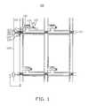
- FIG. 1is a top plan view of part of a first exemplary embodiment of a liquid crystal display (LCD) panel with touch panel function, showing two pixel regions of a second substrate of the LCD panel in full, the LCD panel including a plurality of piezoelectric elements and a plurality of detection lines.
- LCDliquid crystal display
- FIG. 2is a cross section corresponding to line II-II of FIG. 1 .
- FIG. 3is an abbreviated, top plan view of the second substrate of the first exemplary embodiment of the LCD panel, showing, inter alia, an array of the piezoelectric elements and the detection lines.
- FIG. 4is a top plan view of part of a second exemplary embodiment of an LCD panel with touch panel function, showing two pixel regions of a second substrate of the LCD panel in full.
- FIG. 5is a cross section corresponding to line V-V of FIG. 4 .
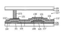
- a first exemplary embodiment of a liquid crystal display (LCD) panel 100 with touch panel functionincludes a first substrate 101 , a second substrate 102 parallel and spaced from the first substrate 101 , and a liquid crystal layer 117 sandwiched between the first substrate 101 and the second substrate 102 .
- LCDliquid crystal display
- a plurality of filter units 104is arranged on a first side of the first substrate 101 that faces toward the liquid crystal layer 117 .
- the filter units 104may for example be red, green, blue, or other colors.
- a plurality of photo spacers 123is formed at the first side of the first substrate 101 .
- the photo spacers 123extend toward the second substrate 102 , and facilitate spacing of the first and the second substrates 101 , 102 from each other.
- the plurality of photo spacers 123can be formed by photolithography.
- a plurality of gates 115 , and a plurality of scan lines 111 parallel to one another,are formed on a second side of the second substrate 102 that faces toward the liquid crystal layer 117 .
- a gate insulating layer 106covers the plurality of gates 115 , the plurality of scan lines 111 , and the second side of the second substrate 102 .
- a plurality of data lines 110 parallel to one another and perpendicular to each of the scan lines 111 , and a semiconductor layer 107are formed on the gate insulating layer 106 .
- a semiconductor doped layer 108is formed on the semiconductor layer 107 .
- a source 130 and a drain 131are located on the semiconductor doped layer 108 in each pixel region.
- a passivation layer 132is formed on the data lines 110 , the sources 130 , and the drains 131 .
- a plurality of rectangular piezoelectric elements 121is formed on the passivation layer 132 , where the data lines 110 cross the scan lines 111 .
- a plurality of pixel electrodes 112is formed on the passivation layer 132 . In each pixel region, the pixel electrode 112 is electrically connected to the drain 131 via a through hole 116 defined in the passivation layer 132 . Ends of the plurality of photo spacers 123 adjacent to the second substrate 102 contact the plurality of piezoelectric elements 121 , respectively.
- the piezoelectric elements 121can be made of shape-memory alloy, superconductive material, piezoelectric ceramic, electrostatic material, magnetostrictive material, mechanochemical gel, or polymer.
- the source 130 , the drain 131 , and the gate 115form a thin film transistor (TFT).
- the source 130is electrically connected to the corresponding data line 110
- the gate 115is electrically connected to the corresponding scan line 111 .
- the first substrate 101When a top of the LCD panel 100 is contacted by, e.g., a user's finger or a stylus, the first substrate 101 deforms. The first substrate 101 applies pressure on one or more of the piezoelectric elements 121 via the corresponding photo spacers 123 . The piezoelectric elements 121 generate electrical signals accordingly. That is, the piezoelectric elements 121 can respond to external pressure applied to the top of the LCD panel 100 , and generate corresponding electrical signals that are input to the detection circuit 124 (see below).
- FIG. 1shows an x-axis and a y-axis of an x-y coordinate system.
- the plurality of piezoelectric elements 121are connected to a detection circuit 124 via a plurality of detection lines 122 extending in the x-axis direction, respectively.
- the detection lines 122may be made of indium tin oxide (ITO) material.
- the detection circuit 124includes at least one detection chip 120 located at each of opposite ends of the second side of the second substrate 102 . In the illustrated embodiment, there is a plurality of detection chips 120 at each of the opposite ends of the second side of the second substrate 102 . At each such end, the detection chips 120 are arranged in a straight line.
- each detection chip 120that receives an input electrical signal (or signals) receives the signal in the form of an analog signal.
- the detection chip 120converts the analog signal to a digital signal, and then sends the digital signal to the controller via a serial bus 125 .
- the controllerprocesses the digital signals from all such detection chips 120 to determine coordinates of a contact point at the top of the LCD panel 100 .
- the number of detection lines 122depends on a touch detection resolution of the LCD panel 100 .
- a multiplicity of the detection lines 122is needed.
- the piezoelectric elements 121are arranged in a regular m ⁇ n array of rows and columns. Each piezoelectric element 121 is connected to a corresponding detection chip 120 via a corresponding detection line 122 .
- two detection chips 120are arranged at opposite ends of each row of the piezoelectric elements 121 .
- Each piezoelectric element 121 in the rowis connected to a corresponding one of the detection chips 120 via an individual dedicated detection line 122 .
- the detection lines 122 corresponding to each row of the piezoelectric elements 121extend from two middlemost piezoelectric elements 121 in the row to each of opposite ends of the row. At each of the two opposite ends of the row, the detection lines 122 are electrically connected to the corresponding detection chip 120 . With this configuration, unwanted influences (such as crosstalk) among the detection lines 122 can be minimized, and a distance between each two adjacent rows of the piezoelectric elements 121 can be reduced.
- the number of detection lines 122 between each two adjacent rows of the piezoelectric elements 121increases from each of the two middlemost piezoelectric elements 121 in each of such rows to each of two endmost piezoelectric elements 121 at each of opposite ends of each such row, respectively. Therefore sizes of the piezoelectric elements 121 in each row progressively decrease from each of the two middlemost piezoelectric elements 121 in each of such rows to each of the two endmost piezoelectric elements 121 at each of the opposite ends of each such row, respectively. With this arrangement, the touch detection resolution of the LCD panel 100 can be greatly improved.
- the plurality of piezoelectric elements 121are arranged at the second substrate 102 , corresponding to the plurality of photo spacers 123 of the LCD panel 100 , respectively.
- the first substrate 101can apply pressure to the plurality of piezoelectric elements 121 , via the plurality of photo spacers 123 pressing the plurality of piezoelectric elements 121 .
- the piezoelectric elements 121output electrical signals to the detection circuit 124 via the corresponding detection lines 122 , and the controller identifies the contact coordinates. Because an external touch panel is not needed, the LCD panel 100 is thinner and lighter.
- the LCD panel 100uses the plurality of piezoelectric elements 121 to provide the touch point identifying function. Accordingly, the LCD panel 100 requires no dedicated extra power supply, and has reduced power consumption.
- a second exemplary embodiment of an LCD panel 200differs from the LCD panel 100 in the following respects.
- a plurality of photo spacers 223is formed a first side of a first substrate 201 that faces toward a second substrate 202 .
- the photo spacers 223are aligned with the TFTs, respectively.
- a plurality of piezoelectric elements 221is sandwiched between tops of the TFTs and the photo spacers 223 , respectively.
- Each piezoelectric element 221outputs a corresponding analog signal to a corresponding detection chip 220 via a corresponding detection line 222 that is arranged parallel to a y axis.
- the piezoelectric elements 121 , 221can have other shapes, such as circular, trapezoidal, triangular, diamond-shaped, etc.
- the detection lines 122 , 222can be bent, curved, or have other forms.
- the piezoelectric elements 121 , 221can be arranged at the first substrates 101 , 201 , with the plurality of photo spacers 123 , 223 formed on the second substrates 102 , 202 and extending toward the first substrates 101 , 201 .
Landscapes
- Engineering & Computer Science (AREA)
- General Engineering & Computer Science (AREA)
- Theoretical Computer Science (AREA)
- Human Computer Interaction (AREA)
- Physics & Mathematics (AREA)
- General Physics & Mathematics (AREA)
- Liquid Crystal (AREA)
- Position Input By Displaying (AREA)
- Devices For Indicating Variable Information By Combining Individual Elements (AREA)
Abstract
Description
Claims (13)
Applications Claiming Priority (3)
| Application Number | Priority Date | Filing Date | Title |
|---|---|---|---|
| CN200810216399ACN101685212B (en) | 2008-09-26 | 2008-09-26 | Liquid crystal display panel |
| CN200810216399 | 2008-09-26 | ||
| CN200810216399.1 | 2008-09-26 |
Publications (2)
| Publication Number | Publication Date |
|---|---|
| US20100079398A1 US20100079398A1 (en) | 2010-04-01 |
| US8334835B2true US8334835B2 (en) | 2012-12-18 |
Family
ID=42048448
Family Applications (1)
| Application Number | Title | Priority Date | Filing Date |
|---|---|---|---|
| US12/586,759Active2030-10-17US8334835B2 (en) | 2008-09-26 | 2009-09-28 | Liquid crystal display panel with touch panel function |
Country Status (2)
| Country | Link |
|---|---|
| US (1) | US8334835B2 (en) |
| CN (1) | CN101685212B (en) |
Cited By (5)
| Publication number | Priority date | Publication date | Assignee | Title |
|---|---|---|---|---|
| US20140145836A1 (en)* | 2010-12-31 | 2014-05-29 | Nokia Corporation | Display apparatus producing audio and haptic output |
| US9030308B1 (en)* | 2010-07-02 | 2015-05-12 | Amazon Technologies, Inc. | Piezoelectric haptic actuator integration |
| US20160202519A1 (en)* | 2015-01-09 | 2016-07-14 | Samsung Display Co., Ltd. | Liquid crystal display having improved lateral visibility |
| US9417754B2 (en) | 2011-08-05 | 2016-08-16 | P4tents1, LLC | User interface system, method, and computer program product |
| US9520036B1 (en)* | 2013-09-18 | 2016-12-13 | Amazon Technologies, Inc. | Haptic output generation with dynamic feedback control |
Families Citing this family (30)
| Publication number | Priority date | Publication date | Assignee | Title |
|---|---|---|---|---|
| CN102467268B (en)* | 2010-10-29 | 2014-02-19 | 北京京东方光电科技有限公司 | Touch screen and manufacture method thereof |
| JP6014308B2 (en)* | 2011-06-08 | 2016-10-25 | 株式会社ジャパンディスプレイ | Display device |
| CN102654681B (en)* | 2012-02-23 | 2016-09-28 | 京东方科技集团股份有限公司 | A kind of display panels and manufacture method thereof and display device |
| US9459160B2 (en) | 2012-06-13 | 2016-10-04 | Microsoft Technology Licensing, Llc | Input device sensor configuration |
| US9684382B2 (en) | 2012-06-13 | 2017-06-20 | Microsoft Technology Licensing, Llc | Input device configuration having capacitive and pressure sensors |
| US9493342B2 (en) | 2012-06-21 | 2016-11-15 | Nextinput, Inc. | Wafer level MEMS force dies |
| EP2870445A1 (en) | 2012-07-05 | 2015-05-13 | Ian Campbell | Microelectromechanical load sensor and methods of manufacturing the same |
| US10578499B2 (en) | 2013-02-17 | 2020-03-03 | Microsoft Technology Licensing, Llc | Piezo-actuated virtual buttons for touch surfaces |
| US20140232679A1 (en)* | 2013-02-17 | 2014-08-21 | Microsoft Corporation | Systems and methods to protect against inadvertant actuation of virtual buttons on touch surfaces |
| US9128566B2 (en) | 2013-02-28 | 2015-09-08 | Acs Co., Ltd. | Acoustic pulse recognition with increased accuracy by localizing contact area of plate |
| US9448631B2 (en) | 2013-12-31 | 2016-09-20 | Microsoft Technology Licensing, Llc | Input device haptics and pressure sensing |
| EP3094950B1 (en) | 2014-01-13 | 2022-12-21 | Nextinput, Inc. | Miniaturized and ruggedized wafer level mems force sensors |
| CN104407466B (en)* | 2014-12-25 | 2017-12-26 | 厦门天马微电子有限公司 | A kind of display base plate, display panel and display device |
| CN104834121B (en)* | 2015-05-11 | 2018-01-30 | 京东方科技集团股份有限公司 | Touch base plate, display panel, display device and touch control method |
| US10416799B2 (en) | 2015-06-03 | 2019-09-17 | Microsoft Technology Licensing, Llc | Force sensing and inadvertent input control of an input device |
| CN107848788B (en) | 2015-06-10 | 2023-11-24 | 触控解决方案股份有限公司 | Ruggedized wafer-level MEMS force sensor with tolerance trench |
| CN105630240B (en)* | 2015-12-23 | 2018-08-07 | 广州中国科学院先进技术研究所 | A kind of multi-point touch panel based on piezoelectric material |
| US10061385B2 (en) | 2016-01-22 | 2018-08-28 | Microsoft Technology Licensing, Llc | Haptic feedback for a touch input device |
| CN105552132B (en)* | 2016-02-04 | 2018-11-13 | 京东方科技集团股份有限公司 | Thin-film transistor sensor and preparation method thereof |
| CN106293235A (en)* | 2016-08-12 | 2017-01-04 | 京东方科技集团股份有限公司 | Sensing arrangement, display floater, driving method and display device |
| EP3580539A4 (en) | 2017-02-09 | 2020-11-25 | Nextinput, Inc. | INTEGRATED DIGITAL FORCE SENSORS AND RELATED METHOD OF MANUFACTURING |
| US11243125B2 (en) | 2017-02-09 | 2022-02-08 | Nextinput, Inc. | Integrated piezoresistive and piezoelectric fusion force sensor |
| US11221263B2 (en) | 2017-07-19 | 2022-01-11 | Nextinput, Inc. | Microelectromechanical force sensor having a strain transfer layer arranged on the sensor die |
| WO2019023309A1 (en) | 2017-07-25 | 2019-01-31 | Nextinput, Inc. | Integrated fingerprint and force sensor |
| WO2019023552A1 (en) | 2017-07-27 | 2019-01-31 | Nextinput, Inc. | A wafer bonded piezoresistive and piezoelectric force sensor and related methods of manufacture |
| WO2019079420A1 (en) | 2017-10-17 | 2019-04-25 | Nextinput, Inc. | Temperature coefficient of offset compensation for force sensor and strain gauge |
| WO2019090057A1 (en) | 2017-11-02 | 2019-05-09 | Nextinput, Inc. | Sealed force sensor with etch stop layer |
| WO2019099821A1 (en) | 2017-11-16 | 2019-05-23 | Nextinput, Inc. | Force attenuator for force sensor |
| US10962427B2 (en) | 2019-01-10 | 2021-03-30 | Nextinput, Inc. | Slotted MEMS force sensor |
| CN110164931B (en)* | 2019-05-23 | 2021-03-30 | 京东方科技集团股份有限公司 | Organic electroluminescent device, method for manufacturing the same, and display device |
Citations (18)
| Publication number | Priority date | Publication date | Assignee | Title |
|---|---|---|---|---|
| JPH11271712A (en) | 1998-03-20 | 1999-10-08 | Toshiba Corp | Liquid crystal display device and position detection device |
| US20020135570A1 (en)* | 2001-03-23 | 2002-09-26 | Seiko Epson Corporation | Coordinate input device detecting touch on board associated with liquid crystal display, and electronic device therefor |
| US6483498B1 (en) | 1999-03-17 | 2002-11-19 | International Business Machines Corporation | Liquid crystal display with integrated resistive touch sensor |
| US6501529B1 (en)* | 1999-08-18 | 2002-12-31 | International Business Machines Corporation | Liquid crystal display element integrated with a touch sensor |
| US20030214541A1 (en)* | 2002-05-16 | 2003-11-20 | Lg.Philips Lcd Co., Ltd. | Apparatus and method for fabricating a liquid crystal display panel |
| US20030214621A1 (en)* | 2002-05-17 | 2003-11-20 | Lg.Philips Lcd Co., Ltd. | Liquid crystal display and a fabricating method thereof |
| US20040263483A1 (en) | 2003-06-24 | 2004-12-30 | Aufderheide Brian E | Sensing device |
| US20050219222A1 (en)* | 2002-04-15 | 2005-10-06 | Koninklijke Philips Electronics N.V. | Touch sensitive display device |
| US20060097373A1 (en)* | 2004-11-11 | 2006-05-11 | Wataru Ito | Electronic device package and electronic equipment |
| US20060192657A1 (en)* | 2005-02-15 | 2006-08-31 | Nec Infrontia Corporation | Electronic apparatus |
| US20070139593A1 (en)* | 2005-12-21 | 2007-06-21 | Industrial Technology Research Institute | Substrate structures, liquid crystal display devices and methods for fabricating liquid crystal display devices |
| US20070222762A1 (en)* | 2004-04-14 | 2007-09-27 | Koninklijke Philips Electronics, N.V. | Touch Sensitive Display |
| US20080030483A1 (en)* | 2006-08-03 | 2008-02-07 | Samsung Electronics Co., Ltd. | Touch screen panel, method of manufacturing the same, and display having the same |
| US20080117182A1 (en) | 2006-11-17 | 2008-05-22 | Samsung Electronics Co., Ltd. | Display device including sensing elements and driving method thereof |
| US20080122315A1 (en)* | 2006-11-15 | 2008-05-29 | Sony Corporation | Substrate supporting vibration structure, input device having haptic function, and electronic device |
| US20080180615A1 (en)* | 2007-01-25 | 2008-07-31 | Seiko Epson Corporation | Liquid crystal display device and electronic apparatus |
| TWI303774B (en) | 2004-12-28 | 2008-12-01 | Seiko Epson Corp | Touch panel device |
| US20100013785A1 (en)* | 2007-03-01 | 2010-01-21 | Atsuhito Murai | Display panel substrate, display panel, display appratus, and method for manufacturing display panel substrate |
- 2008
- 2008-09-26CNCN200810216399Apatent/CN101685212B/enactiveActive
- 2009
- 2009-09-28USUS12/586,759patent/US8334835B2/enactiveActive
Patent Citations (19)
| Publication number | Priority date | Publication date | Assignee | Title |
|---|---|---|---|---|
| JPH11271712A (en) | 1998-03-20 | 1999-10-08 | Toshiba Corp | Liquid crystal display device and position detection device |
| US6483498B1 (en) | 1999-03-17 | 2002-11-19 | International Business Machines Corporation | Liquid crystal display with integrated resistive touch sensor |
| US6501529B1 (en)* | 1999-08-18 | 2002-12-31 | International Business Machines Corporation | Liquid crystal display element integrated with a touch sensor |
| US20020135570A1 (en)* | 2001-03-23 | 2002-09-26 | Seiko Epson Corporation | Coordinate input device detecting touch on board associated with liquid crystal display, and electronic device therefor |
| US20050219222A1 (en)* | 2002-04-15 | 2005-10-06 | Koninklijke Philips Electronics N.V. | Touch sensitive display device |
| US20030214541A1 (en)* | 2002-05-16 | 2003-11-20 | Lg.Philips Lcd Co., Ltd. | Apparatus and method for fabricating a liquid crystal display panel |
| US20030214621A1 (en)* | 2002-05-17 | 2003-11-20 | Lg.Philips Lcd Co., Ltd. | Liquid crystal display and a fabricating method thereof |
| CN1860432A (en) | 2003-06-24 | 2006-11-08 | 3M创新有限公司 | Sensing device |
| US20040263483A1 (en) | 2003-06-24 | 2004-12-30 | Aufderheide Brian E | Sensing device |
| US20070222762A1 (en)* | 2004-04-14 | 2007-09-27 | Koninklijke Philips Electronics, N.V. | Touch Sensitive Display |
| US20060097373A1 (en)* | 2004-11-11 | 2006-05-11 | Wataru Ito | Electronic device package and electronic equipment |
| TWI303774B (en) | 2004-12-28 | 2008-12-01 | Seiko Epson Corp | Touch panel device |
| US20060192657A1 (en)* | 2005-02-15 | 2006-08-31 | Nec Infrontia Corporation | Electronic apparatus |
| US20070139593A1 (en)* | 2005-12-21 | 2007-06-21 | Industrial Technology Research Institute | Substrate structures, liquid crystal display devices and methods for fabricating liquid crystal display devices |
| US20080030483A1 (en)* | 2006-08-03 | 2008-02-07 | Samsung Electronics Co., Ltd. | Touch screen panel, method of manufacturing the same, and display having the same |
| US20080122315A1 (en)* | 2006-11-15 | 2008-05-29 | Sony Corporation | Substrate supporting vibration structure, input device having haptic function, and electronic device |
| US20080117182A1 (en) | 2006-11-17 | 2008-05-22 | Samsung Electronics Co., Ltd. | Display device including sensing elements and driving method thereof |
| US20080180615A1 (en)* | 2007-01-25 | 2008-07-31 | Seiko Epson Corporation | Liquid crystal display device and electronic apparatus |
| US20100013785A1 (en)* | 2007-03-01 | 2010-01-21 | Atsuhito Murai | Display panel substrate, display panel, display appratus, and method for manufacturing display panel substrate |
Cited By (61)
| Publication number | Priority date | Publication date | Assignee | Title |
|---|---|---|---|---|
| US9030308B1 (en)* | 2010-07-02 | 2015-05-12 | Amazon Technologies, Inc. | Piezoelectric haptic actuator integration |
| US20140145836A1 (en)* | 2010-12-31 | 2014-05-29 | Nokia Corporation | Display apparatus producing audio and haptic output |
| US9389688B2 (en)* | 2010-12-31 | 2016-07-12 | Nokia Technologies Oy | Display apparatus producing audio and haptic output |
| US9417754B2 (en) | 2011-08-05 | 2016-08-16 | P4tents1, LLC | User interface system, method, and computer program product |
| US10013094B1 (en) | 2011-08-05 | 2018-07-03 | P4tents1, LLC | System, method, and computer program product for a multi-pressure selection touch screen |
| US10013095B1 (en) | 2011-08-05 | 2018-07-03 | P4tents1, LLC | Multi-type gesture-equipped touch screen system, method, and computer program product |
| US10031607B1 (en) | 2011-08-05 | 2018-07-24 | P4tents1, LLC | System, method, and computer program product for a multi-pressure selection touch screen |
| US10120480B1 (en) | 2011-08-05 | 2018-11-06 | P4tents1, LLC | Application-specific pressure-sensitive touch screen system, method, and computer program product |
| US10133397B1 (en) | 2011-08-05 | 2018-11-20 | P4tents1, LLC | Tri-state gesture-equipped touch screen system, method, and computer program product |
| US10146353B1 (en) | 2011-08-05 | 2018-12-04 | P4tents1, LLC | Touch screen system, method, and computer program product |
| US10156921B1 (en) | 2011-08-05 | 2018-12-18 | P4tents1, LLC | Tri-state gesture-equipped touch screen system, method, and computer program product |
| US10162448B1 (en) | 2011-08-05 | 2018-12-25 | P4tents1, LLC | System, method, and computer program product for a pressure-sensitive touch screen for messages |
| US10203794B1 (en) | 2011-08-05 | 2019-02-12 | P4tents1, LLC | Pressure-sensitive home interface system, method, and computer program product |
| US10209809B1 (en) | 2011-08-05 | 2019-02-19 | P4tents1, LLC | Pressure-sensitive touch screen system, method, and computer program product for objects |
| US10209807B1 (en) | 2011-08-05 | 2019-02-19 | P4tents1, LLC | Pressure sensitive touch screen system, method, and computer program product for hyperlinks |
| US10209808B1 (en) | 2011-08-05 | 2019-02-19 | P4tents1, LLC | Pressure-based interface system, method, and computer program product with virtual display layers |
| US10209806B1 (en) | 2011-08-05 | 2019-02-19 | P4tents1, LLC | Tri-state gesture-equipped touch screen system, method, and computer program product |
| US10222891B1 (en) | 2011-08-05 | 2019-03-05 | P4tents1, LLC | Setting interface system, method, and computer program product for a multi-pressure selection touch screen |
| US10222895B1 (en) | 2011-08-05 | 2019-03-05 | P4tents1, LLC | Pressure-based touch screen system, method, and computer program product with virtual display layers |
| US10222892B1 (en) | 2011-08-05 | 2019-03-05 | P4tents1, LLC | System, method, and computer program product for a multi-pressure selection touch screen |
| US10222894B1 (en) | 2011-08-05 | 2019-03-05 | P4tents1, LLC | System, method, and computer program product for a multi-pressure selection touch screen |
| US10222893B1 (en) | 2011-08-05 | 2019-03-05 | P4tents1, LLC | Pressure-based touch screen system, method, and computer program product with virtual display layers |
| US10275086B1 (en) | 2011-08-05 | 2019-04-30 | P4tents1, LLC | Gesture-equipped touch screen system, method, and computer program product |
| US10275087B1 (en) | 2011-08-05 | 2019-04-30 | P4tents1, LLC | Devices, methods, and graphical user interfaces for manipulating user interface objects with visual and/or haptic feedback |
| US10338736B1 (en) | 2011-08-05 | 2019-07-02 | P4tents1, LLC | Devices, methods, and graphical user interfaces for manipulating user interface objects with visual and/or haptic feedback |
| US10345961B1 (en) | 2011-08-05 | 2019-07-09 | P4tents1, LLC | Devices and methods for navigating between user interfaces |
| US10365758B1 (en) | 2011-08-05 | 2019-07-30 | P4tents1, LLC | Devices, methods, and graphical user interfaces for manipulating user interface objects with visual and/or haptic feedback |
| US10386960B1 (en) | 2011-08-05 | 2019-08-20 | P4tents1, LLC | Devices, methods, and graphical user interfaces for manipulating user interface objects with visual and/or haptic feedback |
| US10521047B1 (en) | 2011-08-05 | 2019-12-31 | P4tents1, LLC | Gesture-equipped touch screen system, method, and computer program product |
| US10534474B1 (en) | 2011-08-05 | 2020-01-14 | P4tents1, LLC | Gesture-equipped touch screen system, method, and computer program product |
| US10540039B1 (en) | 2011-08-05 | 2020-01-21 | P4tents1, LLC | Devices and methods for navigating between user interface |
| US10551966B1 (en) | 2011-08-05 | 2020-02-04 | P4tents1, LLC | Gesture-equipped touch screen system, method, and computer program product |
| US10592039B1 (en) | 2011-08-05 | 2020-03-17 | P4tents1, LLC | Gesture-equipped touch screen system, method, and computer program product for displaying multiple active applications |
| US10606396B1 (en) | 2011-08-05 | 2020-03-31 | P4tents1, LLC | Gesture-equipped touch screen methods for duration-based functions |
| US10642413B1 (en) | 2011-08-05 | 2020-05-05 | P4tents1, LLC | Gesture-equipped touch screen system, method, and computer program product |
| US10649578B1 (en) | 2011-08-05 | 2020-05-12 | P4tents1, LLC | Gesture-equipped touch screen system, method, and computer program product |
| US10649580B1 (en) | 2011-08-05 | 2020-05-12 | P4tents1, LLC | Devices, methods, and graphical use interfaces for manipulating user interface objects with visual and/or haptic feedback |
| US10649579B1 (en) | 2011-08-05 | 2020-05-12 | P4tents1, LLC | Devices, methods, and graphical user interfaces for manipulating user interface objects with visual and/or haptic feedback |
| US10649571B1 (en) | 2011-08-05 | 2020-05-12 | P4tents1, LLC | Devices, methods, and graphical user interfaces for manipulating user interface objects with visual and/or haptic feedback |
| US10649581B1 (en) | 2011-08-05 | 2020-05-12 | P4tents1, LLC | Devices, methods, and graphical user interfaces for manipulating user interface objects with visual and/or haptic feedback |
| US10656756B1 (en) | 2011-08-05 | 2020-05-19 | P4tents1, LLC | Gesture-equipped touch screen system, method, and computer program product |
| US10656757B1 (en) | 2011-08-05 | 2020-05-19 | P4tents1, LLC | Gesture-equipped touch screen system, method, and computer program product |
| US10656754B1 (en) | 2011-08-05 | 2020-05-19 | P4tents1, LLC | Devices and methods for navigating between user interfaces |
| US10656752B1 (en) | 2011-08-05 | 2020-05-19 | P4tents1, LLC | Gesture-equipped touch screen system, method, and computer program product |
| US10656755B1 (en) | 2011-08-05 | 2020-05-19 | P4tents1, LLC | Gesture-equipped touch screen system, method, and computer program product |
| US10656753B1 (en) | 2011-08-05 | 2020-05-19 | P4tents1, LLC | Gesture-equipped touch screen system, method, and computer program product |
| US10656759B1 (en) | 2011-08-05 | 2020-05-19 | P4tents1, LLC | Devices, methods, and graphical user interfaces for manipulating user interface objects with visual and/or haptic feedback |
| US10656758B1 (en) | 2011-08-05 | 2020-05-19 | P4tents1, LLC | Gesture-equipped touch screen system, method, and computer program product |
| US10664097B1 (en) | 2011-08-05 | 2020-05-26 | P4tents1, LLC | Devices, methods, and graphical user interfaces for manipulating user interface objects with visual and/or haptic feedback |
| US10671212B1 (en) | 2011-08-05 | 2020-06-02 | P4tents1, LLC | Gesture-equipped touch screen system, method, and computer program product |
| US10671213B1 (en) | 2011-08-05 | 2020-06-02 | P4tents1, LLC | Devices, methods, and graphical user interfaces for manipulating user interface objects with visual and/or haptic feedback |
| US10725581B1 (en) | 2011-08-05 | 2020-07-28 | P4tents1, LLC | Devices, methods and graphical user interfaces for manipulating user interface objects with visual and/or haptic feedback |
| US10782819B1 (en) | 2011-08-05 | 2020-09-22 | P4tents1, LLC | Gesture-equipped touch screen system, method, and computer program product |
| US10788931B1 (en) | 2011-08-05 | 2020-09-29 | P4tents1, LLC | Devices, methods, and graphical user interfaces for manipulating user interface objects with visual and/or haptic feedback |
| US10838542B1 (en) | 2011-08-05 | 2020-11-17 | P4tents1, LLC | Gesture-equipped touch screen system, method, and computer program product |
| US10936114B1 (en) | 2011-08-05 | 2021-03-02 | P4tents1, LLC | Gesture-equipped touch screen system, method, and computer program product |
| US10996787B1 (en) | 2011-08-05 | 2021-05-04 | P4tents1, LLC | Gesture-equipped touch screen system, method, and computer program product |
| US11061503B1 (en) | 2011-08-05 | 2021-07-13 | P4tents1, LLC | Devices, methods, and graphical user interfaces for manipulating user interface objects with visual and/or haptic feedback |
| US11740727B1 (en) | 2011-08-05 | 2023-08-29 | P4Tents1 Llc | Devices, methods, and graphical user interfaces for manipulating user interface objects with visual and/or haptic feedback |
| US9520036B1 (en)* | 2013-09-18 | 2016-12-13 | Amazon Technologies, Inc. | Haptic output generation with dynamic feedback control |
| US20160202519A1 (en)* | 2015-01-09 | 2016-07-14 | Samsung Display Co., Ltd. | Liquid crystal display having improved lateral visibility |
Also Published As
| Publication number | Publication date |
|---|---|
| US20100079398A1 (en) | 2010-04-01 |
| CN101685212A (en) | 2010-03-31 |
| CN101685212B (en) | 2012-08-29 |
Similar Documents
| Publication | Publication Date | Title |
|---|---|---|
| US8334835B2 (en) | Liquid crystal display panel with touch panel function | |
| US10572062B2 (en) | Display device and touch detection method of display device | |
| US8659564B2 (en) | Touch sensible display device having reduced number of image data lines | |
| CN103034377B (en) | Embedded touch panel | |
| KR101564332B1 (en) | Touch screen panel integrated into a liquid crystal display, manufacturing method thereof, and touch sensing method | |
| CN106775165B (en) | Embedded touch display panel and electronic device | |
| CN101825787B (en) | Touch display screen and manufacture method thereof | |
| US8279361B2 (en) | Touch-sensitive liquid crystal display device | |
| US9013434B2 (en) | Touch display panel and driving method thereof | |
| CN105183220B (en) | Touch display device and driving method thereof | |
| CN103926729A (en) | Array substrate, color film substrate, touch display device and driving method thereof | |
| CN104570446B (en) | A kind of touch-control display panel and its control method | |
| US20120162109A1 (en) | Display apparatus | |
| CN101900903B (en) | Liquid crystal display panel and liquid crystal display apparatus | |
| US20110096019A1 (en) | Touch panel and touch display device | |
| US9019221B2 (en) | Display device integrated with touch screen panel | |
| JP2020140085A (en) | In-cell touch panel | |
| CN205721693U (en) | A kind of touch-control display panel and touch control display apparatus | |
| KR20070047956A (en) | Manufacturing Method of Display Board | |
| CN101593069A (en) | Resistance type touch control display panel | |
| CN110134289B (en) | Pixel array substrate and driving method thereof | |
| JP2007058070A (en) | Liquid crystal display apparatus | |
| CN117991552A (en) | Array substrate, manufacturing method thereof and display panel | |
| TWI489366B (en) | Resistance type touch display panel | |
| TWI848736B (en) | Touch display panel |
Legal Events
| Date | Code | Title | Description |
|---|---|---|---|
| AS | Assignment | Owner name:INNOLUX DISPLAY CORP.,TAIWAN Free format text:ASSIGNMENT OF ASSIGNORS INTEREST;ASSIGNORS:SHEN, HUNG-MING;CHO, HUNG-SHENG;REEL/FRAME:023343/0169 Effective date:20090923 Owner name:INNOLUX DISPLAY CORP., TAIWAN Free format text:ASSIGNMENT OF ASSIGNORS INTEREST;ASSIGNORS:SHEN, HUNG-MING;CHO, HUNG-SHENG;REEL/FRAME:023343/0169 Effective date:20090923 | |
| AS | Assignment | Owner name:CHIMEI INNOLUX CORPORATION, TAIWAN Free format text:CHANGE OF NAME;ASSIGNOR:INNOLUX DISPLAY CORPORATION;REEL/FRAME:027560/0887 Effective date:20100330 | |
| STCF | Information on status: patent grant | Free format text:PATENTED CASE | |
| AS | Assignment | Owner name:INNOLUX CORPORATION, TAIWAN Free format text:CHANGE OF NAME;ASSIGNOR:CHIMEI INNOLUX CORPORATION;REEL/FRAME:032672/0813 Effective date:20121219 | |
| FPAY | Fee payment | Year of fee payment:4 | |
| MAFP | Maintenance fee payment | Free format text:PAYMENT OF MAINTENANCE FEE, 8TH YEAR, LARGE ENTITY (ORIGINAL EVENT CODE: M1552); ENTITY STATUS OF PATENT OWNER: LARGE ENTITY Year of fee payment:8 | |
| MAFP | Maintenance fee payment | Free format text:PAYMENT OF MAINTENANCE FEE, 12TH YEAR, LARGE ENTITY (ORIGINAL EVENT CODE: M1553); ENTITY STATUS OF PATENT OWNER: LARGE ENTITY Year of fee payment:12 | |
| AS | Assignment | Owner name:RED OAK INNOVATIONS LIMITED, IRELAND Free format text:ASSIGNMENT OF ASSIGNORS INTEREST;ASSIGNOR:INNOLUX CORPORATION;REEL/FRAME:069206/0903 Effective date:20240925 |