US8333839B2 - Vapor deposition reactor - Google Patents
Vapor deposition reactorDownload PDFInfo
- Publication number
- US8333839B2 US8333839B2US11/965,235US96523507AUS8333839B2US 8333839 B2US8333839 B2US 8333839B2US 96523507 AUS96523507 AUS 96523507AUS 8333839 B2US8333839 B2US 8333839B2
- Authority
- US
- United States
- Prior art keywords
- space
- reactor
- vapor deposition
- reactant
- purge gas
- Prior art date
- Legal status (The legal status is an assumption and is not a legal conclusion. Google has not performed a legal analysis and makes no representation as to the accuracy of the status listed.)
- Expired - Fee Related, expires
Links
Images


Classifications
- C—CHEMISTRY; METALLURGY
- C23—COATING METALLIC MATERIAL; COATING MATERIAL WITH METALLIC MATERIAL; CHEMICAL SURFACE TREATMENT; DIFFUSION TREATMENT OF METALLIC MATERIAL; COATING BY VACUUM EVAPORATION, BY SPUTTERING, BY ION IMPLANTATION OR BY CHEMICAL VAPOUR DEPOSITION, IN GENERAL; INHIBITING CORROSION OF METALLIC MATERIAL OR INCRUSTATION IN GENERAL
- C23C—COATING METALLIC MATERIAL; COATING MATERIAL WITH METALLIC MATERIAL; SURFACE TREATMENT OF METALLIC MATERIAL BY DIFFUSION INTO THE SURFACE, BY CHEMICAL CONVERSION OR SUBSTITUTION; COATING BY VACUUM EVAPORATION, BY SPUTTERING, BY ION IMPLANTATION OR BY CHEMICAL VAPOUR DEPOSITION, IN GENERAL
- C23C16/00—Chemical coating by decomposition of gaseous compounds, without leaving reaction products of surface material in the coating, i.e. chemical vapour deposition [CVD] processes
- C23C16/44—Chemical coating by decomposition of gaseous compounds, without leaving reaction products of surface material in the coating, i.e. chemical vapour deposition [CVD] processes characterised by the method of coating
- C23C16/455—Chemical coating by decomposition of gaseous compounds, without leaving reaction products of surface material in the coating, i.e. chemical vapour deposition [CVD] processes characterised by the method of coating characterised by the method used for introducing gases into reaction chamber or for modifying gas flows in reaction chamber
- C23C16/45523—Pulsed gas flow or change of composition over time
- C23C16/45525—Atomic layer deposition [ALD]
- C23C16/45544—Atomic layer deposition [ALD] characterized by the apparatus
- C23C16/45548—Atomic layer deposition [ALD] characterized by the apparatus having arrangements for gas injection at different locations of the reactor for each ALD half-reaction
- C23C16/45551—Atomic layer deposition [ALD] characterized by the apparatus having arrangements for gas injection at different locations of the reactor for each ALD half-reaction for relative movement of the substrate and the gas injectors or half-reaction reactor compartments
Definitions
- the present inventionrelates to a reactor used for a vapor deposition scheme.
- ALDatomic layer deposition
- ALDinjects, as shown in FIG. 1 , one or more precursors into a reactor and carries out a purge/pump of the precursor to maintain or leave one or more molecule layers on a substrate. Then it injects one or more reactants into the reactor and carries out a purge/pump to obtain one or more mono-atomic reacted layers. Therefore, one or more mono-atomic layers are formed through one cycle consisting of four steps.
- a conventional ALD reactoradopts a cross-flow scheme (this is also called as a ‘traveling-wave’ scheme) where a precursor, a reactant, a purge gas and the like are injected parallely to the surface of a target substrate for deposition, or a shower-head scheme where a precursor, a reactant, a purge gas and the like are injected perpendicularly to the surface of a target substrate for deposition.
- FIG. 2illustrates a cross-flow ALD reactor
- FIG. 3illustrates a shower-head ALD reactor.
- precursorsare injected parallely to the surface of a substrate as depicted in FIG. 2 , so all the precursors do not necessarily reach the substrate at the same time, but a substrate near an injection port experiences an adsorption phenomenon first, followed by a substrate on the side of an exhaust port later on.
- adsorptioncan be expressed as a function of time.
- compositionsmay vary or film properties may be changed according to the locations of an injection port and an exhaust port.
- an injection port(sub-injection ports to be more specific) is spaced apart from a substrate by a uniform distance as depicted in FIG. 3 , so precursors adsorb at the surface of the substrate almost at the same time.
- the shower-head schemecompared with the cross-flow scheme, can be advantageously used for obtaining a thin film having homogenous properties.
- a reactor using such a shower-head injection porthas a large volume so that it takes long to carry out a purge/pumping process and uses a large amount of precursors and reactants.
- ALD reactorsperiodically receive a precursor, a reactant, and a purge gas therein via a valve.
- a valveoperates at high speed and at high frequencies. For instance, in order to deposit a 1 ⁇ m-atomic layer, the valve needs to operate 10,000 times or more for each process. This actually causes problems related to the lifespan of a valve.
- both ALD reactors of the prior artare designed to be rather difficult for the application of remote plasma, the use of high frequencies including microwave, UV irradiation and so on.
- an object of the present inventionto provide a vapor deposition reactor that exhibits homogeneous film properties yet has an improved deposition efficiency of precursors and a substantially reduced time required for a purge/pumping process.
- a vapor deposition reactorhaving a configuration where a substrate or a vapor deposition reactor moves in a non-contact state with each other to allow the substrate to pass by the reactor, and an injection unit and an exhaust unit are installed as a basic module of the reactor for receiving a precursor or a reactant and for receiving and pumping a purge gas, respectively.
- FIG. 1illustrates 4 successive steps of atomic layer deposition (ALD).
- FIG. 2illustrates a conventional cross-flow ALD reactor.
- FIG. 3illustrates a conventional shower-head ALD reactor.
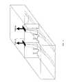
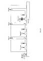
- FIG. 4illustrates a basic module of a reactor according to an embodiment of the present invention.
- FIG. 5illustrates an ALD reactor provided with two basic modules shown in FIG. 4 .
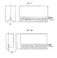
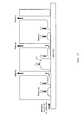
- FIG. 6illustrates a schematic overall view of the ALD reactor shown in FIG. 5 .
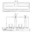
- FIG. 7is a lateral cross-sectional view of an injection unit 511 of a first module 51 shown in FIG. 5 .
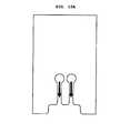
- FIGS. 8A through 8Drespectively illustrate lateral cross-sectional views, a plan view, and a bottom view of an exhaust unit 512 of the first module 51 shown in FIG. 5 .
- FIG. 9indicates parameters of the ALD reactor shown in FIG. 5 .
- FIGS. 10A , 10 B and FIGS. 11A , 11 Brespectively illustrate an injection unit consisting of two injection ports.
- FIG. 12illustrates a reactor performing a 2-step reaction to form an atomic layer.
- FIG. 13illustrates two modules used for injecting and exhausting a precursor.
- FIG. 14illustrates a reactor, in which two-atomic layers are deposited every time a substrate passes by the reactor.
- FIG. 15illustrates a reactor comprising a cooling/heating means.
- FIGS. 16 through 18respectively illustrate a reactor comprising a means for direct UV irradiation.
- FIGS. 19 through 21respectively illustrate a reactor comprising a means for indirect UV irradiation.
- FIGS. 22 through 25respectively illustrate a reactor comprising a means for plasma applications.
- FIGS. 26 and 27respectively illustrate a reactor comprising a means for microwave applications.
- a vapor deposition reactorhas a configuration where a substrate or a vapor deposition reactor moves in non-contact state with each other to allow the substrate to pass by the reactor.
- a portion of the reactor being open to the substrateis a place where a precursor, a purge gas, or a reactant outflows from the reactor.
- a basic module of a vapor deposition reactoris provided with an injection unit 41 and an exhaust unit 42 .
- either the vapor deposition reactor or a substrate belowmoves in order to make a portion of the substrate having passed by the injection unit 41 pass by the exhaust unit 42 next.
- the vapor deposition reactor or the substratemay move linearly or rotatably. The following description will be directed to the linear movement of a substrate for convenience of explanation.
- FIG. 5illustrates an ALD reactor using two of the present invention basic modules shown in FIG. 4 .
- a precursoris injected into an injection unit 511 of a first module 51 , and a purge gas is injected into an exhaust unit 512 of the first module 51 and then purged/pumped.
- a reactantis injected into an injection unit 521 of a second module 52 , and a purge gas is injected into an exhaust unit 522 of the second module 52 and then purged/pumped.
- a substratesuccessively passes by the injection unit 511 of the first module 51 ⁇ the exhaust unit 512 of the first module 51 ⁇ the injection unit 521 of the second module 52 ⁇ the exhaust unit 522 of the second module 52 , operating on a 4 step cycle to form an atomic layer on the substrate.
- FIG. 6illustrates a schematic overall view of the ALD reactor shown in FIG. 5 .
- FIG. 7is a lateral cross-sectional view of an injection unit 511 of the first module 51 shown in FIG. 5 .
- FIG. 8Ais a lateral cross-sectional view of the exhaust unit 512 of the first module 51 shown in FIG. 5 , taken along line A-A
- FIG. 8Bis a lateral cross-sectional view of the exhaust unit 512 of the first module 51 , taken along line B-B.
- the lateral facesare curved.
- FIG. 8Cis a plan view of the exhaust unit 512 of the first module 51 shown in FIG. 5 , and FIG.
- FIG. 8Dis a bottom view of the exhaust unit 512 of the first module 51 shown in FIG. 5 .
- the injection unit 521 and the exhaust unit 522 of the second module 52are identical in shape with the injection unit 511 and the exhaust unit 512 of the first module 51 .
- injectorsmay be designed to have holes of varying sizes.
- a precursor, a purge gas, and a reactantmay be injected with a pipe-shaped channel through a lateral face as depicted in the drawings attached to this specification, or may be injected with a pipe-shaped channel from the top.
- sizes/spacings of the structural components of the ALD reactor and movement speed of a substratecan be changed by adjusting parameters.
- a precursorfills a space at a portion of the injection unit 511 with a width x 0 in the first module 51 when a substrate passes under the reactor.
- the spacing z 1 between the reactor and the substrate at the injection unit 511 of the first module 51is small, the target space is filled with precursors with a little leakage. That is, a sufficient amount of precursors can be supplied to the substrate if the width x 0 is made large, but the chances of adsorbing precursors on the substrate get lower if the width x 0 is made small.
- x 0is set variably corresponding to the characteristics of a precursor to be used.
- precursors having been adsorbed on the surface of the substrateleave a chemically adsorbed molecular layer by injection and pumping of a purge gas (nitrogen or argon). Meanwhile, if the movement speed v of the substrate is made faster or the width xi of the reactor is made smaller for the intention of leaving some of precursors, not only a chemically adsorbed molecular layer but also part of a physical adsorption layer remain on the surface of the substrate for use in deposition.
- a purge gasnitrogen or argon
- a chemically adsorbed molecular layeris left on the surface of the substrate as the substrate passes by the injection unit 511 and the exhaust unit 512 of the first module 51 .
- a reactantis injected when the substrate passes by the injection unit 521 of the second module 52 for the reactor, and is purged/pumped when the substrate passes by the exhaust unit 522 of the second module 52 .
- one or more atomic layersare formed on the substrate through the 4-step cycle of ALD, without any help from a valve or a similar product.
- the substratebeing in a non-contact state separated from the reactor by a designated spacing z and moving at the speed of v, passes by the injection unit 511 (width, x 0 ) of the first module 51 , a precursor is injected and a chemical adsorption layer and a physical adsorption layer are formed on the surface of the substrate.
- a physical adsorption layerwhose molecules are held together by a weak force or the Van der Waals attraction is separated from the substrate by a purge gas and is removed by pumping later. This leaves only a chemical adsorption layer on the surface of the substrate.
- a reactantis injected to substitute a part of the chemical adsorption layer existing on the surface of the substrate.
- a desired atomic layeris formed on the surface of the substrate, and any surplus reactant remains in a physically adsorbed state.
- the physically adsorbed reactant having a weak intermolecular forceis removed by a purge/pumping and a mono-atomic layer is formed on the surface of the substrate at the end.
- an inlet for injecting a precursor, a purge gas, or a reactantshows the typical shape of a fine hole with a diameter of 1-2 mm, but this size is also adjustable corresponding to the size of a substrate.
- guardsserve to isolate the respective step and to maximize the deposition efficiency of precursors while preventing a precursor leak.
- the guard width L 1 -L 5is variable depending on the width x 0 , x 1 , x 2 , and x 3 of the injection unit in each of the 4 steps for ALD.
- the spacing z 1 between the first guard (width, L 1 ) of the first module 51 where the first step of ALD is performedmay be set differently from the spacing Z 3 between the third guard (width, L 3 ) of the second module 52 where the third step of ALD is performed.
- the configuration of the reactormay be designed in different ways by modifying its basic modules to meet diverse needs, for example, when more than two kinds of precursors need to be injected or when a reaction of more than two steps is carried out to form an atomic layer, etc.
- FIGS. 10 and 11illustrate an injection unit with two inlets for a reactor module, wherein the inlets are respectively used for receiving two different kinds of precursors or reactants that do not interact with each other.
- two inletsare arranged side by side (see FIG. 10B ), in which 10 - 1 is an inlet for a first precursor and 10 - 2 is an inlet for a second precursor.
- two inletsare arranged alternately one after another in a line (see FIG. 11B ), in which 11 - 1 is an inlet for a first precursor and 11 - 2 is an inlet for a second precursor.
- FIG. 10 or FIG. 11more than two different kinds of precursors or reactants can be fed or injected at the same time.
- FIG. 12illustrates a reactor performing a 2-step reaction to form an atomic layer.
- the reactorhas three basic modules, where two of them are used for receiving and exhausting a reactant. For instance, an organic metal precursor is first injected to adsorb organic metal molecules on the surface of a substrate, and hydrogen atoms are then injected to substitute the organic metal molecules to a metal hydride. After that, nitrogen atoms are injected to induce a secondary reaction for producing a metal nitride.
- FIG. 13illustrates a reactor having two modules for receiving and exhausting precursors.
- a precursor not having the self-limiting naturee.g., TiCl 4 or SiH 4
- the 4-step cycle of ALDhad to be repeated several times to form a mono-atomic layer only.
- a reactoris designed to have several precursor injection and exhaust modules and one reactant injection unit and exhaust unit at the end. Therefore, it only requires a substrate to pass by the reactor once for forming a mono-atomic layer.
- FIG. 14illustrates a reactor, in which two-atomic layers are deposited every time a substrate passes by the reactor.
- a homogeneous filmis formed.
- a TiO 2 atomic layeris to be formed by using a precursor containing metal Ti atoms
- a homogeneous thin film like TiO 2 +TiO 2 or TiN+TiNcan be formed.
- a heterogenous thin film made out of a material containing the same metal atomscan be formed.
- a heterogeneous thin film like TiN+TiO 2 or TiO 2 +TiNcan be formed.
- the use of different precursorsmay be followed by the formation of atomic layers of two different kinds.
- a heterogeneous oxide film like TiO 2 +SiO 2 or a heterogenous thin film like AlN+SiO 2can be formed.
- the reactor according to an embodiment of the present inventionmay be configured to include a cooling and heating means, a UV irradiation means, a plasma application means, and a super high frequency application means.
- FIG. 15illustrates a reactor provided with a cooling means or a heating means.
- Reference numeral 151denotes a cooling/heating means.
- a cooling processis required for keeping an increased vapor pressure of a precursor caused by precursor decomposition at the time of supply at the same temperature as a reactor (or reactor body), or for cooling down a reactor having been heated by a plasma or UV catalytic reaction.
- a heating processis required to keep the reactor (or reactor body) at a high temperature especially when a precursor was condensed at a low temperature or vapor pressure of the precursor was lowered.
- a proper heating temperatureneeds to be set in order to prevent any changes in the process results after a precursor was condensed instead of being decomposed or after vapor pressure of the precursor was lowered.
- the heating temperatureis variable according to precursor materials being used, it can be within a range from 70 to 150° C. Heat rays are utilized as the heating means, and measurement control is done by a thermocouple.
- FIGS. 16 through 18respectively illustrate a reactor provided with a means for direct UV irradiation.
- Reference numerals 161 , 171 , and 181 in the drawingsdenote a UV irradiation means.
- UV rays of a specific wavelength or beloware irradiated onto the substrate for inducing a complete reaction.
- FIG. 16depicts that UV rays are irradiated onto the adsorbed molecular layer to destroy an intermolecular bonding and a bonding between a metal atom and a molecule.
- FIG. 17depicts that UV rays activate a reactant to induce a more activated reaction or a complete reaction.
- FIG. 18depicts that some of the molecular bonds adsorbed at the surface of a substrate are taken off by UV rays and react with an injected reactant to induce a complete reaction or a multi-step reaction.
- FIGS. 19 through 21respectively illustrate a reactor provided with a means for indirect UV irradiation.
- Reference numerals 191 , 201 , 211 , and 212 in the drawingsdenote a UV irradiation means. It is useful when UV rays should not be irradiated directly onto a substrate if the substrate is easily deformed or denatured by UV rays.
- FIG. 19shows a case where the activity of a reactant is too large, so the reactant is activated by UV rays in a separate space and the remotely generated activated atoms or radicals are injected into a substrate to induce a complete reaction.
- FIGS. 20 and 21respectively illustrate a reactor having a down-stream UV reaction chamber and a purge/pumping chamber.
- a reactantis activated to a radical state and is fed towards a substrate by means of a carrier gas, so more than one kind of reactant can be activated.
- two kinds of reactantsare utilized to form a thin film.
- the reactor of FIG. 21resolves such problems by respectively activating those two kinds of reactants to a desired level by UV lamps of different wavelengths to form a thin film.
- different kinds of reactantsare mixed and form a new compound, or activity may be decreased. Even in that case, the reactors of FIGS. 20 and 21 can be advantageously used for separating the mixed reactants.
- an injection unithaving the structure shown in FIG. 10 or FIG. 11 may be employed to prevent reactants from mixing together.
- FIGS. 22 through 25respectively illustrate a reactor provided with a plasma application means.
- Reference numerals 221 , 231 , 241 , and 251 in the drawingsdenote a plasma application means.
- FIG. 22shows a reactor having a concentric type plasma generation device for generating homogeneous plasma, and downstream radicals.
- FIG. 23shows a reactor having a plasma generating space where plasma is generated exclusively and become downstream plasma radicals.
- FIGS. 24 and 25respectively show a reactor having a plasma application means for multi-step reactions.
- FIGS. 26 and 27respectively illustrate a reactor provided with a super high frequency application means.
- Reference numerals 261 and 271 in the drawingsdenote a super high frequency application means.
- the reactoris made out of a metallic material such as stainless steel or aluminum.
- the inner space of the reactor bodymay serve as a super high frequency cavity, capable of preventing a super high frequency leakage by keeping the super high frequency inside the reactor space only.
- impedance matching for super high frequenciesbecomes relatively easy, and the application of a super high frequency following the injection of a reactant or hydrogen gas creates an activated state or radical state suitable for forming a thin film with superior deposition characteristics at a low temperature. Because an inlet for injecting a reactant or hydrogen is about 1 mm in size, which is too small for a super high frequency to transmit, even a low super-high frequency power is able to induce a sufficient reaction.
- the vapor deposition reactoraccording to an embodiment of the invention can provide homogeneous film properties, improve the deposition efficiency of precursors, and reduce an amount of time required for a purge/pumping process.
- the reactorsince the reactor itself is configured to reflect each step of ALD, it does not need a valve.
- the reactoris designed to make it easier for users to apply remote plasma, use super high frequencies, and irradiate ultraviolet rays.
Landscapes
- Chemical & Material Sciences (AREA)
- General Chemical & Material Sciences (AREA)
- Chemical Kinetics & Catalysis (AREA)
- Engineering & Computer Science (AREA)
- Materials Engineering (AREA)
- Mechanical Engineering (AREA)
- Metallurgy (AREA)
- Organic Chemistry (AREA)
- Chemical Vapour Deposition (AREA)
Abstract
Description
Claims (20)
Priority Applications (1)
| Application Number | Priority Date | Filing Date | Title |
|---|---|---|---|
| US11/965,235US8333839B2 (en) | 2007-12-27 | 2007-12-27 | Vapor deposition reactor |
Applications Claiming Priority (1)
| Application Number | Priority Date | Filing Date | Title |
|---|---|---|---|
| US11/965,235US8333839B2 (en) | 2007-12-27 | 2007-12-27 | Vapor deposition reactor |
Publications (2)
| Publication Number | Publication Date |
|---|---|
| US20090165715A1 US20090165715A1 (en) | 2009-07-02 |
| US8333839B2true US8333839B2 (en) | 2012-12-18 |
Family
ID=40796581
Family Applications (1)
| Application Number | Title | Priority Date | Filing Date |
|---|---|---|---|
| US11/965,235Expired - Fee RelatedUS8333839B2 (en) | 2007-12-27 | 2007-12-27 | Vapor deposition reactor |
Country Status (1)
| Country | Link |
|---|---|
| US (1) | US8333839B2 (en) |
Cited By (283)
| Publication number | Priority date | Publication date | Assignee | Title |
|---|---|---|---|---|
| US20110076421A1 (en)* | 2009-09-30 | 2011-03-31 | Synos Technology, Inc. | Vapor deposition reactor for forming thin film on curved surface |
| US20110086167A1 (en)* | 2009-07-31 | 2011-04-14 | E. I. Du Pont De Nemours And Company | Apparatus for atomic layer deposition |
| US20110268891A1 (en)* | 2008-07-17 | 2011-11-03 | Spp Process Technology Systems Uk Limited | Gas delivery device |
| US20120222616A1 (en)* | 2009-11-18 | 2012-09-06 | Wonik Ips Co., Ltd. | Shower head assembly and thin film deposition apparatus comprising same |
| US20120272900A1 (en)* | 2011-04-29 | 2012-11-01 | Asm Genitech Korea Ltd. | Lateral flow atomic layer deposition device |
| US20130125818A1 (en)* | 2011-11-22 | 2013-05-23 | Intermolecular, Inc. | Combinatorial deposition based on a spot apparatus |
| US9911578B2 (en)* | 2009-12-03 | 2018-03-06 | Lam Research Corporation | Small plasma chamber systems and methods |
| CN110004432A (en)* | 2017-12-19 | 2019-07-12 | Tes股份有限公司 | Film deposition apparatus |
| US20210115561A1 (en)* | 2018-04-16 | 2021-04-22 | Beneq Oy | Nozzle head and apparatus |
| US11004977B2 (en) | 2017-07-19 | 2021-05-11 | Asm Ip Holding B.V. | Method for depositing a group IV semiconductor and related semiconductor device structures |
| US11001925B2 (en) | 2016-12-19 | 2021-05-11 | Asm Ip Holding B.V. | Substrate processing apparatus |
| US11018002B2 (en) | 2017-07-19 | 2021-05-25 | Asm Ip Holding B.V. | Method for selectively depositing a Group IV semiconductor and related semiconductor device structures |
| US11015245B2 (en) | 2014-03-19 | 2021-05-25 | Asm Ip Holding B.V. | Gas-phase reactor and system having exhaust plenum and components thereof |
| US11022879B2 (en) | 2017-11-24 | 2021-06-01 | Asm Ip Holding B.V. | Method of forming an enhanced unexposed photoresist layer |
| US11031242B2 (en) | 2018-11-07 | 2021-06-08 | Asm Ip Holding B.V. | Methods for depositing a boron doped silicon germanium film |
| USD922229S1 (en) | 2019-06-05 | 2021-06-15 | Asm Ip Holding B.V. | Device for controlling a temperature of a gas supply unit |
| US11049751B2 (en) | 2018-09-14 | 2021-06-29 | Asm Ip Holding B.V. | Cassette supply system to store and handle cassettes and processing apparatus equipped therewith |
| US11056344B2 (en) | 2017-08-30 | 2021-07-06 | Asm Ip Holding B.V. | Layer forming method |
| US11053591B2 (en) | 2018-08-06 | 2021-07-06 | Asm Ip Holding B.V. | Multi-port gas injection system and reactor system including same |
| US11069510B2 (en) | 2017-08-30 | 2021-07-20 | Asm Ip Holding B.V. | Substrate processing apparatus |
| US11081345B2 (en) | 2018-02-06 | 2021-08-03 | Asm Ip Holding B.V. | Method of post-deposition treatment for silicon oxide film |
| US11087997B2 (en) | 2018-10-31 | 2021-08-10 | Asm Ip Holding B.V. | Substrate processing apparatus for processing substrates |
| US11088002B2 (en) | 2018-03-29 | 2021-08-10 | Asm Ip Holding B.V. | Substrate rack and a substrate processing system and method |
| US11094546B2 (en) | 2017-10-05 | 2021-08-17 | Asm Ip Holding B.V. | Method for selectively depositing a metallic film on a substrate |
| US11094582B2 (en) | 2016-07-08 | 2021-08-17 | Asm Ip Holding B.V. | Selective deposition method to form air gaps |
| US11101370B2 (en) | 2016-05-02 | 2021-08-24 | Asm Ip Holding B.V. | Method of forming a germanium oxynitride film |
| US11107676B2 (en) | 2016-07-28 | 2021-08-31 | Asm Ip Holding B.V. | Method and apparatus for filling a gap |
| US11114283B2 (en) | 2018-03-16 | 2021-09-07 | Asm Ip Holding B.V. | Reactor, system including the reactor, and methods of manufacturing and using same |
| US11114294B2 (en) | 2019-03-08 | 2021-09-07 | Asm Ip Holding B.V. | Structure including SiOC layer and method of forming same |
| USD930782S1 (en) | 2019-08-22 | 2021-09-14 | Asm Ip Holding B.V. | Gas distributor |
| US11127589B2 (en) | 2019-02-01 | 2021-09-21 | Asm Ip Holding B.V. | Method of topology-selective film formation of silicon oxide |
| US11127617B2 (en) | 2017-11-27 | 2021-09-21 | Asm Ip Holding B.V. | Storage device for storing wafer cassettes for use with a batch furnace |
| USD931978S1 (en) | 2019-06-27 | 2021-09-28 | Asm Ip Holding B.V. | Showerhead vacuum transport |
| US11139308B2 (en) | 2015-12-29 | 2021-10-05 | Asm Ip Holding B.V. | Atomic layer deposition of III-V compounds to form V-NAND devices |
| US11139191B2 (en) | 2017-08-09 | 2021-10-05 | Asm Ip Holding B.V. | Storage apparatus for storing cassettes for substrates and processing apparatus equipped therewith |
| US11158513B2 (en) | 2018-12-13 | 2021-10-26 | Asm Ip Holding B.V. | Methods for forming a rhenium-containing film on a substrate by a cyclical deposition process and related semiconductor device structures |
| US11164955B2 (en) | 2017-07-18 | 2021-11-02 | Asm Ip Holding B.V. | Methods for forming a semiconductor device structure and related semiconductor device structures |
| USD935572S1 (en) | 2019-05-24 | 2021-11-09 | Asm Ip Holding B.V. | Gas channel plate |
| US11171025B2 (en) | 2019-01-22 | 2021-11-09 | Asm Ip Holding B.V. | Substrate processing device |
| US11168395B2 (en) | 2018-06-29 | 2021-11-09 | Asm Ip Holding B.V. | Temperature-controlled flange and reactor system including same |
| US11205585B2 (en) | 2016-07-28 | 2021-12-21 | Asm Ip Holding B.V. | Substrate processing apparatus and method of operating the same |
| US11217444B2 (en) | 2018-11-30 | 2022-01-04 | Asm Ip Holding B.V. | Method for forming an ultraviolet radiation responsive metal oxide-containing film |
| US11222772B2 (en) | 2016-12-14 | 2022-01-11 | Asm Ip Holding B.V. | Substrate processing apparatus |
| USD940837S1 (en) | 2019-08-22 | 2022-01-11 | Asm Ip Holding B.V. | Electrode |
| US11227789B2 (en) | 2019-02-20 | 2022-01-18 | Asm Ip Holding B.V. | Method and apparatus for filling a recess formed within a substrate surface |
| US11227782B2 (en) | 2019-07-31 | 2022-01-18 | Asm Ip Holding B.V. | Vertical batch furnace assembly |
| US11232963B2 (en) | 2018-10-03 | 2022-01-25 | Asm Ip Holding B.V. | Substrate processing apparatus and method |
| US11233133B2 (en) | 2015-10-21 | 2022-01-25 | Asm Ip Holding B.V. | NbMC layers |
| US11230766B2 (en) | 2018-03-29 | 2022-01-25 | Asm Ip Holding B.V. | Substrate processing apparatus and method |
| US11242598B2 (en) | 2015-06-26 | 2022-02-08 | Asm Ip Holding B.V. | Structures including metal carbide material, devices including the structures, and methods of forming same |
| US11244825B2 (en) | 2018-11-16 | 2022-02-08 | Asm Ip Holding B.V. | Methods for depositing a transition metal chalcogenide film on a substrate by a cyclical deposition process |
| US11251035B2 (en) | 2016-12-22 | 2022-02-15 | Asm Ip Holding B.V. | Method of forming a structure on a substrate |
| US11251040B2 (en) | 2019-02-20 | 2022-02-15 | Asm Ip Holding B.V. | Cyclical deposition method including treatment step and apparatus for same |
| US11251068B2 (en) | 2018-10-19 | 2022-02-15 | Asm Ip Holding B.V. | Substrate processing apparatus and substrate processing method |
| USD944946S1 (en) | 2019-06-14 | 2022-03-01 | Asm Ip Holding B.V. | Shower plate |
| US11270899B2 (en) | 2018-06-04 | 2022-03-08 | Asm Ip Holding B.V. | Wafer handling chamber with moisture reduction |
| US11274369B2 (en) | 2018-09-11 | 2022-03-15 | Asm Ip Holding B.V. | Thin film deposition method |
| US11282698B2 (en) | 2019-07-19 | 2022-03-22 | Asm Ip Holding B.V. | Method of forming topology-controlled amorphous carbon polymer film |
| US11286562B2 (en) | 2018-06-08 | 2022-03-29 | Asm Ip Holding B.V. | Gas-phase chemical reactor and method of using same |
| US11289326B2 (en) | 2019-05-07 | 2022-03-29 | Asm Ip Holding B.V. | Method for reforming amorphous carbon polymer film |
| US11286558B2 (en) | 2019-08-23 | 2022-03-29 | Asm Ip Holding B.V. | Methods for depositing a molybdenum nitride film on a surface of a substrate by a cyclical deposition process and related semiconductor device structures including a molybdenum nitride film |
| USD947913S1 (en) | 2019-05-17 | 2022-04-05 | Asm Ip Holding B.V. | Susceptor shaft |
| US11295980B2 (en) | 2017-08-30 | 2022-04-05 | Asm Ip Holding B.V. | Methods for depositing a molybdenum metal film over a dielectric surface of a substrate by a cyclical deposition process and related semiconductor device structures |
| US11296189B2 (en) | 2018-06-21 | 2022-04-05 | Asm Ip Holding B.V. | Method for depositing a phosphorus doped silicon arsenide film and related semiconductor device structures |
| USD948463S1 (en) | 2018-10-24 | 2022-04-12 | Asm Ip Holding B.V. | Susceptor for semiconductor substrate supporting apparatus |
| US11306395B2 (en) | 2017-06-28 | 2022-04-19 | Asm Ip Holding B.V. | Methods for depositing a transition metal nitride film on a substrate by atomic layer deposition and related deposition apparatus |
| USD949319S1 (en) | 2019-08-22 | 2022-04-19 | Asm Ip Holding B.V. | Exhaust duct |
| US11315794B2 (en) | 2019-10-21 | 2022-04-26 | Asm Ip Holding B.V. | Apparatus and methods for selectively etching films |
| US11339476B2 (en) | 2019-10-08 | 2022-05-24 | Asm Ip Holding B.V. | Substrate processing device having connection plates, substrate processing method |
| US11342216B2 (en) | 2019-02-20 | 2022-05-24 | Asm Ip Holding B.V. | Cyclical deposition method and apparatus for filling a recess formed within a substrate surface |
| US11345999B2 (en) | 2019-06-06 | 2022-05-31 | Asm Ip Holding B.V. | Method of using a gas-phase reactor system including analyzing exhausted gas |
| US11355338B2 (en) | 2019-05-10 | 2022-06-07 | Asm Ip Holding B.V. | Method of depositing material onto a surface and structure formed according to the method |
| US11361990B2 (en) | 2018-05-28 | 2022-06-14 | Asm Ip Holding B.V. | Substrate processing method and device manufactured by using the same |
| US11374112B2 (en) | 2017-07-19 | 2022-06-28 | Asm Ip Holding B.V. | Method for depositing a group IV semiconductor and related semiconductor device structures |
| US11378337B2 (en) | 2019-03-28 | 2022-07-05 | Asm Ip Holding B.V. | Door opener and substrate processing apparatus provided therewith |
| US11387106B2 (en) | 2018-02-14 | 2022-07-12 | Asm Ip Holding B.V. | Method for depositing a ruthenium-containing film on a substrate by a cyclical deposition process |
| US11387120B2 (en) | 2017-09-28 | 2022-07-12 | Asm Ip Holding B.V. | Chemical dispensing apparatus and methods for dispensing a chemical to a reaction chamber |
| US11390950B2 (en) | 2017-01-10 | 2022-07-19 | Asm Ip Holding B.V. | Reactor system and method to reduce residue buildup during a film deposition process |
| US11393690B2 (en) | 2018-01-19 | 2022-07-19 | Asm Ip Holding B.V. | Deposition method |
| US11390946B2 (en) | 2019-01-17 | 2022-07-19 | Asm Ip Holding B.V. | Methods of forming a transition metal containing film on a substrate by a cyclical deposition process |
| US11390945B2 (en) | 2019-07-03 | 2022-07-19 | Asm Ip Holding B.V. | Temperature control assembly for substrate processing apparatus and method of using same |
| US11396702B2 (en) | 2016-11-15 | 2022-07-26 | Asm Ip Holding B.V. | Gas supply unit and substrate processing apparatus including the gas supply unit |
| US11398382B2 (en) | 2018-03-27 | 2022-07-26 | Asm Ip Holding B.V. | Method of forming an electrode on a substrate and a semiconductor device structure including an electrode |
| US11401605B2 (en) | 2019-11-26 | 2022-08-02 | Asm Ip Holding B.V. | Substrate processing apparatus |
| US11411088B2 (en) | 2018-11-16 | 2022-08-09 | Asm Ip Holding B.V. | Methods for forming a metal silicate film on a substrate in a reaction chamber and related semiconductor device structures |
| US11410851B2 (en) | 2017-02-15 | 2022-08-09 | Asm Ip Holding B.V. | Methods for forming a metallic film on a substrate by cyclical deposition and related semiconductor device structures |
| US11414760B2 (en) | 2018-10-08 | 2022-08-16 | Asm Ip Holding B.V. | Substrate support unit, thin film deposition apparatus including the same, and substrate processing apparatus including the same |
| US11417545B2 (en) | 2017-08-08 | 2022-08-16 | Asm Ip Holding B.V. | Radiation shield |
| US11424119B2 (en) | 2019-03-08 | 2022-08-23 | Asm Ip Holding B.V. | Method for selective deposition of silicon nitride layer and structure including selectively-deposited silicon nitride layer |
| US11430640B2 (en) | 2019-07-30 | 2022-08-30 | Asm Ip Holding B.V. | Substrate processing apparatus |
| US11430674B2 (en) | 2018-08-22 | 2022-08-30 | Asm Ip Holding B.V. | Sensor array, apparatus for dispensing a vapor phase reactant to a reaction chamber and related methods |
| US11437241B2 (en) | 2020-04-08 | 2022-09-06 | Asm Ip Holding B.V. | Apparatus and methods for selectively etching silicon oxide films |
| US11443926B2 (en) | 2019-07-30 | 2022-09-13 | Asm Ip Holding B.V. | Substrate processing apparatus |
| US11447861B2 (en) | 2016-12-15 | 2022-09-20 | Asm Ip Holding B.V. | Sequential infiltration synthesis apparatus and a method of forming a patterned structure |
| US11447864B2 (en) | 2019-04-19 | 2022-09-20 | Asm Ip Holding B.V. | Layer forming method and apparatus |
| US11453943B2 (en) | 2016-05-25 | 2022-09-27 | Asm Ip Holding B.V. | Method for forming carbon-containing silicon/metal oxide or nitride film by ALD using silicon precursor and hydrocarbon precursor |
| USD965044S1 (en) | 2019-08-19 | 2022-09-27 | Asm Ip Holding B.V. | Susceptor shaft |
| USD965524S1 (en) | 2019-08-19 | 2022-10-04 | Asm Ip Holding B.V. | Susceptor support |
| US11469098B2 (en) | 2018-05-08 | 2022-10-11 | Asm Ip Holding B.V. | Methods for depositing an oxide film on a substrate by a cyclical deposition process and related device structures |
| US11476109B2 (en) | 2019-06-11 | 2022-10-18 | Asm Ip Holding B.V. | Method of forming an electronic structure using reforming gas, system for performing the method, and structure formed using the method |
| US11473195B2 (en) | 2018-03-01 | 2022-10-18 | Asm Ip Holding B.V. | Semiconductor processing apparatus and a method for processing a substrate |
| US11482412B2 (en) | 2018-01-19 | 2022-10-25 | Asm Ip Holding B.V. | Method for depositing a gap-fill layer by plasma-assisted deposition |
| US11482533B2 (en) | 2019-02-20 | 2022-10-25 | Asm Ip Holding B.V. | Apparatus and methods for plug fill deposition in 3-D NAND applications |
| US11482418B2 (en) | 2018-02-20 | 2022-10-25 | Asm Ip Holding B.V. | Substrate processing method and apparatus |
| US11488854B2 (en) | 2020-03-11 | 2022-11-01 | Asm Ip Holding B.V. | Substrate handling device with adjustable joints |
| US11488819B2 (en) | 2018-12-04 | 2022-11-01 | Asm Ip Holding B.V. | Method of cleaning substrate processing apparatus |
| US11495459B2 (en) | 2019-09-04 | 2022-11-08 | Asm Ip Holding B.V. | Methods for selective deposition using a sacrificial capping layer |
| US11492703B2 (en) | 2018-06-27 | 2022-11-08 | Asm Ip Holding B.V. | Cyclic deposition methods for forming metal-containing material and films and structures including the metal-containing material |
| US11501973B2 (en) | 2018-01-16 | 2022-11-15 | Asm Ip Holding B.V. | Method for depositing a material film on a substrate within a reaction chamber by a cyclical deposition process and related device structures |
| US11501968B2 (en) | 2019-11-15 | 2022-11-15 | Asm Ip Holding B.V. | Method for providing a semiconductor device with silicon filled gaps |
| US11499222B2 (en) | 2018-06-27 | 2022-11-15 | Asm Ip Holding B.V. | Cyclic deposition methods for forming metal-containing material and films and structures including the metal-containing material |
| US11499226B2 (en) | 2018-11-02 | 2022-11-15 | Asm Ip Holding B.V. | Substrate supporting unit and a substrate processing device including the same |
| US11501956B2 (en) | 2012-10-12 | 2022-11-15 | Asm Ip Holding B.V. | Semiconductor reaction chamber showerhead |
| US11515187B2 (en) | 2020-05-01 | 2022-11-29 | Asm Ip Holding B.V. | Fast FOUP swapping with a FOUP handler |
| US11515188B2 (en) | 2019-05-16 | 2022-11-29 | Asm Ip Holding B.V. | Wafer boat handling device, vertical batch furnace and method |
| US11521851B2 (en) | 2020-02-03 | 2022-12-06 | Asm Ip Holding B.V. | Method of forming structures including a vanadium or indium layer |
| US11527400B2 (en) | 2019-08-23 | 2022-12-13 | Asm Ip Holding B.V. | Method for depositing silicon oxide film having improved quality by peald using bis(diethylamino)silane |
| US11527403B2 (en) | 2019-12-19 | 2022-12-13 | Asm Ip Holding B.V. | Methods for filling a gap feature on a substrate surface and related semiconductor structures |
| US11530876B2 (en) | 2020-04-24 | 2022-12-20 | Asm Ip Holding B.V. | Vertical batch furnace assembly comprising a cooling gas supply |
| US11532757B2 (en) | 2016-10-27 | 2022-12-20 | Asm Ip Holding B.V. | Deposition of charge trapping layers |
| US11530483B2 (en) | 2018-06-21 | 2022-12-20 | Asm Ip Holding B.V. | Substrate processing system |
| US11551912B2 (en) | 2020-01-20 | 2023-01-10 | Asm Ip Holding B.V. | Method of forming thin film and method of modifying surface of thin film |
| US11551925B2 (en) | 2019-04-01 | 2023-01-10 | Asm Ip Holding B.V. | Method for manufacturing a semiconductor device |
| USD975665S1 (en) | 2019-05-17 | 2023-01-17 | Asm Ip Holding B.V. | Susceptor shaft |
| US11557474B2 (en) | 2019-07-29 | 2023-01-17 | Asm Ip Holding B.V. | Methods for selective deposition utilizing n-type dopants and/or alternative dopants to achieve high dopant incorporation |
| US11562901B2 (en) | 2019-09-25 | 2023-01-24 | Asm Ip Holding B.V. | Substrate processing method |
| US11572620B2 (en) | 2018-11-06 | 2023-02-07 | Asm Ip Holding B.V. | Methods for selectively depositing an amorphous silicon film on a substrate |
| US11581186B2 (en) | 2016-12-15 | 2023-02-14 | Asm Ip Holding B.V. | Sequential infiltration synthesis apparatus |
| US11587821B2 (en) | 2017-08-08 | 2023-02-21 | Asm Ip Holding B.V. | Substrate lift mechanism and reactor including same |
| US11587814B2 (en) | 2019-07-31 | 2023-02-21 | Asm Ip Holding B.V. | Vertical batch furnace assembly |
| US11587815B2 (en) | 2019-07-31 | 2023-02-21 | Asm Ip Holding B.V. | Vertical batch furnace assembly |
| US11594600B2 (en) | 2019-11-05 | 2023-02-28 | Asm Ip Holding B.V. | Structures with doped semiconductor layers and methods and systems for forming same |
| USD979506S1 (en) | 2019-08-22 | 2023-02-28 | Asm Ip Holding B.V. | Insulator |
| US11594450B2 (en) | 2019-08-22 | 2023-02-28 | Asm Ip Holding B.V. | Method for forming a structure with a hole |
| US11598004B2 (en)* | 2019-03-11 | 2023-03-07 | Applied Materials, Inc. | Lid assembly apparatus and methods for substrate processing chambers |
| USD980813S1 (en) | 2021-05-11 | 2023-03-14 | Asm Ip Holding B.V. | Gas flow control plate for substrate processing apparatus |
| US11605528B2 (en) | 2019-07-09 | 2023-03-14 | Asm Ip Holding B.V. | Plasma device using coaxial waveguide, and substrate treatment method |
| USD980814S1 (en) | 2021-05-11 | 2023-03-14 | Asm Ip Holding B.V. | Gas distributor for substrate processing apparatus |
| US11610774B2 (en) | 2019-10-02 | 2023-03-21 | Asm Ip Holding B.V. | Methods for forming a topographically selective silicon oxide film by a cyclical plasma-enhanced deposition process |
| US11610775B2 (en) | 2016-07-28 | 2023-03-21 | Asm Ip Holding B.V. | Method and apparatus for filling a gap |
| US11615970B2 (en) | 2019-07-17 | 2023-03-28 | Asm Ip Holding B.V. | Radical assist ignition plasma system and method |
| USD981973S1 (en) | 2021-05-11 | 2023-03-28 | Asm Ip Holding B.V. | Reactor wall for substrate processing apparatus |
| US11626316B2 (en) | 2019-11-20 | 2023-04-11 | Asm Ip Holding B.V. | Method of depositing carbon-containing material on a surface of a substrate, structure formed using the method, and system for forming the structure |
| US11626308B2 (en) | 2020-05-13 | 2023-04-11 | Asm Ip Holding B.V. | Laser alignment fixture for a reactor system |
| US11629407B2 (en) | 2019-02-22 | 2023-04-18 | Asm Ip Holding B.V. | Substrate processing apparatus and method for processing substrates |
| US11629406B2 (en) | 2018-03-09 | 2023-04-18 | Asm Ip Holding B.V. | Semiconductor processing apparatus comprising one or more pyrometers for measuring a temperature of a substrate during transfer of the substrate |
| US11637011B2 (en) | 2019-10-16 | 2023-04-25 | Asm Ip Holding B.V. | Method of topology-selective film formation of silicon oxide |
| US11637014B2 (en) | 2019-10-17 | 2023-04-25 | Asm Ip Holding B.V. | Methods for selective deposition of doped semiconductor material |
| US11639811B2 (en) | 2017-11-27 | 2023-05-02 | Asm Ip Holding B.V. | Apparatus including a clean mini environment |
| US11639548B2 (en) | 2019-08-21 | 2023-05-02 | Asm Ip Holding B.V. | Film-forming material mixed-gas forming device and film forming device |
| US11646184B2 (en) | 2019-11-29 | 2023-05-09 | Asm Ip Holding B.V. | Substrate processing apparatus |
| US11646204B2 (en) | 2020-06-24 | 2023-05-09 | Asm Ip Holding B.V. | Method for forming a layer provided with silicon |
| US11643724B2 (en) | 2019-07-18 | 2023-05-09 | Asm Ip Holding B.V. | Method of forming structures using a neutral beam |
| US11646205B2 (en) | 2019-10-29 | 2023-05-09 | Asm Ip Holding B.V. | Methods of selectively forming n-type doped material on a surface, systems for selectively forming n-type doped material, and structures formed using same |
| US11646197B2 (en) | 2018-07-03 | 2023-05-09 | Asm Ip Holding B.V. | Method for depositing silicon-free carbon-containing film as gap-fill layer by pulse plasma-assisted deposition |
| US11644758B2 (en) | 2020-07-17 | 2023-05-09 | Asm Ip Holding B.V. | Structures and methods for use in photolithography |
| US11649546B2 (en) | 2016-07-08 | 2023-05-16 | Asm Ip Holding B.V. | Organic reactants for atomic layer deposition |
| US11658035B2 (en) | 2020-06-30 | 2023-05-23 | Asm Ip Holding B.V. | Substrate processing method |
| US11658029B2 (en) | 2018-12-14 | 2023-05-23 | Asm Ip Holding B.V. | Method of forming a device structure using selective deposition of gallium nitride and system for same |
| US11658030B2 (en) | 2017-03-29 | 2023-05-23 | Asm Ip Holding B.V. | Method for forming doped metal oxide films on a substrate by cyclical deposition and related semiconductor device structures |
| US11664267B2 (en) | 2019-07-10 | 2023-05-30 | Asm Ip Holding B.V. | Substrate support assembly and substrate processing device including the same |
| US11664245B2 (en) | 2019-07-16 | 2023-05-30 | Asm Ip Holding B.V. | Substrate processing device |
| US11664199B2 (en) | 2018-10-19 | 2023-05-30 | Asm Ip Holding B.V. | Substrate processing apparatus and substrate processing method |
| US11674220B2 (en) | 2020-07-20 | 2023-06-13 | Asm Ip Holding B.V. | Method for depositing molybdenum layers using an underlayer |
| US11676812B2 (en) | 2016-02-19 | 2023-06-13 | Asm Ip Holding B.V. | Method for forming silicon nitride film selectively on top/bottom portions |
| US11680839B2 (en) | 2019-08-05 | 2023-06-20 | Asm Ip Holding B.V. | Liquid level sensor for a chemical source vessel |
| US11688603B2 (en) | 2019-07-17 | 2023-06-27 | Asm Ip Holding B.V. | Methods of forming silicon germanium structures |
| USD990441S1 (en) | 2021-09-07 | 2023-06-27 | Asm Ip Holding B.V. | Gas flow control plate |
| US11685991B2 (en) | 2018-02-14 | 2023-06-27 | Asm Ip Holding B.V. | Method for depositing a ruthenium-containing film on a substrate by a cyclical deposition process |
| USD990534S1 (en) | 2020-09-11 | 2023-06-27 | Asm Ip Holding B.V. | Weighted lift pin |
| US11705333B2 (en) | 2020-05-21 | 2023-07-18 | Asm Ip Holding B.V. | Structures including multiple carbon layers and methods of forming and using same |
| US11718913B2 (en) | 2018-06-04 | 2023-08-08 | Asm Ip Holding B.V. | Gas distribution system and reactor system including same |
| US11725277B2 (en) | 2011-07-20 | 2023-08-15 | Asm Ip Holding B.V. | Pressure transmitter for a semiconductor processing environment |
| US11725280B2 (en) | 2020-08-26 | 2023-08-15 | Asm Ip Holding B.V. | Method for forming metal silicon oxide and metal silicon oxynitride layers |
| US11735422B2 (en) | 2019-10-10 | 2023-08-22 | Asm Ip Holding B.V. | Method of forming a photoresist underlayer and structure including same |
| US11742189B2 (en) | 2015-03-12 | 2023-08-29 | Asm Ip Holding B.V. | Multi-zone reactor, system including the reactor, and method of using the same |
| US11742198B2 (en) | 2019-03-08 | 2023-08-29 | Asm Ip Holding B.V. | Structure including SiOCN layer and method of forming same |
| US11767589B2 (en) | 2020-05-29 | 2023-09-26 | Asm Ip Holding B.V. | Substrate processing device |
| US11769682B2 (en) | 2017-08-09 | 2023-09-26 | Asm Ip Holding B.V. | Storage apparatus for storing cassettes for substrates and processing apparatus equipped therewith |
| US11776846B2 (en) | 2020-02-07 | 2023-10-03 | Asm Ip Holding B.V. | Methods for depositing gap filling fluids and related systems and devices |
| US11781243B2 (en) | 2020-02-17 | 2023-10-10 | Asm Ip Holding B.V. | Method for depositing low temperature phosphorous-doped silicon |
| US11781221B2 (en) | 2019-05-07 | 2023-10-10 | Asm Ip Holding B.V. | Chemical source vessel with dip tube |
| US11795545B2 (en) | 2014-10-07 | 2023-10-24 | Asm Ip Holding B.V. | Multiple temperature range susceptor, assembly, reactor and system including the susceptor, and methods of using the same |
| US11804388B2 (en) | 2018-09-11 | 2023-10-31 | Asm Ip Holding B.V. | Substrate processing apparatus and method |
| US11802338B2 (en) | 2017-07-26 | 2023-10-31 | Asm Ip Holding B.V. | Chemical treatment, deposition and/or infiltration apparatus and method for using the same |
| US11804364B2 (en) | 2020-05-19 | 2023-10-31 | Asm Ip Holding B.V. | Substrate processing apparatus |
| US11810788B2 (en) | 2016-11-01 | 2023-11-07 | Asm Ip Holding B.V. | Methods for forming a transition metal niobium nitride film on a substrate by atomic layer deposition and related semiconductor device structures |
| US11814747B2 (en) | 2019-04-24 | 2023-11-14 | Asm Ip Holding B.V. | Gas-phase reactor system-with a reaction chamber, a solid precursor source vessel, a gas distribution system, and a flange assembly |
| US11823876B2 (en) | 2019-09-05 | 2023-11-21 | Asm Ip Holding B.V. | Substrate processing apparatus |
| US11823866B2 (en) | 2020-04-02 | 2023-11-21 | Asm Ip Holding B.V. | Thin film forming method |
| US11821078B2 (en) | 2020-04-15 | 2023-11-21 | Asm Ip Holding B.V. | Method for forming precoat film and method for forming silicon-containing film |
| US11830738B2 (en) | 2020-04-03 | 2023-11-28 | Asm Ip Holding B.V. | Method for forming barrier layer and method for manufacturing semiconductor device |
| US11827981B2 (en) | 2020-10-14 | 2023-11-28 | Asm Ip Holding B.V. | Method of depositing material on stepped structure |
| US11828707B2 (en) | 2020-02-04 | 2023-11-28 | Asm Ip Holding B.V. | Method and apparatus for transmittance measurements of large articles |
| US11830730B2 (en) | 2017-08-29 | 2023-11-28 | Asm Ip Holding B.V. | Layer forming method and apparatus |
| US11840761B2 (en) | 2019-12-04 | 2023-12-12 | Asm Ip Holding B.V. | Substrate processing apparatus |
| US11848200B2 (en) | 2017-05-08 | 2023-12-19 | Asm Ip Holding B.V. | Methods for selectively forming a silicon nitride film on a substrate and related semiconductor device structures |
| US11876356B2 (en) | 2020-03-11 | 2024-01-16 | Asm Ip Holding B.V. | Lockout tagout assembly and system and method of using same |
| US11873557B2 (en) | 2020-10-22 | 2024-01-16 | Asm Ip Holding B.V. | Method of depositing vanadium metal |
| US11885023B2 (en) | 2018-10-01 | 2024-01-30 | Asm Ip Holding B.V. | Substrate retaining apparatus, system including the apparatus, and method of using same |
| US11885013B2 (en) | 2019-12-17 | 2024-01-30 | Asm Ip Holding B.V. | Method of forming vanadium nitride layer and structure including the vanadium nitride layer |
| US11885020B2 (en) | 2020-12-22 | 2024-01-30 | Asm Ip Holding B.V. | Transition metal deposition method |
| US11887857B2 (en) | 2020-04-24 | 2024-01-30 | Asm Ip Holding B.V. | Methods and systems for depositing a layer comprising vanadium, nitrogen, and a further element |
| USD1012873S1 (en) | 2020-09-24 | 2024-01-30 | Asm Ip Holding B.V. | Electrode for semiconductor processing apparatus |
| US11891696B2 (en) | 2020-11-30 | 2024-02-06 | Asm Ip Holding B.V. | Injector configured for arrangement within a reaction chamber of a substrate processing apparatus |
| US11901179B2 (en) | 2020-10-28 | 2024-02-13 | Asm Ip Holding B.V. | Method and device for depositing silicon onto substrates |
| US11898243B2 (en) | 2020-04-24 | 2024-02-13 | Asm Ip Holding B.V. | Method of forming vanadium nitride-containing layer |
| US11915929B2 (en) | 2019-11-26 | 2024-02-27 | Asm Ip Holding B.V. | Methods for selectively forming a target film on a substrate comprising a first dielectric surface and a second metallic surface |
| US11923181B2 (en) | 2019-11-29 | 2024-03-05 | Asm Ip Holding B.V. | Substrate processing apparatus for minimizing the effect of a filling gas during substrate processing |
| US11923190B2 (en) | 2018-07-03 | 2024-03-05 | Asm Ip Holding B.V. | Method for depositing silicon-free carbon-containing film as gap-fill layer by pulse plasma-assisted deposition |
| US11929251B2 (en) | 2019-12-02 | 2024-03-12 | Asm Ip Holding B.V. | Substrate processing apparatus having electrostatic chuck and substrate processing method |
| US11939673B2 (en) | 2018-02-23 | 2024-03-26 | Asm Ip Holding B.V. | Apparatus for detecting or monitoring for a chemical precursor in a high temperature environment |
| US11946137B2 (en) | 2020-12-16 | 2024-04-02 | Asm Ip Holding B.V. | Runout and wobble measurement fixtures |
| US11961741B2 (en) | 2020-03-12 | 2024-04-16 | Asm Ip Holding B.V. | Method for fabricating layer structure having target topological profile |
| US11959168B2 (en) | 2020-04-29 | 2024-04-16 | Asm Ip Holding B.V. | Solid source precursor vessel |
| US11967488B2 (en) | 2013-02-01 | 2024-04-23 | Asm Ip Holding B.V. | Method for treatment of deposition reactor |
| USD1023959S1 (en) | 2021-05-11 | 2024-04-23 | Asm Ip Holding B.V. | Electrode for substrate processing apparatus |
| US11976359B2 (en) | 2020-01-06 | 2024-05-07 | Asm Ip Holding B.V. | Gas supply assembly, components thereof, and reactor system including same |
| US11986868B2 (en) | 2020-02-28 | 2024-05-21 | Asm Ip Holding B.V. | System dedicated for parts cleaning |
| US11987881B2 (en) | 2020-05-22 | 2024-05-21 | Asm Ip Holding B.V. | Apparatus for depositing thin films using hydrogen peroxide |
| US11996292B2 (en) | 2019-10-25 | 2024-05-28 | Asm Ip Holding B.V. | Methods for filling a gap feature on a substrate surface and related semiconductor structures |
| US11993847B2 (en) | 2020-01-08 | 2024-05-28 | Asm Ip Holding B.V. | Injector |
| US11996309B2 (en) | 2019-05-16 | 2024-05-28 | Asm Ip Holding B.V. | Wafer boat handling device, vertical batch furnace and method |
| US11996289B2 (en) | 2020-04-16 | 2024-05-28 | Asm Ip Holding B.V. | Methods of forming structures including silicon germanium and silicon layers, devices formed using the methods, and systems for performing the methods |
| US12009241B2 (en) | 2019-10-14 | 2024-06-11 | Asm Ip Holding B.V. | Vertical batch furnace assembly with detector to detect cassette |
| US12009224B2 (en) | 2020-09-29 | 2024-06-11 | Asm Ip Holding B.V. | Apparatus and method for etching metal nitrides |
| US12006572B2 (en) | 2019-10-08 | 2024-06-11 | Asm Ip Holding B.V. | Reactor system including a gas distribution assembly for use with activated species and method of using same |
| US12020934B2 (en) | 2020-07-08 | 2024-06-25 | Asm Ip Holding B.V. | Substrate processing method |
| US12025484B2 (en) | 2018-05-08 | 2024-07-02 | Asm Ip Holding B.V. | Thin film forming method |
| US12027365B2 (en) | 2020-11-24 | 2024-07-02 | Asm Ip Holding B.V. | Methods for filling a gap and related systems and devices |
| US12033885B2 (en) | 2020-01-06 | 2024-07-09 | Asm Ip Holding B.V. | Channeled lift pin |
| US12040200B2 (en) | 2017-06-20 | 2024-07-16 | Asm Ip Holding B.V. | Semiconductor processing apparatus and methods for calibrating a semiconductor processing apparatus |
| US12040184B2 (en) | 2017-10-30 | 2024-07-16 | Asm Ip Holding B.V. | Methods for forming a semiconductor structure and related semiconductor structures |
| US12040177B2 (en) | 2020-08-18 | 2024-07-16 | Asm Ip Holding B.V. | Methods for forming a laminate film by cyclical plasma-enhanced deposition processes |
| US12040199B2 (en) | 2018-11-28 | 2024-07-16 | Asm Ip Holding B.V. | Substrate processing apparatus for processing substrates |
| US12051567B2 (en) | 2020-10-07 | 2024-07-30 | Asm Ip Holding B.V. | Gas supply unit and substrate processing apparatus including gas supply unit |
| US12051602B2 (en) | 2020-05-04 | 2024-07-30 | Asm Ip Holding B.V. | Substrate processing system for processing substrates with an electronics module located behind a door in a front wall of the substrate processing system |
| US12057314B2 (en) | 2020-05-15 | 2024-08-06 | Asm Ip Holding B.V. | Methods for silicon germanium uniformity control using multiple precursors |
| US12074022B2 (en) | 2020-08-27 | 2024-08-27 | Asm Ip Holding B.V. | Method and system for forming patterned structures using multiple patterning process |
| US12087586B2 (en) | 2020-04-15 | 2024-09-10 | Asm Ip Holding B.V. | Method of forming chromium nitride layer and structure including the chromium nitride layer |
| US12106944B2 (en) | 2020-06-02 | 2024-10-01 | Asm Ip Holding B.V. | Rotating substrate support |
| US12107005B2 (en) | 2020-10-06 | 2024-10-01 | Asm Ip Holding B.V. | Deposition method and an apparatus for depositing a silicon-containing material |
| US12112940B2 (en) | 2019-07-19 | 2024-10-08 | Asm Ip Holding B.V. | Method of forming topology-controlled amorphous carbon polymer film |
| US12125700B2 (en) | 2020-01-16 | 2024-10-22 | Asm Ip Holding B.V. | Method of forming high aspect ratio features |
| US12129545B2 (en) | 2020-12-22 | 2024-10-29 | Asm Ip Holding B.V. | Precursor capsule, a vessel and a method |
| US12131885B2 (en) | 2020-12-22 | 2024-10-29 | Asm Ip Holding B.V. | Plasma treatment device having matching box |
| US12148609B2 (en) | 2020-09-16 | 2024-11-19 | Asm Ip Holding B.V. | Silicon oxide deposition method |
| US12154824B2 (en) | 2020-08-14 | 2024-11-26 | Asm Ip Holding B.V. | Substrate processing method |
| US12159788B2 (en) | 2020-12-14 | 2024-12-03 | Asm Ip Holding B.V. | Method of forming structures for threshold voltage control |
| US12169361B2 (en) | 2019-07-30 | 2024-12-17 | Asm Ip Holding B.V. | Substrate processing apparatus and method |
| US12173402B2 (en) | 2018-02-15 | 2024-12-24 | Asm Ip Holding B.V. | Method of forming a transition metal containing film on a substrate by a cyclical deposition process, a method for supplying a transition metal halide compound to a reaction chamber, and related vapor deposition apparatus |
| US12173404B2 (en) | 2020-03-17 | 2024-12-24 | Asm Ip Holding B.V. | Method of depositing epitaxial material, structure formed using the method, and system for performing the method |
| US12195852B2 (en) | 2020-11-23 | 2025-01-14 | Asm Ip Holding B.V. | Substrate processing apparatus with an injector |
| US12209308B2 (en) | 2020-11-12 | 2025-01-28 | Asm Ip Holding B.V. | Reactor and related methods |
| US12211742B2 (en) | 2020-09-10 | 2025-01-28 | Asm Ip Holding B.V. | Methods for depositing gap filling fluid |
| US12217954B2 (en) | 2020-08-25 | 2025-02-04 | Asm Ip Holding B.V. | Method of cleaning a surface |
| US12217946B2 (en) | 2020-10-15 | 2025-02-04 | Asm Ip Holding B.V. | Method of manufacturing semiconductor device, and substrate treatment apparatus using ether-CAT |
| US12218269B2 (en) | 2020-02-13 | 2025-02-04 | Asm Ip Holding B.V. | Substrate processing apparatus including light receiving device and calibration method of light receiving device |
| US12218000B2 (en) | 2020-09-25 | 2025-02-04 | Asm Ip Holding B.V. | Semiconductor processing method |
| USD1060598S1 (en) | 2021-12-03 | 2025-02-04 | Asm Ip Holding B.V. | Split showerhead cover |
| US12221357B2 (en) | 2020-04-24 | 2025-02-11 | Asm Ip Holding B.V. | Methods and apparatus for stabilizing vanadium compounds |
| US12230531B2 (en) | 2018-04-09 | 2025-02-18 | Asm Ip Holding B.V. | Substrate supporting apparatus, substrate processing apparatus including the same, and substrate processing method |
| US12243747B2 (en) | 2020-04-24 | 2025-03-04 | Asm Ip Holding B.V. | Methods of forming structures including vanadium boride and vanadium phosphide layers |
| US12243757B2 (en) | 2020-05-21 | 2025-03-04 | Asm Ip Holding B.V. | Flange and apparatus for processing substrates |
| US12240760B2 (en) | 2016-03-18 | 2025-03-04 | Asm Ip Holding B.V. | Aligned carbon nanotubes |
| US12243742B2 (en) | 2020-04-21 | 2025-03-04 | Asm Ip Holding B.V. | Method for processing a substrate |
| US12241158B2 (en) | 2020-07-20 | 2025-03-04 | Asm Ip Holding B.V. | Method for forming structures including transition metal layers |
| US12247286B2 (en) | 2019-08-09 | 2025-03-11 | Asm Ip Holding B.V. | Heater assembly including cooling apparatus and method of using same |
| US12252785B2 (en) | 2019-06-10 | 2025-03-18 | Asm Ip Holding B.V. | Method for cleaning quartz epitaxial chambers |
| US12255053B2 (en) | 2020-12-10 | 2025-03-18 | Asm Ip Holding B.V. | Methods and systems for depositing a layer |
| US12266524B2 (en) | 2020-06-16 | 2025-04-01 | Asm Ip Holding B.V. | Method for depositing boron containing silicon germanium layers |
| US12272527B2 (en) | 2018-05-09 | 2025-04-08 | Asm Ip Holding B.V. | Apparatus for use with hydrogen radicals and method of using same |
| US12278129B2 (en) | 2020-03-04 | 2025-04-15 | Asm Ip Holding B.V. | Alignment fixture for a reactor system |
| US12276023B2 (en) | 2017-08-04 | 2025-04-15 | Asm Ip Holding B.V. | Showerhead assembly for distributing a gas within a reaction chamber |
| US12288710B2 (en) | 2020-12-18 | 2025-04-29 | Asm Ip Holding B.V. | Wafer processing apparatus with a rotatable table |
| US12322591B2 (en) | 2020-07-27 | 2025-06-03 | Asm Ip Holding B.V. | Thin film deposition process |
| US12378665B2 (en) | 2018-10-26 | 2025-08-05 | Asm Ip Holding B.V. | High temperature coatings for a preclean and etch apparatus and related methods |
| US12406846B2 (en) | 2020-05-26 | 2025-09-02 | Asm Ip Holding B.V. | Method for depositing boron and gallium containing silicon germanium layers |
| US12410515B2 (en) | 2020-01-29 | 2025-09-09 | Asm Ip Holding B.V. | Contaminant trap system for a reactor system |
| US12428726B2 (en) | 2019-10-08 | 2025-09-30 | Asm Ip Holding B.V. | Gas injection system and reactor system including same |
| US12431354B2 (en) | 2020-07-01 | 2025-09-30 | Asm Ip Holding B.V. | Silicon nitride and silicon oxide deposition methods using fluorine inhibitor |
| US12431334B2 (en) | 2020-02-13 | 2025-09-30 | Asm Ip Holding B.V. | Gas distribution assembly |
| US12442081B2 (en)* | 2018-04-16 | 2025-10-14 | Beneq Oy | Nozzle head and apparatus |
Families Citing this family (135)
| Publication number | Priority date | Publication date | Assignee | Title |
|---|---|---|---|---|
| US8333839B2 (en)* | 2007-12-27 | 2012-12-18 | Synos Technology, Inc. | Vapor deposition reactor |
| KR101244027B1 (en)* | 2008-07-08 | 2013-03-14 | 시너스 테크놀리지, 인코포레이티드 | Flexible solar cell and fabricating method for the same |
| US20100037824A1 (en)* | 2008-08-13 | 2010-02-18 | Synos Technology, Inc. | Plasma Reactor Having Injector |
| US20100037820A1 (en)* | 2008-08-13 | 2010-02-18 | Synos Technology, Inc. | Vapor Deposition Reactor |
| US8263502B2 (en)* | 2008-08-13 | 2012-09-11 | Synos Technology, Inc. | Forming substrate structure by filling recesses with deposition material |
| US8470718B2 (en)* | 2008-08-13 | 2013-06-25 | Synos Technology, Inc. | Vapor deposition reactor for forming thin film |
| EP2159304A1 (en)* | 2008-08-27 | 2010-03-03 | Nederlandse Organisatie voor toegepast- natuurwetenschappelijk onderzoek TNO | Apparatus and method for atomic layer deposition |
| US8770142B2 (en)* | 2008-09-17 | 2014-07-08 | Veeco Ald Inc. | Electrode for generating plasma and plasma generator |
| US8851012B2 (en)* | 2008-09-17 | 2014-10-07 | Veeco Ald Inc. | Vapor deposition reactor using plasma and method for forming thin film using the same |
| US10378106B2 (en) | 2008-11-14 | 2019-08-13 | Asm Ip Holding B.V. | Method of forming insulation film by modified PEALD |
| US8871628B2 (en)* | 2009-01-21 | 2014-10-28 | Veeco Ald Inc. | Electrode structure, device comprising the same and method for forming electrode structure |
| US8257799B2 (en)* | 2009-02-23 | 2012-09-04 | Synos Technology, Inc. | Method for forming thin film using radicals generated by plasma |
| JP5501807B2 (en)* | 2009-03-31 | 2014-05-28 | 東京エレクトロン株式会社 | Processing equipment |
| US9394608B2 (en) | 2009-04-06 | 2016-07-19 | Asm America, Inc. | Semiconductor processing reactor and components thereof |
| US8758512B2 (en)* | 2009-06-08 | 2014-06-24 | Veeco Ald Inc. | Vapor deposition reactor and method for forming thin film |
| DE102009026249B4 (en)* | 2009-07-24 | 2012-11-15 | Q-Cells Se | Plasma assisted deposition process, semiconductor device and deposition device |
| EP2281921A1 (en)* | 2009-07-30 | 2011-02-09 | Nederlandse Organisatie voor toegepast -natuurwetenschappelijk onderzoek TNO | Apparatus and method for atomic layer deposition. |
| US20110023775A1 (en)* | 2009-07-31 | 2011-02-03 | E.I. Du Pont De Nemours And Company | Apparatus for atomic layer deposition |
| US8802201B2 (en) | 2009-08-14 | 2014-08-12 | Asm America, Inc. | Systems and methods for thin-film deposition of metal oxides using excited nitrogen-oxygen species |
| EP2360293A1 (en)* | 2010-02-11 | 2011-08-24 | Nederlandse Organisatie voor toegepast -natuurwetenschappelijk onderzoek TNO | Method and apparatus for depositing atomic layers on a substrate |
| EP2362002A1 (en) | 2010-02-18 | 2011-08-31 | Nederlandse Organisatie voor toegepast -natuurwetenschappelijk onderzoek TNO | Continuous patterned layer deposition |
| EP2362411A1 (en) | 2010-02-26 | 2011-08-31 | Nederlandse Organisatie voor toegepast -natuurwetenschappelijk onderzoek TNO | Apparatus and method for reactive ion etching |
| KR20160068986A (en)* | 2010-07-22 | 2016-06-15 | 비코 에이엘디 인코포레이티드 | Treating surface of substrate using inert gas plasma in atomic layer deposition |
| KR20130079489A (en)* | 2010-07-28 | 2013-07-10 | 시너스 테크놀리지, 인코포레이티드 | Rotating reactor assembly for depositing film on substrate |
| US8771791B2 (en) | 2010-10-18 | 2014-07-08 | Veeco Ald Inc. | Deposition of layer using depositing apparatus with reciprocating susceptor |
| WO2012054538A1 (en)* | 2010-10-21 | 2012-04-26 | Synos Technology, Inc. | Formation of barrier layer on device using atomic layer deposition |
| KR20130086620A (en)* | 2010-11-05 | 2013-08-02 | 시너스 테크놀리지, 인코포레이티드 | Radical reactor with multiple plasma chambers |
| CN103189543A (en)* | 2010-11-24 | 2013-07-03 | 思诺斯技术公司 | Extended reactor assembly with multiple sections for performing atomic layer deposition on large substrate |
| EP2481833A1 (en)* | 2011-01-31 | 2012-08-01 | Nederlandse Organisatie voor toegepast -natuurwetenschappelijk onderzoek TNO | Apparatus for atomic layer deposition |
| US8840958B2 (en)* | 2011-02-14 | 2014-09-23 | Veeco Ald Inc. | Combined injection module for sequentially injecting source precursor and reactant precursor |
| US8877300B2 (en)* | 2011-02-16 | 2014-11-04 | Veeco Ald Inc. | Atomic layer deposition using radicals of gas mixture |
| US9163310B2 (en) | 2011-02-18 | 2015-10-20 | Veeco Ald Inc. | Enhanced deposition of layer on substrate using radicals |
| US20120213947A1 (en)* | 2011-02-18 | 2012-08-23 | Synos Technology, Inc. | Depositing thin layer of material on permeable substrate |
| US20120225203A1 (en)* | 2011-03-01 | 2012-09-06 | Applied Materials, Inc. | Apparatus and Process for Atomic Layer Deposition |
| JP5724504B2 (en)* | 2011-03-23 | 2015-05-27 | 凸版印刷株式会社 | Rotating drum and atomic layer deposition method film forming apparatus in atomic layer deposition method film forming apparatus |
| US8697198B2 (en)* | 2011-03-31 | 2014-04-15 | Veeco Ald Inc. | Magnetic field assisted deposition |
| US9312155B2 (en) | 2011-06-06 | 2016-04-12 | Asm Japan K.K. | High-throughput semiconductor-processing apparatus equipped with multiple dual-chamber modules |
| KR20120137017A (en)* | 2011-06-10 | 2012-12-20 | 삼성디스플레이 주식회사 | Inline deposition apparatus |
| US9175392B2 (en)* | 2011-06-17 | 2015-11-03 | Intermolecular, Inc. | System for multi-region processing |
| US10364496B2 (en) | 2011-06-27 | 2019-07-30 | Asm Ip Holding B.V. | Dual section module having shared and unshared mass flow controllers |
| US10854498B2 (en) | 2011-07-15 | 2020-12-01 | Asm Ip Holding B.V. | Wafer-supporting device and method for producing same |
| US20130022658A1 (en) | 2011-07-23 | 2013-01-24 | Synos Technology, Inc. | Depositing material with antimicrobial properties on permeable substrate using atomic layer deposition |
| US20130092085A1 (en)* | 2011-10-17 | 2013-04-18 | Synos Technology, Inc. | Linear atomic layer deposition apparatus |
| US9017481B1 (en) | 2011-10-28 | 2015-04-28 | Asm America, Inc. | Process feed management for semiconductor substrate processing |
| US20130143415A1 (en)* | 2011-12-01 | 2013-06-06 | Applied Materials, Inc. | Multi-Component Film Deposition |
| US20140030447A1 (en)* | 2012-01-17 | 2014-01-30 | Synos Technology, Inc. | Deposition of Graphene or Conjugated Carbons Using Radical Reactor |
| CN104471104A (en)* | 2012-03-29 | 2015-03-25 | 威科Ald有限公司 | Scanning injector assembly module for processing substrate |
| KR20140013726A (en)* | 2012-07-26 | 2014-02-05 | 삼성디스플레이 주식회사 | Vapor deposition apparatus and method for manufacturing organic light emitting display apparatus |
| US8722526B2 (en) | 2012-07-27 | 2014-05-13 | Veeco Ald Inc. | Growing of gallium-nitrade layer on silicon substrate |
| KR101969066B1 (en)* | 2012-08-23 | 2019-04-16 | 삼성디스플레이 주식회사 | Vapor deposition apparatus |
| US9659799B2 (en) | 2012-08-28 | 2017-05-23 | Asm Ip Holding B.V. | Systems and methods for dynamic semiconductor process scheduling |
| KR102083448B1 (en) | 2012-12-20 | 2020-03-03 | 삼성디스플레이 주식회사 | Vapor deposition apparatus and method for manufacturing organic light emitting display apparatus |
| KR101347046B1 (en)* | 2013-02-04 | 2014-01-06 | 주식회사 테스 | Thin film deposition apparatus |
| JP5432396B1 (en)* | 2013-02-28 | 2014-03-05 | 三井造船株式会社 | Film forming apparatus and injector |
| US9589770B2 (en) | 2013-03-08 | 2017-03-07 | Asm Ip Holding B.V. | Method and systems for in-situ formation of intermediate reactive species |
| US9484191B2 (en) | 2013-03-08 | 2016-11-01 | Asm Ip Holding B.V. | Pulsed remote plasma method and system |
| US12065735B2 (en)* | 2013-07-25 | 2024-08-20 | Samsung Display Co., Ltd. | Vapor deposition apparatus |
| KR20150012580A (en)* | 2013-07-25 | 2015-02-04 | 삼성디스플레이 주식회사 | Vapor deposition apparatus |
| KR102164707B1 (en) | 2013-08-14 | 2020-10-13 | 삼성디스플레이 주식회사 | Method for atomic layer deposition and apparatus for atomic layer deposition |
| US9240412B2 (en) | 2013-09-27 | 2016-01-19 | Asm Ip Holding B.V. | Semiconductor structure and device and methods of forming same using selective epitaxial process |
| US9556514B2 (en) | 2014-02-06 | 2017-01-31 | Veeco Ald Inc. | Spatial deposition of material using short-distance reciprocating motions |
| US10683571B2 (en) | 2014-02-25 | 2020-06-16 | Asm Ip Holding B.V. | Gas supply manifold and method of supplying gases to chamber using same |
| US10167557B2 (en) | 2014-03-18 | 2019-01-01 | Asm Ip Holding B.V. | Gas distribution system, reactor including the system, and methods of using the same |
| US10858737B2 (en) | 2014-07-28 | 2020-12-08 | Asm Ip Holding B.V. | Showerhead assembly and components thereof |
| US9890456B2 (en) | 2014-08-21 | 2018-02-13 | Asm Ip Holding B.V. | Method and system for in situ formation of gas-phase compounds |
| US9657845B2 (en) | 2014-10-07 | 2017-05-23 | Asm Ip Holding B.V. | Variable conductance gas distribution apparatus and method |
| KR102337807B1 (en)* | 2014-11-14 | 2021-12-09 | 삼성디스플레이 주식회사 | Thin film deposition apparatus |
| FI126894B (en) | 2014-12-22 | 2017-07-31 | Beneq Oy | Nozzle head, apparatus and method for coating substrate surface |
| KR102263121B1 (en) | 2014-12-22 | 2021-06-09 | 에이에스엠 아이피 홀딩 비.브이. | Semiconductor device and manufacuring method thereof |
| US10529542B2 (en) | 2015-03-11 | 2020-01-07 | Asm Ip Holdings B.V. | Cross-flow reactor and method |
| US10600673B2 (en) | 2015-07-07 | 2020-03-24 | Asm Ip Holding B.V. | Magnetic susceptor to baseplate seal |
| US10083836B2 (en) | 2015-07-24 | 2018-09-25 | Asm Ip Holding B.V. | Formation of boron-doped titanium metal films with high work function |
| US9960072B2 (en) | 2015-09-29 | 2018-05-01 | Asm Ip Holding B.V. | Variable adjustment for precise matching of multiple chamber cavity housings |
| US10322384B2 (en) | 2015-11-09 | 2019-06-18 | Asm Ip Holding B.V. | Counter flow mixer for process chamber |
| US10468251B2 (en) | 2016-02-19 | 2019-11-05 | Asm Ip Holding B.V. | Method for forming spacers using silicon nitride film for spacer-defined multiple patterning |
| US10501866B2 (en) | 2016-03-09 | 2019-12-10 | Asm Ip Holding B.V. | Gas distribution apparatus for improved film uniformity in an epitaxial system |
| US9892913B2 (en) | 2016-03-24 | 2018-02-13 | Asm Ip Holding B.V. | Radial and thickness control via biased multi-port injection settings |
| US10190213B2 (en) | 2016-04-21 | 2019-01-29 | Asm Ip Holding B.V. | Deposition of metal borides |
| US10865475B2 (en) | 2016-04-21 | 2020-12-15 | Asm Ip Holding B.V. | Deposition of metal borides and silicides |
| US10032628B2 (en) | 2016-05-02 | 2018-07-24 | Asm Ip Holding B.V. | Source/drain performance through conformal solid state doping |
| KR102592471B1 (en) | 2016-05-17 | 2023-10-20 | 에이에스엠 아이피 홀딩 비.브이. | Method of forming metal interconnection and method of fabricating semiconductor device using the same |
| US10388509B2 (en) | 2016-06-28 | 2019-08-20 | Asm Ip Holding B.V. | Formation of epitaxial layers via dislocation filtering |
| US10714385B2 (en) | 2016-07-19 | 2020-07-14 | Asm Ip Holding B.V. | Selective deposition of tungsten |
| KR102354490B1 (en) | 2016-07-27 | 2022-01-21 | 에이에스엠 아이피 홀딩 비.브이. | Method of processing a substrate |
| US10395919B2 (en) | 2016-07-28 | 2019-08-27 | Asm Ip Holding B.V. | Method and apparatus for filling a gap |
| US10410943B2 (en) | 2016-10-13 | 2019-09-10 | Asm Ip Holding B.V. | Method for passivating a surface of a semiconductor and related systems |
| US10643826B2 (en) | 2016-10-26 | 2020-05-05 | Asm Ip Holdings B.V. | Methods for thermally calibrating reaction chambers |
| US10229833B2 (en) | 2016-11-01 | 2019-03-12 | Asm Ip Holding B.V. | Methods for forming a transition metal nitride film on a substrate by atomic layer deposition and related semiconductor device structures |
| US10643904B2 (en) | 2016-11-01 | 2020-05-05 | Asm Ip Holdings B.V. | Methods for forming a semiconductor device and related semiconductor device structures |
| US10435790B2 (en) | 2016-11-01 | 2019-10-08 | Asm Ip Holding B.V. | Method of subatmospheric plasma-enhanced ALD using capacitively coupled electrodes with narrow gap |
| US10134757B2 (en) | 2016-11-07 | 2018-11-20 | Asm Ip Holding B.V. | Method of processing a substrate and a device manufactured by using the method |
| FR3058736B1 (en)* | 2016-11-16 | 2018-11-23 | Coating Plasma Innovation | TREATMENT UNIT FOR A SURFACE TREATMENT PLANT FOR A MOVING SUBSTRATE, INSTALLATION AND CORRESPONDING METHOD OF IMPLEMENTATION |
| US10340135B2 (en) | 2016-11-28 | 2019-07-02 | Asm Ip Holding B.V. | Method of topologically restricted plasma-enhanced cyclic deposition of silicon or metal nitride |
| US10867788B2 (en) | 2016-12-28 | 2020-12-15 | Asm Ip Holding B.V. | Method of forming a structure on a substrate |
| US10655221B2 (en) | 2017-02-09 | 2020-05-19 | Asm Ip Holding B.V. | Method for depositing oxide film by thermal ALD and PEALD |
| JP6640781B2 (en)* | 2017-03-23 | 2020-02-05 | キオクシア株式会社 | Semiconductor manufacturing equipment |
| US10283353B2 (en) | 2017-03-29 | 2019-05-07 | Asm Ip Holding B.V. | Method of reforming insulating film deposited on substrate with recess pattern |
| US10103040B1 (en) | 2017-03-31 | 2018-10-16 | Asm Ip Holding B.V. | Apparatus and method for manufacturing a semiconductor device |
| KR102457289B1 (en) | 2017-04-25 | 2022-10-21 | 에이에스엠 아이피 홀딩 비.브이. | Method for depositing a thin film and manufacturing a semiconductor device |
| US10446393B2 (en) | 2017-05-08 | 2019-10-15 | Asm Ip Holding B.V. | Methods for forming silicon-containing epitaxial layers and related semiconductor device structures |
| US10892156B2 (en) | 2017-05-08 | 2021-01-12 | Asm Ip Holding B.V. | Methods for forming a silicon nitride film on a substrate and related semiconductor device structures |
| US10504742B2 (en) | 2017-05-31 | 2019-12-10 | Asm Ip Holding B.V. | Method of atomic layer etching using hydrogen plasma |
| US10886123B2 (en) | 2017-06-02 | 2021-01-05 | Asm Ip Holding B.V. | Methods for forming low temperature semiconductor layers and related semiconductor device structures |
| US10685834B2 (en) | 2017-07-05 | 2020-06-16 | Asm Ip Holdings B.V. | Methods for forming a silicon germanium tin layer and related semiconductor device structures |
| US10312055B2 (en) | 2017-07-26 | 2019-06-04 | Asm Ip Holding B.V. | Method of depositing film by PEALD using negative bias |
| US10605530B2 (en) | 2017-07-26 | 2020-03-31 | Asm Ip Holding B.V. | Assembly of a liner and a flange for a vertical furnace as well as the liner and the vertical furnace |
| US10249524B2 (en) | 2017-08-09 | 2019-04-02 | Asm Ip Holding B.V. | Cassette holder assembly for a substrate cassette and holding member for use in such assembly |
| USD900036S1 (en) | 2017-08-24 | 2020-10-27 | Asm Ip Holding B.V. | Heater electrical connector and adapter |
| KR102401446B1 (en) | 2017-08-31 | 2022-05-24 | 에이에스엠 아이피 홀딩 비.브이. | Substrate processing apparatus |
| US10607895B2 (en) | 2017-09-18 | 2020-03-31 | Asm Ip Holdings B.V. | Method for forming a semiconductor device structure comprising a gate fill metal |
| KR102630301B1 (en) | 2017-09-21 | 2024-01-29 | 에이에스엠 아이피 홀딩 비.브이. | Method of sequential infiltration synthesis treatment of infiltrateable material and structures and devices formed using same |
| US10844484B2 (en) | 2017-09-22 | 2020-11-24 | Asm Ip Holding B.V. | Apparatus for dispensing a vapor phase reactant to a reaction chamber and related methods |
| US10319588B2 (en) | 2017-10-10 | 2019-06-11 | Asm Ip Holding B.V. | Method for depositing a metal chalcogenide on a substrate by cyclical deposition |
| KR102443047B1 (en) | 2017-11-16 | 2022-09-14 | 에이에스엠 아이피 홀딩 비.브이. | Method of processing a substrate and a device manufactured by the same |
| US10910262B2 (en) | 2017-11-16 | 2021-02-02 | Asm Ip Holding B.V. | Method of selectively depositing a capping layer structure on a semiconductor device structure |
| US10290508B1 (en) | 2017-12-05 | 2019-05-14 | Asm Ip Holding B.V. | Method for forming vertical spacers for spacer-defined patterning |
| KR102595355B1 (en)* | 2017-12-28 | 2023-10-30 | 삼성디스플레이 주식회사 | Deposition apparatus and depositon method using the same |
| USD903477S1 (en) | 2018-01-24 | 2020-12-01 | Asm Ip Holdings B.V. | Metal clamp |
| US11018047B2 (en) | 2018-01-25 | 2021-05-25 | Asm Ip Holding B.V. | Hybrid lift pin |
| USD880437S1 (en) | 2018-02-01 | 2020-04-07 | Asm Ip Holding B.V. | Gas supply plate for semiconductor manufacturing apparatus |
| US10535516B2 (en) | 2018-02-01 | 2020-01-14 | Asm Ip Holdings B.V. | Method for depositing a semiconductor structure on a surface of a substrate and related semiconductor structures |
| US10658181B2 (en) | 2018-02-20 | 2020-05-19 | Asm Ip Holding B.V. | Method of spacer-defined direct patterning in semiconductor fabrication |
| US10510536B2 (en) | 2018-03-29 | 2019-12-17 | Asm Ip Holding B.V. | Method of depositing a co-doped polysilicon film on a surface of a substrate within a reaction chamber |
| KR102501472B1 (en) | 2018-03-30 | 2023-02-20 | 에이에스엠 아이피 홀딩 비.브이. | Substrate processing method |
| KR20190129718A (en) | 2018-05-11 | 2019-11-20 | 에이에스엠 아이피 홀딩 비.브이. | Methods for forming a doped metal carbide film on a substrate and related semiconductor device structures |
| KR102686758B1 (en) | 2018-06-29 | 2024-07-18 | 에이에스엠 아이피 홀딩 비.브이. | Method for depositing a thin film and manufacturing a semiconductor device |
| US10767789B2 (en) | 2018-07-16 | 2020-09-08 | Asm Ip Holding B.V. | Diaphragm valves, valve components, and methods for forming valve components |
| US10483099B1 (en) | 2018-07-26 | 2019-11-19 | Asm Ip Holding B.V. | Method for forming thermally stable organosilicon polymer film |
| US10883175B2 (en) | 2018-08-09 | 2021-01-05 | Asm Ip Holding B.V. | Vertical furnace for processing substrates and a liner for use therein |
| US10829852B2 (en) | 2018-08-16 | 2020-11-10 | Asm Ip Holding B.V. | Gas distribution device for a wafer processing apparatus |
| US10847365B2 (en) | 2018-10-11 | 2020-11-24 | Asm Ip Holding B.V. | Method of forming conformal silicon carbide film by cyclic CVD |
| US10811256B2 (en) | 2018-10-16 | 2020-10-20 | Asm Ip Holding B.V. | Method for etching a carbon-containing feature |
| US10381219B1 (en) | 2018-10-25 | 2019-08-13 | Asm Ip Holding B.V. | Methods for forming a silicon nitride film |
| US10559458B1 (en) | 2018-11-26 | 2020-02-11 | Asm Ip Holding B.V. | Method of forming oxynitride film |
| FI129557B (en) | 2019-11-28 | 2022-04-29 | Picosun Oy | Substrate processing apparatus and method |
Citations (61)
| Publication number | Priority date | Publication date | Assignee | Title |
|---|---|---|---|---|
| US4293326A (en)* | 1978-07-20 | 1981-10-06 | Bfg Glassgroup | Glass coating |
| US4834020A (en)* | 1987-12-04 | 1989-05-30 | Watkins-Johnson Company | Atmospheric pressure chemical vapor deposition apparatus |
| US4891247A (en)* | 1986-09-15 | 1990-01-02 | Watkins-Johnson Company | Process for borosilicate glass films for multilevel metallization structures in semiconductor devices |
| US5122391A (en)* | 1991-03-13 | 1992-06-16 | Watkins-Johnson Company | Method for producing highly conductive and transparent films of tin and fluorine doped indium oxide by APCVD |
| US5136975A (en)* | 1990-06-21 | 1992-08-11 | Watkins-Johnson Company | Injector and method for delivering gaseous chemicals to a surface |
| US5683516A (en)* | 1994-07-18 | 1997-11-04 | Watkins-Johnson Co. | Single body injector and method for delivering gases to a surface |
| WO1999039144A1 (en) | 1998-02-02 | 1999-08-05 | Silicon Valley Group Thermal Systems, Llc. | Wafer carrier and semiconductor apparatus for processing a semiconductor substrate |
| US6022414A (en)* | 1994-07-18 | 2000-02-08 | Semiconductor Equipment Group, Llc | Single body injector and method for delivering gases to a surface |
| US6083355A (en) | 1997-07-14 | 2000-07-04 | The University Of Tennessee Research Corporation | Electrodes for plasma treater systems |
| US6195504B1 (en) | 1996-11-20 | 2001-02-27 | Ebara Corporation | Liquid feed vaporization system and gas injection device |
| US6200389B1 (en)* | 1994-07-18 | 2001-03-13 | Silicon Valley Group Thermal Systems Llc | Single body injector and deposition chamber |
| US6435428B2 (en) | 2000-02-16 | 2002-08-20 | Apex Co., Ltd. | Showerhead apparatus for radical-assisted deposition |
| KR20020078804A (en) | 2001-04-10 | 2002-10-19 | 주식회사 싸일렌테크놀로지 | Atmosphere pressure plasma generator |
| KR20020083564A (en) | 2001-04-27 | 2002-11-04 | 주식회사 엘지이아이 | Multiplasma producer |
| US6539891B1 (en) | 1999-06-19 | 2003-04-01 | Genitech, Inc. | Chemical deposition reactor and method of forming a thin film using the same |
| US20030072881A1 (en) | 2001-06-11 | 2003-04-17 | General Electric Company | Apparatus and method for large area chemical vapor deposition using multiple expanding thermal plasma generators |
| US6634314B2 (en) | 2000-08-09 | 2003-10-21 | Jusung Engineering Co., Ltd. | Atomic layer deposition method and semiconductor device fabricating apparatus having rotatable gas injectors |
| US20030198587A1 (en) | 1999-02-12 | 2003-10-23 | Gelest, Inc. | Method for low-temperature organic chemical vapor deposition of tungsten nitride, tungsten nitride films and tungsten nitride diffusion barriers for computer interconnect metallization |
| KR20030086056A (en) | 2002-05-03 | 2003-11-07 | 주식회사 무한 | Atomic layer deposition apparatus for manufacturing Semiconductor device and atomic layer deposition method thereof |
| JP2003324070A (en) | 2002-04-30 | 2003-11-14 | Suzuki Motor Corp | Method and device of manufacturing thin film |
| US6656284B1 (en) | 2002-06-28 | 2003-12-02 | Jusung Engineering Co., Ltd. | Semiconductor device manufacturing apparatus having rotatable gas injector and thin film deposition method using the same |
| KR20040016779A (en) | 2002-08-17 | 2004-02-25 | 삼성전자주식회사 | Method of forming oxide layer using atomic layer deposition method and method of forming capacitor of semiconductor device using the same |
| US6812157B1 (en)* | 1999-06-24 | 2004-11-02 | Prasad Narhar Gadgil | Apparatus for atomic layer chemical vapor deposition |
| US20040265195A1 (en) | 2003-06-25 | 2004-12-30 | Jusung Engineering Co., Ltd. | Gas injector for use in semiconductor fabricating apparatus |
| KR20050015931A (en) | 2003-08-05 | 2005-02-21 | 주성엔지니어링(주) | Chamber and showerhead for uniform layer deposition |
| JP2005116898A (en) | 2003-10-09 | 2005-04-28 | Sekisui Chem Co Ltd | Plasma processing apparatus |
| US6890386B2 (en)* | 2001-07-13 | 2005-05-10 | Aviza Technology, Inc. | Modular injector and exhaust assembly |
| US7087119B2 (en)* | 2002-03-05 | 2006-08-08 | Micron Technology, Inc. | Atomic layer deposition with point of use generated reactive gas species |
| US20060183301A1 (en) | 2005-02-16 | 2006-08-17 | Seung-Jin Yeom | Method for forming thin film |
| KR20060104230A (en) | 2005-03-29 | 2006-10-09 | 삼성전자주식회사 | Shower head for semiconductor manufacturing with gas injection unit |
| KR100631972B1 (en) | 2005-02-28 | 2006-10-11 | 삼성전기주식회사 | Method for manufacturing superlattice semiconductor structure using chemical vapor deposition process |
| KR20060117607A (en) | 2005-05-13 | 2006-11-17 | 오재응 | Vapor deposition reactor |
| KR100673211B1 (en) | 2000-06-30 | 2007-01-22 | 주식회사 하이닉스반도체 | Shower head |
| KR20070076955A (en) | 2006-01-20 | 2007-07-25 | 주성엔지니어링(주) | Thin film formation method |
| WO2007106076A2 (en) | 2006-03-03 | 2007-09-20 | Prasad Gadgil | Apparatus and method for large area multi-layer atomic layer chemical vapor processing of thin films |
| KR20070096770A (en) | 2006-03-23 | 2007-10-02 | 삼성전자주식회사 | Carbon polymer film formation method using plasma chemical vapor deposition |
| KR20070101360A (en) | 2005-01-28 | 2007-10-16 | 테크나 플라즈마 시스템 인코포레이티드 | Induction plasma synthesis of nanopowders |
| KR20070101127A (en) | 2006-04-11 | 2007-10-16 | 고이께 산소 고교 가부시끼가이샤 | Plasma torch |
| KR100791677B1 (en) | 2006-10-27 | 2008-01-03 | 동부일렉트로닉스 주식회사 | High Density Plasma Chemical Vapor Deposition Equipment for Semiconductor Device Manufacturing |
| US7384680B2 (en) | 1997-07-21 | 2008-06-10 | Nanogram Corporation | Nanoparticle-based power coatings and corresponding structures |
| KR100840897B1 (en) | 2007-02-26 | 2008-06-24 | 주식회사 테스 | Substrate Support Assembly, Substrate Processing Apparatus and Substrate Processing Method |
| KR20080067042A (en) | 2007-01-15 | 2008-07-18 | 최대규 | Inductively Coupled Plasma Reactor with Core Cover |
| US20080260967A1 (en)* | 2007-04-17 | 2008-10-23 | Hyungsuk Alexander Yoon | Apparatus and method for integrated surface treatment and film deposition |
| US20080260940A1 (en)* | 2007-04-17 | 2008-10-23 | Hyungsuk Alexander Yoon | Apparatus and method for integrated surface treatment and deposition for copper interconnect |
| US20090047775A1 (en) | 2007-08-17 | 2009-02-19 | Semiconductor Energy Laboratory Co., Ltd. | Method for manufacturing display device |
| US20090068849A1 (en)* | 2007-09-06 | 2009-03-12 | Rick Endo | Multi-region processing system and heads |
| US20090064932A1 (en) | 2007-08-31 | 2009-03-12 | Samsung Electronics Co., Ltd. | Apparatus for HDP-CVD and method of forming insulating layer using the same |
| US20090098276A1 (en) | 2007-10-16 | 2009-04-16 | Applied Materials, Inc. | Multi-gas straight channel showerhead |
| US20090165715A1 (en)* | 2007-12-27 | 2009-07-02 | Oh Jae-Eung | Vapor deposition reactor |
| US20100041213A1 (en) | 2008-08-13 | 2010-02-18 | Synos Technology, Inc. | Vapor Deposition Reactor For Forming Thin Film |
| US20100037820A1 (en) | 2008-08-13 | 2010-02-18 | Synos Technology, Inc. | Vapor Deposition Reactor |
| US20100132615A1 (en) | 2008-12-02 | 2010-06-03 | Tokyo Electron Limited | Film deposition apparatus |
| US20100140802A1 (en)* | 2007-06-04 | 2010-06-10 | Tokyo Electron Limited | Film forming method and film forming apparatus |
| US20100221426A1 (en)* | 2009-03-02 | 2010-09-02 | Fluens Corporation | Web Substrate Deposition System |
| US20100310771A1 (en) | 2009-06-08 | 2010-12-09 | Synos Technology, Inc. | Vapor deposition reactor and method for forming thin film |
| US20110076421A1 (en) | 2009-09-30 | 2011-03-31 | Synos Technology, Inc. | Vapor deposition reactor for forming thin film on curved surface |
| US20120196050A1 (en)* | 2009-07-30 | 2012-08-02 | Adrianus Johannes Petrus Maria Vermeer | Apparatus and method for atomic layer deposition |
| US20120207926A1 (en) | 2011-02-14 | 2012-08-16 | Synos Technology, Inc. | Combined Injection Module For Sequentially Injecting Source Precursor And Reactant Precursor |
| US20120225204A1 (en)* | 2011-03-01 | 2012-09-06 | Applied Materials, Inc. | Apparatus and Process for Atomic Layer Deposition |
| US20120225207A1 (en)* | 2011-03-01 | 2012-09-06 | Applied Materials, Inc. | Apparatus and Process for Atomic Layer Deposition |
| US20120225206A1 (en)* | 2011-03-01 | 2012-09-06 | Applied Materials, Inc. | Apparatus and Process for Atomic Layer Deposition |
- 2007
- 2007-12-27USUS11/965,235patent/US8333839B2/ennot_activeExpired - Fee Related
Patent Citations (70)
| Publication number | Priority date | Publication date | Assignee | Title |
|---|---|---|---|---|
| US4293326A (en)* | 1978-07-20 | 1981-10-06 | Bfg Glassgroup | Glass coating |
| US4891247A (en)* | 1986-09-15 | 1990-01-02 | Watkins-Johnson Company | Process for borosilicate glass films for multilevel metallization structures in semiconductor devices |
| US4834020A (en)* | 1987-12-04 | 1989-05-30 | Watkins-Johnson Company | Atmospheric pressure chemical vapor deposition apparatus |
| US5136975A (en)* | 1990-06-21 | 1992-08-11 | Watkins-Johnson Company | Injector and method for delivering gaseous chemicals to a surface |
| US5122391A (en)* | 1991-03-13 | 1992-06-16 | Watkins-Johnson Company | Method for producing highly conductive and transparent films of tin and fluorine doped indium oxide by APCVD |
| US6200389B1 (en)* | 1994-07-18 | 2001-03-13 | Silicon Valley Group Thermal Systems Llc | Single body injector and deposition chamber |
| US5683516A (en)* | 1994-07-18 | 1997-11-04 | Watkins-Johnson Co. | Single body injector and method for delivering gases to a surface |
| US5935647A (en)* | 1994-07-18 | 1999-08-10 | Wj Semiconductor Equipment Group, Inc. | Method of manufacturing an injector for chemical vapor deposition processing |
| US6022414A (en)* | 1994-07-18 | 2000-02-08 | Semiconductor Equipment Group, Llc | Single body injector and method for delivering gases to a surface |
| US6521048B2 (en)* | 1994-07-18 | 2003-02-18 | Asml Us, Inc. | Single body injector and deposition chamber |
| US6195504B1 (en) | 1996-11-20 | 2001-02-27 | Ebara Corporation | Liquid feed vaporization system and gas injection device |
| US6083355A (en) | 1997-07-14 | 2000-07-04 | The University Of Tennessee Research Corporation | Electrodes for plasma treater systems |
| US7384680B2 (en) | 1997-07-21 | 2008-06-10 | Nanogram Corporation | Nanoparticle-based power coatings and corresponding structures |
| KR20010040561A (en) | 1998-02-02 | 2001-05-15 | 실리콘 밸리 그룹 써어멀 시스템즈, 엘엘씨 | Wafer carrier and semiconductor apparatus for processing a semiconductor substrate |
| WO1999039144A1 (en) | 1998-02-02 | 1999-08-05 | Silicon Valley Group Thermal Systems, Llc. | Wafer carrier and semiconductor apparatus for processing a semiconductor substrate |
| US20030198587A1 (en) | 1999-02-12 | 2003-10-23 | Gelest, Inc. | Method for low-temperature organic chemical vapor deposition of tungsten nitride, tungsten nitride films and tungsten nitride diffusion barriers for computer interconnect metallization |
| US6539891B1 (en) | 1999-06-19 | 2003-04-01 | Genitech, Inc. | Chemical deposition reactor and method of forming a thin film using the same |
| US6812157B1 (en)* | 1999-06-24 | 2004-11-02 | Prasad Narhar Gadgil | Apparatus for atomic layer chemical vapor deposition |
| US6435428B2 (en) | 2000-02-16 | 2002-08-20 | Apex Co., Ltd. | Showerhead apparatus for radical-assisted deposition |
| KR100673211B1 (en) | 2000-06-30 | 2007-01-22 | 주식회사 하이닉스반도체 | Shower head |
| US6634314B2 (en) | 2000-08-09 | 2003-10-21 | Jusung Engineering Co., Ltd. | Atomic layer deposition method and semiconductor device fabricating apparatus having rotatable gas injectors |
| KR20020078804A (en) | 2001-04-10 | 2002-10-19 | 주식회사 싸일렌테크놀로지 | Atmosphere pressure plasma generator |
| KR20020083564A (en) | 2001-04-27 | 2002-11-04 | 주식회사 엘지이아이 | Multiplasma producer |
| US20030072881A1 (en) | 2001-06-11 | 2003-04-17 | General Electric Company | Apparatus and method for large area chemical vapor deposition using multiple expanding thermal plasma generators |
| US6890386B2 (en)* | 2001-07-13 | 2005-05-10 | Aviza Technology, Inc. | Modular injector and exhaust assembly |
| US7455884B2 (en)* | 2002-03-05 | 2008-11-25 | Micron Technology, Inc. | Atomic layer deposition with point of use generated reactive gas species |
| US7087119B2 (en)* | 2002-03-05 | 2006-08-08 | Micron Technology, Inc. | Atomic layer deposition with point of use generated reactive gas species |
| JP2003324070A (en) | 2002-04-30 | 2003-11-14 | Suzuki Motor Corp | Method and device of manufacturing thin film |
| KR20030086056A (en) | 2002-05-03 | 2003-11-07 | 주식회사 무한 | Atomic layer deposition apparatus for manufacturing Semiconductor device and atomic layer deposition method thereof |
| US6656284B1 (en) | 2002-06-28 | 2003-12-02 | Jusung Engineering Co., Ltd. | Semiconductor device manufacturing apparatus having rotatable gas injector and thin film deposition method using the same |
| KR20040016779A (en) | 2002-08-17 | 2004-02-25 | 삼성전자주식회사 | Method of forming oxide layer using atomic layer deposition method and method of forming capacitor of semiconductor device using the same |
| KR100542736B1 (en) | 2002-08-17 | 2006-01-11 | 삼성전자주식회사 | Method of forming oxide layer using atomic layer deposition method and method of forming capacitor of semiconductor device using the same |
| US20040265195A1 (en) | 2003-06-25 | 2004-12-30 | Jusung Engineering Co., Ltd. | Gas injector for use in semiconductor fabricating apparatus |
| KR20050015931A (en) | 2003-08-05 | 2005-02-21 | 주성엔지니어링(주) | Chamber and showerhead for uniform layer deposition |
| JP2005116898A (en) | 2003-10-09 | 2005-04-28 | Sekisui Chem Co Ltd | Plasma processing apparatus |
| KR20070101360A (en) | 2005-01-28 | 2007-10-16 | 테크나 플라즈마 시스템 인코포레이티드 | Induction plasma synthesis of nanopowders |
| KR100622609B1 (en) | 2005-02-16 | 2006-09-19 | 주식회사 하이닉스반도체 | Thin Film Formation Method |
| US20060183301A1 (en) | 2005-02-16 | 2006-08-17 | Seung-Jin Yeom | Method for forming thin film |
| KR100631972B1 (en) | 2005-02-28 | 2006-10-11 | 삼성전기주식회사 | Method for manufacturing superlattice semiconductor structure using chemical vapor deposition process |
| KR20060104230A (en) | 2005-03-29 | 2006-10-09 | 삼성전자주식회사 | Shower head for semiconductor manufacturing with gas injection unit |
| KR100760428B1 (en) | 2005-05-13 | 2007-09-20 | 오재응 | Vapor deposition reactor |
| KR20060117607A (en) | 2005-05-13 | 2006-11-17 | 오재응 | Vapor deposition reactor |
| KR20070076955A (en) | 2006-01-20 | 2007-07-25 | 주성엔지니어링(주) | Thin film formation method |
| WO2007106076A2 (en) | 2006-03-03 | 2007-09-20 | Prasad Gadgil | Apparatus and method for large area multi-layer atomic layer chemical vapor processing of thin films |
| KR20070096770A (en) | 2006-03-23 | 2007-10-02 | 삼성전자주식회사 | Carbon polymer film formation method using plasma chemical vapor deposition |
| KR20070101127A (en) | 2006-04-11 | 2007-10-16 | 고이께 산소 고교 가부시끼가이샤 | Plasma torch |
| KR100791677B1 (en) | 2006-10-27 | 2008-01-03 | 동부일렉트로닉스 주식회사 | High Density Plasma Chemical Vapor Deposition Equipment for Semiconductor Device Manufacturing |
| KR20080067042A (en) | 2007-01-15 | 2008-07-18 | 최대규 | Inductively Coupled Plasma Reactor with Core Cover |
| KR100840897B1 (en) | 2007-02-26 | 2008-06-24 | 주식회사 테스 | Substrate Support Assembly, Substrate Processing Apparatus and Substrate Processing Method |
| US20080260967A1 (en)* | 2007-04-17 | 2008-10-23 | Hyungsuk Alexander Yoon | Apparatus and method for integrated surface treatment and film deposition |
| US20080260940A1 (en)* | 2007-04-17 | 2008-10-23 | Hyungsuk Alexander Yoon | Apparatus and method for integrated surface treatment and deposition for copper interconnect |
| US7615486B2 (en)* | 2007-04-17 | 2009-11-10 | Lam Research Corporation | Apparatus and method for integrated surface treatment and deposition for copper interconnect |
| US20090320749A1 (en)* | 2007-04-17 | 2009-12-31 | Hyungsuk Alexander Yoon | Apparatus for integrated surface treatment and deposition for copper interconnect |
| US20100140802A1 (en)* | 2007-06-04 | 2010-06-10 | Tokyo Electron Limited | Film forming method and film forming apparatus |
| US20090047775A1 (en) | 2007-08-17 | 2009-02-19 | Semiconductor Energy Laboratory Co., Ltd. | Method for manufacturing display device |
| US20090064932A1 (en) | 2007-08-31 | 2009-03-12 | Samsung Electronics Co., Ltd. | Apparatus for HDP-CVD and method of forming insulating layer using the same |
| US20090068849A1 (en)* | 2007-09-06 | 2009-03-12 | Rick Endo | Multi-region processing system and heads |
| US20090098276A1 (en) | 2007-10-16 | 2009-04-16 | Applied Materials, Inc. | Multi-gas straight channel showerhead |
| US20090165715A1 (en)* | 2007-12-27 | 2009-07-02 | Oh Jae-Eung | Vapor deposition reactor |
| US20100041213A1 (en) | 2008-08-13 | 2010-02-18 | Synos Technology, Inc. | Vapor Deposition Reactor For Forming Thin Film |
| US20100037820A1 (en) | 2008-08-13 | 2010-02-18 | Synos Technology, Inc. | Vapor Deposition Reactor |
| US20100132615A1 (en) | 2008-12-02 | 2010-06-03 | Tokyo Electron Limited | Film deposition apparatus |
| US20100221426A1 (en)* | 2009-03-02 | 2010-09-02 | Fluens Corporation | Web Substrate Deposition System |
| US20100310771A1 (en) | 2009-06-08 | 2010-12-09 | Synos Technology, Inc. | Vapor deposition reactor and method for forming thin film |
| US20120196050A1 (en)* | 2009-07-30 | 2012-08-02 | Adrianus Johannes Petrus Maria Vermeer | Apparatus and method for atomic layer deposition |
| US20110076421A1 (en) | 2009-09-30 | 2011-03-31 | Synos Technology, Inc. | Vapor deposition reactor for forming thin film on curved surface |
| US20120207926A1 (en) | 2011-02-14 | 2012-08-16 | Synos Technology, Inc. | Combined Injection Module For Sequentially Injecting Source Precursor And Reactant Precursor |
| US20120225204A1 (en)* | 2011-03-01 | 2012-09-06 | Applied Materials, Inc. | Apparatus and Process for Atomic Layer Deposition |
| US20120225207A1 (en)* | 2011-03-01 | 2012-09-06 | Applied Materials, Inc. | Apparatus and Process for Atomic Layer Deposition |
| US20120225206A1 (en)* | 2011-03-01 | 2012-09-06 | Applied Materials, Inc. | Apparatus and Process for Atomic Layer Deposition |
Non-Patent Citations (6)
| Title |
|---|
| PCT International Search Report and Written Opinion, PCT Application No. PCT/US11/45199, Dec. 6, 2011, 10 pages. |
| PCT International Search Report and Written Opinion, PCT Application No. PCT/US2010/037660, Aug. 3, 2010, 9 pages. |
| PCT International Search Report and Written Opinion, PCT/US2010/050358, Dec. 1, 2010, 10 pages. |
| PCT International Search Report, PCT Application No. PCT/US12/24451, May 21, 2012, 12 pages. |
| PCT Written Opinion, PCT Application No. PCT/KR2010/001076, Sep. 27, 2010, 8 pages. |
| U.S. Appl. No. 13/190,104, filed Jul. 25, 2011, Inventor: Sang In Lee. |
Cited By (338)
| Publication number | Priority date | Publication date | Assignee | Title |
|---|---|---|---|---|
| US20110268891A1 (en)* | 2008-07-17 | 2011-11-03 | Spp Process Technology Systems Uk Limited | Gas delivery device |
| US20110086167A1 (en)* | 2009-07-31 | 2011-04-14 | E. I. Du Pont De Nemours And Company | Apparatus for atomic layer deposition |
| US8657959B2 (en)* | 2009-07-31 | 2014-02-25 | E I Du Pont De Nemours And Company | Apparatus for atomic layer deposition on a moving substrate |
| US20110076421A1 (en)* | 2009-09-30 | 2011-03-31 | Synos Technology, Inc. | Vapor deposition reactor for forming thin film on curved surface |
| US20120222616A1 (en)* | 2009-11-18 | 2012-09-06 | Wonik Ips Co., Ltd. | Shower head assembly and thin film deposition apparatus comprising same |
| US9911578B2 (en)* | 2009-12-03 | 2018-03-06 | Lam Research Corporation | Small plasma chamber systems and methods |
| US20120272900A1 (en)* | 2011-04-29 | 2012-11-01 | Asm Genitech Korea Ltd. | Lateral flow atomic layer deposition device |
| US9145609B2 (en)* | 2011-04-29 | 2015-09-29 | Asm Genitech Korea Ltd. | Lateral flow atomic layer deposition device |
| US11725277B2 (en) | 2011-07-20 | 2023-08-15 | Asm Ip Holding B.V. | Pressure transmitter for a semiconductor processing environment |
| US20130125818A1 (en)* | 2011-11-22 | 2013-05-23 | Intermolecular, Inc. | Combinatorial deposition based on a spot apparatus |
| US11501956B2 (en) | 2012-10-12 | 2022-11-15 | Asm Ip Holding B.V. | Semiconductor reaction chamber showerhead |
| US11967488B2 (en) | 2013-02-01 | 2024-04-23 | Asm Ip Holding B.V. | Method for treatment of deposition reactor |
| US11015245B2 (en) | 2014-03-19 | 2021-05-25 | Asm Ip Holding B.V. | Gas-phase reactor and system having exhaust plenum and components thereof |
| US11795545B2 (en) | 2014-10-07 | 2023-10-24 | Asm Ip Holding B.V. | Multiple temperature range susceptor, assembly, reactor and system including the susceptor, and methods of using the same |
| US11742189B2 (en) | 2015-03-12 | 2023-08-29 | Asm Ip Holding B.V. | Multi-zone reactor, system including the reactor, and method of using the same |
| US11242598B2 (en) | 2015-06-26 | 2022-02-08 | Asm Ip Holding B.V. | Structures including metal carbide material, devices including the structures, and methods of forming same |
| US11233133B2 (en) | 2015-10-21 | 2022-01-25 | Asm Ip Holding B.V. | NbMC layers |
| US11956977B2 (en) | 2015-12-29 | 2024-04-09 | Asm Ip Holding B.V. | Atomic layer deposition of III-V compounds to form V-NAND devices |
| US11139308B2 (en) | 2015-12-29 | 2021-10-05 | Asm Ip Holding B.V. | Atomic layer deposition of III-V compounds to form V-NAND devices |
| US11676812B2 (en) | 2016-02-19 | 2023-06-13 | Asm Ip Holding B.V. | Method for forming silicon nitride film selectively on top/bottom portions |
| US12240760B2 (en) | 2016-03-18 | 2025-03-04 | Asm Ip Holding B.V. | Aligned carbon nanotubes |
| US11101370B2 (en) | 2016-05-02 | 2021-08-24 | Asm Ip Holding B.V. | Method of forming a germanium oxynitride film |
| US11453943B2 (en) | 2016-05-25 | 2022-09-27 | Asm Ip Holding B.V. | Method for forming carbon-containing silicon/metal oxide or nitride film by ALD using silicon precursor and hydrocarbon precursor |
| US11749562B2 (en) | 2016-07-08 | 2023-09-05 | Asm Ip Holding B.V. | Selective deposition method to form air gaps |
| US11094582B2 (en) | 2016-07-08 | 2021-08-17 | Asm Ip Holding B.V. | Selective deposition method to form air gaps |
| US11649546B2 (en) | 2016-07-08 | 2023-05-16 | Asm Ip Holding B.V. | Organic reactants for atomic layer deposition |
| US11205585B2 (en) | 2016-07-28 | 2021-12-21 | Asm Ip Holding B.V. | Substrate processing apparatus and method of operating the same |
| US11694892B2 (en) | 2016-07-28 | 2023-07-04 | Asm Ip Holding B.V. | Method and apparatus for filling a gap |
| US11107676B2 (en) | 2016-07-28 | 2021-08-31 | Asm Ip Holding B.V. | Method and apparatus for filling a gap |
| US11610775B2 (en) | 2016-07-28 | 2023-03-21 | Asm Ip Holding B.V. | Method and apparatus for filling a gap |
| US11532757B2 (en) | 2016-10-27 | 2022-12-20 | Asm Ip Holding B.V. | Deposition of charge trapping layers |
| US11810788B2 (en) | 2016-11-01 | 2023-11-07 | Asm Ip Holding B.V. | Methods for forming a transition metal niobium nitride film on a substrate by atomic layer deposition and related semiconductor device structures |
| US11396702B2 (en) | 2016-11-15 | 2022-07-26 | Asm Ip Holding B.V. | Gas supply unit and substrate processing apparatus including the gas supply unit |
| US11222772B2 (en) | 2016-12-14 | 2022-01-11 | Asm Ip Holding B.V. | Substrate processing apparatus |
| US11581186B2 (en) | 2016-12-15 | 2023-02-14 | Asm Ip Holding B.V. | Sequential infiltration synthesis apparatus |
| US11447861B2 (en) | 2016-12-15 | 2022-09-20 | Asm Ip Holding B.V. | Sequential infiltration synthesis apparatus and a method of forming a patterned structure |
| US12000042B2 (en) | 2016-12-15 | 2024-06-04 | Asm Ip Holding B.V. | Sequential infiltration synthesis apparatus and a method of forming a patterned structure |
| US11851755B2 (en) | 2016-12-15 | 2023-12-26 | Asm Ip Holding B.V. | Sequential infiltration synthesis apparatus and a method of forming a patterned structure |
| US11970766B2 (en) | 2016-12-15 | 2024-04-30 | Asm Ip Holding B.V. | Sequential infiltration synthesis apparatus |
| US11001925B2 (en) | 2016-12-19 | 2021-05-11 | Asm Ip Holding B.V. | Substrate processing apparatus |
| US11251035B2 (en) | 2016-12-22 | 2022-02-15 | Asm Ip Holding B.V. | Method of forming a structure on a substrate |
| US12043899B2 (en) | 2017-01-10 | 2024-07-23 | Asm Ip Holding B.V. | Reactor system and method to reduce residue buildup during a film deposition process |
| US11390950B2 (en) | 2017-01-10 | 2022-07-19 | Asm Ip Holding B.V. | Reactor system and method to reduce residue buildup during a film deposition process |
| US12106965B2 (en) | 2017-02-15 | 2024-10-01 | Asm Ip Holding B.V. | Methods for forming a metallic film on a substrate by cyclical deposition and related semiconductor device structures |
| US11410851B2 (en) | 2017-02-15 | 2022-08-09 | Asm Ip Holding B.V. | Methods for forming a metallic film on a substrate by cyclical deposition and related semiconductor device structures |
| US11658030B2 (en) | 2017-03-29 | 2023-05-23 | Asm Ip Holding B.V. | Method for forming doped metal oxide films on a substrate by cyclical deposition and related semiconductor device structures |
| US11848200B2 (en) | 2017-05-08 | 2023-12-19 | Asm Ip Holding B.V. | Methods for selectively forming a silicon nitride film on a substrate and related semiconductor device structures |
| US12040200B2 (en) | 2017-06-20 | 2024-07-16 | Asm Ip Holding B.V. | Semiconductor processing apparatus and methods for calibrating a semiconductor processing apparatus |
| US11306395B2 (en) | 2017-06-28 | 2022-04-19 | Asm Ip Holding B.V. | Methods for depositing a transition metal nitride film on a substrate by atomic layer deposition and related deposition apparatus |
| US11976361B2 (en) | 2017-06-28 | 2024-05-07 | Asm Ip Holding B.V. | Methods for depositing a transition metal nitride film on a substrate by atomic layer deposition and related deposition apparatus |
| US11164955B2 (en) | 2017-07-18 | 2021-11-02 | Asm Ip Holding B.V. | Methods for forming a semiconductor device structure and related semiconductor device structures |
| US11695054B2 (en) | 2017-07-18 | 2023-07-04 | Asm Ip Holding B.V. | Methods for forming a semiconductor device structure and related semiconductor device structures |
| US12363960B2 (en) | 2017-07-19 | 2025-07-15 | Asm Ip Holding B.V. | Method for depositing a Group IV semiconductor and related semiconductor device structures |
| US11374112B2 (en) | 2017-07-19 | 2022-06-28 | Asm Ip Holding B.V. | Method for depositing a group IV semiconductor and related semiconductor device structures |
| US11018002B2 (en) | 2017-07-19 | 2021-05-25 | Asm Ip Holding B.V. | Method for selectively depositing a Group IV semiconductor and related semiconductor device structures |
| US11004977B2 (en) | 2017-07-19 | 2021-05-11 | Asm Ip Holding B.V. | Method for depositing a group IV semiconductor and related semiconductor device structures |
| US11802338B2 (en) | 2017-07-26 | 2023-10-31 | Asm Ip Holding B.V. | Chemical treatment, deposition and/or infiltration apparatus and method for using the same |
| US12276023B2 (en) | 2017-08-04 | 2025-04-15 | Asm Ip Holding B.V. | Showerhead assembly for distributing a gas within a reaction chamber |
| US11417545B2 (en) | 2017-08-08 | 2022-08-16 | Asm Ip Holding B.V. | Radiation shield |
| US11587821B2 (en) | 2017-08-08 | 2023-02-21 | Asm Ip Holding B.V. | Substrate lift mechanism and reactor including same |
| US11769682B2 (en) | 2017-08-09 | 2023-09-26 | Asm Ip Holding B.V. | Storage apparatus for storing cassettes for substrates and processing apparatus equipped therewith |
| US11139191B2 (en) | 2017-08-09 | 2021-10-05 | Asm Ip Holding B.V. | Storage apparatus for storing cassettes for substrates and processing apparatus equipped therewith |
| US11830730B2 (en) | 2017-08-29 | 2023-11-28 | Asm Ip Holding B.V. | Layer forming method and apparatus |
| US11581220B2 (en) | 2017-08-30 | 2023-02-14 | Asm Ip Holding B.V. | Methods for depositing a molybdenum metal film over a dielectric surface of a substrate by a cyclical deposition process and related semiconductor device structures |
| US11069510B2 (en) | 2017-08-30 | 2021-07-20 | Asm Ip Holding B.V. | Substrate processing apparatus |
| US11295980B2 (en) | 2017-08-30 | 2022-04-05 | Asm Ip Holding B.V. | Methods for depositing a molybdenum metal film over a dielectric surface of a substrate by a cyclical deposition process and related semiconductor device structures |
| US11056344B2 (en) | 2017-08-30 | 2021-07-06 | Asm Ip Holding B.V. | Layer forming method |
| US11387120B2 (en) | 2017-09-28 | 2022-07-12 | Asm Ip Holding B.V. | Chemical dispensing apparatus and methods for dispensing a chemical to a reaction chamber |
| US12033861B2 (en) | 2017-10-05 | 2024-07-09 | Asm Ip Holding B.V. | Method for selectively depositing a metallic film on a substrate |
| US11094546B2 (en) | 2017-10-05 | 2021-08-17 | Asm Ip Holding B.V. | Method for selectively depositing a metallic film on a substrate |
| US12040184B2 (en) | 2017-10-30 | 2024-07-16 | Asm Ip Holding B.V. | Methods for forming a semiconductor structure and related semiconductor structures |
| US11022879B2 (en) | 2017-11-24 | 2021-06-01 | Asm Ip Holding B.V. | Method of forming an enhanced unexposed photoresist layer |
| US11127617B2 (en) | 2017-11-27 | 2021-09-21 | Asm Ip Holding B.V. | Storage device for storing wafer cassettes for use with a batch furnace |
| US11682572B2 (en) | 2017-11-27 | 2023-06-20 | Asm Ip Holdings B.V. | Storage device for storing wafer cassettes for use with a batch furnace |
| US11639811B2 (en) | 2017-11-27 | 2023-05-02 | Asm Ip Holding B.V. | Apparatus including a clean mini environment |
| CN110004432A (en)* | 2017-12-19 | 2019-07-12 | Tes股份有限公司 | Film deposition apparatus |
| US11501973B2 (en) | 2018-01-16 | 2022-11-15 | Asm Ip Holding B.V. | Method for depositing a material film on a substrate within a reaction chamber by a cyclical deposition process and related device structures |
| US12119228B2 (en) | 2018-01-19 | 2024-10-15 | Asm Ip Holding B.V. | Deposition method |
| US11972944B2 (en) | 2018-01-19 | 2024-04-30 | Asm Ip Holding B.V. | Method for depositing a gap-fill layer by plasma-assisted deposition |
| US11482412B2 (en) | 2018-01-19 | 2022-10-25 | Asm Ip Holding B.V. | Method for depositing a gap-fill layer by plasma-assisted deposition |
| US11393690B2 (en) | 2018-01-19 | 2022-07-19 | Asm Ip Holding B.V. | Deposition method |
| US11081345B2 (en) | 2018-02-06 | 2021-08-03 | Asm Ip Holding B.V. | Method of post-deposition treatment for silicon oxide film |
| US11735414B2 (en) | 2018-02-06 | 2023-08-22 | Asm Ip Holding B.V. | Method of post-deposition treatment for silicon oxide film |
| US11387106B2 (en) | 2018-02-14 | 2022-07-12 | Asm Ip Holding B.V. | Method for depositing a ruthenium-containing film on a substrate by a cyclical deposition process |
| US11685991B2 (en) | 2018-02-14 | 2023-06-27 | Asm Ip Holding B.V. | Method for depositing a ruthenium-containing film on a substrate by a cyclical deposition process |
| US12173402B2 (en) | 2018-02-15 | 2024-12-24 | Asm Ip Holding B.V. | Method of forming a transition metal containing film on a substrate by a cyclical deposition process, a method for supplying a transition metal halide compound to a reaction chamber, and related vapor deposition apparatus |
| US11482418B2 (en) | 2018-02-20 | 2022-10-25 | Asm Ip Holding B.V. | Substrate processing method and apparatus |
| US11939673B2 (en) | 2018-02-23 | 2024-03-26 | Asm Ip Holding B.V. | Apparatus for detecting or monitoring for a chemical precursor in a high temperature environment |
| US11473195B2 (en) | 2018-03-01 | 2022-10-18 | Asm Ip Holding B.V. | Semiconductor processing apparatus and a method for processing a substrate |
| US11629406B2 (en) | 2018-03-09 | 2023-04-18 | Asm Ip Holding B.V. | Semiconductor processing apparatus comprising one or more pyrometers for measuring a temperature of a substrate during transfer of the substrate |
| US11114283B2 (en) | 2018-03-16 | 2021-09-07 | Asm Ip Holding B.V. | Reactor, system including the reactor, and methods of manufacturing and using same |
| US12020938B2 (en) | 2018-03-27 | 2024-06-25 | Asm Ip Holding B.V. | Method of forming an electrode on a substrate and a semiconductor device structure including an electrode |
| US11398382B2 (en) | 2018-03-27 | 2022-07-26 | Asm Ip Holding B.V. | Method of forming an electrode on a substrate and a semiconductor device structure including an electrode |
| US11230766B2 (en) | 2018-03-29 | 2022-01-25 | Asm Ip Holding B.V. | Substrate processing apparatus and method |
| US11088002B2 (en) | 2018-03-29 | 2021-08-10 | Asm Ip Holding B.V. | Substrate rack and a substrate processing system and method |
| US12230531B2 (en) | 2018-04-09 | 2025-02-18 | Asm Ip Holding B.V. | Substrate supporting apparatus, substrate processing apparatus including the same, and substrate processing method |
| US20210115561A1 (en)* | 2018-04-16 | 2021-04-22 | Beneq Oy | Nozzle head and apparatus |
| US12442081B2 (en)* | 2018-04-16 | 2025-10-14 | Beneq Oy | Nozzle head and apparatus |
| US11469098B2 (en) | 2018-05-08 | 2022-10-11 | Asm Ip Holding B.V. | Methods for depositing an oxide film on a substrate by a cyclical deposition process and related device structures |
| US12025484B2 (en) | 2018-05-08 | 2024-07-02 | Asm Ip Holding B.V. | Thin film forming method |
| US12272527B2 (en) | 2018-05-09 | 2025-04-08 | Asm Ip Holding B.V. | Apparatus for use with hydrogen radicals and method of using same |
| US11361990B2 (en) | 2018-05-28 | 2022-06-14 | Asm Ip Holding B.V. | Substrate processing method and device manufactured by using the same |
| US11908733B2 (en) | 2018-05-28 | 2024-02-20 | Asm Ip Holding B.V. | Substrate processing method and device manufactured by using the same |
| US11837483B2 (en) | 2018-06-04 | 2023-12-05 | Asm Ip Holding B.V. | Wafer handling chamber with moisture reduction |
| US11270899B2 (en) | 2018-06-04 | 2022-03-08 | Asm Ip Holding B.V. | Wafer handling chamber with moisture reduction |
| US11718913B2 (en) | 2018-06-04 | 2023-08-08 | Asm Ip Holding B.V. | Gas distribution system and reactor system including same |
| US11286562B2 (en) | 2018-06-08 | 2022-03-29 | Asm Ip Holding B.V. | Gas-phase chemical reactor and method of using same |
| US11530483B2 (en) | 2018-06-21 | 2022-12-20 | Asm Ip Holding B.V. | Substrate processing system |
| US11296189B2 (en) | 2018-06-21 | 2022-04-05 | Asm Ip Holding B.V. | Method for depositing a phosphorus doped silicon arsenide film and related semiconductor device structures |
| US11814715B2 (en) | 2018-06-27 | 2023-11-14 | Asm Ip Holding B.V. | Cyclic deposition methods for forming metal-containing material and films and structures including the metal-containing material |
| US11492703B2 (en) | 2018-06-27 | 2022-11-08 | Asm Ip Holding B.V. | Cyclic deposition methods for forming metal-containing material and films and structures including the metal-containing material |
| US11499222B2 (en) | 2018-06-27 | 2022-11-15 | Asm Ip Holding B.V. | Cyclic deposition methods for forming metal-containing material and films and structures including the metal-containing material |
| US11952658B2 (en) | 2018-06-27 | 2024-04-09 | Asm Ip Holding B.V. | Cyclic deposition methods for forming metal-containing material and films and structures including the metal-containing material |
| US11168395B2 (en) | 2018-06-29 | 2021-11-09 | Asm Ip Holding B.V. | Temperature-controlled flange and reactor system including same |
| US11923190B2 (en) | 2018-07-03 | 2024-03-05 | Asm Ip Holding B.V. | Method for depositing silicon-free carbon-containing film as gap-fill layer by pulse plasma-assisted deposition |
| US11646197B2 (en) | 2018-07-03 | 2023-05-09 | Asm Ip Holding B.V. | Method for depositing silicon-free carbon-containing film as gap-fill layer by pulse plasma-assisted deposition |
| US11053591B2 (en) | 2018-08-06 | 2021-07-06 | Asm Ip Holding B.V. | Multi-port gas injection system and reactor system including same |
| US11430674B2 (en) | 2018-08-22 | 2022-08-30 | Asm Ip Holding B.V. | Sensor array, apparatus for dispensing a vapor phase reactant to a reaction chamber and related methods |
| US11274369B2 (en) | 2018-09-11 | 2022-03-15 | Asm Ip Holding B.V. | Thin film deposition method |
| US11804388B2 (en) | 2018-09-11 | 2023-10-31 | Asm Ip Holding B.V. | Substrate processing apparatus and method |
| US11049751B2 (en) | 2018-09-14 | 2021-06-29 | Asm Ip Holding B.V. | Cassette supply system to store and handle cassettes and processing apparatus equipped therewith |
| US11885023B2 (en) | 2018-10-01 | 2024-01-30 | Asm Ip Holding B.V. | Substrate retaining apparatus, system including the apparatus, and method of using same |
| US11232963B2 (en) | 2018-10-03 | 2022-01-25 | Asm Ip Holding B.V. | Substrate processing apparatus and method |
| US11414760B2 (en) | 2018-10-08 | 2022-08-16 | Asm Ip Holding B.V. | Substrate support unit, thin film deposition apparatus including the same, and substrate processing apparatus including the same |
| US11664199B2 (en) | 2018-10-19 | 2023-05-30 | Asm Ip Holding B.V. | Substrate processing apparatus and substrate processing method |
| US11251068B2 (en) | 2018-10-19 | 2022-02-15 | Asm Ip Holding B.V. | Substrate processing apparatus and substrate processing method |
| USD948463S1 (en) | 2018-10-24 | 2022-04-12 | Asm Ip Holding B.V. | Susceptor for semiconductor substrate supporting apparatus |
| US12378665B2 (en) | 2018-10-26 | 2025-08-05 | Asm Ip Holding B.V. | High temperature coatings for a preclean and etch apparatus and related methods |
| US11735445B2 (en) | 2018-10-31 | 2023-08-22 | Asm Ip Holding B.V. | Substrate processing apparatus for processing substrates |
| US11087997B2 (en) | 2018-10-31 | 2021-08-10 | Asm Ip Holding B.V. | Substrate processing apparatus for processing substrates |
| US11499226B2 (en) | 2018-11-02 | 2022-11-15 | Asm Ip Holding B.V. | Substrate supporting unit and a substrate processing device including the same |
| US11866823B2 (en) | 2018-11-02 | 2024-01-09 | Asm Ip Holding B.V. | Substrate supporting unit and a substrate processing device including the same |
| US11572620B2 (en) | 2018-11-06 | 2023-02-07 | Asm Ip Holding B.V. | Methods for selectively depositing an amorphous silicon film on a substrate |
| US11031242B2 (en) | 2018-11-07 | 2021-06-08 | Asm Ip Holding B.V. | Methods for depositing a boron doped silicon germanium film |
| US11244825B2 (en) | 2018-11-16 | 2022-02-08 | Asm Ip Holding B.V. | Methods for depositing a transition metal chalcogenide film on a substrate by a cyclical deposition process |
| US11411088B2 (en) | 2018-11-16 | 2022-08-09 | Asm Ip Holding B.V. | Methods for forming a metal silicate film on a substrate in a reaction chamber and related semiconductor device structures |
| US11798999B2 (en) | 2018-11-16 | 2023-10-24 | Asm Ip Holding B.V. | Methods for forming a metal silicate film on a substrate in a reaction chamber and related semiconductor device structures |
| US12040199B2 (en) | 2018-11-28 | 2024-07-16 | Asm Ip Holding B.V. | Substrate processing apparatus for processing substrates |
| US11217444B2 (en) | 2018-11-30 | 2022-01-04 | Asm Ip Holding B.V. | Method for forming an ultraviolet radiation responsive metal oxide-containing film |
| US11488819B2 (en) | 2018-12-04 | 2022-11-01 | Asm Ip Holding B.V. | Method of cleaning substrate processing apparatus |
| US11769670B2 (en) | 2018-12-13 | 2023-09-26 | Asm Ip Holding B.V. | Methods for forming a rhenium-containing film on a substrate by a cyclical deposition process and related semiconductor device structures |
| US11158513B2 (en) | 2018-12-13 | 2021-10-26 | Asm Ip Holding B.V. | Methods for forming a rhenium-containing film on a substrate by a cyclical deposition process and related semiconductor device structures |
| US11658029B2 (en) | 2018-12-14 | 2023-05-23 | Asm Ip Holding B.V. | Method of forming a device structure using selective deposition of gallium nitride and system for same |
| US11390946B2 (en) | 2019-01-17 | 2022-07-19 | Asm Ip Holding B.V. | Methods of forming a transition metal containing film on a substrate by a cyclical deposition process |
| US11959171B2 (en) | 2019-01-17 | 2024-04-16 | Asm Ip Holding B.V. | Methods of forming a transition metal containing film on a substrate by a cyclical deposition process |
| US11171025B2 (en) | 2019-01-22 | 2021-11-09 | Asm Ip Holding B.V. | Substrate processing device |
| US11127589B2 (en) | 2019-02-01 | 2021-09-21 | Asm Ip Holding B.V. | Method of topology-selective film formation of silicon oxide |
| US11798834B2 (en) | 2019-02-20 | 2023-10-24 | Asm Ip Holding B.V. | Cyclical deposition method and apparatus for filling a recess formed within a substrate surface |
| US11342216B2 (en) | 2019-02-20 | 2022-05-24 | Asm Ip Holding B.V. | Cyclical deposition method and apparatus for filling a recess formed within a substrate surface |
| US11227789B2 (en) | 2019-02-20 | 2022-01-18 | Asm Ip Holding B.V. | Method and apparatus for filling a recess formed within a substrate surface |
| US11615980B2 (en) | 2019-02-20 | 2023-03-28 | Asm Ip Holding B.V. | Method and apparatus for filling a recess formed within a substrate surface |
| US12176243B2 (en) | 2019-02-20 | 2024-12-24 | Asm Ip Holding B.V. | Method and apparatus for filling a recess formed within a substrate surface |
| US11251040B2 (en) | 2019-02-20 | 2022-02-15 | Asm Ip Holding B.V. | Cyclical deposition method including treatment step and apparatus for same |
| US11482533B2 (en) | 2019-02-20 | 2022-10-25 | Asm Ip Holding B.V. | Apparatus and methods for plug fill deposition in 3-D NAND applications |
| US11629407B2 (en) | 2019-02-22 | 2023-04-18 | Asm Ip Holding B.V. | Substrate processing apparatus and method for processing substrates |
| US12410522B2 (en) | 2019-02-22 | 2025-09-09 | Asm Ip Holding B.V. | Substrate processing apparatus and method for processing substrates |
| US11114294B2 (en) | 2019-03-08 | 2021-09-07 | Asm Ip Holding B.V. | Structure including SiOC layer and method of forming same |
| US11424119B2 (en) | 2019-03-08 | 2022-08-23 | Asm Ip Holding B.V. | Method for selective deposition of silicon nitride layer and structure including selectively-deposited silicon nitride layer |
| US11742198B2 (en) | 2019-03-08 | 2023-08-29 | Asm Ip Holding B.V. | Structure including SiOCN layer and method of forming same |
| US11901175B2 (en) | 2019-03-08 | 2024-02-13 | Asm Ip Holding B.V. | Method for selective deposition of silicon nitride layer and structure including selectively-deposited silicon nitride layer |
| US11598004B2 (en)* | 2019-03-11 | 2023-03-07 | Applied Materials, Inc. | Lid assembly apparatus and methods for substrate processing chambers |
| US11378337B2 (en) | 2019-03-28 | 2022-07-05 | Asm Ip Holding B.V. | Door opener and substrate processing apparatus provided therewith |
| US11551925B2 (en) | 2019-04-01 | 2023-01-10 | Asm Ip Holding B.V. | Method for manufacturing a semiconductor device |
| US11447864B2 (en) | 2019-04-19 | 2022-09-20 | Asm Ip Holding B.V. | Layer forming method and apparatus |
| US11814747B2 (en) | 2019-04-24 | 2023-11-14 | Asm Ip Holding B.V. | Gas-phase reactor system-with a reaction chamber, a solid precursor source vessel, a gas distribution system, and a flange assembly |
| US11289326B2 (en) | 2019-05-07 | 2022-03-29 | Asm Ip Holding B.V. | Method for reforming amorphous carbon polymer film |
| US11781221B2 (en) | 2019-05-07 | 2023-10-10 | Asm Ip Holding B.V. | Chemical source vessel with dip tube |
| US11355338B2 (en) | 2019-05-10 | 2022-06-07 | Asm Ip Holding B.V. | Method of depositing material onto a surface and structure formed according to the method |
| US11515188B2 (en) | 2019-05-16 | 2022-11-29 | Asm Ip Holding B.V. | Wafer boat handling device, vertical batch furnace and method |
| US11996309B2 (en) | 2019-05-16 | 2024-05-28 | Asm Ip Holding B.V. | Wafer boat handling device, vertical batch furnace and method |
| USD947913S1 (en) | 2019-05-17 | 2022-04-05 | Asm Ip Holding B.V. | Susceptor shaft |
| USD975665S1 (en) | 2019-05-17 | 2023-01-17 | Asm Ip Holding B.V. | Susceptor shaft |
| USD935572S1 (en) | 2019-05-24 | 2021-11-09 | Asm Ip Holding B.V. | Gas channel plate |
| USD922229S1 (en) | 2019-06-05 | 2021-06-15 | Asm Ip Holding B.V. | Device for controlling a temperature of a gas supply unit |
| US12195855B2 (en) | 2019-06-06 | 2025-01-14 | Asm Ip Holding B.V. | Gas-phase reactor system including a gas detector |
| US11345999B2 (en) | 2019-06-06 | 2022-05-31 | Asm Ip Holding B.V. | Method of using a gas-phase reactor system including analyzing exhausted gas |
| US11453946B2 (en) | 2019-06-06 | 2022-09-27 | Asm Ip Holding B.V. | Gas-phase reactor system including a gas detector |
| US12252785B2 (en) | 2019-06-10 | 2025-03-18 | Asm Ip Holding B.V. | Method for cleaning quartz epitaxial chambers |
| US11908684B2 (en) | 2019-06-11 | 2024-02-20 | Asm Ip Holding B.V. | Method of forming an electronic structure using reforming gas, system for performing the method, and structure formed using the method |
| US11476109B2 (en) | 2019-06-11 | 2022-10-18 | Asm Ip Holding B.V. | Method of forming an electronic structure using reforming gas, system for performing the method, and structure formed using the method |
| USD944946S1 (en) | 2019-06-14 | 2022-03-01 | Asm Ip Holding B.V. | Shower plate |
| USD931978S1 (en) | 2019-06-27 | 2021-09-28 | Asm Ip Holding B.V. | Showerhead vacuum transport |
| US11746414B2 (en) | 2019-07-03 | 2023-09-05 | Asm Ip Holding B.V. | Temperature control assembly for substrate processing apparatus and method of using same |
| US11390945B2 (en) | 2019-07-03 | 2022-07-19 | Asm Ip Holding B.V. | Temperature control assembly for substrate processing apparatus and method of using same |
| US11605528B2 (en) | 2019-07-09 | 2023-03-14 | Asm Ip Holding B.V. | Plasma device using coaxial waveguide, and substrate treatment method |
| US11664267B2 (en) | 2019-07-10 | 2023-05-30 | Asm Ip Holding B.V. | Substrate support assembly and substrate processing device including the same |
| US12107000B2 (en) | 2019-07-10 | 2024-10-01 | Asm Ip Holding B.V. | Substrate support assembly and substrate processing device including the same |
| US11996304B2 (en) | 2019-07-16 | 2024-05-28 | Asm Ip Holding B.V. | Substrate processing device |
| US11664245B2 (en) | 2019-07-16 | 2023-05-30 | Asm Ip Holding B.V. | Substrate processing device |
| US11688603B2 (en) | 2019-07-17 | 2023-06-27 | Asm Ip Holding B.V. | Methods of forming silicon germanium structures |
| US11615970B2 (en) | 2019-07-17 | 2023-03-28 | Asm Ip Holding B.V. | Radical assist ignition plasma system and method |
| US12129548B2 (en) | 2019-07-18 | 2024-10-29 | Asm Ip Holding B.V. | Method of forming structures using a neutral beam |
| US11643724B2 (en) | 2019-07-18 | 2023-05-09 | Asm Ip Holding B.V. | Method of forming structures using a neutral beam |
| US11282698B2 (en) | 2019-07-19 | 2022-03-22 | Asm Ip Holding B.V. | Method of forming topology-controlled amorphous carbon polymer film |
| US12112940B2 (en) | 2019-07-19 | 2024-10-08 | Asm Ip Holding B.V. | Method of forming topology-controlled amorphous carbon polymer film |
| US11557474B2 (en) | 2019-07-29 | 2023-01-17 | Asm Ip Holding B.V. | Methods for selective deposition utilizing n-type dopants and/or alternative dopants to achieve high dopant incorporation |
| US12169361B2 (en) | 2019-07-30 | 2024-12-17 | Asm Ip Holding B.V. | Substrate processing apparatus and method |
| US11430640B2 (en) | 2019-07-30 | 2022-08-30 | Asm Ip Holding B.V. | Substrate processing apparatus |
| US11443926B2 (en) | 2019-07-30 | 2022-09-13 | Asm Ip Holding B.V. | Substrate processing apparatus |
| US11876008B2 (en) | 2019-07-31 | 2024-01-16 | Asm Ip Holding B.V. | Vertical batch furnace assembly |
| US11227782B2 (en) | 2019-07-31 | 2022-01-18 | Asm Ip Holding B.V. | Vertical batch furnace assembly |
| US11587815B2 (en) | 2019-07-31 | 2023-02-21 | Asm Ip Holding B.V. | Vertical batch furnace assembly |
| US11587814B2 (en) | 2019-07-31 | 2023-02-21 | Asm Ip Holding B.V. | Vertical batch furnace assembly |
| US11680839B2 (en) | 2019-08-05 | 2023-06-20 | Asm Ip Holding B.V. | Liquid level sensor for a chemical source vessel |
| US12247286B2 (en) | 2019-08-09 | 2025-03-11 | Asm Ip Holding B.V. | Heater assembly including cooling apparatus and method of using same |
| USD965044S1 (en) | 2019-08-19 | 2022-09-27 | Asm Ip Holding B.V. | Susceptor shaft |
| USD965524S1 (en) | 2019-08-19 | 2022-10-04 | Asm Ip Holding B.V. | Susceptor support |
| US11639548B2 (en) | 2019-08-21 | 2023-05-02 | Asm Ip Holding B.V. | Film-forming material mixed-gas forming device and film forming device |
| USD979506S1 (en) | 2019-08-22 | 2023-02-28 | Asm Ip Holding B.V. | Insulator |
| USD940837S1 (en) | 2019-08-22 | 2022-01-11 | Asm Ip Holding B.V. | Electrode |
| USD930782S1 (en) | 2019-08-22 | 2021-09-14 | Asm Ip Holding B.V. | Gas distributor |
| US12040229B2 (en) | 2019-08-22 | 2024-07-16 | Asm Ip Holding B.V. | Method for forming a structure with a hole |
| US11594450B2 (en) | 2019-08-22 | 2023-02-28 | Asm Ip Holding B.V. | Method for forming a structure with a hole |
| USD949319S1 (en) | 2019-08-22 | 2022-04-19 | Asm Ip Holding B.V. | Exhaust duct |
| US11286558B2 (en) | 2019-08-23 | 2022-03-29 | Asm Ip Holding B.V. | Methods for depositing a molybdenum nitride film on a surface of a substrate by a cyclical deposition process and related semiconductor device structures including a molybdenum nitride film |
| US11827978B2 (en) | 2019-08-23 | 2023-11-28 | Asm Ip Holding B.V. | Methods for depositing a molybdenum nitride film on a surface of a substrate by a cyclical deposition process and related semiconductor device structures including a molybdenum nitride film |
| US12033849B2 (en) | 2019-08-23 | 2024-07-09 | Asm Ip Holding B.V. | Method for depositing silicon oxide film having improved quality by PEALD using bis(diethylamino)silane |
| US11898242B2 (en) | 2019-08-23 | 2024-02-13 | Asm Ip Holding B.V. | Methods for forming a polycrystalline molybdenum film over a surface of a substrate and related structures including a polycrystalline molybdenum film |
| US11527400B2 (en) | 2019-08-23 | 2022-12-13 | Asm Ip Holding B.V. | Method for depositing silicon oxide film having improved quality by peald using bis(diethylamino)silane |
| US11495459B2 (en) | 2019-09-04 | 2022-11-08 | Asm Ip Holding B.V. | Methods for selective deposition using a sacrificial capping layer |
| US11823876B2 (en) | 2019-09-05 | 2023-11-21 | Asm Ip Holding B.V. | Substrate processing apparatus |
| US11562901B2 (en) | 2019-09-25 | 2023-01-24 | Asm Ip Holding B.V. | Substrate processing method |
| US12230497B2 (en) | 2019-10-02 | 2025-02-18 | Asm Ip Holding B.V. | Methods for forming a topographically selective silicon oxide film by a cyclical plasma-enhanced deposition process |
| US11610774B2 (en) | 2019-10-02 | 2023-03-21 | Asm Ip Holding B.V. | Methods for forming a topographically selective silicon oxide film by a cyclical plasma-enhanced deposition process |
| US11339476B2 (en) | 2019-10-08 | 2022-05-24 | Asm Ip Holding B.V. | Substrate processing device having connection plates, substrate processing method |
| US12428726B2 (en) | 2019-10-08 | 2025-09-30 | Asm Ip Holding B.V. | Gas injection system and reactor system including same |
| US12006572B2 (en) | 2019-10-08 | 2024-06-11 | Asm Ip Holding B.V. | Reactor system including a gas distribution assembly for use with activated species and method of using same |
| US11735422B2 (en) | 2019-10-10 | 2023-08-22 | Asm Ip Holding B.V. | Method of forming a photoresist underlayer and structure including same |
| US12009241B2 (en) | 2019-10-14 | 2024-06-11 | Asm Ip Holding B.V. | Vertical batch furnace assembly with detector to detect cassette |
| US11637011B2 (en) | 2019-10-16 | 2023-04-25 | Asm Ip Holding B.V. | Method of topology-selective film formation of silicon oxide |
| US11637014B2 (en) | 2019-10-17 | 2023-04-25 | Asm Ip Holding B.V. | Methods for selective deposition of doped semiconductor material |
| US11315794B2 (en) | 2019-10-21 | 2022-04-26 | Asm Ip Holding B.V. | Apparatus and methods for selectively etching films |
| US11996292B2 (en) | 2019-10-25 | 2024-05-28 | Asm Ip Holding B.V. | Methods for filling a gap feature on a substrate surface and related semiconductor structures |
| US11646205B2 (en) | 2019-10-29 | 2023-05-09 | Asm Ip Holding B.V. | Methods of selectively forming n-type doped material on a surface, systems for selectively forming n-type doped material, and structures formed using same |
| US11594600B2 (en) | 2019-11-05 | 2023-02-28 | Asm Ip Holding B.V. | Structures with doped semiconductor layers and methods and systems for forming same |
| US12266695B2 (en) | 2019-11-05 | 2025-04-01 | Asm Ip Holding B.V. | Structures with doped semiconductor layers and methods and systems for forming same |
| US11501968B2 (en) | 2019-11-15 | 2022-11-15 | Asm Ip Holding B.V. | Method for providing a semiconductor device with silicon filled gaps |
| US11626316B2 (en) | 2019-11-20 | 2023-04-11 | Asm Ip Holding B.V. | Method of depositing carbon-containing material on a surface of a substrate, structure formed using the method, and system for forming the structure |
| US11915929B2 (en) | 2019-11-26 | 2024-02-27 | Asm Ip Holding B.V. | Methods for selectively forming a target film on a substrate comprising a first dielectric surface and a second metallic surface |
| US11401605B2 (en) | 2019-11-26 | 2022-08-02 | Asm Ip Holding B.V. | Substrate processing apparatus |
| US11646184B2 (en) | 2019-11-29 | 2023-05-09 | Asm Ip Holding B.V. | Substrate processing apparatus |
| US11923181B2 (en) | 2019-11-29 | 2024-03-05 | Asm Ip Holding B.V. | Substrate processing apparatus for minimizing the effect of a filling gas during substrate processing |
| US11929251B2 (en) | 2019-12-02 | 2024-03-12 | Asm Ip Holding B.V. | Substrate processing apparatus having electrostatic chuck and substrate processing method |
| US11840761B2 (en) | 2019-12-04 | 2023-12-12 | Asm Ip Holding B.V. | Substrate processing apparatus |
| US11885013B2 (en) | 2019-12-17 | 2024-01-30 | Asm Ip Holding B.V. | Method of forming vanadium nitride layer and structure including the vanadium nitride layer |
| US11527403B2 (en) | 2019-12-19 | 2022-12-13 | Asm Ip Holding B.V. | Methods for filling a gap feature on a substrate surface and related semiconductor structures |
| US12119220B2 (en) | 2019-12-19 | 2024-10-15 | Asm Ip Holding B.V. | Methods for filling a gap feature on a substrate surface and related semiconductor structures |
| US11976359B2 (en) | 2020-01-06 | 2024-05-07 | Asm Ip Holding B.V. | Gas supply assembly, components thereof, and reactor system including same |
| US12033885B2 (en) | 2020-01-06 | 2024-07-09 | Asm Ip Holding B.V. | Channeled lift pin |
| US11993847B2 (en) | 2020-01-08 | 2024-05-28 | Asm Ip Holding B.V. | Injector |
| US12125700B2 (en) | 2020-01-16 | 2024-10-22 | Asm Ip Holding B.V. | Method of forming high aspect ratio features |
| US11551912B2 (en) | 2020-01-20 | 2023-01-10 | Asm Ip Holding B.V. | Method of forming thin film and method of modifying surface of thin film |
| US12410515B2 (en) | 2020-01-29 | 2025-09-09 | Asm Ip Holding B.V. | Contaminant trap system for a reactor system |
| US11521851B2 (en) | 2020-02-03 | 2022-12-06 | Asm Ip Holding B.V. | Method of forming structures including a vanadium or indium layer |
| US11828707B2 (en) | 2020-02-04 | 2023-11-28 | Asm Ip Holding B.V. | Method and apparatus for transmittance measurements of large articles |
| US11776846B2 (en) | 2020-02-07 | 2023-10-03 | Asm Ip Holding B.V. | Methods for depositing gap filling fluids and related systems and devices |
| US12218269B2 (en) | 2020-02-13 | 2025-02-04 | Asm Ip Holding B.V. | Substrate processing apparatus including light receiving device and calibration method of light receiving device |
| US12431334B2 (en) | 2020-02-13 | 2025-09-30 | Asm Ip Holding B.V. | Gas distribution assembly |
| US11781243B2 (en) | 2020-02-17 | 2023-10-10 | Asm Ip Holding B.V. | Method for depositing low temperature phosphorous-doped silicon |
| US11986868B2 (en) | 2020-02-28 | 2024-05-21 | Asm Ip Holding B.V. | System dedicated for parts cleaning |
| US12278129B2 (en) | 2020-03-04 | 2025-04-15 | Asm Ip Holding B.V. | Alignment fixture for a reactor system |
| US11488854B2 (en) | 2020-03-11 | 2022-11-01 | Asm Ip Holding B.V. | Substrate handling device with adjustable joints |
| US11876356B2 (en) | 2020-03-11 | 2024-01-16 | Asm Ip Holding B.V. | Lockout tagout assembly and system and method of using same |
| US11837494B2 (en) | 2020-03-11 | 2023-12-05 | Asm Ip Holding B.V. | Substrate handling device with adjustable joints |
| US11961741B2 (en) | 2020-03-12 | 2024-04-16 | Asm Ip Holding B.V. | Method for fabricating layer structure having target topological profile |
| US12173404B2 (en) | 2020-03-17 | 2024-12-24 | Asm Ip Holding B.V. | Method of depositing epitaxial material, structure formed using the method, and system for performing the method |
| US11823866B2 (en) | 2020-04-02 | 2023-11-21 | Asm Ip Holding B.V. | Thin film forming method |
| US11830738B2 (en) | 2020-04-03 | 2023-11-28 | Asm Ip Holding B.V. | Method for forming barrier layer and method for manufacturing semiconductor device |
| US11437241B2 (en) | 2020-04-08 | 2022-09-06 | Asm Ip Holding B.V. | Apparatus and methods for selectively etching silicon oxide films |
| US12087586B2 (en) | 2020-04-15 | 2024-09-10 | Asm Ip Holding B.V. | Method of forming chromium nitride layer and structure including the chromium nitride layer |
| US11821078B2 (en) | 2020-04-15 | 2023-11-21 | Asm Ip Holding B.V. | Method for forming precoat film and method for forming silicon-containing film |
| US11996289B2 (en) | 2020-04-16 | 2024-05-28 | Asm Ip Holding B.V. | Methods of forming structures including silicon germanium and silicon layers, devices formed using the methods, and systems for performing the methods |
| US12243742B2 (en) | 2020-04-21 | 2025-03-04 | Asm Ip Holding B.V. | Method for processing a substrate |
| US11898243B2 (en) | 2020-04-24 | 2024-02-13 | Asm Ip Holding B.V. | Method of forming vanadium nitride-containing layer |
| US12221357B2 (en) | 2020-04-24 | 2025-02-11 | Asm Ip Holding B.V. | Methods and apparatus for stabilizing vanadium compounds |
| US11887857B2 (en) | 2020-04-24 | 2024-01-30 | Asm Ip Holding B.V. | Methods and systems for depositing a layer comprising vanadium, nitrogen, and a further element |
| US12243747B2 (en) | 2020-04-24 | 2025-03-04 | Asm Ip Holding B.V. | Methods of forming structures including vanadium boride and vanadium phosphide layers |
| US11530876B2 (en) | 2020-04-24 | 2022-12-20 | Asm Ip Holding B.V. | Vertical batch furnace assembly comprising a cooling gas supply |
| US12130084B2 (en) | 2020-04-24 | 2024-10-29 | Asm Ip Holding B.V. | Vertical batch furnace assembly comprising a cooling gas supply |
| US11959168B2 (en) | 2020-04-29 | 2024-04-16 | Asm Ip Holding B.V. | Solid source precursor vessel |
| US11798830B2 (en) | 2020-05-01 | 2023-10-24 | Asm Ip Holding B.V. | Fast FOUP swapping with a FOUP handler |
| US11515187B2 (en) | 2020-05-01 | 2022-11-29 | Asm Ip Holding B.V. | Fast FOUP swapping with a FOUP handler |
| US12051602B2 (en) | 2020-05-04 | 2024-07-30 | Asm Ip Holding B.V. | Substrate processing system for processing substrates with an electronics module located behind a door in a front wall of the substrate processing system |
| US11626308B2 (en) | 2020-05-13 | 2023-04-11 | Asm Ip Holding B.V. | Laser alignment fixture for a reactor system |
| US12057314B2 (en) | 2020-05-15 | 2024-08-06 | Asm Ip Holding B.V. | Methods for silicon germanium uniformity control using multiple precursors |
| US11804364B2 (en) | 2020-05-19 | 2023-10-31 | Asm Ip Holding B.V. | Substrate processing apparatus |
| US12243757B2 (en) | 2020-05-21 | 2025-03-04 | Asm Ip Holding B.V. | Flange and apparatus for processing substrates |
| US11705333B2 (en) | 2020-05-21 | 2023-07-18 | Asm Ip Holding B.V. | Structures including multiple carbon layers and methods of forming and using same |
| US11987881B2 (en) | 2020-05-22 | 2024-05-21 | Asm Ip Holding B.V. | Apparatus for depositing thin films using hydrogen peroxide |
| US12406846B2 (en) | 2020-05-26 | 2025-09-02 | Asm Ip Holding B.V. | Method for depositing boron and gallium containing silicon germanium layers |
| US11767589B2 (en) | 2020-05-29 | 2023-09-26 | Asm Ip Holding B.V. | Substrate processing device |
| US12106944B2 (en) | 2020-06-02 | 2024-10-01 | Asm Ip Holding B.V. | Rotating substrate support |
| US12266524B2 (en) | 2020-06-16 | 2025-04-01 | Asm Ip Holding B.V. | Method for depositing boron containing silicon germanium layers |
| US11646204B2 (en) | 2020-06-24 | 2023-05-09 | Asm Ip Holding B.V. | Method for forming a layer provided with silicon |
| US11658035B2 (en) | 2020-06-30 | 2023-05-23 | Asm Ip Holding B.V. | Substrate processing method |
| US12431354B2 (en) | 2020-07-01 | 2025-09-30 | Asm Ip Holding B.V. | Silicon nitride and silicon oxide deposition methods using fluorine inhibitor |
| US12020934B2 (en) | 2020-07-08 | 2024-06-25 | Asm Ip Holding B.V. | Substrate processing method |
| US11644758B2 (en) | 2020-07-17 | 2023-05-09 | Asm Ip Holding B.V. | Structures and methods for use in photolithography |
| US12055863B2 (en) | 2020-07-17 | 2024-08-06 | Asm Ip Holding B.V. | Structures and methods for use in photolithography |
| US11674220B2 (en) | 2020-07-20 | 2023-06-13 | Asm Ip Holding B.V. | Method for depositing molybdenum layers using an underlayer |
| US12241158B2 (en) | 2020-07-20 | 2025-03-04 | Asm Ip Holding B.V. | Method for forming structures including transition metal layers |
| US12322591B2 (en) | 2020-07-27 | 2025-06-03 | Asm Ip Holding B.V. | Thin film deposition process |
| US12154824B2 (en) | 2020-08-14 | 2024-11-26 | Asm Ip Holding B.V. | Substrate processing method |
| US12040177B2 (en) | 2020-08-18 | 2024-07-16 | Asm Ip Holding B.V. | Methods for forming a laminate film by cyclical plasma-enhanced deposition processes |
| US12217954B2 (en) | 2020-08-25 | 2025-02-04 | Asm Ip Holding B.V. | Method of cleaning a surface |
| US11725280B2 (en) | 2020-08-26 | 2023-08-15 | Asm Ip Holding B.V. | Method for forming metal silicon oxide and metal silicon oxynitride layers |
| US12074022B2 (en) | 2020-08-27 | 2024-08-27 | Asm Ip Holding B.V. | Method and system for forming patterned structures using multiple patterning process |
| US12211742B2 (en) | 2020-09-10 | 2025-01-28 | Asm Ip Holding B.V. | Methods for depositing gap filling fluid |
| USD990534S1 (en) | 2020-09-11 | 2023-06-27 | Asm Ip Holding B.V. | Weighted lift pin |
| US12148609B2 (en) | 2020-09-16 | 2024-11-19 | Asm Ip Holding B.V. | Silicon oxide deposition method |
| USD1012873S1 (en) | 2020-09-24 | 2024-01-30 | Asm Ip Holding B.V. | Electrode for semiconductor processing apparatus |
| US12218000B2 (en) | 2020-09-25 | 2025-02-04 | Asm Ip Holding B.V. | Semiconductor processing method |
| US12009224B2 (en) | 2020-09-29 | 2024-06-11 | Asm Ip Holding B.V. | Apparatus and method for etching metal nitrides |
| US12107005B2 (en) | 2020-10-06 | 2024-10-01 | Asm Ip Holding B.V. | Deposition method and an apparatus for depositing a silicon-containing material |
| US12051567B2 (en) | 2020-10-07 | 2024-07-30 | Asm Ip Holding B.V. | Gas supply unit and substrate processing apparatus including gas supply unit |
| US11827981B2 (en) | 2020-10-14 | 2023-11-28 | Asm Ip Holding B.V. | Method of depositing material on stepped structure |
| US12217946B2 (en) | 2020-10-15 | 2025-02-04 | Asm Ip Holding B.V. | Method of manufacturing semiconductor device, and substrate treatment apparatus using ether-CAT |
| US11873557B2 (en) | 2020-10-22 | 2024-01-16 | Asm Ip Holding B.V. | Method of depositing vanadium metal |
| US11901179B2 (en) | 2020-10-28 | 2024-02-13 | Asm Ip Holding B.V. | Method and device for depositing silicon onto substrates |
| US12209308B2 (en) | 2020-11-12 | 2025-01-28 | Asm Ip Holding B.V. | Reactor and related methods |
| US12195852B2 (en) | 2020-11-23 | 2025-01-14 | Asm Ip Holding B.V. | Substrate processing apparatus with an injector |
| US12027365B2 (en) | 2020-11-24 | 2024-07-02 | Asm Ip Holding B.V. | Methods for filling a gap and related systems and devices |
| US11891696B2 (en) | 2020-11-30 | 2024-02-06 | Asm Ip Holding B.V. | Injector configured for arrangement within a reaction chamber of a substrate processing apparatus |
| US12255053B2 (en) | 2020-12-10 | 2025-03-18 | Asm Ip Holding B.V. | Methods and systems for depositing a layer |
| US12159788B2 (en) | 2020-12-14 | 2024-12-03 | Asm Ip Holding B.V. | Method of forming structures for threshold voltage control |
| US11946137B2 (en) | 2020-12-16 | 2024-04-02 | Asm Ip Holding B.V. | Runout and wobble measurement fixtures |
| US12288710B2 (en) | 2020-12-18 | 2025-04-29 | Asm Ip Holding B.V. | Wafer processing apparatus with a rotatable table |
| US12131885B2 (en) | 2020-12-22 | 2024-10-29 | Asm Ip Holding B.V. | Plasma treatment device having matching box |
| US11885020B2 (en) | 2020-12-22 | 2024-01-30 | Asm Ip Holding B.V. | Transition metal deposition method |
| US12129545B2 (en) | 2020-12-22 | 2024-10-29 | Asm Ip Holding B.V. | Precursor capsule, a vessel and a method |
| US12442082B2 (en) | 2021-05-04 | 2025-10-14 | Asm Ip Holding B.V. | Reactor system comprising a tuning circuit |
| USD980813S1 (en) | 2021-05-11 | 2023-03-14 | Asm Ip Holding B.V. | Gas flow control plate for substrate processing apparatus |
| USD981973S1 (en) | 2021-05-11 | 2023-03-28 | Asm Ip Holding B.V. | Reactor wall for substrate processing apparatus |
| USD1023959S1 (en) | 2021-05-11 | 2024-04-23 | Asm Ip Holding B.V. | Electrode for substrate processing apparatus |
| USD980814S1 (en) | 2021-05-11 | 2023-03-14 | Asm Ip Holding B.V. | Gas distributor for substrate processing apparatus |
| USD990441S1 (en) | 2021-09-07 | 2023-06-27 | Asm Ip Holding B.V. | Gas flow control plate |
| USD1060598S1 (en) | 2021-12-03 | 2025-02-04 | Asm Ip Holding B.V. | Split showerhead cover |
| US12444599B2 (en) | 2021-12-08 | 2025-10-14 | Asm Ip Holding B.V. | Method for forming an ultraviolet radiation responsive metal oxide-containing film |
Also Published As
| Publication number | Publication date |
|---|---|
| US20090165715A1 (en) | 2009-07-02 |
Similar Documents
| Publication | Publication Date | Title |
|---|---|---|
| US8333839B2 (en) | Vapor deposition reactor | |
| KR100760428B1 (en) | Vapor deposition reactor | |
| KR101474879B1 (en) | High Temperature ALD Inlet Manifold | |
| US20120225192A1 (en) | Apparatus And Process For Atomic Layer Deposition | |
| US9466524B2 (en) | Method of depositing metals using high frequency plasma | |
| US6820570B2 (en) | Atomic layer deposition reactor | |
| KR100630014B1 (en) | Deposition Method and Deposition Apparatus Using Phased Array Microwave Activation | |
| KR102197576B1 (en) | Apparatus for spatial atomic layer deposition with recirculation and methods of use | |
| US20150368798A1 (en) | Apparatus And Process Containment For Spatially Separated Atomic Layer Deposition | |
| US20130143415A1 (en) | Multi-Component Film Deposition | |
| US20060249077A1 (en) | Multiple inlet atomic layer deposition reactor | |
| US20100037820A1 (en) | Vapor Deposition Reactor | |
| US20140023794A1 (en) | Method And Apparatus For Low Temperature ALD Deposition | |
| WO2008042032A1 (en) | Apparatus and method for delivering uniform fluid flow in a chemical deposition system | |
| KR102109108B1 (en) | Self-contained heating element | |
| JP2014515790A (en) | Hot wire atomic layer deposition apparatus and method of use | |
| KR102830785B1 (en) | Reactor manifolds | |
| KR101076172B1 (en) | Vapor Deposition Reactor | |
| KR101004061B1 (en) | Atmospheric Pressure Plasma CDD Reactor and Thin Film Formation Method Using The Same | |
| JP2022077993A (en) | Reactor and related methods | |
| TWI790943B (en) | Chemical vapor deposition system and method | |
| CN221720921U (en) | Semiconductor processing equipment | |
| KR20240146392A (en) | Atmosphere roll-to-roll atomic layer depositing apparatus |
Legal Events
| Date | Code | Title | Description |
|---|---|---|---|
| AS | Assignment | Owner name:WOOREE LST CO., LTD., KOREA, REPUBLIC OF Free format text:ASSIGNMENT OF ASSIGNORS INTEREST;ASSIGNOR:OH, JAE-EUNG;REEL/FRAME:021338/0636 Effective date:20080803 | |
| AS | Assignment | Owner name:SYNOS TECHNOLOGY, INC., CALIFORNIA Free format text:ASSIGNMENT OF ASSIGNORS INTEREST;ASSIGNOR:WOOREE LST CO., LTD;REEL/FRAME:021647/0820 Effective date:20080904 | |
| AS | Assignment | Owner name:NOVELLUS DEVELOPMENT COMPANY, LLC, CALIFORNIA Free format text:SECURITY AGREEMENT;ASSIGNOR:SYNOS TECHNOLOGY, INC.;REEL/FRAME:026953/0453 Effective date:20100329 | |
| AS | Assignment | Owner name:SYNOS TECHNOLOGY, INC., CALIFORNIA Free format text:RELEASE BY SECURED PARTY;ASSIGNOR:NOVELLUS DEVELOPMENT COMPANY, LLC;REEL/FRAME:027956/0025 Effective date:20120327 | |
| STCF | Information on status: patent grant | Free format text:PATENTED CASE | |
| CC | Certificate of correction | ||
| AS | Assignment | Owner name:VEECO ALD INC., CALIFORNIA Free format text:CHANGE OF NAME;ASSIGNOR:SYNOS TECHNOLOGY, INC.;REEL/FRAME:031599/0531 Effective date:20131001 | |
| FPAY | Fee payment | Year of fee payment:4 | |
| FEPP | Fee payment procedure | Free format text:MAINTENANCE FEE REMINDER MAILED (ORIGINAL EVENT CODE: REM.); ENTITY STATUS OF PATENT OWNER: LARGE ENTITY | |
| LAPS | Lapse for failure to pay maintenance fees | Free format text:PATENT EXPIRED FOR FAILURE TO PAY MAINTENANCE FEES (ORIGINAL EVENT CODE: EXP.); ENTITY STATUS OF PATENT OWNER: LARGE ENTITY | |
| STCH | Information on status: patent discontinuation | Free format text:PATENT EXPIRED DUE TO NONPAYMENT OF MAINTENANCE FEES UNDER 37 CFR 1.362 | |
| FP | Lapsed due to failure to pay maintenance fee | Effective date:20201218 |