US8330272B2 - Microelectronic packages with dual or multiple-etched flip-chip connectors - Google Patents
Microelectronic packages with dual or multiple-etched flip-chip connectorsDownload PDFInfo
- Publication number
- US8330272B2 US8330272B2US12/832,376US83237610AUS8330272B2US 8330272 B2US8330272 B2US 8330272B2US 83237610 AUS83237610 AUS 83237610AUS 8330272 B2US8330272 B2US 8330272B2
- Authority
- US
- United States
- Prior art keywords
- posts
- microelectronic element
- solid metal
- solder
- conductive
- Prior art date
- Legal status (The legal status is an assumption and is not a legal conclusion. Google has not performed a legal analysis and makes no representation as to the accuracy of the status listed.)
- Active, expires
Links
Images


Classifications
- H—ELECTRICITY
- H01—ELECTRIC ELEMENTS
- H01L—SEMICONDUCTOR DEVICES NOT COVERED BY CLASS H10
- H01L23/00—Details of semiconductor or other solid state devices
- H01L23/48—Arrangements for conducting electric current to or from the solid state body in operation, e.g. leads, terminal arrangements ; Selection of materials therefor
- H—ELECTRICITY
- H01—ELECTRIC ELEMENTS
- H01L—SEMICONDUCTOR DEVICES NOT COVERED BY CLASS H10
- H01L21/00—Processes or apparatus adapted for the manufacture or treatment of semiconductor or solid state devices or of parts thereof
- H01L21/02—Manufacture or treatment of semiconductor devices or of parts thereof
- H01L21/04—Manufacture or treatment of semiconductor devices or of parts thereof the devices having potential barriers, e.g. a PN junction, depletion layer or carrier concentration layer
- H01L21/48—Manufacture or treatment of parts, e.g. containers, prior to assembly of the devices, using processes not provided for in a single one of the groups H01L21/18 - H01L21/326 or H10D48/04 - H10D48/07
- H01L21/4814—Conductive parts
- H01L21/4846—Leads on or in insulating or insulated substrates, e.g. metallisation
- H01L21/4853—Connection or disconnection of other leads to or from a metallisation, e.g. pins, wires, bumps
- H—ELECTRICITY
- H01—ELECTRIC ELEMENTS
- H01L—SEMICONDUCTOR DEVICES NOT COVERED BY CLASS H10
- H01L23/00—Details of semiconductor or other solid state devices
- H01L23/48—Arrangements for conducting electric current to or from the solid state body in operation, e.g. leads, terminal arrangements ; Selection of materials therefor
- H01L23/481—Internal lead connections, e.g. via connections, feedthrough structures
- H—ELECTRICITY
- H01—ELECTRIC ELEMENTS
- H01L—SEMICONDUCTOR DEVICES NOT COVERED BY CLASS H10
- H01L23/00—Details of semiconductor or other solid state devices
- H01L23/48—Arrangements for conducting electric current to or from the solid state body in operation, e.g. leads, terminal arrangements ; Selection of materials therefor
- H01L23/488—Arrangements for conducting electric current to or from the solid state body in operation, e.g. leads, terminal arrangements ; Selection of materials therefor consisting of soldered or bonded constructions
- H01L23/498—Leads, i.e. metallisations or lead-frames on insulating substrates, e.g. chip carriers
- H01L23/49811—Additional leads joined to the metallisation on the insulating substrate, e.g. pins, bumps, wires, flat leads
- H—ELECTRICITY
- H01—ELECTRIC ELEMENTS
- H01L—SEMICONDUCTOR DEVICES NOT COVERED BY CLASS H10
- H01L24/00—Arrangements for connecting or disconnecting semiconductor or solid-state bodies; Methods or apparatus related thereto
- H01L24/01—Means for bonding being attached to, or being formed on, the surface to be connected, e.g. chip-to-package, die-attach, "first-level" interconnects; Manufacturing methods related thereto
- H01L24/10—Bump connectors ; Manufacturing methods related thereto
- H01L24/11—Manufacturing methods
- H—ELECTRICITY
- H01—ELECTRIC ELEMENTS
- H01L—SEMICONDUCTOR DEVICES NOT COVERED BY CLASS H10
- H01L24/00—Arrangements for connecting or disconnecting semiconductor or solid-state bodies; Methods or apparatus related thereto
- H01L24/01—Means for bonding being attached to, or being formed on, the surface to be connected, e.g. chip-to-package, die-attach, "first-level" interconnects; Manufacturing methods related thereto
- H01L24/10—Bump connectors ; Manufacturing methods related thereto
- H01L24/12—Structure, shape, material or disposition of the bump connectors prior to the connecting process
- H01L24/13—Structure, shape, material or disposition of the bump connectors prior to the connecting process of an individual bump connector
- H—ELECTRICITY
- H01—ELECTRIC ELEMENTS
- H01L—SEMICONDUCTOR DEVICES NOT COVERED BY CLASS H10
- H01L24/00—Arrangements for connecting or disconnecting semiconductor or solid-state bodies; Methods or apparatus related thereto
- H01L24/01—Means for bonding being attached to, or being formed on, the surface to be connected, e.g. chip-to-package, die-attach, "first-level" interconnects; Manufacturing methods related thereto
- H01L24/10—Bump connectors ; Manufacturing methods related thereto
- H01L24/15—Structure, shape, material or disposition of the bump connectors after the connecting process
- H01L24/16—Structure, shape, material or disposition of the bump connectors after the connecting process of an individual bump connector
- H—ELECTRICITY
- H01—ELECTRIC ELEMENTS
- H01L—SEMICONDUCTOR DEVICES NOT COVERED BY CLASS H10
- H01L24/00—Arrangements for connecting or disconnecting semiconductor or solid-state bodies; Methods or apparatus related thereto
- H01L24/80—Methods for connecting semiconductor or other solid state bodies using means for bonding being attached to, or being formed on, the surface to be connected
- H01L24/81—Methods for connecting semiconductor or other solid state bodies using means for bonding being attached to, or being formed on, the surface to be connected using a bump connector
- H—ELECTRICITY
- H01—ELECTRIC ELEMENTS
- H01L—SEMICONDUCTOR DEVICES NOT COVERED BY CLASS H10
- H01L21/00—Processes or apparatus adapted for the manufacture or treatment of semiconductor or solid state devices or of parts thereof
- H01L21/02—Manufacture or treatment of semiconductor devices or of parts thereof
- H01L21/04—Manufacture or treatment of semiconductor devices or of parts thereof the devices having potential barriers, e.g. a PN junction, depletion layer or carrier concentration layer
- H01L21/50—Assembly of semiconductor devices using processes or apparatus not provided for in a single one of the groups H01L21/18 - H01L21/326 or H10D48/04 - H10D48/07 e.g. sealing of a cap to a base of a container
- H01L21/56—Encapsulations, e.g. encapsulation layers, coatings
- H01L21/563—Encapsulation of active face of flip-chip device, e.g. underfilling or underencapsulation of flip-chip, encapsulation preform on chip or mounting substrate
- H—ELECTRICITY
- H01—ELECTRIC ELEMENTS
- H01L—SEMICONDUCTOR DEVICES NOT COVERED BY CLASS H10
- H01L2224/00—Indexing scheme for arrangements for connecting or disconnecting semiconductor or solid-state bodies and methods related thereto as covered by H01L24/00
- H01L2224/01—Means for bonding being attached to, or being formed on, the surface to be connected, e.g. chip-to-package, die-attach, "first-level" interconnects; Manufacturing methods related thereto
- H01L2224/02—Bonding areas; Manufacturing methods related thereto
- H01L2224/04—Structure, shape, material or disposition of the bonding areas prior to the connecting process
- H01L2224/0401—Bonding areas specifically adapted for bump connectors, e.g. under bump metallisation [UBM]
- H—ELECTRICITY
- H01—ELECTRIC ELEMENTS
- H01L—SEMICONDUCTOR DEVICES NOT COVERED BY CLASS H10
- H01L2224/00—Indexing scheme for arrangements for connecting or disconnecting semiconductor or solid-state bodies and methods related thereto as covered by H01L24/00
- H01L2224/01—Means for bonding being attached to, or being formed on, the surface to be connected, e.g. chip-to-package, die-attach, "first-level" interconnects; Manufacturing methods related thereto
- H01L2224/02—Bonding areas; Manufacturing methods related thereto
- H01L2224/04—Structure, shape, material or disposition of the bonding areas prior to the connecting process
- H01L2224/05—Structure, shape, material or disposition of the bonding areas prior to the connecting process of an individual bonding area
- H01L2224/0554—External layer
- H01L2224/05575—Plural external layers
- H01L2224/0558—Plural external layers being stacked
- H—ELECTRICITY
- H01—ELECTRIC ELEMENTS
- H01L—SEMICONDUCTOR DEVICES NOT COVERED BY CLASS H10
- H01L2224/00—Indexing scheme for arrangements for connecting or disconnecting semiconductor or solid-state bodies and methods related thereto as covered by H01L24/00
- H01L2224/01—Means for bonding being attached to, or being formed on, the surface to be connected, e.g. chip-to-package, die-attach, "first-level" interconnects; Manufacturing methods related thereto
- H01L2224/02—Bonding areas; Manufacturing methods related thereto
- H01L2224/04—Structure, shape, material or disposition of the bonding areas prior to the connecting process
- H01L2224/05—Structure, shape, material or disposition of the bonding areas prior to the connecting process of an individual bonding area
- H01L2224/0554—External layer
- H01L2224/05599—Material
- H01L2224/056—Material with a principal constituent of the material being a metal or a metalloid, e.g. boron [B], silicon [Si], germanium [Ge], arsenic [As], antimony [Sb], tellurium [Te] and polonium [Po], and alloys thereof
- H01L2224/05638—Material with a principal constituent of the material being a metal or a metalloid, e.g. boron [B], silicon [Si], germanium [Ge], arsenic [As], antimony [Sb], tellurium [Te] and polonium [Po], and alloys thereof the principal constituent melting at a temperature of greater than or equal to 950°C and less than 1550°C
- H01L2224/05644—Gold [Au] as principal constituent
- H—ELECTRICITY
- H01—ELECTRIC ELEMENTS
- H01L—SEMICONDUCTOR DEVICES NOT COVERED BY CLASS H10
- H01L2224/00—Indexing scheme for arrangements for connecting or disconnecting semiconductor or solid-state bodies and methods related thereto as covered by H01L24/00
- H01L2224/01—Means for bonding being attached to, or being formed on, the surface to be connected, e.g. chip-to-package, die-attach, "first-level" interconnects; Manufacturing methods related thereto
- H01L2224/02—Bonding areas; Manufacturing methods related thereto
- H01L2224/04—Structure, shape, material or disposition of the bonding areas prior to the connecting process
- H01L2224/06—Structure, shape, material or disposition of the bonding areas prior to the connecting process of a plurality of bonding areas
- H01L2224/061—Disposition
- H01L2224/0612—Layout
- H—ELECTRICITY
- H01—ELECTRIC ELEMENTS
- H01L—SEMICONDUCTOR DEVICES NOT COVERED BY CLASS H10
- H01L2224/00—Indexing scheme for arrangements for connecting or disconnecting semiconductor or solid-state bodies and methods related thereto as covered by H01L24/00
- H01L2224/01—Means for bonding being attached to, or being formed on, the surface to be connected, e.g. chip-to-package, die-attach, "first-level" interconnects; Manufacturing methods related thereto
- H01L2224/10—Bump connectors; Manufacturing methods related thereto
- H01L2224/11—Manufacturing methods
- H01L2224/114—Manufacturing methods by blanket deposition of the material of the bump connector
- H—ELECTRICITY
- H01—ELECTRIC ELEMENTS
- H01L—SEMICONDUCTOR DEVICES NOT COVERED BY CLASS H10
- H01L2224/00—Indexing scheme for arrangements for connecting or disconnecting semiconductor or solid-state bodies and methods related thereto as covered by H01L24/00
- H01L2224/01—Means for bonding being attached to, or being formed on, the surface to be connected, e.g. chip-to-package, die-attach, "first-level" interconnects; Manufacturing methods related thereto
- H01L2224/10—Bump connectors; Manufacturing methods related thereto
- H01L2224/11—Manufacturing methods
- H01L2224/1147—Manufacturing methods using a lift-off mask
- H01L2224/11472—Profile of the lift-off mask
- H—ELECTRICITY
- H01—ELECTRIC ELEMENTS
- H01L—SEMICONDUCTOR DEVICES NOT COVERED BY CLASS H10
- H01L2224/00—Indexing scheme for arrangements for connecting or disconnecting semiconductor or solid-state bodies and methods related thereto as covered by H01L24/00
- H01L2224/01—Means for bonding being attached to, or being formed on, the surface to be connected, e.g. chip-to-package, die-attach, "first-level" interconnects; Manufacturing methods related thereto
- H01L2224/10—Bump connectors; Manufacturing methods related thereto
- H01L2224/11—Manufacturing methods
- H01L2224/116—Manufacturing methods by patterning a pre-deposited material
- H—ELECTRICITY
- H01—ELECTRIC ELEMENTS
- H01L—SEMICONDUCTOR DEVICES NOT COVERED BY CLASS H10
- H01L2224/00—Indexing scheme for arrangements for connecting or disconnecting semiconductor or solid-state bodies and methods related thereto as covered by H01L24/00
- H01L2224/01—Means for bonding being attached to, or being formed on, the surface to be connected, e.g. chip-to-package, die-attach, "first-level" interconnects; Manufacturing methods related thereto
- H01L2224/10—Bump connectors; Manufacturing methods related thereto
- H01L2224/11—Manufacturing methods
- H01L2224/119—Methods of manufacturing bump connectors involving a specific sequence of method steps
- H01L2224/11901—Methods of manufacturing bump connectors involving a specific sequence of method steps with repetition of the same manufacturing step
- H—ELECTRICITY
- H01—ELECTRIC ELEMENTS
- H01L—SEMICONDUCTOR DEVICES NOT COVERED BY CLASS H10
- H01L2224/00—Indexing scheme for arrangements for connecting or disconnecting semiconductor or solid-state bodies and methods related thereto as covered by H01L24/00
- H01L2224/01—Means for bonding being attached to, or being formed on, the surface to be connected, e.g. chip-to-package, die-attach, "first-level" interconnects; Manufacturing methods related thereto
- H01L2224/10—Bump connectors; Manufacturing methods related thereto
- H01L2224/12—Structure, shape, material or disposition of the bump connectors prior to the connecting process
- H01L2224/13—Structure, shape, material or disposition of the bump connectors prior to the connecting process of an individual bump connector
- H01L2224/13001—Core members of the bump connector
- H01L2224/1301—Shape
- H01L2224/13016—Shape in side view
- H01L2224/13017—Shape in side view being non uniform along the bump connector
- H—ELECTRICITY
- H01—ELECTRIC ELEMENTS
- H01L—SEMICONDUCTOR DEVICES NOT COVERED BY CLASS H10
- H01L2224/00—Indexing scheme for arrangements for connecting or disconnecting semiconductor or solid-state bodies and methods related thereto as covered by H01L24/00
- H01L2224/01—Means for bonding being attached to, or being formed on, the surface to be connected, e.g. chip-to-package, die-attach, "first-level" interconnects; Manufacturing methods related thereto
- H01L2224/10—Bump connectors; Manufacturing methods related thereto
- H01L2224/12—Structure, shape, material or disposition of the bump connectors prior to the connecting process
- H01L2224/13—Structure, shape, material or disposition of the bump connectors prior to the connecting process of an individual bump connector
- H01L2224/13001—Core members of the bump connector
- H01L2224/1301—Shape
- H01L2224/13016—Shape in side view
- H01L2224/13018—Shape in side view comprising protrusions or indentations
- H—ELECTRICITY
- H01—ELECTRIC ELEMENTS
- H01L—SEMICONDUCTOR DEVICES NOT COVERED BY CLASS H10
- H01L2224/00—Indexing scheme for arrangements for connecting or disconnecting semiconductor or solid-state bodies and methods related thereto as covered by H01L24/00
- H01L2224/01—Means for bonding being attached to, or being formed on, the surface to be connected, e.g. chip-to-package, die-attach, "first-level" interconnects; Manufacturing methods related thereto
- H01L2224/10—Bump connectors; Manufacturing methods related thereto
- H01L2224/12—Structure, shape, material or disposition of the bump connectors prior to the connecting process
- H01L2224/13—Structure, shape, material or disposition of the bump connectors prior to the connecting process of an individual bump connector
- H01L2224/13001—Core members of the bump connector
- H01L2224/1302—Disposition
- H01L2224/13021—Disposition the bump connector being disposed in a recess of the surface
- H—ELECTRICITY
- H01—ELECTRIC ELEMENTS
- H01L—SEMICONDUCTOR DEVICES NOT COVERED BY CLASS H10
- H01L2224/00—Indexing scheme for arrangements for connecting or disconnecting semiconductor or solid-state bodies and methods related thereto as covered by H01L24/00
- H01L2224/01—Means for bonding being attached to, or being formed on, the surface to be connected, e.g. chip-to-package, die-attach, "first-level" interconnects; Manufacturing methods related thereto
- H01L2224/10—Bump connectors; Manufacturing methods related thereto
- H01L2224/12—Structure, shape, material or disposition of the bump connectors prior to the connecting process
- H01L2224/13—Structure, shape, material or disposition of the bump connectors prior to the connecting process of an individual bump connector
- H01L2224/13001—Core members of the bump connector
- H01L2224/13075—Plural core members
- H01L2224/1308—Plural core members being stacked
- H01L2224/13082—Two-layer arrangements
- H—ELECTRICITY
- H01—ELECTRIC ELEMENTS
- H01L—SEMICONDUCTOR DEVICES NOT COVERED BY CLASS H10
- H01L2224/00—Indexing scheme for arrangements for connecting or disconnecting semiconductor or solid-state bodies and methods related thereto as covered by H01L24/00
- H01L2224/01—Means for bonding being attached to, or being formed on, the surface to be connected, e.g. chip-to-package, die-attach, "first-level" interconnects; Manufacturing methods related thereto
- H01L2224/10—Bump connectors; Manufacturing methods related thereto
- H01L2224/12—Structure, shape, material or disposition of the bump connectors prior to the connecting process
- H01L2224/13—Structure, shape, material or disposition of the bump connectors prior to the connecting process of an individual bump connector
- H01L2224/13001—Core members of the bump connector
- H01L2224/13099—Material
- H01L2224/131—Material with a principal constituent of the material being a metal or a metalloid, e.g. boron [B], silicon [Si], germanium [Ge], arsenic [As], antimony [Sb], tellurium [Te] and polonium [Po], and alloys thereof
- H01L2224/13138—Material with a principal constituent of the material being a metal or a metalloid, e.g. boron [B], silicon [Si], germanium [Ge], arsenic [As], antimony [Sb], tellurium [Te] and polonium [Po], and alloys thereof the principal constituent melting at a temperature of greater than or equal to 950°C and less than 1550°C
- H01L2224/13144—Gold [Au] as principal constituent
- H—ELECTRICITY
- H01—ELECTRIC ELEMENTS
- H01L—SEMICONDUCTOR DEVICES NOT COVERED BY CLASS H10
- H01L2224/00—Indexing scheme for arrangements for connecting or disconnecting semiconductor or solid-state bodies and methods related thereto as covered by H01L24/00
- H01L2224/01—Means for bonding being attached to, or being formed on, the surface to be connected, e.g. chip-to-package, die-attach, "first-level" interconnects; Manufacturing methods related thereto
- H01L2224/10—Bump connectors; Manufacturing methods related thereto
- H01L2224/12—Structure, shape, material or disposition of the bump connectors prior to the connecting process
- H01L2224/13—Structure, shape, material or disposition of the bump connectors prior to the connecting process of an individual bump connector
- H01L2224/13001—Core members of the bump connector
- H01L2224/13099—Material
- H01L2224/131—Material with a principal constituent of the material being a metal or a metalloid, e.g. boron [B], silicon [Si], germanium [Ge], arsenic [As], antimony [Sb], tellurium [Te] and polonium [Po], and alloys thereof
- H01L2224/13138—Material with a principal constituent of the material being a metal or a metalloid, e.g. boron [B], silicon [Si], germanium [Ge], arsenic [As], antimony [Sb], tellurium [Te] and polonium [Po], and alloys thereof the principal constituent melting at a temperature of greater than or equal to 950°C and less than 1550°C
- H01L2224/13147—Copper [Cu] as principal constituent
- H—ELECTRICITY
- H01—ELECTRIC ELEMENTS
- H01L—SEMICONDUCTOR DEVICES NOT COVERED BY CLASS H10
- H01L2224/00—Indexing scheme for arrangements for connecting or disconnecting semiconductor or solid-state bodies and methods related thereto as covered by H01L24/00
- H01L2224/01—Means for bonding being attached to, or being formed on, the surface to be connected, e.g. chip-to-package, die-attach, "first-level" interconnects; Manufacturing methods related thereto
- H01L2224/10—Bump connectors; Manufacturing methods related thereto
- H01L2224/15—Structure, shape, material or disposition of the bump connectors after the connecting process
- H01L2224/16—Structure, shape, material or disposition of the bump connectors after the connecting process of an individual bump connector
- H01L2224/161—Disposition
- H01L2224/16151—Disposition the bump connector connecting between a semiconductor or solid-state body and an item not being a semiconductor or solid-state body, e.g. chip-to-substrate, chip-to-passive
- H01L2224/16221—Disposition the bump connector connecting between a semiconductor or solid-state body and an item not being a semiconductor or solid-state body, e.g. chip-to-substrate, chip-to-passive the body and the item being stacked
- H01L2224/16225—Disposition the bump connector connecting between a semiconductor or solid-state body and an item not being a semiconductor or solid-state body, e.g. chip-to-substrate, chip-to-passive the body and the item being stacked the item being non-metallic, e.g. insulating substrate with or without metallisation
- H01L2224/16227—Disposition the bump connector connecting between a semiconductor or solid-state body and an item not being a semiconductor or solid-state body, e.g. chip-to-substrate, chip-to-passive the body and the item being stacked the item being non-metallic, e.g. insulating substrate with or without metallisation the bump connector connecting to a bond pad of the item
- H—ELECTRICITY
- H01—ELECTRIC ELEMENTS
- H01L—SEMICONDUCTOR DEVICES NOT COVERED BY CLASS H10
- H01L2224/00—Indexing scheme for arrangements for connecting or disconnecting semiconductor or solid-state bodies and methods related thereto as covered by H01L24/00
- H01L2224/01—Means for bonding being attached to, or being formed on, the surface to be connected, e.g. chip-to-package, die-attach, "first-level" interconnects; Manufacturing methods related thereto
- H01L2224/10—Bump connectors; Manufacturing methods related thereto
- H01L2224/15—Structure, shape, material or disposition of the bump connectors after the connecting process
- H01L2224/16—Structure, shape, material or disposition of the bump connectors after the connecting process of an individual bump connector
- H01L2224/161—Disposition
- H01L2224/16151—Disposition the bump connector connecting between a semiconductor or solid-state body and an item not being a semiconductor or solid-state body, e.g. chip-to-substrate, chip-to-passive
- H01L2224/16221—Disposition the bump connector connecting between a semiconductor or solid-state body and an item not being a semiconductor or solid-state body, e.g. chip-to-substrate, chip-to-passive the body and the item being stacked
- H01L2224/16225—Disposition the bump connector connecting between a semiconductor or solid-state body and an item not being a semiconductor or solid-state body, e.g. chip-to-substrate, chip-to-passive the body and the item being stacked the item being non-metallic, e.g. insulating substrate with or without metallisation
- H01L2224/16238—Disposition the bump connector connecting between a semiconductor or solid-state body and an item not being a semiconductor or solid-state body, e.g. chip-to-substrate, chip-to-passive the body and the item being stacked the item being non-metallic, e.g. insulating substrate with or without metallisation the bump connector connecting to a bonding area protruding from the surface of the item
- H—ELECTRICITY
- H01—ELECTRIC ELEMENTS
- H01L—SEMICONDUCTOR DEVICES NOT COVERED BY CLASS H10
- H01L2224/00—Indexing scheme for arrangements for connecting or disconnecting semiconductor or solid-state bodies and methods related thereto as covered by H01L24/00
- H01L2224/01—Means for bonding being attached to, or being formed on, the surface to be connected, e.g. chip-to-package, die-attach, "first-level" interconnects; Manufacturing methods related thereto
- H01L2224/10—Bump connectors; Manufacturing methods related thereto
- H01L2224/15—Structure, shape, material or disposition of the bump connectors after the connecting process
- H01L2224/17—Structure, shape, material or disposition of the bump connectors after the connecting process of a plurality of bump connectors
- H01L2224/1751—Function
- H01L2224/17515—Bump connectors having different functions
- H—ELECTRICITY
- H01—ELECTRIC ELEMENTS
- H01L—SEMICONDUCTOR DEVICES NOT COVERED BY CLASS H10
- H01L2224/00—Indexing scheme for arrangements for connecting or disconnecting semiconductor or solid-state bodies and methods related thereto as covered by H01L24/00
- H01L2224/80—Methods for connecting semiconductor or other solid state bodies using means for bonding being attached to, or being formed on, the surface to be connected
- H01L2224/81—Methods for connecting semiconductor or other solid state bodies using means for bonding being attached to, or being formed on, the surface to be connected using a bump connector
- H01L2224/8112—Aligning
- H01L2224/81136—Aligning involving guiding structures, e.g. spacers or supporting members
- H—ELECTRICITY
- H01—ELECTRIC ELEMENTS
- H01L—SEMICONDUCTOR DEVICES NOT COVERED BY CLASS H10
- H01L2224/00—Indexing scheme for arrangements for connecting or disconnecting semiconductor or solid-state bodies and methods related thereto as covered by H01L24/00
- H01L2224/80—Methods for connecting semiconductor or other solid state bodies using means for bonding being attached to, or being formed on, the surface to be connected
- H01L2224/81—Methods for connecting semiconductor or other solid state bodies using means for bonding being attached to, or being formed on, the surface to be connected using a bump connector
- H01L2224/8119—Arrangement of the bump connectors prior to mounting
- H01L2224/81193—Arrangement of the bump connectors prior to mounting wherein the bump connectors are disposed on both the semiconductor or solid-state body and another item or body to be connected to the semiconductor or solid-state body
- H—ELECTRICITY
- H01—ELECTRIC ELEMENTS
- H01L—SEMICONDUCTOR DEVICES NOT COVERED BY CLASS H10
- H01L2224/00—Indexing scheme for arrangements for connecting or disconnecting semiconductor or solid-state bodies and methods related thereto as covered by H01L24/00
- H01L2224/80—Methods for connecting semiconductor or other solid state bodies using means for bonding being attached to, or being formed on, the surface to be connected
- H01L2224/81—Methods for connecting semiconductor or other solid state bodies using means for bonding being attached to, or being formed on, the surface to be connected using a bump connector
- H01L2224/812—Applying energy for connecting
- H01L2224/81201—Compression bonding
- H01L2224/81203—Thermocompression bonding, e.g. diffusion bonding, pressure joining, thermocompression welding or solid-state welding
- H—ELECTRICITY
- H01—ELECTRIC ELEMENTS
- H01L—SEMICONDUCTOR DEVICES NOT COVERED BY CLASS H10
- H01L2224/00—Indexing scheme for arrangements for connecting or disconnecting semiconductor or solid-state bodies and methods related thereto as covered by H01L24/00
- H01L2224/80—Methods for connecting semiconductor or other solid state bodies using means for bonding being attached to, or being formed on, the surface to be connected
- H01L2224/81—Methods for connecting semiconductor or other solid state bodies using means for bonding being attached to, or being formed on, the surface to be connected using a bump connector
- H01L2224/8138—Bonding interfaces outside the semiconductor or solid-state body
- H01L2224/81399—Material
- H01L2224/814—Material with a principal constituent of the material being a metal or a metalloid, e.g. boron [B], silicon [Si], germanium [Ge], arsenic [As], antimony [Sb], tellurium [Te] and polonium [Po], and alloys thereof
- H—ELECTRICITY
- H01—ELECTRIC ELEMENTS
- H01L—SEMICONDUCTOR DEVICES NOT COVERED BY CLASS H10
- H01L2224/00—Indexing scheme for arrangements for connecting or disconnecting semiconductor or solid-state bodies and methods related thereto as covered by H01L24/00
- H01L2224/80—Methods for connecting semiconductor or other solid state bodies using means for bonding being attached to, or being formed on, the surface to be connected
- H01L2224/81—Methods for connecting semiconductor or other solid state bodies using means for bonding being attached to, or being formed on, the surface to be connected using a bump connector
- H01L2224/818—Bonding techniques
- H01L2224/81801—Soldering or alloying
- H01L2224/81805—Soldering or alloying involving forming a eutectic alloy at the bonding interface
- H—ELECTRICITY
- H01—ELECTRIC ELEMENTS
- H01L—SEMICONDUCTOR DEVICES NOT COVERED BY CLASS H10
- H01L2224/00—Indexing scheme for arrangements for connecting or disconnecting semiconductor or solid-state bodies and methods related thereto as covered by H01L24/00
- H01L2224/80—Methods for connecting semiconductor or other solid state bodies using means for bonding being attached to, or being formed on, the surface to be connected
- H01L2224/81—Methods for connecting semiconductor or other solid state bodies using means for bonding being attached to, or being formed on, the surface to be connected using a bump connector
- H01L2224/818—Bonding techniques
- H01L2224/81801—Soldering or alloying
- H01L2224/81815—Reflow soldering
- H—ELECTRICITY
- H01—ELECTRIC ELEMENTS
- H01L—SEMICONDUCTOR DEVICES NOT COVERED BY CLASS H10
- H01L2224/00—Indexing scheme for arrangements for connecting or disconnecting semiconductor or solid-state bodies and methods related thereto as covered by H01L24/00
- H01L2224/80—Methods for connecting semiconductor or other solid state bodies using means for bonding being attached to, or being formed on, the surface to be connected
- H01L2224/81—Methods for connecting semiconductor or other solid state bodies using means for bonding being attached to, or being formed on, the surface to be connected using a bump connector
- H01L2224/818—Bonding techniques
- H01L2224/81801—Soldering or alloying
- H01L2224/8182—Diffusion bonding
- H—ELECTRICITY
- H01—ELECTRIC ELEMENTS
- H01L—SEMICONDUCTOR DEVICES NOT COVERED BY CLASS H10
- H01L2224/00—Indexing scheme for arrangements for connecting or disconnecting semiconductor or solid-state bodies and methods related thereto as covered by H01L24/00
- H01L2224/80—Methods for connecting semiconductor or other solid state bodies using means for bonding being attached to, or being formed on, the surface to be connected
- H01L2224/81—Methods for connecting semiconductor or other solid state bodies using means for bonding being attached to, or being formed on, the surface to be connected using a bump connector
- H01L2224/818—Bonding techniques
- H01L2224/81893—Anodic bonding, i.e. bonding by applying a voltage across the interface in order to induce ions migration leading to an irreversible chemical bond
- H—ELECTRICITY
- H01—ELECTRIC ELEMENTS
- H01L—SEMICONDUCTOR DEVICES NOT COVERED BY CLASS H10
- H01L2225/00—Details relating to assemblies covered by the group H01L25/00 but not provided for in its subgroups
- H01L2225/03—All the devices being of a type provided for in the same main group of the same subclass of class H10, e.g. assemblies of rectifier diodes
- H01L2225/04—All the devices being of a type provided for in the same main group of the same subclass of class H10, e.g. assemblies of rectifier diodes the devices not having separate containers
- H01L2225/065—All the devices being of a type provided for in the same main group of the same subclass of class H10
- H01L2225/06503—Stacked arrangements of devices
- H01L2225/06517—Bump or bump-like direct electrical connections from device to substrate
- H—ELECTRICITY
- H01—ELECTRIC ELEMENTS
- H01L—SEMICONDUCTOR DEVICES NOT COVERED BY CLASS H10
- H01L2225/00—Details relating to assemblies covered by the group H01L25/00 but not provided for in its subgroups
- H01L2225/03—All the devices being of a type provided for in the same main group of the same subclass of class H10, e.g. assemblies of rectifier diodes
- H01L2225/04—All the devices being of a type provided for in the same main group of the same subclass of class H10, e.g. assemblies of rectifier diodes the devices not having separate containers
- H01L2225/065—All the devices being of a type provided for in the same main group of the same subclass of class H10
- H01L2225/06503—Stacked arrangements of devices
- H01L2225/0652—Bump or bump-like direct electrical connections from substrate to substrate
- H—ELECTRICITY
- H01—ELECTRIC ELEMENTS
- H01L—SEMICONDUCTOR DEVICES NOT COVERED BY CLASS H10
- H01L23/00—Details of semiconductor or other solid state devices
- H01L23/48—Arrangements for conducting electric current to or from the solid state body in operation, e.g. leads, terminal arrangements ; Selection of materials therefor
- H01L23/488—Arrangements for conducting electric current to or from the solid state body in operation, e.g. leads, terminal arrangements ; Selection of materials therefor consisting of soldered or bonded constructions
- H01L23/498—Leads, i.e. metallisations or lead-frames on insulating substrates, e.g. chip carriers
- H01L23/49811—Additional leads joined to the metallisation on the insulating substrate, e.g. pins, bumps, wires, flat leads
- H01L23/49816—Spherical bumps on the substrate for external connection, e.g. ball grid arrays [BGA]
- H—ELECTRICITY
- H01—ELECTRIC ELEMENTS
- H01L—SEMICONDUCTOR DEVICES NOT COVERED BY CLASS H10
- H01L23/00—Details of semiconductor or other solid state devices
- H01L23/48—Arrangements for conducting electric current to or from the solid state body in operation, e.g. leads, terminal arrangements ; Selection of materials therefor
- H01L23/488—Arrangements for conducting electric current to or from the solid state body in operation, e.g. leads, terminal arrangements ; Selection of materials therefor consisting of soldered or bonded constructions
- H01L23/498—Leads, i.e. metallisations or lead-frames on insulating substrates, e.g. chip carriers
- H01L23/49822—Multilayer substrates
- H—ELECTRICITY
- H01—ELECTRIC ELEMENTS
- H01L—SEMICONDUCTOR DEVICES NOT COVERED BY CLASS H10
- H01L23/00—Details of semiconductor or other solid state devices
- H01L23/48—Arrangements for conducting electric current to or from the solid state body in operation, e.g. leads, terminal arrangements ; Selection of materials therefor
- H01L23/488—Arrangements for conducting electric current to or from the solid state body in operation, e.g. leads, terminal arrangements ; Selection of materials therefor consisting of soldered or bonded constructions
- H01L23/498—Leads, i.e. metallisations or lead-frames on insulating substrates, e.g. chip carriers
- H01L23/49827—Via connections through the substrates, e.g. pins going through the substrate, coaxial cables
- H—ELECTRICITY
- H01—ELECTRIC ELEMENTS
- H01L—SEMICONDUCTOR DEVICES NOT COVERED BY CLASS H10
- H01L24/00—Arrangements for connecting or disconnecting semiconductor or solid-state bodies; Methods or apparatus related thereto
- H01L24/01—Means for bonding being attached to, or being formed on, the surface to be connected, e.g. chip-to-package, die-attach, "first-level" interconnects; Manufacturing methods related thereto
- H01L24/02—Bonding areas ; Manufacturing methods related thereto
- H01L24/04—Structure, shape, material or disposition of the bonding areas prior to the connecting process
- H01L24/05—Structure, shape, material or disposition of the bonding areas prior to the connecting process of an individual bonding area
- H—ELECTRICITY
- H01—ELECTRIC ELEMENTS
- H01L—SEMICONDUCTOR DEVICES NOT COVERED BY CLASS H10
- H01L25/00—Assemblies consisting of a plurality of semiconductor or other solid state devices
- H01L25/03—Assemblies consisting of a plurality of semiconductor or other solid state devices all the devices being of a type provided for in a single subclass of subclasses H10B, H10D, H10F, H10H, H10K or H10N, e.g. assemblies of rectifier diodes
- H01L25/10—Assemblies consisting of a plurality of semiconductor or other solid state devices all the devices being of a type provided for in a single subclass of subclasses H10B, H10D, H10F, H10H, H10K or H10N, e.g. assemblies of rectifier diodes the devices having separate containers
- H01L25/105—Assemblies consisting of a plurality of semiconductor or other solid state devices all the devices being of a type provided for in a single subclass of subclasses H10B, H10D, H10F, H10H, H10K or H10N, e.g. assemblies of rectifier diodes the devices having separate containers the devices being integrated devices of class H10
- H—ELECTRICITY
- H01—ELECTRIC ELEMENTS
- H01L—SEMICONDUCTOR DEVICES NOT COVERED BY CLASS H10
- H01L2924/00—Indexing scheme for arrangements or methods for connecting or disconnecting semiconductor or solid-state bodies as covered by H01L24/00
- H01L2924/0001—Technical content checked by a classifier
- H01L2924/00013—Fully indexed content
- H—ELECTRICITY
- H01—ELECTRIC ELEMENTS
- H01L—SEMICONDUCTOR DEVICES NOT COVERED BY CLASS H10
- H01L2924/00—Indexing scheme for arrangements or methods for connecting or disconnecting semiconductor or solid-state bodies as covered by H01L24/00
- H01L2924/01—Chemical elements
- H01L2924/01005—Boron [B]
- H—ELECTRICITY
- H01—ELECTRIC ELEMENTS
- H01L—SEMICONDUCTOR DEVICES NOT COVERED BY CLASS H10
- H01L2924/00—Indexing scheme for arrangements or methods for connecting or disconnecting semiconductor or solid-state bodies as covered by H01L24/00
- H01L2924/01—Chemical elements
- H01L2924/01006—Carbon [C]
- H—ELECTRICITY
- H01—ELECTRIC ELEMENTS
- H01L—SEMICONDUCTOR DEVICES NOT COVERED BY CLASS H10
- H01L2924/00—Indexing scheme for arrangements or methods for connecting or disconnecting semiconductor or solid-state bodies as covered by H01L24/00
- H01L2924/01—Chemical elements
- H01L2924/01013—Aluminum [Al]
- H—ELECTRICITY
- H01—ELECTRIC ELEMENTS
- H01L—SEMICONDUCTOR DEVICES NOT COVERED BY CLASS H10
- H01L2924/00—Indexing scheme for arrangements or methods for connecting or disconnecting semiconductor or solid-state bodies as covered by H01L24/00
- H01L2924/01—Chemical elements
- H01L2924/01019—Potassium [K]
- H—ELECTRICITY
- H01—ELECTRIC ELEMENTS
- H01L—SEMICONDUCTOR DEVICES NOT COVERED BY CLASS H10
- H01L2924/00—Indexing scheme for arrangements or methods for connecting or disconnecting semiconductor or solid-state bodies as covered by H01L24/00
- H01L2924/01—Chemical elements
- H01L2924/01022—Titanium [Ti]
- H—ELECTRICITY
- H01—ELECTRIC ELEMENTS
- H01L—SEMICONDUCTOR DEVICES NOT COVERED BY CLASS H10
- H01L2924/00—Indexing scheme for arrangements or methods for connecting or disconnecting semiconductor or solid-state bodies as covered by H01L24/00
- H01L2924/01—Chemical elements
- H01L2924/01024—Chromium [Cr]
- H—ELECTRICITY
- H01—ELECTRIC ELEMENTS
- H01L—SEMICONDUCTOR DEVICES NOT COVERED BY CLASS H10
- H01L2924/00—Indexing scheme for arrangements or methods for connecting or disconnecting semiconductor or solid-state bodies as covered by H01L24/00
- H01L2924/01—Chemical elements
- H01L2924/01029—Copper [Cu]
- H—ELECTRICITY
- H01—ELECTRIC ELEMENTS
- H01L—SEMICONDUCTOR DEVICES NOT COVERED BY CLASS H10
- H01L2924/00—Indexing scheme for arrangements or methods for connecting or disconnecting semiconductor or solid-state bodies as covered by H01L24/00
- H01L2924/01—Chemical elements
- H01L2924/01032—Germanium [Ge]
- H—ELECTRICITY
- H01—ELECTRIC ELEMENTS
- H01L—SEMICONDUCTOR DEVICES NOT COVERED BY CLASS H10
- H01L2924/00—Indexing scheme for arrangements or methods for connecting or disconnecting semiconductor or solid-state bodies as covered by H01L24/00
- H01L2924/01—Chemical elements
- H01L2924/01033—Arsenic [As]
- H—ELECTRICITY
- H01—ELECTRIC ELEMENTS
- H01L—SEMICONDUCTOR DEVICES NOT COVERED BY CLASS H10
- H01L2924/00—Indexing scheme for arrangements or methods for connecting or disconnecting semiconductor or solid-state bodies as covered by H01L24/00
- H01L2924/01—Chemical elements
- H01L2924/0105—Tin [Sn]
- H—ELECTRICITY
- H01—ELECTRIC ELEMENTS
- H01L—SEMICONDUCTOR DEVICES NOT COVERED BY CLASS H10
- H01L2924/00—Indexing scheme for arrangements or methods for connecting or disconnecting semiconductor or solid-state bodies as covered by H01L24/00
- H01L2924/01—Chemical elements
- H01L2924/01057—Lanthanum [La]
- H—ELECTRICITY
- H01—ELECTRIC ELEMENTS
- H01L—SEMICONDUCTOR DEVICES NOT COVERED BY CLASS H10
- H01L2924/00—Indexing scheme for arrangements or methods for connecting or disconnecting semiconductor or solid-state bodies as covered by H01L24/00
- H01L2924/01—Chemical elements
- H01L2924/01074—Tungsten [W]
- H—ELECTRICITY
- H01—ELECTRIC ELEMENTS
- H01L—SEMICONDUCTOR DEVICES NOT COVERED BY CLASS H10
- H01L2924/00—Indexing scheme for arrangements or methods for connecting or disconnecting semiconductor or solid-state bodies as covered by H01L24/00
- H01L2924/01—Chemical elements
- H01L2924/01078—Platinum [Pt]
- H—ELECTRICITY
- H01—ELECTRIC ELEMENTS
- H01L—SEMICONDUCTOR DEVICES NOT COVERED BY CLASS H10
- H01L2924/00—Indexing scheme for arrangements or methods for connecting or disconnecting semiconductor or solid-state bodies as covered by H01L24/00
- H01L2924/01—Chemical elements
- H01L2924/01079—Gold [Au]
- H—ELECTRICITY
- H01—ELECTRIC ELEMENTS
- H01L—SEMICONDUCTOR DEVICES NOT COVERED BY CLASS H10
- H01L2924/00—Indexing scheme for arrangements or methods for connecting or disconnecting semiconductor or solid-state bodies as covered by H01L24/00
- H01L2924/013—Alloys
- H01L2924/0132—Binary Alloys
- H01L2924/01322—Eutectic Alloys, i.e. obtained by a liquid transforming into two solid phases
- H—ELECTRICITY
- H01—ELECTRIC ELEMENTS
- H01L—SEMICONDUCTOR DEVICES NOT COVERED BY CLASS H10
- H01L2924/00—Indexing scheme for arrangements or methods for connecting or disconnecting semiconductor or solid-state bodies as covered by H01L24/00
- H01L2924/013—Alloys
- H01L2924/014—Solder alloys
- H—ELECTRICITY
- H01—ELECTRIC ELEMENTS
- H01L—SEMICONDUCTOR DEVICES NOT COVERED BY CLASS H10
- H01L2924/00—Indexing scheme for arrangements or methods for connecting or disconnecting semiconductor or solid-state bodies as covered by H01L24/00
- H01L2924/10—Details of semiconductor or other solid state devices to be connected
- H01L2924/102—Material of the semiconductor or solid state bodies
- H01L2924/1025—Semiconducting materials
- H01L2924/10251—Elemental semiconductors, i.e. Group IV
- H01L2924/10253—Silicon [Si]
- H—ELECTRICITY
- H01—ELECTRIC ELEMENTS
- H01L—SEMICONDUCTOR DEVICES NOT COVERED BY CLASS H10
- H01L2924/00—Indexing scheme for arrangements or methods for connecting or disconnecting semiconductor or solid-state bodies as covered by H01L24/00
- H01L2924/10—Details of semiconductor or other solid state devices to be connected
- H01L2924/102—Material of the semiconductor or solid state bodies
- H01L2924/1025—Semiconducting materials
- H01L2924/1026—Compound semiconductors
- H01L2924/1032—III-V
- H01L2924/10329—Gallium arsenide [GaAs]
Definitions
- the present inventionrelates to microelectronic packages, to components for use in fabrication of microelectronic packages, and to methods of making the packages and components.
- Microelectronic devicesgenerally comprise a thin slab of a semiconductor material, such as silicon or gallium arsenide, commonly called a die or a semiconductor chip.
- Semiconductor chipsare commonly provided as individual, prepackaged units. In some unit designs, the semiconductor chip is mounted to a substrate or chip carrier, which is in turn mounted on a circuit panel, such as a printed circuit board.
- the active circuitryIn one face of the semiconductor chip is fabricated the active circuitry. To facilitate electrical connection to the active circuitry, the chip is provided with bond pads on the same face.
- the bond padsare typically placed in a regular array either around the edges of the die or, for many memory devices, in the die center.
- the bond padsare generally made of a conductive metal, such as gold or aluminum, around 0.5 ⁇ m thick. The size of the bond pads will vary with the device type but will typically measure tens to hundreds of microns on a side.
- Flip-chip interconnectionis a commonly used scheme for conductively connecting bond pads on the semiconductor chip to contact pads on a substrate.
- lumps of metalare typically placed on each bond pad. The die is then inverted so the metal lumps provide both the electrical pathway between the bond pads and the substrate as well as the mechanical attachment of the die to the substrate.
- solderfor the lumps of metal and fusion of the solder as the method of fastening it to the bond pads and the substrate. When it melts, the solder flows to form truncated spheres.
- Microcontact elements in the form of elongated posts or pinsmay be used to connect microelectronic packages to circuit boards and for other connections in microelectronic packaging.
- microcontactshave been formed by etching a metallic structure including one or more metallic layers to form the microcontacts. The etching process limits the size of the microcontacts.
- Conventional etching processestypically cannot form microcontacts with a large ratio of height to maximum width, referred to herein as “aspect ratio”. It has been difficult or impossible to form arrays of microcontacts with appreciable height and very small pitch or spacing between adjacent microcontacts.
- the configurations of the microcontacts formed by conventional etching processesare limited.
- a packaged microelectronic elementincludes a microelectronic element having a front surface and a plurality of solid metal posts extending away from the front surface, and a substrate having a major surface and a plurality of conductive elements exposed at the major surface.
- the conductive elementscan be joined to the solid metal posts.
- Each solid metal postcan include a base region adjacent the microelectronic element and a tip region, remote from the microelectronic element, the base region and tip region having respective concave circumferential surfaces.
- Each solid metal postcan have a horizontal dimension which is a first function of vertical location in the base region and which is a second function of vertical location in the tip region.
- Each solid metal postcan further include at least one intermediate region located between the base region and the top region.
- the intermediate regioncan have a concave circumferential surface.
- the horizontal dimension of each solid metal postcan be a third function of vertical location in the intermediate region.
- Each solid metal postcan have a width in a direction of the front surface and a height extending from the front surface, wherein the height is at least half of the width.
- the solid metal postscan be joined to the conductive elements with a fusible metal.
- the fusible metalcan comprise solder.
- the soldercan cover at least portions of edge surfaces of each solid metal post.
- the packaged microelectronic elementcan further include a plurality of conductive pads located at the front surface. Each solid metal post can extend from a respective one of the plurality of conductive pads. In one embodiment, the solder may not touch at least one of the plurality of conductive pads.
- the soldercan not touch the base region of any solid metal post. In a particular example, the solder can touch only a top surface of each solid metal post.
- a height of each sold metal postcan be between 25% and 50% of the distance between the front surface of the microelectronic element and the major surface of the substrate.
- a height of each sold metal postcan be at least 40% of the distance between the front surface of the microelectronic element and the major surface of the substrate.
- the solid metal posts and the conductive elementscan be diffusion-bonded together.
- the first and second functionscan be substantially different.
- a slope of horizontal dimension versus vertical locationcan change abruptly at a boundary between the base and the tip regions of the solid metal posts.
- the solid metal posts and the conductive elementscan consist essentially of copper.
- the conductive elementscan include conductive pads, the pads being joined to the solid metal posts.
- the solid metal postscan be first solid metal posts and the conductive elements can include a plurality of second solid metal posts extending above the major surface and joined to the first solid metal posts.
- the second postscan have top surfaces remote from the major surface of the substrate and edge surfaces extending at substantial angles away from the top surfaces.
- the first solid metal postscan be joined to the second solid metal posts with a fusible metal.
- the fusible metalcan comprise solder.
- the soldercan cover at least portions of edge surfaces of each solid metal post.
- the packaged microelectronic elementcan further include a plurality of conductive pads located at the front surface.
- Each first solid metal postcan extend from a respective one of the plurality of conductive pads.
- the soldermay not touch at least one of the plurality of conductive pads.
- the soldercan touch only a top surface of each solid metal post.
- the first and second solid metal postscan be diffusion-bonded together.
- Each second solid metal postcan include a base region adjacent the substrate and a tip region, remote from the substrate.
- the base region and tip region of each second solid metal postcan have respective concave circumferential surfaces.
- Each second solid metal postcan have a horizontal dimension which is a third function of vertical location in the base region and which is a fourth function of vertical location in the tip region.
- Each second postcan have a width in a direction of the major surface and a height extending from the major surface, wherein the height is at least half of the width.
- the first solid metal postscan be joined to the second solid metal posts with a fusible metal.
- the fusible metalcan comprise solder.
- the soldercan cover at least portions of edge surfaces of each solid metal post. In a particular example, the solder can not touch the base region of any solid metal post. In a particular example, the solder can touch only a top surface of each solid metal post.
- the packaged microelectronic elementcan further include a plurality of conductive pads located at the front surface. Each first solid metal post can extend from a respective one of the plurality of conductive pads. In one embodiment, the solder may not touch at least one of the plurality of conductive pads.
- the first and second solid metal postscan be diffusion-bonded together.
- the first functioncan be the same as the third function and the second function can be the same as the fourth function.
- a packaged microelectronic elementincludes a microelectronic element having a front surface and a plurality of first solid metal posts projecting above the front surface, and a substrate having a major surface and a plurality of second solid metal posts extending from the major surface and joined to the first solid metal posts.
- the first postscan have top surfaces remote from the front surface and edge surfaces extending at substantial angles away from the front surface.
- Each second solid metal postcan include a base region adjacent the microelectronic element and a tip region, remote from the microelectronic element.
- the base region and tip regioncan have respective concave circumferential surfaces.
- Each second solid metal postcan have a horizontal dimension which is a first function of vertical location in the base region and which is a second function of vertical location in the tip region.
- Each first postcan have a frustoconical shape.
- Each second postcan have a width in a direction of the major surface and a height extending from the major surface, wherein the height is at least half of the width.
- the first solid metal postscan be joined to the second solid metal posts with a fusible metal.
- the fusible metalcan comprise solder.
- the soldercan cover at least portions of edge surfaces of each solid metal post.
- the packaged microelectronic elementcan further include a plurality of conductive pads located at the front surface.
- Each first solid metal postcan extend from a respective one of the plurality of conductive pads. In one embodiment, the solder may not touch at least one of the plurality of conductive pads. In a particular example, the solder can touch only a top surface of each solid metal post.
- the first and second solid metal postscan be diffusion-bonded together.
- a method of assembling a packaged microelectronic elementincludes the steps of providing a microelectronic element having a front surface and a plurality of solid metal posts projecting in a vertical direction above the front surface, at least substantially aligning the plurality of solid metal posts with a plurality of conductive elements exposed at a major surface of a substrate, and joining the solid metal posts of the microelectronic element with the conductive elements of the substrate.
- Each solid metal postcan include a base region adjacent the front surface and a tip region, remote from the front surface. The base region and the tip region can have respective concave circumferential surfaces.
- Each solid metal postcan have a horizontal dimension which is a first function of vertical location in the base region and which is a second function of vertical location in the tip region.
- the joining step of the method of assembling a packaged microelectronic elementcan include heating a fusible metal to a melting temperature, wherein the fusible metal flows onto exposed portions of edge surfaces of the solid metal posts.
- the fusible methodcan comprise solder.
- the soldercan cover at least portions of edge surfaces of each solid metal post.
- the packaged microelectronic elementcan further include a plurality of conductive pads located at the front surface. Each solid metal post can extend from a respective one of the plurality of conductive pads.
- the soldermay not touch at least one of the plurality of conductive pads.
- the soldercan not touch the base region of any solid metal post.
- the soldercan touch only a top surface of each solid metal post.
- a height of each sold metal postcan be between 25% and 50% of the distance between the front surface of the microelectronic element and the major surface of the substrate.
- a height of each sold metal postcan be at least 40% of the distance between the front surface of the microelectronic element and the major surface of the substrate.
- a passivation layer and an underbump metallization layercan be deposited over the microelectronic element.
- FIGS. 1A and 1Bare sectional views of the components of a microelectronic assembly in accordance with one embodiment.
- FIG. 1Cis a sectional view illustrating FIGS. 1A and 1B being joined together.
- FIG. 2is a sectional view illustrating a microelectronic assembly in accordance with the embodiment of FIGS. 1A-1C .
- FIG. 2Ais an exploded sectional view of a portion of FIG. 2 .
- FIG. 3is a sectional view illustrating a completed microelectronic assembly in accordance with a variation of the embodiment shown in FIG. 2 .
- FIG. 4is a sectional view illustrating a completed microelectronic assembly in accordance with in accordance with a variation of the embodiment shown in FIG. 2 .
- FIG. 5is a sectional view illustrating the components of a microelectronic assembly in accordance with another embodiment.
- FIG. 6is a sectional view illustrating components of a microelectronic assembly in accordance with a variation of the embodiment shown in FIG. 5 .
- FIG. 7is a sectional view illustrating a completed microelectronic assembly in accordance with one embodiment.
- FIG. 8is a sectional view illustrating a completed microelectronic assembly in accordance with another embodiment.
- FIG. 9is a sectional view illustrating a completed microelectronic assembly in accordance with another embodiment.
- FIG. 10is a sectional view illustrating a completed microelectronic assembly in accordance with another embodiment.
- FIG. 11is a sectional view illustrating a completed microelectronic assembly in accordance with another embodiment.
- FIG. 12is a sectional view illustrating a completed microelectronic assembly in accordance with another embodiment.
- FIG. 13is a sectional view illustrating a completed microelectronic assembly in accordance with another embodiment.
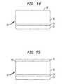
- FIG. 14is a schematic illustration of a substrate.
- FIG. 15is a schematic illustration of the substrate of FIG. 14 with a layer of photoresist.
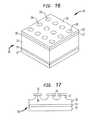
- FIG. 16is a perspective schematic illustration of the substrate of FIG. 14 with a layer of photoresist and a mask.
- FIG. 17is a schematic illustration of the substrate of FIG. 14 being etched.
- FIG. 18is a schematic illustration of the substrate of FIG. 14 with a second photoresist.
- FIG. 19is a schematic illustration of the substrate of FIG. 14 having the second photoresist developed.
- FIG. 20is a schematic illustration of the substrate of FIG. 14 being etched a second time.
- FIGS. 21A-21Dare example profiles of microcontacts.
- FIG. 21Eis an enlarged profile of the tip region of a microcontact shown in FIG. 21B .
- FIG. 22is a flowchart depicting a first embodiment.
- FIG. 23is a flowchart depicting a second embodiment.
- FIG. 24is a schematic illustration of a multi-layer substrate in application.
- FIG. 25is a schematic illustration of microelectronic unit.
- FIG. 26is a schematic illustration of two adjacent microelectronic units.
- FIG. 27is a schematic illustration of a microelectronic assembly.
- FIG. 28is another schematic illustration of a microelectronic assembly.
- FIG. 29is yet another schematic illustration of a microelectronic assembly.
- FIG. 30is a sectional view illustrating a completed microelectronic assembly in accordance with another embodiment.
- FIG. 31is a sectional view illustrating a completed microelectronic assembly in accordance with another embodiment.
- FIG. 32is a sectional view illustrating a completed microelectronic assembly in accordance with another embodiment.
- FIG. 33is a sectional view illustrating a completed microelectronic assembly in accordance with another embodiment.
- FIG. 34is a sectional view illustrating a completed microelectronic assembly in accordance with another embodiment.
- FIG. 35is a sectional view illustrating a completed microelectronic assembly in accordance with another embodiment.
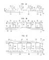
- the packaged microelectronic assembly 100includes a substrate 102 , a microelectronic element 104 in a face down or flip-chip position, and conductive columns 106 joining the substrate with the microelectronic element.
- the conductive columnsinclude conductive bumps or posts 108 which protrude above a face 105 of the substrate 102 that are aligned with conductive bumps or posts 110 protruding above a face 107 of the microelectronic element 104 .
- the conductive columns 106provide for increased height for chip-on-substrate packaging by increasing the standoff or vertical distance between the microelectronic element 104 and substrate 102 , while at the same time allowing for a decrease in the center-to-center horizontal distance or pitch P between conductive columns 106 .
- the ability to increase the distance between the substrate 102 and the microelectronic element 104may help reduce stress at the conductive columns, may help ease the application of underfill material 112 (see FIG. 2A ), and allow for a greater variety of underfills to be used.
- the substrate 102preferably includes a dielectric element 102 A.
- the dielectric element 102 Ahaving a top surface 101 and an oppositely facing bottom surface 103 .
- a plurality of conductive traces 109may extend along the top or bottom surfaces or both.
- the dielectric element 102 Amay be rigid or flexible.
- the dielectric element 102may be comprised of a polyimide or other polymeric sheet. Although the thickness of the dielectric element 102 may vary, the dielectric element 102 A most typically is up to 2 millimeters thick.
- the substrate 102may include other conductive elements such as external contacts (not shown) exposed at the bottom surface 103 .
- a conductive element “exposed at” a surface of a dielectric elementmay be flush with such surface; recessed relative to such surface; or protruding from such surface, so long as the conductive element is accessible for contact by a theoretical point moving towards the surface in a direction perpendicular to the surface.
- the traces and contactsmay be created using the methods illustrated in commonly assigned Published U.S. application Ser. No. 11/014,439, the disclosure of which is hereby incorporated by reference herein.
- the conductive elements(not shown) are disposed on the top surface 101 of substrate 102 .
- the conductive elementsmay also extend along the bottom surface 103 of substrate 102 ; on both the top and bottom surfaces 101 , 103 or within the interior of the substrate 102 .
- a statement that a first feature is disposed “on” a second featureshould not be understood as requiring that the first feature lie on a surface of the second feature.
- top surface and bottom surfaceare to be understood in relation to their placement relative to the microelectronic element, rather than in an gravitational frame of reference.
- a “top surface”shall mean a surface of the substrate adjacent to the front surface of the microelectronic element at which contacts, e.g., bond pads, metal posts, etc. are exposed.
- the “bottom surface”shall mean the surface of the substrate which is remote from the top surface.
- the bottom surfacetypically is a surface of the substrate on which contacts are exposed which can be joined with terminals of another element external to the packaged microelectronic element, such as a circuit panel.
- a “major surface” of a substrateshall mean a “top surface” of the substrate.
- Solid metal bumps or conductive posts 108also extend from the top surface 101 of the substrate 102 to form the first portion of the conductive columns 106 ( FIGS. 2 and 2A ).
- the conductive posts 108have top surfaces 111 and edge surfaces 113 extending at substantial angles away from the top surface of the substrate 102 such that a distinct angle is created where the edge surfaces 113 meet the top surfaces 101 of the substrate 102 .
- an angle greater than 90 degreesis created between the top surfaces 101 of the substrate 102 and the edge surfaces 113 of the conductive posts 108 . The angle will differ based upon the shape of the conductive post 108 .
- a cylindrical postmay have an angle of 90 degrees between the top surface 101 of the substrate 102 and the conductive post 108 .
- Exemplary processes and postsare described in Provisional Applications Nos. 60/875,730, filed on Dec. 19, 2006, and entitled Chip Capacitor Embedded PWB; 60/964,916, filed on Aug. 15, 2007, and entitled Multilayer Substrate with Interconnection Vias and Method of Manufacturing the Same; 60/964,823 filed on Aug. 15, 2007, and entitled Interconnection Element with Posts Formed by Plating; the disclosures all of which are incorporated herein by reference.
- the conductive posts 108may be formed by etching processes, as described in more detail herein.
- conductive posts 108may be formed by electroplating, in which posts 108 are formed by plating a metal onto a base metal layer through openings patterned in a dielectric layer such as a photoresist layer.
- the dimensions of the conductive posts 108can vary over a significant range, but most typically the height H 1 of each conductive post 108 extending from the top surface 103 of dielectric element 102 A is at least 50 microns and can extend up to 300 micrometers. These conductive posts 108 may have a height H 1 that is greater than its diameter or width W 1 . However, the height H 1 may also be smaller than the width W 1 , such as at least half the size of the width W 1 .
- the conductive posts 108may be made from any electrically conductive material, such as copper, copper alloys, gold and combinations thereof.
- the conductive posts 108may include at least an exposed metal layer that is wettable by solder.
- the postsmay be comprised of copper with a layer of gold at the surfaces of the posts.
- the conductive posts 108may include at least one layer of metal having a melting temperature that is greater than a melting temperature of the solder to which it will be joined.
- such conductive posts 108would include a layer of copper or be formed entirely of copper.
- the conductive posts 108may also take on many different shapes, including frustoconical.
- the base 114 and tip 116 of each of the conductive posts 108may be substantially circular or have a different shape, e.g. oblong.
- the bases 114 of the conductive posts 108typically are about 50-300 ⁇ m in diameter, whereas the tips 116 typically are about 25-200 ⁇ m in diameter.
- Each conductive post 108may have a base 114 adjacent the dielectric substrate 102 and a tip 116 remote from the dielectric substrate.
- the height H 1 of the conductive posts from the top surface 101 of the dielectric element 102 Atypically ranges from as little as 30 ⁇ m up to 200 ⁇ m.
- solder mask 118may be disposed over the substrate 102 and adjacent the conductive posts 108 .
- the solder mask 118helps to prevent solder overflow and bridging between adjacent columns 106 during the reflow phase.
- the microelectronic element 104has a front surface 122 and a rear surface 124 .
- the microelectronic element 104is preferably a semiconductor chip or the like prior to its packaging and interconnection with another element.
- the microelectronic elementis a bare die.
- conductive posts 110may be formed by etching processes.
- conductive posts 110may be formed by electroplating, in which posts 110 are formed by plating a metal onto a base metal layer through openings patterned in a photoresist layer.
- the posts 110 extending from the microelectronic element 104may have top surfaces 111 and edge surfaces 113 extending at substantial angles away from the top surface 122 of the microelectronic element such that a distinct angle is created between the microelectronic element and the conductive posts.
- an underbump metallization layer 120may be provided on the front surface 122 of the microelectronic element 104 .
- the underbump metallization layer 120is typically composed of a material including titanium, titanium-tungsten, chromium.
- the underbump metallization layer 120operates as the conducting metal contact for the conductive columns 106 .
- a passivation layer 119may also be provided on the front surface 122 of the microelectronic element 104 between the microelectronic element 104 and the underbump metallization layer 120 using known methods in the art.
- the dimensions of the conductive posts 110 extending from the microelectronic element 104may also vary over a significant range, but most typically the height H 2 of each conductive post 110 is not less than 50 microns.
- the conductive posts 110may have a height H 2 that is greater than its width W 2 . However, the height may also be smaller than the width W 2 , such as at least half the size of the width.
- the conductive posts 110are preferably made from copper or copper alloys, but may also include other electrically conductive materials, such as gold or combinations of gold and copper. Additionally, the conductive posts 110 may include at least one layer of metal having a melting temperature that is greater than a melting temperature of the solder to which it will be joined. For example, such conductive posts would include a layer of copper or be formed entirely of copper.
- the conductive posts 110can be cylindrical, so that the diameter of the bases 126 of the post and tips 128 of the posts are substantially equal. In one embodiment, the bases 126 and tips 128 of the conductive posts can be about 30-150 ⁇ m in diameter.
- Each conductive post 110may have a base 126 adjacent the substrate 102 and a tip 128 remote from the substrate 102 .
- the conductive posts 110may take on a variety of shapes, such as frustoconical, rectangular, or bar-shaped.
- a coating or cap of solder 130may be attached to the tips 128 of the conductive posts 110 or the portion of the conductive posts that are not attached to the microelectronic element 104 .
- the cap of solder 130can have the same diameter or width W 2 of the conductive posts 110 so that it becomes an extension of the conductive post 110 .
- the cap of solder 130can have a height H 3 ranging from approximately 25-80 ⁇ m.
- the height H 2 of the conductive posts 110 extending from the front surface 122 of the microelectronic element 104can be equal to the height H 1 of the conductive posts 108 extending from the top surface 101 of the dielectric element 102 A ( FIG. 1A ).
- the heightsmay alternatively differ, such that the height H 2 of the conductive posts 110 can be less than or greater than the height H 1 of the conductive posts 108 .
- the conductive posts 110 extending from the microelectronic element 104may have a height H 2 of 50 ⁇ m in length, whereas the conductive posts 108 extending from the substrate may have a height H 1 of 55 ⁇ m ( FIG. 2 ).
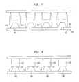
- the conductive posts 110 on the microelectronic element 104must be connected to the conductive posts 108 on the substrate 102 .
- the microelectronic element 104is inverted so that the conductive posts 110 of the microelectronic element 104 and the conductive posts 108 of the substrate 102 are aligned with one another and brought into close proximity.
- the cap of solder 130 on the microelectronic element 104is reflowed to allow the solder to wet the surfaces of the conductive posts 110 on the microelectronic element 104 and the conductive posts 108 on the substrate 102 . As shown in FIGS.
- the solderwill wet to the exposed surfaces of the conductive posts and create a conductive column 106 that extends from the microelectronic element to the substrate.
- the increased surface areas of the conductive columns 108 , 110 on the microelectronic element 104 and substrate 102 to which the solder is joinedcan help reduce the current density at the solder interface. Such decrease in current density may help reduce electromigration and provide for greater durability.
- the conductive columns 106include solder conductively interconnecting the conductive posts.
- the standoff or height H of the conductive columns extending between the base of the conductive post extending from the microelectronic element and the exposed portions of the base extending from the substrate in one exampleranges 80-100 ⁇ m.
- the walls 132 of the conductive columns 106can be convex or barrel shaped, wherein the midpoint region M of the conductive column (i.e., between the conductive posts 110 of the microelectronic element and conductive posts 108 of the substrate) has a width W that is greater than the widths W 1 , W 2 of the portions of the conductive columns 106 respectively adjacent the top surface 101 of the substrate 102 and front surface 102 of the microelectronic element 104 .
- contact pads 117may be formed on the microelectronic element 104 and substrate 102 using known methods.
- the lower post 108 that extends away from the substrate 102 , as well as the lower contact pad 117may be formed by separate etching steps, such as disclosed in International Application PCT No. WO 2008/076428, which published on Jun. 28, 2008 and the disclosure of which is incorporated herein by reference.
- a tri-metal substrate with top and bottom metal layers 123 and in intermediate etch stop layer or interior metal layer 121may be utilized to create the conductive post 108 and contact pad 117 .
- an exposed metal layer of a three-layer or more layered metal structureis etched in accordance with a photolithographically patterned photoresist layer to form the conductive post 108 , the etching process stopping on an interior metal layer 121 of the structure.
- the interior metal layer 121includes one or more metals different from that of the top and bottom metal layers 123 , the interior metal layer being of such composition that it is not attached by the etchant used to etch the top metal layer 123 .
- the top metal layer 123 from which the conductive posts 108 are etchedconsists essentially of copper
- the bottom metal layer 123may also consist essentially of copper
- the interior metal layer 121consists essentially of nickel.
- Nickelprovides good selectivity relative to copper to avoid the nickel layer from being attached with the metal layer is etched to form conductive posts 108 .
- another etching stepmay be conducted in accordance with another photolithographically patterned photoresist layer.
- the post 108may be further interconnected with other conductive features such as a via 115 , which is, in turn, further interconnected to other conductive features (not shown).
- the walls 232 of the conductive columns 106 ′may also be straight, such that the width W 5 is about equal to the widths W 4 , W 4 ′ of the conductive columns 106 ′ respectively adjacent the top surface 101 ′ of the substrate 102 ′ and front surface 122 ′ of the microelectronic element 104 ′. It should be appreciated that the widths W 4 , W 4 ′ do not need to be equal. Alternatively, the walls 232 ′ of the conductive columns 106 ′ may be concave (see FIG. 4 ), depending on the desired standoff to be achieved.
- the conductive columns 106 in accordance with the present inventionallow for a greater standoff height between the dielectric element and the microelectronic element while permitting a significant reduction in the pitch P (see FIGS. 1B , 2 ) between each of the conductive posts 110 exposed at the front surface 122 of the microelectronic element 104 , as well as the pitch P between each of the conductive posts 108 exposed at the top surface 101 of the substrate 102 .
- the pitch Pmay be as small as 50 ⁇ m or as large as 200 ⁇ m. It should be appreciated that by virtue of the fact that the conductive columns 108 , 110 are aligned with one another, the pitch P between each of the conductive posts 108 , 110 will be equal.
- the pitch Pmay also be a function of the diameter or width W 1 , W 2 of the conductive posts 108 , 110 , such that the diameter W 1 , W 2 of the base of the conductive posts is up to 75% of the pitch P.
- the ratio of the diameter W 1 , W 2 to the pitch Pcan be up to 3:4.
- the diameter W 1 , W 2 of the conductive posts 108 , 110may range up to 108 ⁇ m or 75% of the pitch P.
- the increased standoff heightreduces the strain on Low-k dielectric materials which can be present in the microelectronic element. Additionally, the increased standoff helps to minimize the problems typically associated with small pitches, such as electromigration and crowding. This is due to the fact that the conductive columns 106 are able to wet the surfaces of the conductive posts 108 , 110 .
- the solder cap 230can be placed at the tip 216 of the conductive post 208 extending from the substrate 202 .
- the width or diameter W 5 of the solder cap 230is roughly equal to the diameter W 6 of the base 214 of the conductive post 208 .
- the solder cap 230therefore extends beyond the tip 216 of the conductive post 208 extends from the substrate 202 .
- solder caps 330may be placed onto the conductive posts 310 , 308 extending from both the microelectronic element 304 and the substrate 302 .
- the conductive posts 308 , 310are placed in close proximity to one another. Heat is applied causing the solder caps 330 to reflow, wet, and fuse to the conductive posts 308 , 310 .
- the conductive column 306will preferably be similar to the conductive column 306 shown in FIG. 2 .
- FIG. 7an alternative arrangement for a microelectronic package is shown.
- the arrangementis similar to the one shown in FIG. 2 , the only difference being the absence of a solder mask adjacent the conductive posts extending from the substrate.
- vias 307can be used to conductively connect the conductive columns 406 to electronic circuitry (not shown) exposed at the bottom surface of the substrate 402 , as opposed to the top surface 401 of the substrate 402 .
- the use of vias 307obviates the need for the solder mask.
- a metal-to-metal bond between the conductive postsis made without the use of solder. Instead, a bond may be formed between the conductive posts 508 , 510 by deforming them into engagement with each other.
- the conductive posts 508 , 510are preferably formed from a malleable material with minimal resilience or spring-back as, for example, substantially pure gold.
- the conductive posts 508 , 510may be bonded together by eutectic bonding or anodic bonding between the posts and the material of the cover.
- the tips 516 , S 17 of the conductive posts 508 , 510may be coated with a small amount of tin, silicon, germanium or other material which forms a relatively low-melting alloy with gold, and the posts may be formed entirely from gold or have a gold coating on their surfaces.
- the conductive posts 508 , 510are engaged with one another and then heated, diffusion between the material of conductive posts 508 , 510 and the material on the tips 516 of the conductive posts forms an alloy having a melting point lower than the melting points of the individual elements at the interfaces between the posts and walls. With the assembly held at elevated temperature, further diffusion causes the alloying element to diffuse away from the interface, into the bulk of the gold of the posts, thereby raising the melting temperature of the material at the interface and causing the interface to freeze, forming a solid connection between the parts.
- the conductive posts 608 , 610are both preferably comprised of copper and are fused directly to one another without the presence of a low melting temperature metal such as a solder or tin between the conductive posts.
- a low melting temperature metalsuch as a solder or tin between the conductive posts.
- the joining surfaces of the conductive posts 608 , 610must be clean and substantially free of oxides, e.g., native oxides, before the conductive posts 608 , 610 are joined to the terminals.
- a process characterized as a surface treatment of etching or micro-etchingcan be performed to remove surface oxides of noble metals such as copper, nickel, aluminum, and others, the surface etching process being performed without substantially affecting the thicknesses of the bumps or metal layer which underlies them.
- This cleaning processis best performed only shortly before the actual joining process. Under conditions in which the component parts are maintained after cleaning in a normal humidity environment of between about 30 to 70 percent relative humidity, the cleaning process can usually be performed up to a few hours, e.g., six hours, before the joining process without affecting the strength of the bond to be achieved between the bumps and the capacitor terminals.
- a spacer structure 726is placed on the top surface 601 of the substrate 602 .
- the spacer structure 626can be formed of one or more materials such as polyimide, ceramic or one or more metals such as copper.
- the microelectronic element 604 from which conductive posts 610 extendare placed above the spacer structure 626 , such that the tips 628 of the conductive posts 610 of the microelectronic element 604 overlie the tips 616 of the conductive posts 608 of the substrate 602 . Referring to FIG.
- the spacer structure 626 , microelectronic element 604 and substrate 602are inserted between a pair of plates 640 and heat and pressure are simultaneously applied to the conductive posts in the directions indicated by arrows 636 .
- the pressure applied to plates 640has an effect of reducing the height of the conductive posts to a height H 6 lower than an original height H 5 of the conductive posts 608 , 610 as originally fabricated ( FIG. 10 ).
- An exemplary range of pressure applied to during this stepis between about 20 kg/cm2 and about 150 kg/cm2.
- the joining processis performed at a temperature which ranges between about 140 degrees centigrade and about 500 degrees centigrade, for example.
- the joining processcompresses the conductive posts 608 , 610 to an extent that metal from below the former top surfaces of the conductive posts 608 , 610 comes into contact and joins under heat and pressure. As a result of the joining process, the height of the conductive posts 608 , 610 may decrease by one micron or more.
- the joints between the conductive postsalso consist essentially of copper, thus forming continuous copper structures including the bumps and terminals.
- the plates and spacer structureare removed, leaving a subassembly 250 having conductive columns 606 formed from the conductive joinder of the conductive posts 608 , 610 .
- FIG. 12another alternative embodiment in accordance with the present invention is shown.
- a multilayer substratemay be used, such as the multilayer substrates described in U.S. appln. No. 60/964,823, filed on Aug. 15, 2007, and entitled Interconnection Element with Posts Formed by Plating; U.S. Appln. No. 60/964,916 filed Aug. 15, 2007, and entitled Multilayer Substrate With Interconnection Vias and Method of Manufacturing the Same; and U.S. patent application Ser. No. 11/824,484, filed on Jun. 29, 2007, and entitled Multilayer Wiring Element Having Pin Interface, the disclosures of which are incorporated herein.
- the multilayer substrate 702is joined in flip-chip manner with a microelectronic element 704 , e.g., a semiconductor chip having active devices, passive devices, or both active and passive devices thereon.
- a microelectronic element 704e.g., a semiconductor chip having active devices, passive devices, or both active and passive devices thereon.
- the tips 716 of the conductive posts 710which protrude from the top surface 701 of the multilayer substrate, are joined as described herein to conductive posts 710 extending from the microelectronic element.
- the conductive posts 708 of the multilayer substrate 702can be joined directly to the conductive posts 710 extending from the front surface microelectronic element, such as through a diffusion bond formed between a finished metal at the tips 160 of the posts, e.g., gold, and another metal present in the conductive pads and the posts.
- the conductive posts 708 , 710 postscan be joined together through a fusible metal such as a solder, tin or a eutectic composition, the fusible metal wetting the posts and the pads to form wetted or soldered joints.
- a fusible metalsuch as a solder, tin or a eutectic composition
- the fusible metalcan be provided in form of solder bumps (not shown), exposed at a front surface 722 of the microelectronic element 704 , the bumps being provided at the ends of either or both of the tips of the conductive posts.
- the conductive columnsmay also be utilized in stacked packaging, such as those packages described in commonly owned applications U.S. Appln. No. 60/963,209, filed Aug. 3, 2007, and entitled Die Stack Package Fabricated at the Wafer Level with Pad Extensions Applied To Reconstituted Wafer Elements; U.S. Appln. No. 60/964,069, filed Aug. 9, 2007, and entitled Wafer Level Stacked Packages with Individual Chip Selection; U.S. Appln. No. 60/962,200, filed Jul. 27, 2007, and entitled Reconstituted Wafer Stack Packaging with After-Applied Pad Extensions; and U.S. Appln. No. 60/936,617, filed Jun. 20, 2007, and entitled Reconstituted Wafer Level Stacking.
- a stacked package assemblyincludes a first subassembly 800 and a second subassembly 802 .
- the first and second subassembliesare virtually identical to the packaged microelectronic element shown in FIG. 2 , except for the fact that the substrates 806 , 806 ′ extend further out to accommodate conductive columns 808 extending between the substrates 806 , 806 ′ of the first and second subassemblies.
- the conductive columns 808also include a conductive post 812 extending from the substrate that connects to vias 814 extending through the top and bottom surfaces of the substrate on the second subassembly.
- FIG. 14is a schematic illustration of a tri-metal substrate 10 .
- the tri-metal substrate 10has a trace layer 12 , an etch stop layer 14 , a thick layer 16 , and a top surface 18 .
- the trace layer 12 and the thick layer 16may be formed of a readily etchable first metal such as copper, while the etch stop layer 14 may be formed of a metal, such as nickel, which is substantially resistant to etching by a process used to etch copper.
- the substrate 10may be formed of any suitable material as desired.
- FIG. 15is a schematic illustration of the tri-metal substrate 10 of FIG. 14 with a layer of a first photoresist 20 .
- the first photoresist 20is deposited onto the top surface 18 .
- the first photoresist 20may be any type of material that hardens or undergoes a chemical reaction when exposed to radiation such as light. Thus, any etch-resistant material maybe used. Positive and negative photoresists may also be utilized and are known in the art.
- FIG. 16is a perspective schematic illustration of the tri-metal substrate of FIG. 14 with the layer of first photoresist 20 and a mask 22 .
- the mask 22is often a transparent plate with opaque areas printed on it called a photomask or shadowmask, creating a pattern 24 on the mask 22 with areas covered by the mask 22 , denoted by reference numeral 26 , and areas not covered by the mask 22 , denoted by reference numeral 28 .
- the pattern 24 with the covered and uncovered areas, 26 and 28respectively, allows for selectively exposing parts of the first photoresist 20 to radiation.
- the mask 22is placed atop the first photoresist 20 , radiation is provided. Most often the radiation is in the form of ultraviolet light. This radiation exposes the first photoresist 20 at the uncovered areas 28 resulting in making the uncovered areas 28 insoluble. The opposite is true when a negative photoresist is used: the covered areas 26 become insoluble.
- the mask 22is removed.
- the first photoresist 20is then developed by washing with a solution which removes the first photoresist 20 in the locations where the first photoresist 20 has not become insoluble.
- the photoresist exposure and developmentleaves a pattern of insoluble material on the top of surface 18 of the substrate 10 . This pattern of insoluble material mirrors the pattern 24 of the mask 22 .
- the substrateis etched as shown in FIG. 17 .
- the etching processis interrupted. For example, the etching process can be terminated after a predetermined time.
- the etching processleaves first microcontact portions 32 projecting upwardly from substrate 10 at the thick layer 16 .
- the etchantattacks the thick layer 16 , it removes material beneath the edges of first photoresist 20 allowing the first photoresist 20 to project laterally from the top of first microcontact portions 32 , denoted as overhang 30 .
- the first photoresist 20remains at particular locations as determined by the mask 22 .
- a second layer of photoresist 34( FIG. 18 ) is deposited on the tri-metal substrate 10 .
- the second photoresist 34is deposited onto the thick layer 16 at the locations where the thick layer 16 has been previously etched.
- the second photoresist 34also covers the first microcontact portions 32 . If using electrophoretic photoresists, the second photoresist 34 , due to its inherent chemical properties, does not deposit onto the first photoresist 20 .
- the substrate with the first and second photoresists, 20 and 34is exposed to radiation and then the second photoresist is developed.
- the first photoresist 20projects laterally over portions of the thick layer 16 , denoted by overhang 30 .
- This overhang 30prevents the second photoresist 34 from being exposed to radiation and thus prevents it from being developed and removed, causing portions of the second photoresist 34 to adhere to the first microcontact portions 32 .
- the first photoresist 20acts as a mask to the second photoresist 34 .
- the second photoresist 34is developed by washing so as to remove the radiation exposed second photoresist 34 . This leaves the unexposed portions of second photoresist 34 on the first microcontact portions 32 .
- a second etching processis performed, removing additional portions of the thick layer 16 of the tri-metal substrate 10 , thereby forming second microcontact portions 36 below the first microcontact portions 32 as shown in FIG. 20 .
- the second photoresist 34still adhered to first microcontact portions 32 , protects the first microcontact portions 32 from being etched again.
- stepsmay be repeated as many times as desired to create the preferred aspect ratio and pitch forming third, fourth or nth microcontact portions.
- the processmay be stopped when the etch-stop layer 14 is reached.
- the first and second photoresists 20 and 34may be stripped entirely.
- the slope or dX/dZmay change abruptly at the boundary 52 between the first and second portions. Within each portion, the slope or dX/dZ typically does not change abruptly with position in the Z direction and thus, does not define a step change. Within each portion, typically the slope or dX/dZ changes at most gradually with position in the Z direction.
- the circumferential surface 44 of the first portion 32 of the microcontact region and the circumferential surface 46 of the second portion 38are concave surfaces, and each has a slope or dX/dZ which changes at most gradually with position in the Z direction.
- concavemeans that at every height between the boundaries of the circumferential surfaces (e.g., at every height 29 between an upper boundary 19 of the circumferential surface 44 and a lower boundary 52 of that circumferential surface 44 (FIG.
- the circumferential surfaceencloses a smaller diameter 25 than the diameter, at the same height 29 , enclosed by a theoretical conical surface defined by a series of straight lines extending between the boundaries. For example, every point on circumferential surface 44 between boundaries 19 , 52 lies inward from the theoretical conical surface 48 defined by a series of straight lines extending through the boundaries 19 , 52 .
- the particular functions and hence the shape of the microcontactsare determined by the etching conditions used in the first and second etching steps.
- the composition of the etchant and etching temperaturecan be varied to vary the rate at which the etchant attacks the metal layer.
- the mechanics of contacting the etchant with the metal layercan be varied.
- the etchantcan be sprayed forcibly toward the substrate, or the substrate can be dipped into the etchant.
- the etching conditionsmay be the same or different during etching of the first and second portions.
- the circumferential surfaces 44 , 46 of each of the first and second portions 32 , 36are concave.
- the first portion 32has a circumferential surface 44 which flares outwardly in the downward direction, so that the magnitude of the slope or dX/dZ increases in the downward direction.
- the second portion 36also has a circumferential surface 46 flares outwardly; the magnitude of the slope or dX/dZ of the second is at a minimum at boundary 52 , and progressively increases in the direction toward the base of the post. There is a substantial change in slope at boundary 52 .
- the maximum width or diameter X of the second portion, at the base of the microcontact where the microcontact joins layer 14is substantial greater than the maximum width or diameter of the first portion.
- FIG. 21Dillustrates a profile of a microcontact 38 having more than two portions. This type of profile may result in the event the steps of the processes described herein are performed numerous times.
- this particular microcontact 38has four portions, the first and second portions 32 and 36 , respectively, and third and fourth portions, 40 and 42 , respectively. These four portions may have any dimension and be wider or slimmer than another portion as desired. In this instance, there may be greater than one boundary.
- FIGS. 21A-21Dare only representative profiles and a variety of profiles may be achieved.
- the first portion 32can also be referred to as the tip region
- the fourth portion 42can also be referred to as the base region
- the second portion 36 and the third portion 40can be referred to as intermediate regions.
- the entire first photoresist 20may be removed.
- the second photoresist 34may be deposited over the entire surface of the substrate 10 .
- the mask 22is placed onto the second photoresist 34 .
- the mask 22must be properly aligned so as to expose only at the locations previously exposed, on the first microcontact portions 32 .
- the second photoresist 34is then developed and further etching may be performed on the substrate 10 .
- FIG. 22is a flowchart depicting the first embodiment. Beginning at step 1100 , a substrate is provided. Then at step 1102 , a photoresist n is deposited onto the substrate. Then at step 1104 , a mask is placed atop the photoresist n. At step 1106 the photoresist n is exposed to radiation. Subsequently, at step 1108 the mask is removed and then at step 1110 , the photoresist n is developed at select locations and the substrate is etched.
- FIG. 23is a flowchart depicting a second embodiment. Steps 1200 - 1210 of the second embodiment mirror steps 1100 - 1110 of the first embodiment. However, at step 1212 , the entire photoresist n is removed. Then, at step 1214 , another layer of photoresist n+1 is deposited onto the substrate. Next, the mask is placed back onto the substrate at step 1216 . During this step, the mask must be aligned such that its pattern is situated in substantially the same location as when the mask was placed on the photoresist n. Subsequently, at step 1218 , the photoresist n+1 is exposed to radiation and the mask is removed.
- the etch-stop layer 14 and the thin layer 12may be united with a dielectric layer and then thin layer 12 may be etched to form traces so as to provide a component with the microcontacts connected to the traces and with the microcontacts projecting from the dielectric layer.
- Such a structurecan be used, for example, as an element of a semiconductor chip package.
- U.S. patent application Ser. No. 11/318,822, filed Dec. 27, 2005, the disclosure of which is hereby incorporated by reference herein,may be used.
- the structure described hereinmay be an integral part of a multilayer substrate 10 , for instance, the top layer of a multilayer substrate 10 , as shown in FIG. 24 .
- Microcontacts 38may be soldered to the die 54 .
- the solder 56may wick around a portion of the microcontacts 38 . Wicking provides very good contact between the microcontacts 38 and the die 54 .
- Other bonding processes besides solder 56may also be used.
- Surrounding the microcontacts 38is underfill 58 , used to adhere the die 54 to the microcontacts 38 and the substrate 10 . Any type of underfill 58 may be used as desired or underfill 58 may be omitted.
- Below the microcontacts 38are traces 60 and a dielectric layer 62 . Terminals 64 are disposed at the bottom of the substrate 10 .
- the etch-resistant metalmay be left in place on the tip of the microcontact.
- a maskmay be used to limit deposition of the second etch-resistant metal to only the first portions 32 of the microcontacts, so that the areas between the microcontacts remain free of the etch-resistant metal.
- the entire first layer of etch-resistant metalmay be removed upon etching first microcontact portions 32 , then a second layer of etch-resistant metal may be deposited to protect the first microcontact portions 32 .
- a microelectronic unit 70having microcontacts 72 .
- the microcontacts 72have an etch stop layer 74 .
- the microcontacts 72project vertically from a metallic layer that has been formed into traces 76 . There may be gaps or spaces 78 between the traces 76 .
- a first layer of dielectric 80may be adhered to a bottom side of the unit 70 adjacent the traces 76 . Openings 82 in the first layer of dielectric 80 allow the traces 76 to form electronic contacts.
- a second layer of a dielectric 84may be formed on a top side of the unit 70 .
- the microcontacts formed from these processesmay have a typical height ranging from about 40 microns to about 200 microns. Further, the typical pitch between microcontacts may be less than about 200 microns, preferably less than 150 microns.
- two microcontactsare shown having a tip diameter d and a microcontact height h.
- a pitch Pis defined by the distance between the longitudinal axes of the two microcontacts.
- the adhesion between the tips of the pins and spots of photoresist used to protect the tips during etchingis proportional to the area of the tips, and hence to the square of the tip diameter. Therefore, with very small tip diameters, the photoresist spots can be dislodged during processing. Thus, using conventional processes, it has been difficult to form microcontacts with very small pitch.
- P ⁇ Pothe pitch between microcontacts using the process recited herein
- the process described herein, with at least two etchescan achieve a pitch P of about 80 microns or less.
- the multi-step etching processallows formation of unitary metallic microcontacts or posts from a single metallic layer with combinations of pitch, tip diameter and height not attainable in conventional etching processes. As the number of etching steps increases, the minimum attainable pitch for a given tip diameter and height decreases.
- the chip carrierincludes a first dielectric layer 62 which may be formed from a material such as polyimide, BT resin or other dielectric material of the type commonly used for chip carriers.
- the chip carrieralso includes traces 60 connected to some or all of the microcontacts 38 .
- the tracesincorporate terminals 61 .
- the microcontacts 38project from a first side of dielectric layer 62 , facing upwardly as seen in FIG. 27 .
- Dielectric layer 62has openings 82 , and terminals 61 are exposed at the second or downwardly facing surface of the first dielectric layer 62 through openings 82 .
- the carrierfurther includes an optional second dielectric layer 84 .
- the tips of microcontacts 38are bonded to contacts 55 of a microelectronic element such as a semiconductor chip or die 54 .
- the tips of the microcontactsmay be solder-bonded to the contacts 55 of the microelectronic element.
- Other bonding processessuch as eutectic bonding or diffusion bonding, may be employed.
- the resulting packaged microelectronic elementhas some or all of contacts 55 on the microelectronic element connected to terminals 61 by the microcontacts and traces.
- the packaged microelectronic elementmay be mounted to a circuit panel 92 , such as a printed circuit board by bonding terminals 61 to pads 94 on the circuit board.
- pads 94 on the circuit panel 92may be soldered to the terminals 61 , at openings 82 , using solder balls 96 .
- the structure of the chip carriercan be varied.
- the chip carriermay include only one dielectric layer.
- the tracesmay be disposed on either side of the dielectric layer.
- the chip carriermay include a multi-layer dielectric, and may include multiple layers of traces, as well as other features such as electrically conductive ground planes.
- a process for further embodiment of the inventionuses a structure having post portions 1550 ( FIG. 28 ) projecting from a surface 1526 such as a surface of dielectric layer 1510 .
- Post portions 1550may be formed by any process, but desirably are formed by an etching process similar to those discussed above.
- a metallic or other conductive layer 1502is applied over the tips 1533 of post portions 1550 .
- layer 1502may be laminated on the structure incorporating portions 1550 , and metallurgically bonded to the tips of post portions 1550 .
- Layer 1502is selectively treated so as to remove material of the layer remote from post portions 1550 , but leave at least part of the layer thickness overlying post portions 1550 , and thereby form additional post portions 1504 ( FIG. 29 ) aligned with post portions 1550 , and thus form composite microcontacts, each including a proximal post portion 1550 close to the substrate and a distal post portion 1504 remote from the substrate, the distal portion projecting in the vertical or z direction from the proximal portion.
- the treatment applied to layer 1502may include an etching process as discussed above, using spots of an etch-resistant material 1506 aligned with post portions 1550 .
- a protective layer such as a dielectric encapsulant 1508may be applied to cover post portions 1550 before etching layer 1502 .
- post portions 1550may be plated or otherwise covered with an etch-resistant conductive material such as nickel or gold before etching layer 1502 .
- the process of building up successive post portionsmay be repeated so as to form additional portions on portions 1504 , so that microcontacts of essentially any length can be formed.
- the long microcontactsprovide increased flexibility and movement of the post tips.
- the encapsulantdesirably is compliant so that it does not substantially limit flexure of the posts. In other embodiments, the encapsulant is removed before the components are used.
- the microcontactsare illustrated in conjunction with a dielectric substrate 1522 and traces 1528 similar to those discussed above, this process can be used to fabricate microcontacts on essentially any structure.
- each microcontacthas a horizontal or width dimension x which varies over the vertical or z-direction extent of the proximal post portion 1550 and which increases abruptly, in substantially stepwise fashion, at the juncture between the proximal post portion 1550 and the distal portion 1504 , and varies along the vertical extent of the distal portion.
- the slope of the variation in width with vertical locationalso changes abruptly at the juncture between the post portions.
- the pattern of variation of the horizontal or width dimension within each post portiondepends upon the process used for etching or otherwise forming such post portion.
- the distal post portions 1504may be formed by a multi-stage etching process as discussed above, so that each distal post portion includes different sub-portions with different functions defining the variation of width x in the vertical or z direction.
- FIG. 30illustrates a cross-sectional view of a packaged microelectronic assembly 900 in accordance with a variation of the assembly shown and described above with respect to FIGS. 1A-2A , in which posts 916 extending from a front surface of the microelectronic element 902 include multiple-etched conductive posts.
- the packaged microelectronic assembly 900includes a substrate 901 such as that shown and described above with respect to FIG. 1A .
- the assemblyalso includes a microelectronic element 902 in a face down or flip-chip position and conductive columns 903 joining the substrate with the microelectronic element.
- the conductive columns 903include conductive bumps or posts 912 that protrude above a top surface 906 of the substrate 901 that are aligned with conductive bumps or posts 916 protruding above a front surface 909 of the microelectronic element 902 .
- the microelectronic element 902has a front surface 909 .
- the microelectronic element 902preferably is a semiconductor chip or the like.
- the microelectronic elementmay be a bare die.
- the posts 916may extend from bond pads 908 exposed at the front surface 909 of the microelectronic element 902 .
- the conductive columns 903include solder conductively interconnecting the conductive posts 912 and 916 , thereby creating the conductive columns 903 that extend from the microelectronic element 902 to the substrate 901 .
- the conductive columns 903may be bonded together by any process, material, or combination of materials disclosed herein with reference to other embodiments.
- the conductive columns 903may be bonded together by eutectic bonding or anodic bonding between the posts and the material of the cover.
- the posts 912may be any type of conductive posts, including any type of conductive posts disclosed herein with reference to other embodiments.
- the posts 912may have any shape, including frustoconical.
- the base and tip of each of the conductive posts 912may be substantially circular or have a different shape, e.g., oblong.
- the posts 912 extending from the substrate 901may be the posts 108 shown in FIGS. 1A , 1 C, 2 , and 2 A, such that the posts 916 extending from the microelectronic element 902 may replace the corresponding posts 110 , each of which may include a cap of solder 130 .
- the posts 912may be the posts 208 shown in FIG. 5 and each including a cap of solder 230 , such that the posts 916 may replace the corresponding posts 210 .
- the posts 912may be the posts 308 shown in FIG. 6 and each including a cap of solder 330 , such that the posts 916 may replace the corresponding posts 310 , each of which may also include a cap of solder 330 .
- the posts 912may be the posts 508 shown in FIG. 8 , such that the posts 916 may replace the corresponding posts 510 .
- the posts 912 and 916preferably are made from a malleable material with minimal resistance or spring-back as, for example, substantially pure gold, and each post is configured to be deformed into engagement with a corresponding post without the use of solder.
- the posts 912may be the posts 708 of the multilayer substrate 702 shown in FIG. 12 , such that the posts 916 may replace the corresponding posts 710 .
- the posts 912can be joined directly to the posts 916 extending from the microelectric element 902 , such as through a diffusion bond formed between a finished metal at the tips of the posts, e.g., gold, and another metal present in the conductive pads and the posts.
- the posts 912 and 916can be joined together through a fusible metal such as a solder, tin or a eutectic composition, the fusible metal wetting the posts and the pads to form wetted or soldered joints.
- the posts 912may be the posts 812 and the other posts extending from the substrates 806 , 806 ′ shown in FIG. 13 , such that the posts 916 may replace the corresponding posts 810 , 810 ′.
- the posts 912 and 916may be used in a stacked package assembly such as the assemblies 800 , 800 ′ shown in FIG. 13 .
- the posts 912 and 916may be used with a multilayer substrate, such as the multilayer substrate 10 shown in FIG. 24 .
- the posts 912may be the microcontacts 38 shown in FIG. 24
- the posts 916may extend from a microelectronic element or other component such as the die 54 , such that the posts 912 may be bonded to the posts 916 using solder or other post bonding processes described herein.
- the posts 912may be the microcontacts 72 shown in FIG. 25 , where the posts 912 project vertically from a metallic layer that has been formed into traces 76 .
- the posts 912may be the microcontacts 38 shown in FIG. 27 , where the posts 912 extend from a substrate that includes traces 60 , openings 82 , terminals 61 , and an optional second dielectric layer 84 .
- the posts 916are multiple-etched conductive posts. As shown in FIG. 30 , the posts 916 are the same as the dual-etched microcontacts 38 shown in FIG. 21B . As described above with reference to FIG. 21B , each post 916 will be generally in the form of a body of revolution about a central axis extending in a vertical or Z direction, downwardly from the microelectronic element 902 and generally perpendicular to the plane of the front surface 909 .
- the posts 916may be any multiple-etched conductive posts, including for example, the multiple-etched microcontacts 38 shown in FIGS. 21A , 21 C, and 21 D. Although the posts 916 are shown as being dual-etched in FIG. 30 , the posts 916 may undergo more than two etchings, such as four etchings as shown in FIG. 21D .
- the posts 916may be composite microcontacts having the structure shown in FIGS. 28 and 29 , in which each post 916 includes a proximal post portion 1550 close to the microelectronic element 902 and a distal post portion 1504 remote from the microelectronic element.
- FIG. 31illustrates a cross-sectional view of a packaged microelectronic assembly 920 in accordance with a variation of the assembly shown and described above with respect to FIGS. 1A-2A , in which posts 932 extending from a top surface of the substrate 921 include multiple-etched conductive posts.
- Packaged microelectronic assembly 920 shown in FIG. 31is substantially the same as packaged microelectronic assembly 900 shown in FIG. 30 , except that the posts 932 extending from the substrate 921 are multiple-etched conductive posts, such as the dual-etched microcontacts 38 shown in FIG. 21B , while the posts 936 extending from the microelectronic element 922 may be any type of conductive posts, including any type of conductive posts disclosed herein with reference to other embodiments.
- the packaged microelectronic assembly 920includes a substrate 921 such as that shown and described above with respect to FIG. 1A .
- the assemblyalso includes a microelectronic element 922 in a face down or flip-chip position, and conductive columns 923 joining the substrate with the microelectronic element.
- the conductive columns 923include conductive bumps or posts 932 that protrude above a top surface 926 of the substrate 921 that are aligned with conductive bumps or posts 936 protruding above a front surface 929 of the microelectronic element 922 .
- the conductive columns 923include solder conductively interconnecting the conductive posts 932 and 936 , thereby creating the conductive columns 923 that extend from the microelectronic element 922 to the substrate 921 .
- the conductive columns 923may be bonded together by any process, material, or combination of materials disclosed herein with reference to other embodiments.
- the posts 932are multiple-etched conductive posts. As shown in FIG. 31 , the posts 932 are the same as the dual-etched microcontacts 38 shown in FIG. 21B . In other embodiments (not shown), the posts 932 may be any multiple-etched conductive posts, including for example, the multiple-etched microcontacts 38 shown in FIGS. 21A , 21 C, and 21 D. Although the posts 932 are shown as being dual-etched in FIG. 31 , the posts 932 may undergo more than two etchings, such as four etchings as shown in FIG. 21D .
- the posts 932may be composite microcontacts having the structure shown in FIGS. 28 and 29 , in which each post 932 includes a proximal post portion 1550 close to the substrate 922 and a distal post portion 1504 remote from the substrate.
- the posts 936may be any type of conductive posts, including any type of conductive posts disclosed herein with reference to other embodiments.
- the posts 936may have any shape, including frustoconical.
- the base and tip of each of the conductive posts 936may be substantially circular or have a different shape, e.g., oblong.
- the posts 936 extending from the microelectronic element 922may be the posts 110 shown in FIGS. 1B , 2 , and 2 A, such that the posts 932 extending from the substrate 921 may replace the corresponding posts 108 .
- Each of the posts 936may include a cap of solder 130 .
- the posts 936may be the posts 210 shown in FIG. 5 , such that the posts 932 may replace the corresponding posts 208 that include a cap of solder 230 .
- the posts 936may be the posts 310 shown in FIG. 6 and each including a cap of solder 330 , such that the posts 932 may replace the corresponding posts 308 , each of which may also include a cap of solder 330 .
- the posts 936may be the posts 510 shown in FIG. 8 , such that the posts 932 may replace the corresponding posts 508 .
- the posts 932 and 936preferably are made from a malleable material with minimal resistance or spring-back as, for example, substantially pure gold, and each post is configured to be deformed into engagement with a corresponding post without the use of solder.
- the posts 936may be the posts 610 shown in FIGS. 9-11 , such that the posts 932 may replace the corresponding posts 608 .
- the posts 932 and 936preferably are comprised of copper, and each post is configured to be fused directly to a corresponding post without the presence of a low melting temperature metal such as a solder or tin between the conductive posts.
- the posts 936may be the posts 810 , 810 ′ shown in FIG. 13 , such that the posts 932 may replace the corresponding posts extending from the substrates 806 , 806 ′.
- the posts 932 and 936may be used in a stacked package assembly such as the assemblies 800 , 800 ′ shown in FIG. 13 .
- the posts 932 and 936may be used with a multilayer substrate, such as the multilayer substrate 10 shown in FIG. 24 .
- the posts 932may be the microcontacts 38 shown in FIG. 24
- the posts 936may extend from a microelectronic element or other component such as the die 54 , such that the posts 932 may be bonded to the posts 936 using solder or other post bonding processes described herein.
- FIG. 32illustrates a cross-sectional view of a packaged microelectronic assembly 940 in accordance with a variation of the assembly shown and described above with respect to FIGS. 1A-2A , in which posts 952 extending from a top surface of the substrate 941 and posts 956 extending from a front surface of the microelectronic element 942 include multiple-etched conductive posts.
- Packaged microelectronic assembly 940 shown in FIG. 32is substantially the same as packaged microelectronic assembly 900 shown in FIG. 30 and packaged microelectronic assembly 920 shown in FIG. 31 , except that both the posts 952 extending from the substrate 941 and the posts 956 extending from the microelectronic element 942 are multiple-etched conductive posts, such as the dual-etched microcontacts 38 shown in FIG. 21B .
- the packaged microelectronic assembly 940includes a substrate 941 such as that shown and described above with respect to FIG. 1A .
- the assemblyalso includes a microelectronic element 942 in a face down or flip-chip position, and conductive columns 943 joining the substrate with the microelectronic element.
- the conductive columns 943include conductive bumps or posts 952 that protrude above a top surface 946 of the substrate 941 that are aligned with conductive bumps or posts 956 protruding above a front surface 949 of the microelectronic element 942 .
- the conductive columns 943include solder conductively interconnecting the conductive posts 952 and 956 , thereby creating the conductive columns 943 that extend from the microelectronic element 942 to the substrate 941 .
- the conductive columns 943may be bonded together by any process, material, or combination of materials disclosed herein with reference to other embodiments.
- the posts 952 and 956are multiple-etched conductive posts. As shown in FIG. 32 , the posts 952 and 956 are the same as the dual-etched microcontacts 38 shown in FIG. 21B . In other embodiments (not shown), the posts 952 and 956 may be any multiple-etched conductive posts, including for example, the multiple-etched microcontacts 38 shown in FIGS. 21A , 21 C, and 21 D.
- the posts 952 and 956are shown as the same as the dual-etched microcontacts 38 shown in FIG. 21B , in other embodiments (not shown), the posts 952 may have a different multiple-etched shape than the posts 956 , including for example, where the posts 952 are shaped as shown in FIG. 21A and the posts 956 are shaped as shown in FIG. 21C , such that first and second functions that determine the shape of the posts 952 and that are determined by the etching conditions used in the first and second etching steps of the posts 952 may be different than third and fourth functions that determine the shape of the posts 956 and that are determined by the etching conditions used in the first and second etching steps of the posts 956 .
- each post 952 and 956may undergo more than two etchings, such as four etchings as shown in FIG. 21D .
- the posts 952 and 956may be composite microcontacts having the structure shown in FIGS. 28 and 29 , in which each post 952 and 956 includes a proximal post portion 1550 close to the substrate 942 and a distal post portion 1504 remote from the substrate.
- either or both of the posts 952 and 956may include a cap of solder, as shown in FIGS. 1B , 1 C, 5 , and 6 .
- the posts 952 and 956may be made from a malleable material with minimal resistance or spring-back as, for example, substantially pure gold, and each post is configured to be deformed into engagement with a corresponding post without the use of solder.
- the posts 952 and 956may be comprised of copper, and each post may be configured to be fused directly to a corresponding post without the presence of a low melting temperature metal such as a solder or tin between the conductive posts.
- the posts 952 and 956may be used in a stacked package assembly such as the assemblies 800 , 800 ′ shown in FIG. 13 .
- the posts 952 and 956may be used with a multilayer substrate, such as the multilayer substrate 10 shown in FIG. 24 .
- FIG. 33illustrates a cross-sectional view of a packaged microelectronic assembly 960 in accordance with a variation of the assembly shown and described above with respect to FIGS. 1A-2A , in which posts 972 extending from a top surface of the substrate 961 include multiple-etched conductive posts.
- Packaged microelectronic assembly 960 shown in FIG. 33is substantially the same as packaged microelectronic assembly 920 shown in FIG. 31 , except that the posts 976 extending from the microelectronic element 962 have a frustoconical shape, such as any of the frustoconical posts or microcontacts disclosed herein with reference to other embodiments.
- the packaged microelectronic assembly 960includes a substrate 961 such as that shown and described above with respect to FIG. 1A .
- the assemblyalso includes a microelectronic element 962 in a face down or flip-chip position, and conductive columns 963 joining the substrate with the microelectronic element.
- the conductive columns 963include conductive bumps or posts 972 that protrude above a top surface 966 of the substrate 961 that are aligned with conductive bumps or posts 976 protruding above a front surface 969 of the microelectronic element 962 .
- the conductive columns 963include solder conductively interconnecting the conductive posts 972 and 976 , thereby creating the conductive columns 963 that extend from the microelectronic element 962 to the substrate 961 .
- the conductive columns 963may be bonded together by any process, material, or combination of materials disclosed herein with reference to other embodiments.
- the posts 972are multiple-etched conductive posts. As shown in FIG. 33 , the posts 972 are the same as the dual-etched microcontacts 38 shown in FIG. 21B . In other embodiments (not shown), the posts 972 may be any multiple-etched conductive posts, including for example, the multiple-etched microcontacts 38 shown in FIGS. 21A , 21 C, and 21 D. Although the posts 972 are shown as being dual-etched in FIG. 33 , the posts 972 may undergo more than two etchings, such as four etchings as shown in FIG. 21D .
- the posts 972may be composite microcontacts having the structure shown in FIGS. 28 and 29 , in which each post 972 includes a proximal post portion 1550 close to the substrate 962 and a distal post portion 1504 remote from the substrate.
- either or both of the posts 972 and 976may include a cap of solder, as shown in FIGS. 1B , 1 C, 5 , and 6 .
- the posts 972 and 976may be made from a malleable material with minimal resistance or spring-back as, for example, substantially pure gold, and each post is configured to be deformed into engagement with a corresponding post without the use of solder.
- the posts 972 and 976may be comprised of copper, and each post may be configured to be fused directly to a corresponding post without the presence of a low melting temperature metal such as a solder or tin between the conductive posts.
- the posts 972 and 976may be used in a stacked package assembly such as the assemblies 800 , 800 ′ shown in FIG. 13 .
- the posts 972 and 976may be used with a multilayer substrate, such as the multilayer substrate 10 shown in FIG. 24 .
- FIG. 34illustrates a cross-sectional view of a packaged microelectronic assembly 980 in accordance with a variation of the assembly shown and described above with respect to FIGS. 1A-2A , in which posts 996 extending from a front surface of the microelectronic element 982 include multiple-etched conductive posts.
- Packaged microelectronic assembly 980 shown in FIG. 33is substantially the same as packaged microelectronic assembly 900 shown in FIG. 30 , except that the posts 912 extending from the substrate 901 in FIG. 30 have been replaced with bond pads 992 attached to the substrate 981 , such as any of the bond pads disclosed herein with reference to other embodiments.
- the packaged microelectronic assembly 980includes a substrate 981 such as that shown and described above with respect to FIG. 1A .
- the assemblyalso includes a microelectronic element 982 in a face down or flip-chip position, and conductive columns 983 joining the substrate with the microelectronic element.
- the conductive columns 983include conductive bond pads 992 that are attached to a top surface 986 of the substrate 981 that are aligned with conductive bumps or posts 996 protruding above a front surface 989 of the microelectronic element 982 .
- the conductive columns 983include solder conductively interconnecting the conductive posts 996 and pads 992 , thereby creating the conductive columns 983 that extend from the microelectronic element 982 to the substrate 981 .
- the conductive columns 983may be bonded together by any process, material, or combination of materials disclosed herein with reference to other embodiments.
- the posts 996are multiple-etched conductive posts. As shown in FIG. 34 , the posts 996 are the same as the dual-etched microcontacts 38 shown in FIG. 21B . In other embodiments (not shown), the posts 996 may be any multiple-etched conductive posts, including for example, the multiple-etched microcontacts 38 shown in FIGS. 21A , 21 C, and 21 D. Although the posts 996 are shown as being dual-etched in FIG. 33 , the posts 996 may undergo more than two etchings, such as four etchings as shown in FIG. 21D .
- the posts 996may be composite microcontacts having the structure shown in FIGS. 28 and 29 , in which each posts 996 includes a proximal post portion 1550 close to the microelectronic element 981 and a distal post portion 1504 remote from the microelectronic element.
- either or both of the pads 992 and posts 996may include a cap of solder, as shown in FIGS. 1B , 1 C, 5 , and 6 .
- the pads 992 and posts 996may be made from a malleable material with minimal resistance or spring-back as, for example, substantially pure gold, and each post is configured to be deformed into engagement with a corresponding post without the use of solder.
- the pads 992 and posts 996may be comprised of copper, and each post may be configured to be fused directly to a corresponding post without the presence of a low melting temperature metal such as a solder or tin between the conductive posts.
- the pads 992 and posts 996may be used in a stacked package assembly such as the assemblies 800 , 800 ′ shown in FIG. 13 .
- the pads 992 and posts 996may be used with a multilayer substrate, such as the multilayer substrate 10 shown in FIG. 24 .
- FIG. 35illustrates a cross-sectional view of a packaged microelectronic assembly 1000 in accordance with a variation of the assembly shown and described above with respect to FIGS. 1A-2A , in which posts 1012 extending from a top surface of the substrate 1001 and posts 1016 extending from a front surface of the microelectronic element 1002 include multiple-etched conductive posts.
- Packaged microelectronic assembly 1000 shown in FIG. 35is substantially the same as packaged microelectronic assembly 940 shown in FIG. 32 , except that the solder included in the conductive columns 1003 that conductively interconnect the conductive posts 1012 and 1016 does not touch the conductive pads 1008 of the microelectronic element 1002 .
- the solder included in the conductive columns 1003does not touch the surface 1006 of the substrate 1001 or does not touch the pads (not shown) from which posts 1012 of the substrate can extend, such pads which may be exposed at a surface 1006 of the substrate.
- the conductive columns 903 , 923 , 943 , 963 , and 983 shown in FIGS. 30-34provide for increased height for chip-on-substrate packaging by increasing the standoff or vertical distance between the microelectronic element and the substrate, while at the same time allowing for a decrease in the center-to-center horizontal distance or pitch between the conductive columns.
- the ability to increase the distance between the substrate and the microelectronic elementmay help reduce stress at the conductive columns, may help ease the application of underfill (see, for example, FIG. 2A ), and allow for a greater variety of underfills to be used.
- the posts 912 and 916 shown in FIG. 30 , the posts 932 and 936 shown in FIG. 31 , the posts 952 and 956 shown in FIG. 32 , the posts 972 and 976 shown in FIG. 33 , and the bond pads 992 and the posts 996 shown in FIG. 34may be made from any electrically conductive material, such as copper, copper alloys, gold and combinations thereof.
- the posts 932 and 936 shown in FIG. 31 , the posts 952 and 956 shown in FIG. 32 , the posts 972 and 976 shown in FIG. 33 , and the bond pads 992 and the posts 996 shown in FIG. 34may include an exposed metal layer that is wettable by solder.
- the postsmay be comprised of copper with a layer of gold at the surfaces of the posts.
- the posts 932 and 936 shown in FIG. 31 , the posts 952 and 956 shown in FIG. 32 , the posts 972 and 976 shown in FIG. 33 , and the bond pads 992 and the posts 996 shown in FIG. 34may include at least one layer of metal having a melting temperature that is greater than a melting temperature of the solder to which it will be joined.
- such conductive postswould include a layer of copper or be formed entirely of copper.
- each post extending from the front surfaces of the substrate and the microelectronic elementis at least 30 microns and can extend up to 300 microns.
- These postsmay have a height (approximately perpendicular to the front surfaces of the substrate and the microelectronic element, respectively) that is greater than its diameter or width (approximately parallel to the front surfaces of the substrate and the microelectronic element, respectively).
- the heightmay also be smaller than the width, such as at least half the size of the width.
Landscapes
- Engineering & Computer Science (AREA)
- Computer Hardware Design (AREA)
- Microelectronics & Electronic Packaging (AREA)
- Power Engineering (AREA)
- Physics & Mathematics (AREA)
- Condensed Matter Physics & Semiconductors (AREA)
- General Physics & Mathematics (AREA)
- Manufacturing & Machinery (AREA)
- Ceramic Engineering (AREA)
- Wire Bonding (AREA)
- Internal Circuitry In Semiconductor Integrated Circuit Devices (AREA)
- Fuses (AREA)
Abstract
Description
Claims (47)
Priority Applications (9)
| Application Number | Priority Date | Filing Date | Title |
|---|---|---|---|
| US12/832,376US8330272B2 (en) | 2010-07-08 | 2010-07-08 | Microelectronic packages with dual or multiple-etched flip-chip connectors |
| CN2011800428536ACN103201835A (en) | 2010-07-08 | 2011-07-07 | Microelectronic package with dual or multiple - etched flip -chip connectors and corresponding manufacturing method |
| KR1020137003195AKR101865234B1 (en) | 2010-07-08 | 2011-07-07 | Microelectronic package with dual or multiple-etched flip-chip connectors and corresponding manufacturing method |
| JP2013518822AJP2013534060A (en) | 2010-07-08 | 2011-07-07 | Microelectronic package having double etched flip chip connector or multiple etched flip chip connector and corresponding manufacturing method |
| PCT/US2011/043152WO2012006403A1 (en) | 2010-07-08 | 2011-07-07 | Microelectronic package with dual or multiple - etched flip -chip connectors and corresponding manufacturing method |
| EP11740758.5AEP2591501A1 (en) | 2010-07-08 | 2011-07-07 | Microelectronic package with dual or multiple - etched flip -chip connectors and corresponding manufacturing method |
| TW100124338ATWI456717B (en) | 2010-07-08 | 2011-07-08 | Microelectronic packages with dual or multiple-etched flip-chip connectors |
| US13/711,091US8723318B2 (en) | 2010-07-08 | 2012-12-11 | Microelectronic packages with dual or multiple-etched flip-chip connectors |
| JP2016193838AJP2017022408A (en) | 2010-07-08 | 2016-09-30 | Microelectronic package with dual or multiple-etched flip-chip connector and corresponding manufacturing method |
Applications Claiming Priority (1)
| Application Number | Priority Date | Filing Date | Title |
|---|---|---|---|
| US12/832,376US8330272B2 (en) | 2010-07-08 | 2010-07-08 | Microelectronic packages with dual or multiple-etched flip-chip connectors |
Related Child Applications (1)
| Application Number | Title | Priority Date | Filing Date |
|---|---|---|---|
| US13/711,091ContinuationUS8723318B2 (en) | 2010-07-08 | 2012-12-11 | Microelectronic packages with dual or multiple-etched flip-chip connectors |
Publications (2)
| Publication Number | Publication Date |
|---|---|
| US20120007232A1 US20120007232A1 (en) | 2012-01-12 |
| US8330272B2true US8330272B2 (en) | 2012-12-11 |
Family
ID=44513123
Family Applications (2)
| Application Number | Title | Priority Date | Filing Date |
|---|---|---|---|
| US12/832,376Active2031-02-25US8330272B2 (en) | 2010-07-08 | 2010-07-08 | Microelectronic packages with dual or multiple-etched flip-chip connectors |
| US13/711,091ActiveUS8723318B2 (en) | 2010-07-08 | 2012-12-11 | Microelectronic packages with dual or multiple-etched flip-chip connectors |
Family Applications After (1)
| Application Number | Title | Priority Date | Filing Date |
|---|---|---|---|
| US13/711,091ActiveUS8723318B2 (en) | 2010-07-08 | 2012-12-11 | Microelectronic packages with dual or multiple-etched flip-chip connectors |
Country Status (7)
| Country | Link |
|---|---|
| US (2) | US8330272B2 (en) |
| EP (1) | EP2591501A1 (en) |
| JP (2) | JP2013534060A (en) |
| KR (1) | KR101865234B1 (en) |
| CN (1) | CN103201835A (en) |
| TW (1) | TWI456717B (en) |
| WO (1) | WO2012006403A1 (en) |
Cited By (34)
| Publication number | Priority date | Publication date | Assignee | Title |
|---|---|---|---|---|
| US20110147927A1 (en)* | 2009-01-07 | 2011-06-23 | Panasonic Corporation | Semiconductor device and method for fabricating the same |
| US20130168851A1 (en)* | 2011-12-30 | 2013-07-04 | Industrial Technology Research Institute | Bump structure and electronic packaging solder joint structure and fabricating method thereof |
| US20140097542A1 (en)* | 2012-10-10 | 2014-04-10 | Silergy Semiconductor Technology (Hangzhou) Ltd | Flip packaging device |
| US8723318B2 (en)* | 2010-07-08 | 2014-05-13 | Tessera, Inc. | Microelectronic packages with dual or multiple-etched flip-chip connectors |
| US8853558B2 (en) | 2010-12-10 | 2014-10-07 | Tessera, Inc. | Interconnect structure |
| US8884448B2 (en) | 2007-09-28 | 2014-11-11 | Tessera, Inc. | Flip chip interconnection with double post |
| US9030001B2 (en) | 2010-07-27 | 2015-05-12 | Tessera, Inc. | Microelectronic packages with nanoparticle joining |
| US9190463B2 (en) | 2010-12-09 | 2015-11-17 | Tessera, Inc. | High density three-dimensional integrated capacitors |
| US9356009B2 (en)* | 2014-05-27 | 2016-05-31 | Micron Technology, Inc. | Interconnect structure with redundant electrical connectors and associated systems and methods |
| US9431475B2 (en) | 2010-12-09 | 2016-08-30 | Tessera, Inc. | High density three-dimensional integrated capacitors |
| US20160268206A1 (en)* | 2015-03-10 | 2016-09-15 | Unimicron Technology Corp. | Interconnection structure and manufacturing method thereof |
| US20160379915A1 (en)* | 2015-06-23 | 2016-12-29 | Amkor Technology, Inc. | Semiconductor device and manufacturing method thereof |
| US9633971B2 (en) | 2015-07-10 | 2017-04-25 | Invensas Corporation | Structures and methods for low temperature bonding using nanoparticles |
| US9735084B2 (en) | 2014-12-11 | 2017-08-15 | Invensas Corporation | Bond via array for thermal conductivity |
| US9761554B2 (en) | 2015-05-07 | 2017-09-12 | Invensas Corporation | Ball bonding metal wire bond wires to metal pads |
| US9812402B2 (en) | 2015-10-12 | 2017-11-07 | Invensas Corporation | Wire bond wires for interference shielding |
| US9842745B2 (en) | 2012-02-17 | 2017-12-12 | Invensas Corporation | Heat spreading substrate with embedded interconnects |
| US9888579B2 (en) | 2015-03-05 | 2018-02-06 | Invensas Corporation | Pressing of wire bond wire tips to provide bent-over tips |
| US9911718B2 (en) | 2015-11-17 | 2018-03-06 | Invensas Corporation | ‘RDL-First’ packaged microelectronic device for a package-on-package device |
| US9935075B2 (en) | 2016-07-29 | 2018-04-03 | Invensas Corporation | Wire bonding method and apparatus for electromagnetic interference shielding |
| US9947641B2 (en) | 2014-05-30 | 2018-04-17 | Invensas Corporation | Wire bond support structure and microelectronic package including wire bonds therefrom |
| US9953914B2 (en) | 2012-05-22 | 2018-04-24 | Invensas Corporation | Substrate-less stackable package with wire-bond interconnect |
| US9984992B2 (en) | 2015-12-30 | 2018-05-29 | Invensas Corporation | Embedded wire bond wires for vertical integration with separate surface mount and wire bond mounting surfaces |
| US10008469B2 (en) | 2015-04-30 | 2018-06-26 | Invensas Corporation | Wafer-level packaging using wire bond wires in place of a redistribution layer |
| US10062661B2 (en) | 2011-05-03 | 2018-08-28 | Tessera, Inc. | Package-on-package assembly with wire bonds to encapsulation surface |
| US10181457B2 (en) | 2015-10-26 | 2019-01-15 | Invensas Corporation | Microelectronic package for wafer-level chip scale packaging with fan-out |
| US10290613B2 (en) | 2013-11-22 | 2019-05-14 | Invensas Corporation | Multiple bond via arrays of different wire heights on a same substrate |
| US10299368B2 (en) | 2016-12-21 | 2019-05-21 | Invensas Corporation | Surface integrated waveguides and circuit structures therefor |
| US10381326B2 (en) | 2014-05-28 | 2019-08-13 | Invensas Corporation | Structure and method for integrated circuits packaging with increased density |
| US10490528B2 (en) | 2015-10-12 | 2019-11-26 | Invensas Corporation | Embedded wire bond wires |
| US10535626B2 (en) | 2015-07-10 | 2020-01-14 | Invensas Corporation | Structures and methods for low temperature bonding using nanoparticles |
| US11011484B2 (en)* | 2019-09-06 | 2021-05-18 | Kioxia Corporation | Semiconductor device having first and second terminals |
| US11189595B2 (en) | 2011-10-17 | 2021-11-30 | Invensas Corporation | Package-on-package assembly with wire bond vias |
| US11404338B2 (en) | 2014-01-17 | 2022-08-02 | Invensas Corporation | Fine pitch bva using reconstituted wafer with area array accessible for testing |
Families Citing this family (66)
| Publication number | Priority date | Publication date | Assignee | Title |
|---|---|---|---|---|
| KR101313391B1 (en) | 2004-11-03 | 2013-10-01 | 테세라, 인코포레이티드 | Stacked packaging improvements |
| US8058101B2 (en) | 2005-12-23 | 2011-11-15 | Tessera, Inc. | Microelectronic packages and methods therefor |
| US8569876B2 (en) | 2006-11-22 | 2013-10-29 | Tessera, Inc. | Packaged semiconductor chips with array |
| KR101572600B1 (en) | 2007-10-10 | 2015-11-27 | 테세라, 인코포레이티드 | Robust multi-layer wiring elements and assemblies with embedded microelectronic elements |
| US9159708B2 (en) | 2010-07-19 | 2015-10-13 | Tessera, Inc. | Stackable molded microelectronic packages with area array unit connectors |
| US8482111B2 (en) | 2010-07-19 | 2013-07-09 | Tessera, Inc. | Stackable molded microelectronic packages |
| US9640437B2 (en) | 2010-07-23 | 2017-05-02 | Tessera, Inc. | Methods of forming semiconductor elements using micro-abrasive particle stream |
| US8610259B2 (en) | 2010-09-17 | 2013-12-17 | Tessera, Inc. | Multi-function and shielded 3D interconnects |
| US8847380B2 (en) | 2010-09-17 | 2014-09-30 | Tessera, Inc. | Staged via formation from both sides of chip |
| US8587126B2 (en) | 2010-12-02 | 2013-11-19 | Tessera, Inc. | Stacked microelectronic assembly with TSVs formed in stages with plural active chips |
| US8736066B2 (en) | 2010-12-02 | 2014-05-27 | Tessera, Inc. | Stacked microelectronic assemby with TSVS formed in stages and carrier above chip |
| US8610264B2 (en) | 2010-12-08 | 2013-12-17 | Tessera, Inc. | Compliant interconnects in wafers |
| US20120146206A1 (en)* | 2010-12-13 | 2012-06-14 | Tessera Research Llc | Pin attachment |
| US8618659B2 (en) | 2011-05-03 | 2013-12-31 | Tessera, Inc. | Package-on-package assembly with wire bonds to encapsulation surface |
| US10833033B2 (en)* | 2011-07-27 | 2020-11-10 | Taiwan Semiconductor Manufacturing Co., Ltd. | Bump structure having a side recess and semiconductor structure including the same |
| US8952529B2 (en) | 2011-11-22 | 2015-02-10 | Stats Chippac, Ltd. | Semiconductor device with conductive layer over substrate with vents to channel bump material and reduce interconnect voids |
| JP2013115214A (en)* | 2011-11-28 | 2013-06-10 | Shinko Electric Ind Co Ltd | Semiconductor device, semiconductor element and semiconductor device manufacturing method |
| US8653658B2 (en)* | 2011-11-30 | 2014-02-18 | Taiwan Semiconductor Manufacturing Company, Ltd. | Planarized bumps for underfill control |
| US9659893B2 (en) | 2011-12-21 | 2017-05-23 | Mediatek Inc. | Semiconductor package |
| US8633588B2 (en)* | 2011-12-21 | 2014-01-21 | Mediatek Inc. | Semiconductor package |
| US8372741B1 (en) | 2012-02-24 | 2013-02-12 | Invensas Corporation | Method for package-on-package assembly with wire bonds to encapsulation surface |
| US9553040B2 (en) | 2012-03-27 | 2017-01-24 | Mediatek Inc. | Semiconductor package |
| US20130256895A1 (en)* | 2012-03-30 | 2013-10-03 | Michael Su | Stacked semiconductor components with universal interconnect footprint |
| US9299674B2 (en) | 2012-04-18 | 2016-03-29 | Taiwan Semiconductor Manufacturing Company, Ltd. | Bump-on-trace interconnect |
| US9391008B2 (en) | 2012-07-31 | 2016-07-12 | Invensas Corporation | Reconstituted wafer-level package DRAM |
| US9502390B2 (en) | 2012-08-03 | 2016-11-22 | Invensas Corporation | BVA interposer |
| US9111817B2 (en) | 2012-09-18 | 2015-08-18 | Taiwan Semiconductor Manufacturing Company, Ltd. | Bump structure and method of forming same |
| US9385098B2 (en)* | 2012-11-21 | 2016-07-05 | Nvidia Corporation | Variable-size solder bump structures for integrated circuit packaging |
| US8878353B2 (en) | 2012-12-20 | 2014-11-04 | Invensas Corporation | Structure for microelectronic packaging with bond elements to encapsulation surface |
| CN103904050B (en)* | 2012-12-28 | 2017-04-19 | 碁鼎科技秦皇岛有限公司 | Package substrate, manufacturing method of package substrate and packaging structure |
| US9136254B2 (en) | 2013-02-01 | 2015-09-15 | Invensas Corporation | Microelectronic package having wire bond vias and stiffening layer |
| TWI490962B (en)* | 2013-02-07 | 2015-07-01 | Univ Nat Chiao Tung | Electrical connecting element and method for manufacturing the same |
| US9167710B2 (en) | 2013-08-07 | 2015-10-20 | Invensas Corporation | Embedded packaging with preformed vias |
| US9685365B2 (en) | 2013-08-08 | 2017-06-20 | Invensas Corporation | Method of forming a wire bond having a free end |
| US10074581B2 (en)* | 2013-08-30 | 2018-09-11 | Mediatek Inc. | Chip package having a patterned conducting plate and a conducting pad with a recess |
| US20150076714A1 (en) | 2013-09-16 | 2015-03-19 | Invensas Corporation | Microelectronic element with bond elements to encapsulation surface |
| US9379074B2 (en) | 2013-11-22 | 2016-06-28 | Invensas Corporation | Die stacks with one or more bond via arrays of wire bond wires and with one or more arrays of bump interconnects |
| US9263394B2 (en) | 2013-11-22 | 2016-02-16 | Invensas Corporation | Multiple bond via arrays of different wire heights on a same substrate |
| US9508637B2 (en) | 2014-01-06 | 2016-11-29 | Taiwan Semiconductor Manufacturing Company, Ltd. | Protrusion bump pads for bond-on-trace processing |
| US9275967B2 (en) | 2014-01-06 | 2016-03-01 | Taiwan Semiconductor Manufacturing Company, Ltd. | Protrusion bump pads for bond-on-trace processing |
| US9418928B2 (en) | 2014-01-06 | 2016-08-16 | Taiwan Semiconductor Manufacturing Company, Ltd. | Protrusion bump pads for bond-on-trace processing |
| US9305890B2 (en)* | 2014-01-15 | 2016-04-05 | Taiwan Semiconductor Manufacturing Company, Ltd. | Package having substrate with embedded metal trace overlapped by landing pad |
| US10090267B2 (en)* | 2014-03-13 | 2018-10-02 | Taiwan Semiconductor Manufacturing Co., Ltd | Bump structure and method for forming the same |
| US9437577B2 (en)* | 2014-05-09 | 2016-09-06 | Mediatek Inc. | Package on package structure with pillar bump pins and related method thereof |
| US9646917B2 (en) | 2014-05-29 | 2017-05-09 | Invensas Corporation | Low CTE component with wire bond interconnects |
| TWI533771B (en)* | 2014-07-17 | 2016-05-11 | 矽品精密工業股份有限公司 | Coreless package substrate and fabrication method thereof |
| CN104217969B (en)* | 2014-08-28 | 2017-12-19 | 通富微电子股份有限公司 | Semiconductor packages method |
| TWI550803B (en)* | 2015-02-17 | 2016-09-21 | 南茂科技股份有限公司 | Packaged semiconductor devices |
| US20160343646A1 (en)* | 2015-05-21 | 2016-11-24 | Qualcomm Incorporated | High aspect ratio interconnect for wafer level package (wlp) and integrated circuit (ic) package |
| CN106409793B (en)* | 2015-07-29 | 2019-11-26 | 乾坤科技股份有限公司 | electronic module with electromagnetic shielding structure and manufacturing method thereof |
| TWI621378B (en) | 2015-07-29 | 2018-04-11 | 乾坤科技股份有限公司 | Electronic module with electromagnetic shielding structure and manufacturing method of same |
| WO2017049587A1 (en)* | 2015-09-25 | 2017-03-30 | Intel Corporation | Packaged integrated circuit device with recess structure |
| US10332854B2 (en) | 2015-10-23 | 2019-06-25 | Invensas Corporation | Anchoring structure of fine pitch bva |
| US9659848B1 (en) | 2015-11-18 | 2017-05-23 | Invensas Corporation | Stiffened wires for offset BVA |
| CN106057685A (en)* | 2016-07-28 | 2016-10-26 | 合肥矽迈微电子科技有限公司 | Packaging method and flip chip packaging structure |
| TWI822659B (en) | 2016-10-27 | 2023-11-21 | 美商艾德亞半導體科技有限責任公司 | Structures and methods for low temperature bonding |
| CA3058725C (en) | 2017-09-19 | 2022-05-17 | Google Llc | Pillars as stops for precise chip-to-chip separation |
| JP7240909B2 (en)* | 2019-03-13 | 2023-03-16 | 新光電気工業株式会社 | Wiring board and its manufacturing method |
| TWI725452B (en)* | 2019-06-20 | 2021-04-21 | 矽品精密工業股份有限公司 | Electronic package and method for fabricating the same |
| US11094659B2 (en)* | 2019-09-30 | 2021-08-17 | Texas Instruments Incorporated | Microelectronic device with pillars having flared ends |
| US11676932B2 (en)* | 2019-12-31 | 2023-06-13 | Micron Technology, Inc. | Semiconductor interconnect structures with narrowed portions, and associated systems and methods |
| JP2024501559A (en) | 2020-12-30 | 2024-01-12 | アデイア セミコンダクター ボンディング テクノロジーズ インコーポレイテッド | Structures with conductive features and methods of forming the same |
| TWI808835B (en)* | 2022-07-20 | 2023-07-11 | 強茂股份有限公司 | Wafer level chip scale package and method |
| KR20240139656A (en)* | 2023-03-15 | 2024-09-24 | 주식회사 프로텍 | Method of Bonding Column Type Deposits |
| CN118737836A (en)* | 2023-03-28 | 2024-10-01 | 普罗科技有限公司 | Substrate bonding method for columnar connector |
| FR3152914B1 (en)* | 2023-09-08 | 2025-09-19 | Commissariat Energie Atomique | Electronic chip including connection pillars for assembly by sintering |
Citations (136)
| Publication number | Priority date | Publication date | Assignee | Title |
|---|---|---|---|---|
| US4695870A (en) | 1986-03-27 | 1987-09-22 | Hughes Aircraft Company | Inverted chip carrier |
| US4716049A (en) | 1985-12-20 | 1987-12-29 | Hughes Aircraft Company | Compressive pedestal for microminiature connections |
| US4804132A (en) | 1987-08-28 | 1989-02-14 | Difrancesco Louis | Method for cold bonding |
| US4902600A (en) | 1986-10-14 | 1990-02-20 | Fuji Photo Film Co., Ltd. | Light-sensitive material comprising light-sensitive layer provided on support wherein the light-sensitive layer and support have specified pH values |
| US4924353A (en) | 1985-12-20 | 1990-05-08 | Hughes Aircraft Company | Connector system for coupling to an integrated circuit chip |
| US4975079A (en) | 1990-02-23 | 1990-12-04 | International Business Machines Corp. | Connector assembly for chip testing |
| US4982265A (en) | 1987-06-24 | 1991-01-01 | Hitachi, Ltd. | Semiconductor integrated circuit device and method of manufacturing the same |
| US5083697A (en) | 1990-02-14 | 1992-01-28 | Difrancesco Louis | Particle-enhanced joining of metal surfaces |
| US5116459A (en) | 1991-03-06 | 1992-05-26 | International Business Machines Corporation | Processes for electrically conductive decals filled with organic insulator material |
| US5138438A (en) | 1987-06-24 | 1992-08-11 | Akita Electronics Co. Ltd. | Lead connections means for stacked tab packaged IC chips |
| US5148266A (en) | 1990-09-24 | 1992-09-15 | Ist Associates, Inc. | Semiconductor chip assemblies having interposer and flexible lead |
| US5148265A (en) | 1990-09-24 | 1992-09-15 | Ist Associates, Inc. | Semiconductor chip assemblies with fan-in leads |
| US5189505A (en) | 1989-11-08 | 1993-02-23 | Hewlett-Packard Company | Flexible attachment flip-chip assembly |
| US5196726A (en) | 1990-01-23 | 1993-03-23 | Sumitomo Electric Industries, Ltd. | Substrate for packaging a semiconductor device having particular terminal and bump structure |
| US5214308A (en) | 1990-01-23 | 1993-05-25 | Sumitomo Electric Industries, Ltd. | Substrate for packaging a semiconductor device |
| US5324892A (en) | 1992-08-07 | 1994-06-28 | International Business Machines Corporation | Method of fabricating an electronic interconnection |
| EP0615283A1 (en) | 1993-03-10 | 1994-09-14 | Nec Corporation | Interconnection structure of electronic parts comprising solder bumps with metal core members |
| US5397997A (en) | 1991-08-23 | 1995-03-14 | Nchip, Inc. | Burn-in technologies for unpackaged integrated circuits |
| US5409865A (en) | 1993-09-03 | 1995-04-25 | Advanced Semiconductor Assembly Technology | Process for assembling a TAB grid array package for an integrated circuit |
| US5455390A (en) | 1994-02-01 | 1995-10-03 | Tessera, Inc. | Microelectronics unit mounting with multiple lead bonding |
| US5518964A (en) | 1994-07-07 | 1996-05-21 | Tessera, Inc. | Microelectronic mounting with multiple lead deformation and bonding |
| US5587342A (en) | 1995-04-03 | 1996-12-24 | Motorola, Inc. | Method of forming an electrical interconnect |
| US5615824A (en) | 1994-06-07 | 1997-04-01 | Tessera, Inc. | Soldering with resilient contacts |
| US5656550A (en) | 1994-08-24 | 1997-08-12 | Fujitsu Limited | Method of producing a semicondutor device having a lead portion with outer connecting terminal |
| US5659952A (en) | 1994-09-20 | 1997-08-26 | Tessera, Inc. | Method of fabricating compliant interface for semiconductor chip |
| US5679977A (en) | 1990-09-24 | 1997-10-21 | Tessera, Inc. | Semiconductor chip assemblies, methods of making same and components for same |
| US5689091A (en) | 1996-09-19 | 1997-11-18 | Vlsi Technology, Inc. | Multi-layer substrate structure |
| US5731709A (en) | 1996-01-26 | 1998-03-24 | Motorola, Inc. | Method for testing a ball grid array semiconductor device and a device for such testing |
| US5762845A (en) | 1996-11-19 | 1998-06-09 | Packard Hughes Interconnect Company | Method of making circuit with conductive and non-conductive raised features |
| US5798286A (en) | 1995-09-22 | 1998-08-25 | Tessera, Inc. | Connecting multiple microelectronic elements with lead deformation |
| US5802699A (en) | 1994-06-07 | 1998-09-08 | Tessera, Inc. | Methods of assembling microelectronic assembly with socket for engaging bump leads |
| US5811982A (en) | 1995-11-27 | 1998-09-22 | International Business Machines Corporation | High density cantilevered probe for electronic devices |
| US5854507A (en) | 1998-07-21 | 1998-12-29 | Hewlett-Packard Company | Multiple chip assembly |
| US5973391A (en) | 1997-12-11 | 1999-10-26 | Read-Rite Corporation | Interposer with embedded circuitry and method for using the same to package microelectronic units |
| US6001671A (en) | 1996-04-18 | 1999-12-14 | Tessera, Inc. | Methods for manufacturing a semiconductor package having a sacrificial layer |
| US6032359A (en) | 1997-08-21 | 2000-03-07 | Carroll; Keith C. | Method of manufacturing a female electrical connector in a single layer flexible polymeric dielectric film substrate |
| US6052287A (en) | 1997-12-09 | 2000-04-18 | Sandia Corporation | Silicon ball grid array chip carrier |
| US6054756A (en) | 1992-07-24 | 2000-04-25 | Tessera, Inc. | Connection components with frangible leads and bus |
| US6059984A (en) | 1992-07-21 | 2000-05-09 | Seagate Technology, Inc. | Process for fabricating thin film magnetic head including crater for recessed structure |
| US6157075A (en) | 1995-08-18 | 2000-12-05 | Tessera, Inc. | Semiconductor assemblies with reinforced peripheral regions |
| US6175159B1 (en) | 1997-07-16 | 2001-01-16 | Oki Electric Industry Co., Ltd. | Semiconductor package |
| US6177636B1 (en) | 1994-12-29 | 2001-01-23 | Tessera, Inc. | Connection components with posts |
| US6202297B1 (en) | 1995-08-28 | 2001-03-20 | Tessera, Inc. | Socket for engaging bump leads on a microelectronic device and methods therefor |
| EP1091406A2 (en) | 1999-10-05 | 2001-04-11 | Nec Corporation | Multilayer Interconnection board for semiconductor device, method of forming the same and mounting the semiconductor chip thereon |
| US6216941B1 (en) | 2000-01-06 | 2001-04-17 | Trw Inc. | Method for forming high frequency connections to high temperature superconductor circuits and other fragile materials |
| US6217972B1 (en) | 1997-10-17 | 2001-04-17 | Tessera, Inc. | Enhancements in framed sheet processing |
| JP2001118872A (en) | 1999-10-18 | 2001-04-27 | Daiwa Kogyo:Kk | Method of forming bump |
| US6229220B1 (en) | 1995-06-27 | 2001-05-08 | International Business Machines Corporation | Bump structure, bump forming method and package connecting body |
| US6235996B1 (en) | 1998-01-28 | 2001-05-22 | International Business Machines Corporation | Interconnection structure and process module assembly and rework |
| WO2001041207A1 (en) | 1999-12-06 | 2001-06-07 | Trusi Technologies, Llc | Packaging of integrated circuits and vertical integration |
| US6258625B1 (en) | 1999-05-18 | 2001-07-10 | International Business Machines Corporation | Method of interconnecting electronic components using a plurality of conductive studs |
| US20010008309A1 (en) | 2000-01-13 | 2001-07-19 | Takahiro Iijima | Interconnection substrate having metal columns covered by a resin film, and manufacturing method thereof |
| US6307260B1 (en) | 1994-07-07 | 2001-10-23 | Tessera, Inc. | Microelectronic assembly fabrication with terminal formation from a conductive layer |
| US6332270B2 (en) | 1998-11-23 | 2001-12-25 | International Business Machines Corporation | Method of making high density integral test probe |
| US6335571B1 (en) | 1997-07-21 | 2002-01-01 | Miguel Albert Capote | Semiconductor flip-chip package and method for the fabrication thereof |
| US6358627B2 (en) | 1999-04-03 | 2002-03-19 | International Business Machines Corporation | Rolling ball connector |
| US6362525B1 (en) | 1999-11-09 | 2002-03-26 | Cypress Semiconductor Corp. | Circuit structure including a passive element formed within a grid array substrate and method for making the same |
| US20020056906A1 (en) | 2000-11-10 | 2002-05-16 | Ryoichi Kajiwara | Flip chip assembly structure for semiconductor device and method of assembling therefor |
| US20020074641A1 (en) | 2000-12-15 | 2002-06-20 | Steven Towle | Microelectronic package having a bumpless laminated interconnection layer |
| US20020090756A1 (en) | 2000-10-04 | 2002-07-11 | Masamoto Tago | Semiconductor device and method of manufacturing the same |
| US20020125571A1 (en) | 1998-06-30 | 2002-09-12 | Corisis David J. | Module assembly for stacked BGA packages |
| US6458411B1 (en) | 2001-01-17 | 2002-10-01 | Aralight, Inc. | Method of making a mechanically compliant bump |
| US20020153602A1 (en) | 2000-05-16 | 2002-10-24 | Tay Wuu Yean | Ball grid array chip packages having improved testing and stacking characteristics |
| JP2002313996A (en) | 2001-04-18 | 2002-10-25 | Toshiba Chem Corp | Substrate for semiconductor package, and its manufacturing method |
| EP1255295A1 (en) | 2000-01-12 | 2002-11-06 | Toyo Kohan Co., Ltd. | Semiconductor device, metal laminated plate for fabricating circuit on semiconductor, and method of fabricating circuit |
| US20020185735A1 (en) | 1998-10-28 | 2002-12-12 | International Business Machines Corporation | Bump connection and method and apparatus for forming said connection |
| US6495914B1 (en) | 1997-08-19 | 2002-12-17 | Hitachi, Ltd. | Multi-chip module structure having conductive blocks to provide electrical connection between conductors on first and second sides of a conductive base substrate |
| US20030001286A1 (en) | 2000-01-28 | 2003-01-02 | Ryoichi Kajiwara | Semiconductor package and flip chip bonding method therein |
| US6515355B1 (en) | 1998-09-02 | 2003-02-04 | Micron Technology, Inc. | Passivation layer for packaged integrated circuits |
| US6514847B1 (en) | 1997-11-28 | 2003-02-04 | Sony Corporation | Method for making a semiconductor device |
| US6545228B2 (en) | 2000-09-05 | 2003-04-08 | Seiko Epson Corporation | Semiconductor device with a plurality of stacked boards and method of making |
| US6550666B2 (en) | 2001-08-21 | 2003-04-22 | Advanpack Solutions Pte Ltd | Method for forming a flip chip on leadframe semiconductor package |
| US6555918B2 (en) | 1997-09-29 | 2003-04-29 | Hitachi, Ltd. | Stacked semiconductor device including improved lead frame arrangement |
| US6560117B2 (en) | 2000-06-28 | 2003-05-06 | Micron Technology, Inc. | Packaged microelectronic die assemblies and methods of manufacture |
| US20030094700A1 (en) | 2001-11-16 | 2003-05-22 | Fujitsu Limited | Light signal processing system |
| US20030107118A1 (en) | 2001-10-09 | 2003-06-12 | Tessera, Inc. | Stacked packages |
| US6578754B1 (en) | 2000-04-27 | 2003-06-17 | Advanpack Solutions Pte. Ltd. | Pillar connections for semiconductor chips and method of manufacture |
| US6589870B1 (en) | 1999-02-05 | 2003-07-08 | International Business Machines Corporation | Inter-layer connection structure, multilayer printed circuit board and production processes therefor |
| US20030127734A1 (en) | 2002-01-07 | 2003-07-10 | Jin-Yuan Lee | Cylindrical bonding structure and method of manufacture |
| US20030132518A1 (en) | 1999-11-15 | 2003-07-17 | Castro Abram M. | Ball grid substrate for lead-on-chip semiconductor package |
| US20030164540A1 (en) | 2002-03-04 | 2003-09-04 | Lee Teck Kheng | Semiconductor die packages with recessed interconnecting structures and methods for assembling the same |
| US6624653B1 (en) | 2000-08-28 | 2003-09-23 | Micron Technology, Inc. | Method and system for wafer level testing and burning-in semiconductor components |
| US20030189260A1 (en) | 2002-04-03 | 2003-10-09 | Ho-Ming Tong | Flip-chip bonding structure and method thereof |
| US6647310B1 (en) | 2000-05-30 | 2003-11-11 | Advanced Micro Devices, Inc. | Temperature control of an integrated circuit |
| US6648213B1 (en) | 2001-03-05 | 2003-11-18 | Saturn Electronics & Engineering, Inc. | Manufacturing method for attaching components to a substrate |
| US20030234453A1 (en) | 2002-06-19 | 2003-12-25 | Cheng-Yi Liu | Flip chip interconncetion structure and process of making the same |
| US20040031972A1 (en) | 2001-10-09 | 2004-02-19 | Tessera, Inc. | Stacked packages |
| US6734539B2 (en) | 2000-12-27 | 2004-05-11 | Lucent Technologies Inc. | Stacked module package |
| US6734556B2 (en) | 2000-07-17 | 2004-05-11 | Rohm Co., Ltd. | Semiconductor device with chip-on-chip construction joined via a low-melting point metal layer |
| US6767819B2 (en) | 2001-09-12 | 2004-07-27 | Dow Corning Corporation | Apparatus with compliant electrical terminals, and methods for forming same |
| US6782610B1 (en) | 1999-05-21 | 2004-08-31 | North Corporation | Method for fabricating a wiring substrate by electroplating a wiring film on a metal base |
| US20040201096A1 (en) | 2003-03-31 | 2004-10-14 | Tomoo Iijima | Wiring circuit board, manufacturing method for the wiring circuit board, and circuit module |
| EP1471570A1 (en) | 2003-04-24 | 2004-10-27 | Tadatomo Suga | Method of mounting an electronic part on a mounting board |
| US6815252B2 (en) | 2000-03-10 | 2004-11-09 | Chippac, Inc. | Method of forming flip chip interconnection structure |
| US20040245213A1 (en) | 2003-06-09 | 2004-12-09 | Shinko Electric Industries Co., Ltd. | Process for making circuit board or lead frame |
| US6852564B2 (en) | 1999-04-06 | 2005-02-08 | Oki Electric Industry Co, Ltd. | Semiconductor device and method of fabricating the same |
| US6870274B2 (en) | 2003-05-13 | 2005-03-22 | Siliconware Precision Industries Co., Ltd. | Flash-preventing window ball grid array semiconductor package, method for fabricating the same, and chip carrier used in the semiconductor package |
| US6869750B2 (en) | 1999-10-28 | 2005-03-22 | Fujitsu Limited | Structure and method for forming a multilayered structure |
| US6875638B2 (en) | 2001-10-31 | 2005-04-05 | Fujitsu Limited | Manufacturing method of a semiconductor device incorporating a passive element and a redistribution board |
| US6888255B2 (en) | 2003-05-30 | 2005-05-03 | Texas Instruments Incorporated | Built-up bump pad structure and method for same |
| US20050101136A1 (en) | 2003-09-02 | 2005-05-12 | Shinya Mori | Etching method and method of manufacturing circuit device using the same |
| US20050097727A1 (en) | 2001-03-28 | 2005-05-12 | Tomoo Iijima | Multi-layer wiring board, method for producing multi-layer wiring board, polishing machine for multi-layer wiring board, and metal sheet for producing wiring board |
| US20050116326A1 (en) | 2003-10-06 | 2005-06-02 | Tessera, Inc. | Formation of circuitry with modification of feature height |
| US6902869B2 (en) | 1997-11-12 | 2005-06-07 | International Business Machines Corporation | Manufacturing methods for printed circuit boards |
| US20050124091A1 (en) | 2003-06-09 | 2005-06-09 | Shinko Electric Industries Co., Ltd. | Process for making circuit board or lead frame |
| US6906418B2 (en) | 2002-07-11 | 2005-06-14 | Micron Technology, Inc. | Semiconductor component having encapsulated, bonded, interconnect contacts |
| US6956165B1 (en) | 2004-06-28 | 2005-10-18 | Altera Corporation | Underfill for maximum flip chip package reliability |
| US6965166B2 (en) | 1999-02-24 | 2005-11-15 | Rohm Co., Ltd. | Semiconductor device of chip-on-chip structure |
| EP1602749A1 (en) | 2003-01-17 | 2005-12-07 | Toppan Printing Co., Ltd. | Metal photo-etching product and production method therefor |
| US20050285246A1 (en) | 2004-06-25 | 2005-12-29 | Tessera, Inc. | Microelectronic packages and methods therefor |
| WO2005122706A2 (en) | 2004-05-31 | 2005-12-29 | Joon-Mo Kang | Method of aligning semiconductor device and semiconductor structure thereof |
| WO2006004672A1 (en) | 2004-06-25 | 2006-01-12 | Tessera, Inc. | Components with posts and pads |
| US6995469B2 (en) | 2003-05-21 | 2006-02-07 | Olympus Corporation | Semiconductor apparatus and fabricating method for the same |
| US20060091538A1 (en)* | 2004-11-04 | 2006-05-04 | Kabadi Ashok N | Low profile and tight pad-pitch land-grid-array (LGA) socket |
| US7043831B1 (en) | 1999-03-10 | 2006-05-16 | Micron Technology, Inc. | Method for fabricating a test interconnect for bumped semiconductor components by forming recesses and cantilevered leads on a substrate |
| US7115495B2 (en) | 1997-03-26 | 2006-10-03 | Micron Technology, Inc. | Methods of making projected contact structures for engaging bumped semiconductor devices |
| US20060220259A1 (en) | 2005-01-25 | 2006-10-05 | Ke-Hung Chen | Multi-chip structure and method of assembling chips |
| US7125789B2 (en) | 2002-12-31 | 2006-10-24 | Texas Instruments Incorporated | Composite metal column for mounting semiconductor device |
| US20070017090A1 (en) | 2005-07-15 | 2007-01-25 | Toyoaki Sakai | Method of forming metal plate pattern and circuit board |
| US7183190B2 (en) | 2000-04-19 | 2007-02-27 | Toyo Kohan Co., Ltd. | Semiconductor device and fabrication method therefor |
| US20070045869A1 (en) | 2005-08-30 | 2007-03-01 | Kwun-Yao Ho | Chip package and bump connecting structure thereof |
| US7214887B2 (en) | 2003-05-19 | 2007-05-08 | Matsushita Electric Industrial Co., Ltd. | Electronic circuit connecting structure, and its connecting method |
| US20070164447A1 (en) | 2006-01-17 | 2007-07-19 | Kwun-Yao Ho | Semiconductor package and fabricating method thereof |
| DE102006006825A1 (en) | 2006-02-14 | 2007-08-23 | Infineon Technologies Ag | Semiconductor component e.g. ball grid array semiconductor component, has semiconductor chip with protective casing, and soldering ball arranged in recess of electrical insulating layer and connected with connecting carrier |
| US20070230153A1 (en)* | 2004-11-25 | 2007-10-04 | Kazumasa Tanida | Semiconductor Device |
| US20080003402A1 (en) | 2003-10-06 | 2008-01-03 | Tessera, Inc. | Fine pitch microcontacts and method for forming thereof |
| US20090002964A1 (en) | 2007-06-29 | 2009-01-01 | Tessera, Inc. | Multilayer wiring element having pin interface |
| WO2009023283A2 (en) | 2007-08-15 | 2009-02-19 | Tessera, Inc. | Interconnection element with posts formed by plating |
| US20090121348A1 (en)* | 2007-11-08 | 2009-05-14 | Industrial Technology Research Institute | Chip structure and process thereof and stacked structure of chips and process thereof |
| US20090146303A1 (en) | 2007-09-28 | 2009-06-11 | Tessera, Inc. | Flip Chip Interconnection with double post |
| US20090188706A1 (en) | 2007-12-25 | 2009-07-30 | Tessera Interconnect Materials, Inc. | Interconnection element for electric circuits |
| US7569935B1 (en) | 2008-11-12 | 2009-08-04 | Powertech Technology Inc. | Pillar-to-pillar flip-chip assembly |
| US20090243095A1 (en)* | 2008-03-31 | 2009-10-01 | Seiko Epson Corporation | Substrate, manufacturing method thereof, method for manufacturing semiconductor device |
| US20090302466A1 (en)* | 2008-06-10 | 2009-12-10 | Seiko Epson Corporation | Semiconductor device and method for manufacturing the same |
| US7829265B2 (en) | 2006-05-25 | 2010-11-09 | Fujikura Ltd. | Printed wiring board, method for forming the printed wiring board, and board interconnection structure |
| US8115310B2 (en) | 2009-06-11 | 2012-02-14 | Texas Instruments Incorporated | Copper pillar bonding for fine pitch flip chip devices |
Family Cites Families (77)
| Publication number | Priority date | Publication date | Assignee | Title |
|---|---|---|---|---|
| US1443904A (en) | 1921-09-19 | 1923-01-30 | Joseph H Hinkson | Occupant-propelled vehicle |
| US3214827A (en) | 1962-12-10 | 1965-11-02 | Sperry Rand Corp | Electrical circuitry fabrication |
| US3775844A (en) | 1970-06-25 | 1973-12-04 | Bunker Ramo | Method of fabricating a multiwafer electrical circuit structure |
| US3766439A (en) | 1972-01-12 | 1973-10-16 | Gen Electric | Electronic module using flexible printed circuit board with heat sink means |
| US3873889A (en) | 1973-08-08 | 1975-03-25 | Sperry Rand Corp | Indicator module and method of manufacturing same |
| US4225900A (en) | 1978-10-25 | 1980-09-30 | Raytheon Company | Integrated circuit device package interconnect means |
| US4567543A (en) | 1983-02-15 | 1986-01-28 | Motorola, Inc. | Double-sided flexible electronic circuit module |
| US4576543A (en) | 1983-11-07 | 1986-03-18 | Kmw Products Limited | Knock-down construction for front end loader |
| US5220488A (en) | 1985-09-04 | 1993-06-15 | Ufe Incorporated | Injection molded printed circuits |
| US4781601A (en) | 1987-07-06 | 1988-11-01 | Motorola, Inc. | Header for an electronic circuit |
| US5198888A (en) | 1987-12-28 | 1993-03-30 | Hitachi, Ltd. | Semiconductor stacked device |
| US5028986A (en) | 1987-12-28 | 1991-07-02 | Hitachi, Ltd. | Semiconductor device and semiconductor module with a plurality of stacked semiconductor devices |
| US4991290A (en) | 1988-07-21 | 1991-02-12 | Microelectronics And Computer Technology | Flexible electrical interconnect and method of making |
| JPH02174255A (en) | 1988-12-27 | 1990-07-05 | Mitsubishi Electric Corp | Semiconductor integrated circuit |
| US5068714A (en) | 1989-04-05 | 1991-11-26 | Robert Bosch Gmbh | Method of electrically and mechanically connecting a semiconductor to a substrate using an electrically conductive tacky adhesive and the device so made |
| US5046238A (en) | 1990-03-15 | 1991-09-10 | Rogers Corporation | Method of manufacturing a multilayer circuit board |
| US5345205A (en) | 1990-04-05 | 1994-09-06 | General Electric Company | Compact high density interconnected microwave system |
| WO1991015907A2 (en) | 1990-04-09 | 1991-10-17 | Ascom Tech Ag | Bit and frame synchronizing unit for an access node in an optical transmission device |
| JPH04151843A (en)* | 1990-10-16 | 1992-05-25 | Casio Comput Co Ltd | IC chip bonding method |
| US5117282A (en) | 1990-10-29 | 1992-05-26 | Harris Corporation | Stacked configuration for integrated circuit devices |
| US5172303A (en) | 1990-11-23 | 1992-12-15 | Motorola, Inc. | Electronic component assembly |
| JPH0513967A (en) | 1991-07-03 | 1993-01-22 | Mitsubishi Electric Corp | Semiconductor memory control device and high-density mounting method thereof |
| US5281852A (en) | 1991-12-10 | 1994-01-25 | Normington Peter J C | Semiconductor device including stacked die |
| US5397916A (en) | 1991-12-10 | 1995-03-14 | Normington; Peter J. C. | Semiconductor device including stacked die |
| US5224023A (en) | 1992-02-10 | 1993-06-29 | Smith Gary W | Foldable electronic assembly module |
| US5222014A (en) | 1992-03-02 | 1993-06-22 | Motorola, Inc. | Three-dimensional multi-chip pad array carrier |
| JP2894071B2 (en) | 1992-03-09 | 1999-05-24 | 株式会社日立製作所 | Semiconductor device |
| US5422435A (en) | 1992-05-22 | 1995-06-06 | National Semiconductor Corporation | Stacked multi-chip modules and method of manufacturing |
| US5247423A (en) | 1992-05-26 | 1993-09-21 | Motorola, Inc. | Stacking three dimensional leadless multi-chip module and method for making the same |
| WO1994003036A1 (en) | 1992-07-24 | 1994-02-03 | Tessera, Inc. | Semiconductor connection components and methods with releasable lead support |
| EP0586888B1 (en) | 1992-08-05 | 2001-07-18 | Fujitsu Limited | Three-dimensional multichip module |
| JP3105089B2 (en) | 1992-09-11 | 2000-10-30 | 株式会社東芝 | Semiconductor device |
| US5455740A (en) | 1994-03-07 | 1995-10-03 | Staktek Corporation | Bus communication system for stacked high density integrated circuit packages |
| US5390844A (en) | 1993-07-23 | 1995-02-21 | Tessera, Inc. | Semiconductor inner lead bonding tool |
| US5398863A (en) | 1993-07-23 | 1995-03-21 | Tessera, Inc. | Shaped lead structure and method |
| US5454160A (en) | 1993-12-03 | 1995-10-03 | Ncr Corporation | Apparatus and method for stacking integrated circuit devices |
| US5448511A (en) | 1994-06-01 | 1995-09-05 | Storage Technology Corporation | Memory stack with an integrated interconnect and mounting structure |
| US5491302A (en) | 1994-09-19 | 1996-02-13 | Tessera, Inc. | Microelectronic bonding with lead motion |
| JP2570628B2 (en) | 1994-09-21 | 1997-01-08 | 日本電気株式会社 | Semiconductor package and manufacturing method thereof |
| JP2606177B2 (en) | 1995-04-26 | 1997-04-30 | 日本電気株式会社 | Printed wiring board |
| US5985692A (en) | 1995-06-07 | 1999-11-16 | Microunit Systems Engineering, Inc. | Process for flip-chip bonding a semiconductor die having gold bump electrodes |
| JP3549294B2 (en) | 1995-08-23 | 2004-08-04 | 新光電気工業株式会社 | Semiconductor device and its mounting structure |
| US5861666A (en) | 1995-08-30 | 1999-01-19 | Tessera, Inc. | Stacked chip assembly |
| US5674785A (en) | 1995-11-27 | 1997-10-07 | Micron Technology, Inc. | Method of producing a single piece package for semiconductor die |
| US5646446A (en) | 1995-12-22 | 1997-07-08 | Fairchild Space And Defense Corporation | Three-dimensional flexible assembly of integrated circuits |
| US5789815A (en) | 1996-04-23 | 1998-08-04 | Motorola, Inc. | Three dimensional semiconductor package having flexible appendages |
| JPH10125734A (en)* | 1996-10-24 | 1998-05-15 | Matsushita Electric Ind Co Ltd | Semiconductor unit and method of manufacturing the same |
| US6329594B1 (en) | 1998-01-16 | 2001-12-11 | Bae Systems Information And Electronic Systems Integration, Inc. | Integrated circuit package |
| US5956234A (en) | 1998-01-20 | 1999-09-21 | Integrated Device Technology, Inc. | Method and structure for a surface mountable rigid-flex printed circuit board |
| US6061245A (en) | 1998-01-22 | 2000-05-09 | International Business Machines Corporation | Free standing, three dimensional, multi-chip, carrier package with air flow baffle |
| US6300679B1 (en) | 1998-06-01 | 2001-10-09 | Semiconductor Components Industries, Llc | Flexible substrate for packaging a semiconductor component |
| JP2000277649A (en) | 1999-03-26 | 2000-10-06 | Matsushita Electric Works Ltd | Semiconductor and manufacture of the same |
| US6225206B1 (en)* | 1999-05-10 | 2001-05-01 | International Business Machines Corporation | Flip chip C4 extension structure and process |
| JP4190659B2 (en)* | 1999-05-21 | 2008-12-03 | テセラ・インターコネクト・マテリアルズ,インコーポレイテッド | Wiring board and manufacturing method thereof |
| US6882045B2 (en) | 1999-10-28 | 2005-04-19 | Thomas J. Massingill | Multi-chip module and method for forming and method for deplating defective capacitors |
| JP3752949B2 (en) | 2000-02-28 | 2006-03-08 | 日立化成工業株式会社 | Wiring substrate and semiconductor device |
| US6592109B2 (en) | 2000-07-31 | 2003-07-15 | Toyo Tire & Rubber Co., Ltd. | Liquid sealing type body mount |
| JP2002124548A (en) | 2000-10-17 | 2002-04-26 | Hitachi Cable Ltd | Tape carrier and semiconductor device using the same |
| US6800169B2 (en) | 2001-01-08 | 2004-10-05 | Fujitsu Limited | Method for joining conductive structures and an electrical conductive article |
| TWI313507B (en) | 2002-10-25 | 2009-08-11 | Megica Corporatio | Method for assembling chips |
| JP2003007768A (en) | 2001-06-25 | 2003-01-10 | Sumitomo Metal Mining Co Ltd | Interlayer connection material, method for producing and using the same |
| JP4663165B2 (en)* | 2001-06-27 | 2011-03-30 | ルネサスエレクトロニクス株式会社 | Semiconductor device and manufacturing method thereof |
| US6992379B2 (en) | 2001-09-05 | 2006-01-31 | International Business Machines Corporation | Electronic package having a thermal stretching layer |
| JP2005026645A (en)* | 2002-10-15 | 2005-01-27 | Shinko Electric Ind Co Ltd | Circuit board and its manufacturing method |
| US7087458B2 (en) | 2002-10-30 | 2006-08-08 | Advanpack Solutions Pte. Ltd. | Method for fabricating a flip chip package with pillar bump and no flow underfill |
| JP2004221450A (en) | 2003-01-17 | 2004-08-05 | Toppan Printing Co Ltd | Printed wiring board and method of manufacturing the same |
| JP4056001B2 (en) | 2003-07-11 | 2008-03-05 | テセラ・インターコネクト・マテリアルズ,インコーポレイテッド | Method for manufacturing printed circuit board |
| US7495179B2 (en) | 2003-10-06 | 2009-02-24 | Tessera, Inc. | Components with posts and pads |
| US7176043B2 (en) | 2003-12-30 | 2007-02-13 | Tessera, Inc. | Microelectronic packages and methods therefor |
| JP2005216696A (en) | 2004-01-30 | 2005-08-11 | Ngk Spark Plug Co Ltd | Relay board and board with relay board |
| KR100606441B1 (en) | 2004-04-30 | 2006-08-01 | 엘지.필립스 엘시디 주식회사 | Cliché manufacturing method and pattern formation method using the same |
| JP4961848B2 (en)* | 2006-06-12 | 2012-06-27 | 日本電気株式会社 | WIRING BOARD HAVING METAL POST, SEMICONDUCTOR DEVICE, AND SEMICONDUCTOR DEVICE MODULE MANUFACTURING METHOD |
| KR20090092326A (en) | 2006-12-19 | 2009-08-31 | 테세라 인터커넥트 머터리얼즈, 인크. | Chip capacitor embedded pwb |
| US7875988B2 (en)* | 2007-07-31 | 2011-01-25 | Seiko Epson Corporation | Substrate and manufacturing method of the same, and semiconductor device and manufacturing method of the same |
| KR101572600B1 (en) | 2007-10-10 | 2015-11-27 | 테세라, 인코포레이티드 | Robust multi-layer wiring elements and assemblies with embedded microelectronic elements |
| US20100044860A1 (en) | 2008-08-21 | 2010-02-25 | Tessera Interconnect Materials, Inc. | Microelectronic substrate or element having conductive pads and metal posts joined thereto using bond layer |
| US8330272B2 (en)* | 2010-07-08 | 2012-12-11 | Tessera, Inc. | Microelectronic packages with dual or multiple-etched flip-chip connectors |
- 2010
- 2010-07-08USUS12/832,376patent/US8330272B2/enactiveActive
- 2011
- 2011-07-07EPEP11740758.5Apatent/EP2591501A1/ennot_activeCeased
- 2011-07-07WOPCT/US2011/043152patent/WO2012006403A1/enactiveApplication Filing
- 2011-07-07JPJP2013518822Apatent/JP2013534060A/enactivePending
- 2011-07-07KRKR1020137003195Apatent/KR101865234B1/enactiveActive
- 2011-07-07CNCN2011800428536Apatent/CN103201835A/enactivePending
- 2011-07-08TWTW100124338Apatent/TWI456717B/ennot_activeIP Right Cessation
- 2012
- 2012-12-11USUS13/711,091patent/US8723318B2/enactiveActive
- 2016
- 2016-09-30JPJP2016193838Apatent/JP2017022408A/enactivePending
Patent Citations (144)
| Publication number | Priority date | Publication date | Assignee | Title |
|---|---|---|---|---|
| US4716049A (en) | 1985-12-20 | 1987-12-29 | Hughes Aircraft Company | Compressive pedestal for microminiature connections |
| US4924353A (en) | 1985-12-20 | 1990-05-08 | Hughes Aircraft Company | Connector system for coupling to an integrated circuit chip |
| US4695870A (en) | 1986-03-27 | 1987-09-22 | Hughes Aircraft Company | Inverted chip carrier |
| US4902600A (en) | 1986-10-14 | 1990-02-20 | Fuji Photo Film Co., Ltd. | Light-sensitive material comprising light-sensitive layer provided on support wherein the light-sensitive layer and support have specified pH values |
| US4982265A (en) | 1987-06-24 | 1991-01-01 | Hitachi, Ltd. | Semiconductor integrated circuit device and method of manufacturing the same |
| US5138438A (en) | 1987-06-24 | 1992-08-11 | Akita Electronics Co. Ltd. | Lead connections means for stacked tab packaged IC chips |
| US4804132A (en) | 1987-08-28 | 1989-02-14 | Difrancesco Louis | Method for cold bonding |
| US5189505A (en) | 1989-11-08 | 1993-02-23 | Hewlett-Packard Company | Flexible attachment flip-chip assembly |
| US5214308A (en) | 1990-01-23 | 1993-05-25 | Sumitomo Electric Industries, Ltd. | Substrate for packaging a semiconductor device |
| US5196726A (en) | 1990-01-23 | 1993-03-23 | Sumitomo Electric Industries, Ltd. | Substrate for packaging a semiconductor device having particular terminal and bump structure |
| US5083697A (en) | 1990-02-14 | 1992-01-28 | Difrancesco Louis | Particle-enhanced joining of metal surfaces |
| US4975079A (en) | 1990-02-23 | 1990-12-04 | International Business Machines Corp. | Connector assembly for chip testing |
| US5148266A (en) | 1990-09-24 | 1992-09-15 | Ist Associates, Inc. | Semiconductor chip assemblies having interposer and flexible lead |
| US5148265A (en) | 1990-09-24 | 1992-09-15 | Ist Associates, Inc. | Semiconductor chip assemblies with fan-in leads |
| US5679977A (en) | 1990-09-24 | 1997-10-21 | Tessera, Inc. | Semiconductor chip assemblies, methods of making same and components for same |
| US5116459A (en) | 1991-03-06 | 1992-05-26 | International Business Machines Corporation | Processes for electrically conductive decals filled with organic insulator material |
| US5397997A (en) | 1991-08-23 | 1995-03-14 | Nchip, Inc. | Burn-in technologies for unpackaged integrated circuits |
| US6059984A (en) | 1992-07-21 | 2000-05-09 | Seagate Technology, Inc. | Process for fabricating thin film magnetic head including crater for recessed structure |
| US6054756A (en) | 1992-07-24 | 2000-04-25 | Tessera, Inc. | Connection components with frangible leads and bus |
| US5324892A (en) | 1992-08-07 | 1994-06-28 | International Business Machines Corporation | Method of fabricating an electronic interconnection |
| EP0615283A1 (en) | 1993-03-10 | 1994-09-14 | Nec Corporation | Interconnection structure of electronic parts comprising solder bumps with metal core members |
| US5409865A (en) | 1993-09-03 | 1995-04-25 | Advanced Semiconductor Assembly Technology | Process for assembling a TAB grid array package for an integrated circuit |
| US5455390A (en) | 1994-02-01 | 1995-10-03 | Tessera, Inc. | Microelectronics unit mounting with multiple lead bonding |
| US5615824A (en) | 1994-06-07 | 1997-04-01 | Tessera, Inc. | Soldering with resilient contacts |
| US5980270A (en) | 1994-06-07 | 1999-11-09 | Tessera, Inc. | Soldering with resilient contacts |
| US5802699A (en) | 1994-06-07 | 1998-09-08 | Tessera, Inc. | Methods of assembling microelectronic assembly with socket for engaging bump leads |
| US6307260B1 (en) | 1994-07-07 | 2001-10-23 | Tessera, Inc. | Microelectronic assembly fabrication with terminal formation from a conductive layer |
| US5518964A (en) | 1994-07-07 | 1996-05-21 | Tessera, Inc. | Microelectronic mounting with multiple lead deformation and bonding |
| US5656550A (en) | 1994-08-24 | 1997-08-12 | Fujitsu Limited | Method of producing a semicondutor device having a lead portion with outer connecting terminal |
| US5659952A (en) | 1994-09-20 | 1997-08-26 | Tessera, Inc. | Method of fabricating compliant interface for semiconductor chip |
| US6177636B1 (en) | 1994-12-29 | 2001-01-23 | Tessera, Inc. | Connection components with posts |
| US5587342A (en) | 1995-04-03 | 1996-12-24 | Motorola, Inc. | Method of forming an electrical interconnect |
| US6229220B1 (en) | 1995-06-27 | 2001-05-08 | International Business Machines Corporation | Bump structure, bump forming method and package connecting body |
| US6157075A (en) | 1995-08-18 | 2000-12-05 | Tessera, Inc. | Semiconductor assemblies with reinforced peripheral regions |
| US6202297B1 (en) | 1995-08-28 | 2001-03-20 | Tessera, Inc. | Socket for engaging bump leads on a microelectronic device and methods therefor |
| US5798286A (en) | 1995-09-22 | 1998-08-25 | Tessera, Inc. | Connecting multiple microelectronic elements with lead deformation |
| US5811982A (en) | 1995-11-27 | 1998-09-22 | International Business Machines Corporation | High density cantilevered probe for electronic devices |
| US5731709A (en) | 1996-01-26 | 1998-03-24 | Motorola, Inc. | Method for testing a ball grid array semiconductor device and a device for such testing |
| US6001671A (en) | 1996-04-18 | 1999-12-14 | Tessera, Inc. | Methods for manufacturing a semiconductor package having a sacrificial layer |
| US5689091A (en) | 1996-09-19 | 1997-11-18 | Vlsi Technology, Inc. | Multi-layer substrate structure |
| US5762845A (en) | 1996-11-19 | 1998-06-09 | Packard Hughes Interconnect Company | Method of making circuit with conductive and non-conductive raised features |
| US7115495B2 (en) | 1997-03-26 | 2006-10-03 | Micron Technology, Inc. | Methods of making projected contact structures for engaging bumped semiconductor devices |
| US6175159B1 (en) | 1997-07-16 | 2001-01-16 | Oki Electric Industry Co., Ltd. | Semiconductor package |
| US6335571B1 (en) | 1997-07-21 | 2002-01-01 | Miguel Albert Capote | Semiconductor flip-chip package and method for the fabrication thereof |
| US6495914B1 (en) | 1997-08-19 | 2002-12-17 | Hitachi, Ltd. | Multi-chip module structure having conductive blocks to provide electrical connection between conductors on first and second sides of a conductive base substrate |
| US6032359A (en) | 1997-08-21 | 2000-03-07 | Carroll; Keith C. | Method of manufacturing a female electrical connector in a single layer flexible polymeric dielectric film substrate |
| US6555918B2 (en) | 1997-09-29 | 2003-04-29 | Hitachi, Ltd. | Stacked semiconductor device including improved lead frame arrangement |
| US6217972B1 (en) | 1997-10-17 | 2001-04-17 | Tessera, Inc. | Enhancements in framed sheet processing |
| US6902869B2 (en) | 1997-11-12 | 2005-06-07 | International Business Machines Corporation | Manufacturing methods for printed circuit boards |
| US6514847B1 (en) | 1997-11-28 | 2003-02-04 | Sony Corporation | Method for making a semiconductor device |
| US6052287A (en) | 1997-12-09 | 2000-04-18 | Sandia Corporation | Silicon ball grid array chip carrier |
| US5973391A (en) | 1997-12-11 | 1999-10-26 | Read-Rite Corporation | Interposer with embedded circuitry and method for using the same to package microelectronic units |
| US6235996B1 (en) | 1998-01-28 | 2001-05-22 | International Business Machines Corporation | Interconnection structure and process module assembly and rework |
| US20020125571A1 (en) | 1998-06-30 | 2002-09-12 | Corisis David J. | Module assembly for stacked BGA packages |
| US5854507A (en) | 1998-07-21 | 1998-12-29 | Hewlett-Packard Company | Multiple chip assembly |
| US6515355B1 (en) | 1998-09-02 | 2003-02-04 | Micron Technology, Inc. | Passivation layer for packaged integrated circuits |
| US20020185735A1 (en) | 1998-10-28 | 2002-12-12 | International Business Machines Corporation | Bump connection and method and apparatus for forming said connection |
| US6332270B2 (en) | 1998-11-23 | 2001-12-25 | International Business Machines Corporation | Method of making high density integral test probe |
| US6589870B1 (en) | 1999-02-05 | 2003-07-08 | International Business Machines Corporation | Inter-layer connection structure, multilayer printed circuit board and production processes therefor |
| US6965166B2 (en) | 1999-02-24 | 2005-11-15 | Rohm Co., Ltd. | Semiconductor device of chip-on-chip structure |
| US7043831B1 (en) | 1999-03-10 | 2006-05-16 | Micron Technology, Inc. | Method for fabricating a test interconnect for bumped semiconductor components by forming recesses and cantilevered leads on a substrate |
| US6358627B2 (en) | 1999-04-03 | 2002-03-19 | International Business Machines Corporation | Rolling ball connector |
| US6852564B2 (en) | 1999-04-06 | 2005-02-08 | Oki Electric Industry Co, Ltd. | Semiconductor device and method of fabricating the same |
| US6258625B1 (en) | 1999-05-18 | 2001-07-10 | International Business Machines Corporation | Method of interconnecting electronic components using a plurality of conductive studs |
| US6782610B1 (en) | 1999-05-21 | 2004-08-31 | North Corporation | Method for fabricating a wiring substrate by electroplating a wiring film on a metal base |
| EP1091406A2 (en) | 1999-10-05 | 2001-04-11 | Nec Corporation | Multilayer Interconnection board for semiconductor device, method of forming the same and mounting the semiconductor chip thereon |
| JP2001118872A (en) | 1999-10-18 | 2001-04-27 | Daiwa Kogyo:Kk | Method of forming bump |
| US6869750B2 (en) | 1999-10-28 | 2005-03-22 | Fujitsu Limited | Structure and method for forming a multilayered structure |
| US6362525B1 (en) | 1999-11-09 | 2002-03-26 | Cypress Semiconductor Corp. | Circuit structure including a passive element formed within a grid array substrate and method for making the same |
| US20030132518A1 (en) | 1999-11-15 | 2003-07-17 | Castro Abram M. | Ball grid substrate for lead-on-chip semiconductor package |
| WO2001041207A1 (en) | 1999-12-06 | 2001-06-07 | Trusi Technologies, Llc | Packaging of integrated circuits and vertical integration |
| US6216941B1 (en) | 2000-01-06 | 2001-04-17 | Trw Inc. | Method for forming high frequency connections to high temperature superconductor circuits and other fragile materials |
| EP1255295A1 (en) | 2000-01-12 | 2002-11-06 | Toyo Kohan Co., Ltd. | Semiconductor device, metal laminated plate for fabricating circuit on semiconductor, and method of fabricating circuit |
| US20010008309A1 (en) | 2000-01-13 | 2001-07-19 | Takahiro Iijima | Interconnection substrate having metal columns covered by a resin film, and manufacturing method thereof |
| US20030001286A1 (en) | 2000-01-28 | 2003-01-02 | Ryoichi Kajiwara | Semiconductor package and flip chip bonding method therein |
| US6815252B2 (en) | 2000-03-10 | 2004-11-09 | Chippac, Inc. | Method of forming flip chip interconnection structure |
| US7183190B2 (en) | 2000-04-19 | 2007-02-27 | Toyo Kohan Co., Ltd. | Semiconductor device and fabrication method therefor |
| US6578754B1 (en) | 2000-04-27 | 2003-06-17 | Advanpack Solutions Pte. Ltd. | Pillar connections for semiconductor chips and method of manufacture |
| US6681982B2 (en) | 2000-04-27 | 2004-01-27 | Advanpak Solutions Pte. Ltd. | Pillar connections for semiconductor chips and method of manufacture |
| US6522018B1 (en) | 2000-05-16 | 2003-02-18 | Micron Technology, Inc. | Ball grid array chip packages having improved testing and stacking characteristics |
| US20020153602A1 (en) | 2000-05-16 | 2002-10-24 | Tay Wuu Yean | Ball grid array chip packages having improved testing and stacking characteristics |
| US6647310B1 (en) | 2000-05-30 | 2003-11-11 | Advanced Micro Devices, Inc. | Temperature control of an integrated circuit |
| US6560117B2 (en) | 2000-06-28 | 2003-05-06 | Micron Technology, Inc. | Packaged microelectronic die assemblies and methods of manufacture |
| US6734556B2 (en) | 2000-07-17 | 2004-05-11 | Rohm Co., Ltd. | Semiconductor device with chip-on-chip construction joined via a low-melting point metal layer |
| US6624653B1 (en) | 2000-08-28 | 2003-09-23 | Micron Technology, Inc. | Method and system for wafer level testing and burning-in semiconductor components |
| US6545228B2 (en) | 2000-09-05 | 2003-04-08 | Seiko Epson Corporation | Semiconductor device with a plurality of stacked boards and method of making |
| US20020090756A1 (en) | 2000-10-04 | 2002-07-11 | Masamoto Tago | Semiconductor device and method of manufacturing the same |
| US20020056906A1 (en) | 2000-11-10 | 2002-05-16 | Ryoichi Kajiwara | Flip chip assembly structure for semiconductor device and method of assembling therefor |
| US20020074641A1 (en) | 2000-12-15 | 2002-06-20 | Steven Towle | Microelectronic package having a bumpless laminated interconnection layer |
| US6734539B2 (en) | 2000-12-27 | 2004-05-11 | Lucent Technologies Inc. | Stacked module package |
| US6458411B1 (en) | 2001-01-17 | 2002-10-01 | Aralight, Inc. | Method of making a mechanically compliant bump |
| US6648213B1 (en) | 2001-03-05 | 2003-11-18 | Saturn Electronics & Engineering, Inc. | Manufacturing method for attaching components to a substrate |
| US20050097727A1 (en) | 2001-03-28 | 2005-05-12 | Tomoo Iijima | Multi-layer wiring board, method for producing multi-layer wiring board, polishing machine for multi-layer wiring board, and metal sheet for producing wiring board |
| JP2002313996A (en) | 2001-04-18 | 2002-10-25 | Toshiba Chem Corp | Substrate for semiconductor package, and its manufacturing method |
| US6550666B2 (en) | 2001-08-21 | 2003-04-22 | Advanpack Solutions Pte Ltd | Method for forming a flip chip on leadframe semiconductor package |
| US6767819B2 (en) | 2001-09-12 | 2004-07-27 | Dow Corning Corporation | Apparatus with compliant electrical terminals, and methods for forming same |
| US20040031972A1 (en) | 2001-10-09 | 2004-02-19 | Tessera, Inc. | Stacked packages |
| US20030107118A1 (en) | 2001-10-09 | 2003-06-12 | Tessera, Inc. | Stacked packages |
| US6875638B2 (en) | 2001-10-31 | 2005-04-05 | Fujitsu Limited | Manufacturing method of a semiconductor device incorporating a passive element and a redistribution board |
| US6995044B2 (en) | 2001-10-31 | 2006-02-07 | Fujitsu Limited | Manufacturing method of a semiconductor device incorporating a passive element and a redistribution board |
| US20030094700A1 (en) | 2001-11-16 | 2003-05-22 | Fujitsu Limited | Light signal processing system |
| US20030127734A1 (en) | 2002-01-07 | 2003-07-10 | Jin-Yuan Lee | Cylindrical bonding structure and method of manufacture |
| US20030164540A1 (en) | 2002-03-04 | 2003-09-04 | Lee Teck Kheng | Semiconductor die packages with recessed interconnecting structures and methods for assembling the same |
| US20030189260A1 (en) | 2002-04-03 | 2003-10-09 | Ho-Ming Tong | Flip-chip bonding structure and method thereof |
| US20030234453A1 (en) | 2002-06-19 | 2003-12-25 | Cheng-Yi Liu | Flip chip interconncetion structure and process of making the same |
| US6906418B2 (en) | 2002-07-11 | 2005-06-14 | Micron Technology, Inc. | Semiconductor component having encapsulated, bonded, interconnect contacts |
| US7125789B2 (en) | 2002-12-31 | 2006-10-24 | Texas Instruments Incorporated | Composite metal column for mounting semiconductor device |
| EP1602749A1 (en) | 2003-01-17 | 2005-12-07 | Toppan Printing Co., Ltd. | Metal photo-etching product and production method therefor |
| US20040201096A1 (en) | 2003-03-31 | 2004-10-14 | Tomoo Iijima | Wiring circuit board, manufacturing method for the wiring circuit board, and circuit module |
| EP1471570A1 (en) | 2003-04-24 | 2004-10-27 | Tadatomo Suga | Method of mounting an electronic part on a mounting board |
| US6870274B2 (en) | 2003-05-13 | 2005-03-22 | Siliconware Precision Industries Co., Ltd. | Flash-preventing window ball grid array semiconductor package, method for fabricating the same, and chip carrier used in the semiconductor package |
| US7214887B2 (en) | 2003-05-19 | 2007-05-08 | Matsushita Electric Industrial Co., Ltd. | Electronic circuit connecting structure, and its connecting method |
| US6995469B2 (en) | 2003-05-21 | 2006-02-07 | Olympus Corporation | Semiconductor apparatus and fabricating method for the same |
| US6888255B2 (en) | 2003-05-30 | 2005-05-03 | Texas Instruments Incorporated | Built-up bump pad structure and method for same |
| US20050124091A1 (en) | 2003-06-09 | 2005-06-09 | Shinko Electric Industries Co., Ltd. | Process for making circuit board or lead frame |
| US20040245213A1 (en) | 2003-06-09 | 2004-12-09 | Shinko Electric Industries Co., Ltd. | Process for making circuit board or lead frame |
| US20050101136A1 (en) | 2003-09-02 | 2005-05-12 | Shinya Mori | Etching method and method of manufacturing circuit device using the same |
| US20080003402A1 (en) | 2003-10-06 | 2008-01-03 | Tessera, Inc. | Fine pitch microcontacts and method for forming thereof |
| US20050116326A1 (en) | 2003-10-06 | 2005-06-02 | Tessera, Inc. | Formation of circuitry with modification of feature height |
| WO2005122706A2 (en) | 2004-05-31 | 2005-12-29 | Joon-Mo Kang | Method of aligning semiconductor device and semiconductor structure thereof |
| WO2006004672A1 (en) | 2004-06-25 | 2006-01-12 | Tessera, Inc. | Components with posts and pads |
| US20050285246A1 (en) | 2004-06-25 | 2005-12-29 | Tessera, Inc. | Microelectronic packages and methods therefor |
| US7745943B2 (en) | 2004-06-25 | 2010-06-29 | Tessera, Inc. | Microelectonic packages and methods therefor |
| US6956165B1 (en) | 2004-06-28 | 2005-10-18 | Altera Corporation | Underfill for maximum flip chip package reliability |
| US20060091538A1 (en)* | 2004-11-04 | 2006-05-04 | Kabadi Ashok N | Low profile and tight pad-pitch land-grid-array (LGA) socket |
| US7598613B2 (en) | 2004-11-25 | 2009-10-06 | Rohm Co., Ltd. | Flip chip bonding structure |
| US20070230153A1 (en)* | 2004-11-25 | 2007-10-04 | Kazumasa Tanida | Semiconductor Device |
| US20060220259A1 (en) | 2005-01-25 | 2006-10-05 | Ke-Hung Chen | Multi-chip structure and method of assembling chips |
| US20070017090A1 (en) | 2005-07-15 | 2007-01-25 | Toyoaki Sakai | Method of forming metal plate pattern and circuit board |
| US20070045869A1 (en) | 2005-08-30 | 2007-03-01 | Kwun-Yao Ho | Chip package and bump connecting structure thereof |
| US7382049B2 (en) | 2005-08-30 | 2008-06-03 | Via Technologies, Inc. | Chip package and bump connecting structure thereof |
| US20070164447A1 (en) | 2006-01-17 | 2007-07-19 | Kwun-Yao Ho | Semiconductor package and fabricating method thereof |
| DE102006006825A1 (en) | 2006-02-14 | 2007-08-23 | Infineon Technologies Ag | Semiconductor component e.g. ball grid array semiconductor component, has semiconductor chip with protective casing, and soldering ball arranged in recess of electrical insulating layer and connected with connecting carrier |
| US7829265B2 (en) | 2006-05-25 | 2010-11-09 | Fujikura Ltd. | Printed wiring board, method for forming the printed wiring board, and board interconnection structure |
| US20090002964A1 (en) | 2007-06-29 | 2009-01-01 | Tessera, Inc. | Multilayer wiring element having pin interface |
| WO2009023283A2 (en) | 2007-08-15 | 2009-02-19 | Tessera, Inc. | Interconnection element with posts formed by plating |
| US20090146303A1 (en) | 2007-09-28 | 2009-06-11 | Tessera, Inc. | Flip Chip Interconnection with double post |
| US20110074027A1 (en)* | 2007-09-28 | 2011-03-31 | Tessera, Inc. | Flip chip interconnection with double post |
| US20090121348A1 (en)* | 2007-11-08 | 2009-05-14 | Industrial Technology Research Institute | Chip structure and process thereof and stacked structure of chips and process thereof |
| US20090188706A1 (en) | 2007-12-25 | 2009-07-30 | Tessera Interconnect Materials, Inc. | Interconnection element for electric circuits |
| US20090243095A1 (en)* | 2008-03-31 | 2009-10-01 | Seiko Epson Corporation | Substrate, manufacturing method thereof, method for manufacturing semiconductor device |
| US20090302466A1 (en)* | 2008-06-10 | 2009-12-10 | Seiko Epson Corporation | Semiconductor device and method for manufacturing the same |
| US7569935B1 (en) | 2008-11-12 | 2009-08-04 | Powertech Technology Inc. | Pillar-to-pillar flip-chip assembly |
| US8115310B2 (en) | 2009-06-11 | 2012-02-14 | Texas Instruments Incorporated | Copper pillar bonding for fine pitch flip chip devices |
Non-Patent Citations (4)
| Title |
|---|
| Choubey A; Hao Yu; Osterman M; Pecht M; Fu Yun; Li Yonghong; Xu Ming: "Intermetallics Characterization of lead-free solder joints under isothermal aging" Journal of Electronic Materials, vol. 37, No. 8, May 28, 2008, pp. 1130-1138, XP002555807. |
| International Search Report and Written Opinion for Application No. PCT/US2011/043152, dated Dec. 9, 2011. |
| Neo-Manhattan Technology, A Novel HDI Manufacturing Process, "High-Density Interconnects for Advanced Flex Substrates & 3-D Package Stacking,"IPC Flex & Chips Symposium, Tempe, AZ, Feb. 11-12, 2003. |
| North Corporation, "Processed Intra-layer Interconnection Material for PWBs [Etched Copper Bump with Copper Foil]," NMBITM, Version 2001.6. |
Cited By (66)
| Publication number | Priority date | Publication date | Assignee | Title |
|---|---|---|---|---|
| US8884448B2 (en) | 2007-09-28 | 2014-11-11 | Tessera, Inc. | Flip chip interconnection with double post |
| US20110147927A1 (en)* | 2009-01-07 | 2011-06-23 | Panasonic Corporation | Semiconductor device and method for fabricating the same |
| US8513818B2 (en)* | 2009-01-07 | 2013-08-20 | Panasonic Corporation | Semiconductor device and method for fabricating the same |
| US8723318B2 (en)* | 2010-07-08 | 2014-05-13 | Tessera, Inc. | Microelectronic packages with dual or multiple-etched flip-chip connectors |
| US9030001B2 (en) | 2010-07-27 | 2015-05-12 | Tessera, Inc. | Microelectronic packages with nanoparticle joining |
| US9397063B2 (en) | 2010-07-27 | 2016-07-19 | Tessera, Inc. | Microelectronic packages with nanoparticle joining |
| US9437557B2 (en) | 2010-12-09 | 2016-09-06 | Tessera, Inc. | High density three-dimensional integrated capacitors |
| US10157978B2 (en) | 2010-12-09 | 2018-12-18 | Tessera, Inc. | High density three-dimensional integrated capacitors |
| US11004930B2 (en) | 2010-12-09 | 2021-05-11 | Tessera, Inc. | High density three-dimensional integrated capacitors |
| US9190463B2 (en) | 2010-12-09 | 2015-11-17 | Tessera, Inc. | High density three-dimensional integrated capacitors |
| US9431475B2 (en) | 2010-12-09 | 2016-08-30 | Tessera, Inc. | High density three-dimensional integrated capacitors |
| US9496236B2 (en) | 2010-12-10 | 2016-11-15 | Tessera, Inc. | Interconnect structure |
| US8853558B2 (en) | 2010-12-10 | 2014-10-07 | Tessera, Inc. | Interconnect structure |
| US11424211B2 (en) | 2011-05-03 | 2022-08-23 | Tessera Llc | Package-on-package assembly with wire bonds to encapsulation surface |
| US10593643B2 (en) | 2011-05-03 | 2020-03-17 | Tessera, Inc. | Package-on-package assembly with wire bonds to encapsulation surface |
| US10062661B2 (en) | 2011-05-03 | 2018-08-28 | Tessera, Inc. | Package-on-package assembly with wire bonds to encapsulation surface |
| US11735563B2 (en) | 2011-10-17 | 2023-08-22 | Invensas Llc | Package-on-package assembly with wire bond vias |
| US11189595B2 (en) | 2011-10-17 | 2021-11-30 | Invensas Corporation | Package-on-package assembly with wire bond vias |
| US9024441B2 (en)* | 2011-12-30 | 2015-05-05 | Industrial Technology Research Institute | Bump structure and electronic packaging solder joint structure and fabricating method thereof |
| US20130168851A1 (en)* | 2011-12-30 | 2013-07-04 | Industrial Technology Research Institute | Bump structure and electronic packaging solder joint structure and fabricating method thereof |
| US9842745B2 (en) | 2012-02-17 | 2017-12-12 | Invensas Corporation | Heat spreading substrate with embedded interconnects |
| US10170412B2 (en) | 2012-05-22 | 2019-01-01 | Invensas Corporation | Substrate-less stackable package with wire-bond interconnect |
| US10510659B2 (en) | 2012-05-22 | 2019-12-17 | Invensas Corporation | Substrate-less stackable package with wire-bond interconnect |
| US9953914B2 (en) | 2012-05-22 | 2018-04-24 | Invensas Corporation | Substrate-less stackable package with wire-bond interconnect |
| US20140097542A1 (en)* | 2012-10-10 | 2014-04-10 | Silergy Semiconductor Technology (Hangzhou) Ltd | Flip packaging device |
| USRE49987E1 (en) | 2013-11-22 | 2024-05-28 | Invensas Llc | Multiple plated via arrays of different wire heights on a same substrate |
| US10290613B2 (en) | 2013-11-22 | 2019-05-14 | Invensas Corporation | Multiple bond via arrays of different wire heights on a same substrate |
| US10629567B2 (en) | 2013-11-22 | 2020-04-21 | Invensas Corporation | Multiple plated via arrays of different wire heights on same substrate |
| US11404338B2 (en) | 2014-01-17 | 2022-08-02 | Invensas Corporation | Fine pitch bva using reconstituted wafer with area array accessible for testing |
| US9356009B2 (en)* | 2014-05-27 | 2016-05-31 | Micron Technology, Inc. | Interconnect structure with redundant electrical connectors and associated systems and methods |
| US10943888B2 (en) | 2014-05-27 | 2021-03-09 | Micron Technology, Inc. | Interconnect structure with redundant electrical connectors and associated systems and methods |
| US11233036B2 (en) | 2014-05-27 | 2022-01-25 | Micron Technology, Inc. | Interconnect structure with redundant electrical connectors and associated systems and methods |
| US9818728B2 (en)* | 2014-05-27 | 2017-11-14 | Micron Technology, Inc. | Interconnect structure with redundant electrical connectors and associated systems and methods |
| US11626388B2 (en) | 2014-05-27 | 2023-04-11 | Micron Technology, Inc. | Interconnect structure with redundant electrical connectors and associated systems and methods |
| US20160268235A1 (en)* | 2014-05-27 | 2016-09-15 | Micron Technology, Inc. | Interconnect structure with redundant electrical connectors and associated systems and methods |
| US10192852B2 (en) | 2014-05-27 | 2019-01-29 | Micron Technology, Inc. | Interconnect structure with redundant electrical connectors and associated systems and methods |
| US10381326B2 (en) | 2014-05-28 | 2019-08-13 | Invensas Corporation | Structure and method for integrated circuits packaging with increased density |
| US9947641B2 (en) | 2014-05-30 | 2018-04-17 | Invensas Corporation | Wire bond support structure and microelectronic package including wire bonds therefrom |
| US9735084B2 (en) | 2014-12-11 | 2017-08-15 | Invensas Corporation | Bond via array for thermal conductivity |
| US10806036B2 (en) | 2015-03-05 | 2020-10-13 | Invensas Corporation | Pressing of wire bond wire tips to provide bent-over tips |
| US9888579B2 (en) | 2015-03-05 | 2018-02-06 | Invensas Corporation | Pressing of wire bond wire tips to provide bent-over tips |
| US20160268206A1 (en)* | 2015-03-10 | 2016-09-15 | Unimicron Technology Corp. | Interconnection structure and manufacturing method thereof |
| US9859159B2 (en)* | 2015-03-10 | 2018-01-02 | Unimicron Technology Corp. | Interconnection structure and manufacturing method thereof |
| US10008469B2 (en) | 2015-04-30 | 2018-06-26 | Invensas Corporation | Wafer-level packaging using wire bond wires in place of a redistribution layer |
| US9761554B2 (en) | 2015-05-07 | 2017-09-12 | Invensas Corporation | Ball bonding metal wire bond wires to metal pads |
| US20160379915A1 (en)* | 2015-06-23 | 2016-12-29 | Amkor Technology, Inc. | Semiconductor device and manufacturing method thereof |
| US10886250B2 (en) | 2015-07-10 | 2021-01-05 | Invensas Corporation | Structures and methods for low temperature bonding using nanoparticles |
| US9633971B2 (en) | 2015-07-10 | 2017-04-25 | Invensas Corporation | Structures and methods for low temperature bonding using nanoparticles |
| US11710718B2 (en) | 2015-07-10 | 2023-07-25 | Adeia Semiconductor Technologies Llc | Structures and methods for low temperature bonding using nanoparticles |
| US10535626B2 (en) | 2015-07-10 | 2020-01-14 | Invensas Corporation | Structures and methods for low temperature bonding using nanoparticles |
| US9818713B2 (en) | 2015-07-10 | 2017-11-14 | Invensas Corporation | Structures and methods for low temperature bonding using nanoparticles |
| US10892246B2 (en) | 2015-07-10 | 2021-01-12 | Invensas Corporation | Structures and methods for low temperature bonding using nanoparticles |
| US9812402B2 (en) | 2015-10-12 | 2017-11-07 | Invensas Corporation | Wire bond wires for interference shielding |
| US10559537B2 (en) | 2015-10-12 | 2020-02-11 | Invensas Corporation | Wire bond wires for interference shielding |
| US10490528B2 (en) | 2015-10-12 | 2019-11-26 | Invensas Corporation | Embedded wire bond wires |
| US11462483B2 (en) | 2015-10-12 | 2022-10-04 | Invensas Llc | Wire bond wires for interference shielding |
| US10115678B2 (en) | 2015-10-12 | 2018-10-30 | Invensas Corporation | Wire bond wires for interference shielding |
| US10181457B2 (en) | 2015-10-26 | 2019-01-15 | Invensas Corporation | Microelectronic package for wafer-level chip scale packaging with fan-out |
| US9911718B2 (en) | 2015-11-17 | 2018-03-06 | Invensas Corporation | ‘RDL-First’ packaged microelectronic device for a package-on-package device |
| US10043779B2 (en) | 2015-11-17 | 2018-08-07 | Invensas Corporation | Packaged microelectronic device for a package-on-package device |
| US10325877B2 (en) | 2015-12-30 | 2019-06-18 | Invensas Corporation | Embedded wire bond wires for vertical integration with separate surface mount and wire bond mounting surfaces |
| US9984992B2 (en) | 2015-12-30 | 2018-05-29 | Invensas Corporation | Embedded wire bond wires for vertical integration with separate surface mount and wire bond mounting surfaces |
| US9935075B2 (en) | 2016-07-29 | 2018-04-03 | Invensas Corporation | Wire bonding method and apparatus for electromagnetic interference shielding |
| US10658302B2 (en) | 2016-07-29 | 2020-05-19 | Invensas Corporation | Wire bonding method and apparatus for electromagnetic interference shielding |
| US10299368B2 (en) | 2016-12-21 | 2019-05-21 | Invensas Corporation | Surface integrated waveguides and circuit structures therefor |
| US11011484B2 (en)* | 2019-09-06 | 2021-05-18 | Kioxia Corporation | Semiconductor device having first and second terminals |
Also Published As
| Publication number | Publication date |
|---|---|
| US8723318B2 (en) | 2014-05-13 |
| KR101865234B1 (en) | 2018-06-07 |
| JP2013534060A (en) | 2013-08-29 |
| CN103201835A (en) | 2013-07-10 |
| WO2012006403A1 (en) | 2012-01-12 |
| EP2591501A1 (en) | 2013-05-15 |
| US20120007232A1 (en) | 2012-01-12 |
| JP2017022408A (en) | 2017-01-26 |
| US20130099376A1 (en) | 2013-04-25 |
| KR20130130685A (en) | 2013-12-02 |
| TW201208024A (en) | 2012-02-16 |
| TWI456717B (en) | 2014-10-11 |
Similar Documents
| Publication | Publication Date | Title |
|---|---|---|
| US8330272B2 (en) | Microelectronic packages with dual or multiple-etched flip-chip connectors | |
| US8558379B2 (en) | Flip chip interconnection with double post | |
| US7314817B2 (en) | Microelectronic device interconnects | |
| US7911805B2 (en) | Multilayer wiring element having pin interface | |
| JP3561934B2 (en) | Method for manufacturing interconnect posts | |
| CN101236946B (en) | Wiring board and semiconductor device | |
| US10600709B2 (en) | Bump-on-trace packaging structure and method for forming the same | |
| US6245594B1 (en) | Methods for forming conductive micro-bumps and recessed contacts for flip-chip technology and method of flip-chip assembly | |
| US8641913B2 (en) | Fine pitch microcontacts and method for forming thereof | |
| KR101772284B1 (en) | Semiconductor device and method of manufacturing the same | |
| TW201237976A (en) | Bump-on-lead flip chip interconnection | |
| KR100382377B1 (en) | Bump transfer plate, manufacturing method thereof, semiconductor device, and manufacturing method thereof | |
| JP2007184381A (en) | Flip-chip mounting circuit board and manufacturing method thereof, and semiconductor device and manufacturing method thereof | |
| JP2023063917A (en) | Wiring board and functional device |
Legal Events
| Date | Code | Title | Description |
|---|---|---|---|
| AS | Assignment | Owner name:TESSERA RESEARCH LLC, CALIFORNIA Free format text:ASSIGNMENT OF ASSIGNORS INTEREST;ASSIGNOR:HABA, BELGACEM;REEL/FRAME:024669/0638 Effective date:20100615 | |
| AS | Assignment | Owner name:TESSERA INC., CALIFORNIA Free format text:ASSIGNMENT OF ASSIGNORS INTEREST;ASSIGNOR:TESSERA RESEARCH LLC;REEL/FRAME:026567/0272 Effective date:20110706 | |
| AS | Assignment | Owner name:TESSERA, INC., CALIFORNIA Free format text:CORRECTIVE ASSIGNMENT TO INSERT A COMMA TO THE ASSIGNEE NAME PREVIOUSLY RECORDED ON REEL 026567 FRAME 0272;ASSIGNOR:TESSERA RESEARCH LLC;REEL/FRAME:026737/0292 Effective date:20110706 | |
| STCF | Information on status: patent grant | Free format text:PATENTED CASE | |
| FPAY | Fee payment | Year of fee payment:4 | |
| AS | Assignment | Owner name:ROYAL BANK OF CANADA, AS COLLATERAL AGENT, CANADA Free format text:SECURITY INTEREST;ASSIGNORS:INVENSAS CORPORATION;TESSERA, INC.;TESSERA ADVANCED TECHNOLOGIES, INC.;AND OTHERS;REEL/FRAME:040797/0001 Effective date:20161201 | |
| AS | Assignment | Owner name:BANK OF AMERICA, N.A., NORTH CAROLINA Free format text:SECURITY INTEREST;ASSIGNORS:ROVI SOLUTIONS CORPORATION;ROVI TECHNOLOGIES CORPORATION;ROVI GUIDES, INC.;AND OTHERS;REEL/FRAME:053468/0001 Effective date:20200601 | |
| MAFP | Maintenance fee payment | Free format text:PAYMENT OF MAINTENANCE FEE, 8TH YEAR, LARGE ENTITY (ORIGINAL EVENT CODE: M1552); ENTITY STATUS OF PATENT OWNER: LARGE ENTITY Year of fee payment:8 | |
| AS | Assignment | Owner name:TESSERA, INC., CALIFORNIA Free format text:RELEASE BY SECURED PARTY;ASSIGNOR:ROYAL BANK OF CANADA;REEL/FRAME:052920/0001 Effective date:20200601 Owner name:FOTONATION CORPORATION (F/K/A DIGITALOPTICS CORPORATION AND F/K/A DIGITALOPTICS CORPORATION MEMS), CALIFORNIA Free format text:RELEASE BY SECURED PARTY;ASSIGNOR:ROYAL BANK OF CANADA;REEL/FRAME:052920/0001 Effective date:20200601 Owner name:INVENSAS BONDING TECHNOLOGIES, INC. (F/K/A ZIPTRONIX, INC.), CALIFORNIA Free format text:RELEASE BY SECURED PARTY;ASSIGNOR:ROYAL BANK OF CANADA;REEL/FRAME:052920/0001 Effective date:20200601 Owner name:TESSERA ADVANCED TECHNOLOGIES, INC, CALIFORNIA Free format text:RELEASE BY SECURED PARTY;ASSIGNOR:ROYAL BANK OF CANADA;REEL/FRAME:052920/0001 Effective date:20200601 Owner name:DTS, INC., CALIFORNIA Free format text:RELEASE BY SECURED PARTY;ASSIGNOR:ROYAL BANK OF CANADA;REEL/FRAME:052920/0001 Effective date:20200601 Owner name:IBIQUITY DIGITAL CORPORATION, MARYLAND Free format text:RELEASE BY SECURED PARTY;ASSIGNOR:ROYAL BANK OF CANADA;REEL/FRAME:052920/0001 Effective date:20200601 Owner name:PHORUS, INC., CALIFORNIA Free format text:RELEASE BY SECURED PARTY;ASSIGNOR:ROYAL BANK OF CANADA;REEL/FRAME:052920/0001 Effective date:20200601 Owner name:INVENSAS CORPORATION, CALIFORNIA Free format text:RELEASE BY SECURED PARTY;ASSIGNOR:ROYAL BANK OF CANADA;REEL/FRAME:052920/0001 Effective date:20200601 Owner name:DTS LLC, CALIFORNIA Free format text:RELEASE BY SECURED PARTY;ASSIGNOR:ROYAL BANK OF CANADA;REEL/FRAME:052920/0001 Effective date:20200601 | |
| MAFP | Maintenance fee payment | Free format text:PAYMENT OF MAINTENANCE FEE, 12TH YEAR, LARGE ENTITY (ORIGINAL EVENT CODE: M1553); ENTITY STATUS OF PATENT OWNER: LARGE ENTITY Year of fee payment:12 |