US8330250B2 - P-I-N diode crystallized adjacent to a silicide in series with a dielectric material - Google Patents
P-I-N diode crystallized adjacent to a silicide in series with a dielectric materialDownload PDFInfo
- Publication number
- US8330250B2 US8330250B2US13/229,747US201113229747AUS8330250B2US 8330250 B2US8330250 B2US 8330250B2US 201113229747 AUS201113229747 AUS 201113229747AUS 8330250 B2US8330250 B2US 8330250B2
- Authority
- US
- United States
- Prior art keywords
- silicide
- germanide
- layer
- dielectric material
- conductors
- Prior art date
- Legal status (The legal status is an assumption and is not a legal conclusion. Google has not performed a legal analysis and makes no representation as to the accuracy of the status listed.)
- Expired - Fee Related
Links
Images


Classifications
- H—ELECTRICITY
- H10—SEMICONDUCTOR DEVICES; ELECTRIC SOLID-STATE DEVICES NOT OTHERWISE PROVIDED FOR
- H10D—INORGANIC ELECTRIC SEMICONDUCTOR DEVICES
- H10D84/00—Integrated devices formed in or on semiconductor substrates that comprise only semiconducting layers, e.g. on Si wafers or on GaAs-on-Si wafers
- G—PHYSICS
- G11—INFORMATION STORAGE
- G11C—STATIC STORES
- G11C13/00—Digital stores characterised by the use of storage elements not covered by groups G11C11/00, G11C23/00, or G11C25/00
- G11C13/0002—Digital stores characterised by the use of storage elements not covered by groups G11C11/00, G11C23/00, or G11C25/00 using resistive RAM [RRAM] elements
- G11C13/0021—Auxiliary circuits
- G11C13/0069—Writing or programming circuits or methods
- H—ELECTRICITY
- H01—ELECTRIC ELEMENTS
- H01L—SEMICONDUCTOR DEVICES NOT COVERED BY CLASS H10
- H01L23/00—Details of semiconductor or other solid state devices
- H01L23/52—Arrangements for conducting electric current within the device in operation from one component to another, i.e. interconnections, e.g. wires, lead frames
- H01L23/522—Arrangements for conducting electric current within the device in operation from one component to another, i.e. interconnections, e.g. wires, lead frames including external interconnections consisting of a multilayer structure of conductive and insulating layers inseparably formed on the semiconductor body
- H01L23/525—Arrangements for conducting electric current within the device in operation from one component to another, i.e. interconnections, e.g. wires, lead frames including external interconnections consisting of a multilayer structure of conductive and insulating layers inseparably formed on the semiconductor body with adaptable interconnections
- H01L23/5252—Arrangements for conducting electric current within the device in operation from one component to another, i.e. interconnections, e.g. wires, lead frames including external interconnections consisting of a multilayer structure of conductive and insulating layers inseparably formed on the semiconductor body with adaptable interconnections comprising anti-fuses, i.e. connections having their state changed from non-conductive to conductive
- H—ELECTRICITY
- H10—SEMICONDUCTOR DEVICES; ELECTRIC SOLID-STATE DEVICES NOT OTHERWISE PROVIDED FOR
- H10B—ELECTRONIC MEMORY DEVICES
- H10B20/00—Read-only memory [ROM] devices
- H10B20/20—Programmable ROM [PROM] devices comprising field-effect components
- H10B20/25—One-time programmable ROM [OTPROM] devices, e.g. using electrically-fusible links
- G—PHYSICS
- G11—INFORMATION STORAGE
- G11C—STATIC STORES
- G11C17/00—Read-only memories programmable only once; Semi-permanent stores, e.g. manually-replaceable information cards
- G11C17/14—Read-only memories programmable only once; Semi-permanent stores, e.g. manually-replaceable information cards in which contents are determined by selectively establishing, breaking or modifying connecting links by permanently altering the state of coupling elements, e.g. PROM
- G11C17/16—Read-only memories programmable only once; Semi-permanent stores, e.g. manually-replaceable information cards in which contents are determined by selectively establishing, breaking or modifying connecting links by permanently altering the state of coupling elements, e.g. PROM using electrically-fusible links
- G—PHYSICS
- G11—INFORMATION STORAGE
- G11C—STATIC STORES
- G11C13/00—Digital stores characterised by the use of storage elements not covered by groups G11C11/00, G11C23/00, or G11C25/00
- G11C13/0002—Digital stores characterised by the use of storage elements not covered by groups G11C11/00, G11C23/00, or G11C25/00 using resistive RAM [RRAM] elements
- G11C13/0021—Auxiliary circuits
- G11C13/0069—Writing or programming circuits or methods
- G11C2013/009—Write using potential difference applied between cell electrodes
- G—PHYSICS
- G11—INFORMATION STORAGE
- G11C—STATIC STORES
- G11C2213/00—Indexing scheme relating to G11C13/00 for features not covered by this group
- G11C2213/30—Resistive cell, memory material aspects
- G11C2213/33—Material including silicon
- H—ELECTRICITY
- H01—ELECTRIC ELEMENTS
- H01L—SEMICONDUCTOR DEVICES NOT COVERED BY CLASS H10
- H01L2924/00—Indexing scheme for arrangements or methods for connecting or disconnecting semiconductor or solid-state bodies as covered by H01L24/00
- H01L2924/0001—Technical content checked by a classifier
- H01L2924/0002—Not covered by any one of groups H01L24/00, H01L24/00 and H01L2224/00
- H—ELECTRICITY
- H01—ELECTRIC ELEMENTS
- H01L—SEMICONDUCTOR DEVICES NOT COVERED BY CLASS H10
- H01L2924/00—Indexing scheme for arrangements or methods for connecting or disconnecting semiconductor or solid-state bodies as covered by H01L24/00
- H01L2924/30—Technical effects
- H01L2924/301—Electrical effects
- H01L2924/3011—Impedance
- Y—GENERAL TAGGING OF NEW TECHNOLOGICAL DEVELOPMENTS; GENERAL TAGGING OF CROSS-SECTIONAL TECHNOLOGIES SPANNING OVER SEVERAL SECTIONS OF THE IPC; TECHNICAL SUBJECTS COVERED BY FORMER USPC CROSS-REFERENCE ART COLLECTIONS [XRACs] AND DIGESTS
- Y10—TECHNICAL SUBJECTS COVERED BY FORMER USPC
- Y10S—TECHNICAL SUBJECTS COVERED BY FORMER USPC CROSS-REFERENCE ART COLLECTIONS [XRACs] AND DIGESTS
- Y10S257/00—Active solid-state devices, e.g. transistors, solid-state diodes
- Y10S257/91—Diode arrays, e.g. diode read-only memory array
Definitions
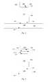
- Silicide layer 122which is preferably cobalt silicide or titanium silicide, is part of top conductor 400 , which further includes conductive layers such as, for example, titanium nitride layer 404 and tungsten layer 406 .
- conductive layerssuch as, for example, titanium nitride layer 404 and tungsten layer 406 .
- silicideis only formed where a silicide-forming metal is in contact with the silicon of diode 302 ; the cross-hatched portion of layer 122 is unreacted metal, not silicide.
- Top conductor 400which is shown slightly misaligned with underlying pillar 300 , is preferably rail-shaped, shown in cross-section extending out of the page.
- a monolithic three dimensional memory array formed above a substratecomprises at least a first memory level formed at a first height above the substrate and a second memory level formed at a second height different from the first height. Three, four, eight, or indeed any number of memory levels can be formed above the substrate in such a multilevel array.
Landscapes
- Physics & Mathematics (AREA)
- Condensed Matter Physics & Semiconductors (AREA)
- General Physics & Mathematics (AREA)
- Engineering & Computer Science (AREA)
- Computer Hardware Design (AREA)
- Microelectronics & Electronic Packaging (AREA)
- Power Engineering (AREA)
- Semiconductor Memories (AREA)
Abstract
Description
Claims (18)
Priority Applications (2)
| Application Number | Priority Date | Filing Date | Title |
|---|---|---|---|
| US13/229,747US8330250B2 (en) | 2003-12-03 | 2011-09-11 | P-I-N diode crystallized adjacent to a silicide in series with a dielectric material |
| US13/705,227US8633567B2 (en) | 2003-12-03 | 2012-12-05 | Devices including a P-I-N diode disposed adjacent a silicide in series with a dielectric material |
Applications Claiming Priority (4)
| Application Number | Priority Date | Filing Date | Title |
|---|---|---|---|
| US10/728,230US6946719B2 (en) | 2003-12-03 | 2003-12-03 | Semiconductor device including junction diode contacting contact-antifuse unit comprising silicide |
| US10/954,510US7176064B2 (en) | 2003-12-03 | 2004-09-29 | Memory cell comprising a semiconductor junction diode crystallized adjacent to a silicide |
| US11/560,289US8018024B2 (en) | 2003-12-03 | 2006-11-15 | P-i-n diode crystallized adjacent to a silicide in series with a dielectric antifuse |
| US13/229,747US8330250B2 (en) | 2003-12-03 | 2011-09-11 | P-I-N diode crystallized adjacent to a silicide in series with a dielectric material |
Related Parent Applications (1)
| Application Number | Title | Priority Date | Filing Date |
|---|---|---|---|
| US11/560,289ContinuationUS8018024B2 (en) | 2003-12-03 | 2006-11-15 | P-i-n diode crystallized adjacent to a silicide in series with a dielectric antifuse |
Related Child Applications (1)
| Application Number | Title | Priority Date | Filing Date |
|---|---|---|---|
| US13/705,227ContinuationUS8633567B2 (en) | 2003-12-03 | 2012-12-05 | Devices including a P-I-N diode disposed adjacent a silicide in series with a dielectric material |
Publications (2)
| Publication Number | Publication Date |
|---|---|
| US20120001296A1 US20120001296A1 (en) | 2012-01-05 |
| US8330250B2true US8330250B2 (en) | 2012-12-11 |
Family
ID=46326610
Family Applications (3)
| Application Number | Title | Priority Date | Filing Date |
|---|---|---|---|
| US11/560,289Expired - Fee RelatedUS8018024B2 (en) | 2003-12-03 | 2006-11-15 | P-i-n diode crystallized adjacent to a silicide in series with a dielectric antifuse |
| US13/229,747Expired - Fee RelatedUS8330250B2 (en) | 2003-12-03 | 2011-09-11 | P-I-N diode crystallized adjacent to a silicide in series with a dielectric material |
| US13/705,227Expired - LifetimeUS8633567B2 (en) | 2003-12-03 | 2012-12-05 | Devices including a P-I-N diode disposed adjacent a silicide in series with a dielectric material |
Family Applications Before (1)
| Application Number | Title | Priority Date | Filing Date |
|---|---|---|---|
| US11/560,289Expired - Fee RelatedUS8018024B2 (en) | 2003-12-03 | 2006-11-15 | P-i-n diode crystallized adjacent to a silicide in series with a dielectric antifuse |
Family Applications After (1)
| Application Number | Title | Priority Date | Filing Date |
|---|---|---|---|
| US13/705,227Expired - LifetimeUS8633567B2 (en) | 2003-12-03 | 2012-12-05 | Devices including a P-I-N diode disposed adjacent a silicide in series with a dielectric material |
Country Status (1)
| Country | Link |
|---|---|
| US (3) | US8018024B2 (en) |
Families Citing this family (24)
| Publication number | Priority date | Publication date | Assignee | Title |
|---|---|---|---|---|
| US7176064B2 (en)* | 2003-12-03 | 2007-02-13 | Sandisk 3D Llc | Memory cell comprising a semiconductor junction diode crystallized adjacent to a silicide |
| US7682920B2 (en)* | 2003-12-03 | 2010-03-23 | Sandisk 3D Llc | Method for making a p-i-n diode crystallized adjacent to a silicide in series with a dielectric antifuse |
| US8018024B2 (en) | 2003-12-03 | 2011-09-13 | Sandisk 3D Llc | P-i-n diode crystallized adjacent to a silicide in series with a dielectric antifuse |
| CN101553925B (en)* | 2006-11-15 | 2013-08-14 | 桑迪士克3D公司 | P-I-N Diode Crystallized Adjacent to Silicide in Series with Dielectric Antifuse and Method of Formation |
| FR2911431B1 (en)* | 2007-01-16 | 2009-05-15 | Soitec Silicon On Insulator | METHOD OF MANUFACTURING STRUCTURES WITH INSULATING LAYER OF CONTROLLED THICKNESS |
| US7684226B2 (en)* | 2007-06-25 | 2010-03-23 | Sandisk 3D Llc | Method of making high forward current diodes for reverse write 3D cell |
| EP2165336A1 (en)* | 2007-06-25 | 2010-03-24 | Sandisk 3D LLC | High forward current diodes for reverse write 3d cell and method of making thereof |
| US7830697B2 (en)* | 2007-06-25 | 2010-11-09 | Sandisk 3D Llc | High forward current diodes for reverse write 3D cell |
| US7800939B2 (en)* | 2007-06-29 | 2010-09-21 | Sandisk 3D Llc | Method of making 3D R/W cell with reduced reverse leakage |
| KR20100049564A (en)* | 2007-06-29 | 2010-05-12 | 쌘디스크 3디 엘엘씨 | 3d r/w cell with reduced reverse leakage and method of making thereof |
| US7759666B2 (en)* | 2007-06-29 | 2010-07-20 | Sandisk 3D Llc | 3D R/W cell with reduced reverse leakage |
| US7876597B2 (en) | 2007-09-19 | 2011-01-25 | Micron Technology, Inc. | NAND-structured series variable-resistance material memories, processes of forming same, and methods of using same |
| US9129845B2 (en)* | 2007-09-19 | 2015-09-08 | Micron Technology, Inc. | Buried low-resistance metal word lines for cross-point variable-resistance material memories |
| US8349663B2 (en)* | 2007-09-28 | 2013-01-08 | Sandisk 3D Llc | Vertical diode based memory cells having a lowered programming voltage and methods of forming the same |
| WO2009126846A1 (en)* | 2008-04-11 | 2009-10-15 | Sandisk 3D, Llc | Damascene integration methods for graphitic films in three-dimensional memories and memories formed therefrom |
| TW201001629A (en)* | 2008-04-11 | 2010-01-01 | Sandisk 3D Llc | Memory cell that includes a carbon nano-tube reversible resistance-switching element and methods of forming the same |
| WO2010009364A1 (en)* | 2008-07-18 | 2010-01-21 | Sandisk 3D, Llc | Carbon-based resistivity-switching materials and methods of forming the same |
| US8023310B2 (en)* | 2009-01-14 | 2011-09-20 | Sandisk 3D Llc | Nonvolatile memory cell including carbon storage element formed on a silicide layer |
| US8207064B2 (en) | 2009-09-17 | 2012-06-26 | Sandisk 3D Llc | 3D polysilicon diode with low contact resistance and method for forming same |
| US8045364B2 (en)* | 2009-12-18 | 2011-10-25 | Unity Semiconductor Corporation | Non-volatile memory device ion barrier |
| JP2011165854A (en) | 2010-02-09 | 2011-08-25 | Toshiba Corp | Memory device and method of manufacturing the same |
| US8699259B2 (en) | 2011-03-02 | 2014-04-15 | Sandisk 3D Llc | Non-volatile storage system using opposite polarity programming signals for MIM memory cell |
| US9425185B2 (en) | 2014-05-29 | 2016-08-23 | Globalfoundries Inc. | Self-healing electrostatic discharge power clamp |
| US9318622B1 (en) | 2015-06-23 | 2016-04-19 | International Business Machines Corporation | Fin-type PIN diode array |
Citations (46)
| Publication number | Priority date | Publication date | Assignee | Title |
|---|---|---|---|---|
| US5521423A (en) | 1993-04-19 | 1996-05-28 | Kawasaki Steel Corporation | Dielectric structure for anti-fuse programming element |
| US5693556A (en) | 1995-12-29 | 1997-12-02 | Cypress Semiconductor Corp. | Method of making an antifuse metal post structure |
| US5915167A (en) | 1997-04-04 | 1999-06-22 | Elm Technology Corporation | Three dimensional structure memory |
| US5962911A (en) | 1996-04-29 | 1999-10-05 | Vlsi Technology, Inc. | Semiconductor devices having amorphous silicon antifuse structures |
| US6034882A (en) | 1998-11-16 | 2000-03-07 | Matrix Semiconductor, Inc. | Vertically stacked field programmable nonvolatile memory and method of fabrication |
| US6100120A (en) | 1999-05-11 | 2000-08-08 | Advanced Micro Devices, Inc. | Method of locally forming a high-k dielectric gate insulator |
| US6420215B1 (en) | 2000-04-28 | 2002-07-16 | Matrix Semiconductor, Inc. | Three-dimensional memory array and method of fabrication |
| US6486065B2 (en) | 2000-12-22 | 2002-11-26 | Matrix Semiconductor, Inc. | Method of forming nonvolatile memory device utilizing a hard mask |
| US20030003632A1 (en) | 2000-12-22 | 2003-01-02 | Cleeves James M. | Formation of antifuse structure in a three dimensional memory |
| US6515888B2 (en) | 2000-08-14 | 2003-02-04 | Matrix Semiconductor, Inc. | Low cost three-dimensional memory array |
| US6525953B1 (en) | 2001-08-13 | 2003-02-25 | Matrix Semiconductor, Inc. | Vertically-stacked, field-programmable, nonvolatile memory and method of fabrication |
| US6534403B2 (en) | 2000-12-22 | 2003-03-18 | Matrix Semiconductor | Method of making a contact and via structure |
| US20030062594A1 (en) | 2001-10-01 | 2003-04-03 | Chin-Yang Chen | Anti-fuse structure with low on-state resistance and low off-state leakage |
| US6661691B2 (en) | 2002-04-02 | 2003-12-09 | Hewlett-Packard Development Company, L.P. | Interconnection structure and methods |
| US20040016991A1 (en) | 2000-04-28 | 2004-01-29 | Matrix Semiconductor, Inc. | Silicon nitride antifuse for use in diode-antifuse memory arrays |
| US6686646B2 (en) | 2002-02-15 | 2004-02-03 | Matrix Semiconductor, Inc. | Diverse band gap energy level semiconductor device |
| US6777773B2 (en) | 2000-08-14 | 2004-08-17 | Matrix Semiconductor, Inc. | Memory cell with antifuse layer formed at diode junction |
| US20040232509A1 (en) | 2003-05-19 | 2004-11-25 | Matrix Semiconductor, Inc. | Rail schottky device and method of making |
| US6853049B2 (en) | 2002-03-13 | 2005-02-08 | Matrix Semiconductor, Inc. | Silicide-silicon oxide-semiconductor antifuse device and method of making |
| US20050052915A1 (en)* | 2002-12-19 | 2005-03-10 | Matrix Semiconductor, Inc. | Nonvolatile memory cell without a dielectric antifuse having high- and low-impedance states |
| US20050121742A1 (en) | 2003-12-03 | 2005-06-09 | Matrix Semiconductor, Inc | Semiconductor device including junction diode contacting contact-antifuse unit comprising silicide |
| US20050158950A1 (en)* | 2002-12-19 | 2005-07-21 | Matrix Semiconductor, Inc. | Non-volatile memory cell comprising a dielectric layer and a phase change material in series |
| US6952043B2 (en) | 2002-06-27 | 2005-10-04 | Matrix Semiconductor, Inc. | Electrically isolated pillars in active devices |
| US6952030B2 (en) | 2002-12-19 | 2005-10-04 | Matrix Semiconductor, Inc. | High-density three-dimensional memory cell |
| US20050221200A1 (en) | 2004-04-01 | 2005-10-06 | Matrix Semiconductor, Inc. | Photomask features with chromeless nonprinting phase shifting window |
| US20050226067A1 (en)* | 2002-12-19 | 2005-10-13 | Matrix Semiconductor, Inc. | Nonvolatile memory cell operating by increasing order in polycrystalline semiconductor material |
| US6956278B2 (en) | 2003-06-30 | 2005-10-18 | Matrix Semiconductor, Inc. | Low-density, high-resistivity titanium nitride layer for use as a contact for low-leakage dielectric layers |
| US20060067117A1 (en) | 2004-09-29 | 2006-03-30 | Matrix Semiconductor, Inc. | Fuse memory cell comprising a diode, the diode serving as the fuse element |
| US20060249753A1 (en) | 2005-05-09 | 2006-11-09 | Matrix Semiconductor, Inc. | High-density nonvolatile memory array fabricated at low temperature comprising semiconductor diodes |
| US20060250836A1 (en)* | 2005-05-09 | 2006-11-09 | Matrix Semiconductor, Inc. | Rewriteable memory cell comprising a diode and a resistance-switching material |
| US20060250837A1 (en)* | 2005-05-09 | 2006-11-09 | Sandisk 3D, Llc | Nonvolatile memory cell comprising a diode and a resistance-switching material |
| US20070002603A1 (en) | 2005-07-01 | 2007-01-04 | Matrix Semiconductor, Inc. | Memory cell with high-K antifuse for reverse bias programming |
| US7172840B2 (en) | 2003-12-05 | 2007-02-06 | Sandisk Corporation | Photomask features with interior nonprinting window using alternating phase shifting |
| US7176064B2 (en) | 2003-12-03 | 2007-02-13 | Sandisk 3D Llc | Memory cell comprising a semiconductor junction diode crystallized adjacent to a silicide |
| US7180123B2 (en) | 2003-07-21 | 2007-02-20 | Macronix International Co., Ltd. | Method for programming programmable eraseless memory |
| US20070072360A1 (en) | 2005-09-28 | 2007-03-29 | Tanmay Kumar | Method for using a memory cell comprising switchable semiconductor memory element with trimmable resistance |
| US20070069217A1 (en) | 2003-12-03 | 2007-03-29 | Herner S B | P-i-n diode crystallized adjacent to a silicide in series with a dielectric anitfuse |
| US7224013B2 (en) | 2004-09-29 | 2007-05-29 | Sandisk 3D Llc | Junction diode comprising varying semiconductor compositions |
| US7265000B2 (en) | 1998-11-16 | 2007-09-04 | Sandisk 3D Llc | Vertically stacked field programmable nonvolatile memory and method of fabrication |
| US7307013B2 (en) | 2004-06-30 | 2007-12-11 | Sandisk 3D Llc | Nonselective unpatterned etchback to expose buried patterned features |
| US7314815B2 (en) | 2004-10-21 | 2008-01-01 | Macronix International Co., Ltd. | Manufacturing method of one-time programmable read only memory |
| US20080025118A1 (en) | 2006-07-31 | 2008-01-31 | Scheuerlein Roy E | Method for using a mixed-use memory array |
| US7405465B2 (en) | 2004-09-29 | 2008-07-29 | Sandisk 3D Llc | Deposited semiconductor structure to minimize n-type dopant diffusion and method of making |
| US7423304B2 (en) | 2003-12-05 | 2008-09-09 | Sandisck 3D Llc | Optimization of critical dimensions and pitch of patterned features in and above a substrate |
| US7575984B2 (en) | 2006-05-31 | 2009-08-18 | Sandisk 3D Llc | Conductive hard mask to protect patterned features during trench etch |
| US7682920B2 (en) | 2003-12-03 | 2010-03-23 | Sandisk 3D Llc | Method for making a p-i-n diode crystallized adjacent to a silicide in series with a dielectric antifuse |
Family Cites Families (4)
| Publication number | Priority date | Publication date | Assignee | Title |
|---|---|---|---|---|
| JPH08139197A (en) | 1994-11-11 | 1996-05-31 | Tadahiro Omi | Semiconductor device utilizing silicide reaction |
| US6534841B1 (en) | 2001-12-14 | 2003-03-18 | Hewlett-Packard Company | Continuous antifuse material in memory structure |
| JP4360826B2 (en) | 2003-04-24 | 2009-11-11 | シャープ株式会社 | Semiconductor film and manufacturing method thereof |
| JP2005347468A (en) | 2004-06-02 | 2005-12-15 | Matsushita Electric Ind Co Ltd | Nonvolatile memory |
- 2006
- 2006-11-15USUS11/560,289patent/US8018024B2/ennot_activeExpired - Fee Related
- 2011
- 2011-09-11USUS13/229,747patent/US8330250B2/ennot_activeExpired - Fee Related
- 2012
- 2012-12-05USUS13/705,227patent/US8633567B2/ennot_activeExpired - Lifetime
Patent Citations (51)
| Publication number | Priority date | Publication date | Assignee | Title |
|---|---|---|---|---|
| US5521423A (en) | 1993-04-19 | 1996-05-28 | Kawasaki Steel Corporation | Dielectric structure for anti-fuse programming element |
| US5693556A (en) | 1995-12-29 | 1997-12-02 | Cypress Semiconductor Corp. | Method of making an antifuse metal post structure |
| US5962911A (en) | 1996-04-29 | 1999-10-05 | Vlsi Technology, Inc. | Semiconductor devices having amorphous silicon antifuse structures |
| US5915167A (en) | 1997-04-04 | 1999-06-22 | Elm Technology Corporation | Three dimensional structure memory |
| US7319053B2 (en) | 1998-11-16 | 2008-01-15 | Sandisk 3D Llc | Vertically stacked field programmable nonvolatile memory and method of fabrication |
| US6034882A (en) | 1998-11-16 | 2000-03-07 | Matrix Semiconductor, Inc. | Vertically stacked field programmable nonvolatile memory and method of fabrication |
| US7265000B2 (en) | 1998-11-16 | 2007-09-04 | Sandisk 3D Llc | Vertically stacked field programmable nonvolatile memory and method of fabrication |
| US6100120A (en) | 1999-05-11 | 2000-08-08 | Advanced Micro Devices, Inc. | Method of locally forming a high-k dielectric gate insulator |
| US20040016991A1 (en) | 2000-04-28 | 2004-01-29 | Matrix Semiconductor, Inc. | Silicon nitride antifuse for use in diode-antifuse memory arrays |
| US6420215B1 (en) | 2000-04-28 | 2002-07-16 | Matrix Semiconductor, Inc. | Three-dimensional memory array and method of fabrication |
| US6777773B2 (en) | 2000-08-14 | 2004-08-17 | Matrix Semiconductor, Inc. | Memory cell with antifuse layer formed at diode junction |
| US6515888B2 (en) | 2000-08-14 | 2003-02-04 | Matrix Semiconductor, Inc. | Low cost three-dimensional memory array |
| US20030003632A1 (en) | 2000-12-22 | 2003-01-02 | Cleeves James M. | Formation of antifuse structure in a three dimensional memory |
| US6541312B2 (en) | 2000-12-22 | 2003-04-01 | Matrix Semiconductor, Inc. | Formation of antifuse structure in a three dimensional memory |
| US6534403B2 (en) | 2000-12-22 | 2003-03-18 | Matrix Semiconductor | Method of making a contact and via structure |
| US6486065B2 (en) | 2000-12-22 | 2002-11-26 | Matrix Semiconductor, Inc. | Method of forming nonvolatile memory device utilizing a hard mask |
| US6525953B1 (en) | 2001-08-13 | 2003-02-25 | Matrix Semiconductor, Inc. | Vertically-stacked, field-programmable, nonvolatile memory and method of fabrication |
| US20030062594A1 (en) | 2001-10-01 | 2003-04-03 | Chin-Yang Chen | Anti-fuse structure with low on-state resistance and low off-state leakage |
| US6686646B2 (en) | 2002-02-15 | 2004-02-03 | Matrix Semiconductor, Inc. | Diverse band gap energy level semiconductor device |
| US6853049B2 (en) | 2002-03-13 | 2005-02-08 | Matrix Semiconductor, Inc. | Silicide-silicon oxide-semiconductor antifuse device and method of making |
| US6661691B2 (en) | 2002-04-02 | 2003-12-09 | Hewlett-Packard Development Company, L.P. | Interconnection structure and methods |
| US6952043B2 (en) | 2002-06-27 | 2005-10-04 | Matrix Semiconductor, Inc. | Electrically isolated pillars in active devices |
| US6952030B2 (en) | 2002-12-19 | 2005-10-04 | Matrix Semiconductor, Inc. | High-density three-dimensional memory cell |
| US20050158950A1 (en)* | 2002-12-19 | 2005-07-21 | Matrix Semiconductor, Inc. | Non-volatile memory cell comprising a dielectric layer and a phase change material in series |
| US20050052915A1 (en)* | 2002-12-19 | 2005-03-10 | Matrix Semiconductor, Inc. | Nonvolatile memory cell without a dielectric antifuse having high- and low-impedance states |
| US20050226067A1 (en)* | 2002-12-19 | 2005-10-13 | Matrix Semiconductor, Inc. | Nonvolatile memory cell operating by increasing order in polycrystalline semiconductor material |
| US20040232509A1 (en) | 2003-05-19 | 2004-11-25 | Matrix Semiconductor, Inc. | Rail schottky device and method of making |
| US6956278B2 (en) | 2003-06-30 | 2005-10-18 | Matrix Semiconductor, Inc. | Low-density, high-resistivity titanium nitride layer for use as a contact for low-leakage dielectric layers |
| US7180123B2 (en) | 2003-07-21 | 2007-02-20 | Macronix International Co., Ltd. | Method for programming programmable eraseless memory |
| US20070069217A1 (en) | 2003-12-03 | 2007-03-29 | Herner S B | P-i-n diode crystallized adjacent to a silicide in series with a dielectric anitfuse |
| US20070105284A1 (en) | 2003-12-03 | 2007-05-10 | Herner S B | Method for forming a memory cell comprising a semiconductor junction diode crystallized adjacent to a silicide |
| US20100136751A1 (en) | 2003-12-03 | 2010-06-03 | Herner S Brad | Method for making a p-i-n diode crystallized adjacent to a silicide in series with a dielectric antifuse |
| US7682920B2 (en) | 2003-12-03 | 2010-03-23 | Sandisk 3D Llc | Method for making a p-i-n diode crystallized adjacent to a silicide in series with a dielectric antifuse |
| US6946719B2 (en) | 2003-12-03 | 2005-09-20 | Matrix Semiconductor, Inc | Semiconductor device including junction diode contacting contact-antifuse unit comprising silicide |
| US20050121742A1 (en) | 2003-12-03 | 2005-06-09 | Matrix Semiconductor, Inc | Semiconductor device including junction diode contacting contact-antifuse unit comprising silicide |
| US7176064B2 (en) | 2003-12-03 | 2007-02-13 | Sandisk 3D Llc | Memory cell comprising a semiconductor junction diode crystallized adjacent to a silicide |
| US7423304B2 (en) | 2003-12-05 | 2008-09-09 | Sandisck 3D Llc | Optimization of critical dimensions and pitch of patterned features in and above a substrate |
| US7172840B2 (en) | 2003-12-05 | 2007-02-06 | Sandisk Corporation | Photomask features with interior nonprinting window using alternating phase shifting |
| US20050221200A1 (en) | 2004-04-01 | 2005-10-06 | Matrix Semiconductor, Inc. | Photomask features with chromeless nonprinting phase shifting window |
| US7307013B2 (en) | 2004-06-30 | 2007-12-11 | Sandisk 3D Llc | Nonselective unpatterned etchback to expose buried patterned features |
| US7405465B2 (en) | 2004-09-29 | 2008-07-29 | Sandisk 3D Llc | Deposited semiconductor structure to minimize n-type dopant diffusion and method of making |
| US20060067117A1 (en) | 2004-09-29 | 2006-03-30 | Matrix Semiconductor, Inc. | Fuse memory cell comprising a diode, the diode serving as the fuse element |
| US7224013B2 (en) | 2004-09-29 | 2007-05-29 | Sandisk 3D Llc | Junction diode comprising varying semiconductor compositions |
| US7314815B2 (en) | 2004-10-21 | 2008-01-01 | Macronix International Co., Ltd. | Manufacturing method of one-time programmable read only memory |
| US20060249753A1 (en) | 2005-05-09 | 2006-11-09 | Matrix Semiconductor, Inc. | High-density nonvolatile memory array fabricated at low temperature comprising semiconductor diodes |
| US20060250837A1 (en)* | 2005-05-09 | 2006-11-09 | Sandisk 3D, Llc | Nonvolatile memory cell comprising a diode and a resistance-switching material |
| US20060250836A1 (en)* | 2005-05-09 | 2006-11-09 | Matrix Semiconductor, Inc. | Rewriteable memory cell comprising a diode and a resistance-switching material |
| US20070002603A1 (en) | 2005-07-01 | 2007-01-04 | Matrix Semiconductor, Inc. | Memory cell with high-K antifuse for reverse bias programming |
| US20070072360A1 (en) | 2005-09-28 | 2007-03-29 | Tanmay Kumar | Method for using a memory cell comprising switchable semiconductor memory element with trimmable resistance |
| US7575984B2 (en) | 2006-05-31 | 2009-08-18 | Sandisk 3D Llc | Conductive hard mask to protect patterned features during trench etch |
| US20080025118A1 (en) | 2006-07-31 | 2008-01-31 | Scheuerlein Roy E | Method for using a mixed-use memory array |
Non-Patent Citations (66)
| Title |
|---|
| Aug. 1, 2011 Reply to Jun. 8, 2011 Office Action of counterpart Chinese Patent Application Serial No. 200780042606.X. |
| Aug. 2, 2006 Reply to Office Action of related U.S. Appl. No. 10/954,510 mailed May 9, 2006. |
| Aug. 26, 2010 Reply to Jun. 28, 2010 Final Office Action of related U.S. Appl. No. 11/560,289. |
| Aug. 4, 2009 Preliminary Amendment of counterpart European Patent Application Serial No. 07 840 040.5. |
| Chiang, Steve et al., "Antifuse Structure Comparison for Field Programmable Gate Arrays", IEDM 92-611, (Apr. 1992), 24.6.1-24.6.4. |
| Dec. 10, 2009 Reply to Sep. 18, 2009 Office Action of related U.S. Appl. No. 11/613,151. |
| Dec. 17, 2009 Reply to Office Action of related U.S. Appl. No. 11/560,289 mailed Sep. 18, 2009. |
| Dec. 22, 2008 Reply to Aug. 21, 2008 Ex Parte Quayle Office Action of related U.S. Appl. No. 11/560,283. |
| Ex parte Quayle Office Action of related U.S. Appl. No. 11/613,151 mailed Mar. 6, 2008. |
| Feb. 1, 2011 Reply to Nov. 1, 2010 Office Action of related U.S. Appl. No. 12/698,253. |
| Final Office Action of related U.S. Appl. No. 11/560,289 mailed Jun. 28, 2010. |
| Final Office Action of related U.S. Appl. No. 11/613,151 mailed Feb. 23, 2010. |
| Hamdy, Esmat et al., "Dielectric Based Antifuse for Logic and Memory Ics", IEDM 88, (1988), 786-789. |
| Hatalis et al., "Large Grain Polycrystalline Silicon by Low-Temperature Annealing of Low-Pressure Chemical Vapor Deposited Amorphous Silicon Films,", J. Appl. Phys. 63(7), (Apr. 1, 1988), 2260-2266. |
| Herner et al., "Effect of Ohmic Contacts on Polysilicon Memory Effect," Proceedings of Materials Research Society, vol. 864, E5.6.1 (2005). |
| Herner et al., U.S. Appl. No. 10/326,470, filed Dec. 19, 2002. |
| Herner, S. B. et al. "Polycrystalline Silicon/CoSi2 Schottky Diode with Integrated SiO2 Antifuse: A Nonvolatile Memory Cell", Applied Physics Letter, vol. 82, No. 23, Jun. 9, 2003, 4163-4165. |
| Holloway et al., "Amorphous Ti-Si Alloy Formed by Interdiffusion of Amorphous Si and Crystalline Ti Multilayers," J. Appl. Phys. 61(4), (Feb. 15, 1987), 1359-1364. |
| International Preliminary Report on Patentability of counterpart PCT International Patent Application Serial No. PCT/US2007/023855 dated May 28, 2009. |
| International Search Report and Written Opinion of of counterpart PCT International Patent Application Serial No. PCT/US2007/023855 mailed May 7, 2008. |
| Jan. 30, 2009 Preliminary Amendment of related U.S. Appl. No. 11/560,289. |
| Jul. 10, 2009 Reply to Restriction Requirement of related U.S. Appl. No. 11/560,289 mailed Jun. 10, 2009. |
| Jul. 21, 2010 Reply to Office Action of counterpart Chinese Patent Application Serial No. 200780042606.X mailed Jun. 11, 2010. |
| Jul. 8, 2008 Reply to Restriction Requirement of related U.S. Appl. No. 11/560,283 mailed Jun. 4, 2008. |
| Jun. 24, 2009 Reply to Mar. 24, 2009 Office Action of related U.S. Appl. No. 11/560,283. |
| Kim et al., "Oxidation Behavior of a Patterned TiSi2/Polysilicon Stack," J. Vac. Sci. Technol. B 19(2), (Mar./Apr. 2001), 366-371. |
| Konakova, R.V. et al., "Ohmic Contacts for Microwave Diodes", Proc. 22nd International Conference on Microelectronics (MIEL 2000), vol. 2, NIS, Serbia, May 14-17, 2000, (Jan. 1999), 477-480. |
| Mar. 2, 2010 Office Action of counterpart European Patent Application Serial No. 07 840 040.5. |
| Mar. 29, 2006 Reply to Restriction Requirement of related U.S. Appl. No. 10/954,510 mailed Mar. 13, 2006. |
| May 24, 2010 Reply to Final Office Action of related U.S. Appl. No. 11/613,151 mailed Feb. 23, 2010. |
| May 24, 2010 Reply to Office Action of related U.S. Appl. No. 11/560,289 mailed Feb. 22, 2010. |
| May 6, 2009 Reply to Feb. 13, 2009 Office Action of related U.S. Appl. No. 11/613,151. |
| McPherson et al., "Proposed Universal Relationship Between Dielectric Breakdown and Dielectric Constant," Proceedings of 2003 IEDM, pp. 633-636. |
| Notice of Allowance in related U.S. Appl. No. 11/560,289 mailed May 17, 2011. |
| Notice of Allowance of related U.S. Appl. No. 10/728,230 dated May 13, 2005. |
| Notice of Allowance of related U.S. Appl. No. 10/954,510 mailed Oct. 19, 2006. |
| Notice of Allowance of related U.S. Appl. No. 11/560,283 mailed Nov. 2, 2009. |
| Notice of Allowance of related U.S. Appl. No. 11/560,283 mailed Sep. 3, 2009. |
| Notice of Allowance of related U.S. Appl. No. 11/613,151 mailed Jul. 1, 2009. |
| Notice of Allowance of related U.S. Appl. No. 11/613,151 mailed Jul. 16, 2010. |
| Notice of Allowance of related U.S. Appl. No. 11/613,151 mailed Sep. 24, 2008. |
| Notice of Allowance of related U.S. Appl. No. 12/698,253 dated Apr. 15, 2011. |
| Notice of Allowance of related U.S. Appl. No. 12/698,253 dated Feb. 16, 2011. |
| Office Action Ex Parte Quayle of related U.S. Appl. No. 11/560,283 mailed Aug. 21, 2008. |
| Office Action of counterpart Chinese Patent Application Serial No. 200780042606.X dated Sep. 4, 2012. |
| Office Action of counterpart Chinese Patent Application Serial No. 200780042606.X Issued Jan. 29, 2012. |
| Office Action of counterpart Chinese Patent Application Serial No. 200780042606.X mailed Jun. 11, 2010. |
| Office Action of counterpart Chinese Patent Application Serial No. 200780042606.X mailed Jun. 8, 2011. |
| Office Action of related U.S. Appl. No. 10/954,510 mailed May 9, 2006. |
| Office Action of related U.S. Appl. No. 11/560,283 mailed Mar. 24, 2009. |
| Office Action of related U.S. Appl. No. 11/560,289 mailed Feb. 22, 2010. |
| Office Action of related U.S. Appl. No. 11/560,289 mailed Sep. 18, 2009. |
| Office Action of related U.S. Appl. No. 11/613,151 mailed Feb. 13, 2009. |
| Office Action of related U.S. Appl. No. 11/613,151 mailed Sep. 18, 2009. |
| Office Action of related U.S. Appl. No. 12/698,253 mailed Nov. 1, 2010. |
| Response to Jan. 29, 2012 Office Action of counterpart Chinese Patent Application Serial No. 200780042606.X filed Apr. 9, 2012. |
| Restriction Requirement of related U.S. Appl. No. 10/954,510 mailed Mar. 13, 2006. |
| Restriction Requirement of related U.S. Appl. No. 11/560,283 mailed Jun. 4, 2008. |
| Restriction Requirement of related U.S. Appl. No. 11/560,289 mailed Jun. 10, 2009. |
| Restriction Requirement of related U.S. Appl. No. 12/698,253 mailed Aug. 27, 2010. |
| Sep. 14, 2010 Reply to Aug. 27, 2010 Restriction Requirement of related U.S. Appl. No. 12/698,253. |
| Sep. 8, 2008 Reply to Mar. 6, 2008 Ex Parte Quayle Office Action of related U.S. Appl. No. 11/613,151. |
| Shih, Chih-Ching et al., "Characterization and Modeling of a Highly Reliable Metal-to-Metal Antifuse for High-Performance and High-Density Field-Programmable Gate Arrays", 1977 IEEE, (Sep. 1997), 25-33. |
| Tang et al., "Twinning in TiSi2-Island Catalyzed Si Nanowires Grown by Gas-Source Molecular-Beam Epitaxy," Applied Physics Letters, vol. 81, No. 13, (Sep. 23, 2002), 2451-2453. |
| Tung, "Oxide Mediated Epitaxy of CoSi2 on Silicon," Appl. Phys. Lett. 68 (24), (Jun. 10, 1996), 3461-3463. |
| Wang, Shoue-Jen et al., "High-Performance Metal/Silicide Antifuse", IEEE Electron Device Letter, vol. 13, No. 9, Sep. 1992, 471-472. |
Also Published As
| Publication number | Publication date |
|---|---|
| US20130119510A1 (en) | 2013-05-16 |
| US20070069217A1 (en) | 2007-03-29 |
| US8633567B2 (en) | 2014-01-21 |
| US20120001296A1 (en) | 2012-01-05 |
| US8018024B2 (en) | 2011-09-13 |
Similar Documents
| Publication | Publication Date | Title |
|---|---|---|
| US7682920B2 (en) | Method for making a p-i-n diode crystallized adjacent to a silicide in series with a dielectric antifuse | |
| US8330250B2 (en) | P-I-N diode crystallized adjacent to a silicide in series with a dielectric material | |
| US8349663B2 (en) | Vertical diode based memory cells having a lowered programming voltage and methods of forming the same | |
| US7767499B2 (en) | Method to form upward pointing p-i-n diodes having large and uniform current | |
| US8737110B2 (en) | Large array of upward pointing P-I-N diodes having large and uniform current | |
| US7176064B2 (en) | Memory cell comprising a semiconductor junction diode crystallized adjacent to a silicide | |
| US8030740B2 (en) | Deposited semiconductor structure to minimize N-type dopant diffusion and method of making | |
| US20060249753A1 (en) | High-density nonvolatile memory array fabricated at low temperature comprising semiconductor diodes | |
| WO2008060543A2 (en) | P-i-n diode crystallized adjacent to a silicide in series with a dielectric antifuse and methods of forming the same | |
| JP2010510656A (en) | P-IN diode crystallized adjacent to silicide in series with dielectric antifuse and method of forming the same |
Legal Events
| Date | Code | Title | Description |
|---|---|---|---|
| STCF | Information on status: patent grant | Free format text:PATENTED CASE | |
| AS | Assignment | Owner name:SANDISK TECHNOLOGIES INC., TEXAS Free format text:ASSIGNMENT OF ASSIGNORS INTEREST;ASSIGNOR:SANDISK 3D LLC.;REEL/FRAME:038300/0665 Effective date:20160324 | |
| AS | Assignment | Owner name:SANDISK TECHNOLOGIES INC., TEXAS Free format text:CORRECTIVE ASSIGNMENT TO CORRECT THE INCORRECT LISTED PATENT NUMBER 8853569 TO THE CORRECT PATENT NUMBER 8883569 PREVIOUSLY RECORDED ON REEL 038300 FRAME 0665. ASSIGNOR(S) HEREBY CONFIRMS THE ASSIGNMENT;ASSIGNOR:SANDISK 3D LLC;REEL/FRAME:038520/0552 Effective date:20160324 | |
| AS | Assignment | Owner name:SANDISK TECHNOLOGIES LLC, TEXAS Free format text:CHANGE OF NAME;ASSIGNOR:SANDISK TECHNOLOGIES INC;REEL/FRAME:038807/0850 Effective date:20160516 | |
| FPAY | Fee payment | Year of fee payment:4 | |
| MAFP | Maintenance fee payment | Free format text:PAYMENT OF MAINTENANCE FEE, 8TH YEAR, LARGE ENTITY (ORIGINAL EVENT CODE: M1552); ENTITY STATUS OF PATENT OWNER: LARGE ENTITY Year of fee payment:8 | |
| FEPP | Fee payment procedure | Free format text:MAINTENANCE FEE REMINDER MAILED (ORIGINAL EVENT CODE: REM.); ENTITY STATUS OF PATENT OWNER: LARGE ENTITY | |
| LAPS | Lapse for failure to pay maintenance fees | Free format text:PATENT EXPIRED FOR FAILURE TO PAY MAINTENANCE FEES (ORIGINAL EVENT CODE: EXP.); ENTITY STATUS OF PATENT OWNER: LARGE ENTITY | |
| STCH | Information on status: patent discontinuation | Free format text:PATENT EXPIRED DUE TO NONPAYMENT OF MAINTENANCE FEES UNDER 37 CFR 1.362 | |
| FP | Lapsed due to failure to pay maintenance fee | Effective date:20241211 |