US8329262B2 - Dielectric film formation using inert gas excitation - Google Patents
Dielectric film formation using inert gas excitationDownload PDFInfo
- Publication number
- US8329262B2 US8329262B2US12/874,886US87488610AUS8329262B2US 8329262 B2US8329262 B2US 8329262B2US 87488610 AUS87488610 AUS 87488610AUS 8329262 B2US8329262 B2US 8329262B2
- Authority
- US
- United States
- Prior art keywords
- plasma
- silicon
- nitrogen
- substrate
- region
- Prior art date
- Legal status (The legal status is an assumption and is not a legal conclusion. Google has not performed a legal analysis and makes no representation as to the accuracy of the status listed.)
- Expired - Fee Related, expires
Links
Images


Classifications
- H—ELECTRICITY
- H01—ELECTRIC ELEMENTS
- H01L—SEMICONDUCTOR DEVICES NOT COVERED BY CLASS H10
- H01L21/00—Processes or apparatus adapted for the manufacture or treatment of semiconductor or solid state devices or of parts thereof
- H01L21/02—Manufacture or treatment of semiconductor devices or of parts thereof
- H01L21/02104—Forming layers
- H01L21/02107—Forming insulating materials on a substrate
- H01L21/02109—Forming insulating materials on a substrate characterised by the type of layer, e.g. type of material, porous/non-porous, pre-cursors, mixtures or laminates
- H01L21/02205—Forming insulating materials on a substrate characterised by the type of layer, e.g. type of material, porous/non-porous, pre-cursors, mixtures or laminates the layer being characterised by the precursor material for deposition
- H01L21/02208—Forming insulating materials on a substrate characterised by the type of layer, e.g. type of material, porous/non-porous, pre-cursors, mixtures or laminates the layer being characterised by the precursor material for deposition the precursor containing a compound comprising Si
- H01L21/02219—Forming insulating materials on a substrate characterised by the type of layer, e.g. type of material, porous/non-porous, pre-cursors, mixtures or laminates the layer being characterised by the precursor material for deposition the precursor containing a compound comprising Si the compound comprising silicon and nitrogen
- H01L21/02222—Forming insulating materials on a substrate characterised by the type of layer, e.g. type of material, porous/non-porous, pre-cursors, mixtures or laminates the layer being characterised by the precursor material for deposition the precursor containing a compound comprising Si the compound comprising silicon and nitrogen the compound being a silazane
- C—CHEMISTRY; METALLURGY
- C23—COATING METALLIC MATERIAL; COATING MATERIAL WITH METALLIC MATERIAL; CHEMICAL SURFACE TREATMENT; DIFFUSION TREATMENT OF METALLIC MATERIAL; COATING BY VACUUM EVAPORATION, BY SPUTTERING, BY ION IMPLANTATION OR BY CHEMICAL VAPOUR DEPOSITION, IN GENERAL; INHIBITING CORROSION OF METALLIC MATERIAL OR INCRUSTATION IN GENERAL
- C23C—COATING METALLIC MATERIAL; COATING MATERIAL WITH METALLIC MATERIAL; SURFACE TREATMENT OF METALLIC MATERIAL BY DIFFUSION INTO THE SURFACE, BY CHEMICAL CONVERSION OR SUBSTITUTION; COATING BY VACUUM EVAPORATION, BY SPUTTERING, BY ION IMPLANTATION OR BY CHEMICAL VAPOUR DEPOSITION, IN GENERAL
- C23C16/00—Chemical coating by decomposition of gaseous compounds, without leaving reaction products of surface material in the coating, i.e. chemical vapour deposition [CVD] processes
- C23C16/04—Coating on selected surface areas, e.g. using masks
- C23C16/045—Coating cavities or hollow spaces, e.g. interior of tubes; Infiltration of porous substrates
- C—CHEMISTRY; METALLURGY
- C23—COATING METALLIC MATERIAL; COATING MATERIAL WITH METALLIC MATERIAL; CHEMICAL SURFACE TREATMENT; DIFFUSION TREATMENT OF METALLIC MATERIAL; COATING BY VACUUM EVAPORATION, BY SPUTTERING, BY ION IMPLANTATION OR BY CHEMICAL VAPOUR DEPOSITION, IN GENERAL; INHIBITING CORROSION OF METALLIC MATERIAL OR INCRUSTATION IN GENERAL
- C23C—COATING METALLIC MATERIAL; COATING MATERIAL WITH METALLIC MATERIAL; SURFACE TREATMENT OF METALLIC MATERIAL BY DIFFUSION INTO THE SURFACE, BY CHEMICAL CONVERSION OR SUBSTITUTION; COATING BY VACUUM EVAPORATION, BY SPUTTERING, BY ION IMPLANTATION OR BY CHEMICAL VAPOUR DEPOSITION, IN GENERAL
- C23C16/00—Chemical coating by decomposition of gaseous compounds, without leaving reaction products of surface material in the coating, i.e. chemical vapour deposition [CVD] processes
- C23C16/22—Chemical coating by decomposition of gaseous compounds, without leaving reaction products of surface material in the coating, i.e. chemical vapour deposition [CVD] processes characterised by the deposition of inorganic material, other than metallic material
- C23C16/30—Deposition of compounds, mixtures or solid solutions, e.g. borides, carbides, nitrides
- C23C16/34—Nitrides
- C23C16/345—Silicon nitride
- C—CHEMISTRY; METALLURGY
- C23—COATING METALLIC MATERIAL; COATING MATERIAL WITH METALLIC MATERIAL; CHEMICAL SURFACE TREATMENT; DIFFUSION TREATMENT OF METALLIC MATERIAL; COATING BY VACUUM EVAPORATION, BY SPUTTERING, BY ION IMPLANTATION OR BY CHEMICAL VAPOUR DEPOSITION, IN GENERAL; INHIBITING CORROSION OF METALLIC MATERIAL OR INCRUSTATION IN GENERAL
- C23C—COATING METALLIC MATERIAL; COATING MATERIAL WITH METALLIC MATERIAL; SURFACE TREATMENT OF METALLIC MATERIAL BY DIFFUSION INTO THE SURFACE, BY CHEMICAL CONVERSION OR SUBSTITUTION; COATING BY VACUUM EVAPORATION, BY SPUTTERING, BY ION IMPLANTATION OR BY CHEMICAL VAPOUR DEPOSITION, IN GENERAL
- C23C16/00—Chemical coating by decomposition of gaseous compounds, without leaving reaction products of surface material in the coating, i.e. chemical vapour deposition [CVD] processes
- C23C16/44—Chemical coating by decomposition of gaseous compounds, without leaving reaction products of surface material in the coating, i.e. chemical vapour deposition [CVD] processes characterised by the method of coating
- C23C16/448—Chemical coating by decomposition of gaseous compounds, without leaving reaction products of surface material in the coating, i.e. chemical vapour deposition [CVD] processes characterised by the method of coating characterised by the method used for generating reactive gas streams, e.g. by evaporation or sublimation of precursor materials
- C23C16/452—Chemical coating by decomposition of gaseous compounds, without leaving reaction products of surface material in the coating, i.e. chemical vapour deposition [CVD] processes characterised by the method of coating characterised by the method used for generating reactive gas streams, e.g. by evaporation or sublimation of precursor materials by activating reactive gas streams before their introduction into the reaction chamber, e.g. by ionisation or addition of reactive species
- C—CHEMISTRY; METALLURGY
- C23—COATING METALLIC MATERIAL; COATING MATERIAL WITH METALLIC MATERIAL; CHEMICAL SURFACE TREATMENT; DIFFUSION TREATMENT OF METALLIC MATERIAL; COATING BY VACUUM EVAPORATION, BY SPUTTERING, BY ION IMPLANTATION OR BY CHEMICAL VAPOUR DEPOSITION, IN GENERAL; INHIBITING CORROSION OF METALLIC MATERIAL OR INCRUSTATION IN GENERAL
- C23C—COATING METALLIC MATERIAL; COATING MATERIAL WITH METALLIC MATERIAL; SURFACE TREATMENT OF METALLIC MATERIAL BY DIFFUSION INTO THE SURFACE, BY CHEMICAL CONVERSION OR SUBSTITUTION; COATING BY VACUUM EVAPORATION, BY SPUTTERING, BY ION IMPLANTATION OR BY CHEMICAL VAPOUR DEPOSITION, IN GENERAL
- C23C16/00—Chemical coating by decomposition of gaseous compounds, without leaving reaction products of surface material in the coating, i.e. chemical vapour deposition [CVD] processes
- C23C16/56—After-treatment
- H—ELECTRICITY
- H01—ELECTRIC ELEMENTS
- H01J—ELECTRIC DISCHARGE TUBES OR DISCHARGE LAMPS
- H01J37/00—Discharge tubes with provision for introducing objects or material to be exposed to the discharge, e.g. for the purpose of examination or processing thereof
- H01J37/32—Gas-filled discharge tubes
- H01J37/32009—Arrangements for generation of plasma specially adapted for examination or treatment of objects, e.g. plasma sources
- H01J37/32357—Generation remote from the workpiece, e.g. down-stream
- H—ELECTRICITY
- H01—ELECTRIC ELEMENTS
- H01J—ELECTRIC DISCHARGE TUBES OR DISCHARGE LAMPS
- H01J37/00—Discharge tubes with provision for introducing objects or material to be exposed to the discharge, e.g. for the purpose of examination or processing thereof
- H01J37/32—Gas-filled discharge tubes
- H01J37/32431—Constructional details of the reactor
- H01J37/3244—Gas supply means
- H01J37/32449—Gas control, e.g. control of the gas flow
- H—ELECTRICITY
- H01—ELECTRIC ELEMENTS
- H01L—SEMICONDUCTOR DEVICES NOT COVERED BY CLASS H10
- H01L21/00—Processes or apparatus adapted for the manufacture or treatment of semiconductor or solid state devices or of parts thereof
- H01L21/02—Manufacture or treatment of semiconductor devices or of parts thereof
- H01L21/02104—Forming layers
- H01L21/02107—Forming insulating materials on a substrate
- H01L21/02109—Forming insulating materials on a substrate characterised by the type of layer, e.g. type of material, porous/non-porous, pre-cursors, mixtures or laminates
- H01L21/02112—Forming insulating materials on a substrate characterised by the type of layer, e.g. type of material, porous/non-porous, pre-cursors, mixtures or laminates characterised by the material of the layer
- H01L21/02123—Forming insulating materials on a substrate characterised by the type of layer, e.g. type of material, porous/non-porous, pre-cursors, mixtures or laminates characterised by the material of the layer the material containing silicon
- H01L21/02164—Forming insulating materials on a substrate characterised by the type of layer, e.g. type of material, porous/non-porous, pre-cursors, mixtures or laminates characterised by the material of the layer the material containing silicon the material being a silicon oxide, e.g. SiO2
- H—ELECTRICITY
- H01—ELECTRIC ELEMENTS
- H01L—SEMICONDUCTOR DEVICES NOT COVERED BY CLASS H10
- H01L21/00—Processes or apparatus adapted for the manufacture or treatment of semiconductor or solid state devices or of parts thereof
- H01L21/02—Manufacture or treatment of semiconductor devices or of parts thereof
- H01L21/02104—Forming layers
- H01L21/02107—Forming insulating materials on a substrate
- H01L21/02109—Forming insulating materials on a substrate characterised by the type of layer, e.g. type of material, porous/non-porous, pre-cursors, mixtures or laminates
- H01L21/02112—Forming insulating materials on a substrate characterised by the type of layer, e.g. type of material, porous/non-porous, pre-cursors, mixtures or laminates characterised by the material of the layer
- H01L21/02123—Forming insulating materials on a substrate characterised by the type of layer, e.g. type of material, porous/non-porous, pre-cursors, mixtures or laminates characterised by the material of the layer the material containing silicon
- H01L21/0217—Forming insulating materials on a substrate characterised by the type of layer, e.g. type of material, porous/non-porous, pre-cursors, mixtures or laminates characterised by the material of the layer the material containing silicon the material being a silicon nitride not containing oxygen, e.g. SixNy or SixByNz
- H—ELECTRICITY
- H01—ELECTRIC ELEMENTS
- H01L—SEMICONDUCTOR DEVICES NOT COVERED BY CLASS H10
- H01L21/00—Processes or apparatus adapted for the manufacture or treatment of semiconductor or solid state devices or of parts thereof
- H01L21/02—Manufacture or treatment of semiconductor devices or of parts thereof
- H01L21/02104—Forming layers
- H01L21/02107—Forming insulating materials on a substrate
- H01L21/02225—Forming insulating materials on a substrate characterised by the process for the formation of the insulating layer
- H01L21/0226—Forming insulating materials on a substrate characterised by the process for the formation of the insulating layer formation by a deposition process
- H01L21/02263—Forming insulating materials on a substrate characterised by the process for the formation of the insulating layer formation by a deposition process deposition from the gas or vapour phase
- H01L21/02271—Forming insulating materials on a substrate characterised by the process for the formation of the insulating layer formation by a deposition process deposition from the gas or vapour phase deposition by decomposition or reaction of gaseous or vapour phase compounds, i.e. chemical vapour deposition
- H01L21/02274—Forming insulating materials on a substrate characterised by the process for the formation of the insulating layer formation by a deposition process deposition from the gas or vapour phase deposition by decomposition or reaction of gaseous or vapour phase compounds, i.e. chemical vapour deposition in the presence of a plasma [PECVD]
- H—ELECTRICITY
- H01—ELECTRIC ELEMENTS
- H01L—SEMICONDUCTOR DEVICES NOT COVERED BY CLASS H10
- H01L21/00—Processes or apparatus adapted for the manufacture or treatment of semiconductor or solid state devices or of parts thereof
- H01L21/02—Manufacture or treatment of semiconductor devices or of parts thereof
- H01L21/02104—Forming layers
- H01L21/02107—Forming insulating materials on a substrate
- H01L21/02296—Forming insulating materials on a substrate characterised by the treatment performed before or after the formation of the layer
- H01L21/02318—Forming insulating materials on a substrate characterised by the treatment performed before or after the formation of the layer post-treatment
- H01L21/02321—Forming insulating materials on a substrate characterised by the treatment performed before or after the formation of the layer post-treatment introduction of substances into an already existing insulating layer
- H01L21/02323—Forming insulating materials on a substrate characterised by the treatment performed before or after the formation of the layer post-treatment introduction of substances into an already existing insulating layer introduction of oxygen
- H01L21/02326—Forming insulating materials on a substrate characterised by the treatment performed before or after the formation of the layer post-treatment introduction of substances into an already existing insulating layer introduction of oxygen into a nitride layer, e.g. changing SiN to SiON
- H—ELECTRICITY
- H01—ELECTRIC ELEMENTS
- H01J—ELECTRIC DISCHARGE TUBES OR DISCHARGE LAMPS
- H01J2237/00—Discharge tubes exposing object to beam, e.g. for analysis treatment, etching, imaging
- H01J2237/32—Processing objects by plasma generation
- H01J2237/33—Processing objects by plasma generation characterised by the type of processing
- H01J2237/332—Coating
- H01J2237/3322—Problems associated with coating
- H01J2237/3327—Coating high aspect ratio workpieces
Definitions
- Semiconductor device geometrieshave dramatically decreased in size since their introduction several decades ago. Modern semiconductor fabrication equipment routinely produces devices with 45 nm, 32 nm, and 28 nm feature sizes, and new equipment is being developed and implemented to make devices with even smaller geometries.
- the decreasing feature sizesresult in structural features on the device having decreased spatial dimensions.
- the widths of gaps and trenches on the devicenarrow to a point where the aspect ratio of gap depth to its width becomes high enough to make it challenging to fill the gap with dielectric material.
- the depositing dielectric materialis prone to clog at the top before the gap completely fills, producing a void or seam in the middle of the gap.
- the hardening processincludes a heat treatment to remove carbon and hydroxyl groups from the deposited material to leave behind a solid dielectric such as silicon oxide.
- a solid dielectricsuch as silicon oxide.
- the departing carbon and hydroxyl speciesoften leave behind pores in the hardened dielectric that reduce the quality of the final material.
- the hardening dielectricalso tends to shrink in volume, which can leave cracks and spaces at the interface of the dielectric and the surrounding substrate. In some instances, the volume of the hardened dielectric can decrease by 40% or more.
- the methodsinclude the steps of mixing a carbon-free silicon-containing precursor with plasma effluents, and depositing a silicon-and-nitrogen-containing layer on a substrate.
- the silicon-and-nitrogen-containing layersmay be made flowable or conformal by selection of the flow rate of excited effluents from a remote plasma region into the substrate processing region.
- the plasma effluentsare formed in a plasma by flowing inert gas(es) into the plasma.
- the silicon-and-nitrogen-containing layermay be converted to a silicon-and-oxygen-containing layer by curing and annealing the film.
- Embodiments of the inventioninclude methods of forming a silicon-and-nitrogen-containing layer on a substrate in a substrate processing region in a substrate processing chamber.
- the methodsinclude flowing a gas into a plasma region to produce excited effluents, wherein the combination of all gases in the plasma region during deposition consist essentially of inert gases which do not form chemical bonds within the silicon-and-nitrogen-containing layer.
- the methodsfurther include combining a carbon-free silicon-containing precursor with the plasma effluents in the substrate processing region such that the excited effluents cause a reaction in the carbon-free silicon-containing precursor to deposit the silicon-and-nitrogen-containing layer on the substrate.
- FIG. 1is a flowchart illustrating selected steps for making a silicon oxide film according to embodiments of the invention.
- FIG. 2is another flowchart illustrating selected steps for forming a silicon oxide film in a substrate gap according to embodiments of the invention.
- FIG. 3shows a substrate processing system according to embodiments of the invention.
- FIG. 4Ashows a substrate processing chamber according to embodiments of the invention.
- FIG. 4Bshows a showerhead of a substrate processing chamber according to embodiments of the invention.
- the methodsinclude the steps of mixing a carbon-free silicon-containing precursor with plasma effluents, and depositing a silicon-and-nitrogen-containing layer on a substrate.
- the silicon-and-nitrogen-containing layersmay be made flowable or conformal by selection of the flow rate of excited effluents from a remote plasma region into the substrate processing region.
- the plasma effluentsare formed in a plasma by flowing inert gas(es) into the plasma.
- the silicon-and-nitrogen-containing layermay be converted to a silicon-and-oxygen-containing layer by curing and annealing the film.
- Inert gasesare frequently used to initiate and increase the intensity of a plasma which contain additional material.
- the additional materialis excited in the plasma and reacts to deposit or react, forming a layer on a substrate.
- plasma-excited inert gasesi.e. excited plasma effluents
- excited plasma effluentshave been found to provide the excitation necessary to crack a carbon-free silicon-containing precursor and form a layer on a substrate. This occurs despite the fact that the carbon-free silicon-containing precursor is not directly excited by a plasma in the substrate processing region.
- modifying the flux of the excited plasma effluents entering the substrate processing regionchanges the flowability of the nascent film.
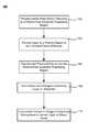
- FIG. 1is a flowchart showing selected steps in methods 100 of making silicon oxide films according to embodiments of the invention.
- the method 100includes providing a carbon-free silicon-containing precursor to a substrate processing region 102 .
- the carbon-free silicon-containing precursormay be, for example, a silicon-and-nitrogen precursor, a silicon-and-hydrogen precursor, or a silicon-nitrogen-and-hydrogen-containing precursor, among other classes of silicon-containing precursors.
- the silicon-precursormay be oxygen-free in addition to carbon-free. The lack of oxygen results in a lower concentration of silanol (Si—OH) groups in the silicon-and-nitrogen layer formed from the precursors. Excess silanol moieties in the deposited film can cause increased porosity and shrinkage during post deposition steps that remove the hydroxyl (—OH) moieties from the deposited layer.
- carbon-free silicon-containing precursorsmay include silyl-amines such as H 2 N(SiH 3 ), HN(SiH 3 ) 2 , and N(SiH 3 ) 3 , among other silyl-amines.
- the flow rates of a silyl-aminemay be greater than or about 200 sccm, greater than or about 300 sccm or greater than or about 500 sccm in different embodiments. All flow rates given herein refer to a dual chamber substrate processing system. Single wafer systems would require half these flow rates and other wafer sizes would require flow rates scaled by the processed area.
- These silyl-aminesmay be mixed with additional gases that may act as carrier gases, reactive gases, or both.
- Examplary additional gasesmay include H 2 , N 2 , NH 3 , He, and Ar, among other gases.
- Examples of carbon-free silicon-containing precursorsmay also include silane (SiH 4 ) either alone or mixed with other silicon (e.g., N(SiH 3 ) 3 ), hydrogen (e.g., H 2 ), and/or nitrogen (e.g., N 2 , NH 3 ) containing gases.
- Carbon-free silicon-containing precursorsmay also include disilane, trisilane, even higher-order silanes, and chlorinated silanes, alone or in combination with one another or the previously mentioned carbon-free silicon-containing precursors.
- the carbon-free silicon-containing precursoris not excited in a plasma region (e.g. a remote plasma region) before entering the plasma-free substrate processing region.
- Argonis delivered to a plasma region to form excited plasma effluents 104 .
- the excited plasma effluentsare generated in a plasma region separated from the substrate processing region such that the carbon-free silicon-containing precursor is essentially unexcited, directly, by the plasma.
- the argonmay be activated in a chamber plasma region or a remote plasma system (RPS) outside the processing chamber to form the excited plasma effluents, which are then transported into the substrate processing region 106 .
- the flow rate of the hydrogenmay be greater than or about 500 sccm, greater than or about 1 slm or greater than or about 1.5 slm in different embodiments.
- the plasma regionis filled with entirely or mostly argon. Other inert gases may be added and small to trace amounts of reactive species may also be present without compromising the methods or deviating from the intended scope of the invention.
- the excited plasma effluentsare generated in a section of the substrate processing region partitioned from a deposition region.
- the precursorsmix and react to deposit the silicon-and-nitrogen layer on a deposition substrate (e.g., a semiconductor wafer).
- the excited plasma effluentsare also accompanied by a unexcited inert gases (in the exemplary case, argon).
- the substrate processing regionmay be described herein as “plasma-free” during the growth of the silicon-and-nitrogen-containing layer, for example. “Plasma-free” does not necessarily mean the region is devoid of plasma.
- Ionized species and free electrons created within the plasma regiondo travel through pores (apertures) in the partition (showerhead) but the carbon-free silicon-containing precursor is not substantially excited by the plasma power applied to the plasma region.
- the borders of the plasma in the chamber plasma regionare hard to define and may encroach upon the substrate processing region through the apertures in the showerhead.
- a small amount of ionizationmay be effected within the substrate processing region directly.
- a low intensity plasmamay be created in the substrate processing region without eliminating desirable features of the forming film. All causes for a plasma having much lower ion density than the chamber plasma region (or a remote plasma region, for that matter) during the creation of the excited plasma effluents do not deviate from the scope of “plasma-free” as used herein.
- the carbon-free silicon-containing precursor and the excited plasma effluentsmix and react to form a silicon-and-nitrogen-containing film on the deposition substrate 108 .
- the deposited silicon-and-nitrogen-containing filmmay deposit conformally with recipe combinations which result in low deposition rates.
- the deposited silicon-and-nitrogen-containing filmhas flowable characteristics unlike conventional silicon nitride (Si 3 N 4 ) film deposition techniques. The flowable nature of the formation allows the film to flow into narrow gaps trenches and other structures on the deposition surface of the substrate.
- Conformal depositionmay result from a larger flow of excited plasma effluents caused by relatively large holes in the showerhead partition, increased plasma intensity and/or a shortened/widened path from a remote plasma region to the substrate processing region.
- flowable depositionmay result from a reduced flow of excited plasma effluents resulting from relatively small holes in the showerhead, decreased plasma intensity and/or a lengthened/narrowed/obstructed path from remote plasma region to substrate processing region.
- flowabilitymay result from a variety of properties which arise from mixing a excited plasma effluents with carbon-free silicon-containing precursor. These properties may include the presence of short chained polysilazane polymers. These short chains may grow and network to form more dense dielectric material during and after the formation of the film.
- the deposited filmmay have a silazane-type, Si—NH—Si backbone (i.e., a Si—N—H film).
- the deposited silicon-and-nitrogen-containing filmis also substantially carbon-free.
- carbon-freedoes not necessarily mean the film lacks even trace amounts of carbon.
- Carbon contaminantsmay be present in the precursor materials that find their way into the deposited silicon-and-nitrogen precursor. The amount of these carbon impurities however are much less than would be found in a silicon-containing precursor having a carbon moiety (e.g., TEOS, TMDSO, etc.).
- a silicon-containing precursor having a carbon moietye.g., TEOS, TMDSO, etc.
- the deposition substratemay be cured and/or annealed in oxygen-containing atmosphere(s) 110 .
- the curingmay occur in an ozone-containing atmosphere at a substrate temperature below or about 400° C. Under some conditions (e.g. between substrate temperatures from about 100° C. to about 200° C.) the conversion has been found to be substantially complete so a relatively high temperature anneal in an oxygen-containing environment may be unnecessary in embodiments.
- itmay be desirable to anneal the substrate in an oxygen-containing atmosphere to further convert the film to silicon oxide.
- the oxygen-containing atmospheremay include one or more oxygen-containing gases such as molecular oxygen (O 2 ), ozone (O 3 ), water vapor (H 2 O), hydrogen peroxide (H 2 O 2 ) and nitrogen-oxides (NO, NO 2 , etc.), among other oxygen-containing gases.
- the oxygen-containing atmospheremay also include radical oxygen and hydroxyl species such as atomic oxygen (O), hydroxides (OH), etc., that may be generated remotely and transported into the substrate chamber. Ions of oxygen-containing species may also be present.
- the oxygen anneal temperature of the substratemay be between about 500° C. and about 1100° C. The temperature of the substrate is above or about 600° C.
- Plasma excitationwhen employed, may be in the substrate processing region, in a separate region separated by a showerhead or in a remote plasma system (RPS).
- RPSremote plasma system
- the oxygen-containing atmospheres of both the curing and oxygen annealprovide oxygen to convert the silicon-and-nitrogen-containing film into the silicon oxide film.
- the lack of carbon in the silicon-and-nitrogen-containing filmresults in significantly fewer pores formed in the final silicon oxide film. It also results in less volume reduction (i.e., shrinkage) of the film during the conversion to the silicon oxide.
- shrinkagei.e., shrinkage
- inert gasesmay be used in place of argon and include neon, helium and xenon. Changing from argon to another inert gas changes the impedance of the gas within a plasma region and therefore may require alteration of the plasma region design and/or the plasma power supply. The matching circuit affiliated with the plasma power supply may adjust or be adjusted in response to the altered impedance. Combinations of inert gases may also be used. Inert gases are not restricted to noble gases disclosed hereto and more generally include all molecules which do not form chemical bonds within the silicon-and-nitrogen-containing film. Trace amounts of the inert gases may be incorporated in the film by one mechanism or another and still be considered inert by this definition.
- All gases in the plasma region during depositionconsist essentially of inert gases which do not form chemical bonds within the silicon-and-nitrogen-containing layer allowing for the presence of trace amounts of reactive gases without deviating from the intended claim scope herein.
- All gases in the plasma region during depositionconsist essentially of noble gases, in another disclosed embodiment.
- Excited plasma effluentsinclude ionized species, free electrons and electronically excited species whose electrons are still considered bound to the inert gas. As the excited plasma effluents travel from the plasma region to the substrate processing region, they may deexcite and reexcite through collisions with other effluents including unexcited plasma effluents. Therefore excited plasma effluents may not be excited during their entire journey towards the substrate yet may still participate in the excitation of the carbon-free silicon-and-nitrogen containing precursor.
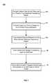
- the method 200includes transferring a substrate comprising a gap into a substrate processing region (operation 202 ).
- the substratehas gaps for the spacing and structure of device components (e.g., transistors) formed on the substrate.
- the gapsmay have a height and width that define an aspect ratio (AR) of the height to the width (i.e., H/W) that is significantly greater than 1:1 (e.g., 5:1 or more, 6:1 or more, 7:1 or more, 8:1 or more, 9:1 or more, 10:1 or more, 11:1 or more, 12:1 or more, etc.).
- ARaspect ratio
- the high ARis due to small gap widths of that range from about 90 nm to about 22 nm or less.
- the width of gapsmay be less than 100 nm, 50 nm, 35 nm, 30 nm, 25 nm or 20 nm, and the height of the gaps may be greater than 50 nm, 100 nm, 150 nm, 200 nm, 300 nm or 500 nm, in different embodiments.
- Argonis excited in a chamber plasma region to form excited plasma effluents 204 .
- the plasmacreates plasma effluents which flow through apertures in a showerhead separating the plasma region from the substrate processing region.
- a carbon-free silicon-containing precursoris mixed with the excited plasma effluents in the substrate processing region (operation 206 ).
- a flowable silicon-and-nitrogen-containing layeris deposited on the substrate (operation 208 ). Because the layer is flowable, it can fill the gaps having the high aspect ratios without creating voids or weak seams around the center of the filling material. For example, a depositing flowable material is less likely to prematurely clog the top of a gap before it is completely filled to leave a void in the middle of the gap.
- the silicon-and-nitrogen-containing layer in the trenchis substantially void-free, in embodiments.
- the as-deposited silicon-and-nitrogen-containing layermay then be cured in an ozone-containing atmosphere and/or annealed in an oxygen-containing atmosphere (operation 210 ) to transition the silicon-and-nitrogen-containing layer to silicon oxide.
- a further anneal(not shown) may be carried out in an inert environment at a higher substrate temperature in order to densify the silicon oxide layer. Curing and annealing the as-deposited silicon-and-nitrogen-containing layer in an oxygen-containing atmosphere forms a silicon oxide layer on the substrate, including within the substrate gap.
- the processing parameters of operation 210possess the same ranges described with reference to FIG. 1 .
- the silicon oxide layerhas fewer pores and less volume reduction than similar layers formed with carbon-containing precursors that have significant quantities of carbon present in the layer before the heat treatment step.
- the volume reductionis slight enough (e.g., about 17 vol. % or less) to avoid post heat treatment steps to fill, heal, or otherwise eliminate spaces that form in the gap as a result of the shrinking silicon oxide.
- Deposition chambersmay include high-density plasma chemical vapor deposition (HDP-CVD) chambers, plasma enhanced chemical vapor deposition (PECVD) chambers, sub-atmospheric chemical vapor deposition (SACVD) chambers, and thermal chemical vapor deposition chambers, among other types of chambers.
- HDP-CVDhigh-density plasma chemical vapor deposition
- PECVDplasma enhanced chemical vapor deposition
- SACVDsub-atmospheric chemical vapor deposition
- thermal chemical vapor deposition chambersamong other types of chambers.
- Specific examples of CVD systemsinclude the CENTURA ULTIMA® HDP-CVD chambers/systems, and PRODUCER® PECVD chambers/systems, available from Applied Materials, Inc. of Santa Clara, Calif.
- Examples of substrate processing chambers that can be used with exemplary methods of the inventionmay include those shown and described in co-assigned U.S. Provisional Patent App. No. 60/803,499 to Lubomirsky et al, filed May 30, 2006, and titled “PROCESS CHAMBER FOR DIELECTRIC GAPFILL,” the entire contents of which is herein incorporated by reference for all purposes. Additional exemplary systems may include those shown and described in U.S. Pat. Nos. 6,387,207 and 6,830,624, which are also incorporated herein by reference for all purposes.
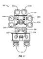
- FIG. 3shows one such system 300 of deposition, baking and curing chambers according to disclosed embodiments.
- a pair of FOUPs (front opening unified pods) 302supply substrate substrates (e.g., 300 mm diameter wafers) that are received by robotic arms 304 and placed into a low pressure holding area 406 before being placed into one of the wafer processing chambers 308 a - f .
- a second robotic arm 310may be used to transport the substrate wafers from the holding area 306 to the processing chambers 308 a - f and back.
- the processing chambers 308 a - fmay include one or more system components for depositing, annealing, curing and/or etching a flowable dielectric film on the substrate wafer.
- two pairs of the processing chambere.g., 308 c - d and 308 e - f
- the third pair of processing chamberse.g., 308 a - b
- the same two pairs of processing chambersmay be configured to both deposit and anneal a flowable dielectric film on the substrate, while the third pair of chambers (e.g., 308 a - b ) may be used for UV or E-beam curing of the deposited film.
- all three pairs of chamberse.g., 308 a - f ) may be configured to deposit and cure a flowable dielectric film on the substrate.
- two pairs of processing chambersmay be used for both deposition and UV or E-beam curing of the flowable dielectric, while a third pair of processing chambers (e.g. 308 a - b ) may be used for annealing the dielectric film.
- Any one or more of the processes describedmay be carried out on chamber(s) separated from the fabrication system shown in different embodiments.
- one or more of the process chambers 308 a - fmay be configured as a wet treatment chamber. These process chambers include heating the flowable dielectric film in an atmosphere that include moisture.
- embodiments of system 300may include wet treatment chambers 308 a - b and anneal processing chambers 308 c - d to perform both wet and dry anneals on the deposited dielectric film.
- FIG. 4Ais a substrate processing chamber 400 according to disclosed embodiments.
- a remote plasma system (RPS) 410may process a gas which then travels through a gas inlet assembly 411 .
- Two distinct gas supply channelsare visible within the gas inlet assembly 411 .
- a first channel 412carries a gas that passes through the remote plasma system RPS 410 , while a second channel 413 bypasses the RPS 400 .
- the first channel 402may be used for the process gas and the second channel 413 may be used for a treatment gas in disclosed embodiments.
- the lid (or conductive top portion) 421 and a perforated partition 453are shown with an insulating ring 424 in between, which allows an AC potential to be applied to the lid 421 relative to perforated partition 453 .
- the process gastravels through first channel 412 into chamber plasma region 420 and may be excited by a plasma in chamber plasma region 420 alone or in combination with RPS 410 .
- the combination of chamber plasma region 420 and/or RPS 410may be referred to as a remote plasma system herein.
- the perforated partition (also referred to as a showerhead) 453separates chamber plasma region 420 from a substrate processing region 470 beneath showerhead 453 .
- showerhead 453allows a plasma present in chamber plasma region 420 to avoid directly exciting gases in substrate processing region 470 , while still allowing excited species to travel from chamber plasma region 420 into substrate processing region 470 .
- showerhead 453is positioned between chamber plasma region 420 and substrate processing region 470 and allows plasma effluents (excited derivatives of precursors or other gases) created within chamber plasma region 420 to pass through a plurality of through holes 456 that traverse the thickness of the plate.
- the showerhead 453also has one or more hollow volumes 451 which can be filled with a precursor in the form of a vapor or gas (such as a silicon-containing precursor) and pass through small holes 455 into substrate processing region 470 but not directly into chamber plasma region 420 .
- showerhead 453is thicker than the length of the smallest diameter 450 of the through-holes 456 in this disclosed embodiment.
- the length 426 of the smallest diameter 450 of the through-holesmay be restricted by forming larger diameter portions of through-holes 456 part way through the showerhead 453 .
- the length of the smallest diameter 450 of the through-holes 456may be the same order of magnitude as the smallest diameter of the through-holes 456 or less in disclosed embodiments.
- showerhead 453may distribute (via through holes 456 ) process gases which contain excited plasma effluents created from inert gases excited by a plasma in chamber plasma region 420 .
- process gases excited in RPS 410 and/or chamber plasma region 420include argon, xenon, neon and/or helium.
- the process gas introduced into the RPS 410 and/or chamber plasma region 420 through first channel 412may contain one or more of argon, xenon, neon, helium, oxygen (O 2 ), ozone (O 3 ), N 2 O, NO, NO 2 , NH 3 and N x H y including N 2 H 4 .
- the second channel 413may also deliver a process gas and/or a carrier gas, and/or a film-curing gas used to remove an unwanted component from the growing or as-deposited film.
- Effluents from the plasma regioninclude ionized, electronically excited or ground state constituents and derivatives of the process gas.
- the number of through-holes 456may be between about 60 and about 2000.
- Through-holes 456may have a variety of shapes but are most easily made round.
- the smallest diameter 450 of through holes 456may be between about 0.5 mm and about 20 mm or between about 1 mm and about 6 mm in disclosed embodiments.
- the number of small holes 455 used to introduce a gas into substrate processing region 470may be between about 100 and about 5000 or between about 500 and about 2000 in different embodiments.
- the diameter of the small holes 455may be between about 0.1 mm and about 2 mm.
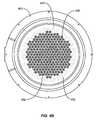
- FIG. 4Bis a bottom view of a showerhead 453 for use with a processing chamber according to disclosed embodiments.
- showerhead 453corresponds with the showerhead shown in FIG. 4A .
- Through-holes 456are depicted with a larger inner-diameter (ID) on the bottom of showerhead 453 and a smaller ID at the top. Small holes 455 are distributed substantially evenly over the surface of the showerhead, even amongst the through-holes 456 which helps to provide more even mixing than other embodiments described herein.
- IDinner-diameter
- An exemplary filmis created on a substrate supported by a pedestal (not shown) within substrate processing region 470 when plasma effluents arriving through through-holes 456 in showerhead 453 combine with a silicon-containing precursor arriving through the small holes 455 originating from hollow volumes 451 .
- substrate processing region 470may be equipped to support a plasma for other processes such as curing, no plasma is present during the growth of the exemplary film.
- a plasmamay be ignited either in chamber plasma region 420 above showerhead 453 or substrate processing region 470 below showerhead 453 .
- a plasmais present in chamber plasma region 420 to produce the excited plasma effluents from an inflow of an inert gas.
- An AC voltage typically in the radio frequency (RF) rangeis applied between the conductive top portion 421 of the processing chamber and showerhead 453 to ignite a plasma in chamber plasma region 420 during deposition.
- An RF power supplygenerates a high RF frequency of 13.56 MHz but may also generate other frequencies alone or in combination with the 13.56 MHz frequency.
- flowable filmsmay be produced using plasma powers below 1000 Watts, below 700 Watts, below 600 Watts or below 500 Watts in different embodiments.
- Conformal filmsmay be produced using plasma densities above or about 1000 Watts, above or about 1300 Watts, above or about 1700 Watts or above or about 200 Watts in different embodiments.
- the plasma densityis varied from low to high, for example, the transition from flowable to conformal is smooth, not discrete.
- the plasma power(and other design parameters) may be varied to select a balance between the conformal and flowable properties of a particular film.
- Plasma power requirementsmay change when another inert gas or mixture is used or another frequency is selected to excite the capacitive plasma.
- Plasma densitiesare necessary in the RPS 410 (when no plasma is struck in chamber plasma region 420 ) since the plasma effluents must travel a greater distance which provides more opportunity for deexcitation.
- Plasma densitiesalso require adjustment as the diameters of through-holes 456 are modified. Larger through-holes 456 conduct plasma effluents with less deexcitation so plasma powers may be reduced. Smaller through-holes 456 offer greater protection against undesirable plasma-excitation of the carbon-free silicon-and-nitrogen-containing precursor but require greater power densities either in chamber plasma region 420 or in RPS 410 .
- the top plasmamay be left at low or no power when the bottom plasma in the substrate processing region 470 is turned on to either cure a film or clean the interior surfaces bordering substrate processing region 470 .
- a plasma in substrate processing region 470is ignited by applying an AC voltage between showerhead 453 and the pedestal or bottom of the chamber.
- a cleaning gasmay be introduced into substrate processing region 470 while the plasma is present.
- the pedestalmay have a heat exchange channel through which a heat exchange fluid flows to control the temperature of the substrate.
- the heat exchange fluidmay comprise ethylene glycol and water.
- the wafer support platter of the pedestal(preferably aluminum, ceramic, or a combination thereof) may also be resistively heated in order to achieve relatively high temperatures (from about 120° C. through about 1100° C.) using an embedded single-loop embedded heater element configured to make two full turns in the form of parallel concentric circles.
- An outer portion of the heater elementmay run adjacent to a perimeter of the support platter, while an inner portion runs on the path of a concentric circle having a smaller radius.
- the wiring to the heater elementpasses through the stem of the pedestal.
- the substrate processing systemis controlled by a system controller.
- the system controllerincludes a hard disk drive, a floppy disk drive and a processor.
- the processorcontains a single-board computer (SBC), analog and digital input/output boards, interface boards and stepper motor controller boards.
- SBCsingle-board computer
- Various parts of CVD systemconform to the Versa Modular European (VME) standard which defines board, card cage, and connector dimensions and types.
- VMEVersa Modular European
- the VME standardalso defines the bus structure as having a 16-bit data bus and a 24-bit address bus.
- the system controllercontrols all of the activities of the CVD machine.
- the system controllerexecutes system control software, which is a computer program stored in a computer-readable medium.
- the mediumis a hard disk drive, but the medium may also be other kinds of memory.
- the computer programincludes sets of instructions that dictate the timing, mixture of gases, chamber pressure, chamber temperature, RF power levels, susceptor position, and other parameters of a particular process.
- Other computer programs stored on other memory devicesincluding, for example, a floppy disk or other another appropriate drive, may also be used to instruct the system controller.
- a process for depositing a film stack on a substrate or a process for cleaning a chambercan be implemented using a computer program product that is executed by the system controller.
- the computer program codecan be written in any conventional computer readable programming language: for example, 68000 assembly language, C, C++, Pascal, Fortran or others.
- Suitable program codeis entered into a single file, or multiple files, using a conventional text editor, and stored or embodied in a computer usable medium, such as a memory system of the computer. If the entered code text is in a high level language, the code is compiled, and the resultant compiler code is then linked with an object code of precompiled Microsoft Windows® library routines. To execute the linked, compiled object code the system user invokes the object code, causing the computer system to load the code in memory. The CPU then reads and executes the code to perform the tasks identified in the program.
- the interface between a user and the controlleris via a flat-panel touch-sensitive monitor.
- two monitorsare used, one mounted in the clean room wall for the operators and the other behind the wall for the service technicians.
- the two monitorsmay simultaneously display the same information, in which case only one accepts input at a time.
- the operatortouches a designated area of the touch-sensitive monitor.
- the touched areachanges its highlighted color, or a new menu or screen is displayed, confirming communication between the operator and the touch-sensitive monitor.
- Other devicessuch as a keyboard, mouse, or other pointing or communication device, may be used instead of or in addition to the touch-sensitive monitor to allow the user to communicate with the system controller.
- substratemay be a support substrate with or without layers formed thereon.
- the support substratemay be an insulator or a semiconductor of a variety of doping concentrations and profiles and may, for example, be a semiconductor substrate of the type used in the manufacture of integrated circuits.
- a layer of “silicon oxide”is used as a shorthand for and interchangeably with a silicon-and-oxygen-containing material.
- silicon oxidemay include concentrations of other elemental constituents such as nitrogen, hydrogen, carbon and the like.
- silicon oxideconsists essentially of silicon and oxygen.
- precursoris used to refer to any process gas which takes part in a reaction to either remove material from or deposit material onto a surface.
- a gas in an “excited state”describes a gas wherein at least some of the gas molecules are in vibrationally-excited, dissociated and/or ionized states.
- a “gas”may be a combination of two or more gases and may include substances which are normally liquid or solid but temporarily carried along with other “carrier gases.”
- a “radical precursor”is used to describe plasma effluents (a gas in an excited state which is exiting a plasma) which participate in a reaction to either remove material from or deposit material on a surface.
- a “radical-nitrogen precursor”is a radical precursor which contains nitrogen and a “radical-hydrogen precursor” is a radical precursor which contains hydrogen.
- inert gasrefers to any gas which does not form chemical bonds when etching or being incorporated into a film.
- exemplary inert gasesinclude noble gases but may include other gases so long as no chemical bonds are formed when (typically) trace amounts are trapped in a film.
- trenchis used throughout with no implication that the etched geometry has a large horizontal aspect ratio. Viewed from above the surface, trenches may appear circular, oval, polygonal, rectangular, or a variety of other shapes.
- viais used to refer to a low aspect ratio trench (as viewed from above) which may or may not be filled with metal to form a vertical electrical connection.
- a “conformal” layerrefers to a generally uniform layer of material on a surface in the same shape as the surface, i.e., the surface of the layer and the surface being covered are generally parallel.
- the deposited materiallikely cannot be 100% conformal and thus the term “generally” allows for acceptable tolerances.
Landscapes
- Chemical & Material Sciences (AREA)
- Engineering & Computer Science (AREA)
- Physics & Mathematics (AREA)
- Power Engineering (AREA)
- Chemical Kinetics & Catalysis (AREA)
- Condensed Matter Physics & Semiconductors (AREA)
- General Physics & Mathematics (AREA)
- Manufacturing & Machinery (AREA)
- Computer Hardware Design (AREA)
- Microelectronics & Electronic Packaging (AREA)
- General Chemical & Material Sciences (AREA)
- Materials Engineering (AREA)
- Mechanical Engineering (AREA)
- Metallurgy (AREA)
- Organic Chemistry (AREA)
- Plasma & Fusion (AREA)
- Analytical Chemistry (AREA)
- Inorganic Chemistry (AREA)
- Chemical Vapour Deposition (AREA)
- Formation Of Insulating Films (AREA)
Abstract
Description
Claims (13)
Priority Applications (3)
| Application Number | Priority Date | Filing Date | Title |
|---|---|---|---|
| US12/874,886US8329262B2 (en) | 2010-01-05 | 2010-09-02 | Dielectric film formation using inert gas excitation |
| PCT/US2010/060593WO2011084532A2 (en) | 2010-01-05 | 2010-12-15 | Dielectric film formation using inert gas excitation |
| TW099144277ATW201127983A (en) | 2010-01-05 | 2010-12-16 | Dielectric film formation using inert gas excitation |
Applications Claiming Priority (2)
| Application Number | Priority Date | Filing Date | Title |
|---|---|---|---|
| US29220310P | 2010-01-05 | 2010-01-05 | |
| US12/874,886US8329262B2 (en) | 2010-01-05 | 2010-09-02 | Dielectric film formation using inert gas excitation |
Publications (2)
| Publication Number | Publication Date |
|---|---|
| US20110165347A1 US20110165347A1 (en) | 2011-07-07 |
| US8329262B2true US8329262B2 (en) | 2012-12-11 |
Family
ID=44224852
Family Applications (1)
| Application Number | Title | Priority Date | Filing Date |
|---|---|---|---|
| US12/874,886Expired - Fee RelatedUS8329262B2 (en) | 2010-01-05 | 2010-09-02 | Dielectric film formation using inert gas excitation |
Country Status (3)
| Country | Link |
|---|---|
| US (1) | US8329262B2 (en) |
| TW (1) | TW201127983A (en) |
| WO (1) | WO2011084532A2 (en) |
Cited By (82)
| Publication number | Priority date | Publication date | Assignee | Title |
|---|---|---|---|---|
| US20170229328A1 (en)* | 2015-08-06 | 2017-08-10 | Applied Materials, Inc. | Bolted wafer chuck thermal management systems and methods for wafer processing systems |
| US9887080B2 (en) | 2015-12-28 | 2018-02-06 | Samsung Electronics Co., Ltd. | Method of forming SiOCN material layer and method of fabricating semiconductor device |
| US9947549B1 (en) | 2016-10-10 | 2018-04-17 | Applied Materials, Inc. | Cobalt-containing material removal |
| US9966240B2 (en) | 2014-10-14 | 2018-05-08 | Applied Materials, Inc. | Systems and methods for internal surface conditioning assessment in plasma processing equipment |
| US9978564B2 (en) | 2012-09-21 | 2018-05-22 | Applied Materials, Inc. | Chemical control features in wafer process equipment |
| US10026621B2 (en) | 2016-11-14 | 2018-07-17 | Applied Materials, Inc. | SiN spacer profile patterning |
| US10032606B2 (en) | 2012-08-02 | 2018-07-24 | Applied Materials, Inc. | Semiconductor processing with DC assisted RF power for improved control |
| US10043684B1 (en) | 2017-02-06 | 2018-08-07 | Applied Materials, Inc. | Self-limiting atomic thermal etching systems and methods |
| US10043674B1 (en) | 2017-08-04 | 2018-08-07 | Applied Materials, Inc. | Germanium etching systems and methods |
| US10049891B1 (en) | 2017-05-31 | 2018-08-14 | Applied Materials, Inc. | Selective in situ cobalt residue removal |
| US10062585B2 (en) | 2016-10-04 | 2018-08-28 | Applied Materials, Inc. | Oxygen compatible plasma source |
| US10062575B2 (en) | 2016-09-09 | 2018-08-28 | Applied Materials, Inc. | Poly directional etch by oxidation |
| US10128086B1 (en) | 2017-10-24 | 2018-11-13 | Applied Materials, Inc. | Silicon pretreatment for nitride removal |
| US10163696B2 (en) | 2016-11-11 | 2018-12-25 | Applied Materials, Inc. | Selective cobalt removal for bottom up gapfill |
| US10170336B1 (en) | 2017-08-04 | 2019-01-01 | Applied Materials, Inc. | Methods for anisotropic control of selective silicon removal |
| US10186428B2 (en) | 2016-11-11 | 2019-01-22 | Applied Materials, Inc. | Removal methods for high aspect ratio structures |
| US10224180B2 (en) | 2016-10-04 | 2019-03-05 | Applied Materials, Inc. | Chamber with flow-through source |
| US10224210B2 (en) | 2014-12-09 | 2019-03-05 | Applied Materials, Inc. | Plasma processing system with direct outlet toroidal plasma source |
| US10242908B2 (en) | 2016-11-14 | 2019-03-26 | Applied Materials, Inc. | Airgap formation with damage-free copper |
| US10256112B1 (en) | 2017-12-08 | 2019-04-09 | Applied Materials, Inc. | Selective tungsten removal |
| US10256079B2 (en) | 2013-02-08 | 2019-04-09 | Applied Materials, Inc. | Semiconductor processing systems having multiple plasma configurations |
| US10283321B2 (en) | 2011-01-18 | 2019-05-07 | Applied Materials, Inc. | Semiconductor processing system and methods using capacitively coupled plasma |
| US10283324B1 (en) | 2017-10-24 | 2019-05-07 | Applied Materials, Inc. | Oxygen treatment for nitride etching |
| US10297458B2 (en) | 2017-08-07 | 2019-05-21 | Applied Materials, Inc. | Process window widening using coated parts in plasma etch processes |
| US10319649B2 (en) | 2017-04-11 | 2019-06-11 | Applied Materials, Inc. | Optical emission spectroscopy (OES) for remote plasma monitoring |
| US10319600B1 (en) | 2018-03-12 | 2019-06-11 | Applied Materials, Inc. | Thermal silicon etch |
| US10319739B2 (en) | 2017-02-08 | 2019-06-11 | Applied Materials, Inc. | Accommodating imperfectly aligned memory holes |
| US10319603B2 (en) | 2016-10-07 | 2019-06-11 | Applied Materials, Inc. | Selective SiN lateral recess |
| US10354889B2 (en) | 2017-07-17 | 2019-07-16 | Applied Materials, Inc. | Non-halogen etching of silicon-containing materials |
| US10403507B2 (en) | 2017-02-03 | 2019-09-03 | Applied Materials, Inc. | Shaped etch profile with oxidation |
| US10424463B2 (en) | 2015-08-07 | 2019-09-24 | Applied Materials, Inc. | Oxide etch selectivity systems and methods |
| US10424485B2 (en) | 2013-03-01 | 2019-09-24 | Applied Materials, Inc. | Enhanced etching processes using remote plasma sources |
| US10424487B2 (en) | 2017-10-24 | 2019-09-24 | Applied Materials, Inc. | Atomic layer etching processes |
| US10431429B2 (en) | 2017-02-03 | 2019-10-01 | Applied Materials, Inc. | Systems and methods for radial and azimuthal control of plasma uniformity |
| US10465294B2 (en) | 2014-05-28 | 2019-11-05 | Applied Materials, Inc. | Oxide and metal removal |
| US10468285B2 (en) | 2015-02-03 | 2019-11-05 | Applied Materials, Inc. | High temperature chuck for plasma processing systems |
| US10468276B2 (en) | 2015-08-06 | 2019-11-05 | Applied Materials, Inc. | Thermal management systems and methods for wafer processing systems |
| US10468267B2 (en) | 2017-05-31 | 2019-11-05 | Applied Materials, Inc. | Water-free etching methods |
| US10490406B2 (en) | 2018-04-10 | 2019-11-26 | Appled Materials, Inc. | Systems and methods for material breakthrough |
| US10497573B2 (en) | 2018-03-13 | 2019-12-03 | Applied Materials, Inc. | Selective atomic layer etching of semiconductor materials |
| US10504754B2 (en) | 2016-05-19 | 2019-12-10 | Applied Materials, Inc. | Systems and methods for improved semiconductor etching and component protection |
| US10504700B2 (en) | 2015-08-27 | 2019-12-10 | Applied Materials, Inc. | Plasma etching systems and methods with secondary plasma injection |
| US10522371B2 (en) | 2016-05-19 | 2019-12-31 | Applied Materials, Inc. | Systems and methods for improved semiconductor etching and component protection |
| US10541184B2 (en) | 2017-07-11 | 2020-01-21 | Applied Materials, Inc. | Optical emission spectroscopic techniques for monitoring etching |
| US10541246B2 (en) | 2017-06-26 | 2020-01-21 | Applied Materials, Inc. | 3D flash memory cells which discourage cross-cell electrical tunneling |
| US10546729B2 (en) | 2016-10-04 | 2020-01-28 | Applied Materials, Inc. | Dual-channel showerhead with improved profile |
| US10566206B2 (en) | 2016-12-27 | 2020-02-18 | Applied Materials, Inc. | Systems and methods for anisotropic material breakthrough |
| US10573527B2 (en) | 2018-04-06 | 2020-02-25 | Applied Materials, Inc. | Gas-phase selective etching systems and methods |
| US10573496B2 (en) | 2014-12-09 | 2020-02-25 | Applied Materials, Inc. | Direct outlet toroidal plasma source |
| US10593560B2 (en) | 2018-03-01 | 2020-03-17 | Applied Materials, Inc. | Magnetic induction plasma source for semiconductor processes and equipment |
| US10593523B2 (en) | 2014-10-14 | 2020-03-17 | Applied Materials, Inc. | Systems and methods for internal surface conditioning in plasma processing equipment |
| US10615047B2 (en) | 2018-02-28 | 2020-04-07 | Applied Materials, Inc. | Systems and methods to form airgaps |
| US10629473B2 (en) | 2016-09-09 | 2020-04-21 | Applied Materials, Inc. | Footing removal for nitride spacer |
| US10672642B2 (en) | 2018-07-24 | 2020-06-02 | Applied Materials, Inc. | Systems and methods for pedestal configuration |
| US10679870B2 (en) | 2018-02-15 | 2020-06-09 | Applied Materials, Inc. | Semiconductor processing chamber multistage mixing apparatus |
| US10699879B2 (en) | 2018-04-17 | 2020-06-30 | Applied Materials, Inc. | Two piece electrode assembly with gap for plasma control |
| US10727080B2 (en) | 2017-07-07 | 2020-07-28 | Applied Materials, Inc. | Tantalum-containing material removal |
| US10755941B2 (en) | 2018-07-06 | 2020-08-25 | Applied Materials, Inc. | Self-limiting selective etching systems and methods |
| US10854426B2 (en) | 2018-01-08 | 2020-12-01 | Applied Materials, Inc. | Metal recess for semiconductor structures |
| US10872778B2 (en) | 2018-07-06 | 2020-12-22 | Applied Materials, Inc. | Systems and methods utilizing solid-phase etchants |
| US10886137B2 (en) | 2018-04-30 | 2021-01-05 | Applied Materials, Inc. | Selective nitride removal |
| US10892198B2 (en) | 2018-09-14 | 2021-01-12 | Applied Materials, Inc. | Systems and methods for improved performance in semiconductor processing |
| US10903054B2 (en) | 2017-12-19 | 2021-01-26 | Applied Materials, Inc. | Multi-zone gas distribution systems and methods |
| US10920320B2 (en) | 2017-06-16 | 2021-02-16 | Applied Materials, Inc. | Plasma health determination in semiconductor substrate processing reactors |
| US10920319B2 (en) | 2019-01-11 | 2021-02-16 | Applied Materials, Inc. | Ceramic showerheads with conductive electrodes |
| US10943834B2 (en) | 2017-03-13 | 2021-03-09 | Applied Materials, Inc. | Replacement contact process |
| US10964512B2 (en) | 2018-02-15 | 2021-03-30 | Applied Materials, Inc. | Semiconductor processing chamber multistage mixing apparatus and methods |
| US11049755B2 (en) | 2018-09-14 | 2021-06-29 | Applied Materials, Inc. | Semiconductor substrate supports with embedded RF shield |
| US11062887B2 (en) | 2018-09-17 | 2021-07-13 | Applied Materials, Inc. | High temperature RF heater pedestals |
| US11121002B2 (en) | 2018-10-24 | 2021-09-14 | Applied Materials, Inc. | Systems and methods for etching metals and metal derivatives |
| US11239061B2 (en) | 2014-11-26 | 2022-02-01 | Applied Materials, Inc. | Methods and systems to enhance process uniformity |
| US11257693B2 (en) | 2015-01-09 | 2022-02-22 | Applied Materials, Inc. | Methods and systems to improve pedestal temperature control |
| US11276559B2 (en) | 2017-05-17 | 2022-03-15 | Applied Materials, Inc. | Semiconductor processing chamber for multiple precursor flow |
| US11276590B2 (en) | 2017-05-17 | 2022-03-15 | Applied Materials, Inc. | Multi-zone semiconductor substrate supports |
| US11328909B2 (en) | 2017-12-22 | 2022-05-10 | Applied Materials, Inc. | Chamber conditioning and removal processes |
| US11417534B2 (en) | 2018-09-21 | 2022-08-16 | Applied Materials, Inc. | Selective material removal |
| US11437242B2 (en) | 2018-11-27 | 2022-09-06 | Applied Materials, Inc. | Selective removal of silicon-containing materials |
| US11594428B2 (en) | 2015-02-03 | 2023-02-28 | Applied Materials, Inc. | Low temperature chuck for plasma processing systems |
| US11682560B2 (en) | 2018-10-11 | 2023-06-20 | Applied Materials, Inc. | Systems and methods for hafnium-containing film removal |
| US11721527B2 (en) | 2019-01-07 | 2023-08-08 | Applied Materials, Inc. | Processing chamber mixing systems |
| US12057329B2 (en) | 2016-06-29 | 2024-08-06 | Applied Materials, Inc. | Selective etch using material modification and RF pulsing |
| US12340979B2 (en) | 2017-05-17 | 2025-06-24 | Applied Materials, Inc. | Semiconductor processing chamber for improved precursor flow |
Families Citing this family (42)
| Publication number | Priority date | Publication date | Assignee | Title |
|---|---|---|---|---|
| US8232176B2 (en) | 2006-06-22 | 2012-07-31 | Applied Materials, Inc. | Dielectric deposition and etch back processes for bottom up gapfill |
| US7867923B2 (en)* | 2007-10-22 | 2011-01-11 | Applied Materials, Inc. | High quality silicon oxide films by remote plasma CVD from disilane precursors |
| US8357435B2 (en) | 2008-05-09 | 2013-01-22 | Applied Materials, Inc. | Flowable dielectric equipment and processes |
| US8980382B2 (en) | 2009-12-02 | 2015-03-17 | Applied Materials, Inc. | Oxygen-doping for non-carbon radical-component CVD films |
| US8741788B2 (en) | 2009-08-06 | 2014-06-03 | Applied Materials, Inc. | Formation of silicon oxide using non-carbon flowable CVD processes |
| US8449942B2 (en) | 2009-11-12 | 2013-05-28 | Applied Materials, Inc. | Methods of curing non-carbon flowable CVD films |
| JP2013516763A (en) | 2009-12-30 | 2013-05-13 | アプライド マテリアルズ インコーポレイテッド | Dielectric film growth using radicals generated using a flexible nitrogen / hydrogen ratio |
| SG182336A1 (en) | 2010-01-06 | 2012-08-30 | Applied Materials Inc | Flowable dielectric using oxide liner |
| KR101837648B1 (en) | 2010-01-07 | 2018-04-19 | 어플라이드 머티어리얼스, 인코포레이티드 | Insitu ozone cure for radicalcomponent cvd |
| JP2013521650A (en) | 2010-03-05 | 2013-06-10 | アプライド マテリアルズ インコーポレイテッド | Conformal layer by radical component CVD |
| US9324576B2 (en) | 2010-05-27 | 2016-04-26 | Applied Materials, Inc. | Selective etch for silicon films |
| US9285168B2 (en) | 2010-10-05 | 2016-03-15 | Applied Materials, Inc. | Module for ozone cure and post-cure moisture treatment |
| US8664127B2 (en) | 2010-10-15 | 2014-03-04 | Applied Materials, Inc. | Two silicon-containing precursors for gapfill enhancing dielectric liner |
| US8450191B2 (en) | 2011-01-24 | 2013-05-28 | Applied Materials, Inc. | Polysilicon films by HDP-CVD |
| US8716154B2 (en) | 2011-03-04 | 2014-05-06 | Applied Materials, Inc. | Reduced pattern loading using silicon oxide multi-layers |
| US8999856B2 (en) | 2011-03-14 | 2015-04-07 | Applied Materials, Inc. | Methods for etch of sin films |
| US9064815B2 (en) | 2011-03-14 | 2015-06-23 | Applied Materials, Inc. | Methods for etch of metal and metal-oxide films |
| US8445078B2 (en) | 2011-04-20 | 2013-05-21 | Applied Materials, Inc. | Low temperature silicon oxide conversion |
| US8466073B2 (en) | 2011-06-03 | 2013-06-18 | Applied Materials, Inc. | Capping layer for reduced outgassing |
| US9404178B2 (en) | 2011-07-15 | 2016-08-02 | Applied Materials, Inc. | Surface treatment and deposition for reduced outgassing |
| US8617989B2 (en) | 2011-09-26 | 2013-12-31 | Applied Materials, Inc. | Liner property improvement |
| US8551891B2 (en) | 2011-10-04 | 2013-10-08 | Applied Materials, Inc. | Remote plasma burn-in |
| US9267739B2 (en) | 2012-07-18 | 2016-02-23 | Applied Materials, Inc. | Pedestal with multi-zone temperature control and multiple purge capabilities |
| US8889566B2 (en) | 2012-09-11 | 2014-11-18 | Applied Materials, Inc. | Low cost flowable dielectric films |
| US9023734B2 (en)* | 2012-09-18 | 2015-05-05 | Applied Materials, Inc. | Radical-component oxide etch |
| US20140099794A1 (en)* | 2012-09-21 | 2014-04-10 | Applied Materials, Inc. | Radical chemistry modulation and control using multiple flow pathways |
| US9018108B2 (en) | 2013-01-25 | 2015-04-28 | Applied Materials, Inc. | Low shrinkage dielectric films |
| US9773648B2 (en) | 2013-08-30 | 2017-09-26 | Applied Materials, Inc. | Dual discharge modes operation for remote plasma |
| US20150200094A1 (en)* | 2014-01-10 | 2015-07-16 | Applied Materials, Inc. | Carbon film stress relaxation |
| US9299537B2 (en) | 2014-03-20 | 2016-03-29 | Applied Materials, Inc. | Radial waveguide systems and methods for post-match control of microwaves |
| US9903020B2 (en) | 2014-03-31 | 2018-02-27 | Applied Materials, Inc. | Generation of compact alumina passivation layers on aluminum plasma equipment components |
| US9412581B2 (en) | 2014-07-16 | 2016-08-09 | Applied Materials, Inc. | Low-K dielectric gapfill by flowable deposition |
| US9496167B2 (en) | 2014-07-31 | 2016-11-15 | Applied Materials, Inc. | Integrated bit-line airgap formation and gate stack post clean |
| US9613822B2 (en) | 2014-09-25 | 2017-04-04 | Applied Materials, Inc. | Oxide etch selectivity enhancement |
| US9881805B2 (en) | 2015-03-02 | 2018-01-30 | Applied Materials, Inc. | Silicon selective removal |
| US9922840B2 (en) | 2015-07-07 | 2018-03-20 | Applied Materials, Inc. | Adjustable remote dissociation |
| EP3942088A4 (en)* | 2019-03-22 | 2022-12-21 | Applied Materials, Inc. | METHOD AND DEVICE FOR THE DEPOSITION OF METAL NITRIDE |
| CN113614274A (en) | 2019-03-22 | 2021-11-05 | 应用材料公司 | Method and apparatus for depositing multilayer device with superconducting film |
| KR20210010816A (en)* | 2019-07-17 | 2021-01-28 | 에이에스엠 아이피 홀딩 비.브이. | Radical assist ignition plasma system and method |
| TWI753759B (en) | 2020-02-03 | 2022-01-21 | 美商應用材料股份有限公司 | Snspd with integrated aluminum nitride seed or waveguide layer |
| TWI780579B (en) | 2020-02-03 | 2022-10-11 | 美商應用材料股份有限公司 | Snspd with integrated aluminum nitride seed or waveguide layer |
| US20240332028A1 (en)* | 2023-03-29 | 2024-10-03 | Applied Materials, Inc. | Compressive films for large area gapfill |
Citations (303)
| Publication number | Priority date | Publication date | Assignee | Title |
|---|---|---|---|---|
| US4147571A (en) | 1977-07-11 | 1979-04-03 | Hewlett-Packard Company | Method for vapor epitaxial deposition of III/V materials utilizing organometallic compounds and a halogen or halide in a hot wall system |
| US4200666A (en)* | 1978-08-02 | 1980-04-29 | Texas Instruments Incorporated | Single component monomer for silicon nitride deposition |
| US4816098A (en) | 1987-07-16 | 1989-03-28 | Texas Instruments Incorporated | Apparatus for transferring workpieces |
| US4818326A (en) | 1987-07-16 | 1989-04-04 | Texas Instruments Incorporated | Processing apparatus |
| US4931354A (en) | 1987-11-02 | 1990-06-05 | Murata Manufacturing Co., Ltd. | Multilayer printed circuit board |
| US4946593A (en) | 1987-03-31 | 1990-08-07 | Acushnet Company | Rubber composition for use with potable water |
| US5016332A (en) | 1990-04-13 | 1991-05-21 | Branson International Plasma Corporation | Plasma reactor and process with wafer temperature control |
| US5110407A (en) | 1990-03-07 | 1992-05-05 | Hitachi, Ltd. | Surface fabricating device |
| US5271972A (en) | 1992-08-17 | 1993-12-21 | Applied Materials, Inc. | Method for depositing ozone/TEOS silicon oxide films of reduced surface sensitivity |
| US5279784A (en) | 1992-05-05 | 1994-01-18 | Bandag Licensing Corporation | Method of fabrication of composite tire thread |
| US5393708A (en) | 1992-10-08 | 1995-02-28 | Industrial Technology Research Institute | Inter-metal-dielectric planarization process |
| US5426076A (en) | 1991-07-16 | 1995-06-20 | Intel Corporation | Dielectric deposition and cleaning process for improved gap filling and device planarization |
| US5468687A (en) | 1994-07-27 | 1995-11-21 | International Business Machines Corporation | Method of making TA2 O5 thin film by low temperature ozone plasma annealing (oxidation) |
| US5485420A (en)* | 1992-12-11 | 1996-01-16 | Motorola, Inc. | Static-random-access memory cell and an integrated circuit having a static-random-access memory cell |
| US5530293A (en) | 1994-11-28 | 1996-06-25 | International Business Machines Corporation | Carbon-free hydrogen silsesquioxane with dielectric constant less than 3.2 annealed in hydrogen for integrated circuits |
| US5547703A (en) | 1994-04-11 | 1996-08-20 | Dow Corning Corporation | Method of forming si-o containing coatings |
| US5558717A (en) | 1994-11-30 | 1996-09-24 | Applied Materials | CVD Processing chamber |
| US5578532A (en) | 1990-07-16 | 1996-11-26 | Novellus Systems, Inc. | Wafer surface protection in a gas deposition process |
| US5587014A (en) | 1993-12-22 | 1996-12-24 | Sumitomo Chemical Company, Limited | Method for manufacturing group III-V compound semiconductor crystals |
| US5593741A (en) | 1992-11-30 | 1997-01-14 | Nec Corporation | Method and apparatus for forming silicon oxide film by chemical vapor deposition |
| US5620525A (en) | 1990-07-16 | 1997-04-15 | Novellus Systems, Inc. | Apparatus for supporting a substrate and introducing gas flow doximate to an edge of the substrate |
| US5622784A (en) | 1986-01-21 | 1997-04-22 | Seiko Epson Corporation | Synthetic resin ophthalmic lens having an inorganic coating |
| US5635409A (en) | 1991-05-20 | 1997-06-03 | Texas Instruments Incorporated | Real-time multi-zone semiconductor wafer temperature and process uniformity control system |
| DE19654737A1 (en) | 1995-12-28 | 1997-07-03 | Toshiba Kawasaki Kk | Semiconductor device for LSI devices |
| US5665643A (en) | 1994-11-15 | 1997-09-09 | Fujitsu Limited | Manufacture of planarized insulating layer |
| US5691009A (en) | 1994-11-08 | 1997-11-25 | Micron Technology, Inc. | Method of reducing carbon incorporation into films produced by chemical vapor deposition involving organic precursor compounds |
| US5769951A (en) | 1990-07-16 | 1998-06-23 | Novellus Systems Inc | Exclusion guard and gas-based substrate protection for chemical vapor deposition apparatus |
| US5786263A (en) | 1995-04-04 | 1998-07-28 | Motorola, Inc. | Method for forming a trench isolation structure in an integrated circuit |
| US5811325A (en) | 1996-12-31 | 1998-09-22 | Industrial Technology Research Institute | Method of making a polysilicon carbon source/drain heterojunction thin-film transistor |
| EP0892083A1 (en) | 1997-07-02 | 1999-01-20 | Applied Materials, Inc. | Method and apparatus for seasoning a substrate processing chamber |
| US5935340A (en) | 1996-11-13 | 1999-08-10 | Applied Materials, Inc. | Method and apparatus for gettering fluorine from chamber material surfaces |
| US5937308A (en) | 1997-03-26 | 1999-08-10 | Advanced Micro Devices, Inc. | Semiconductor trench isolation structure formed substantially within a single chamber |
| US5937323A (en) | 1997-06-03 | 1999-08-10 | Applied Materials, Inc. | Sequencing of the recipe steps for the optimal low-k HDP-CVD processing |
| US6008515A (en) | 1996-08-23 | 1999-12-28 | Mosel Vitelic, Inc. | Stacked capacitor having improved charge storage capacity |
| US6009830A (en) | 1997-11-21 | 2000-01-04 | Applied Materials Inc. | Independent gas feeds in a plasma reactor |
| US6014979A (en) | 1998-06-22 | 2000-01-18 | Applied Materials, Inc. | Localizing cleaning plasma for semiconductor processing |
| US6017791A (en)* | 1997-11-10 | 2000-01-25 | Taiwan Semiconductor Manufacturing Company | Multi-layer silicon nitride deposition method for forming low oxidation temperature thermally oxidized silicon nitride/silicon oxide (no) layer |
| US6024044A (en) | 1997-10-09 | 2000-02-15 | Applied Komatsu Technology, Inc. | Dual frequency excitation of plasma for film deposition |
| US6087243A (en) | 1997-10-21 | 2000-07-11 | Advanced Micro Devices, Inc. | Method of forming trench isolation with high integrity, ultra thin gate oxide |
| US6090723A (en) | 1997-02-10 | 2000-07-18 | Micron Technology, Inc. | Conditioning of dielectric materials |
| US6090442A (en) | 1997-04-14 | 2000-07-18 | University Technology Corporation | Method of growing films on substrates at room temperatures using catalyzed binary reaction sequence chemistry |
| US6114219A (en) | 1997-09-15 | 2000-09-05 | Advanced Micro Devices, Inc. | Method of manufacturing an isolation region in a semiconductor device using a flowable oxide-generating material |
| US6121130A (en) | 1998-11-16 | 2000-09-19 | Chartered Semiconductor Manufacturing Ltd. | Laser curing of spin-on dielectric thin films |
| US6140242A (en) | 1997-12-01 | 2000-10-31 | Samsung Electronics Co., Ltd. | Method of forming an isolation trench in a semiconductor device including annealing at an increased temperature |
| US6146970A (en) | 1998-05-26 | 2000-11-14 | Motorola Inc. | Capped shallow trench isolation and method of formation |
| US6156394A (en) | 1998-04-17 | 2000-12-05 | Optical Coating Laboratory, Inc. | Polymeric optical substrate method of treatment |
| US6156581A (en) | 1994-01-27 | 2000-12-05 | Advanced Technology Materials, Inc. | GaN-based devices using (Ga, AL, In)N base layers |
| US6165834A (en) | 1998-05-07 | 2000-12-26 | Micron Technology, Inc. | Method of forming capacitors, method of processing dielectric layers, method of forming a DRAM cell |
| US6180490B1 (en) | 1999-05-25 | 2001-01-30 | Chartered Semiconductor Manufacturing Ltd. | Method of filling shallow trenches |
| US6187682B1 (en) | 1998-05-26 | 2001-02-13 | Motorola Inc. | Inert plasma gas surface cleaning process performed insitu with physical vapor deposition (PVD) of a layer of material |
| US6207587B1 (en) | 1997-06-24 | 2001-03-27 | Micron Technology, Inc. | Method for forming a dielectric |
| JP2001148382A (en) | 1999-06-22 | 2001-05-29 | Applied Materials Inc | Formation of Liquid Silica Layer by Reaction of Organosilicon Compound and Hydroxyl-Forming Compound |
| US6287962B1 (en) | 2000-11-30 | 2001-09-11 | Taiwan Semiconductor Manufacturing Company | Method for making a novel graded silicon nitride/silicon oxide (SNO) hard mask for improved deep sub-micrometer semiconductor processing |
| US20010021595A1 (en) | 1998-10-30 | 2001-09-13 | Taiwan Semiconductor Manufacturing Company | Sub-atmospheric pressure thermal chemical vapor deposition (SACVD) trench isolation method with attenuated surface sensitivity |
| US20010029114A1 (en) | 2000-02-29 | 2001-10-11 | Michele Vulpio | Method of forming polymeric layers of silicon oxynitride |
| US6302964B1 (en) | 1998-06-16 | 2001-10-16 | Applied Materials, Inc. | One-piece dual gas faceplate for a showerhead in a semiconductor wafer processing system |
| US20010038919A1 (en) | 2000-03-20 | 2001-11-08 | Berry Ivan L. | Plasma curing process for porous silica thin film |
| US20010042511A1 (en) | 2000-05-12 | 2001-11-22 | Applied Materials, Inc. | Reduction of plasma edge effect on plasma enhanced CVD processes |
| US20010048980A1 (en) | 1997-11-20 | 2001-12-06 | Koji Kishimoto | High density plasma enhanced chemical vapor deposition method |
| US20010054387A1 (en) | 1996-11-14 | 2001-12-27 | Jonathan Frankel | Heater/lift assembly for high temperature processing chamber |
| US20010055889A1 (en) | 1997-04-17 | 2001-12-27 | Ravi Iyer | Method for improving thickness uniformity of deposited ozone-TEOS silicate glass layers |
| US20020048969A1 (en) | 2000-10-23 | 2002-04-25 | Applied Materials, Inc. | Method of forming film, method of manufacturing semiconductor device, and film forming apparatus |
| US6383954B1 (en) | 1999-07-27 | 2002-05-07 | Applied Materials, Inc. | Process gas distribution for forming stable fluorine-doped silicate glass and other films |
| US6387207B1 (en) | 2000-04-28 | 2002-05-14 | Applied Materials, Inc. | Integration of remote plasma generator with semiconductor processing chamber |
| US20020068466A1 (en) | 2000-12-06 | 2002-06-06 | Seung-Hwan Lee | Methods of forming thin films by atomic layer deposition |
| US20020068416A1 (en) | 2000-12-05 | 2002-06-06 | Chris Hsieh | Method for depositing an undopped silicate glass layer |
| US6406677B1 (en) | 1998-07-22 | 2002-06-18 | Eltron Research, Inc. | Methods for low and ambient temperature preparation of precursors of compounds of group III metals and group V elements |
| US20020081817A1 (en) | 2000-12-22 | 2002-06-27 | Jayendra Bhakta | Void reduction and increased throughput in trench fill processes |
| US20020079523A1 (en) | 2000-12-20 | 2002-06-27 | Micron Technology, Inc. | Reduction of damage in semiconductor container capacitors |
| US20020086166A1 (en) | 1998-08-27 | 2002-07-04 | Neil Hendricks | Silane-based nanoporous silica thin films and precursors for making same |
| US6448187B2 (en) | 1998-11-04 | 2002-09-10 | Applied Materials, Inc. | Method of improving moisture resistance of low dielectric constant films |
| US20020127350A1 (en) | 2001-03-07 | 2002-09-12 | Applied Materials, Inc. | High-permeability magnetic shield for improved process uniformity in nonmagnetized plasma process chambers |
| US20020129769A1 (en) | 2001-03-19 | 2002-09-19 | Apex Co. Ltd. | Chemical vapor deposition apparatus |
| US20020142585A1 (en) | 2000-01-18 | 2002-10-03 | Applied Materials, Inc. | Very low dielectric constant plasma-enhanced CVD films |
| WO2002077320A1 (en) | 2001-03-23 | 2002-10-03 | Dow Corning Corporation | Method for producing hydrogenated silicon oxycarbide films |
| US20020146879A1 (en) | 2001-04-10 | 2002-10-10 | Applied Materials, Inc. | Limiting Hydrogen ion diffusion using multiple layers of SiO2 and Si3N4 |
| US6469283B1 (en) | 1999-03-04 | 2002-10-22 | Applied Materials, Inc. | Method and apparatus for reducing thermal gradients within a substrate support |
| US20020164429A1 (en) | 2001-02-22 | 2002-11-07 | Applied Materials, Inc. | Methods for forming a low dielectric constant carbon-containing film, and films produced thereby |
| US20020164891A1 (en) | 2001-05-03 | 2002-11-07 | International Business Machines Corporation | Ordered two-phase dielectric film, and semiconductor device containing the same |
| US20020177298A1 (en) | 2001-03-13 | 2002-11-28 | Nobuo Konishi | Film forming method and film forming apparatus |
| US20020182893A1 (en) | 2001-06-05 | 2002-12-05 | International Business Machines Corporation | Oxidation of silicon nitride films in semiconductor devices |
| JP2002370059A (en) | 2001-03-13 | 2002-12-24 | Tokyo Electron Ltd | Film-forming method and film-forming device |
| US20030001201A1 (en)* | 2001-06-29 | 2003-01-02 | Mitsubishi Denki Kabushiki Kaisha | Semiconductor device and manufacturing method thereof |
| US6503557B1 (en) | 1997-02-10 | 2003-01-07 | Saint-Gobain Vitrage | Process for depositing at least one thin layer based on silicon nitride or oxynitride on a transparent substrate |
| US6506253B2 (en) | 2000-09-22 | 2003-01-14 | Tokyo Electron Limited | Photo-excited gas processing apparatus for semiconductor process |
| US6508879B1 (en) | 1999-11-12 | 2003-01-21 | Sony Corporation | Method of fabricating group III-V nitride compound semiconductor and method of fabricating semiconductor device |
| US6509283B1 (en) | 1998-05-13 | 2003-01-21 | National Semiconductor Corporation | Thermal oxidation method utilizing atomic oxygen to reduce dangling bonds in silicon dioxide grown on silicon |
| US20030023113A1 (en) | 2001-04-26 | 2003-01-30 | Atofina | Process for the manufacture of aqueous solutions of unsaturated quaternary ammonium salts |
| US6524931B1 (en) | 1999-07-20 | 2003-02-25 | Motorola, Inc. | Method for forming a trench isolation structure in an integrated circuit |
| US20030040199A1 (en) | 2000-12-07 | 2003-02-27 | Agarwal Vishnu K. | Photo-assisted remote plasma apparatus and method |
| US6528332B2 (en) | 2001-04-27 | 2003-03-04 | Advanced Micro Devices, Inc. | Method and system for reducing polymer build up during plasma etch of an intermetal dielectric |
| US20030064154A1 (en) | 2001-08-06 | 2003-04-03 | Laxman Ravi K. | Low-K dielectric thin films and chemical vapor deposition method of making same |
| US6544900B2 (en) | 1999-12-23 | 2003-04-08 | Asm America, Inc. | In situ dielectric stacks |
| US6548416B2 (en) | 2001-07-24 | 2003-04-15 | Axcelis Technolgoies, Inc. | Plasma ashing process |
| US6548899B2 (en) | 1999-06-11 | 2003-04-15 | Electron Vision Corporation | Method of processing films prior to chemical vapor deposition using electron beam processing |
| US20030077918A1 (en) | 2000-05-05 | 2003-04-24 | Hui-Jung Wu | Simplified method to produce nanoporous silicon-based films |
| US6559026B1 (en) | 2000-05-25 | 2003-05-06 | Applied Materials, Inc | Trench fill with HDP-CVD process including coupled high power density plasma deposition |
| US6566278B1 (en) | 2000-08-24 | 2003-05-20 | Applied Materials Inc. | Method for densification of CVD carbon-doped silicon oxide films through UV irradiation |
| US20030113992A1 (en) | 1998-02-11 | 2003-06-19 | Applied Materials, Inc. | Method of depositing a low dielectric with organo silane |
| US6583063B1 (en) | 1998-12-03 | 2003-06-24 | Applied Materials, Inc. | Plasma etching of silicon using fluorinated gas mixtures |
| US20030118748A1 (en) | 2001-12-25 | 2003-06-26 | Akira Kumagai | Silicon oxide film formation method |
| US20030124873A1 (en) | 2001-12-28 | 2003-07-03 | Guangcai Xing | Method of annealing an oxide film |
| US6589868B2 (en) | 2001-02-08 | 2003-07-08 | Applied Materials, Inc. | Si seasoning to reduce particles, extend clean frequency, block mobile ions and increase chamber throughput |
| US6596654B1 (en) | 2001-08-24 | 2003-07-22 | Novellus Systems, Inc. | Gap fill for high aspect ratio structures |
| US6599839B1 (en) | 2001-02-02 | 2003-07-29 | Advanced Micro Devices, Inc. | Plasma etch process for nonhomogenous film |
| US20030143841A1 (en) | 2002-01-26 | 2003-07-31 | Yang Michael X. | Integration of titanium and titanium nitride layers |
| US6602806B1 (en) | 1999-08-17 | 2003-08-05 | Applied Materials, Inc. | Thermal CVD process for depositing a low dielectric constant carbon-doped silicon oxide film |
| US20030159656A1 (en) | 2001-05-11 | 2003-08-28 | Applied Materials, Inc. | Hydrogen assisted undoped silicon oxide deposition process for HDP-CVD |
| US6614181B1 (en) | 2000-08-23 | 2003-09-02 | Applied Materials, Inc. | UV radiation source for densification of CVD carbon-doped silicon oxide films |
| US20030172872A1 (en) | 2002-01-25 | 2003-09-18 | Applied Materials, Inc. | Apparatus for cyclical deposition of thin films |
| US6624064B1 (en) | 1997-10-10 | 2003-09-23 | Applied Materials, Inc. | Chamber seasoning method to improve adhesion of F-containing dielectric film to metal for VLSI application |
| US6630413B2 (en) | 2000-04-28 | 2003-10-07 | Asm Japan K.K. | CVD syntheses of silicon nitride materials |
| US20030199151A1 (en) | 2002-04-18 | 2003-10-23 | Nanya Technology Corporation | Method of fabricating a shallow trench isolation structure |
| US6660391B1 (en) | 1998-04-28 | 2003-12-09 | Asml Us, Inc. | Low κ dielectric inorganic/organic hybrid films and method of making |
| US20030232495A1 (en) | 2002-05-08 | 2003-12-18 | Farhad Moghadam | Methods and apparatus for E-beam treatment used to fabricate integrated circuit devices |
| US6667553B2 (en) | 1998-05-29 | 2003-12-23 | Dow Corning Corporation | H:SiOC coated substrates |
| US6670284B2 (en) | 1998-06-10 | 2003-12-30 | Micron Technology, Inc. | Method of decontaminating process chambers, methods of reducing defects in anti-reflective coatings, and resulting semiconductor structures |
| US6676751B2 (en) | 1999-05-07 | 2004-01-13 | Cbl Technologies, Inc | Epitaxial film produced by sequential hydride vapor phase epitaxy |
| US20040008334A1 (en) | 2002-07-11 | 2004-01-15 | Sreenivasan Sidlgata V. | Step and repeat imprint lithography systems |
| US6682659B1 (en)* | 1999-11-08 | 2004-01-27 | Taiwan Semiconductor Manufacturing Company | Method for forming corrosion inhibited conductor layer |
| US6682969B1 (en) | 2000-08-31 | 2004-01-27 | Micron Technology, Inc. | Top electrode in a strongly oxidizing environment |
| US6683364B2 (en) | 2001-07-13 | 2004-01-27 | Samsung Electronics Co., Ltd. | Integrated circuit devices including an isolation region defining an active region area and methods for manufacturing the same |
| US20040020601A1 (en) | 2000-02-10 | 2004-02-05 | Applied Materials, Inc. | Process and an integrated tool for low k dielectric deposition including a pecvd capping module |
| US20040029353A1 (en) | 2002-08-06 | 2004-02-12 | Chartered Semiconductor Manufacturing Ltd. | Method of forming a shallow trench isolation structure featuring a group of insulator liner layers located on the surfaces of a shallow trench shape |
| US20040029352A1 (en) | 2002-08-07 | 2004-02-12 | International Business Machines Corporation | Triple oxide fill for trench isolation |
| US20040048492A1 (en) | 2001-01-26 | 2004-03-11 | Applied Materials, Inc. | Apparatus for reducing plasma charge damage for plasma processes |
| US6706634B1 (en) | 2000-09-19 | 2004-03-16 | Infineon Technologies Ag | Control of separation between transfer gate and storage node in vertical DRAM |
| US6716770B2 (en) | 2001-05-23 | 2004-04-06 | Air Products And Chemicals, Inc. | Low dielectric constant material and method of processing by CVD |
| US20040065253A1 (en) | 1999-12-03 | 2004-04-08 | Eva Tois | Method of growing oxide thin films |
| US20040079118A1 (en) | 2002-10-23 | 2004-04-29 | Applied Materials Inc | Method of forming a phosphorus doped optical core using a PECVD process |
| US20040110354A1 (en) | 2002-12-10 | 2004-06-10 | International Business Machines Corporation | Low defect pre-emitter and pre-base oxide etch for bipolar transistors and related tooling |
| US6756085B2 (en) | 2001-09-14 | 2004-06-29 | Axcelis Technologies, Inc. | Ultraviolet curing processes for advanced low-k materials |
| US6762126B2 (en) | 2001-02-22 | 2004-07-13 | Samsung Electronics Co., Ltd. | Method of forming an interlayer dielectric film |
| US20040139983A1 (en) | 2003-01-16 | 2004-07-22 | Applied Materials, Inc. | Cleaning of CVD chambers using remote source with CXFYOZ based chemistry |
| US20040146661A1 (en) | 2003-01-23 | 2004-07-29 | Applied Materials, Inc. | Hydrogen assisted hdp-cvd deposition process for aggressive gap-fill technology |
| US20040152342A1 (en) | 2003-02-04 | 2004-08-05 | Micron Technology, Inc. | Method of eliminating residual carbon from flowable oxide fill |
| US20040161899A1 (en) | 2003-02-14 | 2004-08-19 | Luo Tien Ying | Radical oxidation and/or nitridation during metal oxide layer deposition process |
| US20040166680A1 (en) | 2002-12-06 | 2004-08-26 | Hideshi Miyajima | Method of manufacturing semiconductor device |
| US6787191B2 (en) | 2000-04-04 | 2004-09-07 | Asahi Kasei Kabushiki Kaisha | Coating composition for the production of insulating thin films |
| US20040175501A1 (en) | 2003-03-04 | 2004-09-09 | Lukas Aaron Scott | Mechanical enhancement of dense and porous organosilicate materials by UV exposure |
| US20040180557A1 (en) | 2003-02-27 | 2004-09-16 | Samsung Electronics Co., Ltd. | Method for forming silicon dioxide film using siloxane |
| US6794290B1 (en) | 2001-12-03 | 2004-09-21 | Novellus Systems, Inc. | Method of chemical modification of structure topography |
| US20040185641A1 (en) | 2000-11-20 | 2004-09-23 | Hiroshi Tanabe | Thin film transistor having high mobility and high on-current and method for manufacturing the same |
| US6800571B2 (en) | 1998-09-29 | 2004-10-05 | Applied Materials Inc. | CVD plasma assisted low dielectric constant films |
| US20040194706A1 (en)* | 2002-12-20 | 2004-10-07 | Shulin Wang | Method and apparatus for forming a high quality low temperature silicon nitride layer |
| US20040216844A1 (en) | 2003-05-02 | 2004-11-04 | Applied Materials, Inc. | Blocker plate by-pass for remote plasma clean |
| US20040219780A1 (en) | 2003-04-30 | 2004-11-04 | Elpida Memory, Inc | Manufacturing method of semiconductor device |
| US6818517B1 (en) | 2003-08-29 | 2004-11-16 | Asm International N.V. | Methods of depositing two or more layers on a substrate in situ |
| US6819886B2 (en) | 2002-10-23 | 2004-11-16 | Nex Press Solutions Llc | Gloss/density measurement device with feedback to control gloss and density of images produced by an electrographic reproduction apparatus |
| JP2004327639A (en) | 2003-04-24 | 2004-11-18 | Hitachi Kokusai Electric Inc | Semiconductor raw material, semiconductor device manufacturing method, substrate processing method, and substrate processing apparatus |
| US20040231590A1 (en) | 2003-05-19 | 2004-11-25 | Ovshinsky Stanford R. | Deposition apparatus for the formation of polycrystalline materials on mobile substrates |
| US20040241342A1 (en) | 2003-05-27 | 2004-12-02 | Applied Materials, Inc. | Methods and systems for high-aspect-ratio gapfill using atomic-oxygen generation |
| US6833322B2 (en) | 2002-10-17 | 2004-12-21 | Applied Materials, Inc. | Apparatuses and methods for depositing an oxide film |
| US6833052B2 (en) | 1996-05-13 | 2004-12-21 | Applied Materials, Inc. | Deposition chamber and method for depositing low dielectric constant films |
| US6835278B2 (en) | 2000-07-07 | 2004-12-28 | Mattson Technology Inc. | Systems and methods for remote plasma clean |
| US20050001556A1 (en) | 2002-07-09 | 2005-01-06 | Applied Materials, Inc. | Capacitively coupled plasma reactor with magnetic plasma control |
| US20050014354A1 (en)* | 2002-01-10 | 2005-01-20 | Kabushiki Kaisha Toshiba | Semiconductor device and method for manufacturing the same |
| US20050019494A1 (en) | 2003-07-25 | 2005-01-27 | Applied Materials, Inc., A Delaware Corporation | Sequential gas flow oxide deposition technique |
| US6849520B2 (en) | 2001-08-29 | 2005-02-01 | Samsung Electronics Co., Ltd. | Method and device for forming an STI type isolation in a semiconductor device |
| US20050026443A1 (en) | 2003-08-01 | 2005-02-03 | Goo Ju-Seon | Method for forming a silicon oxide layer using spin-on glass |
| US6858523B2 (en) | 2000-01-18 | 2005-02-22 | Micron Technology, Inc. | Semiconductor processing methods of transferring patterns from patterned photoresists to materials, and structures comprising silicon nitride |
| US6858533B2 (en) | 2002-09-11 | 2005-02-22 | Samsung Electronics Co., Ltd. | Semiconductor device having an etch stopper formed of a sin layer by low temperature ALD and method of fabricating the same |
| US6867086B1 (en) | 2003-03-13 | 2005-03-15 | Novellus Systems, Inc. | Multi-step deposition and etch back gap fill process |
| US20050062165A1 (en) | 2003-09-19 | 2005-03-24 | International Business Machines Corporation | Method of forming closed air gap interconnects and structures formed thereby |
| US6872323B1 (en) | 2001-11-01 | 2005-03-29 | Novellus Systems, Inc. | In situ plasma process to remove fluorine residues from the interior surfaces of a CVD reactor |
| TW200514163A (en) | 2001-08-10 | 2005-04-16 | Ibm | A method for low temperature chemical vapor deposition of low-k films using selected cyclosiloxane and ozone gases for semiconductor applications |
| US20050087140A1 (en) | 2000-06-29 | 2005-04-28 | Katsuhisa Yuda | Remote plasma apparatus for processing substrate with two types of gases |
| US6890403B2 (en) | 2000-01-28 | 2005-05-10 | Applied Materials Inc. | Apparatus and process for controlling the temperature of a substrate in a plasma reactor |
| US6900067B2 (en) | 2002-12-11 | 2005-05-31 | Lumileds Lighting U.S., Llc | Growth of III-nitride films on mismatched substrates without conventional low temperature nucleation layers |
| US20050118794A1 (en) | 2001-09-21 | 2005-06-02 | Babayan Steven E. | Remote plasma deposition of thin films |
| US20050142895A1 (en) | 2002-09-19 | 2005-06-30 | Applied Materials, Inc. | Gap-fill depositions in the formation of silicon containing dielectric materials |
| US20050181555A1 (en) | 2000-03-07 | 2005-08-18 | Haukka Suvi P. | Thin films |
| US20050186789A1 (en) | 2000-12-07 | 2005-08-25 | Agarwal Vishnu K. | Photo-assisted method for semiconductor fabrication |
| US20050186731A1 (en) | 2004-02-19 | 2005-08-25 | Derderian Garo J. | Atomic layer deposition method of forming an oxide comprising layer on a substrate |
| US20050196533A1 (en) | 2003-10-14 | 2005-09-08 | Kazuhide Hasebe | Method and apparatus for forming silicon oxide film |
| US20050196977A1 (en) | 2004-03-02 | 2005-09-08 | Semiconductor Leading Edge Technologies, Inc. | Method of forming silicon nitride film and method of manufacturing semiconductor device |
| US20050227499A1 (en) | 2004-04-02 | 2005-10-13 | Applied Materials, Inc. | Oxide-like seasoning for dielectric low k films |
| US20050227017A1 (en) | 2003-10-31 | 2005-10-13 | Yoshihide Senzaki | Low temperature deposition of silicon nitride |
| US20050230350A1 (en) | 2004-02-26 | 2005-10-20 | Applied Materials, Inc. | In-situ dry clean chamber for front end of line fabrication |
| US20050250340A1 (en) | 2004-05-07 | 2005-11-10 | Applied Materials, Inc., A Delaware Corporation | HDP-CVD seasoning process for high power HDP-CVD gapfil to improve particle performance |
| US20050260347A1 (en) | 2004-05-21 | 2005-11-24 | Narwankar Pravin K | Formation of a silicon oxynitride layer on a high-k dielectric material |
| US20050257890A1 (en) | 2004-05-21 | 2005-11-24 | Jae-Young Park | Method of cleaning an interior of a remote plasma generating tube and appartus and method for processing a substrate using the same |
| US20060011984A1 (en) | 2002-06-07 | 2006-01-19 | Amberwave Systems Corporation | Control of strain in device layers by selective relaxation |
| US20060014399A1 (en) | 2004-07-14 | 2006-01-19 | Tokyo Electron Limited | Low-temperature plasma-enhanced chemical vapor deposition of silicon-nitrogen-containing films |
| EP1095958B1 (en) | 1999-10-25 | 2006-02-08 | Dow Corning Corporation | Soluble silicone resin compositions |
| US20060030151A1 (en) | 2004-08-09 | 2006-02-09 | Applied Materials, Inc. | Sputter deposition and etching of metallization seed layer for overhang and sidewall improvement |
| US20060030165A1 (en) | 2004-08-04 | 2006-02-09 | Applied Materials, Inc. A Delaware Corporation | Multi-step anneal of thin films for film densification and improved gap-fill |
| US20060046427A1 (en) | 2004-08-27 | 2006-03-02 | Applied Materials, Inc., A Delaware Corporation | Gap-fill depositions introducing hydroxyl-containing precursors in the formation of silicon containing dielectric materials |
| US20060046506A1 (en) | 2004-09-01 | 2006-03-02 | Tokyo Electron Limited | Soft de-chucking sequence |
| US20060055004A1 (en) | 2004-01-16 | 2006-03-16 | International Business Machines Corporation | Low K and ultra low K SiCOH dielectric films and methods to form the same |
| US7018902B2 (en) | 2001-11-30 | 2006-03-28 | Texas Instruments Incorporated | Gate dielectric and method |
| US20060068599A1 (en) | 2004-09-07 | 2006-03-30 | Samsung Electronics Co., Ltd. | Methods of forming a thin layer for a semiconductor device and apparatus for performing the same |
| US20060075966A1 (en) | 2002-01-26 | 2006-04-13 | Applied Materials, Inc. | Apparatus and method for plasma assisted deposition |
| US20060088985A1 (en) | 2002-07-19 | 2006-04-27 | Ruben Haverkort | Low temperature silicon compound deposition |
| US20060090694A1 (en) | 2002-04-25 | 2006-05-04 | Moohan Co., Ltd. | Method for atomic layer deposition (ALD) of silicon oxide film |
| US20060091104A1 (en) | 2004-10-29 | 2006-05-04 | Kenji Takeshita | Methods for protecting silicon or silicon carbide electrode surfaces from morphological modification during plasma etch processing |
| US20060096540A1 (en) | 2004-11-11 | 2006-05-11 | Choi Jin H | Apparatus to manufacture semiconductor |
| US20060110939A1 (en) | 2004-03-15 | 2006-05-25 | Sharp Laboratories Of America Inc. | Enhanced thin-film oxidation process |
| US20060110943A1 (en) | 2004-08-27 | 2006-05-25 | Johan Swerts | Remote plasma activated nitridation |
| US20060121394A1 (en) | 2002-10-01 | 2006-06-08 | Taiwan Semiconductor Manufacturing Co., Ltd. | Shallow trench filled with two or more dielectrics for isolation and coupling for stress control |
| US20060162661A1 (en) | 2005-01-22 | 2006-07-27 | Applied Materials, Inc. | Mixing energized and non-energized gases for silicon nitride deposition |
| US7087497B2 (en) | 2004-03-04 | 2006-08-08 | Applied Materials | Low-thermal-budget gapfill process |
| US20060178018A1 (en) | 2003-03-07 | 2006-08-10 | Applied Materials, Inc. | Silicon oxynitride gate dielectric formation using multiple annealing steps |
| US7115419B2 (en) | 2003-03-20 | 2006-10-03 | Ushiodenki Kabushiki Kaisha | Process for producing a film for controlling the chemotactic function and an artificial material and process for producing the artificial material |
| US20060223315A1 (en) | 2005-04-05 | 2006-10-05 | Applied Materials, Inc. | Thermal oxidation of silicon using ozone |
| US20060228903A1 (en) | 2005-03-30 | 2006-10-12 | Mcswiney Michael L | Precursors for the deposition of carbon-doped silicon nitride or silicon oxynitride films |
| US7122222B2 (en) | 2003-01-23 | 2006-10-17 | Air Products And Chemicals, Inc. | Precursors for depositing silicon containing films and processes thereof |
| US7129185B2 (en) | 2002-04-19 | 2006-10-31 | Tokyo Electron Limited | Substrate processing method and a computer readable storage medium storing a program for controlling same |
| US20060252240A1 (en) | 2003-10-30 | 2006-11-09 | Alexander Gschwandtner | Process for forming a dielectric on a copper-containing metallization and capacitor arrangement |
| US7148155B1 (en) | 2004-10-26 | 2006-12-12 | Novellus Systems, Inc. | Sequential deposition/anneal film densification method |
| US20060281496A1 (en) | 2003-12-17 | 2006-12-14 | Cedraeus Inc. | Method for a random-based decision-making process |
| US20060286776A1 (en) | 2005-06-21 | 2006-12-21 | Applied Materials, Inc. | Method for forming silicon-containing materials during a photoexcitation deposition process |
| US20070004170A1 (en) | 2005-06-14 | 2007-01-04 | Atsuko Kawasaki | Method of manufacturing semiconductor device |
| US20070020392A1 (en) | 2004-06-04 | 2007-01-25 | Applied Microstructures, Inc. | Functional organic based vapor deposited coatings adhered by an oxide layer |
| US20070026689A1 (en) | 2005-07-08 | 2007-02-01 | Fujitsu Limited | Silica film forming material, silica film and method of manufacturing the same, multilayer wiring structure and method of manufacturing the same, and semiconductor device and method of manufacturing the same |
| US20070032054A1 (en) | 2005-08-08 | 2007-02-08 | Applied Materials, Inc. | Semiconductor substrate process using a low temperature deposited carbon-containing hard mask |
| US20070031598A1 (en) | 2005-07-08 | 2007-02-08 | Yoshikazu Okuyama | Method for depositing silicon-containing films |
| US20070031609A1 (en)* | 2005-07-29 | 2007-02-08 | Ajay Kumar | Chemical vapor deposition chamber with dual frequency bias and method for manufacturing a photomask using the same |
| US7176144B1 (en) | 2003-03-31 | 2007-02-13 | Novellus Systems, Inc. | Plasma detemplating and silanol capping of porous dielectric films |
| TW200707582A (en) | 2005-03-17 | 2007-02-16 | Air Liquide | Method for forming silicon oxide containing films |
| US7183177B2 (en) | 2000-08-11 | 2007-02-27 | Applied Materials, Inc. | Silicon-on-insulator wafer transfer method using surface activation plasma immersion ion implantation for wafer-to-wafer adhesion enhancement |
| US20070049044A1 (en) | 2005-09-01 | 2007-03-01 | Micron Technology, Inc. | Porous organosilicate layers, and vapor deposition systems and methods for preparing same |
| US7192626B2 (en) | 2002-09-25 | 2007-03-20 | L'Air Liquide, Société Anonyme á Directoire et Conseil de Surveillance pour l'Etude et l'Exploitation des Procédés Georges Claude | Methods for producing silicon nitride films and silicon oxynitride films by thermal chemical vapor deposition |
| US20070077777A1 (en) | 2005-09-30 | 2007-04-05 | Tokyo Electron Limited | Method of forming a silicon oxynitride film with tensile stress |
| WO2007040856A2 (en) | 2005-09-30 | 2007-04-12 | Tokyo Electron Limited | Plasma-assisted vapor phase treatment of low dielectric constant films using a batch processing system |
| US20070092661A1 (en) | 2005-10-21 | 2007-04-26 | Daisuke Ryuzaki | Liquid crystal display device and dielectric film usable in the liquid crystal display device |
| US20070099438A1 (en) | 2005-10-28 | 2007-05-03 | Applied Materials, Inc. | Thin film deposition |
| US20070108404A1 (en) | 2005-10-28 | 2007-05-17 | Stewart Michael P | Method of selectively depositing a thin film material at a semiconductor interface |
| US20070128864A1 (en) | 2005-11-04 | 2007-06-07 | Paul Ma | Apparatus and process for plasma-enhanced atomic layer deposition |
| US20070166892A1 (en) | 2006-01-19 | 2007-07-19 | Fujitsu Limited | Method and apparatus of fabricating semiconductor device |
| US20070173073A1 (en) | 2006-01-24 | 2007-07-26 | Frank Weber | Porous silicon dielectric |
| US20070181966A1 (en) | 2006-02-08 | 2007-08-09 | Fujitsu Limited | Fabrication process of semiconductor device and semiconductor device |
| US20070232071A1 (en) | 2006-03-31 | 2007-10-04 | Applied Materials, Inc. | Method to improve the step coverage and pattern loading for dielectric films |
| US20070232082A1 (en) | 2006-03-31 | 2007-10-04 | Mihaela Balseanu | Method to improve the step coverage and pattern loading for dielectric films |
| US7297608B1 (en) | 2004-06-22 | 2007-11-20 | Novellus Systems, Inc. | Method for controlling properties of conformal silica nanolaminates formed by rapid vapor deposition |
| US20070281496A1 (en) | 2006-05-30 | 2007-12-06 | Applied Materials, Inc. | Chemical vapor deposition of high quality flow-like silicon dioxide using a silicon containing precursor and atomic oxygen |
| US20070281495A1 (en) | 2006-05-30 | 2007-12-06 | Applied Materials, Inc. | Formation of high quality dielectric films of silicon dioxide for sti: usage of different siloxane-based precursors for harp ii - remote plasma enhanced deposition processes |
| US20070281106A1 (en) | 2006-05-30 | 2007-12-06 | Applied Materials, Inc. | Process chamber for dielectric gapfill |
| US20080000423A1 (en) | 2004-03-30 | 2008-01-03 | Tokyo Electron Limited | System for improving the wafer to wafer uniformity and defectivity of a deposited dielectric film |
| US20080026597A1 (en) | 2006-05-30 | 2008-01-31 | Applied Materials, Inc. | Method for depositing and curing low-k films for gapfill and conformal film applications |
| US20080063809A1 (en) | 2006-09-08 | 2008-03-13 | Tokyo Electron Limited | Thermal processing system for curing dielectric films |
| US20080081104A1 (en) | 2006-09-28 | 2008-04-03 | Kazuhide Hasebe | Film formation method and apparatus for forming silicon oxide film |
| US20080085607A1 (en) | 2006-09-19 | 2008-04-10 | Chen-Hua Yu | Method for modulating stresses of a contact etch stop layer |
| US20080102650A1 (en) | 2006-10-30 | 2008-05-01 | Edward Dennis Adams | Method of fabricating a nitrided silicon oxide gate dielectric layer |
| US20080102223A1 (en) | 2006-11-01 | 2008-05-01 | Sigurd Wagner | Hybrid layers for use in coatings on electronic devices or other articles |
| JP2008159824A (en) | 2006-12-25 | 2008-07-10 | National Institute Of Advanced Industrial & Technology | Silicon oxide thin film manufacturing apparatus and method |
| US20080182382A1 (en) | 2006-12-07 | 2008-07-31 | Applied Materials, Inc. | Methods of thin film process |
| US20080188087A1 (en) | 2007-02-02 | 2008-08-07 | Applied Materials, Inc. | Internal balanced coil for inductively coupled high density plasma processing chamber |
| US20080206954A1 (en) | 2007-02-27 | 2008-08-28 | Samsung Electronics Co., Ltd. | Methods of reducing impurity concentration in isolating films in semiconductor devices |
| JP2008218684A (en) | 2007-03-05 | 2008-09-18 | Sony Corp | Method of fabricating semiconductor device |
| US20080241358A1 (en) | 2007-03-30 | 2008-10-02 | Tokyo Electon Limited | Catalyst-assisted atomic layer deposition of silicon-containing films with integrated in-situ reactive treatment |
| US7435661B2 (en) | 2006-01-27 | 2008-10-14 | Atmel Corporation | Polish stop and sealing layer for manufacture of semiconductor devices with deep trench isolation |
| US20080260969A1 (en) | 2004-08-20 | 2008-10-23 | Christian Dussarrat | Method for Producing Silicon Nitride Films |
| US20080305648A1 (en) | 2007-06-06 | 2008-12-11 | Asm Japan K.K. | Method for forming inorganic silazane-based dielectric film |
| US20080318429A1 (en) | 2003-06-16 | 2008-12-25 | Takeshi Ozawa | Fabrication method of semiconductor integrated circuit device |
| US20090035917A1 (en) | 2007-08-03 | 2009-02-05 | Sang Tae Ahn | Method for forming device isolation structure of semiconductor device using annealing steps to anneal flowable insulation layer |
| US20090053901A1 (en) | 2004-12-13 | 2009-02-26 | Novellus Systems Inc. | High dose implantation strip (hdis) in h2 base chemistry |
| US20090061647A1 (en) | 2007-08-27 | 2009-03-05 | Applied Materials, Inc. | Curing methods for silicon dioxide thin films deposited from alkoxysilane precursor with harp ii process |
| US20090075490A1 (en) | 2007-09-18 | 2009-03-19 | L'air Liquite Societe Anonyme Pour L'etude Et L'exploitation Des Procedes Georges Claude | Method of forming silicon-containing films |
| US20090095714A1 (en) | 2007-10-12 | 2009-04-16 | Tokyo Electron Limited | Method and system for low pressure plasma processing |
| US7521378B2 (en) | 2004-07-01 | 2009-04-21 | Micron Technology, Inc. | Low temperature process for polysilazane oxidation/densification |
| US20090104790A1 (en) | 2007-10-22 | 2009-04-23 | Applied Materials, Inc. | Methods for Forming a Dielectric Layer Within Trenches |
| US20090104789A1 (en) | 2007-10-22 | 2009-04-23 | Applied Materials, Inc. | Method and system for improving dielectric film quality for void free gap fill |
| US20090104755A1 (en) | 2007-10-22 | 2009-04-23 | Applied Materials, Inc. | High quality silicon oxide films by remote plasma cvd from disilane precursors |
| US20090104791A1 (en) | 2007-10-22 | 2009-04-23 | Applied Materials, Inc. A Delaware Corporation | Methods for Forming a Silicon Oxide Layer Over a Substrate |
| US7524735B1 (en) | 2004-03-25 | 2009-04-28 | Novellus Systems, Inc | Flowable film dielectric gap fill process |
| US7524750B2 (en) | 2006-04-17 | 2009-04-28 | Applied Materials, Inc. | Integrated process modulation (IPM) a novel solution for gapfill with HDP-CVD |
| US20090194809A1 (en) | 2008-02-04 | 2009-08-06 | Nec Electronics Corporation | Semiconductor memory and method for manufacturing the same |
| US20090203225A1 (en) | 2006-01-11 | 2009-08-13 | International Business Machines Corporation | SiCOH FILM PREPARATION USING PRECURSORS WITH BUILT-IN POROGEN FUNCTIONALITY |
| US20090209081A1 (en) | 2007-12-21 | 2009-08-20 | Asm International N.V. | Silicon Dioxide Thin Films by ALD |
| US20090215251A1 (en) | 2008-02-25 | 2009-08-27 | Applied Materials, Inc. | Plasma immersion ion implantation process with chamber seasoning and seasoning layer plasma discharging for wafer dechucking |
| US20090224374A1 (en) | 2008-03-05 | 2009-09-10 | International Business Machines Corporation | Advanced multilayer dielectric cap with improved mechanical and electrical properties |
| US20090242957A1 (en) | 2008-03-31 | 2009-10-01 | Yi Ma | Atomic layer deposition processes for non-volatile memory devices |
| US20090277587A1 (en) | 2008-05-09 | 2009-11-12 | Applied Materials, Inc. | Flowable dielectric equipment and processes |
| US20090280650A1 (en) | 2008-05-09 | 2009-11-12 | Applied Materials, Inc. | Flowable dielectric equipment and processes |
| US20090298257A1 (en) | 2008-05-30 | 2009-12-03 | Asm Japan K.K. | Device isolation technology on semiconductor substrate |
| US20090294925A1 (en) | 2007-01-24 | 2009-12-03 | International Business Machines Corporation | MECHANICALLY ROBUST METAL/LOW-k INTERCONNECTS |
| US20090325391A1 (en) | 2008-06-30 | 2009-12-31 | Asm International Nv | Ozone and teos process for silicon oxide deposition |
| US20100081293A1 (en) | 2008-10-01 | 2010-04-01 | Applied Materials, Inc. | Methods for forming silicon nitride based film or silicon carbon based film |
| US7749574B2 (en) | 2006-11-14 | 2010-07-06 | Applied Materials, Inc. | Low temperature ALD SiO2 |
| US20100221925A1 (en) | 2009-01-21 | 2010-09-02 | Asm Japan K.K. | METHOD OF FORMING CONFORMAL DIELECTRIC FILM HAVING Si-N BONDS BY PECVD |
| US20100221428A1 (en) | 2006-04-03 | 2010-09-02 | Christian Dussarrat | Method for depositing silicon nitride films and/or silicon oxynitride films by chemical vapor deposition |
| US20110034039A1 (en) | 2009-08-06 | 2011-02-10 | Applied Materials, Inc. | Formation of silicon oxide using non-carbon flowable cvd processes |
| US20110034035A1 (en) | 2009-08-06 | 2011-02-10 | Applied Materials, Inc. | Stress management for tensile films |
| US20110045676A1 (en) | 2009-08-18 | 2011-02-24 | Applied Materials, Inc. | Remote plasma source seasoning |
| US7902080B2 (en) | 2006-05-30 | 2011-03-08 | Applied Materials, Inc. | Deposition-plasma cure cycle process to enhance film quality of silicon dioxide |
| US20110111137A1 (en) | 2009-11-12 | 2011-05-12 | Applied Materials, Inc. | Curing non-carbon flowable cvd films |
| US20110129616A1 (en) | 2009-12-02 | 2011-06-02 | Applied Materials, Inc. | Oxygen-doping for non-carbon radical-component cvd films |
| US20110136347A1 (en) | 2009-10-21 | 2011-06-09 | Applied Materials, Inc. | Point-of-use silylamine generation |
| US20110159213A1 (en) | 2009-12-30 | 2011-06-30 | Applied Materials, Inc. | Chemical vapor deposition improvements through radical-component modification |
| US20110159703A1 (en) | 2009-12-30 | 2011-06-30 | Applied Materials, Inc. | Dielectric film growth with radicals produced using flexible nitrogen/hydrogen ratio |
| US20110165781A1 (en) | 2010-01-06 | 2011-07-07 | Applied Materials, Inc. | Flowable dielectric using oxide liner |
| US7994019B1 (en) | 2010-04-01 | 2011-08-09 | Applied Materials, Inc. | Silicon-ozone CVD with reduced pattern loading using incubation period deposition |
| US20110217851A1 (en) | 2010-03-05 | 2011-09-08 | Applied Materials, Inc. | Conformal layers by radical-component cvd |
| US20110223774A1 (en) | 2010-03-09 | 2011-09-15 | Applied Materials, Inc. | REDUCED PATTERN LOADING USING BIS(DIETHYLAMINO)SILANE (C8H22N2Si) AS SILICON PRECURSOR |
| US20120009802A1 (en) | 2010-04-15 | 2012-01-12 | Adrien Lavoie | Plasma activated conformal dielectric film deposition |
| US8129555B2 (en) | 2008-08-12 | 2012-03-06 | Air Products And Chemicals, Inc. | Precursors for depositing silicon-containing films and methods for making and using same |
| US20120083133A1 (en) | 2010-10-05 | 2012-04-05 | Applied Materials, Inc. | Amine curing silicon-nitride-hydride films |
| US20120094468A1 (en) | 2010-10-15 | 2012-04-19 | Applied Materials, Inc. | Two silicon-containing precursors for gapfill enhancing dielectric liner |
| US20120111831A1 (en) | 2010-11-05 | 2012-05-10 | Asm Japan K.K. | Method of depositing film with tailored comformality |
| US20120142192A1 (en) | 2010-07-30 | 2012-06-07 | Applied Materials, Inc. | Oxide-rich liner layer for flowable cvd gapfill |
| US20120190178A1 (en) | 2011-01-24 | 2012-07-26 | Applied Materials, Inc. | Polysilicon films by hdp-cvd |
| US20120213940A1 (en) | 2010-10-04 | 2012-08-23 | Applied Materials, Inc. | Atomic layer deposition of silicon nitride using dual-source precursor and interleaved plasma |
Family Cites Families (1)
| Publication number | Priority date | Publication date | Assignee | Title |
|---|---|---|---|---|
| US5635014A (en)* | 1995-06-19 | 1997-06-03 | Gr Systems | Press apparatus and methods for fusing overlapped thermoplastic sheet materials |
- 2010
- 2010-09-02USUS12/874,886patent/US8329262B2/ennot_activeExpired - Fee Related
- 2010-12-15WOPCT/US2010/060593patent/WO2011084532A2/enactiveApplication Filing
- 2010-12-16TWTW099144277Apatent/TW201127983A/enunknown
Patent Citations (341)
| Publication number | Priority date | Publication date | Assignee | Title |
|---|---|---|---|---|
| US4147571A (en) | 1977-07-11 | 1979-04-03 | Hewlett-Packard Company | Method for vapor epitaxial deposition of III/V materials utilizing organometallic compounds and a halogen or halide in a hot wall system |
| US4200666A (en)* | 1978-08-02 | 1980-04-29 | Texas Instruments Incorporated | Single component monomer for silicon nitride deposition |
| US5622784A (en) | 1986-01-21 | 1997-04-22 | Seiko Epson Corporation | Synthetic resin ophthalmic lens having an inorganic coating |
| US4946593A (en) | 1987-03-31 | 1990-08-07 | Acushnet Company | Rubber composition for use with potable water |
| US4816098A (en) | 1987-07-16 | 1989-03-28 | Texas Instruments Incorporated | Apparatus for transferring workpieces |
| US4818326A (en) | 1987-07-16 | 1989-04-04 | Texas Instruments Incorporated | Processing apparatus |
| US4931354A (en) | 1987-11-02 | 1990-06-05 | Murata Manufacturing Co., Ltd. | Multilayer printed circuit board |
| US5110407A (en) | 1990-03-07 | 1992-05-05 | Hitachi, Ltd. | Surface fabricating device |
| US5016332A (en) | 1990-04-13 | 1991-05-21 | Branson International Plasma Corporation | Plasma reactor and process with wafer temperature control |
| US5925411A (en) | 1990-07-16 | 1999-07-20 | Siliconix Incorporated | Gas-based substrate deposition protection |
| US5843233A (en) | 1990-07-16 | 1998-12-01 | Novellus Systems, Inc. | Exclusion guard and gas-based substrate protection for chemical vapor deposition apparatus |
| US5882417A (en) | 1990-07-16 | 1999-03-16 | Novellus Systems, Inc. | Apparatus for preventing deposition on frontside peripheral region and edge of wafer in chemical vapor deposition apparatus |
| US5578532A (en) | 1990-07-16 | 1996-11-26 | Novellus Systems, Inc. | Wafer surface protection in a gas deposition process |
| US5769951A (en) | 1990-07-16 | 1998-06-23 | Novellus Systems Inc | Exclusion guard and gas-based substrate protection for chemical vapor deposition apparatus |
| US5620525A (en) | 1990-07-16 | 1997-04-15 | Novellus Systems, Inc. | Apparatus for supporting a substrate and introducing gas flow doximate to an edge of the substrate |
| US5635409A (en) | 1991-05-20 | 1997-06-03 | Texas Instruments Incorporated | Real-time multi-zone semiconductor wafer temperature and process uniformity control system |
| US5426076A (en) | 1991-07-16 | 1995-06-20 | Intel Corporation | Dielectric deposition and cleaning process for improved gap filling and device planarization |
| US5279784A (en) | 1992-05-05 | 1994-01-18 | Bandag Licensing Corporation | Method of fabrication of composite tire thread |
| US5271972A (en) | 1992-08-17 | 1993-12-21 | Applied Materials, Inc. | Method for depositing ozone/TEOS silicon oxide films of reduced surface sensitivity |
| US5393708A (en) | 1992-10-08 | 1995-02-28 | Industrial Technology Research Institute | Inter-metal-dielectric planarization process |
| US5593741A (en) | 1992-11-30 | 1997-01-14 | Nec Corporation | Method and apparatus for forming silicon oxide film by chemical vapor deposition |
| US5485420A (en)* | 1992-12-11 | 1996-01-16 | Motorola, Inc. | Static-random-access memory cell and an integrated circuit having a static-random-access memory cell |
| US5587014A (en) | 1993-12-22 | 1996-12-24 | Sumitomo Chemical Company, Limited | Method for manufacturing group III-V compound semiconductor crystals |
| US6156581A (en) | 1994-01-27 | 2000-12-05 | Advanced Technology Materials, Inc. | GaN-based devices using (Ga, AL, In)N base layers |
| US5547703A (en) | 1994-04-11 | 1996-08-20 | Dow Corning Corporation | Method of forming si-o containing coatings |
| US5468687A (en) | 1994-07-27 | 1995-11-21 | International Business Machines Corporation | Method of making TA2 O5 thin film by low temperature ozone plasma annealing (oxidation) |
| US5691009A (en) | 1994-11-08 | 1997-11-25 | Micron Technology, Inc. | Method of reducing carbon incorporation into films produced by chemical vapor deposition involving organic precursor compounds |
| US5665643A (en) | 1994-11-15 | 1997-09-09 | Fujitsu Limited | Manufacture of planarized insulating layer |
| US5530293A (en) | 1994-11-28 | 1996-06-25 | International Business Machines Corporation | Carbon-free hydrogen silsesquioxane with dielectric constant less than 3.2 annealed in hydrogen for integrated circuits |
| US5853607A (en) | 1994-11-30 | 1998-12-29 | Applied Materials, Inc. | CVD processing chamber |
| US5558717A (en) | 1994-11-30 | 1996-09-24 | Applied Materials | CVD Processing chamber |
| US5786263A (en) | 1995-04-04 | 1998-07-28 | Motorola, Inc. | Method for forming a trench isolation structure in an integrated circuit |
| DE19654737A1 (en) | 1995-12-28 | 1997-07-03 | Toshiba Kawasaki Kk | Semiconductor device for LSI devices |
| US6833052B2 (en) | 1996-05-13 | 2004-12-21 | Applied Materials, Inc. | Deposition chamber and method for depositing low dielectric constant films |
| US6008515A (en) | 1996-08-23 | 1999-12-28 | Mosel Vitelic, Inc. | Stacked capacitor having improved charge storage capacity |
| US5935340A (en) | 1996-11-13 | 1999-08-10 | Applied Materials, Inc. | Method and apparatus for gettering fluorine from chamber material surfaces |
| US6645303B2 (en) | 1996-11-14 | 2003-11-11 | Applied Materials, Inc. | Heater/lift assembly for high temperature processing chamber |
| US20010054387A1 (en) | 1996-11-14 | 2001-12-27 | Jonathan Frankel | Heater/lift assembly for high temperature processing chamber |
| US5811325A (en) | 1996-12-31 | 1998-09-22 | Industrial Technology Research Institute | Method of making a polysilicon carbon source/drain heterojunction thin-film transistor |
| US6503557B1 (en) | 1997-02-10 | 2003-01-07 | Saint-Gobain Vitrage | Process for depositing at least one thin layer based on silicon nitride or oxynitride on a transparent substrate |
| US6090723A (en) | 1997-02-10 | 2000-07-18 | Micron Technology, Inc. | Conditioning of dielectric materials |
| US5937308A (en) | 1997-03-26 | 1999-08-10 | Advanced Micro Devices, Inc. | Semiconductor trench isolation structure formed substantially within a single chamber |
| US6090442A (en) | 1997-04-14 | 2000-07-18 | University Technology Corporation | Method of growing films on substrates at room temperatures using catalyzed binary reaction sequence chemistry |
| US20010055889A1 (en) | 1997-04-17 | 2001-12-27 | Ravi Iyer | Method for improving thickness uniformity of deposited ozone-TEOS silicate glass layers |
| US5937323A (en) | 1997-06-03 | 1999-08-10 | Applied Materials, Inc. | Sequencing of the recipe steps for the optimal low-k HDP-CVD processing |
| US6207587B1 (en) | 1997-06-24 | 2001-03-27 | Micron Technology, Inc. | Method for forming a dielectric |
| EP0892083A1 (en) | 1997-07-02 | 1999-01-20 | Applied Materials, Inc. | Method and apparatus for seasoning a substrate processing chamber |
| US6114219A (en) | 1997-09-15 | 2000-09-05 | Advanced Micro Devices, Inc. | Method of manufacturing an isolation region in a semiconductor device using a flowable oxide-generating material |
| US6024044A (en) | 1997-10-09 | 2000-02-15 | Applied Komatsu Technology, Inc. | Dual frequency excitation of plasma for film deposition |
| US6624064B1 (en) | 1997-10-10 | 2003-09-23 | Applied Materials, Inc. | Chamber seasoning method to improve adhesion of F-containing dielectric film to metal for VLSI application |
| US6087243A (en) | 1997-10-21 | 2000-07-11 | Advanced Micro Devices, Inc. | Method of forming trench isolation with high integrity, ultra thin gate oxide |
| US6017791A (en)* | 1997-11-10 | 2000-01-25 | Taiwan Semiconductor Manufacturing Company | Multi-layer silicon nitride deposition method for forming low oxidation temperature thermally oxidized silicon nitride/silicon oxide (no) layer |
| US20010048980A1 (en) | 1997-11-20 | 2001-12-06 | Koji Kishimoto | High density plasma enhanced chemical vapor deposition method |
| US6009830A (en) | 1997-11-21 | 2000-01-04 | Applied Materials Inc. | Independent gas feeds in a plasma reactor |
| US6140242A (en) | 1997-12-01 | 2000-10-31 | Samsung Electronics Co., Ltd. | Method of forming an isolation trench in a semiconductor device including annealing at an increased temperature |
| US20030113992A1 (en) | 1998-02-11 | 2003-06-19 | Applied Materials, Inc. | Method of depositing a low dielectric with organo silane |
| US6413583B1 (en) | 1998-02-11 | 2002-07-02 | Applied Materials, Inc. | Formation of a liquid-like silica layer by reaction of an organosilicon compound and a hydroxyl forming compound |
| US6156394A (en) | 1998-04-17 | 2000-12-05 | Optical Coating Laboratory, Inc. | Polymeric optical substrate method of treatment |
| US6660391B1 (en) | 1998-04-28 | 2003-12-09 | Asml Us, Inc. | Low κ dielectric inorganic/organic hybrid films and method of making |
| US6165834A (en) | 1998-05-07 | 2000-12-26 | Micron Technology, Inc. | Method of forming capacitors, method of processing dielectric layers, method of forming a DRAM cell |
| US6509283B1 (en) | 1998-05-13 | 2003-01-21 | National Semiconductor Corporation | Thermal oxidation method utilizing atomic oxygen to reduce dangling bonds in silicon dioxide grown on silicon |
| US6146970A (en) | 1998-05-26 | 2000-11-14 | Motorola Inc. | Capped shallow trench isolation and method of formation |
| US6187682B1 (en) | 1998-05-26 | 2001-02-13 | Motorola Inc. | Inert plasma gas surface cleaning process performed insitu with physical vapor deposition (PVD) of a layer of material |
| US6667553B2 (en) | 1998-05-29 | 2003-12-23 | Dow Corning Corporation | H:SiOC coated substrates |
| US6670284B2 (en) | 1998-06-10 | 2003-12-30 | Micron Technology, Inc. | Method of decontaminating process chambers, methods of reducing defects in anti-reflective coatings, and resulting semiconductor structures |
| US6302964B1 (en) | 1998-06-16 | 2001-10-16 | Applied Materials, Inc. | One-piece dual gas faceplate for a showerhead in a semiconductor wafer processing system |
| US6014979A (en) | 1998-06-22 | 2000-01-18 | Applied Materials, Inc. | Localizing cleaning plasma for semiconductor processing |
| US6406677B1 (en) | 1998-07-22 | 2002-06-18 | Eltron Research, Inc. | Methods for low and ambient temperature preparation of precursors of compounds of group III metals and group V elements |
| US20020086166A1 (en) | 1998-08-27 | 2002-07-04 | Neil Hendricks | Silane-based nanoporous silica thin films and precursors for making same |
| US6800571B2 (en) | 1998-09-29 | 2004-10-05 | Applied Materials Inc. | CVD plasma assisted low dielectric constant films |
| US20010021595A1 (en) | 1998-10-30 | 2001-09-13 | Taiwan Semiconductor Manufacturing Company | Sub-atmospheric pressure thermal chemical vapor deposition (SACVD) trench isolation method with attenuated surface sensitivity |
| US6448187B2 (en) | 1998-11-04 | 2002-09-10 | Applied Materials, Inc. | Method of improving moisture resistance of low dielectric constant films |
| US6121130A (en) | 1998-11-16 | 2000-09-19 | Chartered Semiconductor Manufacturing Ltd. | Laser curing of spin-on dielectric thin films |
| US6583063B1 (en) | 1998-12-03 | 2003-06-24 | Applied Materials, Inc. | Plasma etching of silicon using fluorinated gas mixtures |
| US6469283B1 (en) | 1999-03-04 | 2002-10-22 | Applied Materials, Inc. | Method and apparatus for reducing thermal gradients within a substrate support |
| US6676751B2 (en) | 1999-05-07 | 2004-01-13 | Cbl Technologies, Inc | Epitaxial film produced by sequential hydride vapor phase epitaxy |
| US6180490B1 (en) | 1999-05-25 | 2001-01-30 | Chartered Semiconductor Manufacturing Ltd. | Method of filling shallow trenches |
| US6548899B2 (en) | 1999-06-11 | 2003-04-15 | Electron Vision Corporation | Method of processing films prior to chemical vapor deposition using electron beam processing |
| JP2001148382A (en) | 1999-06-22 | 2001-05-29 | Applied Materials Inc | Formation of Liquid Silica Layer by Reaction of Organosilicon Compound and Hydroxyl-Forming Compound |
| US6524931B1 (en) | 1999-07-20 | 2003-02-25 | Motorola, Inc. | Method for forming a trench isolation structure in an integrated circuit |
| US6383954B1 (en) | 1999-07-27 | 2002-05-07 | Applied Materials, Inc. | Process gas distribution for forming stable fluorine-doped silicate glass and other films |
| US6602806B1 (en) | 1999-08-17 | 2003-08-05 | Applied Materials, Inc. | Thermal CVD process for depositing a low dielectric constant carbon-doped silicon oxide film |
| EP1095958B1 (en) | 1999-10-25 | 2006-02-08 | Dow Corning Corporation | Soluble silicone resin compositions |
| US6682659B1 (en)* | 1999-11-08 | 2004-01-27 | Taiwan Semiconductor Manufacturing Company | Method for forming corrosion inhibited conductor layer |
| US6508879B1 (en) | 1999-11-12 | 2003-01-21 | Sony Corporation | Method of fabricating group III-V nitride compound semiconductor and method of fabricating semiconductor device |
| US20040065253A1 (en) | 1999-12-03 | 2004-04-08 | Eva Tois | Method of growing oxide thin films |
| US6544900B2 (en) | 1999-12-23 | 2003-04-08 | Asm America, Inc. | In situ dielectric stacks |
| US20050153574A1 (en) | 2000-01-18 | 2005-07-14 | Mandal Robert P. | Very low dielectric constant plasma-enhanced CVD films |
| US20020142585A1 (en) | 2000-01-18 | 2002-10-03 | Applied Materials, Inc. | Very low dielectric constant plasma-enhanced CVD films |
| US6858523B2 (en) | 2000-01-18 | 2005-02-22 | Micron Technology, Inc. | Semiconductor processing methods of transferring patterns from patterned photoresists to materials, and structures comprising silicon nitride |
| US6890403B2 (en) | 2000-01-28 | 2005-05-10 | Applied Materials Inc. | Apparatus and process for controlling the temperature of a substrate in a plasma reactor |
| US20040020601A1 (en) | 2000-02-10 | 2004-02-05 | Applied Materials, Inc. | Process and an integrated tool for low k dielectric deposition including a pecvd capping module |
| US20010029114A1 (en) | 2000-02-29 | 2001-10-11 | Michele Vulpio | Method of forming polymeric layers of silicon oxynitride |
| US7419903B2 (en) | 2000-03-07 | 2008-09-02 | Asm International N.V. | Thin films |
| US20050181555A1 (en) | 2000-03-07 | 2005-08-18 | Haukka Suvi P. | Thin films |
| US20010038919A1 (en) | 2000-03-20 | 2001-11-08 | Berry Ivan L. | Plasma curing process for porous silica thin film |
| US6787191B2 (en) | 2000-04-04 | 2004-09-07 | Asahi Kasei Kabushiki Kaisha | Coating composition for the production of insulating thin films |
| US6630413B2 (en) | 2000-04-28 | 2003-10-07 | Asm Japan K.K. | CVD syntheses of silicon nitride materials |
| US6387207B1 (en) | 2000-04-28 | 2002-05-14 | Applied Materials, Inc. | Integration of remote plasma generator with semiconductor processing chamber |
| US20030077918A1 (en) | 2000-05-05 | 2003-04-24 | Hui-Jung Wu | Simplified method to produce nanoporous silicon-based films |
| US20010042511A1 (en) | 2000-05-12 | 2001-11-22 | Applied Materials, Inc. | Reduction of plasma edge effect on plasma enhanced CVD processes |
| US6559026B1 (en) | 2000-05-25 | 2003-05-06 | Applied Materials, Inc | Trench fill with HDP-CVD process including coupled high power density plasma deposition |
| US20050087140A1 (en) | 2000-06-29 | 2005-04-28 | Katsuhisa Yuda | Remote plasma apparatus for processing substrate with two types of gases |
| US6835278B2 (en) | 2000-07-07 | 2004-12-28 | Mattson Technology Inc. | Systems and methods for remote plasma clean |
| US7183177B2 (en) | 2000-08-11 | 2007-02-27 | Applied Materials, Inc. | Silicon-on-insulator wafer transfer method using surface activation plasma immersion ion implantation for wafer-to-wafer adhesion enhancement |
| US6614181B1 (en) | 2000-08-23 | 2003-09-02 | Applied Materials, Inc. | UV radiation source for densification of CVD carbon-doped silicon oxide films |
| US6566278B1 (en) | 2000-08-24 | 2003-05-20 | Applied Materials Inc. | Method for densification of CVD carbon-doped silicon oxide films through UV irradiation |
| US6682969B1 (en) | 2000-08-31 | 2004-01-27 | Micron Technology, Inc. | Top electrode in a strongly oxidizing environment |
| US6706634B1 (en) | 2000-09-19 | 2004-03-16 | Infineon Technologies Ag | Control of separation between transfer gate and storage node in vertical DRAM |
| US6506253B2 (en) | 2000-09-22 | 2003-01-14 | Tokyo Electron Limited | Photo-excited gas processing apparatus for semiconductor process |
| US20020048969A1 (en) | 2000-10-23 | 2002-04-25 | Applied Materials, Inc. | Method of forming film, method of manufacturing semiconductor device, and film forming apparatus |
| US20040185641A1 (en) | 2000-11-20 | 2004-09-23 | Hiroshi Tanabe | Thin film transistor having high mobility and high on-current and method for manufacturing the same |
| US6287962B1 (en) | 2000-11-30 | 2001-09-11 | Taiwan Semiconductor Manufacturing Company | Method for making a novel graded silicon nitride/silicon oxide (SNO) hard mask for improved deep sub-micrometer semiconductor processing |
| US20020068416A1 (en) | 2000-12-05 | 2002-06-06 | Chris Hsieh | Method for depositing an undopped silicate glass layer |
| US20020068466A1 (en) | 2000-12-06 | 2002-06-06 | Seung-Hwan Lee | Methods of forming thin films by atomic layer deposition |
| US20030040199A1 (en) | 2000-12-07 | 2003-02-27 | Agarwal Vishnu K. | Photo-assisted remote plasma apparatus and method |
| US20050186789A1 (en) | 2000-12-07 | 2005-08-25 | Agarwal Vishnu K. | Photo-assisted method for semiconductor fabrication |
| US20020079523A1 (en) | 2000-12-20 | 2002-06-27 | Micron Technology, Inc. | Reduction of damage in semiconductor container capacitors |
| US20020081817A1 (en) | 2000-12-22 | 2002-06-27 | Jayendra Bhakta | Void reduction and increased throughput in trench fill processes |
| US20040048492A1 (en) | 2001-01-26 | 2004-03-11 | Applied Materials, Inc. | Apparatus for reducing plasma charge damage for plasma processes |
| US6599839B1 (en) | 2001-02-02 | 2003-07-29 | Advanced Micro Devices, Inc. | Plasma etch process for nonhomogenous film |
| US6589868B2 (en) | 2001-02-08 | 2003-07-08 | Applied Materials, Inc. | Si seasoning to reduce particles, extend clean frequency, block mobile ions and increase chamber throughput |
| US20020164429A1 (en) | 2001-02-22 | 2002-11-07 | Applied Materials, Inc. | Methods for forming a low dielectric constant carbon-containing film, and films produced thereby |
| US6762126B2 (en) | 2001-02-22 | 2004-07-13 | Samsung Electronics Co., Ltd. | Method of forming an interlayer dielectric film |
| US20020127350A1 (en) | 2001-03-07 | 2002-09-12 | Applied Materials, Inc. | High-permeability magnetic shield for improved process uniformity in nonmagnetized plasma process chambers |
| US20020177298A1 (en) | 2001-03-13 | 2002-11-28 | Nobuo Konishi | Film forming method and film forming apparatus |
| JP2002370059A (en) | 2001-03-13 | 2002-12-24 | Tokyo Electron Ltd | Film-forming method and film-forming device |
| US20020129769A1 (en) | 2001-03-19 | 2002-09-19 | Apex Co. Ltd. | Chemical vapor deposition apparatus |
| WO2002077320A1 (en) | 2001-03-23 | 2002-10-03 | Dow Corning Corporation | Method for producing hydrogenated silicon oxycarbide films |
| US20020146879A1 (en) | 2001-04-10 | 2002-10-10 | Applied Materials, Inc. | Limiting Hydrogen ion diffusion using multiple layers of SiO2 and Si3N4 |
| US20030023113A1 (en) | 2001-04-26 | 2003-01-30 | Atofina | Process for the manufacture of aqueous solutions of unsaturated quaternary ammonium salts |
| US6528332B2 (en) | 2001-04-27 | 2003-03-04 | Advanced Micro Devices, Inc. | Method and system for reducing polymer build up during plasma etch of an intermetal dielectric |
| US20020164891A1 (en) | 2001-05-03 | 2002-11-07 | International Business Machines Corporation | Ordered two-phase dielectric film, and semiconductor device containing the same |
| US20030159656A1 (en) | 2001-05-11 | 2003-08-28 | Applied Materials, Inc. | Hydrogen assisted undoped silicon oxide deposition process for HDP-CVD |
| US6716770B2 (en) | 2001-05-23 | 2004-04-06 | Air Products And Chemicals, Inc. | Low dielectric constant material and method of processing by CVD |
| US20020182893A1 (en) | 2001-06-05 | 2002-12-05 | International Business Machines Corporation | Oxidation of silicon nitride films in semiconductor devices |
| US20030001201A1 (en)* | 2001-06-29 | 2003-01-02 | Mitsubishi Denki Kabushiki Kaisha | Semiconductor device and manufacturing method thereof |
| US6683364B2 (en) | 2001-07-13 | 2004-01-27 | Samsung Electronics Co., Ltd. | Integrated circuit devices including an isolation region defining an active region area and methods for manufacturing the same |
| US6548416B2 (en) | 2001-07-24 | 2003-04-15 | Axcelis Technolgoies, Inc. | Plasma ashing process |
| US20030064154A1 (en) | 2001-08-06 | 2003-04-03 | Laxman Ravi K. | Low-K dielectric thin films and chemical vapor deposition method of making same |
| TW200514163A (en) | 2001-08-10 | 2005-04-16 | Ibm | A method for low temperature chemical vapor deposition of low-k films using selected cyclosiloxane and ozone gases for semiconductor applications |
| US6596654B1 (en) | 2001-08-24 | 2003-07-22 | Novellus Systems, Inc. | Gap fill for high aspect ratio structures |
| US6849520B2 (en) | 2001-08-29 | 2005-02-01 | Samsung Electronics Co., Ltd. | Method and device for forming an STI type isolation in a semiconductor device |
| US6756085B2 (en) | 2001-09-14 | 2004-06-29 | Axcelis Technologies, Inc. | Ultraviolet curing processes for advanced low-k materials |
| US20050118794A1 (en) | 2001-09-21 | 2005-06-02 | Babayan Steven E. | Remote plasma deposition of thin films |
| US6872323B1 (en) | 2001-11-01 | 2005-03-29 | Novellus Systems, Inc. | In situ plasma process to remove fluorine residues from the interior surfaces of a CVD reactor |
| US7018902B2 (en) | 2001-11-30 | 2006-03-28 | Texas Instruments Incorporated | Gate dielectric and method |
| US6794290B1 (en) | 2001-12-03 | 2004-09-21 | Novellus Systems, Inc. | Method of chemical modification of structure topography |
| US20030118748A1 (en) | 2001-12-25 | 2003-06-26 | Akira Kumagai | Silicon oxide film formation method |
| US6955836B2 (en) | 2001-12-25 | 2005-10-18 | Anelva Corporation | Silicon oxide film formation method |
| US20030124873A1 (en) | 2001-12-28 | 2003-07-03 | Guangcai Xing | Method of annealing an oxide film |
| US20050014354A1 (en)* | 2002-01-10 | 2005-01-20 | Kabushiki Kaisha Toshiba | Semiconductor device and method for manufacturing the same |
| US20030172872A1 (en) | 2002-01-25 | 2003-09-18 | Applied Materials, Inc. | Apparatus for cyclical deposition of thin films |
| US20060075966A1 (en) | 2002-01-26 | 2006-04-13 | Applied Materials, Inc. | Apparatus and method for plasma assisted deposition |
| US20030143841A1 (en) | 2002-01-26 | 2003-07-31 | Yang Michael X. | Integration of titanium and titanium nitride layers |
| US20030199151A1 (en) | 2002-04-18 | 2003-10-23 | Nanya Technology Corporation | Method of fabricating a shallow trench isolation structure |
| US7129185B2 (en) | 2002-04-19 | 2006-10-31 | Tokyo Electron Limited | Substrate processing method and a computer readable storage medium storing a program for controlling same |
| US7077904B2 (en) | 2002-04-25 | 2006-07-18 | Samsung Electronics Co., Ltd. | Method for atomic layer deposition (ALD) of silicon oxide film |
| US20060090694A1 (en) | 2002-04-25 | 2006-05-04 | Moohan Co., Ltd. | Method for atomic layer deposition (ALD) of silicon oxide film |
| US20030232495A1 (en) | 2002-05-08 | 2003-12-18 | Farhad Moghadam | Methods and apparatus for E-beam treatment used to fabricate integrated circuit devices |
| US20070275569A1 (en) | 2002-05-08 | 2007-11-29 | Farhad Moghadam | Methods and apparatus for e-beam treatment used to fabricate integrated circuit devices |
| US20060011984A1 (en) | 2002-06-07 | 2006-01-19 | Amberwave Systems Corporation | Control of strain in device layers by selective relaxation |
| US20050001556A1 (en) | 2002-07-09 | 2005-01-06 | Applied Materials, Inc. | Capacitively coupled plasma reactor with magnetic plasma control |
| US20040008334A1 (en) | 2002-07-11 | 2004-01-15 | Sreenivasan Sidlgata V. | Step and repeat imprint lithography systems |
| US20060088985A1 (en) | 2002-07-19 | 2006-04-27 | Ruben Haverkort | Low temperature silicon compound deposition |
| US20040029353A1 (en) | 2002-08-06 | 2004-02-12 | Chartered Semiconductor Manufacturing Ltd. | Method of forming a shallow trench isolation structure featuring a group of insulator liner layers located on the surfaces of a shallow trench shape |
| US20040029352A1 (en) | 2002-08-07 | 2004-02-12 | International Business Machines Corporation | Triple oxide fill for trench isolation |
| US6858533B2 (en) | 2002-09-11 | 2005-02-22 | Samsung Electronics Co., Ltd. | Semiconductor device having an etch stopper formed of a sin layer by low temperature ALD and method of fabricating the same |
| US20050142895A1 (en) | 2002-09-19 | 2005-06-30 | Applied Materials, Inc. | Gap-fill depositions in the formation of silicon containing dielectric materials |
| US7456116B2 (en) | 2002-09-19 | 2008-11-25 | Applied Materials, Inc. | Gap-fill depositions in the formation of silicon containing dielectric materials |
| US20070134433A1 (en) | 2002-09-25 | 2007-06-14 | Christian Dussarrat | Methods for producing silicon nitride films and silicon oxynitride films by thermal chemical vapor deposition |
| US7192626B2 (en) | 2002-09-25 | 2007-03-20 | L'Air Liquide, Société Anonyme á Directoire et Conseil de Surveillance pour l'Etude et l'Exploitation des Procédés Georges Claude | Methods for producing silicon nitride films and silicon oxynitride films by thermal chemical vapor deposition |
| US20060121394A1 (en) | 2002-10-01 | 2006-06-08 | Taiwan Semiconductor Manufacturing Co., Ltd. | Shallow trench filled with two or more dielectrics for isolation and coupling for stress control |
| US6833322B2 (en) | 2002-10-17 | 2004-12-21 | Applied Materials, Inc. | Apparatuses and methods for depositing an oxide film |
| US20040079118A1 (en) | 2002-10-23 | 2004-04-29 | Applied Materials Inc | Method of forming a phosphorus doped optical core using a PECVD process |
| US6819886B2 (en) | 2002-10-23 | 2004-11-16 | Nex Press Solutions Llc | Gloss/density measurement device with feedback to control gloss and density of images produced by an electrographic reproduction apparatus |
| US20040166680A1 (en) | 2002-12-06 | 2004-08-26 | Hideshi Miyajima | Method of manufacturing semiconductor device |
| US20040110354A1 (en) | 2002-12-10 | 2004-06-10 | International Business Machines Corporation | Low defect pre-emitter and pre-base oxide etch for bipolar transistors and related tooling |
| US6900067B2 (en) | 2002-12-11 | 2005-05-31 | Lumileds Lighting U.S., Llc | Growth of III-nitride films on mismatched substrates without conventional low temperature nucleation layers |
| US20040194706A1 (en)* | 2002-12-20 | 2004-10-07 | Shulin Wang | Method and apparatus for forming a high quality low temperature silicon nitride layer |
| US20040139983A1 (en) | 2003-01-16 | 2004-07-22 | Applied Materials, Inc. | Cleaning of CVD chambers using remote source with CXFYOZ based chemistry |
| US7122222B2 (en) | 2003-01-23 | 2006-10-17 | Air Products And Chemicals, Inc. | Precursors for depositing silicon containing films and processes thereof |
| US20040146661A1 (en) | 2003-01-23 | 2004-07-29 | Applied Materials, Inc. | Hydrogen assisted hdp-cvd deposition process for aggressive gap-fill technology |
| US7205248B2 (en) | 2003-02-04 | 2007-04-17 | Micron Technology, Inc. | Method of eliminating residual carbon from flowable oxide fill |
| US20040152342A1 (en) | 2003-02-04 | 2004-08-05 | Micron Technology, Inc. | Method of eliminating residual carbon from flowable oxide fill |
| US20040161899A1 (en) | 2003-02-14 | 2004-08-19 | Luo Tien Ying | Radical oxidation and/or nitridation during metal oxide layer deposition process |
| US7084076B2 (en) | 2003-02-27 | 2006-08-01 | Samsung Electronics, Co., Ltd. | Method for forming silicon dioxide film using siloxane |
| US20040180557A1 (en) | 2003-02-27 | 2004-09-16 | Samsung Electronics Co., Ltd. | Method for forming silicon dioxide film using siloxane |
| US20040175501A1 (en) | 2003-03-04 | 2004-09-09 | Lukas Aaron Scott | Mechanical enhancement of dense and porous organosilicate materials by UV exposure |
| US20060178018A1 (en) | 2003-03-07 | 2006-08-10 | Applied Materials, Inc. | Silicon oxynitride gate dielectric formation using multiple annealing steps |
| US6867086B1 (en) | 2003-03-13 | 2005-03-15 | Novellus Systems, Inc. | Multi-step deposition and etch back gap fill process |
| US7115419B2 (en) | 2003-03-20 | 2006-10-03 | Ushiodenki Kabushiki Kaisha | Process for producing a film for controlling the chemotactic function and an artificial material and process for producing the artificial material |
| US7176144B1 (en) | 2003-03-31 | 2007-02-13 | Novellus Systems, Inc. | Plasma detemplating and silanol capping of porous dielectric films |
| JP2004327639A (en) | 2003-04-24 | 2004-11-18 | Hitachi Kokusai Electric Inc | Semiconductor raw material, semiconductor device manufacturing method, substrate processing method, and substrate processing apparatus |
| US20040219780A1 (en) | 2003-04-30 | 2004-11-04 | Elpida Memory, Inc | Manufacturing method of semiconductor device |
| US20040216844A1 (en) | 2003-05-02 | 2004-11-04 | Applied Materials, Inc. | Blocker plate by-pass for remote plasma clean |
| US6830624B2 (en) | 2003-05-02 | 2004-12-14 | Applied Materials, Inc. | Blocker plate by-pass for remote plasma clean |
| US20040231590A1 (en) | 2003-05-19 | 2004-11-25 | Ovshinsky Stanford R. | Deposition apparatus for the formation of polycrystalline materials on mobile substrates |
| US20040241342A1 (en) | 2003-05-27 | 2004-12-02 | Applied Materials, Inc. | Methods and systems for high-aspect-ratio gapfill using atomic-oxygen generation |
| US6958112B2 (en) | 2003-05-27 | 2005-10-25 | Applied Materials, Inc. | Methods and systems for high-aspect-ratio gapfill using atomic-oxygen generation |
| US20080318429A1 (en) | 2003-06-16 | 2008-12-25 | Takeshi Ozawa | Fabrication method of semiconductor integrated circuit device |
| US7399388B2 (en) | 2003-07-25 | 2008-07-15 | Applied Materials, Inc. | Sequential gas flow oxide deposition technique |
| US20050019494A1 (en) | 2003-07-25 | 2005-01-27 | Applied Materials, Inc., A Delaware Corporation | Sequential gas flow oxide deposition technique |
| US20050026443A1 (en) | 2003-08-01 | 2005-02-03 | Goo Ju-Seon | Method for forming a silicon oxide layer using spin-on glass |
| US6818517B1 (en) | 2003-08-29 | 2004-11-16 | Asm International N.V. | Methods of depositing two or more layers on a substrate in situ |
| US20050062165A1 (en) | 2003-09-19 | 2005-03-24 | International Business Machines Corporation | Method of forming closed air gap interconnects and structures formed thereby |
| US20050196533A1 (en) | 2003-10-14 | 2005-09-08 | Kazuhide Hasebe | Method and apparatus for forming silicon oxide film |
| US7220461B2 (en) | 2003-10-14 | 2007-05-22 | Tokyo Electron Limited | Method and apparatus for forming silicon oxide film |
| US20060252240A1 (en) | 2003-10-30 | 2006-11-09 | Alexander Gschwandtner | Process for forming a dielectric on a copper-containing metallization and capacitor arrangement |
| US20050227017A1 (en) | 2003-10-31 | 2005-10-13 | Yoshihide Senzaki | Low temperature deposition of silicon nitride |
| US20060281496A1 (en) | 2003-12-17 | 2006-12-14 | Cedraeus Inc. | Method for a random-based decision-making process |
| US20060055004A1 (en) | 2004-01-16 | 2006-03-16 | International Business Machines Corporation | Low K and ultra low K SiCOH dielectric films and methods to form the same |
| US20050186731A1 (en) | 2004-02-19 | 2005-08-25 | Derderian Garo J. | Atomic layer deposition method of forming an oxide comprising layer on a substrate |
| US20050230350A1 (en) | 2004-02-26 | 2005-10-20 | Applied Materials, Inc. | In-situ dry clean chamber for front end of line fabrication |
| US20050196977A1 (en) | 2004-03-02 | 2005-09-08 | Semiconductor Leading Edge Technologies, Inc. | Method of forming silicon nitride film and method of manufacturing semiconductor device |
| US7087497B2 (en) | 2004-03-04 | 2006-08-08 | Applied Materials | Low-thermal-budget gapfill process |
| US20060110939A1 (en) | 2004-03-15 | 2006-05-25 | Sharp Laboratories Of America Inc. | Enhanced thin-film oxidation process |
| US7524735B1 (en) | 2004-03-25 | 2009-04-28 | Novellus Systems, Inc | Flowable film dielectric gap fill process |
| US20080000423A1 (en) | 2004-03-30 | 2008-01-03 | Tokyo Electron Limited | System for improving the wafer to wafer uniformity and defectivity of a deposited dielectric film |
| US20050227499A1 (en) | 2004-04-02 | 2005-10-13 | Applied Materials, Inc. | Oxide-like seasoning for dielectric low k films |
| US7109114B2 (en) | 2004-05-07 | 2006-09-19 | Applied Materials, Inc. | HDP-CVD seasoning process for high power HDP-CVD gapfil to improve particle performance |
| US20050250340A1 (en) | 2004-05-07 | 2005-11-10 | Applied Materials, Inc., A Delaware Corporation | HDP-CVD seasoning process for high power HDP-CVD gapfil to improve particle performance |
| US20050260347A1 (en) | 2004-05-21 | 2005-11-24 | Narwankar Pravin K | Formation of a silicon oxynitride layer on a high-k dielectric material |
| US20050257890A1 (en) | 2004-05-21 | 2005-11-24 | Jae-Young Park | Method of cleaning an interior of a remote plasma generating tube and appartus and method for processing a substrate using the same |
| US20070020392A1 (en) | 2004-06-04 | 2007-01-25 | Applied Microstructures, Inc. | Functional organic based vapor deposited coatings adhered by an oxide layer |
| US7297608B1 (en) | 2004-06-22 | 2007-11-20 | Novellus Systems, Inc. | Method for controlling properties of conformal silica nanolaminates formed by rapid vapor deposition |
| US7521378B2 (en) | 2004-07-01 | 2009-04-21 | Micron Technology, Inc. | Low temperature process for polysilazane oxidation/densification |
| US20060014399A1 (en) | 2004-07-14 | 2006-01-19 | Tokyo Electron Limited | Low-temperature plasma-enhanced chemical vapor deposition of silicon-nitrogen-containing films |
| US20060030165A1 (en) | 2004-08-04 | 2006-02-09 | Applied Materials, Inc. A Delaware Corporation | Multi-step anneal of thin films for film densification and improved gap-fill |
| US20060030151A1 (en) | 2004-08-09 | 2006-02-09 | Applied Materials, Inc. | Sputter deposition and etching of metallization seed layer for overhang and sidewall improvement |
| US20080260969A1 (en) | 2004-08-20 | 2008-10-23 | Christian Dussarrat | Method for Producing Silicon Nitride Films |
| US20060046427A1 (en) | 2004-08-27 | 2006-03-02 | Applied Materials, Inc., A Delaware Corporation | Gap-fill depositions introducing hydroxyl-containing precursors in the formation of silicon containing dielectric materials |
| US7335609B2 (en) | 2004-08-27 | 2008-02-26 | Applied Materials, Inc. | Gap-fill depositions introducing hydroxyl-containing precursors in the formation of silicon containing dielectric materials |
| US20060110943A1 (en) | 2004-08-27 | 2006-05-25 | Johan Swerts | Remote plasma activated nitridation |
| US20060046506A1 (en) | 2004-09-01 | 2006-03-02 | Tokyo Electron Limited | Soft de-chucking sequence |
| US20060068599A1 (en) | 2004-09-07 | 2006-03-30 | Samsung Electronics Co., Ltd. | Methods of forming a thin layer for a semiconductor device and apparatus for performing the same |
| US7148155B1 (en) | 2004-10-26 | 2006-12-12 | Novellus Systems, Inc. | Sequential deposition/anneal film densification method |
| US20060091104A1 (en) | 2004-10-29 | 2006-05-04 | Kenji Takeshita | Methods for protecting silicon or silicon carbide electrode surfaces from morphological modification during plasma etch processing |
| US20060096540A1 (en) | 2004-11-11 | 2006-05-11 | Choi Jin H | Apparatus to manufacture semiconductor |
| US20090053901A1 (en) | 2004-12-13 | 2009-02-26 | Novellus Systems Inc. | High dose implantation strip (hdis) in h2 base chemistry |
| US20060162661A1 (en) | 2005-01-22 | 2006-07-27 | Applied Materials, Inc. | Mixing energized and non-energized gases for silicon nitride deposition |
| US20090232985A1 (en) | 2005-03-17 | 2009-09-17 | Christian Dussarrat | Method of forming silicon oxide containing films |
| TW200707582A (en) | 2005-03-17 | 2007-02-16 | Air Liquide | Method for forming silicon oxide containing films |
| US20060228903A1 (en) | 2005-03-30 | 2006-10-12 | Mcswiney Michael L | Precursors for the deposition of carbon-doped silicon nitride or silicon oxynitride films |
| US20060223315A1 (en) | 2005-04-05 | 2006-10-05 | Applied Materials, Inc. | Thermal oxidation of silicon using ozone |
| US20070004170A1 (en) | 2005-06-14 | 2007-01-04 | Atsuko Kawasaki | Method of manufacturing semiconductor device |
| US20060286776A1 (en) | 2005-06-21 | 2006-12-21 | Applied Materials, Inc. | Method for forming silicon-containing materials during a photoexcitation deposition process |
| US20070031598A1 (en) | 2005-07-08 | 2007-02-08 | Yoshikazu Okuyama | Method for depositing silicon-containing films |
| US20070026689A1 (en) | 2005-07-08 | 2007-02-01 | Fujitsu Limited | Silica film forming material, silica film and method of manufacturing the same, multilayer wiring structure and method of manufacturing the same, and semiconductor device and method of manufacturing the same |
| US20070031609A1 (en)* | 2005-07-29 | 2007-02-08 | Ajay Kumar | Chemical vapor deposition chamber with dual frequency bias and method for manufacturing a photomask using the same |
| US20070032054A1 (en) | 2005-08-08 | 2007-02-08 | Applied Materials, Inc. | Semiconductor substrate process using a low temperature deposited carbon-containing hard mask |
| US20070049044A1 (en) | 2005-09-01 | 2007-03-01 | Micron Technology, Inc. | Porous organosilicate layers, and vapor deposition systems and methods for preparing same |
| US20070077777A1 (en) | 2005-09-30 | 2007-04-05 | Tokyo Electron Limited | Method of forming a silicon oxynitride film with tensile stress |
| WO2007040856A2 (en) | 2005-09-30 | 2007-04-12 | Tokyo Electron Limited | Plasma-assisted vapor phase treatment of low dielectric constant films using a batch processing system |
| US20070092661A1 (en) | 2005-10-21 | 2007-04-26 | Daisuke Ryuzaki | Liquid crystal display device and dielectric film usable in the liquid crystal display device |
| US20070108404A1 (en) | 2005-10-28 | 2007-05-17 | Stewart Michael P | Method of selectively depositing a thin film material at a semiconductor interface |
| US20070099438A1 (en) | 2005-10-28 | 2007-05-03 | Applied Materials, Inc. | Thin film deposition |
| US20070128864A1 (en) | 2005-11-04 | 2007-06-07 | Paul Ma | Apparatus and process for plasma-enhanced atomic layer deposition |
| US20090203225A1 (en) | 2006-01-11 | 2009-08-13 | International Business Machines Corporation | SiCOH FILM PREPARATION USING PRECURSORS WITH BUILT-IN POROGEN FUNCTIONALITY |
| US20070166892A1 (en) | 2006-01-19 | 2007-07-19 | Fujitsu Limited | Method and apparatus of fabricating semiconductor device |
| US20070173073A1 (en) | 2006-01-24 | 2007-07-26 | Frank Weber | Porous silicon dielectric |
| US7435661B2 (en) | 2006-01-27 | 2008-10-14 | Atmel Corporation | Polish stop and sealing layer for manufacture of semiconductor devices with deep trench isolation |
| US20070181966A1 (en) | 2006-02-08 | 2007-08-09 | Fujitsu Limited | Fabrication process of semiconductor device and semiconductor device |
| US20070232071A1 (en) | 2006-03-31 | 2007-10-04 | Applied Materials, Inc. | Method to improve the step coverage and pattern loading for dielectric films |
| US20070232082A1 (en) | 2006-03-31 | 2007-10-04 | Mihaela Balseanu | Method to improve the step coverage and pattern loading for dielectric films |
| US20100221428A1 (en) | 2006-04-03 | 2010-09-02 | Christian Dussarrat | Method for depositing silicon nitride films and/or silicon oxynitride films by chemical vapor deposition |
| US7524750B2 (en) | 2006-04-17 | 2009-04-28 | Applied Materials, Inc. | Integrated process modulation (IPM) a novel solution for gapfill with HDP-CVD |
| US7825038B2 (en) | 2006-05-30 | 2010-11-02 | Applied Materials, Inc. | Chemical vapor deposition of high quality flow-like silicon dioxide using a silicon containing precursor and atomic oxygen |
| US20090031953A1 (en) | 2006-05-30 | 2009-02-05 | Applied Materials, Inc. | Chemical vapor deposition of high quality flow-like silicon dioxide using a silicon containing precursor and atomic oxygen |
| US20070281496A1 (en) | 2006-05-30 | 2007-12-06 | Applied Materials, Inc. | Chemical vapor deposition of high quality flow-like silicon dioxide using a silicon containing precursor and atomic oxygen |
| US20070281495A1 (en) | 2006-05-30 | 2007-12-06 | Applied Materials, Inc. | Formation of high quality dielectric films of silicon dioxide for sti: usage of different siloxane-based precursors for harp ii - remote plasma enhanced deposition processes |
| US7902080B2 (en) | 2006-05-30 | 2011-03-08 | Applied Materials, Inc. | Deposition-plasma cure cycle process to enhance film quality of silicon dioxide |
| US20070281106A1 (en) | 2006-05-30 | 2007-12-06 | Applied Materials, Inc. | Process chamber for dielectric gapfill |
| US7498273B2 (en) | 2006-05-30 | 2009-03-03 | Applied Materials, Inc. | Formation of high quality dielectric films of silicon dioxide for STI: usage of different siloxane-based precursors for harp II—remote plasma enhanced deposition processes |
| US20080026597A1 (en) | 2006-05-30 | 2008-01-31 | Applied Materials, Inc. | Method for depositing and curing low-k films for gapfill and conformal film applications |
| US7790634B2 (en) | 2006-05-30 | 2010-09-07 | Applied Materials, Inc | Method for depositing and curing low-k films for gapfill and conformal film applications |
| US20080063809A1 (en) | 2006-09-08 | 2008-03-13 | Tokyo Electron Limited | Thermal processing system for curing dielectric films |
| US20080085607A1 (en) | 2006-09-19 | 2008-04-10 | Chen-Hua Yu | Method for modulating stresses of a contact etch stop layer |
| US20080081104A1 (en) | 2006-09-28 | 2008-04-03 | Kazuhide Hasebe | Film formation method and apparatus for forming silicon oxide film |
| US20080102650A1 (en) | 2006-10-30 | 2008-05-01 | Edward Dennis Adams | Method of fabricating a nitrided silicon oxide gate dielectric layer |
| US20080102223A1 (en) | 2006-11-01 | 2008-05-01 | Sigurd Wagner | Hybrid layers for use in coatings on electronic devices or other articles |
| US7749574B2 (en) | 2006-11-14 | 2010-07-06 | Applied Materials, Inc. | Low temperature ALD SiO2 |
| US20080182382A1 (en) | 2006-12-07 | 2008-07-31 | Applied Materials, Inc. | Methods of thin film process |
| US20100140756A1 (en) | 2006-12-25 | 2010-06-10 | National Institute Of Advanced Industrial Science And Technology | Apparatus for manufacturing silicon oxide thin film and method for forming the silicon oxide thin film |
| JP2008159824A (en) | 2006-12-25 | 2008-07-10 | National Institute Of Advanced Industrial & Technology | Silicon oxide thin film manufacturing apparatus and method |
| US20090294925A1 (en) | 2007-01-24 | 2009-12-03 | International Business Machines Corporation | MECHANICALLY ROBUST METAL/LOW-k INTERCONNECTS |
| US20080188087A1 (en) | 2007-02-02 | 2008-08-07 | Applied Materials, Inc. | Internal balanced coil for inductively coupled high density plasma processing chamber |
| US20080206954A1 (en) | 2007-02-27 | 2008-08-28 | Samsung Electronics Co., Ltd. | Methods of reducing impurity concentration in isolating films in semiconductor devices |
| JP2008218684A (en) | 2007-03-05 | 2008-09-18 | Sony Corp | Method of fabricating semiconductor device |
| US20080241358A1 (en) | 2007-03-30 | 2008-10-02 | Tokyo Electon Limited | Catalyst-assisted atomic layer deposition of silicon-containing films with integrated in-situ reactive treatment |
| US20080305648A1 (en) | 2007-06-06 | 2008-12-11 | Asm Japan K.K. | Method for forming inorganic silazane-based dielectric film |
| US20090035917A1 (en) | 2007-08-03 | 2009-02-05 | Sang Tae Ahn | Method for forming device isolation structure of semiconductor device using annealing steps to anneal flowable insulation layer |
| US7745352B2 (en) | 2007-08-27 | 2010-06-29 | Applied Materials, Inc. | Curing methods for silicon dioxide thin films deposited from alkoxysilane precursor with harp II process |
| US7825044B2 (en) | 2007-08-27 | 2010-11-02 | Applied Materials, Inc. | Curing methods for silicon dioxide multi-layers |
| US20090061647A1 (en) | 2007-08-27 | 2009-03-05 | Applied Materials, Inc. | Curing methods for silicon dioxide thin films deposited from alkoxysilane precursor with harp ii process |
| US20090075490A1 (en) | 2007-09-18 | 2009-03-19 | L'air Liquite Societe Anonyme Pour L'etude Et L'exploitation Des Procedes Georges Claude | Method of forming silicon-containing films |
| US20090095714A1 (en) | 2007-10-12 | 2009-04-16 | Tokyo Electron Limited | Method and system for low pressure plasma processing |
| US7867923B2 (en) | 2007-10-22 | 2011-01-11 | Applied Materials, Inc. | High quality silicon oxide films by remote plasma CVD from disilane precursors |
| US7943531B2 (en) | 2007-10-22 | 2011-05-17 | Applied Materials, Inc. | Methods for forming a silicon oxide layer over a substrate |
| US20110014798A1 (en) | 2007-10-22 | 2011-01-20 | Applied Materials, Inc. | High quality silicon oxide films by remote plasma cvd from disilane precursors |
| US7541297B2 (en) | 2007-10-22 | 2009-06-02 | Applied Materials, Inc. | Method and system for improving dielectric film quality for void free gap fill |
| WO2009055340A1 (en) | 2007-10-22 | 2009-04-30 | Applied Materials, Inc. | Methods for forming a silicon oxide layer over a substrate |
| US20090104791A1 (en) | 2007-10-22 | 2009-04-23 | Applied Materials, Inc. A Delaware Corporation | Methods for Forming a Silicon Oxide Layer Over a Substrate |
| US20090104755A1 (en) | 2007-10-22 | 2009-04-23 | Applied Materials, Inc. | High quality silicon oxide films by remote plasma cvd from disilane precursors |
| US20090104789A1 (en) | 2007-10-22 | 2009-04-23 | Applied Materials, Inc. | Method and system for improving dielectric film quality for void free gap fill |
| US7803722B2 (en) | 2007-10-22 | 2010-09-28 | Applied Materials, Inc | Methods for forming a dielectric layer within trenches |
| US20090104790A1 (en) | 2007-10-22 | 2009-04-23 | Applied Materials, Inc. | Methods for Forming a Dielectric Layer Within Trenches |
| US20090209081A1 (en) | 2007-12-21 | 2009-08-20 | Asm International N.V. | Silicon Dioxide Thin Films by ALD |
| US20090194809A1 (en) | 2008-02-04 | 2009-08-06 | Nec Electronics Corporation | Semiconductor memory and method for manufacturing the same |
| US20090215251A1 (en) | 2008-02-25 | 2009-08-27 | Applied Materials, Inc. | Plasma immersion ion implantation process with chamber seasoning and seasoning layer plasma discharging for wafer dechucking |
| US20090224374A1 (en) | 2008-03-05 | 2009-09-10 | International Business Machines Corporation | Advanced multilayer dielectric cap with improved mechanical and electrical properties |
| US20090242957A1 (en) | 2008-03-31 | 2009-10-01 | Yi Ma | Atomic layer deposition processes for non-volatile memory devices |
| US20090277587A1 (en) | 2008-05-09 | 2009-11-12 | Applied Materials, Inc. | Flowable dielectric equipment and processes |
| US20090280650A1 (en) | 2008-05-09 | 2009-11-12 | Applied Materials, Inc. | Flowable dielectric equipment and processes |
| US20090298257A1 (en) | 2008-05-30 | 2009-12-03 | Asm Japan K.K. | Device isolation technology on semiconductor substrate |
| US20090325391A1 (en) | 2008-06-30 | 2009-12-31 | Asm International Nv | Ozone and teos process for silicon oxide deposition |
| US8129555B2 (en) | 2008-08-12 | 2012-03-06 | Air Products And Chemicals, Inc. | Precursors for depositing silicon-containing films and methods for making and using same |
| US20100081293A1 (en) | 2008-10-01 | 2010-04-01 | Applied Materials, Inc. | Methods for forming silicon nitride based film or silicon carbon based film |
| US20100221925A1 (en) | 2009-01-21 | 2010-09-02 | Asm Japan K.K. | METHOD OF FORMING CONFORMAL DIELECTRIC FILM HAVING Si-N BONDS BY PECVD |
| US20110034039A1 (en) | 2009-08-06 | 2011-02-10 | Applied Materials, Inc. | Formation of silicon oxide using non-carbon flowable cvd processes |
| US20110034035A1 (en) | 2009-08-06 | 2011-02-10 | Applied Materials, Inc. | Stress management for tensile films |
| US7935643B2 (en) | 2009-08-06 | 2011-05-03 | Applied Materials, Inc. | Stress management for tensile films |
| US20110045676A1 (en) | 2009-08-18 | 2011-02-24 | Applied Materials, Inc. | Remote plasma source seasoning |
| US7989365B2 (en) | 2009-08-18 | 2011-08-02 | Applied Materials, Inc. | Remote plasma source seasoning |
| US20110136347A1 (en) | 2009-10-21 | 2011-06-09 | Applied Materials, Inc. | Point-of-use silylamine generation |
| US20110111137A1 (en) | 2009-11-12 | 2011-05-12 | Applied Materials, Inc. | Curing non-carbon flowable cvd films |
| US20110129616A1 (en) | 2009-12-02 | 2011-06-02 | Applied Materials, Inc. | Oxygen-doping for non-carbon radical-component cvd films |
| US20110159213A1 (en) | 2009-12-30 | 2011-06-30 | Applied Materials, Inc. | Chemical vapor deposition improvements through radical-component modification |
| US20110159703A1 (en) | 2009-12-30 | 2011-06-30 | Applied Materials, Inc. | Dielectric film growth with radicals produced using flexible nitrogen/hydrogen ratio |
| US20110165781A1 (en) | 2010-01-06 | 2011-07-07 | Applied Materials, Inc. | Flowable dielectric using oxide liner |
| US20110217851A1 (en) | 2010-03-05 | 2011-09-08 | Applied Materials, Inc. | Conformal layers by radical-component cvd |
| US20110223774A1 (en) | 2010-03-09 | 2011-09-15 | Applied Materials, Inc. | REDUCED PATTERN LOADING USING BIS(DIETHYLAMINO)SILANE (C8H22N2Si) AS SILICON PRECURSOR |
| US8236708B2 (en) | 2010-03-09 | 2012-08-07 | Applied Materials, Inc. | Reduced pattern loading using bis(diethylamino)silane (C8H22N2Si) as silicon precursor |
| US7994019B1 (en) | 2010-04-01 | 2011-08-09 | Applied Materials, Inc. | Silicon-ozone CVD with reduced pattern loading using incubation period deposition |
| US20120009802A1 (en) | 2010-04-15 | 2012-01-12 | Adrien Lavoie | Plasma activated conformal dielectric film deposition |
| US20120142192A1 (en) | 2010-07-30 | 2012-06-07 | Applied Materials, Inc. | Oxide-rich liner layer for flowable cvd gapfill |
| US20120213940A1 (en) | 2010-10-04 | 2012-08-23 | Applied Materials, Inc. | Atomic layer deposition of silicon nitride using dual-source precursor and interleaved plasma |
| US20120083133A1 (en) | 2010-10-05 | 2012-04-05 | Applied Materials, Inc. | Amine curing silicon-nitride-hydride films |
| US20120094468A1 (en) | 2010-10-15 | 2012-04-19 | Applied Materials, Inc. | Two silicon-containing precursors for gapfill enhancing dielectric liner |
| US20120111831A1 (en) | 2010-11-05 | 2012-05-10 | Asm Japan K.K. | Method of depositing film with tailored comformality |
| US20120190178A1 (en) | 2011-01-24 | 2012-07-26 | Applied Materials, Inc. | Polysilicon films by hdp-cvd |
Non-Patent Citations (25)
| Title |
|---|
| Alexandrov, Sergei E., et al., "Formation of Silicon Nitride Films by Remote Plasma-enhanced Chemical Vapour Deposition". Advanced Materials for Optics and Electronics, vol. 2, 301-312 (1993).* |
| Aylett, B. J. et al., "Silicon-Nitrogen Compounds. Part V Diphenylamino-derivatives of Silane," J. Chen. Soc. (A), 1969, pp. 636-638. |
| Aylett, B.J. et al., "Silicon-Nitrogen Compounds. Part VI. The Preparation and Properties of Disilazane," J. Chem. Soc. (A), 1969, pp. 639-642. |
| Aylett, B.J. et al., "The Preparation and Some Properties of Disilylamine-Correspondence," Inorganic Chemistry, 1966, p. 167. |
| Beach, David B., "Infrared and Mass Spectroscopic Study of the Reaction of Silyl Iodide and Ammonia. Infrared Spectrum to Silylamine," Inorganic Chemistry, 1992, pp. 4174-4177, vol. 31 No. 20. |
| Bowen, C., et al., "New Processing Techniques, Sweeping of Quartz Wafers and A Practical Method for Processing Quartz Resonators Under Controlled Conditions," Proceedings of the 1992 IEEE Frequency Conttrol Symposium, pp. 648-656. |
| Burg, Anton B. et al., "Silyl-Amino Boron Compounds," J. Amer. Chem. Soc., Jul. 1950, pp. 3103-3107, vol. 72. |
| Coltrin, M.E., et al., "Chemistry of AlGaN Particulate Formation," National Nuclear Security Administration, Physical, Chemical, & Nano Sciences Center, Research Briefs, 2005, pp. 42-43. |
| Davison, A et al., "The Raman Spectra of Manganese and Rhenium Carbonyl Hydrides and Some Related Species," Inorganic Chemistry, Apr. 1967, pp. 845-847, vol. 6 No. 4. |
| Dussarrat, C. et al., "Low Pressure Chemical Vapor Deposition of Silicon Nitride Using Mono- and Disilylamine," Chemical Vapor Deposition XVI and EUROCVD 14 vol. 2 Proceedings of the International Symposium, Part of the 203rrd Electrochemical Society Meeting in Paris France, Apr. 27-May 2, 2003, 11 pages. |
| Gulleri, G. et al., "Deposition Temperature Determination of HDPCVD Silicon Dioxide Films," 2005, Microelectronic Engineering, vol. 82, pp. 236-241. |
| International Search Report and Written Opinion of PCT/US2011/054635, mailed Jul. 9, 2012, 11 pages. |
| International Search Report and Written Opinion of PCT/US2011/054981, mailed May 9, 2012, 10 pages. |
| International Search Report and Written Opinion of PCT/US2011/054984, mailed May 11, 2012, 10 pages. |
| International Search Report and Written Opinion of PCT/US2011/066601, mailed Jul. 20, 2012, 10 pages. |
| Kang, Hun, "A Study of the Nucleation and Formation of Multi-functional Nanostructures using GaN-Based Materials for Device Applications," Georgia Institute of Technology, Doctor of Philosophy in the School of Electrical & Computer Engineering Dissertation, Dec. 2006, p. 14. |
| Lee, Eun Gu, et al., "Effects of Wet Oxidation on the Electrical Properties of sub-10 nm thick silicon nitride films", Thin Solid Films, Elsevier-Sequoia S.A. Lausanne, CH, vol. 205, No. 2, Dec. 1, 1991, pp. 246-251. |
| Loboda, M.J., et al., "Chemical influence of inert gas on the thin film stress in plasma-enhanced chemical vapor deposited a-SiN:H films". Journal of Materials Research, vol. 11, No. 2, Feb. 1996, pp. 391-398.* |
| Lucovsky, G. et al., "Deposition of silicon dioxide and silicon nitride by remote plasma enhanced chemical vapor deposition," Journal of Vacuum Science & Technology, vol. 4, No. 3, May-Jun. 1986, pp. 681-688. |
| Orman, Arlan D. et al., "Reaction of Silylphosphine with Ammonia," Inoragnic Chemistry, 1979, pp. 1594-1597, vol. 18 No. 6. |
| Sujishi, Sei et al., "effect of Replacement of Carbon by Silicon in Trimethylamine on the Stabilities of the Trimethylboron Addition Compounds. Estimation of the Resonance Energy for Silicon-Nitrogen Partial Double Bond," Amer. Chem. Soc., Sep. 20, 1954, pp. 4631-4636, vol. 76. |
| Tsu, D.V. et al., "Silicon Nitride and Silicon Diimide Grown by Remote Plasma Enhanced Chemical Vapor Deposition", Journal of Vacuum Science and Technology: Part A, AVS/AIP, Melville, NY.; US, vol. 4, No. 3, Part 01, May 1, 1966, pp. 480-485. |
| Ward, L. G. L. et al., "The Preparation and Properties of Bis-Disilanyl Sulphide and Tris-Disilanylamine," J. Inorg. Nucl. Chem., 1961, pp. 267-293, vol. 21, Pergamon Press Ltd., Northern Ireland. |
| Ward, Laird G.L., "Bromosilane, Iodosilane, and Trisilylamine," Inorganic Syntheses, 1968, pp. 159-170, vol. 11. |
| Zuckerman, J.J., "Inorganic Reactions and Methods," Formation of Bonds to N, P, As, Sb, Bi (Part 1), ISBN-0-89573-250-5, 1996, 5 pages, vol. 7, VCH Publishers, Inc., New York. |
Cited By (115)
| Publication number | Priority date | Publication date | Assignee | Title |
|---|---|---|---|---|
| US10283321B2 (en) | 2011-01-18 | 2019-05-07 | Applied Materials, Inc. | Semiconductor processing system and methods using capacitively coupled plasma |
| US10032606B2 (en) | 2012-08-02 | 2018-07-24 | Applied Materials, Inc. | Semiconductor processing with DC assisted RF power for improved control |
| US11264213B2 (en) | 2012-09-21 | 2022-03-01 | Applied Materials, Inc. | Chemical control features in wafer process equipment |
| US9978564B2 (en) | 2012-09-21 | 2018-05-22 | Applied Materials, Inc. | Chemical control features in wafer process equipment |
| US10354843B2 (en) | 2012-09-21 | 2019-07-16 | Applied Materials, Inc. | Chemical control features in wafer process equipment |
| US11024486B2 (en) | 2013-02-08 | 2021-06-01 | Applied Materials, Inc. | Semiconductor processing systems having multiple plasma configurations |
| US10256079B2 (en) | 2013-02-08 | 2019-04-09 | Applied Materials, Inc. | Semiconductor processing systems having multiple plasma configurations |
| US10424485B2 (en) | 2013-03-01 | 2019-09-24 | Applied Materials, Inc. | Enhanced etching processes using remote plasma sources |
| US10465294B2 (en) | 2014-05-28 | 2019-11-05 | Applied Materials, Inc. | Oxide and metal removal |
| US9966240B2 (en) | 2014-10-14 | 2018-05-08 | Applied Materials, Inc. | Systems and methods for internal surface conditioning assessment in plasma processing equipment |
| US10796922B2 (en) | 2014-10-14 | 2020-10-06 | Applied Materials, Inc. | Systems and methods for internal surface conditioning assessment in plasma processing equipment |
| US10707061B2 (en) | 2014-10-14 | 2020-07-07 | Applied Materials, Inc. | Systems and methods for internal surface conditioning in plasma processing equipment |
| US10490418B2 (en) | 2014-10-14 | 2019-11-26 | Applied Materials, Inc. | Systems and methods for internal surface conditioning assessment in plasma processing equipment |
| US10593523B2 (en) | 2014-10-14 | 2020-03-17 | Applied Materials, Inc. | Systems and methods for internal surface conditioning in plasma processing equipment |
| US11637002B2 (en) | 2014-11-26 | 2023-04-25 | Applied Materials, Inc. | Methods and systems to enhance process uniformity |
| US11239061B2 (en) | 2014-11-26 | 2022-02-01 | Applied Materials, Inc. | Methods and systems to enhance process uniformity |
| US10224210B2 (en) | 2014-12-09 | 2019-03-05 | Applied Materials, Inc. | Plasma processing system with direct outlet toroidal plasma source |
| US10573496B2 (en) | 2014-12-09 | 2020-02-25 | Applied Materials, Inc. | Direct outlet toroidal plasma source |
| US11257693B2 (en) | 2015-01-09 | 2022-02-22 | Applied Materials, Inc. | Methods and systems to improve pedestal temperature control |
| US10468285B2 (en) | 2015-02-03 | 2019-11-05 | Applied Materials, Inc. | High temperature chuck for plasma processing systems |
| US12009228B2 (en) | 2015-02-03 | 2024-06-11 | Applied Materials, Inc. | Low temperature chuck for plasma processing systems |
| US11594428B2 (en) | 2015-02-03 | 2023-02-28 | Applied Materials, Inc. | Low temperature chuck for plasma processing systems |
| US20170229328A1 (en)* | 2015-08-06 | 2017-08-10 | Applied Materials, Inc. | Bolted wafer chuck thermal management systems and methods for wafer processing systems |
| US10468276B2 (en) | 2015-08-06 | 2019-11-05 | Applied Materials, Inc. | Thermal management systems and methods for wafer processing systems |
| US10607867B2 (en)* | 2015-08-06 | 2020-03-31 | Applied Materials, Inc. | Bolted wafer chuck thermal management systems and methods for wafer processing systems |
| US20200273728A1 (en)* | 2015-08-06 | 2020-08-27 | Applied Materials, Inc. | Bolted wafer chuck thermal management systems and methods for wafer processing systems |
| US20190109025A1 (en)* | 2015-08-06 | 2019-04-11 | Applied Materials, Inc. | Bolted wafer chuck thermal management systems and methods for wafer processing systems |
| US11158527B2 (en) | 2015-08-06 | 2021-10-26 | Applied Materials, Inc. | Thermal management systems and methods for wafer processing systems |
| US10147620B2 (en)* | 2015-08-06 | 2018-12-04 | Applied Materials, Inc. | Bolted wafer chuck thermal management systems and methods for wafer processing systems |
| US11217462B2 (en) | 2015-08-06 | 2022-01-04 | Applied Materials, Inc. | Bolted wafer chuck thermal management systems and methods for wafer processing systems |
| US10424463B2 (en) | 2015-08-07 | 2019-09-24 | Applied Materials, Inc. | Oxide etch selectivity systems and methods |
| US10424464B2 (en) | 2015-08-07 | 2019-09-24 | Applied Materials, Inc. | Oxide etch selectivity systems and methods |
| US11476093B2 (en) | 2015-08-27 | 2022-10-18 | Applied Materials, Inc. | Plasma etching systems and methods with secondary plasma injection |
| US10504700B2 (en) | 2015-08-27 | 2019-12-10 | Applied Materials, Inc. | Plasma etching systems and methods with secondary plasma injection |
| US9887080B2 (en) | 2015-12-28 | 2018-02-06 | Samsung Electronics Co., Ltd. | Method of forming SiOCN material layer and method of fabricating semiconductor device |
| US10504754B2 (en) | 2016-05-19 | 2019-12-10 | Applied Materials, Inc. | Systems and methods for improved semiconductor etching and component protection |
| US11735441B2 (en) | 2016-05-19 | 2023-08-22 | Applied Materials, Inc. | Systems and methods for improved semiconductor etching and component protection |
| US10522371B2 (en) | 2016-05-19 | 2019-12-31 | Applied Materials, Inc. | Systems and methods for improved semiconductor etching and component protection |
| US12057329B2 (en) | 2016-06-29 | 2024-08-06 | Applied Materials, Inc. | Selective etch using material modification and RF pulsing |
| US10062575B2 (en) | 2016-09-09 | 2018-08-28 | Applied Materials, Inc. | Poly directional etch by oxidation |
| US10629473B2 (en) | 2016-09-09 | 2020-04-21 | Applied Materials, Inc. | Footing removal for nitride spacer |
| US10062585B2 (en) | 2016-10-04 | 2018-08-28 | Applied Materials, Inc. | Oxygen compatible plasma source |
| US10224180B2 (en) | 2016-10-04 | 2019-03-05 | Applied Materials, Inc. | Chamber with flow-through source |
| US10541113B2 (en) | 2016-10-04 | 2020-01-21 | Applied Materials, Inc. | Chamber with flow-through source |
| US11049698B2 (en) | 2016-10-04 | 2021-06-29 | Applied Materials, Inc. | Dual-channel showerhead with improved profile |
| US10546729B2 (en) | 2016-10-04 | 2020-01-28 | Applied Materials, Inc. | Dual-channel showerhead with improved profile |
| US10319603B2 (en) | 2016-10-07 | 2019-06-11 | Applied Materials, Inc. | Selective SiN lateral recess |
| US9947549B1 (en) | 2016-10-10 | 2018-04-17 | Applied Materials, Inc. | Cobalt-containing material removal |
| US10770346B2 (en) | 2016-11-11 | 2020-09-08 | Applied Materials, Inc. | Selective cobalt removal for bottom up gapfill |
| US10186428B2 (en) | 2016-11-11 | 2019-01-22 | Applied Materials, Inc. | Removal methods for high aspect ratio structures |
| US10163696B2 (en) | 2016-11-11 | 2018-12-25 | Applied Materials, Inc. | Selective cobalt removal for bottom up gapfill |
| US10026621B2 (en) | 2016-11-14 | 2018-07-17 | Applied Materials, Inc. | SiN spacer profile patterning |
| US10242908B2 (en) | 2016-11-14 | 2019-03-26 | Applied Materials, Inc. | Airgap formation with damage-free copper |
| US10600639B2 (en) | 2016-11-14 | 2020-03-24 | Applied Materials, Inc. | SiN spacer profile patterning |
| US10566206B2 (en) | 2016-12-27 | 2020-02-18 | Applied Materials, Inc. | Systems and methods for anisotropic material breakthrough |
| US10903052B2 (en) | 2017-02-03 | 2021-01-26 | Applied Materials, Inc. | Systems and methods for radial and azimuthal control of plasma uniformity |
| US10431429B2 (en) | 2017-02-03 | 2019-10-01 | Applied Materials, Inc. | Systems and methods for radial and azimuthal control of plasma uniformity |
| US10403507B2 (en) | 2017-02-03 | 2019-09-03 | Applied Materials, Inc. | Shaped etch profile with oxidation |
| US10043684B1 (en) | 2017-02-06 | 2018-08-07 | Applied Materials, Inc. | Self-limiting atomic thermal etching systems and methods |
| US10319739B2 (en) | 2017-02-08 | 2019-06-11 | Applied Materials, Inc. | Accommodating imperfectly aligned memory holes |
| US10529737B2 (en) | 2017-02-08 | 2020-01-07 | Applied Materials, Inc. | Accommodating imperfectly aligned memory holes |
| US10325923B2 (en) | 2017-02-08 | 2019-06-18 | Applied Materials, Inc. | Accommodating imperfectly aligned memory holes |
| US10943834B2 (en) | 2017-03-13 | 2021-03-09 | Applied Materials, Inc. | Replacement contact process |
| US10319649B2 (en) | 2017-04-11 | 2019-06-11 | Applied Materials, Inc. | Optical emission spectroscopy (OES) for remote plasma monitoring |
| US12340979B2 (en) | 2017-05-17 | 2025-06-24 | Applied Materials, Inc. | Semiconductor processing chamber for improved precursor flow |
| US11915950B2 (en) | 2017-05-17 | 2024-02-27 | Applied Materials, Inc. | Multi-zone semiconductor substrate supports |
| US11361939B2 (en) | 2017-05-17 | 2022-06-14 | Applied Materials, Inc. | Semiconductor processing chamber for multiple precursor flow |
| US11276590B2 (en) | 2017-05-17 | 2022-03-15 | Applied Materials, Inc. | Multi-zone semiconductor substrate supports |
| US11276559B2 (en) | 2017-05-17 | 2022-03-15 | Applied Materials, Inc. | Semiconductor processing chamber for multiple precursor flow |
| US10497579B2 (en) | 2017-05-31 | 2019-12-03 | Applied Materials, Inc. | Water-free etching methods |
| US10468267B2 (en) | 2017-05-31 | 2019-11-05 | Applied Materials, Inc. | Water-free etching methods |
| US10049891B1 (en) | 2017-05-31 | 2018-08-14 | Applied Materials, Inc. | Selective in situ cobalt residue removal |
| US10920320B2 (en) | 2017-06-16 | 2021-02-16 | Applied Materials, Inc. | Plasma health determination in semiconductor substrate processing reactors |
| US10541246B2 (en) | 2017-06-26 | 2020-01-21 | Applied Materials, Inc. | 3D flash memory cells which discourage cross-cell electrical tunneling |
| US10727080B2 (en) | 2017-07-07 | 2020-07-28 | Applied Materials, Inc. | Tantalum-containing material removal |
| US10541184B2 (en) | 2017-07-11 | 2020-01-21 | Applied Materials, Inc. | Optical emission spectroscopic techniques for monitoring etching |
| US10354889B2 (en) | 2017-07-17 | 2019-07-16 | Applied Materials, Inc. | Non-halogen etching of silicon-containing materials |
| US10043674B1 (en) | 2017-08-04 | 2018-08-07 | Applied Materials, Inc. | Germanium etching systems and methods |
| US10593553B2 (en) | 2017-08-04 | 2020-03-17 | Applied Materials, Inc. | Germanium etching systems and methods |
| US10170336B1 (en) | 2017-08-04 | 2019-01-01 | Applied Materials, Inc. | Methods for anisotropic control of selective silicon removal |
| US10297458B2 (en) | 2017-08-07 | 2019-05-21 | Applied Materials, Inc. | Process window widening using coated parts in plasma etch processes |
| US11101136B2 (en) | 2017-08-07 | 2021-08-24 | Applied Materials, Inc. | Process window widening using coated parts in plasma etch processes |
| US10283324B1 (en) | 2017-10-24 | 2019-05-07 | Applied Materials, Inc. | Oxygen treatment for nitride etching |
| US10424487B2 (en) | 2017-10-24 | 2019-09-24 | Applied Materials, Inc. | Atomic layer etching processes |
| US10128086B1 (en) | 2017-10-24 | 2018-11-13 | Applied Materials, Inc. | Silicon pretreatment for nitride removal |
| US10256112B1 (en) | 2017-12-08 | 2019-04-09 | Applied Materials, Inc. | Selective tungsten removal |
| US12148597B2 (en) | 2017-12-19 | 2024-11-19 | Applied Materials, Inc. | Multi-zone gas distribution systems and methods |
| US10903054B2 (en) | 2017-12-19 | 2021-01-26 | Applied Materials, Inc. | Multi-zone gas distribution systems and methods |
| US11328909B2 (en) | 2017-12-22 | 2022-05-10 | Applied Materials, Inc. | Chamber conditioning and removal processes |
| US10861676B2 (en) | 2018-01-08 | 2020-12-08 | Applied Materials, Inc. | Metal recess for semiconductor structures |
| US10854426B2 (en) | 2018-01-08 | 2020-12-01 | Applied Materials, Inc. | Metal recess for semiconductor structures |
| US10679870B2 (en) | 2018-02-15 | 2020-06-09 | Applied Materials, Inc. | Semiconductor processing chamber multistage mixing apparatus |
| US10964512B2 (en) | 2018-02-15 | 2021-03-30 | Applied Materials, Inc. | Semiconductor processing chamber multistage mixing apparatus and methods |
| US10699921B2 (en) | 2018-02-15 | 2020-06-30 | Applied Materials, Inc. | Semiconductor processing chamber multistage mixing apparatus |
| US10615047B2 (en) | 2018-02-28 | 2020-04-07 | Applied Materials, Inc. | Systems and methods to form airgaps |
| US10593560B2 (en) | 2018-03-01 | 2020-03-17 | Applied Materials, Inc. | Magnetic induction plasma source for semiconductor processes and equipment |
| US10319600B1 (en) | 2018-03-12 | 2019-06-11 | Applied Materials, Inc. | Thermal silicon etch |
| US11004689B2 (en) | 2018-03-12 | 2021-05-11 | Applied Materials, Inc. | Thermal silicon etch |
| US10497573B2 (en) | 2018-03-13 | 2019-12-03 | Applied Materials, Inc. | Selective atomic layer etching of semiconductor materials |
| US10573527B2 (en) | 2018-04-06 | 2020-02-25 | Applied Materials, Inc. | Gas-phase selective etching systems and methods |
| US10490406B2 (en) | 2018-04-10 | 2019-11-26 | Appled Materials, Inc. | Systems and methods for material breakthrough |
| US10699879B2 (en) | 2018-04-17 | 2020-06-30 | Applied Materials, Inc. | Two piece electrode assembly with gap for plasma control |
| US10886137B2 (en) | 2018-04-30 | 2021-01-05 | Applied Materials, Inc. | Selective nitride removal |
| US10872778B2 (en) | 2018-07-06 | 2020-12-22 | Applied Materials, Inc. | Systems and methods utilizing solid-phase etchants |
| US10755941B2 (en) | 2018-07-06 | 2020-08-25 | Applied Materials, Inc. | Self-limiting selective etching systems and methods |
| US10672642B2 (en) | 2018-07-24 | 2020-06-02 | Applied Materials, Inc. | Systems and methods for pedestal configuration |
| US11049755B2 (en) | 2018-09-14 | 2021-06-29 | Applied Materials, Inc. | Semiconductor substrate supports with embedded RF shield |
| US10892198B2 (en) | 2018-09-14 | 2021-01-12 | Applied Materials, Inc. | Systems and methods for improved performance in semiconductor processing |
| US11062887B2 (en) | 2018-09-17 | 2021-07-13 | Applied Materials, Inc. | High temperature RF heater pedestals |
| US11417534B2 (en) | 2018-09-21 | 2022-08-16 | Applied Materials, Inc. | Selective material removal |
| US11682560B2 (en) | 2018-10-11 | 2023-06-20 | Applied Materials, Inc. | Systems and methods for hafnium-containing film removal |
| US11121002B2 (en) | 2018-10-24 | 2021-09-14 | Applied Materials, Inc. | Systems and methods for etching metals and metal derivatives |
| US11437242B2 (en) | 2018-11-27 | 2022-09-06 | Applied Materials, Inc. | Selective removal of silicon-containing materials |
| US11721527B2 (en) | 2019-01-07 | 2023-08-08 | Applied Materials, Inc. | Processing chamber mixing systems |
| US10920319B2 (en) | 2019-01-11 | 2021-02-16 | Applied Materials, Inc. | Ceramic showerheads with conductive electrodes |
Also Published As
| Publication number | Publication date |
|---|---|
| TW201127983A (en) | 2011-08-16 |
| WO2011084532A3 (en) | 2011-10-13 |
| US20110165347A1 (en) | 2011-07-07 |
| WO2011084532A2 (en) | 2011-07-14 |
Similar Documents
| Publication | Publication Date | Title |
|---|---|---|
| US8329262B2 (en) | Dielectric film formation using inert gas excitation | |
| US8741788B2 (en) | Formation of silicon oxide using non-carbon flowable CVD processes | |
| US8629067B2 (en) | Dielectric film growth with radicals produced using flexible nitrogen/hydrogen ratio | |
| US8647992B2 (en) | Flowable dielectric using oxide liner | |
| US8449942B2 (en) | Methods of curing non-carbon flowable CVD films | |
| US8980382B2 (en) | Oxygen-doping for non-carbon radical-component CVD films | |
| US8304351B2 (en) | In-situ ozone cure for radical-component CVD | |
| US9404178B2 (en) | Surface treatment and deposition for reduced outgassing | |
| US20110159213A1 (en) | Chemical vapor deposition improvements through radical-component modification | |
| US8318584B2 (en) | Oxide-rich liner layer for flowable CVD gapfill | |
| US20120083133A1 (en) | Amine curing silicon-nitride-hydride films | |
| US8563445B2 (en) | Conformal layers by radical-component CVD | |
| US20120177846A1 (en) | Radical steam cvd | |
| US8445078B2 (en) | Low temperature silicon oxide conversion | |
| US20120238108A1 (en) | Two-stage ozone cure for dielectric films | |
| WO2012166618A2 (en) | Capping layer for reduced outgassing |
Legal Events
| Date | Code | Title | Description |
|---|---|---|---|
| AS | Assignment | Owner name:APPLIED MATERIALS, INC., CALIFORNIA Free format text:ASSIGNMENT OF ASSIGNORS INTEREST;ASSIGNOR:MILLER, MATTHEW L.;REEL/FRAME:024949/0288 Effective date:20100831 | |
| AS | Assignment | Owner name:APPLIED MATERIALS, INC., CALIFORNIA Free format text:CORRECTIVE ASSIGNMENT TO CORRECT THE ADDITION OF THE SECOND ASSIGNOR, JANG-GYOO YANG PREVIOUSLY RECORDED ON REEL 024949 FRAME 0288. ASSIGNOR(S) HEREBY CONFIRMS THE NAME OF THE SECOND ASSIGNOR TO BE JANG-GYOO YANG;ASSIGNORS:MILLER, MATTHEW L.;YANG, JANG-GYOO;REEL/FRAME:024993/0689 Effective date:20100831 | |
| FEPP | Fee payment procedure | Free format text:PAYOR NUMBER ASSIGNED (ORIGINAL EVENT CODE: ASPN); ENTITY STATUS OF PATENT OWNER: LARGE ENTITY | |
| REMI | Maintenance fee reminder mailed | ||
| LAPS | Lapse for failure to pay maintenance fees | ||
| STCH | Information on status: patent discontinuation | Free format text:PATENT EXPIRED DUE TO NONPAYMENT OF MAINTENANCE FEES UNDER 37 CFR 1.362 | |
| FP | Lapsed due to failure to pay maintenance fee | Effective date:20161211 |