US8325159B2 - Acoustic touch sensor - Google Patents
Acoustic touch sensorDownload PDFInfo
- Publication number
- US8325159B2 US8325159B2US11/106,394US10639405AUS8325159B2US 8325159 B2US8325159 B2US 8325159B2US 10639405 AUS10639405 AUS 10639405AUS 8325159 B2US8325159 B2US 8325159B2
- Authority
- US
- United States
- Prior art keywords
- edge
- wave
- touch sensor
- touch
- acoustic
- Prior art date
- Legal status (The legal status is an assumption and is not a legal conclusion. Google has not performed a legal analysis and makes no representation as to the accuracy of the status listed.)
- Expired - Fee Related, expires
Links
Images


Classifications
- G—PHYSICS
- G06—COMPUTING OR CALCULATING; COUNTING
- G06F—ELECTRIC DIGITAL DATA PROCESSING
- G06F3/00—Input arrangements for transferring data to be processed into a form capable of being handled by the computer; Output arrangements for transferring data from processing unit to output unit, e.g. interface arrangements
- G06F3/01—Input arrangements or combined input and output arrangements for interaction between user and computer
- G06F3/03—Arrangements for converting the position or the displacement of a member into a coded form
- G06F3/041—Digitisers, e.g. for touch screens or touch pads, characterised by the transducing means
- G06F3/043—Digitisers, e.g. for touch screens or touch pads, characterised by the transducing means using propagating acoustic waves
- G06F3/0436—Digitisers, e.g. for touch screens or touch pads, characterised by the transducing means using propagating acoustic waves in which generating transducers and detecting transducers are attached to a single acoustic waves transmission substrate
Definitions
- This inventionrelates to touch sensors, in particular to acoustic touch sensors and acoustic touchscreens having narrow functional borders and increased touch-sensitive areas.
- An acoustic touch sensorhas a touch sensitive area on which the presence and location of a touch is sensed by the touch's effect on the transmission of acoustic waves across a touch sensor substrate.
- Acoustic touch sensorsmay employ Rayleigh waves (including quasi-Rayleigh waves), Lamb or shear waves, or a combination of different types of the acoustic waves.
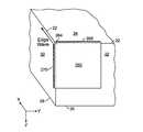
- FIG. 1illustrates the operation of a conventional acoustic touch sensor, an acoustic touchscreen 1 .
- the touchscreen 1has a touch-sensitive area 2 inside of which two-dimensional coordinates of touches are determined.
- the touch-sensitive area 2may include the region bounded by the dashed line 16 which represents the inner boundary of a bezel 10 .
- a first transmitting transducer 3 ais positioned outside of touch-sensitive area 2 and is acoustically coupled to the surface of touchscreen 1 .
- the transducer 3 asends an acoustic signal in the form of an acoustic wave 11 a traveling parallel to the top edge of touchscreen 1 and generally in the plane of touchscreen 1 .
- a first linear array 13 a of partially acoustically reflective elements 4Aligned in the transmission path of acoustic wave 11 a is a first linear array 13 a of partially acoustically reflective elements 4 , each of which partially transmits the acoustic signals and partially reflects them (by an angle of approximately 90°), creating a plurality of acoustic waves (e.g., 5 a , 5 b and 5 c ) traveling vertically across touch-sensitive area 2 .
- the spacing of reflective elements 4is variable to compensate for the attenuation of the acoustic signals with increasing distance from first transmitter 3 a . It is also well known even if reflective elements 4 are uniformly spaced, signal equalization may be achieved by varying the reflective strength of reflective elements 4 .
- Acoustic waves 5 a , 5 b , and 5 care again reflected by an angle of approximately 90° (see arrow 11 b ) by a second linear array 13 b of partially acoustically reflective elements 4 towards a first receiving transducer 6 a upon reaching the lower edge of touchscreen 1 .
- the wavesare detected and converted to electrical signals for data processing. Similar arrangements of reflective elements are located along the left and right edges of touchscreen 1 .
- a second transmitting transducer 3 bgenerates an acoustic wave 12 a along the left edge, and a third linear array 13 c of partially acoustically reflective elements 4 creates a plurality of acoustic waves (e.g., 7 a , 7 b , and 7 c ) traveling horizontally across touch-sensitive area 2 .
- Acoustic waves 7 a , 7 b , and 7 care redirected along 12 b by a fourth linear array 13 d of partially acoustically reflective elements 4 towards receiving transducer 6 b , where they are detected and converted to electrical signals for data processing.
- touch-sensitive area 2is touched at position 8 by an object such as a finger or stylus, a portion of the energy of the acoustic waves 5 b and 7 a is absorbed by the touching object. The resulting attenuation is detected by receiving transducers 6 a and 6 b as a perturbation in the acoustic signal.
- a time delay analysis of the datawith the aid of a microprocessor (not shown) allows determination of the coordinates of touch position 8 .
- the device of FIG. 1can also function as a touchscreen with only two transducers using a transmit/receive transducer scheme.
- a housing 9may be associated with touchscreen 1 .
- the housingcan be made of any suitable material, for example molded polymer or sheet metal.
- the housing 9includes a bezel 10 , indicated by dashed line 16 representing an inner boundary of bezel 10 and dashed line 17 indicating an outer boundary of bezel 10 in FIG. 1 .
- the inner dashed line 16shows that the housing 9 overlays a periphery of touchscreen 1 , concealing the transmitting and receiving transducers, the reflective elements, and other components, but exposing touch-sensitive area 2 . This arrangement can protect the concealed components from contamination and/or damage, provide an aesthetic appearance, and define the touch-sensitive area for the user.
- a touchscreenmay comprise a separate faceplate overlaid on a display panel.
- the faceplateis typically made of glass, but any other suitable substrate may be used.
- the display panelmay be a cathode ray tube (CRT), a liquid crystal display (LCD), plasma, electroluminescent, organic light-emitting-diode (OLED) display, or any other type of display.
- the touch sensitive area 2is surrounded by border regions 15 where the reflective elements 4 and the transmitting and receiving transducers 3 a , 3 b , 6 a and 6 b are located. Reducing the width of border regions 15 increases the touch sensitive area 2 .
- the width of the bordercan be especially important.
- a touch sensor with narrowed border regions 15can be integrated into display monitors that themselves have a narrow border around the displayed image. This feature is desirable as the general market trend for devices such as monitors is towards sleeker and more mechanically compact designs.
- a touch sensor with narrowed border regions 15also is more easily sealed as well as being lighter and can have increased sensor area.
- competing touchscreen technologiese.g., acoustic, capacitive, resistive and infrared
- acoustic touchscreenstend to have wider borders.
- a touch sensorcomprises a substrate.
- the substrateis capable of propagating acoustic waves and includes a first surface having a touch sensitive region.
- a first sidewallintersects the first surface along a first edge.
- the first edgeis configured to propagate a first acoustic wave along the first edge
- the first surfaceis configured to propagate a second acoustic wave across the touch sensitive region.
- a wave converterconverts the first acoustic wave to the second acoustic wave, and the second acoustic wave is based on the first acoustic wave.
- the wave convertermay be a reflective array that coherently scatters and mode converts the first acoustic wave into the second acoustic wave.
- a touch sensor systemcomprises a transmitter for generating a one-dimensional first acoustic wave.
- a touch sensorcomprises a substrate capable of propagating acoustic waves.
- the substrateincludes a first surface having a touch sensitive region.
- First and second sidewallsintersect the first surface along first and second edges.
- the first edgeis configured to propagate the first acoustic wave and the first surface is configured to propagate a second acoustic wave across the touch sensitive region.
- a first converteris provided on the substrate for converting the first acoustic wave to the second acoustic wave.
- a detectoris provided on the substrate for detecting the second acoustic wave after traversing at least a portion of the touch sensitive region. Such detection of the second acoustic wave may be direct or indirect.
- a methodfor detecting a touch on a touch sensitive region of a substrate capable of propagating acoustic waves.
- the substrateincludes a first surface having the touch sensitive region.
- First and second sidewalls of the substrateintersect the first surface along first and second edges.
- the methodcomprises transmitting a one-dimensional first acoustic wave along the first sidewall.
- the first acoustic waveis converted into a second acoustic wave.
- the second acoustic waveis directed along the first surface through the touch sensitive region.
- the second acoustic waveis detected proximate the second sidewall of the substrate.
- Such detection of the second acoustic wavemay be direct or indirect.
- a touch sensorcomprises a substrate capable of propagating acoustic waves.
- the substrateincludes a first surface having a touch sensitive region and a first sidewall intersecting the first surface along a first edge.
- the first edgeis configured to propagate a first acoustic wave along the first edge
- the first surfaceis configured to propagate a second acoustic wave across the touch sensitive region.
- the second acoustic waveis based on the first acoustic wave.
- the touch sensorfurther comprises a reflective array having reflector elements formed on the substrate for mode conversion between the first and second acoustic waves.
- the first edgemay form a curved region.
- the touch sensitive regionhas a surface being one of flat, curved and hemispherical.
- the substratemay further comprise four sidewalls intersecting the first surface along four edges, and form corners with adjacent sidewalls.
- a transduceris mounted at each corner for producing or receiving an acoustic wave, and a reflective array is mounted proximate each of the four edges.
- At least two transducersmay be mounted to the substrate and used to produce or receive acoustic waves.
- the touch sensitive regionreceives touch events having two coordinates which identify a location of a touch event.
- First and second transducersmay be mounted to the substrate to produce and receive acoustic waves for detecting first and second coordinates, respectively, of the touch event on the touch sensitive region.
- At least two transducersmay be mounted to the substrate, wherein at least one of the transducers is used to produce and receive acoustic waves to detect a coordinate of the touch event.
- Transducersare mounted to the substrate for producing and receiving acoustic waves over one of an entire or a portion of the touch sensitive region.
- a second sidewallformed substantially free of defects, intersects the first surface along a second edge. The second edge forms an approximate 90° angle between the second sidewall and the first surface, and the second edge reflects the second acoustic wave after traversing at least a portion of the touch sensitive region.
- one or more reflective stripsare formed proximate the second edge and are spaced apart from each other by an integer times one-half wavelength of the second acoustic wave.
- the reflective strips and the second edgereflect the second acoustic wave after traversing at least a portion of the touch sensitive region.
- a touch sensorcomprises a substrate capable of propagating acoustic waves.
- the substrateincludes a first surface having a touch sensitive region and a first sidewall intersecting the first surface along a first edge.
- the first edgeis configured to propagate a first acoustic wave along the first edge
- the first surfaceis configured to propagate a second acoustic wave across the touch sensitive region.
- the second acoustic waveis based on the first acoustic wave.
- a reflective arraycomprising partially reflective elements is formed on the substrate proximate the first edge for mode conversion between the first and second acoustic waves.
- the partially reflective elementsmay be formed by adding material to the substrate to form protrusions or removing material from the substrate to form grooves.
- a first portion of the partially reflective elementsmay be formed by adding material to the substrate and a second portion may be formed by removing material from the substrate.
- the partially reflective elementsare formed regularly spaced with respect to each other, and may extend along at least one of the first sidewall and the first surface. Additionally, the partially reflective elements may have a length from the first edge of less than a wavelength of the first acoustic wave.
- a first set of regularly spaced partially reflective elementshave a relatively strong Fourier component with respect to a period of one wavelength of the first acoustic wave and simultaneously a minimum Fourier component with respect to a period of one-half wavelength of the first acoustic wave.
- the reflective arraymay be formed of first and second sets of regularly spaced partially reflective elements, wherein the second set is shifted with respect to the first set by one-quarter wavelength of the first acoustic wave, and the first and second sets are superposed on one another.
- the partially reflective elementsmay be formed having a width along the first edge of approximately one-half wavelength of the first acoustic wave.
- a touch sensorcomprises a substrate capable of propagating acoustic waves.
- the substrateincludes a first surface having a touch sensitive region and a first sidewall intersecting the first surface along a first edge.
- the first edgeis configured to propagate a first acoustic wave along the first edge
- the first surfaceis configured to propagate a second acoustic wave across the touch sensitive region.
- the second acoustic waveis based on the first acoustic wave.
- the touch sensorfurther comprises a transducer for generating and receiving acoustic waves which comprises a piezoelectric element, and a reflective array for mode conversion between the first and second acoustic waves.
- the transducermay comprise a diffractive grating positioned along the first edge, a diffractive grating formed on the first sidewall proximate the first edge, or a diffractive grating formed on the first surface proximate the first edge.
- the diffractive gratingmay comprise a series of grooves being spaced apart by approximately one wavelength of the first acoustic wave.
- the diffractive gratingcomprises a series of grooves formed in the substrate which are spaced apart by approximately one wavelength of the first acoustic wave.
- the diffractive gratingcomprises a series of grooves formed in the piezoelectric element.
- the piezoelectric elementmay be one of a pressure-mode piezo and a shear-mode piezo.
- the transducermay further comprise a wedge element bonded to the piezoelectric element.
- the wedge elementis mounted on one of the first sidewall and the first surface, and a grating is positioned on the first edge proximate the wedge element.
- the wedge elementmay be mounted on the first sidewall and form an acute angle with respect to a plane parallel to the first surface, and a grating comprising regularly spaced grooves in the substrate is formed on the first edge proximate the wedge element.
- an angled recessmay be formed by removing material from the substrate, and wedge element, bonded to the piezoelectric element, is mounted within the angled recess.
- the transduceris mounted on a second sidewall which intersects the first surface along a second edge, the second sidewall forming a plane perpendicular to the propagation direction of the first acoustic wave.
- the piezoelectric element of the transducer mounted on the second sidewallmay be a shear-mode piezo.
- the shear-mode piezomay have a poling direction of approximately 45° with respect to the touch surface.
- the piezoelectric elementfurther comprises front and back sides.
- First and second electrodesmay be applied to cover one of a portion and substantially all of the front and back sides of the piezoelectric element, forming an active region corresponding to an area of the piezoelectric element where the first and second electrodes overlap.
- the transduceris bonded to the substrate wherein the bonding corresponds to a portion of the active region and provides strong acoustic coupling to the substrate and the transducer in an area less than one-wavelength squared of the first acoustic wave.
- the first electrodeis applied to cover at least a portion of the front side and a second electrode is applied to cover at least a portion of the front and back sides, wherein first and second electrodes on the front side receive attachments to first and second electrical connections for exciting the piezoelectric element.
- the piezoelectric elementfurther comprises a second edge intersecting each of the front and back sides. The second edge is adjacent to the first edge and occupies a plane perpendicular to the first edge.
- One of the front and back sidesis formed to mount to the substrate and the piezoelectric element is poled in a direction perpendicular to a plane parallel to the front and back sides.
- First and second electrodesare formed on the first and second edges, and the first and second electrodes receive attachments to first and second electrical contacts for exciting the piezoelectric element.
- the piezoelectric elementis mounted to the substrate having a portion of the piezoelectric element extend beyond at least one of the first surface and the sidewall.
- the portion of the piezoelectric element extending beyond at least one of the first surface and the sidewallextends a distance of less than one wavelength of the first acoustic wave.
- FIG. 1illustrates the operation of a conventional acoustic touch sensor, an acoustic touchscreen.
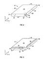
- FIG. 2illustrates a touch sensor substrate having a touch surface and sidewalls in accordance with an embodiment of the present invention.
- FIG. 3illustrates partially reflective arrays formed to perturb edge waves propagating along the edges in accordance with an embodiment of the present invention.
- FIG. 4illustrates an expanded view of a subset of the reflector elements in FIG. 3 in accordance with an embodiment of the present invention.
- FIG. 5illustrates an alternative expanded view of the subset of reflector elements in FIG. 3 in accordance with an embodiment of the present invention.
- FIG. 6illustrates the reflector elements formed on the touch surface in accordance with an embodiment of the present invention.
- FIG. 7illustrates a touch screen having regularly spaced reflector elements in accordance with an embodiment of the present invention.
- FIG. 8illustrates a reflector array design which minimizes back reflection of an edge wave in accordance with an embodiment of the present invention.
- FIG. 9illustrates a grating comprising a series of periodically spaced grooves formed along the edge of the substrate in accordance with an embodiment of the present invention.
- FIG. 10illustrates an expanded view of the grating in accordance with an embodiment of the present invention.
- FIG. 11illustrates a piezoelectric element having wrap-around electrodes that can be used in combination with a diffractive grating to comprise a transducer in accordance with an embodiment of the present invention.
- FIG. 12illustrates an alternating electrical signal being applied to the first and second electrodes of FIG. 11 in accordance with an embodiment of the present invention.
- FIG. 13illustrates the piezo bonded to the sidewalls of the substrate in accordance with an embodiment of the present invention.
- FIG. 14illustrates an edge wave transducer comprising the piezo bonded over the grating in the sidewall of the substrate in accordance with an embodiment of the present invention.
- FIG. 15illustrates an edge wave transducer design incorporating a shear-mode piezoelectric element (shear-mode piezo) in accordance with an embodiment of the present invention.
- FIG. 16illustrates an alternative piezo in accordance with an embodiment of the present invention.
- FIG. 17illustrates a piezo having front and back electrodes on opposite sides of the piezoelectric element in accordance with an embodiment of the present invention.
- FIG. 18illustrates an alternative piezo in accordance with an embodiment of the present invention.
- FIG. 19illustrates a wedge transducer assembly mounted to the sidewall of the substrate in accordance with an embodiment of the present invention.
- FIG. 20illustrates the wedge transducer assembly being tilted with respect to the edge in accordance with an embodiment of the present invention.
- FIG. 21illustrates a wedge transducer assembly mounted to the substrate in accordance with an embodiment of the present invention.
- FIG. 22illustrates an alternative piezo in accordance with an embodiment of the present invention.
- FIG. 23illustrates the piezo mounted to the substrate in accordance with an embodiment of the present invention.
- FIG. 24illustrates an edge wave touch sensor system formed in accordance with an embodiment of the present invention.
- FIG. 25illustrates a touch panel in accordance with in embodiment of the present invention.
- FIG. 26illustrates a touch panel in accordance with an embodiment of the present invention.
- FIG. 27illustrates a large touch panel comprising four piezos in accordance with an embodiment of the present invention.
- FIG. 28illustrates a block diagram of a touch monitor interconnected with a computer in accordance with an embodiment of the present invention.
- FIG. 29illustrates an example of a round table top in accordance with an embodiment of the present invention.
- FIG. 30illustrates an edge-wave packet propagating along an approximate 90° edge of the substrate in accordance with an embodiment of the present invention.
- FIG. 31illustrates an alternative edge wave touch sensor system formed in accordance with an embodiment of the present invention.
- FIG. 32illustrates a touch sensor wherein a single transmit transducer generates X and Y signals in accordance with an embodiment of the present invention.
- FIG. 33illustrates an alternative touch sensor wherein a single transmit transducer generates X and Y signals in accordance with an embodiment of the present invention.
- FIG. 34illustrates a geometry of the substrate near the common transmit transducer in accordance with an embodiment of the present invention.
- FIG. 35illustrates an alternative geometrical option in accordance with an embodiment of the present invention.
- Conventional reflective arrays 13 a - 13 d as shown in FIG. 1range in width between about 5 mm and 15 mm, which corresponds to a range of about 9-26 acoustic wavelengths (assuming a conventional frequency of about 5 MHz, corresponding to a wavelength of about 0.57 mm).
- the reflective arrays having narrower widthsare typically used on smaller screens.
- Acoustic surface wavesconcentrate acoustic energy near a two-dimensional surface.
- the surfacecan be described as guiding the waves, as the acoustic surface waves propagate near the surface without diffusing away from the surface if the surface is flat or even if the surface has a slight curvature.
- One-dimensional edge acoustic wavesare a type of acoustic wave.
- One-dimensional edge acoustic wavesmay be referred to as edge waves, flexural edge waves, or line acoustic waves.
- the wave energy of edge wavesis localized about an edge of a surface and decays approximately exponentially in the directions normal to the edge. Therefore, the energy vector propagates along the edge.
- Edge wavesare non-dispersive; their velocity is independent of frequency. Using non-dispersive waves in touch sensors is advantageous because propagation of acoustic waves will not distort touch-induced perturbations of received signals from their simple dip shape into more complex oscillatory shapes.
- edge waveshaving a frequency of about 5 MHz in glass, this means that an edge wave is confined to within about 1 mm of the edge.
- edge wavesmay propagate along the top edge of a sidewall without being affected by the presence of the bottom edge of the sidewall only 2 mm away.
- edge wave energyis confined to about 1 mm of the edge, it is possible to make a touch sensor with very narrow functional borders using edge wave technology. Therefore, a housing for a touch sensor incorporating edge waves can have a very narrow bezel region, and the touch sensitive area of the touch sensor can be increased.
- FIG. 2illustrates a touch sensor substrate 20 having a touch surface 24 and sidewalls 32 in accordance with an embodiment of the present invention.
- Any suitable materialcan be used for the substrate 20 , including glass, ceramic, and metals (e.g., aluminum or steel).
- metalse.g., aluminum or steel.
- low acoustic loss glassmay be desired.
- borosilicate glasseshave low loss, and can provide increased received signal amplitudes that may in turn enable larger touch sensor areas.
- Clean edges 22are formed on the substrate 20 at an intersection between a plane corresponding to the touch surface 24 and planes corresponding to each of the sidewalls 32 .
- the clean edges 22are formed to be substantially free of defects, such that any deviations on the clean edge 22 such as chips, striations, dents, uneven regions, and the like have dimensions less than the acoustic wavelength.
- the edge-wave wavelengthis only a few percent shorter than the wavelength of the much better known Rayleigh wave. Therefore, making use of the Rayleigh wavelength as a well known and defined measurement, it may be noted that defects are preferably less than 20% of a Rayleigh wavelength.
- the clean edges 22may be formed by any method suitable for the material from which the substrate 20 is manufactured. For example, glass may be cut and machined to provide clean edges 22 . Alternatively, the clean edge 22 may be formed by propagating a controlled fracture using thermal stress, for example by utilizing localized laser heating and gas jet cooling processes. Optionally, the glass may be scribed and broken which, if carefully done, can produce a clean edge 22 opposite the scribed surface.
- Angles 42 and 44 formed where the sidewalls 32 abut the touch surface 24are 90°, or within 20° of 90°, making sidewalls 32 vertical or substantially vertical with respect to the touch surface 24 .
- an edge 22 having an angle 42 or 44 much less than 90°multiple edge wave modes with differing velocities can exist.
- the edge 22has an angle 42 or 44 within +/ ⁇ 10 of 90°, the edge 22 will support only a single edge wave mode. This is desirable as it eliminates the possibility of mode mixing as an edge wave propagates along the edge 22 .
- Opposing edges 26are formed on the substrate 20 at an intersection between a plane corresponding to a second surface 28 of the substrate 20 and the planes corresponding to each of the sidewalls 32 .
- the opposing edges 26do not have to be clean, unless it is desired to also utilize the second surface 28 as a touch surface. If only one touch surface is desired, manufacturing time or cost can be minimized by only having to form clean edges adjacent to one surface.
- FIG. 30illustrates an edge-wave packet 580 propagating along an approximate 90° edge 22 of the substrate 20 in accordance with an embodiment of the present invention.
- the edge wavepropagates in the X direction, as indicated in FIG. 30 .
- the dominant component of material motioni.e. motion of atoms within the substrate 20
- Material deflectionshave been exaggerated in FIG. 30 for clarity. Note that the vast majority of the energy in the edge-wave packet 580 is contained within an edge-wave wavelength distance from the 90° edge 22 along the touch surface 24 and the sidewall 32 .
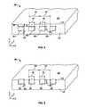
- FIG. 3illustrates partially reflective arrays 30 formed to perturb edge waves propagating along the edges 22 in accordance with an embodiment of the present invention.
- Transducers(not shown) are used to convert between electrical signals and acoustic waves and will be discussed further below.
- electrical signalswill be transmitted between a controller and a transducer to generate and/or receive acoustic signals.
- the reflective arrays 30comprise reflector elements 34 spaced proximate the clean edges 22 to perturb the edge waves propagating along the edges 22 .
- a first wave, the one-dimensional edge waveis generated and propagated along the edges 22 and within one wavelength of the edges 22 .
- the reflective arrays 30can be used to convert the edge waves to second acoustic waves, or two-dimensional surface acoustic waves (SAW), propagating across the touch surface 24 of the substrate 20 .
- SAWsurface acoustic waves
- the reflective arrays 30are reversible, and therefore can also be used to convert the second acoustic wave to a third acoustic wave, or a one-dimensional edge wave.
- the second acoustic wavecan be any type of wave that will provide sufficient touch sensitivity over a two-dimensional touch surface, including surface bound waves like Rayleigh waves (where the term is meant to include quasi-Rayleigh waves) and plate waves (e.g., Lamb and shear waves).
- the reflector elements 34 in FIG. 3are regularly (periodically) spaced apart along edges 22 , and may extend along the sidewalls 32 of the substrate 20 along the Y axis (as shown in FIG. 3 ) and/or extend into the horizontal touch surface 24 . As discussed below, the reflector elements 34 may be formed by either depositing material or removing a portion of the substrate 20 .
- edge waveAs an edge wave travels along the edge 22 and encounters each of the reflector elements 34 , the edge wave is partially transmitted to reach the next reflector element 34 , partially absorbed or scattered by the reflector element 34 , and partially converted by the reflector element 34 to Rayleigh waves bound to the surface 24 through 90° scattering and mode conversion between the one-dimensional edge wave and the two-dimensional Rayleigh surface acoustic wave (SAW).
- SAWRayleigh surface acoustic wave
- FIG. 4illustrates an expanded view of a subset 36 of the reflector elements 34 in FIG. 3 in accordance with an embodiment of the present invention.
- the reflector elements 34are illustrated as protruding reflector elements 86 .
- the reflector elements 86are periodically spaced apart by a distance 48 of approximately a wavelength of the edge waves ( ⁇ E ) traveling along the edge 22 . Therefore, the surface Rayleigh waves launched by the mode conversion by the reflector elements 86 will be synchronous with each other. Many possible shapes are possible for reflector elements 86 .
- the reflector elements 86may be rectangular in shape, having a width 40 along the X axis of approximately ⁇ E /2, a height 38 along the Y axis of approximately ⁇ E or less, and a depth 46 along the Z axis of much less than ⁇ E , such as less than a few percent of ⁇ E .
- the depth 46 dimension of the reflector elements 86extends outward from an outer surface of the sidewall 32 along the Z axis.
- a top edge 80 of the reflector elements 86may be formed flush with the edge 22 or within a distance 82 of the edge 22 .
- the reflector elements 86may be made of any suitable material. For example, fired on ceramics (e.g., glass frit) can be used.
- the reflector elements 86may comprise a loaded-polymer UV-curable ink such as disclosed in U.S. Pat. No. 5,883,457, which is incorporated herein by reference.
- a useful loaded-polymer UV-curable inkis one that is loaded with inorganic particles, and yet is soft compared to the substrate 20 due to its polymer matrix. Reflector elements 86 comprising such loaded polymer inks will induce only minor stiffness perturbations and will couple dominantly via mass loading or inertial effects. Therefore, reflector elements 86 may be fabricated that are mainly mass loading in nature. Reflector elements 86 may be formed on the substrate 20 by any suitable method, such as depositing by screen printing, pad printing, ink jet processes, micro-dispensing, and the like.
- FIG. 5illustrates an alternative expanded view of the subset 36 of reflector elements 34 in FIG. 3 in accordance with an embodiment of the present invention.
- the reflector elements 34are illustrated as grooved reflector elements 88 .
- the reflector elements 88may be formed by removing small regions of the substrate 20 along the sidewalls 32 to form grooves or notches. As illustrated previously, the reflector elements 88 are periodically spaced apart by a distance 48 of approximately a wavelength of the edge wave ( ⁇ E ) traveling along the edge 22 .
- Reflector elements 88can have any of a wide variety of shapes, for example, the reflector elements 88 may be rectangular in shape, having a width 40 along the X axis of approximately ⁇ E /2, a height 38 along the Y axis of approximately ⁇ E or less, and a depth 84 along the Z axis of much less than ⁇ E , such as less than a few percent of ⁇ E .
- the depth 84 dimension of the reflector elements 88extends inward from the outer surface of the sidewall 32 along the Z axis.
- grooved reflector elements 88couple to edge waves more as perturbations in substrate stiffness.
- Reflector elements 88can be back-filled with other materials, such as a soft, loaded polymer, for example, to tune the mass-loading and stiffness-perturbation characteristics of the reflector elements 88 .
- FIG. 6illustrates the reflector elements 34 formed on the touch surface 24 in accordance with an embodiment of the present invention.
- the reflector elements 34are periodically spaced apart by the distance 48 of approximately a wavelength of the edge waves ( ⁇ E ) traveling along the edge 22 .
- the reflector elements 34have the width 40 along the X axis of approximately ⁇ E /2, the height 38 along the Z axis of approximately ⁇ E or less, and a depth (not shown) along the Y axis.
- the depth dimensionmay extend outward from an outer surface of the touch surface 24 if the reflector elements 34 are formed of additional material, or extend inward from the outer surface of the touch surface 24 if the reflector elements 34 are formed by removing material from the substrate 20 .
- reflector elements 34may be formed on both the touch surface 24 and sidewalls 32 such as by combining the reflector elements 34 of FIG. 3 with the reflector elements 34 of FIG. 6 .
- edge wave power densityis very close to zero when more than a wavelength away from the edge 22 , structures more than one wavelength away will have essentially no coupling to the edge wave.
- any perturbation of the edge 22 and any perturbation within one wavelength of the edge 22 on the touch surface 24 or the sidewalls 32will scatter edge wave energy. Therefore, by varying the nature (mass loading, stiffness perturbation, etc.), geometry and location of the reflector elements 34 , the relative strengths of coupling between the edge wave and various other acoustic modes (Rayleigh waves, Lamb waves, shear waves, etc.) can be tuned.
- edge waves and Rayleigh wavesCoupling between edge waves and Rayleigh waves is of interest.
- High touch sensitivity and lack of dispersionmake Rayleigh waves attractive as a touch sensing acoustic mode.
- the depth profiles of Rayleigh waves and edge wavesare very similar thus making strong and preferential coupling to Rayleigh waves easier than edge wave coupling to other modes.
- Numerical simulationsmay be used to optimize the perturbation design to optimize edge wave coupling to Rayleigh waves or to an alternate touch-sensitive acoustic mode.
- each individual reflector element 34is intended to reflect only a small portion of the incident edge wave energy, and therefore in the case of the grooved reflector elements 88 of FIG. 5 , the depth 84 into the substrate 20 is generally much less than ⁇ E , e.g., of order of a percent of a wavelength or a few microns, and can be adjusted to achieve desired tradeoffs between acoustic loss and conversion efficiency between the one-dimensional edge waves and the two-dimensional surface acoustic waves.
- the reflective arrays 30can be designed to couple edge waves to Rayleigh waves that propagate across the touch surface 24 at a diagonal angle, rather than perpendicular to the edge 22 .
- FIG. 7illustrates a touch screen 128 having regularly spaced reflector elements 34 in accordance with an embodiment of the present invention.
- reflector elements 34are illustrated on only two of the four edges 22 , namely for the transmitting reflector element array 176 and receiving reflector element array 178 . It should be understood that the reflector elements 34 may be formed as discussed previously in FIGS. 3-6 .
- the reflector elements 34are periodically spaced apart by the distance 48 of approximately a wavelength of the edge wave ( ⁇ E ) traveling along the edge 22 .
- Arrows 164 , 174 , and 166illustrate a desired acoustic path from transmit transducer 162 to the receive transducer 168 . Also illustrated in FIG. 7 are undesired acoustic paths leading to interfering signals at receive transducer 168 . The undesired acoustic paths are caused by 180° backscattering of edge waves by the reflector arrays 176 and 178 .
- the array of regularly spaced reflector elements 34 having wavelength spacing (distance 48 ) as needed for 90° scattering of SAW to edge wavesmay also lead to 180° backscattering of the edge wave.
- a first edge waveis propagated by the transmit transducer 162 along edge 22 in the direction of arrow 164 .
- the edge waveis converted by the reflector elements 34 of the transmitting reflector element array 176 to a SAW wave traveling across the touch surface 24 in the direction of arrow 174 .
- Some of the edge wave power from transmit transducer 162will continue propagating along the edge 22 as shown by arrow 184 . If reflector elements 34 backscatter edge waves by 180°, an undesired edge wave will be generated in the direction of arrow 185 . This undesired edge wave will also be scattered and mode converted at 90°, thus contributing an undesired delayed contribution to the Rayleigh wave (arrow 174 ), eventually leading to a parasitic interfering signal at receive transducer 168 .
- 180° edge-wave backscatteringalso generates undesired parasites at the receiving reflector element array 178 .
- the desired SAW wave(arrow 174 ) is converted to two edge waves by the regularly spaced reflector elements 34 of the receiving reflector element array 178 . Therefore, a second edge wave traveling in the direction of arrow 166 to receiving transducer 168 and an undesired parasitic edge wave traveling in the direction of arrow 186 are created.
- the parasitic edge wavemay then be backscattered by 180° back towards the receive transducer 168 by the reflector elements 34 as illustrated by arrow 187 . It is desirable to design reflector elements 34 in such a manner to minimize the 180° edge-wave backscattering in order to minimize the amplitudes of the parasitic paths shown in FIG. 7 .
- FIG. 8illustrates a reflector array design 150 which minimizes back reflection of an edge wave in accordance with an embodiment of the present invention. Such designs are applicable to both transmit and receive arrays such as items 176 and 178 of FIG. 7 .
- First and second reflector elements 152 and 154are illustrated on the touch surface 24 of the substrate 20 , but it should be understood that the first and second reflector elements 152 and 154 may be formed on the sidewalls 32 in addition to, or instead of, the touch surface 24 .
- the first and second reflector elements 152 and 154may be formed as grooves or protrusions.
- the first reflector elements 152are spaced 1 wavelength of the edge wave apart with respect to each other.
- the second reflector elements 154are shifted with respect to the first reflector elements 152 by a distance 182 substantially equivalent to one-quarter wavelength of the edge wave.
- First and second reflector elements 152 and 154have a width 180 of less than one-quarter wavelength, equal to one-quarter wavelength, or larger than one-quarter wavelength, in which case reflector elements 152 and 154 are overlapping or superposed.
- the reflector array design 150may be created by first designing the first reflector elements 152 without regard to the need to suppress 180° back reflection of edge waves.
- the first reflector elements 152are then shifted by one-quarter wavelength (in either direction) to create the second reflector elements 154 .
- the second reflector elements 154are then superposed on the first reflector elements 152 .
- a SAW wave 158 and a reflected wave 170are created by the first reflector 152 .
- a SAW wave 160 and a reflected wave 172are created by the second reflector 154 . Therefore, two SAW waves are created at 90° and 2 reflected edge waves are created at 180° with respect to the direction of propagation of the edge wave.
- the reflected waves 170 and 172have an extra one-half wavelength path and hence a relative phase shift of 180° which substantially cancels or minimizes the 180° back reflection.
- 180° backscatteringwill be suppressed while 90° edge-SAW coupling will not be suppressed.
- the reflector elements 86 and 88are one-half wavelength wide and spaced 1 wavelength apart. This corresponds to a case of FIG. 8 wherein the first and second reflector elements 152 and 154 are each one-quarter wavelength wide and spaced 1 wavelength apart.
- the first reflector elements 152are replicated, shifted by one-quarter wavelength and superposed, the result is a series of reflector elements 86 or 88 having a width 40 of one-half wavelength and being positioned apart the distance 48 of one wavelength.
- a transducermay be used to convert electrical signals to acoustic edge waves that propagate along the edge 22 .
- a transducer assemblyis a piezoelectric element in combination with a grating element, where the grating element is disposed between the piezoelectric element and the medium, such as substrate 20 , in which the generated acoustic mode is to propagate.
- the gratingacts as a diffractive element that couples acoustic energy from the transducer to acoustic waves on the substrate 20 .
- FIG. 9illustrates a grating 50 comprising a series of periodically spaced grooves 52 formed along the edge 22 of the substrate 20 in accordance with an embodiment of the present invention.
- the grooves 52can be formed in the substrate 20 using any suitable manufacturing method, for example, machining, etching, laser ablation, grinding, patterning, molding, and the like.
- FIG. 10illustrates an expanded view of the grating 50 in accordance with an embodiment of the present invention.
- a height 54 along the Y axis of the grooves 52is approximately equal to or less than a wavelength of the edge wave ⁇ E .
- a depth 58 of the grooves 52 along the Z axisis approximately equal to or much less than the wavelength of the edge wave ⁇ E .
- the grooves 52are spaced apart by a distance 74 which is approximately equal to the wavelength of the edge wave ⁇ E .
- the width 56 of the grooves 52 along the X axisis approximately one-half the wavelength of the edge wave, or ⁇ E /2.
- the design of the grating 50has much in common with the design of reflector arrays comprising grooved reflector elements 88 as shown in FIG.
- the grating 50must excite or extract much of the energy of an edge wave in the short length of grating 50 while reflector arrays 30 in FIG. 3 spread out the coupling between edge waves and Rayleigh waves across most of the lengths of the edges 22 .
- the depth 58 in grating 50is typically significantly deeper than depth 84 in FIG. 5 .
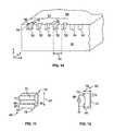
- FIG. 11illustrates a piezoelectric element 90 having wrap-around electrodes that can be used in combination with a diffractive grating to comprise a transducer in accordance with an embodiment of the present invention.
- a first electrode 64is present on a lower region 65 of a front side 66 of the piezoelectric element 90 and wraps around a bottom side 76 of the piezoelectric element 90 to a back side 70 of the piezoelectric element 90 .
- a second electrode 72is present on an upper region 73 of the front side 66 of the piezoelectric element 90 .
- the first and second electrodes 64 and 72may be comprised of silver frit, printed nickel, or any other conductive material.
- the assembly comprising the piezoelectric element 90 and electrodes 64 and 72is often referred to as a piezo 60 .
- the piezoelectric element 90is a pressure mode piezoelectric element.
- PZTa lead-zirconium-titanate ceramic
- PVDFpolyvinylidene fluoride
- lead-free ceramicsmay also be used.
- the height of the active region of the piezo 60is matched to the vertical profile of the edge wave, i.e., approximately equal to ⁇ E or less.
- the active region of the piezo 60is determined by the geometry of the electrode 72 as only the piezoelectric material sandwiched between electrodes 72 and 64 is mechanically excited when a voltage is applied to the electrodes 72 and 64 .
- the piezo dimension 62can extend beyond the active region and hence is allowed to be much larger than the edge wave wavelength ⁇ E .
- FIG. 12illustrates an alternating electrical signal 96 being applied to the first and second electrodes 64 and 72 of FIG. 11 in accordance with an embodiment of the present invention.
- the geometry of the wrap-around first electrode 64 and the second electrode 72causes only the upper region 73 of the piezo 60 to be electrically active.
- Piezoelectric elements 90typically have a thickness 78 corresponding to one-half wavelength of acoustic waves in the piezoelectric material at the operating frequency. (For clarity, the thickness of electrodes 64 and 72 are exaggerated in FIG. 12 .) For a pressure-mode piezo 60 operated at about 5 MHz, the thickness 78 is typically about 400 ⁇ m. Electrical connection to the first and second electrodes 64 and 72 can be made using any suitable method, for example, by spring contacts, solder, conductive epoxy (e.g., silver loaded), or a conductive adhesive with directional conductivity (e.g., a Z-axis adhesive having significant conductivity only perpendicular to the plane of the electrodes 64 and 72 ). Attributes to consider when determining connection methods include a low resistance junction, low electromagnetic interference and susceptibility, high reliability, low cost and the like.
- FIG. 13illustrates the piezo 60 bonded to the sidewalls 32 of the substrate 20 in accordance with an embodiment of the present invention.
- Four piezos 60are bonded in four different locations along the four different edges 22 .
- FIG. 14illustrates an edge wave transducer 98 comprising the piezo 60 bonded over the grating 50 in the sidewall 32 of the substrate 20 in accordance with an embodiment of the present invention.
- the piezos 60are bonded over the grooves 52 in the grating 50 , with the electrically active upper region 73 overlapping the grooves 52 .
- An adhesivecan be used to bond the piezo 60 over the grating 50 such that the adhesive fills or partially fills the grooves 52 .
- the mechanical properties of the adhesivecan be chosen so that the motions of the piezo 60 are largely decoupled from the sidewall 32 of the substrate 20 in the region of the grooves 52 .
- the grating 50may be designed to provide strong acoustic coupling between the piezo 60 and the grooves 52 .
- a grating(not shown) can be formed on a side of the piezo 60 instead of on the sidewall 32 of the substrate 20 so that no grating 50 need be fabricated in substrate 20 .
- the grating side of the piezo 60can then be bonded to the substrate 20 to provide the coupling mechanism between acoustic waves generated by the piezo 60 and an edge wave.
- edge wave transducer 98may instead be mounted to the touch surface 24 of the substrate 20 .
- edge wave transducer 98may be formed on both the sidewalls 32 and touch surface 24 .
- FIG. 15illustrates an edge wave transducer design 100 incorporating a shear-mode piezoelectric element (shear-mode piezo) 120 in accordance with an embodiment of the present invention.
- the shear-mode piezo 120comprises a piezoelectric material 118 having front side 138 , back side 184 , and first, second, third and fourth sides 188 - 194 .
- a first electrode 122is present on a triangular shaped region 136 on the front side 138 of the piezoelectric material 118 .
- the second electrode 124is present on a bottom triangular region 196 on the front side 138 of the piezoelectric material 118 and wraps around the bottom side 148 to the back side 184 of the piezoelectric material 118 .
- the shear-mode piezo 120is bonded to the sidewall 32 of the substrate 20 and abuts the touch surface 24 .
- the shear-mode piezo 120is electrically active in the upper left hand corner corresponding to the region 136 and generates motion with polarization or a component of polarization at approximately a 45° angle with respect to the X and Y axes as indicated by double arrow 127 .
- the shear motion of the shear-mode piezo 120then couples to an edge wave propagating in the Z direction as indicated by arrow 126 . Note that the shear-mode piezo 120 directly excites the edge wave; there is no need for a grating structure such as item 50 .
- FIG. 16illustrates an alternative piezo 200 in accordance with an embodiment of the present invention.
- a front electrode 204is present on a upper region 206 of a front side 208 of a piezoelectric element 202 .
- a back electrode 210is present on a lower region 212 on the front side 208 of the piezoelectric element 202 and wraps around a bottom side 214 to a back side 216 of the piezoelectric element 202 .
- the back electrode 210extends along the back side 216 to cover the upper region 206 of the piezoelectric element 202 only in an active region 218 .
- a first electrical connection 220is interconnected with the front electrode 204 by soldering, wire-bonding, or other interconnection methods.
- a second electrical connection 222is interconnected with the back electrode 210 .
- the size of the piezo 200is larger than the active region 218 to allow room to connect the first and second electrical connections 220 and 222 to the front and back electrodes 204 and 210 for ease of manufacturing, while limiting the size and shape of the active area 218 to prevent scattering too much energy.
- Opposite polaritiesare applied to the front and back electrodes 204 and 210 .
- the size of the active area 218is, by way of example only, of order of one-tenth of a square edge-wave wavelength, i.e. ⁇ 0.1* ⁇ E 2 .
- FIG. 16illustrates an example where the active area 218 is square in shape. Other shapes for the active area 218 are possible with appropriate shaping of electrodes 204 and 210 to produce the desired overlap geometry.
- the piezos in FIGS. 15 and 16limit excitation of the substrate 20 to a small region corresponding to the cross sectional area of a propagating edge wave.
- piezoelectric excitationis limited to the desired edge-wave cross-sectional area.
- An alternate approachis to piezoelectrically excite a larger piezo area, such as create a larger active area 218 , but limit mechanical coupling between the piezo 200 and the substrate 20 to the small cross-sectional area of the propagating edge wave.
- FIG. 17illustrates a piezo 224 having front and back electrodes 226 and 228 on opposite sides of piezoelectric element 246 in accordance with an embodiment of the present invention.
- a front electrode 226 and a back electrode 228substantially cover a front side 254 and back side 256 , respectively, of a piezoelectric element 246 .
- the piezo 224is poled to produce a shear-mode piezo with shear motion in a 45° direction.
- a stiff adhesivesuch as epoxy may be used in the desired active area to accomplish strong mechanical coupling to the substrate 20 while an air gap or a weak shear coupling material such as silicone rubber (RTV) can be used elsewhere.
- RTVsilicone rubber
- a wrap around electrodemay be used as shown in FIG. 18 .
- FIG. 18illustrates an alternative piezo 230 similar to that shown in FIG. 17 in accordance with an embodiment of the present invention.
- a front electrode 232is present on a front side 234 of a piezoelectric element 236 .
- a back electrode 238is present on a corner region 240 on the front side 234 of the piezoelectric element 236 and wraps around a portion of a side 242 to a back side 244 of the piezoelectric element 236 .
- the back electrode 238extends along the back side 244 to cover the piezoelectric element 236 , forming an active region where the front electrode 232 and back electrode 238 overlap.
- nearly the entire area of the piezo 230is piezoelectrically active.
- Appropriate design and fabrication of the bond between the piezo 230 and the substrate 20limit the acoustic coupling to the substrate 20 to the desired region for edge-wave generation and reception.
- FIG. 19illustrates a wedge transducer assembly 130 mounted to the sidewall 32 of the substrate 20 in accordance with an embodiment of the present invention.
- a piezoelectric element 250is mounted to one side of a wedge 252 .
- An opposing side of the wedge 252is mounted to the sidewall 32 of the substrate 20 .
- the tilt of piezo element 250 with respect to the vertical surface of sidewall 32defines an angle 248 of the wedge 252 .
- This wedge angle 248is controlled so that bulk pressure waves excited by the piezo 250 and propagating in the wedge 252 can couple to vertically propagating Rayleigh waves on sidewall 32 of substrate 20 .
- the piezoelectric element 250launches a bulk wave in the wedge 252 .
- a surface acoustic Rayleigh wave (SAW)is launched and propagates along the sidewall 32 as indicated by arrow 132 ; therefore propagating perpendicular to edge 22 in FIG. 19 .
- the Rayleigh wavein turn interacts with the grating 50 which comprises grating elements 52 .
- the grating elements 52have a height 54 in the Y axis direction approximately equal to or less than the wavelength of an edge wave ⁇ E and are spaced apart by approximately ⁇ E .
- the width 56 of the grating elements 52is approximately ⁇ E /2.
- the grating 50can couple two-dimensional surface waves (the Rayleigh waves) to a one-dimensional edge wave, thereby launching an edge wave as indicated by arrow 134 along the edge 22 .
- the transducer design of FIG. 19may lead to a parasitic SAW path between transmit/receive pairs of wedge transducer assemblies 130 .
- parasitic components of the first SAW launched by the wedge transducer assembly 130can propagate up the sidewall 32 , across the sensor surface 24 , and down the opposite sidewall 32 to a receiving wedge transducer placed on the opposite sidewall 32 .
- This parasitic pathcan be interrupted by tilting the wedge transducer assembly 130 with respect to the edge 22 .
- FIG. 20illustrates the wedge transducer assembly 130 being tilted with respect to the edge 22 in accordance with an embodiment of the present invention. Therefore, the angle of intersection between the Rayleigh wave launched by the wedge transducer assembly 130 and the edge 22 is different than 90°.
- FIG. 21illustrates a wedge transducer assembly 130 mounted to the substrate 20 in accordance with an embodiment of the present invention.
- a portion of the substrate 20 of the opposing surface 28 opposite the touch surface 24can be removed to form an angled recess 140 at a corner proximate intersecting planes formed by two of the sidewalls 32 .
- the wedge transducer assembly 130 including the wedge 142 and the piezoelectric element 144can be mounted in the recess 140 . Therefore, wedge transducer assembly 130 does not protrude beyond the planes of the sidewalls 32 or substrate surfaces 24 and 26 .
- FIG. 22illustrates an alternative piezo 260 in accordance with an embodiment of the present invention.
- the piezo 260comprises a piezoelectric element 262 having a notched corner 264 .
- the notched corner 264may be formed having an angle 266 of approximately 45° with respect to planes formed by first and second edges 268 and 270 of the piezoelectric element 262 .
- the piezoelectric element 262may be approximately 200 microns in depth 272 along the Z axis. More generally, depth 272 is chosen so that there is a shear-mode resonance at the operating frequency, that is, depth 272 is approximately equal to one-half of a bulk shear wave wavelength in the material of piezoelectric element 262 .
- the width 274 and height 276 along the X axis and Y axis, respectively, of the piezoelectric element 262may each be 2 mm.
- First and second electrodes 278 and 280may be formed on the first and second sides 268 and 270 , respectively. Poling is accomplished along the Z axis.
- FIG. 23illustrates the piezo 260 mounted to the substrate 20 in accordance with an embodiment of the present invention. Mounting is similar to that shown in FIG. 15 for the shear-mode piezo 120 .
- the piezo 260may be mounted to the substrate 20 having the notched corner 264 mounted flush with edge 22 as shown in FIG. 23 .
- piezo sides 268 and 270may be flush with surfaces of substrate 20 .
- the piezo 260By mounting the piezo 260 such that the piezo sides 268 and 270 form an overhang beyond the touch surface 24 and sidewall 32 , greater efficiency may be achieved.
- the amount of overhang, or the distance the piezo sides 268 and 270 extend beyond the touch surface 24 and sidewall 32may be equal to or less than an edge-wave wavelength.
- the overhang designmay be applied equally to transducers based on the piezo design of FIGS. 15 , 16 and 18 , as well as the transducer design of FIG. 14 .
- wires 282 and 284may be attached to the first and second electrodes 278 and 280 as previously discussed.
- motion, or shear-mode oscillationis generated within the piezoelectric element 262 as indicated by arrows 288 - 294 .
- the strength of the vibrationis stronger within the piezoelectric element 262 close to the notched corner 264 , as indicated by arrow 288 . Moving further away from the notched corner 264 , the strength of the vibration and amplitude of the shear-wave decreases in a controlled manner.
- the basic edge-wave excitation mechanismis the same for the shear-mode piezo 120 and piezo 260 in FIGS. 15 and 23 , respectively.
- An advantage of piezo 260 of FIGS. 22 and 23is that by appropriate design of the notch 264 geometry and the placement of the piezo 260 on substrate 20 , the piezoelectric excitation pattern can be closely matched to the cross sectional profile of edge wave motion. This maximizes the ratio of piezo coupling to the desired edge-wave mode relative to parasitic coupling to other modes.
- piezossuch as piezo 260
- piezo 260are very small and have high impedance when compared to the impedances of 50 ⁇ of conventional transducers used to generate the SAW.
- impedanceis inverse with respect to the size of the active area, impedance is now into the k ⁇ region. Therefore, it should be understood that the controllers, such as the controller 112 in FIG. 24 , are preferable designed to match the high impedance of the piezos.
- Known electronic principlesmay be used, such as matching the input impedance of the receiver circuit to the impedance of the receive transducer.
- FIG. 24illustrates an edge wave touch sensor system 300 formed in accordance with an embodiment of the present invention.
- the touch sensor system 300comprises the substrate 20 having the touch surface 24 and sidewalls 32 (not shown).
- the edges 22have been indicated as edges 306 , 308 , 310 and 312 .
- a controller 112supplies electrical signals to transmitting transducers 302 and 304 via electrical connections 110 to excite the piezos of the transmitting transducers 302 and 304 .
- Gratings 92 and 94convert piezo vibrations to a first acoustic mode, such as edge wave 314 traveling along edge 306 and edge wave 316 traveling along edge 308 , respectively, as indicated by arrows.
- the edge wave 314is converted by reflective array 318 into Rayleigh wave 320 .
- the Rayleigh wave 320travels as a surface acoustic wave bound to the surface 24 until it encounters reflective array 322 , where it is converted back into an edge wave 324 and travels along the edge 310 in the direction indicated by an arrow where it can be detected by receiving transducer 326 .
- the edge wave 316is converted by reflective array 328 into Rayleigh wave 330 .
- the Rayleigh wave 330travels as a surface acoustic wave bound to the surface 24 until it encounters reflective array 332 , where it is converted back into an edge wave 334 and travels along the edge 312 in the direction indicated by an arrow where signal amplitudes of the edge wave can be detected by receiving transducer 336 .
- Electrical connections 114are made so that receiving transducers 326 and 336 can supply electrical signals back to the controller 112 .
- Perturbationse.g., a touch with a finger or stylus
- the electrical connections 110 and 114can comprise cable harnesses.
- a touch sensitive region 108is formed on the touch surface 24 and comprises essentially the entire touch surface 24 because the reflective arrays 318 , 322 , 328 , and 332 and transducers 302 , 304 , 326 , and 336 may be formed along and/or joined to a very narrow outer periphery 116 of the sensor substrate 20 , and in many cases can be made on and/or joined to the sidewalls 32 of the substrate 20 .
- the outer periphery 116 of the touch surface 24 that is needed for the generation and detection of the one-dimensional edge wavescan be as little as 1 mm.
- the surface acoustic wave(e.g., two-dimensional SAW) can be detected directly after traversing at least a portion of the touch sensitive region 108 without being converted to an edge wave to identify the presence and location of perturbations to the touch sensitive region 108 of the touch surface 24 .
- FIG. 24may be modified to provide two-dimensional touch position coordinates using two transmit/receive transducers as discussed previously.
- many other touchscreen geometries using edge wavesare possible, including touchscreen designs with non-orthogonal acoustic paths that can be adapted for use with edge waves.
- FIG. 25illustrates a touch panel 350 in accordance with in embodiment of the present invention.
- Clean edges 356 - 362are formed on the substrate 20 .
- Reflector elements 364 and 366are formed on the sidewall 32 or touch surface 24 proximate two of the edges 356 and 362 .
- the reflector elements 364are illustrated as being formed on the sidewall 32 proximate the edge 356 and the reflector elements 366 are illustrated as being formed on the touch surface 24 proximate the edge 362 .
- Piezos 352 and 354are used to both transmit and receive edge wave information.
- a controller 368may communicate with each of the piezos 352 and 354 via electrical connections 370 and 372 .
- the controller 368may have switches 374 and 376 to control which piezo 352 or 354 is connected to a signal generator 378 for transmitting a signal or an electronics module 380 for receiving and decoding a signal.
- the controller 368may alternate between the piezos 352 and 354 , wherein the piezo 352 may transmit and receive a signal followed by the piezo 354 transmitting and receiving a signal.
- electrical connections 370 and 372may each be provided with one of two identical circuits each with a transmit/receive mode switch.
- the piezo 352Upon activation, the piezo 352 transmits an edge wave in the direction of arrow 382 .
- the edge waveencounters the reflector elements 364 and is converted to a SAW coupled to the surface of the touch surface 24 and transmitted in the direction of arrow 384 .
- a significant fraction of SAW propagating in direction 384will be reflected by edge 360 .
- one or more reflective strips 386may be placed one-half wavelength apart on the touch surface 24 proximate and parallel to the edge 360 .
- the edge 360 and/or the reflective strips 386reflect the SAW by 180° in the direction of arrow 388 .
- the SAWencounters the edge 356 and the reflector elements 364 , the SAW is converted to an edge wave transmitted in the direction of arrow 390 .
- the edge waveis detected by the piezo 352 and the electrical signal is read by the controller 368 via the electrical connection 370 .
- the controller 368then transmits an electrical signal from the signal generator 378 over the electrical connection 372 to excite piezo 354 .
- the piezo 354generates an edge wave traveling along the edge 362 in the direction of arrow 392 .
- the edge waveencounters the reflective elements 366 , the edge wave is converted to a SAW traveling across the touch surface 24 in the direction of arrow 394 .
- the SAWis reflected 180° by the edge 358 and/or one or more reflective strips 396 .
- the reflected SAWtravels in the direction of arrow 398 , encounters the edge 362 and reflective elements 366 , and is converted to an edge wave traveling in the direction of arrow 400 .
- the piezo 354detects the edge wave and sends an electrical signal over the electrical connection 372 to the controller 368 .
- FIG. 31illustrates an alternative edge wave touch sensor system formed in accordance with an embodiment of the present invention.
- a single transducer 602operates in both transmit and receive modes to provide two-dimensional touch coordinate information while utilizing a very narrow border region of the touch surface 24 .
- the transducer 602may be any transducer design capable of transmitting and receiving edge waves, such as transducer designs previously discussed.
- the substrate 20is formed having clean edges 604 - 610 .
- a rounded corner 612is formed where the edges 604 and 606 intersect.
- the rounded corner 612is also formed having a substantially clean edge, and may have an angle of approximately 90°.
- Reflector arrays 614 and 616are formed on the edges 604 and 606 , respectively.
- An absorbing damper 618is formed on one end of the sidewall 32 proximate the edge 608 and proximate one end of the reflective array 616 .
- the waveguide properties of the edgeenable a very simple and efficient way to redirect edge waves by 90° between the reflector arrays 614 and 616 for acquiring both X and Y touch data, namely, the sidewall 32 may be formed having a simple quarter-circle shaping of the sidewall 32 and corresponding edges 604 and 606 .
- the transducer 602transmits an edge wave in the direction of arrow 620 along the edge 604 .
- a portion of the transmitted edge waveis scattered by the reflector array 614 and traverses the touch surface 24 in the direction of arrow 622 as a Rayleigh wave.
- the waveis reflected by 180° in the direction of arrow 624 and again by the reflector array 614 in the direction of arrow 626 to be received by the transducer 602 .
- This portion of the transmitted edge waveis received relatively early in time and provides a measurement of the X coordinate of a touch.
- Another portion of the transmitted edge-wave from the transduceris transmitted through the reflector array 614 , follows the rounded corner 612 and encounters the reflector array 616 .
- the edge-wave poweris partially scattered at 90° as a Rayleigh wave in the direction of arrow 628 and traverses the touch surface 24 as a Rayleigh wave.
- the waveis reflected by 180° by the edge 610 in the direction of arrow 630 , and reflected by the reflector array 616 and received by the transducer 602 .
- This portion of the transmitted edge-waveis received relatively late in time and provides a measurement of the Y coordinate of a touch. Any remaining portion of the transmitted edge-wave that is transmitted through both the reflector arrays 614 and 616 may be eliminated with the absorbing damper 618 .
- FIG. 26illustrates a touch panel 402 in accordance with an embodiment of the present invention.
- the touch panel 402comprises a substrate 20 with sidewalls 32 as discussed previously. Clean edges 404 - 410 have been formed at an intersection between the planes of each of the sidewalls 32 and the touch surface 24 .
- the substrate 20is formed having one dimension of the touch surface 24 greater than the other. For example, the substrate 20 along the X dimension is longer than in the Y direction.
- Reflector elements 420 , 422 and 424have been formed proximate the edges 406 , 410 and 404 , respectively. As discussed previously, the reflector elements 420 - 424 may be formed as regularly spaced grooves or protrusions on the sidewalls 32 and/or the touch surface 24 . Optionally, one or more reflective strips 426 may be formed on the touch surface 24 proximate the edge 408 .
- the touch panel 402uses three piezos 412 , 414 and 416 .
- the piezo 412may be used to transmit signals while the piezo 414 is used to receive signals.
- a signal generator 428 within controller 418transmits a signal over electrical connection 430 .
- the transmitting piezo 412launches an edge wave along edge 406 in the direction of arrow 432 .
- the edge waveis partially reflected by the reflector elements 420 and is converted to a SAW moving across the touch surface 24 in the direction of arrow 434 .
- the SAWis converted to an edge wave by the reflector elements 422 and travels along the edge 410 in the direction of arrow 436 .
- the piezo 414detects the edge wave and sends an electrical signal to the controller 418 via electrical connection 438 .
- the piezo 416is used for both transmitting and receiving signals. This may be accomplished as discussed previously in connection with FIG. 25 and the controller 368 .
- the piezo 416is excited by an electrical signal from the signal generator 428 of the controller 418 via electrical connection 440 .
- the piezo 416launches an edge wave along edge 404 in the direction of arrow 442 , which is partially reflected by the reflector elements 424 in the direction of arrow 444 as a SAW.
- the SAWis reflected 180° by the reflective strip 426 and/or the edge 408 in the direction of arrow 446 .
- the SAWis reflected by the reflector elements 424 and converted to an edge wave propagating in the direction of arrow 448 .
- the edge waveis detected by the piezo 416 and an electrical signal is sent to the controller 418 over the electrical connection 440 .
- the touch panel 402utilizes one piezo 416 with reflector elements 424 and the edge 408 (and optionally the reflector strip 426 ) to detect touch events along the X axis.
- the two piezos 412 and 414 and the reflector elements 2420 and 422are used. Therefore, the SAW traverses the touch surface 24 along the X axis only once, while the SAW traverses the touch surface 24 along the Y axis twice.
- FIG. 27illustrates a large touch panel 450 comprising four piezos 452 - 458 in accordance with an embodiment of the present invention.
- the touch panel 450may comprise a large touch surface 24 on the substrate 20 . Therefore, the distance the waves have to travel becomes increasing longer and the signal experiences increased attenuation.
- the design in FIG. 27minimizes the maximum path length while having a single transducer at each corner. Note that at most one transducer of the designs in FIGS. 15-18 and 23 can be placed at each corner of the substrate 20 .
- the piezos 452 - 458are mounted at different corners of the substrate 20 and thus do not physically interfere with each other. Each of the piezos 452 - 458 both transmit and receive signals as discussed previously in FIG. 25 , and therefore the controller 418 will not be further discussed.
- the substrate 20is formed having clean edges 460 - 466 .
- Reflector elements 470 - 476are formed proximate each of the edges 460 - 466 along a length of approximately one-half of each of the edges 460 - 466 closest to the piezos 452 - 458 .
- Reflective strips 494 - 498may be formed on the touch surface 20 parallel to the edge 466 and spaced apart by a distance of approximately one-half surface acoustic wavelength.
- the reflective strips 494 - 498are formed along approximately one-half of the length of the edge 466 where the reflector elements 476 are not present, or the half of the edge 466 furthest away from the piezo 456 . Additional reflective strips are formed on the touch surface 20 parallel to each of the edges 460 - 464 in the same manner.
- the piezo 452When the piezo 452 is excited, the piezo 452 launches an edge wave along the edge 462 in the direction of arrow 478 .
- the edge waveis partially reflected by the reflector elements 472 and converted to a SAW traveling across the touch surface 24 in the direction of arrow 480 .
- the SAWis reflected by 180° in the direction of arrow 482 by the reflective strips 494 - 498 and/or the edge 466 .
- the SAWis reflected 90° by the reflector elements 472 in the direction of arrow 484 and received by the piezo 452 . Therefore, the piezo 452 detects a signal representative of a Y coordinate of one-half of the touch surface 24 , such as area 486 .
- the piezos 454 , 456 and 458each send and receive signals in the manner described for piezo 452 , detecting a signal over an area of approximately one-half of the touch surface 24 .
- the piezo 454detects a signal representative of an X coordinate of an area 488 .
- the piezo 456detects a signal representative of a Y coordinate of an area 490 .
- the piezo 458detects a signal representative of an X coordinate of an area 492 . Therefore, compared to touch panels that use two piezos to transmit and receive signals, the touch panel 450 uses four piezos 452 - 458 which receive signals from a signal path reduced in length compared to the two piezo geometry.
- the edge wavesdo not have to travel as far and larger touch panels 450 may be implemented. Also, there is no physical interference between piezos 452 - 458 as each of the piezos 452 - 458 is mounted on a different corner of the substrate 20 .
- FIG. 32illustrates a touch sensor 640 wherein a single transmit transducer 642 generates X and Y signals in accordance with an embodiment of the present invention.
- the substrate 20is formed having clean edges 646 - 652 as previously discussed.
- the transmit transducer 642is mounted on the second surface 28 of the substrate 20 and launches an edge wave in the direction of arrow 654 up a vertical edge 644 which forms the intersection of two sidewalls 32 .
- the incident vertically propagating edge wavesplits into two horizontally propagating edge waves traveling in the directions of arrows 658 and 660 .
- the horizontally propagating edge wave traveling in the direction of arrow 658encounter a transmit reflector array 662 (X direction) which partially scatters the edge wave by 90° and is converted to Rayleigh waves transmitted through the touch surface 24 in the direction of arrow 666 .
- the Rayleigh wavesare subsequently received by the X receive reflector array 668 , converted to edge waves that are directed in the direction of arrow 672 and received by a transducer 674 .
- the horizontally propagating edge wave traveling in the direction of arrow 660encounters a transmit reflector array 664 , is partially scattered by 90° and converted to Rayleigh waves transmitted through the touch surface 24 in the direction of arrow 676 .
- the Rayleigh wavesare received by the Y receive reflector array 670 , converted to edge waves that are directed in the direction of arrow 678 and received by a transducer 680 . Therefore, the X and Y signals share a common burst (from transducer 642 ) but have distinct receive signals from distinct receive transducers ( 674 and 680 ).
- the acoustic pathsmay be reversed so that distinct X and Y transmit transducers may sequentially excite acoustic paths received by a common receiver transducer.
- FIG. 33illustrates an alternative touch sensor 690 wherein a single transmit transducer 692 generates X and Y signals in accordance with an embodiment of the present invention.
- the transmit transducer 692 and receive transducers 694 and 696may be formed and/or attached to the second surface 28 of the substrate 20 , allowing increased flexibility when designing a system using the touch sensor 690 .
- Quarter-circle bends 698 and 700guide the initially horizontal edge-waves into a vertical direction as needed to be received by the transducers 694 and 696 mounted on the bottom surface of the substrate 20 .
- FIG. 34illustrates a geometry of the substrate 20 near the common transmit transducer 692 in accordance with an embodiment of the present invention.
- the transducer 692launches an edge wave in the direction of arrow 704 up a vertical edge 702 .
- the vertical edge 702forms two curved edges 706 and 708 , and the edge wave splits to form two edges waves propagating in the directions of arrows 710 and 712 .
- the geometrymay be the same as illustrated in FIG. 32 .
- Experimental and simulation studiesmay be used to determine the geometry of the substrate corner that most efficiently splits the transmitted acoustic energy between the X and Y signal paths.
- the roles of transmit and receive transducersmay be swapped in the embodiment of FIGS. 33 and 34 .
- FIG. 28illustrates a block diagram of a touch monitor 500 interconnected with a computer 502 in accordance with an embodiment of the present invention.
- the computer 502runs one or more applications, such as in a factory, a retail store, a restaurant, a medical facility and the like.
- the computer 502may be used for calibration and testing in a factory setting, for example, and may comprise a display 504 and a user input 506 such as a keyboard and/or a mouse.
- Multiple touch monitors 500may be interconnected with the computer 502 over a network.
- a monitor 508comprises components for displaying data on a display 510 .
- the display 510may be an LCD, CRT, plasma, photographic image and the like.
- a touchscreen 512is installed proximate the display 510 .
- the touchscreen 512receives input from a user via a finger touch, a stylus, and the like.
- the touchscreen 512may be formed of the substrate 20 and have a very narrow border 536 .
- the border 536may be the width of an edge wave as discussed previously.
- a monitor cable 514connects the monitor 508 with a monitor controller 516 .
- the monitor controller 516receives video information from the computer 502 over video cable 518 .
- the video informationis received and processed by the monitor controller 516 , then transferred to the monitor 508 over the monitor cable 514 for display on the display 510 .
- the monitor 508 and the monitor controller 516may be hardwired together or interconnected such that the monitor cable 514 is not required.
- the monitor controller 516comprises components such as a CPU 520 and a memory 522 .
- a monitor housing 534may enclose the monitor 508 , the monitor and touchscreen cables 514 and 524 , and the monitor and touchscreen controllers 516 and 526 .
- the monitor housing 534may enclose the border 536 of the touchscreen 512 , securing the touchscreen 512 and preventing outside interference with the edge wave, reflectors, transducers, piezos, and the like.
- the sealcan prevent the ingress of water or other contaminants to the transducers and edge-wave propagating edges, as well as internal components of a touch display system containing the touch sensor.
- the border 536including the transducers for generating and receiving acoustic waves and the reflective arrays for directing the acoustic waves, is narrow, then the total area that must be sealed is reduced when compared to previous monitors having wider borders. Because of the very narrow border 536 made possible by using edge waves, the sealing may be facilitated, for example, by using sealing materials which may be printed or micro-dispensed onto the substrate 20 with controlled registration and narrow seal width. Sealing materials that are heat cured and bonded to the substrate 20 can be used.
- the memories 522 and 532store data including Extended Display Identification Data (EDID) data.
- EDID datamay include information about the monitor 508 and touchscreen 512 such as a vender or manufacturer identification number, maximum image size, color characteristics, pre-set timings, and frequency range limits.
- memories 522 and 532may be combined and provided with one of monitor and touchscreen controllers 516 and 526 ; to form a single common memory module which stores the EDID for both of the monitor 508 and touchscreen 512 .
- the touchscreen and monitor controllers 516 and 526may be combined to form a single common controller for the touch monitor 500 .
- FIG. 29illustrates an example of a round table top 550 in accordance with an embodiment of the present invention.
- the round table top 550may be made of glass or metal with a clean edge 552 around its perimeter, a square touch area 554 , and reflective arrays 556 - 562 and transducers 564 - 570 fabricated on the perimeter edge 552 as needed to support the acoustic paths shown.
- FIG. 35illustrates an alternative geometrical option in accordance with an embodiment of the present invention.
- a solid or hollow cylinder 720has a clean 90° edge 722 with circular geometry on which is fabricated a transmit/receive transducer 728 , a reflective array 726 , and optionally a edge-wave beam dump, or damper 730 .
- An edge-wave from the transducer 728is scattered downward by 90° and mode converted to a downward propagating Rayleigh wave in the direction of arrow 732 .
- the edge-waveis reflected by 180° in the direction of arrow 734 and the acoustic path retraces its path back to the transducer 728 .
- the damper 740may be provided to absorb any edge-wave power scattered by the reflective array 726 onto the top horizontal surface 724 .
- Such a sensorprovides an angular coordinate of a touch event about the axis of the cylinder 720 .
- the array design-principles of U.S. Pat. No. 5,854,450, incorporated herein by reference,can be also be applied to edge-wave touch sensor designs to enable generalized touch sensor geometries.
- Track pads for museum exhibits and other general public applicationsmay also be implemented, wherein substrate 20 is of a robust stainless steel construction of circular or even hemi-spherical geometry.
- the geometry of the acoustic touch sensoris not limited to a square or rectangular flat surface, but may be used to form a large number of different products such as touch sensitive robot surfaces for collision detection.
- the size of the implementationis not limited, as larger size areas may be detected using a variety of transducer and reflector combinations.
- acoustic waves traveling longer acoustic path lengths in a touch sensor or touch sensor systemwill experience more loss than those traveling shorter acoustic path lengths. Therefore, to make touch sensitivity relatively uniform throughout the touch sensitive region of a touch sensor, it is often desired to effect an equalization of signals resulting from acoustic waves traveling different acoustic path lengths so that signal levels are approximately independent of acoustic path length.
- Signal equalizationmay be accomplished, for example, by varying the density of reflector elements along the acoustic paths; the reflector element height or depth along the reflective array; the length of reflector elements; the reflector element length within an array; and the distance between a reflective array and an acoustic beam.
- the number of transducers used to transmit and/or receive, and the area of the touch screen each transducer sends and/or receives signals frommay be adjusted to account for size and/or shape of the touch object.
Landscapes
- Engineering & Computer Science (AREA)
- Physics & Mathematics (AREA)
- General Engineering & Computer Science (AREA)
- Theoretical Computer Science (AREA)
- Acoustics & Sound (AREA)
- Human Computer Interaction (AREA)
- General Physics & Mathematics (AREA)
- Position Input By Displaying (AREA)
Abstract
Description
ssin(θ)=s(λR/λE)−nλR,
where n is an integer, λRrepresents the wavelength of the Rayleigh wave, and λErepresents the wavelength of the edge wave.
1=s/λE+s*sin(φ)/λR.
Claims (18)
Priority Applications (3)
| Application Number | Priority Date | Filing Date | Title |
|---|---|---|---|
| US11/106,394US8325159B2 (en) | 2004-04-14 | 2005-04-13 | Acoustic touch sensor |
| US13/184,423US8941624B2 (en) | 2004-04-14 | 2011-07-15 | Acoustic touch sensor utilizing edge waves |
| US13/184,435US8854339B2 (en) | 2004-04-14 | 2011-07-15 | Acoustic touch sensor |
Applications Claiming Priority (3)
| Application Number | Priority Date | Filing Date | Title |
|---|---|---|---|
| US56246104P | 2004-04-14 | 2004-04-14 | |
| US56245504P | 2004-04-14 | 2004-04-14 | |
| US11/106,394US8325159B2 (en) | 2004-04-14 | 2005-04-13 | Acoustic touch sensor |
Related Child Applications (2)
| Application Number | Title | Priority Date | Filing Date |
|---|---|---|---|
| US13/184,435ContinuationUS8854339B2 (en) | 2004-04-14 | 2011-07-15 | Acoustic touch sensor |
| US13/184,423ContinuationUS8941624B2 (en) | 2004-04-14 | 2011-07-15 | Acoustic touch sensor utilizing edge waves |
Publications (2)
| Publication Number | Publication Date |
|---|---|
| US20050243071A1 US20050243071A1 (en) | 2005-11-03 |
| US8325159B2true US8325159B2 (en) | 2012-12-04 |
Family
ID=35239007
Family Applications (6)
| Application Number | Title | Priority Date | Filing Date |
|---|---|---|---|
| US11/106,166Active2026-09-04US7545365B2 (en) | 2004-04-14 | 2005-04-13 | Acoustic touch sensor |
| US11/106,394Expired - Fee RelatedUS8325159B2 (en) | 2004-04-14 | 2005-04-13 | Acoustic touch sensor |
| US11/106,167AbandonedUS20050248548A1 (en) | 2004-04-14 | 2005-04-13 | Acoustic touch sensor |
| US13/037,107Expired - Fee RelatedUS9310939B2 (en) | 2004-04-14 | 2011-02-28 | Acoustic touch sensor |
| US13/184,423Active2027-01-01US8941624B2 (en) | 2004-04-14 | 2011-07-15 | Acoustic touch sensor utilizing edge waves |
| US13/184,435Expired - LifetimeUS8854339B2 (en) | 2004-04-14 | 2011-07-15 | Acoustic touch sensor |
Family Applications Before (1)
| Application Number | Title | Priority Date | Filing Date |
|---|---|---|---|
| US11/106,166Active2026-09-04US7545365B2 (en) | 2004-04-14 | 2005-04-13 | Acoustic touch sensor |
Family Applications After (4)
| Application Number | Title | Priority Date | Filing Date |
|---|---|---|---|
| US11/106,167AbandonedUS20050248548A1 (en) | 2004-04-14 | 2005-04-13 | Acoustic touch sensor |
| US13/037,107Expired - Fee RelatedUS9310939B2 (en) | 2004-04-14 | 2011-02-28 | Acoustic touch sensor |
| US13/184,423Active2027-01-01US8941624B2 (en) | 2004-04-14 | 2011-07-15 | Acoustic touch sensor utilizing edge waves |
| US13/184,435Expired - LifetimeUS8854339B2 (en) | 2004-04-14 | 2011-07-15 | Acoustic touch sensor |
Country Status (1)
| Country | Link |
|---|---|
| US (6) | US7545365B2 (en) |
Cited By (30)
| Publication number | Priority date | Publication date | Assignee | Title |
|---|---|---|---|---|
| US20110222714A1 (en)* | 2010-03-11 | 2011-09-15 | Sony Ericsson Mobile Communications Ab | Touch-sensitive sensor |
| US20130118253A1 (en)* | 2011-11-14 | 2013-05-16 | Street Smart Sensors Llc | Acoustic array sensor |
| US20140192026A1 (en)* | 2013-01-10 | 2014-07-10 | Elo Touch Solutions, Inc. | Multi-transducer waveguide arrays |
| US9035899B2 (en) | 2009-07-30 | 2015-05-19 | Immersion Corporation | Systems and methods for piezo-based haptic feedback |
| US9182820B1 (en)* | 2010-08-24 | 2015-11-10 | Amazon Technologies, Inc. | High resolution haptic array |
| US9189109B2 (en) | 2012-07-18 | 2015-11-17 | Sentons Inc. | Detection of type of object used to provide a touch contact input |
| US9291843B2 (en) | 2013-10-18 | 2016-03-22 | Samsung Display Co., Ltd. | Display apparatus |
| US9348468B2 (en) | 2013-06-07 | 2016-05-24 | Sentons Inc. | Detecting multi-touch inputs |
| US9449476B2 (en) | 2011-11-18 | 2016-09-20 | Sentons Inc. | Localized haptic feedback |
| US9459715B1 (en) | 2013-09-20 | 2016-10-04 | Sentons Inc. | Using spectral control in detecting touch input |
| US9477350B2 (en) | 2011-04-26 | 2016-10-25 | Sentons Inc. | Method and apparatus for active ultrasonic touch devices |
| US9513727B2 (en) | 2012-07-18 | 2016-12-06 | Sentons Inc. | Touch input surface microphone |
| US9524063B2 (en) | 2012-07-18 | 2016-12-20 | Sentons Inc. | Detection of a number of touch contacts of a multi-touch input |
| US9588552B2 (en) | 2013-09-11 | 2017-03-07 | Sentons Inc. | Attaching electrical components using non-conductive adhesive |
| US9594450B2 (en) | 2011-11-18 | 2017-03-14 | Sentons Inc. | Controlling audio volume using touch input force |
| US9639213B2 (en) | 2011-04-26 | 2017-05-02 | Sentons Inc. | Using multiple signals to detect touch input |
| US9880671B2 (en) | 2013-10-08 | 2018-01-30 | Sentons Inc. | Damping vibrational wave reflections |
| US10048811B2 (en) | 2015-09-18 | 2018-08-14 | Sentons Inc. | Detecting touch input provided by signal transmitting stylus |
| US10126877B1 (en) | 2017-02-01 | 2018-11-13 | Sentons Inc. | Update of reference data for touch input detection |
| US10198097B2 (en) | 2011-04-26 | 2019-02-05 | Sentons Inc. | Detecting touch input force |
| US10235004B1 (en) | 2011-11-18 | 2019-03-19 | Sentons Inc. | Touch input detector with an integrated antenna |
| US20190095045A1 (en)* | 2017-09-26 | 2019-03-28 | Apple Inc. | Shear-poled curved piezoelectric material |
| US10296144B2 (en) | 2016-12-12 | 2019-05-21 | Sentons Inc. | Touch input detection with shared receivers |
| US10585522B2 (en) | 2017-02-27 | 2020-03-10 | Sentons Inc. | Detection of non-touch inputs using a signature |
| US10725573B2 (en) | 2018-08-06 | 2020-07-28 | Apple Inc. | Annular piezoelectric structure for ultrasonic touch sensing |
| US10777756B2 (en)* | 2017-12-11 | 2020-09-15 | Lg Display Co., Ltd. | Flexible display apparatus |
| US10908741B2 (en) | 2016-11-10 | 2021-02-02 | Sentons Inc. | Touch input detection along device sidewall |
| US11009411B2 (en) | 2017-08-14 | 2021-05-18 | Sentons Inc. | Increasing sensitivity of a sensor using an encoded signal |
| US11327599B2 (en) | 2011-04-26 | 2022-05-10 | Sentons Inc. | Identifying a contact type |
| US11580829B2 (en) | 2017-08-14 | 2023-02-14 | Sentons Inc. | Dynamic feedback for haptics |
Families Citing this family (74)
| Publication number | Priority date | Publication date | Assignee | Title |
|---|---|---|---|---|
| US7545365B2 (en)* | 2004-04-14 | 2009-06-09 | Tyco Electronics Corporation | Acoustic touch sensor |
| US7982724B2 (en)* | 2004-05-20 | 2011-07-19 | 3M Innovative Properties Company | Multiple region vibration-sensing touch sensor |
| JP4506742B2 (en)* | 2006-01-27 | 2010-07-21 | エプソンイメージングデバイス株式会社 | Touch panel, electro-optical device and electronic apparatus |
| US7764276B2 (en)* | 2006-04-18 | 2010-07-27 | Schermerhorn Jerry D | Touch control system and apparatus with multiple acoustic coupled substrates |
| JP4809130B2 (en)* | 2006-05-31 | 2011-11-09 | タッチパネル・システムズ株式会社 | Acoustic wave type touch panel |
| TWI359372B (en)* | 2006-06-27 | 2012-03-01 | Egalax Empia Technology Inc | Surface acoustic wave touch panel with improved to |
| US8847926B2 (en) | 2006-06-27 | 2014-09-30 | Egalax—Empia Technology Inc. | Touch panel with improved touch position determining capability |
| JP2008040608A (en)* | 2006-08-02 | 2008-02-21 | Fujitsu Component Ltd | Surface acoustic wave system touch panel |
| KR101303881B1 (en)* | 2006-08-03 | 2013-09-04 | 삼성디스플레이 주식회사 | Touch screen and method of manufacturing the same, and display having the same |
| TW200811691A (en)* | 2006-08-28 | 2008-03-01 | Compal Communications Inc | Pointing device |
| US8243048B2 (en) | 2007-04-25 | 2012-08-14 | Elo Touch Solutions, Inc. | Touchscreen for detecting multiple touches |
| GB0716047D0 (en)* | 2007-08-16 | 2007-09-26 | Welding Inst | Acoustic transducer assembley |
| US20110084941A1 (en)* | 2007-09-20 | 2011-04-14 | Egalax_Empia Technology Inc. | Sensing device of surface acoustic wave touch panel |
| CN101874231B (en)* | 2008-02-19 | 2018-11-27 | 韩鼎楠 | Multi-point touch panel and touch detecting method |
| US8743091B2 (en)* | 2008-07-31 | 2014-06-03 | Apple Inc. | Acoustic multi-touch sensor panel |
| US8482545B2 (en)* | 2008-10-02 | 2013-07-09 | Wacom Co., Ltd. | Combination touch and transducer input system and method |
| US20100117809A1 (en)* | 2008-11-11 | 2010-05-13 | Motorola Inc. | Display module with piezoelectric haptics |
| US8547350B2 (en)* | 2009-02-17 | 2013-10-01 | Noah L. Anglin | Floating plane touch detection system |
| TWI524238B (en)* | 2009-03-31 | 2016-03-01 | 萬國商業機器公司 | Multi-touch optical touch panel |
| US9131135B2 (en)* | 2009-06-09 | 2015-09-08 | Apple Inc. | Electronic device flash shutter |
| US20110199328A1 (en)* | 2010-02-18 | 2011-08-18 | Flextronics Ap, Llc | Touch screen system with acoustic and capacitive sensing |
| US8576202B2 (en)* | 2010-03-25 | 2013-11-05 | Elo Touch Solutions, Inc. | Bezel-less acoustic touch apparatus |
| JP5355515B2 (en) | 2010-05-06 | 2013-11-27 | 株式会社村田製作所 | Touch panel, touch input device, and control method thereof |
| JP5485041B2 (en)* | 2010-06-18 | 2014-05-07 | オリンパス株式会社 | Endoscope device |
| US8726734B1 (en)* | 2010-09-15 | 2014-05-20 | Sonowise, Inc. | Shear wave generation system and methods for ultrasound imaging |
| JP5670928B2 (en)* | 2011-02-28 | 2015-02-18 | リモート・ソルーション・カンパニー・リミテッド | Touch sensor system using vibration of hitting point |
| GB201106971D0 (en)* | 2011-04-27 | 2011-06-08 | Elliptic Laboratories As | Interaction surfaces |
| FR2975197B1 (en)* | 2011-05-09 | 2013-05-24 | Univ Lille 1 Sciences & Technologies | TRANSPARENT VIBRATION TOUCH INTERFACE. |
| US8766657B2 (en) | 2011-06-17 | 2014-07-01 | Microsoft Corporation | RF proximity sensor |
| US20130113760A1 (en)* | 2011-11-07 | 2013-05-09 | Google Inc. | Techniques for providing localized tactile feedback to a user via an electro-acoustic touch display of a user device |
| US9304629B2 (en)* | 2011-11-15 | 2016-04-05 | Elo Touch Solutions, Inc. | Radial transducer for acoustic wave touch sensor |
| US9348467B2 (en) | 2011-11-15 | 2016-05-24 | Elo Touch Solutions, Inc. | Radial layout for acoustic wave touch sensor |
| WO2013074471A1 (en) | 2011-11-15 | 2013-05-23 | Elo Touch Solutions, Inc. | Radial transducer & radial layout for acoustic wave touch sensor |
| TWI530846B (en)* | 2011-12-29 | 2016-04-21 | 鴻海精密工業股份有限公司 | Acoustic wave touch plate and manufacturing method of the same |
| US9164627B2 (en)* | 2012-03-09 | 2015-10-20 | Elo Touch Solutions, Inc. | Acoustic touch apparatus with variable thickness substrate |
| US9128567B2 (en)* | 2012-11-20 | 2015-09-08 | Elo Touch Solutions, Inc. | Segmented waveguide core touch sensor systems and methods |
| US9507464B2 (en)* | 2013-03-15 | 2016-11-29 | Elo Touch Solutions, Inc. | Acoustic touch apparatus and methods using touch sensitive lamb waves |
| US9804675B2 (en) | 2013-06-27 | 2017-10-31 | Elwha Llc | Tactile feedback generated by non-linear interaction of surface acoustic waves |
| US8766953B1 (en)* | 2013-06-27 | 2014-07-01 | Elwha Llc | Tactile display driven by surface acoustic waves |
| TWM474192U (en)* | 2013-08-22 | 2014-03-11 | Innolux Corp | Touch device |
| US9377282B2 (en) | 2013-09-03 | 2016-06-28 | Mitutoyo Corporation | Method for validating a workpiece measurement in a dimensional metrology hand tool |
| WO2015047360A1 (en)* | 2013-09-29 | 2015-04-02 | Rinand Solutions Llc | Force sensing compliant enclosure |
| US20150102994A1 (en)* | 2013-10-10 | 2015-04-16 | Qualcomm Incorporated | System and method for multi-touch gesture detection using ultrasound beamforming |
| CN103648145A (en)* | 2013-12-06 | 2014-03-19 | 镇江坤泉电子科技有限公司 | Method for prolonging life cycle of wireless sensor network |
| EP3114698A4 (en) | 2014-03-05 | 2017-11-01 | Measurement Specialties, Inc. | Ultrasonic and strain dual mode sensor for contact switch |
| US9552069B2 (en) | 2014-07-11 | 2017-01-24 | Microsoft Technology Licensing, Llc | 3D gesture recognition |
| US9411440B2 (en)* | 2014-08-22 | 2016-08-09 | Qualcomm Incorporated | Digital ultrasonic emitting base station |
| US9576177B2 (en)* | 2014-12-11 | 2017-02-21 | Fingerprint Cards Ab | Fingerprint sensing device |
| US9811212B2 (en) | 2015-02-25 | 2017-11-07 | Microsoft Technology Licensing, Llc | Ultrasound sensing of proximity and touch |
| US9706320B2 (en) | 2015-05-29 | 2017-07-11 | Sound United, LLC | System and method for providing user location-based multi-zone media |
| US11036318B2 (en) | 2015-09-30 | 2021-06-15 | Apple Inc. | Capacitive touch or proximity detection for crown |
| US10671222B2 (en) | 2015-09-30 | 2020-06-02 | Apple Inc. | Touch sensor pattern for edge input detection |
| US9851848B2 (en) | 2015-12-14 | 2017-12-26 | Microsoft Technology Licensing, Llc | Touch sensitive device casing |
| US11402950B2 (en) | 2016-07-29 | 2022-08-02 | Apple Inc. | Methodology and application of acoustic touch detection |
| CN106449966B (en)* | 2016-11-17 | 2019-07-26 | 北京钛方科技有限责任公司 | A kind of piezoelectric sensing device and application |
| EP3595515A4 (en) | 2017-03-14 | 2020-12-30 | University of Connecticut | BIODEGRADABLE PRESSURE SENSOR |
| US10606418B2 (en) | 2017-03-31 | 2020-03-31 | Apple Inc. | Ultrasonic touch detection on stylus |
| US11157115B2 (en) | 2017-03-31 | 2021-10-26 | Apple Inc. | Composite cover material for sensitivity improvement of ultrasonic touch screens |
| US20180329493A1 (en)* | 2017-05-11 | 2018-11-15 | Immersion Corporation | Microdot Actuators |
| US11334196B2 (en) | 2017-05-24 | 2022-05-17 | Apple Inc. | System and method for acoustic touch and force sensing |
| US11144158B2 (en)* | 2017-05-24 | 2021-10-12 | Apple Inc. | Differential acoustic touch and force sensing |
| CN108932084B (en) | 2017-05-24 | 2022-05-27 | 苹果公司 | Systems and methods for acoustic touch and force sensing |
| US10802651B2 (en) | 2018-01-30 | 2020-10-13 | Apple Inc. | Ultrasonic touch detection through display |
| US11366552B2 (en) | 2018-02-06 | 2022-06-21 | Apple, Inc. | Ultrasonic polarizer |
| KR102473627B1 (en)* | 2018-05-17 | 2022-12-02 | 삼성디스플레이 주식회사 | Force sensor and display device including the same |
| US11826495B2 (en) | 2019-03-01 | 2023-11-28 | University Of Connecticut | Biodegradable piezoelectric ultrasonic transducer system |
| US11678989B2 (en)* | 2019-03-01 | 2023-06-20 | University Of Connecticut | Biodegradable piezoelectric nanofiber scaffold for bone or tissue regeneration |
| US20230089015A1 (en)* | 2020-02-19 | 2023-03-23 | The Regents Of The University Of California | Anchor loss in millimeter-scale ultrasonic wireless implantable devices |
| WO2021183626A1 (en) | 2020-03-10 | 2021-09-16 | University Of Connecticut | Therapeutic bandage |
| US20240043340A1 (en)* | 2020-08-27 | 2024-02-08 | 3M Innovative Properties Company | Haptic articles and applications using sintered articles prepared from molded gel compositions |
| CN112332797B (en)* | 2020-10-29 | 2024-02-02 | 广东广纳芯科技有限公司 | Lamb wave resonator and method of manufacturing the same |
| US20230051755A1 (en)* | 2021-08-13 | 2023-02-16 | Baker Hughes Oilfield Operations Llc | Acoustic transducer, method and system |
| US12216851B2 (en) | 2022-09-23 | 2025-02-04 | Apple Inc. | Multi-directional texture based input device |
| EP4345588A1 (en) | 2022-09-30 | 2024-04-03 | Bang & Olufsen | Touch-originating sound profile sensing systems and methods |
Citations (88)
| Publication number | Priority date | Publication date | Assignee | Title |
|---|---|---|---|---|
| US3673327A (en) | 1970-11-02 | 1972-06-27 | Atomic Energy Commission | Touch actuable data input panel assembly |
| US3883831A (en) | 1973-09-27 | 1975-05-13 | Massachusetts Inst Technology | Surface wave devices |
| US3974464A (en) | 1974-03-15 | 1976-08-10 | Texas Instruments Incorporated | Acoustic ridge waveguide |
| WO1984000427A1 (en) | 1982-07-10 | 1984-02-02 | Syrinx Precision Instr | Data input device |
| US4492949A (en) | 1983-03-18 | 1985-01-08 | Barry Wright Corporation | Tactile sensors for robotic gripper and the like |
| US4564928A (en) | 1982-09-30 | 1986-01-14 | New York Institute Of Technology | Graphical data apparatus |
| US4634917A (en) | 1984-12-26 | 1987-01-06 | Battelle Memorial Institute | Active multi-layer piezoelectric tactile sensor apparatus and method |
| US4642423A (en) | 1985-08-30 | 1987-02-10 | Zenith Electronics Corporation | Touch control system for use with or having a three-dimensionally curved touch surface |
| US4644100A (en) | 1985-03-22 | 1987-02-17 | Zenith Electronics Corporation | Surface acoustic wave touch panel system |
| US4645870A (en) | 1985-10-15 | 1987-02-24 | Zenith Electronics Corporation | Touch control system for use with a display panel or other touch controlled device |
| US4700176A (en) | 1985-02-05 | 1987-10-13 | Zenith Electronis Corporation | Tough control arrangement for graphics display apparatus |
| US4746914A (en) | 1985-02-05 | 1988-05-24 | Zenith Electronics Corporation | Cathode ray tube for use in a touch panel display system |
| US4791416A (en) | 1985-02-05 | 1988-12-13 | Zenith Electronics Corporation | Touch control system for controllable apparatus |
| US4825212A (en) | 1986-11-14 | 1989-04-25 | Zenith Electronics Corporation | Arrangement for use with a touch control system having a spherically curved touch surface |
| US4849996A (en) | 1988-03-10 | 1989-07-18 | Ncr Corporation | Phase perturbation compensation system |
| US4880665A (en) | 1987-01-20 | 1989-11-14 | Zenith Electronics Corporation | Touch control arrangement for graphics display apparatus having saw reflectors of frit composition |
| USRE33151E (en) | 1985-02-05 | 1990-01-23 | Zenith Electronics Corporation | Touch control system for controllable apparatus |
| US5072427A (en) | 1990-11-16 | 1991-12-10 | Exzec Inc. | Acoustic touch position sensor with shear to lamb wave conversion |
| US5162618A (en)* | 1990-11-16 | 1992-11-10 | Exzec, Inc. | Acoustic touch position sensor with first order lamb wave reflective arrays |
| US5177327A (en) | 1990-11-16 | 1993-01-05 | Exzec, Inc. | Acoustic touch position sensor using shear wave propagation |
| US5243148A (en) | 1990-11-16 | 1993-09-07 | Exzec, Inc. | Touch panel for an acoustic touch position sensor using shear wave propagation |
| US5260521A (en) | 1990-11-16 | 1993-11-09 | Exzec, Inc. | Acoustic touch position sensor using shear wave propagation |
| US5329070A (en) | 1990-11-16 | 1994-07-12 | Carroll Touch Inc. | Touch panel for an acoustic touch position sensor |
| JPH06348395A (en) | 1993-06-05 | 1994-12-22 | Koji Toda | Ultrasonic touch panel |
| US5573077A (en)* | 1990-11-16 | 1996-11-12 | Knowles; Terence J. | Acoustic touch position sensor |
| JPH08305482A (en) | 1995-04-28 | 1996-11-22 | Tatsuchi Panel Syst Kk | Touch input device |
| US5591945A (en) | 1995-04-19 | 1997-01-07 | Elo Touchsystems, Inc. | Acoustic touch position sensor using higher order horizontally polarized shear wave propagation |
| US5648643A (en) | 1995-06-16 | 1997-07-15 | Knowles; Terence J. | Acoustic wave touch panel with inlayed, etched arrays and method of making the panel |
| US5708461A (en) | 1995-01-24 | 1998-01-13 | Elo Touchsystems, Inc. | Acoustic touch position sensor using a low-loss transparent substrate |
| US5717434A (en) | 1992-07-24 | 1998-02-10 | Toda; Kohji | Ultrasonic touch system |
| WO1998007127A1 (en) | 1996-08-12 | 1998-02-19 | Elo Touchsystems, Inc. | Acoustic condition sensor employing a plurality of mutually non-orthogonal waves |
| US5723934A (en) | 1996-08-09 | 1998-03-03 | Toda; Kohji | Surface acoustic wave position-sensing device |
| US5739479A (en) | 1996-03-04 | 1998-04-14 | Elo Touchsystems, Inc. | Gentle-bevel flat acoustic wave touch sensor |
| US5760523A (en) | 1996-08-09 | 1998-06-02 | Toda; Kohji | Surface acoustic wave transducing device |
| US5767604A (en) | 1997-03-06 | 1998-06-16 | Toda; Kohji | Elastic wave device for sensing a touch-position |
| US5767608A (en) | 1997-03-06 | 1998-06-16 | Toda; Kohji | Surface acoustic wave device for sensing a touch-position |
| US5771206A (en) | 1997-03-06 | 1998-06-23 | Toda; Kohji | Elastic wave device for sensing a touch-position |
| WO1998029853A1 (en) | 1996-12-25 | 1998-07-09 | Elo Touchsystems, Inc. | Grating transducer for acoustic touchscreen |
| JPH10211705A (en) | 1997-01-30 | 1998-08-11 | Ricoh Co Ltd | Electromechanical transducer, method of manufacturing the same, and ink jet head |
| US5798597A (en) | 1997-03-06 | 1998-08-25 | Toda; Kohji | Surface acoustic wave device for sensing a touch-position |
| US5838088A (en) | 1997-03-06 | 1998-11-17 | Toda; Kohji | Surface acoustic wave device for sensing a touch-position |
| US5850118A (en) | 1997-05-05 | 1998-12-15 | Toda; Kohji | Ultrasonic touch-position sensitive device |
| US5852261A (en) | 1996-08-09 | 1998-12-22 | Toda; Kohji | Surface acoustic wave touch-position sensing device |
| US5852433A (en) | 1996-08-09 | 1998-12-22 | Toda; Kohji | Elastic wave position-sensing device |
| US5874869A (en) | 1996-11-28 | 1999-02-23 | Fujitsu Limited | Surface acoustic wave filter device on 40° to 42° rotated Y-X LITAO3 |
| US5883457A (en) | 1997-04-24 | 1999-03-16 | Raychem Corporation | Organic matrix for acoustic reflector array |
| US5886452A (en) | 1997-08-01 | 1999-03-23 | Toda; Kohji | Shear horizontal wave device for sensing a touch-position |
| US5994817A (en) | 1998-02-13 | 1999-11-30 | Toda; Kohji | Ultrasonic touch-position sensing device |
| US6005327A (en) | 1998-02-04 | 1999-12-21 | Toda; Kohji | Ultrasonic touch-position sensing device |
| US6004474A (en) | 1997-03-28 | 1999-12-21 | Tdk Corporation | Piezoelectric ceramic composition |
| US6060812A (en) | 1997-08-01 | 2000-05-09 | Toda; Kohji | Ultrasonic touch-position sensing device |
| US6087599A (en) | 1997-11-24 | 2000-07-11 | The Whitaker Corporation | Touch panels having plastic substrates |
| WO2001002944A1 (en) | 1999-06-30 | 2001-01-11 | Touch Panel Systems Corporation | Acoustic touch sensor |
| JP2001014094A (en) | 1999-06-30 | 2001-01-19 | Touch Panel Systems Kk | Acoustic contact detection device |
| US6194809B1 (en) | 1998-09-22 | 2001-02-27 | Ngk Insulators, Ltd. | Surface acoustic wave device comprising langasite single crystal substrate |
| JP2001111133A (en) | 1999-10-05 | 2001-04-20 | Masashige Morise | Manufacturing method of piezoelectric microactuator |
| US6235801B1 (en) | 1999-04-02 | 2001-05-22 | Miguel A. Morales | Method of expanding a gel material |
| US6236391B1 (en) | 1995-01-24 | 2001-05-22 | Elo Touchsystems, Inc. | Acoustic touch position sensor using a low acoustic loss transparent substrate |
| EP1107102A1 (en) | 1998-08-18 | 2001-06-13 | Touch Panel Systems Corporation | Touch panel |
| US6254105B1 (en) | 1999-04-02 | 2001-07-03 | Elo Touchsystems, Inc. | Sealing system for acoustic wave touchscreens |
| US6258291B1 (en) | 1999-02-08 | 2001-07-10 | Murata Manufacturing Co., Ltd | Piezoelectric ceramic composition and piezoelectric ceramic device using the same |
| US6313829B1 (en) | 1998-11-02 | 2001-11-06 | The Whitaker Corporation | Edge treatment method for ultrasonic wave absorption |
| WO2001093189A2 (en) | 2000-05-26 | 2001-12-06 | Elo Touchsystems, Inc. | Acoustic touchscreen having waveguide reflector arrays |
| US20010054305A1 (en) | 2000-04-07 | 2001-12-27 | Pedro Banda | Acoustic wave based sensor |
| JP2002041232A (en) | 2000-07-21 | 2002-02-08 | Daicel Chem Ind Ltd | Acoustic contact detection device |
| US6366277B1 (en) | 1999-10-13 | 2002-04-02 | Elo Touchsystems, Inc. | Contaminant processing system for an acoustic touchscreen |
| US6396484B1 (en) | 1999-09-29 | 2002-05-28 | Elo Touchsystems, Inc. | Adaptive frequency touchscreen controller using intermediate-frequency signal processing |
| US20020075242A1 (en) | 2000-12-19 | 2002-06-20 | Kohji Toda | Ultrasonic touch panel system |
| US6411287B1 (en) | 1999-09-08 | 2002-06-25 | Elo Touchsystems, Inc. | Stress seal for acoustic wave touchscreens |
| US20020101408A1 (en) | 2001-01-26 | 2002-08-01 | Fujitsu Limted | Touch panel device |
| US20020104691A1 (en) | 2000-10-20 | 2002-08-08 | Joel Kent | Acoustic touch sensor with laminated substrate |
| US6441809B2 (en) | 1995-01-24 | 2002-08-27 | Elo Touchsystems, Inc. | Acoustic touch position sensor using a low acoustic loss transparent substrate |
| US6441559B1 (en) | 2000-04-28 | 2002-08-27 | Motorola, Inc. | Field emission display having an invisible spacer and method |
| US6473075B1 (en) | 1999-09-29 | 2002-10-29 | Elo Touchsystems, Inc. | Adaptive frequency touchscreen controller employing digital signal processing |
| US20020171635A1 (en) | 2001-05-15 | 2002-11-21 | Fujitsu Limited | Touch panel device |
| US6503831B2 (en) | 1997-10-14 | 2003-01-07 | Patterning Technologies Limited | Method of forming an electronic device |
| US6512323B2 (en) | 2000-03-22 | 2003-01-28 | Caterpillar Inc. | Piezoelectric actuator device |
| US20030019669A1 (en) | 2001-07-26 | 2003-01-30 | Kohji Toda | Ultrasonic touch-position sensing system |
| WO2003044768A1 (en) | 2001-11-20 | 2003-05-30 | Texzec, Inc. | Acoustic wave touch actuated switch |
| US6630929B1 (en) | 1999-09-29 | 2003-10-07 | Elo Touchsystems, Inc. | Adaptive frequency touchscreen controller |
| US6759928B2 (en) | 2000-06-30 | 2004-07-06 | Fujitsu Media Devices Limited | Surface acoustic wave device with divided interdigital transducers |
| US20040263490A1 (en) | 2003-06-24 | 2004-12-30 | Kent Joel C. | Acoustic touch sensor with low-profile diffractive grating transducer assembly |
| US20050073505A1 (en) | 2003-10-07 | 2005-04-07 | Fujitsu Limited | Piezoelectric element and touch screen utilizing the same |
| US20050190161A1 (en) | 2002-12-24 | 2005-09-01 | Hong Hee J. | Digital resistive type touch panel and fabrication method thereof |
| US20050243071A1 (en) | 2004-04-14 | 2005-11-03 | Kent Joel C | Acoustic touch sensor |
| US6965680B2 (en) | 2002-04-26 | 2005-11-15 | Murata Manufacturing Co., Ltd. | Piezoelectric electro-acoustic transducer |
| US7030860B1 (en) | 1999-10-08 | 2006-04-18 | Synaptics Incorporated | Flexible transparent touch sensing system for electronic devices |
| US7116315B2 (en)* | 2003-03-14 | 2006-10-03 | Tyco Electronics Corporation | Water tolerant touch sensor |
Family Cites Families (11)
| Publication number | Priority date | Publication date | Assignee | Title |
|---|---|---|---|---|
| US4070638A (en)* | 1976-04-14 | 1978-01-24 | United Technologies Corporation | Nonlinear surface acoustic wave PSK encoder/correlator |
| AU7970094A (en) | 1993-10-18 | 1995-05-08 | Carroll Touch, Inc. | Acoustic wave touch panel for use with a non-active stylus |
| JP3660031B2 (en)* | 1995-10-16 | 2005-06-15 | 本田技研工業株式会社 | Catalytic converter |
| JPH11327772A (en) | 1998-05-07 | 1999-11-30 | Ricoh Co Ltd | Ultrasonic touch panel |
| JP4363801B2 (en)* | 2000-08-29 | 2009-11-11 | 富士彦 小林 | Piezoelectric speaker |
| US6630201B2 (en)* | 2001-04-05 | 2003-10-07 | Angstron Systems, Inc. | Adsorption process for atomic layer deposition |
| JP3665578B2 (en)* | 2001-02-20 | 2005-06-29 | 株式会社東芝 | Manufacturing method of display device |
| JP4407872B2 (en)* | 2001-07-16 | 2010-02-03 | 富士通株式会社 | Touch panel device |
| JP3871547B2 (en)* | 2001-10-23 | 2007-01-24 | 富士通株式会社 | Touch panel device |
| US7800595B2 (en) | 2003-12-18 | 2010-09-21 | 3M Innovative Properties Company | Piezoelectric transducer |
| US7411584B2 (en) | 2003-12-31 | 2008-08-12 | 3M Innovative Properties Company | Touch sensitive device employing bending wave vibration sensing and excitation transducers |
- 2005
- 2005-04-13USUS11/106,166patent/US7545365B2/enactiveActive
- 2005-04-13USUS11/106,394patent/US8325159B2/ennot_activeExpired - Fee Related
- 2005-04-13USUS11/106,167patent/US20050248548A1/ennot_activeAbandoned
- 2011
- 2011-02-28USUS13/037,107patent/US9310939B2/ennot_activeExpired - Fee Related
- 2011-07-15USUS13/184,423patent/US8941624B2/enactiveActive
- 2011-07-15USUS13/184,435patent/US8854339B2/ennot_activeExpired - Lifetime
Patent Citations (99)
| Publication number | Priority date | Publication date | Assignee | Title |
|---|---|---|---|---|
| US3673327A (en) | 1970-11-02 | 1972-06-27 | Atomic Energy Commission | Touch actuable data input panel assembly |
| US3883831A (en) | 1973-09-27 | 1975-05-13 | Massachusetts Inst Technology | Surface wave devices |
| US3974464A (en) | 1974-03-15 | 1976-08-10 | Texas Instruments Incorporated | Acoustic ridge waveguide |
| WO1984000427A1 (en) | 1982-07-10 | 1984-02-02 | Syrinx Precision Instr | Data input device |
| US4564928A (en) | 1982-09-30 | 1986-01-14 | New York Institute Of Technology | Graphical data apparatus |
| US4492949A (en) | 1983-03-18 | 1985-01-08 | Barry Wright Corporation | Tactile sensors for robotic gripper and the like |
| US4634917A (en) | 1984-12-26 | 1987-01-06 | Battelle Memorial Institute | Active multi-layer piezoelectric tactile sensor apparatus and method |
| US4746914A (en) | 1985-02-05 | 1988-05-24 | Zenith Electronics Corporation | Cathode ray tube for use in a touch panel display system |
| USRE33151E (en) | 1985-02-05 | 1990-01-23 | Zenith Electronics Corporation | Touch control system for controllable apparatus |
| US4791416A (en) | 1985-02-05 | 1988-12-13 | Zenith Electronics Corporation | Touch control system for controllable apparatus |
| US4700176A (en) | 1985-02-05 | 1987-10-13 | Zenith Electronis Corporation | Tough control arrangement for graphics display apparatus |
| US4644100A (en) | 1985-03-22 | 1987-02-17 | Zenith Electronics Corporation | Surface acoustic wave touch panel system |
| US4642423A (en) | 1985-08-30 | 1987-02-10 | Zenith Electronics Corporation | Touch control system for use with or having a three-dimensionally curved touch surface |
| US4645870A (en) | 1985-10-15 | 1987-02-24 | Zenith Electronics Corporation | Touch control system for use with a display panel or other touch controlled device |
| US4825212A (en) | 1986-11-14 | 1989-04-25 | Zenith Electronics Corporation | Arrangement for use with a touch control system having a spherically curved touch surface |
| US4880665A (en) | 1987-01-20 | 1989-11-14 | Zenith Electronics Corporation | Touch control arrangement for graphics display apparatus having saw reflectors of frit composition |
| US4849996A (en) | 1988-03-10 | 1989-07-18 | Ncr Corporation | Phase perturbation compensation system |
| US5329070A (en) | 1990-11-16 | 1994-07-12 | Carroll Touch Inc. | Touch panel for an acoustic touch position sensor |
| US5573077A (en)* | 1990-11-16 | 1996-11-12 | Knowles; Terence J. | Acoustic touch position sensor |
| US5177327A (en) | 1990-11-16 | 1993-01-05 | Exzec, Inc. | Acoustic touch position sensor using shear wave propagation |
| US5243148A (en) | 1990-11-16 | 1993-09-07 | Exzec, Inc. | Touch panel for an acoustic touch position sensor using shear wave propagation |
| US5260521A (en) | 1990-11-16 | 1993-11-09 | Exzec, Inc. | Acoustic touch position sensor using shear wave propagation |
| US5072427A (en) | 1990-11-16 | 1991-12-10 | Exzec Inc. | Acoustic touch position sensor with shear to lamb wave conversion |
| US5162618A (en)* | 1990-11-16 | 1992-11-10 | Exzec, Inc. | Acoustic touch position sensor with first order lamb wave reflective arrays |
| US5717434A (en) | 1992-07-24 | 1998-02-10 | Toda; Kohji | Ultrasonic touch system |
| JPH06348395A (en) | 1993-06-05 | 1994-12-22 | Koji Toda | Ultrasonic touch panel |
| US6236391B1 (en) | 1995-01-24 | 2001-05-22 | Elo Touchsystems, Inc. | Acoustic touch position sensor using a low acoustic loss transparent substrate |
| US6441809B2 (en) | 1995-01-24 | 2002-08-27 | Elo Touchsystems, Inc. | Acoustic touch position sensor using a low acoustic loss transparent substrate |
| US5708461A (en) | 1995-01-24 | 1998-01-13 | Elo Touchsystems, Inc. | Acoustic touch position sensor using a low-loss transparent substrate |
| US5591945A (en) | 1995-04-19 | 1997-01-07 | Elo Touchsystems, Inc. | Acoustic touch position sensor using higher order horizontally polarized shear wave propagation |
| US20030164820A1 (en) | 1995-04-19 | 2003-09-04 | Joel Kent | Acoustic condition sensor employing a plurality of mutually non-orthogonal waves |
| US5986224A (en) | 1995-04-19 | 1999-11-16 | Elo Touchsystems, Inc. | Acoustic condition sensor employing a plurality of mutually non-orthogonal waves |
| US5854450A (en) | 1995-04-19 | 1998-12-29 | Elo Touchsystems, Inc. | Acoustic condition sensor employing a plurality of mutually non-orthogonal waves |
| JPH08305482A (en) | 1995-04-28 | 1996-11-22 | Tatsuchi Panel Syst Kk | Touch input device |
| US5648643A (en) | 1995-06-16 | 1997-07-15 | Knowles; Terence J. | Acoustic wave touch panel with inlayed, etched arrays and method of making the panel |
| US5739479A (en) | 1996-03-04 | 1998-04-14 | Elo Touchsystems, Inc. | Gentle-bevel flat acoustic wave touch sensor |
| US5760523A (en) | 1996-08-09 | 1998-06-02 | Toda; Kohji | Surface acoustic wave transducing device |
| US5723934A (en) | 1996-08-09 | 1998-03-03 | Toda; Kohji | Surface acoustic wave position-sensing device |
| US5852261A (en) | 1996-08-09 | 1998-12-22 | Toda; Kohji | Surface acoustic wave touch-position sensing device |
| US5852433A (en) | 1996-08-09 | 1998-12-22 | Toda; Kohji | Elastic wave position-sensing device |
| WO1998007127A1 (en) | 1996-08-12 | 1998-02-19 | Elo Touchsystems, Inc. | Acoustic condition sensor employing a plurality of mutually non-orthogonal waves |
| US5874869A (en) | 1996-11-28 | 1999-02-23 | Fujitsu Limited | Surface acoustic wave filter device on 40° to 42° rotated Y-X LITAO3 |
| US6091406A (en) | 1996-12-25 | 2000-07-18 | Elo Touchsystems, Inc. | Grating transducer for acoustic touchscreens |
| WO1998029853A1 (en) | 1996-12-25 | 1998-07-09 | Elo Touchsystems, Inc. | Grating transducer for acoustic touchscreen |
| JPH10211705A (en) | 1997-01-30 | 1998-08-11 | Ricoh Co Ltd | Electromechanical transducer, method of manufacturing the same, and ink jet head |
| US5838088A (en) | 1997-03-06 | 1998-11-17 | Toda; Kohji | Surface acoustic wave device for sensing a touch-position |
| US5798597A (en) | 1997-03-06 | 1998-08-25 | Toda; Kohji | Surface acoustic wave device for sensing a touch-position |
| US5767604A (en) | 1997-03-06 | 1998-06-16 | Toda; Kohji | Elastic wave device for sensing a touch-position |
| US5771206A (en) | 1997-03-06 | 1998-06-23 | Toda; Kohji | Elastic wave device for sensing a touch-position |
| US5767608A (en) | 1997-03-06 | 1998-06-16 | Toda; Kohji | Surface acoustic wave device for sensing a touch-position |
| US6004474A (en) | 1997-03-28 | 1999-12-21 | Tdk Corporation | Piezoelectric ceramic composition |
| US5883457A (en) | 1997-04-24 | 1999-03-16 | Raychem Corporation | Organic matrix for acoustic reflector array |
| US5850118A (en) | 1997-05-05 | 1998-12-15 | Toda; Kohji | Ultrasonic touch-position sensitive device |
| US5886452A (en) | 1997-08-01 | 1999-03-23 | Toda; Kohji | Shear horizontal wave device for sensing a touch-position |
| US6060812A (en) | 1997-08-01 | 2000-05-09 | Toda; Kohji | Ultrasonic touch-position sensing device |
| US6503831B2 (en) | 1997-10-14 | 2003-01-07 | Patterning Technologies Limited | Method of forming an electronic device |
| US6087599A (en) | 1997-11-24 | 2000-07-11 | The Whitaker Corporation | Touch panels having plastic substrates |
| US6005327A (en) | 1998-02-04 | 1999-12-21 | Toda; Kohji | Ultrasonic touch-position sensing device |
| US5994817A (en) | 1998-02-13 | 1999-11-30 | Toda; Kohji | Ultrasonic touch-position sensing device |
| EP1107102A1 (en) | 1998-08-18 | 2001-06-13 | Touch Panel Systems Corporation | Touch panel |
| US6194809B1 (en) | 1998-09-22 | 2001-02-27 | Ngk Insulators, Ltd. | Surface acoustic wave device comprising langasite single crystal substrate |
| US6313829B1 (en) | 1998-11-02 | 2001-11-06 | The Whitaker Corporation | Edge treatment method for ultrasonic wave absorption |
| US6258291B1 (en) | 1999-02-08 | 2001-07-10 | Murata Manufacturing Co., Ltd | Piezoelectric ceramic composition and piezoelectric ceramic device using the same |
| US6235801B1 (en) | 1999-04-02 | 2001-05-22 | Miguel A. Morales | Method of expanding a gel material |
| US6254105B1 (en) | 1999-04-02 | 2001-07-03 | Elo Touchsystems, Inc. | Sealing system for acoustic wave touchscreens |
| JP2001014094A (en) | 1999-06-30 | 2001-01-19 | Touch Panel Systems Kk | Acoustic contact detection device |
| US7193617B1 (en) | 1999-06-30 | 2007-03-20 | Touch Panel Systems | Acoustic contact detecting device |
| US7187369B1 (en) | 1999-06-30 | 2007-03-06 | Touch Panel Systems | Acoustic touch sensor |
| WO2001002944A1 (en) | 1999-06-30 | 2001-01-11 | Touch Panel Systems Corporation | Acoustic touch sensor |
| US6411287B1 (en) | 1999-09-08 | 2002-06-25 | Elo Touchsystems, Inc. | Stress seal for acoustic wave touchscreens |
| US6473075B1 (en) | 1999-09-29 | 2002-10-29 | Elo Touchsystems, Inc. | Adaptive frequency touchscreen controller employing digital signal processing |
| US6396484B1 (en) | 1999-09-29 | 2002-05-28 | Elo Touchsystems, Inc. | Adaptive frequency touchscreen controller using intermediate-frequency signal processing |
| US6630929B1 (en) | 1999-09-29 | 2003-10-07 | Elo Touchsystems, Inc. | Adaptive frequency touchscreen controller |
| JP2001111133A (en) | 1999-10-05 | 2001-04-20 | Masashige Morise | Manufacturing method of piezoelectric microactuator |
| US7030860B1 (en) | 1999-10-08 | 2006-04-18 | Synaptics Incorporated | Flexible transparent touch sensing system for electronic devices |
| US6366277B1 (en) | 1999-10-13 | 2002-04-02 | Elo Touchsystems, Inc. | Contaminant processing system for an acoustic touchscreen |
| US6512323B2 (en) | 2000-03-22 | 2003-01-28 | Caterpillar Inc. | Piezoelectric actuator device |
| US20010054305A1 (en) | 2000-04-07 | 2001-12-27 | Pedro Banda | Acoustic wave based sensor |
| US6441559B1 (en) | 2000-04-28 | 2002-08-27 | Motorola, Inc. | Field emission display having an invisible spacer and method |
| WO2001093189A2 (en) | 2000-05-26 | 2001-12-06 | Elo Touchsystems, Inc. | Acoustic touchscreen having waveguide reflector arrays |
| US6636201B1 (en) | 2000-05-26 | 2003-10-21 | Elo Touchsystems, Inc. | Acoustic touchscreen having waveguided reflector arrays |
| US6759928B2 (en) | 2000-06-30 | 2004-07-06 | Fujitsu Media Devices Limited | Surface acoustic wave device with divided interdigital transducers |
| JP2002041232A (en) | 2000-07-21 | 2002-02-08 | Daicel Chem Ind Ltd | Acoustic contact detection device |
| US20020104691A1 (en) | 2000-10-20 | 2002-08-08 | Joel Kent | Acoustic touch sensor with laminated substrate |
| US20020075242A1 (en) | 2000-12-19 | 2002-06-20 | Kohji Toda | Ultrasonic touch panel system |
| US6593917B2 (en) | 2000-12-19 | 2003-07-15 | Kohji Toda | Ultrasonic touch panel system |
| US6756973B2 (en) | 2001-01-26 | 2004-06-29 | Fujitsu Limited | Touch panel device |
| US20020101408A1 (en) | 2001-01-26 | 2002-08-01 | Fujitsu Limted | Touch panel device |
| US20020171635A1 (en) | 2001-05-15 | 2002-11-21 | Fujitsu Limited | Touch panel device |
| US6750853B2 (en) | 2001-05-15 | 2004-06-15 | Fujitsu Limited | Touch panel device |
| EP1260937A2 (en) | 2001-05-15 | 2002-11-27 | Fujitsu Limited | Touch panel device |
| US20030019669A1 (en) | 2001-07-26 | 2003-01-30 | Kohji Toda | Ultrasonic touch-position sensing system |
| WO2003044768A1 (en) | 2001-11-20 | 2003-05-30 | Texzec, Inc. | Acoustic wave touch actuated switch |
| US6965680B2 (en) | 2002-04-26 | 2005-11-15 | Murata Manufacturing Co., Ltd. | Piezoelectric electro-acoustic transducer |
| US20050190161A1 (en) | 2002-12-24 | 2005-09-01 | Hong Hee J. | Digital resistive type touch panel and fabrication method thereof |
| US7116315B2 (en)* | 2003-03-14 | 2006-10-03 | Tyco Electronics Corporation | Water tolerant touch sensor |
| US20040263490A1 (en) | 2003-06-24 | 2004-12-30 | Kent Joel C. | Acoustic touch sensor with low-profile diffractive grating transducer assembly |
| US20050073505A1 (en) | 2003-10-07 | 2005-04-07 | Fujitsu Limited | Piezoelectric element and touch screen utilizing the same |
| US20050243071A1 (en) | 2004-04-14 | 2005-11-03 | Kent Joel C | Acoustic touch sensor |
Non-Patent Citations (10)
| Title |
|---|
| Adler, Robert. et al; "Unusual Parametric Effects on Line Acoustic Waves", IEEE Transactions on Sonics and Ultrasonics, vol. 26, No. 5, Sep. 1979, pp. 345-347. |
| Arthur A. Oliner "Waveguides for Acoustic Surface Waves: A Review", Proceedings of the IEEE, vol. 64, No. 5, May 1976, pp. 615-627. |
| B.A. Auld, Acoustic Fields and Waves in Solids, vol. II, 2nd ed., Krieger Publishing Company, 1990, pp. 163-169. |
| European Search Report and Opinion for European Application No. 11176433.8. |
| European Search Report and Opinion for European Application No. 11176467.6. |
| European Search Report and Opinion for European Application No. 11176490.8. |
| Extended search report and written opinion for European Application No. 11176433.8-1527. |
| International Search Report for International Application No. PCT/US2005/012896, mailed Dec. 16, 2005. |
| M. de Billy, "Acoustic Technique Applied to the Measurement of the Free Edge Wave Velocity", Ultrasonics, IPC Science and Technology Press, Ltd., vol. 34, No. 6, Aug. 1996, pp. 611-619. |
| P. Lagasse et al., IEEE Transactions on Sonics and Ultrasonics, vol. SU-20(2), Apr. 1973, pp. 143-154. |
Cited By (59)
| Publication number | Priority date | Publication date | Assignee | Title |
|---|---|---|---|---|
| US9035899B2 (en) | 2009-07-30 | 2015-05-19 | Immersion Corporation | Systems and methods for piezo-based haptic feedback |
| US20110222714A1 (en)* | 2010-03-11 | 2011-09-15 | Sony Ericsson Mobile Communications Ab | Touch-sensitive sensor |
| US8880206B2 (en)* | 2010-03-11 | 2014-11-04 | Sony Corporation | Touch-sensitive sensor |
| US9182820B1 (en)* | 2010-08-24 | 2015-11-10 | Amazon Technologies, Inc. | High resolution haptic array |
| US9477306B1 (en) | 2010-08-24 | 2016-10-25 | Amazon Technologies, Inc. | Mutamorphic haptic substrate |
| US10444909B2 (en) | 2011-04-26 | 2019-10-15 | Sentons Inc. | Using multiple signals to detect touch input |
| US11907464B2 (en) | 2011-04-26 | 2024-02-20 | Sentons Inc. | Identifying a contact type |
| US11327599B2 (en) | 2011-04-26 | 2022-05-10 | Sentons Inc. | Identifying a contact type |
| US10198097B2 (en) | 2011-04-26 | 2019-02-05 | Sentons Inc. | Detecting touch input force |
| US9639213B2 (en) | 2011-04-26 | 2017-05-02 | Sentons Inc. | Using multiple signals to detect touch input |
| US9477350B2 (en) | 2011-04-26 | 2016-10-25 | Sentons Inc. | Method and apparatus for active ultrasonic touch devices |
| US12299226B2 (en) | 2011-04-26 | 2025-05-13 | Sentons Inc. | Identifying signal disturbance |
| US10969908B2 (en) | 2011-04-26 | 2021-04-06 | Sentons Inc. | Using multiple signals to detect touch input |
| US10877581B2 (en) | 2011-04-26 | 2020-12-29 | Sentons Inc. | Detecting touch input force |
| US20130118253A1 (en)* | 2011-11-14 | 2013-05-16 | Street Smart Sensors Llc | Acoustic array sensor |
| US9880044B2 (en)* | 2011-11-14 | 2018-01-30 | Street Smart Sensors Llc | Acoustic array sensor |
| US10732755B2 (en) | 2011-11-18 | 2020-08-04 | Sentons Inc. | Controlling audio volume using touch input force |
| US9594450B2 (en) | 2011-11-18 | 2017-03-14 | Sentons Inc. | Controlling audio volume using touch input force |
| US11016607B2 (en) | 2011-11-18 | 2021-05-25 | Sentons Inc. | Controlling audio volume using touch input force |
| US10698528B2 (en) | 2011-11-18 | 2020-06-30 | Sentons Inc. | Localized haptic feedback |
| US9449476B2 (en) | 2011-11-18 | 2016-09-20 | Sentons Inc. | Localized haptic feedback |
| US10235004B1 (en) | 2011-11-18 | 2019-03-19 | Sentons Inc. | Touch input detector with an integrated antenna |
| US10353509B2 (en) | 2011-11-18 | 2019-07-16 | Sentons Inc. | Controlling audio volume using touch input force |
| US10055066B2 (en) | 2011-11-18 | 2018-08-21 | Sentons Inc. | Controlling audio volume using touch input force |
| US10248262B2 (en) | 2011-11-18 | 2019-04-02 | Sentons Inc. | User interface interaction using touch input force |
| US10162443B2 (en) | 2011-11-18 | 2018-12-25 | Sentons Inc. | Virtual keyboard interaction using touch input force |
| US11209931B2 (en) | 2011-11-18 | 2021-12-28 | Sentons Inc. | Localized haptic feedback |
| US11829555B2 (en) | 2011-11-18 | 2023-11-28 | Sentons Inc. | Controlling audio volume using touch input force |
| US10209825B2 (en) | 2012-07-18 | 2019-02-19 | Sentons Inc. | Detection of type of object used to provide a touch contact input |
| US9823760B2 (en) | 2012-07-18 | 2017-11-21 | Sentons Inc. | Touch input surface speaker |
| US9189109B2 (en) | 2012-07-18 | 2015-11-17 | Sentons Inc. | Detection of type of object used to provide a touch contact input |
| US9513727B2 (en) | 2012-07-18 | 2016-12-06 | Sentons Inc. | Touch input surface microphone |
| US9524063B2 (en) | 2012-07-18 | 2016-12-20 | Sentons Inc. | Detection of a number of touch contacts of a multi-touch input |
| US10466836B2 (en) | 2012-07-18 | 2019-11-05 | Sentons Inc. | Using a type of object to provide a touch contact input |
| US10860132B2 (en) | 2012-07-18 | 2020-12-08 | Sentons Inc. | Identifying a contact type |
| US20140192026A1 (en)* | 2013-01-10 | 2014-07-10 | Elo Touch Solutions, Inc. | Multi-transducer waveguide arrays |
| US9170686B2 (en)* | 2013-01-10 | 2015-10-27 | Elo Touch Solutions, Inc. | Multi-transducer waveguide arrays |
| US9348468B2 (en) | 2013-06-07 | 2016-05-24 | Sentons Inc. | Detecting multi-touch inputs |
| US9588552B2 (en) | 2013-09-11 | 2017-03-07 | Sentons Inc. | Attaching electrical components using non-conductive adhesive |
| US9459715B1 (en) | 2013-09-20 | 2016-10-04 | Sentons Inc. | Using spectral control in detecting touch input |
| US9880671B2 (en) | 2013-10-08 | 2018-01-30 | Sentons Inc. | Damping vibrational wave reflections |
| US9291843B2 (en) | 2013-10-18 | 2016-03-22 | Samsung Display Co., Ltd. | Display apparatus |
| US10048811B2 (en) | 2015-09-18 | 2018-08-14 | Sentons Inc. | Detecting touch input provided by signal transmitting stylus |
| US10908741B2 (en) | 2016-11-10 | 2021-02-02 | Sentons Inc. | Touch input detection along device sidewall |
| US10509515B2 (en) | 2016-12-12 | 2019-12-17 | Sentons Inc. | Touch input detection with shared receivers |
| US10296144B2 (en) | 2016-12-12 | 2019-05-21 | Sentons Inc. | Touch input detection with shared receivers |
| US10126877B1 (en) | 2017-02-01 | 2018-11-13 | Sentons Inc. | Update of reference data for touch input detection |
| US10444905B2 (en) | 2017-02-01 | 2019-10-15 | Sentons Inc. | Update of reference data for touch input detection |
| US10585522B2 (en) | 2017-02-27 | 2020-03-10 | Sentons Inc. | Detection of non-touch inputs using a signature |
| US11061510B2 (en) | 2017-02-27 | 2021-07-13 | Sentons Inc. | Detection of non-touch inputs using a signature |
| US11340124B2 (en) | 2017-08-14 | 2022-05-24 | Sentons Inc. | Piezoresistive sensor for detecting a physical disturbance |
| US11262253B2 (en) | 2017-08-14 | 2022-03-01 | Sentons Inc. | Touch input detection using a piezoresistive sensor |
| US11435242B2 (en) | 2017-08-14 | 2022-09-06 | Sentons Inc. | Increasing sensitivity of a sensor using an encoded signal |
| US11580829B2 (en) | 2017-08-14 | 2023-02-14 | Sentons Inc. | Dynamic feedback for haptics |
| US11009411B2 (en) | 2017-08-14 | 2021-05-18 | Sentons Inc. | Increasing sensitivity of a sensor using an encoded signal |
| US20190095045A1 (en)* | 2017-09-26 | 2019-03-28 | Apple Inc. | Shear-poled curved piezoelectric material |
| US10949030B2 (en)* | 2017-09-26 | 2021-03-16 | Apple Inc. | Shear-poled curved piezoelectric material |
| US10777756B2 (en)* | 2017-12-11 | 2020-09-15 | Lg Display Co., Ltd. | Flexible display apparatus |
| US10725573B2 (en) | 2018-08-06 | 2020-07-28 | Apple Inc. | Annular piezoelectric structure for ultrasonic touch sensing |
Also Published As
| Publication number | Publication date |
|---|---|
| US20110254812A1 (en) | 2011-10-20 |
| US20050243071A1 (en) | 2005-11-03 |
| US9310939B2 (en) | 2016-04-12 |
| US20050248547A1 (en) | 2005-11-10 |
| US20120182269A1 (en) | 2012-07-19 |
| US7545365B2 (en) | 2009-06-09 |
| US8941624B2 (en) | 2015-01-27 |
| US20050248548A1 (en) | 2005-11-10 |
| US20120007837A1 (en) | 2012-01-12 |
| US8854339B2 (en) | 2014-10-07 |
Similar Documents
| Publication | Publication Date | Title |
|---|---|---|
| US8325159B2 (en) | Acoustic touch sensor | |
| EP2385444B1 (en) | Acoustic touch sensor | |
| JP2936210B2 (en) | Acoustic touch position sensor using higher-order horizontal polarization shear wave propagation | |
| JP4989461B2 (en) | Elastic wave touch screen | |
| JP2006524817A (en) | Touch sensor having driving frequency, method for detecting contact on touch sensor, acoustic base system having driving frequency, and method of using acoustic board | |
| EP0950234A1 (en) | Grating transducer for acoustic touchscreen | |
| JP3749608B2 (en) | Touch coordinate input device |
Legal Events
| Date | Code | Title | Description |
|---|---|---|---|
| AS | Assignment | Owner name:ELO TOUCHSYSTEMS, INC., CALIFORNIA Free format text:ASSIGNMENT OF ASSIGNORS INTEREST;ASSIGNORS:KENT, JOEL C.;GOMES, PAULO I.;ADLER, ROBERT;SIGNING DATES FROM 20050628 TO 20050701;REEL/FRAME:016233/0285 Owner name:ELO TOUCHSYSTEMS, INC., CALIFORNIA Free format text:ASSIGNMENT OF ASSIGNORS INTEREST;ASSIGNORS:KENT, JOEL C.;GOMES, PAULO I.;ADLER, ROBERT;REEL/FRAME:016233/0285;SIGNING DATES FROM 20050628 TO 20050701 | |
| AS | Assignment | Owner name:TYCO ELECTRONICS CORPORATION, PENNSYLVANIA Free format text:ASSIGNMENT OF ASSIGNORS INTEREST;ASSIGNOR:ELO TOUCHSYSTEMS, INC.;REEL/FRAME:017105/0022 Effective date:20051221 | |
| ZAAA | Notice of allowance and fees due | Free format text:ORIGINAL CODE: NOA | |
| ZAAB | Notice of allowance mailed | Free format text:ORIGINAL CODE: MN/=. | |
| ZAAA | Notice of allowance and fees due | Free format text:ORIGINAL CODE: NOA | |
| ZAAB | Notice of allowance mailed | Free format text:ORIGINAL CODE: MN/=. | |
| ZAAA | Notice of allowance and fees due | Free format text:ORIGINAL CODE: NOA | |
| AS | Assignment | Owner name:ELO TOUCH SOLUTIONS, INC., CALIFORNIA Free format text:ASSIGNMENT OF ASSIGNORS INTEREST;ASSIGNOR:TYCO ELECTRONICS CORPORATION;REEL/FRAME:028357/0655 Effective date:20120601 | |
| AS | Assignment | Owner name:CREDIT SUISSE AG, NEW YORK Free format text:PATENT SECURITY AGREEMENT (FIRST LIEN);ASSIGNOR:ELO TOUCH SOLUTIONS, INC.;REEL/FRAME:028486/0917 Effective date:20120601 | |
| AS | Assignment | Owner name:CREDIT SUISSE AG, NEW YORK Free format text:PATENT SECURITY AGREEMENT (SECOND LIEN);ASSIGNOR:ELO TOUCH SOLUTIONS, INC.;REEL/FRAME:028486/0941 Effective date:20120601 | |
| ZAAA | Notice of allowance and fees due | Free format text:ORIGINAL CODE: NOA | |
| ZAAB | Notice of allowance mailed | Free format text:ORIGINAL CODE: MN/=. | |
| STCF | Information on status: patent grant | Free format text:PATENTED CASE | |
| CC | Certificate of correction | ||
| CC | Certificate of correction | ||
| FEPP | Fee payment procedure | Free format text:PAT HOLDER CLAIMS SMALL ENTITY STATUS, ENTITY STATUS SET TO SMALL (ORIGINAL EVENT CODE: LTOS); ENTITY STATUS OF PATENT OWNER: LARGE ENTITY | |
| FPAY | Fee payment | Year of fee payment:4 | |
| AS | Assignment | Owner name:JPMORGAN CHASE BANK, N.A., AS COLLATERAL AGENT, NEW YORK Free format text:SECURITY AGREEMENT;ASSIGNOR:ELO TOUCH SOLUTIONS, INC.;REEL/FRAME:044652/0421 Effective date:20171031 Owner name:JPMORGAN CHASE BANK, N.A., AS COLLATERAL AGENT, NE Free format text:SECURITY AGREEMENT;ASSIGNOR:ELO TOUCH SOLUTIONS, INC.;REEL/FRAME:044652/0421 Effective date:20171031 | |
| AS | Assignment | Owner name:ELO TOUCH SOLUTIONS, INC., CALIFORNIA Free format text:RELEASE BY SECURED PARTY;ASSIGNOR:CREDIT SUISSE AG, AS COLLATERAL AGENT;REEL/FRAME:044346/0810 Effective date:20171031 Owner name:ELO TOUCH SOLUTIONS, INC., CALIFORNIA Free format text:RELEASE BY SECURED PARTY;ASSIGNOR:CREDIT SUISSE AG, AS COLLATERAL AGENT;REEL/FRAME:044346/0790 Effective date:20171031 | |
| FEPP | Fee payment procedure | Free format text:ENTITY STATUS SET TO UNDISCOUNTED (ORIGINAL EVENT CODE: BIG.) | |
| AS | Assignment | Owner name:ELO TOUCH SOLUTIONS, INC., DELAWARE Free format text:RELEASE BY SECURED PARTY;ASSIGNOR:JPMORGAN CHASE BANK, N.A.;REEL/FRAME:047909/0833 Effective date:20181214 | |
| AS | Assignment | Owner name:GOLDMAN SACHS BANK USA, AS COLLATERAL AGENT, NEW JERSEY Free format text:SECURITY INTEREST;ASSIGNOR:ELO TOUCH SOLUTIONS, INC.;REEL/FRAME:047956/0114 Effective date:20181214 Owner name:GOLDMAN SACHS BANK USA, AS COLLATERAL AGENT, NEW J Free format text:SECURITY INTEREST;ASSIGNOR:ELO TOUCH SOLUTIONS, INC.;REEL/FRAME:047956/0114 Effective date:20181214 | |
| FEPP | Fee payment procedure | Free format text:MAINTENANCE FEE REMINDER MAILED (ORIGINAL EVENT CODE: REM.); ENTITY STATUS OF PATENT OWNER: LARGE ENTITY | |
| FEPP | Fee payment procedure | Free format text:7.5 YR SURCHARGE - LATE PMT W/IN 6 MO, LARGE ENTITY (ORIGINAL EVENT CODE: M1555); ENTITY STATUS OF PATENT OWNER: LARGE ENTITY | |
| MAFP | Maintenance fee payment | Free format text:PAYMENT OF MAINTENANCE FEE, 8TH YEAR, LARGE ENTITY (ORIGINAL EVENT CODE: M1552); ENTITY STATUS OF PATENT OWNER: LARGE ENTITY Year of fee payment:8 | |
| FEPP | Fee payment procedure | Free format text:MAINTENANCE FEE REMINDER MAILED (ORIGINAL EVENT CODE: REM.); ENTITY STATUS OF PATENT OWNER: LARGE ENTITY | |
| LAPS | Lapse for failure to pay maintenance fees | Free format text:PATENT EXPIRED FOR FAILURE TO PAY MAINTENANCE FEES (ORIGINAL EVENT CODE: EXP.); ENTITY STATUS OF PATENT OWNER: LARGE ENTITY | |
| STCH | Information on status: patent discontinuation | Free format text:PATENT EXPIRED DUE TO NONPAYMENT OF MAINTENANCE FEES UNDER 37 CFR 1.362 | |
| FP | Lapsed due to failure to pay maintenance fee | Effective date:20241204 | |
| AS | Assignment | Owner name:ELO TOUCH SOLUTIONS, INC., TENNESSEE Free format text:RELEASE OF SECURITY INTERESTS (FIRST LIEN) IN PATENTS;ASSIGNOR:GOLDMAN SACHS BANK USA;REEL/FRAME:070670/0714 Effective date:20250327 |