US8325146B2 - Touch panel and display device using the same - Google Patents
Touch panel and display device using the sameDownload PDFInfo
- Publication number
- US8325146B2 US8325146B2US12/286,184US28618408AUS8325146B2US 8325146 B2US8325146 B2US 8325146B2US 28618408 AUS28618408 AUS 28618408AUS 8325146 B2US8325146 B2US 8325146B2
- Authority
- US
- United States
- Prior art keywords
- carbon nanotube
- conductive layer
- touch panel
- electrode plate
- nanotube wire
- Prior art date
- Legal status (The legal status is an assumption and is not a legal conclusion. Google has not performed a legal analysis and makes no representation as to the accuracy of the status listed.)
- Active, expires
Links
Images


Classifications
- G—PHYSICS
- G06—COMPUTING OR CALCULATING; COUNTING
- G06F—ELECTRIC DIGITAL DATA PROCESSING
- G06F3/00—Input arrangements for transferring data to be processed into a form capable of being handled by the computer; Output arrangements for transferring data from processing unit to output unit, e.g. interface arrangements
- G06F3/01—Input arrangements or combined input and output arrangements for interaction between user and computer
- G06F3/03—Arrangements for converting the position or the displacement of a member into a coded form
- G06F3/041—Digitisers, e.g. for touch screens or touch pads, characterised by the transducing means
- G06F3/045—Digitisers, e.g. for touch screens or touch pads, characterised by the transducing means using resistive elements, e.g. a single continuous surface or two parallel surfaces put in contact
- G—PHYSICS
- G06—COMPUTING OR CALCULATING; COUNTING
- G06F—ELECTRIC DIGITAL DATA PROCESSING
- G06F3/00—Input arrangements for transferring data to be processed into a form capable of being handled by the computer; Output arrangements for transferring data from processing unit to output unit, e.g. interface arrangements
- G06F3/01—Input arrangements or combined input and output arrangements for interaction between user and computer
- G06F3/03—Arrangements for converting the position or the displacement of a member into a coded form
- G06F3/041—Digitisers, e.g. for touch screens or touch pads, characterised by the transducing means
- G06F3/044—Digitisers, e.g. for touch screens or touch pads, characterised by the transducing means by capacitive means
- G06F3/0445—Digitisers, e.g. for touch screens or touch pads, characterised by the transducing means by capacitive means using two or more layers of sensing electrodes, e.g. using two layers of electrodes separated by a dielectric layer
- G—PHYSICS
- G06—COMPUTING OR CALCULATING; COUNTING
- G06F—ELECTRIC DIGITAL DATA PROCESSING
- G06F3/00—Input arrangements for transferring data to be processed into a form capable of being handled by the computer; Output arrangements for transferring data from processing unit to output unit, e.g. interface arrangements
- G06F3/01—Input arrangements or combined input and output arrangements for interaction between user and computer
- G06F3/03—Arrangements for converting the position or the displacement of a member into a coded form
- G06F3/041—Digitisers, e.g. for touch screens or touch pads, characterised by the transducing means
- G06F3/044—Digitisers, e.g. for touch screens or touch pads, characterised by the transducing means by capacitive means
- G06F3/0446—Digitisers, e.g. for touch screens or touch pads, characterised by the transducing means by capacitive means using a grid-like structure of electrodes in at least two directions, e.g. using row and column electrodes
- G—PHYSICS
- G06—COMPUTING OR CALCULATING; COUNTING
- G06F—ELECTRIC DIGITAL DATA PROCESSING
- G06F3/00—Input arrangements for transferring data to be processed into a form capable of being handled by the computer; Output arrangements for transferring data from processing unit to output unit, e.g. interface arrangements
- G06F3/01—Input arrangements or combined input and output arrangements for interaction between user and computer
- G06F3/03—Arrangements for converting the position or the displacement of a member into a coded form
- G06F3/041—Digitisers, e.g. for touch screens or touch pads, characterised by the transducing means
- G06F3/044—Digitisers, e.g. for touch screens or touch pads, characterised by the transducing means by capacitive means
- G06F3/0447—Position sensing using the local deformation of sensor cells
Definitions
- the present inventionrelates to a carbon nanotube based touch panel, and a display device incorporating the touch panel.
- touch panelsincluding resistance, capacitance, infrared, and surface sound-wave types have been developed. Due to their high accuracy and low cost of production, resistance-type touch panels have been widely used.
- a conventional resistance-type touch panelincludes an upper substrate, a transparent upper conductive layer formed on a lower surface of the upper substrate, a lower substrate, a transparent lower conductive layer formed on an upper surface of the lower substrate, and a plurality of dot spacers formed between the transparent upper conductive layer and the transparent lower conductive layer.
- the transparent upper conductive layer and the transparent lower conductive layerare formed of electrically conductive indium tin oxide (ITO).
- an upper surface of the upper substrateis pressed with a finger, a pen, or a like tool, and visual observation of a screen on the liquid crystal display device provided on a back side of the touch panel is provided.
- Voltagesare separately applied by an electronic circuit to the transparent upper conductive layer and the transparent lower conductive layer.
- the deformed positioncan be detected by the electronic circuit.
- Each of the transparent conductive layers(e.g., ITO layers) is generally formed by means of ion-beam sputtering, and this method is relatively complicated. Additionally, the ITO layer has poor wearability/durability, low chemical endurance, and uneven resistance over an entire area of the touch panel. Furthermore, the ITO layer has relatively low transparency. All the above-mentioned problems of the ITO layer make for a touch panel with low sensitivity, accuracy, and brightness.
- a touch panelin one embodiment, includes a first electrode plate, and a second electrode plate separated from the first electrode plate.
- the first electrode plateincludes a first substrate, a first conductive layer, and at least two electrodes.
- the first conductive layer and the at least two electrodesare located on a lower surface of the first substrate.
- the at least two electrodesare located on the first electrode plate and electrically connected with the first conductive layer.
- the second electrode plateincludes a second substrate, a second conductive layer, and at least two electrodes.
- the second conductive layer and the at least two electrodesare located on an upper surface of the second substrate.
- the at least two electrodesare located on the second electrode plate and electrically connected with the second conductive layer.
- At least one of the first and second conductive layersincludes a plurality of carbon nanotube wire-like structures. Two ends of each carbon nanotube wire-like structure are connected with two of the electrodes.
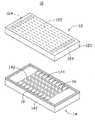
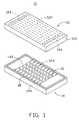
- FIG. 1is an exploded, isometric view of a touch panel in accordance with a present embodiment, showing a first electrode plate thereof inverted.
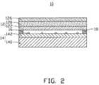
- FIG. 2is a side cross-sectional view of the touch panel of FIG. 1 once assembled.
- FIG. 3shows a Scanning Electron Microscope (SEM) image of a carbon nanotube wire-like structure used in the touch panel of FIG. 1 .
- FIG. 4shows a Scanning Electron Microscope (SEM) image of a carbon nanotube film.
- FIG. 5is a structural schematic of a carbon nanotube segment.
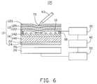
- FIG. 6is essentially a schematic cross-sectional view of the touch panel of the present embodiment used with a display element of a display device, showing operation of the touch panel with a touch tool.
- a touch panel 10includes a first electrode plate 12 , a second electrode plate 14 , and a plurality of dot spacers 16 located between the first electrode plate 12 and the second electrode plate 14 .
- the first electrode plate 12includes a first substrate 120 , a first conductive layer 122 , and at least two first-electrodes 124 .
- the first substrate 120has an upper surface and a lower surface, and the upper surface and the lower surface are substantially flat. In the illustrated embodiment, there are multiple first-electrodes 124 .
- the first-electrodes 124 and the first conductive layer 122are located on the lower surface of the first substrate 120 .
- the first-electrodes 124are arranged in two parallel columns at opposite ends of the lower surface of the first substrate 120 , and are electrically connected with the first conductive layer 122 .
- the first conductive layer 122is arranged on the lower surface of the first substrate 120 .
- first-electrodes 124are located at opposite ends of the first conductive layer 122 respectively.
- a direction from one of the columns of first-electrodes 124 across the first conductive layer 122 to the other column of first-electrodes 124is defined as a first direction.
- the second electrode plate 14includes a second substrate 140 , a second conductive layer 142 , and at least two second-electrodes 144 .
- the second substrate 140includes an upper surface and a lower surface, and the upper surface and the lower surface are substantially flat. In the illustrated embodiment, there are multiple second-electrodes 144 .
- the second-electrodes 144 and the second conductive layer 142are located on the upper surface of the second substrate 140 .
- the second-electrodes 144are arranged in two parallel columns at opposite ends of the upper surface of the second substrate 140 respectively, and are electrically connected with the second conductive layer 142 .
- the second conductive layer 142is arranged on a major portion of the upper surface of the second substrate 140 .
- the two columns of second-electrodes 144are located at opposite ends of the second conductive layer 142 respectively.
- a direction from one of the columns of second-electrodes 144 across the second conductive layer 142 to the other column of second-electrodes 144is defined as a second direction.
- the first directionis perpendicular to the second direction; i.e., the columns of first-electrodes 124 are orthogonal to the columns of second-electrodes 144 .
- the first substrate 120is a transparent and flexible film/plate.
- the second substrate 140is a transparent plate.
- the first-electrodes 124 and the second-electrodes 144are made of metal or any other suitable conductive material.
- the first substrate 120is a polyester film
- the second substrate 140is a glass plate
- the first-electrodes 124 and the second-electrodes 144are made of a conductive silver paste.
- An insulative layer 18is provided between the first and second substrates 120 , 140 .
- the insulative layer 18is in the form of a rectangular bead.
- the first electrode plate 12is located on the insulative layer 18 . That is, the first conductive layer 122 faces, but is spaced from, the second conductive layer 142 .
- the dot spacers 16are located on the second conductive layer 142 .
- a distance between the second electrode plate 14 and the first electrode plate 12is typically in an approximate range from 2 to 20 microns.
- the insulative layer 18 and the dot spacers 16are made of, for example, insulative resin or any other suitable insulative material. Electrical insulation between the first electrode plate 12 and the second electrode plate 14 is provided by the insulative layer 18 and the dot spacers 16 . It is to be understood that the dot spacers 16 are optional, particularly when the size of the touch panel 10 is relatively small.
- a transparent protective film 126is located on the upper surface of the first electrode plate 12 .
- the material of the transparent protective film 126can be selected from a group consisting of silicon nitrides, silicon dioxides, benzocyclobutenes, polyester films, and polyethylene terephthalates.
- the transparent protective film 126can be made of slick plastic and receive a surface hardening treatment to protect the first electrode plate 12 from being scratched when in use.
- At least one of the first conductive layer 122 and the second conductive layer 142includes a plurality of carbon nanotube wire-like structures.
- a plurality of the first-electrodes 124 and/or the second-electrodes 144is located on opposite ends of the corresponding electrode plate 12 , 14 having the plurality of carbon nanotube wire-like structures formed thereon.
- Two ends of each carbon nanotube wire-like structureare connected with two opposite first-electrodes 124 and/or second-electrodes 144 respectively. That is, each corresponding first-electrode 124 and/or second-electrode 144 is connected with the end of at least one carbon nanotube wire-like structure.
- the carbon nanotube wire-like structurecan be a carbon nanotube wire.
- each carbon nanotube wireis comprised of a plurality of successive carbon nanotubes joined end to end by van der Waals attractive force therebetween. Lengths of the carbon nanotube wires can be arbitrarily set as desired.
- the carbon nanotube wirescan be parallel to and spaced apart from each other.
- a diameter of each carbon nanotube wireis in an approximate range from 0.5 nanometers to 100 micrometers ( ⁇ m). Distances between adjacent carbon nanotube wires are in an approximate range from 10 nanometers to 1 millimeter.
- the carbon nanotubes in the carbon nanotube wirescan be selected from a group consisting of single-walled, double-walled, and multi-walled carbon nanotubes.
- a diameter of each single-walled carbon nanotubeis in an approximate range from 0.5 nanometers to 50 nanometers.
- a diameter of each double-walled carbon nanotubeis in an approximate range from 1 nanometer to 50 nanometers.
- a diameter of each multi-walled carbon nanotubeis in an approximate range from 1.5 nanometers to 50 nanometers.
- the first conductive layer 122 and the second conductive layer 142both include a plurality of carbon nanotube wire-like structures.
- the carbon nanotube wire-like structureis a carbon nanotube wire.
- the carbon nanotube wiresare parallel to each other and spaced apart from each other.
- the carbon nanotube wires in the first conductive layer 122cross the carbon nanotube wires in the second conductive layer 142 . That is, the carbon nanotube wires in the first conductive layer 122 are aligned along the first direction, and the carbon nanotube wires in the second conductive layer 142 are aligned along the second direction.
- the first directionis perpendicular to the second direction. In other embodiments, the first direction can be set at an angle other than perpendicular (oblique) to the second direction.
- a method for fabricating the above-described first conductive layer 122 and second conductive layer 142includes the steps of: (a) providing an array of carbon nanotubes or providing a super-aligned array of carbon nanotubes; (b) pulling out a carbon nanotube structure from the array of carbon nanotubes, by using a tool (e.g., adhesive tape, pliers, tweezers, or another tool allowing multiple carbon nanotubes to be gripped and pulled simultaneously); and (c) treating the carbon nanotube structure with an organic solvent or mechanical force to form a carbon nanotube wire; and (d) placing a plurality of the carbon nanotube wires in parallel and space apart from one another on each of the first substrate 120 and the second substrate 140 , thereby forming a first conductive layer 122 on the first substrate 120 and a second conductive layer 142 on the second substrate 140 .
- a toole.g., adhesive tape, pliers, tweezers, or another tool allowing multiple carbon nanotubes to be gripped and pulled
- the method of fabricating a nanotube filmcomprises steps (a) and (b).
- a nanotube filmcan be used as a shielding layer.
- a given super-aligned array of carbon nanotubescan be formed by the substeps of: (a 1 ) providing a substantially flat and smooth substrate; (a 2 ) forming a catalyst layer on the substrate; (a 3 ) annealing the substrate with the catalyst layer in air at a temperature in an approximate range from 700° C. to 900° C. for about 30 to 90 minutes; (a 4 ) heating the substrate with the catalyst layer to a temperature in the approximate range from 500° C. to 740° C. in a furnace with a protective gas therein; and (a 5 ) supplying a carbon source gas to the furnace for about 5 to 30 minutes and growing the super-aligned array of carbon nanotubes on the substrate.
- the substratecan be a P-type silicon wafer, an N-type silicon wafer, or a silicon wafer with a film of silicon dioxide thereon.
- a 4-inch P-type silicon waferis used as the substrate.
- the catalystcan be made of iron (Fe), cobalt (Co), nickel (Ni), or any alloy thereof.
- the protective gascan be made up of at least one of nitrogen (N2), ammonia (NH3), and a noble gas.
- the carbon source gascan be a hydrocarbon gas, such as ethylene (C2H4), methane (CH4), acetylene (C2H2), ethane (C2H6), or any combination thereof.
- the super-aligned array of carbon nanotubescan have a height of about 50 microns to 5 millimeters and include a plurality of carbon nanotubes parallel to each other and approximately perpendicular to the substrate.
- the carbon nanotubes in the array of carbon nanotubescan be selected from a group consisting of single-walled carbon nanotubes, double-walled carbon nanotubes, and multi-walled carbon nanotubes.
- a diameter of each single-walled carbon nanotubeapproximately ranges from 0.5 nanometers to 50 nanometers.
- a diameter of each double-walled carbon nanotubeapproximately ranges from 1 nanometer to 50 nanometers.
- a diameter of each multi-walled carbon nanotubeapproximately ranges from 1.5 nanometers to 50 nanometers.
- the super-aligned array of carbon nanotubes formed under the above conditionsis essentially free of impurities such as carbonaceous or residual catalyst particles.
- the carbon nanotubes in the super-aligned arrayare closely packed together by the van der Waals attractive force.
- the carbon nanotube structurecan be formed by the substeps of: (b 1 ) selecting a plurality of carbon nanotube segments having a predetermined width from the array of carbon nanotubes; and (b 2 ) pulling the carbon nanotube segments at an even/uniform speed to achieve a uniform carbon nanotube structure.
- each carbon nanotube segment 143includes a plurality of carbon nanotubes 145 parallel to each other, and combined by van der Waals attractive force therebetween.
- the carbon nanotube segments 145can vary in width, thickness, uniformity and shape.
- the pulling directionis substantially perpendicular to the growing direction of the super-aligned array of carbon nanotubes.
- step (c)the carbon nanotube structure is soaked in an organic solvent. Since the untreated carbon nanotube structure is composed of a number of carbon nanotubes 145 , the untreated carbon nanotube structure has a high surface area to volume ratio and thus may easily become stuck to other objects. During the surface treatment, the carbon nanotube structure is shrunk into a carbon nanotube wire after the organic solvent volatilizing, due to factors such as surface tension. The surface area to volume ratio and diameter of the treated carbon nanotube wire is reduced. Accordingly, the stickiness of the carbon nanotube structure is lowered, and strength and toughness of the carbon nanotube structure is improved.
- the organic solventmay be a volatilizable organic solvent, such as ethanol, methanol, acetone, dichloroethane, chloroform, and any combination thereof.
- a diameter of the carbon nanotube wiresapproximately ranges from 0.5 nanometers to 100 micrometers ( ⁇ m).
- the carbon nanotube structurealso can be treated with mechanical force (e.g., a conventional spinning process), to acquire a carbon nanotube wire in a twisted shape.
- mechanical forcee.g., a conventional spinning process
- the distances between the adjacent carbon nanotube wirescan be set according to the desired optical transparency properties of the touch panel 10 .
- the distances between the adjacent carbon nanotube wiresare in an approximate range from 10 nanometers to 1 millimeter. Further, all the adjacent carbon nanotube wires are spaced apart a same distance.
- each of the carbon nanotube wires in the first conductive layer 122are connected with two corresponding opposite first-electrodes 124
- two ends of each of the carbon nanotube wires in the second conductive layer 142are connected with two corresponding opposite second-electrodes 144 .
- Each first-electrode 124 and second-electrode 144is connected with the end of at least one carbon nanotube wire.
- each first-electrode 124is connected with the end of only one carbon nanotube wire in the first conductive layer 122
- each second-electrode 144is connected with the end of only one carbon nanotube wire in the second conductive layer 142 .
- the carbon nanotube wires in the first conductive layer 122are spaced apart, and each carbon nanotube wire is arranged along the first direction.
- each carbon nanotube wire in the first conductive layer 122can stray from the first direction.
- the carbon nanotube wires in the second conductive layer 142are spaced apart, and each carbon nanotube wire is arranged along the second direction.
- the first directionis perpendicular to the second direction.
- each carbon nanotube wire in the second conductive layer 142can deflect from the second direction.
- the plurality of first-electrodes 124 and second-electrodes 144are connected with a circuit of the touch panel 10 via electrode down-leads.
- the touch panel 10can further include a shielding layer 22 located on the lower surface of the second substrate 140 .
- the material of the shielding layer 22can be selected from a group consisting of indium tin oxides, antimony tin oxides, carbon nanotube films, and other conductive materials.
- the shielding layer 22is a carbon nanotube film.
- the carbon nanotube filmincludes a plurality of carbon nanotubes, and the orientations of the carbon nanotubes therein can be arbitrarily set as desired.
- the carbon nanotubes in the carbon nanotube film of the shielding layer 22are arranged along a same direction.
- the carbon nanotube filmis connected to ground and acts as a shield, thus enabling the touch panel 10 to operate without interference (e.g., electromagnetic interference).
- An exemplary display device 100includes the touch panel 10 , a display element 20 , a first controller 30 , a central processing unit (CPU) 40 , and a second controller 50 .
- the touch panel 10is opposite and adjacent to the display element 20 , and is connected to the first controller 30 by a circuit external to the touch panel 10 .
- the touch panel 10can be spaced from the display element 20 or installed directly on the display element 20 .
- the touch panel 10is spaced from the display element 20 . That is, the touch panel 10 and the display element 20 are spaced apart and separated by a gap 26 .
- the first controller 30 , the CPU 40 , and the second controller 50are electrically connected.
- the CPU 40is connected to the second controller 50 to control the display element 20 .
- the display element 20can be, e.g., a liquid crystal display, a field emission display, a plasma display, an electroluminescent display, a vacuum fluorescent display, a cathode ray tube, or another display device.
- a passivation layer 24is located on a surface of the shielding layer 22 that faces away from the second substrate 140 .
- the material of the passivation layer 24can, for example, be silicon nitride or silicon dioxide.
- the passivation layer 24can protect the shielding layer 22 from chemical or mechanical damage.
- a 5V (volts) voltageis applied to the two columns of first-electrodes 124 of the first electrode plate 12 , and to the two columns of second-electrodes 144 of the second electrode plate 14 .
- a useroperates the display device 100 by pressing the first electrode plate 12 of the touch panel 10 with a finger 60 , a pen/stylus 60 , or the like, while visually observing the display element 20 through the touch panel 10 .
- This pressingcauses a deformation 70 of the first electrode plate 12 .
- the deformation 70 of the first electrode plate 12establishes an electrical connection between the first conductive layer 122 of the first electrode plate 12 and the second conductive layer 142 of the second electrode plate 14 .
- Changes in voltages along the first direction of the first conductive layer 122 and along the second direction of the second conductive layer 142can be detected by the first controller 30 . Then the first controller 30 transforms the changes in voltages into coordinates of the pressing point, and sends the coordinates to the CPU 40 . The CPU 40 then sends out commands according to the coordinates of the pressing point. Thereby, the user can control the display of the display element 20 .
- the properties of the carbon nanotubesprovide superior toughness, high mechanical strength, and uniform conductivity to the carbon nanotube wire-like structures derived from the carbon nanotube films and/or yarns.
- the touch panel 10 and the display device 100 adopting the carbon nanotube wire-like structures as the first and second conductive layers 122 , 142are durable and highly conductive.
- each of the first and second conductive layers 122 , 142 formed by the plurality of spaced-apart carbon nanotube wire-like structures parallel to each otherhas a uniform resistance distribution and uniform optical transparency.
- the touch panel 10 and the display device 100 adopting the carbon nanotube wire-like structureshave improved sensitivity and accuracy.
- each first-electrode 124 and second-electrode 144is connected with the end of at least one corresponding carbon nanotube wire-like structure, the determination of the position of the pressing point by detecting the voltage changes between the corresponding pairs of opposite electrodes 124 , 144 can be highly accurate. That is, the touch panel 10 and the display device 100 can provide operation with very high precision.
Landscapes
- Engineering & Computer Science (AREA)
- General Engineering & Computer Science (AREA)
- Theoretical Computer Science (AREA)
- Human Computer Interaction (AREA)
- Physics & Mathematics (AREA)
- General Physics & Mathematics (AREA)
- Position Input By Displaying (AREA)
Abstract
Description
Claims (19)
Applications Claiming Priority (3)
| Application Number | Priority Date | Filing Date | Title |
|---|---|---|---|
| CN200710125409 | 2007-12-21 | ||
| CN200710125409.6 | 2007-12-21 | ||
| CN2007101254096ACN101464765B (en) | 2007-12-21 | 2007-12-21 | Touch screen and display equipment |
Publications (2)
| Publication Number | Publication Date |
|---|---|
| US20090160798A1 US20090160798A1 (en) | 2009-06-25 |
| US8325146B2true US8325146B2 (en) | 2012-12-04 |
Family
ID=40788015
Family Applications (1)
| Application Number | Title | Priority Date | Filing Date |
|---|---|---|---|
| US12/286,184Active2030-08-22US8325146B2 (en) | 2007-12-21 | 2008-09-29 | Touch panel and display device using the same |
Country Status (3)
| Country | Link |
|---|---|
| US (1) | US8325146B2 (en) |
| JP (1) | JP2009151783A (en) |
| CN (1) | CN101464765B (en) |
Cited By (2)
| Publication number | Priority date | Publication date | Assignee | Title |
|---|---|---|---|---|
| US20100133569A1 (en)* | 2008-11-28 | 2010-06-03 | Tsinghua University | Light emitting diode |
| US20150346878A1 (en)* | 2014-05-30 | 2015-12-03 | Tpk Touch Solutions Inc. | Touch module and manufacturing method thereof |
Families Citing this family (25)
| Publication number | Priority date | Publication date | Assignee | Title |
|---|---|---|---|---|
| CN101937279B (en)* | 2009-06-30 | 2013-11-13 | 群康科技(深圳)有限公司 | Touch screen and driving method thereof |
| CN101950213B (en)* | 2009-07-10 | 2013-05-22 | 群康科技(深圳)有限公司 | Touch screen and multi-point identification method used for same |
| CN101950231B (en)* | 2009-07-10 | 2012-10-24 | 群康科技(深圳)有限公司 | Method for detecting touching position for touch device |
| TWI469029B (en)* | 2009-07-15 | 2015-01-11 | Chimei Innolux Corp | Method for detecting a touched position on a touch device |
| CN101963855B (en)* | 2009-07-24 | 2012-11-21 | 群康科技(深圳)有限公司 | Multi-point touch identification method for touch screen |
| FI127197B (en)* | 2009-09-04 | 2018-01-31 | Canatu Oy | Touch screen and method of manufacturing a touch screen |
| CN102033669B (en)* | 2009-09-24 | 2013-08-14 | 群康科技(深圳)有限公司 | Capacitance-type touch panel |
| TWI412819B (en)* | 2009-10-09 | 2013-10-21 | Innolux Corp | Capacitive touch panel |
| CN102053409B (en)* | 2009-11-02 | 2015-06-10 | 北京富纳特创新科技有限公司 | Display device |
| CN102193692B (en)* | 2010-03-03 | 2014-09-10 | 群康科技(深圳)有限公司 | Surface capacitive touch panel and display device, electronic device as well as driving method thereof |
| CN101825796B (en) | 2010-05-19 | 2012-06-13 | 北京富纳特创新科技有限公司 | Touch liquid crystal screen |
| CN101852934A (en) | 2010-05-31 | 2010-10-06 | 北京富纳特创新科技有限公司 | Touch type liquid crystal display screen |
| CN101852935A (en) | 2010-06-02 | 2010-10-06 | 北京富纳特创新科技有限公司 | Touch liquid crystal display |
| KR20110136181A (en)* | 2010-06-14 | 2011-12-21 | 삼성전자주식회사 | Touch panel, display device including same, and manufacturing method thereof |
| CN101880035A (en) | 2010-06-29 | 2010-11-10 | 清华大学 | carbon nanotube structure |
| CN102402319B (en)* | 2010-09-09 | 2014-09-24 | 群康科技(深圳)有限公司 | Method and device for driving touch panel |
| TWI455001B (en)* | 2010-09-21 | 2014-10-01 | Innolux Corp | Method and apparatus for driving touch panel |
| CN102622091B (en) | 2011-01-28 | 2015-11-25 | 清华大学 | Flexible keyboard |
| CN102622089B (en)* | 2011-01-28 | 2016-03-30 | 清华大学 | Flexible keyboard |
| CN102566190A (en)* | 2011-12-23 | 2012-07-11 | 鸿富锦精密工业(深圳)有限公司 | Electronic paper device |
| CN105807971B (en)* | 2014-12-31 | 2019-01-18 | 清华大学 | Electrostatic transducer |
| CN105807970B (en)* | 2014-12-31 | 2018-08-17 | 清华大学 | Hovering control device |
| CN105807973B (en)* | 2014-12-31 | 2019-01-18 | 清华大学 | Electrostatic transducer |
| EP3263331B1 (en)* | 2015-02-23 | 2022-03-30 | Lintec of America, Inc. | Adhesive sheet |
| KR101809369B1 (en)* | 2016-06-10 | 2017-12-15 | 한양대학교 산학협력단 | Conductive Structure, Manufacturing Method thereof, Touch Sensor comprising the Conductive Structure, Manufacturing Method for the Touch sensor and Touch Sensing Method |
Citations (176)
| Publication number | Priority date | Publication date | Assignee | Title |
|---|---|---|---|---|
| JPS61231626A (en) | 1985-04-05 | 1986-10-15 | Asahi Chem Ind Co Ltd | Conductive sheet for position detection |
| JPS6263332U (en) | 1985-10-11 | 1987-04-20 | ||
| US4659873A (en) | 1985-07-19 | 1987-04-21 | Elographics, Inc. | Fabric touch sensor and method of manufacture |
| JPS62182916U (en) | 1986-05-08 | 1987-11-20 | ||
| JPS62190524U (en) | 1986-05-26 | 1987-12-04 | ||
| US4922061A (en) | 1988-06-13 | 1990-05-01 | Tektronix, Inc. | Capacitive touch panel system with randomly modulated position measurement signal |
| US4933660A (en) | 1989-10-27 | 1990-06-12 | Elographics, Inc. | Touch sensor with touch pressure capability |
| US5181030A (en) | 1989-12-28 | 1993-01-19 | Gunze Limited | Input system including resistance film touch panel and pushed position detecting device |
| JPH0628090Y2 (en) | 1992-06-03 | 1994-08-03 | 健一 古谷 | Electrode structure in used needle processing equipment |
| TW242732B (en) | 1993-06-29 | 1995-03-11 | Victor Company Of Japan | Digital chrominance signal processing circuit |
| TW284963B (en) | 1995-02-17 | 1996-09-01 | Nippon Tobacco Sangyo Kk | |
| TW284927B (en) | 1993-05-27 | 1996-09-01 | Mabuchi Motor Co | |
| JPH1063404A (en) | 1996-08-27 | 1998-03-06 | Matsushita Electric Ind Co Ltd | Coordinate position input device |
| TW341684B (en) | 1996-07-15 | 1998-10-01 | Synaptics Inc | Object position detector |
| US5853877A (en) | 1996-05-31 | 1998-12-29 | Hyperion Catalysis International, Inc. | Method for disentangling hollow carbon microfibers, electrically conductive transparent carbon microfibers aggregation film amd coating for forming such film |
| US5861583A (en) | 1992-06-08 | 1999-01-19 | Synaptics, Incorporated | Object position detector |
| US5931764A (en) | 1998-06-24 | 1999-08-03 | Viztec, Inc. | Wearable device with flexible display |
| JP2001267782A (en) | 2000-03-21 | 2001-09-28 | Shimadzu Corp | Electromagnetic wave absorption shielding material |
| US6373472B1 (en) | 1995-10-13 | 2002-04-16 | Silviu Palalau | Driver control interface system |
| US20020089492A1 (en) | 2001-01-11 | 2002-07-11 | Young-Soo Ahn | Flat panel display with input device |
| US6423583B1 (en) | 2001-01-03 | 2002-07-23 | International Business Machines Corporation | Methodology for electrically induced selective breakdown of nanotubes |
| TW498266B (en) | 2000-08-03 | 2002-08-11 | Hantouch Com | Resistive film type transparent analog touch panel |
| JP2002278701A (en) | 2001-03-21 | 2002-09-27 | Nissha Printing Co Ltd | Touch panel |
| WO2002076724A1 (en) | 2001-03-26 | 2002-10-03 | Eikos, Inc. | Coatings containing carbon nanotubes |
| TW508652B (en) | 2001-10-03 | 2002-11-01 | Taiwan Semiconductor Mfg | Device and method for wafer drying |
| TW521227B (en) | 2000-03-31 | 2003-02-21 | Sharp Kk | Electrode substrate, method for producing the same and display device including the same |
| CN2539375Y (en) | 2002-04-15 | 2003-03-05 | 湖南三才光电信息材料有限公司 | High-stable flexible transparent conducting composite film |
| US20030122800A1 (en) | 2001-12-27 | 2003-07-03 | Lg, Philips Lcd Co., Ltd. | Touch panel liquid crystal display device and method of fabricating the same |
| US20030147041A1 (en) | 2001-12-27 | 2003-08-07 | Lg.Philips Lcd Co., Ltd | Method of fabricating liquid crystal display apparatus integrated with film type touch panel |
| US6628269B2 (en) | 2000-02-10 | 2003-09-30 | Nec Corporation | Touch panel input device capable of sensing input operation using a pen and a fingertip and method therefore |
| US6629833B1 (en) | 1998-05-15 | 2003-10-07 | Toyo Boseki Kabushiki Kaisha | Transparent conductive film and touch panel |
| CN1447279A (en) | 2003-03-18 | 2003-10-08 | 中国电子科技集团公司第五十五研究所 | High reliable touch screen and manufacturing technique |
| US20030189235A1 (en) | 2002-04-09 | 2003-10-09 | Hiroyuki Watanabe | Photoelectric conversion element and photoelectric conversion device |
| TW200403498A (en) | 2002-08-20 | 2004-03-01 | Samsung Electronics Co Ltd | Light guide plate and liquid crystal display having the same |
| US20040047038A1 (en) | 2002-09-10 | 2004-03-11 | Kai-Li Jiang | Optical polarizer and method for fabricating such optical polarizer |
| US20040053780A1 (en) | 2002-09-16 | 2004-03-18 | Jiang Kaili | Method for fabricating carbon nanotube yarn |
| US20040099438A1 (en) | 2002-05-21 | 2004-05-27 | Arthur David J. | Method for patterning carbon nanotube coating and carbon nanotube wiring |
| CN1501317A (en) | 2002-11-14 | 2004-06-02 | Lg.������Lcd����˾ | display device touch screen |
| CN1503195A (en) | 2002-11-20 | 2004-06-09 | Lg.������Lcd��ʽ���� | Digital Resistive Touch Panel |
| CN1509982A (en) | 2002-12-21 | 2004-07-07 | �廪��ѧ | A carbon nanotube array structure and its growth method |
| JP2004189573A (en) | 2002-12-13 | 2004-07-08 | Jfe Engineering Kk | Aggregate of carbon nanotubes and carbon nanotube installation device having the same |
| CN1519196A (en) | 2003-01-23 | 2004-08-11 | 南昌大学 | Fabrication method of aligned carbon nanotube film on soft substrate |
| CN2638143Y (en) | 2003-05-24 | 2004-09-01 | 江阴市华丽计算机网络工程有限公司 | Multifunctional PDA |
| JP2004253796A (en) | 2003-01-31 | 2004-09-09 | Takiron Co Ltd | Electromagnetic wave shielding structure |
| JP2004266272A (en) | 2003-02-14 | 2004-09-24 | Toray Ind Inc | Field effect transistor and liquid crystal display device using the same |
| US20040191157A1 (en) | 2003-03-31 | 2004-09-30 | Avetik Harutyunyan | Method for selective enrichment of carbon nanotubes |
| US20040251504A1 (en) | 2003-05-07 | 2004-12-16 | Sony Corporation | Field effect transistor and method for manufacturing the same |
| US20050110720A1 (en) | 2003-11-21 | 2005-05-26 | Hitachi Displays, Ltd. | Image display device |
| TWI233570B (en) | 2001-12-28 | 2005-06-01 | Lg Philips Lcd Co Ltd | Touch panel display apparatus and method of fabricating the same |
| CN2706973Y (en) | 2004-06-30 | 2005-06-29 | 陈凯 | Fingers-nipping gloves cell phone |
| JP2005176428A (en) | 2003-12-08 | 2005-06-30 | Japan Science & Technology Agency | Actuator element |
| TW200522366A (en) | 2003-11-19 | 2005-07-01 | Seiko Epson Corp | Method of manufacturing a thin film transistor, thin film transistor, thin film transistor circuit, electronic device, and electronic apparatus |
| JP2005182339A (en) | 2003-12-18 | 2005-07-07 | Kawaguchiko Seimitsu Co Ltd | Touch panel and screen input type display device therewith |
| JP2005222182A (en) | 2004-02-04 | 2005-08-18 | Citizen Watch Co Ltd | Position inputting device |
| US6947203B2 (en) | 2003-06-24 | 2005-09-20 | Seiko Epson Corporation | Electrophoretic dispersion, electrophoretic display device, method of manufacturing electrophoretic display device, and electronic system |
| US20050209392A1 (en) | 2003-12-17 | 2005-09-22 | Jiazhong Luo | Polymer binders for flexible and transparent conductive coatings containing carbon nanotubes |
| JP2005286158A (en) | 2004-03-30 | 2005-10-13 | Seiko Epson Corp | PATTERN FORMING METHOD, ELECTRONIC DEVICE, ITS MANUFACTURING METHOD, AND ELECTRONIC DEVICE |
| CN1690915A (en) | 2004-04-28 | 2005-11-02 | 秦建忠 | Double screen notebook computer |
| WO2005104141A1 (en) | 2004-04-20 | 2005-11-03 | Takiron Co., Ltd. | Touch panel-use transparent conductive molded product and touch panel |
| WO2005102924A1 (en) | 2004-04-19 | 2005-11-03 | Japan Science And Technology Agency | Carbon-based fine structure group, aggregate of carbon based fine structures, use thereof and method for preparation thereof |
| WO2006003245A1 (en) | 2004-07-06 | 2006-01-12 | Upm-Kymmene Corporation | Sensor product for electric field sensing |
| US20060010996A1 (en) | 2004-07-13 | 2006-01-19 | United States Of America As Represented By The Administrator Of The Nasa | Carbon nanotube-based sensor and method for continually sensing changes in a structure |
| US20060022221A1 (en) | 2004-07-29 | 2006-02-02 | International Business Machines Corporation | Integrated circuit chip utilizing oriented carbon nanotube conductive layers |
| TWI249134B (en) | 2003-07-23 | 2006-02-11 | Wintek Corp | Touch panel structure |
| TWI249708B (en) | 2004-09-09 | 2006-02-21 | Ind Tech Res Inst | Analog resistive touch panel without bias |
| CN1738018A (en) | 2005-08-18 | 2006-02-22 | 上海交通大学 | Method for Bonding Nanomaterials to Metal Electrodes |
| US20060044284A1 (en) | 2004-09-02 | 2006-03-02 | Koji Tanabe | Touch panel and the manufacturing method |
| CN1745302A (en) | 2003-01-30 | 2006-03-08 | 艾考斯公司 | Articles with dispersed conductive coatings |
| WO2006030981A1 (en) | 2004-09-17 | 2006-03-23 | National Institute Of Advanced Industrial Scienceand Technology | Transparent conductive carbon nanotube film and method for producing same |
| US20060077147A1 (en) | 2004-09-27 | 2006-04-13 | Lauren Palmateer | System and method for protecting micro-structure of display array using spacers in gap within display device |
| TWI253846B (en) | 2005-03-28 | 2006-04-21 | Ind Tech Res Inst | Photo-sensing display unit |
| US20060097991A1 (en) | 2004-05-06 | 2006-05-11 | Apple Computer, Inc. | Multipoint touchscreen |
| JP2006171336A (en) | 2004-12-15 | 2006-06-29 | Takiron Co Ltd | Transparent electrode member for image display, and the image display device |
| TW200622432A (en) | 2004-12-31 | 2006-07-01 | Hon Hai Prec Ind Co Ltd | Liquid crystal display device |
| US7071927B2 (en) | 1999-11-17 | 2006-07-04 | L-3 Communications Corporation | Resistive touch panel using removable, tensioned top layer |
| CN1803594A (en) | 2005-11-25 | 2006-07-19 | 清华大学 | Large-area ultra-thin carbon nanotube film and its preparation process |
| TWI258708B (en) | 2005-01-27 | 2006-07-21 | Apex Material Technology Corp | Resistive touch panel, and it manufacturing method |
| US20060171032A1 (en) | 2005-01-07 | 2006-08-03 | Kimihiko Nishioka | Medium exhibiting negative refraction, optical element, and optical system |
| CN1823320A (en) | 2003-06-14 | 2006-08-23 | 罗纳德·P·宾斯蒂德 | Improvements in touch technology |
| US20060187369A1 (en) | 2004-05-13 | 2006-08-24 | Quanta Display Inc. | Liquid crystal display without storage capacitance electrode lines |
| US20060188721A1 (en) | 2005-02-22 | 2006-08-24 | Eastman Kodak Company | Adhesive transfer method of carbon nanotube layer |
| US20060187213A1 (en) | 2005-02-21 | 2006-08-24 | Au Optronics Corp. | Electroluminescence display with touch panel |
| JP2006228818A (en) | 2005-02-15 | 2006-08-31 | Fujitsu Ltd | Method for forming carbon nanotube and method for manufacturing electronic device |
| JP2006243455A (en) | 2005-03-04 | 2006-09-14 | C's Lab Ltd | Map display method, map display program, and map display device |
| US20060213251A1 (en) | 2005-03-24 | 2006-09-28 | University Of Florida Research Foundation, Inc. | Carbon nanotube films for hydrogen sensing |
| JP2006269311A (en) | 2005-03-25 | 2006-10-05 | Toray Ind Inc | Transparent conductive film containing carbon nano-tube obtained by making metal-carrying carrier contact with carbon-containing organic compound |
| JP2006285068A (en) | 2005-04-04 | 2006-10-19 | Nikkiso Co Ltd | Conductive polarizing film |
| US20060240605A1 (en) | 2005-04-22 | 2006-10-26 | Hee-Sung Moon | Organic thin film transistor and method of fabricating the same |
| WO2006120803A1 (en) | 2005-05-10 | 2006-11-16 | Sumitomo Precision Products Co., Ltd | Highly thermally conductive composite material |
| US20060262055A1 (en) | 2005-01-26 | 2006-11-23 | Toshiba Matsushita Display Technology | Plane display device |
| US20060263588A1 (en) | 2005-04-28 | 2006-11-23 | Bussan Nanotech Research Institute Inc. | Transparent conductive film and coating composition therefor |
| WO2006126604A1 (en) | 2005-05-26 | 2006-11-30 | Gunze Limited | Transparent planar body and transparent touch switch |
| CN2844974Y (en) | 2005-12-08 | 2006-12-06 | 比亚迪股份有限公司 | Contact style liquid crystal display device |
| US20060274049A1 (en) | 2005-06-02 | 2006-12-07 | Eastman Kodak Company | Multi-layer conductor with carbon nanotubes |
| US20060274047A1 (en) | 2005-06-02 | 2006-12-07 | Eastman Kodak Company | Touchscreen with one carbon nanotube conductive layer |
| US20060275956A1 (en) | 2005-06-04 | 2006-12-07 | Gregory Konesky | Cross-linked carbon nanotubes |
| US20060274048A1 (en) | 2005-06-02 | 2006-12-07 | Eastman Kodak Company | Touchscreen with conductive layer comprising carbon nanotubes |
| KR20060129977A (en) | 2006-09-08 | 2006-12-18 | 아이티엠 주식회사 | Highly durable resistive touch screen panel and its manufacturing method |
| CN1903793A (en) | 2005-07-26 | 2007-01-31 | 中国科学院物理研究所 | Carbon silicon composite material, its preparation method and use |
| WO2007012899A1 (en) | 2005-07-25 | 2007-02-01 | Plastic Logic Limited | Flexible touch screen display |
| TWM306694U (en) | 2006-03-15 | 2007-02-21 | Ushine Photonics Corp | Durable resistive touch screen |
| TW200710493A (en) | 2005-05-23 | 2007-03-16 | Ran-Hong Wang | Controlling polarization for liquid crystal displays |
| US7196463B2 (en)* | 2003-08-06 | 2007-03-27 | Hitachi Displays, Ltd. | Emissive flat panel display having electron sources with high current density and low electric field strength |
| TW200713337A (en) | 2005-07-07 | 2007-04-01 | 3M Innovative Properties Co | Touch panel sensor |
| US20070075619A1 (en) | 2005-09-30 | 2007-04-05 | Tsinghua University | Field emission device and method for making the same |
| US20070081681A1 (en) | 2005-10-03 | 2007-04-12 | Xun Yu | Thin film transparent acoustic transducer |
| CN1948144A (en) | 2006-11-10 | 2007-04-18 | 清华大学 | Ultralong orientational carbon nano-tube filament/film and its preparation method |
| US20070085838A1 (en) | 2005-10-17 | 2007-04-19 | Ricks Theodore K | Method for making a display with integrated touchscreen |
| TW200717083A (en) | 2005-10-28 | 2007-05-01 | Hon Hai Prec Ind Co Ltd | Liquid crystal display and its manufacturing method |
| US20070099333A1 (en) | 2003-07-17 | 2007-05-03 | Seiko Epson Corporation | Thin-film transistor, method of producing thin-film transistor, electronic circuit, display, and electronic device |
| US7215329B2 (en) | 2001-10-10 | 2007-05-08 | Smk Corporation | Touch panel input device |
| CN1315362C (en) | 2003-06-27 | 2007-05-09 | 中国科学院上海硅酸盐研究所 | Carbon nano-pipe/ceramic composite material possessing microwave absorption function and its preparation method |
| JP2007112133A (en) | 2003-01-30 | 2007-05-10 | Takiron Co Ltd | Electroconductive shaped article |
| TW200719198A (en) | 2005-06-16 | 2007-05-16 | Nissha Printing | Housing component with illuminated switch and method of producing the same |
| JP2007123870A (en) | 2005-09-29 | 2007-05-17 | Matsushita Electric Ind Co Ltd | Flat panel display device and manufacturing method thereof |
| WO2007063751A1 (en) | 2005-11-29 | 2007-06-07 | Seiko Instruments Inc. | Process for producing display and method of laminating |
| WO2007066649A1 (en) | 2005-12-06 | 2007-06-14 | Mitsubishi Rayon Co., Ltd. | Carbon nanotube-containing composition, composite body, and their production methods |
| TW200722559A (en) | 2005-12-06 | 2007-06-16 | Ind Tech Res Inst | Metal nanodot arrays and fabrication methods thereof |
| CN1982209A (en) | 2005-12-16 | 2007-06-20 | 清华大学 | Carbon nano-tube filament and its production |
| WO2007022226A3 (en) | 2005-08-12 | 2007-06-21 | Cambrios Technologies Corp | Nanowires-based transparent conductors |
| JP2007161576A (en) | 2005-12-09 | 2007-06-28 | Kofukin Seimitsu Kogyo (Shenzhen) Yugenkoshi | Method for producing carbon nanotube array |
| US7242136B2 (en) | 2003-03-11 | 2007-07-10 | Lg Electronics Inc. | Front filter, and plasma display apparatus having the same |
| CN1996620A (en) | 2006-12-29 | 2007-07-11 | 清华大学 | Carbon nano tube film-based solar energy battery and its preparing method |
| TW200727163A (en) | 2006-01-06 | 2007-07-16 | Pan Jit Internat Inc | Antibacterial touch display device |
| US20070165004A1 (en) | 2006-01-17 | 2007-07-19 | World Properties, Inc. | Capacitive touch sensor with integral EL backlight |
| JP2007182546A (en) | 2005-12-06 | 2007-07-19 | Mitsubishi Rayon Co Ltd | Carbon nanotube-containing composition, composite, and production method thereof |
| JP2007182357A (en) | 2006-01-10 | 2007-07-19 | Nok Corp | Aftertreatment method of carbon material thin film |
| US20070182720A1 (en) | 2006-02-07 | 2007-08-09 | Shoji Fujii | Touch panel |
| KR20070081902A (en) | 2006-02-14 | 2007-08-20 | 삼성전자주식회사 | Liquid crystal display |
| DE202007006407U1 (en) | 2006-05-05 | 2007-09-06 | Philipp, Harald | Touch screen element |
| WO2007099975A1 (en) | 2006-02-28 | 2007-09-07 | Toyo Boseki Kabushiki Kaisha | Carbon nanotube assembly, carbon nanotube fiber and process for producing carbon nanotube fiber |
| JP2007229989A (en) | 2006-02-28 | 2007-09-13 | Takiron Co Ltd | Conductive molded body and its manufacturing method |
| US20070215841A1 (en) | 2004-05-14 | 2007-09-20 | Sonydeutschland Gmbh | Composite Materials Comprising Carbon Nanotubes and Metal Carbonates |
| TW200737414A (en) | 2006-03-23 | 2007-10-01 | Unimicron Technology Corp | Carbon nanotube field emitting display |
| TW200736979A (en) | 2006-03-17 | 2007-10-01 | Innolux Display Corp | Touch panel |
| TW200738558A (en) | 2006-01-03 | 2007-10-16 | Nano Proprietary Inc | Curing binder material for carbon nanotube electron emission cathodes |
| CN101059738A (en) | 2006-04-20 | 2007-10-24 | 铼宝科技股份有限公司 | Transparent touch screen with upward-emitting organic light-emitting diodes |
| JP2007310869A (en) | 2006-04-17 | 2007-11-29 | Matsushita Electric Ind Co Ltd | Input device control method and input device used therefor |
| US20070279556A1 (en) | 2005-05-23 | 2007-12-06 | Wang Ran-Hong R | Controlling polarization for liquid crystal displays |
| US20070296897A1 (en) | 2006-06-23 | 2007-12-27 | Tsinghua University | Liquid crystal cell assembly for liquid crystal display |
| US20080048996A1 (en) | 2006-08-11 | 2008-02-28 | Unidym, Inc. | Touch screen devices employing nanostructure networks |
| US7355592B2 (en) | 2002-12-24 | 2008-04-08 | Lg.Philips Lcd Co., Ltd. | Digital resistive type touch panel and fabrication method thereof |
| US20080088219A1 (en) | 2006-10-17 | 2008-04-17 | Samsung Electronics Co., Ltd. | Transparent carbon nanotube electrode using conductive dispersant and production method thereof |
| JP2008102968A (en) | 2007-12-28 | 2008-05-01 | Fujitsu Component Ltd | Touch panel |
| US20080129666A1 (en) | 2006-12-05 | 2008-06-05 | Susumu Shimotono | Method and Apparatus for Changing a Display Direction of a Screen of a Portable Electronic Device |
| US20080192014A1 (en)* | 2007-02-08 | 2008-08-14 | Tyco Electronics Corporation | Touch screen using carbon nanotube electrodes |
| US20080238882A1 (en) | 2007-02-21 | 2008-10-02 | Ramesh Sivarajan | Symmetric touch screen system with carbon nanotube-based transparent conductive electrode pairs |
| US20080248235A1 (en) | 2007-02-09 | 2008-10-09 | Tsinghua University | Carbon nanotube film structure and method for fabricating the same |
| US20080266273A1 (en) | 2007-04-24 | 2008-10-30 | White Electronic Designs Corp. | Interactive display system |
| US20090032777A1 (en) | 2005-06-07 | 2009-02-05 | Kuraray Co., Ltd. | Carbon nanotube dispersion liquid and transparent conductive film using same |
| US20090056854A1 (en) | 2006-04-04 | 2009-03-05 | Top-Nanosis, Inc. | Method for manufacturing conductive composite material |
| US20090059151A1 (en) | 2007-09-03 | 2009-03-05 | Samsung Electronics Co., Ltd. | Liquid crystal display panel and manufacturintg method therreof |
| US20090101488A1 (en) | 2007-10-23 | 2009-04-23 | Tsinghua University | Touch panel |
| JP2009104577A (en) | 2007-10-23 | 2009-05-14 | Kofukin Seimitsu Kogyo (Shenzhen) Yugenkoshi | Touch panel |
| US20090153511A1 (en) | 2007-12-12 | 2009-06-18 | Tsinghua University | Touch panel and display device using the same |
| US20090153513A1 (en) | 2007-12-14 | 2009-06-18 | Tsinghua University | Touch panel, method for making the same, and display device adopting the same |
| US20090153516A1 (en) | 2007-12-12 | 2009-06-18 | Tsinghua University | Touch panel, method for making the same, and display device adopting the same |
| TW200928914A (en) | 2007-12-31 | 2009-07-01 | Hon Hai Prec Ind Co Ltd | Touch panel and displaying device using the same |
| TW200929638A (en) | 2007-12-21 | 2009-07-01 | Hon Hai Prec Ind Co Ltd | Touch panel, method for making the same, and displaying device adopting the same |
| TW200929643A (en) | 2007-12-21 | 2009-07-01 | Hon Hai Prec Ind Co Ltd | Touch panel, method for making the same, and displaying device adopting the same |
| US20090167709A1 (en) | 2007-12-27 | 2009-07-02 | Tsinghua University | Touch panel and display device using the same |
| US20090293631A1 (en) | 2008-05-29 | 2009-12-03 | Zoran Radivojevic | Flexural deformation sensing device and a user interface using the same |
| US7630040B2 (en) | 2005-10-27 | 2009-12-08 | Tsinghua University | Liquid crystal display and manufacturing method therefor comprising alignment films of oriented carbon nanotubes |
| US20100001975A1 (en) | 2008-07-04 | 2010-01-07 | Tsinghua University | Portable computer |
| US20100001972A1 (en) | 2008-07-04 | 2010-01-07 | Tsinghua University | Touch Panel |
| US20100007624A1 (en) | 2008-07-09 | 2010-01-14 | Tsinghua University | Liquid Crystal Display Screen |
| TW201005612A (en) | 2008-07-25 | 2010-02-01 | Hon Hai Prec Ind Co Ltd | Portable computer |
| US7662732B2 (en) | 2006-05-26 | 2010-02-16 | Samsung Electronics Co., Ltd. | Method of preparing patterned carbon nanotube array and patterned carbon nanotube array prepared thereby |
| US7710649B2 (en) | 2007-03-30 | 2010-05-04 | Tsinghua University | Optical polarizer and method for fabricating the same |
| US20100171099A1 (en) | 2004-09-16 | 2010-07-08 | Atomate Corporation | Carbon Nanotube Transistor Structure |
| CN1998067B (en) | 2004-07-06 | 2010-07-14 | 毫微-专卖股份有限公司 | Activation of carbon nanotubes in field emission applications |
| US7796123B1 (en)* | 2006-06-20 | 2010-09-14 | Eastman Kodak Company | Touchscreen with carbon nanotube conductive layers |
| US7825911B2 (en) | 2006-03-27 | 2010-11-02 | Sanyo Electric Co., Ltd. | Touch sensor, touch pad and input device |
| US7854992B2 (en) | 2007-04-06 | 2010-12-21 | Tsinghua University | Conductive tape and method for making the same |
| US20110032196A1 (en) | 2009-08-07 | 2011-02-10 | Tsinghua University | Touch panel and display device using the same |
| US7947977B2 (en) | 2008-05-14 | 2011-05-24 | Tsinghua University | Thin film transistor |
Family Cites Families (2)
| Publication number | Priority date | Publication date | Assignee | Title |
|---|---|---|---|---|
| JPH0628090A (en)* | 1992-07-10 | 1994-02-04 | Takaoka Electric Mfg Co Ltd | Cpu input device |
| JP4687561B2 (en)* | 2006-05-17 | 2011-05-25 | パナソニック株式会社 | Touch panel |
- 2007
- 2007-12-21CNCN2007101254096Apatent/CN101464765B/enactiveActive
- 2008
- 2008-09-29USUS12/286,184patent/US8325146B2/enactiveActive
- 2008-12-12JPJP2008317367Apatent/JP2009151783A/enactivePending
Patent Citations (244)
| Publication number | Priority date | Publication date | Assignee | Title |
|---|---|---|---|---|
| JPS61231626A (en) | 1985-04-05 | 1986-10-15 | Asahi Chem Ind Co Ltd | Conductive sheet for position detection |
| US4659873A (en) | 1985-07-19 | 1987-04-21 | Elographics, Inc. | Fabric touch sensor and method of manufacture |
| JPS6263332U (en) | 1985-10-11 | 1987-04-20 | ||
| JPS62182916U (en) | 1986-05-08 | 1987-11-20 | ||
| JPS62190524U (en) | 1986-05-26 | 1987-12-04 | ||
| US4922061A (en) | 1988-06-13 | 1990-05-01 | Tektronix, Inc. | Capacitive touch panel system with randomly modulated position measurement signal |
| US4933660A (en) | 1989-10-27 | 1990-06-12 | Elographics, Inc. | Touch sensor with touch pressure capability |
| US5181030A (en) | 1989-12-28 | 1993-01-19 | Gunze Limited | Input system including resistance film touch panel and pushed position detecting device |
| JPH0628090Y2 (en) | 1992-06-03 | 1994-08-03 | 健一 古谷 | Electrode structure in used needle processing equipment |
| US5861583A (en) | 1992-06-08 | 1999-01-19 | Synaptics, Incorporated | Object position detector |
| TW284927B (en) | 1993-05-27 | 1996-09-01 | Mabuchi Motor Co | |
| TW242732B (en) | 1993-06-29 | 1995-03-11 | Victor Company Of Japan | Digital chrominance signal processing circuit |
| TW284963B (en) | 1995-02-17 | 1996-09-01 | Nippon Tobacco Sangyo Kk | |
| US6373472B1 (en) | 1995-10-13 | 2002-04-16 | Silviu Palalau | Driver control interface system |
| US5853877A (en) | 1996-05-31 | 1998-12-29 | Hyperion Catalysis International, Inc. | Method for disentangling hollow carbon microfibers, electrically conductive transparent carbon microfibers aggregation film amd coating for forming such film |
| TW341684B (en) | 1996-07-15 | 1998-10-01 | Synaptics Inc | Object position detector |
| JPH1063404A (en) | 1996-08-27 | 1998-03-06 | Matsushita Electric Ind Co Ltd | Coordinate position input device |
| US6629833B1 (en) | 1998-05-15 | 2003-10-07 | Toyo Boseki Kabushiki Kaisha | Transparent conductive film and touch panel |
| US5931764A (en) | 1998-06-24 | 1999-08-03 | Viztec, Inc. | Wearable device with flexible display |
| JP2002519754A (en) | 1998-06-24 | 2002-07-02 | ビズテック インコーポレイテッド | Wearing device with flexible display |
| US7071927B2 (en) | 1999-11-17 | 2006-07-04 | L-3 Communications Corporation | Resistive touch panel using removable, tensioned top layer |
| US6628269B2 (en) | 2000-02-10 | 2003-09-30 | Nec Corporation | Touch panel input device capable of sensing input operation using a pen and a fingertip and method therefore |
| JP2001267782A (en) | 2000-03-21 | 2001-09-28 | Shimadzu Corp | Electromagnetic wave absorption shielding material |
| TW521227B (en) | 2000-03-31 | 2003-02-21 | Sharp Kk | Electrode substrate, method for producing the same and display device including the same |
| TW498266B (en) | 2000-08-03 | 2002-08-11 | Hantouch Com | Resistive film type transparent analog touch panel |
| US6423583B1 (en) | 2001-01-03 | 2002-07-23 | International Business Machines Corporation | Methodology for electrically induced selective breakdown of nanotubes |
| CN1484865A (en) | 2001-01-03 | 2004-03-24 | �Ҵ���˾ | Systems and methods for electrically induced breakdown of nanostructures |
| US20020089492A1 (en) | 2001-01-11 | 2002-07-11 | Young-Soo Ahn | Flat panel display with input device |
| JP2002278701A (en) | 2001-03-21 | 2002-09-27 | Nissha Printing Co Ltd | Touch panel |
| CN1543399A (en) | 2001-03-26 | 2004-11-03 | Coatings containing carbon nanotubes | |
| WO2002076724A1 (en) | 2001-03-26 | 2002-10-03 | Eikos, Inc. | Coatings containing carbon nanotubes |
| CN1543399B (en) | 2001-03-26 | 2011-02-23 | 艾考斯公司 | Coatings containing carbon nanotubes |
| US7060241B2 (en) | 2001-03-26 | 2006-06-13 | Eikos, Inc. | Coatings comprising carbon nanotubes and methods for forming same |
| TW508652B (en) | 2001-10-03 | 2002-11-01 | Taiwan Semiconductor Mfg | Device and method for wafer drying |
| US7215329B2 (en) | 2001-10-10 | 2007-05-08 | Smk Corporation | Touch panel input device |
| JP2003288164A (en) | 2001-12-27 | 2003-10-10 | Lg Phillips Lcd Co Ltd | Manufacturing method of integrated liquid crystal display device with film type touch panel |
| TWI234676B (en) | 2001-12-27 | 2005-06-21 | Lg Philips Lcd Co Ltd | Touch panel liquid crystal display device and method of fabricating the same |
| US6914640B2 (en) | 2001-12-27 | 2005-07-05 | Lg. Philips Lcd Co., Ltd. | Touch panel liquid crystal display device and method of fabricating the same |
| US20030147041A1 (en) | 2001-12-27 | 2003-08-07 | Lg.Philips Lcd Co., Ltd | Method of fabricating liquid crystal display apparatus integrated with film type touch panel |
| US20030122800A1 (en) | 2001-12-27 | 2003-07-03 | Lg, Philips Lcd Co., Ltd. | Touch panel liquid crystal display device and method of fabricating the same |
| CN1292292C (en) | 2001-12-27 | 2006-12-27 | Lg.飞利浦Lcd有限公司 | Touch plate liquid crystal display device and its mfg. method |
| TWI233570B (en) | 2001-12-28 | 2005-06-01 | Lg Philips Lcd Co Ltd | Touch panel display apparatus and method of fabricating the same |
| US7336261B2 (en) | 2001-12-28 | 2008-02-26 | Lg.Philips Lcd Co., Ltd. | Touch panel display apparatus and method of fabricating the same |
| JP2003303978A (en) | 2002-04-09 | 2003-10-24 | Fuji Xerox Co Ltd | Photoelectric conversion element and photoelectric conversion device |
| US20030189235A1 (en) | 2002-04-09 | 2003-10-09 | Hiroyuki Watanabe | Photoelectric conversion element and photoelectric conversion device |
| CN2539375Y (en) | 2002-04-15 | 2003-03-05 | 湖南三才光电信息材料有限公司 | High-stable flexible transparent conducting composite film |
| US20040099438A1 (en) | 2002-05-21 | 2004-05-27 | Arthur David J. | Method for patterning carbon nanotube coating and carbon nanotube wiring |
| CN1671481A (en) | 2002-05-21 | 2005-09-21 | 艾考斯公司 | Method of patterning carbon nanotube coating and carbon nanotube wiring |
| CN1675580A (en) | 2002-08-20 | 2005-09-28 | 三星电子株式会社 | Light guide plate and liquid crystal display having the same |
| TW200403498A (en) | 2002-08-20 | 2004-03-01 | Samsung Electronics Co Ltd | Light guide plate and liquid crystal display having the same |
| WO2004019119A1 (en) | 2002-08-20 | 2004-03-04 | Samsung Electronics Co., Ltd. | Light guide plate and liquid crystal display having the same |
| CN1482472A (en) | 2002-09-10 | 2004-03-17 | �廪��ѧ | A kind of polarizing element and its manufacturing method |
| JP2004102217A (en) | 2002-09-10 | 2004-04-02 | Kofukin Seimitsu Kogyo (Shenzhen) Yugenkoshi | Polarizing element and method of manufacturing the same |
| US7054064B2 (en) | 2002-09-10 | 2006-05-30 | Tsinghua University | Optical polarizer and method for fabricating such optical polarizer |
| US20040047038A1 (en) | 2002-09-10 | 2004-03-11 | Kai-Li Jiang | Optical polarizer and method for fabricating such optical polarizer |
| CN1483667A (en) | 2002-09-16 | 2004-03-24 | �廪��ѧ | A carbon nanotube rope and its manufacturing method |
| US20040053780A1 (en) | 2002-09-16 | 2004-03-18 | Jiang Kaili | Method for fabricating carbon nanotube yarn |
| CN1501317A (en) | 2002-11-14 | 2004-06-02 | Lg.������Lcd����˾ | display device touch screen |
| US7084933B2 (en) | 2002-11-14 | 2006-08-01 | Lg.Philips Lcd Co., Ltd. | Touch panel for display device |
| US20040105040A1 (en) | 2002-11-14 | 2004-06-03 | Oh Eui Yeol | Touch panel for display device |
| US7348966B2 (en) | 2002-11-20 | 2008-03-25 | Lg.Philips Lcd Co., Ltd. | Digital resistive-type touch panel |
| CN1503195A (en) | 2002-11-20 | 2004-06-09 | Lg.������Lcd��ʽ���� | Digital Resistive Touch Panel |
| JP2004189573A (en) | 2002-12-13 | 2004-07-08 | Jfe Engineering Kk | Aggregate of carbon nanotubes and carbon nanotube installation device having the same |
| CN1509982A (en) | 2002-12-21 | 2004-07-07 | �廪��ѧ | A carbon nanotube array structure and its growth method |
| US20040136896A1 (en) | 2002-12-21 | 2004-07-15 | Liang Liu | Carbon annotate-based device and method for making carbon nanotube based device |
| US7355592B2 (en) | 2002-12-24 | 2008-04-08 | Lg.Philips Lcd Co., Ltd. | Digital resistive type touch panel and fabrication method thereof |
| CN1519196A (en) | 2003-01-23 | 2004-08-11 | 南昌大学 | Fabrication method of aligned carbon nanotube film on soft substrate |
| US20070065651A1 (en) | 2003-01-30 | 2007-03-22 | Glatkowski Paul J | Articles with protruding conductive coatings |
| CN1745302A (en) | 2003-01-30 | 2006-03-08 | 艾考斯公司 | Articles with dispersed conductive coatings |
| JP2007112133A (en) | 2003-01-30 | 2007-05-10 | Takiron Co Ltd | Electroconductive shaped article |
| JP2004253796A (en) | 2003-01-31 | 2004-09-09 | Takiron Co Ltd | Electromagnetic wave shielding structure |
| JP2004266272A (en) | 2003-02-14 | 2004-09-24 | Toray Ind Inc | Field effect transistor and liquid crystal display device using the same |
| US7242136B2 (en) | 2003-03-11 | 2007-07-10 | Lg Electronics Inc. | Front filter, and plasma display apparatus having the same |
| CN1447279A (en) | 2003-03-18 | 2003-10-08 | 中国电子科技集团公司第五十五研究所 | High reliable touch screen and manufacturing technique |
| US20040191157A1 (en) | 2003-03-31 | 2004-09-30 | Avetik Harutyunyan | Method for selective enrichment of carbon nanotubes |
| JP2006521998A (en) | 2003-03-31 | 2006-09-28 | 本田技研工業株式会社 | Method for selective concentration of carbon nanotubes |
| US20040251504A1 (en) | 2003-05-07 | 2004-12-16 | Sony Corporation | Field effect transistor and method for manufacturing the same |
| CN2638143Y (en) | 2003-05-24 | 2004-09-01 | 江阴市华丽计算机网络工程有限公司 | Multifunctional PDA |
| CN1823320A (en) | 2003-06-14 | 2006-08-23 | 罗纳德·P·宾斯蒂德 | Improvements in touch technology |
| US20060278444A1 (en) | 2003-06-14 | 2006-12-14 | Binstead Ronald P | Touch technology |
| TWI251710B (en) | 2003-06-24 | 2006-03-21 | Seiko Epson Corp | Electrophoretic dispersion, electrophoresis display device, method for manufacturing electrophoresis display device, and electronic appliance |
| US6947203B2 (en) | 2003-06-24 | 2005-09-20 | Seiko Epson Corporation | Electrophoretic dispersion, electrophoretic display device, method of manufacturing electrophoretic display device, and electronic system |
| CN1315362C (en) | 2003-06-27 | 2007-05-09 | 中国科学院上海硅酸盐研究所 | Carbon nano-pipe/ceramic composite material possessing microwave absorption function and its preparation method |
| US20070099333A1 (en) | 2003-07-17 | 2007-05-03 | Seiko Epson Corporation | Thin-film transistor, method of producing thin-film transistor, electronic circuit, display, and electronic device |
| TWI249134B (en) | 2003-07-23 | 2006-02-11 | Wintek Corp | Touch panel structure |
| US7196463B2 (en)* | 2003-08-06 | 2007-03-27 | Hitachi Displays, Ltd. | Emissive flat panel display having electron sources with high current density and low electric field strength |
| TW200522366A (en) | 2003-11-19 | 2005-07-01 | Seiko Epson Corp | Method of manufacturing a thin film transistor, thin film transistor, thin film transistor circuit, electronic device, and electronic apparatus |
| US20050151195A1 (en) | 2003-11-19 | 2005-07-14 | Seiko Epson Corporation | Method of manufacturing a thin film transistor, thin film transistor, thin film transistor circuit, electronic device, and electronic apparatus |
| US20050110720A1 (en) | 2003-11-21 | 2005-05-26 | Hitachi Displays, Ltd. | Image display device |
| TW200518195A (en) | 2003-11-21 | 2005-06-01 | Hitachi Displays Ltd | Image display device |
| JP2005176428A (en) | 2003-12-08 | 2005-06-30 | Japan Science & Technology Agency | Actuator element |
| US20050209392A1 (en) | 2003-12-17 | 2005-09-22 | Jiazhong Luo | Polymer binders for flexible and transparent conductive coatings containing carbon nanotubes |
| JP2005182339A (en) | 2003-12-18 | 2005-07-07 | Kawaguchiko Seimitsu Co Ltd | Touch panel and screen input type display device therewith |
| JP2005222182A (en) | 2004-02-04 | 2005-08-18 | Citizen Watch Co Ltd | Position inputting device |
| JP2005286158A (en) | 2004-03-30 | 2005-10-13 | Seiko Epson Corp | PATTERN FORMING METHOD, ELECTRONIC DEVICE, ITS MANUFACTURING METHOD, AND ELECTRONIC DEVICE |
| US20080095694A1 (en) | 2004-04-19 | 2008-04-24 | Japan Science And Technology Agency | Carbon-Based Fine Structure Array, Aggregate of Carbon-Based Fine Structures, Use Thereof and Method for Preparation Thereof |
| WO2005102924A1 (en) | 2004-04-19 | 2005-11-03 | Japan Science And Technology Agency | Carbon-based fine structure group, aggregate of carbon based fine structures, use thereof and method for preparation thereof |
| EP1739692A4 (en) | 2004-04-20 | 2008-03-05 | Takiron Co | Touch panel-use transparent conductive molded product and touch panel |
| KR20070012414A (en) | 2004-04-20 | 2007-01-25 | 타키론 가부시기가이샤 | Transparent Conductive Molded Body for Touch Panel and Touch Panel |
| WO2005104141A1 (en) | 2004-04-20 | 2005-11-03 | Takiron Co., Ltd. | Touch panel-use transparent conductive molded product and touch panel |
| CN1947203A (en) | 2004-04-20 | 2007-04-11 | 他喜龙株式会社 | Touch panel-use transparent conductive molded product and touch panel |
| US20080029292A1 (en) | 2004-04-20 | 2008-02-07 | Ryuji Takayama | Transparent Conductive Formed Article for a Touch Panel and Touch Panel |
| CN1690915A (en) | 2004-04-28 | 2005-11-02 | 秦建忠 | Double screen notebook computer |
| US20060097991A1 (en) | 2004-05-06 | 2006-05-11 | Apple Computer, Inc. | Multipoint touchscreen |
| CN1942853B (en) | 2004-05-06 | 2011-06-08 | 苹果公司 | Touch panel with transparent capacitive sensing medium, corresponding display device and computer system |
| US7663607B2 (en) | 2004-05-06 | 2010-02-16 | Apple Inc. | Multipoint touchscreen |
| US20060187369A1 (en) | 2004-05-13 | 2006-08-24 | Quanta Display Inc. | Liquid crystal display without storage capacitance electrode lines |
| TWI261716B (en) | 2004-05-13 | 2006-09-11 | Quanta Display Inc | Liquid crystal display apparatus and fabrication thereof |
| US20070215841A1 (en) | 2004-05-14 | 2007-09-20 | Sonydeutschland Gmbh | Composite Materials Comprising Carbon Nanotubes and Metal Carbonates |
| CN2706973Y (en) | 2004-06-30 | 2005-06-29 | 陈凯 | Fingers-nipping gloves cell phone |
| CN1998067B (en) | 2004-07-06 | 2010-07-14 | 毫微-专卖股份有限公司 | Activation of carbon nanotubes in field emission applications |
| WO2006003245A1 (en) | 2004-07-06 | 2006-01-12 | Upm-Kymmene Corporation | Sensor product for electric field sensing |
| US20060010996A1 (en) | 2004-07-13 | 2006-01-19 | United States Of America As Represented By The Administrator Of The Nasa | Carbon nanotube-based sensor and method for continually sensing changes in a structure |
| US7194912B2 (en)* | 2004-07-13 | 2007-03-27 | United States Of America As Represented By The Administrator Of The National Aeronautics And Space Administration | Carbon nanotube-based sensor and method for continually sensing changes in a structure |
| US20060022221A1 (en) | 2004-07-29 | 2006-02-02 | International Business Machines Corporation | Integrated circuit chip utilizing oriented carbon nanotube conductive layers |
| US20060044284A1 (en) | 2004-09-02 | 2006-03-02 | Koji Tanabe | Touch panel and the manufacturing method |
| CN1744021A (en) | 2004-09-02 | 2006-03-08 | 松下电器产业株式会社 | Touch screen and manufacturing method thereof |
| TWI249708B (en) | 2004-09-09 | 2006-02-21 | Ind Tech Res Inst | Analog resistive touch panel without bias |
| US20100171099A1 (en) | 2004-09-16 | 2010-07-08 | Atomate Corporation | Carbon Nanotube Transistor Structure |
| US20070298253A1 (en) | 2004-09-17 | 2007-12-27 | Kenji Hata | Transparent Conductive Carbon Nanotube Film and a Method for Producing the Same |
| WO2006030981A1 (en) | 2004-09-17 | 2006-03-23 | National Institute Of Advanced Industrial Scienceand Technology | Transparent conductive carbon nanotube film and method for producing same |
| US20060077147A1 (en) | 2004-09-27 | 2006-04-13 | Lauren Palmateer | System and method for protecting micro-structure of display array using spacers in gap within display device |
| JP2006171336A (en) | 2004-12-15 | 2006-06-29 | Takiron Co Ltd | Transparent electrode member for image display, and the image display device |
| TW200622432A (en) | 2004-12-31 | 2006-07-01 | Hon Hai Prec Ind Co Ltd | Liquid crystal display device |
| US20060171032A1 (en) | 2005-01-07 | 2006-08-03 | Kimihiko Nishioka | Medium exhibiting negative refraction, optical element, and optical system |
| US20060262055A1 (en) | 2005-01-26 | 2006-11-23 | Toshiba Matsushita Display Technology | Plane display device |
| TWI258708B (en) | 2005-01-27 | 2006-07-21 | Apex Material Technology Corp | Resistive touch panel, and it manufacturing method |
| JP2006228818A (en) | 2005-02-15 | 2006-08-31 | Fujitsu Ltd | Method for forming carbon nanotube and method for manufacturing electronic device |
| TWI267014B (en) | 2005-02-21 | 2006-11-21 | Au Optronics Corp | Organic light emitting diode display |
| US20060187213A1 (en) | 2005-02-21 | 2006-08-24 | Au Optronics Corp. | Electroluminescence display with touch panel |
| JP2008536710A (en) | 2005-02-22 | 2008-09-11 | イーストマン コダック カンパニー | Method for adhesion transfer of carbon nanotube layer |
| US20060188721A1 (en) | 2005-02-22 | 2006-08-24 | Eastman Kodak Company | Adhesive transfer method of carbon nanotube layer |
| JP2006243455A (en) | 2005-03-04 | 2006-09-14 | C's Lab Ltd | Map display method, map display program, and map display device |
| US20060213251A1 (en) | 2005-03-24 | 2006-09-28 | University Of Florida Research Foundation, Inc. | Carbon nanotube films for hydrogen sensing |
| JP2006269311A (en) | 2005-03-25 | 2006-10-05 | Toray Ind Inc | Transparent conductive film containing carbon nano-tube obtained by making metal-carrying carrier contact with carbon-containing organic compound |
| US7532182B2 (en) | 2005-03-28 | 2009-05-12 | Industrial Technology Research Institute | Image display with photo sensor |
| TWI253846B (en) | 2005-03-28 | 2006-04-21 | Ind Tech Res Inst | Photo-sensing display unit |
| JP2006285068A (en) | 2005-04-04 | 2006-10-19 | Nikkiso Co Ltd | Conductive polarizing film |
| US20060240605A1 (en) | 2005-04-22 | 2006-10-26 | Hee-Sung Moon | Organic thin film transistor and method of fabricating the same |
| US20060263588A1 (en) | 2005-04-28 | 2006-11-23 | Bussan Nanotech Research Institute Inc. | Transparent conductive film and coating composition therefor |
| WO2006120803A1 (en) | 2005-05-10 | 2006-11-16 | Sumitomo Precision Products Co., Ltd | Highly thermally conductive composite material |
| TW200710493A (en) | 2005-05-23 | 2007-03-16 | Ran-Hong Wang | Controlling polarization for liquid crystal displays |
| US20070279556A1 (en) | 2005-05-23 | 2007-12-06 | Wang Ran-Hong R | Controlling polarization for liquid crystal displays |
| WO2006126604A1 (en) | 2005-05-26 | 2006-11-30 | Gunze Limited | Transparent planar body and transparent touch switch |
| US20080138589A1 (en) | 2005-05-26 | 2008-06-12 | Gunze Limited | Transparent Planar Body and Transparent Touch Switch |
| US20060274047A1 (en) | 2005-06-02 | 2006-12-07 | Eastman Kodak Company | Touchscreen with one carbon nanotube conductive layer |
| JP2008542953A (en) | 2005-06-02 | 2008-11-27 | イーストマン コダック カンパニー | Touch screen having a conductive layer containing carbon nanotubes |
| US7593004B2 (en)* | 2005-06-02 | 2009-09-22 | Eastman Kodak Company | Touchscreen with conductive layer comprising carbon nanotubes |
| US20060274048A1 (en) | 2005-06-02 | 2006-12-07 | Eastman Kodak Company | Touchscreen with conductive layer comprising carbon nanotubes |
| US7645497B2 (en)* | 2005-06-02 | 2010-01-12 | Eastman Kodak Company | Multi-layer conductor with carbon nanotubes |
| US20060274049A1 (en) | 2005-06-02 | 2006-12-07 | Eastman Kodak Company | Multi-layer conductor with carbon nanotubes |
| US20060275956A1 (en) | 2005-06-04 | 2006-12-07 | Gregory Konesky | Cross-linked carbon nanotubes |
| US20090032777A1 (en) | 2005-06-07 | 2009-02-05 | Kuraray Co., Ltd. | Carbon nanotube dispersion liquid and transparent conductive film using same |
| TW200719198A (en) | 2005-06-16 | 2007-05-16 | Nissha Printing | Housing component with illuminated switch and method of producing the same |
| TW200713337A (en) | 2005-07-07 | 2007-04-01 | 3M Innovative Properties Co | Touch panel sensor |
| WO2007012899A1 (en) | 2005-07-25 | 2007-02-01 | Plastic Logic Limited | Flexible touch screen display |
| CN1903793A (en) | 2005-07-26 | 2007-01-31 | 中国科学院物理研究所 | Carbon silicon composite material, its preparation method and use |
| TW200729241A (en) | 2005-08-12 | 2007-08-01 | Cambrios Technologies Corp | Nanowires-based transparent conductors |
| WO2007022226A3 (en) | 2005-08-12 | 2007-06-21 | Cambrios Technologies Corp | Nanowires-based transparent conductors |
| CN1738018A (en) | 2005-08-18 | 2006-02-22 | 上海交通大学 | Method for Bonding Nanomaterials to Metal Electrodes |
| JP2007123870A (en) | 2005-09-29 | 2007-05-17 | Matsushita Electric Ind Co Ltd | Flat panel display device and manufacturing method thereof |
| US20070075619A1 (en) | 2005-09-30 | 2007-04-05 | Tsinghua University | Field emission device and method for making the same |
| US20070081681A1 (en) | 2005-10-03 | 2007-04-12 | Xun Yu | Thin film transparent acoustic transducer |
| US20070085838A1 (en) | 2005-10-17 | 2007-04-19 | Ricks Theodore K | Method for making a display with integrated touchscreen |
| CN101248411B (en) | 2005-10-17 | 2011-05-25 | 财团法人工业技术研究院 | Method for manufacturing display with integrated touch screen |
| US7630040B2 (en) | 2005-10-27 | 2009-12-08 | Tsinghua University | Liquid crystal display and manufacturing method therefor comprising alignment films of oriented carbon nanotubes |
| TW200717083A (en) | 2005-10-28 | 2007-05-01 | Hon Hai Prec Ind Co Ltd | Liquid crystal display and its manufacturing method |
| CN1803594A (en) | 2005-11-25 | 2006-07-19 | 清华大学 | Large-area ultra-thin carbon nanotube film and its preparation process |
| US20090283211A1 (en) | 2005-11-29 | 2009-11-19 | Tsutomu Matsuhira | Method of Manufacturing a Display Device and Bonding Method |
| WO2007063751A1 (en) | 2005-11-29 | 2007-06-07 | Seiko Instruments Inc. | Process for producing display and method of laminating |
| US20100065788A1 (en) | 2005-12-06 | 2010-03-18 | Mitsubishi Rayon Co., Ltd. | Carbon nanotube-containing composition, composite, and methods for producing them |
| JP2007182546A (en) | 2005-12-06 | 2007-07-19 | Mitsubishi Rayon Co Ltd | Carbon nanotube-containing composition, composite, and production method thereof |
| WO2007066649A1 (en) | 2005-12-06 | 2007-06-14 | Mitsubishi Rayon Co., Ltd. | Carbon nanotube-containing composition, composite body, and their production methods |
| TW200722559A (en) | 2005-12-06 | 2007-06-16 | Ind Tech Res Inst | Metal nanodot arrays and fabrication methods thereof |
| CN2844974Y (en) | 2005-12-08 | 2006-12-06 | 比亚迪股份有限公司 | Contact style liquid crystal display device |
| JP2007161576A (en) | 2005-12-09 | 2007-06-28 | Kofukin Seimitsu Kogyo (Shenzhen) Yugenkoshi | Method for producing carbon nanotube array |
| US7704480B2 (en) | 2005-12-16 | 2010-04-27 | Tsinghua University | Method for making carbon nanotube yarn |
| CN1982209A (en) | 2005-12-16 | 2007-06-20 | 清华大学 | Carbon nano-tube filament and its production |
| JP2007161563A (en) | 2005-12-16 | 2007-06-28 | Kofukin Seimitsu Kogyo (Shenzhen) Yugenkoshi | Carbon nanotube muscle and method for producing the same |
| US20070262687A1 (en) | 2006-01-03 | 2007-11-15 | Nano-Proprietary, Inc. | Curing binder material for carbon nanotube electron emission cathodes |
| TW200738558A (en) | 2006-01-03 | 2007-10-16 | Nano Proprietary Inc | Curing binder material for carbon nanotube electron emission cathodes |
| TW200727163A (en) | 2006-01-06 | 2007-07-16 | Pan Jit Internat Inc | Antibacterial touch display device |
| JP2007182357A (en) | 2006-01-10 | 2007-07-19 | Nok Corp | Aftertreatment method of carbon material thin film |
| US20070165004A1 (en) | 2006-01-17 | 2007-07-19 | World Properties, Inc. | Capacitive touch sensor with integral EL backlight |
| US20070182720A1 (en) | 2006-02-07 | 2007-08-09 | Shoji Fujii | Touch panel |
| CN101017417A (en) | 2006-02-07 | 2007-08-15 | 松下电器产业株式会社 | Touch panel |
| KR20070081902A (en) | 2006-02-14 | 2007-08-20 | 삼성전자주식회사 | Liquid crystal display |
| WO2007099975A1 (en) | 2006-02-28 | 2007-09-07 | Toyo Boseki Kabushiki Kaisha | Carbon nanotube assembly, carbon nanotube fiber and process for producing carbon nanotube fiber |
| JP2007229989A (en) | 2006-02-28 | 2007-09-13 | Takiron Co Ltd | Conductive molded body and its manufacturing method |
| TWM306694U (en) | 2006-03-15 | 2007-02-21 | Ushine Photonics Corp | Durable resistive touch screen |
| US20080007535A1 (en) | 2006-03-17 | 2008-01-10 | Innolux Display Corp. | Touch panel having only two voltage input terminals |
| TW200736979A (en) | 2006-03-17 | 2007-10-01 | Innolux Display Corp | Touch panel |
| TW200737414A (en) | 2006-03-23 | 2007-10-01 | Unimicron Technology Corp | Carbon nanotube field emitting display |
| US7825911B2 (en) | 2006-03-27 | 2010-11-02 | Sanyo Electric Co., Ltd. | Touch sensor, touch pad and input device |
| US20090056854A1 (en) | 2006-04-04 | 2009-03-05 | Top-Nanosis, Inc. | Method for manufacturing conductive composite material |
| JP2007310869A (en) | 2006-04-17 | 2007-11-29 | Matsushita Electric Ind Co Ltd | Input device control method and input device used therefor |
| CN101059738A (en) | 2006-04-20 | 2007-10-24 | 铼宝科技股份有限公司 | Transparent touch screen with upward-emitting organic light-emitting diodes |
| US20100271330A1 (en) | 2006-05-05 | 2010-10-28 | Atmel Corporation | Touch screen element |
| DE202007006407U1 (en) | 2006-05-05 | 2007-09-06 | Philipp, Harald | Touch screen element |
| KR20070108077A (en) | 2006-05-05 | 2007-11-08 | 해럴드 필립 | Touch screen element |
| JP2007299409A (en) | 2006-05-05 | 2007-11-15 | Philipp Harald | Touch screen element |
| US20070257894A1 (en) | 2006-05-05 | 2007-11-08 | Harald Philipp | Touch Screen Element |
| US7662732B2 (en) | 2006-05-26 | 2010-02-16 | Samsung Electronics Co., Ltd. | Method of preparing patterned carbon nanotube array and patterned carbon nanotube array prepared thereby |
| US7796123B1 (en)* | 2006-06-20 | 2010-09-14 | Eastman Kodak Company | Touchscreen with carbon nanotube conductive layers |
| US20070296897A1 (en) | 2006-06-23 | 2007-12-27 | Tsinghua University | Liquid crystal cell assembly for liquid crystal display |
| US20080048996A1 (en) | 2006-08-11 | 2008-02-28 | Unidym, Inc. | Touch screen devices employing nanostructure networks |
| KR20060129977A (en) | 2006-09-08 | 2006-12-18 | 아이티엠 주식회사 | Highly durable resistive touch screen panel and its manufacturing method |
| CN101165883B (en) | 2006-10-17 | 2010-11-10 | 三星电子株式会社 | Transparent carbon nanotube electrode using conductive dispersant and production method thereof |
| US20080088219A1 (en) | 2006-10-17 | 2008-04-17 | Samsung Electronics Co., Ltd. | Transparent carbon nanotube electrode using conductive dispersant and production method thereof |
| CN1948144A (en) | 2006-11-10 | 2007-04-18 | 清华大学 | Ultralong orientational carbon nano-tube filament/film and its preparation method |
| US20090208708A1 (en) | 2006-11-10 | 2009-08-20 | Fei Wei | Carbon-nanotube arrays, yarns, films and composites, and the methods for preparing the same |
| JP2008139711A (en) | 2006-12-05 | 2008-06-19 | Lenovo Singapore Pte Ltd | Portable electronic device, method for changing display direction of screen, program, and storage medium |
| US20080129666A1 (en) | 2006-12-05 | 2008-06-05 | Susumu Shimotono | Method and Apparatus for Changing a Display Direction of a Screen of a Portable Electronic Device |
| CN1996620A (en) | 2006-12-29 | 2007-07-11 | 清华大学 | Carbon nano tube film-based solar energy battery and its preparing method |
| US20100078067A1 (en) | 2006-12-29 | 2010-04-01 | Yi Jia | Carbon nanotube film based solar cell and fabricating method thereof |
| US20080192014A1 (en)* | 2007-02-08 | 2008-08-14 | Tyco Electronics Corporation | Touch screen using carbon nanotube electrodes |
| CN101239712B (en) | 2007-02-09 | 2010-05-26 | 清华大学 | Carbon nanotube film structure and preparation method thereof |
| US20080248235A1 (en) | 2007-02-09 | 2008-10-09 | Tsinghua University | Carbon nanotube film structure and method for fabricating the same |
| US20080238882A1 (en) | 2007-02-21 | 2008-10-02 | Ramesh Sivarajan | Symmetric touch screen system with carbon nanotube-based transparent conductive electrode pairs |
| US7710649B2 (en) | 2007-03-30 | 2010-05-04 | Tsinghua University | Optical polarizer and method for fabricating the same |
| US7854992B2 (en) | 2007-04-06 | 2010-12-21 | Tsinghua University | Conductive tape and method for making the same |
| US20080266273A1 (en) | 2007-04-24 | 2008-10-30 | White Electronic Designs Corp. | Interactive display system |
| US20090059151A1 (en) | 2007-09-03 | 2009-03-05 | Samsung Electronics Co., Ltd. | Liquid crystal display panel and manufacturintg method therreof |
| US20090101488A1 (en) | 2007-10-23 | 2009-04-23 | Tsinghua University | Touch panel |
| JP2009104577A (en) | 2007-10-23 | 2009-05-14 | Kofukin Seimitsu Kogyo (Shenzhen) Yugenkoshi | Touch panel |
| US20090153511A1 (en) | 2007-12-12 | 2009-06-18 | Tsinghua University | Touch panel and display device using the same |
| US20090153516A1 (en) | 2007-12-12 | 2009-06-18 | Tsinghua University | Touch panel, method for making the same, and display device adopting the same |
| US20090153513A1 (en) | 2007-12-14 | 2009-06-18 | Tsinghua University | Touch panel, method for making the same, and display device adopting the same |
| TW200929643A (en) | 2007-12-21 | 2009-07-01 | Hon Hai Prec Ind Co Ltd | Touch panel, method for making the same, and displaying device adopting the same |
| TW200929638A (en) | 2007-12-21 | 2009-07-01 | Hon Hai Prec Ind Co Ltd | Touch panel, method for making the same, and displaying device adopting the same |
| US20090167709A1 (en) | 2007-12-27 | 2009-07-02 | Tsinghua University | Touch panel and display device using the same |
| JP2008102968A (en) | 2007-12-28 | 2008-05-01 | Fujitsu Component Ltd | Touch panel |
| TW200928914A (en) | 2007-12-31 | 2009-07-01 | Hon Hai Prec Ind Co Ltd | Touch panel and displaying device using the same |
| US7947977B2 (en) | 2008-05-14 | 2011-05-24 | Tsinghua University | Thin film transistor |
| US20090293631A1 (en) | 2008-05-29 | 2009-12-03 | Zoran Radivojevic | Flexural deformation sensing device and a user interface using the same |
| US20100001976A1 (en) | 2008-07-04 | 2010-01-07 | Tsinghua University | Liquid crystal display screen |
| US20100001975A1 (en) | 2008-07-04 | 2010-01-07 | Tsinghua University | Portable computer |
| US20100001972A1 (en) | 2008-07-04 | 2010-01-07 | Tsinghua University | Touch Panel |
| US20100093247A1 (en) | 2008-07-04 | 2010-04-15 | Tsinghua University | Method for fabricating touch panel |
| US20100007624A1 (en) | 2008-07-09 | 2010-01-14 | Tsinghua University | Liquid Crystal Display Screen |
| US20100007619A1 (en) | 2008-07-09 | 2010-01-14 | Tsinghua University | Touch panel, liquid crystal display screen using the same, and methods for making the touch panel and the liquid crystal display screen |
| US20100007625A1 (en) | 2008-07-09 | 2010-01-14 | Tsinghua University | Touch panel, liquid crystal display screen using the same, and methods for making the touch panel and the liquid crystal display screen |
| TW201005612A (en) | 2008-07-25 | 2010-02-01 | Hon Hai Prec Ind Co Ltd | Portable computer |
| US20110032196A1 (en) | 2009-08-07 | 2011-02-10 | Tsinghua University | Touch panel and display device using the same |
Non-Patent Citations (14)
| Title |
|---|
| ASM Handbook."vol. 2 Properties and Selection: Nonferrous Alloys and Special-Purpose Materials".Apr. 2007; pp. 840-853. |
| Fan et al. "Self-Oriented Regular Arrays of Carbon Nanotubes and Their Field Emission Properties". Science, vol. 283, (1999);pp. 512-514. |
| George Gruner, "Carbon Nanonets Spark New Electronics", Scientific American, pp. 76-83, May 2007. |
| Kai-Li Jiang, Qun-Qing Li, Shou-Shan Fan, "Continuous carbon nanotube yarns and their applications", Physics, China, pp. 506-510,Aug. 31, 2003,32(8)(lines from the 4th line to 35th line in the right column of p. 507 may be relevant). |
| Mei Zhang etal., "Strong Transparent, Multifunctional, Carbon Nanotube Sheets", Science, America, AAAS, vol. 309, pp. 1215-1219, Aug. 19, 2005. |
| R Colin Johnson, "Carbon nanotubes aim for cheap, durable touch screens",Aug. 2007 http://psroc.phys.ntu.edu.tw/bimonth/v27/615.pdf. |
| Ri Kurosawa, "Technology Trends of Capacitive Touch Panel", Technology and Development of Touch Panel, AMC, First Impression, pp. 54-64, Dec. 27, 2004(the 6th paragraph on p. 55 may be relevant). |
| Susuki et al."Investigation of physical and electric properties of silver pastes as binder for thermoelectric materials". Review of Scientific Instruments,76,(2005);pp. 023907-1 to 023907-5. |
| Wu et al."Transparent, Conductive Carbon Nanotube Films".Science,vol. 305,(2004);pp. 1273-1276. |
| Xianglin Liu, "strong, transparent, multifunctional carbon nanotube sheets", pp. 720~721, Oct. 2005 http://www.eettaiwan.com/articleLogin.do?artId=8800474428&fromWhere=/ART-8800474428-480502-NT-95e7014f.HTM&catId=480502&newsType=NT&pageNo=null&encode=95e7014f. |
| Xianglin Liu, "strong, transparent, multifunctional carbon nanotube sheets", pp. 720˜721, Oct. 2005 http://www.eettaiwan.com/articleLogin.do?artId=8800474428&fromWhere=/ART—8800474428—480502—NT—95e7014f.HTM&catId=480502&newsType=NT&pageNo=null&encode=95e7014f. |
| Yagasaki Takuya, Nakanishi Rou, "Resistance Film Type Touch Panel", Technologies and Developments of Touch Panels, AMC, First Impression, pp. 80-93, Dec. 27, 2004(the 2nd Paragraph on p. 81 and the 2nd Paragraph on p. 91 may be relevant). |
| Yoshikazu Nakayama, "Technology Development of CNT Long Yarns and CNT Sheets", Nano Carbon Handbook, Japan TSN Inc, pp. 261-266, Jul. 17, 2007(the First 6 Sentences of 2nd, 3rd,4th Paragraphs and the first 3 sentences of 5th paragraph on p. 262,the 4th paragraph on p. 264 and the 5th sentence of 3rd paragraph on p. 265 may be relevant). |
| Yu Xiang, Technique of Touch Panel & the Production of Resistance-type Touch Panel Insulation Dot, Journal of Longyan Teachers College, p. 25-26, vol. 22, No. 6, 2004. |
Cited By (3)
| Publication number | Priority date | Publication date | Assignee | Title |
|---|---|---|---|---|
| US20100133569A1 (en)* | 2008-11-28 | 2010-06-03 | Tsinghua University | Light emitting diode |
| US20150346878A1 (en)* | 2014-05-30 | 2015-12-03 | Tpk Touch Solutions Inc. | Touch module and manufacturing method thereof |
| US10255873B2 (en)* | 2014-05-30 | 2019-04-09 | Tpk Touch Solutions Inc. | Touch module and manufacturing method thereof |
Also Published As
| Publication number | Publication date |
|---|---|
| US20090160798A1 (en) | 2009-06-25 |
| CN101464765B (en) | 2011-01-05 |
| CN101464765A (en) | 2009-06-24 |
| JP2009151783A (en) | 2009-07-09 |
Similar Documents
| Publication | Publication Date | Title |
|---|---|---|
| US8325146B2 (en) | Touch panel and display device using the same | |
| US8325145B2 (en) | Touch panel and display device using the same | |
| US8243029B2 (en) | Touch panel and display device using the same | |
| US8237669B2 (en) | Touch panel and display device using the same | |
| US8237675B2 (en) | Touch panel and display device using the same | |
| US8248381B2 (en) | Touch panel and display device using the same | |
| US8125878B2 (en) | Touch panel and display device using the same | |
| US8248378B2 (en) | Touch panel and display device using the same | |
| US8325585B2 (en) | Touch panel and display device using the same | |
| US8363017B2 (en) | Touch panel and display device using the same | |
| US8253700B2 (en) | Touch panel and display device using the same | |
| US8248380B2 (en) | Touch panel and display device using the same | |
| US8243030B2 (en) | Touch panel and display device using the same | |
| US8253701B2 (en) | Touch panel, method for making the same, and display device adopting the same | |
| US8248379B2 (en) | Touch panel, method for making the same, and display device adopting the same | |
| US8237668B2 (en) | Touch control device | |
| US8199119B2 (en) | Touch panel and display device using the same | |
| US8237671B2 (en) | Touch panel and display device using the same | |
| US8237670B2 (en) | Touch panel and display device using the same | |
| US8237674B2 (en) | Touch panel and display device using the same | |
| US8237673B2 (en) | Touch panel and display device using the same | |
| US8111245B2 (en) | Touch panel and display device using the same | |
| EP2073109A2 (en) | Touch panel and display device using the same | |
| US8115742B2 (en) | Touch panel and display device using the same |
Legal Events
| Date | Code | Title | Description |
|---|---|---|---|
| AS | Assignment | Owner name:TSINGHUA UNIVERSITY,CHINA Free format text:ASSIGNMENT OF ASSIGNORS INTEREST;ASSIGNORS:JIANG, KAI-LI;LIU, LIANG;FAN, SHOU-SHAN;REEL/FRAME:021694/0776 Effective date:20080912 Owner name:HON HAI PRECISION INDUSTRY CO., LTD,TAIWAN Free format text:ASSIGNMENT OF ASSIGNORS INTEREST;ASSIGNORS:JIANG, KAI-LI;LIU, LIANG;FAN, SHOU-SHAN;REEL/FRAME:021694/0776 Effective date:20080912 Owner name:HON HAI PRECISION INDUSTRY CO., LTD, TAIWAN Free format text:ASSIGNMENT OF ASSIGNORS INTEREST;ASSIGNORS:JIANG, KAI-LI;LIU, LIANG;FAN, SHOU-SHAN;REEL/FRAME:021694/0776 Effective date:20080912 Owner name:TSINGHUA UNIVERSITY, CHINA Free format text:ASSIGNMENT OF ASSIGNORS INTEREST;ASSIGNORS:JIANG, KAI-LI;LIU, LIANG;FAN, SHOU-SHAN;REEL/FRAME:021694/0776 Effective date:20080912 | |
| STCF | Information on status: patent grant | Free format text:PATENTED CASE | |
| FPAY | Fee payment | Year of fee payment:4 | |
| MAFP | Maintenance fee payment | Free format text:PAYMENT OF MAINTENANCE FEE, 8TH YEAR, LARGE ENTITY (ORIGINAL EVENT CODE: M1552); ENTITY STATUS OF PATENT OWNER: LARGE ENTITY Year of fee payment:8 | |
| MAFP | Maintenance fee payment | Free format text:PAYMENT OF MAINTENANCE FEE, 12TH YEAR, LARGE ENTITY (ORIGINAL EVENT CODE: M1553); ENTITY STATUS OF PATENT OWNER: LARGE ENTITY Year of fee payment:12 |