US8324015B2 - Solar cell contact formation using laser ablation - Google Patents
Solar cell contact formation using laser ablationDownload PDFInfo
- Publication number
- US8324015B2 US8324015B2US12/895,437US89543710AUS8324015B2US 8324015 B2US8324015 B2US 8324015B2US 89543710 AUS89543710 AUS 89543710AUS 8324015 B2US8324015 B2US 8324015B2
- Authority
- US
- United States
- Prior art keywords
- poly
- forming
- crystalline
- layer
- material layer
- Prior art date
- Legal status (The legal status is an assumption and is not a legal conclusion. Google has not performed a legal analysis and makes no representation as to the accuracy of the status listed.)
- Active, expires
Links
Images


Classifications
- H—ELECTRICITY
- H10—SEMICONDUCTOR DEVICES; ELECTRIC SOLID-STATE DEVICES NOT OTHERWISE PROVIDED FOR
- H10F—INORGANIC SEMICONDUCTOR DEVICES SENSITIVE TO INFRARED RADIATION, LIGHT, ELECTROMAGNETIC RADIATION OF SHORTER WAVELENGTH OR CORPUSCULAR RADIATION
- H10F77/00—Constructional details of devices covered by this subclass
- H10F77/93—Interconnections
- H10F77/933—Interconnections for devices having potential barriers
- H10F77/935—Interconnections for devices having potential barriers for photovoltaic devices or modules
- H—ELECTRICITY
- H10—SEMICONDUCTOR DEVICES; ELECTRIC SOLID-STATE DEVICES NOT OTHERWISE PROVIDED FOR
- H10F—INORGANIC SEMICONDUCTOR DEVICES SENSITIVE TO INFRARED RADIATION, LIGHT, ELECTROMAGNETIC RADIATION OF SHORTER WAVELENGTH OR CORPUSCULAR RADIATION
- H10F10/00—Individual photovoltaic cells, e.g. solar cells
- H10F10/10—Individual photovoltaic cells, e.g. solar cells having potential barriers
- H10F10/14—Photovoltaic cells having only PN homojunction potential barriers
- H10F10/146—Back-junction photovoltaic cells, e.g. having interdigitated base-emitter regions on the back side
- H—ELECTRICITY
- H10—SEMICONDUCTOR DEVICES; ELECTRIC SOLID-STATE DEVICES NOT OTHERWISE PROVIDED FOR
- H10F—INORGANIC SEMICONDUCTOR DEVICES SENSITIVE TO INFRARED RADIATION, LIGHT, ELECTROMAGNETIC RADIATION OF SHORTER WAVELENGTH OR CORPUSCULAR RADIATION
- H10F77/00—Constructional details of devices covered by this subclass
- H10F77/20—Electrodes
- H10F77/206—Electrodes for devices having potential barriers
- H10F77/211—Electrodes for devices having potential barriers for photovoltaic cells
- H10F77/219—Arrangements for electrodes of back-contact photovoltaic cells
- Y—GENERAL TAGGING OF NEW TECHNOLOGICAL DEVELOPMENTS; GENERAL TAGGING OF CROSS-SECTIONAL TECHNOLOGIES SPANNING OVER SEVERAL SECTIONS OF THE IPC; TECHNICAL SUBJECTS COVERED BY FORMER USPC CROSS-REFERENCE ART COLLECTIONS [XRACs] AND DIGESTS
- Y02—TECHNOLOGIES OR APPLICATIONS FOR MITIGATION OR ADAPTATION AGAINST CLIMATE CHANGE
- Y02E—REDUCTION OF GREENHOUSE GAS [GHG] EMISSIONS, RELATED TO ENERGY GENERATION, TRANSMISSION OR DISTRIBUTION
- Y02E10/00—Energy generation through renewable energy sources
- Y02E10/50—Photovoltaic [PV] energy
- Y02E10/546—Polycrystalline silicon PV cells
- Y—GENERAL TAGGING OF NEW TECHNOLOGICAL DEVELOPMENTS; GENERAL TAGGING OF CROSS-SECTIONAL TECHNOLOGIES SPANNING OVER SEVERAL SECTIONS OF THE IPC; TECHNICAL SUBJECTS COVERED BY FORMER USPC CROSS-REFERENCE ART COLLECTIONS [XRACs] AND DIGESTS
- Y02—TECHNOLOGIES OR APPLICATIONS FOR MITIGATION OR ADAPTATION AGAINST CLIMATE CHANGE
- Y02E—REDUCTION OF GREENHOUSE GAS [GHG] EMISSIONS, RELATED TO ENERGY GENERATION, TRANSMISSION OR DISTRIBUTION
- Y02E10/00—Energy generation through renewable energy sources
- Y02E10/50—Photovoltaic [PV] energy
- Y02E10/547—Monocrystalline silicon PV cells
Definitions
- Embodiments of the present inventionare in the field of renewable energy and, in particular, the formation of single-step damage free solar cell contact openings using a laser.
- Metal contact formation to electrically active areas in semi-conductor and solar industriesoften involves a removal of dielectric material(s) (e.g., an oxide or nitride material), which may exist to electrically isolate or passivate certain active areas.
- dielectric material(s)e.g., an oxide or nitride material
- Commonly practiced methodsmay require several process operations, such as deposition of a mask layer, selective etching of dielectric layer(s), and removal of a mask, or laser with subsequent etch or anneal.
- FIG. 1illustrates a flowchart representing operations in a method of fabricating a back-contact solar cell, in accordance with an embodiment of the present invention.
- FIG. 2Aillustrates a cross-sectional view of a stage in the fabrication of a back-contact solar cell corresponding to an operation of the flowchart of FIG. 1 , in accordance with an embodiment of the present invention.
- FIG. 2Billustrates a cross-sectional view of a stage in the fabrication of a back-contact solar cell corresponding to an operation of the flowchart of FIG. 1 , in accordance with an embodiment of the present invention.
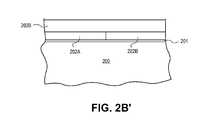
- FIG. 2 B′illustrates a cross-sectional view of an alternative stage in the fabrication of a back-contact solar cell corresponding to an operation of the flowchart of FIG. 1 , in accordance with an embodiment of the present invention.
- FIG. 2Cillustrates a cross-sectional view of a stage in the fabrication of a back-contact solar cell corresponding to an operation of the flowchart of FIG. 1 , in accordance with an embodiment of the present invention.
- FIG. 2Dillustrates a cross-sectional view of a stage in the fabrication of a back-contact solar cell corresponding to an operation of the flowchart of FIG. 1 , in accordance with an embodiment of the present invention.
- FIG. 3Aillustrates a cross-sectional view of a back-contact solar cell, in accordance with an embodiment of the present invention.
- FIG. 3Billustrates a cross-sectional view of a back-contact solar cell, in accordance with another embodiment of the present invention.
- FIG. 4illustrates a flowchart representing operations in a method of fabricating a back-contact solar cell, in accordance with an embodiment of the present invention.
- a methodincludes forming a poly-crystalline material layer above a single-crystalline substrate.
- a dielectric material stackis formed above the poly-crystalline material layer.
- a plurality of contacts holesis formed in the dielectric material stack by laser ablation, each of the contact holes exposing a portion of the poly-crystalline material layer.
- Conductive contactsare formed in the plurality of contact holes.
- a methodincludes forming a poly-crystalline material layer above a single-crystalline substrate.
- a dielectric material stackis formed above the poly-crystalline material layer.
- a recast poly signatureis formed in the poly-crystalline material layer.
- a plurality of conductive contactsis formed in the dielectric material stack and coupled directly to a portion of the poly-crystalline material layer, one of the conductive contacts in alignment with the recast poly signature. It is to be understood that embodiments of the present invention need not be limited to the formation of back-side contacts, but could be used to form front-side contacts instead or as well.
- a back-contact solar cellincludes a poly-crystalline material layer disposed above a single-crystalline substrate.
- a dielectric material stackis disposed above the poly-crystalline material layer.
- a plurality of conductive contactsis disposed in the dielectric material stack and coupled directly to a portion of the poly-crystalline material layer.
- a recast poly signatureis disposed in the poly-crystalline material layer and in alignment with one of the plurality of conductive contacts.
- contact formationis simplified and an associated cost of manufacture is reduced through reduction of consumables used, reduction of capital expenditure, and reduction of complexity.
- contact formation for a solar cellincludes contact formation in a dielectric layer by a direct-fire laser approach. Such an approach may otherwise be detrimental for single-crystal substrate based solar cells.
- a poly-crystalline layeris included above a single-crystal substrate based solar cell. In that embodiment, any damage or melt is received and accommodated by the poly-crystalline layer instead of by the single-crystal substrate.
- by using a poly-crystalline layer to receive a process of direct-fired contact formationthe formation of recombination sites in the single-crystal substrate is reduced or even essentially eliminated.
- such laser-induced damageis minimized or essentially eliminated with use of highly advanced lasers with ultra short pulse lengths (e.g., in the femto second range) and short wavelength light (UV).
- ultra short pulse lengthse.g., in the femto second range
- UVshort wavelength light
- standard cell architecturesmay still exhibit electrical degradation with such laser configurations.
- commercially available and reliably-tested lasersare applied to semi-conductors without causing additional emitter recombination sites.
- recombination in a solar cellis insensitive to typical optical and thermal damages induced by a laser since any damage remains within a poly-crystalline material layer instead on an underlying single-crystalline substrate.
- a contact resistance of a solar cell surfaceremains low after contact formation by laser.
- formation of a dielectric or passivation layer in combination with a poly-crystalline material layeris tuned in a way to accommodate commercially available lasers which confine any laser damage to the poly-crystalline material layer or to the dielectric or passivation layer.
- a pico-second laseris used and the thermal penetration depth in silicon is limited to a submicron level.
- an optical penetration depth in silicon during a laser-induced contact formation processis confined to a sub-micron level by using a laser wavelength less than approximately 1064 nanometers.
- an absorbing layersuch as a silicon nitride layer with the composition SixNy
- total thermal and optical damageis confined within a poly-crystalline material layer so that high-efficiencies are achieved in a solar cell without the need for post-laser etching processes, or selective emitter formation.
- a thin, e.g. less than approximately 15 nanometers, thermal oxide layeris grown to help mitigate thermal damage and promote ablation quality, optimizing a laser absorption process.
- an appropriately tuned poly/oxide/nitride stackis used to accommodate longer pulse length (e.g., nano-second), or higher wavelength lasers (e.g., 1064 nanometers).
- FIG. 1illustrates a flowchart 100 representing operations in a method of fabricating a back-contact solar cell, in accordance with an embodiment of the present invention.
- FIGS. 2A-2Dillustrate cross-sectional views of various stages in the fabrication of a back-contact solar cell corresponding to the operations of flowchart 100 , in accordance with an embodiment of the present invention.
- a method of fabricating a back-contact solar cellincludes forming a poly-crystalline material layer 202 above a single-crystalline substrate 200 .
- forming poly-crystalline material layer 202 above single-crystalline substrate 200includes forming a layer of poly-crystalline silicon above a single-crystalline silicon substrate.
- poly-crystalline material layer 202is formed to a thickness of approximately 200 nanometers.
- forming the layer of poly-crystalline silicon above the single-crystalline silicon substrateincludes forming the layer of poly-crystalline silicon directly on a dielectric film 201 , dielectric film 201 formed directly on single-crystalline silicon substrate 200 , and forming both N-type and P-type doped regions 202 A and 202 B, respectively, in the layer of poly-crystalline silicon, as depicted in FIG. 2A .
- the dielectric film 201is a material such as, but not limited to, silicon dioxide (SiO 2 ), phosphosilicate glass (PSG), or borosilicate glass (BSG) having a thickness approximately in the range of to 15 nanometers.
- dielectric film 201is composed of silicon dioxide and has a thickness approximately in the range of 1-2 nanometers.
- dielectric film 201is a tunnel oxide barrier layer film.
- a non-poly-crystalline absorbing materialis formed instead such as, but not limited to an amorphous layer, a polymer layer, or a multi-crystalline layer.
- a multi-crystalline substrateis used in its place.
- a trench or gapis present between the P and N diffused regions, e.g., in the case of one embodiment of a back-contact design.
- the method of fabricating a back-contact solar cellalso includes forming a dielectric material stack 204 above poly-crystalline material layer 202 .
- forming dielectric material stack 204 above poly-crystalline material layer 202includes forming a silicon dioxide layer 203 A directly on poly-crystalline material layer 202 , and forming a silicon nitride layer 203 B directly on silicon dioxide layer 203 A.
- forming silicon dioxide layer 203 Aincludes forming to a thickness sufficiently low to not reflect back laser energy during a laser ablation process.
- forming silicon dioxide layer 203 Aincludes forming to a thickness sufficiently high to act as an ablation stop layer during a laser ablation process. In one embodiment, forming silicon dioxide layer 203 A includes forming the layer to have a thickness approximately in the range of 1-50 nanometers. In a specific embodiment, forming silicon dioxide layer 203 A includes forming the layer to have a thickness approximately in the range of 5-15 nanometers. However, in another embodiment, there is no layer 203 A in the dielectric stack and only a silicon nitride layer 203 B is included, as depicted in FIG. 2 B′.
- the method of fabricating a back-contact solar cellalso includes forming, by laser ablation 206 , a plurality of contacts holes 208 in dielectric material stack 204 , each of the contact holes 208 exposing a portion of poly-crystalline material layer 202 .
- forming the plurality of contact holes 208is performed without the use of a patterned mask.
- forming the plurality of contact holes 208includes ablating with a laser having a wavelength approximately at, or less than, 1064 nanometers.
- the method of fabricating a back-contact solar cellalso includes forming conductive contacts 210 in the plurality of contact holes 208 .
- FIG. 3Aillustrates a cross-sectional view of a back-contact solar cell, in accordance with an embodiment of the present invention.
- a back-contact solar cell 300includes a poly-crystalline material layer 302 A+ 302 B disposed above a single-crystalline substrate 300 .
- a dielectric material stack 304is disposed above poly-crystalline material layer 302 A+ 302 B.
- a plurality of conductive contacts 310is disposed in dielectric material stack 304 and coupled directly to a portion of poly-crystalline material layer 302 A+ 302 B.
- a recast poly signature 320is disposed in poly-crystalline material layer 302 A+ 302 B and is in alignment with one of the plurality of conductive contacts 310 .
- poly-crystalline material layer 302 A+ 302 Bis a layer of poly-crystalline silicon
- single-crystalline substrate 300is a single-crystalline silicon substrate.
- the layer of poly-crystalline siliconis disposed directly on a dielectric film 301
- dielectric film 301is disposed directly on single-crystalline silicon substrate 300 , as depicted in FIG. 3A .
- the layer of poly-crystalline siliconincludes both N-type and P-type doped regions, 302 A+ 302 B, as is also depicted in FIG. 3A .
- dielectric material stack 304includes a silicon dioxide layer 303 A disposed directly on poly-crystalline material layer 302 A+ 302 B, and a silicon nitride layer 303 B disposed directly on silicon dioxide layer 303 A, as depicted in FIG. 3A .
- silicon dioxide layer 303 Ahas a thickness approximately in the range of 5-15 nanometers.
- each of the plurality of conductive contacts 310is round in shape.
- a non-poly-crystalline absorbing materialis formed instead such as, but not limited to an amorphous layer, a polymer layer, or a multi-crystalline layer.
- a multi-crystalline substrateis used in its place.
- a trench or gapis present between the P and N diffused regions, e.g., in the case of one embodiment of a back-contact design.
- a single dielectric material 303 B with a thickness approximately in the range of 5-15 nanometersis used, and layer 303 A is excluded.
- a back-contact solar cell having a recast poly signaturemay be formed when contact holes in the back-contact solar cell are formed by a laser ablation process.
- FIG. 4illustrates a flowchart 400 representing operations in a method of fabricating a back-contact solar cell, in accordance with an embodiment of the present invention.
- a method of fabricating a back-contact solar cellincludes forming a poly-crystalline material layer above a single-crystalline substrate.
- forming the poly-crystalline material layer above the single-crystalline substrateincludes forming a layer of poly-crystalline silicon above a single-crystalline silicon substrate.
- forming the layer of poly-crystalline silicon above the single-crystalline silicon substrateincludes forming the layer of poly-crystalline silicon directly on a dielectric film, the dielectric film formed directly on the single-crystalline silicon substrate, and forming both N-type and P-type doped regions in the layer of poly-crystalline silicon.
- a non-poly-crystalline absorbing materialis formed instead such as, but not limited to an amorphous layer, a polymer layer, or a multi-crystalline layer.
- a multi-crystalline substrateis used in its place.
- a trench or gapis present between the P and N diffused regions, e.g., in the case of one embodiment of a back-contact design.
- the method of fabricating a back-contact solar cellalso includes forming a dielectric material stack above the poly-crystalline material layer.
- forming the dielectric material stack above the poly-crystalline material layerincludes forming a silicon dioxide layer directly on the poly-crystalline material layer, and forming a silicon nitride layer directly on the silicon dioxide layer.
- forming the silicon dioxide layerincludes forming the layer to have a thickness approximately in the range of 1-50 nanometers. In a specific embodiment, forming the silicon dioxide layer includes forming the layer to have a thickness approximately in the range of 5-15 nanometers.
- the method of fabricating a back-contact solar cellalso includes forming a recast poly signature in the poly-crystalline material layer.
- each of the plurality of conductive contactsis round in shape.
- the method of fabricating a back-contact solar cellalso includes forming a plurality of conductive contacts in the dielectric material stack and coupled directly to a portion of the poly-crystalline material layer, one of the conductive contacts in alignment with the recast poly signature.
- forming the recast poly signatureincludes ablating with a laser having a wavelength approximately at, or less than, 1064 nanometers.
- poly-crystalline layerwhen referring to a polycrystalline silicon layer, is intended to also cover material that can be described as amorphous- or ⁇ -silicon. It is also to be understood that, instead of or in addition to forming N-type and P-type doped regions in the poly-crystalline layer, such regions can instead be formed directly in a single crystalline substrate. It is also to be understood that a variety of laser pulse periodicities may be used for ablation. However, in an embodiment, laser ablation is performed with laser pulse lengths in the pico- to nano-second range.
- a method of fabricating a back-contact solar cellincludes forming a poly-crystalline material layer above a single-crystalline substrate.
- a dielectric material stackis formed above the poly-crystalline material layer.
- a plurality of contacts holesis formed in the dielectric material stack by laser ablation, each of the contact holes exposing a portion of the poly-crystalline material layer.
- Conductive contactsare formed in the plurality of contact holes.
- forming the plurality of contact holesis performed without the use of a patterned mask.
- forming the plurality of contact holesincludes ablating with a laser having a wavelength approximately at, or less than, 1064 nanometers.
- forming the poly-crystalline material layer above the single-crystalline substrateincludes forming a layer of poly-crystalline silicon above a single-crystalline silicon substrate.
Landscapes
- Photovoltaic Devices (AREA)
- Life Sciences & Earth Sciences (AREA)
- Engineering & Computer Science (AREA)
- Sustainable Development (AREA)
- Sustainable Energy (AREA)
Abstract
Description
Claims (13)
Priority Applications (17)
| Application Number | Priority Date | Filing Date | Title |
|---|---|---|---|
| US12/895,437US8324015B2 (en) | 2009-12-01 | 2010-09-30 | Solar cell contact formation using laser ablation |
| EP10834898.8AEP2507844B1 (en) | 2009-12-01 | 2010-10-01 | Solar cell contact formation using laser ablation |
| PH1/2012/500956APH12012500956A1 (en) | 2009-12-01 | 2010-10-01 | Solar cell contact formation using laser ablation |
| JP2012542005AJP5726892B2 (en) | 2009-12-01 | 2010-10-01 | Formation of solar cell contacts using laser ablation |
| CN201080054693.2ACN102640300B (en) | 2009-12-01 | 2010-10-01 | Contact formation of solar cells using laser ablation |
| CN201710165852.XACN107134498B (en) | 2009-12-01 | 2010-10-01 | It is formed using the contact of the solar battery of laser ablation |
| EP20165212.0AEP3723141B1 (en) | 2009-12-01 | 2010-10-01 | Solar cell contact formation using laser ablation |
| MYPI2012002257AMY155779A (en) | 2009-12-01 | 2010-10-01 | Solar cell contact formation using laser ablation |
| EP23210934.8AEP4300598B1 (en) | 2009-12-01 | 2010-10-01 | Solar cell contact formation using laser ablation |
| PCT/US2010/051178WO2011068590A2 (en) | 2009-12-01 | 2010-10-01 | Solar cell contact formation using laser ablation |
| US13/669,147US8785236B2 (en) | 2009-12-01 | 2012-11-05 | Solar cell contact formation using laser ablation |
| US14/334,401US9087939B2 (en) | 2009-12-01 | 2014-07-17 | Solar cell contact formation using laser ablation |
| JP2015075493AJP6089058B2 (en) | 2009-12-01 | 2015-04-01 | Manufacturing method of solar cell |
| US14/793,356US10211349B2 (en) | 2009-12-01 | 2015-07-07 | Solar cell contact formation using laser ablation |
| JP2017019684AJP6648358B2 (en) | 2009-12-01 | 2017-02-06 | Solar cell |
| US16/276,381US11152518B2 (en) | 2009-12-01 | 2019-02-14 | Solar cell having a plurality of conductive contacts |
| US17/498,979US12191404B2 (en) | 2009-12-01 | 2021-10-12 | Solar cell having conductive contacts in alignment with recast signatures |
Applications Claiming Priority (2)
| Application Number | Priority Date | Filing Date | Title |
|---|---|---|---|
| US26565209P | 2009-12-01 | 2009-12-01 | |
| US12/895,437US8324015B2 (en) | 2009-12-01 | 2010-09-30 | Solar cell contact formation using laser ablation |
Related Child Applications (2)
| Application Number | Title | Priority Date | Filing Date |
|---|---|---|---|
| US13/668,147ContinuationUS9336618B1 (en) | 2012-11-02 | 2012-11-02 | Stochastic chunk-based map generation |
| US13/669,147ContinuationUS8785236B2 (en) | 2009-12-01 | 2012-11-05 | Solar cell contact formation using laser ablation |
Publications (2)
| Publication Number | Publication Date |
|---|---|
| US20110126898A1 US20110126898A1 (en) | 2011-06-02 |
| US8324015B2true US8324015B2 (en) | 2012-12-04 |
Family
ID=44067930
Family Applications (6)
| Application Number | Title | Priority Date | Filing Date |
|---|---|---|---|
| US12/895,437Active2031-06-29US8324015B2 (en) | 2009-12-01 | 2010-09-30 | Solar cell contact formation using laser ablation |
| US13/669,147ActiveUS8785236B2 (en) | 2009-12-01 | 2012-11-05 | Solar cell contact formation using laser ablation |
| US14/334,401ActiveUS9087939B2 (en) | 2009-12-01 | 2014-07-17 | Solar cell contact formation using laser ablation |
| US14/793,356Active2031-08-06US10211349B2 (en) | 2009-12-01 | 2015-07-07 | Solar cell contact formation using laser ablation |
| US16/276,381Active2031-04-21US11152518B2 (en) | 2009-12-01 | 2019-02-14 | Solar cell having a plurality of conductive contacts |
| US17/498,979Active2032-03-21US12191404B2 (en) | 2009-12-01 | 2021-10-12 | Solar cell having conductive contacts in alignment with recast signatures |
Family Applications After (5)
| Application Number | Title | Priority Date | Filing Date |
|---|---|---|---|
| US13/669,147ActiveUS8785236B2 (en) | 2009-12-01 | 2012-11-05 | Solar cell contact formation using laser ablation |
| US14/334,401ActiveUS9087939B2 (en) | 2009-12-01 | 2014-07-17 | Solar cell contact formation using laser ablation |
| US14/793,356Active2031-08-06US10211349B2 (en) | 2009-12-01 | 2015-07-07 | Solar cell contact formation using laser ablation |
| US16/276,381Active2031-04-21US11152518B2 (en) | 2009-12-01 | 2019-02-14 | Solar cell having a plurality of conductive contacts |
| US17/498,979Active2032-03-21US12191404B2 (en) | 2009-12-01 | 2021-10-12 | Solar cell having conductive contacts in alignment with recast signatures |
Country Status (7)
| Country | Link |
|---|---|
| US (6) | US8324015B2 (en) |
| EP (3) | EP2507844B1 (en) |
| JP (3) | JP5726892B2 (en) |
| CN (2) | CN107134498B (en) |
| MY (1) | MY155779A (en) |
| PH (1) | PH12012500956A1 (en) |
| WO (1) | WO2011068590A2 (en) |
Cited By (14)
| Publication number | Priority date | Publication date | Assignee | Title |
|---|---|---|---|---|
| US20120171807A1 (en)* | 2010-12-29 | 2012-07-05 | Berger Alexander J | Method and apparatus for masking substrates for deposition |
| US20130065357A1 (en)* | 2009-12-01 | 2013-03-14 | Sunpower Corporation | Solar cell contact formation using laser ablation |
| US20170005206A1 (en)* | 2007-10-06 | 2017-01-05 | Solexel, Inc. | Patterning of silicon oxide layers using pulsed laser ablation |
| USD822890S1 (en) | 2016-09-07 | 2018-07-10 | Felxtronics Ap, Llc | Lighting apparatus |
| USD832495S1 (en) | 2017-08-18 | 2018-10-30 | Flex Ltd. | Lighting module locking mechanism |
| USD832494S1 (en) | 2017-08-09 | 2018-10-30 | Flex Ltd. | Lighting module heatsink |
| USD833061S1 (en) | 2017-08-09 | 2018-11-06 | Flex Ltd. | Lighting module locking endcap |
| USD846793S1 (en) | 2017-08-09 | 2019-04-23 | Flex Ltd. | Lighting module locking mechanism |
| USD862777S1 (en) | 2017-08-09 | 2019-10-08 | Flex Ltd. | Lighting module wide distribution lens |
| USD862778S1 (en) | 2017-08-22 | 2019-10-08 | Flex Ltd | Lighting module lens |
| USD872319S1 (en) | 2017-08-09 | 2020-01-07 | Flex Ltd. | Lighting module LED light board |
| USD877964S1 (en) | 2017-08-09 | 2020-03-10 | Flex Ltd. | Lighting module |
| USD888323S1 (en) | 2017-09-07 | 2020-06-23 | Flex Ltd | Lighting module wire guard |
| US10775030B2 (en) | 2017-05-05 | 2020-09-15 | Flex Ltd. | Light fixture device including rotatable light modules |
Families Citing this family (25)
| Publication number | Priority date | Publication date | Assignee | Title |
|---|---|---|---|---|
| US8242354B2 (en)* | 2008-12-04 | 2012-08-14 | Sunpower Corporation | Backside contact solar cell with formed polysilicon doped regions |
| US8658458B2 (en)* | 2011-06-15 | 2014-02-25 | Varian Semiconductor Equipment Associates, Inc. | Patterned doping for polysilicon emitter solar cells |
| US8692111B2 (en)* | 2011-08-23 | 2014-04-08 | Sunpower Corporation | High throughput laser ablation processes and structures for forming contact holes in solar cells |
| EP2579317A1 (en)* | 2011-10-07 | 2013-04-10 | Total SA | Method of manufacturing a solar cell with local back contacts |
| CN103890978A (en)* | 2011-10-28 | 2014-06-25 | 应用材料公司 | Back Contact Via Formation Process for Solar Cell Manufacturing |
| US20130199606A1 (en)* | 2012-02-06 | 2013-08-08 | Applied Materials, Inc. | Methods of manufacturing back surface field and metallized contacts on a solar cell device |
| DE102012205966A1 (en)* | 2012-04-12 | 2013-10-17 | Robert Bosch Gmbh | Method for producing a thin-film solar module |
| US9847438B2 (en)* | 2013-03-15 | 2017-12-19 | Sunpower Corporation | Reduced contact resistance and improved lifetime of solar cells |
| EP4092764A1 (en) | 2013-04-03 | 2022-11-23 | Lg Electronics Inc. | Solar cell |
| KR101613843B1 (en)* | 2013-04-23 | 2016-04-20 | 엘지전자 주식회사 | Solar cell and method for manufacturing the same |
| WO2014179368A1 (en)* | 2013-04-29 | 2014-11-06 | Solexel, Inc. | Damage free laser patterning of transparent layers for forming doped regions on a solar cell substrate |
| KR102045001B1 (en)* | 2013-06-05 | 2019-12-02 | 엘지전자 주식회사 | Solar cell and method for manufacturing the same |
| KR101622089B1 (en)* | 2013-07-05 | 2016-05-18 | 엘지전자 주식회사 | Solar cell and method for manufacturing the same |
| KR101620431B1 (en)* | 2014-01-29 | 2016-05-12 | 엘지전자 주식회사 | Solar cell and method for manufacturing the same |
| KR101569415B1 (en) | 2014-06-09 | 2015-11-16 | 엘지전자 주식회사 | Method for manufacturing solar cell |
| KR102219804B1 (en) | 2014-11-04 | 2021-02-24 | 엘지전자 주식회사 | Solar cell and the manufacturing mathod thereof |
| US9722104B2 (en) | 2014-11-28 | 2017-08-01 | Lg Electronics Inc. | Solar cell and method for manufacturing the same |
| US10535790B2 (en)* | 2015-06-25 | 2020-01-14 | Sunpower Corporation | One-dimensional metallization for solar cells |
| KR102272433B1 (en) | 2015-06-30 | 2021-07-05 | 엘지전자 주식회사 | Solar cell and method of manufacturing the same |
| KR102600379B1 (en) | 2015-12-21 | 2023-11-10 | 상라오 징코 솔라 테크놀러지 디벨롭먼트 컴퍼니, 리미티드 | Solar cell and method for fabricating therefor |
| KR102526398B1 (en)* | 2016-01-12 | 2023-04-27 | 상라오 징코 솔라 테크놀러지 디벨롭먼트 컴퍼니, 리미티드 | Solar cell and method for manufacturing the same |
| JP2017143267A (en)* | 2016-02-12 | 2017-08-17 | エルジー エレクトロニクス インコーポレイティド | Solar cell and manufacturing method thereof |
| KR102350960B1 (en)* | 2019-04-25 | 2022-01-14 | 엘지전자 주식회사 | methods for fabricating a solar cell |
| US12329704B2 (en) | 2021-08-23 | 2025-06-17 | Medline Industries, Lp | Absorbent repositioning pad and method |
| CN117059681B (en) | 2023-10-09 | 2024-03-29 | 晶科能源(海宁)有限公司 | Solar cells and manufacturing methods thereof, photovoltaic modules |
Citations (18)
| Publication number | Priority date | Publication date | Assignee | Title |
|---|---|---|---|---|
| US4626613A (en) | 1983-12-23 | 1986-12-02 | Unisearch Limited | Laser grooved solar cell |
| US5011565A (en) | 1989-12-06 | 1991-04-30 | Mobil Solar Energy Corporation | Dotted contact solar cell and method of making same |
| US5183780A (en) | 1990-02-22 | 1993-02-02 | Sanyo Electric Co., Ltd. | Method of fabricating semiconductor device |
| US5258077A (en) | 1991-09-13 | 1993-11-02 | Solec International, Inc. | High efficiency silicon solar cells and method of fabrication |
| US5456763A (en) | 1994-03-29 | 1995-10-10 | The Regents Of The University Of California | Solar cells utilizing pulsed-energy crystallized microcrystalline/polycrystalline silicon |
| US5738731A (en)* | 1993-11-19 | 1998-04-14 | Mega Chips Corporation | Photovoltaic device |
| US6172297B1 (en) | 1997-09-23 | 2001-01-09 | Institut Fur Solarenergieforschung Gmbh | Solar cell and method for fabrication of a solar cell |
| US6982218B2 (en) | 2000-09-19 | 2006-01-03 | Fraunhofer-Gesellschaft Zur Forderung Der Angewandten Forschung E.V. | Method of producing a semiconductor-metal contact through a dielectric layer |
| US20070137692A1 (en) | 2005-12-16 | 2007-06-21 | Bp Corporation North America Inc. | Back-Contact Photovoltaic Cells |
| US20080035198A1 (en) | 2004-10-14 | 2008-02-14 | Institut Fur Solarenergieforschung Gmbh | Method for the Contact Separation of Electrically-Conducting Layers on the Back Contacts of Solar Cells and Corresponding Solar Cells |
| JP2008283023A (en) | 2007-05-11 | 2008-11-20 | Mitsubishi Heavy Ind Ltd | Production process of photoelectric conversion device |
| JP2009071221A (en) | 2007-09-18 | 2009-04-02 | Mitsubishi Heavy Ind Ltd | Photoelectric conversion device and manufacturing method of photoelectric conversion device |
| US20090107545A1 (en) | 2006-10-09 | 2009-04-30 | Soltaix, Inc. | Template for pyramidal three-dimensional thin-film solar cell manufacturing and methods of use |
| US20090188553A1 (en)* | 2008-01-25 | 2009-07-30 | Emat Technology, Llc | Methods of fabricating solar-cell structures and resulting solar-cell structures |
| US20090239331A1 (en)* | 2008-03-24 | 2009-09-24 | Palo Alto Research Center Incorporated | Methods for forming multiple-layer electrode structures for silicon photovoltaic cells |
| US20100304522A1 (en) | 2009-05-05 | 2010-12-02 | Solexel, Inc. | Ion implantation fabrication process for thin-film crystalline silicon solar cells |
| US20120028399A1 (en) | 2007-10-06 | 2012-02-02 | Solexel, Inc. | Laser processing for high-efficiency thin crystalline silicon solar cell fabrication |
| US8129822B2 (en) | 2006-10-09 | 2012-03-06 | Solexel, Inc. | Template for three-dimensional thin-film solar cell manufacturing and methods of use |
Family Cites Families (39)
| Publication number | Priority date | Publication date | Assignee | Title |
|---|---|---|---|---|
| US4900695A (en)* | 1986-12-17 | 1990-02-13 | Hitachi, Ltd. | Semiconductor integrated circuit device and process for producing the same |
| JP2706113B2 (en) | 1988-11-25 | 1998-01-28 | 工業技術院長 | Photoelectric conversion element |
| US5053083A (en)* | 1989-05-08 | 1991-10-01 | The Board Of Trustees Of The Leland Stanford Junior University | Bilevel contact solar cells |
| JP3193287B2 (en)* | 1996-02-28 | 2001-07-30 | シャープ株式会社 | Solar cell |
| JPH10229211A (en)* | 1997-02-18 | 1998-08-25 | Hitachi Ltd | Photoelectric conversion device and method of manufacturing the same |
| US6126565A (en) | 1999-03-31 | 2000-10-03 | Dana Corporation | Method for controlling flow of lubrication in axle assembly and axle assembly with selectively adjustable drain-back spacer |
| JP2003298078A (en) | 2002-03-29 | 2003-10-17 | Ebara Corp | Photovoltaic element |
| US7388147B2 (en)* | 2003-04-10 | 2008-06-17 | Sunpower Corporation | Metal contact structure for solar cell and method of manufacture |
| US20050172996A1 (en)* | 2004-02-05 | 2005-08-11 | Advent Solar, Inc. | Contact fabrication of emitter wrap-through back contact silicon solar cells |
| WO2005093900A1 (en)* | 2004-03-26 | 2005-10-06 | Semiconductor Energy Laboratory Co., Ltd. | Semiconductor device |
| US20060130891A1 (en)* | 2004-10-29 | 2006-06-22 | Carlson David E | Back-contact photovoltaic cells |
| FR2880989B1 (en)* | 2005-01-20 | 2007-03-09 | Commissariat Energie Atomique | SEMICONDUCTOR DEVICE WITH HETEROJUNCTIONS AND INTERDIGITAL STRUCTURE |
| EP1763086A1 (en) | 2005-09-09 | 2007-03-14 | Interuniversitair Micro-Elektronica Centrum | Photovoltaic cell with thick silicon oxide and silicon nitride passivation and fabrication method |
| US7279362B2 (en)* | 2005-03-31 | 2007-10-09 | Intel Corporation | Semiconductor wafer coat layers and methods therefor |
| DE102005040871A1 (en)* | 2005-04-16 | 2006-10-19 | Institut Für Solarenergieforschung Gmbh | Back contacted solar cell and process for its production |
| US7468485B1 (en)* | 2005-08-11 | 2008-12-23 | Sunpower Corporation | Back side contact solar cell with doped polysilicon regions |
| JP2009152222A (en)* | 2006-10-27 | 2009-07-09 | Kyocera Corp | Method for manufacturing solar cell element |
| US7705237B2 (en)* | 2006-11-27 | 2010-04-27 | Sunpower Corporation | Solar cell having silicon nano-particle emitter |
| US8853527B2 (en)* | 2007-02-16 | 2014-10-07 | Nanogram Corporation | Solar cell structures, photovoltaic panels and corresponding processes |
| EP2135292A2 (en)* | 2007-03-16 | 2009-12-23 | BP Corporation North America Inc. | Solar cells |
| KR101293162B1 (en)* | 2007-11-09 | 2013-08-12 | 선프림, 리미티드 | Low-cost solar cells and methods for their production |
| US8198528B2 (en)* | 2007-12-14 | 2012-06-12 | Sunpower Corporation | Anti-reflective coating with high optical absorption layer for backside contact solar cells |
| US7820540B2 (en)* | 2007-12-21 | 2010-10-26 | Palo Alto Research Center Incorporated | Metallization contact structures and methods for forming multiple-layer electrode structures for silicon solar cells |
| WO2009094575A2 (en)* | 2008-01-24 | 2009-07-30 | Applied Materials, Inc. | Buried insulator isolation for solar cell contacts |
| KR100864062B1 (en)* | 2008-02-22 | 2008-10-16 | 한국철강 주식회사 | Solar Module Patterning Device |
| KR101155343B1 (en)* | 2008-02-25 | 2012-06-11 | 엘지전자 주식회사 | Fabrication method of back contact solar cell |
| US20090314341A1 (en)* | 2008-04-09 | 2009-12-24 | Borden Peter G | Simplified back contact for polysilicon emitter solar cells |
| EP2195853B1 (en)* | 2008-04-17 | 2015-12-16 | LG Electronics Inc. | Solar cell and method of manufacturing the same |
| US7851698B2 (en)* | 2008-06-12 | 2010-12-14 | Sunpower Corporation | Trench process and structure for backside contact solar cells with polysilicon doped regions |
| US20100071765A1 (en)* | 2008-09-19 | 2010-03-25 | Peter Cousins | Method for fabricating a solar cell using a direct-pattern pin-hole-free masking layer |
| US8242354B2 (en) | 2008-12-04 | 2012-08-14 | Sunpower Corporation | Backside contact solar cell with formed polysilicon doped regions |
| CN101447518A (en)* | 2008-12-31 | 2009-06-03 | 江苏艾德太阳能科技有限公司 | Ant-apex contact heterojunction solar battery and preparation method thereof |
| EP2422374A4 (en) | 2009-04-21 | 2016-09-14 | Tetrasun Inc | METHOD FOR FORMATION OF STRUCTURES IN A SOLAR CELL |
| WO2010123980A1 (en) | 2009-04-22 | 2010-10-28 | Tetrasun, Inc. | Localized metal contacts by localized laser assisted conversion of functional films in solar cells |
| US8324015B2 (en) | 2009-12-01 | 2012-12-04 | Sunpower Corporation | Solar cell contact formation using laser ablation |
| CN103890978A (en) | 2011-10-28 | 2014-06-25 | 应用材料公司 | Back Contact Via Formation Process for Solar Cell Manufacturing |
| DE102012205966A1 (en) | 2012-04-12 | 2013-10-17 | Robert Bosch Gmbh | Method for producing a thin-film solar module |
| US9847438B2 (en) | 2013-03-15 | 2017-12-19 | Sunpower Corporation | Reduced contact resistance and improved lifetime of solar cells |
| WO2014179368A1 (en) | 2013-04-29 | 2014-11-06 | Solexel, Inc. | Damage free laser patterning of transparent layers for forming doped regions on a solar cell substrate |
- 2010
- 2010-09-30USUS12/895,437patent/US8324015B2/enactiveActive
- 2010-10-01WOPCT/US2010/051178patent/WO2011068590A2/enactiveApplication Filing
- 2010-10-01MYMYPI2012002257Apatent/MY155779A/enunknown
- 2010-10-01PHPH1/2012/500956Apatent/PH12012500956A1/enunknown
- 2010-10-01CNCN201710165852.XApatent/CN107134498B/enactiveActive
- 2010-10-01EPEP10834898.8Apatent/EP2507844B1/enactiveActive
- 2010-10-01JPJP2012542005Apatent/JP5726892B2/enactiveActive
- 2010-10-01EPEP20165212.0Apatent/EP3723141B1/enactiveActive
- 2010-10-01EPEP23210934.8Apatent/EP4300598B1/enactiveActive
- 2010-10-01CNCN201080054693.2Apatent/CN102640300B/enactiveActive
- 2012
- 2012-11-05USUS13/669,147patent/US8785236B2/enactiveActive
- 2014
- 2014-07-17USUS14/334,401patent/US9087939B2/enactiveActive
- 2015
- 2015-04-01JPJP2015075493Apatent/JP6089058B2/enactiveActive
- 2015-07-07USUS14/793,356patent/US10211349B2/enactiveActive
- 2017
- 2017-02-06JPJP2017019684Apatent/JP6648358B2/enactiveActive
- 2019
- 2019-02-14USUS16/276,381patent/US11152518B2/enactiveActive
- 2021
- 2021-10-12USUS17/498,979patent/US12191404B2/enactiveActive
Patent Citations (18)
| Publication number | Priority date | Publication date | Assignee | Title |
|---|---|---|---|---|
| US4626613A (en) | 1983-12-23 | 1986-12-02 | Unisearch Limited | Laser grooved solar cell |
| US5011565A (en) | 1989-12-06 | 1991-04-30 | Mobil Solar Energy Corporation | Dotted contact solar cell and method of making same |
| US5183780A (en) | 1990-02-22 | 1993-02-02 | Sanyo Electric Co., Ltd. | Method of fabricating semiconductor device |
| US5258077A (en) | 1991-09-13 | 1993-11-02 | Solec International, Inc. | High efficiency silicon solar cells and method of fabrication |
| US5738731A (en)* | 1993-11-19 | 1998-04-14 | Mega Chips Corporation | Photovoltaic device |
| US5456763A (en) | 1994-03-29 | 1995-10-10 | The Regents Of The University Of California | Solar cells utilizing pulsed-energy crystallized microcrystalline/polycrystalline silicon |
| US6172297B1 (en) | 1997-09-23 | 2001-01-09 | Institut Fur Solarenergieforschung Gmbh | Solar cell and method for fabrication of a solar cell |
| US6982218B2 (en) | 2000-09-19 | 2006-01-03 | Fraunhofer-Gesellschaft Zur Forderung Der Angewandten Forschung E.V. | Method of producing a semiconductor-metal contact through a dielectric layer |
| US20080035198A1 (en) | 2004-10-14 | 2008-02-14 | Institut Fur Solarenergieforschung Gmbh | Method for the Contact Separation of Electrically-Conducting Layers on the Back Contacts of Solar Cells and Corresponding Solar Cells |
| US20070137692A1 (en) | 2005-12-16 | 2007-06-21 | Bp Corporation North America Inc. | Back-Contact Photovoltaic Cells |
| US20090107545A1 (en) | 2006-10-09 | 2009-04-30 | Soltaix, Inc. | Template for pyramidal three-dimensional thin-film solar cell manufacturing and methods of use |
| US8129822B2 (en) | 2006-10-09 | 2012-03-06 | Solexel, Inc. | Template for three-dimensional thin-film solar cell manufacturing and methods of use |
| JP2008283023A (en) | 2007-05-11 | 2008-11-20 | Mitsubishi Heavy Ind Ltd | Production process of photoelectric conversion device |
| JP2009071221A (en) | 2007-09-18 | 2009-04-02 | Mitsubishi Heavy Ind Ltd | Photoelectric conversion device and manufacturing method of photoelectric conversion device |
| US20120028399A1 (en) | 2007-10-06 | 2012-02-02 | Solexel, Inc. | Laser processing for high-efficiency thin crystalline silicon solar cell fabrication |
| US20090188553A1 (en)* | 2008-01-25 | 2009-07-30 | Emat Technology, Llc | Methods of fabricating solar-cell structures and resulting solar-cell structures |
| US20090239331A1 (en)* | 2008-03-24 | 2009-09-24 | Palo Alto Research Center Incorporated | Methods for forming multiple-layer electrode structures for silicon photovoltaic cells |
| US20100304522A1 (en) | 2009-05-05 | 2010-12-02 | Solexel, Inc. | Ion implantation fabrication process for thin-film crystalline silicon solar cells |
Non-Patent Citations (9)
| Title |
|---|
| Engelhart, et al., "Laser Ablation of SiO2 for Locally Contacted Si Solar Cells With Ultra-short Pulses," Prog. Photovolt. Res. Appl. 2007: 15:521-527. |
| Glunz, et al., "New Simplified Methods for Patterning the Rear Contact of RP-PERC High-Efficiency Solar Cells," IEEE, 2000, 168-171. |
| Hermann, et al., "Process Characterisation of Picosecond Laser Ablation of SiO2 and SiNx Layers on Planar and Textured Surfaces," Proceedings of the 23rd European Photovoltaic Solar Energy Conference, Sep. 2008, 5 pgs. |
| Hofmann, et al., "Industrial Type CZ Silicon Solar Cells With Screen-Printed Fine Line Front Contacts and Passivated Rear Contacted by Laser Firing," 23rd European Photovoltaic Solar Energy Conference and Exhibition, Sep. 1-5, 2008, 4 pgs. |
| International Search Report and Written Opinion from PCT/US2010/051178 mailed Jun. 8, 2011, 9 pgs. |
| Knorz, et al., "Laser Ablation of Antireflection Coatings for Plated Contacts Yielding Solar Cell Efficiencies Above 20%," 24th European PV Solar Energy Conference and Exhibition, Sep. 21-25, 2009, 4 pgs. |
| Preu, et al., "Laser Ablation-A New Low-Cost Approach for Passivated Rear Contact Formation in Crystalline Silicon Solar Cell Technology," 16th European Photovoltaic Solar Energy Conference, May 1-5, 2000, 4 pgs. |
| Schneiderlöchner, et al., "Laser-Fired Rear Contacts for Crystalline Silicon Solar Cells," Prog. Photovolt: Res. Appl. 2002; 10:29-34. |
| U.S. Appl. No. 61/349,120, filed May 27, 2010, entitled "Laser Processing for High-Efficiency Solar Cell Fabrication," 23 pgs. |
Cited By (29)
| Publication number | Priority date | Publication date | Assignee | Title |
|---|---|---|---|---|
| US20170005206A1 (en)* | 2007-10-06 | 2017-01-05 | Solexel, Inc. | Patterning of silicon oxide layers using pulsed laser ablation |
| US8785236B2 (en)* | 2009-12-01 | 2014-07-22 | Sunpower Corporation | Solar cell contact formation using laser ablation |
| US20140326308A1 (en)* | 2009-12-01 | 2014-11-06 | Sunpower Corporation | Solar cell contact formation using laser ablation |
| US9087939B2 (en)* | 2009-12-01 | 2015-07-21 | Sunpower Corporation | Solar cell contact formation using laser ablation |
| US20130065357A1 (en)* | 2009-12-01 | 2013-03-14 | Sunpower Corporation | Solar cell contact formation using laser ablation |
| US12191404B2 (en)* | 2009-12-01 | 2025-01-07 | Maxeon Solar Pte. Ltd. | Solar cell having conductive contacts in alignment with recast signatures |
| US20220029038A1 (en)* | 2009-12-01 | 2022-01-27 | Sunpower Corporation | Solar cell contact formation using laser ablation |
| US11152518B2 (en)* | 2009-12-01 | 2021-10-19 | Sunpower Corporation | Solar cell having a plurality of conductive contacts |
| US10211349B2 (en)* | 2009-12-01 | 2019-02-19 | Sunpower Corporation | Solar cell contact formation using laser ablation |
| US8677929B2 (en)* | 2010-12-29 | 2014-03-25 | Intevac, Inc. | Method and apparatus for masking solar cell substrates for deposition |
| US20120171807A1 (en)* | 2010-12-29 | 2012-07-05 | Berger Alexander J | Method and apparatus for masking substrates for deposition |
| USD822890S1 (en) | 2016-09-07 | 2018-07-10 | Felxtronics Ap, Llc | Lighting apparatus |
| US10775030B2 (en) | 2017-05-05 | 2020-09-15 | Flex Ltd. | Light fixture device including rotatable light modules |
| USD885615S1 (en) | 2017-08-09 | 2020-05-26 | Flex Ltd. | Lighting module LED light board |
| USD877964S1 (en) | 2017-08-09 | 2020-03-10 | Flex Ltd. | Lighting module |
| USD853627S1 (en) | 2017-08-09 | 2019-07-09 | Flex Ltd | Lighting module locking endcap |
| USD853625S1 (en) | 2017-08-09 | 2019-07-09 | Flex Ltd | Lighting module heatsink |
| USD862777S1 (en) | 2017-08-09 | 2019-10-08 | Flex Ltd. | Lighting module wide distribution lens |
| USD1010915S1 (en) | 2017-08-09 | 2024-01-09 | Linmore Labs Led, Inc. | Lighting module |
| USD872319S1 (en) | 2017-08-09 | 2020-01-07 | Flex Ltd. | Lighting module LED light board |
| USD832494S1 (en) | 2017-08-09 | 2018-10-30 | Flex Ltd. | Lighting module heatsink |
| USD853629S1 (en) | 2017-08-09 | 2019-07-09 | Flex Ltd | Lighting module locking mechanism |
| USD833061S1 (en) | 2017-08-09 | 2018-11-06 | Flex Ltd. | Lighting module locking endcap |
| USD846793S1 (en) | 2017-08-09 | 2019-04-23 | Flex Ltd. | Lighting module locking mechanism |
| USD905325S1 (en) | 2017-08-09 | 2020-12-15 | Flex Ltd | Lighting module |
| USD853628S1 (en) | 2017-08-18 | 2019-07-09 | Flex Ltd. | Lighting module locking mechanism |
| USD832495S1 (en) | 2017-08-18 | 2018-10-30 | Flex Ltd. | Lighting module locking mechanism |
| USD862778S1 (en) | 2017-08-22 | 2019-10-08 | Flex Ltd | Lighting module lens |
| USD888323S1 (en) | 2017-09-07 | 2020-06-23 | Flex Ltd | Lighting module wire guard |
Also Published As
| Publication number | Publication date |
|---|---|
| JP2017076826A (en) | 2017-04-20 |
| EP4300598A3 (en) | 2024-03-27 |
| CN102640300B (en) | 2017-04-12 |
| EP4300598B1 (en) | 2025-04-09 |
| MY155779A (en) | 2015-11-30 |
| JP5726892B2 (en) | 2015-06-03 |
| JP6648358B2 (en) | 2020-02-14 |
| EP3723141C0 (en) | 2023-11-22 |
| PH12012500956A1 (en) | 2013-01-07 |
| US12191404B2 (en) | 2025-01-07 |
| US20130065357A1 (en) | 2013-03-14 |
| WO2011068590A3 (en) | 2011-08-04 |
| US9087939B2 (en) | 2015-07-21 |
| JP2013512582A (en) | 2013-04-11 |
| US20110126898A1 (en) | 2011-06-02 |
| CN107134498A (en) | 2017-09-05 |
| EP4300598A2 (en) | 2024-01-03 |
| US20190245099A1 (en) | 2019-08-08 |
| EP2507844A2 (en) | 2012-10-10 |
| US20220029038A1 (en) | 2022-01-27 |
| US20140326308A1 (en) | 2014-11-06 |
| CN107134498B (en) | 2019-06-28 |
| US20150311357A1 (en) | 2015-10-29 |
| JP6089058B2 (en) | 2017-03-01 |
| US10211349B2 (en) | 2019-02-19 |
| US20140134787A9 (en) | 2014-05-15 |
| EP2507844B1 (en) | 2020-03-25 |
| US11152518B2 (en) | 2021-10-19 |
| CN102640300A (en) | 2012-08-15 |
| US8785236B2 (en) | 2014-07-22 |
| EP3723141A1 (en) | 2020-10-14 |
| EP3723141B1 (en) | 2023-11-22 |
| EP2507844A4 (en) | 2013-12-25 |
| WO2011068590A2 (en) | 2011-06-09 |
| JP2015146446A (en) | 2015-08-13 |
Similar Documents
| Publication | Publication Date | Title |
|---|---|---|
| US12191404B2 (en) | Solar cell having conductive contacts in alignment with recast signatures | |
| US9768343B2 (en) | Damage free laser patterning of transparent layers for forming doped regions on a solar cell substrate | |
| CN103370801B (en) | Method and structure for making solar cells | |
| US8637340B2 (en) | Patterning of silicon oxide layers using pulsed laser ablation | |
| US9508886B2 (en) | Method for making a crystalline silicon solar cell substrate utilizing flat top laser beam | |
| US9455362B2 (en) | Laser irradiation aluminum doping for monocrystalline silicon substrates | |
| US20120225515A1 (en) | Laser doping techniques for high-efficiency crystalline semiconductor solar cells | |
| US20130164883A1 (en) | Laser annealing applications in high-efficiency solar cells | |
| US20100024864A1 (en) | Solar cell, method of manufacturing the same, and solar cell module | |
| US20110014772A1 (en) | Aligning method of patterned electrode in a selective emitter structure | |
| EP2819181A1 (en) | Laser annealing applications in high-efficiency solar cells | |
| Harley et al. | Solar cell having a plurality of conductive contacts |
Legal Events
| Date | Code | Title | Description |
|---|---|---|---|
| AS | Assignment | Owner name:SUNPOWER CORPORATION, CALIFORNIA Free format text:ASSIGNMENT OF ASSIGNORS INTEREST;ASSIGNORS:HARLEY, GABRIEL;SMITH, DAVID;COUSINS, PETER;REEL/FRAME:025475/0196 Effective date:20101130 | |
| AS | Assignment | Owner name:UNITED STATE DEPARTMENT OF ENERGY, DISTRICT OF COL Free format text:CONFIRMATORY LICENSE;ASSIGNOR:SUNPOWER CORPORATION;REEL/FRAME:028560/0749 Effective date:20120312 | |
| STCF | Information on status: patent grant | Free format text:PATENTED CASE | |
| FPAY | Fee payment | Year of fee payment:4 | |
| MAFP | Maintenance fee payment | Free format text:PAYMENT OF MAINTENANCE FEE, 8TH YEAR, LARGE ENTITY (ORIGINAL EVENT CODE: M1552); ENTITY STATUS OF PATENT OWNER: LARGE ENTITY Year of fee payment:8 | |
| AS | Assignment | Owner name:MAXEON SOLAR PTE. LTD., SINGAPORE Free format text:ASSIGNMENT OF ASSIGNORS INTEREST;ASSIGNOR:SUNPOWER CORPORATION;REEL/FRAME:062490/0742 Effective date:20221214 | |
| MAFP | Maintenance fee payment | Free format text:PAYMENT OF MAINTENANCE FEE, 12TH YEAR, LARGE ENTITY (ORIGINAL EVENT CODE: M1553); ENTITY STATUS OF PATENT OWNER: LARGE ENTITY Year of fee payment:12 | |
| AS | Assignment | Owner name:DB TRUSTEES (HONG KONG) LIMITED, HONG KONG Free format text:SECURITY INTEREST;ASSIGNOR:MAXEON SOLAR PTE. LTD.;REEL/FRAME:067637/0598 Effective date:20240531 | |
| AS | Assignment | Owner name:DB TRUSTEES (HONG KONG) LIMITED, HONG KONG Free format text:SECOND LIEN SECURITY INTEREST AGREEMENT;ASSIGNOR:MAXEON SOLAR PTE. LTD;REEL/FRAME:071343/0553 Effective date:20240620 | |
| AS | Assignment | Owner name:DB TRUSTEES (HONG KONG) LIMITED, HONG KONG Free format text:SECURITY INTEREST;ASSIGNOR:MAXEON SOLAR PTE. LTD.;REEL/FRAME:067924/0062 Effective date:20240620 |