US8323754B2 - Stabilization of high-k dielectric materials - Google Patents
Stabilization of high-k dielectric materialsDownload PDFInfo
- Publication number
- US8323754B2 US8323754B2US10/851,514US85151404AUS8323754B2US 8323754 B2US8323754 B2US 8323754B2US 85151404 AUS85151404 AUS 85151404AUS 8323754 B2US8323754 B2US 8323754B2
- Authority
- US
- United States
- Prior art keywords
- substrate
- dielectric
- dielectric layer
- layer
- hafnium
- Prior art date
- Legal status (The legal status is an assumption and is not a legal conclusion. Google has not performed a legal analysis and makes no representation as to the accuracy of the status listed.)
- Expired - Fee Related, expires
Links
Images


Classifications
- H—ELECTRICITY
- H01—ELECTRIC ELEMENTS
- H01L—SEMICONDUCTOR DEVICES NOT COVERED BY CLASS H10
- H01L21/00—Processes or apparatus adapted for the manufacture or treatment of semiconductor or solid state devices or of parts thereof
- H01L21/02—Manufacture or treatment of semiconductor devices or of parts thereof
- H01L21/02104—Forming layers
- H01L21/02107—Forming insulating materials on a substrate
- H01L21/02109—Forming insulating materials on a substrate characterised by the type of layer, e.g. type of material, porous/non-porous, pre-cursors, mixtures or laminates
- H01L21/02112—Forming insulating materials on a substrate characterised by the type of layer, e.g. type of material, porous/non-porous, pre-cursors, mixtures or laminates characterised by the material of the layer
- H01L21/02172—Forming insulating materials on a substrate characterised by the type of layer, e.g. type of material, porous/non-porous, pre-cursors, mixtures or laminates characterised by the material of the layer the material containing at least one metal element, e.g. metal oxides, metal nitrides, metal oxynitrides or metal carbides
- H01L21/02175—Forming insulating materials on a substrate characterised by the type of layer, e.g. type of material, porous/non-porous, pre-cursors, mixtures or laminates characterised by the material of the layer the material containing at least one metal element, e.g. metal oxides, metal nitrides, metal oxynitrides or metal carbides characterised by the metal
- H01L21/02192—Forming insulating materials on a substrate characterised by the type of layer, e.g. type of material, porous/non-porous, pre-cursors, mixtures or laminates characterised by the material of the layer the material containing at least one metal element, e.g. metal oxides, metal nitrides, metal oxynitrides or metal carbides characterised by the metal the material containing at least one rare earth metal element, e.g. oxides of lanthanides, scandium or yttrium
- C—CHEMISTRY; METALLURGY
- C23—COATING METALLIC MATERIAL; COATING MATERIAL WITH METALLIC MATERIAL; CHEMICAL SURFACE TREATMENT; DIFFUSION TREATMENT OF METALLIC MATERIAL; COATING BY VACUUM EVAPORATION, BY SPUTTERING, BY ION IMPLANTATION OR BY CHEMICAL VAPOUR DEPOSITION, IN GENERAL; INHIBITING CORROSION OF METALLIC MATERIAL OR INCRUSTATION IN GENERAL
- C23C—COATING METALLIC MATERIAL; COATING MATERIAL WITH METALLIC MATERIAL; SURFACE TREATMENT OF METALLIC MATERIAL BY DIFFUSION INTO THE SURFACE, BY CHEMICAL CONVERSION OR SUBSTITUTION; COATING BY VACUUM EVAPORATION, BY SPUTTERING, BY ION IMPLANTATION OR BY CHEMICAL VAPOUR DEPOSITION, IN GENERAL
- C23C16/00—Chemical coating by decomposition of gaseous compounds, without leaving reaction products of surface material in the coating, i.e. chemical vapour deposition [CVD] processes
- C23C16/22—Chemical coating by decomposition of gaseous compounds, without leaving reaction products of surface material in the coating, i.e. chemical vapour deposition [CVD] processes characterised by the deposition of inorganic material, other than metallic material
- C23C16/30—Deposition of compounds, mixtures or solid solutions, e.g. borides, carbides, nitrides
- C23C16/40—Oxides
- C23C16/401—Oxides containing silicon
- C—CHEMISTRY; METALLURGY
- C23—COATING METALLIC MATERIAL; COATING MATERIAL WITH METALLIC MATERIAL; CHEMICAL SURFACE TREATMENT; DIFFUSION TREATMENT OF METALLIC MATERIAL; COATING BY VACUUM EVAPORATION, BY SPUTTERING, BY ION IMPLANTATION OR BY CHEMICAL VAPOUR DEPOSITION, IN GENERAL; INHIBITING CORROSION OF METALLIC MATERIAL OR INCRUSTATION IN GENERAL
- C23C—COATING METALLIC MATERIAL; COATING MATERIAL WITH METALLIC MATERIAL; SURFACE TREATMENT OF METALLIC MATERIAL BY DIFFUSION INTO THE SURFACE, BY CHEMICAL CONVERSION OR SUBSTITUTION; COATING BY VACUUM EVAPORATION, BY SPUTTERING, BY ION IMPLANTATION OR BY CHEMICAL VAPOUR DEPOSITION, IN GENERAL
- C23C16/00—Chemical coating by decomposition of gaseous compounds, without leaving reaction products of surface material in the coating, i.e. chemical vapour deposition [CVD] processes
- C23C16/22—Chemical coating by decomposition of gaseous compounds, without leaving reaction products of surface material in the coating, i.e. chemical vapour deposition [CVD] processes characterised by the deposition of inorganic material, other than metallic material
- C23C16/30—Deposition of compounds, mixtures or solid solutions, e.g. borides, carbides, nitrides
- C23C16/40—Oxides
- C23C16/405—Oxides of refractory metals or yttrium
- C—CHEMISTRY; METALLURGY
- C23—COATING METALLIC MATERIAL; COATING MATERIAL WITH METALLIC MATERIAL; CHEMICAL SURFACE TREATMENT; DIFFUSION TREATMENT OF METALLIC MATERIAL; COATING BY VACUUM EVAPORATION, BY SPUTTERING, BY ION IMPLANTATION OR BY CHEMICAL VAPOUR DEPOSITION, IN GENERAL; INHIBITING CORROSION OF METALLIC MATERIAL OR INCRUSTATION IN GENERAL
- C23C—COATING METALLIC MATERIAL; COATING MATERIAL WITH METALLIC MATERIAL; SURFACE TREATMENT OF METALLIC MATERIAL BY DIFFUSION INTO THE SURFACE, BY CHEMICAL CONVERSION OR SUBSTITUTION; COATING BY VACUUM EVAPORATION, BY SPUTTERING, BY ION IMPLANTATION OR BY CHEMICAL VAPOUR DEPOSITION, IN GENERAL
- C23C16/00—Chemical coating by decomposition of gaseous compounds, without leaving reaction products of surface material in the coating, i.e. chemical vapour deposition [CVD] processes
- C23C16/44—Chemical coating by decomposition of gaseous compounds, without leaving reaction products of surface material in the coating, i.e. chemical vapour deposition [CVD] processes characterised by the method of coating
- C23C16/455—Chemical coating by decomposition of gaseous compounds, without leaving reaction products of surface material in the coating, i.e. chemical vapour deposition [CVD] processes characterised by the method of coating characterised by the method used for introducing gases into reaction chamber or for modifying gas flows in reaction chamber
- C23C16/45523—Pulsed gas flow or change of composition over time
- C23C16/45525—Atomic layer deposition [ALD]
- C23C16/45527—Atomic layer deposition [ALD] characterized by the ALD cycle, e.g. different flows or temperatures during half-reactions, unusual pulsing sequence, use of precursor mixtures or auxiliary reactants or activations
- C23C16/45529—Atomic layer deposition [ALD] characterized by the ALD cycle, e.g. different flows or temperatures during half-reactions, unusual pulsing sequence, use of precursor mixtures or auxiliary reactants or activations specially adapted for making a layer stack of alternating different compositions or gradient compositions
- C—CHEMISTRY; METALLURGY
- C23—COATING METALLIC MATERIAL; COATING MATERIAL WITH METALLIC MATERIAL; CHEMICAL SURFACE TREATMENT; DIFFUSION TREATMENT OF METALLIC MATERIAL; COATING BY VACUUM EVAPORATION, BY SPUTTERING, BY ION IMPLANTATION OR BY CHEMICAL VAPOUR DEPOSITION, IN GENERAL; INHIBITING CORROSION OF METALLIC MATERIAL OR INCRUSTATION IN GENERAL
- C23C—COATING METALLIC MATERIAL; COATING MATERIAL WITH METALLIC MATERIAL; SURFACE TREATMENT OF METALLIC MATERIAL BY DIFFUSION INTO THE SURFACE, BY CHEMICAL CONVERSION OR SUBSTITUTION; COATING BY VACUUM EVAPORATION, BY SPUTTERING, BY ION IMPLANTATION OR BY CHEMICAL VAPOUR DEPOSITION, IN GENERAL
- C23C16/00—Chemical coating by decomposition of gaseous compounds, without leaving reaction products of surface material in the coating, i.e. chemical vapour deposition [CVD] processes
- C23C16/56—After-treatment
- H—ELECTRICITY
- H01—ELECTRIC ELEMENTS
- H01L—SEMICONDUCTOR DEVICES NOT COVERED BY CLASS H10
- H01L21/00—Processes or apparatus adapted for the manufacture or treatment of semiconductor or solid state devices or of parts thereof
- H01L21/02—Manufacture or treatment of semiconductor devices or of parts thereof
- H01L21/02104—Forming layers
- H01L21/02107—Forming insulating materials on a substrate
- H01L21/02109—Forming insulating materials on a substrate characterised by the type of layer, e.g. type of material, porous/non-porous, pre-cursors, mixtures or laminates
- H01L21/02112—Forming insulating materials on a substrate characterised by the type of layer, e.g. type of material, porous/non-porous, pre-cursors, mixtures or laminates characterised by the material of the layer
- H01L21/02123—Forming insulating materials on a substrate characterised by the type of layer, e.g. type of material, porous/non-porous, pre-cursors, mixtures or laminates characterised by the material of the layer the material containing silicon
- H01L21/02142—Forming insulating materials on a substrate characterised by the type of layer, e.g. type of material, porous/non-porous, pre-cursors, mixtures or laminates characterised by the material of the layer the material containing silicon the material containing silicon and at least one metal element, e.g. metal silicate based insulators or metal silicon oxynitrides
- H01L21/02145—Forming insulating materials on a substrate characterised by the type of layer, e.g. type of material, porous/non-porous, pre-cursors, mixtures or laminates characterised by the material of the layer the material containing silicon the material containing silicon and at least one metal element, e.g. metal silicate based insulators or metal silicon oxynitrides the material containing aluminium, e.g. AlSiOx
- H—ELECTRICITY
- H01—ELECTRIC ELEMENTS
- H01L—SEMICONDUCTOR DEVICES NOT COVERED BY CLASS H10
- H01L21/00—Processes or apparatus adapted for the manufacture or treatment of semiconductor or solid state devices or of parts thereof
- H01L21/02—Manufacture or treatment of semiconductor devices or of parts thereof
- H01L21/02104—Forming layers
- H01L21/02107—Forming insulating materials on a substrate
- H01L21/02109—Forming insulating materials on a substrate characterised by the type of layer, e.g. type of material, porous/non-porous, pre-cursors, mixtures or laminates
- H01L21/02112—Forming insulating materials on a substrate characterised by the type of layer, e.g. type of material, porous/non-porous, pre-cursors, mixtures or laminates characterised by the material of the layer
- H01L21/02123—Forming insulating materials on a substrate characterised by the type of layer, e.g. type of material, porous/non-porous, pre-cursors, mixtures or laminates characterised by the material of the layer the material containing silicon
- H01L21/0217—Forming insulating materials on a substrate characterised by the type of layer, e.g. type of material, porous/non-porous, pre-cursors, mixtures or laminates characterised by the material of the layer the material containing silicon the material being a silicon nitride not containing oxygen, e.g. SixNy or SixByNz
- H—ELECTRICITY
- H01—ELECTRIC ELEMENTS
- H01L—SEMICONDUCTOR DEVICES NOT COVERED BY CLASS H10
- H01L21/00—Processes or apparatus adapted for the manufacture or treatment of semiconductor or solid state devices or of parts thereof
- H01L21/02—Manufacture or treatment of semiconductor devices or of parts thereof
- H01L21/02104—Forming layers
- H01L21/02107—Forming insulating materials on a substrate
- H01L21/02109—Forming insulating materials on a substrate characterised by the type of layer, e.g. type of material, porous/non-porous, pre-cursors, mixtures or laminates
- H01L21/02112—Forming insulating materials on a substrate characterised by the type of layer, e.g. type of material, porous/non-porous, pre-cursors, mixtures or laminates characterised by the material of the layer
- H01L21/02172—Forming insulating materials on a substrate characterised by the type of layer, e.g. type of material, porous/non-porous, pre-cursors, mixtures or laminates characterised by the material of the layer the material containing at least one metal element, e.g. metal oxides, metal nitrides, metal oxynitrides or metal carbides
- H01L21/02175—Forming insulating materials on a substrate characterised by the type of layer, e.g. type of material, porous/non-porous, pre-cursors, mixtures or laminates characterised by the material of the layer the material containing at least one metal element, e.g. metal oxides, metal nitrides, metal oxynitrides or metal carbides characterised by the metal
- H01L21/02178—Forming insulating materials on a substrate characterised by the type of layer, e.g. type of material, porous/non-porous, pre-cursors, mixtures or laminates characterised by the material of the layer the material containing at least one metal element, e.g. metal oxides, metal nitrides, metal oxynitrides or metal carbides characterised by the metal the material containing aluminium, e.g. Al2O3
- H—ELECTRICITY
- H01—ELECTRIC ELEMENTS
- H01L—SEMICONDUCTOR DEVICES NOT COVERED BY CLASS H10
- H01L21/00—Processes or apparatus adapted for the manufacture or treatment of semiconductor or solid state devices or of parts thereof
- H01L21/02—Manufacture or treatment of semiconductor devices or of parts thereof
- H01L21/02104—Forming layers
- H01L21/02107—Forming insulating materials on a substrate
- H01L21/02109—Forming insulating materials on a substrate characterised by the type of layer, e.g. type of material, porous/non-porous, pre-cursors, mixtures or laminates
- H01L21/02112—Forming insulating materials on a substrate characterised by the type of layer, e.g. type of material, porous/non-porous, pre-cursors, mixtures or laminates characterised by the material of the layer
- H01L21/02172—Forming insulating materials on a substrate characterised by the type of layer, e.g. type of material, porous/non-porous, pre-cursors, mixtures or laminates characterised by the material of the layer the material containing at least one metal element, e.g. metal oxides, metal nitrides, metal oxynitrides or metal carbides
- H01L21/02175—Forming insulating materials on a substrate characterised by the type of layer, e.g. type of material, porous/non-porous, pre-cursors, mixtures or laminates characterised by the material of the layer the material containing at least one metal element, e.g. metal oxides, metal nitrides, metal oxynitrides or metal carbides characterised by the metal
- H01L21/02183—Forming insulating materials on a substrate characterised by the type of layer, e.g. type of material, porous/non-porous, pre-cursors, mixtures or laminates characterised by the material of the layer the material containing at least one metal element, e.g. metal oxides, metal nitrides, metal oxynitrides or metal carbides characterised by the metal the material containing tantalum, e.g. Ta2O5
- H—ELECTRICITY
- H01—ELECTRIC ELEMENTS
- H01L—SEMICONDUCTOR DEVICES NOT COVERED BY CLASS H10
- H01L21/00—Processes or apparatus adapted for the manufacture or treatment of semiconductor or solid state devices or of parts thereof
- H01L21/02—Manufacture or treatment of semiconductor devices or of parts thereof
- H01L21/02104—Forming layers
- H01L21/02107—Forming insulating materials on a substrate
- H01L21/02109—Forming insulating materials on a substrate characterised by the type of layer, e.g. type of material, porous/non-porous, pre-cursors, mixtures or laminates
- H01L21/02112—Forming insulating materials on a substrate characterised by the type of layer, e.g. type of material, porous/non-porous, pre-cursors, mixtures or laminates characterised by the material of the layer
- H01L21/02172—Forming insulating materials on a substrate characterised by the type of layer, e.g. type of material, porous/non-porous, pre-cursors, mixtures or laminates characterised by the material of the layer the material containing at least one metal element, e.g. metal oxides, metal nitrides, metal oxynitrides or metal carbides
- H01L21/02175—Forming insulating materials on a substrate characterised by the type of layer, e.g. type of material, porous/non-porous, pre-cursors, mixtures or laminates characterised by the material of the layer the material containing at least one metal element, e.g. metal oxides, metal nitrides, metal oxynitrides or metal carbides characterised by the metal
- H01L21/02186—Forming insulating materials on a substrate characterised by the type of layer, e.g. type of material, porous/non-porous, pre-cursors, mixtures or laminates characterised by the material of the layer the material containing at least one metal element, e.g. metal oxides, metal nitrides, metal oxynitrides or metal carbides characterised by the metal the material containing titanium, e.g. TiO2
- H—ELECTRICITY
- H01—ELECTRIC ELEMENTS
- H01L—SEMICONDUCTOR DEVICES NOT COVERED BY CLASS H10
- H01L21/00—Processes or apparatus adapted for the manufacture or treatment of semiconductor or solid state devices or of parts thereof
- H01L21/02—Manufacture or treatment of semiconductor devices or of parts thereof
- H01L21/02104—Forming layers
- H01L21/02107—Forming insulating materials on a substrate
- H01L21/02109—Forming insulating materials on a substrate characterised by the type of layer, e.g. type of material, porous/non-porous, pre-cursors, mixtures or laminates
- H01L21/02112—Forming insulating materials on a substrate characterised by the type of layer, e.g. type of material, porous/non-porous, pre-cursors, mixtures or laminates characterised by the material of the layer
- H01L21/02172—Forming insulating materials on a substrate characterised by the type of layer, e.g. type of material, porous/non-porous, pre-cursors, mixtures or laminates characterised by the material of the layer the material containing at least one metal element, e.g. metal oxides, metal nitrides, metal oxynitrides or metal carbides
- H01L21/02175—Forming insulating materials on a substrate characterised by the type of layer, e.g. type of material, porous/non-porous, pre-cursors, mixtures or laminates characterised by the material of the layer the material containing at least one metal element, e.g. metal oxides, metal nitrides, metal oxynitrides or metal carbides characterised by the metal
- H01L21/02194—Forming insulating materials on a substrate characterised by the type of layer, e.g. type of material, porous/non-porous, pre-cursors, mixtures or laminates characterised by the material of the layer the material containing at least one metal element, e.g. metal oxides, metal nitrides, metal oxynitrides or metal carbides characterised by the metal the material containing more than one metal element
- H—ELECTRICITY
- H01—ELECTRIC ELEMENTS
- H01L—SEMICONDUCTOR DEVICES NOT COVERED BY CLASS H10
- H01L21/00—Processes or apparatus adapted for the manufacture or treatment of semiconductor or solid state devices or of parts thereof
- H01L21/02—Manufacture or treatment of semiconductor devices or of parts thereof
- H01L21/02104—Forming layers
- H01L21/02107—Forming insulating materials on a substrate
- H01L21/02296—Forming insulating materials on a substrate characterised by the treatment performed before or after the formation of the layer
- H01L21/02318—Forming insulating materials on a substrate characterised by the treatment performed before or after the formation of the layer post-treatment
- H01L21/02321—Forming insulating materials on a substrate characterised by the treatment performed before or after the formation of the layer post-treatment introduction of substances into an already existing insulating layer
- H01L21/02329—Forming insulating materials on a substrate characterised by the treatment performed before or after the formation of the layer post-treatment introduction of substances into an already existing insulating layer introduction of nitrogen
- H01L21/02332—Forming insulating materials on a substrate characterised by the treatment performed before or after the formation of the layer post-treatment introduction of substances into an already existing insulating layer introduction of nitrogen into an oxide layer, e.g. changing SiO to SiON
- H—ELECTRICITY
- H01—ELECTRIC ELEMENTS
- H01L—SEMICONDUCTOR DEVICES NOT COVERED BY CLASS H10
- H01L21/00—Processes or apparatus adapted for the manufacture or treatment of semiconductor or solid state devices or of parts thereof
- H01L21/02—Manufacture or treatment of semiconductor devices or of parts thereof
- H01L21/02104—Forming layers
- H01L21/02107—Forming insulating materials on a substrate
- H01L21/02296—Forming insulating materials on a substrate characterised by the treatment performed before or after the formation of the layer
- H01L21/02318—Forming insulating materials on a substrate characterised by the treatment performed before or after the formation of the layer post-treatment
- H01L21/02337—Forming insulating materials on a substrate characterised by the treatment performed before or after the formation of the layer post-treatment treatment by exposure to a gas or vapour
- H01L21/0234—Forming insulating materials on a substrate characterised by the treatment performed before or after the formation of the layer post-treatment treatment by exposure to a gas or vapour treatment by exposure to a plasma
- H—ELECTRICITY
- H01—ELECTRIC ELEMENTS
- H01L—SEMICONDUCTOR DEVICES NOT COVERED BY CLASS H10
- H01L21/00—Processes or apparatus adapted for the manufacture or treatment of semiconductor or solid state devices or of parts thereof
- H01L21/02—Manufacture or treatment of semiconductor devices or of parts thereof
- H01L21/02104—Forming layers
- H01L21/02107—Forming insulating materials on a substrate
- H01L21/02109—Forming insulating materials on a substrate characterised by the type of layer, e.g. type of material, porous/non-porous, pre-cursors, mixtures or laminates
- H01L21/02112—Forming insulating materials on a substrate characterised by the type of layer, e.g. type of material, porous/non-porous, pre-cursors, mixtures or laminates characterised by the material of the layer
- H01L21/02123—Forming insulating materials on a substrate characterised by the type of layer, e.g. type of material, porous/non-porous, pre-cursors, mixtures or laminates characterised by the material of the layer the material containing silicon
- H01L21/02142—Forming insulating materials on a substrate characterised by the type of layer, e.g. type of material, porous/non-porous, pre-cursors, mixtures or laminates characterised by the material of the layer the material containing silicon the material containing silicon and at least one metal element, e.g. metal silicate based insulators or metal silicon oxynitrides
- H01L21/02148—Forming insulating materials on a substrate characterised by the type of layer, e.g. type of material, porous/non-porous, pre-cursors, mixtures or laminates characterised by the material of the layer the material containing silicon the material containing silicon and at least one metal element, e.g. metal silicate based insulators or metal silicon oxynitrides the material containing hafnium, e.g. HfSiOx or HfSiON
- H—ELECTRICITY
- H01—ELECTRIC ELEMENTS
- H01L—SEMICONDUCTOR DEVICES NOT COVERED BY CLASS H10
- H01L21/00—Processes or apparatus adapted for the manufacture or treatment of semiconductor or solid state devices or of parts thereof
- H01L21/02—Manufacture or treatment of semiconductor devices or of parts thereof
- H01L21/02104—Forming layers
- H01L21/02107—Forming insulating materials on a substrate
- H01L21/02109—Forming insulating materials on a substrate characterised by the type of layer, e.g. type of material, porous/non-porous, pre-cursors, mixtures or laminates
- H01L21/02112—Forming insulating materials on a substrate characterised by the type of layer, e.g. type of material, porous/non-porous, pre-cursors, mixtures or laminates characterised by the material of the layer
- H01L21/02172—Forming insulating materials on a substrate characterised by the type of layer, e.g. type of material, porous/non-porous, pre-cursors, mixtures or laminates characterised by the material of the layer the material containing at least one metal element, e.g. metal oxides, metal nitrides, metal oxynitrides or metal carbides
- H01L21/02175—Forming insulating materials on a substrate characterised by the type of layer, e.g. type of material, porous/non-porous, pre-cursors, mixtures or laminates characterised by the material of the layer the material containing at least one metal element, e.g. metal oxides, metal nitrides, metal oxynitrides or metal carbides characterised by the metal
- H01L21/02181—Forming insulating materials on a substrate characterised by the type of layer, e.g. type of material, porous/non-porous, pre-cursors, mixtures or laminates characterised by the material of the layer the material containing at least one metal element, e.g. metal oxides, metal nitrides, metal oxynitrides or metal carbides characterised by the metal the material containing hafnium, e.g. HfO2
- H—ELECTRICITY
- H01—ELECTRIC ELEMENTS
- H01L—SEMICONDUCTOR DEVICES NOT COVERED BY CLASS H10
- H01L21/00—Processes or apparatus adapted for the manufacture or treatment of semiconductor or solid state devices or of parts thereof
- H01L21/02—Manufacture or treatment of semiconductor devices or of parts thereof
- H01L21/02104—Forming layers
- H01L21/02107—Forming insulating materials on a substrate
- H01L21/02109—Forming insulating materials on a substrate characterised by the type of layer, e.g. type of material, porous/non-porous, pre-cursors, mixtures or laminates
- H01L21/02112—Forming insulating materials on a substrate characterised by the type of layer, e.g. type of material, porous/non-porous, pre-cursors, mixtures or laminates characterised by the material of the layer
- H01L21/02172—Forming insulating materials on a substrate characterised by the type of layer, e.g. type of material, porous/non-porous, pre-cursors, mixtures or laminates characterised by the material of the layer the material containing at least one metal element, e.g. metal oxides, metal nitrides, metal oxynitrides or metal carbides
- H01L21/02175—Forming insulating materials on a substrate characterised by the type of layer, e.g. type of material, porous/non-porous, pre-cursors, mixtures or laminates characterised by the material of the layer the material containing at least one metal element, e.g. metal oxides, metal nitrides, metal oxynitrides or metal carbides characterised by the metal
- H01L21/02189—Forming insulating materials on a substrate characterised by the type of layer, e.g. type of material, porous/non-porous, pre-cursors, mixtures or laminates characterised by the material of the layer the material containing at least one metal element, e.g. metal oxides, metal nitrides, metal oxynitrides or metal carbides characterised by the metal the material containing zirconium, e.g. ZrO2
- H—ELECTRICITY
- H01—ELECTRIC ELEMENTS
- H01L—SEMICONDUCTOR DEVICES NOT COVERED BY CLASS H10
- H01L21/00—Processes or apparatus adapted for the manufacture or treatment of semiconductor or solid state devices or of parts thereof
- H01L21/02—Manufacture or treatment of semiconductor devices or of parts thereof
- H01L21/02104—Forming layers
- H01L21/02107—Forming insulating materials on a substrate
- H01L21/02109—Forming insulating materials on a substrate characterised by the type of layer, e.g. type of material, porous/non-porous, pre-cursors, mixtures or laminates
- H01L21/022—Forming insulating materials on a substrate characterised by the type of layer, e.g. type of material, porous/non-porous, pre-cursors, mixtures or laminates the layer being a laminate, i.e. composed of sublayers, e.g. stacks of alternating high-k metal oxides
- H—ELECTRICITY
- H01—ELECTRIC ELEMENTS
- H01L—SEMICONDUCTOR DEVICES NOT COVERED BY CLASS H10
- H01L21/00—Processes or apparatus adapted for the manufacture or treatment of semiconductor or solid state devices or of parts thereof
- H01L21/02—Manufacture or treatment of semiconductor devices or of parts thereof
- H01L21/02104—Forming layers
- H01L21/02107—Forming insulating materials on a substrate
- H01L21/02225—Forming insulating materials on a substrate characterised by the process for the formation of the insulating layer
- H01L21/0226—Forming insulating materials on a substrate characterised by the process for the formation of the insulating layer formation by a deposition process
- H01L21/02263—Forming insulating materials on a substrate characterised by the process for the formation of the insulating layer formation by a deposition process deposition from the gas or vapour phase
- H01L21/02266—Forming insulating materials on a substrate characterised by the process for the formation of the insulating layer formation by a deposition process deposition from the gas or vapour phase deposition by physical ablation of a target, e.g. sputtering, reactive sputtering, physical vapour deposition or pulsed laser deposition
- H—ELECTRICITY
- H01—ELECTRIC ELEMENTS
- H01L—SEMICONDUCTOR DEVICES NOT COVERED BY CLASS H10
- H01L21/00—Processes or apparatus adapted for the manufacture or treatment of semiconductor or solid state devices or of parts thereof
- H01L21/02—Manufacture or treatment of semiconductor devices or of parts thereof
- H01L21/02104—Forming layers
- H01L21/02107—Forming insulating materials on a substrate
- H01L21/02225—Forming insulating materials on a substrate characterised by the process for the formation of the insulating layer
- H01L21/0226—Forming insulating materials on a substrate characterised by the process for the formation of the insulating layer formation by a deposition process
- H01L21/02263—Forming insulating materials on a substrate characterised by the process for the formation of the insulating layer formation by a deposition process deposition from the gas or vapour phase
- H01L21/02271—Forming insulating materials on a substrate characterised by the process for the formation of the insulating layer formation by a deposition process deposition from the gas or vapour phase deposition by decomposition or reaction of gaseous or vapour phase compounds, i.e. chemical vapour deposition
- H01L21/02274—Forming insulating materials on a substrate characterised by the process for the formation of the insulating layer formation by a deposition process deposition from the gas or vapour phase deposition by decomposition or reaction of gaseous or vapour phase compounds, i.e. chemical vapour deposition in the presence of a plasma [PECVD]
- H—ELECTRICITY
- H01—ELECTRIC ELEMENTS
- H01L—SEMICONDUCTOR DEVICES NOT COVERED BY CLASS H10
- H01L21/00—Processes or apparatus adapted for the manufacture or treatment of semiconductor or solid state devices or of parts thereof
- H01L21/02—Manufacture or treatment of semiconductor devices or of parts thereof
- H01L21/02104—Forming layers
- H01L21/02107—Forming insulating materials on a substrate
- H01L21/02225—Forming insulating materials on a substrate characterised by the process for the formation of the insulating layer
- H01L21/0226—Forming insulating materials on a substrate characterised by the process for the formation of the insulating layer formation by a deposition process
- H01L21/02263—Forming insulating materials on a substrate characterised by the process for the formation of the insulating layer formation by a deposition process deposition from the gas or vapour phase
- H01L21/02271—Forming insulating materials on a substrate characterised by the process for the formation of the insulating layer formation by a deposition process deposition from the gas or vapour phase deposition by decomposition or reaction of gaseous or vapour phase compounds, i.e. chemical vapour deposition
- H01L21/0228—Forming insulating materials on a substrate characterised by the process for the formation of the insulating layer formation by a deposition process deposition from the gas or vapour phase deposition by decomposition or reaction of gaseous or vapour phase compounds, i.e. chemical vapour deposition deposition by cyclic CVD, e.g. ALD, ALE, pulsed CVD
- H—ELECTRICITY
- H01—ELECTRIC ELEMENTS
- H01L—SEMICONDUCTOR DEVICES NOT COVERED BY CLASS H10
- H01L21/00—Processes or apparatus adapted for the manufacture or treatment of semiconductor or solid state devices or of parts thereof
- H01L21/02—Manufacture or treatment of semiconductor devices or of parts thereof
- H01L21/04—Manufacture or treatment of semiconductor devices or of parts thereof the devices having potential barriers, e.g. a PN junction, depletion layer or carrier concentration layer
- H01L21/18—Manufacture or treatment of semiconductor devices or of parts thereof the devices having potential barriers, e.g. a PN junction, depletion layer or carrier concentration layer the devices having semiconductor bodies comprising elements of Group IV of the Periodic Table or AIIIBV compounds with or without impurities, e.g. doping materials
- H01L21/28—Manufacture of electrodes on semiconductor bodies using processes or apparatus not provided for in groups H01L21/20 - H01L21/268
- H01L21/28008—Making conductor-insulator-semiconductor electrodes
- H01L21/28017—Making conductor-insulator-semiconductor electrodes the insulator being formed after the semiconductor body, the semiconductor being silicon
- H01L21/28158—Making the insulator
- H01L21/28167—Making the insulator on single crystalline silicon, e.g. using a liquid, i.e. chemical oxidation
- H01L21/28202—Making the insulator on single crystalline silicon, e.g. using a liquid, i.e. chemical oxidation in a nitrogen-containing ambient, e.g. nitride deposition, growth, oxynitridation, NH3 nitridation, N2O oxidation, thermal nitridation, RTN, plasma nitridation, RPN
- H—ELECTRICITY
- H10—SEMICONDUCTOR DEVICES; ELECTRIC SOLID-STATE DEVICES NOT OTHERWISE PROVIDED FOR
- H10D—INORGANIC ELECTRIC SEMICONDUCTOR DEVICES
- H10D64/00—Electrodes of devices having potential barriers
- H10D64/60—Electrodes characterised by their materials
- H10D64/66—Electrodes having a conductor capacitively coupled to a semiconductor by an insulator, e.g. MIS electrodes
- H10D64/68—Electrodes having a conductor capacitively coupled to a semiconductor by an insulator, e.g. MIS electrodes characterised by the insulator, e.g. by the gate insulator
- H10D64/691—Electrodes having a conductor capacitively coupled to a semiconductor by an insulator, e.g. MIS electrodes characterised by the insulator, e.g. by the gate insulator comprising metallic compounds, e.g. metal oxides or metal silicates
Definitions
- Embodiments of the present inventiongenerally relate to methods for depositing materials on substrates, and more specifically, to methods for depositing and stabilizing dielectric materials.
- ALDatomic layer deposition
- reactantsare sequentially introduced into a processing chamber where each reactant chemisorbs onto the substrate surface and a reaction occurs.
- a purge stepis typically carried out between the delivery of each reactant gas.
- the purge stepmay be a continuous purge with the carrier gas or a pulse purge between the delivery of the reactant gases.
- ALD processeshave been successfully implemented to deposit films, such as dielectric layers, barrier layers and conductive layers.
- High-k dielectric materials deposited by ALD processeshave been used extensively for gate applications and capacitor application.
- Some of the common high-k materials produced by ALD processesinclude hafnium oxide, hafnium silicate, zirconium oxide and tantalum oxide, among others.
- Dielectric materialssuch as high-k dielectric materials, may experience morphological changes when exposed to high temperatures (>500° C.) during subsequent fabrication processes.
- high temperatures>500° C.
- titanium nitrideis often deposited on hafnium oxide or zirconium oxide by a chemical vapor deposition (CVD) technique at about 600° C.
- CVDchemical vapor deposition
- the amorphous films of hafnium oxide or zirconium oxidemay crystallize and lose their low leakage properties.
- exposure to high temperaturesmay form grain growth and/or phase separation resulting in poor device performance due to high current leakage.
- dielectric materialsespecially high-k dielectric materials, which are morphologically stable during exposure to high temperatures during subsequent fabrication processes.
- a method for forming a dielectric stack on a substrateincludes depositing a first layer of a dielectric material on a substrate surface, exposing the first layer to a nitridation process, depositing a second layer of the dielectric material on the first layer, exposing the second layer to the nitridation process, and exposing the substrate to an anneal process.
- a method for forming a dielectric stack on a substrateincludes a) depositing a dielectric material layer with a thickness in a range from about 5 ⁇ to about 20 ⁇ on a substrate surface, b) exposing the dielectric material layer to a nitridation process, c) optionally exposing the substrate to an anneal process, and d) repeating a process cycle of at least steps a-b to form the dielectric stack with a predetermined thickness.
- a method for forming a dielectric stack on a substrateincludes a) depositing a dielectric material layer on the substrate, b) exposing the dielectric material layer to a nitridation process, c) exposing the substrate to an anneal process, and d) repeating a process cycle of steps a-c to form the dielectric stack with a predetermined thickness.
- a method for forming a dielectric stack on a substrateincludes a) depositing a dielectric material layer on the substrate, b) exposing the dielectric material layer to a nitridation process, and c) repeating a process cycle of steps a-b to form the dielectric stack with a predetermined thickness.
- a method for forming a dielectric nitride material on a substrateincludes depositing a dielectric layer on a substrate surface, exposing the dielectric layer to a nitridation process, and exposing the dielectric layer to an anneal process.
- a method for forming a dielectric material on a substrateincludes depositing a metal oxide layer substantially free of silicon on a substrate surface, exposing the metal oxide layer to a nitridation process, and exposing the substrate to an anneal process.
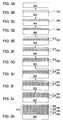
- FIG. 1illustrates a process sequence for forming a dielectric material according to one embodiment described herein;
- FIGS. 2A-2Iillustrate a process sequence for depositing multiple layers on a substrate surface according to another embodiment described herein;
- FIGS. 3A-3Killustrate another process sequence for depositing multiple layers on a substrate surface according to another embodiment described herein;
- FIG. 4illustrates a process sequence for forming a dielectric material according to another embodiment described herein.
- FIGS. 5A-5Dillustrate a process sequence for forming multiple layers on a substrate surface according to another embodiment described herein.
- the present inventionprovides methods for preparing dielectric materials used in a variety of applications, especially for high-k dielectric materials used in transistor and/or capacitor fabrication. Some of the methods use atomic layer deposition (ALD) to have elemental control of the composition of the dielectric compounds.
- ALDatomic layer deposition
- a dielectric materialis formed by conducting multiple cycles of a deposition process that include depositing a dielectric layer, exposing the dielectric layer to a nitridation process and optionally exposing the dielectric layer to an anneal process. The deposition process is repeated until the dielectric material has a desired thickness.
- a dielectric materialis formed by depositing a dielectric film and subsequently exposing the dielectric film to a nitridation process and an anneal process. The dielectric film is usually a metal oxide and substantially silicon-free.
- a “substrate surface” as used hereinrefers to any substrate or material surface formed on a substrate upon which film processing is performed.
- a substrate surface on which processing may be performedinclude materials such as dielectric materials, silicon, silicon oxide, strained silicon, silicon on insulator (SOI), carbon doped silicon oxides, silicon nitride, doped silicon, germanium, gallium arsenide, glass, sapphire, and any other materials such as metals, metal nitrides, metal alloys, and other conductive materials, depending on the application.
- Barrier layers, metals or metal nitrides on a substrate surfaceinclude titanium, titanium nitride, tungsten nitride, tantalum and tantalum nitride.
- Substratesmay have various dimensions, such as 200 mm or 300 mm diameter wafers, as well as, rectangular or square panes. Embodiments of the processes described herein deposit silicon-containing compounds on many substrates and surfaces, especially, high-k dielectric materials. Substrates on which embodiments of the invention may be useful include, but are not limited to semiconductor wafers, such as crystalline silicon (e.g., Si ⁇ 100> or Si ⁇ 111>), silicon oxide, strained silicon, SOI, silicon germanium, doped or undoped polysilicon, doped or undoped silicon wafers silicon nitride and patterned or non-patterned wafers.
- semiconductor waferssuch as crystalline silicon (e.g., Si ⁇ 100> or Si ⁇ 111>), silicon oxide, strained silicon, SOI, silicon germanium, doped or undoped polysilicon, doped or undoped silicon wafers silicon nitride and patterned or non-patterned wafers.
- Surfacesinclude bare silicon wafers, films, layers and materials with dielectric, conductive and barrier properties and include aluminum oxide and polysilicon. Pretreatment of surfaces includes polishing, etching, reduction, oxidation, hydroxylation, annealing and/or baking.
- “Atomic layer deposition” or “cyclical deposition” as used hereinrefers to the sequential introduction of two or more reactive compounds to deposit a layer of material on a substrate surface.
- the two, three or more reactive compoundsmay alternatively be introduced into a reaction zone of a processing chamber.
- each reactive compoundis separated by a time delay to allow each compound to adhere and/or react on the substrate surface.
- a first precursor or compound Ais pulsed into the reaction zone followed by a first time delay.
- a second precursor or compound Bis pulsed into the reaction zone followed by a second delay.
- a purge gassuch as nitrogen, is introduced into the processing chamber to purge the reaction zone or otherwise remove any residual reactive compound or by-products from the reaction zone.
- the purge gasmay flow continuously throughout the deposition process so that only the purge gas flows during the time delay between pulses of reactive compounds.
- the reactive compoundsare alternatively pulsed until a desired film or film thickness is formed on the substrate surface.
- the ALD process of pulsing compound A, purge gas, pulsing compound B and purge gasis a cycle.
- a cyclecan start with either compound A or compound B and continue the respective order of the cycle until achieving a film with the desired thickness.
- a “pulse” as used hereinis intended to refer to a quantity of a particular compound that is intermittently or non-continuously introduced into a reaction zone of a processing chamber.
- the quantity of a particular compound within each pulsemay vary over time, depending on the duration of the pulse.
- the duration of each pulseis variable depending upon a number of factors such as, for example, the volume capacity of the process chamber employed, the vacuum system coupled thereto, and the volatility/reactivity of the particular compound itself.
- a “half-reaction” as used hereinis intended to refer to a pulse of precursor step followed by a purge step.
- FIG. 1illustrates an exemplary process 100 for forming a dielectric material, such as a hafnium silicon oxynitride material.
- FIGS. 2A-3Kcorrespond to process 100 to illustrate the formation of a dielectric material used in a semiconductor device, such as a transistor and/or capacitor. Multiple dielectric layers of the same or similar composition are deposited sequentially to form a dielectric material. Each dielectric layer is deposited with morphology of either an amorphous layer or a layer containing nanocrystalline material. The morphology depends on the thickness of each individual layer since the layer thickness essentially results in dimensional confinement of the material. If the confinement is small, that is, if the layer thickness is thin enough, then the layer may be forced to remain amorphous.
- a dielectric layer 202is deposited on a substrate 200 , in step 102 , by conventional deposition techniques, such as ALD, chemical vapor deposition (CVD), physical vapor deposition (PVD), thermal techniques and combinations thereof, as depicted in FIGS. 2A-2B .
- dielectric layer 202is deposited by an ALD process and apparatus, such as described in co-pending United States Provisional Patent Application Serial No. unknown, filed May 12, 2004, entitled, “Atomic Layer Deposition of Hafnium-containing High-K Materials,” assigned to Applied Materials, Inc., and is herein incorporated by reference.
- Dielectric layer 202is generally deposited with a film thickness from about 1 ⁇ to about 50 ⁇ , preferably from about 5 ⁇ to about 30 ⁇ and more preferably from about 5 ⁇ to about 20 ⁇ , for example, about 15 ⁇ .
- a pretreatmentis especially useful prior to depositing dielectric layer 202 with an ALD process or a CVD process.
- a pretreatmentmay be effected by administering a reagent, such as NH 3 , B 2 H 6 , SiH 4 , Si 2 H 6 , H 2 O, HF, HCl, O 2 , O 3 , H 2 O, H 2 O/O 2 , H 2 O/H 2 , H 2 O 2 , H 2 , atomic-H, atomic-N, atomic-O, alcohols or amines.
- a reagentsuch as NH 3 , B 2 H 6 , SiH 4 , Si 2 H 6 , H 2 O, HF, HCl, O 2 , O 3 , H 2 O, H 2 O/O 2 , H 2 O/H 2 , H 2 O 2 , H 2 , atomic-H, atomic-N, atomic-O, alcohols or amines.
- the pretreatmentmay involve a presoak with a reagent prior to depositing a hafnium compound.
- the presoakmay involve exposing the substrate surface to the reagent for a period of time from about 5 seconds to about 120 seconds, preferably from about 5 seconds to about 30 seconds.
- the substrate surfaceis exposed to water vapor for about 15 seconds prior to starting an ALD process to deposit dielectric layer 202 .
- Dielectric layer 202is generally a high-k dielectric material and includes combinations of hafnium, zirconium, titanium, tantalum, lanthanum, aluminum, silicon, oxygen and/or nitrogen.
- Dielectric layer 202may have a composition that includes hafnium-containing materials, such as hafnium oxides (HfO x or HfO 2 ), hafnium silicates (HfSi x O y or HfSiO 4 ), hafnium silicon oxynitrides (HfSi x O y N z ), hafnium oxynitrides (HfO x N y ), hafnium aluminates (HfAl x O y ), hafnium aluminum silicates (HfAl x Si y O z ), hafnium aluminum silicon oxynitrides (HfAl w Si x O y N z ), hafnium lanthanum oxides (HfLa
- dielectric materials useful for dielectric layer 202may include titanium oxides (TiO x or TiO 2 ), titanium oxynitrides (TiO x N y ), tantalum oxides (TaO x or Ta 2 O 5 ) and tantalum oxynitrides (TaO x N y ).
- the dielectric layer 202is exposed to a nitridation process that physically incorporates nitrogen atoms into the dielectric material to form nitrogen-containing dielectric layer 204 , as depicted in FIG. 2C .
- the nitridation processmay include decoupled plasma nitridation (DPN), remote plasma nitridation, hot-wired induced atomic-N, and nitrogen incorporation during the dielectric layer deposition (e.g., during ALD or CVD processes).
- the nitrogen-containing dielectric layer 204is usually nitrogen-rich at the surface.
- the nitrogen concentration of nitrogen-containing dielectric layer 204may be in the range from about 5 atomic percent (at %) to about 40 at %, preferably from about 10 at % to about 25 at %.
- the nitridation processexposes the dielectric layer 202 to nitrogen plasma, such as a DPN process.
- the substrateis transferred to a DPN chamber, such as the CENTURATM DPN chamber, available from Applied Materials, Inc., located in Santa Clara, Calif.
- the DPN chamberis on the same cluster tool as the ALD chamber used to deposit the dielectric layer 202 . Therefore, the substrate may be exposed to a nitridation process without being exposed to the ambient environment.
- the dielectric layer 202is bombarded with atomic-N formed by co-flowing N 2 and a noble gas plasma, such as argon.
- nitrogen-containing gasesmay be used to form the nitrogen plasma, such as NH 3 , hydrazines (e.g., N 2 H 4 or MeN 2 H 3 ), amines (e.g., Me 3 N, Me 2 NH or MeNH 2 ), anilines (e.g., C 6 H 5 NH 2 ), and azides (e.g., MeN 3 or Me 3 SiN 3 ).
- Other noble gases that may be used in a plasma processinclude helium, neon and xenon.
- the nitridation processproceeds at a time period from about 10 seconds to about 120 seconds, preferably from about 15 seconds to about 60 seconds, for example, about 30 seconds.
- the nitridation processis conducted at a plasma power setting from about 900 watts to about 2,700 watts and a pressure at about 10 mTorr to about 100 mTorr.
- the nitrogenhas a flow from about 0.1 slm to about 1.0 slm, while the noble gas has a flow from about 0.1 slm to about 1.0 slm.
- the nitridation processis a DPN process and includes a plasma by co-flowing Ar and N 2 .
- a nitridation processmay include exposing the dielectric layer 202 to nitrogen plasma in the same deposition chamber that dielectric layer 202 is deposited.
- a nitridizing remote-plasmais exposed to dielectric layer 202 to form nitrogen-containing dielectric layer 204 directly in process chamber configured with a remote-plasma device, such as an ALD chamber or a CVD chamber.
- Radical nitrogen compoundsmay also be produced by heat or hot-wires and used during nitridation processes.
- nitrogen-containing dielectric layer 204Other nitridation processes to form nitrogen-containing dielectric layer 204 are contemplated, such as annealing the substrate in a nitrogen-containing environment, and/or including a nitrogen precursor into an additional half reaction within the ALD cycle while forming the nitrogen-containing dielectric layer 204 .
- an additional half reaction during an ALD cycle to form hafnium silicatemay include a pulse of NH 3 followed by a pulse of purge gas.
- the optional anneal processis omitted during step 106 .
- the predetermined thickness of dielectric materialis decided. If, after one cycle of steps 102 - 106 , the predetermined thickness of dielectric material is achieved, then process 100 may endure an optional anneal process at step 110 and process 100 is ended at step 112 . However, in the preferred embodiment, the dielectric material thickness is not achieved after only one cycle of steps 102 - 106 and therefore is repeated by starting over at step 102 .
- dielectric layer 212is deposited on nitrogen-containing dielectric layer 204 by the same process as discussed in step 102 .
- the layer thickness of dielectric layer 212does not have to be the same thickness as dielectric layer 202 , but generally have similar thicknesses.
- dielectric layer 212is exposed to a nitridation process as discussed in step 104 to form nitrogen-containing dielectric layer 214 .
- dielectric layer 222is deposited on nitrogen-containing dielectric layer 214 by the same process as discussed in step 102 .
- dielectric layer 222is exposed to a nitridation process as discussed in step 104 to form nitrogen-containing dielectric layer 224 . Steps 102 - 106 may be repeated to form the predetermined thickness of the dielectric material.
- FIG. 2Hdepicts a stack 260 of nitrogen-containing dielectric layers 204 , 214 , 224 , 234 , 244 and 254 after steps 102 - 106 have been performed six times. Thereafter, if the predetermined thickness of dielectric material is achieved during step 108 , the substrate is exposed to the optional anneal process during step 110 .
- the substrateis transferred to an anneal chamber, such as the CENTURATM RADIANCETM RTP chamber available from Applied Materials, Inc., located in Santa Clara, Calif., and exposed to an anneal process.
- the anneal chambermay be on the same cluster tool as the deposition chamber and/or the nitridation chamber. Therefore, the substrate may be annealed without being exposed to the ambient environment.
- the substrateis maintained at a temperature from about 600° C. to about 1,200° C. for a time period from about 1 second to about 120 seconds, for example, at about 1,000° C. for about 15 seconds.
- the process chamber atmospherecontains at least one anneal gas, such as O 2 , N 2 , NH 3 , N 2 H 4 , NO, N 2 O, or combinations thereof.
- the chamberis maintained at a pressure from about 1 Torr to about 100 Torr, for example, at about 5 Torr.
- the anneal processconverts stack 260 to the dielectric material or stack 270 , which contains dielectric nitride material layers 206 , 216 , 226 , 236 , 246 and 256 , as depicted in FIG. 2I .
- the anneal processrepairs any damage caused by plasma bombardment during step 104 and reduces the fixed charge of the dielectric nitride layers.
- Each of the dielectric nitride material layers 206 , 216 , 226 , 236 , 246 and 256may have a film thickness from about 1 ⁇ to about 50 ⁇ , preferably from about 5 ⁇ to about 30 ⁇ and more preferably from about 5 ⁇ to about 20 ⁇ , for example, about 15 ⁇ .
- Dielectric material or stack 270generally has a thickness from about 10 ⁇ to about 250 ⁇ , preferably from about 20 ⁇ to about 100 ⁇ , for example, 60 ⁇ . In one embodiment, dielectric material or stack 270 has a thickness of 60 ⁇ or less.
- a dielectric layer 302is deposited on a substrate 300 , in step 102 , by conventional deposition techniques, such as ALD, chemical vapor deposition (CVD), physical vapor deposition (PVD), thermal techniques and combinations thereof, as depicted in FIGS. 3A-3B .
- dielectric layer 302is deposited by an ALD process, as discussed above for dielectric layer 202 .
- Dielectric layer 302is generally a high-k dielectric material and includes combinations of hafnium, zirconium, titanium, tantalum, lanthanum, aluminum, silicon, oxygen and/or nitrogen.
- Dielectric layer 302may have the composition as dielectric layer 202 , as discussed above.
- Dielectric layer 302is generally deposited with a film thickness from about 1 ⁇ to about 50 ⁇ , preferably from about 5 ⁇ to about 30 ⁇ and more preferably from about 5 ⁇ to about 20 ⁇ , for example, about 15 ⁇ .
- the dielectric layer 302is exposed to a nitridation process that physically incorporates nitrogen atoms into dielectric film to form nitrogen-containing dielectric layer 304 , as depicted in FIG. 3C .
- the nitridation processmay include decoupled plasma nitridation (DPN), remote plasma nitridation, hot-wired induced atomic-N, and nitrogen incorporation during dielectric deposition (e.g., during ALD or CVD processes).
- the nitrogen-containing dielectric layer 304is usually nitrogen-rich at the surface.
- the nitrogen concentration of nitrogen-containing dielectric layer 304may be in the range from about 5 at % to about 40 at %, preferably from about 10 at % to about 25 at %.
- the nitridation processexposes the dielectric layer 302 to nitrogen plasma, such as a DPN process.
- the substrateis transferred to a DPN chamber, such as the CENTURATM DPN chamber, available from Applied Materials, Inc., located in Santa Clara, Calif.
- the DPN chamberis on the same cluster tool as the ALD chamber used to deposit the dielectric layer 302 . Therefore, the substrate may be exposed to a nitridation process without being exposed to the ambient environment.
- the dielectric layer 302is bombarded with atomic-N formed by co-flowing N 2 and a noble gas plasma, such as argon.
- nitrogen-containing gasesmay be used to form the nitrogen plasma, such as NH 3 , hydrazines (e.g., N 2 H 4 or MeN 2 H 3 ), amines (e.g., Me 3 N, Me 2 NH or MeNH 2 ), anilines (e.g., C 6 H 5 NH 2 ), and azides (e.g., MeN 3 or Me 3 SiN 3 ).
- Other noble gases that may be used in a plasma processinclude helium, neon and xenon.
- the nitridation processproceeds at a time period from about 10 seconds to about 120 seconds, preferably from about 15 seconds to about 60 seconds, for example, about 30 seconds.
- the nitridation processis conducted at a plasma power setting from about 900 watts to about 2,700 watts and a pressure at about 10 mTorr to about 100 mTorr.
- the nitrogenhas a flow from about 0.1 slm to about 1.0 slm, while the noble gas has a flow from about 0.1 slm to about 1.0 slm.
- the nitridation processis a DPN process and includes a plasma by co-flowing Ar and N 2 .
- a nitridation processmay include exposing the dielectric layer 302 to nitrogen plasma in the same deposition chamber that dielectric layer 302 is deposited.
- a nitrogen remote-plasmais exposed to dielectric layer 302 to form nitrogen-containing dielectric layer 304 directly in process chamber configured with a remote-plasma device, such as an ALD chamber or a CVD chamber.
- Radical nitrogen compoundsmay also be produced by heat or hot-wires and used during nitridation processes.
- nitrogen-containing dielectric layer 304Other nitridation processes to form nitrogen-containing dielectric layer 304 are contemplated, such as annealing the substrate in a nitrogen-containing environment, and/or including a nitrogen precursor into an additional half reaction within the ALD cycle while forming the nitrogen-containing dielectric layer 304 .
- an additional half reaction during an ALD cycle to form hafnium silicatemay include a pulse of NH 3 followed by a pulse of purge gas.
- the optional anneal processis executed during step 106 .
- the substrateis transferred to an anneal chamber, such as the CENTURATM RADIANCETM RTP chamber available from Applied Materials, Inc., located in Santa Clara, Calif., and exposed to an anneal process.
- the anneal chambermay be on the same cluster tool as the deposition chamber and/or the nitridation chamber. Therefore, the substrate may be annealed without being exposed to the ambient environment
- the substrateis maintained at a temperature from about 600° C. to about 1,200° C. for a time period from about 1 second to about 120 seconds, for example, at about 1,000° C. for about 15 seconds.
- the process chamber atmospherecontains at least one anneal gas, such as O 2 , N 2 , NH 3 , N 2 H 4 , NO, N 2 O, or combinations thereof.
- the chamberis maintained at a pressure from about 1 Torr to about 100 Torr, for example, about 5 Torr.
- the anneal processconverts nitrogen-containing dielectric layer 304 to dielectric nitride material layers 306 , as depicted in FIG. 3D .
- the anneal processrepairs any damage caused by plasma bombardment during step 104 and reduces the fixed charge of nitrogen-containing dielectric layer 304 .
- the predetermined thickness of dielectric materialis decided. If, after one cycle of steps 102 - 106 , the predetermined layer thickness of the dielectric material is achieved, then process 100 skips the optional anneal process during step 110 and is ended during step 112 . However, in the preferred embodiment, the dielectric material thickness is not achieved after only one cycle of steps 102 - 106 and therefore is repeated.
- dielectric layer 312is deposited on dielectric nitride layer 306 by the same process as discussed in step 102 .
- the layer thickness of dielectric layer 312does not have to be the same thickness as dielectric layer 302 , but generally have similar thicknesses.
- dielectric layer 312is exposed to a nitridation process as discussed in step 104 to form nitrogen-containing dielectric layer 314 .
- the substrateis exposed to an anneal process as discussed in step 106 to convert nitrogen-containing dielectric layer 314 to dielectric nitride layer 316 .
- dielectric layer 322is deposited on dielectric nitride layer 316 by the same process as discussed in step 102 .
- dielectric layer 322is exposed to a nitridation process as discussed in step 104 to form nitrogen-containing dielectric layer 324 .
- the substrateis exposed to an anneal process in step 106 to convert nitrogen-containing dielectric layer 324 to dielectric nitride layer 326 . Steps 102 - 106 may be repeated to form the predetermined thickness of the dielectric material.
- FIG. 3Kdepicts dielectric material or stack 370 of dielectric nitride material layers 306 , 316 , 326 , 336 , 346 and 356 after steps 102 - 106 have been performed six times.
- Each of the dielectric nitride material layers 306 , 316 , 326 , 336 , 346 and 356may have a film thickness from about 1 ⁇ to about 50 ⁇ , preferably from about 5 ⁇ to about 30 ⁇ and more preferably from about 5 ⁇ to about 20 ⁇ , for example, about 15 ⁇ .
- Dielectric material or stack 370generally has a thickness from about 10 ⁇ to about 250 ⁇ , preferably from about 20 ⁇ to about 100 ⁇ , for example, 60 ⁇ . In one embodiment, dielectric material or stack 370 has a thickness 60 ⁇ or less.
- FIGS. 2I and 3 kdepict stacks 270 and 370 containing six dielectric nitride material layers, numerous layers may be deposited in order to form a dielectric material.
- a dielectric materialmay have as few as two layers or hundreds of layers.
- a dielectric material formed with an overall thickness of about 60 ⁇may include twelve 5 ⁇ dielectric layers, six 10 ⁇ dielectric layers, four 15 ⁇ dielectric layers, three 20 ⁇ dielectric layers or two 30 ⁇ dielectric layers, among others.
- a dielectric material formed with an overall thickness of about 100 ⁇may include twenty 5 ⁇ dielectric layers, ten 10 ⁇ dielectric layers, five 20 ⁇ dielectric layers, four 25 ⁇ dielectric layers or two 50 ⁇ dielectric layers, among others.
- Dielectric materialremains amorphous and may have a nitrogen concentration in the range from about 5 at % to about 25 at %, preferably from about 10 at % to about 20 at %, for example, about 15 at %.
- dielectric material or stack 270is formed by annealing the substrate after the desired number of dielectric layers is deposited or after the predetermined film thickness is achieved.
- dielectric material or stack 370is formed by annealing the substrate after each nitridation of the dielectric layers.
- the optional anneal process of step 106may be applied during a cycle of steps 102 - 106 and omitted during another cycle of steps 102 - 106 during the formation of a dielectric material. Routine experimentation may be conducted to determine the correct intervals of exposing the substrate to the anneal process. Some variables that direct the annealing intervals include the specific nitridation technique used during the nitridation process, thickness and composition of dielectric layers and desired characteristics of the final dielectric material.
- FIG. 4illustrates an exemplary process 400 for forming a dielectric material, such as a hafnium oxynitride material or a tantalum oxynitride material.
- FIGS. 5A-5Dcorrespond to process 400 to illustrate the formation of a dielectric material used in of a semiconductor device, such as a transistor and/or capacitor.
- Dielectric layer 502disposed on substrate 500 , is exposed to a nitridation process to form nitrogen-containing dielectric layer 504 .
- nitrogen-containing dielectric layer 504is converted to dielectric nitride dielectric layer 506 by exposure to an anneal process.
- a dielectric layer 502is deposited on a substrate 500 , during step 402 , by conventional deposition techniques, such as ALD, CVD, PVD, thermal techniques and combinations thereof, as depicted in FIGS. 5A-5B .
- dielectric layer 502is deposited by an ALD process and apparatus, such as described in co-pending United States Provisional Patent Application Serial No. unknown, filed May 12, 2004, entitled, “Atomic Layer Deposition of Hafnium-containing High-K Materials,” assigned to Applied Materials, Inc., and is herein incorporated by reference.
- Dielectric layer 502is generally deposited with a film thickness from about 5 ⁇ to about 300 ⁇ , preferably from about 10 ⁇ to about 200 ⁇ and more preferably from about 10 ⁇ to about 100 ⁇ , for example, about 50 ⁇ .
- a pretreatmentis especially useful prior to depositing dielectric layer 502 with an ALD process or a CVD process.
- a pretreatmentmay be effected by administering a reagent, such as NH 3 , B 2 H 6 , SiH 4 , Si 2 H 6 , H 2 O, HF, HCl, O 2 , O 3 , H 2 O, H 2 O/O 2 , H 2 O/H 2 , H 2 O 2 , H 2 , atomic-H, atomic-N, atomic-O, alcohols or amines.
- a reagentsuch as NH 3 , B 2 H 6 , SiH 4 , Si 2 H 6 , H 2 O, HF, HCl, O 2 , O 3 , H 2 O, H 2 O/O 2 , H 2 O/H 2 , H 2 O 2 , H 2 , atomic-H, atomic-N, atomic-O, alcohols or amines.
- the pretreatmentmay involve a presoak with a reagent prior to depositing a hafnium compound.
- the presoakmay involve exposing the substrate surface to the reagent for a period of time from about 5 seconds to about 120 seconds, preferably from about 5 seconds to about 30 seconds.
- the substrate surfaceis exposed to water for about 15 seconds prior to starting an ALD process to deposit dielectric layer 502 .
- Dielectric layer 502is deposited on the substrate surface and may have a variety of compositions that are homogenous, heterogeneous, graded and/or multiple layered stacks or laminates.
- Dielectric layer 502is generally a high-k dielectric material and includes combinations of hafnium, zirconium, titanium, tantalum, lanthanum, aluminum, oxygen and/or nitrogen. Often a metal oxide or a metal oxynitride is used as dielectric layer 502 . Although some silicon diffusion into dielectric layer 502 may occur from the substrate, dielectric layer 502 is usually substantially free of silicon.
- Dielectric layer 502may have a composition that includes hafnium-containing materials, such as hafnium oxides (HfO x or HfO 2 ), hafnium oxynitrides (HfO x N y ), hafnium aluminates (HfAl x O y ), hafnium lanthanum oxides (HfLa x O y ), zirconium-containing materials, such as zirconium oxides (ZrO x or ZrO 2 ), zirconium oxynitrides (ZrO x N y ), zirconium aluminates (ZrAl x O y ), zirconium lanthanum oxides (ZrLa x O y ), other aluminum-containing materials or lanthanum-containing materials, such as aluminum oxides (Al 2 O 3 or AlO x ), aluminum oxynitrides (AlO x N y ), lanthanum aluminum oxides (LaA
- dielectric materials useful for dielectric layer 502may include titanium oxides (TiO x or TiO 2 ), titanium oxynitrides (TiO x N y ), tantalum oxides (TaO x or Ta 2 O 5 ) and tantalum oxynitrides (TaO x N y ).
- Laminate films that are useful dielectric materials for dielectric layer 502include HfO 2 /Al 2 O 3 , La 2 O 3 Al 2 O 3 and HfO 2 /La 2 O 3 /Al 2 O 3 .
- the dielectric layer 502is exposed to a nitridation process that physically incorporates nitrogen atoms into the dielectric to form nitrogen-containing dielectric layer 504 , as depicted in FIG. 5C .
- the nitridation processmay include decoupled plasma nitridation (DPN), remote plasma nitridation, hot-wired induced atomic-N, and nitrogen incorporation during dielectric deposition (e.g., during ALD or CVD processes).
- the nitrogen-containing dielectric layer 504is usually nitrogen-rich at the surface.
- the nitrogen concentration of nitrogen-containing dielectric layer 504may be in the range from about 5 at % to about 40 at %, preferably from about 10 at % to about 25 at %.
- the nitridation processexposes the dielectric layer 502 to nitrogen plasma, such as a DPN process.
- the substrateis transferred to a DPN chamber, such as the CENTURATM DPN chamber, available from Applied Materials, Inc., located in Santa Clara, Calif.
- the DPN chamberis on the same cluster tool as the ALD chamber used to deposit the dielectric layer 502 . Therefore, the substrate may be exposed to a nitridation process without being exposed to the ambient environment.
- the dielectric layer 502is bombarded with atomic-N formed by co-flowing N 2 and a noble gas plasma, such as argon.
- nitrogen-containing gasesmay be used to form the nitrogen plasma, such as NH 3 , hydrazines (e.g., N 2 H 4 or MeN 2 H 3 ), amines (e.g., Me 3 N, Me 2 NH or MeNH 2 ), anilines (e.g., C 6 H 5 NH 2 ), and azides (e.g., MeN 3 or Me 3 SiN 3 ).
- Other noble gases that may be used in a plasma processinclude helium, neon and xenon.
- the nitridation processproceeds at a time period from about 10 seconds to about 120 seconds, preferably from about 15 seconds to about 60 seconds, for example, about 30 seconds.
- the nitridation processis conducted at a plasma power setting from about 900 watts to about 2,700 watts and a pressure at about 10 mTorr to about 100 mTorr.
- the nitrogenhas a flow from about 0.1 slm to about 1.0 slm, while the noble gas has a flow from about 0.1 slm to about 1.0 slm.
- the nitridation processis a DPN process and includes a plasma by co-flowing Ar and N 2 .
- a nitridation processmay include exposing the dielectric layer 502 to nitrogen plasma in the same deposition chamber that dielectric layer 502 is deposited.
- a nitrogen remote-plasmais exposed to dielectric layer 502 to form nitrogen-containing dielectric layer 504 directly in process chamber configured with a remote-plasma device, such as an ALD chamber or a CVD chamber.
- Radical nitrogen compoundsmay also be produced by heat or hot-wires and used during nitridation processes.
- nitrogen-containing dielectric layer 504Other nitridation processes to form nitrogen-containing dielectric layer 504 are contemplated, such as annealing the substrate in a nitrogen-containing environment, and/or including a nitrogen precursor into an additional half reaction within the ALD cycle while forming the nitrogen-containing dielectric layer 504 .
- an additional half reaction during an ALD cycle to form hafnium oxidemay include a pulse of NH 3 followed by a pulse of purge gas.
- the substrateis exposed to an anneal process.
- the substrateis transferred to an anneal chamber, such as the CENTURATM RADIANCETM RTP chamber available from Applied Materials, Inc., located in Santa Clara, Calif., and exposed to an anneal process.
- the anneal chambermay be on the same cluster tool as the deposition chamber and/or the nitridation chamber. Therefore, the substrate may be annealed without being exposed to the ambient environment.
- the substrateis maintained at a temperature from about 600° C. to about 1,200° C. for a time period from about 1 second to about 120 seconds, for example, at about 1,000° C. for about 60 seconds.
- the process chamber atmospherecontains at least one anneal gas, such as O 2 , N 2 , NH 3 , N 2 H 4 , NO, N 2 O, or combinations thereof.
- the chamberis maintained at a pressure from about 5 Torr to about 100 Torr, for example, at about 5 Torr.
- the anneal processconverts nitrogen-containing dielectric layer 504 to the dielectric material or dielectric nitride layer 506 , as depicted in FIG. 5D .
- the anneal processrepairs any damage caused by plasma bombardment during step 404 and reduces the fixed charge of dielectric nitride layer 506 .
- Dielectric materialremains amorphous and may have a nitrogen concentration in the range from about 5 at % to about 25 at %, preferably from about 10 at % to about 20 at %, for example, about 15 at %.
- Dielectric nitride layer 506has a film thickness from about 5 ⁇ to about 300 ⁇ , preferably from about 10 ⁇ to about 200 ⁇ and more preferably from about 10 ⁇ to about 100 ⁇ , for example, about 50 ⁇ .
- a substrateis placed into an ALD chamber and the substrate surface is exposed to a pretreatment to form hydroxyl groups.
- a hafnium silicate layeris deposited on the substrate surface by performing an ALD process using the hafnium precursor (HfCl 4 ), the silicon precursor (TDMAS), and in-situ water vapor produced by a water vapor generator (WVG) system, available from Fujikin of America, Inc., located in Santa Clara, Calif.
- the ALD cycleincludes sequentially pulsing HfCl 4 , water vapor, TDMAS and water vapor, with each precursor separated by a nitrogen purge cycle.
- the ALD cycleis repeated ten times to form a hafnium silicate layer with a thickness of about 4 ⁇ .
- the substrateis transferred to a decoupled plasma nitridation (DPN) chamber, such as the CENTURATM DPN chamber, available from Applied Materials, Inc., located in Santa Clara, Calif.
- DPNdecoupled plasma nitridation
- the substrate surfaceis exposed to a nitridation process by co-flowing N 2 with an argon plasma.
- the nitridation processproceeds for about 10 seconds to incorporate nitrogen atoms within the hafnium silicate layer.
- the substrateis subsequently transferred to an anneal chamber, such as the CENTURATM RADIANCETM RTP chamber available from Applied Materials, Inc., located in Santa Clara, Calif., and exposed to an anneal process.
- the substrateis maintained at about 1,000° C. for about 15 seconds in an O 2 atmosphere maintained at about 15 Torr.
- the incorporated nitrogen atomsform bonds with the hafnium silicate to produce hafnium silicon oxynitride.
- the process cycle containing the ALD process, the nitridation process and the anneal processis repeated fifteen times to form a hafnium silicon oxynitride layer with a thickness of about 60 ⁇ .
- a substrateis placed into an ALD chamber equipped with a remote plasma generator and the substrate surface is exposed to a pretreatment to form hydroxyl groups.
- a hafnium silicate layeris deposited on the substrate surface by performing an ALD process using the hafnium precursor (TDEAH), the silicon precursor (Tris-DMAS), and in-situ water vapor produced by a water vapor generator (WVG) system, available from Fujikin of America, Inc., located in Santa Clara, Calif.
- the ALD cycleincludes co-flowing TDEAH and Tris-DMAS in a first half reaction and sequentially pulsing water vapor in a second half reaction, with each half reaction separated by an argon purge.
- the hafnium silicate layeris formed by repeating the cycle ten times until the film has a thickness of about 4 ⁇ .
- the ALD processis stopped and the substrate is kept in the ALD chamber equipped with a remote plasma generator.
- the substrate surfaceis exposed to a remote plasma nitridation process for about 10 seconds to incorporate nitrogen atoms within the hafnium silicate layer.
- the substrateis subsequently transferred to an anneal chamber, such as the CENTURATM RADIANCETM RTP chamber available from Applied Materials, Inc., located in Santa Clara, Calif., and exposed to an anneal process.
- the substrateis maintained at about 1,000° C. for about 15 seconds in an O 2 atmosphere maintained at about 15 Torr.
- the incorporated nitrogen atomsform bonds with the hafnium silicate to produce hafnium silicon oxynitride.
- the process cycle containing the ALD process, the nitridation process and the anneal processis repeated fifteen times to form a hafnium silicon oxynitride layer with a thickness of about 60 ⁇ .
- a substrateis placed into an ALD chamber and the substrate surface is exposed to a pretreatment to form hydroxyl groups.
- a tantalum oxide layeris deposited on the substrate surface by performing an ALD process using the tantalum precursor (TaCl 5 ) and water.
- the ALD cycleincludes sequentially pulsing TaCl 5 and water vapor with each precursor separated by a nitrogen purge cycle.
- the ALD cycleis repeated eight times to form a tantalum oxide layer with a thickness of about 5 ⁇ .
- the substrateis transferred to a decoupled plasma nitridation (DPN) chamber, such as the CENTURATM DPN chamber, available from Applied Materials, Inc., located in Santa Clara, Calif.
- DPNdecoupled plasma nitridation
- the substrate surfaceis exposed to a nitridation process by co-flowing N 2 with an argon plasma.
- the nitridation processproceeds for about 10 seconds to incorporate nitrogen atoms within the tantalum oxide layer.
- the substrateis subsequently transferred to an anneal chamber, such as the CENTURATM RADIANCETM RTP chamber available from Applied Materials, Inc., located in Santa Clara, Calif., and exposed to an anneal process.
- the substrateis maintained at about 1,000° C. for about 15 seconds in an O 2 atmosphere maintained at about 15 Torr.
- the incorporated nitrogen atomsform bonds with the tantalum oxide to produce tantalum oxynitride.
- the process cycle containing the ALD process, the nitridation process and the anneal processis repeated twenty times to form a tantalum oxynitride layer with a thickness of about 100 ⁇ .
- a substrateis placed into an ALD chamber equipped with a remote plasma generator and the substrate surface is exposed to a pretreatment to form hydroxyl groups.
- a tantalum oxide layeris deposited on the substrate surface by performing an ALD process using the tantalum precursor (TaCl 5 ) and water.
- the ALD cycleincludes sequentially pulsing TaCl 5 and water vapor with each precursor separated by a nitrogen purge cycle.
- the ALD cycleis repeated eight times to form a tantalum oxide layer with a thickness of about 5 ⁇ .
- the ALD processis stopped and the substrate is kept in the ALD chamber equipped with a remote plasma generator.
- the substrate surfaceis exposed to a remote plasma nitridation process for about 10 seconds to incorporate nitrogen atoms within the tantalum oxide layer.
- the substrateis subsequently transferred to an anneal chamber, such as the CENTURATM RADIANCETM RTP chamber available from Applied Materials, Inc., located in Santa Clara, Calif., and exposed to an anneal process.
- the substrateis maintained at about 1,000° C. for about 15 seconds in an O 2 atmosphere maintained at about 15 Torr.
- the incorporated nitrogen atomsform bonds with the tantalum oxide to produce tantalum oxynitride.
- the process cycle containing the ALD process, the nitridation process and the anneal processis repeated ten times to form a tantalum oxynitride layer with a thickness of about 50 ⁇ .
- a substrateis placed into an ALD chamber and the substrate surface is exposed to a pretreatment to form hydroxyl groups.
- a hafnium silicate layeris deposited on the substrate surface by performing an ALD process using the hafnium precursor (HfCl 4 ), the silicon precursor (TDMAS), and in-situ water vapor produced by a water vapor generator (WVG) system, available from Fujikin of America, Inc., located in Santa Clara, Calif.
- the ALD cycleincludes sequentially pulsing HfCl 4 , water vapor, TDMAS and water vapor, with each precursor separated by a nitrogen purge cycle.
- the ALD cycleis repeated ten times to form a hafnium silicate layer with a thickness of about 4 ⁇ .
- the substrateis transferred to a decoupled plasma nitridation (DPN) chamber, such as the CENTURATM DPN chamber, available from Applied Materials, Inc., located in Santa Clara, Calif.
- DPNdecoupled plasma nitridation
- the substrate surfaceis exposed to a nitridation process by co-flowing N 2 with an argon plasma.
- the nitridation processproceeds for about 10 seconds to incorporate nitrogen atoms within the hafnium silicate layer.
- the process cycle containing the ALD process and the nitridation processis repeated fifteen times to form a nitrated hafnium silicate layer with a thickness of about 60 ⁇ .
- the substrateis subsequently transferred to an anneal chamber, such as the CENTURATM RADIANCETM RTP chamber available from Applied Materials, Inc., located in Santa Clara, Calif., and exposed to an anneal process.
- the substrateis maintained at about 1,000° C. for about 60 seconds in an O 2 atmosphere maintained at about 15 Torr.
- the incorporated nitrogen atomsform bonds with the hafnium silicate to produce hafnium silicon oxynitride.
- a substrateis placed into an ALD chamber and the substrate surface is exposed to a pretreatment to form hydroxyl groups.
- a tantalum oxide layeris deposited on the substrate surface by performing an ALD process using the tantalum precursor (TaCl 5 ) and water.
- the ALD cycleincludes sequentially pulsing TaCl 5 and water vapor with each precursor separated by a nitrogen purge cycle.
- the ALD cycleis repeated eight times to form a tantalum oxide layer with a thickness of about 12 ⁇ .
- the substrateis transferred to a decoupled plasma nitridation (DPN) chamber, such as the CENTURATM DPN chamber, available from Applied Materials, Inc., located in Santa Clara, Calif.
- DPNdecoupled plasma nitridation
- the substrate surfaceis exposed to a nitridation process by co-flowing N 2 with an argon plasma.
- the nitridation processproceeds for about 10 seconds to incorporate nitrogen atoms within the tantalum oxide layer.
- the process cycle containing the ALD process and the nitridation processis repeated ten times to form a nitrided tantalum oxide layer with a thickness of about 120 ⁇ .
- the substrateis subsequently transferred to an anneal chamber, such as the CENTURATM RADIANCETM RTP chamber available from Applied Materials, Inc., located in Santa Clara, Calif. and exposed to an anneal process.
- the substrateis maintained at about 1,000° C. for about 60 seconds in an O 2 atmosphere maintained at about 15 Torr.
- the incorporated nitrogen atomsform bonds with the tantalum oxide to produce tantalum oxynitride.
- a substrateis placed into an ALD chamber and the substrate surface is exposed to a pretreatment to form hydroxyl groups.
- a hafnium oxide layeris deposited on the substrate surface by performing an ALD process using the hafnium precursor (HfCl 4 ) and water.
- the ALD cycleincludes sequentially pulsing HfCl 4 and water vapor with each precursor separated by a nitrogen purge cycle. The ALD cycle is repeated until a hafnium oxide layer was deposited with a thickness of about 75 ⁇ .
- the substrateis transferred to a decoupled plasma nitridation (DPN) chamber, such as the CENTURATM DPN chamber, available from Applied Materials, Inc., located in Santa Clara, Calif.
- DPNdecoupled plasma nitridation
- the substrate surfaceis exposed to a nitridation process by co-flowing N 2 with an argon plasma.
- the nitridation processproceeds for about 30 seconds to incorporate nitrogen atoms within the hafnium oxide layer.
- the substrateis subsequently transferred to an anneal chamber, such as the CENTURATM RADIANCETM RTP chamber available from Applied Materials, Inc., located in Santa Clara, Calif., and exposed to an anneal process.
- the substrateis maintained at about 1,000° C. for about 45 seconds in an O 2 atmosphere maintained at about 15 Torr.
- the incorporated nitrogen atomsform bonds with the hafnium oxide to produce hafnium oxynitride.
- a substrateis placed into an ALD chamber and the substrate surface is exposed to a pretreatment to form hydroxyl groups.
- a tantalum oxide layeris deposited on the substrate surface by performing an ALD process using the tantalum precursor (TaCl 5 ) and water.
- the ALD cycleincludes sequentially pulsing TaCl 5 and water vapor with each precursor separated by a nitrogen purge cycle. The ALD cycle is repeated until a tantalum oxide layer was deposited with a thickness of about 85 ⁇ .
- the substrateis transferred to a decoupled plasma nitridation (DPN) chamber, such as the CENTURATM DPN chamber, available from Applied Materials, Inc., located in Santa Clara, Calif.
- DPNdecoupled plasma nitridation
- the substrate surfaceis exposed to a nitridation process by co-flowing N 2 with an argon plasma.
- the nitridation processproceeds for about 30 seconds to incorporate nitrogen atoms within the tantalum oxide layer.
- the substrateis subsequently transferred to an anneal chamber, such as the CENTURATM RADIANCETM RTP chamber available from Applied Materials, Inc., located in Santa Clara, Calif. and exposed to an anneal process.
- the substrateis maintained at about 1,000° C. for about 45 seconds in an O 2 atmosphere maintained at about 15 Torr.
- the incorporated nitrogen atomsform bonds with the tantalum oxide to produce tantalum oxynitride.
- Hafnium oxidewas deposited on Substrates A and B under the identical process conditions.
- Substrate Awas placed into a DPN chamber, such as the CENTURATM DPN chamber, available from Applied Materials, Inc., located in Santa Clara, Calif., and exposed to a nitridation process.
- Subsequently, Substrate Awas placed into an anneal chamber, such as the CENTURATM RADIANCETM RTP chamber available from Applied Materials, Inc., located in Santa Clara, Calif., and exposed to an anneal process.
- Substrate Bwas not exposed to a nitridation process or an anneal process.
- Substrate Ahad a current density a magnitude lower than Substrate B, although both substrates had similar EOTs (effective oxide thickness). Furthermore, Substrate A, having already been annealed, is thermal more stable than Substrate B, which will crystallize upon exposure to elevated temperatures experienced in subsequent fabrication processes.
Landscapes
- Engineering & Computer Science (AREA)
- Chemical & Material Sciences (AREA)
- Physics & Mathematics (AREA)
- Condensed Matter Physics & Semiconductors (AREA)
- General Physics & Mathematics (AREA)
- Manufacturing & Machinery (AREA)
- Computer Hardware Design (AREA)
- Microelectronics & Electronic Packaging (AREA)
- Power Engineering (AREA)
- Chemical Kinetics & Catalysis (AREA)
- General Chemical & Material Sciences (AREA)
- Materials Engineering (AREA)
- Mechanical Engineering (AREA)
- Metallurgy (AREA)
- Organic Chemistry (AREA)
- Inorganic Chemistry (AREA)
- Plasma & Fusion (AREA)
- Formation Of Insulating Films (AREA)
- Insulated Gate Type Field-Effect Transistor (AREA)
- Semiconductor Integrated Circuits (AREA)
- Semiconductor Memories (AREA)
Abstract
Description
Claims (6)
Priority Applications (10)
| Application Number | Priority Date | Filing Date | Title |
|---|---|---|---|
| US10/851,514US8323754B2 (en) | 2004-05-21 | 2004-05-21 | Stabilization of high-k dielectric materials |
| PCT/US2005/016606WO2005117086A1 (en) | 2004-05-21 | 2005-05-12 | Stabilization of high-k dielectric materials |
| KR1020067026971AKR20070013338A (en) | 2004-05-21 | 2005-05-12 | Stabilization of High Fin Dielectric Materials |
| EP05747422AEP1747580A1 (en) | 2004-05-21 | 2005-05-12 | Stabilization of high-k dielectric materials |
| JP2007527300AJP2008500741A (en) | 2004-05-21 | 2005-05-12 | Stabilization of high dielectric constant dielectric materials |
| CNA2005800092360ACN1934685A (en) | 2004-05-21 | 2005-05-12 | Stabilization method of high-k dielectric materials |
| TW094115983ATW200539300A (en) | 2004-05-21 | 2005-05-17 | Stabilization of high-k dielectric materials |
| US11/167,070US20060019033A1 (en) | 2004-05-21 | 2005-06-24 | Plasma treatment of hafnium-containing materials |
| US11/223,896US20060062917A1 (en) | 2004-05-21 | 2005-09-09 | Vapor deposition of hafnium silicate materials with tris(dimethylamino)silane |
| US11/298,553US20060153995A1 (en) | 2004-05-21 | 2005-12-09 | Method for fabricating a dielectric stack |
Applications Claiming Priority (1)
| Application Number | Priority Date | Filing Date | Title |
|---|---|---|---|
| US10/851,514US8323754B2 (en) | 2004-05-21 | 2004-05-21 | Stabilization of high-k dielectric materials |
Related Child Applications (1)
| Application Number | Title | Priority Date | Filing Date |
|---|---|---|---|
| US11/167,070Continuation-In-PartUS20060019033A1 (en) | 2004-05-21 | 2005-06-24 | Plasma treatment of hafnium-containing materials |
Publications (2)
| Publication Number | Publication Date |
|---|---|
| US20050260357A1 US20050260357A1 (en) | 2005-11-24 |
| US8323754B2true US8323754B2 (en) | 2012-12-04 |
Family
ID=34969431
Family Applications (1)
| Application Number | Title | Priority Date | Filing Date |
|---|---|---|---|
| US10/851,514Expired - Fee RelatedUS8323754B2 (en) | 2004-05-21 | 2004-05-21 | Stabilization of high-k dielectric materials |
Country Status (7)
| Country | Link |
|---|---|
| US (1) | US8323754B2 (en) |
| EP (1) | EP1747580A1 (en) |
| JP (1) | JP2008500741A (en) |
| KR (1) | KR20070013338A (en) |
| CN (1) | CN1934685A (en) |
| TW (1) | TW200539300A (en) |
| WO (1) | WO2005117086A1 (en) |
Cited By (12)
| Publication number | Priority date | Publication date | Assignee | Title |
|---|---|---|---|---|
| US8962097B1 (en) | 2007-09-07 | 2015-02-24 | Edward Maxwell Yokley | Surface properties of polymeric materials with nanoscale functional coating |
| US9633839B2 (en) | 2015-06-19 | 2017-04-25 | Applied Materials, Inc. | Methods for depositing dielectric films via physical vapor deposition processes |
| US20170191759A1 (en)* | 2015-12-30 | 2017-07-06 | Mattson Technology, Inc. | Gas Flow Control for Millisecond Anneal System |
| US9941144B2 (en) | 2015-12-30 | 2018-04-10 | Mattson Technology, Inc. | Substrate breakage detection in a thermal processing system |
| US10262873B2 (en) | 2016-02-01 | 2019-04-16 | Mattson Technology, Inc. | Pre-heat processes for millisecond anneal system |
| US10359334B2 (en) | 2015-12-30 | 2019-07-23 | Mattson Technology, Inc. | Fluid leakage detection for a millisecond anneal system |
| US20200027996A1 (en)* | 2018-07-17 | 2020-01-23 | Renesas Electronics Corporation | Semiconductor device and a method of manufacturing the same |
| US10727140B2 (en) | 2015-12-30 | 2020-07-28 | Mattson Technology, Inc. | Preheat processes for millisecond anneal system |
| US10734262B2 (en) | 2015-12-30 | 2020-08-04 | Mattson Technology, Inc. | Substrate support in a millisecond anneal system |
| US10770309B2 (en) | 2015-12-30 | 2020-09-08 | Mattson Technology, Inc. | Features for improving process uniformity in a millisecond anneal system |
| US10957563B2 (en) | 2015-12-30 | 2021-03-23 | Mattson Technology, Inc. | Chamber wall heating for a millisecond anneal system |
| US10966286B2 (en) | 2015-12-30 | 2021-03-30 | Mattson Technology, Inc. | Nitrogen injection for ARC lamps |
Families Citing this family (152)
| Publication number | Priority date | Publication date | Assignee | Title |
|---|---|---|---|---|
| US6551929B1 (en) | 2000-06-28 | 2003-04-22 | Applied Materials, Inc. | Bifurcated deposition process for depositing refractory metal layers employing atomic layer deposition and chemical vapor deposition techniques |
| US7101795B1 (en) | 2000-06-28 | 2006-09-05 | Applied Materials, Inc. | Method and apparatus for depositing refractory metal layers employing sequential deposition techniques to form a nucleation layer |
| US7405158B2 (en) | 2000-06-28 | 2008-07-29 | Applied Materials, Inc. | Methods for depositing tungsten layers employing atomic layer deposition techniques |
| US6852167B2 (en) | 2001-03-01 | 2005-02-08 | Micron Technology, Inc. | Methods, systems, and apparatus for uniform chemical-vapor depositions |
| US9139906B2 (en) | 2001-03-06 | 2015-09-22 | Asm America, Inc. | Doping with ALD technology |
| US8026161B2 (en) | 2001-08-30 | 2011-09-27 | Micron Technology, Inc. | Highly reliable amorphous high-K gate oxide ZrO2 |
| US6936906B2 (en) | 2001-09-26 | 2005-08-30 | Applied Materials, Inc. | Integration of barrier layer and seed layer |
| US6916398B2 (en) | 2001-10-26 | 2005-07-12 | Applied Materials, Inc. | Gas delivery apparatus and method for atomic layer deposition |
| US7081271B2 (en) | 2001-12-07 | 2006-07-25 | Applied Materials, Inc. | Cyclical deposition of refractory metal silicon nitride |
| US6972267B2 (en) | 2002-03-04 | 2005-12-06 | Applied Materials, Inc. | Sequential deposition of tantalum nitride using a tantalum-containing precursor and a nitrogen-containing precursor |
| US7160577B2 (en) | 2002-05-02 | 2007-01-09 | Micron Technology, Inc. | Methods for atomic-layer deposition of aluminum oxides in integrated circuits |
| US7589029B2 (en) | 2002-05-02 | 2009-09-15 | Micron Technology, Inc. | Atomic layer deposition and conversion |
| US7135421B2 (en) | 2002-06-05 | 2006-11-14 | Micron Technology, Inc. | Atomic layer-deposited hafnium aluminum oxide |
| US7067439B2 (en) | 2002-06-14 | 2006-06-27 | Applied Materials, Inc. | ALD metal oxide deposition process using direct oxidation |
| US7084078B2 (en) | 2002-08-29 | 2006-08-01 | Micron Technology, Inc. | Atomic layer deposited lanthanide doped TiOx dielectric films |
| EP1420080A3 (en) | 2002-11-14 | 2005-11-09 | Applied Materials, Inc. | Apparatus and method for hybrid chemical deposition processes |
| US7208389B1 (en) | 2003-03-31 | 2007-04-24 | Novellus Systems, Inc. | Method of porogen removal from porous low-k films using UV radiation |
| JP2005072405A (en)* | 2003-08-27 | 2005-03-17 | Sony Corp | Thin film forming method and semiconductor device manufacturing method |
| US20050153571A1 (en)* | 2003-11-17 | 2005-07-14 | Yoshihide Senzaki | Nitridation of high-k dielectric films |
| US7781351B1 (en) | 2004-04-07 | 2010-08-24 | Novellus Systems, Inc. | Methods for producing low-k carbon doped oxide films with low residual stress |
| US7253125B1 (en) | 2004-04-16 | 2007-08-07 | Novellus Systems, Inc. | Method to improve mechanical strength of low-k dielectric film using modulated UV exposure |
| US20050252449A1 (en) | 2004-05-12 | 2005-11-17 | Nguyen Son T | Control of gas flow and delivery to suppress the formation of particles in an MOCVD/ALD system |
| US7622400B1 (en) | 2004-05-18 | 2009-11-24 | Novellus Systems, Inc. | Method for improving mechanical properties of low dielectric constant materials |
| US8119210B2 (en) | 2004-05-21 | 2012-02-21 | Applied Materials, Inc. | Formation of a silicon oxynitride layer on a high-k dielectric material |
| US20060019033A1 (en)* | 2004-05-21 | 2006-01-26 | Applied Materials, Inc. | Plasma treatment of hafnium-containing materials |
| KR100630687B1 (en)* | 2004-07-05 | 2006-10-02 | 삼성전자주식회사 | Capacitor of Analog Semiconductor Device with Multi-layer Dielectric Film and Formation Method thereof |
| US7601649B2 (en) | 2004-08-02 | 2009-10-13 | Micron Technology, Inc. | Zirconium-doped tantalum oxide films |
| US7271055B2 (en)* | 2004-08-19 | 2007-09-18 | Samsung Electronics Co., Ltd. | Methods of forming low leakage currents metal-insulator-metal (MIM) capacitors and related MIM capacitors |
| US7081421B2 (en) | 2004-08-26 | 2006-07-25 | Micron Technology, Inc. | Lanthanide oxide dielectric layer |
| US7494939B2 (en) | 2004-08-31 | 2009-02-24 | Micron Technology, Inc. | Methods for forming a lanthanum-metal oxide dielectric layer |
| US7588988B2 (en) | 2004-08-31 | 2009-09-15 | Micron Technology, Inc. | Method of forming apparatus having oxide films formed using atomic layer deposition |
| JP4028538B2 (en)* | 2004-09-10 | 2007-12-26 | 株式会社東芝 | Semiconductor device manufacturing method and manufacturing apparatus thereof |
| US9659769B1 (en) | 2004-10-22 | 2017-05-23 | Novellus Systems, Inc. | Tensile dielectric films using UV curing |
| US7790633B1 (en)* | 2004-10-26 | 2010-09-07 | Novellus Systems, Inc. | Sequential deposition/anneal film densification method |
| KR20060037894A (en)* | 2004-10-29 | 2006-05-03 | 주식회사 하이닉스반도체 | Capacitor Formation Method of Semiconductor Device |
| WO2006049130A1 (en)* | 2004-11-05 | 2006-05-11 | Hitachi Kokusai Electric Inc. | Method for manufacturing semiconductor device |
| KR100575887B1 (en)* | 2004-11-08 | 2006-05-03 | 주식회사 하이닉스반도체 | Capacitor Formation Method of Semiconductor Device |
| US7695765B1 (en) | 2004-11-12 | 2010-04-13 | Novellus Systems, Inc. | Methods for producing low-stress carbon-doped oxide films with improved integration properties |
| US7235501B2 (en)* | 2004-12-13 | 2007-06-26 | Micron Technology, Inc. | Lanthanum hafnium oxide dielectrics |
| US7560395B2 (en) | 2005-01-05 | 2009-07-14 | Micron Technology, Inc. | Atomic layer deposited hafnium tantalum oxide dielectrics |
| US7479425B2 (en)* | 2005-01-20 | 2009-01-20 | Chartered Semiconductor Manufacturing, Ltd | Method for forming high-K charge storage device |
| US7166531B1 (en) | 2005-01-31 | 2007-01-23 | Novellus Systems, Inc. | VLSI fabrication processes for introducing pores into dielectric materials |
| US7510982B1 (en) | 2005-01-31 | 2009-03-31 | Novellus Systems, Inc. | Creation of porosity in low-k films by photo-disassociation of imbedded nanoparticles |
| US7508648B2 (en) | 2005-02-08 | 2009-03-24 | Micron Technology, Inc. | Atomic layer deposition of Dy doped HfO2 films as gate dielectrics |
| US7374964B2 (en) | 2005-02-10 | 2008-05-20 | Micron Technology, Inc. | Atomic layer deposition of CeO2/Al2O3 films as gate dielectrics |
| US7402472B2 (en)* | 2005-02-25 | 2008-07-22 | Freescale Semiconductor, Inc. | Method of making a nitrided gate dielectric |
| US7687409B2 (en) | 2005-03-29 | 2010-03-30 | Micron Technology, Inc. | Atomic layer deposited titanium silicon oxide films |
| US7365027B2 (en) | 2005-03-29 | 2008-04-29 | Micron Technology, Inc. | ALD of amorphous lanthanide doped TiOx films |
| JP4522900B2 (en)* | 2005-03-30 | 2010-08-11 | 東京エレクトロン株式会社 | Film forming method and recording medium |
| US8282768B1 (en) | 2005-04-26 | 2012-10-09 | Novellus Systems, Inc. | Purging of porogen from UV cure chamber |
| US8889233B1 (en) | 2005-04-26 | 2014-11-18 | Novellus Systems, Inc. | Method for reducing stress in porous dielectric films |
| US8137465B1 (en) | 2005-04-26 | 2012-03-20 | Novellus Systems, Inc. | Single-chamber sequential curing of semiconductor wafers |
| US8454750B1 (en) | 2005-04-26 | 2013-06-04 | Novellus Systems, Inc. | Multi-station sequential curing of dielectric films |
| US8980769B1 (en) | 2005-04-26 | 2015-03-17 | Novellus Systems, Inc. | Multi-station sequential curing of dielectric films |
| US7390756B2 (en) | 2005-04-28 | 2008-06-24 | Micron Technology, Inc. | Atomic layer deposited zirconium silicon oxide films |
| US7662729B2 (en) | 2005-04-28 | 2010-02-16 | Micron Technology, Inc. | Atomic layer deposition of a ruthenium layer to a lanthanide oxide dielectric layer |
| US20090209095A1 (en)* | 2005-06-22 | 2009-08-20 | Sadayoshi Horii | Manufacturing Method for Semiconductor Devices and Substrate Processing Apparatus |
| US7927948B2 (en) | 2005-07-20 | 2011-04-19 | Micron Technology, Inc. | Devices with nanocrystals and methods of formation |
| JP2007053299A (en)* | 2005-08-19 | 2007-03-01 | Sony Corp | Manufacturing method for semiconductor device |
| US7402534B2 (en) | 2005-08-26 | 2008-07-22 | Applied Materials, Inc. | Pretreatment processes within a batch ALD reactor |
| TWI332532B (en) | 2005-11-04 | 2010-11-01 | Applied Materials Inc | Apparatus and process for plasma-enhanced atomic layer deposition |
| US7972974B2 (en) | 2006-01-10 | 2011-07-05 | Micron Technology, Inc. | Gallium lanthanide oxide films |
| JP2007201083A (en) | 2006-01-25 | 2007-08-09 | Elpida Memory Inc | Capacitor manufacturing method |
| US7709402B2 (en) | 2006-02-16 | 2010-05-04 | Micron Technology, Inc. | Conductive layers for hafnium silicon oxynitride films |
| US7678710B2 (en) | 2006-03-09 | 2010-03-16 | Applied Materials, Inc. | Method and apparatus for fabricating a high dielectric constant transistor gate using a low energy plasma system |
| US7645710B2 (en) | 2006-03-09 | 2010-01-12 | Applied Materials, Inc. | Method and apparatus for fabricating a high dielectric constant transistor gate using a low energy plasma system |
| US7837838B2 (en) | 2006-03-09 | 2010-11-23 | Applied Materials, Inc. | Method of fabricating a high dielectric constant transistor gate using a low energy plasma apparatus |
| US7798096B2 (en) | 2006-05-05 | 2010-09-21 | Applied Materials, Inc. | Plasma, UV and ion/neutral assisted ALD or CVD in a batch tool |
| EP2029790A1 (en)* | 2006-06-02 | 2009-03-04 | L'AIR LIQUIDE, Société Anonyme pour l'Etude et l'Exploitation des Procédés Georges Claude | Method of forming high-k dielectric films based on novel titanium, zirconium, and hafnium precursors and their use for semiconductor manufacturing |
| US7727908B2 (en) | 2006-08-03 | 2010-06-01 | Micron Technology, Inc. | Deposition of ZrA1ON films |
| US7544604B2 (en) | 2006-08-31 | 2009-06-09 | Micron Technology, Inc. | Tantalum lanthanide oxynitride films |
| US7776765B2 (en) | 2006-08-31 | 2010-08-17 | Micron Technology, Inc. | Tantalum silicon oxynitride high-k dielectrics and metal gates |
| US7605030B2 (en) | 2006-08-31 | 2009-10-20 | Micron Technology, Inc. | Hafnium tantalum oxynitride high-k dielectric and metal gates |
| US7432548B2 (en) | 2006-08-31 | 2008-10-07 | Micron Technology, Inc. | Silicon lanthanide oxynitride films |
| US7563730B2 (en) | 2006-08-31 | 2009-07-21 | Micron Technology, Inc. | Hafnium lanthanide oxynitride films |
| US7759747B2 (en) | 2006-08-31 | 2010-07-20 | Micron Technology, Inc. | Tantalum aluminum oxynitride high-κ dielectric |
| JP2008078253A (en)* | 2006-09-20 | 2008-04-03 | Sony Corp | Manufacturing method of semiconductor device |
| US7902018B2 (en) | 2006-09-26 | 2011-03-08 | Applied Materials, Inc. | Fluorine plasma treatment of high-k gate stack for defect passivation |
| WO2008042981A2 (en)* | 2006-10-05 | 2008-04-10 | Asm America, Inc. | Ald of metal silicate films |
| US7521379B2 (en) | 2006-10-09 | 2009-04-21 | Applied Materials, Inc. | Deposition and densification process for titanium nitride barrier layers |
| US10037905B2 (en) | 2009-11-12 | 2018-07-31 | Novellus Systems, Inc. | UV and reducing treatment for K recovery and surface clean in semiconductor processing |
| US7851232B2 (en) | 2006-10-30 | 2010-12-14 | Novellus Systems, Inc. | UV treatment for carbon-containing low-k dielectric repair in semiconductor processing |
| US8465991B2 (en) | 2006-10-30 | 2013-06-18 | Novellus Systems, Inc. | Carbon containing low-k dielectric constant recovery using UV treatment |
| US7776395B2 (en) | 2006-11-14 | 2010-08-17 | Applied Materials, Inc. | Method of depositing catalyst assisted silicates of high-k materials |
| US7749574B2 (en) | 2006-11-14 | 2010-07-06 | Applied Materials, Inc. | Low temperature ALD SiO2 |
| US7906174B1 (en) | 2006-12-07 | 2011-03-15 | Novellus Systems, Inc. | PECVD methods for producing ultra low-k dielectric films using UV treatment |
| JP5039396B2 (en)* | 2007-02-19 | 2012-10-03 | ローム株式会社 | Manufacturing method of semiconductor device |
| US8242028B1 (en) | 2007-04-03 | 2012-08-14 | Novellus Systems, Inc. | UV treatment of etch stop and hard mask films for selectivity and hermeticity enhancement |
| JP5103056B2 (en)* | 2007-05-15 | 2012-12-19 | ルネサスエレクトロニクス株式会社 | Manufacturing method of semiconductor device |
| US7622162B1 (en) | 2007-06-07 | 2009-11-24 | Novellus Systems, Inc. | UV treatment of STI films for increasing tensile stress |
| US8110490B2 (en)* | 2007-08-15 | 2012-02-07 | Taiwan Semiconductor Manufacturing Company, Ltd. | Gate oxide leakage reduction |
| US8211510B1 (en) | 2007-08-31 | 2012-07-03 | Novellus Systems, Inc. | Cascaded cure approach to fabricate highly tensile silicon nitride films |
| US7585762B2 (en) | 2007-09-25 | 2009-09-08 | Applied Materials, Inc. | Vapor deposition processes for tantalum carbide nitride materials |
| US7678298B2 (en) | 2007-09-25 | 2010-03-16 | Applied Materials, Inc. | Tantalum carbide nitride materials by vapor deposition processes |
| US7824743B2 (en) | 2007-09-28 | 2010-11-02 | Applied Materials, Inc. | Deposition processes for titanium nitride barrier and aluminum |
| JP5132244B2 (en)* | 2007-10-18 | 2013-01-30 | 大陽日酸株式会社 | Insulation film damage recovery method and recovery agent |
| US7803722B2 (en)* | 2007-10-22 | 2010-09-28 | Applied Materials, Inc | Methods for forming a dielectric layer within trenches |
| JP5535945B2 (en) | 2008-02-27 | 2014-07-02 | レール・リキード−ソシエテ・アノニム・プール・レテュード・エ・レクスプロワタシオン・デ・プロセデ・ジョルジュ・クロード | Method for forming a titanium-containing layer on a substrate using atomic layer deposition (ALD) |
| US7871942B2 (en)* | 2008-03-27 | 2011-01-18 | Applied Materials, Inc. | Methods for manufacturing high dielectric constant film |
| US7659158B2 (en) | 2008-03-31 | 2010-02-09 | Applied Materials, Inc. | Atomic layer deposition processes for non-volatile memory devices |
| US20100062149A1 (en) | 2008-09-08 | 2010-03-11 | Applied Materials, Inc. | Method for tuning a deposition rate during an atomic layer deposition process |
| US8491967B2 (en) | 2008-09-08 | 2013-07-23 | Applied Materials, Inc. | In-situ chamber treatment and deposition process |
| US9050623B1 (en) | 2008-09-12 | 2015-06-09 | Novellus Systems, Inc. | Progressive UV cure |
| US9359666B2 (en)* | 2009-03-13 | 2016-06-07 | The Board Of Trustees Of The University Of Illinois | Rapid crystallization of heavily doped metal oxides and products produced thereby |
| US8247332B2 (en) | 2009-12-04 | 2012-08-21 | Novellus Systems, Inc. | Hardmask materials |
| WO2011089647A1 (en)* | 2010-01-22 | 2011-07-28 | 株式会社 東芝 | Semiconductor device and method for manufacturing same |
| KR20110103534A (en)* | 2010-03-15 | 2011-09-21 | 삼성전자주식회사 | Method of forming dielectric film structure, capacitor manufacturing method and capacitor using same |
| US20130078376A1 (en)* | 2010-04-01 | 2013-03-28 | L'air Liquide, Societe Anonyme Pour L'etude Et L'exploitation Des Procedes Georges Claude | Metal nitride containing film deposition using combination of amino-metal and halogenated metal precursors |
| CN102347226A (en)* | 2010-07-30 | 2012-02-08 | 中国科学院微电子研究所 | Semiconductor device and manufacturing method thereof |
| KR20120089147A (en)* | 2011-02-01 | 2012-08-09 | 삼성전자주식회사 | Manufacturing method of semiconductor device |
| US8420477B2 (en)* | 2011-04-27 | 2013-04-16 | Nanya Technology Corporation | Method for fabricating a gate dielectric layer and for fabricating a gate structure |
| US20120306028A1 (en)* | 2011-05-30 | 2012-12-06 | Yu-Ren Wang | Semiconductor process and structure thereof |
| US8802579B2 (en)* | 2011-10-12 | 2014-08-12 | United Microelectronics Corp. | Semiconductor structure and fabrication method thereof |
| US9728609B2 (en) | 2012-03-28 | 2017-08-08 | Kabushiki Kaisha Toyota Chuo Kenkyusho | Layered substrate with a miscut angle comprising a silicon single crystal substrate and a group-III nitride single crystal layer |
| US20130277765A1 (en)* | 2012-04-23 | 2013-10-24 | Globalfoundries Inc. | Semiconductor device including graded gate stack, related method and design structure |
| JP6042160B2 (en)* | 2012-10-03 | 2016-12-14 | 東京エレクトロン株式会社 | Film forming method and film forming apparatus |
| KR102052936B1 (en) | 2012-11-13 | 2019-12-06 | 삼성전자 주식회사 | Method for fabricating semiconductor device |
| US9337068B2 (en) | 2012-12-18 | 2016-05-10 | Lam Research Corporation | Oxygen-containing ceramic hard masks and associated wet-cleans |
| US9224644B2 (en)* | 2012-12-26 | 2015-12-29 | Intermolecular, Inc. | Method to control depth profiles of dopants using a remote plasma source |
| US9353439B2 (en) | 2013-04-05 | 2016-05-31 | Lam Research Corporation | Cascade design showerhead for transient uniformity |
| JP6230809B2 (en)* | 2013-04-22 | 2017-11-15 | 株式会社日立国際電気 | Semiconductor device manufacturing method, substrate processing apparatus, and program |
| US9499571B2 (en) | 2014-12-23 | 2016-11-22 | L'Air Liquide, Société Anonyme pour l'Etude et l'Exploitation des Procédés Georges Claude | Germanium- and zirconium-containing compositions for vapor deposition of zirconium-containing films |
| US9663547B2 (en) | 2014-12-23 | 2017-05-30 | L'Air Liquide, Société Anonyme pour l'Etude et l'Exploitation des Procédés Georges Claude | Silicon- and Zirconium-containing compositions for vapor deposition of Zirconium-containing films |
| JP6086934B2 (en)* | 2015-01-14 | 2017-03-01 | 株式会社日立国際電気 | Semiconductor device manufacturing method, substrate processing apparatus, and program |
| US10023959B2 (en) | 2015-05-26 | 2018-07-17 | Lam Research Corporation | Anti-transient showerhead |
| CN105884209A (en)* | 2015-10-20 | 2016-08-24 | 乐视移动智能信息技术(北京)有限公司 | Glass coating structure, fingerprint detection device and mobile terminal |
| US10797238B2 (en) | 2016-01-26 | 2020-10-06 | Arm Ltd. | Fabricating correlated electron material (CEM) devices |
| CA2920646A1 (en)* | 2016-02-12 | 2017-08-12 | Seastar Chemicals Inc. | Organometallic compound and method |
| US9847221B1 (en) | 2016-09-29 | 2017-12-19 | Lam Research Corporation | Low temperature formation of high quality silicon oxide films in semiconductor device manufacturing |
| US10106568B2 (en) | 2016-10-28 | 2018-10-23 | L'Air Liquide, Société Anonyme pour l'Etude et l'Exploitation des Procédés Georges Claude | Hafnium-containing film forming compositions for vapor deposition of hafnium-containing films |
| US10276411B2 (en) | 2017-08-18 | 2019-04-30 | Applied Materials, Inc. | High pressure and high temperature anneal chamber |
| US20190057860A1 (en)* | 2017-08-18 | 2019-02-21 | Lam Research Corporation | Methods for improving performance in hafnium oxide-based ferroelectric material using plasma and/or thermal treatment |
| TWI635539B (en)* | 2017-09-15 | 2018-09-11 | 金巨達國際股份有限公司 | High-k dielectric layer, manufacturing method thereof and multi-function device for performing the same |
| US10633740B2 (en) | 2018-03-19 | 2020-04-28 | Applied Materials, Inc. | Methods for depositing coatings on aerospace components |
| US11923404B2 (en)* | 2018-04-02 | 2024-03-05 | Lam Research Corporation | Modifying ferroelectric properties of hafnium oxide with hafnium nitride layers |
| US11015252B2 (en) | 2018-04-27 | 2021-05-25 | Applied Materials, Inc. | Protection of components from corrosion |
| US11009339B2 (en) | 2018-08-23 | 2021-05-18 | Applied Materials, Inc. | Measurement of thickness of thermal barrier coatings using 3D imaging and surface subtraction methods for objects with complex geometries |
| US20200181770A1 (en)* | 2018-12-05 | 2020-06-11 | Asm Ip Holding B.V. | Method of forming a structure including silicon nitride on titanium nitride and structure formed using the method |
| EP3959356A4 (en) | 2019-04-26 | 2023-01-18 | Applied Materials, Inc. | Methods of protecting aerospace components against corrosion and oxidation |
| US10872763B2 (en)* | 2019-05-03 | 2020-12-22 | Applied Materials, Inc. | Treatments to enhance material structures |
| US11794382B2 (en) | 2019-05-16 | 2023-10-24 | Applied Materials, Inc. | Methods for depositing anti-coking protective coatings on aerospace components |
| US11697879B2 (en) | 2019-06-14 | 2023-07-11 | Applied Materials, Inc. | Methods for depositing sacrificial coatings on aerospace components |
| US11466364B2 (en) | 2019-09-06 | 2022-10-11 | Applied Materials, Inc. | Methods for forming protective coatings containing crystallized aluminum oxide |
| WO2021067813A1 (en)* | 2019-10-04 | 2021-04-08 | Applied Materials, Inc. | Novel methods for gate interface engineering |
| US11542597B2 (en) | 2020-04-08 | 2023-01-03 | Applied Materials, Inc. | Selective deposition of metal oxide by pulsed chemical vapor deposition |
| US11519066B2 (en) | 2020-05-21 | 2022-12-06 | Applied Materials, Inc. | Nitride protective coatings on aerospace components and methods for making the same |
| WO2022005696A1 (en) | 2020-07-03 | 2022-01-06 | Applied Materials, Inc. | Methods for refurbishing aerospace components |
| TWI860912B (en)* | 2020-11-06 | 2024-11-01 | 美商應用材料股份有限公司 | Treatments to enhance material structures |
| CN114864425A (en)* | 2021-01-20 | 2022-08-05 | 长鑫存储技术有限公司 | Preparation method of capacitor structure, capacitor structure and memory |
| KR20220124630A (en) | 2021-03-02 | 2022-09-14 | 에이에스엠 아이피 홀딩 비.브이. | Methods and systems for forming a layer comprising vanadium and oxygen |
| TW202245082A (en) | 2021-03-02 | 2022-11-16 | 荷蘭商Asm Ip私人控股有限公司 | Methods and systems for filling a gap |
| KR20240111974A (en)* | 2023-01-11 | 2024-07-18 | 에스케이하이닉스 주식회사 | Method for fabricating selector and semiconductor device including the same |
Citations (357)
| Publication number | Priority date | Publication date | Assignee | Title |
|---|---|---|---|---|
| US4058430A (en) | 1974-11-29 | 1977-11-15 | Tuomo Suntola | Method for producing compound thin films |
| US4128670A (en) | 1977-11-11 | 1978-12-05 | International Business Machines Corporation | Fabrication method for integrated circuits with polysilicon lines having low sheet resistance |
| US4237973A (en) | 1978-10-04 | 1980-12-09 | Todd John C | Method and apparatus for steam generation at the bottom of a well bore |
| US4389973A (en) | 1980-03-18 | 1983-06-28 | Oy Lohja Ab | Apparatus for performing growth of compound thin films |
| US4413022A (en) | 1979-02-28 | 1983-11-01 | Canon Kabushiki Kaisha | Method for performing growth of compound thin films |
| US4415275A (en) | 1981-12-21 | 1983-11-15 | Dietrich David E | Swirl mixing device |
| US4486487A (en) | 1982-05-10 | 1984-12-04 | Oy Lohja Ab | Combination film, in particular for thin film electroluminescent structures |
| US4693208A (en) | 1985-07-15 | 1987-09-15 | Dainippon Screen Mfg. Co., Ltd. | Feeder of oxygen gas containing steam |
| US4761269A (en) | 1986-06-12 | 1988-08-02 | Crystal Specialties, Inc. | Apparatus for depositing material on a substrate |
| US4834831A (en) | 1986-09-08 | 1989-05-30 | Research Development Corporation Of Japan | Method for growing single crystal thin films of element semiconductor |
| US4975252A (en) | 1984-07-26 | 1990-12-04 | Junichi Nishizawa | Semiconductor crystal growth apparatus |
| US4993357A (en) | 1987-12-23 | 1991-02-19 | Cs Halbleiter -Und Solartechnologie Gmbh | Apparatus for atomic layer epitaxial growth |
| US5027746A (en) | 1988-03-22 | 1991-07-02 | U.S. Philips Corporation | Epitaxial reactor having a wall which is protected from deposits |
| US5173327A (en) | 1991-06-18 | 1992-12-22 | Micron Technology, Inc. | LPCVD process for depositing titanium films for semiconductor devices |
| US5178681A (en) | 1991-01-29 | 1993-01-12 | Applied Materials, Inc. | Suspension system for semiconductor reactors |
| US5225366A (en) | 1990-06-22 | 1993-07-06 | The United States Of America As Represented By The Secretary Of The Navy | Apparatus for and a method of growing thin films of elemental semiconductors |
| US5261959A (en) | 1988-05-26 | 1993-11-16 | General Electric Company | Diamond crystal growth apparatus |
| US5290609A (en) | 1991-03-25 | 1994-03-01 | Tokyo Electron Limited | Method of forming dielectric film for semiconductor devices |
| US5294286A (en) | 1984-07-26 | 1994-03-15 | Research Development Corporation Of Japan | Process for forming a thin film of silicon |
| US5306666A (en) | 1992-07-24 | 1994-04-26 | Nippon Steel Corporation | Process for forming a thin metal film by chemical vapor deposition |
| US5338362A (en) | 1992-08-29 | 1994-08-16 | Tokyo Electron Limited | Apparatus for processing semiconductor wafer comprising continuously rotating wafer table and plural chamber compartments |
| US5374570A (en) | 1989-03-17 | 1994-12-20 | Fujitsu Limited | Method of manufacturing active matrix display device using insulation layer formed by the ale method |
| US5441703A (en) | 1987-06-30 | 1995-08-15 | Aixtron Gmbh | Gas inlet for a plurality of reactant gases into reaction vessel |
| US5443647A (en) | 1993-04-28 | 1995-08-22 | The United States Of America As Represented By The Secretary Of The Army | Method and apparatus for depositing a refractory thin film by chemical vapor deposition |
| EP0464515B1 (en) | 1990-06-28 | 1995-11-08 | Kabushiki Kaisha Toshiba | Method of manufacturing silicon nitride film |
| US5480818A (en) | 1992-02-10 | 1996-01-02 | Fujitsu Limited | Method for forming a film and method for manufacturing a thin film transistor |
| US5483919A (en) | 1990-08-31 | 1996-01-16 | Nippon Telegraph And Telephone Corporation | Atomic layer epitaxy method and apparatus |
| US5503875A (en) | 1993-03-18 | 1996-04-02 | Tokyo Electron Limited | Film forming method wherein a partial pressure of a reaction byproduct in a processing container is reduced temporarily |
| US5521126A (en) | 1993-06-25 | 1996-05-28 | Nec Corporation | Method of fabricating semiconductor devices |
| US5526244A (en) | 1993-05-24 | 1996-06-11 | Bishop; Vernon R. | Overhead luminaire |
| US5674786A (en) | 1993-01-28 | 1997-10-07 | Applied Materials, Inc. | Method of heating and cooling large area glass substrates |
| US5711811A (en) | 1994-11-28 | 1998-01-27 | Mikrokemia Oy | Method and equipment for growing thin films |
| US5730802A (en) | 1994-05-20 | 1998-03-24 | Sharp Kabushiki Kaisha | Vapor growth apparatus and vapor growth method capable of growing good productivity |
| US5796116A (en) | 1994-07-27 | 1998-08-18 | Sharp Kabushiki Kaisha | Thin-film semiconductor device including a semiconductor film with high field-effect mobility |
| US5807792A (en) | 1996-12-18 | 1998-09-15 | Siemens Aktiengesellschaft | Uniform distribution of reactants in a device layer |
| US5835677A (en) | 1996-10-03 | 1998-11-10 | Emcore Corporation | Liquid vaporizer system and method |
| US5855680A (en) | 1994-11-28 | 1999-01-05 | Neste Oy | Apparatus for growing thin films |
| US5879459A (en) | 1997-08-29 | 1999-03-09 | Genus, Inc. | Vertically-stacked process reactor and cluster tool system for atomic layer deposition |
| US5916365A (en) | 1996-08-16 | 1999-06-29 | Sherman; Arthur | Sequential chemical vapor deposition |
| US5923056A (en) | 1996-10-10 | 1999-07-13 | Lucent Technologies Inc. | Electronic components with doped metal oxide dielectric materials and a process for making electronic components with doped metal oxide dielectric materials |
| US5972430A (en) | 1997-11-26 | 1999-10-26 | Advanced Technology Materials, Inc. | Digital chemical vapor deposition (CVD) method for forming a multi-component oxide layer |
| US5994240A (en) | 1996-07-03 | 1999-11-30 | Micron Technology, Inc. | Method for cleaning semiconductor wafers |
| US6013553A (en) | 1997-07-24 | 2000-01-11 | Texas Instruments Incorporated | Zirconium and/or hafnium oxynitride gate dielectric |
| US6015917A (en) | 1998-01-23 | 2000-01-18 | Advanced Technology Materials, Inc. | Tantalum amide precursors for deposition of tantalum nitride on a substrate |
| US6015590A (en) | 1994-11-28 | 2000-01-18 | Neste Oy | Method for growing thin films |
| EP0973189A2 (en) | 1998-07-15 | 2000-01-19 | Texas Instruments Incorporated | A method for gate-stack formation including a high-K dielectric |
| JP2000031387A (en) | 1998-07-14 | 2000-01-28 | Fuji Electric Co Ltd | Method of manufacturing dielectric thin film capacitor |
| US6025627A (en) | 1998-05-29 | 2000-02-15 | Micron Technology, Inc. | Alternate method and structure for improved floating gate tunneling devices |
| JP2000058777A (en) | 1998-08-12 | 2000-02-25 | Samsung Electronics Co Ltd | Capacitor having alumina / aluminum nitride composite dielectric film formed by atomic layer deposition method and method of manufacturing the same |
| US6037273A (en) | 1997-07-11 | 2000-03-14 | Applied Materials, Inc. | Method and apparatus for insitu vapor generation |
| US6043177A (en) | 1997-01-21 | 2000-03-28 | University Technology Corporation | Modification of zeolite or molecular sieve membranes using atomic layer controlled chemical vapor deposition |
| US6042652A (en) | 1999-05-01 | 2000-03-28 | P.K. Ltd | Atomic layer deposition apparatus for depositing atomic layer on multiple substrates |
| US6060755A (en) | 1999-07-19 | 2000-05-09 | Sharp Laboratories Of America, Inc. | Aluminum-doped zirconium dielectric film transistor structure and deposition method for same |
| US6071572A (en) | 1996-10-15 | 2000-06-06 | Applied Materials, Inc. | Forming tin thin films using remote activated specie generation |
| US6084302A (en) | 1995-12-26 | 2000-07-04 | Micron Technologies, Inc. | Barrier layer cladding around copper interconnect lines |
| JP2000212752A (en) | 1999-01-18 | 2000-08-02 | Samsung Electronics Co Ltd | Reaction chamber gas inflow method and shower head used therefor |
| US6124158A (en) | 1999-06-08 | 2000-09-26 | Lucent Technologies Inc. | Method of reducing carbon contamination of a thin dielectric film by using gaseous organic precursors, inert gas, and ozone to react with carbon contaminants |
| US6136654A (en)* | 1996-06-07 | 2000-10-24 | Texas Instruments Incorporated | Method of forming thin silicon nitride or silicon oxynitride gate dielectrics |
| US6139700A (en) | 1997-10-01 | 2000-10-31 | Samsung Electronics Co., Ltd. | Method of and apparatus for forming a metal interconnection in the contact hole of a semiconductor device |
| US6143659A (en) | 1997-11-18 | 2000-11-07 | Samsung Electronics, Co., Ltd. | Method for manufacturing aluminum metal interconnection layer by atomic layer deposition method |
| US6144060A (en) | 1997-07-31 | 2000-11-07 | Samsung Electronics Co., Ltd. | Integrated circuit devices having buffer layers therein which contain metal oxide stabilized by heat treatment under low temperature |
| WO2000079576A1 (en) | 1999-06-19 | 2000-12-28 | Genitech, Inc. | Chemical deposition reactor and method of forming a thin film using the same |
| US6174377B1 (en) | 1997-03-03 | 2001-01-16 | Genus, Inc. | Processing chamber for atomic layer deposition processes |
| US6174809B1 (en) | 1997-12-31 | 2001-01-16 | Samsung Electronics, Co., Ltd. | Method for forming metal layer using atomic layer deposition |
| JP2001020075A (en) | 1999-05-10 | 2001-01-23 | Asm Microchemistry Oy | Thin film manufacturing equipment |
| US6183563B1 (en) | 1998-05-18 | 2001-02-06 | Ips Ltd. | Apparatus for depositing thin films on semiconductor wafers |
| WO2001015220A1 (en) | 1999-08-24 | 2001-03-01 | Asm America, Inc. | Method for bottomless deposition of barrier layers in integrated circuit metallization schemes |
| US6197683B1 (en) | 1997-09-29 | 2001-03-06 | Samsung Electronics Co., Ltd. | Method of forming metal nitride film by chemical vapor deposition and method of forming metal contact of semiconductor device using the same |
| US6200893B1 (en) | 1999-03-11 | 2001-03-13 | Genus, Inc | Radical-assisted sequential CVD |
| WO2001017692A1 (en) | 1999-09-08 | 2001-03-15 | Asm America, Inc. | Improved apparatus and method for growth of a thin film |
| US6203613B1 (en) | 1999-10-19 | 2001-03-20 | International Business Machines Corporation | Atomic layer deposition with nitrate containing precursors |
| US6207487B1 (en) | 1998-10-13 | 2001-03-27 | Samsung Electronics Co., Ltd. | Method for forming dielectric film of capacitor having different thicknesses partly |
| US6207302B1 (en) | 1997-03-04 | 2001-03-27 | Denso Corporation | Electroluminescent device and method of producing the same |
| WO2001025502A1 (en) | 1999-10-07 | 2001-04-12 | Advanced Technology Materials, Inc. | COMPOSITION AND METHOD FOR CVD DEPOSITION OF Zr/Hf SILICATE FILMS |
| WO2001027347A1 (en) | 1999-10-15 | 2001-04-19 | Asm Microchemistry Oy | Method of depositing transition metal nitride thin films |
| WO2001027346A1 (en) | 1999-10-15 | 2001-04-19 | Asm Microchemistry Oy | Method of modifying source chemicals in an ald process |
| JP2001111000A (en) | 1999-08-14 | 2001-04-20 | Samsung Electronics Co Ltd | Semiconductor device and manufacturing method thereof |
| WO2001029891A1 (en) | 1999-10-15 | 2001-04-26 | Asm America, Inc. | Conformal lining layers for damascene metallization |
| WO2001029280A1 (en) | 1999-10-15 | 2001-04-26 | Asm America, Inc. | Deposition of transition metal carbides |
| WO2001029893A1 (en) | 1999-10-15 | 2001-04-26 | Asm America, Inc. | Method for depositing nanolaminate thin films on sensitive surfaces |
| GB2355727A (en) | 1999-10-06 | 2001-05-02 | Samsung Electronics Co Ltd | Atomic layer deposition method |
| US20010000866A1 (en) | 1999-03-11 | 2001-05-10 | Ofer Sneh | Apparatus and concept for minimizing parasitic chemical vapor deposition during atomic layer deposition |
| US6231672B1 (en) | 1998-05-18 | 2001-05-15 | Ips Ltd. | Apparatus for depositing thin films on semiconductor wafer by continuous gas injection |
| WO2001036702A1 (en) | 1999-11-18 | 2001-05-25 | Genitech Co., Ltd. | Method of vaporizing liquid sources and apparatus therefor |
| US6238734B1 (en) | 1999-07-08 | 2001-05-29 | Air Products And Chemicals, Inc. | Liquid precursor mixtures for deposition of multicomponent metal containing materials |
| WO2001040541A1 (en) | 1999-12-03 | 2001-06-07 | Asm Microchemistry Oy | Atomic-layer-chemical-vapor-deposition of films that contain silicon dioxide |
| JP2001172767A (en) | 1999-10-14 | 2001-06-26 | Asm Microchemistry Oy | Oxide thin film growth method |
| US20010009695A1 (en) | 2000-01-18 | 2001-07-26 | Saanila Ville Antero | Process for growing metalloid thin films |
| US6270572B1 (en) | 1998-08-07 | 2001-08-07 | Samsung Electronics Co., Ltd. | Method for manufacturing thin film using atomic layer deposition |
| JP2001220294A (en) | 2000-02-04 | 2001-08-14 | Denso Corp | Method for forming film by atomic layer epitaxial growing method |
| US20010013312A1 (en) | 1999-12-28 | 2001-08-16 | Soininen Pekka T. | Apparatus for growing thin films |
| US20010014371A1 (en) | 1999-12-28 | 2001-08-16 | Vaino Kilpi | Apparatus for growing thin films |
| US6284646B1 (en) | 1997-08-19 | 2001-09-04 | Samsung Electronics Co., Ltd | Methods of forming smooth conductive layers for integrated circuit devices |
| US6287965B1 (en) | 1997-07-28 | 2001-09-11 | Samsung Electronics Co, Ltd. | Method of forming metal layer using atomic layer deposition and semiconductor device having the metal layer as barrier metal layer or upper or lower electrode of capacitor |
| US20010021589A1 (en) | 1998-11-09 | 2001-09-13 | Wilk Glen D. | Method to form silicates as high dielectric constant materials |
| JP2001254181A (en) | 2000-01-06 | 2001-09-18 | Tokyo Electron Ltd | Film depositing apparatus and film depositing method |
| US20010024871A1 (en) | 1998-04-24 | 2001-09-27 | Fuji Xerox Co. | Semiconductor device and method and apparatus for manufacturing semiconductor device |
| US20010024387A1 (en) | 1999-12-03 | 2001-09-27 | Ivo Raaijmakers | Conformal thin films over textured capacitor electrodes |
| US6297539B1 (en) | 1999-07-19 | 2001-10-02 | Sharp Laboratories Of America, Inc. | Doped zirconia, or zirconia-like, dielectric film transistor structure and deposition method for same |
| US20010025979A1 (en) | 1999-12-22 | 2001-10-04 | Min-Soo Kim | Semiconductor device incorporated therein high K capacitor dielectric and method for the manufacture thereof |
| US6299294B1 (en) | 1999-07-29 | 2001-10-09 | Hewlett-Packard Company | High efficiency printhead containing a novel oxynitride-based resistor system |
| US20010028924A1 (en) | 1996-08-16 | 2001-10-11 | Arthur Sherman | Sequential chemical vapor deposition |
| US20010029092A1 (en) | 1999-12-27 | 2001-10-11 | Dae-Gyu Park | Method for forming aluminum oxide as a gate dielectric |
| US6302965B1 (en) | 2000-08-15 | 2001-10-16 | Applied Materials, Inc. | Dispersion plate for flowing vaporizes compounds used in chemical vapor deposition of films onto semiconductor surfaces |
| EP1146141A2 (en) | 2000-04-10 | 2001-10-17 | Air Products And Chemicals, Inc. | Liquid precursor mixtures for deposition of multicomponent metal containing materials |
| US20010029891A1 (en) | 2000-04-18 | 2001-10-18 | Jusung Engineering Co., Ltd. | Apparatus and method for forming ultra-thin film of semiconductor device |
| US6306216B1 (en) | 1999-07-15 | 2001-10-23 | Moohan Co., Ltd. | Apparatus for deposition of thin films on wafers through atomic layer epitaxial process |
| US20010034123A1 (en) | 2000-04-20 | 2001-10-25 | In-Sang Jeon | Method of manufacturing a barrier metal layer using atomic layer deposition |
| WO2001082390A1 (en) | 2000-04-25 | 2001-11-01 | Emagin Corporation | Thin film encapsulation of organic light emitting diode devices |
| US20010041250A1 (en) | 2000-03-07 | 2001-11-15 | Werkhoven Christian J. | Graded thin films |
| US20010042523A1 (en) | 2000-04-15 | 2001-11-22 | Janne Kesala | Method and apparatus for feeding gas phase reactant into a reaction chamber |
| US20010042799A1 (en) | 2000-02-16 | 2001-11-22 | Apex Co. Ltd. | Showerhead apparatus for radical-assisted deposition |
| JP2001328900A (en) | 2000-05-15 | 2001-11-27 | Denso Corp | Method for forming thin film |
| US20010048907A1 (en) | 2000-06-05 | 2001-12-06 | Fujikin Incorporated | Reactor for generating moisture |
| US20010050039A1 (en) | 2000-06-07 | 2001-12-13 | Park Chang-Soo | Method of forming a thin film using atomic layer deposition method |
| US20010054730A1 (en) | 2000-06-07 | 2001-12-27 | Samsung Electronics Co., Ltd. | Metal-insulator-metal capacitor and manufacturing method thereof |
| US20010054377A1 (en) | 2000-04-14 | 2001-12-27 | Sven Lindfors | Method of growing a thin film onto a substrate |
| US20010054769A1 (en) | 2000-05-15 | 2001-12-27 | Ivo Raaijmakers | Protective layers prior to alternating layer deposition |
| US6335240B1 (en) | 1998-01-06 | 2002-01-01 | Samsung Electronics Co., Ltd. | Capacitor for a semiconductor device and method for forming the same |
| EP1167569A1 (en) | 2000-06-24 | 2002-01-02 | IPS Limited | Apparatus and method for depositing thin film on wafer using atomic layer deposition |
| WO2002001628A2 (en) | 2000-06-27 | 2002-01-03 | Applied Materials, Inc. | Formation of boride barrier layers using chemisorption techniques |
| US20020000598A1 (en) | 1999-12-08 | 2002-01-03 | Sang-Bom Kang | Semiconductor devices having metal layers as barrier layers on upper or lower electrodes of capacitors |
| US20020000196A1 (en) | 2000-06-24 | 2002-01-03 | Park Young-Hoon | Reactor for depositing thin film on wafer |
| EP1170804A2 (en) | 2000-07-07 | 2002-01-09 | Infineon Technologies AG | Trench capacitor with insulating collar and corresponding manufacturing process |
| US20020005556A1 (en) | 1999-10-06 | 2002-01-17 | Eduard Albert Cartier | Silicate gate dielectric |
| US20020009544A1 (en) | 1999-08-20 | 2002-01-24 | Mcfeely F. Read | Delivery systems for gases for gases via the sublimation of solid precursors |
| US20020009896A1 (en) | 1996-05-31 | 2002-01-24 | Sandhu Gurtej S. | Chemical vapor deposition using organometallic precursors |
| US20020007790A1 (en) | 2000-07-22 | 2002-01-24 | Park Young-Hoon | Atomic layer deposition (ALD) thin film deposition equipment having cleaning apparatus and cleaning method |
| US20020008297A1 (en) | 2000-06-28 | 2002-01-24 | Dae-Gyu Park | Gate structure and method for manufacture thereof |
| WO2002009167A2 (en) | 2000-07-20 | 2002-01-31 | North Carolina State University | High dielectric constant metal silicates formed by controlled metal-surface reactions |
| WO2002008485A2 (en) | 2000-07-07 | 2002-01-31 | A.S.M. International N.V. | Method for vapour deposition of a film onto a substrate |
| US20020016084A1 (en) | 2000-04-28 | 2002-02-07 | Todd Michael A. | CVD syntheses of silicon nitride materials |
| US20020015790A1 (en) | 1999-10-07 | 2002-02-07 | Advanced Technology Materials Inc. | Source reagent compositions for CVD formation of high dielectric constant and ferroelectric metal oxide thin films and method of using same |
| US20020017242A1 (en) | 2000-05-25 | 2002-02-14 | Kabushiki Kaisha Kobe Seiko Sho (Kobe Steel, Ltd.) | Inner tube for CVD apparatus |
| US6348386B1 (en) | 2001-04-16 | 2002-02-19 | Motorola, Inc. | Method for making a hafnium-based insulating film |
| US6348376B2 (en) | 1997-09-29 | 2002-02-19 | Samsung Electronics Co., Ltd. | Method of forming metal nitride film by chemical vapor deposition and method of forming metal contact and capacitor of semiconductor device using the same |
| US20020021544A1 (en) | 2000-08-11 | 2002-02-21 | Hag-Ju Cho | Integrated circuit devices having dielectric regions protected with multi-layer insulation structures and methods of fabricating same |
| US20020020869A1 (en) | 1999-12-22 | 2002-02-21 | Ki-Seon Park | Semiconductor device incorporated therein high K capacitor dielectric and method for the manufacture thereof |
| JP2002060944A (en) | 2000-04-20 | 2002-02-28 | Internatl Business Mach Corp <Ibm> | Precursor mixture, film deposition method, and structure formation |
| US20020029092A1 (en) | 1998-09-21 | 2002-03-07 | Baltes Gass | Process tool and process system for processing a workpiece |
| US6358829B2 (en) | 1998-09-17 | 2002-03-19 | Samsung Electronics Company., Ltd. | Semiconductor device fabrication method using an interface control layer to improve a metal interconnection layer |
| WO2002027063A2 (en) | 2000-09-28 | 2002-04-04 | President And Fellows Of Harward College | Vapor deposition of oxides, silicates and phosphates |
| US6372598B2 (en) | 1998-06-16 | 2002-04-16 | Samsung Electronics Co., Ltd. | Method of forming selective metal layer and method of forming capacitor and filling contact hole using the same |
| WO2002031875A2 (en) | 2000-10-10 | 2002-04-18 | Asm America, Inc. | Dielectric interface films and methods therefor |
| US20020048635A1 (en) | 1998-10-16 | 2002-04-25 | Kim Yeong-Kwan | Method for manufacturing thin film |
| US20020047151A1 (en) | 2000-10-19 | 2002-04-25 | Kim Yeong-Kwan | Semiconductor device having thin film formed by atomic layer deposition and method for fabricating the same |
| US20020055270A1 (en) | 1999-09-24 | 2002-05-09 | Pravin Narwankar | Method and apparatus for integrating a metal nitride film in a semiconductor device |
| US6391803B1 (en) | 2001-06-20 | 2002-05-21 | Samsung Electronics Co., Ltd. | Method of forming silicon containing thin films by atomic layer deposition utilizing trisdimethylaminosilane |
| US6395650B1 (en) | 2000-10-23 | 2002-05-28 | International Business Machines Corporation | Methods for forming metal oxide layers with enhanced purity |
| WO2002043115A2 (en) | 2000-11-24 | 2002-05-30 | Asm America, Inc. | Surface preparation prior to deposition |
| US20020064970A1 (en) | 2000-11-30 | 2002-05-30 | Chartered Semiconductor Manufacturing Inc. | Method to form zirconium oxide and hafnium oxide for high dielectric constant materials |
| US20020066411A1 (en) | 2000-12-06 | 2002-06-06 | Chiang Tony P. | Method and apparatus for improved temperature control in atomic layer deposition |
| US20020068458A1 (en) | 2000-12-06 | 2002-06-06 | Chiang Tony P. | Method for integrated in-situ cleaning and susequent atomic layer deposition within a single processing chamber |
| WO2002045167A2 (en) | 2000-11-30 | 2002-06-06 | Asm International N.V. | Thin films for magnetic devices |
| JP2002167672A (en) | 2000-11-30 | 2002-06-11 | Nec Corp | Film deposition method |
| WO2002045871A1 (en) | 2000-12-06 | 2002-06-13 | Angstron Systems, Inc. | System and method for modulated ion-induced atomic layer deposition (mii-ald) |
| JP2002172767A (en) | 2000-09-26 | 2002-06-18 | Canon Inc | INK JET PRINTING APPARATUS, ITS CONTROL METHOD, INFORMATION PROCESSING APPARATUS AND METHOD |
| US20020073924A1 (en) | 2000-12-15 | 2002-06-20 | Chiang Tony P. | Gas introduction system for a reactor |
| US20020076508A1 (en) | 2000-12-15 | 2002-06-20 | Chiang Tony P. | Varying conductance out of a process region to control gas flux in an ALD reactor |
| US20020076481A1 (en) | 2000-12-15 | 2002-06-20 | Chiang Tony P. | Chamber pressure state-based control for a reactor |
| US20020076507A1 (en) | 2000-12-15 | 2002-06-20 | Chiang Tony P. | Process sequence for atomic layer deposition |
| US20020074588A1 (en) | 2000-12-20 | 2002-06-20 | Kyu-Mann Lee | Ferroelectric capacitors for integrated circuit memory devices and methods of manufacturing same |
| US20020081826A1 (en) | 2000-12-21 | 2002-06-27 | Rotondaro Antonio L. P. | Annealing of high-K dielectric materials |
| US20020086111A1 (en) | 2001-01-03 | 2002-07-04 | Byun Jeong Soo | Method of forming refractory metal nitride layers using chemisorption techniques |
| US20020086106A1 (en) | 2000-11-07 | 2002-07-04 | Park Chang-Soo | Apparatus and method for thin film deposition |
| US6416577B1 (en) | 1997-12-09 | 2002-07-09 | Asm Microchemistry Ltd. | Method for coating inner surfaces of equipment |
| US6416822B1 (en) | 2000-12-06 | 2002-07-09 | Angstrom Systems, Inc. | Continuous method for depositing a film by modulated ion-induced atomic layer deposition (MII-ALD) |
| US6420279B1 (en) | 2001-06-28 | 2002-07-16 | Sharp Laboratories Of America, Inc. | Methods of using atomic layer deposition to deposit a high dielectric constant material on a substrate |
| US20020092471A1 (en) | 2001-01-17 | 2002-07-18 | Samsung Electronics Co., Ltd. | Semiconductor deposition apparatus and shower head |
| US20020093046A1 (en) | 2001-01-16 | 2002-07-18 | Hiroshi Moriya | Semiconductor device and its production process |
| US20020093781A1 (en) | 1999-05-12 | 2002-07-18 | Harald Bachhofer | Capacitor for semiconductor configuration and method for fabricating a dielectric layer therefor |
| US6423619B1 (en) | 2001-11-30 | 2002-07-23 | Motorola, Inc. | Transistor metal gate structure that minimizes non-planarity effects and method of formation |
| US6428859B1 (en) | 2000-12-06 | 2002-08-06 | Angstron Systems, Inc. | Sequential method for depositing a film by modulated ion-induced atomic layer deposition (MII-ALD) |
| US20020104481A1 (en) | 2000-12-06 | 2002-08-08 | Chiang Tony P. | System and method for modulated ion-induced atomic layer deposition (MII-ALD) |
| US20020106451A1 (en) | 2000-10-23 | 2002-08-08 | Jarmo Skarp | Process for producing aluminum oxide films at low temperatures |
| US20020106846A1 (en) | 2001-02-02 | 2002-08-08 | Applied Materials, Inc. | Formation of a tantalum-nitride layer |
| US20020106536A1 (en) | 2001-02-02 | 2002-08-08 | Jongho Lee | Dielectric layer for semiconductor device and method of manufacturing the same |
| US20020110991A1 (en) | 2001-02-13 | 2002-08-15 | Micron Technology, Inc. | Sequential pulse deposition |
| US20020108570A1 (en) | 2000-04-14 | 2002-08-15 | Sven Lindfors | Method and apparatus of growing a thin film onto a substrate |
| WO2002065525A1 (en) | 2001-02-12 | 2002-08-22 | Asm America, Inc. | Integration of high k gate dielectric |
| US20020115886A1 (en) | 2000-12-25 | 2002-08-22 | Sakiko Yasuhara | Tantalum tertiary amylimido tris (dimethylamide), a process for producing the same, a solution of starting material for MOCVD using the same, and a method of forming a tantalum nitride film using the same |
| WO2002067319A2 (en) | 2000-12-06 | 2002-08-29 | Asm International N.V. | Copper interconnect structure having diffusion barrier |
| US20020117399A1 (en) | 2001-02-23 | 2002-08-29 | Applied Materials, Inc. | Atomically thin highly resistive barrier layer in a copper via |
| US6444592B1 (en) | 2000-06-20 | 2002-09-03 | International Business Machines Corporation | Interfacial oxidation process for high-k gate dielectric process integration |
| US20020121342A1 (en) | 2001-03-02 | 2002-09-05 | Nguyen Anh N. | Lid assembly for a processing system to facilitate sequential deposition techniques |
| US20020121241A1 (en) | 2001-03-02 | 2002-09-05 | Nguyen Anh N. | Processing chamber and method of distributing process fluids therein to facilitate sequential deposition of films |
| US20020127745A1 (en) | 2001-03-07 | 2002-09-12 | Siqing Lu | Valve control system for atomic layer deposition chamber |
| US6452229B1 (en) | 2002-02-21 | 2002-09-17 | Advanced Micro Devices, Inc. | Ultra-thin fully depleted SOI device with T-shaped gate and method of fabrication |
| US20020134307A1 (en) | 1999-12-17 | 2002-09-26 | Choi Won-Sung | Thin film deposition apparatus for semiconductor |
| US20020135071A1 (en) | 2001-01-17 | 2002-09-26 | Sang-Bom Kang | Integrated circuit device contact plugs having a liner layer that exerts compressive stress thereon and methods of manufacturing same |
| US6458701B1 (en) | 1999-10-20 | 2002-10-01 | Samsung Electronics Co., Ltd. | Method for forming metal layer of semiconductor device using metal halide gas |
| US6462367B2 (en) | 2000-08-30 | 2002-10-08 | Micron Technology, Inc. | RuSixOy-containing adhesion layers |
| US20020144657A1 (en) | 2001-04-05 | 2002-10-10 | Chiang Tony P. | ALD reactor employing electrostatic chuck |
| US20020146895A1 (en) | 1999-10-25 | 2002-10-10 | Motorola, Inc. | Method for fabricating a semiconductor structure including a metal oxide interface with silicon |
| US20020144655A1 (en) | 2001-04-05 | 2002-10-10 | Chiang Tony P. | Gas valve system for a reactor |
| US20020151154A1 (en) | 2001-03-16 | 2002-10-17 | Semiconductor Energy Laboratory Co. Ltd. | Heat treatment apparatus and heat treatment method |
| US20020151152A1 (en) | 2001-04-11 | 2002-10-17 | Yasuhiro Shimamoto | Semiconductor integrated circuits and fabricating method thereof |
| US6468924B2 (en) | 2000-12-06 | 2002-10-22 | Samsung Electronics Co., Ltd. | Methods of forming thin films by atomic layer deposition |
| US20020153579A1 (en) | 2001-04-19 | 2002-10-24 | Nec Corporation | Semiconductor device with thin film having high permittivity and uniform thickness |
| US6475276B1 (en) | 1999-10-15 | 2002-11-05 | Asm Microchemistry Oy | Production of elemental thin films using a boron-containing reducing agent |
| US20020164423A1 (en) | 2001-03-19 | 2002-11-07 | Chiang Tony P. | Continuous method for depositing a film by modulated ion-induced atomic layer deposition (MII-ALD) |
| US20020162506A1 (en) | 2000-11-29 | 2002-11-07 | Ofer Sneh | Apparatus and concept for minimizing parasitic chemical vapor deposition during atomic layer deposition |
| US6481945B1 (en) | 1998-06-05 | 2002-11-19 | Asm International N.V. | Method and device for transferring wafers |
| US20020172768A1 (en) | 2001-05-21 | 2002-11-21 | Nec Corporation | Method for vapor deposition of a metal compound film |
| US20020177282A1 (en) | 2001-05-23 | 2002-11-28 | Samsung Electronics Co., Ltd. | Method of forming semiconductor device having a GAA type transistor |
| US20020175393A1 (en) | 2001-03-30 | 2002-11-28 | Advanced Technology Materials Inc. | Source reagent compositions for CVD formation of gate dielectric thin films using amide precursors and method of using same |
| US20020182320A1 (en) | 2001-03-16 | 2002-12-05 | Markku Leskela | Method for preparing metal nitride thin films |
| US6492283B2 (en) | 2000-02-22 | 2002-12-10 | Asm Microchemistry Oy | Method of forming ultrathin oxide layer |
| US20020197883A1 (en) | 2001-06-20 | 2002-12-26 | Hiroaki Niimi | Method of ammonia annealing of ultra-thin silicon dioxide layers for uniform nitrogen profile |
| US20020197402A1 (en) | 2000-12-06 | 2002-12-26 | Chiang Tony P. | System for depositing a film by modulated ion-induced atomic layer deposition (MII-ALD) |
| US20020197881A1 (en) | 2001-06-21 | 2002-12-26 | Motorola, Inc. | Method for fabricating a semiconductor structure including a metal oxide interface with silicon |
| US20020195643A1 (en) | 2001-06-21 | 2002-12-26 | Matsushita Electric Industrial Co., Ltd. | Semiconductor device and method for producing the same |
| US20020197863A1 (en) | 2001-06-20 | 2002-12-26 | Mak Alfred W. | System and method to form a composite film stack utilizing sequential deposition techniques |
| US20020196591A1 (en) | 2001-05-11 | 2002-12-26 | Juha Hujanen | Method of depositing thin films for magnetic heads |
| US20030004723A1 (en) | 2001-06-26 | 2003-01-02 | Keiichi Chihara | Method of controlling high-speed reading in a text-to-speech conversion system |
| US20030013300A1 (en) | 2001-07-16 | 2003-01-16 | Applied Materials, Inc. | Method and apparatus for depositing tungsten after surface treatment to improve film characteristics |
| US20030013320A1 (en) | 2001-05-31 | 2003-01-16 | Samsung Electronics Co., Ltd. | Method of forming a thin film using atomic layer deposition |
| US20030010451A1 (en) | 2001-07-16 | 2003-01-16 | Applied Materials, Inc. | Lid assembly for a processing system to facilitate sequential deposition techniques |
| US20030015764A1 (en) | 2001-06-21 | 2003-01-23 | Ivo Raaijmakers | Trench isolation for integrated circuit |
| US20030017697A1 (en) | 2001-07-19 | 2003-01-23 | Kyung-In Choi | Methods of forming metal layers using metallic precursors |
| US20030022338A1 (en) | 1999-11-22 | 2003-01-30 | Human Genome Sciences, Inc. | Kunitz-type protease inhibitor polynucleotides, polypeptides, and antibodies |
| US6524934B1 (en) | 1999-10-28 | 2003-02-25 | Lorimer D'arcy H. | Method of manufacture for generation of high purity water vapor |
| US20030042630A1 (en) | 2001-09-05 | 2003-03-06 | Babcoke Jason E. | Bubbler for gas delivery |
| US20030049942A1 (en) | 2001-08-31 | 2003-03-13 | Suvi Haukka | Low temperature gate stack |
| US20030049931A1 (en) | 2001-09-19 | 2003-03-13 | Applied Materials, Inc. | Formation of refractory metal nitrides using chemisorption techniques |
| US20030053799A1 (en) | 2001-09-14 | 2003-03-20 | Lei Lawrence C. | Apparatus and method for vaporizing solid precursor for CVD or atomic layer deposition |
| US20030059538A1 (en) | 2001-09-26 | 2003-03-27 | Applied Materials, Inc. | Integration of barrier layer and seed layer |
| US20030057526A1 (en) | 2001-09-26 | 2003-03-27 | Applied Materials, Inc. | Integration of barrier layer and seed layer |
| US20030057527A1 (en) | 2001-09-26 | 2003-03-27 | Applied Materials, Inc. | Integration of barrier layer and seed layer |
| US20030068437A1 (en) | 1999-09-07 | 2003-04-10 | Genji Nakamura | Method and apparatus for forming insulating film containing silicon oxy-nitride |
| US6548424B2 (en) | 2000-04-14 | 2003-04-15 | Asm Microchemistry Oy | Process for producing oxide thin films |
| US20030072975A1 (en) | 2001-10-02 | 2003-04-17 | Shero Eric J. | Incorporation of nitrogen into high k dielectric film |
| US20030072884A1 (en) | 2001-10-15 | 2003-04-17 | Applied Materials, Inc. | Method of titanium and titanium nitride layer deposition |
| US20030072913A1 (en) | 2001-10-12 | 2003-04-17 | Kuang-Chun Chou | Substrate strip with sides having flanges and recesses |
| US6551929B1 (en) | 2000-06-28 | 2003-04-22 | Applied Materials, Inc. | Bifurcated deposition process for depositing refractory metal layers employing atomic layer deposition and chemical vapor deposition techniques |
| US20030075925A1 (en) | 2001-07-03 | 2003-04-24 | Sven Lindfors | Source chemical container assembly |
| US20030075273A1 (en) | 2001-08-15 | 2003-04-24 | Olli Kilpela | Atomic layer deposition reactor |
| US20030082300A1 (en) | 2001-02-12 | 2003-05-01 | Todd Michael A. | Improved Process for Deposition of Semiconductor Films |
| US20030082296A1 (en) | 2001-09-14 | 2003-05-01 | Kai Elers | Metal nitride deposition by ALD with reduction pulse |
| US20030082307A1 (en) | 2001-10-26 | 2003-05-01 | Applied Materials, Inc. | Integration of ALD tantalum nitride and alpha-phase tantalum for copper metallization application |
| US20030089942A1 (en) | 2001-11-09 | 2003-05-15 | Micron Technology, Inc. | Scalable gate and storage dielectric |
| US20030096473A1 (en) | 2001-11-16 | 2003-05-22 | Taiwan Semiconductor Manufacturing Company | Method for making metal capacitors with low leakage currents for mixed-signal devices |
| US20030104710A1 (en) | 2001-11-30 | 2003-06-05 | Visokay Mark R. | Gate dielectric and method |
| US20030101938A1 (en) | 1998-10-27 | 2003-06-05 | Applied Materials, Inc. | Apparatus for the deposition of high dielectric constant films |
| US20030106490A1 (en) | 2001-12-06 | 2003-06-12 | Applied Materials, Inc. | Apparatus and method for fast-cycle atomic layer deposition |
| US20030108674A1 (en) | 2001-12-07 | 2003-06-12 | Applied Materials, Inc. | Cyclical deposition of refractory metal silicon nitride |
| US20030109114A1 (en) | 2001-12-11 | 2003-06-12 | Matsushita Electric Industrial Co., Ltd. | Method for forming insulative film, a semiconductor device and method for manufacturing the same |
| US6578287B2 (en) | 1997-07-11 | 2003-06-17 | Asm America, Inc. | Substrate cooling system and method |
| US20030113187A1 (en) | 2001-12-14 | 2003-06-19 | Applied Materials, Inc. | Dual robot processing system |
| US20030116087A1 (en) | 2001-12-21 | 2003-06-26 | Nguyen Anh N. | Chamber hardware design for titanium nitride atomic layer deposition |
| US20030116804A1 (en) | 2001-12-26 | 2003-06-26 | Visokay Mark Robert | Bilayer deposition to avoid unwanted interfacial reactions during high K gate dielectric processing |
| US6585823B1 (en) | 2000-07-07 | 2003-07-01 | Asm International, N.V. | Atomic layer deposition |
| US20030121608A1 (en) | 2001-10-26 | 2003-07-03 | Applied Materials, Inc. | Gas delivery apparatus for atomic layer deposition |
| US20030121469A1 (en) | 2000-04-14 | 2003-07-03 | Sven Lindfors | Method and apparatus of growing a thin film |
| US20030133861A1 (en) | 2002-01-17 | 2003-07-17 | Bowen Heather Regina | Purification of group IVb metal halides |
| US20030143747A1 (en) | 2002-01-30 | 2003-07-31 | Niklas Bondestam | Active pulse monitoring in a chemical reactor |
| US20030143328A1 (en) | 2002-01-26 | 2003-07-31 | Applied Materials, Inc. | Apparatus and method for plasma assisted deposition |
| US20030143839A1 (en) | 2000-05-15 | 2003-07-31 | Ivo Raaijmakers | Sealing porous structures |
| US20030143841A1 (en) | 2002-01-26 | 2003-07-31 | Yang Michael X. | Integration of titanium and titanium nitride layers |
| US6607976B2 (en) | 2001-09-25 | 2003-08-19 | Applied Materials, Inc. | Copper interconnect barrier layer structure and formation method |
| US6607973B1 (en) | 2002-09-16 | 2003-08-19 | Advanced Micro Devices, Inc. | Preparation of high-k nitride silicate layers by cyclic molecular layer deposition |
| US20030165615A1 (en) | 2002-01-29 | 2003-09-04 | Titta Aaltonen | Process for producing metal thin films by ALD |
| US20030168750A1 (en) | 2002-03-11 | 2003-09-11 | Cem Basceri | MIM capacitor with metal nitride electrode materials and method of formation |
| US6620670B2 (en) | 2002-01-18 | 2003-09-16 | Applied Materials, Inc. | Process conditions and precursors for atomic layer deposition (ALD) of AL2O3 |
| US20030172872A1 (en) | 2002-01-25 | 2003-09-18 | Applied Materials, Inc. | Apparatus for cyclical deposition of thin films |
| US20030173586A1 (en) | 2001-04-02 | 2003-09-18 | Masaru Moriwaki | Semiconductor device and method for manufacture thereof |
| US20030186561A1 (en) | 2002-03-26 | 2003-10-02 | Applied Materials, Inc. | Deposition of film layers |
| US20030185980A1 (en) | 2002-04-01 | 2003-10-02 | Nec Corporation | Thin film forming method and a semiconductor device manufacturing method |
| US6630030B1 (en) | 1997-07-04 | 2003-10-07 | Asm Microchemistry Ltd. | Method and apparatus for growing thin films |
| US20030190423A1 (en) | 2002-04-08 | 2003-10-09 | Applied Materials, Inc. | Multiple precursor cyclical deposition system |
| US20030190497A1 (en) | 2002-04-08 | 2003-10-09 | Applied Materials, Inc. | Cyclical deposition of a variable content titanium silicon nitride layer |
| US20030189232A1 (en) | 2002-04-09 | 2003-10-09 | Applied Materials, Inc. | Deposition of passivation layers for active matrix liquid crystal display (AMLCD) applications |
| US20030190804A1 (en) | 2002-04-09 | 2003-10-09 | Glenn W. Benjamin | Simultaneous cyclical deposition in different processing regions |
| US20030194493A1 (en) | 2002-04-16 | 2003-10-16 | Applied Materials, Inc. | Multi-station deposition apparatus and method |
| US20030194853A1 (en) | 2001-12-27 | 2003-10-16 | Joong Jeon | Preparation of stack high-K gate dielectrics with nitrided layer |
| US20030198754A1 (en) | 2001-07-16 | 2003-10-23 | Ming Xi | Aluminum oxide chamber and process |
| US20030216981A1 (en) | 2002-03-12 | 2003-11-20 | Michael Tillman | Method and system for hosting centralized online point-of-sale activities for a plurality of distributed customers and vendors |
| US20030215570A1 (en) | 2002-05-16 | 2003-11-20 | Applied Materials, Inc. | Deposition of silicon nitride |
| US20030213560A1 (en) | 2002-05-16 | 2003-11-20 | Yaxin Wang | Tandem wafer processing system and process |
| US20030213987A1 (en) | 2002-05-16 | 2003-11-20 | Cem Basceri | MIS capacitor and method of formation |
| US20030219942A1 (en) | 2002-05-25 | 2003-11-27 | Kyung-In Choi | Methods of forming capacitors and integrated circuit devices including tantalum nitride |
| US20030224600A1 (en) | 2002-03-04 | 2003-12-04 | Wei Cao | Sequential deposition of tantalum nitride using a tantalum-containing precursor and a nitrogen-containing precursor |
| US20030221780A1 (en) | 2002-01-26 | 2003-12-04 | Lei Lawrence C. | Clamshell and small volume chamber with fixed substrate support |
| US20030224578A1 (en) | 2001-12-21 | 2003-12-04 | Hua Chung | Selective deposition of a barrier layer on a dielectric material |
| US20030224107A1 (en) | 2000-07-20 | 2003-12-04 | Sven Lindfors | Method of growing a thin film onto a substrate |
| US20030227033A1 (en) | 2002-06-05 | 2003-12-11 | Micron Technology, Inc. | Atomic layer-deposited HfA1O3 films for gate dielectrics |
| US20030232501A1 (en) | 2002-06-14 | 2003-12-18 | Kher Shreyas S. | Surface pre-treatment for enhancement of nucleation of high dielectric constant materials |
| US20030232511A1 (en) | 2002-06-14 | 2003-12-18 | Applied Materials, Inc. | ALD metal oxide deposition process using direct oxidation |
| US20030232554A1 (en) | 1999-05-04 | 2003-12-18 | Blum Ronald D. | Multi-layer tacky and water-absorbing shoe-cleaning product |
| US20030232506A1 (en) | 2002-06-14 | 2003-12-18 | Applied Materials, Inc. | System and method for forming a gate dielectric |
| US20030234417A1 (en) | 2002-03-05 | 2003-12-25 | Ivo Raaijmakers | Dielectric layers and methods of forming the same |
| US20030235961A1 (en) | 2002-04-17 | 2003-12-25 | Applied Materials, Inc. | Cyclical sequential deposition of multicomponent films |
| US6674138B1 (en) | 2001-12-31 | 2004-01-06 | Advanced Micro Devices, Inc. | Use of high-k dielectric materials in modified ONO structure for semiconductor devices |
| US20040005749A1 (en) | 2002-07-02 | 2004-01-08 | Choi Gil-Heyun | Methods of forming dual gate semiconductor devices having a metal nitride layer |
| US20040007747A1 (en) | 2002-07-15 | 2004-01-15 | Visokay Mark R. | Gate structure and method |
| US20040009675A1 (en) | 2002-07-15 | 2004-01-15 | Eissa Mona M. | Gate structure and method |
| US20040009307A1 (en) | 2000-06-08 | 2004-01-15 | Won-Yong Koh | Thin film forming method |
| US20040014320A1 (en) | 2002-07-17 | 2004-01-22 | Applied Materials, Inc. | Method and apparatus of generating PDMAT precursor |
| US20040015300A1 (en) | 2002-07-22 | 2004-01-22 | Seshadri Ganguli | Method and apparatus for monitoring solid precursor delivery |
| US20040011504A1 (en) | 2002-07-17 | 2004-01-22 | Ku Vincent W. | Method and apparatus for gas temperature control in a semiconductor processing system |
| US20040013803A1 (en) | 2002-07-16 | 2004-01-22 | Applied Materials, Inc. | Formation of titanium nitride films using a cyclical deposition process |
| US20040011404A1 (en) | 2002-07-19 | 2004-01-22 | Ku Vincent W | Valve design and configuration for fast delivery system |
| US20040018747A1 (en) | 2002-07-20 | 2004-01-29 | Lee Jung-Hyun | Deposition method of a dielectric layer |
| US20040018304A1 (en) | 2002-07-10 | 2004-01-29 | Applied Materials, Inc. | Method of film deposition using activated precursor gases |
| US20040016973A1 (en) | 2002-07-26 | 2004-01-29 | Rotondaro Antonio L.P. | Gate dielectric and method |
| US20040016404A1 (en) | 2002-07-23 | 2004-01-29 | John Gregg | Vaporizer delivery ampoule |
| US20040023461A1 (en) | 2002-07-30 | 2004-02-05 | Micron Technology, Inc. | Atomic layer deposited nanolaminates of HfO2/ZrO2 films as gate dielectrics |
| US20040023462A1 (en) | 2002-07-31 | 2004-02-05 | Rotondaro Antonio L.P. | Gate dielectric and method |
| US20040025370A1 (en) | 2002-07-29 | 2004-02-12 | Applied Materials, Inc. | Method and apparatus for generating gas to a processing chamber |
| US20040028952A1 (en) | 2002-06-10 | 2004-02-12 | Interuniversitair Microelektronica Centrum (Imec Vzw) | High dielectric constant composition and method of making same |
| US20040029321A1 (en) | 2002-08-07 | 2004-02-12 | Chartered Semiconductor Manufacturing Ltd. | Method for forming gate insulating layer having multiple dielectric constants and multiple equivalent oxide thicknesses |
| US20040033698A1 (en) | 2002-08-17 | 2004-02-19 | Lee Yun-Jung | Method of forming oxide layer using atomic layer deposition method and method of forming capacitor of semiconductor device using the same |
| US20040038554A1 (en) | 2002-08-21 | 2004-02-26 | Ahn Kie Y. | Composite dielectric forming methods and composite dielectrics |
| US20040036150A1 (en) | 2002-08-21 | 2004-02-26 | Smith Bradley P. | Semiconductor device for reducing photovolatic current |
| US20040036111A1 (en) | 2002-03-26 | 2004-02-26 | Matsushita Electric Industrial Co., Ltd. | Semiconductor device and a fabrication method thereof |
| US20040043630A1 (en) | 2002-08-28 | 2004-03-04 | Micron Technology, Inc. | Systems and methods for forming metal oxides using metal organo-amines and metal organo-oxides |
| US20040043569A1 (en) | 2002-08-28 | 2004-03-04 | Ahn Kie Y. | Atomic layer deposited HfSiON dielectric films |
| US20040040501A1 (en) | 2002-08-28 | 2004-03-04 | Micron Technology, Inc. | Systems and methods for forming zirconium and/or hafnium-containing layers |
| US20040048491A1 (en) | 2002-09-10 | 2004-03-11 | Hyung-Suk Jung | Post thermal treatment methods of forming high dielectric layers in integrated circuit devices |
| US20040053484A1 (en) | 2002-09-16 | 2004-03-18 | Applied Materials, Inc. | Method of fabricating a gate structure of a field effect transistor using a hard mask |
| US20040051152A1 (en) | 2002-09-13 | 2004-03-18 | Semiconductor Technology Academic Research Center | Semiconductor device and method for manufacturing same |
| US6716287B1 (en) | 2002-10-18 | 2004-04-06 | Applied Materials Inc. | Processing chamber with flow-restricting ring |
| US20040065255A1 (en) | 2002-10-02 | 2004-04-08 | Applied Materials, Inc. | Cyclical layer deposition system |
| US20040069227A1 (en) | 2002-10-09 | 2004-04-15 | Applied Materials, Inc. | Processing chamber configured for uniform gas flow |
| US20040071897A1 (en) | 2002-10-11 | 2004-04-15 | Applied Materials, Inc. | Activated species generator for rapid cycle deposition processes |
| US20040077182A1 (en) | 2002-10-22 | 2004-04-22 | Lim Jung-Wook | Method for forming introgen-containing oxide thin film using plasma enhanced atomic layer deposition |
| US20040144311A1 (en) | 2002-11-14 | 2004-07-29 | Ling Chen | Apparatus and method for hybrid chemical processing |
| US20040144308A1 (en) | 2003-01-29 | 2004-07-29 | Applied Materials, Inc. | Membrane gas valve for pulsing a gas |
| US6777352B2 (en) | 2002-02-11 | 2004-08-17 | Applied Materials, Inc. | Variable flow deposition apparatus and method in semiconductor substrate processing |
| US6778762B1 (en) | 2002-04-17 | 2004-08-17 | Novellus Systems, Inc. | Sloped chamber top for substrate processing |
| US20040168627A1 (en) | 2003-02-27 | 2004-09-02 | Sharp Laboratories Of America, Inc. | Atomic layer deposition of oxide film |
| US20040203254A1 (en) | 2003-04-11 | 2004-10-14 | Sharp Laboratories Of America, Inc. | Modulated temperature method of atomic layer deposition (ALD) of high dielectric constant films |
| US6809370B1 (en) | 2003-07-31 | 2004-10-26 | Texas Instruments Incorporated | High-k gate dielectric with uniform nitrogen profile and methods for making the same |
| US20040219784A1 (en) | 2001-07-19 | 2004-11-04 | Sang-Bom Kang | Methods for forming atomic layers and thin films including tantalum nitride and devices including the same |
| US20040216670A1 (en) | 2003-04-30 | 2004-11-04 | Infineon Technologies Ag | Process for the ALD coating of substrates and apparatus suitable for carrying out the process |
| US6818094B2 (en) | 2003-01-29 | 2004-11-16 | Applied Materials, Inc. | Reciprocating gas valve for pulsing a gas |
| US20040229475A1 (en) | 2003-05-13 | 2004-11-18 | Bevan Malcolm J. | System and method for mitigating oxide growth in a gate dielectric |
| US6821563B2 (en) | 2002-10-02 | 2004-11-23 | Applied Materials, Inc. | Gas distribution system for cyclical layer deposition |
| US20040235285A1 (en) | 2002-07-17 | 2004-11-25 | Sang-Bom Kang | Methods of producing integrated circuit devices utilizing tantalum amine derivatives |
| US20050006799A1 (en) | 2002-07-23 | 2005-01-13 | Gregg John N. | Method and apparatus to help promote contact of gas with vaporized material |
| US20050059240A1 (en) | 2001-07-19 | 2005-03-17 | Kyung-In Choi | Method for forming a wiring of a semiconductor device, method for forming a metal layer of a semiconductor device and apparatus for performing the same |
| US6868859B2 (en) | 2003-01-29 | 2005-03-22 | Applied Materials, Inc. | Rotary gas valve for pulsing a gas |
| US20050064207A1 (en) | 2003-04-21 | 2005-03-24 | Yoshihide Senzaki | System and method for forming multi-component dielectric films |
| US20050070126A1 (en) | 2003-04-21 | 2005-03-31 | Yoshihide Senzaki | System and method for forming multi-component dielectric films |
| US6881437B2 (en) | 2003-06-16 | 2005-04-19 | Blue29 Llc | Methods and system for processing a microelectronic topography |
| US6884719B2 (en) | 2001-03-20 | 2005-04-26 | Mattson Technology, Inc. | Method for depositing a coating having a relatively high dielectric constant onto a substrate |
| US20050095859A1 (en) | 2003-11-03 | 2005-05-05 | Applied Materials, Inc. | Precursor delivery system with rate control |
| US20050104142A1 (en) | 2003-11-13 | 2005-05-19 | Vijav Narayanan | CVD tantalum compounds for FET get electrodes |
| US6902624B2 (en) | 2001-10-29 | 2005-06-07 | Genus, Inc. | Massively parallel atomic layer deposition/chemical vapor deposition system |
| US20050124109A1 (en) | 2003-12-03 | 2005-06-09 | Texas Instruments Incorporated | Top surface roughness reduction of high-k dielectric materials using plasma based processes |
| US20050130442A1 (en) | 2003-12-11 | 2005-06-16 | Visokay Mark R. | Method for fabricating transistor gate structures and gate dielectrics thereof |
| EP0973191A4 (en) | 1997-03-05 | 2005-07-06 | Hitachi Ltd | PROCESS FOR PRODUCING INTEGRATED CIRCUIT |
| US20050153571A1 (en) | 2003-11-17 | 2005-07-14 | Yoshihide Senzaki | Nitridation of high-k dielectric films |
| EP1321973A3 (en) | 2001-12-14 | 2005-09-21 | Texas Instruments Incorporated | CVD deposition of a metal-silicon-oxynitride gate dielectrics |
| US7037816B2 (en) | 2004-01-23 | 2006-05-02 | Taiwan Semiconductor Manufacturing Company, Ltd. | System and method for integration of HfO2 and RTCVD poly-silicon |
| US7037863B2 (en)* | 2002-09-10 | 2006-05-02 | Samsung Electronics Co., Ltd. | Post thermal treatment methods of forming high dielectric layers over interfacial layers in integrated circuit devices |
| US20060273408A1 (en)* | 2003-12-26 | 2006-12-07 | Nec Electronics Corporation | Semiconductor device |
- 2004
- 2004-05-21USUS10/851,514patent/US8323754B2/ennot_activeExpired - Fee Related
- 2005
- 2005-05-12KRKR1020067026971Apatent/KR20070013338A/ennot_activeWithdrawn
- 2005-05-12JPJP2007527300Apatent/JP2008500741A/ennot_activeWithdrawn
- 2005-05-12WOPCT/US2005/016606patent/WO2005117086A1/enactiveApplication Filing
- 2005-05-12CNCNA2005800092360Apatent/CN1934685A/enactivePending
- 2005-05-12EPEP05747422Apatent/EP1747580A1/ennot_activeWithdrawn
- 2005-05-17TWTW094115983Apatent/TW200539300A/enunknown
Patent Citations (447)
| Publication number | Priority date | Publication date | Assignee | Title |
|---|---|---|---|---|
| US6482262B1 (en) | 1959-10-10 | 2002-11-19 | Asm Microchemistry Oy | Deposition of transition metal carbides |
| US4058430A (en) | 1974-11-29 | 1977-11-15 | Tuomo Suntola | Method for producing compound thin films |
| US4128670A (en) | 1977-11-11 | 1978-12-05 | International Business Machines Corporation | Fabrication method for integrated circuits with polysilicon lines having low sheet resistance |
| US4237973A (en) | 1978-10-04 | 1980-12-09 | Todd John C | Method and apparatus for steam generation at the bottom of a well bore |
| US4413022A (en) | 1979-02-28 | 1983-11-01 | Canon Kabushiki Kaisha | Method for performing growth of compound thin films |
| US4389973A (en) | 1980-03-18 | 1983-06-28 | Oy Lohja Ab | Apparatus for performing growth of compound thin films |
| US4415275A (en) | 1981-12-21 | 1983-11-15 | Dietrich David E | Swirl mixing device |
| US4486487A (en) | 1982-05-10 | 1984-12-04 | Oy Lohja Ab | Combination film, in particular for thin film electroluminescent structures |
| US4975252A (en) | 1984-07-26 | 1990-12-04 | Junichi Nishizawa | Semiconductor crystal growth apparatus |
| US5294286A (en) | 1984-07-26 | 1994-03-15 | Research Development Corporation Of Japan | Process for forming a thin film of silicon |
| US4693208A (en) | 1985-07-15 | 1987-09-15 | Dainippon Screen Mfg. Co., Ltd. | Feeder of oxygen gas containing steam |
| US4761269A (en) | 1986-06-12 | 1988-08-02 | Crystal Specialties, Inc. | Apparatus for depositing material on a substrate |
| US4834831A (en) | 1986-09-08 | 1989-05-30 | Research Development Corporation Of Japan | Method for growing single crystal thin films of element semiconductor |
| US5441703A (en) | 1987-06-30 | 1995-08-15 | Aixtron Gmbh | Gas inlet for a plurality of reactant gases into reaction vessel |
| US4993357A (en) | 1987-12-23 | 1991-02-19 | Cs Halbleiter -Und Solartechnologie Gmbh | Apparatus for atomic layer epitaxial growth |
| US5027746A (en) | 1988-03-22 | 1991-07-02 | U.S. Philips Corporation | Epitaxial reactor having a wall which is protected from deposits |
| US5261959A (en) | 1988-05-26 | 1993-11-16 | General Electric Company | Diamond crystal growth apparatus |
| US5374570A (en) | 1989-03-17 | 1994-12-20 | Fujitsu Limited | Method of manufacturing active matrix display device using insulation layer formed by the ale method |
| US5225366A (en) | 1990-06-22 | 1993-07-06 | The United States Of America As Represented By The Secretary Of The Navy | Apparatus for and a method of growing thin films of elemental semiconductors |
| US5281274A (en) | 1990-06-22 | 1994-01-25 | The United States Of America As Represented By The Secretary Of The Navy | Atomic layer epitaxy (ALE) apparatus for growing thin films of elemental semiconductors |
| EP0464515B1 (en) | 1990-06-28 | 1995-11-08 | Kabushiki Kaisha Toshiba | Method of manufacturing silicon nitride film |
| US5483919A (en) | 1990-08-31 | 1996-01-16 | Nippon Telegraph And Telephone Corporation | Atomic layer epitaxy method and apparatus |
| EP0497267B1 (en) | 1991-01-29 | 1995-05-24 | Applied Materials, Inc. | Semiconductor processing machine and suspension system for use in same |
| US5178681A (en) | 1991-01-29 | 1993-01-12 | Applied Materials, Inc. | Suspension system for semiconductor reactors |
| US5290609A (en) | 1991-03-25 | 1994-03-01 | Tokyo Electron Limited | Method of forming dielectric film for semiconductor devices |
| US5173327A (en) | 1991-06-18 | 1992-12-22 | Micron Technology, Inc. | LPCVD process for depositing titanium films for semiconductor devices |
| US5480818A (en) | 1992-02-10 | 1996-01-02 | Fujitsu Limited | Method for forming a film and method for manufacturing a thin film transistor |
| US5306666A (en) | 1992-07-24 | 1994-04-26 | Nippon Steel Corporation | Process for forming a thin metal film by chemical vapor deposition |
| US5338362A (en) | 1992-08-29 | 1994-08-16 | Tokyo Electron Limited | Apparatus for processing semiconductor wafer comprising continuously rotating wafer table and plural chamber compartments |
| US5674786A (en) | 1993-01-28 | 1997-10-07 | Applied Materials, Inc. | Method of heating and cooling large area glass substrates |
| US5503875A (en) | 1993-03-18 | 1996-04-02 | Tokyo Electron Limited | Film forming method wherein a partial pressure of a reaction byproduct in a processing container is reduced temporarily |
| US5443647A (en) | 1993-04-28 | 1995-08-22 | The United States Of America As Represented By The Secretary Of The Army | Method and apparatus for depositing a refractory thin film by chemical vapor deposition |
| US5526244A (en) | 1993-05-24 | 1996-06-11 | Bishop; Vernon R. | Overhead luminaire |
| US5521126A (en) | 1993-06-25 | 1996-05-28 | Nec Corporation | Method of fabricating semiconductor devices |
| US5730802A (en) | 1994-05-20 | 1998-03-24 | Sharp Kabushiki Kaisha | Vapor growth apparatus and vapor growth method capable of growing good productivity |
| US5796116A (en) | 1994-07-27 | 1998-08-18 | Sharp Kabushiki Kaisha | Thin-film semiconductor device including a semiconductor film with high field-effect mobility |
| US6015590A (en) | 1994-11-28 | 2000-01-18 | Neste Oy | Method for growing thin films |
| US5855680A (en) | 1994-11-28 | 1999-01-05 | Neste Oy | Apparatus for growing thin films |
| US5711811A (en) | 1994-11-28 | 1998-01-27 | Mikrokemia Oy | Method and equipment for growing thin films |
| US20020041931A1 (en) | 1994-11-28 | 2002-04-11 | Tuomo Suntola | Method for growing thin films |
| US6572705B1 (en) | 1994-11-28 | 2003-06-03 | Asm America, Inc. | Method and apparatus for growing thin films |
| US6084302A (en) | 1995-12-26 | 2000-07-04 | Micron Technologies, Inc. | Barrier layer cladding around copper interconnect lines |
| US20020009896A1 (en) | 1996-05-31 | 2002-01-24 | Sandhu Gurtej S. | Chemical vapor deposition using organometallic precursors |
| US6136654A (en)* | 1996-06-07 | 2000-10-24 | Texas Instruments Incorporated | Method of forming thin silicon nitride or silicon oxynitride gate dielectrics |
| US5994240A (en) | 1996-07-03 | 1999-11-30 | Micron Technology, Inc. | Method for cleaning semiconductor wafers |
| US6342277B1 (en) | 1996-08-16 | 2002-01-29 | Licensee For Microelectronics: Asm America, Inc. | Sequential chemical vapor deposition |
| US20020031618A1 (en) | 1996-08-16 | 2002-03-14 | Arthur Sherman | Sequential chemical vapor deposition |
| US20010028924A1 (en) | 1996-08-16 | 2001-10-11 | Arthur Sherman | Sequential chemical vapor deposition |
| US5916365A (en) | 1996-08-16 | 1999-06-29 | Sherman; Arthur | Sequential chemical vapor deposition |
| US5835677A (en) | 1996-10-03 | 1998-11-10 | Emcore Corporation | Liquid vaporizer system and method |
| US5923056A (en) | 1996-10-10 | 1999-07-13 | Lucent Technologies Inc. | Electronic components with doped metal oxide dielectric materials and a process for making electronic components with doped metal oxide dielectric materials |
| US6071572A (en) | 1996-10-15 | 2000-06-06 | Applied Materials, Inc. | Forming tin thin films using remote activated specie generation |
| US5807792A (en) | 1996-12-18 | 1998-09-15 | Siemens Aktiengesellschaft | Uniform distribution of reactants in a device layer |
| US6043177A (en) | 1997-01-21 | 2000-03-28 | University Technology Corporation | Modification of zeolite or molecular sieve membranes using atomic layer controlled chemical vapor deposition |
| US6174377B1 (en) | 1997-03-03 | 2001-01-16 | Genus, Inc. | Processing chamber for atomic layer deposition processes |
| US20010011526A1 (en) | 1997-03-03 | 2001-08-09 | Kenneth Doering | Processing chamber for atomic layer deposition processes |
| US6207302B1 (en) | 1997-03-04 | 2001-03-27 | Denso Corporation | Electroluminescent device and method of producing the same |
| EP0973191A4 (en) | 1997-03-05 | 2005-07-06 | Hitachi Ltd | PROCESS FOR PRODUCING INTEGRATED CIRCUIT |
| US6630030B1 (en) | 1997-07-04 | 2003-10-07 | Asm Microchemistry Ltd. | Method and apparatus for growing thin films |
| US6037273A (en) | 1997-07-11 | 2000-03-14 | Applied Materials, Inc. | Method and apparatus for insitu vapor generation |
| US6578287B2 (en) | 1997-07-11 | 2003-06-17 | Asm America, Inc. | Substrate cooling system and method |
| US6020243A (en) | 1997-07-24 | 2000-02-01 | Texas Instruments Incorporated | Zirconium and/or hafnium silicon-oxynitride gate dielectric |
| US6013553A (en) | 1997-07-24 | 2000-01-11 | Texas Instruments Incorporated | Zirconium and/or hafnium oxynitride gate dielectric |
| US6291867B1 (en)* | 1997-07-24 | 2001-09-18 | Texas Instruments Incorporated | Zirconium and/or hafnium silicon-oxynitride gate dielectric |
| US6287965B1 (en) | 1997-07-28 | 2001-09-11 | Samsung Electronics Co, Ltd. | Method of forming metal layer using atomic layer deposition and semiconductor device having the metal layer as barrier metal layer or upper or lower electrode of capacitor |
| US6144060A (en) | 1997-07-31 | 2000-11-07 | Samsung Electronics Co., Ltd. | Integrated circuit devices having buffer layers therein which contain metal oxide stabilized by heat treatment under low temperature |
| US6284646B1 (en) | 1997-08-19 | 2001-09-04 | Samsung Electronics Co., Ltd | Methods of forming smooth conductive layers for integrated circuit devices |
| US5879459A (en) | 1997-08-29 | 1999-03-09 | Genus, Inc. | Vertically-stacked process reactor and cluster tool system for atomic layer deposition |
| US6348376B2 (en) | 1997-09-29 | 2002-02-19 | Samsung Electronics Co., Ltd. | Method of forming metal nitride film by chemical vapor deposition and method of forming metal contact and capacitor of semiconductor device using the same |
| US6197683B1 (en) | 1997-09-29 | 2001-03-06 | Samsung Electronics Co., Ltd. | Method of forming metal nitride film by chemical vapor deposition and method of forming metal contact of semiconductor device using the same |
| US6139700A (en) | 1997-10-01 | 2000-10-31 | Samsung Electronics Co., Ltd. | Method of and apparatus for forming a metal interconnection in the contact hole of a semiconductor device |
| US6143659A (en) | 1997-11-18 | 2000-11-07 | Samsung Electronics, Co., Ltd. | Method for manufacturing aluminum metal interconnection layer by atomic layer deposition method |
| US5972430A (en) | 1997-11-26 | 1999-10-26 | Advanced Technology Materials, Inc. | Digital chemical vapor deposition (CVD) method for forming a multi-component oxide layer |
| US6416577B1 (en) | 1997-12-09 | 2002-07-09 | Asm Microchemistry Ltd. | Method for coating inner surfaces of equipment |
| US6174809B1 (en) | 1997-12-31 | 2001-01-16 | Samsung Electronics, Co., Ltd. | Method for forming metal layer using atomic layer deposition |
| US6335240B1 (en) | 1998-01-06 | 2002-01-01 | Samsung Electronics Co., Ltd. | Capacitor for a semiconductor device and method for forming the same |
| US6489214B2 (en) | 1998-01-06 | 2002-12-03 | Samsung Electronics Co., Ltd. | Method for forming a capacitor of a semiconductor device |
| US6379748B1 (en) | 1998-01-23 | 2002-04-30 | Advanced Technology Materials, Inc. | Tantalum amide precursors for deposition of tantalum nitride on a substrate |
| US6015917A (en) | 1998-01-23 | 2000-01-18 | Advanced Technology Materials, Inc. | Tantalum amide precursors for deposition of tantalum nitride on a substrate |
| US20010024871A1 (en) | 1998-04-24 | 2001-09-27 | Fuji Xerox Co. | Semiconductor device and method and apparatus for manufacturing semiconductor device |
| US6183563B1 (en) | 1998-05-18 | 2001-02-06 | Ips Ltd. | Apparatus for depositing thin films on semiconductor wafers |
| US6231672B1 (en) | 1998-05-18 | 2001-05-15 | Ips Ltd. | Apparatus for depositing thin films on semiconductor wafer by continuous gas injection |
| US6025627A (en) | 1998-05-29 | 2000-02-15 | Micron Technology, Inc. | Alternate method and structure for improved floating gate tunneling devices |
| US6481945B1 (en) | 1998-06-05 | 2002-11-19 | Asm International N.V. | Method and device for transferring wafers |
| US6372598B2 (en) | 1998-06-16 | 2002-04-16 | Samsung Electronics Co., Ltd. | Method of forming selective metal layer and method of forming capacitor and filling contact hole using the same |
| JP2000031387A (en) | 1998-07-14 | 2000-01-28 | Fuji Electric Co Ltd | Method of manufacturing dielectric thin film capacitor |
| EP0973189A2 (en) | 1998-07-15 | 2000-01-19 | Texas Instruments Incorporated | A method for gate-stack formation including a high-K dielectric |
| US6270572B1 (en) | 1998-08-07 | 2001-08-07 | Samsung Electronics Co., Ltd. | Method for manufacturing thin film using atomic layer deposition |
| JP2000058777A (en) | 1998-08-12 | 2000-02-25 | Samsung Electronics Co Ltd | Capacitor having alumina / aluminum nitride composite dielectric film formed by atomic layer deposition method and method of manufacturing the same |
| US6358829B2 (en) | 1998-09-17 | 2002-03-19 | Samsung Electronics Company., Ltd. | Semiconductor device fabrication method using an interface control layer to improve a metal interconnection layer |
| US20020029092A1 (en) | 1998-09-21 | 2002-03-07 | Baltes Gass | Process tool and process system for processing a workpiece |
| US6207487B1 (en) | 1998-10-13 | 2001-03-27 | Samsung Electronics Co., Ltd. | Method for forming dielectric film of capacitor having different thicknesses partly |
| US20020048635A1 (en) | 1998-10-16 | 2002-04-25 | Kim Yeong-Kwan | Method for manufacturing thin film |
| US20030101938A1 (en) | 1998-10-27 | 2003-06-05 | Applied Materials, Inc. | Apparatus for the deposition of high dielectric constant films |
| US6291283B1 (en) | 1998-11-09 | 2001-09-18 | Texas Instruments Incorporated | Method to form silicates as high dielectric constant materials |
| US20010021589A1 (en) | 1998-11-09 | 2001-09-13 | Wilk Glen D. | Method to form silicates as high dielectric constant materials |
| JP2000212752A (en) | 1999-01-18 | 2000-08-02 | Samsung Electronics Co Ltd | Reaction chamber gas inflow method and shower head used therefor |
| US6478872B1 (en) | 1999-01-18 | 2002-11-12 | Samsung Electronics Co., Ltd. | Method of delivering gas into reaction chamber and shower head used to deliver gas |
| US20010000866A1 (en) | 1999-03-11 | 2001-05-10 | Ofer Sneh | Apparatus and concept for minimizing parasitic chemical vapor deposition during atomic layer deposition |
| US6475910B1 (en) | 1999-03-11 | 2002-11-05 | Genus, Inc. | Radical-assisted sequential CVD |
| US6451695B2 (en) | 1999-03-11 | 2002-09-17 | Genus, Inc. | Radical-assisted sequential CVD |
| US6451119B2 (en) | 1999-03-11 | 2002-09-17 | Genus, Inc. | Apparatus and concept for minimizing parasitic chemical vapor deposition during atomic layer deposition |
| US6200893B1 (en) | 1999-03-11 | 2001-03-13 | Genus, Inc | Radical-assisted sequential CVD |
| US20010002280A1 (en) | 1999-03-11 | 2001-05-31 | Ofer Sneh | Radical-assisted sequential CVD |
| US6305314B1 (en) | 1999-03-11 | 2001-10-23 | Genvs, Inc. | Apparatus and concept for minimizing parasitic chemical vapor deposition during atomic layer deposition |
| JP2000319772A (en) | 1999-05-01 | 2000-11-21 | P K Ltd | Atomic layer vapor deposition device capable of vapor- depositing thin film on plural substrate |
| US6042652A (en) | 1999-05-01 | 2000-03-28 | P.K. Ltd | Atomic layer deposition apparatus for depositing atomic layer on multiple substrates |
| US20030232554A1 (en) | 1999-05-04 | 2003-12-18 | Blum Ronald D. | Multi-layer tacky and water-absorbing shoe-cleaning product |
| US20010009140A1 (en) | 1999-05-10 | 2001-07-26 | Niklas Bondestam | Apparatus for fabrication of thin films |
| JP2001020075A (en) | 1999-05-10 | 2001-01-23 | Asm Microchemistry Oy | Thin film manufacturing equipment |
| US20020093781A1 (en) | 1999-05-12 | 2002-07-18 | Harald Bachhofer | Capacitor for semiconductor configuration and method for fabricating a dielectric layer therefor |
| US6124158A (en) | 1999-06-08 | 2000-09-26 | Lucent Technologies Inc. | Method of reducing carbon contamination of a thin dielectric film by using gaseous organic precursors, inert gas, and ozone to react with carbon contaminants |
| WO2000079576A1 (en) | 1999-06-19 | 2000-12-28 | Genitech, Inc. | Chemical deposition reactor and method of forming a thin film using the same |
| US6238734B1 (en) | 1999-07-08 | 2001-05-29 | Air Products And Chemicals, Inc. | Liquid precursor mixtures for deposition of multicomponent metal containing materials |
| US6306216B1 (en) | 1999-07-15 | 2001-10-23 | Moohan Co., Ltd. | Apparatus for deposition of thin films on wafers through atomic layer epitaxial process |
| US6297539B1 (en) | 1999-07-19 | 2001-10-02 | Sharp Laboratories Of America, Inc. | Doped zirconia, or zirconia-like, dielectric film transistor structure and deposition method for same |
| US6060755A (en) | 1999-07-19 | 2000-05-09 | Sharp Laboratories Of America, Inc. | Aluminum-doped zirconium dielectric film transistor structure and deposition method for same |
| US6299294B1 (en) | 1999-07-29 | 2001-10-09 | Hewlett-Packard Company | High efficiency printhead containing a novel oxynitride-based resistor system |
| JP2001111000A (en) | 1999-08-14 | 2001-04-20 | Samsung Electronics Co Ltd | Semiconductor device and manufacturing method thereof |
| US20020009544A1 (en) | 1999-08-20 | 2002-01-24 | Mcfeely F. Read | Delivery systems for gases for gases via the sublimation of solid precursors |
| US6391785B1 (en) | 1999-08-24 | 2002-05-21 | Interuniversitair Microelektronica Centrum (Imec) | Method for bottomless deposition of barrier layers in integrated circuit metallization schemes |
| US20020155722A1 (en) | 1999-08-24 | 2002-10-24 | Alessandra Satta | Method for bottomless deposition of barrier layers in integrated circuit metallization schemes |
| WO2001015220A1 (en) | 1999-08-24 | 2001-03-01 | Asm America, Inc. | Method for bottomless deposition of barrier layers in integrated circuit metallization schemes |
| US20030068437A1 (en) | 1999-09-07 | 2003-04-10 | Genji Nakamura | Method and apparatus for forming insulating film containing silicon oxy-nitride |
| US6511539B1 (en) | 1999-09-08 | 2003-01-28 | Asm America, Inc. | Apparatus and method for growth of a thin film |
| US20030089308A1 (en) | 1999-09-08 | 2003-05-15 | Ivo Raaijmakers | Apparatus and method for growth of a thin film |
| US20030101927A1 (en) | 1999-09-08 | 2003-06-05 | Ivo Raaijmakers | Apparatus and method for growth of a thin film |
| WO2001017692A1 (en) | 1999-09-08 | 2001-03-15 | Asm America, Inc. | Improved apparatus and method for growth of a thin film |
| US20020055270A1 (en) | 1999-09-24 | 2002-05-09 | Pravin Narwankar | Method and apparatus for integrating a metal nitride film in a semiconductor device |
| GB2355727A (en) | 1999-10-06 | 2001-05-02 | Samsung Electronics Co Ltd | Atomic layer deposition method |
| US20020005556A1 (en) | 1999-10-06 | 2002-01-17 | Eduard Albert Cartier | Silicate gate dielectric |
| WO2001025502A1 (en) | 1999-10-07 | 2001-04-12 | Advanced Technology Materials, Inc. | COMPOSITION AND METHOD FOR CVD DEPOSITION OF Zr/Hf SILICATE FILMS |
| US6399208B1 (en) | 1999-10-07 | 2002-06-04 | Advanced Technology Materials Inc. | Source reagent composition and method for chemical vapor deposition formation or ZR/HF silicate gate dielectric thin films |
| US20020015790A1 (en) | 1999-10-07 | 2002-02-07 | Advanced Technology Materials Inc. | Source reagent compositions for CVD formation of high dielectric constant and ferroelectric metal oxide thin films and method of using same |
| US6632279B1 (en) | 1999-10-14 | 2003-10-14 | Asm Microchemistry, Oy | Method for growing thin oxide films |
| JP2001172767A (en) | 1999-10-14 | 2001-06-26 | Asm Microchemistry Oy | Oxide thin film growth method |
| WO2001027347A1 (en) | 1999-10-15 | 2001-04-19 | Asm Microchemistry Oy | Method of depositing transition metal nitride thin films |
| US20020187256A1 (en) | 1999-10-15 | 2002-12-12 | Kai-Erik Elers | Method of producing elemental thin films |
| WO2001029280A1 (en) | 1999-10-15 | 2001-04-26 | Asm America, Inc. | Deposition of transition metal carbides |
| WO2001029891A1 (en) | 1999-10-15 | 2001-04-26 | Asm America, Inc. | Conformal lining layers for damascene metallization |
| WO2001029893A1 (en) | 1999-10-15 | 2001-04-26 | Asm America, Inc. | Method for depositing nanolaminate thin films on sensitive surfaces |
| US20030031807A1 (en) | 1999-10-15 | 2003-02-13 | Kai-Erik Elers | Deposition of transition metal carbides |
| US6475276B1 (en) | 1999-10-15 | 2002-11-05 | Asm Microchemistry Oy | Production of elemental thin films using a boron-containing reducing agent |
| WO2001027346A1 (en) | 1999-10-15 | 2001-04-19 | Asm Microchemistry Oy | Method of modifying source chemicals in an ald process |
| US6203613B1 (en) | 1999-10-19 | 2001-03-20 | International Business Machines Corporation | Atomic layer deposition with nitrate containing precursors |
| US6458701B1 (en) | 1999-10-20 | 2002-10-01 | Samsung Electronics Co., Ltd. | Method for forming metal layer of semiconductor device using metal halide gas |
| US20020146895A1 (en) | 1999-10-25 | 2002-10-10 | Motorola, Inc. | Method for fabricating a semiconductor structure including a metal oxide interface with silicon |
| US6524934B1 (en) | 1999-10-28 | 2003-02-25 | Lorimer D'arcy H. | Method of manufacture for generation of high purity water vapor |
| WO2001036702A1 (en) | 1999-11-18 | 2001-05-25 | Genitech Co., Ltd. | Method of vaporizing liquid sources and apparatus therefor |
| US20030022338A1 (en) | 1999-11-22 | 2003-01-30 | Human Genome Sciences, Inc. | Kunitz-type protease inhibitor polynucleotides, polypeptides, and antibodies |
| US20030188682A1 (en) | 1999-12-03 | 2003-10-09 | Asm Microchemistry Oy | Method of growing oxide films |
| WO2001040541A1 (en) | 1999-12-03 | 2001-06-07 | Asm Microchemistry Oy | Atomic-layer-chemical-vapor-deposition of films that contain silicon dioxide |
| US20010024387A1 (en) | 1999-12-03 | 2001-09-27 | Ivo Raaijmakers | Conformal thin films over textured capacitor electrodes |
| US20020000598A1 (en) | 1999-12-08 | 2002-01-03 | Sang-Bom Kang | Semiconductor devices having metal layers as barrier layers on upper or lower electrodes of capacitors |
| US20020134307A1 (en) | 1999-12-17 | 2002-09-26 | Choi Won-Sung | Thin film deposition apparatus for semiconductor |
| US20020020869A1 (en) | 1999-12-22 | 2002-02-21 | Ki-Seon Park | Semiconductor device incorporated therein high K capacitor dielectric and method for the manufacture thereof |
| US20010025979A1 (en) | 1999-12-22 | 2001-10-04 | Min-Soo Kim | Semiconductor device incorporated therein high K capacitor dielectric and method for the manufacture thereof |
| US20010029092A1 (en) | 1999-12-27 | 2001-10-11 | Dae-Gyu Park | Method for forming aluminum oxide as a gate dielectric |
| US20030140854A1 (en) | 1999-12-28 | 2003-07-31 | Vaino Kilpi | Apparatus for growing thin films |
| US20010013312A1 (en) | 1999-12-28 | 2001-08-16 | Soininen Pekka T. | Apparatus for growing thin films |
| US20010014371A1 (en) | 1999-12-28 | 2001-08-16 | Vaino Kilpi | Apparatus for growing thin films |
| US6447607B2 (en) | 1999-12-28 | 2002-09-10 | Asm Microchemistry Oy | Apparatus for growing thin films |
| US6551406B2 (en) | 1999-12-28 | 2003-04-22 | Asm Microchemistry Oy | Apparatus for growing thin films |
| JP2001254181A (en) | 2000-01-06 | 2001-09-18 | Tokyo Electron Ltd | Film depositing apparatus and film depositing method |
| US20030186495A1 (en) | 2000-01-18 | 2003-10-02 | Saanila Ville Antero | Process for growing metal or metal carbide thin films utilizing boron-containing reducing agents |
| US20010009695A1 (en) | 2000-01-18 | 2001-07-26 | Saanila Ville Antero | Process for growing metalloid thin films |
| US6599572B2 (en) | 2000-01-18 | 2003-07-29 | Asm Microchemistry Oy | Process for growing metalloid thin films utilizing boron-containing reducing agents |
| JP2001220294A (en) | 2000-02-04 | 2001-08-14 | Denso Corp | Method for forming film by atomic layer epitaxial growing method |
| US20010042799A1 (en) | 2000-02-16 | 2001-11-22 | Apex Co. Ltd. | Showerhead apparatus for radical-assisted deposition |
| US6492283B2 (en) | 2000-02-22 | 2002-12-10 | Asm Microchemistry Oy | Method of forming ultrathin oxide layer |
| US20030060057A1 (en) | 2000-02-22 | 2003-03-27 | Ivo Raaijmakers | Method of forming ultrathin oxide layer |
| US20030032281A1 (en) | 2000-03-07 | 2003-02-13 | Werkhoven Christiaan J. | Graded thin films |
| US20030129826A1 (en) | 2000-03-07 | 2003-07-10 | Werkhoven Christiaan J. | Graded thin films |
| US20010041250A1 (en) | 2000-03-07 | 2001-11-15 | Werkhoven Christian J. | Graded thin films |
| US6534395B2 (en) | 2000-03-07 | 2003-03-18 | Asm Microchemistry Oy | Method of forming graded thin films using alternating pulses of vapor phase reactants |
| EP1146141A2 (en) | 2000-04-10 | 2001-10-17 | Air Products And Chemicals, Inc. | Liquid precursor mixtures for deposition of multicomponent metal containing materials |
| EP1146141A3 (en) | 2000-04-10 | 2002-01-16 | Air Products And Chemicals, Inc. | Liquid precursor mixtures for deposition of multicomponent metal containing materials |
| US20010054377A1 (en) | 2000-04-14 | 2001-12-27 | Sven Lindfors | Method of growing a thin film onto a substrate |
| US20030121469A1 (en) | 2000-04-14 | 2003-07-03 | Sven Lindfors | Method and apparatus of growing a thin film |
| US20020108570A1 (en) | 2000-04-14 | 2002-08-15 | Sven Lindfors | Method and apparatus of growing a thin film onto a substrate |
| US6548424B2 (en) | 2000-04-14 | 2003-04-15 | Asm Microchemistry Oy | Process for producing oxide thin films |
| US20010042523A1 (en) | 2000-04-15 | 2001-11-22 | Janne Kesala | Method and apparatus for feeding gas phase reactant into a reaction chamber |
| US20010029891A1 (en) | 2000-04-18 | 2001-10-18 | Jusung Engineering Co., Ltd. | Apparatus and method for forming ultra-thin film of semiconductor device |
| US6399491B2 (en) | 2000-04-20 | 2002-06-04 | Samsung Electronics Co., Ltd. | Method of manufacturing a barrier metal layer using atomic layer deposition |
| JP2002060944A (en) | 2000-04-20 | 2002-02-28 | Internatl Business Mach Corp <Ibm> | Precursor mixture, film deposition method, and structure formation |
| US20010034123A1 (en) | 2000-04-20 | 2001-10-25 | In-Sang Jeon | Method of manufacturing a barrier metal layer using atomic layer deposition |
| US20020081844A1 (en) | 2000-04-20 | 2002-06-27 | In-Sang Jeon | Method of manufacturing a barrier metal layer using atomic layer deposition |
| WO2001082390A1 (en) | 2000-04-25 | 2001-11-01 | Emagin Corporation | Thin film encapsulation of organic light emitting diode devices |
| US6630413B2 (en) | 2000-04-28 | 2003-10-07 | Asm Japan K.K. | CVD syntheses of silicon nitride materials |
| US20020016084A1 (en) | 2000-04-28 | 2002-02-07 | Todd Michael A. | CVD syntheses of silicon nitride materials |
| US6686271B2 (en) | 2000-05-15 | 2004-02-03 | Asm International N.V. | Protective layers prior to alternating layer deposition |
| US20030054631A1 (en) | 2000-05-15 | 2003-03-20 | Ivo Raaijmakers | Protective layers prior to alternating layer deposition |
| US20010054769A1 (en) | 2000-05-15 | 2001-12-27 | Ivo Raaijmakers | Protective layers prior to alternating layer deposition |
| US6482733B2 (en) | 2000-05-15 | 2002-11-19 | Asm Microchemistry Oy | Protective layers prior to alternating layer deposition |
| JP2001328900A (en) | 2000-05-15 | 2001-11-27 | Denso Corp | Method for forming thin film |
| US20030143839A1 (en) | 2000-05-15 | 2003-07-31 | Ivo Raaijmakers | Sealing porous structures |
| US20030134508A1 (en) | 2000-05-15 | 2003-07-17 | Ivo Raaijmakers | Controlled conformality with alternating layer deposition |
| US20020017242A1 (en) | 2000-05-25 | 2002-02-14 | Kabushiki Kaisha Kobe Seiko Sho (Kobe Steel, Ltd.) | Inner tube for CVD apparatus |
| US20010048907A1 (en) | 2000-06-05 | 2001-12-06 | Fujikin Incorporated | Reactor for generating moisture |
| US20010054730A1 (en) | 2000-06-07 | 2001-12-27 | Samsung Electronics Co., Ltd. | Metal-insulator-metal capacitor and manufacturing method thereof |
| US20010050039A1 (en) | 2000-06-07 | 2001-12-13 | Park Chang-Soo | Method of forming a thin film using atomic layer deposition method |
| US20040009307A1 (en) | 2000-06-08 | 2004-01-15 | Won-Yong Koh | Thin film forming method |
| US6444592B1 (en) | 2000-06-20 | 2002-09-03 | International Business Machines Corporation | Interfacial oxidation process for high-k gate dielectric process integration |
| EP1167569A1 (en) | 2000-06-24 | 2002-01-02 | IPS Limited | Apparatus and method for depositing thin film on wafer using atomic layer deposition |
| US6579372B2 (en) | 2000-06-24 | 2003-06-17 | Ips, Ltd. | Apparatus and method for depositing thin film on wafer using atomic layer deposition |
| US20020094689A1 (en) | 2000-06-24 | 2002-07-18 | Park Young-Hoon | Apparatus and method for depositing thin film on wafer using atomic layer deposition |
| US20020052097A1 (en) | 2000-06-24 | 2002-05-02 | Park Young-Hoon | Apparatus and method for depositing thin film on wafer using atomic layer deposition |
| US20020000196A1 (en) | 2000-06-24 | 2002-01-03 | Park Young-Hoon | Reactor for depositing thin film on wafer |
| US20040018723A1 (en) | 2000-06-27 | 2004-01-29 | Applied Materials, Inc. | Formation of boride barrier layers using chemisorption techniques |
| WO2002001628A2 (en) | 2000-06-27 | 2002-01-03 | Applied Materials, Inc. | Formation of boride barrier layers using chemisorption techniques |
| US6620723B1 (en) | 2000-06-27 | 2003-09-16 | Applied Materials, Inc. | Formation of boride barrier layers using chemisorption techniques |
| US20020008297A1 (en) | 2000-06-28 | 2002-01-24 | Dae-Gyu Park | Gate structure and method for manufacture thereof |
| US6551929B1 (en) | 2000-06-28 | 2003-04-22 | Applied Materials, Inc. | Bifurcated deposition process for depositing refractory metal layers employing atomic layer deposition and chemical vapor deposition techniques |
| US6585823B1 (en) | 2000-07-07 | 2003-07-01 | Asm International, N.V. | Atomic layer deposition |
| WO2002008485A2 (en) | 2000-07-07 | 2002-01-31 | A.S.M. International N.V. | Method for vapour deposition of a film onto a substrate |
| US20020014647A1 (en) | 2000-07-07 | 2002-02-07 | Infineon Technologies Ag | Trench capacitor with isolation collar and corresponding method of production |
| EP1170804A2 (en) | 2000-07-07 | 2002-01-09 | Infineon Technologies AG | Trench capacitor with insulating collar and corresponding manufacturing process |
| US20020043666A1 (en) | 2000-07-20 | 2002-04-18 | Parsons Gregory N. | High dielectric constant metal silicates formed by controlled metal-surface reactions |
| US20030224107A1 (en) | 2000-07-20 | 2003-12-04 | Sven Lindfors | Method of growing a thin film onto a substrate |
| WO2002009167A2 (en) | 2000-07-20 | 2002-01-31 | North Carolina State University | High dielectric constant metal silicates formed by controlled metal-surface reactions |
| US20020007790A1 (en) | 2000-07-22 | 2002-01-24 | Park Young-Hoon | Atomic layer deposition (ALD) thin film deposition equipment having cleaning apparatus and cleaning method |
| US20020021544A1 (en) | 2000-08-11 | 2002-02-21 | Hag-Ju Cho | Integrated circuit devices having dielectric regions protected with multi-layer insulation structures and methods of fabricating same |
| US6302965B1 (en) | 2000-08-15 | 2001-10-16 | Applied Materials, Inc. | Dispersion plate for flowing vaporizes compounds used in chemical vapor deposition of films onto semiconductor surfaces |
| US6462367B2 (en) | 2000-08-30 | 2002-10-08 | Micron Technology, Inc. | RuSixOy-containing adhesion layers |
| JP2002172767A (en) | 2000-09-26 | 2002-06-18 | Canon Inc | INK JET PRINTING APPARATUS, ITS CONTROL METHOD, INFORMATION PROCESSING APPARATUS AND METHOD |
| WO2002027063A2 (en) | 2000-09-28 | 2002-04-04 | President And Fellows Of Harward College | Vapor deposition of oxides, silicates and phosphates |
| US20040043149A1 (en) | 2000-09-28 | 2004-03-04 | Gordon Roy G. | Vapor deposition of metal oxides, silicates and phosphates, and silicon dioxide |
| WO2002031875A2 (en) | 2000-10-10 | 2002-04-18 | Asm America, Inc. | Dielectric interface films and methods therefor |
| US20020115252A1 (en) | 2000-10-10 | 2002-08-22 | Haukka Suvi P. | Dielectric interface films and methods therefor |
| US6660660B2 (en) | 2000-10-10 | 2003-12-09 | Asm International, Nv. | Methods for making a dielectric stack in an integrated circuit |
| US20020047151A1 (en) | 2000-10-19 | 2002-04-25 | Kim Yeong-Kwan | Semiconductor device having thin film formed by atomic layer deposition and method for fabricating the same |
| US20020106451A1 (en) | 2000-10-23 | 2002-08-08 | Jarmo Skarp | Process for producing aluminum oxide films at low temperatures |
| US6395650B1 (en) | 2000-10-23 | 2002-05-28 | International Business Machines Corporation | Methods for forming metal oxide layers with enhanced purity |
| US20020086106A1 (en) | 2000-11-07 | 2002-07-04 | Park Chang-Soo | Apparatus and method for thin film deposition |
| WO2002043115A2 (en) | 2000-11-24 | 2002-05-30 | Asm America, Inc. | Surface preparation prior to deposition |
| US6613695B2 (en) | 2000-11-24 | 2003-09-02 | Asm America, Inc. | Surface preparation prior to deposition |
| US20020098627A1 (en) | 2000-11-24 | 2002-07-25 | Pomarede Christophe F. | Surface preparation prior to deposition |
| US20020162506A1 (en) | 2000-11-29 | 2002-11-07 | Ofer Sneh | Apparatus and concept for minimizing parasitic chemical vapor deposition during atomic layer deposition |
| US20020064970A1 (en) | 2000-11-30 | 2002-05-30 | Chartered Semiconductor Manufacturing Inc. | Method to form zirconium oxide and hafnium oxide for high dielectric constant materials |
| JP2002167672A (en) | 2000-11-30 | 2002-06-11 | Nec Corp | Film deposition method |
| US20020076837A1 (en) | 2000-11-30 | 2002-06-20 | Juha Hujanen | Thin films for magnetic device |
| WO2002045167A2 (en) | 2000-11-30 | 2002-06-06 | Asm International N.V. | Thin films for magnetic devices |
| US20020187631A1 (en) | 2000-12-06 | 2002-12-12 | Ki-Bum Kim | Copper interconnect structure having stuffed diffusion barrier |
| US20020066411A1 (en) | 2000-12-06 | 2002-06-06 | Chiang Tony P. | Method and apparatus for improved temperature control in atomic layer deposition |
| US20020164421A1 (en) | 2000-12-06 | 2002-11-07 | Chiang Tony P. | Sequential method for depositing a film by modulated ion-induced atomic layer deposition (MII-ALD) |
| WO2002045871A1 (en) | 2000-12-06 | 2002-06-13 | Angstron Systems, Inc. | System and method for modulated ion-induced atomic layer deposition (mii-ald) |
| US20020068458A1 (en) | 2000-12-06 | 2002-06-06 | Chiang Tony P. | Method for integrated in-situ cleaning and susequent atomic layer deposition within a single processing chamber |
| WO2002067319A2 (en) | 2000-12-06 | 2002-08-29 | Asm International N.V. | Copper interconnect structure having diffusion barrier |
| US6468924B2 (en) | 2000-12-06 | 2002-10-22 | Samsung Electronics Co., Ltd. | Methods of forming thin films by atomic layer deposition |
| US20020197402A1 (en) | 2000-12-06 | 2002-12-26 | Chiang Tony P. | System for depositing a film by modulated ion-induced atomic layer deposition (MII-ALD) |
| US6569501B2 (en) | 2000-12-06 | 2003-05-27 | Angstron Systems, Inc. | Sequential method for depositing a film by modulated ion-induced atomic layer deposition (MII-ALD) |
| US20020104481A1 (en) | 2000-12-06 | 2002-08-08 | Chiang Tony P. | System and method for modulated ion-induced atomic layer deposition (MII-ALD) |
| US6416822B1 (en) | 2000-12-06 | 2002-07-09 | Angstrom Systems, Inc. | Continuous method for depositing a film by modulated ion-induced atomic layer deposition (MII-ALD) |
| US6428859B1 (en) | 2000-12-06 | 2002-08-06 | Angstron Systems, Inc. | Sequential method for depositing a film by modulated ion-induced atomic layer deposition (MII-ALD) |
| US20020073924A1 (en) | 2000-12-15 | 2002-06-20 | Chiang Tony P. | Gas introduction system for a reactor |
| US20020076508A1 (en) | 2000-12-15 | 2002-06-20 | Chiang Tony P. | Varying conductance out of a process region to control gas flux in an ALD reactor |
| US20020076507A1 (en) | 2000-12-15 | 2002-06-20 | Chiang Tony P. | Process sequence for atomic layer deposition |
| US20020076481A1 (en) | 2000-12-15 | 2002-06-20 | Chiang Tony P. | Chamber pressure state-based control for a reactor |
| US20020074588A1 (en) | 2000-12-20 | 2002-06-20 | Kyu-Mann Lee | Ferroelectric capacitors for integrated circuit memory devices and methods of manufacturing same |
| US20020081826A1 (en) | 2000-12-21 | 2002-06-27 | Rotondaro Antonio L. P. | Annealing of high-K dielectric materials |
| US20020115886A1 (en) | 2000-12-25 | 2002-08-22 | Sakiko Yasuhara | Tantalum tertiary amylimido tris (dimethylamide), a process for producing the same, a solution of starting material for MOCVD using the same, and a method of forming a tantalum nitride film using the same |
| US6593484B2 (en) | 2000-12-25 | 2003-07-15 | Kabushikikaisha Kojundokagaku Kenkyusho | Tantalum tertiary amylimido tris (dimethylamide), a process for producing the same, a solution of starting material for mocvd using the same, and a method of forming a tantalum nitride film using the same |
| US20020086111A1 (en) | 2001-01-03 | 2002-07-04 | Byun Jeong Soo | Method of forming refractory metal nitride layers using chemisorption techniques |
| US20020093046A1 (en) | 2001-01-16 | 2002-07-18 | Hiroshi Moriya | Semiconductor device and its production process |
| US20020135071A1 (en) | 2001-01-17 | 2002-09-26 | Sang-Bom Kang | Integrated circuit device contact plugs having a liner layer that exerts compressive stress thereon and methods of manufacturing same |
| US20020092471A1 (en) | 2001-01-17 | 2002-07-18 | Samsung Electronics Co., Ltd. | Semiconductor deposition apparatus and shower head |
| US20020106536A1 (en) | 2001-02-02 | 2002-08-08 | Jongho Lee | Dielectric layer for semiconductor device and method of manufacturing the same |
| US20020106846A1 (en) | 2001-02-02 | 2002-08-08 | Applied Materials, Inc. | Formation of a tantalum-nitride layer |
| US20020173130A1 (en) | 2001-02-12 | 2002-11-21 | Pomerede Christophe F. | Integration of High K Gate Dielectric |
| WO2002065525A1 (en) | 2001-02-12 | 2002-08-22 | Asm America, Inc. | Integration of high k gate dielectric |
| US20030082300A1 (en) | 2001-02-12 | 2003-05-01 | Todd Michael A. | Improved Process for Deposition of Semiconductor Films |
| US20020110991A1 (en) | 2001-02-13 | 2002-08-15 | Micron Technology, Inc. | Sequential pulse deposition |
| US20020117399A1 (en) | 2001-02-23 | 2002-08-29 | Applied Materials, Inc. | Atomically thin highly resistive barrier layer in a copper via |
| US20020121342A1 (en) | 2001-03-02 | 2002-09-05 | Nguyen Anh N. | Lid assembly for a processing system to facilitate sequential deposition techniques |
| US20020121241A1 (en) | 2001-03-02 | 2002-09-05 | Nguyen Anh N. | Processing chamber and method of distributing process fluids therein to facilitate sequential deposition of films |
| US6660126B2 (en) | 2001-03-02 | 2003-12-09 | Applied Materials, Inc. | Lid assembly for a processing system to facilitate sequential deposition techniques |
| US6734020B2 (en) | 2001-03-07 | 2004-05-11 | Applied Materials, Inc. | Valve control system for atomic layer deposition chamber |
| US20020127745A1 (en) | 2001-03-07 | 2002-09-12 | Siqing Lu | Valve control system for atomic layer deposition chamber |
| US20020182320A1 (en) | 2001-03-16 | 2002-12-05 | Markku Leskela | Method for preparing metal nitride thin films |
| US20020151154A1 (en) | 2001-03-16 | 2002-10-17 | Semiconductor Energy Laboratory Co. Ltd. | Heat treatment apparatus and heat treatment method |
| US20020164423A1 (en) | 2001-03-19 | 2002-11-07 | Chiang Tony P. | Continuous method for depositing a film by modulated ion-induced atomic layer deposition (MII-ALD) |
| US6884719B2 (en) | 2001-03-20 | 2005-04-26 | Mattson Technology, Inc. | Method for depositing a coating having a relatively high dielectric constant onto a substrate |
| US20020175393A1 (en) | 2001-03-30 | 2002-11-28 | Advanced Technology Materials Inc. | Source reagent compositions for CVD formation of gate dielectric thin films using amide precursors and method of using same |
| US20030173586A1 (en) | 2001-04-02 | 2003-09-18 | Masaru Moriwaki | Semiconductor device and method for manufacture thereof |
| US20020144655A1 (en) | 2001-04-05 | 2002-10-10 | Chiang Tony P. | Gas valve system for a reactor |
| US20020144657A1 (en) | 2001-04-05 | 2002-10-10 | Chiang Tony P. | ALD reactor employing electrostatic chuck |
| US6630201B2 (en) | 2001-04-05 | 2003-10-07 | Angstron Systems, Inc. | Adsorption process for atomic layer deposition |
| US20020146511A1 (en) | 2001-04-05 | 2002-10-10 | Chiang Tony P. | Chemisorption technique for atomic layer deposition |
| US20020151152A1 (en) | 2001-04-11 | 2002-10-17 | Yasuhiro Shimamoto | Semiconductor integrated circuits and fabricating method thereof |
| US6348386B1 (en) | 2001-04-16 | 2002-02-19 | Motorola, Inc. | Method for making a hafnium-based insulating film |
| US20020153579A1 (en) | 2001-04-19 | 2002-10-24 | Nec Corporation | Semiconductor device with thin film having high permittivity and uniform thickness |
| US20020196591A1 (en) | 2001-05-11 | 2002-12-26 | Juha Hujanen | Method of depositing thin films for magnetic heads |
| US20020172768A1 (en) | 2001-05-21 | 2002-11-21 | Nec Corporation | Method for vapor deposition of a metal compound film |
| US20020177282A1 (en) | 2001-05-23 | 2002-11-28 | Samsung Electronics Co., Ltd. | Method of forming semiconductor device having a GAA type transistor |
| US20030013320A1 (en) | 2001-05-31 | 2003-01-16 | Samsung Electronics Co., Ltd. | Method of forming a thin film using atomic layer deposition |
| US20020197863A1 (en) | 2001-06-20 | 2002-12-26 | Mak Alfred W. | System and method to form a composite film stack utilizing sequential deposition techniques |
| US20020197883A1 (en) | 2001-06-20 | 2002-12-26 | Hiroaki Niimi | Method of ammonia annealing of ultra-thin silicon dioxide layers for uniform nitrogen profile |
| US6632747B2 (en) | 2001-06-20 | 2003-10-14 | Texas Instruments Incorporated | Method of ammonia annealing of ultra-thin silicon dioxide layers for uniform nitrogen profile |
| US6391803B1 (en) | 2001-06-20 | 2002-05-21 | Samsung Electronics Co., Ltd. | Method of forming silicon containing thin films by atomic layer deposition utilizing trisdimethylaminosilane |
| US20020197881A1 (en) | 2001-06-21 | 2002-12-26 | Motorola, Inc. | Method for fabricating a semiconductor structure including a metal oxide interface with silicon |
| US20030015764A1 (en) | 2001-06-21 | 2003-01-23 | Ivo Raaijmakers | Trench isolation for integrated circuit |
| US20020195643A1 (en) | 2001-06-21 | 2002-12-26 | Matsushita Electric Industrial Co., Ltd. | Semiconductor device and method for producing the same |
| US20030004723A1 (en) | 2001-06-26 | 2003-01-02 | Keiichi Chihara | Method of controlling high-speed reading in a text-to-speech conversion system |
| US6420279B1 (en) | 2001-06-28 | 2002-07-16 | Sharp Laboratories Of America, Inc. | Methods of using atomic layer deposition to deposit a high dielectric constant material on a substrate |
| US20030075925A1 (en) | 2001-07-03 | 2003-04-24 | Sven Lindfors | Source chemical container assembly |
| US20030013300A1 (en) | 2001-07-16 | 2003-01-16 | Applied Materials, Inc. | Method and apparatus for depositing tungsten after surface treatment to improve film characteristics |
| US20030010451A1 (en) | 2001-07-16 | 2003-01-16 | Applied Materials, Inc. | Lid assembly for a processing system to facilitate sequential deposition techniques |
| US20030198754A1 (en) | 2001-07-16 | 2003-10-23 | Ming Xi | Aluminum oxide chamber and process |
| US20040219784A1 (en) | 2001-07-19 | 2004-11-04 | Sang-Bom Kang | Methods for forming atomic layers and thin films including tantalum nitride and devices including the same |
| US20050059240A1 (en) | 2001-07-19 | 2005-03-17 | Kyung-In Choi | Method for forming a wiring of a semiconductor device, method for forming a metal layer of a semiconductor device and apparatus for performing the same |
| US20040224506A1 (en) | 2001-07-19 | 2004-11-11 | Kyung-In Choi | Methods of forming metal layers using metallic precursors |
| US20030017697A1 (en) | 2001-07-19 | 2003-01-23 | Kyung-In Choi | Methods of forming metal layers using metallic precursors |
| US20030075273A1 (en) | 2001-08-15 | 2003-04-24 | Olli Kilpela | Atomic layer deposition reactor |
| US20030049942A1 (en) | 2001-08-31 | 2003-03-13 | Suvi Haukka | Low temperature gate stack |
| US20030042630A1 (en) | 2001-09-05 | 2003-03-06 | Babcoke Jason E. | Bubbler for gas delivery |
| US20030082296A1 (en) | 2001-09-14 | 2003-05-01 | Kai Elers | Metal nitride deposition by ALD with reduction pulse |
| US20030053799A1 (en) | 2001-09-14 | 2003-03-20 | Lei Lawrence C. | Apparatus and method for vaporizing solid precursor for CVD or atomic layer deposition |
| US6718126B2 (en) | 2001-09-14 | 2004-04-06 | Applied Materials, Inc. | Apparatus and method for vaporizing solid precursor for CVD or atomic layer deposition |
| US20030049931A1 (en) | 2001-09-19 | 2003-03-13 | Applied Materials, Inc. | Formation of refractory metal nitrides using chemisorption techniques |
| US6607976B2 (en) | 2001-09-25 | 2003-08-19 | Applied Materials, Inc. | Copper interconnect barrier layer structure and formation method |
| US20030059538A1 (en) | 2001-09-26 | 2003-03-27 | Applied Materials, Inc. | Integration of barrier layer and seed layer |
| US20030057526A1 (en) | 2001-09-26 | 2003-03-27 | Applied Materials, Inc. | Integration of barrier layer and seed layer |
| US20030057527A1 (en) | 2001-09-26 | 2003-03-27 | Applied Materials, Inc. | Integration of barrier layer and seed layer |
| US20030072975A1 (en) | 2001-10-02 | 2003-04-17 | Shero Eric J. | Incorporation of nitrogen into high k dielectric film |
| US20030072913A1 (en) | 2001-10-12 | 2003-04-17 | Kuang-Chun Chou | Substrate strip with sides having flanges and recesses |
| US20030072884A1 (en) | 2001-10-15 | 2003-04-17 | Applied Materials, Inc. | Method of titanium and titanium nitride layer deposition |
| US20030124262A1 (en) | 2001-10-26 | 2003-07-03 | Ling Chen | Integration of ALD tantalum nitride and alpha-phase tantalum for copper metallization application |
| US20030121608A1 (en) | 2001-10-26 | 2003-07-03 | Applied Materials, Inc. | Gas delivery apparatus for atomic layer deposition |
| US20030082301A1 (en) | 2001-10-26 | 2003-05-01 | Applied Materials, Inc. | Enhanced copper growth with ultrathin barrier layer for high performance interconnects |
| US20030079686A1 (en) | 2001-10-26 | 2003-05-01 | Ling Chen | Gas delivery apparatus and method for atomic layer deposition |
| US20030082307A1 (en) | 2001-10-26 | 2003-05-01 | Applied Materials, Inc. | Integration of ALD tantalum nitride and alpha-phase tantalum for copper metallization application |
| US6902624B2 (en) | 2001-10-29 | 2005-06-07 | Genus, Inc. | Massively parallel atomic layer deposition/chemical vapor deposition system |
| US20030089942A1 (en) | 2001-11-09 | 2003-05-15 | Micron Technology, Inc. | Scalable gate and storage dielectric |
| US20030160277A1 (en) | 2001-11-09 | 2003-08-28 | Micron Technology, Inc. | Scalable gate and storage dielectric |
| US20030096473A1 (en) | 2001-11-16 | 2003-05-22 | Taiwan Semiconductor Manufacturing Company | Method for making metal capacitors with low leakage currents for mixed-signal devices |
| US6423619B1 (en) | 2001-11-30 | 2002-07-23 | Motorola, Inc. | Transistor metal gate structure that minimizes non-planarity effects and method of formation |
| US20030104710A1 (en) | 2001-11-30 | 2003-06-05 | Visokay Mark R. | Gate dielectric and method |
| US6773507B2 (en) | 2001-12-06 | 2004-08-10 | Applied Materials, Inc. | Apparatus and method for fast-cycle atomic layer deposition |
| US20030106490A1 (en) | 2001-12-06 | 2003-06-12 | Applied Materials, Inc. | Apparatus and method for fast-cycle atomic layer deposition |
| US20030108674A1 (en) | 2001-12-07 | 2003-06-12 | Applied Materials, Inc. | Cyclical deposition of refractory metal silicon nitride |
| US20030109114A1 (en) | 2001-12-11 | 2003-06-12 | Matsushita Electric Industrial Co., Ltd. | Method for forming insulative film, a semiconductor device and method for manufacturing the same |
| EP1321973A3 (en) | 2001-12-14 | 2005-09-21 | Texas Instruments Incorporated | CVD deposition of a metal-silicon-oxynitride gate dielectrics |
| US20030113187A1 (en) | 2001-12-14 | 2003-06-19 | Applied Materials, Inc. | Dual robot processing system |
| US20030116087A1 (en) | 2001-12-21 | 2003-06-26 | Nguyen Anh N. | Chamber hardware design for titanium nitride atomic layer deposition |
| US20030224578A1 (en) | 2001-12-21 | 2003-12-04 | Hua Chung | Selective deposition of a barrier layer on a dielectric material |
| US20030116804A1 (en) | 2001-12-26 | 2003-06-26 | Visokay Mark Robert | Bilayer deposition to avoid unwanted interfacial reactions during high K gate dielectric processing |
| US20030194853A1 (en) | 2001-12-27 | 2003-10-16 | Joong Jeon | Preparation of stack high-K gate dielectrics with nitrided layer |
| US6803272B1 (en) | 2001-12-31 | 2004-10-12 | Advanced Micro Devices, Inc. | Use of high-K dielectric material in modified ONO structure for semiconductor devices |
| US6674138B1 (en) | 2001-12-31 | 2004-01-06 | Advanced Micro Devices, Inc. | Use of high-k dielectric materials in modified ONO structure for semiconductor devices |
| US20030133861A1 (en) | 2002-01-17 | 2003-07-17 | Bowen Heather Regina | Purification of group IVb metal halides |
| US6620670B2 (en) | 2002-01-18 | 2003-09-16 | Applied Materials, Inc. | Process conditions and precursors for atomic layer deposition (ALD) of AL2O3 |
| US20030172872A1 (en) | 2002-01-25 | 2003-09-18 | Applied Materials, Inc. | Apparatus for cyclical deposition of thin films |
| US20030221780A1 (en) | 2002-01-26 | 2003-12-04 | Lei Lawrence C. | Clamshell and small volume chamber with fixed substrate support |
| US20030143328A1 (en) | 2002-01-26 | 2003-07-31 | Applied Materials, Inc. | Apparatus and method for plasma assisted deposition |
| US6866746B2 (en) | 2002-01-26 | 2005-03-15 | Applied Materials, Inc. | Clamshell and small volume chamber with fixed substrate support |
| US20030143841A1 (en) | 2002-01-26 | 2003-07-31 | Yang Michael X. | Integration of titanium and titanium nitride layers |
| US20030165615A1 (en) | 2002-01-29 | 2003-09-04 | Titta Aaltonen | Process for producing metal thin films by ALD |
| US20030143747A1 (en) | 2002-01-30 | 2003-07-31 | Niklas Bondestam | Active pulse monitoring in a chemical reactor |
| US6777352B2 (en) | 2002-02-11 | 2004-08-17 | Applied Materials, Inc. | Variable flow deposition apparatus and method in semiconductor substrate processing |
| US6452229B1 (en) | 2002-02-21 | 2002-09-17 | Advanced Micro Devices, Inc. | Ultra-thin fully depleted SOI device with T-shaped gate and method of fabrication |
| US20030224600A1 (en) | 2002-03-04 | 2003-12-04 | Wei Cao | Sequential deposition of tantalum nitride using a tantalum-containing precursor and a nitrogen-containing precursor |
| US20030234417A1 (en) | 2002-03-05 | 2003-12-25 | Ivo Raaijmakers | Dielectric layers and methods of forming the same |
| US20030168750A1 (en) | 2002-03-11 | 2003-09-11 | Cem Basceri | MIM capacitor with metal nitride electrode materials and method of formation |
| US20030205729A1 (en) | 2002-03-11 | 2003-11-06 | Cem Basceri | MIM capacitor with metal nitride electrode materials and method of formation |
| US20030216981A1 (en) | 2002-03-12 | 2003-11-20 | Michael Tillman | Method and system for hosting centralized online point-of-sale activities for a plurality of distributed customers and vendors |
| US20040036111A1 (en) | 2002-03-26 | 2004-02-26 | Matsushita Electric Industrial Co., Ltd. | Semiconductor device and a fabrication method thereof |
| US20030186561A1 (en) | 2002-03-26 | 2003-10-02 | Applied Materials, Inc. | Deposition of film layers |
| US20030185980A1 (en) | 2002-04-01 | 2003-10-02 | Nec Corporation | Thin film forming method and a semiconductor device manufacturing method |
| US20030190423A1 (en) | 2002-04-08 | 2003-10-09 | Applied Materials, Inc. | Multiple precursor cyclical deposition system |
| US20030190497A1 (en) | 2002-04-08 | 2003-10-09 | Applied Materials, Inc. | Cyclical deposition of a variable content titanium silicon nitride layer |
| US20030190804A1 (en) | 2002-04-09 | 2003-10-09 | Glenn W. Benjamin | Simultaneous cyclical deposition in different processing regions |
| US20030189232A1 (en) | 2002-04-09 | 2003-10-09 | Applied Materials, Inc. | Deposition of passivation layers for active matrix liquid crystal display (AMLCD) applications |
| US20030194493A1 (en) | 2002-04-16 | 2003-10-16 | Applied Materials, Inc. | Multi-station deposition apparatus and method |
| US20030235961A1 (en) | 2002-04-17 | 2003-12-25 | Applied Materials, Inc. | Cyclical sequential deposition of multicomponent films |
| US6778762B1 (en) | 2002-04-17 | 2004-08-17 | Novellus Systems, Inc. | Sloped chamber top for substrate processing |
| US20030215570A1 (en) | 2002-05-16 | 2003-11-20 | Applied Materials, Inc. | Deposition of silicon nitride |
| US20030213987A1 (en) | 2002-05-16 | 2003-11-20 | Cem Basceri | MIS capacitor and method of formation |
| US20030213560A1 (en) | 2002-05-16 | 2003-11-20 | Yaxin Wang | Tandem wafer processing system and process |
| US20040046197A1 (en) | 2002-05-16 | 2004-03-11 | Cem Basceri | MIS capacitor and method of formation |
| US20030219942A1 (en) | 2002-05-25 | 2003-11-27 | Kyung-In Choi | Methods of forming capacitors and integrated circuit devices including tantalum nitride |
| US20030227033A1 (en) | 2002-06-05 | 2003-12-11 | Micron Technology, Inc. | Atomic layer-deposited HfA1O3 films for gate dielectrics |
| US20040028952A1 (en) | 2002-06-10 | 2004-02-12 | Interuniversitair Microelektronica Centrum (Imec Vzw) | High dielectric constant composition and method of making same |
| US20030232506A1 (en) | 2002-06-14 | 2003-12-18 | Applied Materials, Inc. | System and method for forming a gate dielectric |
| US20030232501A1 (en) | 2002-06-14 | 2003-12-18 | Kher Shreyas S. | Surface pre-treatment for enhancement of nucleation of high dielectric constant materials |
| US20030232511A1 (en) | 2002-06-14 | 2003-12-18 | Applied Materials, Inc. | ALD metal oxide deposition process using direct oxidation |
| US20040005749A1 (en) | 2002-07-02 | 2004-01-08 | Choi Gil-Heyun | Methods of forming dual gate semiconductor devices having a metal nitride layer |
| US6815285B2 (en) | 2002-07-02 | 2004-11-09 | Samsung Electronics Co., Ltd. | Methods of forming dual gate semiconductor devices having a metal nitride layer |
| US20040018304A1 (en) | 2002-07-10 | 2004-01-29 | Applied Materials, Inc. | Method of film deposition using activated precursor gases |
| US20040007747A1 (en) | 2002-07-15 | 2004-01-15 | Visokay Mark R. | Gate structure and method |
| US20040009675A1 (en) | 2002-07-15 | 2004-01-15 | Eissa Mona M. | Gate structure and method |
| US20040013803A1 (en) | 2002-07-16 | 2004-01-22 | Applied Materials, Inc. | Formation of titanium nitride films using a cyclical deposition process |
| US20040011504A1 (en) | 2002-07-17 | 2004-01-22 | Ku Vincent W. | Method and apparatus for gas temperature control in a semiconductor processing system |
| US20040235285A1 (en) | 2002-07-17 | 2004-11-25 | Sang-Bom Kang | Methods of producing integrated circuit devices utilizing tantalum amine derivatives |
| US20040013577A1 (en) | 2002-07-17 | 2004-01-22 | Seshadri Ganguli | Method and apparatus for providing gas to a processing chamber |
| US20040014320A1 (en) | 2002-07-17 | 2004-01-22 | Applied Materials, Inc. | Method and apparatus of generating PDMAT precursor |
| US20040011404A1 (en) | 2002-07-19 | 2004-01-22 | Ku Vincent W | Valve design and configuration for fast delivery system |
| US20040018747A1 (en) | 2002-07-20 | 2004-01-29 | Lee Jung-Hyun | Deposition method of a dielectric layer |
| US20040015300A1 (en) | 2002-07-22 | 2004-01-22 | Seshadri Ganguli | Method and apparatus for monitoring solid precursor delivery |
| US6772072B2 (en) | 2002-07-22 | 2004-08-03 | Applied Materials, Inc. | Method and apparatus for monitoring solid precursor delivery |
| US6921062B2 (en) | 2002-07-23 | 2005-07-26 | Advanced Technology Materials, Inc. | Vaporizer delivery ampoule |
| US20050006799A1 (en) | 2002-07-23 | 2005-01-13 | Gregg John N. | Method and apparatus to help promote contact of gas with vaporized material |
| US20040016404A1 (en) | 2002-07-23 | 2004-01-29 | John Gregg | Vaporizer delivery ampoule |
| US20040016973A1 (en) | 2002-07-26 | 2004-01-29 | Rotondaro Antonio L.P. | Gate dielectric and method |
| US20040025370A1 (en) | 2002-07-29 | 2004-02-12 | Applied Materials, Inc. | Method and apparatus for generating gas to a processing chamber |
| US20040023461A1 (en) | 2002-07-30 | 2004-02-05 | Micron Technology, Inc. | Atomic layer deposited nanolaminates of HfO2/ZrO2 films as gate dielectrics |
| US20040023462A1 (en) | 2002-07-31 | 2004-02-05 | Rotondaro Antonio L.P. | Gate dielectric and method |
| US20040029321A1 (en) | 2002-08-07 | 2004-02-12 | Chartered Semiconductor Manufacturing Ltd. | Method for forming gate insulating layer having multiple dielectric constants and multiple equivalent oxide thicknesses |
| US20040033698A1 (en) | 2002-08-17 | 2004-02-19 | Lee Yun-Jung | Method of forming oxide layer using atomic layer deposition method and method of forming capacitor of semiconductor device using the same |
| US7151039B2 (en)* | 2002-08-17 | 2006-12-19 | Samsung Electronics Co., Ltd. | Method of forming oxide layer using atomic layer deposition method and method of forming capacitor of semiconductor device using the same |
| US20040038554A1 (en) | 2002-08-21 | 2004-02-26 | Ahn Kie Y. | Composite dielectric forming methods and composite dielectrics |
| US20040036150A1 (en) | 2002-08-21 | 2004-02-26 | Smith Bradley P. | Semiconductor device for reducing photovolatic current |
| US20040040501A1 (en) | 2002-08-28 | 2004-03-04 | Micron Technology, Inc. | Systems and methods for forming zirconium and/or hafnium-containing layers |
| US20040043569A1 (en) | 2002-08-28 | 2004-03-04 | Ahn Kie Y. | Atomic layer deposited HfSiON dielectric films |
| US20040043630A1 (en) | 2002-08-28 | 2004-03-04 | Micron Technology, Inc. | Systems and methods for forming metal oxides using metal organo-amines and metal organo-oxides |
| US7037863B2 (en)* | 2002-09-10 | 2006-05-02 | Samsung Electronics Co., Ltd. | Post thermal treatment methods of forming high dielectric layers over interfacial layers in integrated circuit devices |
| US20040048491A1 (en) | 2002-09-10 | 2004-03-11 | Hyung-Suk Jung | Post thermal treatment methods of forming high dielectric layers in integrated circuit devices |
| US20040051152A1 (en) | 2002-09-13 | 2004-03-18 | Semiconductor Technology Academic Research Center | Semiconductor device and method for manufacturing same |
| US6607973B1 (en) | 2002-09-16 | 2003-08-19 | Advanced Micro Devices, Inc. | Preparation of high-k nitride silicate layers by cyclic molecular layer deposition |
| US20040053484A1 (en) | 2002-09-16 | 2004-03-18 | Applied Materials, Inc. | Method of fabricating a gate structure of a field effect transistor using a hard mask |
| US20040065255A1 (en) | 2002-10-02 | 2004-04-08 | Applied Materials, Inc. | Cyclical layer deposition system |
| US6821563B2 (en) | 2002-10-02 | 2004-11-23 | Applied Materials, Inc. | Gas distribution system for cyclical layer deposition |
| US20040069227A1 (en) | 2002-10-09 | 2004-04-15 | Applied Materials, Inc. | Processing chamber configured for uniform gas flow |
| US20040071897A1 (en) | 2002-10-11 | 2004-04-15 | Applied Materials, Inc. | Activated species generator for rapid cycle deposition processes |
| US6716287B1 (en) | 2002-10-18 | 2004-04-06 | Applied Materials Inc. | Processing chamber with flow-restricting ring |
| US20040077182A1 (en) | 2002-10-22 | 2004-04-22 | Lim Jung-Wook | Method for forming introgen-containing oxide thin film using plasma enhanced atomic layer deposition |
| US20040144311A1 (en) | 2002-11-14 | 2004-07-29 | Ling Chen | Apparatus and method for hybrid chemical processing |
| US6868859B2 (en) | 2003-01-29 | 2005-03-22 | Applied Materials, Inc. | Rotary gas valve for pulsing a gas |
| US20040144308A1 (en) | 2003-01-29 | 2004-07-29 | Applied Materials, Inc. | Membrane gas valve for pulsing a gas |
| US6818094B2 (en) | 2003-01-29 | 2004-11-16 | Applied Materials, Inc. | Reciprocating gas valve for pulsing a gas |
| US20040168627A1 (en) | 2003-02-27 | 2004-09-02 | Sharp Laboratories Of America, Inc. | Atomic layer deposition of oxide film |
| US20040203254A1 (en) | 2003-04-11 | 2004-10-14 | Sharp Laboratories Of America, Inc. | Modulated temperature method of atomic layer deposition (ALD) of high dielectric constant films |
| US20050064207A1 (en) | 2003-04-21 | 2005-03-24 | Yoshihide Senzaki | System and method for forming multi-component dielectric films |
| US20050070126A1 (en) | 2003-04-21 | 2005-03-31 | Yoshihide Senzaki | System and method for forming multi-component dielectric films |
| US20050233156A1 (en) | 2003-04-21 | 2005-10-20 | Aviza Technology, Inc. | System and method for forming multi-component dielectric films |
| US20040216670A1 (en) | 2003-04-30 | 2004-11-04 | Infineon Technologies Ag | Process for the ALD coating of substrates and apparatus suitable for carrying out the process |
| US20040229475A1 (en) | 2003-05-13 | 2004-11-18 | Bevan Malcolm J. | System and method for mitigating oxide growth in a gate dielectric |
| US6881437B2 (en) | 2003-06-16 | 2005-04-19 | Blue29 Llc | Methods and system for processing a microelectronic topography |
| US6809370B1 (en) | 2003-07-31 | 2004-10-26 | Texas Instruments Incorporated | High-k gate dielectric with uniform nitrogen profile and methods for making the same |
| US20050095859A1 (en) | 2003-11-03 | 2005-05-05 | Applied Materials, Inc. | Precursor delivery system with rate control |
| US20050104142A1 (en) | 2003-11-13 | 2005-05-19 | Vijav Narayanan | CVD tantalum compounds for FET get electrodes |
| US20050153571A1 (en) | 2003-11-17 | 2005-07-14 | Yoshihide Senzaki | Nitridation of high-k dielectric films |
| US20050124109A1 (en) | 2003-12-03 | 2005-06-09 | Texas Instruments Incorporated | Top surface roughness reduction of high-k dielectric materials using plasma based processes |
| US20060121744A1 (en)* | 2003-12-03 | 2006-06-08 | Quevedo-Lopez Manuel A | Top surface roughness reduction of high-k dielectric materials using plasma based processes |
| US20050130442A1 (en) | 2003-12-11 | 2005-06-16 | Visokay Mark R. | Method for fabricating transistor gate structures and gate dielectrics thereof |
| US20060273408A1 (en)* | 2003-12-26 | 2006-12-07 | Nec Electronics Corporation | Semiconductor device |
| US7037816B2 (en) | 2004-01-23 | 2006-05-02 | Taiwan Semiconductor Manufacturing Company, Ltd. | System and method for integration of HfO2 and RTCVD poly-silicon |
| US20050255243A1 (en) | 2004-04-21 | 2005-11-17 | Aviza Technology, Inc. | System and method for forming multi-component dielectric films |
Non-Patent Citations (77)
| Title |
|---|
| Applied. Phys. Lett. 71 (25), Dec. 22, 1997 (3604-6). |
| Argarwal, et al., "Challenges in Integrating the High-K Gate Dielectric Film to the Conventional CMOS Process Flow," Mat. Sec. Soc. Sump. Proc. vol. 670 (2001). |
| Balog, et al., "Chemical Vapor Deposition and Characterization of HfO2 Films from Organo-Hafnium Compounds," Thin Solid Films, 41 (1977) 247-259. |
| Bedair, "Atomic Layer Epitaxy Deposition Processes," J. Vac. Sci. Technol. B., vol. 12, No. 1, Jan./Feb. 1994. |
| Chang-Wook, et al., "Growth and Characterization of Aluminum Oxide (Al2O3) Thin Films by Plasma-Assisted Atomic Layer Controlled Deposition," J. Korean Inst. Met. Mater., vol. 38, No. 10, Oct. 2000 pp. 1395-1399. |
| Chang-Wook, et al., "Plasma-assisted Atomic Layer Growth of High-Quality Aluminum Oxide Thin Films," Jpn. J. Appl. Phys. 1, vol. 40, No. 1, Jan. 2001 pp. 285-289. |
| Chatham, Hood; et al., "Nitridation of Hafnium Silicate Thin Films", Mat. Res. Soc. Symp. Proc. vol. 811, Apr. 12-16, 2004, D7.5.1. |
| Cheon, et al., "Gas Phase Photoproduction of Diatomic Metal Nitrides During Metal Nitride Laser Chemical Vapor Deposition," Inorg. Chem. 1999, 38, 2238-2239. |
| Chinese Office Action, Application No. 200680033018.5, dated Apr. 3, 2009. |
| Choi, et al., "Stability of TiB2 as a Diffusion Barrier on Silicon," J. Electrochem. Soc., vol. 138, No. 10, Oct. 1991. |
| Choi, et al., "The Effect of Annealing on Resistivity of Low Pressure Chemical Vapor Deposited Titanium Diboride," J. Appl. Phys. 69(11), Jun. 1, 1991. |
| Clark-Phelps, et al., "Engineered Tantalum Aluminate and Hafnium Aluminate ALD Films for Ultrathin Dielectric Films with Improved Electrical and Thermal Properties," Mat. Res. Soc. Symp. Proc. vol. 670 (2001). |
| Conley, J.F.; et al, "Interval Annealing During Alternating Pulse Deposition", Mat. Res. Soc. Symp. Proc. vol. 811, Apr. 12-16, 2004, D1.3.1. |
| Derbyshire, "Applications of Integrated Processing," Solid State Technology, Dec. 1994. |
| Eisenbraum, et al., "Atomic Layer Deposition (ALD) of Tantalum-based materials for zero thickness copper barrier applications," Proceedings of the IEEE 2001 International Interconnect Technology Conference (Cat. No. 01EX461) 2001. |
| Elers, et al., "NbCl5 as a Precursor in Atomic Layer Epitaxy," Applied Surface Science 82/83 (1994) 468-474. |
| European Examination Report dated Apr. 12, 2007 for European Application No. 05747422.3-1235. |
| European Examination Report dated Feb. 27, 2007 for European Application No. 05747422.3-1235. |
| George, et al., "Atomic Layer Controlled Deposition of SiO2 and Al2O5 using ABAB . . . binary reaction sequence chemistry," Applied Surface Science 82/83 (1994) 460-467. |
| George, et al., "Surface Chemistry for Atomic Layer Growth," J. Phys. Chem. 1996, 100, 13121-13131. |
| Goto, et al. "Atomic layer controlled deposition of silicon nitride with self-limiting mechanism," Applied Physics Letters, American Institute of Physics. New York, US, vol. 68, No. 23, Jun. 3, 1996, pp. 3257-3259. |
| Hendrix, et al., "Composition Control of Hf1-xSixO2 Films Deposited on Si by Chemical-vapor Deposition Using Amide Precursors," Applied Physics Letters, vol. 80, No. 13 (Apr. 1, 2002). |
| Ho, et al., "Suppressed crystallization of Hf-based gate dielectrics by controlled addition of Al2O3 using atomic layer deposition", Applied Physics Letters, American Institute of Physics, New York, US, vol. 81, No. 22, Nov. 25, 2002, pp. 4218-4220. |
| Hwang, et al., "Nanometer-Size alpha-PbO2-type TiO2 in Garnet: A Thermobarometer for Ultrahigh-Pressure Metamorphism," Science Vo. 288 (Apr. 14, 2000). |
| Hwang, et al., "Nanometer-Size α-PbO2-type TiO2 in Garnet: A Thermobarometer for Ultrahigh-Pressure Metamorphism," Science Vo. 288 (Apr. 14, 2000). |
| International Search Report for International Application No. PCT/US2005/016603 dated Sep. 15, 2005. |
| International Search Report for International Application No. PCT/US2005/016606 dated Aug. 22, 2005. |
| International Search Report for International Application No. PCT/US2005/016690 dated Aug. 22, 2005. |
| Kamiyama, et al. "Improvement in the uniformity and the thermal stability of Hf-silicate gate dielectric by plasma-nitridation," Gate Insulator, 2003. IWGI 2003. Extended Abstracts of International Workshop on Nov. 6-7, 2003, Piscataway, NJ, USA, IEEE, Nov. 6, 2002, pp. 42-46. |
| Kattelus, et al., "Electrical Properties of Tantalum Based Composite Oxide Films," Mat. Res. Soc. Symp. Proc., 284 (1993) 511-516. |
| Kawahara, at al., "Effects of Hf sources, oxidizing agents, and NH3 radicals on properties of HfAlOx films prepared by atomic layer deposition", IWGI 2003, Tokyo, Nov. 6, 2003, pp. 32-37. |
| Kim, et al., Substrate dependence on the optical properties of Al2O3 films grown by atomic layer deposition, Applied Physics Letters 71 (25), Dec. 22, 1997, pp. 3604-3606. |
| Klaus, et al., "Atomic Layer Deposition of SiO2 Using Catalyzed and Uncatalyzed Self-Limiting Surface Reactions," Surface Review and Letters, vol. 6, Nos. 3 & 4 (1999) 435-448. |
| Kukli, et al., "Atomic Layer Deposition of Hafnium Dioxide Films from Hafnium Tetrakis(ethylmethylamide) and Water", Chemical Vapor Deposition, VCH Publishers, Weinheim, DE, vol. 8, No. 5, Sep. 2002, pp. 199-204. |
| Kukli, et al., "Atomic Layer Epitaxy Growth of Tantalum Oxide Thin Films from Ta(OC2H5)5 and H2O," Journal of the Electrochemical Society, vol. 142, No. 5, May 1995; p. 1670-5. |
| Kukli, et al., "In situ Study of Atomic Layer Epitaxy Growth of Tantalum Oxide Thin Films From Ta(OC2H5)5 and H2O," Applied Surface Science, vol. 112, Mar. 1997, p. 236-42. |
| Kukli, et al., "Properties of (Nb1-xTax)2O5 Solid Solutions and (Nb1-xTax)2O5-ZrO2 Nanolaminates Grown by Atomic Layer Epitaxy," 1997; p. 785-93. |
| Kukli, et al., "Properties of Ta2O5-Based Dielectric Nanolaminates Deposited by Atomic Layer Epitaxy," Journal of the Electrochemical Society, vol. 144, No. 1, Jan. 1997; p. 300-6. |
| Kukli, et al., "Tailoring the Dielectric Properties of HfO2-Ta2-O5 Nanolaminates," Applied Physics Letters, vol. 68, No. 26, Jun. 24, 1996; p. 3737-9. |
| Lee, et al., "Cyclic Technique for the Enhancement of Highly Oriented Diamond Film Growth," Thin Solid Films 303 (1997) 264-269. |
| Martensson, et al., "Use of Atomic Layer Epitaxy for Fabrication of Si/TiN/Cu Structures," J. Vac. Sci. & Tech. B, vol. 17, No. 5, (Sep. 1999) pp. 2122-2128. |
| Min, et al., "Atomic Layer Deposition of TiN Thin Films by Sequential Introduction of Ti Precursor and NH3," Mat. Res. Soc. Symp. Proc. vol. 514 (1998). |
| Min, et al., "Chemical Vapor Deposition of Ti-Si-N. Films With Alternating Source Supply," Mat. Rec. Soc. Symp. Proc. vol. (1999). |
| Min, et al., "Metal-organic Atomic-layer Deposition of Titanium-silicon-nitride films," Applied Physics Letters, vol. 75, No. 11 (Sep. 13, 1999). |
| Niinisto, et al., "Synthesis of Oxide Thin Films and Overtayers by Atomic Layer Epitaxy for Advanced Applications," Materials Science and Engineering B41 (1996) 23-29. |
| Ohshita, et al., "Hf1-xSixO2 deposition by metal organic chemical vapor deposition using the Hf)NEt2)4/SiH(NEt2)3/O2 gas system", Preparation and Characterization, Elsevier Sequoia, NL vol. 416, No. 1-2, Sep. 2, 2002, pp. 208-211. |
| Ohshita, et al., "HfO2 Growth by Low-pressure Chemical Vapor Deposition Using the Hf(N(C2H5)2)4/O2 Gas System," Journal of Crystal Growth 233 (2001) 292-297. |
| Paranjpe, et al., "Atomic Layer Deposition of AlO3 for Thin Film Head Gap Applications," J. Elec. Soc., vol. 148, No. 9 Sep. 2001 pp. G465-471. |
| PCT International Search Report and the Written Opinion for International Application No. PCT/US2006/022997 dated Nov. 11, 2006. |
| PCT International Search Report and the Written Opinion for International Application No. PCT/US2006/022997 dated Nov. 9, 2006. |
| PCT International Search Report and the Written Opinion for International Application No. PCT/US2006/24953 dated Mar. 2, 2007. |
| Proceedings of the ICEEE 1998 International Interconnect Technology Conference-San Francisco, California, Jun. 1-3, 1998. |
| Ritala, et al., "Atomic Force Microscopy Study of Titanium Dioxide Thin Films Grown by Atomic Layer Epitaxy," Thin Solid Films, vol. 228, No. 1.2 (May 15, 1993), pp. 32-35. |
| Ritala, et al., "Atomic Layer Deposition of Oxide Thin Films with Metal Alkoxides as Oxygen Sources," Science vol. 288 Apr. 14, 2000. |
| Ritala, et al., "Atomic Layer Epitaxy Growth of TiN Thin Films From Til4 and NH3," J. Electrochem. Soc., vol. 145, No. 8 (Aug. 1998) pp. 2914-2920. |
| Ritala, et al., "Atomic Layer Epitaxy Growth of TiN Thin Films," J. Electrochem. Soc., vol. 142, No. 8, Aug. 1995. |
| Ritala, et al., "Development of Crystallinity and Morphology in Hafnium Dioxide Thin Films Grown by Atomic Layer Epitaxy," Thin Solid Films, vol. 250, No. 1-2, (Oct. 1, 1994), p. 72-80. |
| Ritala, et al., "Effects of Intermediate Zinc Pulses on Properties of TiN and NbN Films by Atomic Layer Epitaxy," Applied Surface Science, vol. 120, No. 3-4, (Dec. 1997), pp. 199-212. |
| Ritala, et al., "Growth of Titanium Dioxide Thin Films by Atomic Layer Epitaxy," Thin Solid Films, vol. 225, No. 1.2 (Mar. 25, 1993) pp. 288-295. |
| Ritala, et al., "Perfectly Conformal TiN and Al2O3 Films Deposited by Atomic Layer Deposition," Chem. Vap. Deposition 1999, 5, No. 1. |
| Ritala, et al., "Surface Roughness Reduction in Atomic Layer Epitaxy Growth of Titanium Dioxide Thin Films," Thin Solid-Films, vol. 249, No. 2 (Sep. 15, 1994), pp. 155-162. |
| Ritala, et al., Ann. Acad. Sci. Fenn. Ser. A II. Chemica 257 (1994) 1-48. |
| Rossnagel, et al., "Plasma-enhanced Atomic Layer Deposition of Ta and Ti for Interconnect Diffusion Barriers," J. Vacuum Sci. & Tech. B., vol. 18, No. 4 (Jul. 2000), pp. 2016-2020. |
| Sekine, et al. "Nitrogen profile control by plasma nitridation technique for poly-Si gate HfSiON CMOSFET with excellent interface property and ultra-low leakage current," International Electron Devices Meeting 2003. IEDM. Technical Digest. Washington, DC, Dec. 8-10, 2003, New York, NY, IEEE, US, Dec. 8, 2003, pp. 103-106.* |
| Senzaki, Yoshihide, et al., "A Novel Atomic Layer Deposition Process to Deposit Hafnium Silicate Thin Films", Electrochemical Society Proceedings vol. 2004-01, pp. 264-270. |
| U.S. Advisory Action mailed Mar. 17, 2009, for U.S. Appl. No. 11/223,896. |
| U.S. Final Office Action mailed Apr. 28, 2009, for U.S. Appl. No. 11/298,553. |
| U.S. Final Office Action mailed Jan. 12, 2009, for U.S. Appl. No. 11/223,896. |
| U.S. Final Office Action mailed Mar. 23, 2009, for U.S. Appl. No. 11/167,070. |
| U.S. Office Action mailed Aug. 19, 2008, for U.S. Appl. No. 11/223,896. |
| U.S. Office Action mailed Aug. 20, 2008, for U.S. Appl. No. 11/167,070. |
| U.S. Office Action mailed Dec. 12, 2008, for U.S. Appl. No. 11/298,553. |
| Visokay, et al., "Application of HfSiON as a gate dielectric material", Applied Physics Letter, American Institute of Physics, New York, US, vol. 80, No. 17, Apr. 29, 2002, pp. 3183-3185. |
| Wikipedia-definition of Pressure. |
| Written Opinion of Search Report for International Application No. PCT/US2005/016606 dated Aug. 22, 2005. |
| Written Opinion of the International Search Report for International Application No. PCT/US2005/016603 dated Sep. 15, 2005. |
| Written Opinion of the International Search Report for International Application No. PCT/US2005/016690 dated Aug. 22, 2005. |
Cited By (21)
| Publication number | Priority date | Publication date | Assignee | Title |
|---|---|---|---|---|
| US8962097B1 (en) | 2007-09-07 | 2015-02-24 | Edward Maxwell Yokley | Surface properties of polymeric materials with nanoscale functional coating |
| US9633839B2 (en) | 2015-06-19 | 2017-04-25 | Applied Materials, Inc. | Methods for depositing dielectric films via physical vapor deposition processes |
| US12120780B2 (en) | 2015-12-30 | 2024-10-15 | Mattson Technology, Inc. | Nitrogen injection for arc lamps |
| US12027427B2 (en) | 2015-12-30 | 2024-07-02 | Mattson Technology, Inc. | Preheat processes for millisecond anneal system |
| US10242894B2 (en) | 2015-12-30 | 2019-03-26 | Mattson Technology, Inc. | Substrate breakage detection in a thermal processing system |
| US20170191759A1 (en)* | 2015-12-30 | 2017-07-06 | Mattson Technology, Inc. | Gas Flow Control for Millisecond Anneal System |
| US10359334B2 (en) | 2015-12-30 | 2019-07-23 | Mattson Technology, Inc. | Fluid leakage detection for a millisecond anneal system |
| US10388552B2 (en) | 2015-12-30 | 2019-08-20 | Mattson Technology, Inc. | Substrate breakage detection in a thermal processing system |
| US11255606B2 (en)* | 2015-12-30 | 2022-02-22 | Mattson Technology, Inc. | Gas flow control for millisecond anneal system |
| US9941144B2 (en) | 2015-12-30 | 2018-04-10 | Mattson Technology, Inc. | Substrate breakage detection in a thermal processing system |
| US10727140B2 (en) | 2015-12-30 | 2020-07-28 | Mattson Technology, Inc. | Preheat processes for millisecond anneal system |
| US10734262B2 (en) | 2015-12-30 | 2020-08-04 | Mattson Technology, Inc. | Substrate support in a millisecond anneal system |
| US10770309B2 (en) | 2015-12-30 | 2020-09-08 | Mattson Technology, Inc. | Features for improving process uniformity in a millisecond anneal system |
| US10957563B2 (en) | 2015-12-30 | 2021-03-23 | Mattson Technology, Inc. | Chamber wall heating for a millisecond anneal system |
| US10966286B2 (en) | 2015-12-30 | 2021-03-30 | Mattson Technology, Inc. | Nitrogen injection for ARC lamps |
| US11810802B2 (en) | 2015-12-30 | 2023-11-07 | Beijing E-town Semiconductor Technology Co., Ltd. | Substrate support in a millisecond anneal system |
| US10262873B2 (en) | 2016-02-01 | 2019-04-16 | Mattson Technology, Inc. | Pre-heat processes for millisecond anneal system |
| US11101142B2 (en) | 2016-02-01 | 2021-08-24 | Beijing E-Town Semiconductor Technologv Co., Ltd. | Pre-heat processes for millisecond anneal system |
| US10679864B2 (en) | 2016-02-01 | 2020-06-09 | Mattson Technology, Inc. | Pre-heat processes for millisecond anneal system |
| US11094833B2 (en)* | 2018-07-17 | 2021-08-17 | Renesas Electronics Corporation | Semiconductor device including memory using hafnium and a method of manufacturing the same |
| US20200027996A1 (en)* | 2018-07-17 | 2020-01-23 | Renesas Electronics Corporation | Semiconductor device and a method of manufacturing the same |
Also Published As
| Publication number | Publication date |
|---|---|
| TW200539300A (en) | 2005-12-01 |
| EP1747580A1 (en) | 2007-01-31 |
| US20050260357A1 (en) | 2005-11-24 |
| WO2005117086A1 (en) | 2005-12-08 |
| KR20070013338A (en) | 2007-01-30 |
| CN1934685A (en) | 2007-03-21 |
| JP2008500741A (en) | 2008-01-10 |
Similar Documents
| Publication | Publication Date | Title |
|---|---|---|
| US8323754B2 (en) | Stabilization of high-k dielectric materials | |
| US7972978B2 (en) | Pretreatment processes within a batch ALD reactor | |
| TWI757322B (en) | A method for passivating a surface of a semiconductor and related systems | |
| US20060019033A1 (en) | Plasma treatment of hafnium-containing materials | |
| US8119210B2 (en) | Formation of a silicon oxynitride layer on a high-k dielectric material | |
| US7902018B2 (en) | Fluorine plasma treatment of high-k gate stack for defect passivation | |
| US20060062917A1 (en) | Vapor deposition of hafnium silicate materials with tris(dimethylamino)silane | |
| JP5813281B2 (en) | Processing process for batch ALD reactor | |
| US20060153995A1 (en) | Method for fabricating a dielectric stack | |
| JP7637786B2 (en) | MOSFET Gate Engineering Using Dipolar Films | |
| WO2008018994A1 (en) | Zirconium substituted barium titanate gate dielectrics | |
| US20080274626A1 (en) | Method for depositing a high quality silicon dielectric film on a germanium substrate with high quality interface | |
| EP1568075A2 (en) | Nitridation of high-k dielectrics | |
| US20210351071A1 (en) | Method of tuning film properties of metal nitride using plasma | |
| US12249511B2 (en) | Treatments to improve device performance | |
| CN1983522A (en) | Method for fabricating a dielectric stack | |
| JP2024520404A (en) | Amorphous silicon base removal and sealing EOT | |
| EP1693889B1 (en) | Method to enhance the initiation of film growth | |
| Campbell et al. | SYMPOSIUM K |
Legal Events
| Date | Code | Title | Description |
|---|---|---|---|
| AS | Assignment | Owner name:APPLIED MATERIALS, INC., CALIFORNIA Free format text:ASSIGNMENT OF ASSIGNORS INTEREST;ASSIGNORS:OLSEN, CHRISTOHER;NARWANKAR, PRAVIN K.;KHER, SHREYAS S.;AND OTHERS;REEL/FRAME:015429/0509 Effective date:20040519 | |
| ZAAA | Notice of allowance and fees due | Free format text:ORIGINAL CODE: NOA | |
| ZAAB | Notice of allowance mailed | Free format text:ORIGINAL CODE: MN/=. | |
| STCF | Information on status: patent grant | Free format text:PATENTED CASE | |
| FPAY | Fee payment | Year of fee payment:4 | |
| MAFP | Maintenance fee payment | Free format text:PAYMENT OF MAINTENANCE FEE, 8TH YEAR, LARGE ENTITY (ORIGINAL EVENT CODE: M1552); ENTITY STATUS OF PATENT OWNER: LARGE ENTITY Year of fee payment:8 | |
| FEPP | Fee payment procedure | Free format text:MAINTENANCE FEE REMINDER MAILED (ORIGINAL EVENT CODE: REM.); ENTITY STATUS OF PATENT OWNER: LARGE ENTITY | |
| LAPS | Lapse for failure to pay maintenance fees | Free format text:PATENT EXPIRED FOR FAILURE TO PAY MAINTENANCE FEES (ORIGINAL EVENT CODE: EXP.); ENTITY STATUS OF PATENT OWNER: LARGE ENTITY | |
| STCH | Information on status: patent discontinuation | Free format text:PATENT EXPIRED DUE TO NONPAYMENT OF MAINTENANCE FEES UNDER 37 CFR 1.362 | |
| FP | Lapsed due to failure to pay maintenance fee | Effective date:20241204 |